11/8/99 SFR Workshop - Sensors 1 Small Feature Reproducibility A Focus on Sensor Integration UC-SMART Major Program Award Poolla, Solgaard, Dunn, Smith Second Annual Workshop 11/8/99

11/8/99 SFR Workshop - Sensors 1 Small Feature Reproducibility A Focus on Sensor Integration UC-SMART Major Program Award Poolla, Solgaard, Dunn, Smith.
Dec 14, 2015
Welcome message from author
This document is posted to help you gain knowledge. Please leave a comment to let me know what you think about it! Share it to your friends and learn new things together.
Transcript
11/8/99 SFR Workshop - Sensors
1
Small Feature Reproducibility
A Focus on Sensor Integration
UC-SMART Major Program Award
Poolla, Solgaard, Dunn, Smith
Second Annual Workshop
11/8/99

11/8/99 SFR Workshop - Sensors
2
Agenda
8:30 – 9:00 Introductions, Overview / Spanos
9:00 – 10:15 Lithography / Spanos, Neureuther, Bokor
10:15 – 10:45 Break
10:45 – 12:00 Sensor Integration / Poolla, Smith, Solgaard, Dunn
12:00 – 1:00 lunch, poster session begins
1:00 – 2:15 Plasma, TED / Graves, Lieberman, Cheung, Aydil, Haller
2:15 – 2:45 CMP / Dornfeld
2:45 – 3:30 Education / Graves, King, Spanos
3:30 – 3:45 Break
3:45 – 5:30 Steering Committee Meeting in room 775A / Lozes
5:30 – 7:30 Reception, Dinner / Heynes rm, Men’s Faculty Club

11/8/99 SFR Workshop - Sensors
3
Our Vision: Smart Sensor WafersIn-situ sensor array, with integrated power and telemetry
Applications:
process control, calibration,
diagnostics & monitoring,
process design

11/8/99 SFR Workshop - Sensors
4
Issues
• Sensor arrays– inexpensive, modular
– environmentally isolated
– transparent to wafer handling robotics
– on-board power & communications
• Operating mode– no equipment modifications !!
– Smart “dummy” wafer for in-situ metrology
11/8/99 SFR Workshop - Sensors
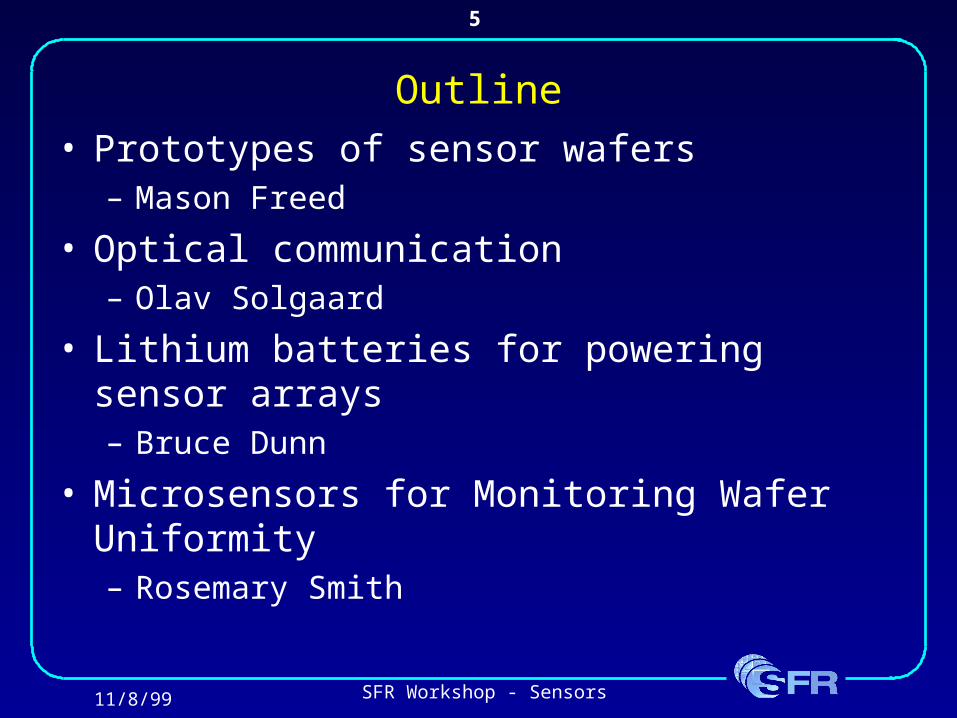
5
Outline
• Prototypes of sensor wafers– Mason Freed
• Optical communication – Olav Solgaard
• Lithium batteries for powering sensor arrays– Bruce Dunn
• Microsensors for Monitoring Wafer Uniformity– Rosemary Smith

11/8/99 SFR Workshop - Sensors
6
Prototypes of Sensor Wafers
Mason Freed, Darin Fisher, Michiel Kruger
Andy Gleckman, Scott Eitapence, Tim Duncan, Kevin Cho,
Costas Spanos, Kameshwar Poolla

11/8/99 SFR Workshop - Sensors
7
Division of Research• Power, communications,
and isolation– Use readily available sensors
and electronics
– Try different power, communication, and isolation options
• Integrated transducers – Use wired power and
communications
– Research novel sensor structures

11/8/99 SFR Workshop - Sensors
8
Component-Based Approach
• Technology set– Surface mount components only
– Minimal processing of host wafer (metal lines only)
– On-board microprocessor
– Off-the-shelf battery technology
• Features– Distributed array of sensors
– Real-time data acquisition
– Wireless power & data transfer

11/8/99 SFR Workshop - Sensors
9
Temperature Sensor• Useful for DUV resist bake monitoring • Objectives
– Monitor wafer temperature at 4 locations (within 0.5ºC)
– PalmPilot inter-operability
• Design– Off-the-shelf temperature sensor modules
– PIC microprocessor (with integrated 4 channel A/D)
– Infrared data transfer (IrDA compliant)
– Error detection (CRC-16)

11/8/99 SFR Workshop - Sensors
10
The Wafers
Ir-LED
P
Batteries
Sensor
Ir-LED
P
Batteries
Sensor
Silver paste mount on Al
Direct SMD, on Al+nickel

11/8/99 SFR Workshop - Sensors
11
PalmPilot Interface

11/8/99 SFR Workshop - Sensors
12
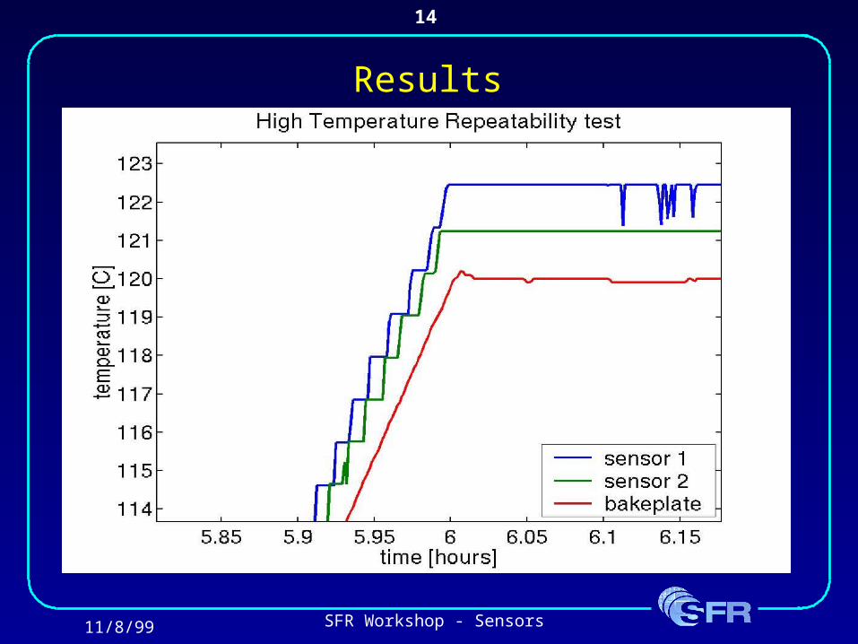
Long Term Reliability Testing• Computer-controlled bake plate used• Sensor output compared to actual temperature• Temperature cycling behavior evaluated
WaferIr-receiver
ProbesBake-plate
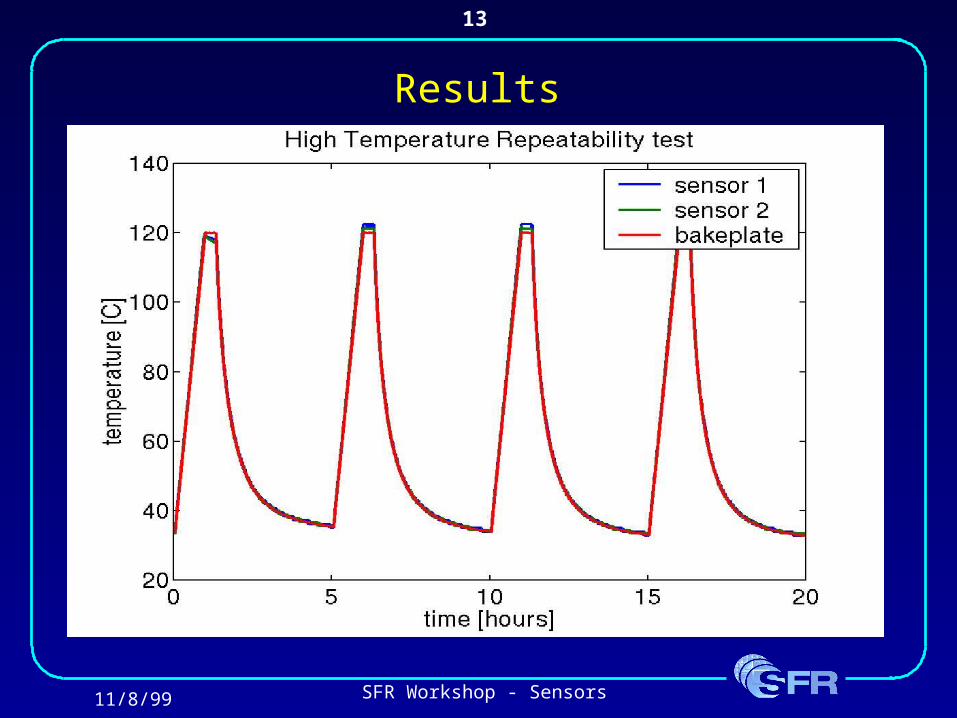
11/8/99 SFR Workshop - Sensors
13
Results
11/8/99 SFR Workshop - Sensors
14
Results

11/8/99 SFR Workshop - Sensors
15
Rapid Transient Temperature Readings

11/8/99 SFR Workshop - Sensors
16
Future Plans (Component-Based)
• Short Term– Work on passivation techniques
– Test in plasma-etch chamber
– Raise upper temp limit to 150°C
• Long Term– Move to flip-chip components (for reduced profile)
– Incorporate UCLA thin-battery technology
– Use other sensor types
– Implement closed loop control using data
– Measure thermal transient during DUV bake

11/8/99 SFR Workshop - Sensors
17
Integrated Transducer: Etch Rate + Temp
• Sensor to measure polysilicon etch rate• Based on van der Pauw probe electrical film-
thickness measurement:
VIt 2ln
I
I
Poly-Si
V
IV
ts 2ln

11/8/99 SFR Workshop - Sensors
18
Experimental Method• Use wired connections for power and communications
– Edge-board connector used to make connections to wafer• Initial testing in XeF2 etch chamber
– Isotropic, non-plasma gaseous etchant– No problem making connections to wafer– No electrical or physical isolation necessary

11/8/99 SFR Workshop - Sensors
19
Previous Design• No onboard electronics, only sensors• Simple, two-mask process• Features
– Three film-thickness sensors
– Polysilicon “guard ring” around sensors
– Clip-on wire connections
– Parallel connection of sensors

11/8/99 SFR Workshop - Sensors
20
Previous Design

11/8/99 SFR Workshop - Sensors
21
Results from old Design
• Eleven etch cycles performed, reflectometric thickness measurements made between each cycle
11/8/99 SFR Workshop - Sensors
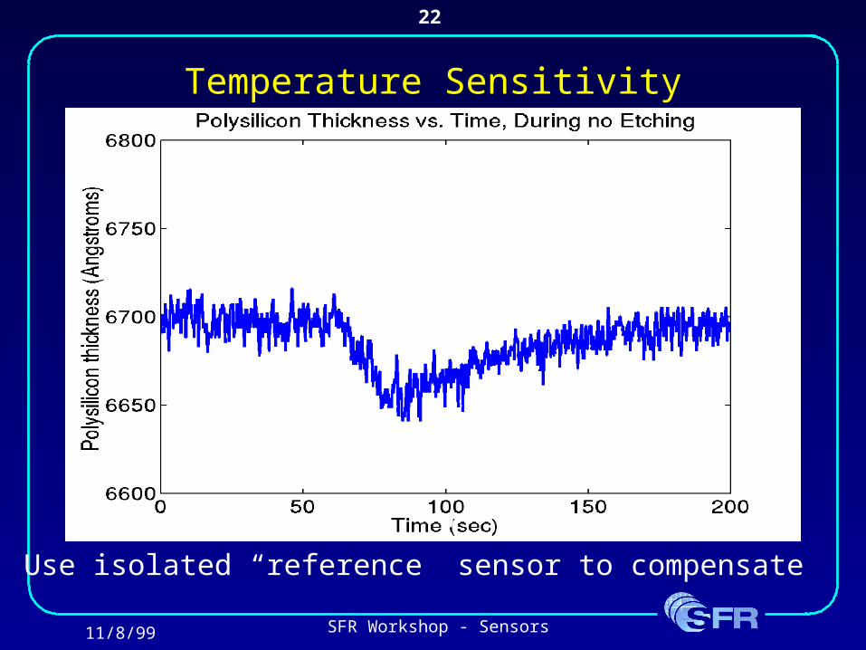
22
Temperature Sensitivity
Use isolated “reference” sensor to compensate

11/8/99 SFR Workshop - Sensors
23
Spatial Non-Uniformity Close-up
Make sensors smaller

11/8/99 SFR Workshop - Sensors
24
Rough Polysilicon Surface
For more heavily-etched samples, reflectometry fails Use profilometer instead

11/8/99 SFR Workshop - Sensors
25
Results from previous Integrated Etch-rate Sensor
• Repeatability: ~ 13Å• Accuracy: ~ 45.9 Å• Stability: < 5Å

11/8/99 SFR Workshop - Sensors
26
Latest Etch Rate Sensor Design• Surface mount analog multiplexers used
– Number of sensors increased to 16
• Sensors are smaller (200m on a side vs. 3000m)• Each sensor has a buried temperature reference
I
Buried
I
Exposed
VthVtemp

11/8/99 SFR Workshop - Sensors
27
Latest Design
11/8/99 SFR Workshop - Sensors
28
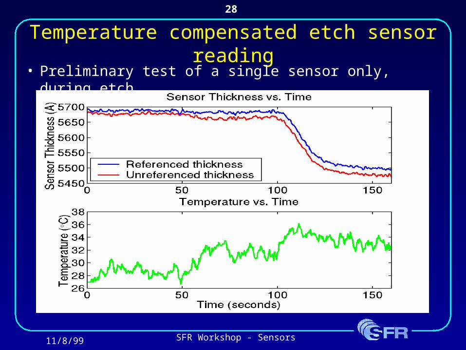
Temperature compensated etch sensor reading
• Preliminary test of a single sensor only, during etch

11/8/99 SFR Workshop - Sensors
29
Future Plans (Transducers)
• Test latest design
• Research isolation schemes to allow operation in plasma conditions
• Work on integrating power and communications modules onto sensor wafer, for wireless operation
• Develop sensors for other measurements in plasma
– Ion flux measurement in plasma etch
• Develop sensors other processes
– Wafer stress sensor for deposition processes

11/8/99 SFR Workshop - Sensors
30
Free-Space Communication for Autonomous Sensors using Grating Light
Modulators
David R. Pedersen, Michael H. Guddal
University of California, Davis
Olav Solgaard
Stanford University

11/8/99 SFR Workshop - Sensors
31
Outline• Summary of Year 1 Milestones
– Developed, modeled and characterized GLM
– Demonstrated free-space optical link using GCC modulator
• Improvements in GLM design– Reduce angle dependence and dispersion
– Increase damping
– No interference with plasma => “buried” GLM
• Year 2 Milestones– Integrate micromachined GLM with on-board power
– Buried GLM, through-the-wafer interconnects, wafer bonding

11/8/99 SFR Workshop - Sensors
32
GCC Communication Link
90 100 110 120-12
-10
-8
-6
-4
-2
0
2
4
6
actu
atio
n vo
ltage
(V
)
time (us)
4.4
4.8
5.2
5.6
6.0
6.4
6.8
7.2
detector signal
actuation force
actuation voltage
+/-5% steady-state
det
ecto
r vo
ltage
(V
)
-20
0
20
40
60

11/8/99 SFR Workshop - Sensors
33
High Contrast GLM
0 20 40 60 80 100 120 140 160 180 200-8
-6
-4
-2
0
2
4
6
actu
atio
n vo
ltage
(V
)
time (us)
1.8
2.0
2.2
2.4
2.6
2.8
3.0
3.2
3.4
+/-5% steady-state
+/-5% steady-state
detector
actuation
det
ecto
r vo
ltage
(V
)
Reflective State
Diffractive State
Reduced Angle dependence
Increased damping

11/8/99 SFR Workshop - Sensors
34
Full-wafer Grating Light Modulators
Period: 10Gap: 10mBeam Width: 10mSubstrate/Beam Spacing: 2umBeam Length: 200m to 600m
Beams: Doped low stress polysilicon Insulating Material: PSG
1. MASK 1 Pattern Backside Poly
2. MASK 2 Pattern GLM
3. Release and dry
4. Reoxidize to prevent shorting
5. Contact pads

11/8/99 SFR Workshop - Sensors
35
Layout
Back
Each line: 2mm open-circuit region etched to the substrate and aligned with the front
Backside contact to the substrate
Front

11/8/99 SFR Workshop - Sensors
36
Buried Grating Light Modulators - Technology Development
AR-coating
DRIE trenches for interconnects and corner-cube reflectors Oxidation-smoothed
TIR surface
GLM aperture

11/8/99 SFR Workshop - Sensors
37
Autonomous Sensor Wafer with Buried GLMs
Battery Electronics
Sensor array
Interconnects
Buried GLM

11/8/99 SFR Workshop - Sensors
38
Conclusion
• Met Year 1 Milestones:– Fabricated and tested micro-machined GLMs
– Demonstrated free-space communication
• Full-wafer fabrication process • Year 2 Milestones
– Integrate micromachined GLMs with on-board power, sensors, and electronics sources
• Technology development– Buried GLMs
– Through-the-wafer interconnects
– Wafer bonding

11/8/99 SFR Workshop - Sensors
39
Lithium Batteries for Powering Sensor Arrays
SFR Workshop
November 8, 1999
Bruce Dunn
UCLA
Student contributors: Nelson Chong, Brianna Fehlberg, Jimmy Lim, Jeff Sakamoto

11/8/99 SFR Workshop - Sensors
40
Progress Since May
• Battery encapsulation using two-layer system
• Battery operation under aggressive conditions– Vacuum
– Temperatures up to 85°C
• Battery encapsulated in wafer
11/8/99 SFR Workshop - Sensors
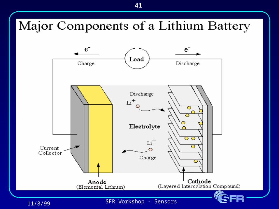
41

11/8/99 SFR Workshop - Sensors
42
2 Component Epoxy Mechanism
+
SN2 Reaction
Hardener(Amines)
Epoxy Resin RapidProtonTransfer
Possible Reactions with Lithium
Hydroxyl groups in Thermoset Epoxy
Amines from excess Hardener
Further EpoxyPolymerization(Cross-linking)
ThermosetEpoxy

11/8/99 SFR Workshop - Sensors
43
0
10
20
30
40
50
60
0 200 400 600 800 1000 1200
Uncoated
Time (Hour)
Impe
danc
e (
Ohm
s)
TMSA Coated
TMSA Protection of Lithium
Si
CH3
H3C
CH3
C CH
Trimethylsilylacetylene (TMSA)
Working Electrode
Reference ElectrodeCounter Electrode(Anode)
Lithium Lithium
Liquid Electrolyte1 M LiClO4 in Propylene Carbonate
TMSA coated Li
TMSA coating prevents adverse lithium reactions

11/8/99 SFR Workshop - Sensors
44
Side by Side Battery Profiles
Top Profile of 7 voltbattery on OxidizedSilicon Waferencapsulated by Epoxy
Side Profile
Stainless Steel
Vanadium Pentoxide (V2O5)
Lithium Foil
PAN based Electrolyte
Celgard ® 3401
Trimethylsilylacetylene (TMSA)
Thermoset Epoxy
Oxidized Silicon Wafer

11/8/99 SFR Workshop - Sensors
45
Side by Side Battery Fabrication
V2O 5 Sprayed Electrodeson Stainless Steel FoilVacuum Heated 1 Hour
Transferredinto ArgonGlove Box
Electrolyte Applicationover Cellguard® sheets
Electrode leads placedover electrolyte
Battery placed on OxidizedSilicon Wafer and coatedwith TMSA
Battery encapsulatedby Epoxy
Celgard® 3401placed on both sidesover electrolyte
Electrolyte Applicationby Spatula on both V2O 5and Lithium on baseplate electrode
PAN based electrolyteheated in Silicon Oilbath at 125oC
Lithium Foilpressed onelectrodes
11/8/99 SFR Workshop - Sensors
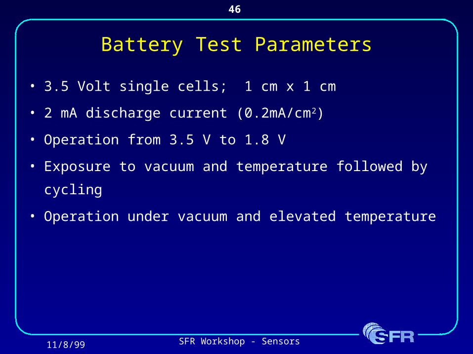
46
Battery Test Parameters
• 3.5 Volt single cells; 1 cm x 1 cm
• 2 mA discharge current (0.2mA/cm2)
• Operation from 3.5 V to 1.8 V
• Exposure to vacuum and temperature followed by cycling
• Operation under vacuum and elevated temperature

11/8/99 SFR Workshop - Sensors
47
Comparison of Encapsulated and Packaged Battery
0
0.05
0.1
0.15
0.2
0.25
0.3
0 1 2 3 4 5 6
Cycle
Ca
pa
cit
y (
mA
h/c
m2)
Battery in Epoxy
Battery in Bag
0
0.5
1
1.5
2
2.5
3
3.5
4
4.5
0 1000 2000 3000 4000 5000 6000 7000 8000 9000
Time (seconds)
Vo
lta
ge
Encapsulated battery comparable to packaged; 3 cm x 3 cm cell toprovide > 2 mAh capacity
Discharge at 1 mA/cm2
5 cycles
11/8/99 SFR Workshop - Sensors
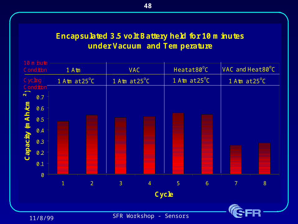
48
Encapsulated 3.5 volt Battery held for 10 m inutes under Vacuum and Temperature
0
0.1
0.2
0.3
0.4
0.5
0.6
0.7
0.8
0.9
1
1 2 3 4 5 6 7 8
Cycle
Cap
acit
y (m
Ah
/cm
2)
10 minute Condition
Cycling Condition
VAC
1 Atm at 25oC 1 Atm at 25oC 1 Atm at 25oC 1 Atm at 25oC
1 Atm Heat at 80oC VAC and Heat 80oC

11/8/99 SFR Workshop - Sensors
49
Operation of 3.5 Volt Battery at Temperature and Vacuum
0
0.05
0.1
0.15
0.2
0.25
0.3
0.35
0.4
0.45
0.5
1 2 3 4 5 6 7 8 9 10 11 12
Cycle
Ca
pa
cit
y (m
Ah
/cm
2)
Atm
Temp
VACVAC VAC11 1
25oC 25oC 25oC 80oC 80oC 80oC

11/8/99 SFR Workshop - Sensors
50
Present Direction: Wafer With Encapsulated Battery Connection
to sensor grid
Ni Wire
Epoxy
Al Wire
SiO2
Ni Current Collector
Lithium Anode
Polymer Electrolyte
Vanadia Cathode
Al Current Collector
trimethylsilylacetylene
Multi-layer encapsulation scheme
11/8/99 SFR Workshop - Sensors
51
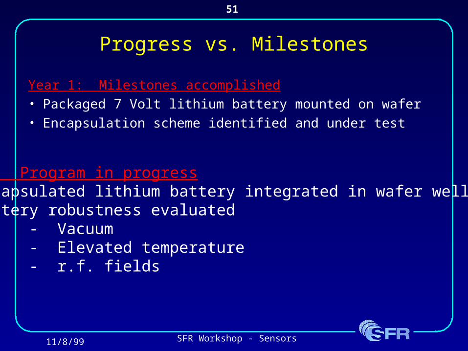
Progress vs. Milestones
Year 1: Milestones accomplished
• Packaged 7 Volt lithium battery mounted on wafer
• Encapsulation scheme identified and under test
Year 2: Program in progress • Encapsulated lithium battery integrated in wafer well• Battery robustness evaluated
- Vacuum- Elevated temperature- r.f. fields

11/8/99 SFR Workshop - Sensors
52
Plans for 2000 - 2002
• Develop higher temperature capability (150°C)– Utilize higher temperature component materials
• Construct battery directly on wafer– Integrate materials processing into battery fabrication

11/8/99 SFR Workshop - Sensors
53
Microsensors for Monitoring Wafer Uniformity of Plasma Processes
Ribi Leung, Dwight Howard, Scott D. Collins,
and Rosemary L. Smith
MicroInstruments and Systems LaboratoryMicroInstruments and Systems Laboratory
UCDavis

11/8/99 SFR Workshop - Sensors
54
Abstract• The goal of this project is to realize specific
microsensors for in situ plasma process monitoring. • Thin, multilayer, metal film resistors are being
evaluated as surface peak temperature recording devices.
– Au/Cr resistors, which are effective for 150 <T < 250 C, have been fabricated and tested in an ECR plasma tool.
– Au/Al and Au/Cr/Al resistors are being evaluated for detection of T≤150C.
– An RIE undercut sensor has been designed and is in the testing phase.
• Temperature and undercut sensors will be integrated for combined measurements later this year.

11/8/99 SFR Workshop - Sensors
55
Relevant Milestones• June 1999
– Evaluate wafer surface temperature variation during RIE processing using Au/Cr resistor array.
• June 2000– Optimize materials for temperature sensitivity and range.
– Test undercut sensors in RIE.
– Test integrated Temperature and undercut sensors in RIE.
– Determine wafer variation in specific RIE tools.

11/8/99 SFR Workshop - Sensors
56
Interdiffusion of Cr / Au
TIME FUNCTIONS (3, 6, and 10 min.)
0.91
1.11.21.31.41.51.61.71.8
150 170 190 210 230 250
Temperature (C)

11/8/99 SFR Workshop - Sensors
57
Thin Film Resistor Pattern
500 µm
Ri = 670 ž

11/8/99 SFR Workshop - Sensors
58
RIE Experiments
• Plasmaquest, Electron Cyclotron Resonance (ECR) RIE
• Sample: 4” Wafer, Cr/Au on SiO2, coated with photoresist
• Power= 1200 W, 2.45 GHz, Ar@ 2mTorr, time = 5 minutes
-- No substrate cooling --
150 Watt Bias --> Surface Temperature > 200C
0 Watt Bias --> Surface Temp ≤ 100 C (∆R≈0)
150 Watt Bias, only 3 minutes --> ∆R≈0
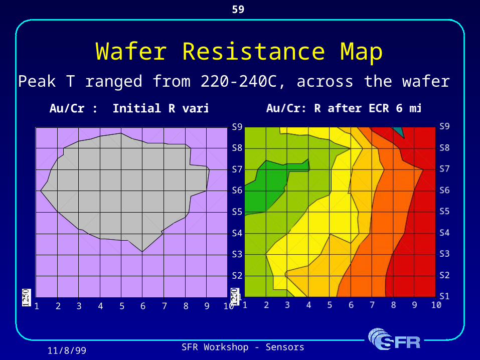
11/8/99 SFR Workshop - Sensors
59
1 2 3 4 5 6 7 8 9 10
S1
S2
S3
S4
S5
S6
S7
S8
S9
Au/Cr : Initial R variation
Wafer Resistance MapPeak T ranged from 220-240C, across the wafer

11/8/99 SFR Workshop - Sensors
60
Interdiffusion of Au / Al
Au/Cr
2.00
2.50
3.00
3.50
4.00
4.50
5.00
5.50
6.00
25 50 70 90 110 130 150 170 190 210 230 250
DEGREES CENTIGRADE
Au/Al
OHMS
color change
11/8/99 SFR Workshop - Sensors
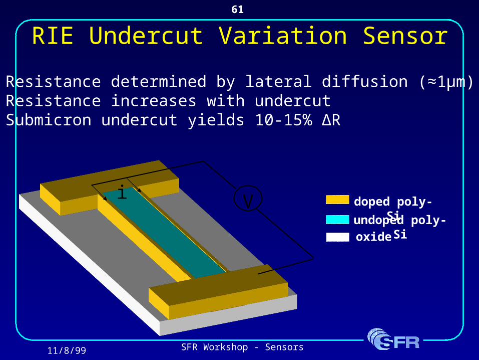
61
RIE Undercut Variation Sensor
I
• Resistance determined by lateral diffusion (≈1µm)• Resistance increases with undercut• Submicron undercut yields 10-15% ∆R
i V
oxide
doped poly-Si
undoped poly-Si
11/8/99 SFR Workshop - Sensors
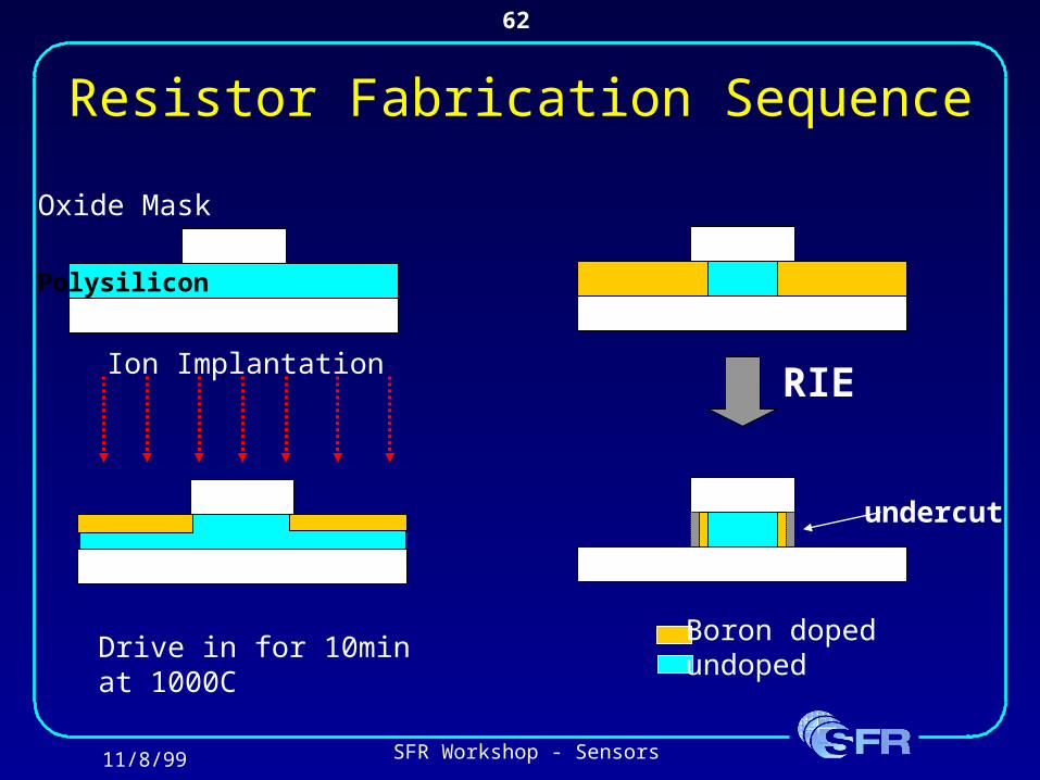
62
Resistor Fabrication Sequence
Oxide Mask
Polysilicon
Ion Implantation
Boron dopedundoped
RIE
undercut
Drive in for 10min at 1000C

11/8/99 SFR Workshop - Sensors
63
Lateral Diffusion after Drive-in
11/8/99 SFR Workshop - Sensors
64
Continuing Work
• RIE undercut variation determination/ demonstration of sensor
• Evaluate Au/Al structures for room T stability. Stabilize, if necessary, with interposed layer of Cr.
• Integration of temperature mapping with RIE etch -rate and degree of undercut

11/8/99 SFR Workshop - Sensors
65
Future Directions?A MEMS Device for T Mapping versus Time
Plasma Etch/Deposition Mask
Thermal Expansion Joint
T0 Position
T1 >T0 Position
Window
Varying Etch Depths
Thermal microactuator positions shadow mask over etch/deposition window, creating steps in film height. Location of step edge corresponds to Temperature, height indicates time.
11/8/99 SFR Workshop - Sensors
66
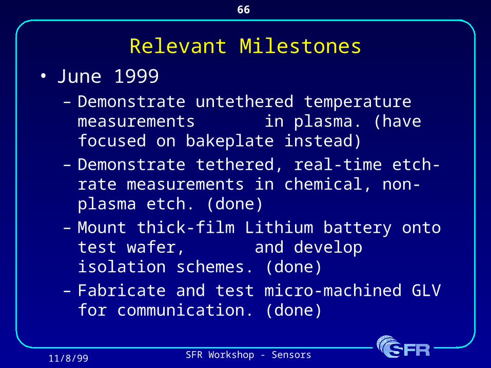
Relevant Milestones
• June 1999– Demonstrate untethered temperature measurements
in plasma. (have focused on bakeplate instead)
– Demonstrate tethered, real-time etch-rate measurements in chemical, non-plasma etch. (done)
– Mount thick-film Lithium battery onto test wafer, and develop isolation schemes. (done)
– Fabricate and test micro-machined GLV for communication. (done)
11/8/99 SFR Workshop - Sensors
67
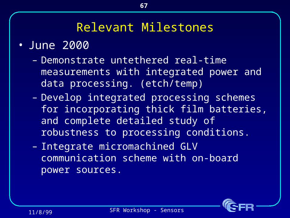
Relevant Milestones
• June 2000– Demonstrate untethered real-time measurements with
integrated power and data processing. (etch/temp)
– Develop integrated processing schemes for incorporating thick film batteries, and complete detailed study of robustness to processing conditions.
– Integrate micromachined GLV communication scheme with on-board power sources.

11/8/99 SFR Workshop - Sensors
68
Future Plans
• New sensors– Ion flux
– Stress profile
– DUV latent image
• Modular platform development– Host wafer, generic sensor module
– Manufacturing issues

11/8/99 SFR Workshop - Sensors
69
Future Plans (Continued)
• Applications: these sensors can be very useful– Close a control loop to demonstrate non-uniformity
reduction
– Demonstrate reduced need for test wafers in process design / qualification
– Use sensor data to calibrate DUV resist models
– Investigate extensions to large-area wafer processing
• Successful completion of these goals will require extensive participation with industrial sponsors
Related Documents