10 nm CMOS: 10 nm CMOS: The Prospects for III-Vs J. A. del Alamo, Dae-Hyun Kim 1 , Donghyun Jin, and Taewoo Kim Microsystems Technology Laboratories, MIT 1 Presently with Teledyne Scientific 2010 European Materials Research Society Spring Meeting June 7-10 2010 Sponsors: Intel, FCRP-MSD Acknowledgements: June 7-10, 2010 1 Acknowledgements: Niamh Waldron, Ling Xia, Dimitri Antoniadis, Robert Chau MTL, NSL, SEBL

Welcome message from author
This document is posted to help you gain knowledge. Please leave a comment to let me know what you think about it! Share it to your friends and learn new things together.
Transcript

10 nm CMOS:10 nm CMOS: The Prospects for III-Vs
J. A. del Alamo, Dae-Hyun Kim1, Donghyun Jin, and Taewoo Kim
Microsystems Technology Laboratories, MIT1Presently with Teledyne Scientific
2010 European Materials Research Society Spring MeetingJune 7-10 2010
Sponsors: Intel, FCRP-MSD
Acknowledgements:
June 7-10, 2010
1
Acknowledgements:
Niamh Waldron, Ling Xia, Dimitri Antoniadis, Robert Chau
MTL, NSL, SEBL
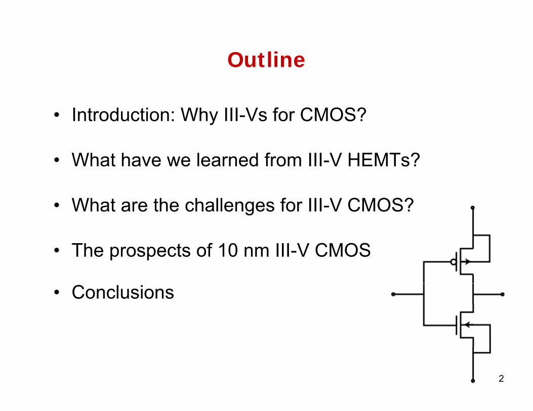
Outline
• Introduction: Why III-Vs for CMOS?
• What have we learned from III-V HEMTs?
• What are the challenges for III-V CMOS?
• The prospects of 10 nm III-V CMOS
• Conclusions
22

Why III-Vs for CMOS?
• Si CMOS has entered era of “power-constrained scaling”:– CPU power density saturated at ~100 W/cm2
– CPU clock speed saturated at ~ 4 GHz
P N R 2010 http://www chem utoronto ca/ nlipkowi/pictures/cloPop, Nano Res 2010 http://www.chem.utoronto.ca/~nlipkowi/pictures/clockspeeds.gif
3
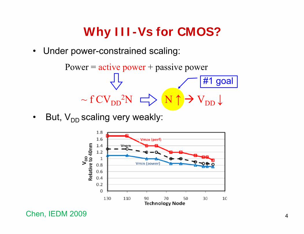
Why III-Vs for CMOS?• Under power-constrained scaling:
Power = active power + passive power
~ f CVDD2N N ↑ VDD↓
#1 goal
• But, VDD scaling very weakly:
f CVDD N N ↑ VDD ↓V D
D
4V
4Chen, IEDM 2009

Why III-Vs for CMOS?
• Need scaling approach that allows VDD reduction
• Goal of scaling: – reduce footprint – extract maximum ION for given IOFF
III V• III-Vs:– Much higher injection velocity than Si ION ↑ON
– Very tight carrier confinement possible S↓
55

III-V CMOS: What are the challenges?
“To kno here o are going o first ha e to“To know where you are going, you first have to know where you are.”
We are starting from:g
III-V High Electron Mobility Transistors
66
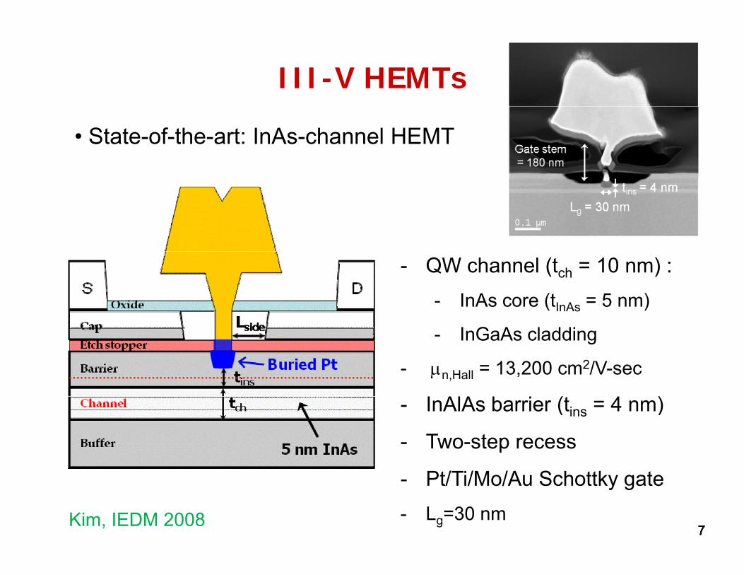
III-V HEMTs
• State-of-the-art: InAs-channel HEMT
- QW channel (tch = 10 nm) :- InAs core (tInAs = 5 nm)
- InGaAs cladding
- n,Hall = 13,200 cm2/V-sec
I AlA b i ( 4 )- InAlAs barrier (tins = 4 nm)
- Two-step recess
7777
- Pt/Ti/Mo/Au Schottky gate- Lg=30 nm Kim, IEDM 2008
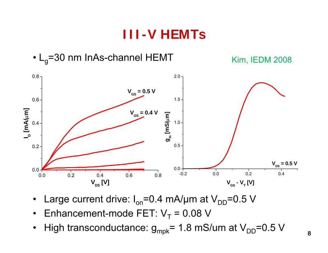
III-V HEMTs
0.8
• Lg=30 nm InAs-channel HEMT Kim, IEDM 2008
2.0
0.6
V 0 4 Vm]
VGS = 0.5 V1.5
0.4
VGS = 0.4 V
I D [m
A/
m
1.0
g m [m
S/m
]0 0 0 2 0 4 0 6 0 8
0.0
0.2
-0 2 0 0 0 2 0 40.0
0.5
VDS = 0.5 V
0.0 0.2 0.4 0.6 0.8VDS [V]
• Large current drive: Ion=0.4 mA/µm at VDD=0.5 V
0.2 0.0 0.2 0.4
VGS - VT [V]
888
• Enhancement-mode FET: VT = 0.08 V• High transconductance: gmpk= 1.8 mS/um at VDD=0.5 V
8
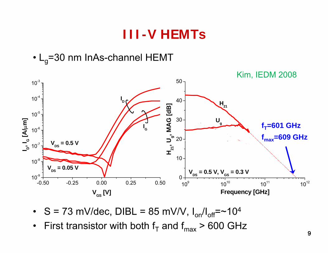
III-V HEMTs
• Lg=30 nm InAs-channel HEMT
Kim, IEDM 2008
10-4
10-3
ID 40
50
dB] H21
10-6
10-5
IG
V = 0 5 VI G [A
/m
]
20
30
Ug,
MA
G [d
Ug
MAG
fT=601 GHzfmax=609 GHz
9
10-8
10-7 VDS = 0.5 V
I D, I
VDS = 0.05 V10
H21
, MAG
VDS = 0.5 V, VGS = 0.3 V
-0.50 -0.25 0.00 0.25 0.5010-9
VGS [V]109 1010 1011 1012
0
Frequency [GHz]
DS , GS
999
• S = 73 mV/dec, DIBL = 85 mV/V, Ion/Ioff=~104
• First transistor with both fT and fmax > 600 GHz9
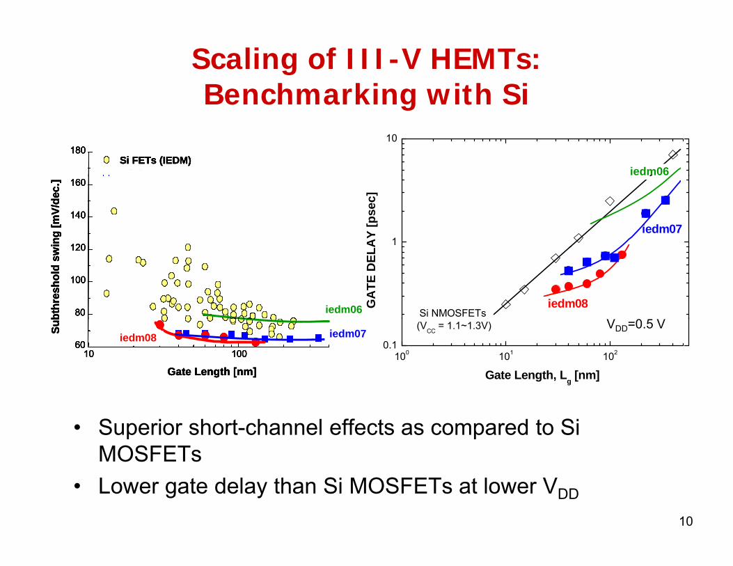
Scaling of III-V HEMTs: Benchmarking with Si
180Si FETs (IEDM)Triple recess: IEDM 07
180Si FETs (IEDM)Triple recess: IEDM 07
180Si FETs (IEDM)*
180Si FETs (IEDM)*
e c a g t S10
iedm06
120
140
160
win
g [m
V/de
c.] Triple recess: IEDM 07
Pt sinking
120
140
160
win
g [m
V/de
c.] Triple recess: IEDM 07
Pt sinking
120
140
160
win
g [m
V/de
c.] Pt sinking: IEDM 08
120
140
160
win
g [m
V/de
c.] Pt sinking: IEDM 08
1iedm07
AY
[pse
c]
80
100
120
bthr
esho
ldsw
80
100
120
bthr
esho
ldsw
80
100
120
bthr
esho
ldsw
80
100
120
bthr
esho
ldsw
iedm06
InAs HEMTs(VCC = 0.5V)
GA
TE D
EL
Si NMOSFETsiedm08
10 10060
Sub
Gate Length [nm]10 100
60
Sub
Gate Length [nm]10 100
60
Sub
Gate Length [nm]10 100
60
Sub
Gate Length [nm]
iedm07iedm08
100 101 1020.1
Gate Length, Lg [nm]
(VCC = 1.1~1.3V) VDD=0.5 V
• Superior short-channel effects as compared to Si MOSFETsOS s
• Lower gate delay than Si MOSFETs at lower VDD
10

Scaling of III-V HEMTs: Benchmarking with Si
• ION @ IOFF=100 nA/µm, VDD=0.5 V: FOM that integrates short-channel effects and drive current
e c a g t S
(scaled to VDD=0.5 V)
III-V HEMTs: higher ION for same IOFF than Si11

What can we learn from III-V HEMTs?
1. Very high electron injection velocity at the virtual source
Evinj
Kim, IEDM 2009
EC
njL0 x
vinj ≡ electron injection
v inj
j
velocity at virtual source
(I G A ) i ith I A f ti i h l• vinj(InGaAs) increases with InAs fraction in channel• vinj(InGaAs) > 2vinj(Si) at less than half VDD
12

What can we learn from III-V HEMTs?2. Quantum-well channel key to outstanding short-channel
effectsKim IPRM 2010Kim, IPRM 2010
D ti i t i l t t ti i t it i thi• Dramatic improvement in electrostatic integrity in thin channel devices
13
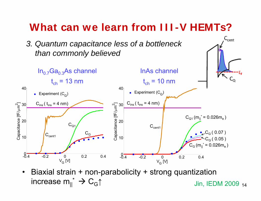
What can we learn from III-V HEMTs?3. Quantum capacitance less of a bottleneck
than commonly believed
In0.7Ga0.3As channel tch = 13 nm
InAs channeltch = 10 nm
40 40
30
40
F/ m
2 ]
Experiment (CG)
Cins ( tins = 4 nm) 30
40
F/ m
2 ]
Experiment (CG)
Cins ( tins = 4 nm)
10
20
Cap
acita
nce
[fF
CQ1
CGCcent1 10
20C
apac
itanc
e [fF
Ccent1
CQ1 (m||* = 0.026me )
CG ( 0.07 ) C ( 0 05 )
-0.4 -0.2 0 0.2 0.40
10
VG [V]
C
-0.4 -0.2 0 0.2 0.40
10
VG [V]
C
CG (m||* = 0.026me ) CG ( 0.05 )
G
• Biaxial strain + non-parabolicity + strong quantization increase m||
* CG↑ Jin, IEDM 2009 14
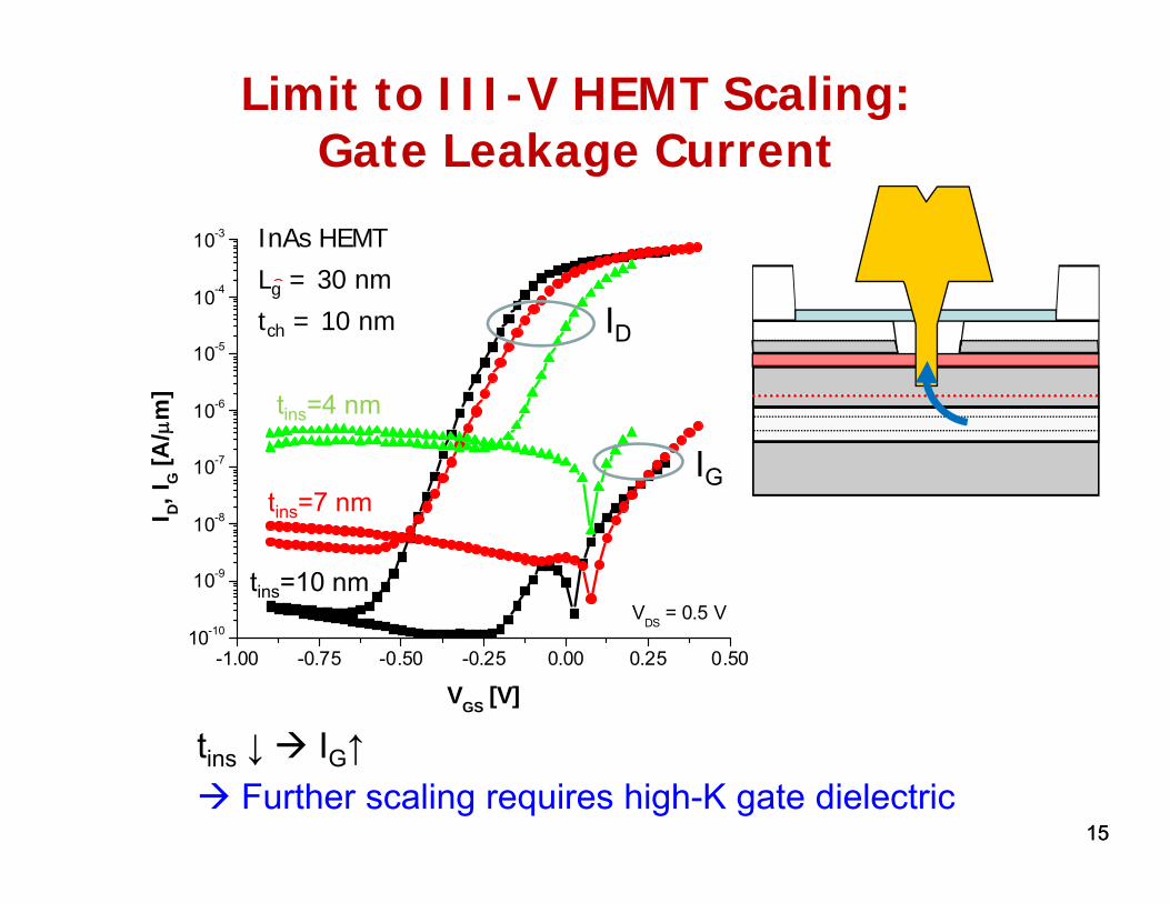
Limit to III-V HEMT Scaling: Gate Leakage Current
10-3
tins
= 10 nmt = 7 nm
Gate ea age Cu e t
InAs HEMTL = 30 nm
10-5
10-4
]
tins = 7 nm t
ins = 4 nm ID
Lg = 30 nmtch = 10 nm
4
10-7
10-6
D, I G
[A/
m]
IG
tins=4 nm
tins=7 nm
10-9
10-8
VDS
= 0.5 V
I D tins 7 nm
tins=10 nm
-1.00 -0.75 -0.50 -0.25 0.00 0.25 0.5010-10
DS
VGS [V]
t ↓ I ↑
15
tins ↓ IG↑ Further scaling requires high-K gate dielectric
15
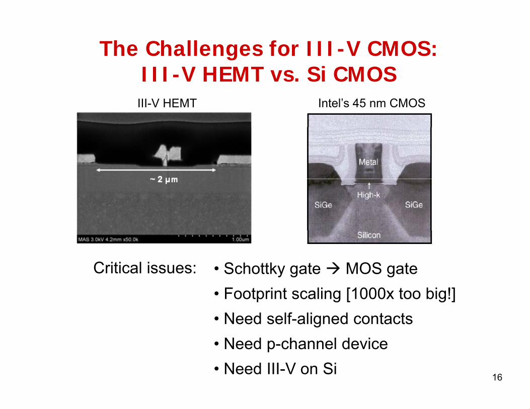
The Challenges for III-V CMOS: III-V HEMT vs Si CMOSIII-V HEMT vs. Si CMOS
Intel’s 45 nm CMOSIII-V HEMT
• Schottky gate MOS gate Critical issues:• Footprint scaling [1000x too big!] • Need self-aligned contacts
16
• Need p-channel device• Need III-V on Si

The High-K/III-V System by ALD
• Ex-situ ALD produces high-quality interface on InGaAs:– Surface inversion demonstrated
11 2 1Al2O3/In0.52Ga0.47As
– Dit in mid ~1011 cm-2.eV-1 demonstrated
Al2O3/In0.52Ga0.47As
f=100 Hz-1 MHz
2 00E 011
2.40E-011 In0.65Ga0.35As MOS-CapCgb on D=75um
Al2O3/In0.65Ga0.35As
1.20E-011
1.60E-011
2.00E-011
fT~55.56KHz
Cap
acita
nce
(F)
Lin, SISC 2008
1717
Ye, 2010-6 -4 -2 0 2 4
4.00E-012
8.00E-012
Bias (V)
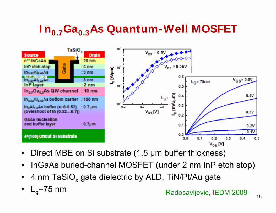
In0.7Ga0.3As Quantum-Well MOSFET
• Direct MBE on Si substrate (1.5 µm buffer thickness)• InGaAs buried-channel MOSFET (under 2 nm InP etch stop)
S O / /• 4 nm TaSiOx gate dielectric by ALD, TiN/Pt/Au gate• Lg=75 nm
18Radosavljevic, IEDM 2009

In0.7Ga0.3As Quantum-Well MOSFET
2009 Intel InGaAs MOSFET(scaled to
VDD=0.5 V)
19

What can we expect from10 nm III V NMOS at 0 5 V?~10 nm III-V NMOS at 0.5 V?
With thin InAs channel:
Assume RS as in Si (~80 Ω.µm):
K i tThree greatest worries!
S
ID=1.5 mA/µm
Key requirements:• High-K/III-V interface, thin channel do not degrade vinj
• Obtaining R =80 Ω µm at required footprint
worries!
• Obtaining Rs=80 Ω.µm at required footprint• Acceptable short-channel effects
20

Conclusions• III-Vs attractive for CMOS: key for low VDD operation
– Electron injection velocity in InAs > 2X that of Si at 1/2X VDD
Quantum well channel yields outstanding short channel effects– Quantum well channel yields outstanding short-channel effects– Quantum capacitance less of a limitation than previously believed
• Impressive recent progress on III-V CMOS – Ex-situ ALD and MOCVD on InGaAs yield interfaces with unpinned
Fermi level and low defect densityFermi level and low defect density– Sub-100 nm InGaAs MOSFETs with ION > than Si at 0.5 V
demonstrated
• Lots of work ahead:– Demonstrate 10 nm III-V MOSFET that is better than Si
21
– P-channel MOSFET– Manufacturability, reliability
Related Documents