1 Optical Diffraction Theory and Its Applications on Photonic Device Design

1 Optical Diffraction Theory and Its Applications on Photonic Device Design.
Dec 28, 2015
Welcome message from author
This document is posted to help you gain knowledge. Please leave a comment to let me know what you think about it! Share it to your friends and learn new things together.
Transcript

1
Optical Diffraction Theory and Its Applications on
Photonic Device Design

2
Diffraction
SourceFree Space
Plane Wave
Waveguideor resonator
Wave guidance for power or signal transmission
Wave manipulation for other purposes
Diffraction as a natural evolving process towards the plane wave
Direct applications: broadcasting, satellite comm., radar, etc.

3
Models for Diffraction and Scattering
Diffraction Scattering
>>D
D
D
Characteristics of the diffracted/scattered EM fields and the simulation models differ depending on the relative magnitude of the wavelength and
feature size of the object.
<<D
Quasi-Static Geometric Optics
≈D
Full Wave
Single Pole Multi Poles
Ray

4
E
H = j E J
E j H M
Generalized Maxwell’s equations in homogeneous medium
mH
2( ) ( )E E E j H M
2( ) ( )E j j E J M
2 2 1E E j J M
Generalized wave equations in homogeneous medium
2 2 1mH H j M J
Generalized Wave Equations

5
Kirchhoff’s Diffraction Formula
MJEE μjωρε
1μεω22 JMHH εjωρ
μ
1μεω m
22
rrrr,rr, δεgμωg 22 rr
rrrr,
π4
jkexpg
Scalar Green’s Function
sd
n
g
ngvdgg 22 EE
EEn
E,H
EnM s ˆHnJ s ˆ
Region 1
V
SJ,M
n̂
n
vdμεgωgμεωgvdgg 222222 EEEEE
rErrEE vdδvdgμεω22
vdμjωρε
1gvdμεωg 22 MJEE
sd
n
g
ng vdgμjω
ε
ρE
EMJE
sdn
g
ng vdgjω
μ
ρm HH
JMH ε
Note: The integral is for closed surface only!

6
Diffraction Formulas for Open Surfaces
E,HEnM s ˆ
HnJ s ˆ
S dl
ds'C
r
r'
n̂
O
Line integrals enclosing the surface must be added to amend Kirchhoff’s formula:
ρ gjωμ g dv g ds
ε n n
1g d g d
jωC C
EE J M E
E l H l
mρ gjω g dv g ds
μ n n
1g d g d
jωC C
ε
HH M J H
H l E l

7
P1(x1,y1,z1)
P2(x2,y2,z2)
Q(ξ,η,0)
O
x
y
z
R1
r' R2
r2
r1
Diffraction by Aperture
rrR 11 rrR 22
21
2111 rrr2rR rr 2
22222 rrr2rR rr
11 1
1
exp jkRE A
R
2
2
exp jkRg
4 πR
Spherical wave at Q from P1 Spherical wave at P2 from Q

8
sd
n
gE
n
EgE 1
1
11 1
1 1 21 2
ˆ ˆˆ ˆE jAgE g E ds exp jk R R ds
n n 2λ R R
2n R n R
Diffracted Field:
11 R
ˆ
R 111 1 1
1 1
exp jkRE 1ˆˆ ˆE jk An R R
n n R
22
2 2
exp jkRg 1ˆˆ ˆg jkn R 4 πR
n n R
Ignore terms of 1/R³ if R>>
Diffracted Field
22 R
ˆ
R
R1
R2n̂
o
Q
P1
P2r1
r2
r'
2
1

9
1
11 2
1 2
ˆ ˆˆ ˆj A 1E exp jkR exp jkR ds
2 λ R R
2n R n R
Spherical wave at the aperture Q from P1
Spherical wave at the point P2 from Q
Inclination factor corrected by Kirchhoff
Physical Interpretation of Kirchhoff’s Integral
Original Huygens Principle
The diffracted field is a superposition of spherical waves emanating from the wavefront of another spherical wave originating from the point source.
R1
R2n̂
o
Q
P1
P2r1
r2
r'
2
1
For backward wave:
0ˆˆˆˆ 1 RnRn 2
For forward wave:
cosθ2ˆˆˆˆ 1 RnRn 2

10
Free-space field at P2 from P1
1 20 1
1 2
exp jk r rE A
r r
Diffraction Coefficient
2 1 1 2 1 20
E jˆ ˆ ˆ ˆD exp jk R R r r ds
E 2 λF n r n r
21 r
1
r
1
F
1
11 1
1 1 21 2
ˆ ˆˆ ˆE jAgE g E ds exp jk R R ds
n n 2λ R R
2n R n R
11 2
1 2
ˆ ˆ ˆ ˆjAE exp jk R R ds
2 λ r r
2 1n r n r
Diffraction Coefficient
F: Focus length

11
Different Approximations for Kirchhoff’s Integral
2i
iii
2ii
iii
ˆr2
1ˆr
rr
ˆ21rR
rrrrrr
rrrr
R1
R2n̂
o
Q
P1
P2
r1
r2
r'
Wavefront curvature correction
Plane wavefront correction
Spherical wave centered at Pi
i=1,2
Fresnel Diffraction
Fraunhofer Diffraction
Geometrical Optics
2iii i
i i i
exp jkrexp jkR kˆ ˆexp jk exp j
R r 2 r
r r r r r r

12
Expression of Diffraction Coefficient
2
22
1
21
212121 r2
ˆ
r2
ˆˆˆrrRR
rrrrrrrrrrr
2 1 1 2 1 2
jˆ ˆ ˆ ˆD exp jk R R r r ds
2λF
n r n r
2 1ˆ ˆ ˆ ˆ
D j exp jkf η,ξ ds2λF
n r n r
2222
1111
zˆyˆxˆ
zˆyˆxˆ
yyxr
zyxr
ξˆηˆ yxr
1
111 r
ξyηxˆ
rr
2
222
1
21122
212121 r2
ξnηm
r2
ξnηmξη
r
1
r
1
2
1ξnnηmmξη,f
2
222 r
ξyηxˆ
rr
ξη,frrRR 2121
1
11 r
xm
1
11 r
yn
2
22 r
yn
2
22 r
xm

13
Fresnel Diffraction
R1
R2
o
QP1
P2
r1
r2
r'
x2
z2
z1
x1 n̂
2
1
21 ˆˆˆ rzr
1122 ˆˆcosθcosθˆˆ rnrn 2211 sinθmsinθm
0yy 21
22
22 ξθcosηF2
1ξη,f
21 r
1
r
1
F
1
2 2
1 1
2 2 22 2jcosθ η ξ cos θ
D exp jk d dλF 2F
η

14
2 1ˆ ˆ ˆ ˆ
D j exp jkf η,ξ ds2 λF
n r n r
ξnnηmmξη,f 2121
2
2
1
1x r
x
r
xkk
2
2
1
1y r
y
r
ykk
2
222
1
21122
212121 r2
ξnηm
r2
ξnηmξη
r
1
r
1
2
1ξnnηmmξη,f
Fraunhofer Diffraction
Neglect the higher order terms in η and ξ
2 1x y
ˆ ˆ ˆ ˆD j exp j k η k ξ d d
2λFη ξ
n r n r
15
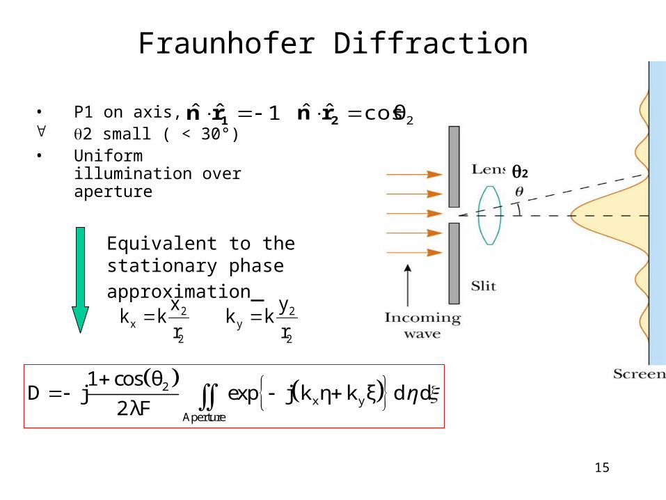
Fraunhofer Diffraction
• P1 on axis, 2 small ( < 30°)• Uniform illumination
over aperture
1ˆˆ 1rn 2cosθˆˆ 2rn
2
2x y
Aperture
1 cos θD j exp j k η k ξ d d
2λFη
2
2x r
xkk
2
2y r
ykk
Equivalent to the stationary
phase approximation

16
Fresnel and Fraunhofer Diffraction
• In Fraunhofer diffraction, both incident and diffracted waves may be considered to be plane (i.e. both S and P are a large distance away)
• If either S or P are close enough that wavefront curvature is not negligible, then we have Fresnel diffraction
P
S

17
Fraunhofer Diffraction
For non-uniform illumination at the aperture, and by restoring the free
space field factor, we find: 2 2 2
020
0 0 0 02 2 2 2 2 20 0
( , , ) ( , )j x y z zje
E x y z z DE Ax y z x y z
0 022 2 2 2
2 0
1 cos( )cos( )
2
z z
r x y z
2 2 2
2 0F r x y z where
0 0
0 02 2 2 2 2 20 0
2 ( )0 0
,( , ) ( , , 0) |j x y
x y
x y z x y z
A E x y z e dxdy
The coordinates in the new system are all normalized by the wavelength, i.e.,
( , , ) ( , , ) /x y z x y z

18
Plane Wave Propagation in Free Space
In homogeneous medium, the plane wave solution to Maxwell’s equations
can be expressed as: 0
2( )( ) ( ) 2 ( )
0 0 0 0x y z
j x y zj k x k y k z jk x y z j x y zE e E e E e E e
2 21 By assuming the plane wave is propagating along z, we have:
2 ( )( , ) ( , , 0) j x yA E x y z e dxdy
For an arbitrary wave propagating along z, upon its passing through an aperture at z=0, we can expand the wave in terms of the plane waves:
2 200 2 12( , ) ( , ) ( , ) j zj zA A e A e
2 ( )( , , 0) ( , ) j x yE x y z A e d d
Upon its further propagating from z=0 to z=z0
2 200 2 12 2 ( ) 2 ( )
0( , , ) [ ( , ) ] [ ( , ) ]j zj z j x y j x yE x y z z A e e d d A e e d d
Once the distribution of a propagating wave is known at a specific location
z=0, we will be able to compute its distribution at any location z.

19
Plane Wave Expression
0 0
0 02 2 2 2 2 20 0
2 ( )0 0
,( , ) ( , , 0) |j x y
x y
x y z x y z
A E x y z e dxdy
At far field, i.e., z0 is a large number, we can introduce the stationary-phase
approximation: 2
0 0 00
0 0 0 0
1[ ( ) ''( )( ) ] ( )( ) 2
0 0{ '( ) 0} { '( ) 0} 0
2( ) ( ) ( )
''( )
jA g x g x x x jAg xjAg x
x g x x g x
jI f x e dx f x e dx f x e
Ag x
We obtain the same Fraunhofer diffraction formula, i.e., the far field angular distribution is the Fourier transform of the field distribution at the aperture.
to obtain2 2 2
020
0 0 0 02 2 2 2 2 20 0
( , , ) ( , )j x y z zje
E x y z z DE Ax y z x y z

20
Applications
Aperture:phaser or diaphragm
θ
0( , , ) ( , ) [ ( , , 0)] :E x y z z A F E x y z D
( , , 0) :E x y z d
Low spatial frequency region region
High spatial frequency region region
Far field (Fraunhofer diffraction) condition: 0dD z
(all normalized by the wavelength)
0z
To ensure this condition without going too far: insert a Fresnel lens to bring the Fourier transform closer to f – focal length of the lens

21
Functional Photonic Component Design with Slab-waveguide: Building Block
Substrate
Normal slab-waveguide: low index region
Slab-waveguide with thicker cladding: high index region
Fabrication: standard lithography + etching
Vertically confined by the slab-waveguide
Propagation
2D diffraction
Aperture: phaser

22
Wavelength Multiplexer/Demultiplexer
Input ridge waveguide Output ridge
waveguides
W1, W2 W1
W2
Slab-waveguide low index region
Slab-waveguide high index region
Input lens for beam expanding
Output lens for beam refocusing
Blazed diffractional grating

23
Optical Switch
Output ridge waveguides
Input ridge waveguide Focused beam
with no bias
Slab-waveguide low index region
Slab-waveguide high index region
Input lens for beam expanding
Output lens for beam refocusing
Biased wedge for beam steering
Focused beam under bias
24
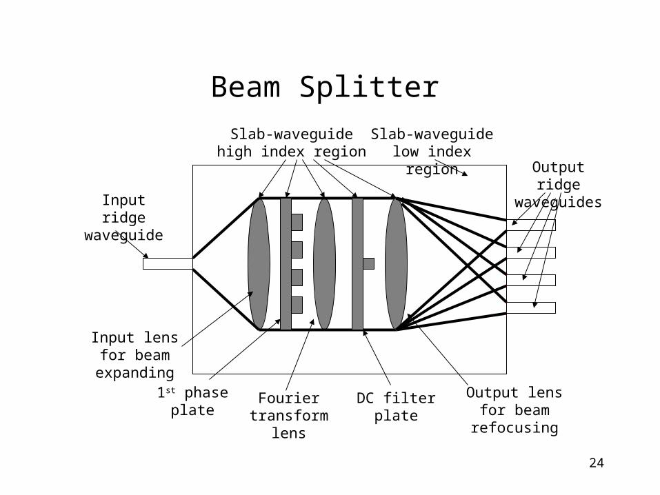
Beam Splitter
Output ridge waveguides
Input ridge waveguide
Slab-waveguide low index region
Slab-waveguide high index region
Input lens for beam expanding
Output lens for beam refocusing
1st phase plate DC filter plateFourier transform lens

25
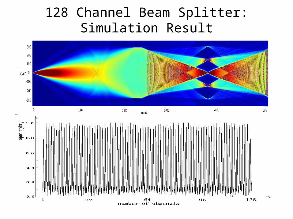
128 Channel Beam Splitter: Design
y
A
L0
L1L2
L5W
z
x
L3G
L4
F
S00
S10
S20
S21
S01
S11
p
Q1 Q2
L4L5
x
z
26
128 Channel Beam Splitter: Simulation Result

27
Polarization Beam Combiner/Splitter

28
Form Birefringence
δ t
Ex
Ey
kz
hl
[ ( ) ] / [ (1 ) ]x h x l x h l xD E t E t f f E
[ / ( ) / ] / [ / (1 ) / ]y y h y l h l yE D t D t f f D
(1 )h lf f
/ [ (1 ) ]h l l hf f

29
Polarization Beam Combiner/SplitterPolarization Beam Combiner/Splitter
• X-pol
• loss:0.633 dB
• Crosstalk35.424dB
• Y-pol
• loss:0.66 dB
• Crosstalk36.029dB
30
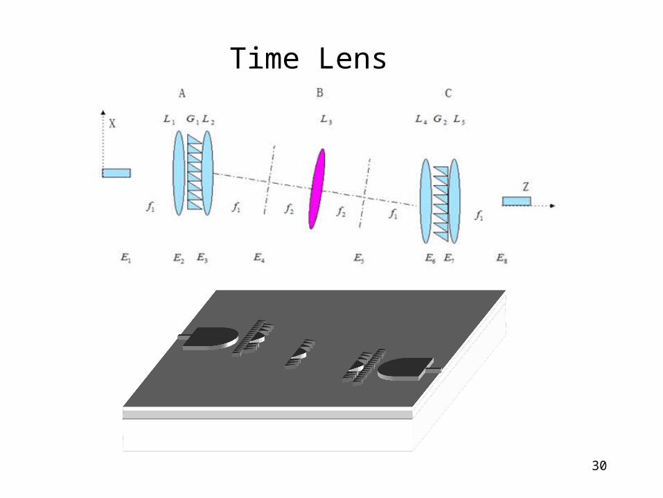
Time Lens

31
Input/Output Simulation Result
Related Documents