1 Clustered Data Cache Designs for VLIW Processors PhD Candidate : Enric Gibert Advisors : Antonio González, Jesús Sánchez

1 Clustered Data Cache Designs for VLIW Processors PhD Candidate: Enric Gibert Advisors: Antonio González, Jesús Sánchez.
Dec 22, 2015
Welcome message from author
This document is posted to help you gain knowledge. Please leave a comment to let me know what you think about it! Share it to your friends and learn new things together.
Transcript

1
Clustered Data Cache Designs for VLIW Processors
PhD Candidate: Enric Gibert
Advisors: Antonio González, Jesús Sánchez

Clustered Data Cache Designs for VLIW ProcessorsEnric Gibert 2
Motivation
• Two major problems in processor design– Wire delays– Energy consumption
Maximum power for INTEL processors
0
20
40
60
80
100
120
PentiumP5
PentiumP54
PentiumMMX
PentiumP6
Pentium II Pentium III Pentium IV
Wat
ts
0
20
40
60
80
100
0,25 0,18 0,13 0,1 0,08 0,06
Processor generation (microns)
D i e
r
e a
c h
a b
l e
( %
)
1 clock
2 clocks
4 clocks
8 clocks
16 clocks
D. Matzke, "Will Physical Scalability Sabotage Performance Gains?¨¨in IEEE Computer 30(9), pp. 37-39, 1997
Maximum power for AMD processors
0
10
20
30
40
50
60
70
80
90
AMD K5 AMD K6 AMD K7 AMD K8
Wat
ts
Data from www.sandpile.org

Clustered Data Cache Designs for VLIW ProcessorsEnric Gibert 3
Clustering
CLUSTER 1
Reg. FileReg. File
FUsFUs
CLUSTER 2
Reg. FileReg. File
FUsFUs
CLUSTER 3
Reg. FileReg. File
FUsFUs
CLUSTER 4
Reg. FileReg. File
FUsFUs
Register-to-register communication buses
L1 cacheL1 cache
L2 cacheL2 cache
Memory buses

Clustered Data Cache Designs for VLIW ProcessorsEnric Gibert 4
Data Cache
• Latency
• Energy– Leakage will soon dominate
energy consumption– Cache memories will probably
be the main source of leakage
ARM1020E dynamic power
I-cache D-cache Instruction MMU BIU Clocks Buffers Core
• In this Thesis:– Latency Reduction Techniques– Energy Reduction Techniques
(S. Hill, Hot Chips 13)
SIA projections
(64KB cache)
100 nm 70nm 50nm 35nm
4 cycles 5 cycles 7 cycles 7 cycles

Clustered Data Cache Designs for VLIW ProcessorsEnric Gibert 5
Contributions of this Thesis
• Memory hierarchy for clustered VLIW processors– Latency Reduction Techniques
• Distribution of the Data Cache among clusters• Cost-effective cache coherence solutions• Word-Interleaved distributed data cache• Flexible Compiler-Managed L0 Buffers
– Energy Reduction Techniques• Heterogeneous Multi-module Data Cache• Unified processors• Clustered processors

Clustered Data Cache Designs for VLIW ProcessorsEnric Gibert 6
Evaluation Framework
• IMPACT C compiler– Compile + optimize + memory disambiguation
• Mediabench benchmark suiteProfile Execution Profile Execution
adpcmdec clinton S_16_44 jpegdec testimg monalisa
adpcmenc clinton S_16_44 jpegenc testimg monalisa
epicdec test_image titanic mpeg2dec mei16v2 tek6
epicenc test_image titanic pegwitdec pegwit techrep
g721dec clinton S_16_44 pegwitenc pgptest techrep
g721enc clinton S_16_44 pgpdec pgptext techrep
gsmdec clinton S_16_44 pgpenc pgptest techrep
gsmenc clinton S_16_44 rasta ex5_c1 ex5_c1
• Microarchitectural VLIW simulator

Clustered Data Cache Designs for VLIW ProcessorsEnric Gibert 7
Presentation Outline
• Latency reduction techniques– Software memory coherence in distributed caches– Word-interleaved distributed cache– Flexible Compiler-Managed L0 Buffers
• Energy reduction techniques– Multi-Module cache for clustered VLIW processor
• Conclusions

Clustered Data Cache Designs for VLIW ProcessorsEnric Gibert 8
Distributing the Data Cache
CLUSTER 1
Reg. FileReg. File
FUsFUs
CLUSTER 2
Reg. FileReg. File
FUsFUs
CLUSTER 3
Reg. FileReg. File
FUsFUs
CLUSTER 4
Reg. FileReg. File
FUsFUs
Register-to-register communication buses
L2 cacheL2 cache
L1 cacheL1 cache
Memory buses
L1 cachemodule
L1 cachemodule
L1 cachemodule
L1 cachemodule

Clustered Data Cache Designs for VLIW ProcessorsEnric Gibert 9
MultiVLIW
CLUSTER 1
Reg. FileReg. File
FUsFUs
CLUSTER 2
Reg. FileReg. File
FUsFUs
CLUSTER 3
Reg. FileReg. File
FUsFUs
CLUSTER 4
Reg. FileReg. File
FUsFUs
Register-to-register communication buses
L1 cachemodule
L1 cachemodule
L1 cachemodule
L1 cachemodule
L2 cacheL2 cache
MSI cache coherence protocol
cache block
(Sánchez and González, MICRO33)

Clustered Data Cache Designs for VLIW ProcessorsEnric Gibert 10
Presentation Outline
• Latency reduction techniques– Software memory coherence in distributed caches
– Word-interleaved distributed cache– Flexible Compiler-Managed L0 Buffers
• Energy reduction techniques– Multi-Module cache for clustered VLIW processor
• Conclusions

Clustered Data Cache Designs for VLIW ProcessorsEnric Gibert 11
Memory Coherence
CLUSTER 1
X
Cache module
CL
US
TE
R 3
CL
US
TE
R 2
CLUSTER 4
Cache module
NEXT MEMORY LEVELNEXT MEMORY LEVEL
memory buses
cycle i - - - store to X
cycle i+1 - - - -
cycle i+2 - - - -
cycle i+3 - - - -
cycle i+4 load from X - - -
new value of Xnew value of X
Update XRead X
new value of Xnew value of X
Remote accessesMissesReplacementsOthers
NON-DETERMINISTIC BUS LATENCY!!!

Clustered Data Cache Designs for VLIW ProcessorsEnric Gibert 12
Coherence Solutions: Overview
• Local scheduling solutions applied to loops– Memory Dependent Chains (MDC)– Data Dependence Graph Transformations (DDGT)
• Store replication• Load-store synchronization
• Software-based solutions with little hardware support
• Applicable to different configurations– Word-interleaved cache– Replicated distributed cache– Flexible Compiler-Managed L0 Buffers

Clustered Data Cache Designs for VLIW ProcessorsEnric Gibert 13
Scheme 1: Mem. Dependent Chains
• Sets of memory dependent instructions– Memory disambiguation by the compiler
• Conservative assumptions
– Assign instructions in same set to same cluster
LD LD
ADD
ST
Registerdeps
Memorydeps
CLUSTER 1
X
cache module
CL
US
TE
R 3
CL
US
TE
R 2
CLUSTER 4
cache module
store to X
load from X
store to X

Clustered Data Cache Designs for VLIW ProcessorsEnric Gibert 14
Scheme 2: DDG transformations (I)
• 2 transformations applied together• Store replication overcome MF and MO
– Little support from the hardware
CLUSTER 1
cache module
CLUSTER 4
cache module
store to X
CLUSTER 2
X
cache module
CLUSTER 3
cache module
store to X store to X
store to X
local instance
remote instances
load from X

Clustered Data Cache Designs for VLIW ProcessorsEnric Gibert 15
load from X
Scheme 2: DDG transformations (II)
• Load-store synchronization overcome MA dependences
LD
ST
add
RF
MA
SYNC
CLUSTER 1
cache module
CL
US
TE
R 2
CLUSTER 3
X
cache module
add
CL
US
TE
R 4
store to X

Clustered Data Cache Designs for VLIW ProcessorsEnric Gibert 16
Results: Memory Coherence
• Memory Dependent Chains (MDC)– Bad since restrictions on the assignment of
instructions to clusters– Good when memory disambiguation is accurate
• DDG Transformations (DDGT)– Good when there is pressure in the memory buses
• Increases number of local accesses
– Bad when there is pressure in the register buses• Big increase in inter-cluster communications
• Solutions useful for different cache schemes

Clustered Data Cache Designs for VLIW ProcessorsEnric Gibert 17
Presentation Outline
• Latency reduction techniques– Software memory coherence in distributed caches– Word-interleaved distributed cache
– Flexible Compiler-Managed L0 Buffers
• Energy reduction techniques– Multi-Module cache for clustered VLIW processor
• Conclusions

Clustered Data Cache Designs for VLIW ProcessorsEnric Gibert 18
Word-Interleaved Cache
• Simplify hardware– As compared to MultiVLIW
• Avoid replication
• Strides +1/-1 element are predominant– Page interleaved– Block interleaved– Word interleaved best suited

Clustered Data Cache Designs for VLIW ProcessorsEnric Gibert 19
Architecture
CLUSTER 1
Register FileRegister File
Func. UnitsFunc. Units
Register-to-register communication buses
cache module
CLUSTER 2
Register FileRegister File
Func. UnitsFunc. Units
cache module
CLUSTER 3
Register FileRegister File
Func. UnitsFunc. Units
cache module
CLUSTER 4
Register FileRegister File
Func. UnitsFunc. Units
cache module
L2 cache
TAG TAG TAG TAGW0 W4 W1 W5 W2 W6 W3 W7
subblock 1local hit
remote hitlocal missTAG W0 W1 W2 W4 W5 W6 W7W3
cache block
remote miss

Clustered Data Cache Designs for VLIW ProcessorsEnric Gibert 20
Instruction Scheduling (I): Unrolling
CLUSTER 1
cache module
a[0] a[4]
for (i=0; i<MAX; i++) { ld r3, @a[i] …}
CLUSTER 2
cache module
a[1] a[5]
CLUSTER 3
cache module
a[2] a[6]
CLUSTER 4
cache module
a[3] a[7]
25% of local accesses
for (i=0; i<MAX; i=i+4) { ld r3, @a[i] ld r3, @a[i+1] ld r3, @a[i+2] ld r3, @a[i+3] …}
ld r3, @a[i]ld r3, @a[i+1]ld r3, @a[i+2]ld r3, @a[i+3]
100% of local accesses

Clustered Data Cache Designs for VLIW ProcessorsEnric Gibert 21
Instruction Scheduling (II)
• Assign appropriate latency to memory instruction– Small latencies ILP ↑, stall time ↑– Large latencies ILP ↓, stall time ↓– Start with large latency (remote miss) + iteratively reassign
appropriate latencies (local miss, remote hit, local hit)
LD
add
RF LD
add
Cluster 1 C2 C3 C4
cycle 1
cycle 2
cycle 3
small latenciesLD
Cluster 1 C2 C3 C4
cycle 1
cycle 2
cycle 3
add
cycle 4
cycle 5
large latencies

Clustered Data Cache Designs for VLIW ProcessorsEnric Gibert 22
Instruction Scheduling (III)
• Assign instructions to clusters– Non-memory instructions
• Minimize inter-cluster communications• Maximize workload balance among clusters
– Memory instructions 2 heuristics• Preferred cluster (PrefClus)
– Average preferred cluster of memory dependent set
• Minimize inter-cluster communications (MinComs)– Min. Comms. for 1st instruction of the memory dependent set
Clustered Data Cache Designs for VLIW ProcessorsEnric Gibert 23
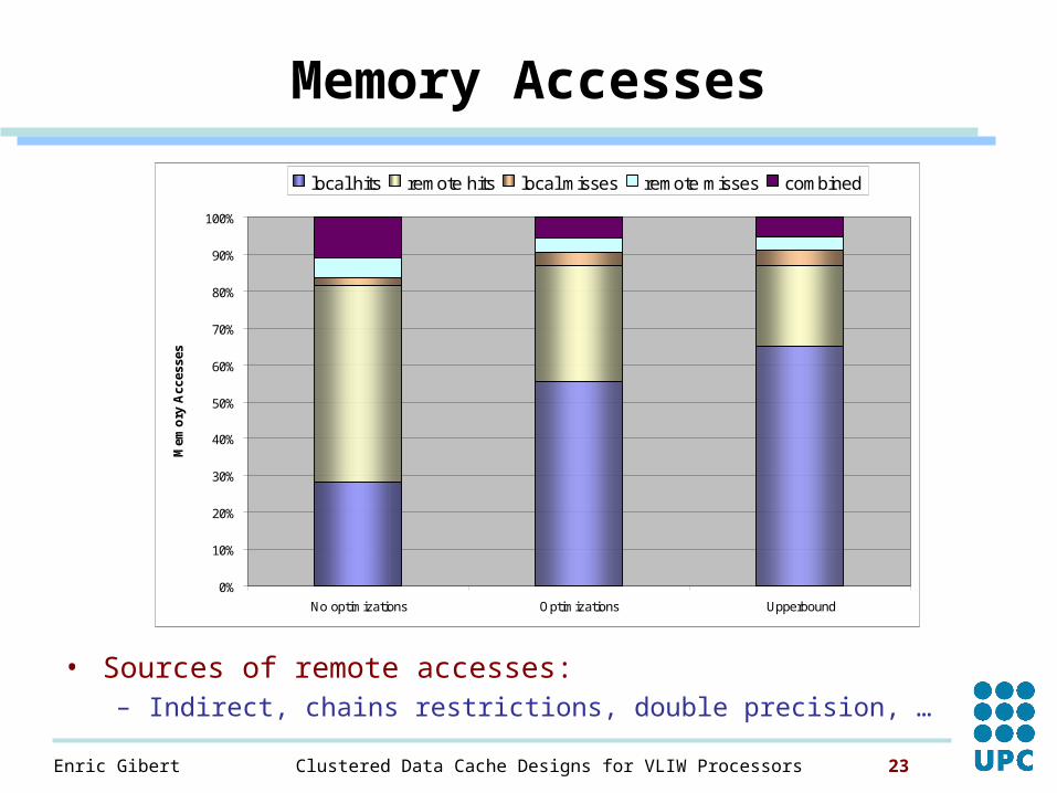
Memory Accesses
• Sources of remote accesses:– Indirect, chains restrictions, double precision, …
0%
10%
20%
30%
40%
50%
60%
70%
80%
90%
100%
No optimizations Optimizations Upperbound
Mem
ory
Acc
esse
slocal hits remote hits local misses remote misses combined

Clustered Data Cache Designs for VLIW ProcessorsEnric Gibert 24
Attraction Buffers
• Cost-effective mechanism ↑ local accesses
CLUSTER 4
a[3] a[7]
cache module
AttractionBuffer
CLUSTER 2
a[1] a[5]
cache module
AB
CLUSTER 3
a[2] a[6]
cache module
AB
CLUSTER 1
a[0] a[4]
cache module
AB
load a[i]i=i+4loop
a[0] a[4]
local accesses0% 50%
• Results– ~ 15% INCREASE in local accesses– ~30-35% REDUCTION in stall time– 5-7% REDUCTION in overall execution time
i=0

Clustered Data Cache Designs for VLIW ProcessorsEnric Gibert 25
Performance
0,750
0,800
0,850
0,900
0,950
1,000
1,050
AVERAGE
Rel
ativ
e E
xecu
tio
n T
ime
Unified Cache
PrefClus
MinComs
MultiVLIW

Clustered Data Cache Designs for VLIW ProcessorsEnric Gibert 26
Presentation Outline
• Latency reduction techniques– Software memory coherence in distributed caches– Word-interleaved distributed cache– Flexible Compiler-Managed L0 Buffers
• Energy reduction techniques– Multi-Module cache for clustered VLIW processor
• Conclusions

Clustered Data Cache Designs for VLIW ProcessorsEnric Gibert 27
Why L0 Buffers
• Still keep hardware simple, but…
• ... Allow dynamic binding between addresses and clusters

Clustered Data Cache Designs for VLIW ProcessorsEnric Gibert 28
L0 Buffers
• Small number of entries flexibility– Adaptative to application + dynamic address-cluster binding
• Controlled by software load/store hints– Mark instructions to access the buffers: which and how
• Flexible Compiler-Managed L0 Buffers
CLUSTER 1
Register FileRegister File
L1 cacheL1 cache
INTINT FPFP MEMMEM
CL
US
TE
R 3
CLUSTER 2
Register FileRegister File
INTINT FPFP MEMMEM
CL
US
TE
R 4
L0 bufferL0 buffer
unpack logic
L0 bufferL0 buffer

Clustered Data Cache Designs for VLIW ProcessorsEnric Gibert 29
Mapping Flexibility
1 2 3 4 5 6 7 8 9 10 11 12 13 14 15 16
a[0]
a[1]
a[2]
a[3]
a[4]
a[5]
a[6]
a[7]
CLUSTER 1
L0 Buffer
L1 block (16 bytes)
L1 cache
CLUSTER 2
L0 Buffer
CLUSTER 3
L0 Buffer
CLUSTER 4
L0 Buffer
1 2 3 4
a[0] a[1]a[0] a[1] a[0] a[1]a[0] a[1]
interleavedmapping
(1 cycle penalty)a[0] a[4] a[1] a[5] a[2] a[6]a[3] a[7]
1 2 3 4 5 6 7 8 9 10 11 12 13 14 15 16
load a[0] load a[1] load a[2]load a[3]All loads with a4-element stride
unpack logic
4 bytes 4 bytes 4 bytes 4 bytes
1 2 3 4
load a[0] with stride 1 element
a[0] a[1]
linearmapping

Clustered Data Cache Designs for VLIW ProcessorsEnric Gibert 30
Hints and L0-L1 Interface
• Memory hints– Access or bypass the L0 Buffers– Data mapping: linear/interleaved– Prefetch hints next/previous blocks
• L0 are write-through with respect to L1– Simplifies replacements– Makes hardware simple
• No arbitration
• No logic to pack data back correctly
– Simplifies coherence among L0 Buffers

Clustered Data Cache Designs for VLIW ProcessorsEnric Gibert 31
Instruction Scheduling
• Selective loop unrolling– No unroll vs. unroll by N
• Assign latencies to memory instructions– Critical instructions (slack) use L0 Buffers– Do not overflow L0 Buffers
• Use counter of L0 Buffer free entries / cluster• Do not schedule critical instruction into cluster with counter == 0
– Memory coherence• Cluster assignment + schedule instructions
– Minimize global communications– Maximize workload balance– Critical Priority to clusters where L0 Buffer can be used
• Explicit prefetching

Clustered Data Cache Designs for VLIW ProcessorsEnric Gibert 32
Number of Entries
0,76
0,78
0,8
0,82
0,84
0,86
0,88
0,9
0,92
0,94
AVERAGE
Rel
ativ
e E
xecu
tio
n T
ime
2 entries
4 entries
8 entries
unbounded entries
4 entries + not selective

Clustered Data Cache Designs for VLIW ProcessorsEnric Gibert 33
Performance
0,75
0,8
0,85
0,9
0,95
1
AVERAGE
Rel
ativ
e E
xecu
tio
n T
ime
L0 Buffers
Interleaved - PrefClus
Interleaved - MinComs
MultiVLIW

Clustered Data Cache Designs for VLIW ProcessorsEnric Gibert 34
Global Comparative
MultiVLIW Word Interleaved
L0 Buffers
Hardware Complexity Lower is better High Low Low
Software Complexity Lower is better Low Medium High
Performance Higher is better High Medium High

Clustered Data Cache Designs for VLIW ProcessorsEnric Gibert 35
Presentation Outline
• Latency reduction techniques– Software memory coherence in distributed caches– Word-interleaved distributed cache– Flexible Compiler-Managed L0 Buffers
• Energy reduction techniques– Multi-Module cache for clustered VLIW processor
• Conclusions

Clustered Data Cache Designs for VLIW ProcessorsEnric Gibert 36
Motivation
• Energy consumption 1st class design goal• Heterogeneity
– ↓ supply voltage and/or ↑ threshold voltage
• Cache memory ARM10– D-cache 24% dynamic energy– I-cache 22% dynamic energy
• Exploit heterogeneity in the L1 D-cache?
processor front-end
processor back-end
processor front-end
processor back-end
structure tuned for performance
structure tuned for energy

Clustered Data Cache Designs for VLIW ProcessorsEnric Gibert 37
Multi-Module Data Cache
FAST CACHEMODULE
SLOW CACHEMODULE
inst PC
L2 D-CACHE
PR
OC
ES
SO
R CRITICALITYTABLE
RO
B
Instruction-Based Multi-Module(Abella and González, ICCD 2003)
STACKSTACK
HEAP DATAHEAP DATA
GLOBAL DATAGLOBAL DATA
STACKSTACK
HEAP DATAHEAP DATA
GLOBAL DATAGLOBAL DATA
FAS
T S
PA
CE
SLO
W S
PA
CE
SP1
SP2
dis
trib
ute
dst
ack
fra
me
s
FASTMODULE
SLOWMODULE
@
load/storequeues
L2 D-CACHE
L1
D-C
AC
HE
Variable-Based Multi-Module
• It is possible to exploit heterogeneity!

Clustered Data Cache Designs for VLIW ProcessorsEnric Gibert 38
Cache Configurations
8KB8KB 8KB8KB
FAST SLOW
L=21 R/W
L=41 R/W
latency x2energy by 1/3
FAST
FU+RF
CLUSTER 1
FU+RF
CLUSTER 2
FAST+NONE
FAST
FU+RF
CLUSTER 1
FAST
FU+RF
CLUSTER 2
FAST+FAST
SLOW
FU+RF
CLUSTER 1
FU+RF
CLUSTER 2
SLOW+NONE
SLOW
FU+RF
CLUSTER 1
SLOW
FU+RF
CLUSTER 2
SLOW+SLOW
FAST
FU+RF
CLUSTER 1
SLOW
FU+RF
CLUSTER 2
FAST+SLOW
FIRSTMODULE
FU
RF
CLUSTER 1
SECONDMODULE
FU
RF
CLUSTER 2
Register buses
L2 D-CACHE

Clustered Data Cache Designs for VLIW ProcessorsEnric Gibert 39
Instr.-to-Variable Graph (IVG)
• Built with profiling information• Variables = global, local, heap
LD1LD1 LD2LD2 ST1ST1 LD3LD3 ST2ST2 LD4LD4 LD5LD5
VAR V1 VAR V2 VAR V3 VAR V4
FIRST SECOND
CACHE
FU+RF
CLUSTER 1
CACHE
FU+RF
CLUSTER 2
LD2
LD1
LD4LD5
ST1
LD3
ST2

Clustered Data Cache Designs for VLIW ProcessorsEnric Gibert 40
Greedy Mapping Algorithm
• Initial mapping all to first @ space• Assign affinities to instructions
– Express a preferred cluster for memory instructions: [0,1]– Propagate affinities to other instructions
• Schedule code + refine mapping
Compute IVG Compute IVG
Compute mappingCompute mappingCompute affinities
+ propagate affinities
Compute affinities + propagate affinities
Schedule codeSchedule code

Clustered Data Cache Designs for VLIW ProcessorsEnric Gibert 41
Computing and Propagating Affinity
add1add1
add2add2
LD1LD1
LD2LD2
mul1mul1
add6add6
add7add7
ST1ST1
add3add3
add4add4
LD3LD3
LD4LD4
add5add5
L=1 L=1 L=1 L=1
L=1 L=1 L=1 L=1
L=1
L=1L=1
L=1
L=3
LD1LD1
LD2LD2
LD3LD3
LD4LD4
ST1ST1
V1V1
V2V2
V4V4
V3V3
FIRST SECOND
AFFINITY=0 AFFINITY=1
FIRSTMODULE
FU
RF
CLUSTER 1
Register buses
SECONDMODULE
FU
RF
CLUSTER 2
AFF.=0.4
slack 0 slack 0 slack 2 slack 2
slack 0slack 0
slack 2slack 2
slack 2slack 0
slack 0
slack 5

Clustered Data Cache Designs for VLIW ProcessorsEnric Gibert 42
Cluster Assignment
• Cluster affinity + affinity range used to:– Define a preferred cluster– Guide the instruction-to-cluster assignment process
• Strongly preferred cluster– Schedule instruction in that cluster
• Weakly preferred cluster– Schedule instruction where global comms. are minimized
IB
IC
Affinity range (0.3, 0.7)≤ 0.3 ≥ 0.7
CACHE
FU+RF
CLUSTER 1
CACHE
FU+RF
CLUSTER 2V1
IA
100
Affinity=0
Affinity=0.9
V2 V3
60 40
Affinity=0.4
ICIC
?
IA
IB

Clustered Data Cache Designs for VLIW ProcessorsEnric Gibert 43
EDD Results
0,6
0,7
0,8
0,9
1
1,1
1,2
1,3
1,4
FAST+NONE
FAST+FAST
FAST+SLOW
SLOW+SLOW
SLOW+NONE
Memory Ports
Sensitive Insensitive
Memory Latency Sensitive FAST+FAST FAST+NONE
Insensitive SLOW+SLOW SLOW+NONE

Clustered Data Cache Designs for VLIW ProcessorsEnric Gibert 44
Other Results
Energy·Delay Results
0,6
0,7
0,8
0,9
1
1,1
1,2
adpc
mde
c
adpc
men
c
epicd
ec
epice
nc
g721
dec
g721
enc
gsm
dec
gsm
enc
jpegde
c
jpegen
c
mpe
g2dec
pegw
itdec
pegw
itenc
pgpd
ec
pgpe
ncra
sta
AMEAN
FAST+NONE
FAST+FAST
FAST+SLOW
SLOW+SLOW
SLOW+NONE
BEST UNIFIED FAST
UNIFIED SLOW
EDD 0.89 1.29 1.25
ED 0.89 1.25 1.07
• ED– The SLOW schemes are better
• In all cases, these schemes are better than unified cache– 29-31% better in EDD, 19-29% better in ED
• No configuration is best for all cases

Clustered Data Cache Designs for VLIW ProcessorsEnric Gibert 45
Reconfigurable Cache Results
• The OS can set each module in one state:– FAST mode / SLOW mode / Turned-off
• The OS reconfigures the cache on a context switch– Depending on the applications scheduled in and scheduled out
• Two different VDD and VTH for the cache
– Reconfiguration overhead: 1-2 cycles [Flautner et al. 2002]
• Simple heuristic to show potential– For each application, choose the estimated best cache configuration
BEST
DISTRIBUTED
RECONFIGURABLE SCHEME
EDD 0.89
(FAST+SLOW)
0.86
ED 0.89
(SLOW+SLOW)
0.86

Clustered Data Cache Designs for VLIW ProcessorsEnric Gibert 46
Presentation Outline
• Latency reduction techniques– Software memory coherence in distributed caches– Word-interleaved distributed cache– Flexible Compiler-Managed L0 Buffers
• Energy reduction techniques– Multi-Module cache for clustered VLIW processor
• Conclusions

Clustered Data Cache Designs for VLIW ProcessorsEnric Gibert 47
Conclusions
• Cache partitioning is a good latency reduction technique
• Cache heterogeneity can be used to exploit energy efficiency
• The best energy and performance efficient scheme is a distributed data cache– Dynamic vs. Static mapping between addresses and clusters
• Dynamic for performance (L0 Buffers)
• Static for energy consumption (Variable-Based mapping)
– Hardware vs. Software-based memory coherence solutions• Software solutions are viable

Clustered Data Cache Designs for VLIW ProcessorsEnric Gibert 48
List of Publications
• Distributed Data Cache Memories– ICS, 2002– MICRO-35, 2002– CGO-1, 2003– MICRO-36, 2003– IEEE Transactions on Computers, October 2005– Concurrency & Computation: practice and experience
• (to appear late ’05 / ’06)
• Heterogeneous Data Cache Memories– Technical report UPC-DAC-RR-ARCO-2004-4, 2004– PACT, 2005

49
Questions…
Related Documents