To learn more about ON Semiconductor, please visit our website at www.onsemi.com Please note: As part of the Fairchild Semiconductor integration, some of the Fairchild orderable part numbers will need to change in order to meet ON Semiconductor’s system requirements. Since the ON Semiconductor product management systems do not have the ability to manage part nomenclature that utilizes an underscore (_), the underscore (_) in the Fairchild part numbers will be changed to a dash (-). This document may contain device numbers with an underscore (_). Please check the ON Semiconductor website to verify the updated device numbers. The most current and up-to-date ordering information can be found at www.onsemi.com. Please email any questions regarding the system integration to [email protected]. Is Now Part of ON Semiconductor and the ON Semiconductor logo are trademarks of Semiconductor Components Industries, LLC dba ON Semiconductor or its subsidiaries in the United States and/or other countries. ON Semiconductor owns the rights to a number of patents, trademarks, copyrights, trade secrets, and other intellectual property. A listing of ON Semiconductor’s product/patent coverage may be accessed at www.onsemi.com/site/pdf/Patent-Marking.pdf. ON Semiconductor reserves the right to make changes without further notice to any products herein. ON Semiconductor makes no warranty, representation or guarantee regarding the suitability of its products for any particular purpose, nor does ON Semiconductor assume any liability arising out of the application or use of any product or circuit, and specifically disclaims any and all liability, including without limitation special, consequential or incidental damages. Buyer is responsible for its products and applications using ON Semiconductor products, including compliance with all laws, regulations and safety requirements or standards, regardless of any support or applications information provided by ON Semiconductor. “Typical” parameters which may be provided in ON Semiconductor data sheets and/or specifications can and do vary in different applications and actual performance may vary over time. All operating parameters, including “Typicals” must be validated for each customer application by customer’s technical experts. ON Semiconductor does not convey any license under its patent rights nor the rights of others. ON Semiconductor products are not designed, intended, or authorized for use as a critical component in life support systems or any FDA Class 3 medical devices or medical devices with a same or similar classification in a foreign jurisdiction or any devices intended for implantation in the human body. Should Buyer purchase or use ON Semiconductor products for any such unintended or unauthorized application, Buyer shall indemnify and hold ON Semiconductor and its officers, employees, subsidiaries, affiliates, and distributors harmless against all claims, costs, damages, and expenses, and reasonable attorney fees arising out of, directly or indirectly, any claim of personal injury or death associated with such unintended or unauthorized use, even if such claim alleges that ON Semiconductor was negligent regarding the design or manufacture of the part. ON Semiconductor is an Equal Opportunity/Affirmative Action Employer. This literature is subject to all applicable copyright laws and is not for resale in any manner.

Welcome message from author
This document is posted to help you gain knowledge. Please leave a comment to let me know what you think about it! Share it to your friends and learn new things together.
Transcript

To learn more about ON Semiconductor, please visit our website at www.onsemi.com
Please note: As part of the Fairchild Semiconductor integration, some of the Fairchild orderable part numbers will need to change in order to meet ON Semiconductor’s system requirements. Since the ON Semiconductor product management systems do not have the ability to manage part nomenclature that utilizes an underscore (_), the underscore (_) in the Fairchild part numbers will be changed to a dash (-). This document may contain device numbers with an underscore (_). Please check the ON Semiconductor website to verify the updated device numbers. The most current and up-to-date ordering information can be found at www.onsemi.com. Please email any questions regarding the system integration to [email protected].
Is Now Part of
ON Semiconductor and the ON Semiconductor logo are trademarks of Semiconductor Components Industries, LLC dba ON Semiconductor or its subsidiaries in the United States and/or other countries. ON Semiconductor owns the rights to a number of patents, trademarks, copyrights, trade secrets, and other intellectual property. A listing of ON Semiconductor’s product/patent coverage may be accessed at www.onsemi.com/site/pdf/Patent-Marking.pdf. ON Semiconductor reserves the right to make changes without further notice to any products herein. ON Semiconductor makes no warranty, representation or guarantee regarding the suitability of its products for any particular purpose, nor does ON Semiconductor assume any liability arising out of the application or use of any product or circuit, and specifically disclaims any and all liability, including without limitation special, consequential or incidental damages. Buyer is responsible for its products and applications using ON Semiconductor products, including compliance with all laws, regulations and safety requirements or standards, regardless of any support or applications information provided by ON Semiconductor. “Typical” parameters which may be provided in ON Semiconductor data sheets and/or specifications can and do vary in different applications and actual performance may vary over time. All operating parameters, including “Typicals” must be validated for each customer application by customer’s technical experts. ON Semiconductor does not convey any license under its patent rights nor the rights of others. ON Semiconductor products are not designed, intended, or authorized for use as a critical component in life support systems or any FDA Class 3 medical devices or medical devices with a same or similar classification in a foreign jurisdiction or any devices intended for implantation in the human body. Should Buyer purchase or use ON Semiconductor products for any such unintended or unauthorized application, Buyer shall indemnify and hold ON Semiconductor and its officers, employees, subsidiaries, affiliates, and distributors harmless against all claims, costs, damages, and expenses, and reasonable attorney fees arising out of, directly or indirectly, any claim of personal injury or death associated with such unintended or unauthorized use, even if such claim alleges that ON Semiconductor was negligent regarding the design or manufacture of the part. ON Semiconductor is an Equal Opportunity/Affirmative Action Employer. This literature is subject to all applicable copyright laws and is not for resale in any manner.

FN
B43060T
2 Mo
tion
SP
M®
45 Series
March 2016
©2016 Fairchild Semiconductor Corporation 1 www.fairchildsemi.comFNB43060T2 Rev.1.1
FNB43060T2 Motion SPM® 45 Series
Features• UL Certified No. E209204 (UL1557)
• 600 V - 30 A 3-Phase IGBT Inverter with Integral GateDrivers and Protection
• Low Thermal Resistance Using Ceramic Substrate
• Low-Loss, Short-Circuit Rated IGBTs
• Built-In Bootstrap Diodes and Dedicated Vs Pins Sim-plify PCB Layout
• Built-In NTC Thermistor for Temperature Monitoring
• Separate Open-Emitter Pins from Low-Side IGBTs forThree-Phase Current Sensing
• Single-Grounded Power Supply
• Isolation Rating: 2000 Vrms / min.
Applications• Motion Control - Home Appliance / Industrial Motor
Related Resources• AN-9084 - Smart Power Module, Motion SPM® 45 H
V3 Series User’s Guilde
• AN-9072 - Smart Power Module Motion SPM® inSPM45H Thermal Performance Information
• AN-9071 - Smart Power Module Motion SPM® inSPM45H Mounting Guidance
• AN-9760 - PCB Design Guidance for SPM®
General DescriptionFNB43060T2 is an advanced Motion SPM® 45 moduleproviding a fully-featured, high-performance inverteroutput stage for AC Induction, BLDC, and PMSMmotors. These modules integrate optimized gate driveof the built-in IGBTs to minimize EMI and losses, whilealso providing multiple on-module protection featuresincluding under-voltage lockouts, over-current shutdown,thermal monitoring of drive IC, and fault reporting. Thebuilt-in, high-speed HVIC requires only a single supplyvoltage and translates the incoming logic-level gateinputs to the high-voltage, high-current drive signalsrequired to properly drive the module's internal IGBTs.Separate negative IGBT terminals are available for eachphase to support the widest variety of control algorithms.
Package Marking and Ordering Information
Figure 1. 3D Package Drawing(Click to Activate 3D Content)
Device Device Marking Package Packing Type Quantity
FNB43060T2 FNB43060T2 SPMAB-C26 Rail 12
FN
B43060T
2 Mo
tion
SP
M®
45 Series
©2016 Fairchild Semiconductor Corporation 2 www.fairchildsemi.comFNB43060T2 Rev.1.1
Integrated Power Functions• 600 V - 30 A IGBT inverter for three-phase DC / AC power conversion (please refer to Figure 3)
Integrated Drive, Protection, and System Control Functions• For inverter high-side IGBTs: gate drive circuit, high-voltage isolated high-speed level shifting
control circuit Under-Voltage Lock-Out Protection (UVLO) Note: Available bootstrap circuit example is given in Figures 15.
• For inverter low-side IGBTs: gate drive circuit, Short-Circuit Protection (SCP)control supply circuit Under-Voltage Lock-Out Protection (UVLO)
• Fault signaling: corresponding to UVLO (low-side supply) and SC faults
• Input interface: active-HIGH interface, works with 3.3 / 5 V logic, Schmitt-trigger input
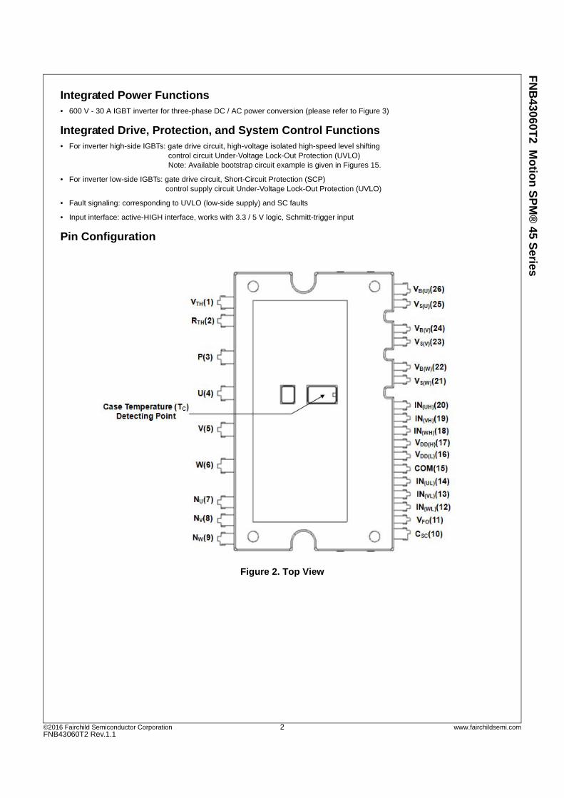
Pin Configuration
Figure 2. Top View

FN
B43060T
2 Mo
tion
SP
M®
45 Series
©2016 Fairchild Semiconductor Corporation 3 www.fairchildsemi.comFNB43060T2 Rev.1.1
Pin Descriptions
Pin Number Pin Name Pin Description
1 VTH Thermistor Bias Voltage
2 RTH Series Resistor for the Use of Thermistor (Temperature Detection)
3 P Positive DC-Link Input
4 U Output for U-Phase
5 V Output for V-Phase
6 W Output for W-Phase
7 NU Negative DC-Link Input for U-Phase
8 NV Negative DC-Link Input for V-Phase
9 NW Negative DC-Link Input for W-Phase
10 CSC Shut Down Input for Short-circuit Current Detection Input
11 VFO Fault Output
12 IN(WL) Signal Input for Low-Side W-Phase
13 IN(VL) Signal Input for Low-Side V-Phase
14 IN(UL) Signal Input for Low-Side U-Phase
15 COM Common Supply Ground
16 VDD(L) Low-Side Common Bias Voltage for IC and IGBTs Driving
17 VDD(H) High-Side Common Bias Voltage for IC and IGBTs Driving
18 IN(WH) Signal Input for High-Side W-Phase
19 IN(VH) Signal Input for High-Side V-Phase
20 IN(UH) Signal Input for High-Side U-Phase
21 VS(W) High-Side Bias Voltage Ground for W-Phase IGBT Driving
22 VB(W) High-Side Bias Voltage for W-Phase IGBT Driving
23 VS(V) High-Side Bias Voltage Ground for V-Phase IGBT Driving
24 VB(V) High-Side Bias Voltage for V-Phase IGBT Driving
25 VS(U) High-Side Bias Voltage Ground for U-Phase IGBT Driving
26 VB(U) High-Side Bias Voltage for U-Phase IGBT Driving
FN
B43060T
2 Mo
tion
SP
M®
45 Series
©2016 Fairchild Semiconductor Corporation 4 www.fairchildsemi.comFNB43060T2 Rev.1.1
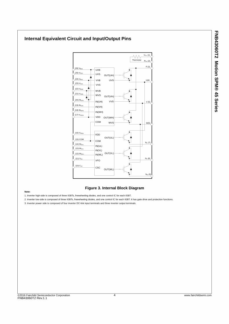
Internal Equivalent Circuit and Input/Output Pins
Figure 3. Internal Block DiagramNote:
1. Inverter high-side is composed of three IGBTs, freewheeling diodes, and one control IC for each IGBT.
2. Inverter low-side is composed of three IGBTs, freewheeling diodes, and one control IC for each IGBT. It has gate drive and protection functions.
3. Inverter power side is composed of four inverter DC-link input terminals and three inverter output terminals.
COM
VDD
IN(WL)
IN(VL)
IN(UL)
VFO
CSCOUT(WL)
OUT(VL)
OUT(UL)
NW (9)
NV (8)
NU (7)
W(6)
V (5)
U(4)
P (3)
(25) VS(U)
(26) VB(U)
(23) VS(V)
(24) VB(V)
(10) CSC
(11) VFO
(12) IN(WL)
(13) IN(VL)
(14) IN(UL)
(15) COM
UVB
OUT(UH)
UVS
IN(UH)
WVS
WVS
OUT(WH)
IN(WH)
COM
VDD
WVB
OUT(VH)
VVS
IN(VH)
VTH (1)
(19) IN(VH)
(20) IN(UH)
(21) VS(W)
(22) VB(W)
(17) VDD(H)
(18) IN(WH)
RTH (2) Thermistor
UVS
VVS
VVB
(16) VDD(L)
FN
B43060T
2 Mo
tion
SP
M®
45 Series
©2016 Fairchild Semiconductor Corporation 5 www.fairchildsemi.comFNB43060T2 Rev.1.1
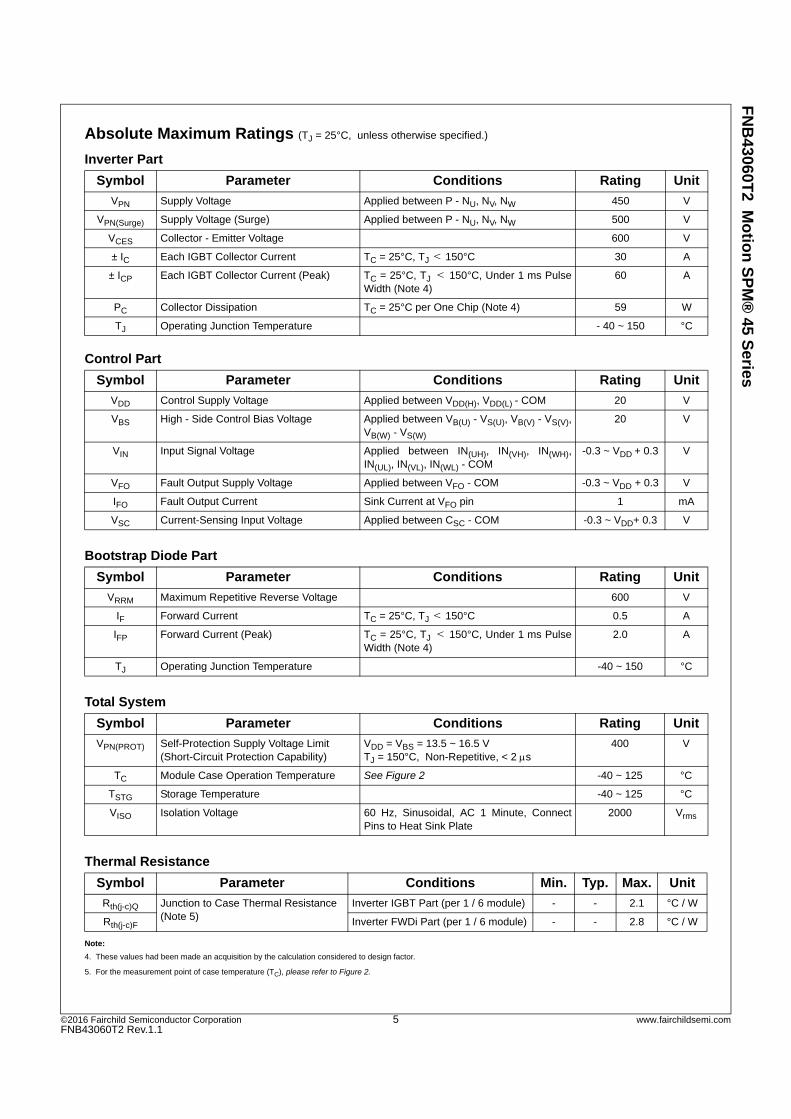
Absolute Maximum Ratings (TJ = 25°C, unless otherwise specified.)
Inverter Part
Control Part
Bootstrap Diode Part
Total System
Thermal Resistance
Note:
4. These values had been made an acquisition by the calculation considered to design factor.
5. For the measurement point of case temperature (TC), please refer to Figure 2.
Symbol Parameter Conditions Rating Unit
VPN Supply Voltage Applied between P - NU, NV, NW 450 V
VPN(Surge) Supply Voltage (Surge) Applied between P - NU, NV, NW 500 V
VCES Collector - Emitter Voltage 600 V
± IC Each IGBT Collector Current TC = 25°C, TJ < 150°C 30 A
± ICP Each IGBT Collector Current (Peak) TC = 25°C, TJ < 150°C, Under 1 ms PulseWidth (Note 4)
60 A
PC Collector Dissipation TC = 25°C per One Chip (Note 4) 59 W
TJ Operating Junction Temperature - 40 ~ 150 °C
Symbol Parameter Conditions Rating Unit
VDD Control Supply Voltage Applied between VDD(H), VDD(L) - COM 20 V
VBS High - Side Control Bias Voltage Applied between VB(U) - VS(U), VB(V) - VS(V),VB(W) - VS(W)
20 V
VIN Input Signal Voltage Applied between IN(UH), IN(VH), IN(WH),IN(UL), IN(VL), IN(WL) - COM
-0.3 ~ VDD + 0.3 V
VFO Fault Output Supply Voltage Applied between VFO - COM -0.3 ~ VDD + 0.3 V
IFO Fault Output Current Sink Current at VFO pin 1 mA
VSC Current-Sensing Input Voltage Applied between CSC - COM -0.3 ~ VDD+ 0.3 V
Symbol Parameter Conditions Rating Unit
VRRM Maximum Repetitive Reverse Voltage 600 V
IF Forward Current TC = 25°C, TJ < 150°C 0.5 A
IFP Forward Current (Peak) TC = 25°C, TJ < 150°C, Under 1 ms PulseWidth (Note 4)
2.0 A
TJ Operating Junction Temperature -40 ~ 150 °C
Symbol Parameter Conditions Rating Unit
VPN(PROT) Self-Protection Supply Voltage Limit(Short-Circuit Protection Capability)
VDD = VBS = 13.5 ~ 16.5 VTJ = 150°C, Non-Repetitive, < 2 s
400 V
TC Module Case Operation Temperature See Figure 2 -40 ~ 125 °C
TSTG Storage Temperature -40 ~ 125 °C
VISO Isolation Voltage 60 Hz, Sinusoidal, AC 1 Minute, ConnectPins to Heat Sink Plate
2000 Vrms
Symbol Parameter Conditions Min. Typ. Max. Unit
Rth(j-c)Q Junction to Case Thermal Resistance(Note 5)
Inverter IGBT Part (per 1 / 6 module) - - 2.1 °C / W
Rth(j-c)F Inverter FWDi Part (per 1 / 6 module) - - 2.8 °C / W

FN
B43060T
2 Mo
tion
SP
M®
45 Series
©2016 Fairchild Semiconductor Corporation 6 www.fairchildsemi.comFNB43060T2 Rev.1.1
Electrical Characteristics (TJ = 25°C, unless otherwise specified.)
Inverter Part
Note:
6. tON and tOFF include the propagation delay time of the internal drive IC. tC(ON) and tC(OFF) are the switching time of IGBT itself under the given gate driving condition internally.For the detailed information, please see Figure 4.
Figure 4. Switching Time Definition
Symbol Parameter Conditions Min. Typ. Max. Unit
VCE(SAT) Collector - Emitter SaturationVoltage
VDD = VBS = 15 VVIN = 5 V
IC = 30 A, TJ = 25°C - 1.65 2.25 V
VF FWDi Forward Voltage VIN = 0 V IF = 30 A, TJ = 25°C - 2.00 2.60 V
HS tON Switching Times VPN = 300 V, VDD = VBS = 15 V, IC = 30 ATJ = 25°CVIN = 0 V 5 V, Inductive Load(Note 6)
0.45 0.85 1.35 s
tC(ON) - 0.20 0.50 s
tOFF - 0.70 1.20 s
tC(OFF) - 0.15 0.45 s
trr - 0.10 - s
LS tON VPN = 300 V, VDD = VBS = 15 V, IC = 30 ATJ = 25°CVIN = 0 V 5 V, Inductive Load(Note 6)
0.5 0.90 1.40 s
tC(ON) - 0.30 0.60 s
tOFF - 0.80 1.30 s
tC(OFF) - 0.15 0.45 s
trr - 0.15 - s
ICES Collector - Emitter LeakageCurrent
VCE = VCES - - 1 mA
VCE IC
VIN
tON
tC(ON)
VIN(ON)
10% IC
10% VCE90% IC
100% IC
trr
100% IC
VCEIC
VIN
tOFF
tC(OFF)
VIN(OFF) 10% VCE 10% IC
(a) turn-on (b) turn-off
FN
B43060T
2 Mo
tion
SP
M®
45 Series
©2016 Fairchild Semiconductor Corporation 7 www.fairchildsemi.comFNB43060T2 Rev.1.1
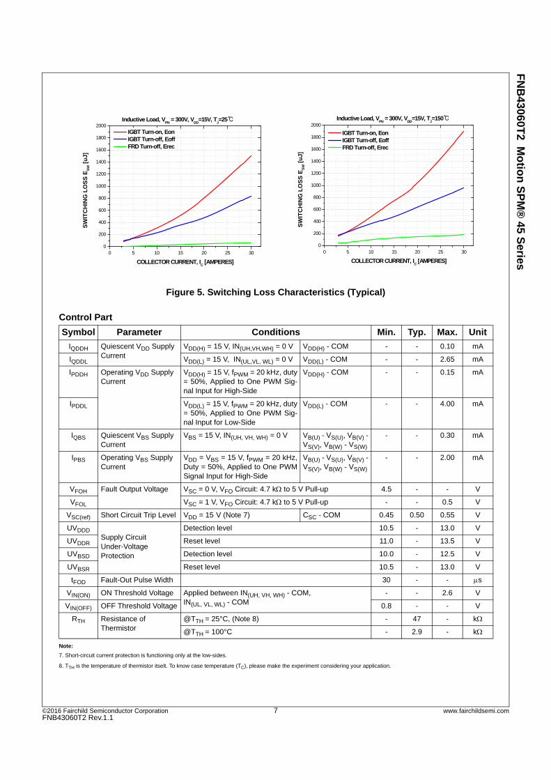
Figure 5. Switching Loss Characteristics (Typical)
Control Part
Note:
7. Short-circuit current protection is functioning only at the low-sides.
8. TTH is the temperature of thermistor itselt. To know case temperature (TC), please make the experiment considering your application.
Symbol Parameter Conditions Min. Typ. Max. Unit
IQDDH Quiescent VDD SupplyCurrent
VDD(H) = 15 V, IN(UH,VH,WH) = 0 V VDD(H) - COM - - 0.10 mA
IQDDL VDD(L) = 15 V, IN(UL,VL, WL) = 0 V VDD(L) - COM - - 2.65 mA
IPDDH Operating VDD SupplyCurrent
VDD(H) = 15 V, fPWM = 20 kHz, duty= 50%, Applied to One PWM Sig-nal Input for High-Side
VDD(H) - COM - - 0.15 mA
IPDDL VDD(L) = 15 V, fPWM = 20 kHz, duty= 50%, Applied to One PWM Sig-nal Input for Low-Side
VDD(L) - COM - - 4.00 mA
IQBS Quiescent VBS SupplyCurrent
VBS = 15 V, IN(UH, VH, WH) = 0 V VB(U) - VS(U), VB(V) -VS(V), VB(W) - VS(W)
- - 0.30 mA
IPBS Operating VBS SupplyCurrent
VDD = VBS = 15 V, fPWM = 20 kHz,Duty = 50%, Applied to One PWMSignal Input for High-Side
VB(U) - VS(U), VB(V) -VS(V), VB(W) - VS(W)
- - 2.00 mA
VFOH Fault Output Voltage VSC = 0 V, VFO Circuit: 4.7 k to 5 V Pull-up 4.5 - - V
VFOL VSC = 1 V, VFO Circuit: 4.7 k to 5 V Pull-up - - 0.5 V
VSC(ref) Short Circuit Trip Level VDD = 15 V (Note 7) CSC - COM 0.45 0.50 0.55 V
UVDDDSupply Circuit Under-Voltage Protection
Detection level 10.5 - 13.0 V
UVDDR Reset level 11.0 - 13.5 V
UVBSD Detection level 10.0 - 12.5 V
UVBSR Reset level 10.5 - 13.0 V
tFOD Fault-Out Pulse Width 30 - - s
VIN(ON) ON Threshold Voltage Applied between IN(UH, VH, WH) - COM, IN(UL, VL, WL) - COM
- - 2.6 V
VIN(OFF) OFF Threshold Voltage 0.8 - - V
RTH Resistance ofThermistor
@TTH = 25°C, (Note 8) - 47 - k
@TTH = 100°C - 2.9 - k
0 5 10 15 20 25 300
200
400
600
800
1000
1200
1400
1600
1800
2000Inductive Load, V
PN = 300V, V
DD=15V, T
J=150
SW
ITC
HIN
G L
OS
S E
SW
[u
J]
COLLECTOR CURRENT, IC [AMPERES]
IGBT Turn-on, Eon IGBT Turn-off, Eoff FRD Turn-off, Erec
0 5 10 15 20 25 300
200
400
600
800
1000
1200
1400
1600
1800
2000
SW
ITC
HIN
G L
OS
S E
SW
[u
J]
COLLECTOR CURRENT, IC [AMPERES]
IGBT Turn-on, Eon IGBT Turn-off, Eoff FRD Turn-off, Erec
Inductive Load, VPN
= 300V, VDD
=15V, TJ=25
FN
B43060T
2 Mo
tion
SP
M®
45 Series
©2016 Fairchild Semiconductor Corporation 8 www.fairchildsemi.comFNB43060T2 Rev.1.1
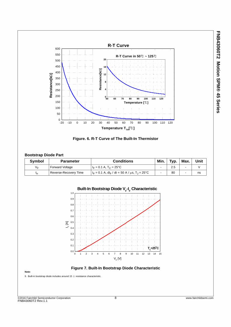
Figure. 6. R-T Curve of The Built-In Thermistor
Bootstrap Diode Part
Figure 7. Built-In Bootstrap Diode CharacteristicNote:
9. Built-in bootstrap diode includes around 15 Ω resistance characteristic.
Symbol Parameter Conditions Min. Typ. Max. Unit
VF Forward Voltage IF = 0.1 A, TC = 25°C - 2.5 - V
trr Reverse-Recovery Time IF = 0.1 A, dIF / dt = 50 A / s, TJ = 25°C - 80 - ns
-20 -10 0 10 20 30 40 50 60 70 80 90 100 110 1200
50
100
150
200
250
300
350
400
450
500
550
600R-T Curve
Res
ista
nce
[k
]
Temperature TTH
[ ]
50 60 70 80 90 100 110 1200
4
8
12
16
20
Res
ista
nc
e[k
]Temperature [ ]
R-T Curve in 50 ~ 125
0 1 2 3 4 5 6 7 8 9 10 11 12 13 14 150.0
0.1
0.2
0.3
0.4
0.5
0.6
0.7
0.8
0.9
1.0
Built-In Bootstrap Diode VF-I
F Characteristic
TC=25oC
I F [
A]
VF [V]
FN
B43060T
2 Mo
tion
SP
M®
45 Series
©2016 Fairchild Semiconductor Corporation 9 www.fairchildsemi.comFNB43060T2 Rev.1.1
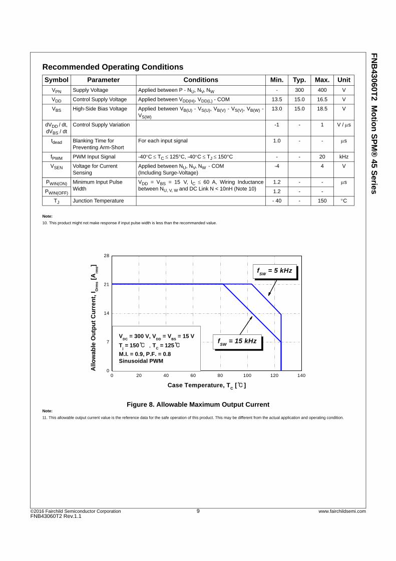
Recommended Operating Conditions
Note:
10. This product might not make response if input pulse width is less than the recommanded value.
Figure 8. Allowable Maximum Output CurrentNote:
11. This allowable output current value is the reference data for the safe operation of this product. This may be different from the actual application and operating condition.
Symbol Parameter Conditions Min. Typ. Max. Unit
VPN Supply Voltage Applied between P - NU, NV, NW - 300 400 V
VDD Control Supply Voltage Applied between VDD(H), VDD(L) - COM 13.5 15.0 16.5 V
VBS High-Side Bias Voltage Applied between VB(U) - VS(U), VB(V) - VS(V), VB(W) -VS(W)
13.0 15.0 18.5 V
dVDD / dt, dVBS / dt
Control Supply Variation -1 - 1 V / s
tdead Blanking Time for Preventing Arm-Short
For each input signal 1.0 - - s
fPWM PWM Input Signal -40C TC 125°C, -40C TJ 150°C - - 20 kHz
VSEN Voltage for CurrentSensing
Applied between NU, NV, NW - COM(Including Surge-Voltage)
-4 4 V
PWIN(ON) Minimum Input PulseWidth
VDD = VBS = 15 V, IC 60 A, Wiring Inductancebetween NU, V, W and DC Link N < 10nH (Note 10)
1.2 - - s
PWIN(OFF) 1.2 - -
TJ Junction Temperature - 40 - 150 C
0 20 40 60 80 100 120 1400
7
14
21
28
VDC
= 300 V, VDD
= VBS
= 15 V
Tj = 150 , T
C = 125
M.I. = 0.9, P.F. = 0.8Sinusoidal PWM
fSW
= 15 kHz
fSW
= 5 kHz
All
ow
able
Ou
tpu
t C
urr
ent,
I Orm
s [
Arm
s]
Case Temperature, TC []

FN
B43060T
2 Mo
tion
SP
M®
45 Series
©2016 Fairchild Semiconductor Corporation 10 www.fairchildsemi.comFNB43060T2 Rev.1.1
Mechanical Characteristics and Ratings
Figure 9. Flatness Measurement Position
Figure 10. Mounting Screws Torque OrderNote:
12. Do not make over torque when mounting screws. Much mounting torque may cause ceramic cracks, as well as bolts and Al heat-sink destruction.
13. Avoid one-sided tightening stress. Figure 10 shows the recommended torque order for mounting screws. Uneven mounting can cause the ceramic substrate of package to be
damaged. The pre-screwing torque is set to 20 ~ 30% of maximum torque rating.
Parameter Conditions Min. Typ. Max. Unit
Device Flatness See Figure 9 0 - + 120 m
Mounting Torque Mounting Screw: M3
See Figure 10
Recommended 0.7 N • m 0.6 0.7 0.8 N • m
Recommended 7.1 kg • cm 6.2 7.1 8.1 kg • cm
Weight - 11.00 - g
1
2Pre - Screwing : 1→2
Final Screwing : 2→1
1
2Pre - Screwing : 1→2
Final Screwing : 2→1

FN
B43060T
2 Mo
tion
SP
M®
45 Series
©2016 Fairchild Semiconductor Corporation 11 www.fairchildsemi.comFNB43060T2 Rev.1.1
Time Charts of Protective Function
Figure 11. Under-Voltage Protection (Low-Side)a1 : Control supply voltage rises: After the voltage rises UVDDR, the circuits start to operate when next input is applied.
a2 : Normal operation: IGBT ON and carrying current.
a3 : Under voltage detection (UVDDD).
a4 : IGBT OFF in spite of control input condition.
a5 : Fault output operation starts with a fixed pulse width.
a6 : Under voltage reset (UVDDR).
a7 : Normal operation: IGBT ON and carrying current by triggering next signal from LOW to HIGH.
Figure 12. Under-Voltage Protection (High-Side)b1 : Control supply voltage rises: After the voltage reaches UVBSR, the circuits start to operate when next input is applied.
b2 : Normal operation: IGBT ON and carrying current.
b3 : Under voltage detection (UVBSD).
b4 : IGBT OFF in spite of control input condition, but there is no fault output signal.
b5 : Under voltage reset (UVBSR).
b6 : Normal operation: IGBT ON and carrying current by triggering next signal from LOW to HIGH.
Input Signal
Output Current
Fault Output Signal
Control Supply Voltage
RESET
UVDDR
Protection Circuit State
SET RESET
UVDDD
a1
a3
a2a4
a6
a5
a7
Input Signal
Output Current
Fault Output Signal
ControlSupply Voltage
RESET
UVBSR
ProtectionCircuit State
SET RESET
UVBSD
b1
b3
b2b4
b6
b5
High-level (no fault output)
FN
B43060T
2 Mo
tion
SP
M®
45 Series
©2016 Fairchild Semiconductor Corporation 12 www.fairchildsemi.comFNB43060T2 Rev.1.1
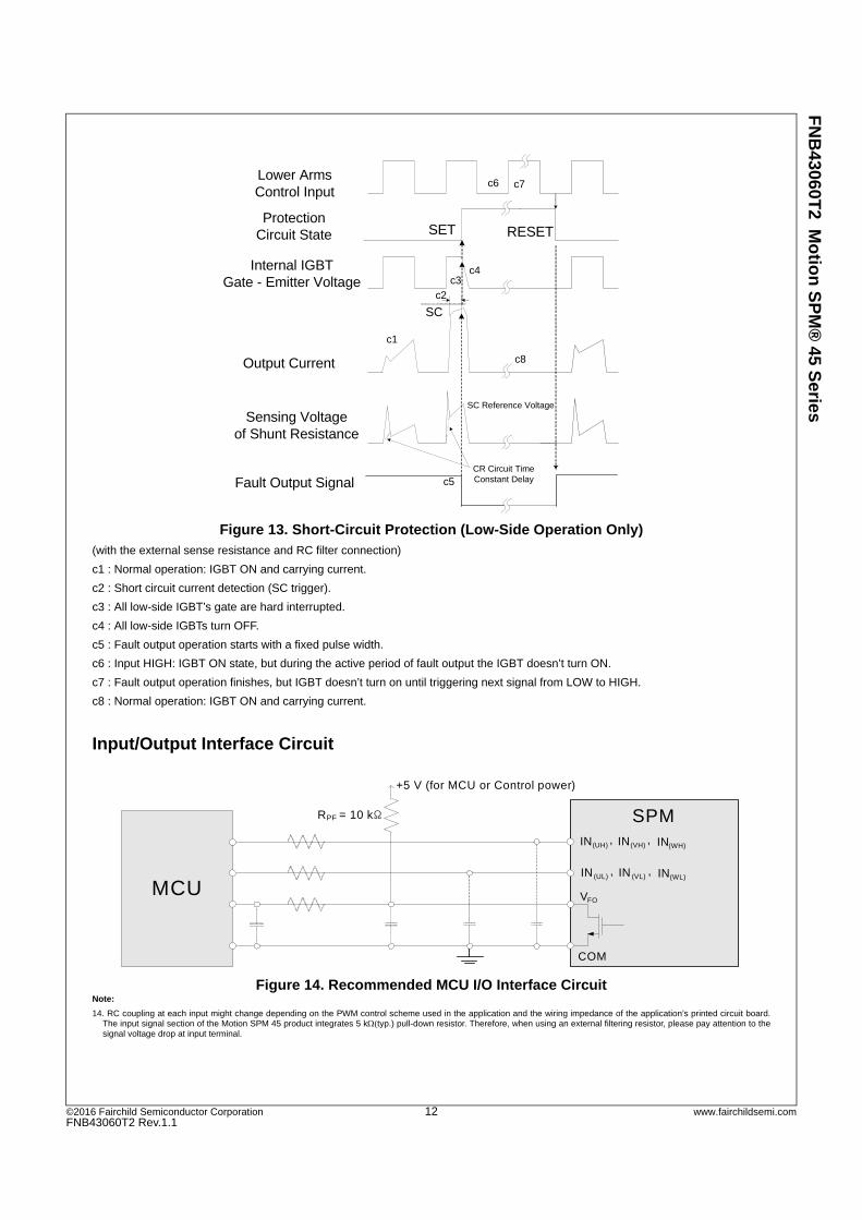
Figure 13. Short-Circuit Protection (Low-Side Operation Only)(with the external sense resistance and RC filter connection)
c1 : Normal operation: IGBT ON and carrying current.
c2 : Short circuit current detection (SC trigger).
c3 : All low-side IGBT’s gate are hard interrupted.
c4 : All low-side IGBTs turn OFF.
c5 : Fault output operation starts with a fixed pulse width.
c6 : Input HIGH: IGBT ON state, but during the active period of fault output the IGBT doesn’t turn ON.
c7 : Fault output operation finishes, but IGBT doesn’t turn on until triggering next signal from LOW to HIGH.
c8 : Normal operation: IGBT ON and carrying current.
Input/Output Interface Circuit
Figure 14. Recommended MCU I/O Interface CircuitNote:
14. RC coupling at each input might change depending on the PWM control scheme used in the application and the wiring impedance of the application’s printed circuit board.The input signal section of the Motion SPM 45 product integrates 5 k(typ.) pull-down resistor. Therefore, when using an external filtering resistor, please pay attention to thesignal voltage drop at input terminal.
Lower Arms Control Input
Output Current
Sensing Voltageof Shunt Resistance
Fault Output Signal
SC Reference Voltage
CR Circuit Time Constant Delay
SC
Protection Circuit State SET RESET
c6 c7
c3
c2
c1
c8
c4
c5
Internal IGBTGate - Emitter Voltage
MCU
COM
+5 V (for MCU or Control power)
, ,IN(UL) IN (VL) IN(WL)
, ,IN(UH) IN(VH) IN(WH)
VFO
RPF = 10 kΩ SPM
FN
B43060T
2 Mo
tion
SP
M®
45 Series
©2016 Fairchild Semiconductor Corporation 13 www.fairchildsemi.comFNB43060T2 Rev.1.1
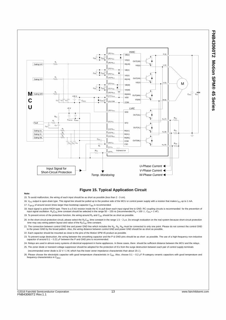
Figure 15. Typical Application CircuitNote:
15. To avoid malfunction, the wiring of each input should be as short as possible (less than 2 - 3 cm).
16. VFO output is open-drain type. This signal line should be pulled up to the positive side of the MCU or control power supply with a resistor that makes IFO up to 1 mA.
17. CSP15 of around seven times larger than bootstrap capacitor CBS is recommended.
18. Input signal is active-HIGH type. There is a 5 k resistor inside the IC to pull down each input signal line to GND. RC coupling circuits is recommanded for the prevention ofinput signal oscillation. RSCPS time constant should be selected in the range 50 ~ 150 ns (recommended RS = 100 Ω , CPS = 1 nF).
19. To prevent errors of the protection function, the wiring around RF and CSC should be as short as possible.
20. In the short-circuit protection circuit, please select the RFCSC time constant in the range 1.5 ~ 2 s. Do enough evaluaiton on the real system because short-circuit protection time may vary wiring pattern layout and value of the RFCSC time constant.
21. The connection between control GND line and power GND line which includes the NU, NV, NW must be connected to only one point. Please do not connect the control GNDto the power GND by the broad pattern. Also, the wiring distance between control GND and power GND should be as short as possible.
22. Each capacitor should be mounted as close to the pins of the Motion SPM 45 product as possible.
23. To prevent surge destruction, the wiring between the smoothing capacitor and the P & GND pins should be as short as possible. The use of a high-frequency non-inductivecapacitor of around 0.1 ~ 0.22 F between the P and GND pins is recommended.
24. Relays are used in almost every systems of electrical equipment in home appliances. In these cases, there should be sufficient distance between the MCU and the relays.
25. The zener diode or transient voltage suppressor should be adopted for the protection of ICs from the surge destruction between each pair of control supply terminals
(recommanded zener diode is 22 V / 1 W, which has the lower zener impedance characteristic than about 15 Ω ).
26. Please choose the electrolytic capacitor with good temperature characteristic in CBS. Also, choose 0.1 ~ 0.2 F R-category ceramic capacitors with good temperature andfrequency characteristics in CBSC.
Fault
+15 V
CBS CBSC
CBS CBSC
CBS CBSC
CSP15 CSPC15
RPF
CBPF
RS
M
VDCCDCS
Gating UH
Gating VH
Gating WH
Gating UL
Gating VL
Gating WL
CPF
MCU
RSW
RSV
RSU
U-Phase Current
V-Phase Current
W-Phase Current
RF
COM
VDD
IN(WL)
IN(VL)
IN(UL)
VFO
CSC
OUT(WL)
OUT(VL)
OUT(UL)
NW (9)
NV (8)
NU (7)
W (6)
V (5)
U (4)
P (3)
(25) VS(U)
(26) VB(U)
(23) VS(V)
(24) VB(V)
(10) CSC
(11) VFO
(14) IN(UL)
(13) IN(VL)
(12) IN(WL)
(20) IN(UH)
(19) IN(VH)
(21) VS(W)
(22) VB(W)
(17) VDD(H)
(18) IN(WH)
Input Signal for Short-Circuit Protection
CSC
RS
RS
RS
RS
RS
RS
CPSCPSCPS
CPSCPS CPS
IN(WH)
IN(VH)
IN(UH)
COM
VDD
VS(W)
VS(V)
VS(U)
VS(V)
VS(U)
VS(W)
VB(U)
VB(V)
VB(W)
(15) COM
OUT(WH)
OUT(VH)
OUT(UH)
LVIC
HVIC
(1) VTH
(2) RTHRTH THERMISTOR
Temp. Monitoring
(16) VDD(L)
+5 V
CSPC05 CSP05

FN
B43060T
2 Mo
tion
SP
M®
45 Series
©2016 Fairchild Semiconductor Corporation 14 www.fairchildsemi.comFNB43060T2 Rev.1.1
Detailed Package Outline Drawings (FNB43060T2)
Package drawings are provided as a service to customers considering Fairchild components. Drawings may change in any manner without notice. Please note the revision and/or data on the drawing and contact a FairchildSemiconductor representative to verify or obtain the most recent revision. Package specifications do not expand the terms of Fairchild’s worldwide therm and conditions, specifically the the warranty therein, which covers Fairchild products.
Always visit Fairchild Semiconductor’s online packaging area for the most recent package drawings:
http://www.fairchildsemi.com/dwg/MO/MOD26AA.pdf

©2016 Fairchild Semiconductor Corporation 15 www.fairchildsemi.comFNB43060T2 Rev.1.1
www.onsemi.com1
ON Semiconductor and are trademarks of Semiconductor Components Industries, LLC dba ON Semiconductor or its subsidiaries in the United States and/or other countries.ON Semiconductor owns the rights to a number of patents, trademarks, copyrights, trade secrets, and other intellectual property. A listing of ON Semiconductor’s product/patentcoverage may be accessed at www.onsemi.com/site/pdf/Patent−Marking.pdf. ON Semiconductor reserves the right to make changes without further notice to any products herein.ON Semiconductor makes no warranty, representation or guarantee regarding the suitability of its products for any particular purpose, nor does ON Semiconductor assume any liabilityarising out of the application or use of any product or circuit, and specifically disclaims any and all liability, including without limitation special, consequential or incidental damages.Buyer is responsible for its products and applications using ON Semiconductor products, including compliance with all laws, regulations and safety requirements or standards,regardless of any support or applications information provided by ON Semiconductor. “Typical” parameters which may be provided in ON Semiconductor data sheets and/orspecifications can and do vary in different applications and actual performance may vary over time. All operating parameters, including “Typicals” must be validated for each customerapplication by customer’s technical experts. ON Semiconductor does not convey any license under its patent rights nor the rights of others. ON Semiconductor products are notdesigned, intended, or authorized for use as a critical component in life support systems or any FDA Class 3 medical devices or medical devices with a same or similar classificationin a foreign jurisdiction or any devices intended for implantation in the human body. Should Buyer purchase or use ON Semiconductor products for any such unintended or unauthorizedapplication, Buyer shall indemnify and hold ON Semiconductor and its officers, employees, subsidiaries, affiliates, and distributors harmless against all claims, costs, damages, andexpenses, and reasonable attorney fees arising out of, directly or indirectly, any claim of personal injury or death associated with such unintended or unauthorized use, even if suchclaim alleges that ON Semiconductor was negligent regarding the design or manufacture of the part. ON Semiconductor is an Equal Opportunity/Affirmative Action Employer. Thisliterature is subject to all applicable copyright laws and is not for resale in any manner.
PUBLICATION ORDERING INFORMATIONN. American Technical Support: 800−282−9855 Toll FreeUSA/Canada
Europe, Middle East and Africa Technical Support:Phone: 421 33 790 2910
Japan Customer Focus CenterPhone: 81−3−5817−1050
www.onsemi.com
LITERATURE FULFILLMENT:Literature Distribution Center for ON Semiconductor19521 E. 32nd Pkwy, Aurora, Colorado 80011 USAPhone: 303−675−2175 or 800−344−3860 Toll Free USA/CanadaFax: 303−675−2176 or 800−344−3867 Toll Free USA/CanadaEmail: [email protected]
ON Semiconductor Website: www.onsemi.com
Order Literature: http://www.onsemi.com/orderlit
For additional information, please contact your localSales Representative
© Semiconductor Components Industries, LLC
Related Documents


![] - H ñ ± æ › _res › projects › default_project › ...KKKKKKKKKKKKKKKKKKKKKK ¢ £ ñ ± P · ï » KKKKKKKK ¢ £ þ q ñ ± & æ ± Ù Ä Ä À KKKKKKKKKKKKKKKKKKKKKK ¬](https://static.cupdf.com/doc/110x72/5f04116b7e708231d40c2904/-h-a-res-a-projects-a-defaultproject-a-kkkkkkkkkkkkkkkkkkkkkk.jpg)


![6× 1Â ] 5ê d dFC).pdfc | 43/1 ¹3L ¿ ² Ä$ AíAþBóBóBòBíBðBðBñBõAí o:w ¹:w"õ:w ¹:w :w Ò:w ¹:w :wBñ:w:w ü:w"á:wBõ:w!ß:wBñ:wBô:w ³$ , $ ã ä 2 Ñ Ñ-~ Ñ!ß](https://static.cupdf.com/doc/110x72/5e407b1c0e1c4f67c12ca38a/6-1-5-d-d-fcpdf-c-431-3l-aabbbbbbbba.jpg)


![Ä Ä Ý vJÄ Ñ B o ÿ % ÿ ) £ g Ï ð h Ä Ä .7 Æ C0& Æ$; ] 6 31 ...yz.tsinghua.edu.cn/.../8549/20181008154428232546906/1538984680087.pdf · Ä Ä " Ý vJÄ Ñ B o ÿ % ÿ](https://static.cupdf.com/doc/110x72/5e1ec4250d013b34012bd451/-vj-b-o-g-h-7-c0-6-31-yz.jpg)