Feb 12, 2002 John Howard, EMC Consultant [email protected] 1 C Z X Y 0 OUTSTANDING IN THE FIELD Electromagnetic Compatibility By Design By A Purveyor of Moderately Dark Magic E Z H X 2 John B. Howard (408) 736-2514 [email protected] www.emcguru.com

Welcome message from author
This document is posted to help you gain knowledge. Please leave a comment to let me know what you think about it! Share it to your friends and learn new things together.
Transcript

Feb 12, 2002 John Howard, EMC [email protected]
1C
Z
X
Y
�
0
OUTSTANDING IN THE FIELD
Electromagnetic Compatibility By DesignBy A Purveyor of Moderately Dark Magic
EZ
H X2�
John B. Howard (408) 736-2514
[email protected] www.emcguru.com

Feb 12, 2002 John Howard, EMC [email protected]
2C
COST EFFECTIVE PCB DESIGN
Some Methods for Minimizing PrintedCircuit Board Electromagnetic Noise

Feb 12, 2002 John Howard, EMC [email protected]
3C
Things Which Cause PCB Cost Explosion
• B. O. M. Worship (Bill Of Materials)– Cheap Parts….penny wise => dollar foolish
• Multiple PCB Spins– Board doesn’t work (excessive pressure on CAD layout)– Creeping Features (who let marketing into the lab?)– Board doesn’t pass EMC (the core of this discussion)
• Anything Relating to Software– I’m a hardware guy; so I blame everything on software

Feb 12, 2002 John Howard, EMC [email protected]
4C
The Sins of Project Management
Ott, Henry W., Noise Reduction Techniques In Electronic Systems, John Wiley & Sons, NY
"Don't worry about EMC now. We'll take care of it later."
"Better call John Howard"
"We can't ship until when?"
EQUIPMENT DEVELOPMENT TIME SCALE
AVAILABLETECHNIQUESANDRELATIVECOSTTO SOLVENOISEPROBLEM
DESIGN PHASE
TESTING PHASE
PRODUCTION PHASE
TECHNIQUES COST

Feb 12, 2002 John Howard, EMC [email protected]
6C
In New Technology Designs…
• The management view of things:– There is a growing gap between “it should work”, and, “it
does work…reliably”. This has led to growing support for Signal Integrity and circuit simulation tools. But focus is really just on getting the design to work.
• But the reality is:– There is a frightening gulf between “it does work”, and, “it
does adequately pass EMC”. EM modeling tools provide needed economical closure of this gulf.

Feb 12, 2002 John Howard, EMC [email protected]
7C
Two Main EM Modeling Camps
• FDTD Finite Difference Time DomainThe field structure of a model is solved for a unique time.Then the process is repeated for a large number of successiveslices of time. This is a time domain approach.
• FEM Finite Element MethodThe model is broken up into tiny elements. The field structure of each element is solved for a unique frequency. The process is repeated for each element of the model. Refinement of the elements then offers increased precision in selected parts of the model. This is a frequency domain approach

Feb 12, 2002 John Howard, EMC [email protected]
8C
A Simple 2D FEM ExampleA 5 mil wide trace positioned 10 mils from the return plane/s
This simple comparison simulation was done at 200 MHz using Ansoft 2D Software (http://www.ansoft.com).
Stripline………Really Good!
Microstrip………Really Bad!
FR-4
FR-4
Air
Return Planes
Return Plane
Radiation

Feb 12, 2002 John Howard, EMC [email protected]
9C
Microstrip Coupling
Notice the dramatic difference in trace to return plane coupling when going from 5 mil thick FR4 to 20 mil thick FR4. The trace is 5 mils wide.
Created with Ansoft 2D Software
FR-4
Air
AirFR-4
Return Plane
Return Plane
Like in a 10 layer PCB
Like in a 4 layer PCB

Feb 12, 2002 John Howard, EMC [email protected]
10C
Let Us Now Use This Information
Ground Plane
Dielectric Core
Dielectric Pre-Preg
Signal Layer
Vcc Plane
Signal Layer
Dielectric Core
This conventional symmetric four layer stack is notable in thatit avoids any emc benefit in all catagories. It does nothing well.
.062"1.575 mm

Feb 12, 2002 John Howard, EMC [email protected]
11C
A Branch Of The Decision Tree
• Modify The PCB Design To Either:Move the power and ground planes closer together to
enhance the interplane capacitance and contribution to circuit bypass capacitance.
• Or:Move the power and ground planes apart to enhance trace-
to-return plane coupling. This can significantly reduce emissions and crosstalk at zero or negligible cost.
• Decide First Which You Most Need

Feb 12, 2002 John Howard, EMC [email protected]
12C
The Usual Better Choice For Small PCB’s
VERY WIDE GROUND TRACE
GROUND PLANE
FR-4 DIELECTRIC
CLOCK TRACE
SIGNAL LAYER
Vcc PLANE Vcc PLANE
SIGNALS SIGNALS
46-48 mils1.17-1.22 mm
62 Mils1.575 mm

Feb 12, 2002 John Howard, EMC [email protected]
13C
But If You Choose This Arrangement
• Emphasize Your Bypass Capacitor Strategy
– On large / fast chips use an array of bycap values for each power pin. Remember, caps are cheap.
– For selected parts, include a filter to isolate the simultaneous switching transient from the planes.
– ALWAYS devote time and effort to minimizing the total loop inductance of each bypass capacitor net.

Feb 12, 2002 John Howard, EMC [email protected]
14C
Examples Of Low Inductance Bycap NetsThe bypass capacitor copper connections are lighter green
Feb 12, 2002 John Howard, EMC [email protected]
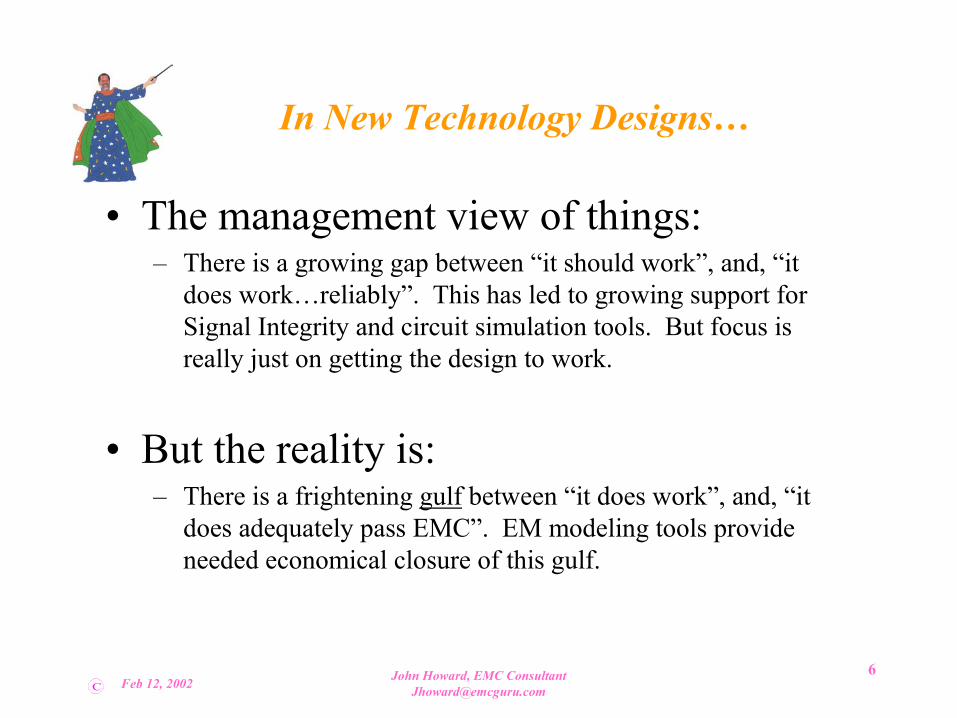
15C
A Suggested Thermal AdjustmentThis 2 GHz simulation shows that the conventional four legged thermal relief pattern should be replaced by a single wide thermal leg directly under the signal trace. This simulation is slightly contrived with the trace isolated from the ground via.

Feb 12, 2002 John Howard, EMC [email protected]
16C
Another Topic
• Know The Expected Energy On Each Net– You mean you don’t know the edge times of each part?
No problem……….just look it up in the spec………….right.
– Since you don’t know the fastest edge times of the parts you plan to use, measure them; then allow for the edge time reduction which will certainly occur from chip die shrink over time.
– Establish a net hierarchy which groups nets according to their expected spectral energy (ie clocks at the highest level and quasistatic signals at the lowest level).
– Plan to route the highest energy nets without layer changes and with careful attention to the assuring tightly coupled return paths.

Feb 12, 2002 John Howard, EMC [email protected]
17C
Route Direction ChangeThis model depicts a common problem faced by CAD layout folks when a orthogonal change in route direction is desired. In a four layer PCB, for example, one simply vias down to the solder side.This picture shows a symmetric stack for a typical 62 mil PCB.

Feb 12, 2002 John Howard, EMC [email protected]
18C
Ground & Power Plane Current At 100 MHz
Component side trace over the ground plane Power plane current distribution
When the trace transitions through the planes at the via, coupling is retained to the adjacent ground plane but seriously lost to the power plane. Skin effect exacerbates this problem because the bottom face of the power plane is even further uncoupled.
Electromagnetic field simulations were done using Ansoft HFSS 8
Feb 12, 2002 John Howard, EMC [email protected]
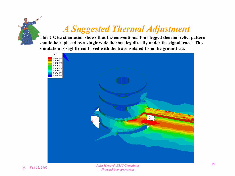
19C
Ground & Power Plane Current At 1 GHz
Component side trace over the ground plane Power plane current distribution
Electromagnetic field simulations were done using Ansoft HFSS 8

Feb 12, 2002 John Howard, EMC [email protected]
20C
Ground & Power Plane Current At 10 GHz
Power plane current distributionComponent side trace over the ground plane
Notice the significant scattering from the via to the power plane when the signal uncouples.
Electromagnetic field simulations were done using Ansoft HFSS 8

Feb 12, 2002 John Howard, EMC [email protected]
21C
Closeup Of The Trace To Via Connection
100 MHz 10 GHz
These closeups of the 8 layer PCB structure show the trace on layer 3 with ground power pair on layers 4 and 5 respectively. Note the very tight coupling between the trace and ground at higher frequency.
Electromagnetic field simulations were done using Ansoft HFSS 8

Feb 12, 2002 John Howard, EMC [email protected]
22C
Some Of The Things To Do
• Create the net hierarchy of signal energy before the CAD layout begins• Use EM simulation tools, if possible, to find problems in the layout• Organize the component topology to minimize microstrip route lengths• In multilayer PCB’s route the high energy traces in stripline• Put as much effort into designing the signal return paths, as the net traces• Route the high energy nets first, without mid-net layer changes• Insure unbroken return plane paths for the high energy traces• Place the bypass capacitor arrays first to minimize their route inductance• Let the CAD person have time to create fills in the bycap nets• Use largest possible drill size for all power /ground connections• Use smallest possible drill size for signal connections• Specify 2 oz. Copper for the power distribution and return planes and
stack them REAL close together

Feb 12, 2002 John Howard, EMC [email protected]
23C
In Conclusion
There is a high analogy between getting ready for final exams in college and getting ready for a final EMC test.
“If you don’t want to take the test again……do the homework”
Thank You
Related Documents