CITY UNIVERSITY OF HONG KONG DEPARTMENT OF PHYSICS AND MATERIALS SCIENCE MASTER OF SCIENCE IN MATERIALS ENGINEERING & NANOTECHNOLOGY RESEARCH REPORT Light trapping in ZnO/CdSe nanowire array solar cells and Molybdenum based structure solar cells by YANG Jingya 52785423 April 2013

Welcome message from author
This document is posted to help you gain knowledge. Please leave a comment to let me know what you think about it! Share it to your friends and learn new things together.
Transcript

CITY UNIVERSITY OF HONG KONG
DEPARTMENT OF
PHYSICS AND MATERIALS SCIENCE
MASTER OF SCIENCE IN MATERIALS ENGINEERING &
NANOTECHNOLOGY
RESEARCH REPORT
Light trapping in ZnO/CdSe nanowire array solar cells and Molybdenum based
structure solar cells
by
YANG Jingya
52785423
April 2013

Light trapping in ZnO/CdSe nanowire array solar cells and Molybdenum based
structure solar cells
by
YANG Jingya
____________________________________
Submitted in partial fulfilment of the
requirements for the degree of
MASTER OF SCIENCE IN MATERIALS ENGINEERING &
NANOTECHNOLOGY
(AP6309 Advanced Research)
from
City University of Hong Kong
April 2013
Project Supervisor : Juan Antonio Zapien

Table of Contents
Abstract ............................................................................................................................................ V
Chapter 1 Introduction ...................................................................................................................... 1
1.1 Solar Cells and photovoltaics .............................................................................................. 1
1.2 FDTD used in solar cell research .................................................................................. 2
1.3 Objectives, scope and limitations of this research ........................................................ 3
Chapter 2 Literature review .............................................................................................................. 5
2.1 Theory of Solar Cells .......................................................................................................... 5
2.2 Nanotechnology strategies for solar cell fabrication ........................................................... 7
2.3 Plasmonic and coherent strategies for solar cell applications ............................................. 8
2.4 Enhanced light trapping from nanowire arrays for Solar Cell applications ...................... 10
Chapter 3 Research Methods .......................................................................................................... 12
3.1 The Maxwell’s Equations .................................................................................................. 12
3.2 Finite Difference Time Domain (FDTD) method, Yee cell ............................................... 13
3.3 Dielectric functions of materials ....................................................................................... 15
Chapter 4 Simulation ...................................................................................................................... 16
4.1 ZnO/CdSe nanowire array structure .................................................................................. 16
4.2 Molybdenum use in Solar Cell .......................................................................................... 17
4.2.1 The Reflection and Transmission of Molybdenum ................................................ 20
4.2.2 The surface plasmon resonance of Molybdenum ................................................... 23
4.3 The outline of the Strategy ................................................................................................ 24
Chapter 5 Result and Discussion..................................................................................................... 29
................................................................................................................................................ 29
5.2 Analysis the absorber of ZnO/CdSe Nanowire array based Solar cells ............................ 31
5.3 Analysis the surface Plasmon Resonance of Molybdenum ............................................... 34
5.4 Analysis and Comparison the Molybdenum based Structure ............................................ 36
Chapter 6 Conclusions .................................................................................................................... 37
References ....................................................................................................................................... 38

List of Figures
Figure 1The structure of CIGS device .................................................................................... 2
Figure 2.The structure and working principle of the solar cell. ............................................. 6
Figure 3. Nanotechnology Fabrication Methods ....................................................................... 8
Figure 4. Plasmonic light trapping nanostructure for thin-film solar cell. ................................ 9
Figure 5. The single cell in FDTD (Yell Cell) ......................................................................... 14
Figure 6. The ZnO/CdSe nanowire array structure. ................................................................ 17
Figure 7. The structure of CIGS and Molybdenum. ................................................................ 18
Figure 8. The structured Molybdenum layer used in CIGS. ................................................... 20
Figure 9. The (n,k) of Molybdenum. ....................................................................................... 21
Figure 10. The (n,k) of CIGS. ................................................................................................. 21
Figure 11. The reflection of Molybdenum layer ..................................................................... 22
Figure 12. The comparison transmission of the Molybdenum22
Figure 13. The hemisphere structure. ...................................................................................... 25
Figure 14. The blazed grating structure with 𝜽𝑩 = 30°. ....................................................... 25
Figure 15. Diffraction at a blazed grating ............................................................................... 26
Figure 16. The blazed grating structure with 𝜽𝑩 = 45° ........................................................ 27
Figure 17. The penentration depth-wavelength curve. ............................................................ 28
Figure 18. The (n,k) of ZnO. ................................................................................................... 29
Figure 19. The (n,k) of CdSe. ................................................................................................. 29
Figure 20. Graph of Spectral Irradiance and Standard spectrum on earth (AM1.5) ............... 30
Figure 21. This is a 3D graph to describe the relationship of energy, AVF and thickness of
nanowire. ......................................................................................................................... 30
Figure 22. The absorption of different ZnO/CdSe nanowire arrays. ....................................... 31
Figure 23. The absorption of ZnO/CdSe nanowire which AVF is different with different
thickness of nanowire. ..................................................................................................... 33
Figure 24. The permittivity of (a) Molybdenum and (b) CIGS. .............................................. 35
Figure 25. The absorption of structured Molybdenum used in CIGS. .................................... 36

V
Abstract
FDTD is very useful simulation software can simulate the real situation, which is
widely used in solar cell investigation. In order to investigate the ways to improve the
absorption of solar cells, the research is divided into two parts. One is study factors
influence on the performance of ZnO/CdSe nanowire arrays, the structure is
hexagonal prism, inner core is ZnO, and outer shell is CdSe. There are two variables
can effect on the performance of absorber, thickness and volume fraction. By compare
the absorption of the absorber layer, the ZnO/CdSe nanowire array with 24nm
thickness and 0.20 volume fraction shows the best performance. The other part is to
study the Surface Plasmon Polaraztion of Molybdenum, Mo as a metal, should have
the properties, but results shows that on the visible light wavelength, the Molybdenum
do not have SPP performance. In order to investigate influence of the structured
Molybdenum on absorption of CIGS in solar cell, there are four groups of structures
have been test, the Mo layer is 500nm, the CIGS layer is 100nm which selected
according to the penetration depth. All the groups with structures compare to the no
structured layer can proved that the absorption of CIGS increased, and the MO with
etching sphere structures has the best performance in the four groups.

VI
Acknowledgements
I would like to express my sincere gratitude to Professor J.A.Zapien for his
supervision and guidance in this research project. His invaluable comments and kind
supports helped me to overcome the problems I had to face during my master study
period. I would also like to thank Professor Wu for providing an opportunity for me to
research in advanced level.
My appreciation also goes to my group members, without their assistance, this project
cannot be done smoothly and efficiently.
Financial support for this project was received from the Research Grants Council of
the Hong Kong Special Administrative Region, China (Project No. CityU 103409).

1
Chapter 1 Introduction
1.1 Solar Cells and photovoltaics
As an increasing realization non-renewable energy shortages, scientists and
engineers pay more attention on the the application of new energy, especially
clean renewable sources like solar energy resources, the solar energy technologies
and the application of solar energy have revolutionary breakthrough in recent
years [1]. Solar cells and photovoltaics are a kind of devices that can convert the
energy of sunlight into direct current electricity by using semiconductors. Solar
cells can be divided into three categories: (1) inorganic cells, based on solid-state
inorganic semiconductors; (2) organic cells, based on organic semiconductors; (3)
photoelectrochemical (PEC) cells [2]. Conventionally, the study of the solar cell is
focused on using the n-type material to cover on the p-type silicon and contact
with metals to increase the absorption and increase the energy conversion
efficiency.
As a typical material used in solar cells, silicon is the second most abundant
element in the earth’s crust, silicon is a relatively inexpensive raw material.
However, silicon used as semiconductor such as crystal silicon is very expensive.
As silicon is indirect bandgap semiconductor, high absorption efficiency in
silicon needs relatively large thickness. Therefore, many researchers change the
inner structures and texture of silicon to improve the light path in order to
2
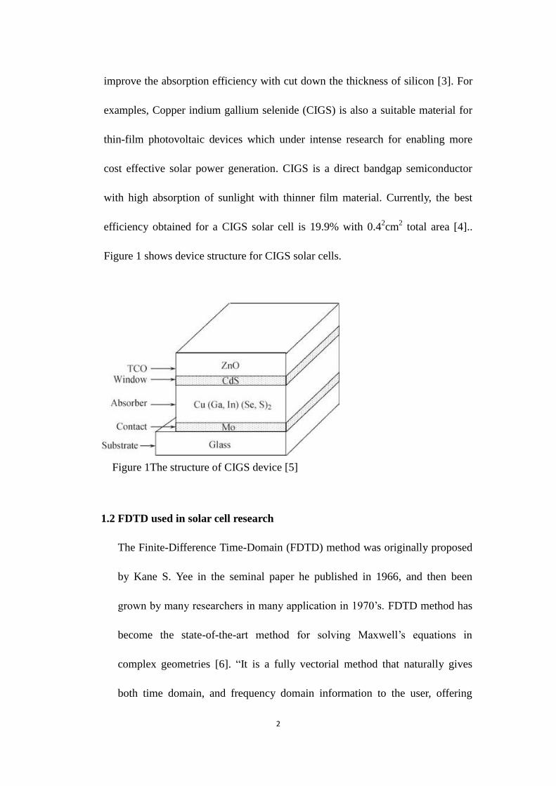
improve the absorption efficiency with cut down the thickness of silicon [3]. For
examples, Copper indium gallium selenide (CIGS) is also a suitable material for
thin-film photovoltaic devices which under intense research for enabling more
cost effective solar power generation. CIGS is a direct bandgap semiconductor
with high absorption of sunlight with thinner film material. Currently, the best
efficiency obtained for a CIGS solar cell is 19.9% with 0.42cm
2 total area [4]..
Figure 1 shows device structure for CIGS solar cells.
Figure 1The structure of CIGS device [5]
1.2 FDTD used in solar cell research
The Finite-Difference Time-Domain (FDTD) method was originally proposed
by Kane S. Yee in the seminal paper he published in 1966, and then been
grown by many researchers in many application in 1970’s. FDTD method has
become the state-of-the-art method for solving Maxwell’s equations in
complex geometries [6]. “It is a fully vectorial method that naturally gives
both time domain, and frequency domain information to the user, offering
3
unique insight into all types of problems and applications in electromagnetics
and photonics” [7]. There are also many other numerical solutions, such as the
Finite Element Method (FEM), Coupled Wave Analysis (RCWA), dipole
approx., etc.. However, FDTD is the most commonly numerical solution, the
advantages of this method is are: (Ⅰ) it does not require the solution to a large
set of linear equations; (Ⅱ ) it can be parallelized to be executed on
high-performance low-cost graphical processing hardware; (Ⅲ) it provides a
broad-band simulation, so that a broad frequency response can be analyzed via
a single simulation; (Ⅳ) it can deal with arbitrary geometry structure. The
distinct disadvantage of FDTD is that spectrally resolved complex refractive
indices of the semiconductor materials, as determined experimentally, cannot
be directly incorporated into the simulation [8].
1.3 Objectives, scope and limitations of this research
Part A Objectives for ZnO/CdSe nanowire arrays Solar Cells
(1) Investigate the optical absorption and optimal geometry in arrays of
ZnO/CdSe nanowires.
(2) Measure the light trapping properties of the ZnO/CdSe nanowire arrays.
(3) Compare the absorption coefficiency and properties of light trapping of
different ZnO/CdSe nanowire arrays and. Find out their respective advantages.
Part B Objectives for Molybdenum Solar Cells
(1) Investigate the MO-based structure for maximum reflection.
4
(2) Measure the light reflection efficiency of Mo-based structure.
(3) Investigate the Surface Plasmon Polaritons (SPP) of Molybdenum structure or
the enhanced scattering structured of Molybdenum structure.
The application areas of FDTD are numerous: electromagnetics, biomedical
engineering, ground penetrating radar, photonics, plasmonics, photovoltaics,
nano-optical storage devices. In this research, the FDTD is applied to investigate the
properties of photovoltaics [9].
The method is not without weakness, such as the FDTD method needs a full
discretization of the electric and magnetic fields throughout the entire volume domain.
Even there are weaknesses of FDTD method, the results will not be affected a lot, and
the results are worth convincing.
5
Chapter 2 Literature review
2.1 Theory of Solar Cells
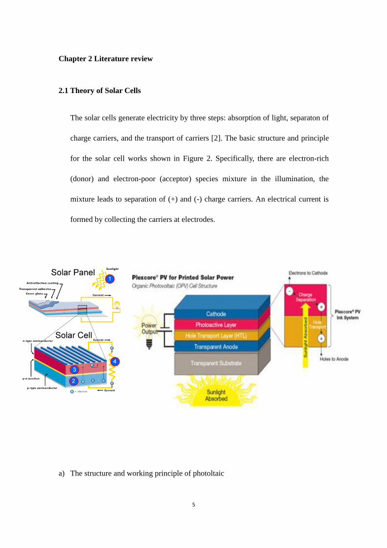
The solar cells generate electricity by three steps: absorption of light, separaton of
charge carriers, and the transport of carriers [2]. The basic structure and principle
for the solar cell works shown in Figure 2. Specifically, there are electron-rich
(donor) and electron-poor (acceptor) species mixture in the illumination, the
mixture leads to separation of (+) and (-) charge carriers. An electrical current is
formed by collecting the carriers at electrodes.
a) The structure and working principle of photoltaic

6
b) The working principle of the solar cell
Figure 2.The structure and working principle of the solar cell. a) The structure and
working principle of photoltaic [10-11]; b) The working principle of the solar cell [12]
To improve the efficiency of solar cells, the absorption efficiency and energy
conversion efficiency are the two important points. The absorption efficiency is
determined by the absorption coefficient of the material which depends on the
material property and the wavelength of light. The absorption coefficient can
determine the length of light path properties through the material; light is highly
absorbed faster in materials with high absorption coefficient. The energy conversion
efficiency depends on the photons, only photons with energy higher than the band gap
can be converted in to electricity, the other photons will pass through the material.
Besides, reduce the reflection and transmission losses are also important to energy
converse efficiency.
7
In order to enhance light absorption in solar technologies without increasing cost,
scientists pay attention on geometrical optical techniques, such as cell texturing and
anti-reflection coatings [13]. These methods can increase the optical path length,
especially applied in the nanostructured material. The grating and photonic crystal can
increase the time of photons in the active solar cell region, so that more photons can
be absorbed. It has been proved that the wire arrays can reduced the reflection of the
photovoltaics by decrease the dielectric mismatch between the material and air, and
can increase the light trapping in the solar cells. Moreover, the method increases the
defect tolerance which result that the material species increased. These methods also
can decrease the cost of production. Due to the advantages as above shown, the design
nanostructured material technologies are promising.
2.2 Nanotechnology strategies for solar cell fabrication
With the increasing demand of thin-film photovoltaics, the nanostructured materials
are being applied in the photovoltaics. There are three advantages of the
nanostructured layer in the thin-film photovoltaics: first, the optical path length can be
increased for the multiple reflections; second, the path of the electrons and holes need
to travel over is shorter which can reduce the recombination losses, as a result, the
absorber layer thickness in nano-structured solar cells can be as thin as 150 nm
instead of several micrometers in the traditional thin film solar cells; third, the energy
band gap of various layers can be tailored to the desired design value by varying the

8
size of nano-particles. This allows for more design flexibility in the absorber and
window layers in the solar cell [14]. Figure 3 shows the different nanotechnologies
used in fabrication.
Figure 3. Nanotechnology Fabrication Methods [15]
2.3 Plasmonic and coherent strategies for solar cell applications
As crystalline silicon wafers with high absorption efficiency all have relatively large
thickness, the price of the solar cell is high. Therefore, the researchers have great
interest on the thin-film solar cells which thickness range is about 1-2 μm. The thick
Si solar cells using the pyramidal surface texture to achieve the light trapping, this
method is not suitable for thin-film solar cell. Researchers use metallic nanostructured
supporting surface plasmons to achieve the light trapping in thin-film solar cells.
Plasmons exist mainly in metals, where electrons are weakly bound and free to roam.
9
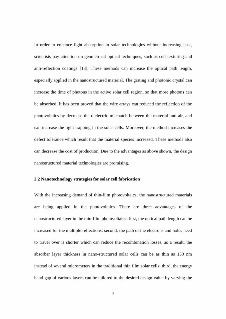
Three different concepts of plasmonic nanostructure integration for solar cells can
reduce the material thickness while keep the absorber layer thickness. First, metal
nanoparticles placed on the surface of solar cell scatter the incident sunlight into solar
cell and couple the light in to guided mode in the solar cell. Then the light scattered to
the high-index substrate, enhance the coupling to the semiconductor. Meanwhile, the
antireflection effect can increase the optical path length, increasing the probability of
light trapping. The process is like folding the light in a thin absorb layer (Fig.4a).
Second, nanoparticles placed in the interface of solar cell, the incident sunlight in the
plasmonic near-field is coupled to the semiconductor, increase the absorption
cross-section (Fig.4b). Third, the patterned metal back contact of a thin-film solar cell
can couple the sunlight into the guided modes in the semiconductor and the surface
plasmon polariton (SPP) mode support at the metal/semiconductor interface, so that
light is guided and absorbed in the plane then converted to carriers in the
semiconductor. Light also will have some loss in the cladding layers [16].
Figure 4. Plasmonic light trapping nanostructure for thin-film solar cell. (a) Light
trapping by scattering from metal nanoparticle placed on the surface of the solar cell. (b)

10
Light trapping by the excitation of localized surface plasmons in metal nanoparticles
embedded in the semiconductor. (c) Light trapping by the excitation of surface plasmon
polaritons at the metal back surface. [16]
Coherent light trapping methods are the approach under research to enhance the
optical absorption by exploiting the wave nature of light in thin-film solar cells. This
is a method that based on light treated as a wave phenomenon, therefore interfere at
the electric field can occur in some regions. [17]
2.4 Enhanced light trapping from nanowire arrays for Solar Cell applications
Thin-film layer uses small amounts of materials for both cheap and expensive, which
is relatively cheaper than the silicon solar cells which have the same absorption
coeffeciency. In addition, thin film can reduce the cost of fabrication by using the the
substrate and semiconductor, but will shorter the optical path length and minority
carrier diffusion length. Therefore, increase the absorption coefficient and light
trapping ability are important. It has been shown that the nanowire array in solar cell
have relatively lower reflection. Erik Garnett have demonstrate that ordered arrays of
silicon nanowires increase the path length of incident solar radiation by up to a factor
of 73. They can get larger area silicon nanowire radial p-n junction photovoltaics by
dip coating a silicon substrate to self-assemble silica sphere, DRIE to form nanowires
and diffusion to form the p-n junction. They achieved efficiencies of between 5 and 6%

11
for these ordered vertical silicon nanowire array solar cells on 20 and 8 μm silicon
absorber layers with different roughness factors. Compare the two groups output
characteristics, it is shown 8 μm thin silicon with the better light-trapping effect which
have the longer nanowires lead to both higher absorption and increased surface
recombination, even without any surface passivation. These nanowire devices give
efficiencies above 5%, with shortcircuit photocurrents higher than planar control
samples [18].
12
Chapter 3 Research Methods
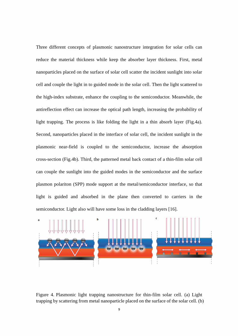
3.1 The Maxwell’s Equations
Table 1. The basic Maxwell’s Equations use in FDTD [19]
The basic Maxwell’s Equations are shown in the Table 1. They describe
how electric and magnetic fields are generated and their interaction with matter.
Gauss law describes the relationship between the electric flux through the arbitrary
closed surface and the charge the closed surface. Gauss’ Law for magnetism describes
the number of the magnetic flux which go through the closed surface is zero.
Faraday's law describes how a time varying magnetic field creates an electric field.
Ampère's law with Maxwell's correction describes how a time varying electric field
and current create the magnetic field.
13
FDTD Solutions can solve the two and three dimensional Maxwell's equations in
dispersive media and some simple non-linear media [20]. For instance, Maxwell
equations have six electromagnetic field components in three dimensions: Ex, Ey,
Ez and Hx, Hy, and Hz. If we assume that the structure is infinite in the z dimension
and that the fields are independent of z, specifically that
Then, the Maxwell’s equations split into TE (transverse electric), and TM (transverse
magnetic) equations, the vector quantities of TE are Ex, Ey, Hz, the vector quantities
of TM are Hx, Hy, Ez, the two sets of equations can be solved in the x-y plane.
3.2 Finite Difference Time Domain (FDTD) method, Yee cell
The Finite-Difference Time-Domain (FDTD) method is the most common numerical
method for solving the Maxwell equations for nanostructured photovoltaic devices.
FDTD discretizes the spatial derivatives of differential operators in the Maxwell
equations by expanding the field on a regular tensorial grid and integrates the
temporal derivatives by time-stepping [21-22]
The simulation space grid and wave can be split into electric wave (TE) and magnetic
wave (TM), E-field is time stepping and estimated instantly varying from H-field by
14
Maxwell’s Equation, H-field is estimated by the changed of E-field and H-field value ,
the relationship of E-field and H-field shown below[23].
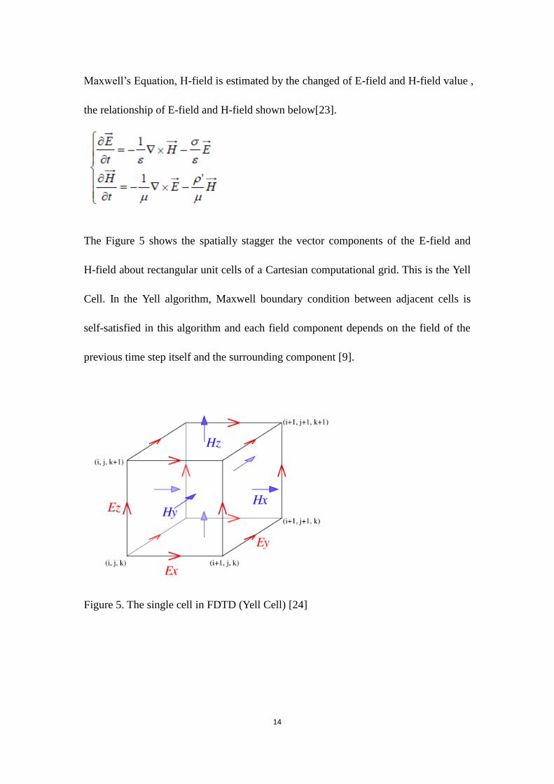
The Figure 5 shows the spatially stagger the vector components of the E-field and
H-field about rectangular unit cells of a Cartesian computational grid. This is the Yell
Cell. In the Yell algorithm, Maxwell boundary condition between adjacent cells is
self-satisfied in this algorithm and each field component depends on the field of the
previous time step itself and the surrounding component [9].
Figure 5. The single cell in FDTD (Yell Cell) [24]

15
3.3 Dielectric functions of materials
The dielectric function of a material stand for the changes of the electrical and optical
properties with the wavelength, energy and etc.. By using the dielectric function,
especially from the relationship between photon and phonon, which describes the
polariton band gap, the polarization and absorption properties of the material can be
observed. The property modifies the electromagnetic wave of light is the dielectric
function ε which consists of two parts ε1 and ε2, or e1 and e2.
The complex dielectric function is:
ε(λ) = e1(λ) ± ie2(λ)
e2 can be a positive quantity, or a negative quantity, so the equation above contains ±
to cover either case.
The e1 and e2 can affect each other, which means the shape of e2 cause corresponding
changes in the shape of e1 and vice-versa.
The dielectric function is related to the refractive index of a material by the
equation ε = n2
Or as complex numbers: (ε1 ± iε2) = (n ± ik)2 [25]
16
Chapter 4 Simulation
4.1 ZnO/CdSe nanowire array structure
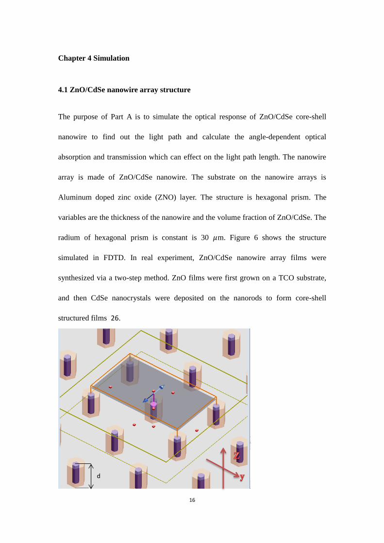
The purpose of Part A is to simulate the optical response of ZnO/CdSe core-shell
nanowire to find out the light path and calculate the angle-dependent optical
absorption and transmission which can effect on the light path length. The nanowire
array is made of ZnO/CdSe nanowire. The substrate on the nanowire arrays is
Aluminum doped zinc oxide (ZNO) layer. The structure is hexagonal prism. The
variables are the thickness of the nanowire and the volume fraction of ZnO/CdSe. The
radium of hexagonal prism is constant is 30 𝜇m. Figure 6 shows the structure
simulated in FDTD. In real experiment, ZnO/CdSe nanowire array films were
synthesized via a two-step method. ZnO films were first grown on a TCO substrate,
and then CdSe nanocrystals were deposited on the nanorods to form core-shell
structured films 26.
d

17
Figure 6. The ZnO/CdSe nanowire array structure.
4.2 Molybdenum use in Solar Cell
To investigate the influence of Molybdenum usd in the CIGS, it is necessary to
investigate the influence of the structures on optical properties of solar cell such as
reflection, diffraction, and so on.
It is desiged a CIGS with Molybdenum back contact. The Molybdenum layer is
500nm, the wavelength range of light sourec is from 300nm to 1100nm. It is
designed four kinds of sturctured Molybdenum. The different size structures are
palced on the Molybdenum layer. Then simulate the structure under suitable
conditions to get the optical propertis of Molybdenum. The Figure 7 shows the
structure of CIGS with Molybdenum and the structure of Molybdenum. They are
simply single layers. The Figure 8 shows the different sturectured Molybdenum.
Generally, the thickness of CIGS is over 1.3 𝜇m while I used 100nm CIGS layer.
Marika demonstrate that quantum efficiency measurements of devices with CIGS
thickness of slightly less than 1 𝜇m indicate that the absorption losses are low, while
Reducing the CIGS thickness to half its present value reduces the total module cost by
about 7.5% according to production cost analysis made within the EUproject LARCIS
[27]. Therefore, it is expected to use sturctured Mo to be the back contact to keep te
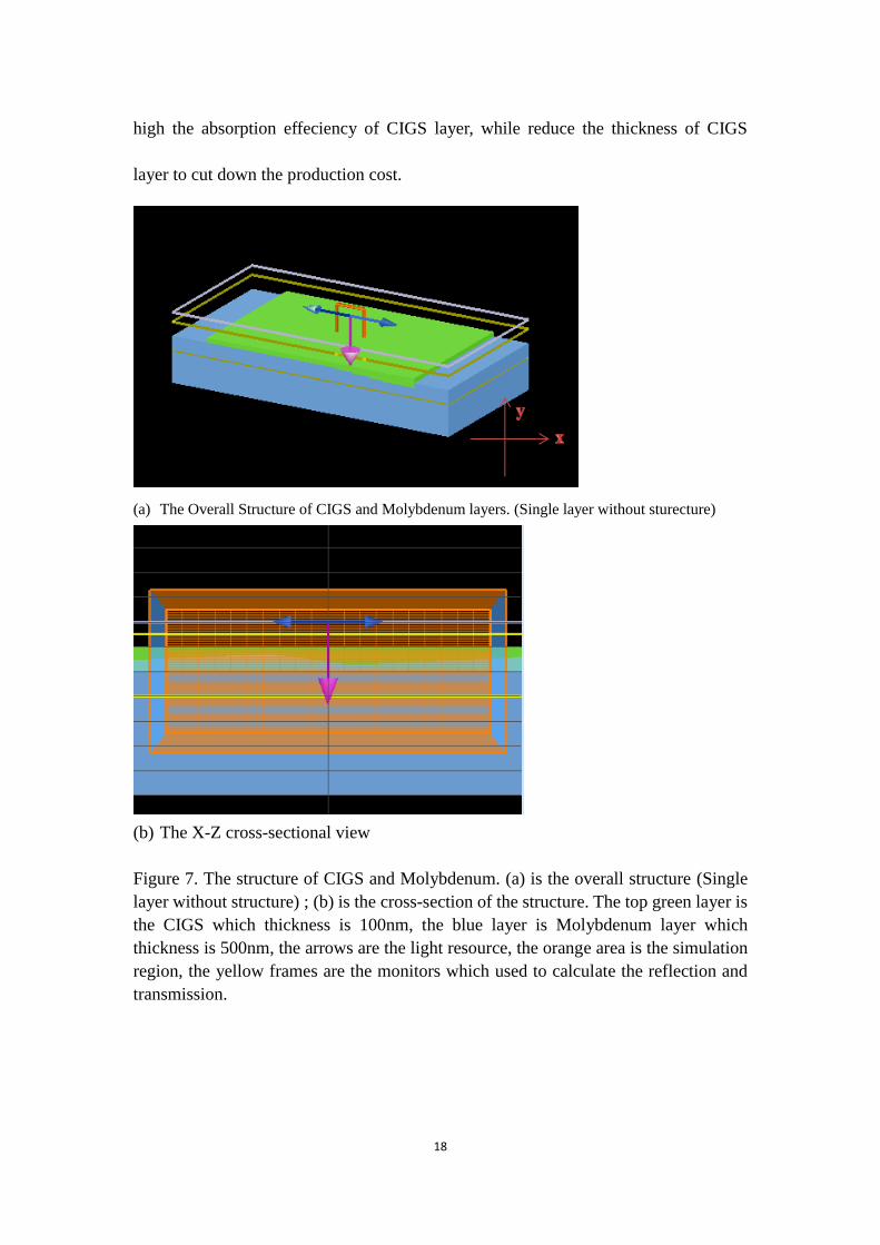
18
high the absorption effeciency of CIGS layer, while reduce the thickness of CIGS
layer to cut down the production cost.
(a) The Overall Structure of CIGS and Molybdenum layers. (Single layer without sturecture)
(b) The X-Z cross-sectional view
Figure 7. The structure of CIGS and Molybdenum. (a) is the overall structure (Single
layer without structure) ; (b) is the cross-section of the structure. The top green layer is
the CIGS which thickness is 100nm, the blue layer is Molybdenum layer which
thickness is 500nm, the arrows are the light resource, the orange area is the simulation
region, the yellow frames are the monitors which used to calculate the reflection and
transmission.

19
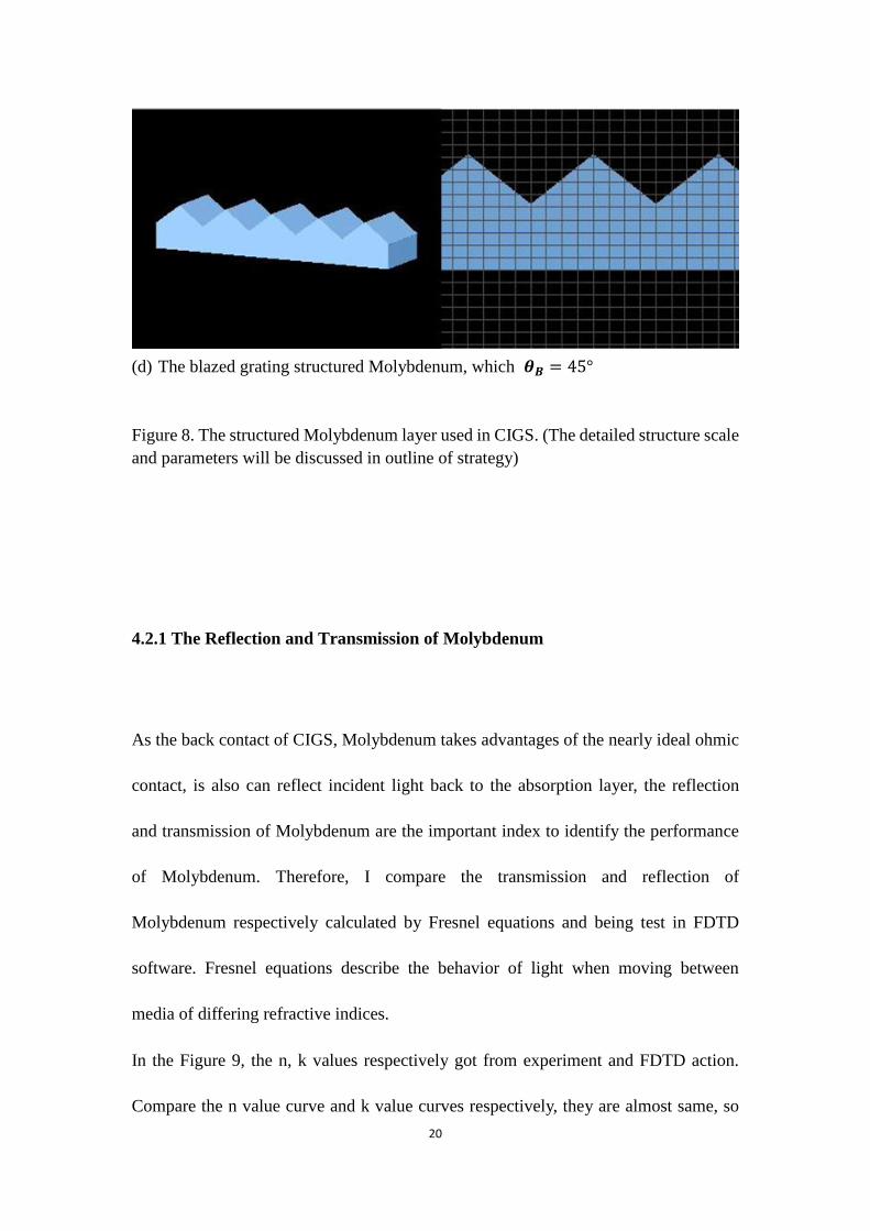
(a) The etching sphere structured Molybdenum.
(b) The hemisphere structured Molybdenum
(c) The blazed grating structured Molybdenum, which 𝜽𝑩 = 30°
20
(d) The blazed grating structured Molybdenum, which 𝜽𝑩 = 45°
Figure 8. The structured Molybdenum layer used in CIGS. (The detailed structure scale
and parameters will be discussed in outline of strategy)
4.2.1 The Reflection and Transmission of Molybdenum
As the back contact of CIGS, Molybdenum takes advantages of the nearly ideal ohmic
contact, is also can reflect incident light back to the absorption layer, the reflection
and transmission of Molybdenum are the important index to identify the performance
of Molybdenum. Therefore, I compare the transmission and reflection of
Molybdenum respectively calculated by Fresnel equations and being test in FDTD
software. Fresnel equations describe the behavior of light when moving between
media of differing refractive indices.
In the Figure 9, the n, k values respectively got from experiment and FDTD action.
Compare the n value curve and k value curves respectively, they are almost same, so
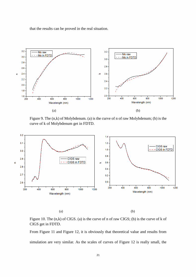
21
that the results can be proved in the real situation.
(a) (b)
Figure 9. The (n,k) of Molybdenum. (a) is the curve of n of raw Molybdenum; (b) is the
curve of k of Molybdenum get in FDTD.
(a) (b)
Figure 10. The (n,k) of CIGS. (a) is the curve of n of raw CIGS; (b) is the curve of k of
CIGS get in FDTD.
From Figure 11 and Figure 12, it is obviously that theoretical value and results from
simulation are very similar. As the scales of curves of Figure 12 is really small, the
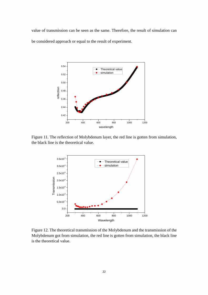
22
value of transmission can be seen as the same. Therefore, the result of simulation can
be considered approach or equal to the result of experiment.
200 400 600 800 1000 1200
0.42
0.44
0.46
0.48
0.50
0.52
0.54
re
fle
ctt
ion
wavelength
Theoretical value
simulation
Figure 11. The reflection of Molybdenum layer, the red line is gotten from simulation,
the black line is the theoretical value.
200 400 600 800 1000 1200
0.0
5.0x10⁻⁷
1.0x10⁻⁶
1.5x10⁻⁶
2.0x10⁻⁶
2.5x10⁻⁶
3.0x10⁻⁶
3.5x10⁻⁶
Tra
nsm
issio
n
Wavelength
Theoretical value
simulation
Figure 12. The theoretical transmission of the Molybdenum and the transmission of the
Molybdenum got from simulation, the red line is gotten from simulation, the black line
is the theoretical value.
23
4.2.2 The surface plasmon resonance of Molybdenum
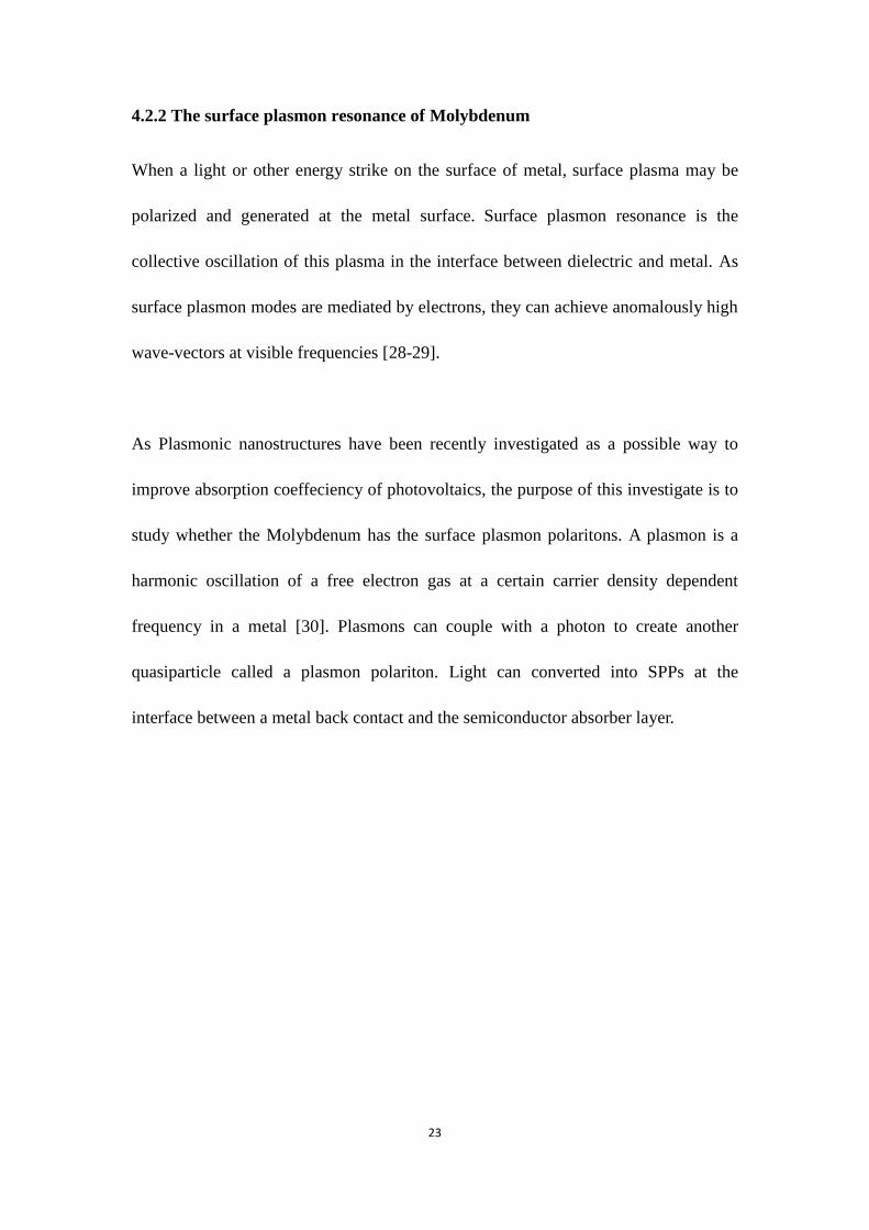
When a light or other energy strike on the surface of metal, surface plasma may be
polarized and generated at the metal surface. Surface plasmon resonance is the
collective oscillation of this plasma in the interface between dielectric and metal. As
surface plasmon modes are mediated by electrons, they can achieve anomalously high
wave-vectors at visible frequencies [28-29].
As Plasmonic nanostructures have been recently investigated as a possible way to
improve absorption coeffeciency of photovoltaics, the purpose of this investigate is to
study whether the Molybdenum has the surface plasmon polaritons. A plasmon is a
harmonic oscillation of a free electron gas at a certain carrier density dependent
frequency in a metal [30]. Plasmons can couple with a photon to create another
quasiparticle called a plasmon polariton. Light can converted into SPPs at the
interface between a metal back contact and the semiconductor absorber layer.

24
4.3 The outline of the Strategy
1) ZnO/CdSe nanowire array structure
The involved variable: the thickness (𝝁m), volume fraction (AVF). In this test, there
are three groups depend on the thickness of ZnO/CdSe nanowire, 10 𝝁m, 16 𝝁m,
24 𝝁m.
Thickness of ZnO/CdSe nanowire (𝑛m) Corresponds to Volume Fraction (AVF)
10 0.05, 0.10, 0.15, 0.20, 0.25, 0.30, 0.45,
16 0.05, 0.10, 0.15, 0.20, 0.25, 0.30,
24 0.05, 0.10, 0.15, 0.20, 0.25,
Table 2. The parameters of ZnO/CdSe nanowire arrays
. 2) Molybdenum use in Solar Cell
The thickness of Molybdenum layer is constant is 500nm, the purpose of change the
structures of surface connected to the absorber is to investigate whether the reflection
enhanced with structured Molybdenum.
The thickness of Molybdenum is relatively large, so that the thickness of structure
should control in 5nm to 20nm, the range can be achieved in the experiment.
(a) The Etching sphere structured Molybdenum
The structure has shown previously. Table 3 shows the paramaters of
Molybdenum structure
Diameter of Etching ball
(nm)
50 100 150 200
Wavelength of Source (nm) 300--1100
Thickness of Mo Layer (nm) 500
Table 3. The parameters of Etching sphere structured Molybdenum
25
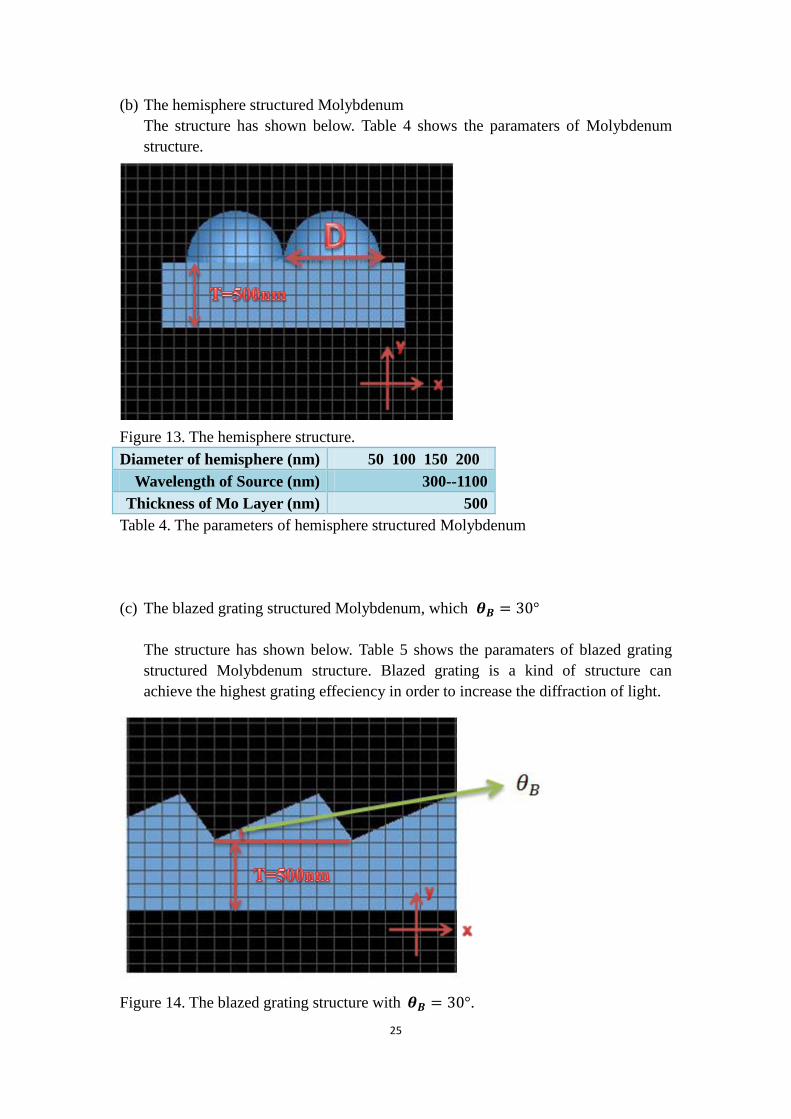
(b) The hemisphere structured Molybdenum
The structure has shown below. Table 4 shows the paramaters of Molybdenum
structure.
Figure 13. The hemisphere structure.
Diameter of hemisphere (nm) 50 100 150 200
Wavelength of Source (nm) 300--1100
Thickness of Mo Layer (nm) 500
Table 4. The parameters of hemisphere structured Molybdenum
(c) The blazed grating structured Molybdenum, which 𝜽𝑩 = 30°
The structure has shown below. Table 5 shows the paramaters of blazed grating
structured Molybdenum structure. Blazed grating is a kind of structure can
achieve the highest grating effeciency in order to increase the diffraction of light.
Figure 14. The blazed grating structure with 𝜽𝑩 = 30°.

26
The grating equation:
where:
= line spacing,
= incidence angle,
= diffraction angle,
= diffraction order,
= wavelength of incident light.
Figure 15. Diffraction at a blazed grating
If the kind of blazed grating is the Littrow configuration, which diffraction angle
and incidence angle are identical. The diffracted beam is back-reflected into the
direction of the incident beam. Hence, in Littrow configuration
The equation becomes: [31]
According to the equations, the parameters of blazed grating structured
Molybdenum shown in the Table. Through control the length d to change the
thickness of structure.
Table 5. The parameters of blazed grating structured Molybdenum, which 𝜽𝑩 = 30°
The length d (nm) 50 80 100 150
Wavelength of Source (nm) 300--1100
Thickness of Mo Layer (nm) 500
𝜽𝑩 30

27
(d) The blazed grating structured Molybdenum, which 𝜽𝑩 = 45°
The structure has shown below. Table shows the paramaters of blazed grating
structured Molybdenum structure.
Figure 16. The blazed grating structure with 𝜽𝑩 = 45°
The length d (nm) 30 50 80 100
Wavelength of Source (nm) 300--1100
Thickness of Mo Layer (nm) 500
𝜽𝑩 45
Table 6. The parameters of blazed grating structured Molybdenum, which 𝜽𝑩 = 45°
28
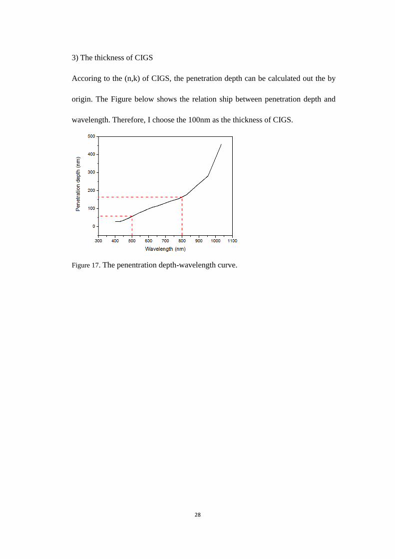
3) The thickness of CIGS
Accoring to the (n,k) of CIGS, the penetration depth can be calculated out the by
origin. The Figure below shows the relation ship between penetration depth and
wavelength. Therefore, I choose the 100nm as the thickness of CIGS.
Figure 17. The penentration depth-wavelength curve.
29
Chapter 5 Result and Discussion
5.1 The Optimal Geometry of ZnO/CdSe Nanowire array
(a) (b)
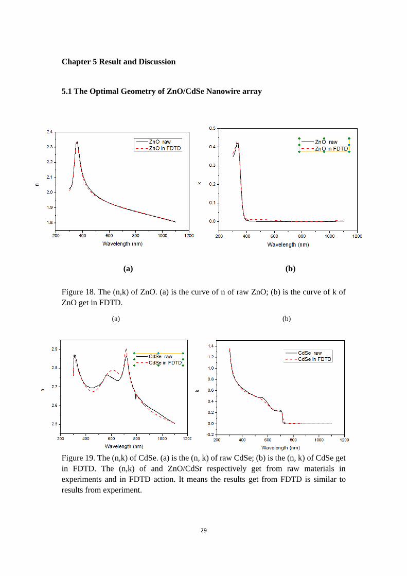
Figure 18. The (n,k) of ZnO. (a) is the curve of n of raw ZnO; (b) is the curve of k of
ZnO get in FDTD.
(a) (b)
Figure 19. The (n,k) of CdSe. (a) is the (n, k) of raw CdSe; (b) is the (n, k) of CdSe get
in FDTD. The (n,k) of and ZnO/CdSr respectively get from raw materials in
experiments and in FDTD action. It means the results get from FDTD is similar to
results from experiment.
30
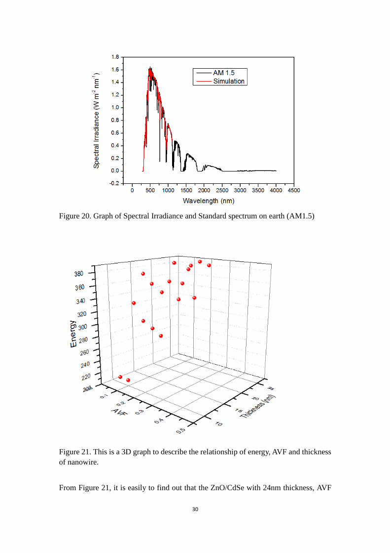
Figure 20. Graph of Spectral Irradiance and Standard spectrum on earth (AM1.5)
Figure 21. This is a 3D graph to describe the relationship of energy, AVF and thickness
of nanowire.
From Figure 21, it is easily to find out that the ZnO/CdSe with 24nm thickness, AVF
31
0.20 has the highest the energy of absorption. Therefore, the optimal geometry
ZnO/CdSe nanowire array is the AVF 0.20, thickness is 24nm one.
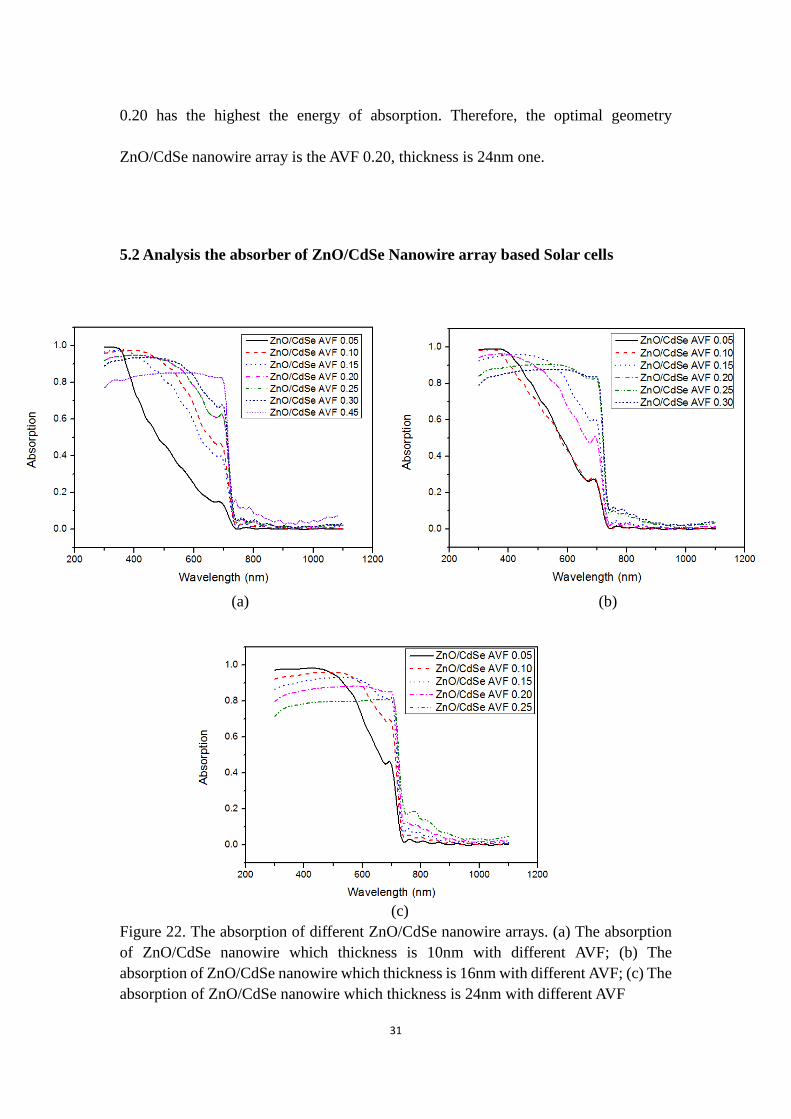
5.2 Analysis the absorber of ZnO/CdSe Nanowire array based Solar cells
(a) (b)
(c)
Figure 22. The absorption of different ZnO/CdSe nanowire arrays. (a) The absorption
of ZnO/CdSe nanowire which thickness is 10nm with different AVF; (b) The
absorption of ZnO/CdSe nanowire which thickness is 16nm with different AVF; (c) The
absorption of ZnO/CdSe nanowire which thickness is 24nm with different AVF
32
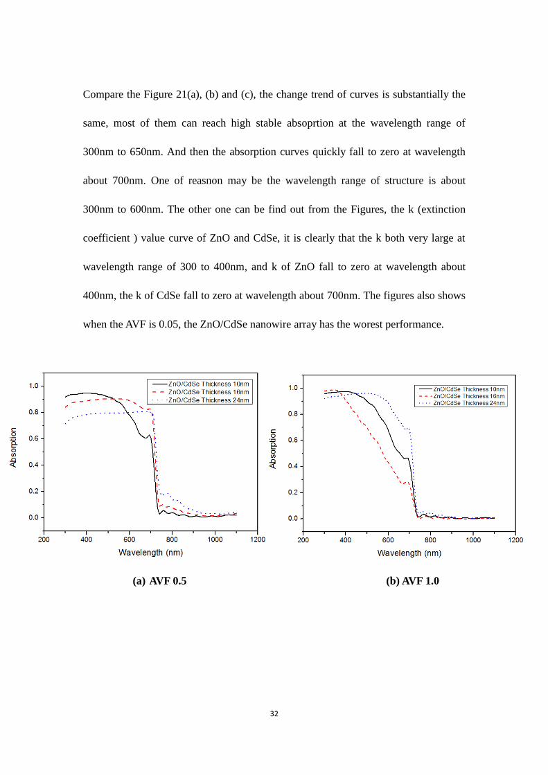
Compare the Figure 21(a), (b) and (c), the change trend of curves is substantially the
same, most of them can reach high stable absoprtion at the wavelength range of
300nm to 650nm. And then the absorption curves quickly fall to zero at wavelength
about 700nm. One of reasnon may be the wavelength range of structure is about
300nm to 600nm. The other one can be find out from the Figures, the k (extinction
coefficient ) value curve of ZnO and CdSe, it is clearly that the k both very large at
wavelength range of 300 to 400nm, and k of ZnO fall to zero at wavelength about
400nm, the k of CdSe fall to zero at wavelength about 700nm. The figures also shows
when the AVF is 0.05, the ZnO/CdSe nanowire array has the worest performance.
(a) AVF 0.5 (b) AVF 1.0
33
(c) AVF 1.5 (d) AVF 2.0
(e) AVF 2.5
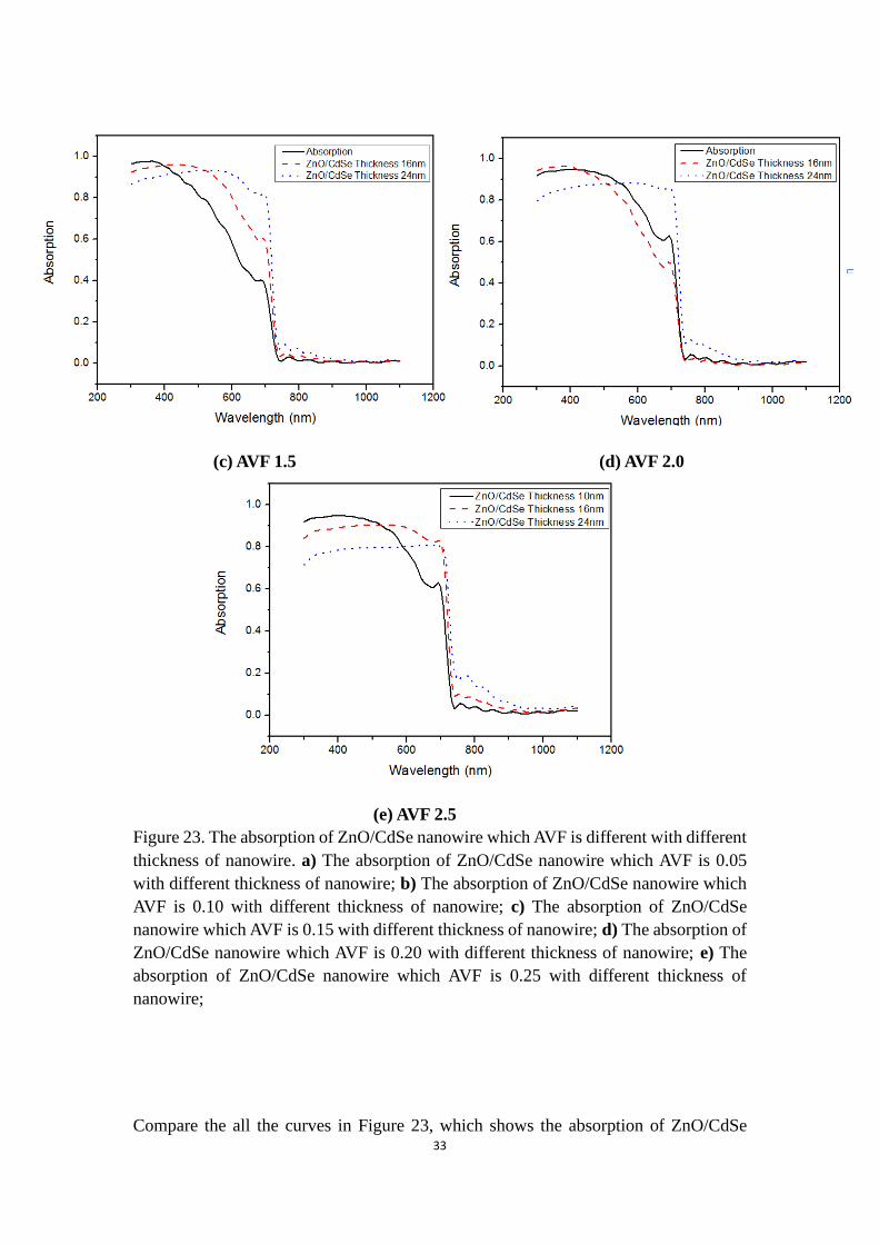
Figure 23. The absorption of ZnO/CdSe nanowire which AVF is different with different
thickness of nanowire. a) The absorption of ZnO/CdSe nanowire which AVF is 0.05
with different thickness of nanowire; b) The absorption of ZnO/CdSe nanowire which
AVF is 0.10 with different thickness of nanowire; c) The absorption of ZnO/CdSe
nanowire which AVF is 0.15 with different thickness of nanowire; d) The absorption of
ZnO/CdSe nanowire which AVF is 0.20 with different thickness of nanowire; e) The
absorption of ZnO/CdSe nanowire which AVF is 0.25 with different thickness of
nanowire;
Compare the all the curves in Figure 23, which shows the absorption of ZnO/CdSe
34
nanowire which AVF is 0.05, 0.10, 0.15, 0.20, 0.25 with different hexagonal prism
thickness, at the range of visible light wavelength, the ZnO/CdSe nanowire which
thickness is 24nm has relatively best performance of absorption. When the volume
fraction reaches to 0.25, the thinner layer has the better performance of absorption.
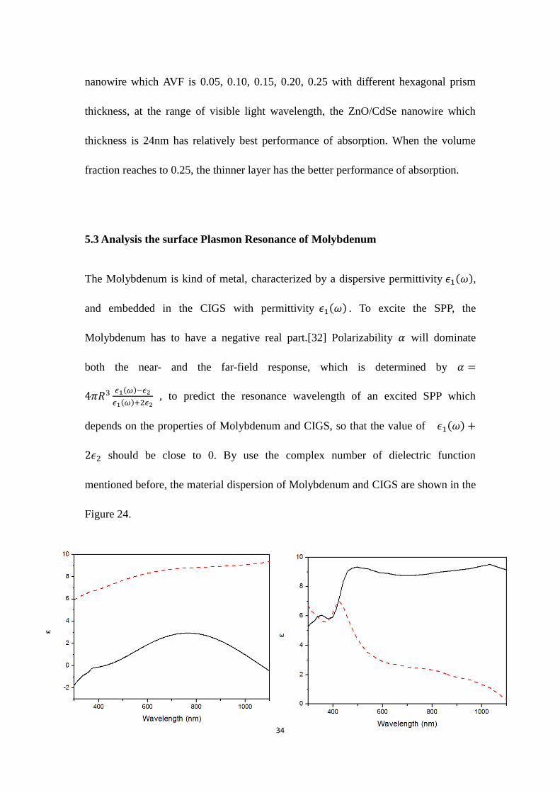
5.3 Analysis the surface Plasmon Resonance of Molybdenum
The Molybdenum is kind of metal, characterized by a dispersive permittivity 𝜖1(𝜔),
and embedded in the CIGS with permittivity 𝜖1(𝜔) . To excite the SPP, the
Molybdenum has to have a negative real part.[32] Polarizability 𝛼 will dominate
both the near- and the far-field response, which is determined by 𝛼 =
4𝜋𝑅3 𝜖1(𝜔)−𝜖2
𝜖1(𝜔)+2𝜖2 , to predict the resonance wavelength of an excited SPP which
depends on the properties of Molybdenum and CIGS, so that the value of 𝜖1(𝜔) +
2𝜖2 should be close to 0. By use the complex number of dielectric function
mentioned before, the material dispersion of Molybdenum and CIGS are shown in the
Figure 24.

35
(a) Molybdenum (b) CIGS
Figure 24. The permittivity of (a) Molybdenum and (b) CIGS.
From the Figure 23, the required metallic properties occur for Molybdeunum at
wavelengths below 400nm. Therefore, 𝜖1(𝜔) will be over zero at the most visible
light wavelength range, and 𝜖2 related to CIGS is always over zero, so that the
𝜖1(𝜔) + 2𝜖2 could not close to zero, it is means that the Molybdenum could not
excite the SPP.
36
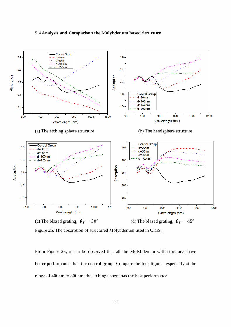
5.4 Analysis and Comparison the Molybdenum based Structure
(a) The etching sphere structure (b) The hemisphere structure
(c) The blazed grating, 𝜽𝑩 = 30° (d) The blazed grating, 𝜽𝑩 = 45°
Figure 25. The absorption of structured Molybdenum used in CIGS.
From Figure 25, it can be observed that all the Molybdenum with structures have
better performance than the control group. Compare the four figures, especially at the
range of 400nm to 800nm, the etching sphere has the best performance.
37
Chapter 6 Conclusions
Solar cells or photovoltaics as a kind of device that can convert the sunlight into
electricity have been extensively studied and widely used. In order to investigate the
ways to improve the absorption of solar cells, the research is divided into two parts. In
the part A, the structure of ZnO/CdSe nanowire is designed as hexagonal prism. After
analysis the results of the absorption of different sized structure, it can be seen that the
structures with volume fraction is 0.20 and thickness is 24nm have the better
performance on absoption. And absorption coffeciency of ZnO/CdSe nanowire array
are very high, especially at the range of visible light wavelength.
In part B, the Molybdenum is used as a metal back contact in CIGS devices. The
original purpose is to investigate the Surface Plasmon Polaritons (SPPs) at the
interface between the Molybdenum and absorb layer. From the results and analysis,
there is no indication that SPPs happened in visible light wavelength on the
metal/semiconductor interface. However, the structure of Molybdenum also can
increase the absorption of the overall structure, so that can improve the performance
of solar cell.

38
References
[1] E.T. Yu and J. van de Lagemaat, Photon management for photovoltaics. MRS BULLETIN .
VOLUME 36, (2011) [2] Arul Lenus Roy VELLAISAMY, Chapter 6 of Energy Materials for Solar and Fuel Cell. [3] Hadiseh Alaeian, Ashwin C Atre and Jennifer A Dionne, Optimized light absorption in Si wire
array solar cells J. Opt. 14 (2012) 024006 (6pp) [4] I. Repins, M.A. Contreras, B. Egaas, C. DeHart, J. Scharf, C.L. Perkins, B. To, and R. Noufi, Prog.
Photovolt. Res. Appl. 16,235 (2008). [5] Fu-qiang HUANG, Chong-yin YANG, Dong-yun WAN, Advanced solar materials for thin-film
photovoltaic cells. Front. Phys., 2011, 6(2): 177–196. DOI 10.1007/s11467-011-0173-4 [6] Umran S. Inan and Robert A. Marshal .Numerical Electromagnetics: The FDTD Method. ISBN
978-0-521-19069-5 Hardback (2011) [7] Lumerical Solutions, Inc. FDTD_getting_started [8] Jan Kupec and BerndWitzigmann, Computational electromagnetics for nanowire solar cells. J
Comput Electron (2012) 11:153–165 [9] Stephen D. Gedeny. Introduction to the Finite-Difference Tme-Domain (FDTD) Method for
Electromagnetics [10] The Solar and Wind Expo. Stanford researchers develop new technology for cheaper, more
efficient solar cells, http://thesolarandwindexpo.blogspot.hk/2011/02/stanford-researchers-develop-new.html
[11] Plexcore PV for Printed Solar Power. [12] Jenny Nelson, The Physics of Solar Cells, 2003 [13] Hadiseh Alaeian,, Ashwin C Atre and Jennifer A Dionne,Optimized light absorption in Si
wire array solar cells, JOURNAL OF OPTICS, J. Opt. 14 (2012) 024006 (6pp).
[14] F. Kadırgan, Electrochemical Nano-Coating Processes in Solar Energy Systems. Volume 2006,
Article ID 84891, Pages 1–5. DOI 10.1155/IJP/2006/84891.
[15] Henne van Heeren, Fabrication for Nanotechnology [16] Harry A. Atwater and Albert Polman. Plasmonics for improved photovoltaic devices Nature
Mater. Nature materala Vol 9 (2010). DOI: 10.1038/NMAT2629. [17] Shrestha Basu Mallick et. Coherent light trapping in thin-film photovoltaics. MRS BULLETIN
VOLUME 36 (2011). DOI: 10.1557/mrs.2011.113 [18] Erik Garnett and Peidong Yang, Light Trapping in Silicon Nanowire Solar Cells. Nano Lett.
1082–1087 (2010). DOI: 10.1021/nl100161z [19] Lumerical Solutions, Inc. FDTD Solutions Introductory Training
[20] FDTD Solution Knowledge Base. http://docs.lumerical.com/en/fdtd/ref_fdtd_physics_maxwell.html
[21] Yee, K.: IEEE Trans. Antennas Propag. 14(3), 302 (1966) [22] Yu, W., Mittra, R., Yang, X., Liu, Y., Rao, Q., Muto, A.: IEEE Microw. Mag. 11(4), 43 (2010) [23] OptiFDTD: Technical Background and Tutorials; Finite Difference Time Domain
Photonics Simulation Software, Optiwave, 2009 [24] Steven G. Johnson, 22 August 2006 (UTC) See als [25] J.A. WOOLLAM CO. INC. Dielectric Function
[26] Yiwen Tang, Xiaoyan Hu. CdSe nanocrystal sensitized ZnO core-shell nanorod array films:
Preparation and photovoltaic properties. Electrochimica Acta, Vo 54, Issue 10,pages
2742-2747(2009).
[27] Marika Edoff, Sebastian Schleussner. Technological and economical aspects on the influence of reduced Cu(In,Ga)Se2 thickness and Ga grading for co-evaporated Cu(In,Ga)Se2
modules. Thin Solid Films 519 (2011) 7530–7533.

39
[28] A. Graff, D. Wagner, H. Ditlbacher and U. Kreibig, European Physical Journal D, vol. 34,
p.263 (2005). [29] Kittel, C.: "Introduction to Solid State Physics", 8th edition, Wiley 2005 [30] Ana Belén Cristóbal López,Antonio Martí Vega,Antonio Luque López, Next Generation of
Photovoltaics: New Concepts.
[31] Wikipedia Contributors, http://en.wikipedia.org/wiki/Blazed_grating
[32] Carsten Rockstuhl, Stephan Fahr, and Falk Lederer. Chapter 5, Surface Plasmon Polaritons in
Metallic Nanostructures: Fundamentals and Their Application to Thin-Film Solar Cells
Related Documents