PerkinElmer proprietary information P AS (Rev 1.2 / 95510862 / 2005-12-15) Specifications are subject to change without notice. XRD 1620 AN X-Ray Detector Reference Manual

Welcome message from author
This document is posted to help you gain knowledge. Please leave a comment to let me know what you think about it! Share it to your friends and learn new things together.
Transcript

PerkinElmer proprietary information P AS (Rev 1.2 / 95510862 / 2005-12-15) Specifications are subject to change without notice.
XRD 1620 AN X-Ray Detector
Reference Manual

PerkinElmer proprietary information Page ii P AS (Rev 1.2 / 95510862 / 2005-12-15) Specifications are subject to change without notice
HIS-Reference-Book Proprietary Information
XRD 1620 AN Reference Manual
FOR YOUR SAFETY
Warning Read the manual and all accompanying papers carefully before operating the XRD 1620
system to avoid any damage and personal injury.
The system is intended for use by qualified personnel who are familiar with the operation of electrical equipment (considering safety precautions to avoid possible injuries)
The system should only be installed by qualified personnel who are familiar with the installation of electrical equipment (considering safety precautions to avoid possible injuries and damage to the system)
The X-Ray Detector is intended to operate from a power source that will not apply more than 240 Volts rms between the supply conductors or between either supply conductor and ground. Other system components have to be grounded through the protection earth conductors in the power cords:
• Computer with frame grabber
• Monitor
The required potential equalization has to be managed through the labeled connectors at the and the XRD-EP power supply.
To avoid electrical shock, plug the power cords into a properly wired receptacle before performing all other connections. For best performance avoid receptacles which are not properly grounded
Exercise extreme care to select a low noise, ripple free ground connection for the whole system. Ground terminals of wall receptacles are not suitable to ground the detector housing due to high noise and ripple input into the system.
If the protective-ground connection is lost, all accessible conductive parts can render an electric shock, including the parts which appear to be isolated.
Use only the original power cords. Inspect power cords and connectors regularly. Cord and connector repairs should only be serviced by qualified personnel.
Be sure to operate the X-Ray Detector with the specified power supply. Use of an incorrect voltage will cause system failure and create a hazard.
If any abnormal phenomena are evident such as smoke, strange sounds or fumes, unplug the Power Supply and contact your dealer, distributor or PerkinElmer Optoelectronics subsidiaries (page 32) immediately. Further use may be dangerous.
Removing the housing of the X-Ray Detector or of the Power-Supply may cause electrical shock and/or irreparable damage of highly sensitive components.
Do not place any objects in the X-Ray Detector or in the power supply. In case of an accident, unplug the power supply immediately and contact your dealer, distributor or PerkinElmer Optoelectronics subsidiaries (page 32). Using the X-Ray Detector or the power supply any longer may cause fire, electrical shock or other damage.
Install the X-Ray Detector on a flat, stable surface. The X-Ray Detector may cause an injury if it falls or is dropped.
Do not place the X-Ray Detector or other components on or near other devices.
Do not use the X-Ray Detector or the power supply near water or other liquids Water contact to the X-Ray Detector the power supply and may cause fire, electrical shock as well as damage the device(s).

PerkinElmer proprietary information Page iii P AS (Rev 1.2 / 95510862 / 2005-12-15) Specifications are subject to change without notice
HIS-Reference-Book Proprietary Information
XRD 1620 AN Reference Manual
Caution Do not operate the system in or around flammable gases or liquids.
Temperature changes Fire, electric shock, and/or damage may occur if the X-Ray Detector is used in dusty, humid, or smoky areas or areas subjected to sudden temperature changes.
Environmental Conditions Environmental conditions that are not in compliance with Section 3 of this manual may reduce the lifetime and/or irreparably damage the X-Ray Detector.
Disconnect the cables prior to moving the XRD 1620. Prior to moving the X-Ray Detector, unplug all cables and turn off the power supply.. Disconnect the cables by use in the plug and not the cable itself as stressing the cable may cause fire or electrical shock. It is recommended that two people are used to move the XRD 1620.
Do not touch the plug with wet hands Pulling or inserting the plug with wet hands may cause electrical shock.
Do not touch the XRD 1620 or the power supply XRD-EP and the patient at the same time.
Do not use more than 25 Vac and/or 60Vdc at SIP/SOP.
EMC Safety Medical Devices are in need of special precautions concerning EMC and should be installed
and operated as written in the accompanying documentation.
High electro magnetic fields near the X-Ray Detector or the data cables may result in erroneous readings.
Mobile RF-communication devices near the X-Ray Detector or the data cables may result in erroneous readings.
Only original components should be used, and no modifications and/or alterations to the product or any portion thereof should be performed without obtaining the prior written authorization of PerkinElmer.
ESD Safety Shut down the power supply before connecting or disconnecting any cables.
Only original components should be used, and no modifications and/or alterations to the product or any portion thereof should be performed without obtaining the prior written authorization of PerkinElmer.
The system must be grounded through the grounding conductors of the power cords and in addition a protective potential equalization is required for the X-Ray Detector XRD 1620, and the power supply XRD-EP.
Proper Electrostatic Discharge protection must be used prior to handling electrical connections to the X-Ray Detector

PerkinElmer proprietary information Page iv P AS (Rev 1.2 / 95510862 / 2005-12-15) Specifications are subject to change without notice
HIS-Reference-Book Proprietary Information
XRD 1620 AN Reference Manual
Cleaning Only cloth lightly moistened with a mild detergent solvent and afterwards a soft dry cloth
should be used.
For safety reasons, turn off and unplug the power supply and unplug before cleaning.
Never use any of the following strong solvents as damage to the X-Ray Detector and accessories may occur.
o Thinner
o Benzine
o Abrasive cleaner
o Wax
o Acid or Alkaline solvent
o Spray-type cleaner

PerkinElmer proprietary information Page v P AS (Rev 1.2 / 95510862 / 2005-12-15) Specifications are subject to change without notice
HIS-Reference-Book Proprietary Information
XRD 1620 AN Reference Manual
Table of Contents
1 SCOPE ............................................................................................................................................................. 1
2 REGULATORY REQUIREMENTS....................................................................................................................... 1
3 ENVIRONMENTAL CONSIDERATIONS.............................................................................................................. 1
4 DESCRIPTION OF THE XRD 1620 ..................................................................................................................... 2 4.1 PRINCIPLE OF THE XRD 1620 ........................................................................................................................ 2 4.2 ELECTRONIC CONTROL AND READOUT .............................................................................................................. 3 4.3 STRUCTURE OF THE XRD 1620 AN................................................................................................................. 3 4.4 DETECTOR OVERVIEW .................................................................................................................................. 4
5 XRD 1620 SPECIFICATION ............................................................................................................................... 5 5.1 TECHNICAL DATA OF THE XRD 1620 ................................................................................................................ 5
5.1.1 Mechanical specification ..................................................................................................................... 5 5.1.2 Readout Specification ......................................................................................................................... 7 5.1.3 Connectors of the XRD 1620 AN.......................................................................................................... 8 5.1.4 Accessories ....................................................................................................................................... 9 5.1.5 Detector Modes and Timings ............................................................................................................... 9 5.1.6 Information ...................................................................................................................................... 10
5.2 PIXEL DEFECT SPECIFICATION ...................................................................................................................... 10 5.2.1 General Definitions ........................................................................................................................... 10 5.2.2 Definition of Cluster .......................................................................................................................... 10 5.2.3 Definition of Panel Regions ............................................................................................................... 10 5.2.4 Definition of Bad Pixel Measurement .................................................................................................. 10 5.2.5 Number of Pixel Defect ..................................................................................................................... 12
5.3 POWER SUPPLY XRD-EP ............................................................................................................................ 14 5.4 FRAME GRABBER BOARD............................................................................................................................. 16
5.4.1 The XRD-FG PCI interface board...................................................................................................... 16 5.4.2 Connectors of the Frame Grabber...................................................................................................... 17 5.4.3 Installation of the Frame Grabber ....................................................................................................... 17
5.5 X-RAY IMAGING SOFTWARE LIBRARY (XISL) ................................................................................................... 19 5.5.1 Description of file header................................................................................................................... 21 5.5.2 Interrupt sources .............................................................................................................................. 22 5.5.3 Sorting schemes overview................................................................................................................. 23
6 OPERATIONAL FUNCTIONS ........................................................................................................................... 24 6.1 GETTING STARTED - THE FIRST IMAGE............................................................................................................ 24
6.1.1 Introduction...................................................................................................................................... 24 6.1.2 General considerations ..................................................................................................................... 24 6.1.3 Connection of the XRD 1620 ............................................................................................................. 24 6.1.4 The first image ................................................................................................................................. 25
6.2 HOW TO PERFORM CORRECTIONS.................................................................................................................. 25 6.2.1 Use of the Offset Correction .............................................................................................................. 26 6.2.2 Use of the Gain/Offset Correction ...................................................................................................... 27 6.2.3 Use of Multiple Gain Correction ......................................................................................................... 27 6.2.4 Use and generation of the Pixel Correction ......................................................................................... 28 6.2.5 Correct previously acquired images.................................................................................................... 28
6.3 HOW TO RUN THE DETECTOR ...................................................................................................................... 28 6.3.1 Free Running ................................................................................................................................... 28 6.3.2 Internal Trigger ................................................................................................................................ 29 6.3.3 External Trigger ............................................................................................................................... 29
PerkinElmer proprietary information Page vi P AS (Rev 1.2 / 95510862 / 2005-12-15) Specifications are subject to change without notice
HIS-Reference-Book Proprietary Information
XRD 1620 AN Reference Manual
6.3.4 Internal Trigger ................................................................................................................................ 30 6.3.5 How to use the internal trigger mode .................................................................................................. 30
6.4 HOW TO USE THE DETECTOR GAIN SETTING ..................................................................................................... 31 6.5 MAINTENANCE ........................................................................................................................................... 31 6.6 DISPOSAL ................................................................................................................................................. 31
7 AFTER-SALES SERVICE FOR PERKINELMER PRODUCTS ............................................................................. 32
8 GUIDANCE AND MANUFACTURER’S DECLARATION ..................................................................................... 33 List of FiguresFig. 1 Principle electronic arrangement of XRD 1620............................................................................. 2 Fig. 2 Structure of the XRD 1620 AN............................................................................................................................ 3 Fig. 3 Detector Overview............................................................................................................................................. 4 Fig. 4 Mechanical drawing of the XRD 1620 A............................................................................................................... 6 Fig. 5 Drawing of the power supply connector (front view) ........................................ Fehler! Textmarke nicht definiert. Fig. 6 Drawing of the connector for triggering (front view) ............................................................................................... 8 Fig. 7 Image of the Power Supply XRD-EP ................................................................................................................. 14 Fig. 8 Image of the XRD-FG Frame Grabber.............................................................................................................. 17 Fig. 9 Interrupt sources at a) sequence (4 frames) and b) continuous acquisition mode................................................... 22 Fig. 10 Sorting scheme of the XRD 1620 .................................................................................................................... 23 Fig. 11 Connections of the XRD 1620 ........................................................................................................................ 24 Fig. 12 General timing diagram in continuous mode..................................................................................................... 29 Fig. 13 General timing diagram in triggered mode ....................................................................................................... 29
List of Tables Table 1 Regulatory Requirements................................................................................................................................ 1 Table 2 Environnemental Considerations...................................................................................................................... 1 Table 3 Detector Overview .......................................................................................................................................... 4 Table 4 Mechanical specification ................................................................................................................................. 5 Table 5 Readout Specification ..................................................................................................................................... 7 Table 6 PIN assignment of Trigger signal ..................................................................................................................... 8 Table 7 Accessories for the XRD 1620 ......................................................................................................................... 9 Table 8 Status Lights of the XRD-EP.......................................................................................................................... 14 Table 9 Electrical and Mechanical Specification of the XRD-EP .................................................................................... 15 Table 10 PIN assignment of power supply XRD-EP ..................................................................................................... 15 Table 11 Environmental Considerations for the Power Supplies.................................................................................... 15 Table 12 Frame Grabber Specification ....................................................................................................................... 16 Table 13 Environmental Considerations for the Frame Grabber .................................................................................... 16 Table 14 List of XISL modules ................................................................................................................................... 20 Table 15 File header description ................................................................................................................................ 21 Table 16 Overview of the five Detector Gain Settings................................................................................................... 31 Table 17 Guidance and Manufacturer’s Declaration of Electromagnetic Emissions ......................................................... 33 Table 18 Guidance and Manufacturer’s Declaration of Electromagnetic Immunity ........................................................... 33 Table 19 Guidance and Manufacturer’s Declaration of Electromagnetic Immunity (Portable Equipment) ........................... 34 Table 20 Recommended Separation Distance between Portable and Mobile RF-Communication Equipment and the X-Ray Detector .................................................................................................................................................................. 35

PerkinElmer proprietary information Page 1 P AS (Rev 1.2 / 95510862 / 2005-12-15) Specifications are subject to change without notice
HIS-Reference-Book Proprietary Information
XRD 1620 AN Reference Manual
1 Scope This document describes design elements and respective interfaces. Where applicable mechanical, electronic, and software interfaces will be addressed
2 Regulatory Requirements The assembly of the X-Ray Detector XRD 1620 is designed to be compliant with the requirements detailed in the table below. All regulatory certificates are valid only if the original accessories as listed in Table 7 are used. All regulatory certificates are rendered invalid if any modifications and/or alterations to the Product are made, or any portion thereof, without obtaining the prior written authorization of PerkinElmer. Standard Description INTERNATIONAL IEC 60950 Safety of information technology equipment including electrical business equipment
and associated equipment, with a rated voltage not exceeding 600V. UL 60601-1 General Requirements for Safety and Electromagnetic Compatibility for Medical
Electrical Equipment (US) EUROPEAN EN 60950 A497 Safety of information technology equipment including electrical business equipment
and associated equipment, with a rated voltage not exceeding 600V EN 60601-1 General Requirements for Safety and Electromagnetic Compatibility for Medical
Electrical Equipment EN 60601-1-2:2001 Medical electrical equipment, Part 1-2: General requirements for safety - Collateral
standard: Electromagnetic compatibility
Table 1 Regulatory Requirements
3 Environmental Considerations Environments outside the specification reduce the lifetime and may irreparably damage the Product.
Transportation / Storage*1 Operation
Ambient temperature 0° to +50°C 0° to +45°C (CsJ)*2 +15° to +35°C
Relative humidity*3 5% to 90% 10% to 80% (CsJ) 30% to 70%
Atmospheric pressure 700 to 1250 hPas 800 to 1250 hPas
Vibration 2g (10 Hz to 150 Hz) 0.5g (10Hz to 150Hz)
Shock 20g (duration 6-10ms) 2g (duration 11ms) Note: *1 In original transport container
*2 Temp. Gradient: max 4.5 K/hour *3 No condensation
Table 2 Environnemental Considerations

PerkinElmer proprietary information Page 2 P AS (Rev 1.2 / 95510862 / 2005-12-15) Specifications are subject to change without notice
HIS-Reference-Book Proprietary Information
XRD 1620 AN Reference Manual
4 Description of the XRD 1620
4.1 Principle of the XRD 1620 The detector XRD 1620 works as a complete X-Ray detector, the sensor and its electronics are housed in one package. In order to increase the durability of the device in MeV source applications , the electronics are placed on the perimeter of the active sensor, out of the direct path of the beam. No lead shielding is provided for the electronics, and thus the customer is required to block the radiation by lead shielding to avoid damage of the electronics, and to adjust the field of view (FOV) to the active area. Any portion of the housing outside of the Field of View has to be protected such that the overall applied dose does not harm the electronic components. The removable aluminum plate in the housing protects the sensor against mechanical impacts only and is not designed to shield the electronics from X-Rays. The PROM used for the FPGA downloading has an additional window and is placed on the front of the housing. The cover is designed to allow an exchange of the PROM. The flat panel sensor of the XRD 1620 is fabricated using thin film technology based on amorphous silicon technology. Electronically, the sensors are much like conventional photodiode arrays. Each pixel in the array consists of a light-sensing photodiode and a switching Thin Film Transistor (TFT) in the same electronic circuit. Amorphous silicon photodiodes are sensitive to visible light, with a response curve roughly comparable to human vision. The sensitivity of amorphous silicon photodiodes peaks in green wavelengths, well matched to scintillators such as CsI or Gd2O2S:Tb(commercially available as LANEX® scintillators). The response has the excellent linearity of a charge-integrating biased photodiode. These sensors are of special interest primarily for the size. The XRD 1620 sensor is based on a single panel. This means that no optical reduction is needed when recording large images, as from conventional X-ray cameras. The panel provides a very large improvement in the capture of optical photons from the scintillator when compared to a fiber optic taper or reducing lens.
Fig. 1 Principle electronic arrangement of XRD 1620
PerkinElmer proprietary information Page 3 P AS (Rev 1.2 / 95510862 / 2005-12-15) Specifications are subject to change without notice
HIS-Reference-Book Proprietary Information
XRD 1620 AN Reference Manual
The incident X-rays are converted by the scintillator material to visible light which generates electron hole pairs in the biased photodiode. The charge carriers are stored in the capacity of the photodiode. By pulsing the gates of a TFT line within the matrix, the charges of all columns are transferred in parallel to the signal outputs. All signals of the columns are amplified in custom readout multiplexers for further processing (see Fig. 1).
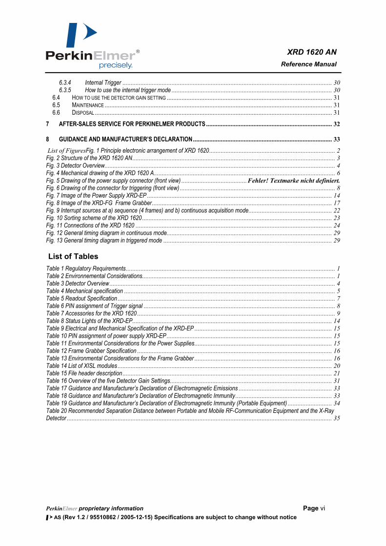
4.2 Electronic control and readout Charge amplifiers for readout of the sensor, and row drivers for addressing the rows are placed on chip on board (COB) modules contacting the pads at the edges of the sensor. The COBs for control and readout are connected to A/D conversion PCB boards. The analog part of the electronics is placed beside the sensor and includes sophisticated FPGA control of the detector. Numerous features are realized to minimize noise, as well as shaping and timing of the control pulses and isolation of digital and analog sections. The digital control is reprogrammable through a PROM to enable future upgrades or modifications.
4.3 Structure of the XRD 1620 AN
16” x 16” a-Si panel
COBBM
COBBM
COB BM
A/D A/D A/D
COBY
COBY
COBY
A
A
A COB Y
COB Y
A
A
COB Y A
COBBM
COBBM
COB BM
A/D A/D A/D
1stlevel
2nd levelelectronics
3rd level electronics
DigitalControl
Unit
PC
Power XRD-EP
Soft - ware
Interface BUS
TriggerUnit
Frame grabber
Housing
Trigger-Interface
XRD-FG
Fig. 2 Structure of the XRD 1620 AN

PerkinElmer proprietary information Page 4 P AS (Rev 1.2 / 95510862 / 2005-12-15) Specifications are subject to change without notice
HIS-Reference-Book Proprietary Information
XRD 1620 AN Reference Manual
4.4 Detector Overview
Fig. 3 Detector Overview
1 Potential Equalization 2 Ground Connector 3 Trigger Input (page 7) 4 Power Input (page 3) 5 XRD Interface Bus 6 Detector Mode and Frame Rate (page 9)
Green Free Running Yellow Trigger Mode
7 Power On and Detector Status
Green Power ON Orange Self Inspection
6 + 7 All Lights On during Self Inspection (Power-ON)
8 PROM Holder 9 Electronics (This Area needs to be shielded) 10 Active Area
Table 3 Detector Overview

PerkinElmer proprietary information Page 5 P AS (Rev 1.2 / 95510862 / 2005-12-15) Specifications are subject to change without notice
HIS-Reference-Book Proprietary Information
XRD 1620 AN Reference Manual
5 XRD 1620 Specification
5.1 Technical data of the XRD 1620
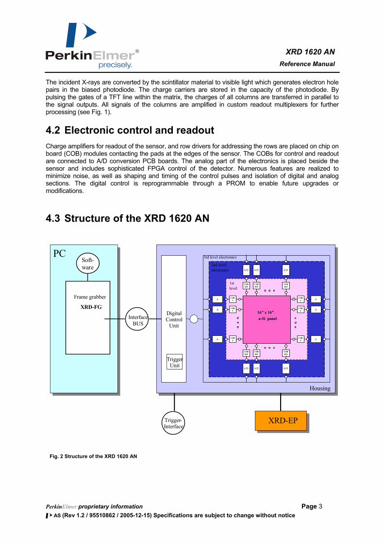
5.1.1 Mechanical specification
Size: 672 mm x 599 mm x 44 mm Weight: approximately 25 kg. Connectors: 50-PIN mini delta ribbon female connector; 10-pole power supply connector; 7-pole trigger connector; M4 screw for grounding; Plug for Potential Equalization; Construction: Sensor: PCB sandwich: carbon fiber core (thickness 3 mm); Detector: single glass substrate; Contacts: heat sealing contacts (including bias voltages); Scintillator: Kodak LANEX® fast, LANEX® fine, optional: CsI (Tl) needles directly deposited on the aSi photodiodes A graphite sheet or a molybdenum plate protects the scintillator, (active thickness of the protection is about 0.5 mm (0.9 mm AL3). Vertical: 9.35 mm (distance between sensor top and housing plate top); Horizontal: from upper left of housing:377.5 mm, 299.5 mm to sensor center. Electronics : Chip on Board Modules (COB) for charge amplifiers and row drivers; Pre-controlling of COB’s for charge amplifiers and row drivers; PCB signal generation, FPGA control and Interface generation Main PCB for interconnecting all PCB components; Housing: aluminum profiles. 8 screw holes on the side of the imager Top plate: aluminum plate for protection of sensor/scintillator, (Thickness 0.75 mm). Shielding No lead shielding - The FOV (Field of view) of the detector is restricted to the
maximum of 40,96 x 40,96 cm ² active area, otherwise electronics X-ray destruction might occur at any X-ray energy
Table 4 Mechanical specification
PerkinElmer proprietary information Page 6 P AS (Rev 1.2 / 95510862 / 2005-12-15) Specifications are subject to change without notice
HIS-Reference-Book Proprietary Information
XRD 1620 AN Reference Manual
Fig. 4 Mechanical drawing of the XRD 1620 A

PerkinElmer proprietary information Page 7 P AS (Rev 1.2 / 95510862 / 2005-12-15) Specifications are subject to change without notice
HIS-Reference-Book Proprietary Information
XRD 1620 AN Reference Manual
5.1.2 Readout Specification
Sensor:
Total pixel number 2048 x 2048
Active pixel number 2024 x 2024
Pitch 200 µm
Total area 409.6 x 409.6 mm²
Diode capacity 2.1 pF
Dark current <1 pA/Pixel (10V)
For CsI Option (75 kVp, 20mm Al filtration, 7mm Al HVL): MTF (0.5 lp/mm) 80% (typical 90%)
MTF (2.0 lp/mm) 30% (typical 38%)
DQE (0.5 lp/mm) 56% (typical 58%)
DQE (2.0 lp/mm) 28% (typical 37%)
Electronics:
Charge amplifier 32 x 128 channel ASIC
ADC 32 (16bit, 1 MSps)
Gain (e-/ADU): 0.,5 pF, 1 pF, 2 pF, 4 pF, 8 pF
Integration time (minimum)
Non-Linearity:
285.6 ms
< 1 % (10 % to 90 % FSR))
Detector:
Protection Class - protection class II
Dynamic range > 75 dB
Response Non-Uniformity < ± 2 % (10 % to 90 % of FSR)
Image lag (standard)
(CsI-option)
< 8 % (1st frame
< 10 % (1st frame)
Maximum frame rate 3.5 fps
Scintillator
Optional
Lanex® fast, Lanex® fine
CsI (Tl) (direct deposition on aSi photodiodes)
Radiation energy 40 keV – 15 MeV
Table 5 Readout Specification accomplished at Timing 0 and 1pF

PerkinElmer proprietary information Page 8 P AS (Rev 1.2 / 95510862 / 2005-12-15) Specifications are subject to change without notice
HIS-Reference-Book Proprietary Information
XRD 1620 AN Reference Manual
5.1.3 Connectors of the XRD 1620 AN
One edge of the housing contains the connectors for the XRD Interface Bus, the power supply XRD-EP, the housing ground and the trigger input. Trigger input: ODU Series G8B1 (Male) Power supply: ODU Series G83B (Male)
PIN Connection 1 TRIGIN_+ 2 TRIGOUT_+ 3 TRIG_IN- 4 TRIGOUT_- 5 FGND 6 5PF 7
Table 6 PIN assignment of Trigger signal (LVDS Signals)
Trigger:
Power
Type of Plug L1 L2 L3 M D1 D2 C Trigger 26 4 22.5 14x1 18 4 12 Power 33 6 26.5 20x1 25 26 6
Fig. 5 Drawing of the connectors for Power and Trigger (front view)

PerkinElmer proprietary information Page 9 P AS (Rev 1.2 / 95510862 / 2005-12-15) Specifications are subject to change without notice
HIS-Reference-Book Proprietary Information
XRD 1620 AN Reference Manual
5.1.4 Accessories
On safety reasons the XRD 1620 should only be used with the XRD-EP power supply and its original cables and connectors. The use of other cables and connectors or components which have any modifications and/or alterations to the product by customer, or any portion thereof, may influence the ESD and EMC behavior of the detector system.
PerkinElmer Art. No. Description 95510214 PCI Frame Grabber XRD-FG 95510225 Interface Cable 100FT / 30.5M 95510227 Interface Cable 50FT / 15.25M 95510228 Interface Cable 25FT/ 7.6Mt 95510590 XRD-DETEKTOR TRIGGERKABEL 25FT / 7,6M 95510254 Power Supply XRD-EP 95510581 XRD-EPS DC Cable 25FT / 7.6M 95510582 XRD-EPS DC Cable 50 FT / 15,25M 95510583 XRD-EPS DC Cable 100 FT / 30.5 M 95510331 XRD-EP AC Cable EP – Germany 95510332 XRD-EP AC Cable EP – US* 95510333 XRD-EP AC Cable EP – JP 95510334 XRD-EP AC Cable EP – UK
*mains plug has to be Hospital Grade; 125Vac / 13A
Table 7 Accessories for the XRD 1620
5.1.5 Detector Modes and Timings
5.1.5.1 Detector Mode
Three different acquisition modes are available. They are called ”Free Running”, ”External Trigger” and “Internal Timer”. These Modes are described in more details in the “How to RUN the Detector”
• The free running mode means that the detector sends out frames continuously according to the selected frame time. This is the default mode.
• The external triggered mode means that the detector sends a frame after triggering by an external pulse and ignores all other incoming trigger pulses until the selected frame time has elapsed. After that the detector can be triggered by a new pulse.
• The internal triggered mode means that each frame time can be selected between the fastest timing and 5 seconds, and the frame grabber triggers the detector by this frame time. This mode is a combination of the free running and the external trigger modes.
5.1.5.2 Timings
Eight different frame times are available and the detector starts automatically in the first timing (Timing 0) which is the fastest readout time. This means that the detector needs a minimum of 285.6 ms for one frame. Each pixel is read out every 285.6 ms and during this time the pixel also collects radiation. For details of the readout scheme see the chapter Sorting.

PerkinElmer proprietary information Page 10 P AS (Rev 1.2 / 95510862 / 2005-12-15) Specifications are subject to change without notice
HIS-Reference-Book Proprietary Information
XRD 1620 AN Reference Manual
5.1.6 Information
For any further information for the detector including warranty conditions please contact the party from where the product was purchased for after-sales service. If information is not available, please contact PerkinElmer Optoelectronics (page 32).
5.2 Pixel Defect Specification This section defines the characteristics of defects pixels and their distribution. PerkinElmer performs a final quality test on all detectors to ensure the required specifications are met. A bad pixel map is created as part of the final quality test and defines the location of the defect pixels. This defect map is delivered with each detector.
5.2.1 General Definitions
All pixel defects are defined at the 200 micron pixel size. All tests are accomplished in the Timing 0 (285.6 ms) and at 1pF capacity, unless otherwise
indicated. Offset and Gain Correction Files are always implemented under the same detector conditions.
5.2.2 Definition of Cluster
Line defects are more than 10 consecutive defect pixels Full cumulative defect lines are 2048 defect pixels which are parts of line defects Adjacent line defects are pairs of neighbored lines Cluster pixels are counted if they are connected by their sides (4-neighborhood)
5.2.3 Definition of Panel Regions
Central: The central region is defined as the inner 1024 by 1024 pixels If a defect occurs at the boundary of this area then it is permissible to shift the area by up to 10 pixels but not to reduce it.
Rim : The rim is defined as the 6 pixels (AN3: 12 pixels) around the edge of the detector. No specifications is given for this region since the behavior of the sensor can not be guaranteed in this area.
General: This is the total sensor area minus rim.
5.2.4 Definition of Bad Pixel Measurement
Offset: offset image Gain: gain image m: number of images in a sequence j: image j in a sequence n: number of pixels in one image (2048x2048) i: pixel i in a image x(i,j) pixel value
x : median value σ: standard deviation
PerkinElmer proprietary information Page 11 P AS (Rev 1.2 / 95510862 / 2005-12-15) Specifications are subject to change without notice
HIS-Reference-Book Proprietary Information
XRD 1620 AN Reference Manual
5.2.4.1 Signal sensitivity
Tests performed on bright offset corrected image at different X-ray energies at first free running timing (285.6 ms).
Bright pixels: value is greater than 150% of the median bright Dark pixels: value below 20% of the median bright (dark pixel with no response) Badly correctable pixels: value is between 20% and 45% of the mean
5.2.4.2 Bright Noise:
A sequence of 100 bright images in the first free running timing is acquired. The bright image has a nominal value of roughly 30000 units. The pixel sigma for each pixel across the 100 images is calculated. The on-site median and sigma for the pixel sigma’s are calculated. A bright noise pixel is a pixel that exceeds the on-site sigma by + 6 sigma.
( )∑=
−=m
jjixixmi
1
2),()(1)(σ (time base sigma)
=> ( ))(isorti σ
=> )(%50 iσσ = (on-site median)
=> ( ) 2/)()( %18%82 ii σσ −=Σ (on-site sigma)
For (i =1, n, i++) if ( ) ( )( )Σ−<Σ+> 6)(||6)( σσσσ ii => pixel is bad
5.2.4.3 Dark Noise
A sequence of 100 dark images is acquired in two free running timings (285.6 ms and 1 s). The pixel sigma for each pixel across the 100 images is calculated. The on-site median and sigma for the pixel sigma’s are calculated. A dark noise pixel is a pixel that exceeds the overall sigma by + 9 sigma.
( )∑=
−=m
jjixixmi
1
2),()(1)(σ (time base sigma)
=> ( ))(isorti σ
=> )(%50 iσσ = (on-site median)
=> ( ) 2/)()( %18%82 ii σσ −=Σ (on-site sigma)
For (i =1, n, i++) if ( ) ( )( )Σ−<Σ+> 9)(||9)( σσσσ ii => pixel is bad
5.2.4.4 Uniformity
Analysis performed on Offset correction image acquired at 285.6 ms and Gain correction image acquired at 285.6 ms having a nominal value of 45000 digits. Using a flood image of nominal value of 30000 units at 285.6 ms. This tests the success of the offset and gain correction at about 50% exposure level.
half_og: offset and gain corrected bright image at a nominal value at 30.000 ADU
99 xx Median value of 9x9 neighbours
PerkinElmer proprietary information Page 12 P AS (Rev 1.2 / 95510862 / 2005-12-15) Specifications are subject to change without notice
HIS-Reference-Book Proprietary Information
XRD 1620 AN Reference Manual
Global uniformity: A pixel is marked as defective if its value exceeds a deviation of more than +/- 2% for fixed Integration time of 285.6 ms, corrected with gain-and offset- images acquired at 285.6 ms both.
For (i=1, n, i++) if ( ) ( )( )xixxix 98.0)(||02.1)( <> => pixel i is bad
Local uniformity A pixel is marked as defective if its value exceeds a deviation of more than +/-1 % of the median value of its 9x9 neighbors in the corrected image for fixed Integration time of 285.6 ms ms, corrected with gain-and offset- images acquired at 285. ms both.
For (i=1,n, i++) if ( ) ( )( )9999 99.0)(||01.1)( xx xixxix <> => pixel i is bad
5.2.4.5 LAG
The detector is set to a integration time of 2 s (triggered mode). A sequence of offset corrected frames is acquired where one image is irradiated during the gap after the readout time of the detector of up to 30,000 units. The following two dark images (first frame after exposure and second frame after exposure) are analyzed in correspondence of the irradiated frame. A pixel is marked as defective if its value exceeds the following limit: 8% in 1st Frame, 4% in 2nd frame; and for the CsI option: 10% in 1st Frame, 5% in 2nd frame.
image_oc(1): offset corrected bright image at 30.000 ADU image_oc(2): offset corrected first dark image image_oc(3): offset corrected second dark image
result(1) = image_oc(2) / image_oc(1) result(2) = image_oc(3) / image_oc(1)
for (i=1, n, i++) if (result(1,i) > 0,1) || result(2,i) > 0,05)) => pixel i is bad
5.2.5 Number of Pixel Defect
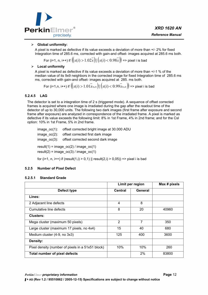
5.2.5.1 Standard Grade
Limit per region Max # pixels
Defect type Central General
Lines:
2 Adjacent line defects 4 8
Cumulative line defects 8 20 40960
Clusters:
Mega cluster (maximum 50 pixels) 2 7 350
Large cluster (maximum 17 pixels, no 4x4) 15 40 680
Medium cluster (4-9, no 3x3) 125 400 3600
Density:
Pixel density (number of pixels in a 51x51 block) 10% 10% 260
Total number of pixel defects 2% 83800

PerkinElmer proprietary information Page 13 P AS (Rev 1.2 / 95510862 / 2005-12-15) Specifications are subject to change without notice
HIS-Reference-Book Proprietary Information
XRD 1620 AN Reference Manual
5.2.5.2 CT-Grade
Limit per region Max # pixels
Defect type Central General
Lines:
2 Adjacent line defects 0 1
Cumulative line defects 5 11 22528
Clusters:
Mega cluster (maximum 36 pixels) 0 1 36
Large cluster (maximum 17 pixels, no 4x4) 5 20 340
Medium cluster (4-9, no 3x3) 50 200 1800
Density:
Pixel density (number of pixels in a 51x51 block) 10% 10% 260
Total number of pixel defects 1 % 40000

PerkinElmer proprietary information Page 14 P AS (Rev 1.2 / 95510862 / 2005-12-15) Specifications are subject to change without notice
HIS-Reference-Book Proprietary Information
XRD 1620 AN Reference Manual
5.3 Power supply XRD-EP The enhanced power supply XRD-EP is a stand-alone unit to support the XRD 1620 series. The power supply belongs to the protection class I and supports 100 V to 240 V at 47 Hz to 66 Hz. An LED Display indicates the status of the device. In case of “overload” the power supply must be switched off and can be switched on after a few minutes.
For any further information for the detector including warranty conditions please contact the party from where the product was purchased for after-sales service. If information is not available, please contact PerkinElmer Optoelectronics (page 32).
Light Status
Overload The Power Supply is overloaded. The power Supply has to be switched OFF.
Mains The power Supply is connected to mains.
DC-Output The DC-Output is ON.
Table 8 Status Lights of the XRD-EP
Fig. 6 Image of the Power Supply XRD-EP
PerkinElmer proprietary information Page 15 P AS (Rev 1.2 / 95510862 / 2005-12-15) Specifications are subject to change without notice
HIS-Reference-Book Proprietary Information
XRD 1620 AN Reference Manual
Specifications XRD-EP
Physical Dimension (L,W,H) 291 mm x 100 mm x 180 mm
Weight 6,56 kg
Input 100 Volts – 240 Volts AC 47 Hz – 66 Hz 3,3 Ampere max; 200 Watts
Output 5,5 Volts / 5 Ampere DC 12,5 Volts / 5 Ampere DC -12,5 Volts / 5 Ampere DC
Internal Fuse 4 Ampere / 250 Volts
Table 9 Electrical and Mechanical Specification of the XRD-EP
PIN Output 1 + 12,5 V (UA2) 2 NC 3 0 V Sensor (UA1) 4 +5,5 V Sensor (UA1) 5 +12,5 V Sensor (UA2) 6 -12,5 V Sensor (UA3) 7 NC 8 -12,5 V (UA1) 9 0 V 10 +5,5 V (UA1) 11 0 V Sensor (UA2, UA3) 12 0 V
Table 10 PIN assignment of power supply XRD-EP
Transportation / Storage Operation
Ambient temperature -10° to +70°C +0° to +70°C Derating > 50°C: 2.5%/K
Relative humidity 5% to 90% 5% to 90% Note: No condensation
Table 11 Environmental Considerations for the Power Supplies
PerkinElmer proprietary information Page 16 P AS (Rev 1.2 / 95510862 / 2005-12-15) Specifications are subject to change without notice
HIS-Reference-Book Proprietary Information
XRD 1620 AN Reference Manual
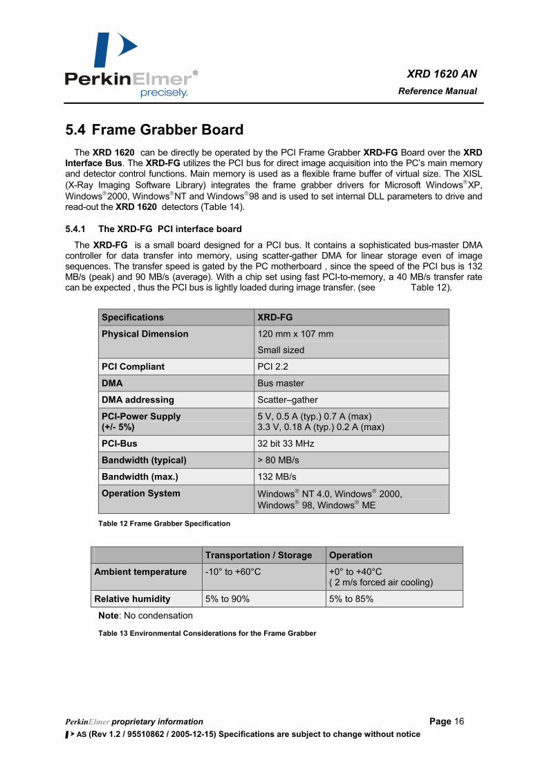
5.4 Frame Grabber Board The XRD 1620 can be directly be operated by the PCI Frame Grabber XRD-FG Board over the XRD Interface Bus. The XRD-FG utilizes the PCI bus for direct image acquisition into the PC’s main memory and detector control functions. Main memory is used as a flexible frame buffer of virtual size. The XISL (X-Ray Imaging Software Library) integrates the frame grabber drivers for Microsoft WindowsXP, Windows2000, WindowsNT and Windows98 and is used to set internal DLL parameters to drive and read-out the XRD 1620 detectors (Table 14).
5.4.1 The XRD-FG PCI interface board
The XRD-FG is a small board designed for a PCI bus. It contains a sophisticated bus-master DMA controller for data transfer into memory, using scatter-gather DMA for linear storage even of image sequences. The transfer speed is gated by the PC motherboard , since the speed of the PCI bus is 132 MB/s (peak) and 90 MB/s (average). With a chip set using fast PCI-to-memory, a 40 MB/s transfer rate can be expected , thus the PCI bus is lightly loaded during image transfer. (see Table 12).
Specifications XRD-FG
Physical Dimension 120 mm x 107 mm
Small sized
PCI Compliant PCI 2.2
DMA Bus master
DMA addressing Scatter–gather
PCI-Power Supply (+/- 5%)
5 V, 0.5 A (typ.) 0.7 A (max) 3.3 V, 0.18 A (typ.) 0.2 A (max)
PCI-Bus 32 bit 33 MHz
Bandwidth (typical) > 80 MB/s
Bandwidth (max.) 132 MB/s
Operation System Windows NT 4.0, Windows 2000, Windows 98, Windows ME
Table 12 Frame Grabber Specification
Transportation / Storage Operation
Ambient temperature -10° to +60°C +0° to +40°C ( 2 m/s forced air cooling)
Relative humidity 5% to 90% 5% to 85%
Note: No condensation
Table 13 Environmental Considerations for the Frame Grabber

PerkinElmer proprietary information Page 17 P AS (Rev 1.2 / 95510862 / 2005-12-15) Specifications are subject to change without notice
HIS-Reference-Book Proprietary Information
XRD 1620 AN Reference Manual
5.4.2 Connectors of the Frame Grabber
The connectors of the XRD-FG PCI interface board link the XRD 1620 detector to the personal computer. The female 50-PIN mini delta ribbon connector on the module can be used to plug in the Interface cable. The module allows data acquisition via the parallel interface, detector mode control via the serial configuration bus and generation of external triggering.
1 – /TRIG IN 2 – /FR_EN (Begin of frame) 3 – /FR_SYNC
Fig. 7 Image of the XRD-FG Frame Grabber
Two further HIIB signals, /FR_ENB and FR_SYNC, are also externally connectable as TTL signals (SMB-Subclic connectors). These two signals are capable of generating maskable interrupt requests in order to interrupt software support.
5.4.3 Installation of the Frame Grabber
To install the frame grabber the computer should be shut down, and the power supply unplugged. Failure to do so may cause severe damage to both the motherboard and frame grabber. In most cases the mainboard has an onboard LED which shows the power OFF mode or the soft-off mode (Power is still on). Hold the grabbers by the edges and do not to touch the chips, leads or connectors. Please place the frame grabber on a grounded antistatic pad whenever the grabbers are separated from the system. An exclusive IRQ port should be used, please consult the mainboard manual provided by the PC manufacture for more information. If more than one frame grabber has to be used in the system the switch on the left side of the grabber must be set to a unique number for every board, but please be aware that only one type of frame grabber can be used in one computer system. Please read the readme.txt on the installation CD for the latest information before installing the frame grabber driver and the application software.
Interface Bus

PerkinElmer proprietary information Page 18 P AS (Rev 1.2 / 95510862 / 2005-12-15) Specifications are subject to change without notice
HIS-Reference-Book Proprietary Information
XRD 1620 AN Reference Manual
5.4.3.1 Hardware Installation
1. Shut down the computer 2. Unplug the power supply and remove the computer system cover 3. Turn the switch of the grabber to a unique number for every board 4. Carefully align the frame grabber’s connectors and press firmly 5. Secure the card(s) on the slot with the screw 6. Replace the computer system’s cover 7. Restart the computer system 8. Log on to Windows using the administrator account
5.4.3.2 Installation of the XRD-FG on WindowsXP, Windows2000 or Windows98(ME)
1. After LOG ON the Hardware Wizard notice the new frame grabber as an multimedia device 2. Plug in the XIS Installation CD-ROM 3. Follow the hardware wizard to install the XRD-FG as a new device 4. After installation of the XRD-FG and XISL drivers by the Wizard start the XIS setup from the
appearing menu or if the Setup does not start automatically start the START.EXE in the root directory of the CD
5. The XIS SETUP program will lead you through the installation process 6. Restart the computer system 7. The XIS is now ready to start 8. If the initialization of the frame grabber and the detector is successful if a corresponding message
appears in the status bar.
5.4.3.3 Installation of the XRD-FG on WindowsNT
1. Plug in the XIS Installation CD-ROM 2. If the Setup does not start automatically start the START.EXE in the root directory of the CD 3. Select the XIS SETUP in the appearing menu 4. The SETUP program will lead you through the installation process 5. Select the XRD-FG as your favorite frame grabber 6. Restart the computer system The XIS is now ready to start 7. If the initialization of the frame grabber and the detector is successful a corresponding message
appears in the status bar.

PerkinElmer proprietary information Page 19 P AS (Rev 1.2 / 95510862 / 2005-12-15) Specifications are subject to change without notice
HIS-Reference-Book Proprietary Information
XRD 1620 AN Reference Manual
5.5 X-Ray Imaging Software Library (XISL) The X-Ray Imaging Software Library (XISL) allows implementation and use of all required detector functions into specific image processing software programs. The list below describes a selection of important routines. The routines can be easily integrated in any modular programmed software. Their specific use is described in the on-line help of the XIS program and the XIS Reference Book.
Command Module Explantation
Acquisition_Init Routine for general initialization of an XRD and Frame Grabber.
Acquisition_EnumSensors Enumerates all connected sensors
Acquisition_GetNextSensor Iterates through all recognized sensors.
Acquisition_Define_DestBuffers Definition of the required destination buffers for image capturing.
Acquisition_Acquire_Image_Ex General routine to acquire images from the detector.
Acquisition_Abort Stops image acquisition.
Acquisition_Close Frees all resources allocated for image acquisition.
Acquisition_Acquire_OffsetImage Allows acquisition of an Offset image for a specific or for all available frame times.
Acquisition_Acquire_GainImage Allows acquisition of a specific Gain image for a chosen frame time.
Acquisition_DoOffsetCorrection Routine corrects an image automatically with the actual Offset image.
Acquisition_DoOffsetGainCorrection_Ex Routine corrects an image automatically with the actual Gain image.
Acquisition_DoPixelCorrection Routine for an automatic pixel-wise mean correction with the loaded PxlMask map.
Acquisition_LoadPixelMap Load the map of defective pixels for Median correction.
Acquisition_CreateGainMap Create a List of Median values for the Multiple Gain-Correction
Acquisition_IsAcquiringData Checks if sensor is about to acquire images.
Acquisition_GetIntTime Routine to detect the actual frame time automatically.
Acquisition_SetReady Informs the XISL that image drawing is ready. If not ready a warning message is generated by XISL.

PerkinElmer proprietary information Page 20 P AS (Rev 1.2 / 95510862 / 2005-12-15) Specifications are subject to change without notice
HIS-Reference-Book Proprietary Information
XRD 1620 AN Reference Manual
Acquisition_GetReady Informs the user if image drawing is ready.
Acquisition_GetErrorCode If any of the XISL function returns with an error, extended information can be obtained.
Acquisition_GetConfiguration Retrieves the current configuration setting of the XISL.
Acquisition_SetCameraMode Allows setting of detector frame time. (not available for all detectors)
Acquisition_SetCameraGain Allows setting of detector sensitivity.
Acquisition_SetFrameSyncMode This function sets the synchronization mode of the frame grabber and detector
Acquisition_GetWinHandle Returns the currently set acquisition window handle (mostly main window).
Acquisition_GetActFrames Current acquisition frame.
Acquisition_GetAcqType Returns the currently used acquisition mode (single image, sequence, continuous, average and so on).
Acquisition_SetCorrData_Ex This function switches the correction buffers during a running acquisition.
Acquisition_GetCorrData_Ex This function retrieves the correction buffers during a running acquisition
Table 14 List of XISL modules

PerkinElmer proprietary information Page 21 P AS (Rev 1.2 / 95510862 / 2005-12-15) Specifications are subject to change without notice
HIS-Reference-Book Proprietary Information
XRD 1620 AN Reference Manual
5.5.1 Description of file header
The file header allows the use of specific information which can be implemented into any software.
Information Description
File header 68 byte
WORD FileType File ID (0x700)
WORD HeaderSize Size of this file header in bytes
WORD HeaderVersion yy.y
ULONG FileSize Size of the whole file in bytes
WORD ImageHeaderSize Size of the image header in bytes
WORD ULX, ULY, BRX, BRY bounding rectangle of the image
WORD NrOfFrames Number of Frames
WORD Correction 0 = none, 1 = Offset, 2 = Offset+Gain
Double IntegrationTime frame time in microseconds
WORD TypeOfNumbers frame time in milliseconds
WORD TypeOfNumbers short, long integer, float, signed/unsigned, inverted, fault map, Offset/Gain correction data, badpixel correction data
BYTE x[WINRESTSIZE] fill up to 68 byte
Table 15 File header description

PerkinElmer proprietary information Page 22 P AS (Rev 1.2 / 95510862 / 2005-12-15) Specifications are subject to change without notice
HIS-Reference-Book Proprietary Information
XRD 1620 AN Reference Manual
5.5.2 Interrupt sources
Interrupts allow the application to wait passively for changes in the acquisition status of the hardware. There are four interrupt sources:
• start of DMA • end of DMA • end of sequence • end of acquisition
These interrupts occur if the acquisition status changes to allow the application to react. The acquisition mode (Continuous, Single Shot, Sequence) influences the data flow and therefore the acquisition status. The following diagrams illustrate the data flow and the corresponding interrupts.
Fig. 8 Interrupt sources at a) sequence (4 frames) and b) continuous acquisition mode
DMA
DMA
DMA
DMA
End DMA IRQ
Application
Start DMA IRQ
Start DMA IRQ
End DMA IRQ
Start DMA IRQ
End DMA IRQ
Start DMA IRQ
End Acquisition End AcquisitionIRQ
StartAcquisition
End Sequence End SequenceIRQ
DMA
DMA
DMA
DMA
End DMA IRQ
Application
Start DMA IRQ
Start DMA IRQ
End DMA IRQ
Start DMA IRQ
End DMA IRQ
Start DMA IRQ
StartAcquisition
End SequenceIRQ
Verbinde
n
End Acquisition End AcquisitionIRQ
End DMA IRQ

PerkinElmer proprietary information Page 23 P AS (Rev 1.2 / 95510862 / 2005-12-15) Specifications are subject to change without notice
HIS-Reference-Book Proprietary Information
XRD 1620 AN Reference Manual
After the application has begun the acquisition, one interrupt is created by the beginning of DMA (start DMA interrupt). If the whole frame data is transferred the end of DMA interrupt is signaled. Both interrupts show the same behavior in all acquisition modes. If the end of DMA buffer is full, the resulting action depends on the acquisition mode. In sequence or single shot acquisition mode an end of sequence interrupt occurs and then an end of acquisition interrupt is created. In continuous acquisition mode an end of sequence interrupt is created and the data transfer is continuous at start of DMA buffer. If the acquisition is cancelled an end of acquisition interrupt is signaled. If interrupts are enabled the end of frame, end of sequence and the end of acquisition interrupts are used.
5.5.3 Sorting schemes overview
The XISL sorts the data in an internal buffer with highly optimized routines written in machine code. Fig. 9 shows the read out scheme of the XRD 1620 sensor.
Fig. 9 Sorting scheme of the XRD 1620
The sensor is divided into an upper and a lower part. Both sections are electrically separated. The data of each section is transferred by 16 ”read out groups” (ROG). Each ROG has 128 channels for the detector. The upper groups scan the sensor columns from left to right. The lower groups scan from right to left. The upper groups are transferred first, followed by the lower groups. The upper groups start read out from the upper row. The lower groups start read out from the last row. The following list displays the data stream for XRD 1620:
data stream no. sensor pixel (row, column) ROG no. 1 (1,1) 1 2 (1,129) 2 3 (1,257) 3 4 (1,385) 4 5 (1,513) 5 6 … 15 (1,1793) 15 16 (1,1921) 16 17 (2048,256) 18 18 (2048,128) 17 19 (2048,512) 20 20 (2048,384) 19 … … …
PerkinElmer proprietary information Page 24 P AS (Rev 1.2 / 95510862 / 2005-12-15) Specifications are subject to change without notice
HIS-Reference-Book Proprietary Information
XRD 1620 AN Reference Manual
6 Operational Functions
6.1 Getting Started - The first image
6.1.1 Introduction
This chapter describes the procedures to obtain initial x-ray images with adequate quality. It explains how correction files are used with appropriate settings of the detector integration time and x-ray source parameters. In this example the Demo Software XIS is used to describe the mechanism. The XIS is intended to be used for demonstration purposes only and should not to be used as standard software detector operation. Detailed information about the XIS and the XISL are provided in the XIS-Reference Book.
6.1.2 General considerations
In principal the detector can produce images without any correction. These images contain the offset of the readout electronics, the individual offsets of each pixel (dark current) as well as the electronics and pixel gain differences, apart from the x-ray source non-uniformities. Each column is connected to one channel of the readout electronics with the specific channel offset resulting in a dark image with vertical stripes caused by the individual channel offsets. The dark image may also contain pixels which are brighter than the others caused by a higher dark current. The detector is arranged in groups of 128 readout channels. The groups can deviate in their gain such that one can distinguish blocks of 128 channels in a bright image caused by this gain difference. The panel itself may contain pixels and perhaps row or columns which are defective (completely black or white). To eliminate these detector specific effects and obtain good quality results, each image will be ‘offset’ and ‘gain’ corrected, and if required, the defective pixels will also be corrected. The creation of the correction files is described in the chapter How to perform corrections.
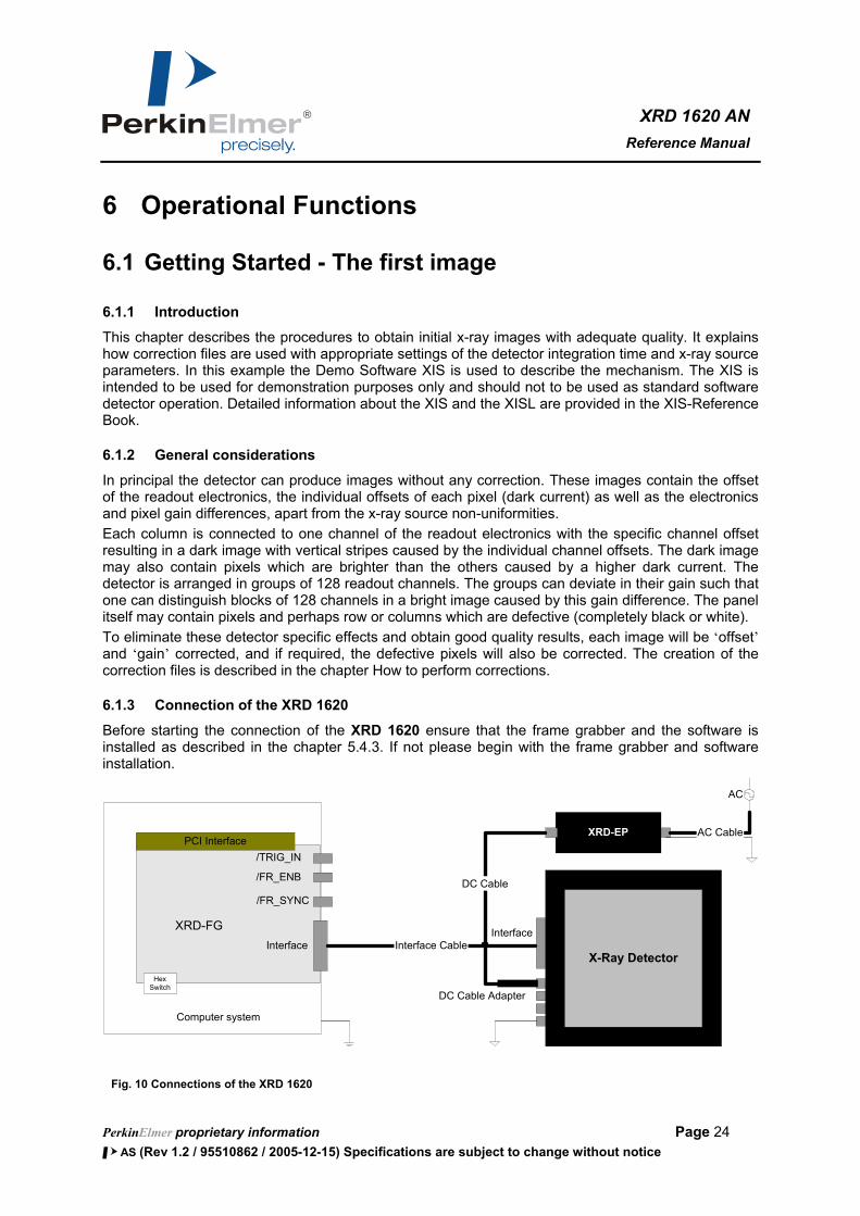
6.1.3 Connection of the XRD 1620
Before starting the connection of the XRD 1620 ensure that the frame grabber and the software is installed as described in the chapter 5.4.3. If not please begin with the frame grabber and software installation.
Interface
/TRIG_IN
/FR_ENB
/FR_SYNC
PCI Interface
HexSwitch
XRD-FG InterfaceInterface Cable
XRD-EP
X-Ray Detector
DC Cable
AC
AC Cable
DC Cable Adapter
Computer system
Fig. 10 Connections of the XRD 1620

PerkinElmer proprietary information Page 25 P AS (Rev 1.2 / 95510862 / 2005-12-15) Specifications are subject to change without notice
HIS-Reference-Book Proprietary Information
XRD 1620 AN Reference Manual
The computer with the frame grabber and the monitor need to be grounded through the protection earth conductors within the power cords. The required potential equalization of the XRD 1620 and the XRD-EP power supply has to be managed through the labeled connectors and the potential equalization between both devices is managed through the XRD-EP DC Cable and XRD-EP DC Adapter. For safety reasons only original cables and connectors should be used.
The XRD 1620 should be connected as described in the following manner and as shown in Fig. 10
1. Shut down the computer 2. Connect the XRD 1620 and the XRD-EP with the potential equalization 3. Connect the Frame Grabber and the XRD 1620 via Interface Cable 4. Connect the DC Cable Adapter with the Power Connector of the XRD 1620 5. Connect the XRD-EP and the DC Cable Adapter via DC Cable 6. Connect the XRD-EP with the power supply via AC Cable. 7. Switch on the XRD-EP 8. Switch on the Computer
6.1.4 The first image
The detector is powered on and all cables connected. At startup the frame grabber board will be initialized and afterwards a dialog box is displayed in order to select the mode of the frame grabber board. ”Yes” enables the Interrupt Mode and ”No” the Polling Mode. In both cases the system attempts to initialize the frame grabber board(s) and the detector. The ”Cancel” button starts the program without initialization. The initialization can take some time depending on the number of frame grabber boards and detectors. If more than one detector is connected a dialog box is displayed containing a list of all recognized detectors An active detector has to be selected, and all following actions will correspond to the active detector . The system is now ready to acquire the first image. The Acquire\Single Shot command acquires a single image. If the detector was not irradiated only a dark image is displayed. The image can be enhanced by the brightness and contrast settings. As explained above, the uncorrected dark image contains vertical stripes caused by the electronics offset. By choosing the Continuous acquisition mode the image is refreshed on the display in the selected frame rate. In the next step the detector should run in the continuous mode and the x-ray source should be switched on to irradiate the detector. The brightness and contrast should be set to default (F2-KEY: 0-65535). If a gray image is displayed, the parameters of the x-ray source and detector are within appropriate limits. If a white or a black image is displayed the x-ray source needs to be adjusted accordingly.
6.2 How to perform corrections The X-Ray Detector works as an independent detector to acquire X-ray images. After starting the XIS.EXE software, the detector is automatically initialized and provides images in the fastest setting (TIMING 0) (Timings menu: list of possible frame times). The X-Ray Detectors need an Offset correction to account for the dark current of each pixel. In particular, during the warm-up phase of the detector, the Offset correction should be repeated periodically. Periodic refresh of the Offset correction is required during operation in order to meet the full performance specifications. Additionally, a Gain correction is required to homogenize differences in pixel sensitivities and to take into account the X-ray beam illumination. It is therefore very important that the whole image area is illuminated homogenously. The Gain correction should be applied under optimum dynamic range (70-80 % of the full scale range FSR) or in the dynamic range of interest. The radiation intensity used to create the gain image can depend on the application, e.g. if the typical grey level is about 10.000 ADU

PerkinElmer proprietary information Page 26 P AS (Rev 1.2 / 95510862 / 2005-12-15) Specifications are subject to change without notice
HIS-Reference-Book Proprietary Information
XRD 1620 AN Reference Manual
and the remaining area is saturated, it is recommended to use a gain created at 10.000 ADU. The use of an Offset corrected Gain calibration eliminates offset dependency and therefore any stored Gain correction can be used for a specific frame time for longer time periods. The image performance can be enhanced by using the Multiple Gain Correction. For each dynamic range of interest a separate offset corrected and averaged bright image is used as an interpolation point. The maximum number of interpolation points depends on the installed computer memory. It is important that each bright image is completely and homogenously illuminated. The Pixel correction allows a ‘software repair’ of defective pixels to enhance image quality. Improper pixel values are replaced with the averaged value of the surrounding eight adjacent pixels where defective pixels are not used. The pixel correction is only performed on specific pixels, mapped in the file PXLMASK.HIS. Each detector is shipped from PerkinElmer with the PXLMASK.HIS file for that specific detector The user can also generate a correction file. Please be aware that the number of pixels used for the mean correction should be minimized. The pixel correction procedure requires CPU time and depending on its speed, a slower presentation of the acquired images on screen may occur depending on the selected timing mode of the system. The main screen of the XIS software displays a warning message if all of the acquired images are not accepted by the computer.
Note:To fully meet all performance specifications, all corrections and the correction files must be acquired at the same readout mode, gain setting and integration time as the images to be corrected
6.2.1 Use of the Offset Correction
The offset correction of images should be used to eliminate the effects of pixel dark currents on the acquired image. To obtain an Offset correction file the following steps are required: 1. Select the desired integration time, readout mode and gain setting. 2. Switch off the X-ray source so that the detector only transfers its ”dark image”. 3. Wait a few seconds until the detector archives an equilibrium. 4. Start the Get Offset Image. / Start All Offset Images. 5. Select a number of frames.
It is recommended to use between 20 to 100 frame cycles which will be averaged. The averaged image is qualified as the new Offset Image of the selected frame time and automatically linked to later acquired images.
6. Control the new acquired image using the Options/View command and/or Brightness, Contrast or LUT range.
7. The Offset correction file can be saved if desired. Note: A warning appears if the program is quit without saving new acquired Offset correction files.
The Offset correction should be repeated periodically in order to meet the full performance specifications. In particular during the warming-up period of the system, the dark current of the pixels may change considerably. To interrupt the procedure the <ESC> key can be used.
NOTE: If the item Get All Offset Images is used, step 4 is automatically performed for all available frame times. Please check the total time necessary before selecting the number of frames to avoid longer waiting periods.

PerkinElmer proprietary information Page 27 P AS (Rev 1.2 / 95510862 / 2005-12-15) Specifications are subject to change without notice
HIS-Reference-Book Proprietary Information
XRD 1620 AN Reference Manual
6.2.2 Use of the Gain/Offset Correction
The Gain/Offset correction of images is used to eliminate the effects of pixel sensitivities and the X-ray source on the acquired image. To obtain a Gain/Offset correction file the following steps are required: 1. Select the desired integration time, readout mode and gain setting. 2. Acquire a new Offset correction image. 3. Switch on the X-Ray source and adjust the brightness of the acquired image in the desired read
out settings. The detector’s acquired intensity should be between 70-80 % of FSR or in the dynamic range of the ROI. The gain intensity depends on the application, but the entire image area should be illuminated homogenously.
4. Start the Get Gain/Offset Image. 5. Select a number of frames.
20 to 100 frame cycles should be used which will be averaged. The averaged image is implemented as the new Gain/Offset Image of the selected frame time and automatically linked to later acquired images.
6. Adjust the new acquired image by using the Options/View command and/or Brightness, Contrast or LUT range.
7. Store the Offset correction file if desired. Note: A warning appears if the program is quit without saving new acquired Offset correction files.
To interrupt the procedure the <ESC> key can be used.
NOTE: The Gain image is automatically Offset corrected with the currently linked Offset correction file. To obtain best quality of the correction file, please perform a new Offset correction before starting Gain/Offset correction.
6.2.3 Use of Multiple Gain Correction
The Multiple Gain Correction is used to eliminate the effects of pixel sensitivities and the X-ray source on the acquired image. To obtain a Multiple Gain Correction file the following steps are required: 1. Select the desired integration time, readout mode and gain setting 2. Acquire a new Offset correction image. 8. Switch on the X-Ray source and adjust the brightness of the acquired image in the desired read
out settings. The detector’s acquired intensity should be in the dynamic range of the ROI. The whole image should be illuminated homogenously.
3. Start the Acquire Sequence 4. Select a number of frames and the average mode.
20 to 100 frame cycles should be used which will be averaged. 5. Adjust the new acquired image by using the Options/View command and/or Brightness, Contrast
or LUT range. 6. Store the Offset corrected bright image 7. Repeat the steps 3-7 for each intensity of interest. 8. Create a Gain –Sequence with Acquire=>Build Gain Sequence 9. Start a new acquisition. 10. Link the created Gain-Sequence file with Acquire=>Link Gain Sequence 11. Store the Offset correction file if desired.
Note: A warning appears if the program is quit without saving new acquired Offset correction files.

PerkinElmer proprietary information Page 28 P AS (Rev 1.2 / 95510862 / 2005-12-15) Specifications are subject to change without notice
HIS-Reference-Book Proprietary Information
XRD 1620 AN Reference Manual
6.2.4 Use and generation of the Pixel Correction
The Pixel Correction of images is used to eliminate the effects of defective pixels of the detector on acquired images. To get an Pixel correction file the following steps have to be performed: 1. Select the desired frame time (see Timings menu). 2. Link correction files. 3. Switch on the X-ray source and in the continuous mode, adjust the brightness of the acquired
image. The detector’s acquired intensity should be between 70-80 % of its maximum signal. 4. Start an image acquisition as for the Get Gain/Offset Image (no sample in front of the detector). 5. Adjust the new acquired image by using the Options/View command and/or Brightness, Contrast
or LUT range. 6. The window should show an homogenous corrected image. Intensity deviations are the result of
marginal pixels. 7. Adjust the x-ray source such that the detector’s acquired intensity should be about 50 % of its
maximum signal. 8. Go to Select by Value in the Edit Menu. 9. Enter desired range of good pixels (e.g. 15000-45000 out of 0-65535) 10. Select ”Out of range” button. (All selected pixels are marked.) 11. Call Create Pixel Map in the Edit Menu. 12. The Pixel Map is created and can be stored as new PXLMASK.HIS.
NOTE: The new PXLMASK.HIS is automatically linked to new acquisitions and the acquired start-up image (see 4.) is also corrected.
6.2.5 Correct previously acquired images
It is possible to correct previously acquired uncorrected images by selecting the desired image by the Window Command and use one of the Link Commands (Link Offset Correction, Link Gain Correction or Link Pixel Correction). The active image is automatically corrected. These settings are also used for the next acquisitions.
NOTE: It is not recommended to close linked correction files during a running acquisition. This can cause the application to close.
6.3 How to RUN the Detector
6.3.1 Free Running
Eight different frame times are available and the detector automatically starts in the first free running timing (Timing 0) which is the fastest readout time. This means that the detector needs a minimum of 285. ms (XRD 1620) for one frame. Each pixel is readout every 285. ms and during this time the pixel integrates radiation. For details of the readout scheme see the chapter Sorting. The structure of higher timings is a first readout using the slowest readout time and a following delay. To realize delay using the fastest readout, use the internal trigger mode with a frame time of the selected timing plus the delay time.

PerkinElmer proprietary information Page 29 P AS (Rev 1.2 / 95510862 / 2005-12-15) Specifications are subject to change without notice
HIS-Reference-Book Proprietary Information
XRD 1620 AN Reference Manual
6.3.2 Internal Trigger
If a pulsed x-ray source is used exposure should occur during the delay of the detector since the x-ray pulse appears during the readout time the information is split into two frames. In addition if these frames are summarized there could be artifacts which are not correctable. In order to expose during the delay the detector allows triggering of the x-ray source and the detector itself.
t1
t5
/FR_EN
/LN_ENheader
/TRIG_OUT
t2
t3
t4
t6 t6
t5
t8
t7
first data line last data line
T
t9
Fig. 11 General timing diagram in continuous mode
6.3.3 External Trigger
Triggering the detector attempts to synchronise the detector to other devices e.g. x-ray sources having specific schemes of radiating x-ray pulses. The current mode is triggering the detector on a frame basis, meaning the detector sends a frame after triggering by an external pulse and ignores all other incoming pulses until the selected frame time has elapsed. After that the detector can be triggered by a new pulse. In order to trigger the detector a 20 µs wide low active trigger pulse (LVDS-signal) has to be transmitted to the device. The trigger signal has to be generated externally and can then be connected to the 7-pin round connector, (/TRIG_IN) located directly at the detector device, or connected to the sub-click located on the rear side of the frame grabber (/TRIG_IN converted to RS422 signal as /FR_SYNC). Trigger pulses are accepted from both sources. Prior to this the detector has to be set by command into the external trigger mode. The waveform of the trigger pulse as shown in Fig. 12 describes the triggering mode on a frame by frame basis. The period of the trigger waveform determines the integration time. The /TRIG_OUT signal with a pulse width of 62.5 ns indicates the start of a new frame and can be used to synchronise the x-ray source.
t1
t5
/FR_EN
/LN_ENheader
/TRIG_OUT
t2 t3
t4
t6 t6
t5
t8
tc
first data line last data line
t9
/TRIG_IN
ta tb
Tp
ta
td
Fig. 12 General timing diagram in triggered mode
PerkinElmer proprietary information Page 30 P AS (Rev 1.2 / 95510862 / 2005-12-15) Specifications are subject to change without notice
HIS-Reference-Book Proprietary Information
XRD 1620 AN Reference Manual
6.3.4 Internal Trigger
The internal trigger mode works in the same way as the external trigger mode, and also triggers the detector on a frame by frame basis. This means that the detector sends a frame after triggering by an external pulse and ignores all other incoming pulses until the selected frame time has elapsed. After that the detector can be triggered by a new pulse. The trigger pulse is supported by the frame grabber and is a fixed pulse with frequency of between the fastest free running mode of the detector and 5 seconds, in steps of 1µs. The frame grabber sends the RS422 signal /FR_SYNC over the HIIB to the detector. The /TRIG_OUT signal with a pulse width of 62.5 ns indicates the start of a new frame and can be used to synchronise the x-ray source.
6.3.5 How to use the internal trigger mode
The following method describes how the internal trigger can be used to implement different integration times or to use one of the readout schemes with an customized delay. If the Interface Bus is connected and the power is switched on the detector runs in the first free running mode. To use the internal trigger mode the following steps are required:
1. The detector is set to the desired readout time using the Timings menu XISL: Acquisition_SetCameraMode(hAcqDesc, 0..7) -> The detector runs continuously (free running) in the desired timing and readout scheme.
2. The detector is set to the internal trigger mode using the Detector Mode menu XISL: Acquisition_SetFrameSyncMode(hAcqDesc, HIS_SYNCMODE_INTERNAL_TIMER). -> The detector aborts the current frame and waits for a trigger signal. -> The shortest repeat time of an trigger pulse is the selected timing (readout time).
3. Select the frame rate (readout plus delay time) in the appearing dialog (readout time … 5s) XISL: Acquisition_SetTimerSync(hAcqDesc, frame_rate).
4. The frame grabber sends the /FR_SYNC signal directly via the HIIB to the detector in the selected frame rate. -> The detector runs “continuously” with the selected frame rate.
5. Start the acquisition XISL: Acquisition_AquireImage(hAcqDesc, frames, …) -> The frame grabber places the data into the memory.

PerkinElmer proprietary information Page 31 P AS (Rev 1.2 / 95510862 / 2005-12-15) Specifications are subject to change without notice
HIS-Reference-Book Proprietary Information
XRD 1620 AN Reference Manual
6.4 How to use the detector gain setting This paragraph describes how to change the detector gain setting. The XRD 1620 AN supports up to 5 different gain settings (Table 16). When the detector is powered on the XRD 1620 AN runs with 1pF capacity. The detector gain will be set bitwise by the XIS dialog Options/Detector Options or by the library function Acquisition_SetCameraGain(hAcqDesc, 1..5). The Table 16 will give an overview of the different gain settings. It is very important for the image quality that the correction files were obtained in the same gain setting as in the current working operating mode.
Selected Value Capacity 1 0,5 pF 2 1 pF 3 2 pF 4 4 pF 5 8 pF
Table 16 Overview of the five Detector Gain Settings
6.5 Maintenance In principle the detector assembly is maintenance-free. However it is important that all correction files are regularly updated and used for image processing. In some applications it is advantageous to update the offset correction file directly before each image. Although the a-Si detectors are resistant to x-rays they can exhibit degradation over time when exposed to high X-Ray dose environments. Sensitivity and uniformity may change depending on the weekly exposure duration and X-Ray dose. Therefore the pixel correction files should be checked and compared regularly to determine changes in bad pixels and clusters.
6.6 Disposal This label on the product and its literature indicates that it should not be disposed with other waste at the end of its working life. To prevent possible harm to the environment or human health from uncontrolled waste disposal please separate this from other types of waste and recycle it responsibly to promote the sustainable reuse of material resources.
Please contact your supplier or distributor and check the terms of conditions of the purchase contract. This product should not mixed with other commercial wastes for disposal.

PerkinElmer proprietary information Page 32 P AS (Rev 1.2 / 95510862 / 2005-12-15) Specifications are subject to change without notice
HIS-Reference-Book Proprietary Information
XRD 1620 AN Reference Manual
7 After-Sales Service for PerkinElmer Products Please contact your distributor for after-sales service (including warranty conditions) or any other information. In case information is not available, please contact one PerkinElmer Optoelectronics subsidiaries (regional service headquarters) listed below. For product returns, please contact your distributor or PerkinElmer Optoelectronics for shipping and packaging instructions. Please do not return product to PerkinElmer Optoelectronics for repair without advance notification. USA PerkinElmer Optoelectronics 2175 Mission College Boulevard Santa Clara, CA 95054 Telephone: +1 408-565-0850 Email: [email protected] Europe PerkinElmer Optoelectronics Wenzel-Jaksch-Str. 31 D-65199 Wiesbaden Germany Telehone: +49 611 492 430 Fax: +49 611 942 165 Email: [email protected] ASIA PerkinElmer Optoelectronics 47 Ayer Rajah Crescent #06-12 Singapore 139947 Telephone: +65 6775 2022 Email: [email protected]

PerkinElmer proprietary information Page 33 P AS (Rev 1.2 / 95510862 / 2005-12-15) Specifications are subject to change without notice
HIS-Reference-Book Proprietary Information
XRD 1620 AN Reference Manual
8 Guidance and Manufacturer’s Declaration Guidance and Manufacturer’s Declaration of Electromagnetic Emissions The X-Ray Detector is intended for use in the electromagnetic environment specified below. The customer or the user of the X-Ray Detector should assure that it is used in such an environment.
Emissions test Compliance Electromagnetic Environment – Guidance
RF-emissions CISPR 11 Group 1 The X-Ray Detector uses RF energy only for its internal function. Therefore, its RF emissions are very low and are not likely to cause any interference in nearby electronic equipment.
RF-emissions CISPR 11 Class B
Harmonic emissions IEC 61000-3-2 Class A
Voltage fluctuations/ flicker emissions IEC 61000-3-3 Complies
The X-Ray Detector is suitable for use in all establishments, including domestic establishments and those directly connected to the public low-voltage power supply network that supplies buildings used for domestic purposes.
Table 17 Guidance and Manufacturer’s Declaration of Electromagnetic Emissions
Guidance and Manufacturer’s Declaration of Electromagnetic Immunity The X-Ray Detector is intended for use in the electromagnetic environment specified below. The customer or the user of the X-Ray Detector should assure that it is used in such an environment.
Immunity Test IEC 60601 Test Compliance Electromagnetic Environment – Guidance
Electrostatic Discharge (ESD) ICE 61000-4-2
Contact: 6 kV Air: 8 kV
Contact: 6 kV Air: 8 kV
Floors should be made of wood, concrete, or ceramic tile. If floors are covered with synthetic material, the relative humidity should be at least 30%.
Electrical fast transients (Burst) ICE 61000-4-4
0.5 kV (AC) 1kV (DC)
0.5 kV (AC) 1kV (DC)
Mains power quality should be that of a typical commercial and/or hospital environment.
Transients-Surges ICE 61000-4-5 1 kV / 2 kV 1 kV / 2 kV Mains power quality should be that of a typical
commercial and/or hospital environment.
Power frequency magnetic fieldICE 61000-4-8 3 A/m 3 A/m
Power frequency magnetic fields should be at levels characteristic of a typical location in a typical commercial and/or hospital environment.
Voltage dips and short interruptions ICE 61000-4-11
-95% / 10 ms
-60% / 100 ms
-30% / 500 ms
>-95% / 5000 ms
-95% / 10 ms
-60% / 100 ms
-30% / 500ms
>-95% / 5000 ms
Mains power quality should be that of a typical commercial or hospital environment.
If the user of the X-Ray Detector requires continued operation during power mains interruptions, it is recommended that the X-Ray Detector be powered from an uninterruptible power supply or battery.
Table 18 Guidance and Manufacturer’s Declaration of Electromagnetic Immunity

PerkinElmer proprietary information Page 34 P AS (Rev 1.2 / 95510862 / 2005-12-15) Specifications are subject to change without notice
HIS-Reference-Book Proprietary Information
XRD 1620 AN Reference Manual
Guidance and Manufacturer’s Declaration of Electromagnetic Immunity The X-Ray Detector is intended for use in the electromagnetic environment specified below. The customer or the user of the X-Ray Detector should assure that it is used in such an environment.
Immunity Test IEC 60601 Test Compliance Electromagnetic Environment – Guidance
Conducted radio-frequency fields (CEF) ICE 61000-4-6
Radiated electromagnetic field (REF) ICE 61000-4-3
3 V
150 kHz to 80 MHz
3 V/m
80 MHz to 2.5 GHz
[V1] 3 V
150 kHz to 80 MHz
[E1] 3 V/m
80 MHz to 2.5 GHz
Portable and mobile RF-communication equipment should no closer to any part of the X-Ray Detector including the data cables, than the recommended separation distance calculated from the equation appropriate for the frequency of the transmitter
PV
d1
5.3=
PE
d1
5.3= ,for 80 MHz to 800 Mhz
PE
d1
7= ,for 800 MHz to 2.5 Ghz
using P as the maximum output of the transmitter in watt (W) according to the transmitter manufacture and d as the recommended separation distance in meter (m).
Field strengths outside the shielded location from fixed RF transmitters, as determined by an electromagnetic site surveya, should be less than 3 V/m.
Interference may occur in the vicinity of equipment marked with the following symbol:
NOTE 1 These guidelines may not apply all situations. Electromagnetic propagation is affected by absorption and reflection from structures, objects and people.
NOTE 2 It is essential that the actual shielding effectiveness and filter attenuation of the shielded location be verified to assure that they meet the minimum specification. a Field strengths from fixed transmitters, such as base stations for radio (cellular/cordless) telephones and land mobile radios, armature radio, AM and FM radio broadcast and TV broadcast cannot be predicted theoretically with accuracy. To assess the electromagnetic environment due to fixed RF transmitters, an electromagnetic site survey should be considered. If the measured field strength in the location in which the X-Ray Detector is used exceeds the applicable RF compliance level above, the XRD should be observed to verify normal operation. If abnormal performance is observed, additional measures may be necessary, such as re-orienting or relocating the X-Ray Detector.
Table 19 Guidance and Manufacturer’s Declaration of Electromagnetic Immunity (Portable Equipment)

PerkinElmer proprietary information Page 35 P AS (Rev 1.2 / 95510862 / 2005-12-15) Specifications are subject to change without notice
HIS-Reference-Book Proprietary Information
XRD 1620 AN Reference Manual
Recommended Separation Distance between Portable and Mobile RF-Communication Equipment and the X-Ray Detector The X-Ray Detector is intended for use in the electromagnetic environment specified below. The customer or the user of the X-Ray Detector should assure that it is used in such an environment.
Rated Maximum Output Power of the Transmitter
(W)
150 kHz to 80 MHz
PV
d1
5.3=
80 MHz to 800 MHz
PE
d1
5.3=
800 MHz to 2.5 GHz
PE
d1
7=
0,01 0.12 0.12 0.23
0,1 0.38 0.38 0.73
1 1.2 1.2 2.3
10 3.8 3.8 7.3
100 12 12 23
For transmitter rated at a maximum output power not listed above, the separation distance can be estimated using the equation in the corresponding column, where P is the maximum output (power rating of the transmitter in watt (W)) according to the transmitter manufacture and d as the recommended separation distance in meter (m)..
Note: These guideline may not apply in all situations. Electromagnetic propagation is absorption and reflection from structures, objects, and people.
Table 20 Recommended Separation Distance between Portable and Mobile RF-Communication Equipment and the X-Ray Detector

PerkinElmer proprietary information Page 36 P AS (Rev 1.2 / 95510862 / 2005-12-15) Specifications are subject to change without notice
HIS-Reference-Book Proprietary Information
XRD 1620 AN Reference Manual
Related Documents