Exar Corporation 48720 Kato Road, Fremont CA, 94538 • (510) 668-7000 • FAX (510) 668-7017 • www.exar.com XR17V258 66MHZ PCI BUS OCTAL UART WITH POWER MANAGEMENT SUPPORT AUGUST 2010 REV. 1.0.2 GENERAL DESCRIPTION The XR17V258 1 (V258) is a single chip 8-channel 66MHz PCI (Peripheral Component Interconnect) UART (Universal Asynchronous Receiver and Transmitter) solution, optimized for higher performance and lower power. The V258 device with its fifth generation register set is designed to meet the high bandwidth and power management requirements for multi-serial communication ports for system administration and management. The 32-bit 66MHz PCI interface is compliant with PCI 3.0 and PCI power management revision 1.1 specifications. The device provides an upgrade path for Exar’s 33MHz 5V and Universal PCI UART family of products in a 144-pin LQFP package. The V258 consists of eight independent UART channels, each with set of configuration and enhanced registers, 64 bytes of Transmit (TX) and Receive (RX) FIFOs, and a fractional Baud Rate Generator (BRG). A global interrupt source register provides a complete interrupt status indication for all 8-channels to speed up interrupt parsing. The V258 device operates at 33/66MHz and features fully programmable TX and RX FIFO level triggers, automatic hardware and software flow control, and automatic RS-485 half duplex direction control output for software and hardware design simplification. NOTE 1: Covered by U.S. Patents #5,649,122 and #5,949,787 APPLICATIONS • Remote Access Servers • Storage Network Management • Factory Automation and Process Control • Instrumentation • Multi-port RS-232/RS-422/RS-485 Cards • Point-of-Sale Systems FEATURES • High performance 32-bit 66MHz PCI UART • PCI 3.0 compliance • PCI power management rev. 1.1 compliance • EEPROM interface for PCI configuration • 3.3V supply with 5V tolerant non-PCI (serial) inputs • Data read/write burst operation • Global interrupt register for all eight UART channels • Up to 8 Mbps serial data rate • Eight multi-purpose inputs/outputs • A 16-bit general purpose timer/counter • Sleep mode with wake-up Indicator • Eight independent UART channels controlled with ■ 16C550 compatible register set ■ 64-byte TX and RX FIFOs with level counters and programmable trigger levels ■ Fractional baud rate generator ■ Automatic RTS/CTS or DTR/DSR hardware flow control with programmable hysteresis ■ Automatic Xon/Xoff software flow control ■ RS-485 half duplex direction control output with selectable turn-around delay ■ Infrared (IrDA 1.0) data encoder/decoder ■ Programmable data rate with prescaler FIGURE 1. BLOCK DIAGRAM OF THE XR17V258 C/BE#[3:0] PAR FRAME# TRDY# IRDY# STOP# DEVSEL# IDSEL# 33/66MHz CLK RST# PERR# SERR# PME# EECK EEDI EEDO EECS TMRCK XTAL2 XTAL1/CLK RX[7:0] TX[7:0] RTS#[7:0] DTR#[7:0] CTS#[7:0] DSR#[7:0] DCD#[7:0] RI#[7:0] ENIR INTA# Global Configuration Registers Global Configuration Registers Crystal Osc/Buffer Crystal Osc/Buffer PCI Local Bus Interface Configuration Space Registers Multi-purpose Inputs/Outputs Multi-purpose Inputs/Outputs 16-bit Timer/Counter 16-bit Timer/Counter UART Channel 0 IR ENDEC UART Channel 0 64-byte TX FIFO 64-byte RX FIFO BRG IR ENDEC TX & RX UART Regs AD[31:0] C/BE#[3:0] C/BE#[3:0] PAR FRAME# TRDY# IRDY# STOP# DEVSEL# IDSEL# 33/66MHz CLK RST# PERR# SERR# PME# EECK EEDI EEDO EECS UART Channel 1 UART Channel 2 UART Channel 3 UART Channel 4 UART Channel 5 UART Channel 6 UART Channel 7 TMRCK XTAL2 XTAL1/CLK RX[7:0] TX[7:0] RTS#[7:0] DTR#[7:0] CTS#[7:0] DSR#[7:0] DCD#[7:0] MPIO[7:0] RI#[7:0] ENIR EEPROM Interface EEPROM Interface INTA#

Welcome message from author
This document is posted to help you gain knowledge. Please leave a comment to let me know what you think about it! Share it to your friends and learn new things together.
Transcript
XR17V25866MHZ PCI BUS OCTAL UART WITH POWER MANAGEMENT SUPPORT
AUGUST 2010 REV. 1.0.2
GENERAL DESCRIPTION
The XR17V2581 (V258) is a single chip 8-channel 66MHz PCI (Peripheral Component Interconnect) UART (Universal Asynchronous Receiver and Transmitter) solution, optimized for higher performance and lower power. The V258 device with its fifth generation register set is designed to meet the high bandwidth and power management requirements for multi-serial communication ports for system administration and management. The 32-bit 66MHz PCI interface is compliant with PCI 3.0 and PCI power management revision 1.1 specifications. The device provides an upgrade path for Exar’s 33MHz 5V and Universal PCI UART family of products in a 144-pin LQFP package.The V258 consists of eight independent UART channels, each with set of configuration and enhanced registers, 64 bytes of Transmit (TX) and Receive (RX) FIFOs, and a fractional Baud Rate Generator (BRG). A global interrupt source register provides a complete interrupt status indication for all 8-channels to speed up interrupt parsing. The V258 device operates at 33/66MHz and features fully programmable TX and RX FIFO level triggers, automatic hardware and software flow control, and automatic RS-485 half duplex direction control output for software and hardware design simplification.NOTE 1: Covered by U.S. Patents #5,649,122 and #5,949,787
APPLICATIONS
• Remote Access Servers• Storage Network Management
Exar Corporation 48720 Kato Road, Fremont CA, 94538 • (5
• Factory Automation and Process Control• Instrumentation• Multi-port RS-232/RS-422/RS-485 Cards• Point-of-Sale Systems
FEATURES
• High performance 32-bit 66MHz PCI UART• PCI 3.0 compliance• PCI power management rev. 1.1 compliance• EEPROM interface for PCI configuration• 3.3V supply with 5V tolerant non-PCI (serial) inputs• Data read/write burst operation• Global interrupt register for all eight UART channels• Up to 8 Mbps serial data rate• Eight multi-purpose inputs/outputs• A 16-bit general purpose timer/counter• Sleep mode with wake-up Indicator• Eight independent UART channels controlled with
■ 16C550 compatible register set■ 64-byte TX and RX FIFOs with level counters
and programmable trigger levels■ Fractional baud rate generator■ Automatic RTS/CTS or DTR/DSR hardware
flow control with programmable hysteresis■ Automatic Xon/Xoff software flow control ■ RS-485 half duplex direction control output
with selectable turn-around delay■ Infrared (IrDA 1.0) data encoder/decoder■ Programmable data rate with prescaler
FIGURE 1. BLOCK DIAGRAM OF THE XR17V258
Glo b a lC o n fig u ratio n
R eg is te rs
C rysta l Osc /B u ffer
PC I L o ca lBu s
Int erfa ce
C onfigurationS pace
R e giste rs
M u lti -p u rp o seIn p u ts /Ou tp u ts
16-bitT ime r/C ounte r
U AR T C h an nel 0
64-b yte TX F IFO
64-b yte RX F IFOBR G
IREN D E CTX & RX
UA RTRe gs
AD [31 :0]
C /B E #[3:0]
P ARF R AM E #
T R D Y#IR D Y#
S T O P #D E VS E L #
ID S E L #
33 /66M H z CL KR S T #
P E RR #S E RR #
P M E #
E E CKE E D I
E E D OE E CS
U AR T C h a n nel 1
U AR T C h a n nel 2
U AR T C h a n nel 3
U AR T C h a n nel 4
U AR T C h a n nel 5
U AR T C h a n nel 6
U AR T C h a n nel 7
T M R C KX T AL 2X T AL 1 /C L K
R X [7:0]
T X [7:0]
R TS #[7:0]
D TR #[7:0]
C TS #[7:0]
D S R #[7:0]
D C D #[7:0]
M P IO [7:0]
R I#[7:0]
E N IR
E E PR O MIn terfac e
IN T A#
Glo b a lC o n fig u ratio n
R eg is te rs
Glo b a lC o n fig u ratio n
R eg is te rs
C rysta l Osc /B u fferC rysta l Osc /B u ffer
PC I L o ca lBu s
Int erfa ce
C onfigurationS pace
R e giste rs
M u lti -p u rp o seIn p u ts /Ou tp u tsM u lti -p u rp o se
In p u ts /Ou tp u ts16-bit
T ime r/C ounte r16-bit
T ime r/C ounte r
U AR T C h an nel 0
64-b yte TX F IFO
64-b yte RX F IFOBR G
IREN D E CTX & RX
UA RTRe gs
U AR T C h an nel 0
64-b yte TX F IFO
64-b yte RX F IFOBR G
IREN D E CTX & RX
UA RTRe gs
AD [31 :0]AD [31 :0]
C /B E #[3:0]C /B E #[3:0]
P ARF R AM E #
T R D Y#IR D Y#
S T O P #D E VS E L #
ID S E L #
33 /66M H z CL KR S T #
P E RR #S E RR #
P M E #
E E CKE E D I
E E D OE E CS
U AR T C h a n nel 1
U AR T C h a n nel 2
U AR T C h a n nel 3
U AR T C h a n nel 4
U AR T C h a n nel 5
U AR T C h a n nel 6
U AR T C h a n nel 7
T M R C KX T AL 2X T AL 1 /C L K
R X [7:0]
T X [7:0]
R TS #[7:0]
D TR #[7:0]
C TS #[7:0]
D S R #[7:0]
D C D #[7:0]
M P IO [7:0]M P IO [7:0]
R I#[7:0]
E N IR
E E PR O MIn terfac eE E PR O MIn terfac e
IN T A#
10) 668-7000 • FAX (510) 668-7017 • www.exar.com
XR17V258 66MHZ PCI BUS OCTAL UART WITH POWER MANAGEMENT SUPPORT REV. 1.0.2
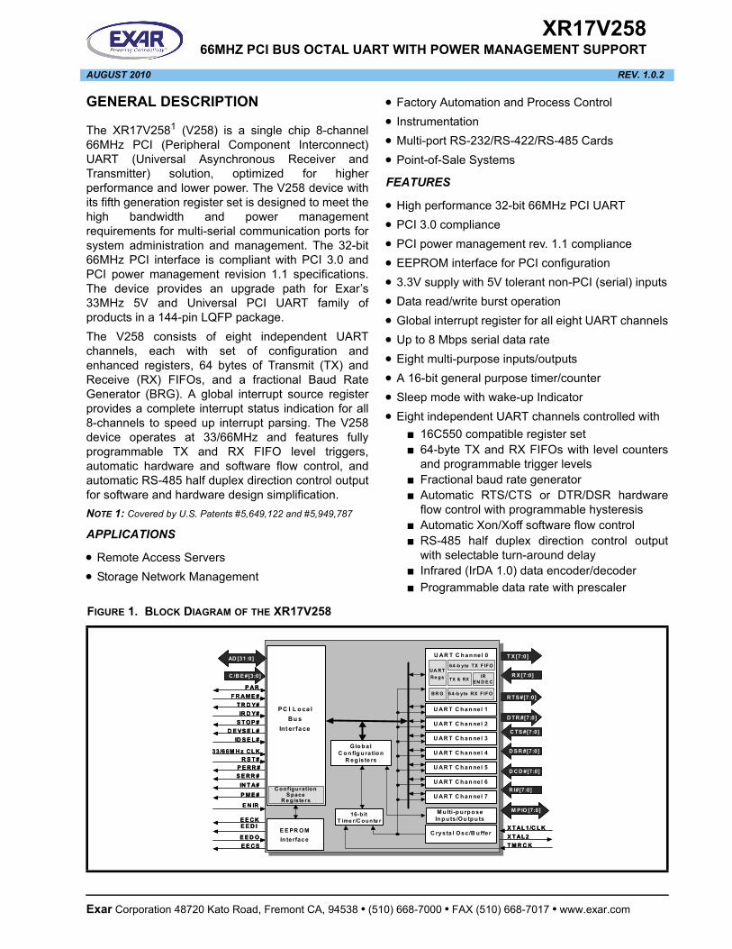
FIGURE 2. PIN OUT OF THE DEVICE
RX
4
GN
D
MPIO5
GND
TMRCK
ENIR
XR17V258
108
107
106
105
104
103
102
101
100
99 98 97 96 95 94 93 92 91 90 89 88 87 86 85 84 83 82 81 80 79
MPI
O0
MPI
O1
VCC
GN
D
CTS
4#
TX5
1 2 3 4 5 6 7 8 9 10 11 12 13 14 15 16 17 18 19 20 21 22 23 24 25 26 27 28 29 30
AD24
CB
E3
IDSE
L
GN
D
AD23
AD
22
AD21
AD
20
AD
19
AD18
AD17
AD
16
CBE
2
FRA
ME#
IRD
Y#
TRD
Y#
DEV
SEL#
STO
P#
PE
RR
#
SE
RR
#
PA
R
CB
E1
AD
15
AD14
AD13
AD12
AD11
TX7
RX6
CTS6#
DSR6#
CD6#
RI6#
RTS6#
DTR6#
TX6
GND
VCCMPIO7
MPIO6
MPIO4
RX5
CTS5#
53
54
55
56
57
58
59
60
61
62
63
64
65
66
67
68
69
70
71
72
RX1
CTS1#
DSR1#
CD1#
RI1#
RTS1#
DTR1#
TX1
EECS
EEDI
EECK
EEDO
VCC
PME#
XTAL1
XTAL2
128
127
126
125
124
123
122
121
120
119
118
117
116
115
114
113
112
111
110
109
31 32 33 34
AD10
AD9
AD8
35 36
GN
D
CBE
0
MP
IO2
78 77 76 75 74 73
DTR
5#
RTS
5#
RI5
#
CD
5#
MP
IO3
RI7#
DTR7#
AD7
AD6
AD5
AD4
AD3
AD2
AD1
AD0
RX7
CTS7#
DSR7#
CD7#
RTS7#
37
38
39
40
41
42
43
44
45
46
47
48
49
50
51
52
AD26
AD27
AD28
AD29
AD30
AD31
GND
CLK
RST#
144143
142
141
140
139
138
137
136
135
134
133
132
131
130
129
TX4
DTR
4#
RTS
4#
RI4
#
CD
4#
RX
3
CTS
3#
TX3
DTR
3#
RTS
3#
RI3
#
CD
3#
RX
2
CTS
2#
TX2
DTR
2#
RTS
2#
RI2
#
CD
2#
DS
R2#
DS
R3#
DSR
4#
DS
R5#
RX0
CTS0#
DSR0#
CD0#
RI0#
RTS0#
DTR0#
TX0
INTA#
AD25
VCC
VCC
VC
C
VCC
VC
C
ORDERING INFORMATION
PART NUMBER PACKAGE OPERATING TEMPERATURE RANGE DEVICE STATUS
XR17V258IV 144-Lead LQFP -40°C to +85°C Active
2
XR17V258REV. 1.0.2 66MHZ PCI BUS OCTAL UART WITH POWER MANAGEMENT SUPPORT
PIN DESCRIPTIONS
NAME PIN # TYPE DESCRIPTION
PCI LOCAL BUS INTERFACE
RST# 134 I PCI bus reset input (active LOW). It resets the PCI local bus configuration space registers, device configuration registers and UART channel registers to the default condition.
CLK 135 I PCI bus clock input of up to 66.67MHz.
AD31-AD25,AD24,
AD23-AD16, AD15-AD8, AD7-AD0
138-144, 1,
6-13,26-33,37-44
IO Address data lines [31:0] (bidirectional).
FRAME# 15 I Bus transaction cycle frame (active LOW). It indicates the beginning and duration of an access.
C/BE0#-C/BE3#
36,25,14,2 I Bus command/byte enable [3:0] (active LOW). This line is multiplexed for bus command during the address phase and byte enables during the data phase.
IRDY# 16 I Initiator ready (active LOW). During a write, it indicates that valid data is present on data bus. During a read, it indicates the master is ready to accept data.
TRDY# 17 O Target ready (active LOW).
STOP# 21 O Target request to stop current transaction (active LOW).
IDSEL 3 I Initialization device select (active HIGH).
DEVSEL# 18 O Device select to the XR17V258 (active LOW).
INTA# 133 OD Device interrupt from XR17V258 (open drain, active LOW).
PME# 111 OD Power Management Event signal. While in D3hot state, if the PME_Enable bit in the Power Management Control/Status Register is set, the V258 asserts the PME# upon receiving a new character or upon change of state of modem inputs on any channel.
PAR 24 IO Parity is even across AD[31:0] and C/BE[3:0]# (bidirectional, active HIGH).
PERR# 22 O Data parity error indicator, except for special cycle transactions (active LOW). Optional in bus target application.
SERR# 23 OD System error indicator, Address parity or data parity during special cycle transactions (open drain, active LOW). Optional in bus target application.
MODEM OR SERIAL I/O INTERFACE
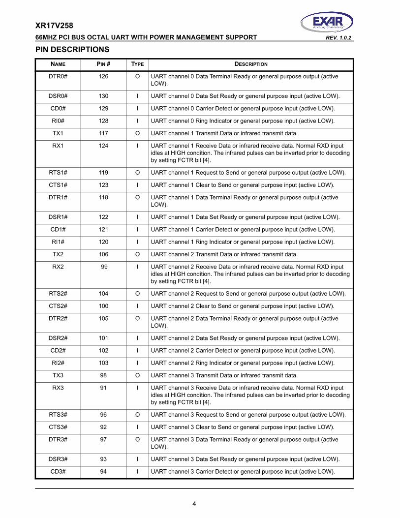
TX0 125 O UART channel 0 Transmit Data or infrared transmit data.
RX0 132 I UART channel 0 Receive Data or infrared receive data. Normal RXD input idles at HIGH condition. The infrared pulses can be inverted internally prior to decoding by setting FCTR bit [4].
RTS0# 127 O UART channel 0 Request to Send or general purpose output (active LOW).
CTS0# 131 I UART channel 0 Clear to Send or general purpose input (active LOW).
3
XR17V258 66MHZ PCI BUS OCTAL UART WITH POWER MANAGEMENT SUPPORT REV. 1.0.2
DTR0# 126 O UART channel 0 Data Terminal Ready or general purpose output (active LOW).
DSR0# 130 I UART channel 0 Data Set Ready or general purpose input (active LOW).
CD0# 129 I UART channel 0 Carrier Detect or general purpose input (active LOW).
RI0# 128 I UART channel 0 Ring Indicator or general purpose input (active LOW).
TX1 117 O UART channel 1 Transmit Data or infrared transmit data.
RX1 124 I UART channel 1 Receive Data or infrared receive data. Normal RXD input idles at HIGH condition. The infrared pulses can be inverted prior to decoding by setting FCTR bit [4].
RTS1# 119 O UART channel 1 Request to Send or general purpose output (active LOW).
CTS1# 123 I UART channel 1 Clear to Send or general purpose input (active LOW).
DTR1# 118 O UART channel 1 Data Terminal Ready or general purpose output (active LOW).
DSR1# 122 I UART channel 1 Data Set Ready or general purpose input (active LOW).
CD1# 121 I UART channel 1 Carrier Detect or general purpose input (active LOW).
RI1# 120 I UART channel 1 Ring Indicator or general purpose input (active LOW).
TX2 106 O UART channel 2 Transmit Data or infrared transmit data.
RX2 99 I UART channel 2 Receive Data or infrared receive data. Normal RXD input idles at HIGH condition. The infrared pulses can be inverted prior to decoding by setting FCTR bit [4].
RTS2# 104 O UART channel 2 Request to Send or general purpose output (active LOW).
CTS2# 100 I UART channel 2 Clear to Send or general purpose input (active LOW).
DTR2# 105 O UART channel 2 Data Terminal Ready or general purpose output (active LOW).
DSR2# 101 I UART channel 2 Data Set Ready or general purpose input (active LOW).
CD2# 102 I UART channel 2 Carrier Detect or general purpose input (active LOW).
RI2# 103 I UART channel 2 Ring Indicator or general purpose input (active LOW).
TX3 98 O UART channel 3 Transmit Data or infrared transmit data.
RX3 91 I UART channel 3 Receive Data or infrared receive data. Normal RXD input idles at HIGH condition. The infrared pulses can be inverted prior to decoding by setting FCTR bit [4].
RTS3# 96 O UART channel 3 Request to Send or general purpose output (active LOW).
CTS3# 92 I UART channel 3 Clear to Send or general purpose input (active LOW).
DTR3# 97 O UART channel 3 Data Terminal Ready or general purpose output (active LOW).
DSR3# 93 I UART channel 3 Data Set Ready or general purpose input (active LOW).
CD3# 94 I UART channel 3 Carrier Detect or general purpose input (active LOW).
PIN DESCRIPTIONS
NAME PIN # TYPE DESCRIPTION
4
XR17V258REV. 1.0.2 66MHZ PCI BUS OCTAL UART WITH POWER MANAGEMENT SUPPORT
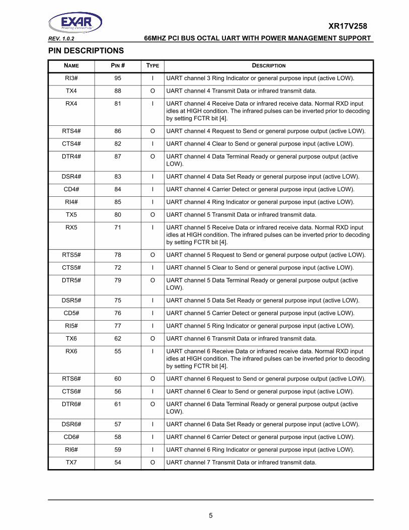
RI3# 95 I UART channel 3 Ring Indicator or general purpose input (active LOW).
TX4 88 O UART channel 4 Transmit Data or infrared transmit data.
RX4 81 I UART channel 4 Receive Data or infrared receive data. Normal RXD input idles at HIGH condition. The infrared pulses can be inverted prior to decoding by setting FCTR bit [4].
RTS4# 86 O UART channel 4 Request to Send or general purpose output (active LOW).
CTS4# 82 I UART channel 4 Clear to Send or general purpose input (active LOW).
DTR4# 87 O UART channel 4 Data Terminal Ready or general purpose output (active LOW).
DSR4# 83 I UART channel 4 Data Set Ready or general purpose input (active LOW).
CD4# 84 I UART channel 4 Carrier Detect or general purpose input (active LOW).
RI4# 85 I UART channel 4 Ring Indicator or general purpose input (active LOW).
TX5 80 O UART channel 5 Transmit Data or infrared transmit data.
RX5 71 I UART channel 5 Receive Data or infrared receive data. Normal RXD input idles at HIGH condition. The infrared pulses can be inverted prior to decoding by setting FCTR bit [4].
RTS5# 78 O UART channel 5 Request to Send or general purpose output (active LOW).
CTS5# 72 I UART channel 5 Clear to Send or general purpose input (active LOW).
DTR5# 79 O UART channel 5 Data Terminal Ready or general purpose output (active LOW).
DSR5# 75 I UART channel 5 Data Set Ready or general purpose input (active LOW).
CD5# 76 I UART channel 5 Carrier Detect or general purpose input (active LOW).
RI5# 77 I UART channel 5 Ring Indicator or general purpose input (active LOW).
TX6 62 O UART channel 6 Transmit Data or infrared transmit data.
RX6 55 I UART channel 6 Receive Data or infrared receive data. Normal RXD input idles at HIGH condition. The infrared pulses can be inverted prior to decoding by setting FCTR bit [4].
RTS6# 60 O UART channel 6 Request to Send or general purpose output (active LOW).
CTS6# 56 I UART channel 6 Clear to Send or general purpose input (active LOW).
DTR6# 61 O UART channel 6 Data Terminal Ready or general purpose output (active LOW).
DSR6# 57 I UART channel 6 Data Set Ready or general purpose input (active LOW).
CD6# 58 I UART channel 6 Carrier Detect or general purpose input (active LOW).
RI6# 59 I UART channel 6 Ring Indicator or general purpose input (active LOW).
TX7 54 O UART channel 7 Transmit Data or infrared transmit data.
PIN DESCRIPTIONS
NAME PIN # TYPE DESCRIPTION
5
XR17V258 66MHZ PCI BUS OCTAL UART WITH POWER MANAGEMENT SUPPORT REV. 1.0.2
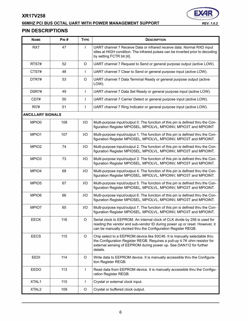
RX7 47 I UART channel 7 Receive Data or infrared receive data. Normal RXD input idles at HIGH condition. The infrared pulses can be inverted prior to decoding by setting FCTR bit [4].
RTS7# 52 O UART channel 7 Request to Send or general purpose output (active LOW).
CTS7# 48 I UART channel 7 Clear to Send or general purpose input (active LOW).
DTR7# 53 O UART channel 7 Data Terminal Ready or general purpose output (active LOW).
DSR7# 49 I UART channel 7 Data Set Ready or general purpose input (active LOW).
CD7# 50 I UART channel 7 Carrier Detect or general purpose input (active LOW).
RI7# 51 I UART channel 7 Ring Indicator or general purpose input (active LOW).
ANCILLARY SIGNALS
MPIO0 108 I/O Multi-purpose input/output 0. The function of this pin is defined thru the Con-figuration Register MPIOSEL, MPIOLVL, MPIOINV, MPIO3T and MPIOINT
MPIO1 107 I/O Multi-purpose input/output 1. The function of this pin is defined thru the Con-figuration Register MPIOSEL, MPIOLVL, MPIOINV, MPIO3T and MPIOINT.
MPIO2 74 I/O Multi-purpose input/output 2. The function of this pin is defined thru the Con-figuration Register MPIOSEL, MPIOLVL, MPIOINV, MPIO3T and MPIOINT.
MPIO3 73 I/O Multi-purpose input/output 3. The function of this pin is defined thru the Con-figuration Register MPIOSEL, MPIOLVL, MPIOINV, MPIO3T and MPIOINT.
MPIO4 68 I/O Multi-purpose input/output 4. The function of this pin is defined thru the Con-figuration Register MPIOSEL, MPIOLVL, MPIOINV, MPIO3T and MPIOINT.
MPIO5 67 I/O Multi-purpose input/output 5. The function of this pin is defined thru the Con-figuration Register MPIOSEL, MPIOLVL, MPIOINV, MPIO3T and MPIOINT.
MPIO6 66 I/O Multi-purpose input/output 6. The function of this pin is defined thru the Con-figuration Register MPIOSEL, MPIOLVL, MPIOINV, MPIO3T and MPIOINT.
MPIO7 65 I/O Multi-purpose input/output 7. The function of this pin is defined thru the Con-figuration Register MPIOSEL, MPIOLVL, MPIOINV, MPIO3T and MPIOINT.
EECK 116 O Serial clock to EEPROM. An internal clock of CLK divide by 256 is used for reading the vendor and sub-vendor ID during power up or reset. However, it can be manually clocked thru the Configuration Register REGB.
EECS 115 O Chip select to a EEPROM device like 93C46. It is manually selectable thru the Configuration Register REGB. Requires a pull-up 4.7K ohm resistor for external sensing of EEPROM during power up. See DAN112 for further details.
EEDI 114 O Write data to EEPROM device. It is manually accessible thru the Configura-tion Register REGB.
EEDO 113 I Read data from EEPROM device. It is manually accessible thru the Configu-ration Register REGB.
XTAL1 110 I Crystal or external clock input.
XTAL2 109 O Crystal or buffered clock output.
PIN DESCRIPTIONS
NAME PIN # TYPE DESCRIPTION
6
XR17V258REV. 1.0.2 66MHZ PCI BUS OCTAL UART WITH POWER MANAGEMENT SUPPORT
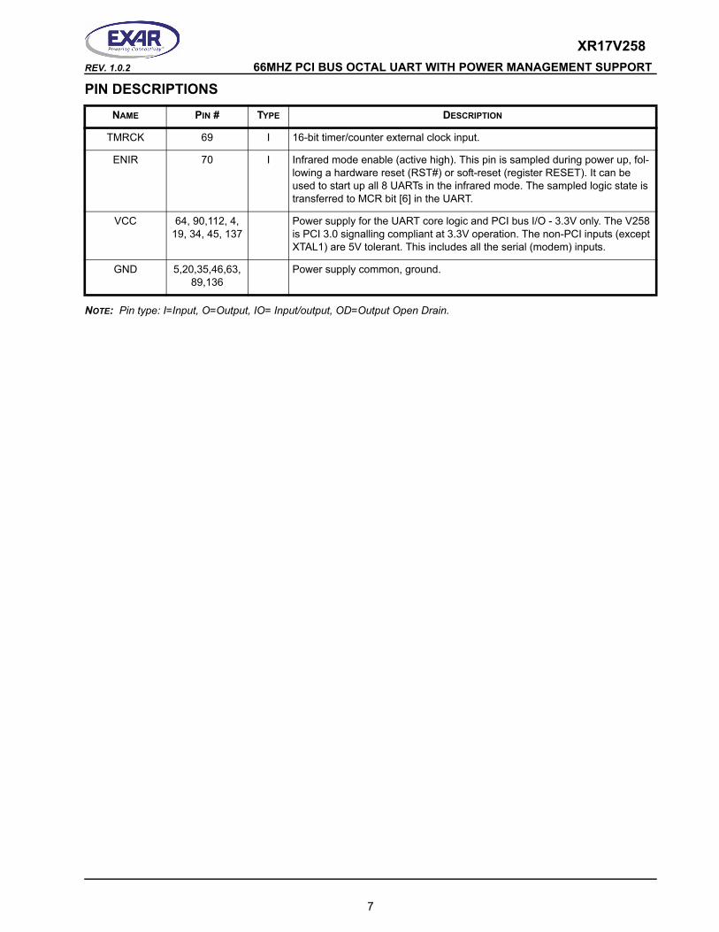
NOTE: Pin type: I=Input, O=Output, IO= Input/output, OD=Output Open Drain.
TMRCK 69 I 16-bit timer/counter external clock input.
ENIR 70 I Infrared mode enable (active high). This pin is sampled during power up, fol-lowing a hardware reset (RST#) or soft-reset (register RESET). It can be used to start up all 8 UARTs in the infrared mode. The sampled logic state is transferred to MCR bit [6] in the UART.
VCC 64, 90,112, 4, 19, 34, 45, 137
Power supply for the UART core logic and PCI bus I/O - 3.3V only. The V258 is PCI 3.0 signalling compliant at 3.3V operation. The non-PCI inputs (except XTAL1) are 5V tolerant. This includes all the serial (modem) inputs.
GND 5,20,35,46,63, 89,136
Power supply common, ground.
PIN DESCRIPTIONS
NAME PIN # TYPE DESCRIPTION
7
XR17V258 66MHZ PCI BUS OCTAL UART WITH POWER MANAGEMENT SUPPORT REV. 1.0.2
FUNCTIONAL DESCRIPTION The XR17V258 (V258) consists of eight enhanced 16550 UARTs with a conventional PCI interface and a non-volatile memory interface for PCI plug-and-play auto-configuration. The PCI local bus is a synchronous timing bus where all bus transactions are associated with the bus clock. The V258 supports 66MHz clock and 32-bit wide read and write data transfer operations including data burst mode through the PCI interface. Read and write data operations may be in byte, word or double-word (DWORD) format. The device consists of three sets of registers:
• PCI local bus configuration registers for PCI auto configuration• 32-bit global device configuration registers for overall control and monitoring of the 8 UART channels. • A combination set of the 16C550 compatible registers and enhanced registers in each of the individual UART
channel, for control, status, and byte wide data transferEach UART channel has 64-byte FIFOs, automatic RTS/CTS or DTR/DSR hardware flow control with hysteresis control, automatic Xon/Xoff software flow control, programmable transmit and receive FIFO trigger level, FIFO level counters, infrared encoder and decoder (IrDA ver. 1.0), and a programmable fractional baud rate generator with a prescaler of 1X or 4X, and data rate up to 8 Mbps at 8X sampling clock.The XR17V258 is available in a 144-pin LQFP (20x20x1.4mm) industrial grade package.PCI LOCAL BUS INTERFACE This is the host interface and it meets the PCI local bus specification revision 3.0. The PCI local bus operations are synchronous, where each transaction is associated to the bus clock. The V258 can operate with the bus clock of up to a 66.67MHz. Data transfers operation can be formatted in 8-bit, 16-bit, 24-bit or 32-bit wide. With 32-bit data operations, it pushes the data transfer rate on the bus up to 264 MByte/sec. This increases the overall system’s communication performance up to 32 times better than the 8-bit ISA bus. See PCI local bus specification revision 3.0 for bus operation details.PCI LOCAL BUS CONFIGURATION SPACE REGISTERS
A set of PCI local bus configuration space register is provided. These registers provide the PCI local bus operating system with the card’s vendor ID, device ID, sub-vendor ID, product model number, and resources and capabilities. The PCI local bus operating system collects this data from all the cards on the bus during the auto configuration phase that follows immediately after a power up or system reset/reboot. After it has sorted out all devices on the bus, it defines and download the operating conditions to the cards. One of the definitions is the base address loaded into the Base Address Register (BAR) where the card will be operating in the PCI local bus memory space. All this is described in more detail in “Section 1.1, PCI LOCAL BUS CONFIGURATION SPACE REGISTERS” on page 9.POWER MANAGEMENT REGISTERS
This set of registers is a continuation of the Configuration Space and provides status and control of Power Management functions of the V258. The Power Management Capabilities (PMC) register and the Power Management Control/Status Register (PMCSR) are implemented. “Section 1.2, Power Management Registers” on page 11 describes these registers and details how Power Management is implemented in the device.EEPROM INTERFACE An external 93C46 EEPROM is used to store 8 words of information. Details of this information can be found in “Section 1.4, EEPROM Interface” on page 14. This information is only used with the plug-and-play auto configuration of the PCI local bus. These data provide automatic hardware installation onto the PCI bus. The EEPROM interface consists of 4 signals, EEDI, EEDO, EECS, and EECK. The EEPROM is not needed when auto configuration is not required in the application. However, if your design requires non-volatile memory for other purpose, it is possible to store and retrieve data on the EEPROM through a special PCI device configuration register. See application note DAN112 for its programming details.
8
XR17V258REV. 1.0.2 66MHZ PCI BUS OCTAL UART WITH POWER MANAGEMENT SUPPORT
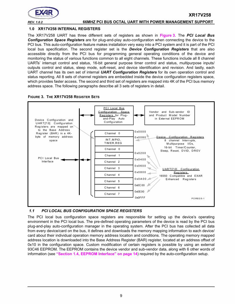
1.0 XR17V258 INTERNAL REGISTERSThe XR17V258 UART has three different sets of registers as shown in Figure 3. The PCI Local Bus Configuration Space Registers are for plug-and-play auto-configuration when connecting the device to the PCI bus. This auto-configuration feature makes installation very easy into a PCI system and it is part of the PCI local bus specification. The second register set is the Device Configuration Registers that are also accessible directly from the PCI bus for programming general operating conditions of the device and monitoring the status of various functions common to all eight channels. These functions include all 8 channel UARTs’ interrupt control and status, 16-bit general purpose timer control and status, multipurpose inputs/outputs control and status, sleep mode, soft-reset, and device identification and revision. And lastly, each UART channel has its own set of internal UART Configuration Registers for its own operation control and status reporting. All 8 sets of channel registers are embedded inside the device configuration registers space, which provides faster access. The second and third set of registers are mapped into 4K of the PCI bus memory address space. The following paragraphs describe all 3 sets of registers in detail.
FIGURE 3. THE XR17V258 REGISTER SETS
C hannel 0
IN T , M PIO,T IM ER , R EG
D evice C onfig uration andU AR T [7:0] C onfig uration
R eg isters are mapped onto the Base Address
R eg ister (BAR ) in a 4K-byte of memory address
space
PC I Local BusInter face
C hannel 0
C hannel 1
C hannel 2
C hannel 3
C hannel 4
C hannel 5
C hannel 6
C hannel 7
D evice C onfig uration R eg isters8 channel Inter rupts,
M ultipurpose I/Os,16-bit T imer /C ounter ,
Sleep, R eset, D VID , D R EV
U AR T[7:0] C onfig urationR eg isters
16550 C ompatible and EXAREnhanced R eg isters
PC I Local BusC onfig uration SpaceR eg isters for Plug -
and-Play AutoC onfig uration
PCIREG S-1
Vendor and Sub-vendor IDand Product M odel N umber
in External EEPR OM
0 x0 0 0 0
0 x0 2 0 0
0 x0 4 0 0
0 x0 6 0 0
0 x0 8 0 0
0 x0 A 0 0
0x0C 00
0x0E00
0 x0 0 8 0
0x0FF F
1.1 PCI LOCAL BUS CONFIGURATION SPACE REGISTERSThe PCI local bus configuration space registers are responsible for setting up the device’s operating environment in the PCI local bus. The pre-defined operating parameters of the device is read by the PCI bus plug-and-play auto-configuration manager in the operating system. After the PCI bus has collected all data from every device/card on the bus, it defines and downloads the memory mapping information to each device/card about their individual operation memory address location and conditions. The operating memory mapped address location is downloaded into the Base Address Register (BAR) register, located at an address offset of 0x10 in the configuration space. Custom modification of certain registers is possible by using an external 93C46 EEPROM. The EEPROM contains the device vendor and sub-vendor data, along with 6 other words of information (see “Section 1.4, EEPROM Interface” on page 14) required by the auto-configuration setup.
9
XR17V258 66MHZ PCI BUS OCTAL UART WITH POWER MANAGEMENT SUPPORT REV. 1.0.2
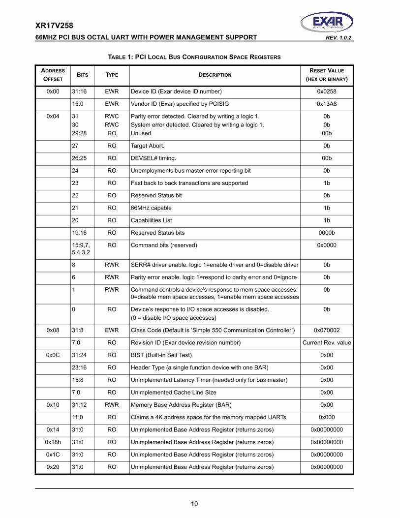
TABLE 1: PCI LOCAL BUS CONFIGURATION SPACE REGISTERS
ADDRESS
OFFSETBITS TYPE DESCRIPTION
RESET VALUE
(HEX OR BINARY)
0x00 31:16 EWR Device ID (Exar device ID number) 0x0258
15:0 EWR Vendor ID (Exar) specified by PCISIG 0x13A8
0x04 313029:28
RWCRWCRO
Parity error detected. Cleared by writing a logic 1.System error detected. Cleared by writing a logic 1.Unused
0b0b
00b
27 RO Target Abort. 0b
26:25 RO DEVSEL# timing. 00b
24 RO Unemployments bus master error reporting bit 0b
23 RO Fast back to back transactions are supported 1b
22 RO Reserved Status bit 0b
21 RO 66MHz capable 1b
20 RO Capabilities List 1b
19:16 RO Reserved Status bits 0000b
15:9,7, 5,4,3,2
RO Command bits (reserved) 0x0000
8 RWR SERR# driver enable. logic 1=enable driver and 0=disable driver 0b
6 RWR Parity error enable. logic 1=respond to parity error and 0=ignore 0b
1 RWR Command controls a device’s response to mem space accesses: 0=disable mem space accesses, 1=enable mem space accesses
0b
0 RO Device’s response to I/O space accesses is disabled.(0 = disable I/O space accesses)
0b
0x08 31:8 EWR Class Code (Default is ’Simple 550 Communication Controller’) 0x070002
7:0 RO Revision ID (Exar device revision number) Current Rev. value
0x0C 31:24 RO BIST (Built-in Self Test) 0x00
23:16 RO Header Type (a single function device with one BAR) 0x00
15:8 RO Unimplemented Latency Timer (needed only for bus master) 0x00
7:0 RO Unimplemented Cache Line Size 0x00
0x10 31:12 RWR Memory Base Address Register (BAR) 0x00
11:0 RO Claims a 4K address space for the memory mapped UARTs 0x000
0x14 31:0 RO Unimplemented Base Address Register (returns zeros) 0x00000000
0x18h 31:0 RO Unimplemented Base Address Register (returns zeros) 0x00000000
0x1C 31:0 RO Unimplemented Base Address Register (returns zeros) 0x00000000
0x20 31:0 RO Unimplemented Base Address Register (returns zeros) 0x00000000
10
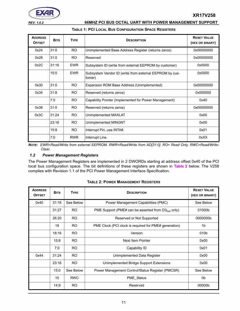
XR17V258REV. 1.0.2 66MHZ PCI BUS OCTAL UART WITH POWER MANAGEMENT SUPPORT
NOTE: EWR=Read/Write from external EEPROM. RWR=Read/Write from AD[31:0]. RO= Read Only. RWC=Read/Write-Clear.
1.2 Power Management RegistersThe Power Management Registers are implemented in 2 DWORDs starting at address offset 0x40 of the PCI local bus configuration space. The bit definitions of these registers are shown in Table 2 below. The V258 complies with Revision 1.1 of the PCI Power Management Interface Specification.
0x24 31:0 RO Unimplemented Base Address Register (returns zeros) 0x00000000
0x28 31:0 RO Reserved 0x00000000
0x2C 31:16 EWR Subsystem ID (write from external EEPROM by customer) 0x0000
15:0 EWR Subsystem Vendor ID (write from external EEPROM by cus-tomer)
0x0000
0x30 31:0 RO Expansion ROM Base Address (Unimplemented) 0x00000000
0x34 31:8 RO Reserved (returns zeros) 0x000000
7:0 RO Capability Pointer (Implemented for Power Management) 0x40
0x38 31:0 RO Reserved (returns zeros) 0x00000000
0x3C 31:24 RO Unimplemented MAXLAT 0x00
23:16 RO Unimplemented MINGNT 0x00
15:8 RO Interrupt Pin, use INTA#. 0x01
7:0 RWR Interrupt Line. 0xXX
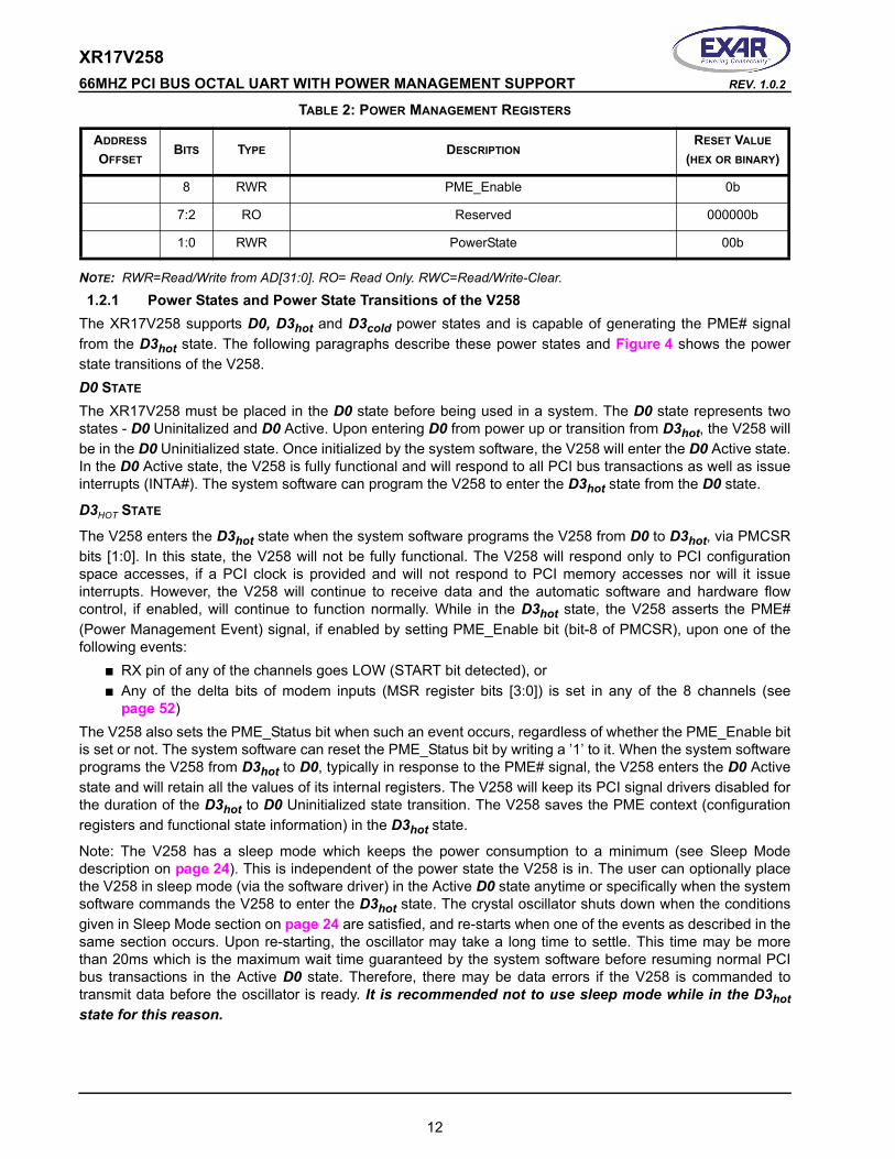
TABLE 2: POWER MANAGEMENT REGISTERS
ADDRESS
OFFSETBITS TYPE DESCRIPTION
RESET VALUE
(HEX OR BINARY)
0x40 31:16 See Below Power Management Capabilities (PMC) See Below
31:27 RO PME Support (PME# can be asserted from D3hot only) 01000b
26:20 RO Reserved or Not Supported 0000000b
19 RO PME Clock (PCI clock is required for PME# generation) 1b
18:16 RO Version 010b
15:8 RO Next Item Pointer 0x00
7:0 RO Capability ID 0x01
0x44 31:24 RO Unimplemented Data Register 0x00
23:16 RO Unimplemented Bridge Support Extensions 0x00
15:0 See Below Power Management Control/Status Register (PMCSR) See Below
15 RWC PME_Status 0b
14:9 RO Reserved 00000b
TABLE 1: PCI LOCAL BUS CONFIGURATION SPACE REGISTERS
ADDRESS
OFFSETBITS TYPE DESCRIPTION
RESET VALUE
(HEX OR BINARY)
11
XR17V258 66MHZ PCI BUS OCTAL UART WITH POWER MANAGEMENT SUPPORT REV. 1.0.2
NOTE: RWR=Read/Write from AD[31:0]. RO= Read Only. RWC=Read/Write-Clear.
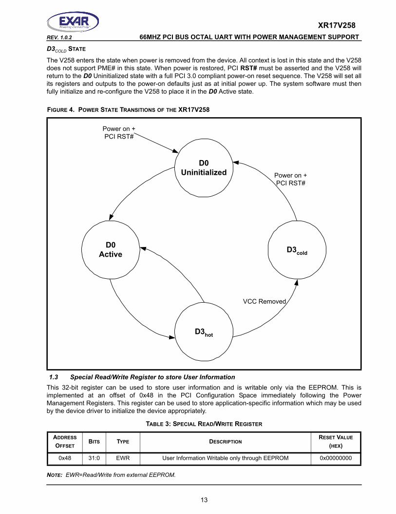
1.2.1 Power States and Power State Transitions of the V258The XR17V258 supports D0, D3hot and D3cold power states and is capable of generating the PME# signal from the D3hot state. The following paragraphs describe these power states and Figure 4 shows the power state transitions of the V258.D0 STATE
The XR17V258 must be placed in the D0 state before being used in a system. The D0 state represents two states - D0 Uninitalized and D0 Active. Upon entering D0 from power up or transition from D3hot, the V258 will be in the D0 Uninitialized state. Once initialized by the system software, the V258 will enter the D0 Active state. In the D0 Active state, the V258 is fully functional and will respond to all PCI bus transactions as well as issue interrupts (INTA#). The system software can program the V258 to enter the D3hot state from the D0 state.
D3HOT STATE
The V258 enters the D3hot state when the system software programs the V258 from D0 to D3hot, via PMCSR bits [1:0]. In this state, the V258 will not be fully functional. The V258 will respond only to PCI configuration space accesses, if a PCI clock is provided and will not respond to PCI memory accesses nor will it issue interrupts. However, the V258 will continue to receive data and the automatic software and hardware flow control, if enabled, will continue to function normally. While in the D3hot state, the V258 asserts the PME# (Power Management Event) signal, if enabled by setting PME_Enable bit (bit-8 of PMCSR), upon one of the following events:
■ RX pin of any of the channels goes LOW (START bit detected), or■ Any of the delta bits of modem inputs (MSR register bits [3:0]) is set in any of the 8 channels (see
page 52)The V258 also sets the PME_Status bit when such an event occurs, regardless of whether the PME_Enable bit is set or not. The system software can reset the PME_Status bit by writing a ’1’ to it. When the system software programs the V258 from D3hot to D0, typically in response to the PME# signal, the V258 enters the D0 Active state and will retain all the values of its internal registers. The V258 will keep its PCI signal drivers disabled for the duration of the D3hot to D0 Uninitialized state transition. The V258 saves the PME context (configuration registers and functional state information) in the D3hot state.
Note: The V258 has a sleep mode which keeps the power consumption to a minimum (see Sleep Mode description on page 24). This is independent of the power state the V258 is in. The user can optionally place the V258 in sleep mode (via the software driver) in the Active D0 state anytime or specifically when the system software commands the V258 to enter the D3hot state. The crystal oscillator shuts down when the conditions given in Sleep Mode section on page 24 are satisfied, and re-starts when one of the events as described in the same section occurs. Upon re-starting, the oscillator may take a long time to settle. This time may be more than 20ms which is the maximum wait time guaranteed by the system software before resuming normal PCI bus transactions in the Active D0 state. Therefore, there may be data errors if the V258 is commanded to transmit data before the oscillator is ready. It is recommended not to use sleep mode while in the D3hotstate for this reason.
8 RWR PME_Enable 0b
7:2 RO Reserved 000000b
1:0 RWR PowerState 00b
TABLE 2: POWER MANAGEMENT REGISTERS
ADDRESS
OFFSETBITS TYPE DESCRIPTION
RESET VALUE
(HEX OR BINARY)
12
XR17V258REV. 1.0.2 66MHZ PCI BUS OCTAL UART WITH POWER MANAGEMENT SUPPORT
D3COLD STATE
The V258 enters the state when power is removed from the device. All context is lost in this state and the V258 does not support PME# in this state. When power is restored, PCI RST# must be asserted and the V258 will return to the D0 Uninitialized state with a full PCI 3.0 compliant power-on reset sequence. The V258 will set all its registers and outputs to the power-on defaults just as at initial power up. The system software must then fully initialize and re-configure the V258 to place it in the D0 Active state.
FIGURE 4. POWER STATE TRANSITIONS OF THE XR17V258
D0Uninitialized
D3hot
D3coldD0
Active
Power on +PCI RST#
Power on +PCI RST#
VCC Removed
1.3 Special Read/Write Register to store User InformationThis 32-bit register can be used to store user information and is writable only via the EEPROM. This is implemented at an offset of 0x48 in the PCI Configuration Space immediately following the Power Management Registers. This register can be used to store application-specific information which may be used by the device driver to initialize the device appropriately.
TABLE 3: SPECIAL READ/WRITE REGISTER
ADDRESS
OFFSETBITS TYPE DESCRIPTION
RESET VALUE
(HEX)
0x48 31:0 EWR User Information Writable only through EEPROM 0x00000000
NOTE: EWR=Read/Write from external EEPROM.
13
XR17V258 66MHZ PCI BUS OCTAL UART WITH POWER MANAGEMENT SUPPORT REV. 1.0.2
1.4 EEPROM InterfaceThe V258 provides an interface to an Electrically Erasable Programmable Read Only Memory (EEPROM). The EEPROM must be a 93C46-like device, with its memory configured as 16-bit words. This interface is provided in order to program the registers in the PCI Configuration Space of the PCI UART during power-up. The following table gives the mapping of the EEPROM memory to the registers in the V258’s PCI Configuration Space. When the PCI RST# is negated, the V258 will download the data from the EEPROM, if it detects a HIGH on the EECS pin. The V258 takes a maximum of 216 PCI clocks from the rising edge of the PCI RST# signal to read the EEPROM data. For more details on the EEPROM interface, please refer to the application note DAN112 on Exar’s website.
TABLE 4: EEPROM ADDRESS DEFINITIONS
EEPROM MEMORY ADDRESS
EEPROM DATA [D15:D0]V258’S PCI CONFIGURATION
SPACE ADDRESS
(WORD OFFSET)DEFAULT VALUES
0x00 Vendor ID 0x00 0x13A8
0x01 Device ID 0x02 0x0258
0x02 Class Code* 0x08 0x0200
0x03 Class Code (Continued) 0x0A 0x0700
0x04 Subsystem Vendor ID 0x2C 0x0000
0x05 Subsystem ID 0x2E 0x0000
0x06 Special Register (Lower Word) 0x48 0x0000
0x07 Special Register (Upper Word) 0x4A 0x0000
NOTE: * Only the upper 8 bits in this word in EEPROM location are used and the lower 8 bits are ignored. The lower byte at PCI Config space 0x08 is Device Revision and is read-only.
1.5 Device Internal Register SetsThe Device Configuration Registers and the eight individual UART Configuration Registers of the V258 occupy 4K of PCI bus memory address space. These addresses are offset onto the basic memory address, a value loaded into the Memory Base Address Register (BAR) in the PCI local bus configuration register set. The UART Configuration Registers are mapped into 8 address blocks where each UART channel occupies 512 bytes memory space for its own registers that include the 16550 compatible registers. The Device Configuration Registers are embedded inside the UART channel zero’s address space between 0x0080 to 0x0093. All these registers can be accessed in 8, 16, 24 or 32 bits width depending on the starting address given by the host at the beginning of the bus cycle. Transmit and receive data may be loaded or unloaded in 8, 16, 24 or 32 bits format in special locations given in the Table 5 below. Every time a read or write operation is made to the transmit or receive register, its FIFO data pointer is automatically bumped to the next sequential data location either in byte, word or DWORD. One special case applies to the receive data unloading when reading the receive data together with its LSR register content. The host must read them in 16 or 32 bits format in order to maintain integrity of the data byte with its associated error flags. These special registers are further discussed in “Section 3.1, FIFO DATA LOADING AND UNLOADING IN 32-BIT FORMAT.” on page 28.
14
XR17V258REV. 1.0.2 66MHZ PCI BUS OCTAL UART WITH POWER MANAGEMENT SUPPORT
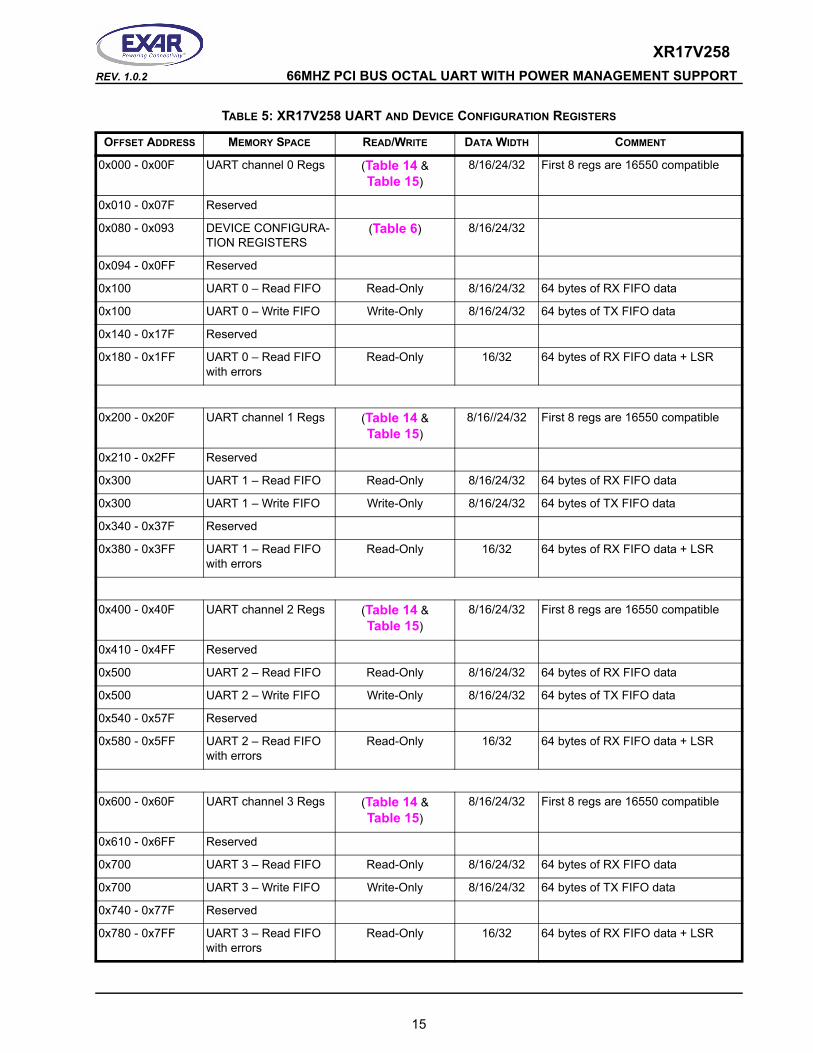
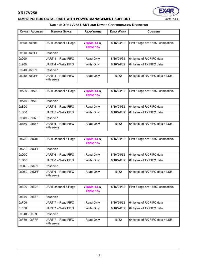
TABLE 5: XR17V258 UART AND DEVICE CONFIGURATION REGISTERS
OFFSET ADDRESS MEMORY SPACE READ/WRITE DATA WIDTH COMMENT
0x000 - 0x00F UART channel 0 Regs (Table 14 & Table 15)
8/16/24/32 First 8 regs are 16550 compatible
0x010 - 0x07F Reserved
0x080 - 0x093 DEVICE CONFIGURA-TION REGISTERS
(Table 6) 8/16/24/32
0x094 - 0x0FF Reserved
0x100 UART 0 – Read FIFO Read-Only 8/16/24/32 64 bytes of RX FIFO data
0x100 UART 0 – Write FIFO Write-Only 8/16/24/32 64 bytes of TX FIFO data
0x140 - 0x17F Reserved
0x180 - 0x1FF UART 0 – Read FIFO with errors
Read-Only 16/32 64 bytes of RX FIFO data + LSR
0x200 - 0x20F UART channel 1 Regs (Table 14 & Table 15)
8/16//24/32 First 8 regs are 16550 compatible
0x210 - 0x2FF Reserved
0x300 UART 1 – Read FIFO Read-Only 8/16/24/32 64 bytes of RX FIFO data
0x300 UART 1 – Write FIFO Write-Only 8/16/24/32 64 bytes of TX FIFO data
0x340 - 0x37F Reserved
0x380 - 0x3FF UART 1 – Read FIFO with errors
Read-Only 16/32 64 bytes of RX FIFO data + LSR
0x400 - 0x40F UART channel 2 Regs (Table 14 & Table 15)
8/16/24/32 First 8 regs are 16550 compatible
0x410 - 0x4FF Reserved
0x500 UART 2 – Read FIFO Read-Only 8/16/24/32 64 bytes of RX FIFO data
0x500 UART 2 – Write FIFO Write-Only 8/16/24/32 64 bytes of TX FIFO data
0x540 - 0x57F Reserved
0x580 - 0x5FF UART 2 – Read FIFO with errors
Read-Only 16/32 64 bytes of RX FIFO data + LSR
0x600 - 0x60F UART channel 3 Regs (Table 14 & Table 15)
8/16/24/32 First 8 regs are 16550 compatible
0x610 - 0x6FF Reserved
0x700 UART 3 – Read FIFO Read-Only 8/16/24/32 64 bytes of RX FIFO data
0x700 UART 3 – Write FIFO Write-Only 8/16/24/32 64 bytes of TX FIFO data
0x740 - 0x77F Reserved
0x780 - 0x7FF UART 3 – Read FIFO with errors
Read-Only 16/32 64 bytes of RX FIFO data + LSR
15
XR17V258 66MHZ PCI BUS OCTAL UART WITH POWER MANAGEMENT SUPPORT REV. 1.0.2
0x800 - 0x80F UART channel 4 Regs (Table 14 & Table 15)
8/16/24/32 First 8 regs are 16550 compatible
0x810 - 0x8FF Reserved
0x900 UART 4 – Read FIFO Read-Only 8/16/24/32 64 bytes of RX FIFO data
0x900 UART 4 – Write FIFO Write-Only 8/16/24/32 64 bytes of TX FIFO data
0x940 - 0x97F Reserved
0x980 - 0x9FF UART 4 – Read FIFO with errors
Read-Only 16/32 64 bytes of RX FIFO data + LSR
0xA00 - 0xA0F UART channel 5 Regs (Table 14 & Table 15)
8/16/24/32 First 8 regs are 16550 compatible
0xA10 - 0xAFF Reserved
0xB00 UART 5 – Read FIFO Read-Only 8/16/24/32 64 bytes of RX FIFO data
0xB00 UART 5 – Write FIFO Write-Only 8/16/24/32 64 bytes of TX FIFO data
0xB40 - 0xB7F Reserved
0xB80 - 0xBFF UART 5 – Read FIFO with errors
Read-Only 16/32 64 bytes of RX FIFO data + LSR
0xC00 - 0xC0F UART channel 6 Regs (Table 14 & Table 15)
8/16/24/32 First 8 regs are 16550 compatible
0xC10 - 0xCFF Reserved
0xD00 UART 6 – Read FIFO Read-Only 8/16/24/32 64 bytes of RX FIFO data
0xD00 UART 6 – Write FIFO Write-Only 8/16/24/32 64 bytes of TX FIFO data
0xD40 - 0xD7F Reserved
0xD80 - 0xDFF UART 6 – Read FIFO with errors
Read-Only 16/32 64 bytes of RX FIFO data + LSR
0xE00 - 0xE0F UART channel 7 Regs (Table 14 & Table 15)
8/16/24/32 First 8 regs are 16550 compatible
0xE10 - 0xEFF Reserved
0xF00 UART 7 – Read FIFO Read-Only 8/16/24/32 64 bytes of RX FIFO data
0xF00 UART 7 – Write FIFO Write-Only 8/16/24/32 64 bytes of TX FIFO data
0xF40 - 0xF7F Reserved
0xF80 - 0xFFF UART 7 – Read FIFO with errors
Read-Only 16/32 64 bytes of RX FIFO data + LSR
TABLE 5: XR17V258 UART AND DEVICE CONFIGURATION REGISTERS
OFFSET ADDRESS MEMORY SPACE READ/WRITE DATA WIDTH COMMENT
16
XR17V258REV. 1.0.2 66MHZ PCI BUS OCTAL UART WITH POWER MANAGEMENT SUPPORT
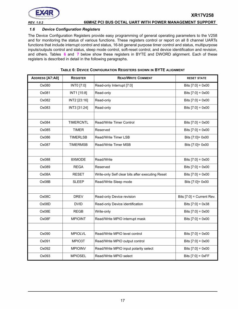
1.6 Device Configuration RegistersThe Device Configuration Registers provide easy programming of general operating parameters to the V258 and for monitoring the status of various functions. These registers control or report on all 8 channel UARTs functions that include interrupt control and status, 16-bit general purpose timer control and status, multipurpose inputs/outputs control and status, sleep mode control, soft-reset control, and device identification and revision, and others. Tables 6 and 7 below show these registers in BYTE and DWORD alignment. Each of these registers is described in detail in the following paragraphs.
TABLE 6: DEVICE CONFIGURATION REGISTERS SHOWN IN BYTE ALIGNMENT
ADDRESS [A7:A0] REGISTER READ/WRITE COMMENT RESET STATE
Ox080 INT0 [7:0] Read-only Interrupt [7:0] Bits [7:0] = 0x00
Ox081 INT1 [15:8] Read-only Bits [7:0] = 0x00
Ox082 INT2 [23:16] Read-only Bits [7:0] = 0x00
Ox083 INT3 [31:24] Read-only Bits [7:0] = 0x00
Ox084 TIMERCNTL Read/Write Timer Control Bits [7:0] = 0x00
Ox085 TIMER Reserved Bits [7:0] = 0x00
Ox086 TIMERLSB Read/Write Timer LSB Bits [7:0]= 0x00
Ox087 TIMERMSB Read/Write Timer MSB Bits [7:0]= 0x00
Ox088 8XMODE Read/Write Bits [7:0] = 0x00
Ox089 REGA Reserved Bits [7:0] = 0x00
Ox08A RESET Write-only Self clear bits after executing Reset Bits [7:0] = 0x00
Ox08B SLEEP Read/Write Sleep mode Bits [7:0]= 0x00
Ox08C DREV Read-only Device revision Bits [7:0] = Current Rev.
Ox08D DVID Read-only Device identification Bits [7:0] = 0x38
Ox08E REGB Write-only Bits [7:0] = 0x00
Ox08F MPIOINT Read/Write MPIO interrupt mask Bits [7:0] = 0x00
Ox090 MPIOLVL Read/Write MPIO level control Bits [7:0] = 0x00
Ox091 MPIO3T Read/Write MPIO output control Bits [7:0] = 0x00
Ox092 MPIOINV Read/Write MPIO input polarity select Bits [7:0] = 0x00
Ox093 MPIOSEL Read/Write MPIO select Bits [7:0] = 0xFF
17
XR17V258 66MHZ PCI BUS OCTAL UART WITH POWER MANAGEMENT SUPPORT REV. 1.0.2
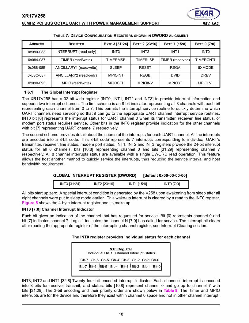
TABLE 7: DEVICE CONFIGURATION REGISTERS SHOWN IN DWORD ALIGNMENT
ADDRESS REGISTER BYTE 3 [31:24] BYTE 2 [23:16] BYTE 1 [15:8] BYTE 0 [7:0]
0x080-083 INTERRUPT (read-only) INT3 INT2 INT1 INT0
0x084-087 TIMER (read/write) TIMERMSB TIMERLSB TIMER (reserved) TIMERCNTL
0x088-08B ANCILLARY1 (read/write) SLEEP RESET REGA 8XMODE
0x08C-08F ANCILLARY2 (read-only) MPIOINT REGB DVID DREV
0x090-093 MPIO (read/write) MPIOSEL MPIOINV MPIO3T MPIOLVL
1.6.1 The Global Interrupt Register The XR17V258 has a 32-bit wide register [INT0, INT1, INT2 and INT3] to provide interrupt information and supports two interrupt schemes. The first scheme is an 8-bit indicator representing all 8 channels with each bit representing each channel from 0 to 7. This permits the interrupt service routine to quickly determine which UART channels need servicing so that it can go to the appropriate UART channel interrupt service routines. INT0 bit [0] represents the interrupt status for UART channel 0 when its transmitter, receiver, line status, or modem port status requires service. Other bits in the INT0 register provide indication for the other channels with bit [7] representing UART channel 7 respectively. The second scheme provides detail about the source of the interrupts for each UART channel. All the interrupts are encoded into a 3-bit code. This 3-bit code represents 7 interrupts corresponding to individual UART’s transmitter, receiver, line status, modem port status. INT1, INT2 and INT3 registers provide the 24-bit interrupt status for all 8 channels. bits [10:8] representing channel 0 and bits [31:29] representing channel 7 respectively. All 8 channel interrupts status are available with a single DWORD read operation. This feature allows the host another method to quickly service the interrupts, thus reducing the service interval and host bandwidth requirement.
GLOBAL INTERRUPT REGISTER (DWORD) [default 0x00-00-00-00]
INT3 [31:24] INT2 [23:16] INT1 [15:8] INT0 [7:0]
All bits start up zero. A special interrupt condition is generated by the V258 upon awakening from sleep after all eight channels were put to sleep mode earlier. This wake-up interrupt is cleared by a read to the INT0 register. Figure 5 shows the 4-byte interrupt register and its make up.INT0 [7:0] Channel Interrupt IndicatorEach bit gives an indication of the channel that has requested for service. Bit [0] represents channel 0 and bit [7] indicates channel 7. Logic 1 indicates the channel N [7:0] has called for service. The interrupt bit clears after reading the appropriate register of the interrupting channel register, see Interrupt Clearing section.
The INT0 register provides individual status for each channel
INT0 Register Individual UART Channel Interrupt Status
Ch-6Ch-7 Ch-5 Ch-4 Ch-3 Ch-2 Ch-1 Ch-0
Bit-7 Bit-6 Bit-5 Bit-4 Bit-3 Bit-2 Bit-1 Bit-0
INT3, INT2 and INT1 [32:8] Twenty four bit encoded interrupt indicator. Each channel’s interrupt is encoded into 3 bits for receive, transmit, and status. bits [10:8] represent channel 0 and go up to channel 7 with bits [31:29]. The 3-bit encoding and their priority order are shown below in Table 8. The Timer and MPIO interrupts are for the device and therefore they exist within channel 0 space and not in other channel interrupt.
18
XR17V258REV. 1.0.2 66MHZ PCI BUS OCTAL UART WITH POWER MANAGEMENT SUPPORT
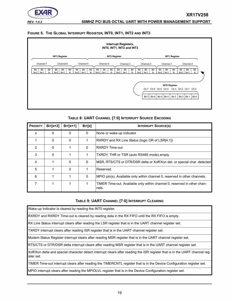
.FIGURE 5. THE GLOBAL INTERRUPT REGISTER, INT0, INT1, INT2 AND INT3
Channel-3 Channel-2 Channel-1 Channel-0
INT2 Register INT1 RegisterINT3 Register
INT0 Register
Interrupt Registers,INT0, INT1, INT2 and INT3
Bit-0Bit-1Bit-2Bit-3Bit-7 Bit-4Bit-5Bit-6
Ch-3 Ch-2 Ch-1 Ch-0
BitN+1
BitN+2
BitN
BitN+1
BitN+2
BitN
BitN+1
BitN+2
BitN
BitN+1
BitN+2
BitN
BitN+1
BitN+2
BitN
BitN+1
BitN+2
BitN
BitN+1
BitN+2
BitN
BitN+1
BitN+2
BitN
Ch-7 Ch-6 Ch-5 Ch-4
Channel-7 Channel-6 Channel-5 Channel-4
TABLE 8: UART CHANNEL [7:0] INTERRUPT SOURCE ENCODING
PRIORITY BIT[N+2] BIT[N+1] BIT[N] INTERRUPT SOURCE(S)
x 0 0 0 None or wake-up indicator
1 0 0 1 RXRDY and RX Line Status (logic OR of LSR[4:1])
2 0 1 0 RXRDY Time-out
3 0 1 1 TXRDY, THR or TSR (auto RS485 mode) empty
4 1 0 0 MSR, RTS/CTS or DTR/DSR delta or Xoff/Xon det. or special char. detected
5 1 0 1 Reserved.
6 1 1 0 MPIO pin(s). Available only within channel 0, reserved in other channels.
7 1 1 1 TIMER Time-out. Available only within channel 0, reserved in other chan-nels.
TABLE 9: UART CHANNEL [7:0] INTERRUPT CLEARING
Wake-up Indicator is cleared by reading the INT0 register.
RXRDY and RXRDY Time-out is cleared by reading data in the RX FIFO until the RX FIFO is empty.
RX Line Status interrupt clears after reading the LSR register that is in the UART channel register set.
TXRDY interrupt clears after reading ISR register that is in the UART channel register set.
Modem Status Register interrupt clears after reading MSR register that is in the UART channel register set.
RTS/CTS or DTR/DSR delta interrupt clears after reading MSR register that is in the UART channel register set.
Xoff/Xon delta and special character detect interrupt clears after reading the ISR register that is in the UART channel reg-ister set.
TIMER Time-out interrupt clears after reading the TIMERCNTL register that is in the Device Configuration register set.
MPIO interrupt clears after reading the MPIOLVL register that is in the Device Configuration register set.
19
XR17V258 66MHZ PCI BUS OCTAL UART WITH POWER MANAGEMENT SUPPORT REV. 1.0.2
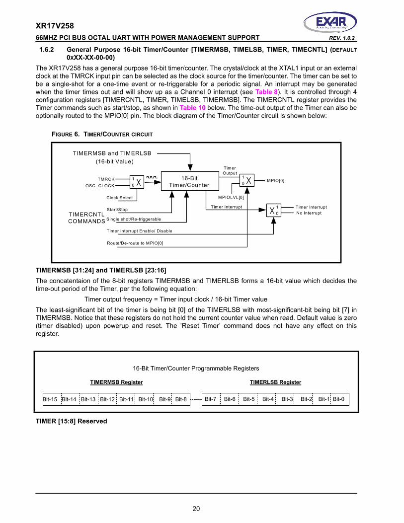
1.6.2 General Purpose 16-bit Timer/Counter [TIMERMSB, TIMELSB, TIMER, TIMECNTL] (DEFAULT 0XXX-XX-00-00)
The XR17V258 has a general purpose 16-bit timer/counter. The crystal/clock at the XTAL1 input or an external clock at the TMRCK input pin can be selected as the clock source for the timer/counter. The timer can be set to be a single-shot for a one-time event or re-triggerable for a periodic signal. An interrupt may be generated when the timer times out and will show up as a Channel 0 interrupt (see Table 8). It is controlled through 4 configuration registers [TIMERCNTL, TIMER, TIMELSB, TIMERMSB]. The TIMERCNTL register provides the Timer commands such as start/stop, as shown in Table 10 below. The time-out output of the Timer can also be optionally routed to the MPIO[0] pin. The block diagram of the Timer/Counter circuit is shown below:
FIGURE 6. TIMER/COUNTER CIRCUIT
Timer Interrupt
TimerOutput
MPIOLVL[0]
01
01 Timer Interrupt
No Interrupt
MPIO[0]TMRCKOSC. CLOCK
TIMERCNTLCOMMANDS
16-BitTimer/Counter
Start/Stop
Timer Interrupt Enable/ Disable
Single shot/Re-triggerable
TIMERMSB and TIMERLSB(16-bit Value)
01
Clock Select
Route/De-route to MPIO[0]
TIMERMSB [31:24] and TIMERLSB [23:16]The concatentaion of the 8-bit registers TIMERMSB and TIMERLSB forms a 16-bit value which decides the time-out period of the Timer, per the following equation:
Timer output frequency = Timer input clock / 16-bit Timer valueThe least-significant bit of the timer is being bit [0] of the TIMERLSB with most-significant-bit being bit [7] in TIMERMSB. Notice that these registers do not hold the current counter value when read. Default value is zero (timer disabled) upon powerup and reset. The ’Reset Timer’ command does not have any effect on this register.
TIMERMSB Register
Bit-15 Bit-14 Bit-13 Bit-12 Bit-11 Bit-10 Bit-9 Bit-8
TIMERLSB Register
Bit-7 Bit-6 Bit-5 Bit-4 Bit-3 Bit-2 Bit-1 Bit-0
16-Bit Timer/Counter Programmable Registers
TIMER [15:8] Reserved
20
XR17V258REV. 1.0.2 66MHZ PCI BUS OCTAL UART WITH POWER MANAGEMENT SUPPORT
TIMERCNTL [7:0] RegisterThe bits [3:0] of this register are used to issue commands. The commands are self-clearing, so reading this register does not show the last written command. Reading this register returns a value of 0x01 when the Timer interrupt is enabled and there is a pending Timer interrupt. It returns a value of 0x00 at all other times. The default settings of the Timer, upon power-up, a hardware reset or upon the issue of a ’Timer Reset’ command are:
■ Timer Interrupt Disabled■ Re-triggerable mode selected■ Internal crystal oscillator outputs selected as clock source■ Timer output not routed to MPIO[0]■ Timer stopped
TABLE 10: TIMER CONTROL REGISTERS
TIMERCNTL [7:4] Reserved
TIMERCNTL [3:0] These bits are used to invoke a series of commands that control the function of the Timer/Counter. The commands 1100 to 1111 are reserved.0001: Enable Timer Interrupt0010: Disable Timer Interrupt0011: Select One-shot mode0100: Select Re-triggerable mode0101: Select Internal Crystal Oscillator output as clock input for the Timer0110: Select External Clock input through the TMRCK pin for the Timer0111: Route Timer output to MPIO[0] pin1000: De-route Timer output from MPIO[0]1001: Start Timer1010: Stop Timer1011: Reset Timer
TIMER OPERATION
The following paragraphs describe the operation of the 16-bit Timer/Counter. The following conventions will be used in this discussion:
■ ’N’ is the 16-bit value programmed in the TIMER MSB, LSB registers■ P +Q = N, where ’P’ and ’Q’ are approximately half of ’N’.■ If N is even, P = Q = N/2.■ If N is odd, P = (N – 1)/2 and Q = (N + 1)/2.■ ‘N’ can take any value from 0x0002 to 0xFFFF.
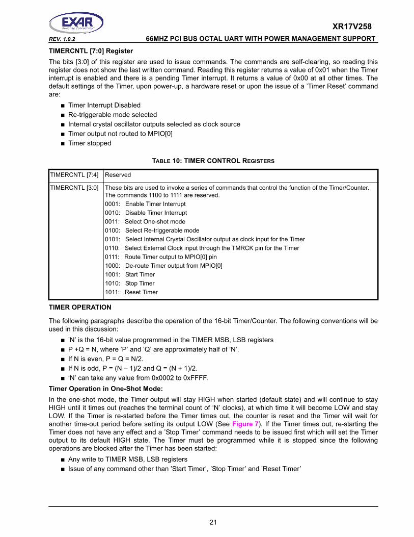
Timer Operation in One-Shot Mode:In the one-shot mode, the Timer output will stay HIGH when started (default state) and will continue to stay HIGH until it times out (reaches the terminal count of ‘N’ clocks), at which time it will become LOW and stay LOW. If the Timer is re-started before the Timer times out, the counter is reset and the Timer will wait for another time-out period before setting its output LOW (See Figure 7). If the Timer times out, re-starting the Timer does not have any effect and a ’Stop Timer’ command needs to be issued first which will set the Timer output to its default HIGH state. The Timer must be programmed while it is stopped since the following operations are blocked after the Timer has been started:
■ Any write to TIMER MSB, LSB registers■ Issue of any command other than ’Start Timer’, ’Stop Timer’ and ’Reset Timer’
21
XR17V258 66MHZ PCI BUS OCTAL UART WITH POWER MANAGEMENT SUPPORT REV. 1.0.2
Timer Operation in Re-triggerable Mode:In the re-triggerable mode, when the Timer is started, the Timer output will stay HIGH until it reaches half of the terminal count N (= P clocks) and toggle LOW and stay LOW for a similar amount of time (Q clocks). The above step will keep repeating until the Timer is stopped at which time the output will become HIGH (default state). See Figure 7. Also, after the Timer is started, re-starting the Timer does not have any effect in re-triggerable mode. The Timer must be programmed while it is stopped since the following operations are blocked when the Timer is running:
■ Any write to TIMER MSB, LSB registers■ Issue of any command other than ’Stop Timer’ and ’Reset Timer’ (’Start Timer’ is not allowed)
Routing the Timer Output to MPIO[0] Pin:MPIO[0] pin is by default (on power up or reset, for example) an input. However, whenever the Timer output is routed to MPIO[0] pin,
■ MPIO[0] will be automatically selected as an output■ MPIO[0] will become HIGH (the default state of Timer output)■ All MPIO control registers (MPIOLVL, MPIOSEL etc) lose control over MPIO[0] and get the control back
only when the Timer output is de-routed from MPIO[0].
FIGURE 7. TIMER OUTPUT IN ONE-SHOT AND RE-TRIGGERABLE MODES
TIMER Output inRe-triggerable
Mode
TIMER Output inOne-Shot Mode
After 'P'clocks
START TIMERCOMMAND ISSUED
START TIMERCOMMAND ISSUED
'N' Clocks
STOP TIMERCOMMAND ISSUED
START TIMER COMMANDS ISSUED: LESS THAN 'N'CLOCKS BETWEEN SUCCESSIVE COMMANDS
< 'N' Clocks
After 'P'clocks
After 'P'clocks
After 'P'clocks
After 'P'clocks
After 'Q'clocks
After 'Q'clocks
After 'Q'clocks
After 'Q'clocks
< 'N' Clocks
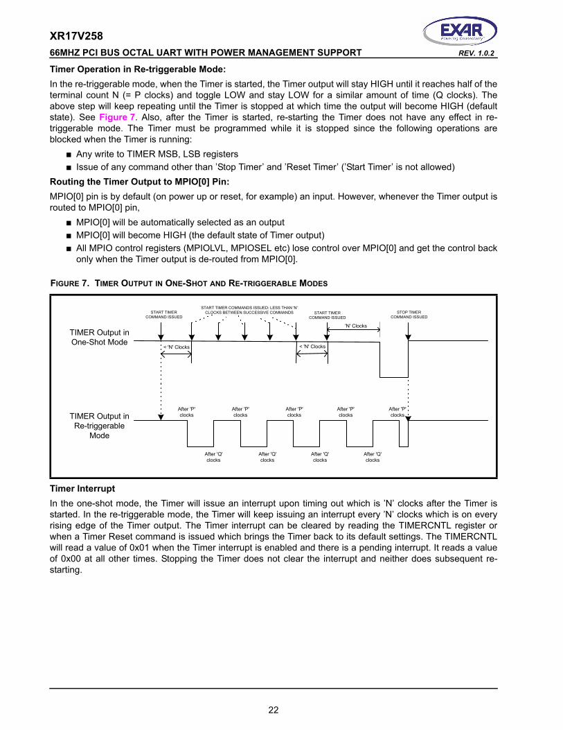
Timer InterruptIn the one-shot mode, the Timer will issue an interrupt upon timing out which is ’N’ clocks after the Timer is started. In the re-triggerable mode, the Timer will keep issuing an interrupt every ’N’ clocks which is on every rising edge of the Timer output. The Timer interrupt can be cleared by reading the TIMERCNTL register or when a Timer Reset command is issued which brings the Timer back to its default settings. The TIMERCNTL will read a value of 0x01 when the Timer interrupt is enabled and there is a pending interrupt. It reads a value of 0x00 at all other times. Stopping the Timer does not clear the interrupt and neither does subsequent re-starting.
22
XR17V258REV. 1.0.2 66MHZ PCI BUS OCTAL UART WITH POWER MANAGEMENT SUPPORT
FIGURE 8. INTERRUPT OUTPUT (ACTIVE LOW) IN ONE-SHOT AND RE-TRIGGERABLE MODES
One-shot Mode
Timer Started Timer Timed Out
TIMERCNTL read
Re-triggerable Mode
Timer Timed Out
TIMERCNTL read
Timer Timed Out
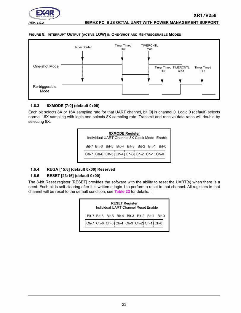
1.6.3 8XMODE [7:0] (default 0x00)Each bit selects 8X or 16X sampling rate for that UART channel, bit [0] is channel 0. Logic 0 (default) selects normal 16X sampling with logic one selects 8X sampling rate. Transmit and receive data rates will double by selecting 8X.
Ch-6Ch-7 Ch-5 Ch-4 Ch-3 Ch-2 Ch-1 Ch-0
8XMODE Register Individual UART Channel 8X Clock Mode Enable
Bit-7 Bit-6 Bit-5 Bit-4 Bit-3 Bit-2 Bit-1 Bit-0
1.6.4 REGA [15:8] (default 0x00) Reserved1.6.5 RESET [23:16] (default 0x00)
The 8-bit Reset register [RESET] provides the software with the ability to reset the UART(s) when there is a need. Each bit is self-clearing after it is written a logic 1 to perform a reset to that channel. All registers in that channel will be reset to the default condition, see Table 22 for details. .
Ch-6Ch-7 Ch-5 Ch-4 Ch-3 Ch-2 Ch-1 Ch-0
RESET Register Individual UART Channel Reset Enable
Bit-7 Bit-6 Bit-5 Bit-4 Bit-3 Bit-2 Bit-1 Bit-0
23
XR17V258 66MHZ PCI BUS OCTAL UART WITH POWER MANAGEMENT SUPPORT REV. 1.0.2
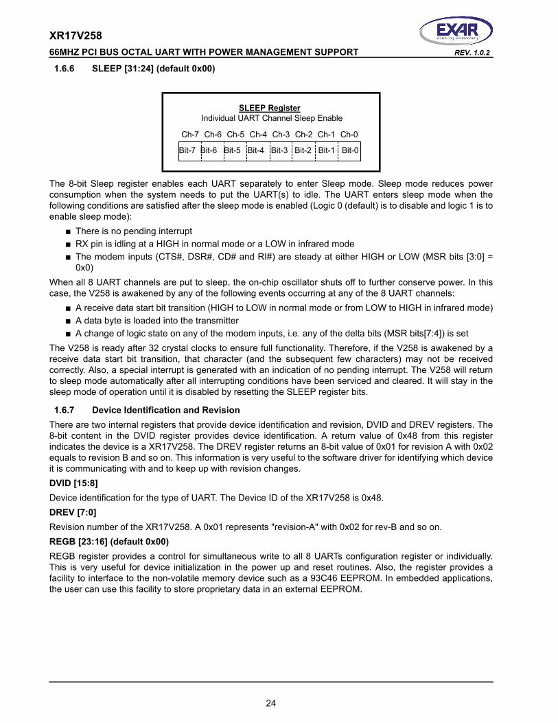
1.6.6 SLEEP [31:24] (default 0x00)
SLEEP Register Individual UART Channel Sleep Enable
Ch-6Ch-7 Ch-5 Ch-4 Ch-3 Ch-2 Ch-1 Ch-0
Bit-7 Bit-6 Bit-5 Bit-4 Bit-3 Bit-2 Bit-1 Bit-0
The 8-bit Sleep register enables each UART separately to enter Sleep mode. Sleep mode reduces power consumption when the system needs to put the UART(s) to idle. The UART enters sleep mode when the following conditions are satisfied after the sleep mode is enabled (Logic 0 (default) is to disable and logic 1 is to enable sleep mode):
■ There is no pending interrupt■ RX pin is idling at a HIGH in normal mode or a LOW in infrared mode■ The modem inputs (CTS#, DSR#, CD# and RI#) are steady at either HIGH or LOW (MSR bits [3:0] =
0x0)When all 8 UART channels are put to sleep, the on-chip oscillator shuts off to further conserve power. In this case, the V258 is awakened by any of the following events occurring at any of the 8 UART channels:
■ A receive data start bit transition (HIGH to LOW in normal mode or from LOW to HIGH in infrared mode)■ A data byte is loaded into the transmitter■ A change of logic state on any of the modem inputs, i.e. any of the delta bits (MSR bits[7:4]) is set
The V258 is ready after 32 crystal clocks to ensure full functionality. Therefore, if the V258 is awakened by a receive data start bit transition, that character (and the subsequent few characters) may not be received correctly. Also, a special interrupt is generated with an indication of no pending interrupt. The V258 will return to sleep mode automatically after all interrupting conditions have been serviced and cleared. It will stay in the sleep mode of operation until it is disabled by resetting the SLEEP register bits.
1.6.7 Device Identification and Revision There are two internal registers that provide device identification and revision, DVID and DREV registers. The 8-bit content in the DVID register provides device identification. A return value of 0x48 from this register indicates the device is a XR17V258. The DREV register returns an 8-bit value of 0x01 for revision A with 0x02 equals to revision B and so on. This information is very useful to the software driver for identifying which device it is communicating with and to keep up with revision changes.DVID [15:8] Device identification for the type of UART. The Device ID of the XR17V258 is 0x48.DREV [7:0] Revision number of the XR17V258. A 0x01 represents "revision-A" with 0x02 for rev-B and so on.REGB [23:16] (default 0x00)REGB register provides a control for simultaneous write to all 8 UARTs configuration register or individually. This is very useful for device initialization in the power up and reset routines. Also, the register provides a facility to interface to the non-volatile memory device such as a 93C46 EEPROM. In embedded applications, the user can use this facility to store proprietary data in an external EEPROM.
24
XR17V258REV. 1.0.2 66MHZ PCI BUS OCTAL UART WITH POWER MANAGEMENT SUPPORT
1.6.8 REGB Register
REGB[16](Read/Write) Logic 0 (default) write to each UART configuration registers individually.
Logic 1 enables simultaneous write to all 8 UARTs configuration register.
REGB[19:17] Reserved
REGB[20] (Write-Only) Control the EECK, clock, output (pin 116) on the EEPROM interface.
REGB[21] (Write-Only) Control the EECS, chips select, output (pin 115) to the EEPROM device.
REGB[22] (Write-Only) EEDI (pin 114) data input. Write data to the EEPROM device.
REGB[23] (Read-Only) EEDO (pin 113) data output. Read data from the EEPROM device.
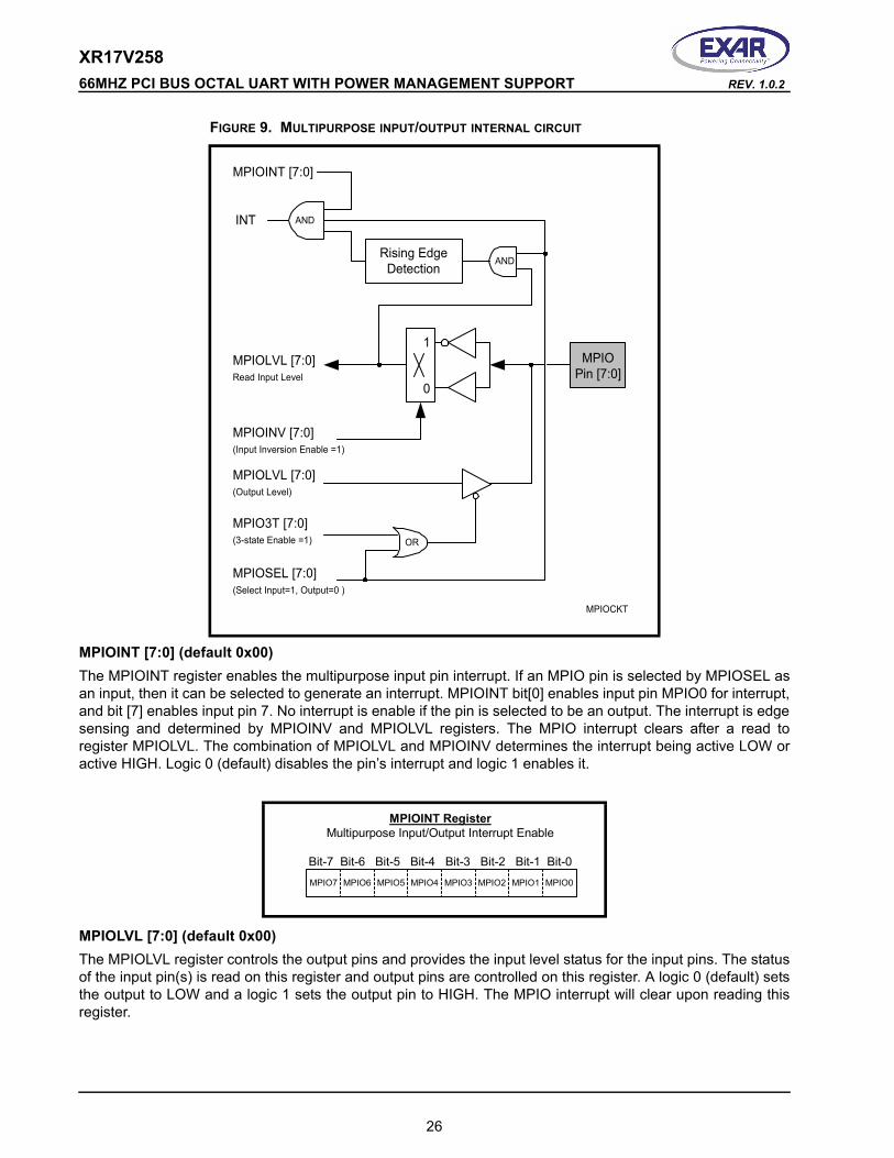
1.6.9 Multi-Purpose Inputs and Outputs The V258 provides 8 multi-purpose inputs/outputs MPIO[7:0] for general use. Each pin can be programmed to be an input or output function. The input logic state can be set for normal or inverted level, and optionally set to generate an interrupt. The outputs can be set to be normal HIGH or LOW state, or 3-state. Their functions and definitions are programmed through 5 registers: MPIOINT, MPIOLVL, MPIO3T, MPIOINV and MPIOSEL. If all 8 pins are set for inputs, all 8 interrupts would be ORed together. The ORed interrupt is reported in the channel 0 UART interrupt status, see Interrupt Status Register. The pins may also be programmed to be outputs and to the 3-state condition for signal sharing. The MPIO[0] pin can be programmed to show the Timer output. When it is programmed to be the Timer output, all the above 5 registers lose control over the MPIO[0] pin. For details on Timer output, please see “Section 1.6.2, General Purpose 16-bit Timer/Counter [TIMERMSB, TIMELSB, TIMER, TIMECNTL] (default 0xXX-XX-00-00)” on page 20.1.6.10 MPIO REGISTERS
There are 5 registers that select, control and monitor the 8 multipurpose inputs and outputs. Figure 9 shows the internal circuitry.
25
XR17V258 66MHZ PCI BUS OCTAL UART WITH POWER MANAGEMENT SUPPORT REV. 1.0.2
FIGURE 9. MULTIPURPOSE INPUT/OUTPUT INTERNAL CIRCUIT
MPIOPin [7:0]
MPIOLVL [7:0]Read Input Level
MPIOINT [7:0]
Rising EdgeDetection
INT
OR
AND
AND
1
0
MPIOSEL [7:0](Select Input=1, Output=0 )
MPIO3T [7:0](3-state Enable =1)
MPIOLVL [7:0](Output Level)
MPIOINV [7:0](Input Inversion Enable =1)
MPIOCKT
MPIOINT [7:0] (default 0x00)The MPIOINT register enables the multipurpose input pin interrupt. If an MPIO pin is selected by MPIOSEL as an input, then it can be selected to generate an interrupt. MPIOINT bit[0] enables input pin MPIO0 for interrupt, and bit [7] enables input pin 7. No interrupt is enable if the pin is selected to be an output. The interrupt is edge sensing and determined by MPIOINV and MPIOLVL registers. The MPIO interrupt clears after a read to register MPIOLVL. The combination of MPIOLVL and MPIOINV determines the interrupt being active LOW or active HIGH. Logic 0 (default) disables the pin’s interrupt and logic 1 enables it.
MPIO6MPIO7 MPIO5 MPIO4 MPIO3 MPIO2 MPIO1 MPIO0
MPIOINT RegisterMultipurpose Input/Output Interrupt Enable
Bit-7 Bit-6 Bit-5 Bit-4 Bit-3 Bit-2 Bit-1 Bit-0
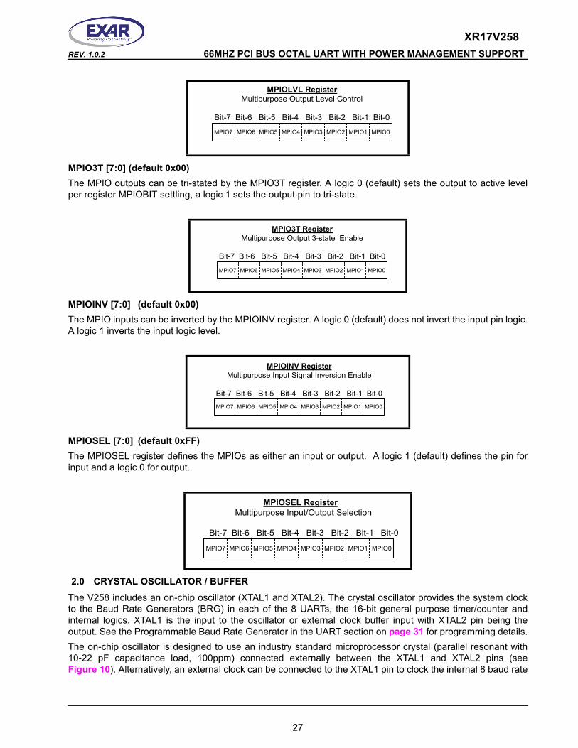
MPIOLVL [7:0] (default 0x00)The MPIOLVL register controls the output pins and provides the input level status for the input pins. The status of the input pin(s) is read on this register and output pins are controlled on this register. A logic 0 (default) sets the output to LOW and a logic 1 sets the output pin to HIGH. The MPIO interrupt will clear upon reading this register.
26
XR17V258REV. 1.0.2 66MHZ PCI BUS OCTAL UART WITH POWER MANAGEMENT SUPPORT
MPIO6MPIO7 MPIO5 MPIO4 MPIO3 MPIO2 MPIO1 MPIO0
MPIOLVL RegisterMultipurpose Output Level Control
Bit-7 Bit-6 Bit-5 Bit-4 Bit-3 Bit-2 Bit-1 Bit-0
MPIO3T [7:0] (default 0x00)The MPIO outputs can be tri-stated by the MPIO3T register. A logic 0 (default) sets the output to active level per register MPIOBIT settling, a logic 1 sets the output pin to tri-state.
MPIO6MPIO7 MPIO5 MPIO4 MPIO3 MPIO2 MPIO1 MPIO0
MPIO3T RegisterMultipurpose Output 3-state Enable
Bit-7 Bit-6 Bit-5 Bit-4 Bit-3 Bit-2 Bit-1 Bit-0
MPIOINV [7:0] (default 0x00)The MPIO inputs can be inverted by the MPIOINV register. A logic 0 (default) does not invert the input pin logic. A logic 1 inverts the input logic level.
MPIO6MPIO7 MPIO5 MPIO4 MPIO3 MPIO2 MPIO1 MPIO0
MPIOINV RegisterMultipurpose Input Signal Inversion Enable
Bit-7 Bit-6 Bit-5 Bit-4 Bit-3 Bit-2 Bit-1 Bit-0
MPIOSEL [7:0] (default 0xFF)The MPIOSEL register defines the MPIOs as either an input or output. A logic 1 (default) defines the pin for input and a logic 0 for output.
MPIO6MPIO7 MPIO5 MPIO4 MPIO3 MPIO2 MPIO1 MPIO0
MPIOSEL RegisterMultipurpose Input/Output Selection
Bit-7 Bit-6 Bit-5 Bit-4 Bit-3 Bit-2 Bit-1 Bit-0
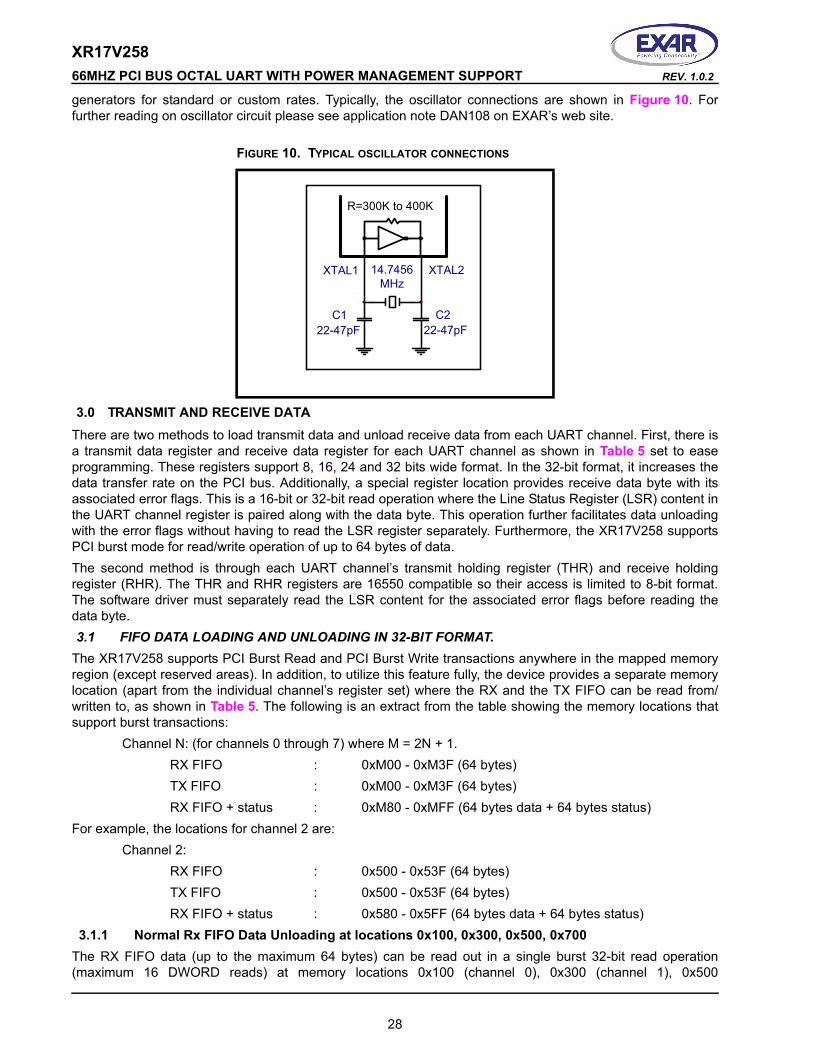
2.0 CRYSTAL OSCILLATOR / BUFFERThe V258 includes an on-chip oscillator (XTAL1 and XTAL2). The crystal oscillator provides the system clock to the Baud Rate Generators (BRG) in each of the 8 UARTs, the 16-bit general purpose timer/counter and internal logics. XTAL1 is the input to the oscillator or external clock buffer input with XTAL2 pin being the output. See the Programmable Baud Rate Generator in the UART section on page 31 for programming details.The on-chip oscillator is designed to use an industry standard microprocessor crystal (parallel resonant with 10-22 pF capacitance load, 100ppm) connected externally between the XTAL1 and XTAL2 pins (see Figure 10). Alternatively, an external clock can be connected to the XTAL1 pin to clock the internal 8 baud rate
27
XR17V258 66MHZ PCI BUS OCTAL UART WITH POWER MANAGEMENT SUPPORT REV. 1.0.2
generators for standard or custom rates. Typically, the oscillator connections are shown in Figure 10. For further reading on oscillator circuit please see application note DAN108 on EXAR’s web site.
FIGURE 10. TYPICAL OSCILLATOR CONNECTIONS
C122-47pF
C222-47pF
14.7456MHz
XTAL1 XTAL2
R=300K to 400K
3.0 TRANSMIT AND RECEIVE DATA There are two methods to load transmit data and unload receive data from each UART channel. First, there is a transmit data register and receive data register for each UART channel as shown in Table 5 set to ease programming. These registers support 8, 16, 24 and 32 bits wide format. In the 32-bit format, it increases the data transfer rate on the PCI bus. Additionally, a special register location provides receive data byte with its associated error flags. This is a 16-bit or 32-bit read operation where the Line Status Register (LSR) content in the UART channel register is paired along with the data byte. This operation further facilitates data unloading with the error flags without having to read the LSR register separately. Furthermore, the XR17V258 supports PCI burst mode for read/write operation of up to 64 bytes of data.The second method is through each UART channel’s transmit holding register (THR) and receive holding register (RHR). The THR and RHR registers are 16550 compatible so their access is limited to 8-bit format. The software driver must separately read the LSR content for the associated error flags before reading the data byte.3.1 FIFO DATA LOADING AND UNLOADING IN 32-BIT FORMAT.
The XR17V258 supports PCI Burst Read and PCI Burst Write transactions anywhere in the mapped memory region (except reserved areas). In addition, to utilize this feature fully, the device provides a separate memory location (apart from the individual channel’s register set) where the RX and the TX FIFO can be read from/written to, as shown in Table 5. The following is an extract from the table showing the memory locations that support burst transactions:
Channel N: (for channels 0 through 7) where M = 2N + 1.RX FIFO : 0xM00 - 0xM3F (64 bytes)TX FIFO : 0xM00 - 0xM3F (64 bytes)RX FIFO + status : 0xM80 - 0xMFF (64 bytes data + 64 bytes status)
For example, the locations for channel 2 are:Channel 2:
RX FIFO : 0x500 - 0x53F (64 bytes)TX FIFO : 0x500 - 0x53F (64 bytes)RX FIFO + status : 0x580 - 0x5FF (64 bytes data + 64 bytes status)
3.1.1 Normal Rx FIFO Data Unloading at locations 0x100, 0x300, 0x500, 0x700The RX FIFO data (up to the maximum 64 bytes) can be read out in a single burst 32-bit read operation (maximum 16 DWORD reads) at memory locations 0x100 (channel 0), 0x300 (channel 1), 0x500
28
XR17V258REV. 1.0.2 66MHZ PCI BUS OCTAL UART WITH POWER MANAGEMENT SUPPORT
(channel 2),......., 0xF00 (channel 7). This operation is at least 16 times faster than reading the data in 64 separate 8-bit memory reads of RHR register (0x000 for channel 0, 0x200 for channel 1, 0x400 for channel 2,......, 0xE00 for channel 7).
READ RX FIFO, WITH NO ERRORS
BYTE 3 BYTE 2 BYTE 1 BYTE 0
Read n+0 to n+3 FIFO Data n+3 FIFO Data n+2 FIFO Data n+1 FIFO Data n+0
Read n+4 to n+7 FIFO Data n+7 FIFO Data n+6 FIFO Data n+5 FIFO Data n+4
Etc.
PCI BusData Bit-31
B7 B6 B5 B4 B3 B2 B1 B0 B7 B6 B5 B4 B3 B2 B1 B0 B7 B6 B5 B4 B3 B2 B1 B0 B7 B6 B5 B4 B3 B2 B1 B0
Receive Data Byte n+3 Receive Data Byte n+2 Receive Data Byte n+1 Receive Data Byte n+0
PCI BusData Bit-0
Channel 0 to 7 ReceiveData in 32-bit alignment through the Configuration Register Address0x0100, 0x0300, 0x0500, 0x0700, 0x0900, 0x0B00, 0x0D00 and 0x0F00
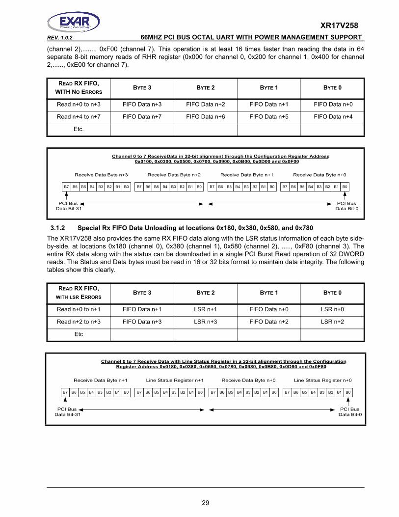
3.1.2 Special Rx FIFO Data Unloading at locations 0x180, 0x380, 0x580, and 0x780The XR17V258 also provides the same RX FIFO data along with the LSR status information of each byte side-by-side, at locations 0x180 (channel 0), 0x380 (channel 1), 0x580 (channel 2), ....., 0xF80 (channel 3). The entire RX data along with the status can be downloaded in a single PCI Burst Read operation of 32 DWORD reads. The Status and Data bytes must be read in 16 or 32 bits format to maintain data integrity. The following tables show this clearly.
READ RX FIFO, WITH LSR ERRORS
BYTE 3 BYTE 2 BYTE 1 BYTE 0
Read n+0 to n+1 FIFO Data n+1 LSR n+1 FIFO Data n+0 LSR n+0
Read n+2 to n+3 FIFO Data n+3 LSR n+3 FIFO Data n+2 LSR n+2
Etc
PCI BusData Bit-31
B7 B6 B5 B4 B3 B2 B1 B0 B7 B6 B5 B4 B3 B2 B1 B0 B7 B6 B5 B4 B3 B2 B1 B0 B7 B6 B5 B4 B3 B2 B1 B0
Receive Data Byte n+1 Line Status Register n+1 Receive Data Byte n+0 Line Status Register n+0
PCI BusData Bit-0
Channel 0 to 7 Receive Data with Line Status Register in a 32-bit alignment through the ConfigurationRegister Address 0x0180, 0x0380, 0x0580, 0x0780, 0x0980, 0x0B80, 0x0D80 and 0x0F80
29
XR17V258 66MHZ PCI BUS OCTAL UART WITH POWER MANAGEMENT SUPPORT REV. 1.0.2
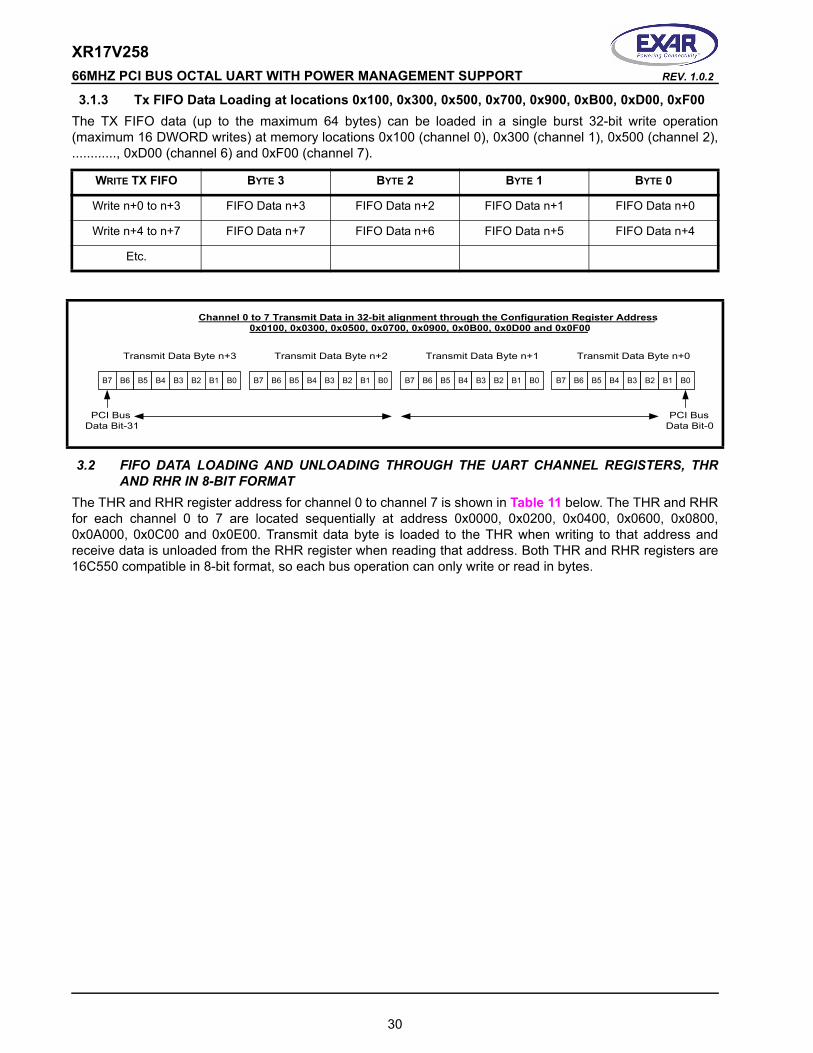
3.1.3 Tx FIFO Data Loading at locations 0x100, 0x300, 0x500, 0x700, 0x900, 0xB00, 0xD00, 0xF00The TX FIFO data (up to the maximum 64 bytes) can be loaded in a single burst 32-bit write operation (maximum 16 DWORD writes) at memory locations 0x100 (channel 0), 0x300 (channel 1), 0x500 (channel 2), ............, 0xD00 (channel 6) and 0xF00 (channel 7).
WRITE TX FIFO BYTE 3 BYTE 2 BYTE 1 BYTE 0
Write n+0 to n+3 FIFO Data n+3 FIFO Data n+2 FIFO Data n+1 FIFO Data n+0
Write n+4 to n+7 FIFO Data n+7 FIFO Data n+6 FIFO Data n+5 FIFO Data n+4
Etc.
PCI BusData Bit-31
B7 B6 B5 B4 B3 B2 B1 B0 B7 B6 B5 B4 B3 B2 B1 B0 B7 B6 B5 B4 B3 B2 B1 B0 B7 B6 B5 B4 B3 B2 B1 B0
Transmit Data Byte n+3 Transmit Data Byte n+2 Transmit Data Byte n+1 Transmit Data Byte n+0
PCI BusData Bit-0
Channel 0 to 7 Transmit Data in 32-bit alignment through the Configuration Register Address0x0100, 0x0300, 0x0500, 0x0700, 0x0900, 0x0B00, 0x0D00 and 0x0F00
3.2 FIFO DATA LOADING AND UNLOADING THROUGH THE UART CHANNEL REGISTERS, THR AND RHR IN 8-BIT FORMAT
The THR and RHR register address for channel 0 to channel 7 is shown in Table 11 below. The THR and RHR for each channel 0 to 7 are located sequentially at address 0x0000, 0x0200, 0x0400, 0x0600, 0x0800, 0x0A000, 0x0C00 and 0x0E00. Transmit data byte is loaded to the THR when writing to that address and receive data is unloaded from the RHR register when reading that address. Both THR and RHR registers are 16C550 compatible in 8-bit format, so each bus operation can only write or read in bytes.
30
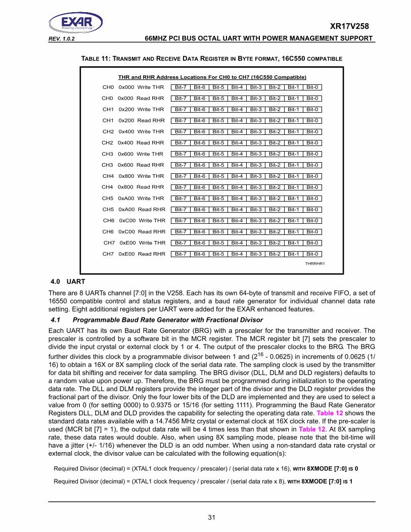
XR17V258REV. 1.0.2 66MHZ PCI BUS OCTAL UART WITH POWER MANAGEMENT SUPPORT
TABLE 11: TRANSMIT AND RECEIVE DATA REGISTER IN BYTE FORMAT, 16C550 COMPATIBLE
THR and RHR Address Locations For CH0 to CH7 (16C550 Compatible)
CH0 0x000 Write THR
CH0 0x000 Read RHR
CH1 0x200 Write THR
CH1 0x200 Read RHR
CH2 0x400 Write THR
CH2 0x400 Read RHR
CH3 0x600 Write THR
CH3 0x600 Read RHR
CH4 0x800 Write THR
CH4 0x800 Read RHR
CH5 0xA00 Write THR
CH5 0xA00 Read RHR
CH6 0xC00 Write THR
CH6 0xC00 Read RHR
CH7 0xE00 Write THR
CH7 0xE00 Read RHR
THRRHR1
Bit-7 Bit-6 Bit-5 Bit-4 Bit-3 Bit-2 Bit-1 Bit-0
Bit-7 Bit-6 Bit-5 Bit-4 Bit-3 Bit-2 Bit-1 Bit-0
Bit-7 Bit-6 Bit-5 Bit-4 Bit-3 Bit-2 Bit-1 Bit-0
Bit-7 Bit-6 Bit-5 Bit-4 Bit-3 Bit-2 Bit-1 Bit-0
Bit-7 Bit-6 Bit-5 Bit-4 Bit-3 Bit-2 Bit-1 Bit-0
Bit-7 Bit-6 Bit-5 Bit-4 Bit-3 Bit-2 Bit-1 Bit-0
Bit-7 Bit-6 Bit-5 Bit-4 Bit-3 Bit-2 Bit-1 Bit-0
Bit-7 Bit-6 Bit-5 Bit-4 Bit-3 Bit-2 Bit-1 Bit-0
Bit-7 Bit-6 Bit-5 Bit-4 Bit-3 Bit-2 Bit-1 Bit-0
Bit-7 Bit-6 Bit-5 Bit-4 Bit-3 Bit-2 Bit-1 Bit-0
Bit-7 Bit-6 Bit-5 Bit-4 Bit-3 Bit-2 Bit-1 Bit-0
Bit-7 Bit-6 Bit-5 Bit-4 Bit-3 Bit-2 Bit-1 Bit-0
Bit-7 Bit-6 Bit-5 Bit-4 Bit-3 Bit-2 Bit-1 Bit-0
Bit-7 Bit-6 Bit-5 Bit-4 Bit-3 Bit-2 Bit-1 Bit-0
Bit-7 Bit-6 Bit-5 Bit-4 Bit-3 Bit-2 Bit-1 Bit-0
Bit-7 Bit-6 Bit-5 Bit-4 Bit-3 Bit-2 Bit-1 Bit-0
4.0 UARTThere are 8 UARTs channel [7:0] in the V258. Each has its own 64-byte of transmit and receive FIFO, a set of 16550 compatible control and status registers, and a baud rate generator for individual channel data rate setting. Eight additional registers per UART were added for the EXAR enhanced features. 4.1 Programmable Baud Rate Generator with Fractional Divisor
Each UART has its own Baud Rate Generator (BRG) with a prescaler for the transmitter and receiver. The prescaler is controlled by a software bit in the MCR register. The MCR register bit [7] sets the prescaler to divide the input crystal or external clock by 1 or 4. The output of the prescaler clocks to the BRG. The BRG further divides this clock by a programmable divisor between 1 and (216 - 0.0625) in increments of 0.0625 (1/16) to obtain a 16X or 8X sampling clock of the serial data rate. The sampling clock is used by the transmitter for data bit shifting and receiver for data sampling. The BRG divisor (DLL, DLM and DLD registers) defaults to a random value upon power up. Therefore, the BRG must be programmed during initialization to the operating data rate. The DLL and DLM registers provide the integer part of the divisor and the DLD register provides the fractional part of the divisor. Only the four lower bits of the DLD are implemented and they are used to select a value from 0 (for setting 0000) to 0.9375 or 15/16 (for setting 1111). Programming the Baud Rate Generator Registers DLL, DLM and DLD provides the capability for selecting the operating data rate. Table 12 shows the standard data rates available with a 14.7456 MHz crystal or external clock at 16X clock rate. If the pre-scaler is used (MCR bit [7] = 1), the output data rate will be 4 times less than that shown in Table 12. At 8X sampling rate, these data rates would double. Also, when using 8X sampling mode, please note that the bit-time will have a jitter (+/- 1/16) whenever the DLD is an odd number. When using a non-standard data rate crystal or external clock, the divisor value can be calculated with the following equation(s):
Required Divisor (decimal) = (XTAL1 clock frequency / prescaler) / (serial data rate x 16), WITH 8XMODE [7:0] IS 0
Required Divisor (decimal) = (XTAL1 clock frequency / prescaler / (serial data rate x 8), WITH 8XMODE [7:0] IS 1
31
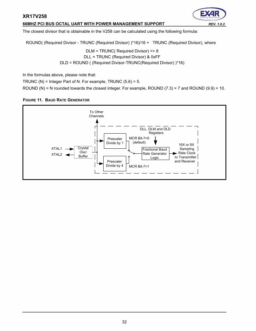
XR17V258 66MHZ PCI BUS OCTAL UART WITH POWER MANAGEMENT SUPPORT REV. 1.0.2
ROUND( (Required Divisor - TRUNC (Required Divisor) )*16)/16 + TRUNC (Required Divisor), where
DLM = TRUNC( Required Divisor) >> 8DLL = TRUNC (Required Divisor) & 0xFF
DLD = ROUND ( (Required Divisor-TRUNC(Required Divisor) )*16)
The closest divisor that is obtainable in the V258 can be calculated using the following formula:
In the formulas above, please note that:TRUNC (N) = Integer Part of N. For example, TRUNC (5.6) = 5.ROUND (N) = N rounded towards the closest integer. For example, ROUND (7.3) = 7 and ROUND (9.9) = 10.
FIGURE 11. BAUD RATE GENERATOR
XTAL1
XTAL2
CrystalOsc/
Buffer
MCR Bit-7=0(default)
MCR Bit-7=1
DLL, DLM and DLDRegisters
PrescalerDivide by 1
PrescalerDivide by 4
16X or 8XSampling
Rate Clockto Transmitterand Receiver
To OtherChannels
Fractional BaudRate Generator
Logic
32
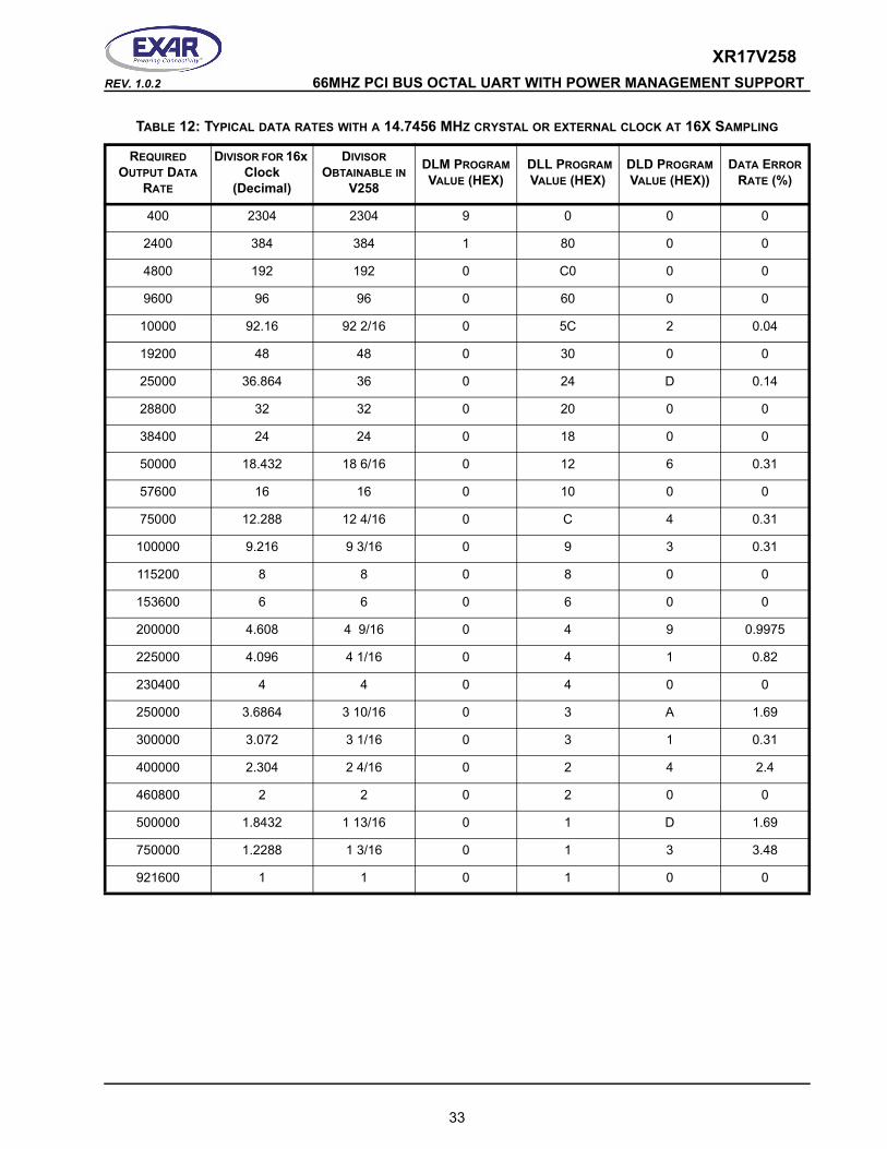
XR17V258REV. 1.0.2 66MHZ PCI BUS OCTAL UART WITH POWER MANAGEMENT SUPPORT
TABLE 12: TYPICAL DATA RATES WITH A 14.7456 MHZ CRYSTAL OR EXTERNAL CLOCK AT 16X SAMPLING
REQUIRED OUTPUT DATA
RATE
DIVISOR FOR 16x Clock
(Decimal)
DIVISOR OBTAINABLE IN
V258
DLM PROGRAM VALUE (HEX)
DLL PROGRAM VALUE (HEX)
DLD PROGRAM VALUE (HEX))
DATA ERROR RATE (%)
400 2304 2304 9 0 0 0
2400 384 384 1 80 0 0
4800 192 192 0 C0 0 0
9600 96 96 0 60 0 0
10000 92.16 92 2/16 0 5C 2 0.04
19200 48 48 0 30 0 0
25000 36.864 36 0 24 D 0.14
28800 32 32 0 20 0 0
38400 24 24 0 18 0 0
50000 18.432 18 6/16 0 12 6 0.31
57600 16 16 0 10 0 0
75000 12.288 12 4/16 0 C 4 0.31
100000 9.216 9 3/16 0 9 3 0.31
115200 8 8 0 8 0 0
153600 6 6 0 6 0 0
200000 4.608 4 9/16 0 4 9 0.9975
225000 4.096 4 1/16 0 4 1 0.82
230400 4 4 0 4 0 0
250000 3.6864 3 10/16 0 3 A 1.69
300000 3.072 3 1/16 0 3 1 0.31
400000 2.304 2 4/16 0 2 4 2.4
460800 2 2 0 2 0 0
500000 1.8432 1 13/16 0 1 D 1.69
750000 1.2288 1 3/16 0 1 3 3.48
921600 1 1 0 1 0 0
33
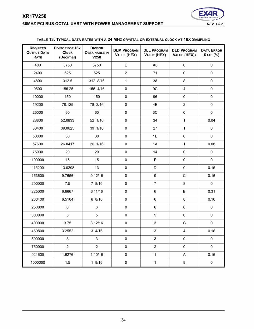
XR17V258 66MHZ PCI BUS OCTAL UART WITH POWER MANAGEMENT SUPPORT REV. 1.0.2
TABLE 13: TYPICAL DATA RATES WITH A 24 MHZ CRYSTAL OR EXTERNAL CLOCK AT 16X SAMPLING
REQUIRED OUTPUT DATA
RATE
DIVISOR FOR 16x Clock
(Decimal)
DIVISOR OBTAINABLE IN
V258
DLM PROGRAM VALUE (HEX)
DLL PROGRAM VALUE (HEX)
DLD PROGRAM VALUE (HEX))
DATA ERROR RATE (%)
400 3750 3750 E A6 0 0
2400 625 625 2 71 0 0
4800 312.5 312 8/16 1 38 8 0
9600 156.25 156 4/16 0 9C 4 0
10000 150 150 0 96 0 0
19200 78.125 78 2/16 0 4E 2 0
25000 60 60 0 3C 0 0
28800 52.0833 52 1/16 0 34 1 0.04
38400 39.0625 39 1/16 0 27 1 0
50000 30 30 0 1E 0 0
57600 26.0417 26 1/16 0 1A 1 0.08
75000 20 20 0 14 0 0
100000 15 15 0 F 0 0
115200 13.0208 13 0 D 0 0.16
153600 9.7656 9 12/16 0 9 C 0.16
200000 7.5 7 8/16 0 7 8 0
225000 6.6667 6 11/16 0 6 B 0.31
230400 6.5104 6 8/16 0 6 8 0.16
250000 6 6 0 6 0 0
300000 5 5 0 5 0 0
400000 3.75 3 12/16 0 3 C 0
460800 3.2552 3 4/16 0 3 4 0.16
500000 3 3 0 3 0 0
750000 2 2 0 2 0 0
921600 1.6276 1 10/16 0 1 A 0.16
1000000 1.5 1 8/16 0 1 8 0
34
XR17V258REV. 1.0.2 66MHZ PCI BUS OCTAL UART WITH POWER MANAGEMENT SUPPORT
4.2 Automatic Hardware (RTS/CTS or DTR/DSR) Flow Control OperationAutomatic hardware or RTS/DTR and CTS/DSR flow control is used to prevent data overrun to the local receiver FIFO and remote receiver FIFO. The RTS#/DTR# output pin is used to request remote unit to suspend/restart data transmission while the CTS#/DSR# input pin is monitored to suspend/restart local transmitter. The auto RTS/DTR and auto CTS/DSR flow control features are individually selected to fit specific application requirement and enabled through EFR bit[7:6] and MCR bit [2] for either RTS/CTS or DTR/DSR control signals. The auto RTS/DTR function must be started by asserting RTS/DTR# output pin (MCR bit [0] or bit [1] to logic 1) after it is enabled. Figure 12 below explains how it works.Two interrupts associated with RTS/DTR and CTS/DSR flow control have been added to give indication when RTS/DTR# pin or CTS/DSR# pin is de-asserted during operation. The RTS/DTR and CTS/DSR interrupts must be first enabled by EFR bit [4], and then enabled individually by IER bits [7:6], and chosen with MCR bit [2]. Automatic hardware flow control is selected by setting bits [7 (CTS): 6 (RTS)] of the EFR register to logic 1. If CTS# pin transitions from LOW to HIGH indicating a flow control request, ISR bit [5] will be set to logic 1, (if enabled via IER bit [7:6]), and the UART will suspend TX transmissions as soon as the stop bit of the character in process is shifted out. Transmission is resumed after the CTS# input returns to LOW, indicating more data may be sent.
35
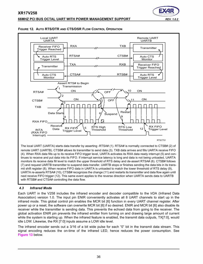
XR17V258 66MHZ PCI BUS OCTAL UART WITH POWER MANAGEMENT SUPPORT REV. 1.0.2
FIGURE 12. AUTO RTS/DTR AND CTS/DSR FLOW CONTROL OPERATION
RTSA# CTSB#
RXA TXBTransmitterReceiver FIFO
Trigger Reached
Auto RTSTrigger Level
Auto CTSMonitor
RTSA#
TXB
RXA FIFO
CTSB#
Remote UARTUARTB
Local UARTUARTA
ON OFF ON
SuspendRestart
RTS HighThreshold
Data Starts
ON OFF ON
Assert RTS# to BeginTransmission
1
2
3
4
5
6
7
ReceiveData
RTS LowThreshold
9
10
11
Receiver FIFOTrigger Reached
Auto RTSTrigger Level
Transmitter
Auto CTSMonitor
RTSB#CTSA#
RXBTXA
INTA(RXA FIFOInterrupt)
RX FIFOTrigger Level
RX FIFOTrigger Level
8
12
RTSCTS1
The local UART (UARTA) starts data transfer by asserting -RTSA# (1). RTSA# is normally connected to CTSB# (2) of remote UART (UARTB). CTSB# allows its transmitter to send data (3). TXB data arrives and fills UARTA receive FIFO (4). When RXA data fills up to its receive FIFO trigger level, UARTA activates its RXA data ready interrupt (5) and con-tinues to receive and put data into its FIFO. If interrupt service latency is long and data is not being unloaded, UARTA monitors its receive data fill level to match the upper threshold of RTS delay and de-assert RTSA# (6). CTSB# follows (7) and request UARTB transmitter to suspend data transfer. UARTB stops or finishes sending the data bits in its trans-mit shift register (8). When receive FIFO data in UARTA is unloaded to match the lower threshold of RTS delay (9), UARTA re-asserts RTSA# (10), CTSB# recognizes the change (11) and restarts its transmitter and data flow again until next receive FIFO trigger (12). This same event applies to the reverse direction when UARTA sends data to UARTB with RTSB# and CTSA# controlling the data flow.
4.3 Infrared Mode Each UART in the V258 includes the infrared encoder and decoder compatible to the IrDA (Infrared Data Association) version 1.0. The input pin ENIR conveniently activates all 8 UART channels to start up in the infrared mode. This global control pin enables the MCR bit [6] function in every UART channel register. After power up or a reset, the software can overwrite MCR bit [6] if so desired. ENIR and MCR bit [6] also disable its receiver while the transmitter is sending data. This prevents the echoed data from going to the receiver. The global activation ENIR pin prevents the infrared emitter from turning on and drawing large amount of current while the system is starting up. When the infrared feature is enabled, the transmit data outputs, TX[7:0], would idle LOW. Likewise, the RX [7:0] inputs assume a LOW idle level. The infrared encoder sends out a 3/16 of a bit wide pulse for each “0” bit in the transmit data stream. This signal encoding reduces the on-time of the infrared LED, hence reduces the power consumption. SeeFigure 13 below.
36
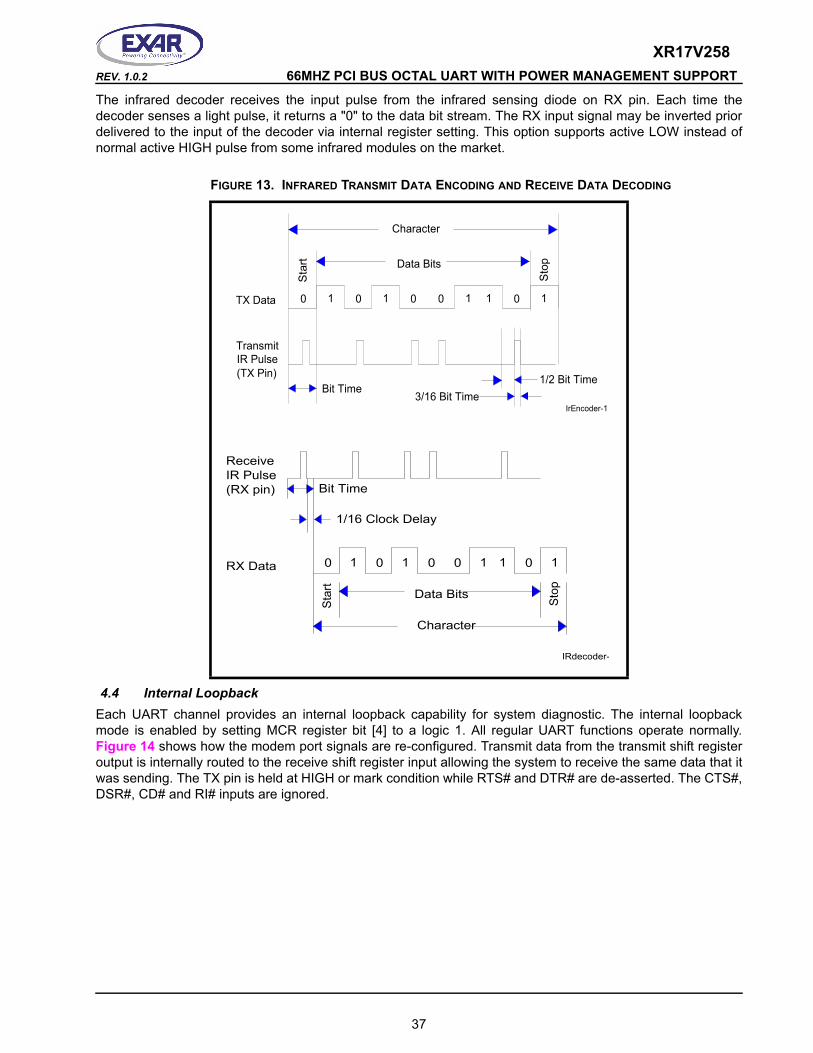
XR17V258REV. 1.0.2 66MHZ PCI BUS OCTAL UART WITH POWER MANAGEMENT SUPPORT
The infrared decoder receives the input pulse from the infrared sensing diode on RX pin. Each time the decoder senses a light pulse, it returns a "0" to the data bit stream. The RX input signal may be inverted prior delivered to the input of the decoder via internal register setting. This option supports active LOW instead of normal active HIGH pulse from some infrared modules on the market.
FIGURE 13. INFRARED TRANSMIT DATA ENCODING AND RECEIVE DATA DECODING
Character
Data Bits
Sta
rt
Sto
p0 0 0 0 01 1 1 1 1
Bit Time
1/16 Clock Delay
IRdecoder-
RX Data
ReceiveIR Pulse(RX pin)
Character
Data Bits
Sta
rt
Sto
p
0 0 0 0 01 1 1 1 1TX Data
TransmitIR Pulse(TX Pin)
Bit Time1/2 Bit Time
3/16 Bit TimeIrEncoder-1
4.4 Internal LoopbackEach UART channel provides an internal loopback capability for system diagnostic. The internal loopback mode is enabled by setting MCR register bit [4] to a logic 1. All regular UART functions operate normally. Figure 14 shows how the modem port signals are re-configured. Transmit data from the transmit shift register output is internally routed to the receive shift register input allowing the system to receive the same data that it was sending. The TX pin is held at HIGH or mark condition while RTS# and DTR# are de-asserted. The CTS#, DSR#, CD# and RI# inputs are ignored.
37
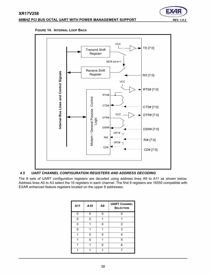
XR17V258 66MHZ PCI BUS OCTAL UART WITH POWER MANAGEMENT SUPPORT REV. 1.0.2
FIGURE 14. INTERNAL LOOP BACK
TX [7:0]
RX [7:0]
Mod
em /
Gen
eral
Pur
pose
Con
trol
Logi
c
Inte
rnal
Bus
Lin
es a
nd C
ontr
ol S
igna
ls
RTS# [7:0]
MCR bit-4=1
VCC
VCC
VCC
Transmit ShiftRegister
Receive ShiftRegister
CTS# [7:0]
DTR# [7:0]
DSR# [7:0]
RI# [7:0]
CD# [7:0]
OP1#
OP2#
RTS#
CTS#
DTR#
DSR#
RI#
CD#
4.5 UART CHANNEL CONFIGURATION REGISTERS AND ADDRESS DECODING The 8 sets of UART configuration registers are decoded using address lines A9 to A11 as shown below. Address lines A0 to A3 select the 16 registers in each channel. The first 8 registers are 16550 compatible with EXAR enhanced feature registers located on the upper 8 addresses.
CHANNEL SELECTION
0 0 0 0
0 0 1 1
0 1 0 2
0 1 1 3
1 0 0 4
1 0 1 5
1 1 0 6
1 1 1 7
A11 A10 A9 UART
38
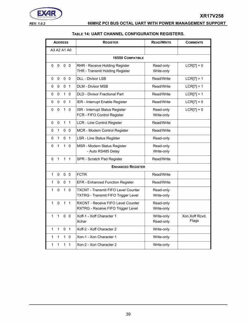
XR17V258REV. 1.0.2 66MHZ PCI BUS OCTAL UART WITH POWER MANAGEMENT SUPPORT
TABLE 14: UART CHANNEL CONFIGURATION REGISTERS.
ADDRESS REGISTER READ/WRITE COMMENTS
A3 A2 A1 A0
16550 COMPATIBLE
0 0 0 0 RHR - Receive Holding RegisterTHR - Transmit Holding Register
Read-onlyWrite-only
LCR[7] = 0
0 0 0 0 DLL - Divisor LSB Read/Write LCR[7] = 1
0 0 0 1 DLM - Divisor MSB Read/Write LCR[7] = 1
0 0 1 0 DLD - Divisor Fractional Part Read/Write LCR[7] = 1
0 0 0 1 IER - Interrupt Enable Register Read/Write LCR[7] = 0
0 0 1 0 ISR - Interrupt Status RegisterFCR - FIFO Control Register
Read-onlyWrite-only
LCR[7] = 0
0 0 1 1 LCR - Line Control Register Read/Write
0 1 0 0 MCR - Modem Control Register Read/Write
0 1 0 1 LSR - Line Status Register Read-only
0 1 1 0 MSR - Modem Status Register - Auto RS485 Delay
Read-onlyWrite-only
0 1 1 1 SPR - Scratch Pad Register Read/Write
ENHANCED REGISTER
1 0 0 0 FCTR Read/Write
1 0 0 1 EFR - Enhanced Function Register Read/Write
1 0 1 0 TXCNT - Transmit FIFO Level CounterTXTRG - Transmit FIFO Trigger Level
Read-onlyWrite-only
1 0 1 1 RXCNT - Receive FIFO Level CounterRXTRG - Receive FIFO Trigger Level
Read-onlyWrite-only
1 1 0 0 Xoff-1 - Xoff Character 1Xchar
Write-onlyRead-only
Xon,Xoff Rcvd. Flags
1 1 0 1 Xoff-2 - Xoff Character 2 Write-only
1 1 1 0 Xon-1 - Xon Character 1 Write-only
1 1 1 1 Xon-2 - Xon Character 2 Write-only
39
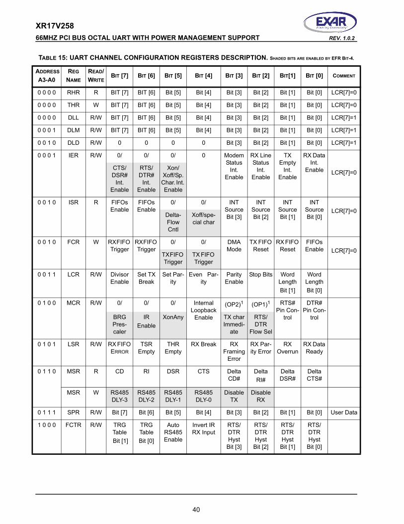
XR17V258 66MHZ PCI BUS OCTAL UART WITH POWER MANAGEMENT SUPPORT REV. 1.0.2
40
TABLE 15: UART CHANNEL CONFIGURATION REGISTERS DESCRIPTION. SHADED BITS ARE ENABLED BY EFR BIT-4.
ADDRESS
A3-A0REG
NAME
READ/WRITE
BIT [7] BIT [6] BIT [5] BIT [4] BIT [3] BIT [2] BIT[1] BIT [0] COMMENT
0 0 0 0 RHR R BIT [7] BIT [6] Bit [5] Bit [4] Bit [3] Bit [2] Bit [1] Bit [0] LCR[7]=0
0 0 0 0 THR W BIT [7] BIT [6] Bit [5] Bit [4] Bit [3] Bit [2] Bit [1] Bit [0] LCR[7]=0
0 0 0 0 DLL R/W BIT [7] BIT [6] Bit [5] Bit [4] Bit [3] Bit [2] Bit [1] Bit [0] LCR[7]=1
0 0 0 1 DLM R/W BIT [7] BIT [6] Bit [5] Bit [4] Bit [3] Bit [2] Bit [1] Bit [0] LCR[7]=1
0 0 1 0 DLD R/W 0 0 0 0 Bit [3] Bit [2] Bit [1] Bit [0] LCR[7]=1
0 0 0 1 IER R/W 0/ 0/ 0/ 0 Modem Status
Int. Enable
RX Line Status
Int. Enable
TX Empty
Int. Enable
RX Data Int.
Enable LCR[7]=0CTS/DSR#
Int. Enable
RTS/DTR#
Int. Enable
Xon/Xoff/Sp.
Char. Int. Enable
0 0 1 0 ISR R FIFOs Enable
FIFOs Enable
0/ 0/ INT Source Bit [3]
INT Source Bit [2]
INT Source Bit [1]
INT Source Bit [0]
LCR[7]=0Delta-Flow Cntl
Xoff/spe-cial char
0 0 1 0 FCR W RX FIFO Trigger
RX FIFO Trigger
0/ 0/ DMA Mode
TX FIFO Reset
RX FIFO Reset
FIFOs Enable LCR[7]=0
TX FIFO Trigger
TX FIFO Trigger
0 0 1 1 LCR R/W Divisor Enable
Set TX Break
Set Par-ity
Even Par-ity
Parity Enable
Stop Bits Word LengthBit [1]
Word LengthBit [0]
0 1 0 0 MCR R/W 0/ 0/ 0/ Internal Loopback
Enable
(OP2)1 (OP1)1 RTS# Pin Con-
trol
DTR# Pin Con-
trolBRG Pres-caler
IR Enable
XonAny TX char Immedi-
ate
RTS/DTR
Flow Sel
0 1 0 1 LSR R/W RX FIFO ERROR
TSR Empty
THR Empty
RX Break RX Framing
Error
RX Par-ity Error
RX Overrun
RX Data Ready
0 1 1 0 MSR R CD RI DSR CTS Delta CD#
Delta RI#
Delta DSR#
Delta CTS#
MSR W RS485 DLY-3
RS485 DLY-2
RS485 DLY-1
RS485 DLY-0
Disable TX
Disable RX
0 1 1 1 SPR R/W Bit [7] Bit [6] Bit [5] Bit [4] Bit [3] Bit [2] Bit [1] Bit [0] User Data
1 0 0 0 FCTR R/W TRG Table Bit [1]
TRG TableBit [0]
Auto RS485 Enable
Invert IR RX Input
RTS/DTR Hyst Bit [3]
RTS/DTR Hyst Bit [2]
RTS/DTR Hyst Bit [1]
RTS/DTR Hyst Bit [0]
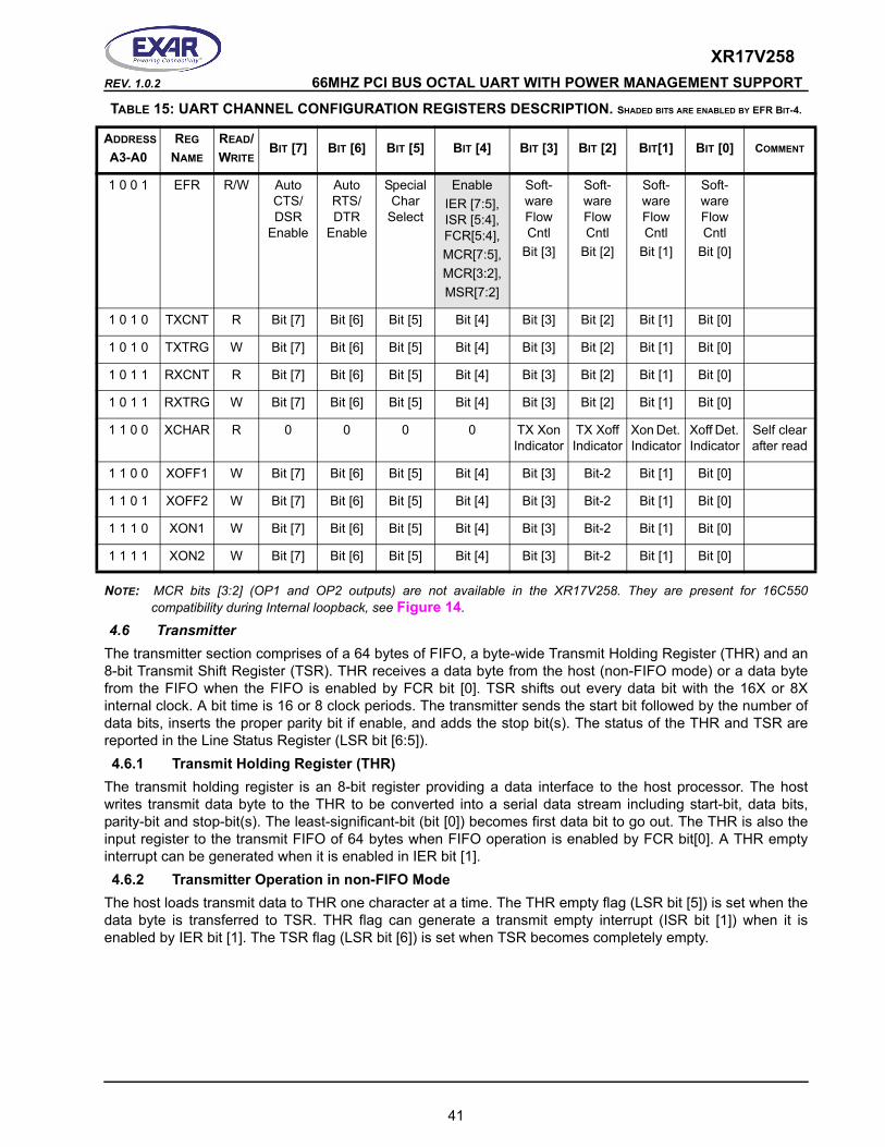
XR17V258REV. 1.0.2 66MHZ PCI BUS OCTAL UART WITH POWER MANAGEMENT SUPPORT
NOTE: MCR bits [3:2] (OP1 and OP2 outputs) are not available in the XR17V258. They are present for 16C550 compatibility during Internal loopback, see Figure 14.
4.6 Transmitter The transmitter section comprises of a 64 bytes of FIFO, a byte-wide Transmit Holding Register (THR) and an 8-bit Transmit Shift Register (TSR). THR receives a data byte from the host (non-FIFO mode) or a data byte from the FIFO when the FIFO is enabled by FCR bit [0]. TSR shifts out every data bit with the 16X or 8X internal clock. A bit time is 16 or 8 clock periods. The transmitter sends the start bit followed by the number of data bits, inserts the proper parity bit if enable, and adds the stop bit(s). The status of the THR and TSR are reported in the Line Status Register (LSR bit [6:5]). 4.6.1 Transmit Holding Register (THR)
The transmit holding register is an 8-bit register providing a data interface to the host processor. The host writes transmit data byte to the THR to be converted into a serial data stream including start-bit, data bits, parity-bit and stop-bit(s). The least-significant-bit (bit [0]) becomes first data bit to go out. The THR is also the input register to the transmit FIFO of 64 bytes when FIFO operation is enabled by FCR bit[0]. A THR empty interrupt can be generated when it is enabled in IER bit [1].4.6.2 Transmitter Operation in non-FIFO Mode
The host loads transmit data to THR one character at a time. The THR empty flag (LSR bit [5]) is set when the data byte is transferred to TSR. THR flag can generate a transmit empty interrupt (ISR bit [1]) when it is enabled by IER bit [1]. The TSR flag (LSR bit [6]) is set when TSR becomes completely empty.
1 0 0 1 EFR R/W Auto CTS/DSR
Enable
Auto RTS/DTR
Enable
Special Char
Select
Enable IER [7:5], ISR [5:4], FCR[5:4],MCR[7:5],MCR[3:2],MSR[7:2]
Soft-ware Flow Cntl
Bit [3]
Soft-ware Flow Cntl
Bit [2]
Soft-ware Flow Cntl
Bit [1]
Soft-ware Flow Cntl
Bit [0]
1 0 1 0 TXCNT R Bit [7] Bit [6] Bit [5] Bit [4] Bit [3] Bit [2] Bit [1] Bit [0]
1 0 1 0 TXTRG W Bit [7] Bit [6] Bit [5] Bit [4] Bit [3] Bit [2] Bit [1] Bit [0]
1 0 1 1 RXCNT R Bit [7] Bit [6] Bit [5] Bit [4] Bit [3] Bit [2] Bit [1] Bit [0]
1 0 1 1 RXTRG W Bit [7] Bit [6] Bit [5] Bit [4] Bit [3] Bit [2] Bit [1] Bit [0]
1 1 0 0 XCHAR R 0 0 0 0 TX Xon Indicator
TX Xoff Indicator
Xon Det. Indicator
Xoff Det. Indicator
Self clear after read
1 1 0 0 XOFF1 W Bit [7] Bit [6] Bit [5] Bit [4] Bit [3] Bit-2 Bit [1] Bit [0]
1 1 0 1 XOFF2 W Bit [7] Bit [6] Bit [5] Bit [4] Bit [3] Bit-2 Bit [1] Bit [0]
1 1 1 0 XON1 W Bit [7] Bit [6] Bit [5] Bit [4] Bit [3] Bit-2 Bit [1] Bit [0]
1 1 1 1 XON2 W Bit [7] Bit [6] Bit [5] Bit [4] Bit [3] Bit-2 Bit [1] Bit [0]
TABLE 15: UART CHANNEL CONFIGURATION REGISTERS DESCRIPTION. SHADED BITS ARE ENABLED BY EFR BIT-4.
ADDRESS
A3-A0REG
NAME
READ/WRITE
BIT [7] BIT [6] BIT [5] BIT [4] BIT [3] BIT [2] BIT[1] BIT [0] COMMENT
41
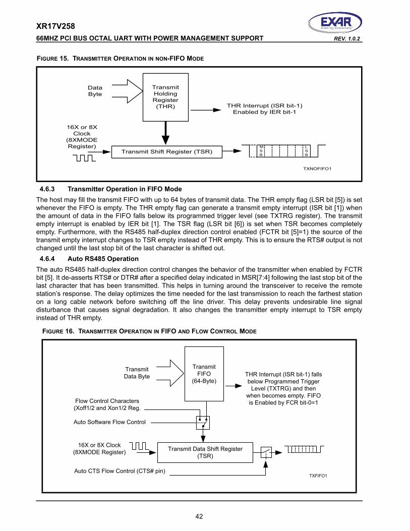
XR17V258 66MHZ PCI BUS OCTAL UART WITH POWER MANAGEMENT SUPPORT REV. 1.0.2
FIGURE 15. TRANSMITTER OPERATION IN NON-FIFO MODE
TransmitHoldingRegister(THR)
Transmit Shift Register (TSR)
DataByte
LSB
MSB
THR Interrupt (ISR bit-1)Enabled by IER bit-1
TXNOFIFO1
16X or 8XClock
(8XMODERegister)
4.6.3 Transmitter Operation in FIFO ModeThe host may fill the transmit FIFO with up to 64 bytes of transmit data. The THR empty flag (LSR bit [5]) is set whenever the FIFO is empty. The THR empty flag can generate a transmit empty interrupt (ISR bit [1]) when the amount of data in the FIFO falls below its programmed trigger level (see TXTRG register). The transmit empty interrupt is enabled by IER bit [1]. The TSR flag (LSR bit [6]) is set when TSR becomes completely empty. Furthermore, with the RS485 half-duplex direction control enabled (FCTR bit [5]=1) the source of the transmit empty interrupt changes to TSR empty instead of THR empty. This is to ensure the RTS# output is not changed until the last stop bit of the last character is shifted out.4.6.4 Auto RS485 Operation
The auto RS485 half-duplex direction control changes the behavior of the transmitter when enabled by FCTR bit [5]. It de-asserts RTS# or DTR# after a specified delay indicated in MSR[7:4] following the last stop bit of the last character that has been transmitted. This helps in turning around the transceiver to receive the remote station’s response. The delay optimizes the time needed for the last transmission to reach the farthest station on a long cable network before switching off the line driver. This delay prevents undesirable line signal disturbance that causes signal degradation. It also changes the transmitter empty interrupt to TSR empty instead of THR empty.
FIGURE 16. TRANSMITTER OPERATION IN FIFO AND FLOW CONTROL MODE
Transmit Data Shift Register(TSR)
TransmitData Byte THR Interrupt (ISR bit-1) falls
below Programmed TriggerLevel (TXTRG) and then
when becomes empty. FIFOis Enabled by FCR bit-0=1
TransmitFIFO
(64-Byte)
TXFIFO1
16X or 8X Clock(8XMODE Register)
Auto CTS Flow Control (CTS# pin)
Auto Software Flow Control
Flow Control Characters(Xoff1/2 and Xon1/2 Reg.
42
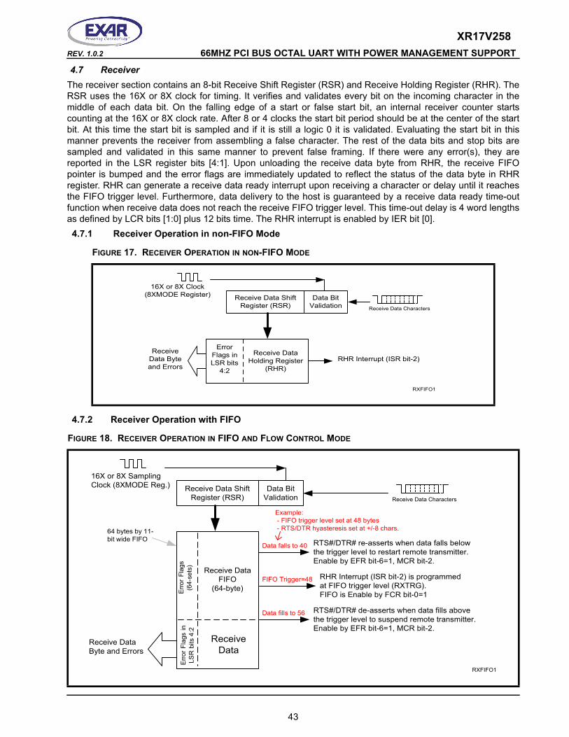
XR17V258REV. 1.0.2 66MHZ PCI BUS OCTAL UART WITH POWER MANAGEMENT SUPPORT
4.7 ReceiverThe receiver section contains an 8-bit Receive Shift Register (RSR) and Receive Holding Register (RHR). The RSR uses the 16X or 8X clock for timing. It verifies and validates every bit on the incoming character in the middle of each data bit. On the falling edge of a start or false start bit, an internal receiver counter starts counting at the 16X or 8X clock rate. After 8 or 4 clocks the start bit period should be at the center of the start bit. At this time the start bit is sampled and if it is still a logic 0 it is validated. Evaluating the start bit in this manner prevents the receiver from assembling a false character. The rest of the data bits and stop bits are sampled and validated in this same manner to prevent false framing. If there were any error(s), they are reported in the LSR register bits [4:1]. Upon unloading the receive data byte from RHR, the receive FIFO pointer is bumped and the error flags are immediately updated to reflect the status of the data byte in RHR register. RHR can generate a receive data ready interrupt upon receiving a character or delay until it reaches the FIFO trigger level. Furthermore, data delivery to the host is guaranteed by a receive data ready time-out function when receive data does not reach the receive FIFO trigger level. This time-out delay is 4 word lengths as defined by LCR bits [1:0] plus 12 bits time. The RHR interrupt is enabled by IER bit [0].4.7.1 Receiver Operation in non-FIFO Mode
FIGURE 17. RECEIVER OPERATION IN NON-FIFO MODE
Receive Data ShiftRegister (RSR)
ReceiveData Byteand Errors
RHR Interrupt (ISR bit-2)Receive Data
Holding Register(RHR)
RXFIFO1
16X or 8X Clock(8XMODE Register)
Receive Data Characters
Data BitValidation
ErrorFlags inLSR bits
4:2
4.7.2 Receiver Operation with FIFO
FIGURE 18. RECEIVER OPERATION IN FIFO AND FLOW CONTROL MODE
Receive Data ShiftRegister (RSR)
RXFIFO1
16X or 8X SamplingClock (8XMODE Reg.)
Erro
r Fl
ags
(64-
sets
)E
rror
Flag
s in
LSR
bits
4:2
64 bytes by 11-bit wide FIFO
Receive Data Characters
FIFO Trigger=48
Example: - FIFO trigger level set at 48 bytes - RTS/DTR hyasteresis set at +/-8 chars.
Data fills to 56
Data falls to 40
Data BitValidation
Receive DataFIFO
(64-byte)
ReceiveData
Receive DataByte and Errors
RHR Interrupt (ISR bit-2) is programmedat FIFO trigger level (RXTRG).FIFO is Enable by FCR bit-0=1
RTS#/DTR# de-asserts when data fills abovethe trigger level to suspend remote transmitter.Enable by EFR bit-6=1, MCR bit-2.
RTS#/DTR# re-asserts when data falls belowthe trigger level to restart remote transmitter.Enable by EFR bit-6=1, MCR bit-2.
43
XR17V258 66MHZ PCI BUS OCTAL UART WITH POWER MANAGEMENT SUPPORT REV. 1.0.2
5.0 UART CONFIGURATION REGISTERS5.1 Receive Holding Register (RHR) - Read only
SEE”RECEIVER” ON PAGE 43.5.2 Transmit Holding Register (THR) - Write only
SEE”TRANSMITTER” ON PAGE 41.5.3 Baud Rate Generator Divisors (DLM, DLL and DLD)
The Baud Rate Generator (BRG) generates the data rate for the transmitter and receiver. The rate is programmed through registers DLM, DLL and DLD which are only accessible when LCR bit [7] is set to logic 1. Refer to “Section 4.1, Programmable Baud Rate Generator with Fractional Divisor” on page 31 for more details.5.4 Interrupt Enable Register (IER) - Read/Write
The Interrupt Enable Register (IER) masks the interrupts from receive data ready, transmit empty, line status and modem status registers. These interrupts are reported in the Interrupt Status Register (ISR) and also encoded in INT (INT0-INT3) register in the Device Configuration Registers. 5.4.1 IER versus Receive FIFO Interrupt Mode Operation
When the receive FIFO (FCR bit [0] = logic 1) and receive interrupts (IER bit [0] = logic 1) are enabled, the RHR interrupts (see ISR bits [4:3]) status will reflect the following:A. The receive data available interrupts are issued to the host when the FIFO has reached the programmed
trigger level. It will be cleared when the FIFO drops below the programmed trigger level.B. FIFO level will be reflected in the ISR register when the FIFO trigger level is reached. Both the ISR register
status bit and the interrupt will be cleared when the FIFO drops below the trigger level.C. The receive data ready bit (LSR bit [0]) is set as soon as a character is transferred from the shift register to
the receive FIFO. It is reset when the FIFO is empty.5.4.2 IER versus Receive/Transmit FIFO Polled Mode Operation
When FCR bit [0] equals a logic 1 for FIFO enable; resetting IER bits [3:0] enables the XR16V258 in the FIFO polled mode of operation. Since the receiver and transmitter have separate bits in the LSR either can be used in the polled mode by selecting respective transmit or receive control bit(s).A. LSR BIT-0 indicates there is data in RHR (non-FIFO mode) or RX FIFO (FIFO mode).B. LSR BIT-1 indicates an overrun error has occurred and that data in the FIFO may not be valid.C. LSR BIT 2-4 provides the type of receive data errors encountered for the data byte in RHR, if any.D. LSR BIT-5 indicates THR (non-FIFO mode) or TX FIFO (FIFO mode) is empty.E. LSR BIT-6 indicates when both the transmit FIFO and TSR are empty.F. LSR BIT-7 indicates a data error in at least one character in the RX FIFO.IER[7]: CTS# Input Interrupt Enable (requires EFR bit [4]=1)
• Logic 0 = Disable the CTS# interrupt (default).• Logic 1 = Enable the CTS# interrupt. The UART issues an interrupt when CTS# pin makes a transition from
LOW to HIGH.IER[6]: RTS# Output Interrupt Enable (requires EFR bit [4]=1)
• Logic 0 = Disable the RTS# interrupt (default).• Logic 1 = Enable the RTS# interrupt. The UART issues an interrupt when RTS# pin makes a transition from
LOW to HIGH.IER[5]: Xoff Interrupt Enable (requires EFR bit [4]=1)
• Logic 0 = Disable the software flow control, receive Xoff interrupt (default).• Logic 1 = Enable the software flow control, receive Xoff interrupt. See Software Flow Control section for
details.
44
XR17V258REV. 1.0.2 66MHZ PCI BUS OCTAL UART WITH POWER MANAGEMENT SUPPORT
IER[4]: Reserved
IER[3]: Modem Status Interrupt EnableThe Modem Status Register interrupt is issued whenever any of the delta bits of the MSR register (bits [3:0]) is set.
• Logic 0 = Disable the modem status register interrupt (default).• Logic 1 = Enable the modem status register interrupt.
IER[2]: Receive Line Status Interrupt EnableAn Overrun error, Framing error, Parity error or detection of a Break character will result in an LSR interrupt. The V258 will issue an LSR interrupt immediately after receiving a character with an error. It will again re-issue the interrupt (if the first one has been cleared by reading the LSR register) when the character with the error is on the top of the FIFO, meaning the next one to be read out of the FIFO.For example, let’s consider an incoming data stream of 0x55, 0xAA, etc. and that the character 0xAA has a Parity error associated with it. Let’s assume that the character 0x55 has not been read out of the FIFO yet. The V258v258 will issue an interrupt as soon as the stop bit of the character 0xAA is received. The LSR register will have only the FIFO error bit (bit [7]) set and none of the other error bits (bits [4:1]) will be set, since the byte on the top of the FIFO is 0x55 which does not have any errors associated with it. When this byte has been read out, the V258 will issue another LSR interrupt and this time the LSR register will show the Parity bit (bit [2]) set.
• Logic 0 = Disable the receiver line status interrupt (default).• Logic 1 = Enable the receiver line status interrupt.
IER[1]: TX Ready Interrupt EnableIn non-FIFO mode, a TX interrupt is issued whenever the THR is empty. In the FIFO mode, an interrupt is issued twice: once when the number of bytes in the TX FIFO falls below the programmed trigger level and again when the TX FIFO becomes empty. When autoRS485 mode is enabled (FCTR bit [5] = 1), the second interrupt is delayed until the transmitter (both the TX FIFO and the TX Shift Register) is empty.
• Logic 0= Disable Transmit Ready Interrupt (default).• Logic 1 = Enable Transmit Ready Interrupt.
IER[0]: RX Interrupt EnableThe receive data ready interrupt will be issued when RHR has a data character in the non-FIFO mode or when the receive FIFO has reached the programmed trigger level in the FIFO mode.
• Logic 0 = Disable the receive data ready interrupt (default).• Logic 1 = Enable the receiver data ready interrupt.
5.5 Interrupt Status Register (ISR) - Read OnlyThe UART provides multiple levels of prioritized interrupts to minimize external software interaction. The Interrupt Status Register (ISR) provides the user with six interrupt status bits. Performing a read cycle on the ISR will give the user the current highest pending interrupt level to be serviced, others queue up for next service. No other interrupts are acknowledged until the pending interrupt is serviced. The Interrupt Source Table, Table 16, shows the data values (bit [5:0]) for the six prioritized interrupt levels and the interrupt sources associated with each of these interrupt levels.
45
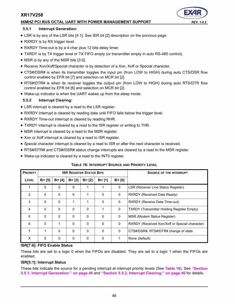
XR17V258 66MHZ PCI BUS OCTAL UART WITH POWER MANAGEMENT SUPPORT REV. 1.0.2
5.5.1 Interrupt Generation:
• LSR is by any of the LSR bits [4:1]. See IER bit [2] description on the previous page.• RXRDY is by RX trigger level.• RXRDY Time-out is by a 4-char plus 12 bits delay timer.• TXRDY is by TX trigger level or TX FIFO empty (or transmitter empty in auto RS-485 control).• MSR is by any of the MSR bits [3:0].• Receive Xon/Xoff/Special character is by detection of a Xon, Xoff or Special character.• CTS#/DSR# is when its transmitter toggles the input pin (from LOW to HIGH) during auto CTS/DSR flow
control enabled by EFR bit [7] and selection on MCR bit [2].• RTS#/DTR# is when its receiver toggles the output pin (from LOW to HIGH) during auto RTS/DTR flow
control enabled by EFR bit [6] and selection on MCR bit [2]. • Wake-up indicator is when the UART wakes up from the sleep mode.
5.5.2 Interrupt Clearing:
• LSR interrupt is cleared by a read to the LSR register.• RXRDY interrupt is cleared by reading data until FIFO falls below the trigger level.• RXRDY Time-out interrupt is cleared by reading RHR.• TXRDY interrupt is cleared by a read to the ISR register or writing to THR.• MSR interrupt is cleared by a read to the MSR register.• Xon or Xoff interrupt is cleared by a read to ISR register.• Special character interrupt is cleared by a read to ISR or after the next character is received.• RTS#/DTR# and CTS#/DSR# status change interrupts are cleared by a read to the MSR register.• Wake-up indicator is cleared by a read to the INT0 register.]
TABLE 16: INTERRUPT SOURCE AND PRIORITY LEVEL
PRIORITY ISR REGISTER STATUS BITS SOURCE OF THE INTERRUPT
LEVEL BIT [5] BIT [4] BIT [3] BIT [2] BIT [1] BIT [0]
1 0 0 0 1 1 0 LSR (Receiver Line Status Register)
2 0 0 0 1 0 0 RXRDY (Received Data Ready)
3 0 0 1 1 0 0 RXRDY (Receive Data Time-out)
4 0 0 0 0 1 0 TXRDY (Transmitter Holding Register Empty)
5 0 0 0 0 0 0 MSR (Modem Status Register)
6 0 1 0 0 0 0 RXRDY (Received Xon/Xoff or Special character)
7 1 0 0 0 0 0 CTS#/DSR#, RTS#/DTR# change of state
X 0 0 0 0 0 1 None (default)
ISR[7:6]: FIFO Enable StatusThese bits are set to a logic 0 when the FIFOs are disabled. They are set to a logic 1 when the FIFOs are enabled. ISR[5:1]: Interrupt StatusThese bits indicate the source for a pending interrupt at interrupt priority levels (See Table 16). See “Section 5.5.1, Interrupt Generation:” on page 46 and “Section 5.5.2, Interrupt Clearing:” on page 46 for details.
46
XR17V258REV. 1.0.2 66MHZ PCI BUS OCTAL UART WITH POWER MANAGEMENT SUPPORT
ISR[0]: Interrupt Status
• Logic 0 = An interrupt is pending and the ISR contents may be used as a pointer to the appropriate interrupt service routine.
• Logic 1 = No interrupt pending. (default condition)
5.6 FIFO Control Register (FCR) - Write OnlyThis register is used to enable the FIFOs, clear the FIFOs, set the transmit/receive FIFO trigger levels, and select the DMA mode. The DMA, and FIFO modes are defined as follows:FCR[7:6]: Receive FIFO Trigger Select(logic 0 = default, RX trigger level =1)The FCTR bits [5:4] are associated with these 2 bits. These 2 bits are used to set the trigger level for the receive FIFO. The UART will issue a receive interrupt when the number of the characters in the FIFO crosses the trigger level. Table 17 shows the complete selections. Note that the receiver and the transmitter cannot use different trigger tables. Whichever selection is made last applies to both the RX and TX side.FCR[5:4]: Transmit FIFO Trigger Select (requires EFR bit [4]=1)(logic 0 = default, TX trigger level = 1)The FCTR bits [7:6] are associated with these 2 bits by selecting one of the four tables. The 4 user selectable trigger levels in 4 tables are supported for compatibility reasons. These 2 bits set the trigger level for the transmit FIFO interrupt. The UART will issue a transmit interrupt when the number of characters in the FIFO falls below the selected trigger level, or when it gets empty in case that the FIFO did not get filled over the trigger level on last re-load. Table 17 below shows the selections. FCR[3]: DMA Mode SelectThis bit has no effect since TXRDY and RXRDY pins are not available in this device. It is provided for legacy software compatibility.
• Logic 0 = Set DMA to mode 0 (default).• Logic 1 = Set DMA to mode 1.
FCR[2]: TX FIFO ResetThis bit is only active when FCR bit [0] is active.
• Logic 0= No transmit FIFO reset (default).• Logic 1 = Reset the transmit FIFO pointers and FIFO level counter logic (the transmit shift register is not
cleared or altered). This bit will return to a logic 0 after resetting the FIFO.FCR[1]: RX FIFO ResetThis bit is only active when FCR bit [0] is active.
• Logic 0 = No receive FIFO reset (default).• Logic 1 = Reset the receive FIFO pointers and FIFO level counter logic (the receive shift register is not
cleared or altered). This bit will return to a logic 0 after resetting the FIFO.FCR[0]: TX and RX FIFO Enable
• Logic 0 = Disable the transmit and receive FIFO (default).• Logic 1 = Enable the transmit and receive FIFOs. This bit must be set to logic 1 when other FCR bits are
written or they will not be programmed.
47
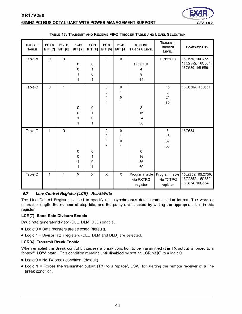
XR17V258 66MHZ PCI BUS OCTAL UART WITH POWER MANAGEMENT SUPPORT REV. 1.0.2
TABLE 17: TRANSMIT AND RECEIVE FIFO TRIGGER TABLE AND LEVEL SELECTION
TRIGGER TABLE
RECEIVE TRIGGER LEVEL
TRANSMIT TRIGGER LEVEL
COMPATIBILITY
Table-A 0 00011
0101
0 01 (default)
4814
1 (default) 16C550, 16C2550, 16C2552, 16C554, 16C580, 16L580
Table-B 0 1
0011
0101
0011
0101
8162428
1682430
16C650A, 16L651
Table-C 1 0
0011
0101
0011
0101
8165660
8163256
16C654
Table-D 1 1 X X X X Programmablevia RXTRG
register
Programmable via TXTRG
register
16L2752, 16L2750, 16C2852, 16C850, 16C854, 16C864
5.7 Line Control Register (LCR) - Read/WriteThe Line Control Register is used to specify the asynchronous data communication format. The word or character length, the number of stop bits, and the parity are selected by writing the appropriate bits in this register. LCR[7]: Baud Rate Divisors EnableBaud rate generator divisor (DLL, DLM, DLD) enable.
• Logic 0 = Data registers are selected (default).• Logic 1 = Divisor latch registers (DLL, DLM and DLD) are selected.
LCR[6]: Transmit Break EnableWhen enabled the Break control bit causes a break condition to be transmitted (the TX output is forced to a “space", LOW, state). This condition remains until disabled by setting LCR bit [6] to a logic 0.
• Logic 0 = No TX break condition. (default)• Logic 1 = Forces the transmitter output (TX) to a “space”, LOW, for alerting the remote receiver of a line
break condition.
FCTR BIT [7]
FCTR BIT [6]
FCR BIT [7]
FCR BIT [6]
FCR BIT [5]
FCR BIT [4]
48
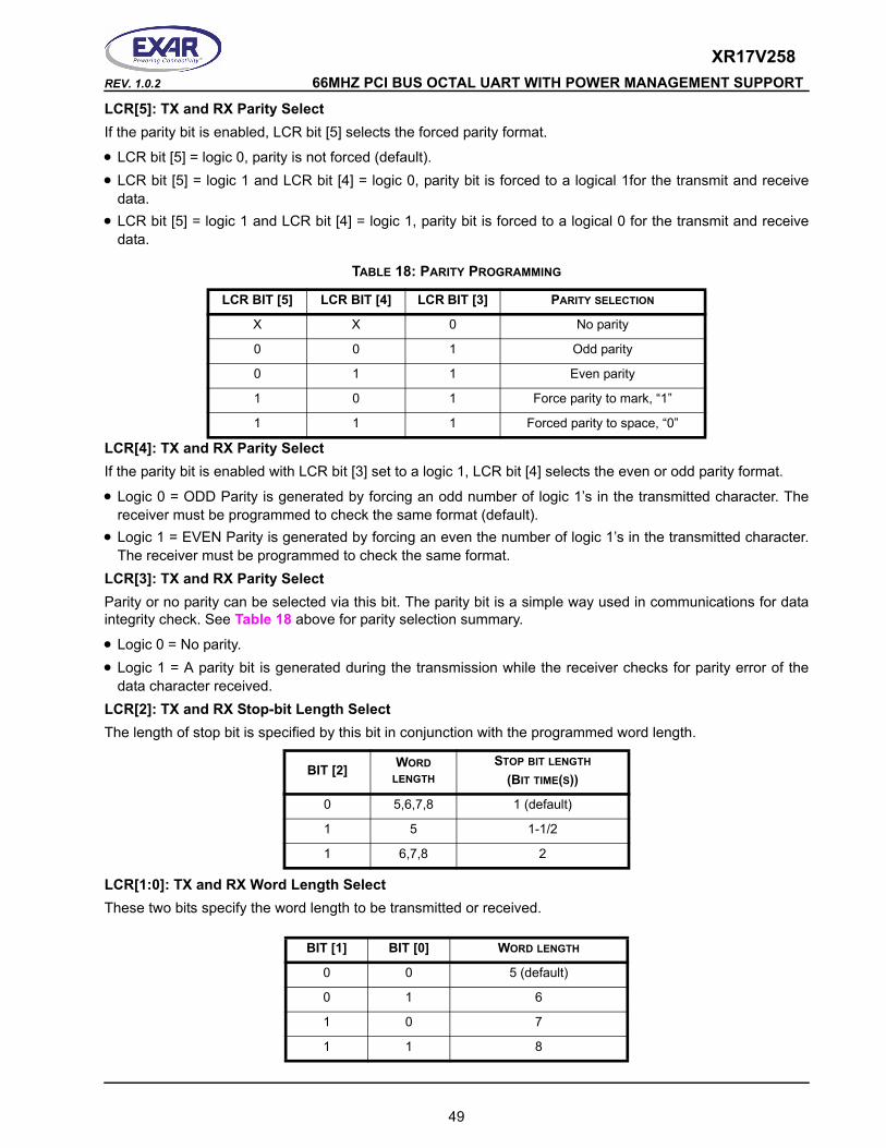
XR17V258REV. 1.0.2 66MHZ PCI BUS OCTAL UART WITH POWER MANAGEMENT SUPPORT
LCR[5]: TX and RX Parity SelectIf the parity bit is enabled, LCR bit [5] selects the forced parity format.
• LCR bit [5] = logic 0, parity is not forced (default).• LCR bit [5] = logic 1 and LCR bit [4] = logic 0, parity bit is forced to a logical 1for the transmit and receive
data.• LCR bit [5] = logic 1 and LCR bit [4] = logic 1, parity bit is forced to a logical 0 for the transmit and receive
data.
TABLE 18: PARITY PROGRAMMING
BIT [5] BIT [4] BIT [3] PARITY SELECTION
X X 0 No parity
0 0 1 Odd parity
0 1 1 Even parity
1 0 1 Force parity to mark, “1”
1 1 1 Forced parity to space, “0”
LCR[4]: TX and RX Parity SelectIf the parity bit is enabled with LCR bit [3] set to a logic 1, LCR bit [4] selects the even or odd parity format.
• Logic 0 = ODD Parity is generated by forcing an odd number of logic 1’s in the transmitted character. The receiver must be programmed to check the same format (default).
• Logic 1 = EVEN Parity is generated by forcing an even the number of logic 1’s in the transmitted character. The receiver must be programmed to check the same format.
LCR[3]: TX and RX Parity SelectParity or no parity can be selected via this bit. The parity bit is a simple way used in communications for data integrity check. See Table 18 above for parity selection summary.
• Logic 0 = No parity. • Logic 1 = A parity bit is generated during the transmission while the receiver checks for parity error of the
data character received.LCR[2]: TX and RX Stop-bit Length SelectThe length of stop bit is specified by this bit in conjunction with the programmed word length.
WORD LENGTH
STOP BIT LENGTH
(BIT TIME(S))
0 5,6,7,8 1 (default)
1 5 1-1/2
1 6,7,8 2
LCR[1:0]: TX and RX Word Length SelectThese two bits specify the word length to be transmitted or received.
WORD LENGTH
0 0 5 (default)
0 1 6
1 0 7
1 1 8
LCR LCR LCR
BIT [2]
BIT [1] BIT [0]
49
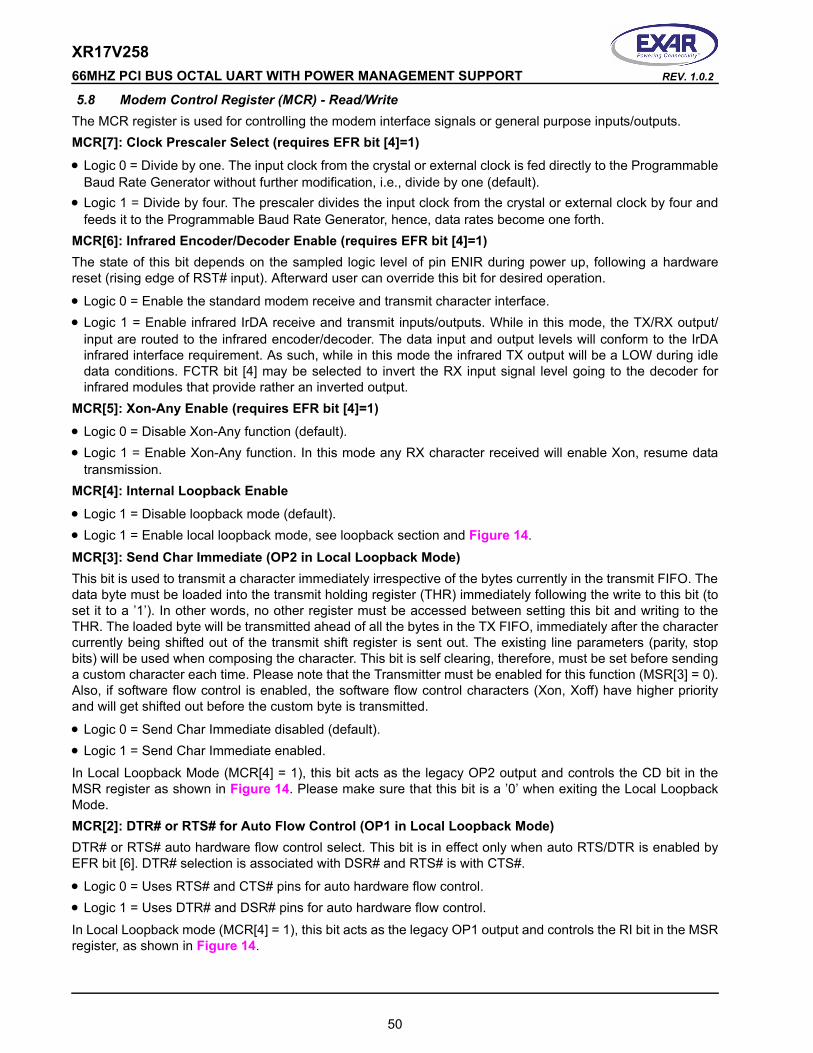
XR17V258 66MHZ PCI BUS OCTAL UART WITH POWER MANAGEMENT SUPPORT REV. 1.0.2
5.8 Modem Control Register (MCR) - Read/WriteThe MCR register is used for controlling the modem interface signals or general purpose inputs/outputs.MCR[7]: Clock Prescaler Select (requires EFR bit [4]=1)
• Logic 0 = Divide by one. The input clock from the crystal or external clock is fed directly to the Programmable Baud Rate Generator without further modification, i.e., divide by one (default).
• Logic 1 = Divide by four. The prescaler divides the input clock from the crystal or external clock by four and feeds it to the Programmable Baud Rate Generator, hence, data rates become one forth.
MCR[6]: Infrared Encoder/Decoder Enable (requires EFR bit [4]=1)The state of this bit depends on the sampled logic level of pin ENIR during power up, following a hardware reset (rising edge of RST# input). Afterward user can override this bit for desired operation.
• Logic 0 = Enable the standard modem receive and transmit character interface.• Logic 1 = Enable infrared IrDA receive and transmit inputs/outputs. While in this mode, the TX/RX output/
input are routed to the infrared encoder/decoder. The data input and output levels will conform to the IrDA infrared interface requirement. As such, while in this mode the infrared TX output will be a LOW during idle data conditions. FCTR bit [4] may be selected to invert the RX input signal level going to the decoder for infrared modules that provide rather an inverted output.
MCR[5]: Xon-Any Enable (requires EFR bit [4]=1)
• Logic 0 = Disable Xon-Any function (default).• Logic 1 = Enable Xon-Any function. In this mode any RX character received will enable Xon, resume data
transmission. MCR[4]: Internal Loopback Enable
• Logic 1 = Disable loopback mode (default).• Logic 1 = Enable local loopback mode, see loopback section and Figure 14.
MCR[3]: Send Char Immediate (OP2 in Local Loopback Mode)This bit is used to transmit a character immediately irrespective of the bytes currently in the transmit FIFO. The data byte must be loaded into the transmit holding register (THR) immediately following the write to this bit (to set it to a ’1’). In other words, no other register must be accessed between setting this bit and writing to the THR. The loaded byte will be transmitted ahead of all the bytes in the TX FIFO, immediately after the character currently being shifted out of the transmit shift register is sent out. The existing line parameters (parity, stop bits) will be used when composing the character. This bit is self clearing, therefore, must be set before sending a custom character each time. Please note that the Transmitter must be enabled for this function (MSR[3] = 0). Also, if software flow control is enabled, the software flow control characters (Xon, Xoff) have higher priority and will get shifted out before the custom byte is transmitted.
• Logic 0 = Send Char Immediate disabled (default).• Logic 1 = Send Char Immediate enabled.
In Local Loopback Mode (MCR[4] = 1), this bit acts as the legacy OP2 output and controls the CD bit in the MSR register as shown in Figure 14. Please make sure that this bit is a ’0’ when exiting the Local Loopback Mode.MCR[2]: DTR# or RTS# for Auto Flow Control (OP1 in Local Loopback Mode)DTR# or RTS# auto hardware flow control select. This bit is in effect only when auto RTS/DTR is enabled by EFR bit [6]. DTR# selection is associated with DSR# and RTS# is with CTS#.
• Logic 0 = Uses RTS# and CTS# pins for auto hardware flow control. • Logic 1 = Uses DTR# and DSR# pins for auto hardware flow control.
In Local Loopback mode (MCR[4] = 1), this bit acts as the legacy OP1 output and controls the RI bit in the MSR register, as shown in Figure 14.
50
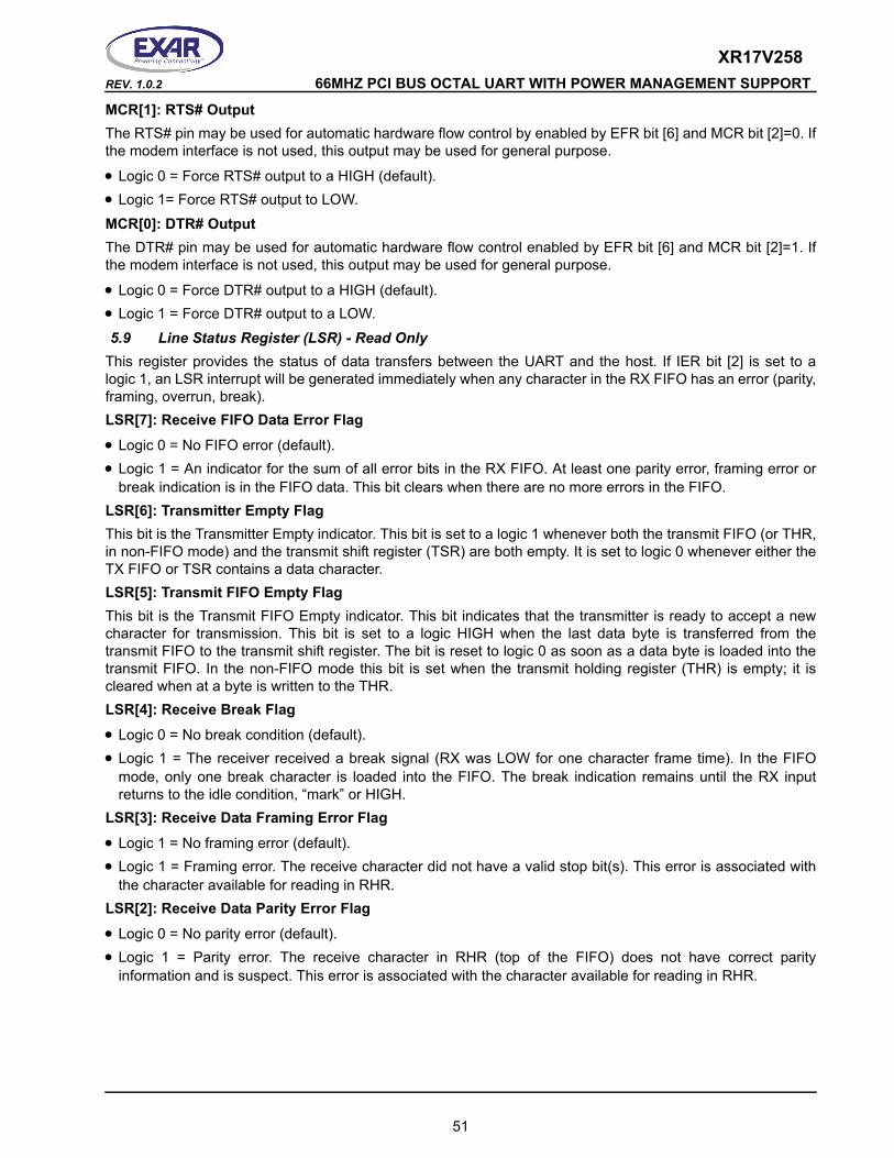
XR17V258REV. 1.0.2 66MHZ PCI BUS OCTAL UART WITH POWER MANAGEMENT SUPPORT
MCR[1]: RTS# OutputThe RTS# pin may be used for automatic hardware flow control by enabled by EFR bit [6] and MCR bit [2]=0. If the modem interface is not used, this output may be used for general purpose.
• Logic 0 = Force RTS# output to a HIGH (default).• Logic 1= Force RTS# output to LOW.
MCR[0]: DTR# OutputThe DTR# pin may be used for automatic hardware flow control enabled by EFR bit [6] and MCR bit [2]=1. If the modem interface is not used, this output may be used for general purpose.
• Logic 0 = Force DTR# output to a HIGH (default).• Logic 1 = Force DTR# output to a LOW.
5.9 Line Status Register (LSR) - Read OnlyThis register provides the status of data transfers between the UART and the host. If IER bit [2] is set to a logic 1, an LSR interrupt will be generated immediately when any character in the RX FIFO has an error (parity, framing, overrun, break).LSR[7]: Receive FIFO Data Error Flag
• Logic 0 = No FIFO error (default).• Logic 1 = An indicator for the sum of all error bits in the RX FIFO. At least one parity error, framing error or
break indication is in the FIFO data. This bit clears when there are no more errors in the FIFO. LSR[6]: Transmitter Empty FlagThis bit is the Transmitter Empty indicator. This bit is set to a logic 1 whenever both the transmit FIFO (or THR, in non-FIFO mode) and the transmit shift register (TSR) are both empty. It is set to logic 0 whenever either the TX FIFO or TSR contains a data character.LSR[5]: Transmit FIFO Empty FlagThis bit is the Transmit FIFO Empty indicator. This bit indicates that the transmitter is ready to accept a new character for transmission. This bit is set to a logic HIGH when the last data byte is transferred from the transmit FIFO to the transmit shift register. The bit is reset to logic 0 as soon as a data byte is loaded into the transmit FIFO. In the non-FIFO mode this bit is set when the transmit holding register (THR) is empty; it is cleared when at a byte is written to the THR.LSR[4]: Receive Break Flag
• Logic 0 = No break condition (default).• Logic 1 = The receiver received a break signal (RX was LOW for one character frame time). In the FIFO
mode, only one break character is loaded into the FIFO. The break indication remains until the RX input returns to the idle condition, “mark” or HIGH.
LSR[3]: Receive Data Framing Error Flag
• Logic 1 = No framing error (default).• Logic 1 = Framing error. The receive character did not have a valid stop bit(s). This error is associated with
the character available for reading in RHR.LSR[2]: Receive Data Parity Error Flag
• Logic 0 = No parity error (default).• Logic 1 = Parity error. The receive character in RHR (top of the FIFO) does not have correct parity
information and is suspect. This error is associated with the character available for reading in RHR.
51
XR17V258 66MHZ PCI BUS OCTAL UART WITH POWER MANAGEMENT SUPPORT REV. 1.0.2
LSR[1]: Receiver Overrun Flag
• Logic 0 = No overrun error (default).• Logic 1 = Overrun error. A data overrun error condition occurred in the receive shift register. This happens
when additional data arrives while the FIFO is full. In this case the previous data in the receive shift register is overwritten. Note that under this condition the data byte in the receive shift register is not transferred into the FIFO, therefore the data in the FIFO is not corrupted by the error.
LSR[0]: Receive Data Ready Indicator
• Logic 0 = No data in receive holding register or FIFO (default).• Logic 1 = Data has been received and is saved in the receive holding register or FIFO.
5.10 Modem Status Register (MSR) - Read OnlyThis register provides the current state of the modem interface signals, or other peripheral device that the UART is connected. Lower four bits of this register are used to indicate the changed information. These bits are set to a logic 1 whenever a signal from the modem changes state. These bits may be used as general purpose inputs/outputs when they are not used with modem signals.MSR[7]: CD Input StatusNormally this bit is the complement of the CD# input. In the loopback mode this bit is equivalent to bit [3] in the MCR register. The CD# input may be used as a general purpose input when the modem interface is not used.MSR[6]: RI Input StatusNormally this bit is the complement of the RI# input. In the loopback mode this bit is equivalent to bit [2] in the MCR register. The RI# input may be used as a general purpose input when the modem interface is not used.MSR[5]: DSR Input StatusDSR# pin may function as automatic hardware flow control signal input if it is enabled and selected by Auto CTS/DSR bit (EFR bit [6]=1) and RTS/DTR flow control select bit (MCR bit [2]=1). Auto CTS/DSR flow control allows starting and stopping of local data transmissions based on the modem DSR# signal. A HIGH on the DSR# pin will stop UART transmitter as soon as the current character has finished transmission, and a LOW will resume data transmission. Normally MSR bit [5] is the complement of the DSR# input. However in the loopback mode, this bit is equivalent to the DTR# bit in the MCR register. The DSR# input may be used as a general purpose input when the modem interface is not used.MSR[4]: CTS Input StatusCTS# pin may function as automatic hardware flow control signal input if it is enabled and selected by Auto CTS/DSR bit (EFR bit [6]=1) and RTS/DTR flow control select bit (MCR bit [2]=0). Auto CTS/DSR flow control allows starting and stopping of local data transmissions based on the modem CTS# signal. A HIGH on the CTS# pin will stop UART transmitter as soon as the current character has finished transmission, and a LOW will resume data transmission. Normally MSR bit [4] is the complement of the CTS# input. However in the loopback mode, this bit is equivalent to the RTS# bit in the MCR register. The CTS# input may be used as a general purpose input when the modem interface is not used.MSR[3]: Delta CD# Input Flag
• Logic 0 = No change on CD# input (default).• Logic 1 = Indicates that the CD# input has changed state since the last time it was monitored. A modem
status interrupt will be generated if MSR interrupt is enabled (IER bit [3]).MSR[2]: Delta RI# Input Flag
• Logic 0 = No change on RI# input (default).• Logic 1 = The RI# input has changed from a LOW to a HIGH, ending of the ringing signal. A modem status
interrupt will be generated if MSR interrupt is enabled (IER bit [3]).
52
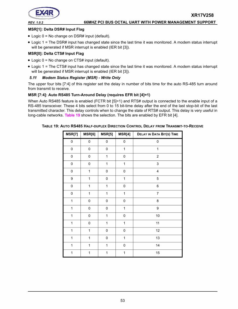
XR17V258REV. 1.0.2 66MHZ PCI BUS OCTAL UART WITH POWER MANAGEMENT SUPPORT
MSR[1]: Delta DSR# Input Flag
• Logic 0 = No change on DSR# input (default).• Logic 1 = The DSR# input has changed state since the last time it was monitored. A modem status interrupt
will be generated if MSR interrupt is enabled (IER bit [3]).MSR[0]: Delta CTS# Input Flag
• Logic 0 = No change on CTS# input (default).• Logic 1 = The CTS# input has changed state since the last time it was monitored. A modem status interrupt
will be generated if MSR interrupt is enabled (IER bit [3]).5.11 Modem Status Register (MSR) - Write Only
The upper four bits [7:4] of this register set the delay in number of bits time for the auto RS-485 turn around from transmit to receive.MSR [7:4]: Auto RS485 Turn-Around Delay (requires EFR bit [4]=1)When Auto RS485 feature is enabled (FCTR bit [5]=1) and RTS# output is connected to the enable input of a RS-485 transceiver. These 4 bits select from 0 to 15 bit-time delay after the end of the last stop-bit of the last transmitted character. This delay controls when to change the state of RTS# output. This delay is very useful in long-cable networks. Table 19 shows the selection. The bits are enabled by EFR bit [4].
TABLE 19: AUTO RS485 HALF-DUPLEX DIRECTION CONTROL DELAY FROM TRANSMIT-TO-RECEIVE
DELAY IN DATA BIT(S) TIME
0 0 0 0 0
0 0 0 1 1
0 0 1 0 2
0 0 1 1 3
0 1 0 0 4
9 1 0 1 5
0 1 1 0 6
0 1 1 1 7
1 0 0 0 8
1 0 0 1 9
1 0 1 0 10
1 0 1 1 11
1 1 0 0 12
1 1 0 1 13
1 1 1 0 14
1 1 1 1 15
MSR[7] MSR[6] MSR[5] MSR[4]
53
XR17V258 66MHZ PCI BUS OCTAL UART WITH POWER MANAGEMENT SUPPORT REV. 1.0.2
MSR [3]: Transmitter DisableThis bit can be used to disable the transmitter by halting the Transmit Shift Register (TSR). When this bit is set to a logic 1, the bytes already in the FIFO will not be sent out. Also, any more data loaded into the FIFO will stay in the FIFO and will not be sent out. When this bit is set to a logic 0, the bytes currently in the TX FIFO will be sent out. Please note that setting this bit to a logic 1 stops any character from going out. Also, this bit must be a logic 0 for the Send Char Immediate function (see MCR[3]).
• Logic 0 = Enable Transmitter (default).• Logic 1 = Disable Transmitter.
MSR [2]: Receiver DisableThis bit can be used to disable the receiver by halting the Receive Shift Register (RSR). When this bit is set to a logic 1, the receiver will operate in one of the following ways:
■ If a character is being received at the time of setting this bit, that character will be correctly received. No more characters will be received.
■ If the receiver is idle at the time of setting this bit, one character will still be received fully. No more characters will be received.
The receiver can be enabled and will start receiving characters by resetting this bit to a logic 0. The receiver will operate in one of the following ways:
■ If the receiver is idle (RX pin is HIGH) at the time of setting this bit, the next character will be received normally. It is recommended that the receiver be idle when resetting this bit to a logic 0.
■ If the receiver is not idle (RX pin is toggling) at the time of setting this bit, the RX FIFO will be filled with unknown data.
Any data that is in the RX FIFO can be read out at any time whether the receiver is disabled or not.
• Logic 0 = Enable Receiver (default).• Logic 1 = Disable Receiver.
MSR [1:0]: Reserved5.12 SCRATCH PAD REGISTER (SPR) - Read/Write
This is a 8-bit general purpose register for the user to store temporary data. The content of this register is preserved during sleep mode but becomes 0xFF (default) after a reset or a power off-on cycle. 5.13 FEATURE CONTROL REGISTER (FCTR) - Read/Write
This register controls the UART enhanced functions that are not available on ST16C554 or ST16C654.FCTR[7:6]: TX and RX FIFO Trigger Table Select These 2 bits select the transmit and receive FIFO trigger level table A, B, C or D. When table A, B, or C is selected the auto RTS flow control trigger level is set to "next FIFO trigger level" for compatibility to ST16C550 and ST16C650 series. RTS/DTR# triggers on the next level of the RX FIFO trigger level, in another word, one FIFO level above and one FIFO level below. See in Table 17 for complete selection with FCR bit [5:4] and FCTR bits [7:6], i.e. if Table C is used on the receiver with RX FIFO trigger level set to 56 bytes, RTS/DTR# output will de-assert at 60 and re-assert at 16.FCTR[5]: Auto RS485 EnableAuto RS485 half duplex control enable/disable.
• Logic 0 = Standard ST16C550 mode. Transmitter generates an interrupt when transmit holding register (THR) becomes empty. Transmit Shift Register (TSR) may still be shifting data bit out.
• Logic 1 = Enable Auto RS485 half duplex direction control. RTS# output changes from HIGH to LOW when finished sending the last stop bit of the last character out of the TSR register. It changes from LOW to HIGH when a data byte is loaded into the THR or transmit FIFO. The change to HIGH occurs prior sending the start-bit. It also changes the transmitter interrupt from transmit holding to transmit shift register (TSR) empty.
54
XR17V258REV. 1.0.2 66MHZ PCI BUS OCTAL UART WITH POWER MANAGEMENT SUPPORT
FCTR[4]: Infrared RX Input Logic Select
• Logic 0 = Select RX input as active HIGH encoded IrDA data, normal, (default).• Logic 1 = Select RX input as active LOW encoded IrDA data, inverted.
FCTR [3:0] - Auto RTS/DTR Flow Control Hysteresis SelectThese bits select the auto RTS/DTR flow control hysteresis and only valid when TX and RX Trigger Table-D is selected (FCTR bit [7:6] are set to logic 1). The RTS/DTR hysteresis is referenced to the RX FIFO trigger level. After reset, these bits are set to logic 0 selecting the next FIFO trigger level for hardware flow control. Table 20below shows the 16 selectable hysteresis levels.
TABLE 20: 16 SELECTABLE HYSTERESIS LEVELS WHEN TRIGGER TABLE-D IS SELECTED
FCTR BIT [3] FCTR BIT [2] FCTR BIT [1] FCTR BIT [0] RTS/DTR HYSTERESIS (CHARACTERS)
0 0 0 0 0
0 0 0 1 +/- 4
0 0 1 0 +/- 6
0 0 1 1 +/- 8
0 1 0 0 +/- 8
0 1 0 1 +/- 16
0 1 1 0 +/- 24
0 1 1 1 +/- 32
1 1 0 0 +/- 12
1 1 0 1 +/- 20
1 1 1 0 +/- 28
1 1 1 1 +/- 36
1 0 0 0 +/- 40
1 0 0 1 +/- 44
1 0 1 0 +/- 48
1 0 1 1 +/- 52
5.14 Enhanced Feature Register (EFR) - Read/WriteEnhanced features are enabled or disabled using this register. Bits [3:0] provide single or dual consecutive character software flow control selection (see Table 21). When the Xon1 and Xon2 and Xoff1 and Xoff2 modes are selected, the double 8-bit words are concatenated into two sequential characters. Caution: note that whenever changing the TX or RX flow control bits, always reset all bits back to logic 0 (disable) before programming a new setting.EFR[7]: Auto CTS Flow Control EnableAutomatic CTS or DSR Flow Control.
• Logic 0 = Automatic CTS/DSR flow control is disabled (default).• Logic 1 = Enable Automatic CTS/DSR flow control. Transmission stops when CTS/DSR# pin de-asserts
(HIGH). Transmission resumes when CTS/DSR# pin is asserted (LOW). The selection for CTS# or DSR# is through MCR bit [2].
55
XR17V258 66MHZ PCI BUS OCTAL UART WITH POWER MANAGEMENT SUPPORT REV. 1.0.2
EFR[6]: Auto RTS or DTR Flow Control EnableRTS#/DTR# output may be used for hardware flow control by setting EFR bit [6] to logic 1. When Auto RTS/DTR is selected, an interrupt will be generated when the receive FIFO is filled to the programmed trigger level and RTS/DTR# will de-assert (HIGH) at the next upper trigger or selected hysteresis level. RTS/DTR# will re-assert (LOW) when FIFO data falls below the next lower trigger or selected hysteresis level (see FCTR bits 4-7). The RTS# or DTR# output must be asserted (LOW) before the auto RTS/DTR can take effect. The selection for RTS# or DTR# is through MCR bit [2]. RTS/DTR# pin will function as a general purpose output when hardware flow control is disabled.
• Logic 0 = Automatic RTS/DTR flow control is disabled (default).• Logic 1 = Enable Automatic RTS/DTR flow control.
EFR[5]: Special Character Detect Enable
• Logic 0 = Special Character Detect Disabled (default).• Logic 1 = Special Character Detect Enabled. The UART compares each incoming receive character with
data in Xoff-2 register. If a match exists, the received data will be transferred to FIFO and ISR bit [4] will be set to indicate detection of the special character. bit [0] corresponds with the LSB bit for the receive character. If flow control is set for comparing Xon1, Xoff1 (EFR [1:0]=10) then flow control and special character work normally. However, if flow control is set for comparing Xon2, Xoff2 (EFR[1:0]=01) then flow control works normally, but Xoff2 will not go to the FIFO, and will generate an Xoff interrupt and a special character interrupt.
EFR[4]: Enhanced Function Bits EnableEnhanced function control bit. This bit enables the enhanced functions in IER bits [7:5], ISR bits [5:4], FCR bits [5:4], MCR bits [7:5,3:2] and MSR [7:2] bits to be modified. After modifying any enhanced bits, EFR bit [4] can be set to a logic 0 to latch the new values. This feature prevents legacy software from altering or overwriting the enhanced functions once set. Normally, it is recommended to leave it enabled.
• Logic 0 = Disable write access to the enhanced function bits: IER bits [7:5], ISR bits [5:4], FCR bits [5:4], MCR bits [7:5, 3:2] and MSR [7:2] bits. After a reset, all these bits are set to a logic 0 to be compatible with ST16C550 mode (default).
• Logic 1 = Enables write access to the enhanced function bits: IER bits [7:5], ISR bits [5:4], FCR bits [5:4], MCR bits [7:5, 3:2] and MSR [7:2] bits.
EFR[3:0]: Software Flow Control SelectCombinations of software flow control can be selected by programming these bits, as shown in Table 21below.
56
XR17V258REV. 1.0.2 66MHZ PCI BUS OCTAL UART WITH POWER MANAGEMENT SUPPORT
TABLE 21: SOFTWARE FLOW CONTROL FUNCTIONS
TRANSMIT AND RECEIVE SOFTWARE FLOW CONTROL
0 0 0 0 No TX and RX flow control (default and reset)
0 0 X X No transmit flow control
1 0 X X Transmit Xon1, Xoff1
0 1 X X Transmit Xon2, Xoff2
1 1 X X Transmit Xon1 and Xon2, Xoff1 and Xoff2
X X 0 0 No receive flow control
X X 1 0 Receiver compares Xon1, Xoff1
X X 0 1 Receiver compares Xon2, Xoff2
1 0 1 1 Transmit Xon1, Xoff1Receiver compares Xon1 or Xon2, Xoff1 or Xoff2
0 1 1 1 Transmit Xon2, Xoff2Receiver compares Xon1 or Xon2, Xoff1 or Xoff2
1 1 1 1 Transmit Xon1 and Xon2, Xoff1 and Xoff2Receiver compares Xon1 and Xon2, Xoff1 and Xoff2
0 0 1 1 No transmit flow controlReceiver compares Xon1 and Xon2, Xoff1 and Xoff2
5.15 TXCNT[7:0]: Transmit FIFO Level Counter - Read OnlyTransmit FIFO level byte count from 0x00 (LOW) to 0x40 (64). This 8-bit register gives an indication of the number of characters in the transmit FIFO. The FIFO level Byte count register is read only. The user can take advantage of the FIFO level byte counter for faster data loading to the transmit FIFO, which reduces CPU bandwidth requirements.5.16 TXTRG [7:0]: Transmit FIFO Trigger Level - Write Only
An 8-bit value written to this register sets the TX FIFO trigger level from 0x00 (zero) to 0x40 (64). The TX FIFO trigger level generates an interrupt whenever the data level in the transmit FIFO falls below this preset trigger level.5.17 RXCNT[7:0]: Receive FIFO Level Counter - Read Only
Receive FIFO level byte count from 0x00 (zero) to 0x40 (64). It gives an indication of the number of characters in the receive FIFO. The FIFO level byte count register is read only. The user can take advantage of the FIFO level byte counter for faster data unloading from the receiver FIFO, which reduces CPU bandwidth requirements.5.18 RXTRG[7:0]: Receive FIFO Trigger Level - Write Only
An 8-bit value written to this register, sets the RX FIFO trigger level from 0x00 (zero) to 0x40 (64). The RX FIFO trigger level generates an interrupt whenever the receive FIFO level rises to this preset trigger level.5.19 XOFF1, XOFF2, XON1 AND XON2 REGISTERS, WRITE ONLY
These registers are used to program the Xoff1, Xoff2, Xon1 and Xon2 control characters respectively.
EFR BIT [3] EFR BIT [2] EFR BIT [1] EFR BIT [0]
57
XR17V258 66MHZ PCI BUS OCTAL UART WITH POWER MANAGEMENT SUPPORT REV. 1.0.2
5.20 XCHAR REGISTER, READ ONLYThis register gives the status of the last sent control character (Xon or Xoff) and the last received control character (Xon or Xoff). This register will be reset to 0x00 if, at anytime, the Software Flow Control is disabled.XCHAR [7:4]: ReservedXCHAR [3]: Transmit Xon IndicatorIf the last transmitted control character was a Xon character or characters (Xon1, Xon2), this bit will be set to a logic 1. This bit will clear after the read.XCHAR [2]: Transmit Xoff IndicatorIf the last transmitted control character was a Xoff character or characters (Xoff1, Xoff2), this bit will be set to a logic 1. This bit will clear after the read.XCHAR [1]: Xon Detect IndicatorIf the last received control character was a Xon character or characters (Xon1, Xon2), this bit will be set to a logic 1. This bit will clear after the read.XCHAR [0]: Xoff Detect IndicatorIf the last received control character was a Xoff character or characters (Xoff1, Xoff2), this bit will be set to a logic 1. This bit will clear after the read.
58
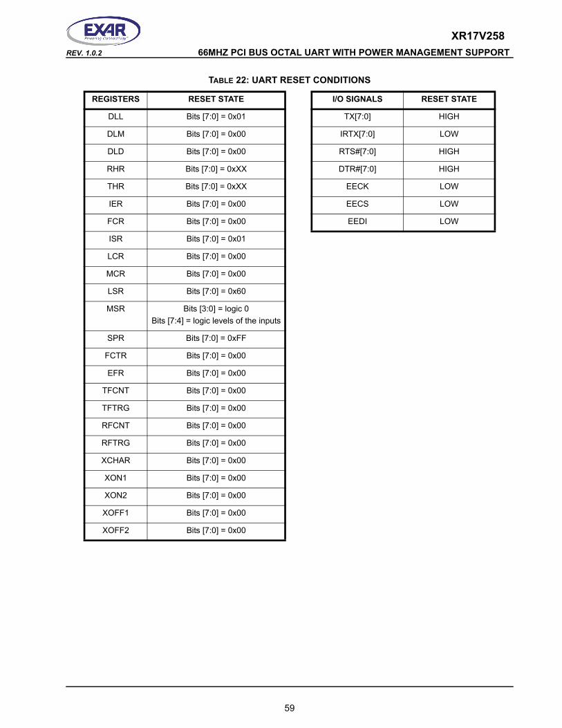
XR17V258REV. 1.0.2 66MHZ PCI BUS OCTAL UART WITH POWER MANAGEMENT SUPPORT
TABLE 22: UART RESET CONDITIONS
DLL Bits [7:0] = 0x01 TX[7:0] HIGH
DLM Bits [7:0] = 0x00 IRTX[7:0] LOW
DLD Bits [7:0] = 0x00 RTS#[7:0] HIGH
RHR Bits [7:0] = 0xXX DTR#[7:0] HIGH
THR Bits [7:0] = 0xXX EECK LOW
IER Bits [7:0] = 0x00 EECS LOW
FCR Bits [7:0] = 0x00 EEDI LOW
ISR Bits [7:0] = 0x01
LCR Bits [7:0] = 0x00
MCR Bits [7:0] = 0x00
LSR Bits [7:0] = 0x60
MSR Bits [3:0] = logic 0 Bits [7:4] = logic levels of the inputs
SPR Bits [7:0] = 0xFF
FCTR Bits [7:0] = 0x00
EFR Bits [7:0] = 0x00
TFCNT Bits [7:0] = 0x00
TFTRG Bits [7:0] = 0x00
RFCNT Bits [7:0] = 0x00
RFTRG Bits [7:0] = 0x00
XCHAR Bits [7:0] = 0x00
XON1 Bits [7:0] = 0x00
XON2 Bits [7:0] = 0x00
XOFF1 Bits [7:0] = 0x00
XOFF2 Bits [7:0] = 0x00
REGISTERS RESET STATE I/O SIGNALS RESET STATE
59
XR17V258 66MHZ PCI BUS OCTAL UART WITH POWER MANAGEMENT SUPPORT REV. 1.0.2
ABSOLUTE MAXIMUM RATINGSPower Supply Range 4 Volts
Voltage at Any Pin -0.5 to 4V
Operating Temperature -40o to +85o C
Storage Temperature -65o to +150o C
Package Dissipation 500 mW
Thermal Resistance (20x20x1.4mm 144-LQFP) theta-ja = 42, theta-jc = 8
ELECTRICAL CHARACTERISTICSDC ELECTRICAL CHARACTERISTICS FOR 3.3V SIGNALLING
O TO OC (INDUSTRIAL GRADE) SUPPLY VOLTAGE, VCC = 3.0 - 3.6V
SYMBOL PARAMETER MIN MAXUNIT
SCONDITION NOTES
VIL Input Low Voltage-0.5 0.3VCC V For PCI bus inputs
-0.5 0.8 V For Non-PCI bus inputs
VIH Input High Voltage
0.5VCC VCC + 0.5 V For PCI bus inputs
2.0 6.0 V For Non-PCI bus inputs 5V tolerant inputs
2.0 VCC + 0.5 For external clock (XTAL1) input only
Not 5V tolerant
VOL Output Low Voltage0.1VCC V IOL = 1.5mA PCI bus outputs
0.4 V IOL = 6mA Non-PCI bus outputs
VOH Output High Voltage0.9VCC V IOH = -0.5mA PCI bus outputs
2.4 V IOH = -2mA Non-PCI bus outputs
IIL Input Leakage Current ±10 µA 0 < Vin < VCC
ICL Input Clock Leakage ±10 µA
CIN Input Pin Capacitance 10 pF
CCLK CLK Pin Capacitance 5 12 pF
CIDSEL IDSEL Pin Capacitance 8 pF
IOff PME# input leakage - 1 µA Vo ≤ 3.6V, VCC off or floating
ICC Power Supply Current 4 mA PCI bus CLK and Ext. Clock = 2MHz,
all inputs at VCC or GND and all outputs are
unloaded.
ISLEEP Sleep Current 1 mA All eight UARTs asleep. AD[31:0] at GND, all
inputs at VCC or GND.
TA=-40 +85
60
XR17V258REV. 1.0.2 66MHZ PCI BUS OCTAL UART WITH POWER MANAGEMENT SUPPORT
AC ELECTRICAL CHARACTERISTICS FOR 3.3V SIGNALING O TO+85OC (INDUSTRIAL GRADE) VCC = 3.0 - 3.6V
SYMBOL PARAMETER MIN MAX UNITS NOTES
XTAL1 UART Crystal Oscillator 24 MHz On-chip osc.
ECLK External Clock 64 MHz Max 8Mbps using 8X
IOH(AC, min) Switching Current High, Min -12VCC mA Vout = 0.3VCC
IOH(AC, max) Switching Current High, Max -32VCC mA Vout = 0.7VCC
IOL(AC, min) Switching Current Low, Min 16VCC mA Vout = 0.6VCC
IOL(AC, max) Switching Current Low, Max 38VCC mA Vout = 0.18VCC
ICH High Clamp Current 25+(Vin-VCC-1)/0.015 mA VCC+4 > Vin ≥ VCC+1
ICL Low Clamp Current -25+(Vin+1)/0.015 mA -3 < Vin ≤ -1
SlewR Output Rise Slew Rate 1 4 V/ns 0.3VCC to 0.6VCC
SlewF Output Fall Slew Rate 1 4 V/ns 0.6VCC to 0.3VCC
Tcyc CLK Cycle Time 15 ns PCI bus Clock, CLKup to 66.67MHz
Thigh CLK High Time 6 ns
Tlow CLK Low Time 6 ns
CLK Slew Rate 1.5 4 V/ns
Tval CLK to Signal Valid Delay 2 6 ns Bused and point to point signals
Ton Float to Active Delay 2 ns
Toff Active to Float Delay 14 ns
Tsu Input Setup Time to CLK -bused signals
3 ns
Tsu (ptp) Input Setup Time to CLK -point to point signals
5 ns
Th Input Hold Time from CLK 0 ns
Trst RST# Active Time After Power Stable
1 ms
Trst-clk# RST# Active Time After CLK Stable
100 us
Trst-off Reset Active to output float delay
40 ns
Trhfa RST# HIGH to first Configu-ration access
225 clocks
Trhff RST# HIGH to first FRAME# assertion
5 clocks
RST# Slew Rate 50 mV/ns
TA=-40
61
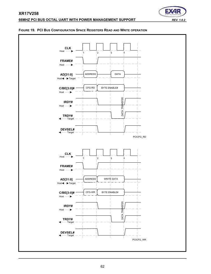
XR17V258 66MHZ PCI BUS OCTAL UART WITH POWER MANAGEMENT SUPPORT REV. 1.0.2
FIGURE 19. PCI BUS CONFIGURATION SPACE REGISTERS READ AND WRITE OPERATION
CLK
FRAME#
AD[31:0]
C/BE[3:0]#
TRDY#
IRDY#
DEVSEL#
1 2 3 4
CFG-RD BYTE ENABLE#
PCICFG_RD
Host
Host
Host
Host
Host Target
Target
Target
DAT
A TR
ANSF
ER
ADDRESS DATA
CLK
FRAME#
AD[31:0]
C/BE[3:0]#
TRDY#
IRDY#
DEVSEL#
1 2 3 4
CFG-WR BYTE ENABLE#
PCICFG_WR
Host
Host
Host
Host
Host Target
Target
Target
DAT
A TR
ANSF
ER
ADDRESS WRITE DATA
62
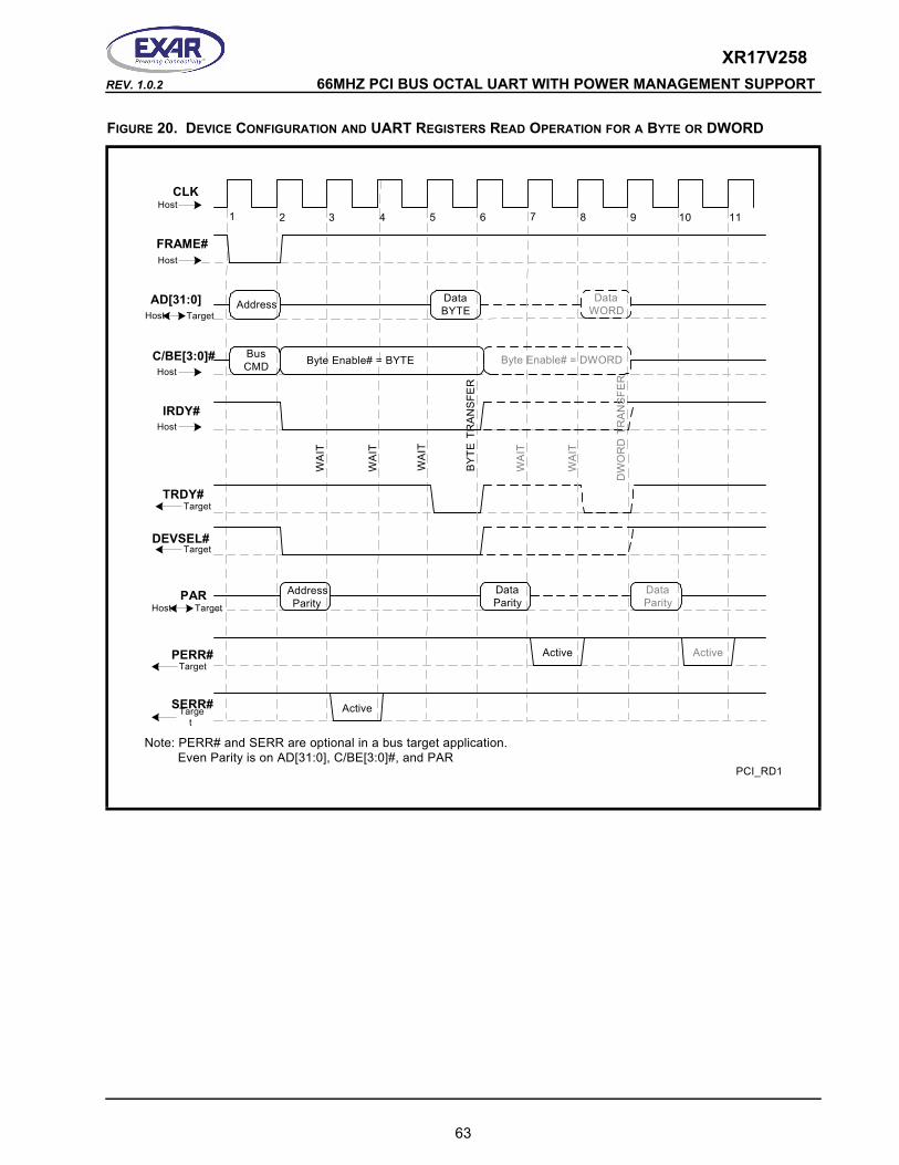
XR17V258REV. 1.0.2 66MHZ PCI BUS OCTAL UART WITH POWER MANAGEMENT SUPPORT
FIGURE 20. DEVICE CONFIGURATION AND UART REGISTERS READ OPERATION FOR A BYTE OR DWORD
CLK
FRAME#
AD[31:0]
C/BE[3:0]#
TRDY#
IRDY#
DEVSEL#
1 2 3 4
Address
BusCMD Byte Enable# = BYTE
BY
TE T
RA
NS
FER
PCI_RD1
5 6 7
PAR
PERR#
8
Note: PERR# and SERR are optional in a bus target application. Even Parity is on AD[31:0], C/BE[3:0]#, and PAR
DataParity
Active
Host
Host
Host
Host
Host Target
Host Target
Target
Target
DataBYTE
WA
IT
WA
IT
WA
IT
AddressParity
SERR#
Target
Target
Active
DataWORD
Byte Enable# = DWORD
DW
OR
D T
RA
NS
FER
WA
IT
WA
ITDataParity
Active
9 10 11
63
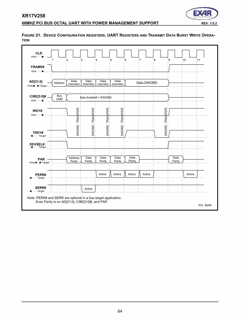
XR17V258 66MHZ PCI BUS OCTAL UART WITH POWER MANAGEMENT SUPPORT REV. 1.0.2
FIGURE 21. DEVICE CONFIGURATION REGISTERS, UART REGISTERS AND TRANSMIT DATA BURST WRITE OPERA-TION
CLK
FRAME#
AD[31:0]
C/BE[3:0]#
TRDY#
IRDY#
DEVSEL#
1 2 3 4
Address
BusCMD Byte Enable# = DWORD
PCI BWR
5 6 7
PAR
PERR#
8
Note: PERR# and SERR are optional in a bus target application. Even Parity is on AD[31:0], C/BE[3:0]#, and PAR
Host
Host
Host
Host
Host Target
Host Target
Target
Target
AddressParity
SERR#
Target
TargetActive
DataParity
Active
9 10
DataDWORD Data DWORD
DW
OR
D
TRA
NS
FER
DW
OR
D
TRA
NS
FER
DW
OR
D
TRA
NS
FER
DW
OR
D
TRA
NS
FER
DW
OR
D
TRA
NS
FER
DataParity
DataParity
DataParity
DataParity
Active Active Active Active
11
DataDWORD
DataDWORD
DataDWORD
64
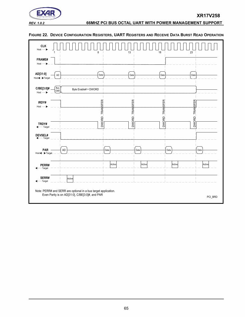
XR17V258REV. 1.0.2 66MHZ PCI BUS OCTAL UART WITH POWER MANAGEMENT SUPPORT
FIGURE 22. DEVICE CONFIGURATION REGISTERS, UART REGISTERS AND RECEIVE DATA BURST READ OPERATION
Data
CLK
FRAME#
AD[31:0]
C/BE[3:0]#
TRDY#
IRDY#
DEVSEL#
1 13
AD
BusCMD Byte Enable# = DWORD
PCI_BRD
PAR
PERR#
18
Note: PERR# and SERR are optional in a bus target application. Even Parity is on AD[31:0], C/BE[3:0]#, and PAR
Host
Host
Host
Host
Host Target
Host Target
Target
Target
SERR#
Target
Target
DW
OR
D
TRA
NS
FER
DW
OR
D
TRA
NS
FER
DW
OR
D
TRA
NS
FER
DW
OR
D
TRA
NS
FER
238
AD Data Data Data Data
Active
Active Active Active Active
Data Data Data
65
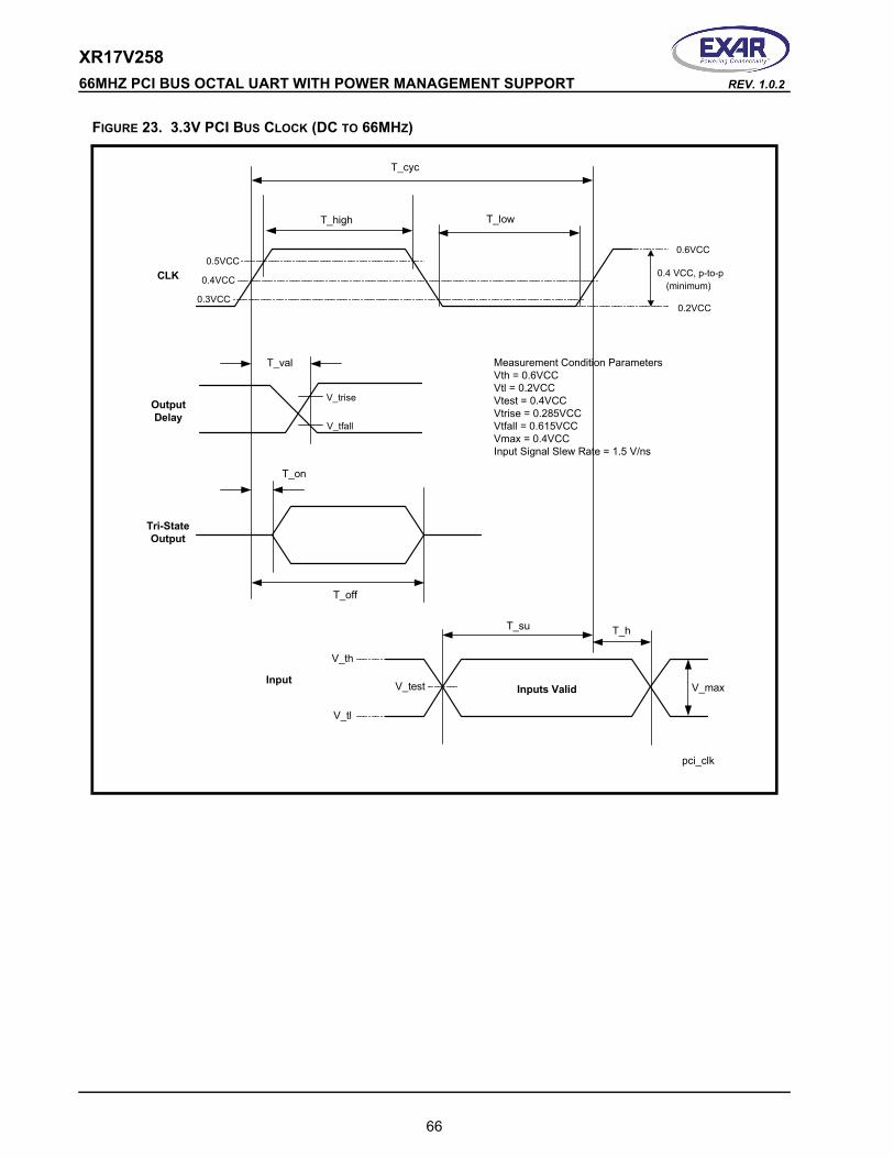
XR17V258 66MHZ PCI BUS OCTAL UART WITH POWER MANAGEMENT SUPPORT REV. 1.0.2
FIGURE 23. 3.3V PCI BUS CLOCK (DC TO 66MHZ)
0.4 VCC, p-to-p(minimum)
0.6VCC
0.2VCC
CLK
OutputDelay
Tri-StateOutput
T_val
T_on
T_off
T_su T_h
pci_clk
Inputs Valid
T_cyc
T_high T_low
0.5VCC
0.4VCC
0.3VCC
V_trise
V_tfall
Input
V_th
V_tl
V_test V_max
Measurement Condition ParametersVth = 0.6VCCVtl = 0.2VCCVtest = 0.4VCCVtrise = 0.285VCCVtfall = 0.615VCCVmax = 0.4VCCInput Signal Slew Rate = 1.5 V/ns
66
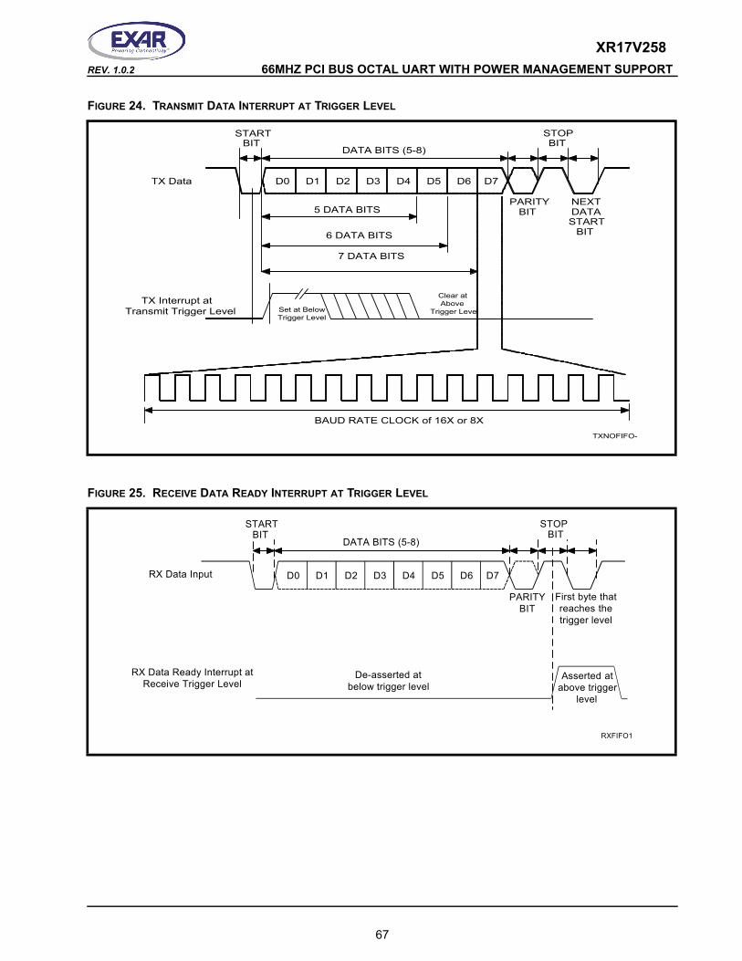
XR17V258REV. 1.0.2 66MHZ PCI BUS OCTAL UART WITH POWER MANAGEMENT SUPPORT
FIGURE 24. TRANSMIT DATA INTERRUPT AT TRIGGER LEVEL
STOPBIT
PARITYBIT
DATA BITS (5-8)
D0 D1 D2 D3 D4 D5 D6 D7
5 DATA BITS
6 DATA BITS
7 DATA BITS
STARTBIT
TX Data
NEXTDATASTART
BIT
TX Interrupt atTransmit Trigger Level
BAUD RATE CLOCK of 16X or 8XTXNOFIFO-1
Set at BelowTrigger Level
Clear atAbove
Trigger Level
FIGURE 25. RECEIVE DATA READY INTERRUPT AT TRIGGER LEVEL
STOPBIT
PARITYBIT
DATA BITS (5-8)
D0 D1 D2 D3 D4 D5 D6 D7
STARTBIT
RX Data Input
First byte thatreaches thetrigger level
RX Data Ready Interrupt atReceive Trigger Level
RXFIFO1
De-asserted atbelow trigger level
Asserted atabove trigger
level
67
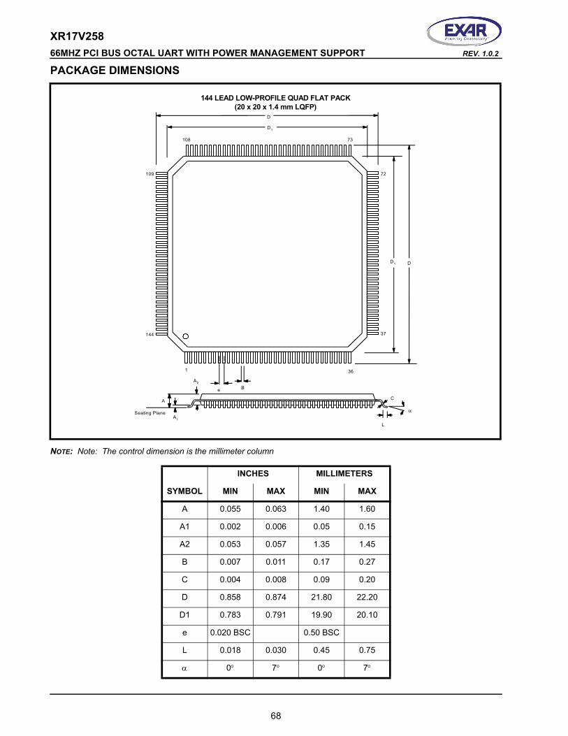
XR17V258 66MHZ PCI BUS OCTAL UART WITH POWER MANAGEMENT SUPPORT REV. 1.0.2
PACKAGE DIMENSIONS
A2
α
L
C
e
108 73
72
37
109
144
D
D1
DD1
1 36
B
A1
A
Seating Plane
144 LEAD LOW-PROFILE QUAD FLAT PACK(20 x 20 x 1.4 mm LQFP)
NOTE:
A 0.055 0.063 1.40 1.60
A1 0.002 0.006 0.05 0.15
A2 0.053 0.057 1.35 1.45
B 0.007 0.011 0.17 0.27
C 0.004 0.008 0.09 0.20
D 0.858 0.874 21.80 22.20
D1 0.783 0.791 19.90 20.10
e 0.020 BSC 0.50 BSC
L 0.018 0.030 0.45 0.75
α 0° 7° 0° 7°
Note: The control dimension is the millimeter column
INCHES MILLIMETERS
SYMBOL MIN MAX MIN MAX
68
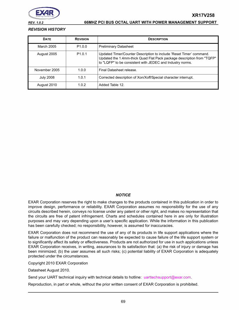
XR17V258REV. 1.0.2 66MHZ PCI BUS OCTAL UART WITH POWER MANAGEMENT SUPPORT
REVISION HISTORY
DATE REVISION DESCRIPTION
March 2005 P1.0.0 Preliminary Datasheet
August 2005 P1.0.1 Updated Timer/Counter Description to include ’Reset Timer’ command. Updated the 1.4mm-thick Quad Flat Pack package description from "TQFP" to "LQFP" to be consistent with JEDEC and Industry norms.
November 2005 1.0.0 Final Datasheet release.
July 2008 1.0.1 Corrected description of Xon/Xoff/Special character interrupt.
August 2010 1.0.2 Added Table 12.
69
NOTICE
EXAR Corporation reserves the right to make changes to the products contained in this publication in order to improve design, performance or reliability. EXAR Corporation assumes no responsibility for the use of any circuits described herein, conveys no license under any patent or other right, and makes no representation that the circuits are free of patent infringement. Charts and schedules contained here in are only for illustration purposes and may vary depending upon a user’s specific application. While the information in this publication has been carefully checked; no responsibility, however, is assumed for inaccuracies.
EXAR Corporation does not recommend the use of any of its products in life support applications where the failure or malfunction of the product can reasonably be expected to cause failure of the life support system or to significantly affect its safety or effectiveness. Products are not authorized for use in such applications unless EXAR Corporation receives, in writing, assurances to its satisfaction that: (a) the risk of injury or damage has been minimized; (b) the user assumes all such risks; (c) potential liability of EXAR Corporation is adequately protected under the circumstances.
Copyright 2010 EXAR Corporation
Datasheet August 2010.
Send your UART technical inquiry with technical details to hotline: [email protected].
Reproduction, in part or whole, without the prior written consent of EXAR Corporation is prohibited.
Related Documents