XAPP1200 (v1.0) March 10, 2014 www.xilinx.com 1 © Copyright 2014 Xilinx, Inc. Xilinx, the Xilinx logo, Artix, ISE, Kintex, Spartan, Virtex, Vivado, Zynq, and other designated brands included herein are trademarks of Xilinx in the United States and other countries. All other trademarks are the property of their respective owners. Summary This application note uses the KC705 Evaluation Kit and the GTX Transceiver Wizard to demonstrate a transceiver example design running on Kintex®-7 FPGA hardware. The KC705 evaluation kit provides a comprehensive, high-performance development and demonstration platform using the Kintex-7 FPGA family for high-bandwidth and high-performance applications in multiple market segments. For more information about this evaluation board, refer to the KC705 Evaluation Board for the Kintex-7 FPGA (UG810) [Ref 1]. Setup Requirements Before you start this tutorial, make sure you have the hardware and software components needed to perform the steps. The required components are listed in this section. • Software: Vivado® Design Suite 2013.3 • Hardware: Kintex-7 FPGA KC705 evaluation board (Figure 1). Hardware Requirements Single-Lane Design • Two Kintex-7 FPGA KC705 evaluation boards • Two universal 12V, 5A power adapters • Two suitable clock generators to generate 156.25 MHz • Two JTAG platform USB cables Application Note: Kintex-7 FPGAs XAPP1200 (v1.0) March 10, 2014 Kintex-7 FPGA Transceiver Wizard Example Design Author: Dinesh Kumar and Thupalli Ramachandra X-Ref Target - Figure 1 Figure 1: KC705 Evaluation Board

Welcome message from author
This document is posted to help you gain knowledge. Please leave a comment to let me know what you think about it! Share it to your friends and learn new things together.
Transcript

XAPP1200 (v1.0) March 10, 2014 www.xilinx.com 1
© Copyright 2014 Xilinx, Inc. Xilinx, the Xilinx logo, Artix, ISE, Kintex, Spartan, Virtex, Vivado, Zynq, and other designated brands included herein are trademarks of Xilinx in the United States and other countries. All other trademarks are the property of their respective owners.
Summary This application note uses the KC705 Evaluation Kit and the GTX Transceiver Wizard to demonstrate a transceiver example design running on Kintex®-7 FPGA hardware. The KC705 evaluation kit provides a comprehensive, high-performance development and demonstration platform using the Kintex-7 FPGA family for high-bandwidth and high-performance applications in multiple market segments. For more information about this evaluation board, refer to the KC705 Evaluation Board for the Kintex-7 FPGA (UG810) [Ref 1].
Setup Requirements
Before you start this tutorial, make sure you have the hardware and software components needed to perform the steps. The required components are listed in this section.
• Software: Vivado® Design Suite 2013.3
• Hardware: Kintex-7 FPGA KC705 evaluation board (Figure 1).
Hardware Requirements
Single-Lane Design• Two Kintex-7 FPGA KC705 evaluation boards
• Two universal 12V, 5A power adapters
• Two suitable clock generators to generate 156.25 MHz
• Two JTAG platform USB cables
Application Note: Kintex-7 FPGAs
XAPP1200 (v1.0) March 10, 2014
Kintex-7 FPGA Transceiver Wizard Example DesignAuthor: Dinesh Kumar and Thupalli Ramachandra
X-Ref Target - Figure 1
Figure 1: KC705 Evaluation Board

Steps to Create Serial Transceivers Using Vivado IDE
XAPP1200 (v1.0) March 10, 2014 www.xilinx.com 2
• Eight SMA-to-SMA connector cables
Four-Lane Design With Internal Loopback• One Kintex-7 FPGA KC705 evaluation board
• One universal 12V, 5A power adapter
• Suitable clock generator to generate 156.25 MHz
• One JTAG platform USB cable
• Two SMA-to-SMA connector cables
Steps to Create Serial Transceivers Using Vivado IDE
To customize and generate a transceiver core and example design using the Vivado IP catalog, follow the steps listed here. This entire document is only tested for 10GBASE-R protocol for demonstration purposes.The same wizard wrapper steps should work for the standard protocols available from the protocol drop-down menu.
1. Open Vivado Design Suite.
2. Select Create New Project and click Next.
3. Select the project name/path and click Next.
4. Select RTL Project to permit running the example design and click Do not specify sources at this time. Click Next.
5. Click xc7k325tffg900-2 or, select the Boards option and then click Kintex-7 FPGA KC705 Evaluation platform.
6. Click Next, then click Finish.
Steps to Create Serial Transceivers Using Vivado IDE
XAPP1200 (v1.0) March 10, 2014 www.xilinx.com 3
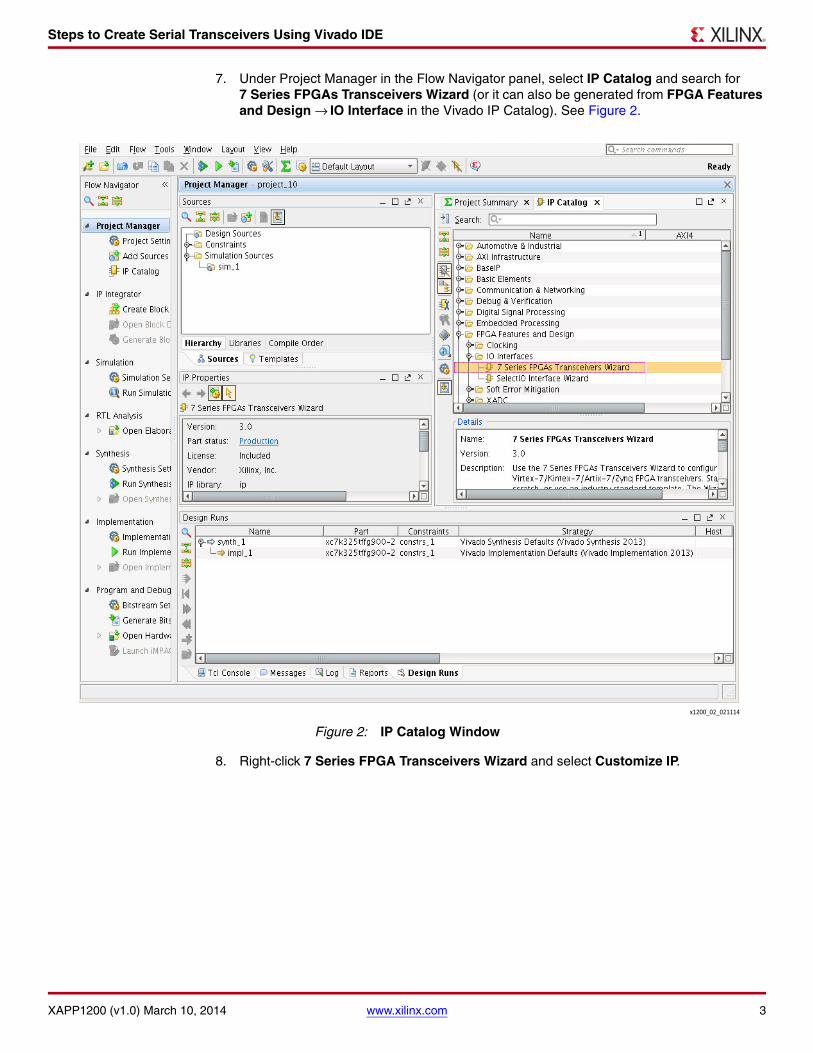
7. Under Project Manager in the Flow Navigator panel, select IP Catalog and search for 7 Series FPGAs Transceivers Wizard (or it can also be generated from FPGA Features and Design → IO Interface in the Vivado IP Catalog). See Figure 2.
8. Right-click 7 Series FPGA Transceivers Wizard and select Customize IP.
X-Ref Target - Figure 2
Figure 2: IP Catalog Window
Steps to Create Serial Transceivers Using Vivado IDE
XAPP1200 (v1.0) March 10, 2014 www.xilinx.com 4
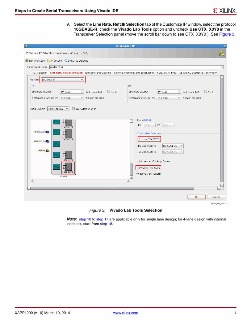
9. Select the Line Rate, Refclk Selection tab of the Customize IP window, select the protocol 10GBASE-R, check the Vivado Lab Tools option and uncheck Use GTX_X0Y0 in the Transceiver Selection panel (move the scroll bar down to see GTX_X0Y0 ). See Figure 3.
Note: step 10 to step 17 are applicable only for single lane design; for 4-lane design with internal loopback, start from step 18.
X-Ref Target - Figure 3
Figure 3: Vivado Lab Tools Selection
Steps to Create Serial Transceivers Using Vivado IDE
XAPP1200 (v1.0) March 10, 2014 www.xilinx.com 5
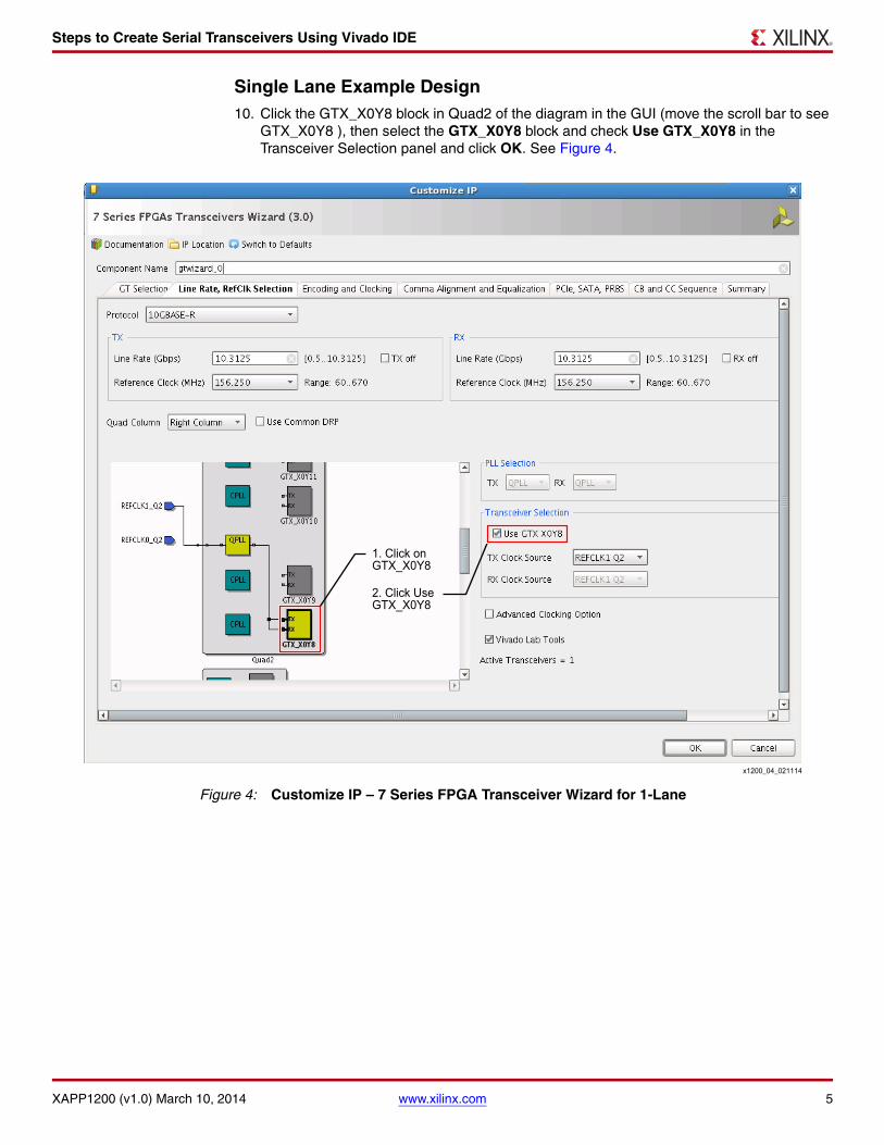
Single Lane Example Design10. Click the GTX_X0Y8 block in Quad2 of the diagram in the GUI (move the scroll bar to see
GTX_X0Y8 ), then select the GTX_X0Y8 block and check Use GTX_X0Y8 in the Transceiver Selection panel and click OK. See Figure 4.
X-Ref Target - Figure 4
Figure 4: Customize IP – 7 Series FPGA Transceiver Wizard for 1-Lane
Steps to Create Serial Transceivers Using Vivado IDE
XAPP1200 (v1.0) March 10, 2014 www.xilinx.com 6
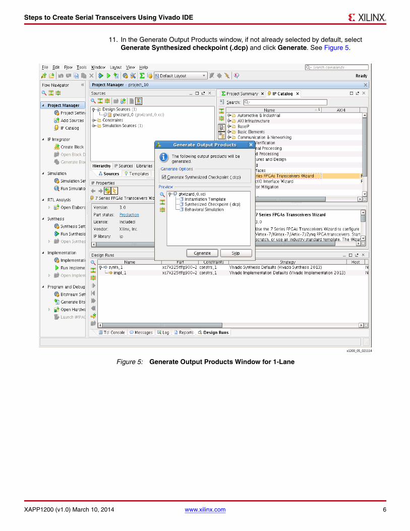
11. In the Generate Output Products window, if not already selected by default, select Generate Synthesized checkpoint (.dcp) and click Generate. See Figure 5.
X-Ref Target - Figure 5
Figure 5: Generate Output Products Window for 1-Lane
Steps to Create Serial Transceivers Using Vivado IDE
XAPP1200 (v1.0) March 10, 2014 www.xilinx.com 7
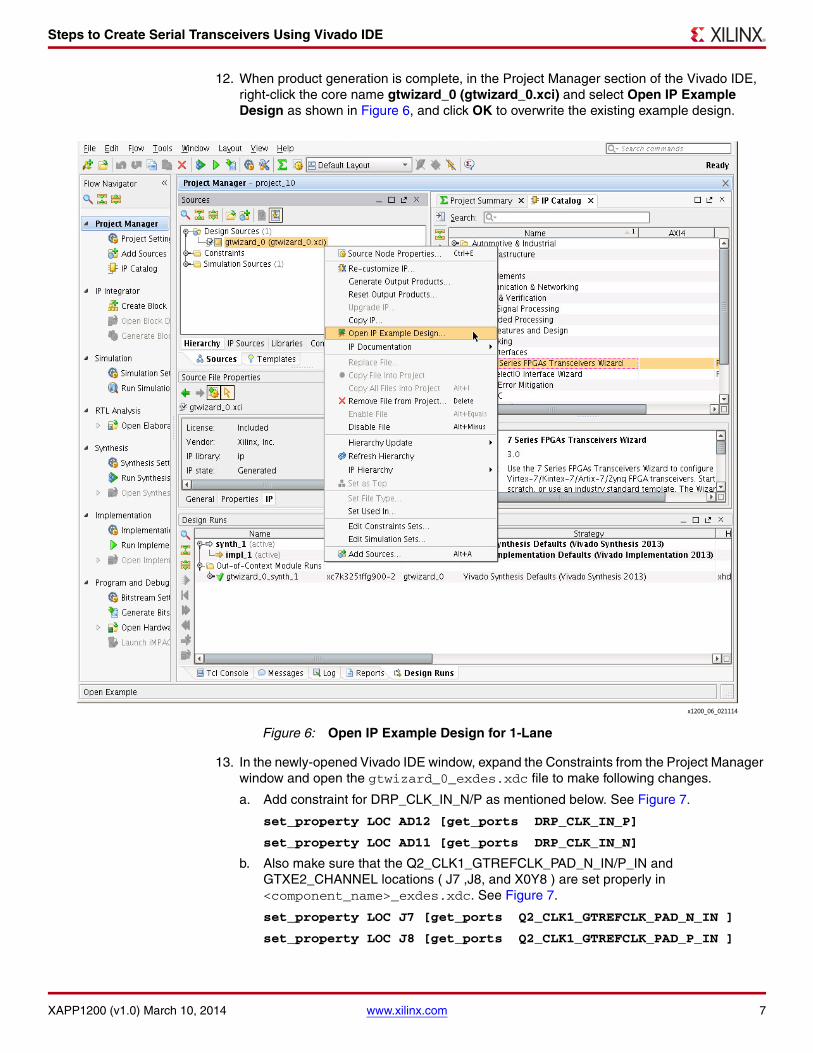
12. When product generation is complete, in the Project Manager section of the Vivado IDE, right-click the core name gtwizard_0 (gtwizard_0.xci) and select Open IP Example Design as shown in Figure 6, and click OK to overwrite the existing example design.
13. In the newly-opened Vivado IDE window, expand the Constraints from the Project Manager window and open the gtwizard_0_exdes.xdc file to make following changes.
a. Add constraint for DRP_CLK_IN_N/P as mentioned below. See Figure 7.
set_property LOC AD12 [get_ports DRP_CLK_IN_P]
set_property LOC AD11 [get_ports DRP_CLK_IN_N]
b. Also make sure that the Q2_CLK1_GTREFCLK_PAD_N_IN/P_IN and GTXE2_CHANNEL locations ( J7 ,J8, and X0Y8 ) are set properly in <component_name>_exdes.xdc. See Figure 7.
set_property LOC J7 [get_ports Q2_CLK1_GTREFCLK_PAD_N_IN ]
set_property LOC J8 [get_ports Q2_CLK1_GTREFCLK_PAD_P_IN ]
X-Ref Target - Figure 6
Figure 6: Open IP Example Design for 1-Lane
Steps to Create Serial Transceivers Using Vivado IDE
XAPP1200 (v1.0) March 10, 2014 www.xilinx.com 8
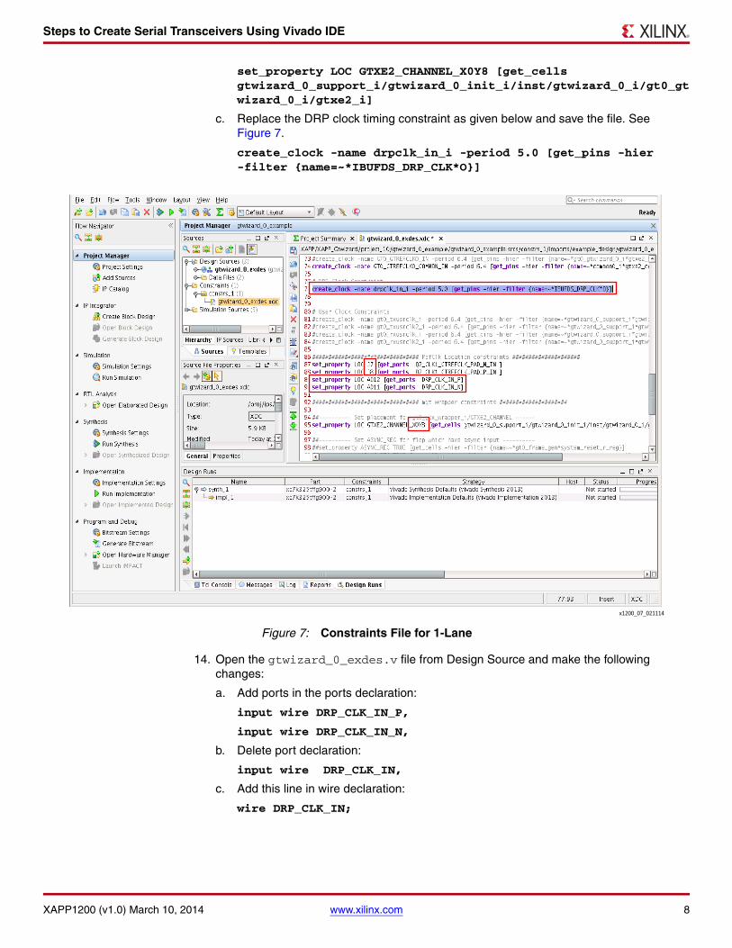
set_property LOC GTXE2_CHANNEL_X0Y8 [get_cells gtwizard_0_support_i/gtwizard_0_init_i/inst/gtwizard_0_i/gt0_gtwizard_0_i/gtxe2_i]
c. Replace the DRP clock timing constraint as given below and save the file. See Figure 7.
create_clock -name drpclk_in_i -period 5.0 [get_pins -hier -filter {name=~*IBUFDS_DRP_CLK*O}]
14. Open the gtwizard_0_exdes.v file from Design Source and make the following changes:
a. Add ports in the ports declaration:
input wire DRP_CLK_IN_P,
input wire DRP_CLK_IN_N,
b. Delete port declaration:
input wire DRP_CLK_IN,
c. Add this line in wire declaration:
wire DRP_CLK_IN;
X-Ref Target - Figure 7
Figure 7: Constraints File for 1-Lane

Steps to Create Serial Transceivers Using Vivado IDE
XAPP1200 (v1.0) March 10, 2014 www.xilinx.com 9
d. Add this module instantiation:
IBUFDS IBUFDS_DRP_CLK
(
.I (DRP_CLK_IN_P),
.IB (DRP_CLK_IN_N),
.O (DRP_CLK_IN)
);
e. Search for wire track_data_out_i and change it to (* mark_debug = "TRUE" *) wire track_data_out_i;
f. Search for probe_in0(tied_to_ground_i) and change it to probe_in0(gt0_rxfsmresetdone_i) and save the file.
15. Now click Run Synthesis, and after synthesis is completed, click Open Synthesized Design. It will run for some time to synthesize and open the synthesized netlist window. Once the synthesized design is opened, continue to step 16.
16. Run write_debug_probes <ltx_file_name> in the Tcl console and press Enter. This will create <ltx_file_name>.ltx under the <component_name>_example folder.
17. Click Run Implementation, and after implementation is completed, click Open Implemented Design. Click Yes in the dialog box to open the implemented design. Vivado IDE will open the implemented design netlist window. Enter the following two Tcl comments in the Tcl console, which will generate the routed.bit bitstream file.
set_property SEVERITY {Warning} [get_drc_checks NSTD-1]; set_property SEVERITY {Warning} [get_drc_checks UCIO-1]write_bitstream -bitgen_options {-g UnconstrainedPins:Allow} -file routed.bit -force
Steps to Create Serial Transceivers Using Vivado IDE
XAPP1200 (v1.0) March 10, 2014 www.xilinx.com 10
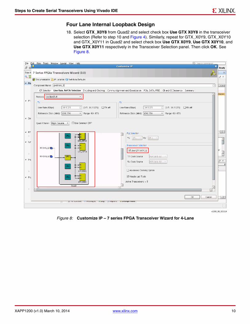
Four Lane Internal Loopback Design18. Select GTX_X0Y8 from Quad2 and select check box Use GTX X0Y8 in the transceiver
selection (Refer to step 10 and Figure 4). Similarly, repeat for GTX_X0Y9, GTX_X0Y10 and GTX_X0Y11 in Quad2 and select check box Use GTX X0Y9, Use GTX X0Y10, and Use GTX X0Y11 respectively in the Transceiver Selection panel. Then click OK. See Figure 8.
X-Ref Target - Figure 8
Figure 8: Customize IP – 7 series FPGA Transceiver Wizard for 4-Lane

Steps to Create Serial Transceivers Using Vivado IDE
XAPP1200 (v1.0) March 10, 2014 www.xilinx.com 11
19. In the Generate Output Products window, if not already selected by default, select Generate Synthesized Checkpoint (.dcp) and click Generate. See Figure 9.
X-Ref Target - Figure 9
Figure 9: Generate Output Products Window for 4-Lane

Steps to Create Serial Transceivers Using Vivado IDE
XAPP1200 (v1.0) March 10, 2014 www.xilinx.com 12
20. When product generation is complete, in the Project Manager section of the Vivado IDE, right-click the core name gtwizard_0 (gtwizard_0.xci), select Open IP Example Design as shown in Figure 10, and click OK to overwrite the existing example design.
21. In the newly-opened Vivado IDE window, expand the Constraints from the Project Manager window and open the gtwizard_0_exdes.xdc file to make following changes.
a. Add constraints for DRP_CLK_IN_N/P as mentioned below. See Figure 11.
set_property LOC AD12 [get_ports DRP_CLK_IN_P]
set_property LOC AD11 [get_ports DRP_CLK_IN_N]
b. Also make sure that the Q2_CLK1_GTREFCLK_PAD_N_IN/P_IN and GTXE2_CHANNEL locations (J7 , J8 , X0Y8 , X0Y9 , X0Y10, and X0Y11 )are set properly in <component_name>_exdes.xdc. See Figure 11.
set_property LOC J7 [get_ports Q2_CLK1_GTREFCLK_PAD_N_IN ]
set_property LOC J8 [get_ports Q2_CLK1_GTREFCLK_PAD_P_IN ]
set_property LOC GTXE2_CHANNEL_X0Y8 [get_cells gtwizard_0_support_i/gtwizard_0_init_i/inst/gtwizard_0_i/gt0_gtwizard_0_i/gtxe2_i]
set_property LOC GTXE2_CHANNEL_X0Y9 [get_cells gtwizard_0_support_i/gtwizard_0_init_i/inst/gtwizard_0_i/gt1_gtwizard_0_i/gtxe2_i]
X-Ref Target - Figure 10
Figure 10: Open IP Example Design for 4-Lane

Steps to Create Serial Transceivers Using Vivado IDE
XAPP1200 (v1.0) March 10, 2014 www.xilinx.com 13
set_property LOC GTXE2_CHANNEL_X0Y10 [get_cells gtwizard_0_support_i/gtwizard_0_init_i/inst/gtwizard_0_i/gt2_gtwizard_0_i/gtxe2_i]
set_property LOC GTXE2_CHANNEL_X0Y11 [get_cells gtwizard_0_support_i/gtwizard_0_init_i/inst/gtwizard_0_i/gt3_gtwizard_0_i/gtxe2_i]
c. Change the DRP clock timing constraint as given below and save the file. See Figure 11.
create_clock -name drpclk_in_i -period 5.0 [get_pins -hier -filter {name=~*IBUFDS_DRP_CLK*O}]
22. Open the gtwizard_0_exdes.v file from Design Source and make the following changes:
a. Add these ports in the ports declaration:
input wire DRP_CLK_IN_P,
input wire DRP_CLK_IN_N,
b. Delete this port declaration:
input wire DRP_CLK_IN,
c. Add these lines in the wire declaration:
X-Ref Target - Figure 11
Figure 11: Constraints File for 4-Lane

Steps to Create Serial Transceivers Using Vivado IDE
XAPP1200 (v1.0) March 10, 2014 www.xilinx.com 14
wire DRP_CLK_IN;
wire rxfsmresetdone;
d. Add this module instantiation to convert the board differential clock to single ended clock using IBUFDS:
IBUFDS IBUFDS_DRP_CLK
(
.I (DRP_CLK_IN_P),
.IB (DRP_CLK_IN_N),
.O (DRP_CLK_IN)
);
assign rxfsmresetdone = (gt0_rxfsmresetdone_i & gt1_rxfsmresetdone_i & gt2_rxfsmresetdone_i & gt3_rxfsmresetdone_i);
e. Search for wire track_data_out_i and change the line to(* mark_debug = "TRUE" *) wire track_data_out_i;
f. Change all the loopback port input values as stated below for internal loopback testing. This enables Near-End PMA loopback testing.
i. (gt0_loopback_i) to (3'b010)
ii. (gt1_loopback_i) to (3'b010)
iii. (gt2_loopback_i) to (3'b010)
iv. (gt3_loopback_i) to (3'b010)
g. Search for probe_in0(tied_to_ground_i) and change to probe_in0(gt0_rxfsmresetdone_i) and save the file.
23. Now click Run Synthesis and once synthesis is completed, click Open Synthesized Design. The program will run for some time to synthesize and open the synthesized netlist window. Once the synthesized design is opened, enter write_debug_probes <ltx_file_name> in the Tcl console and press Enter. This will create <ltx_file_name>.ltx under the <component_name>_example folder.
24. Click Run Implementation and once implementation is completed, click Open Implemented Design. Click Yes in the dialog box to open the implemented design. Vivado IDE will open the implemented design netlist window. Enter the following two Tcl comments in the Tcl console, which will generate the routed.bit bitstream file.
set_property SEVERITY {Warning} [get_drc_checks NSTD-1]; set_property SEVERITY {Warning} [get_drc_checks UCIO-1]
write_bitstream -bitgen_options {-g UnconstrainedPins:Allow} -file routed.bit -force
Steps to Create Serial Transceivers Using Vivado IDE
XAPP1200 (v1.0) March 10, 2014 www.xilinx.com 15
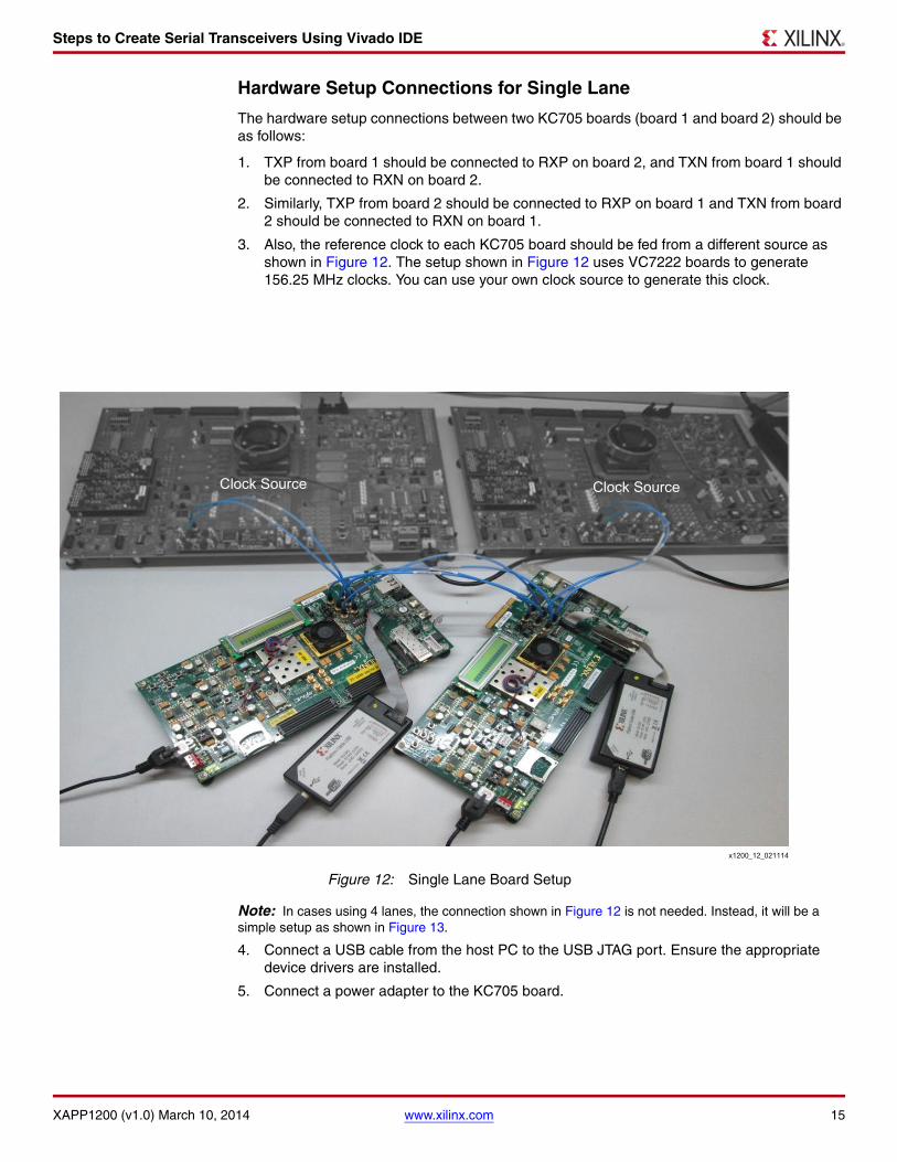
Hardware Setup Connections for Single Lane
The hardware setup connections between two KC705 boards (board 1 and board 2) should be as follows:
1. TXP from board 1 should be connected to RXP on board 2, and TXN from board 1 should be connected to RXN on board 2.
2. Similarly, TXP from board 2 should be connected to RXP on board 1 and TXN from board 2 should be connected to RXN on board 1.
3. Also, the reference clock to each KC705 board should be fed from a different source as shown in Figure 12. The setup shown in Figure 12 uses VC7222 boards to generate 156.25 MHz clocks. You can use your own clock source to generate this clock.
Note: In cases using 4 lanes, the connection shown in Figure 12 is not needed. Instead, it will be a simple setup as shown in Figure 13.
4. Connect a USB cable from the host PC to the USB JTAG port. Ensure the appropriate device drivers are installed.
5. Connect a power adapter to the KC705 board.
X-Ref Target - Figure 12
Figure 12: Single Lane Board Setup

Steps to Create Serial Transceivers Using Vivado IDE
XAPP1200 (v1.0) March 10, 2014 www.xilinx.com 16
Hardware Setup Connections for 4-Lane1. Connect a reference clock from one clock source to the KC705 board, which should be fed
from a different source as shown in Figure 13. You can use your own clock source to generate this clock.
2. Connect a USB cable from the host PC to the USB JTAG port. Ensure the appropriate device drivers are installed.
3. Connect a power adapter to the KC705 board.X-Ref Target - Figure 13
Figure 13: Four Lane Board Setup
Steps to Create Serial Transceivers Using Vivado IDE
XAPP1200 (v1.0) March 10, 2014 www.xilinx.com 17
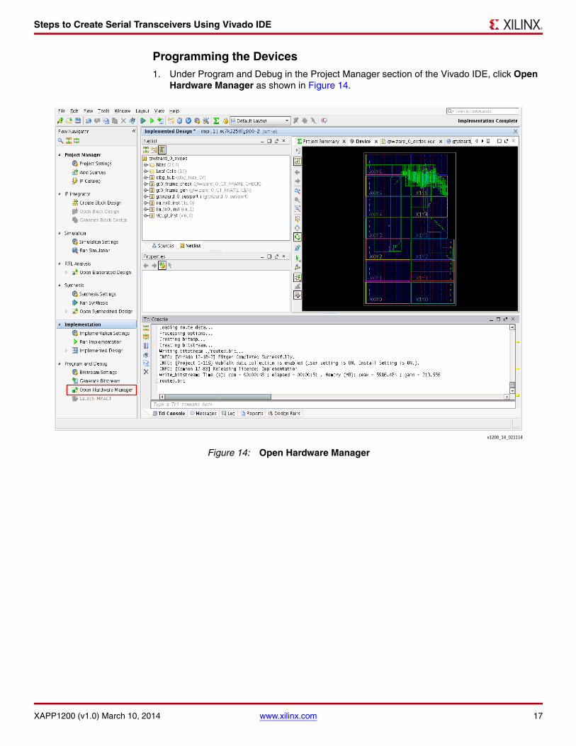
Programming the Devices1. Under Program and Debug in the Project Manager section of the Vivado IDE, click Open
Hardware Manager as shown in Figure 14.X-Ref Target - Figure 14
Figure 14: Open Hardware Manager
Steps to Create Serial Transceivers Using Vivado IDE
XAPP1200 (v1.0) March 10, 2014 www.xilinx.com 18
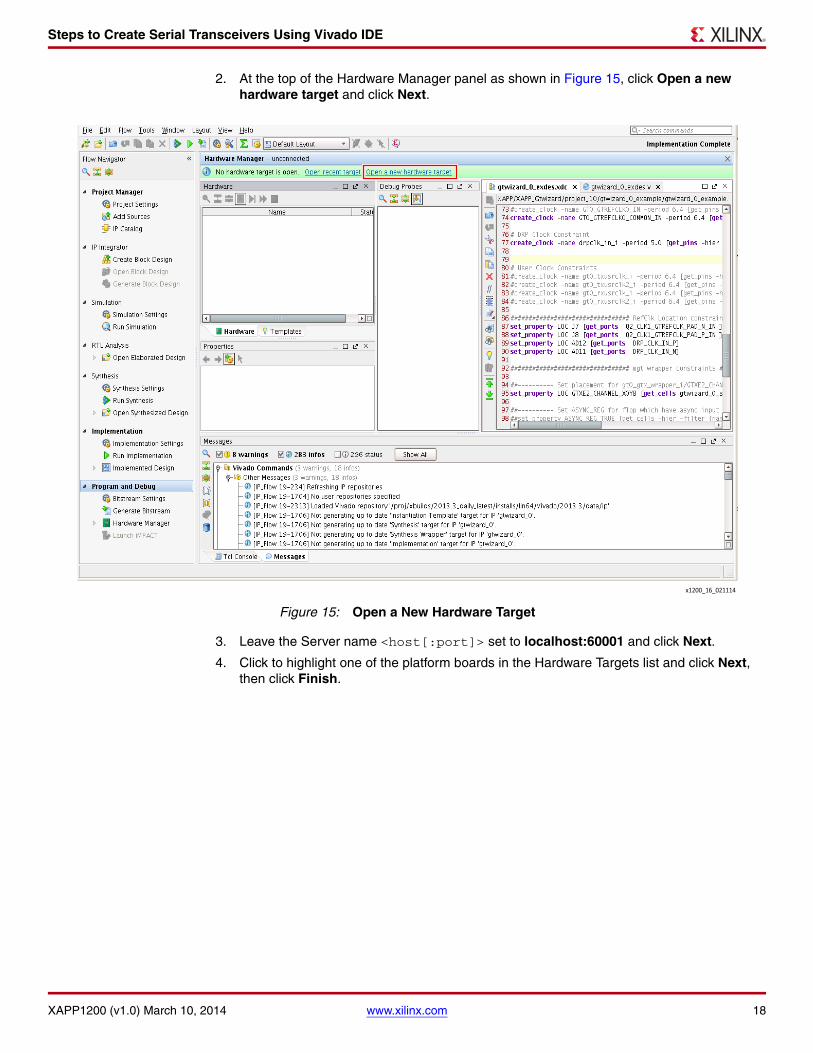
2. At the top of the Hardware Manager panel as shown in Figure 15, click Open a new hardware target and click Next.
3. Leave the Server name <host[:port]> set to localhost:60001 and click Next.
4. Click to highlight one of the platform boards in the Hardware Targets list and click Next, then click Finish.
X-Ref Target - Figure 15
Figure 15: Open a New Hardware Target

Steps to Create Serial Transceivers Using Vivado IDE
XAPP1200 (v1.0) March 10, 2014 www.xilinx.com 19
5. Click Active device XC7K325T_0(0) (Active) in the Hardware list panel. In the Hardware Device Properties dialog box, set Programming file to the bitstream file name (routed.bit) and set Probes file to the probes file name (<ltx_file_name>.ltx) as shown in Figure 16.
6. Right-click the device in the Hardware list and select Program Device... as shown in Figure 17. Ensure that the bitstream file path and name are correct and click OK.
Note: step 7, step 8, and step 9 are not required for 4-lane loopback testing.
X-Ref Target - Figure 16
Figure 16: Hardware Device Properties Panel
X-Ref Target - Figure 17
Figure 17: Program Device

Steps to Create Serial Transceivers Using Vivado IDE
XAPP1200 (v1.0) March 10, 2014 www.xilinx.com 20
7. When programming completes, right-click the programmed target device in the Hardware list and select Close Target as shown in Figure 18.
8. Right-click the second target platform in the Hardware list and select Open Target as shown in Figure 19.
9. Repeat step 5 and step 6 using the same bitstream and probes file names that were used for the first target.
X-Ref Target - Figure 18
Figure 18: Close Target
X-Ref Target - Figure 19
Figure 19: Open Target
Steps to Create Serial Transceivers Using Vivado IDE
XAPP1200 (v1.0) March 10, 2014 www.xilinx.com 21
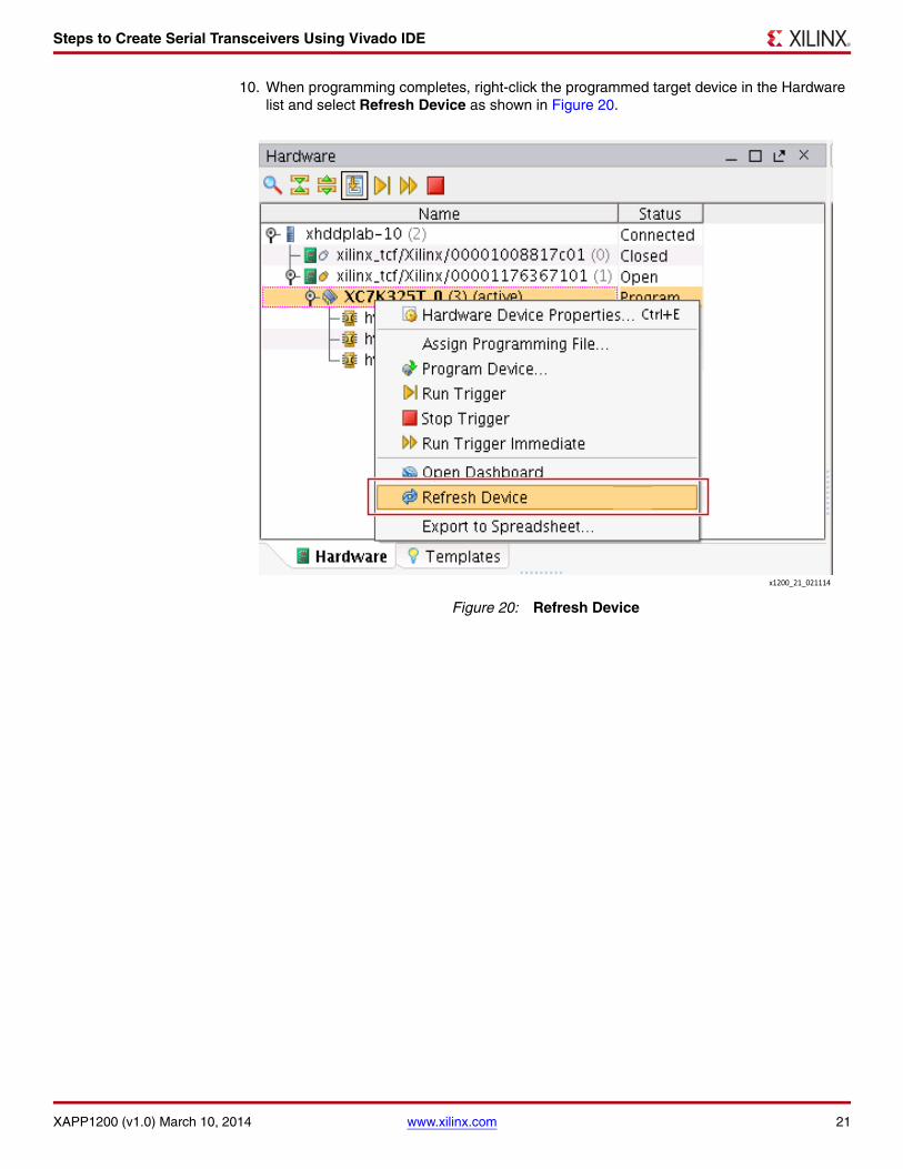
10. When programming completes, right-click the programmed target device in the Hardware list and select Refresh Device as shown in Figure 20.
X-Ref Target - Figure 20
Figure 20: Refresh Device

Steps to Create Serial Transceivers Using Vivado IDE
XAPP1200 (v1.0) March 10, 2014 www.xilinx.com 22
Executing the Design1. Right-click the device in the Hardware list and select Run Trigger, as shown in Figure 21.
You should be able to see all nets which are added in ILA cores.X-Ref Target - Figure 21
Figure 21: Run Trigger

Steps to Create Serial Transceivers Using Vivado IDE
XAPP1200 (v1.0) March 10, 2014 www.xilinx.com 23
2. In the waveform window that appears, observe a High state on the track_data_out_i, gt0_rxreset_done_ila, and gt0_txresetdone_ila signals as shown in Figure 22.
Note: Make sure that the signals have the value as stated below in RX ILA waveform window as shown in Figure 22 Run Trigger.
gt0_rxdata_i[63:0] = some random 64-bit valuegt0_rxreset_done_ila = 1track_data_out_i = 1
X-Ref Target - Figure 22
Figure 22: RX ILA Waveform Window
Steps to Create Serial Transceivers Using Vivado IDE
XAPP1200 (v1.0) March 10, 2014 www.xilinx.com 24
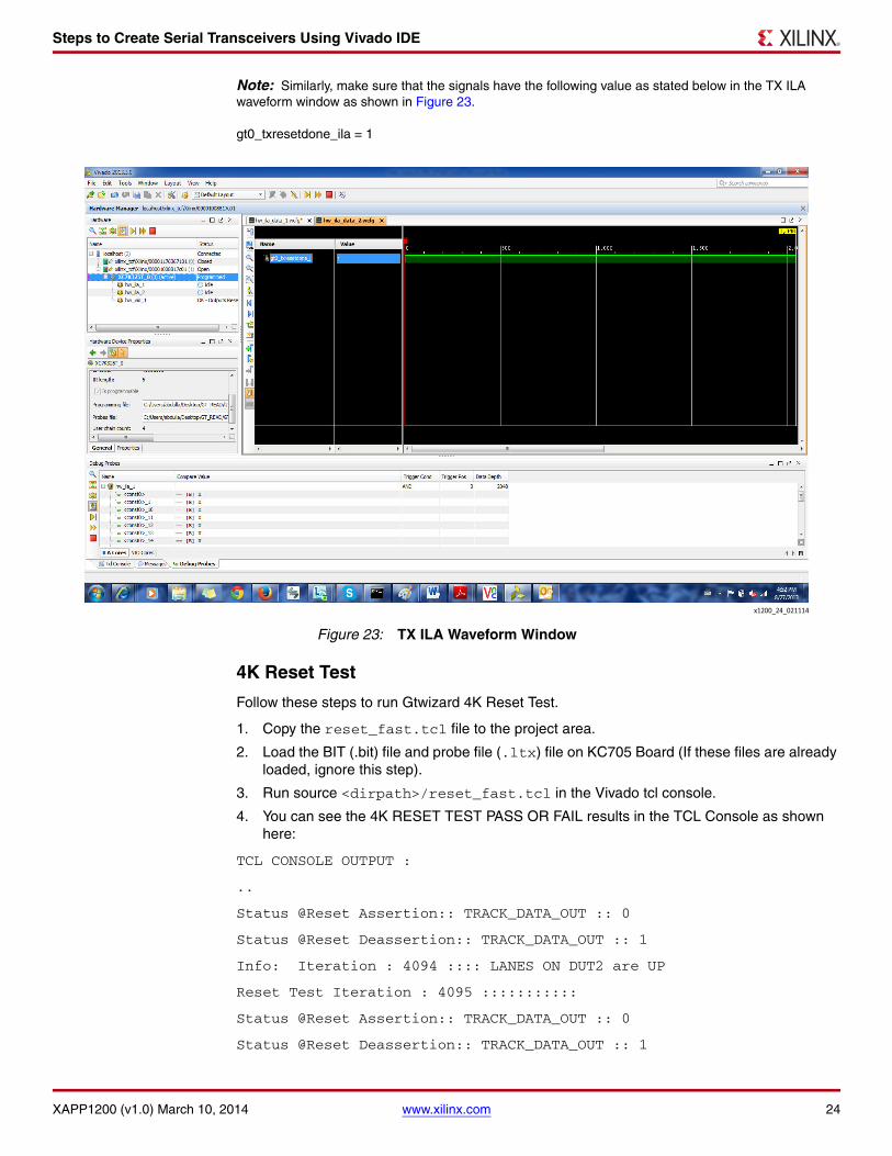
Note: Similarly, make sure that the signals have the following value as stated below in the TX ILA waveform window as shown in Figure 23.
gt0_txresetdone_ila = 1
4K Reset Test
Follow these steps to run Gtwizard 4K Reset Test.
1. Copy the reset_fast.tcl file to the project area.
2. Load the BIT (.bit) file and probe file (.ltx) file on KC705 Board (If these files are already loaded, ignore this step).
3. Run source <dirpath>/reset_fast.tcl in the Vivado tcl console.
4. You can see the 4K RESET TEST PASS OR FAIL results in the TCL Console as shown here:
TCL CONSOLE OUTPUT :
..
Status @Reset Assertion:: TRACK_DATA_OUT :: 0
Status @Reset Deassertion:: TRACK_DATA_OUT :: 1
Info: Iteration : 4094 :::: LANES ON DUT2 are UP
Reset Test Iteration : 4095 :::::::::::
Status @Reset Assertion:: TRACK_DATA_OUT :: 0
Status @Reset Deassertion:: TRACK_DATA_OUT :: 1
X-Ref Target - Figure 23
Figure 23: TX ILA Waveform Window
Reference Design
XAPP1200 (v1.0) March 10, 2014 www.xilinx.com 25
Info: Iteration : 4095 :::: LANES ON DUT2 are UP
Reset Test Iteration : 4096 :::::::::::
Status @Reset Assertion:: TRACK_DATA_OUT :: 0
Status @Reset Deassertion:: TRACK_DATA_OUT :: 1
Info: Iteration : 4096 :::: LANES ON DUT2 are UP
Iteration : 4096 :: TEST PASSED :::::
TCL_OK
Reference Design
The design can be created as per the steps mentioned in this document. The design has been fully verified and tested on hardware.
References This document uses the following references:
1. KC705 Evaluation Board for the Kintex-7 FPGA (UG810)
2. Embedded System Tools Reference Manual: EDK 14.4 (UG111)
3. Vivado design suite 2013.3 User Guide (UG973)
Revision History
The following table shows the revision history for this document.
Table 1: Reference Design Checklist
Parameter Description
General
Developer name Dinesh Kumar, Ramachandra Thupalli
Target devices(stepping level, ES, production, speed grades)
Kintex7 FPGA, KC705 Evaluation Board
Source code provided? Yes
Source code format VHDL/Verilog (some sources encrypted)
Design uses code/IP from existingXilinx application note/reference designs,application note/reference designs,CORE Generator software, or 3rd-party
Reference designs provided usescore generated from Vivado Design Suite 2013.3
Implementation
Synthesis software tools/version used Vivado Design Suite 2013.3
Implementation software tools/versions used Vivado Design Suite 2013.3
Static timing analysis performed? Yes (passing timing in PAR/TRCE)
Hardware Verification
Hardware verified Yes
Hardware platform used for verification KC705 evaluation board
Date Version Description of Revisions
03/102014 1.0 Initial Xilinx release.

Notice of Disclaimer
XAPP1200 (v1.0) March 10, 2014 www.xilinx.com 26
Notice of Disclaimer
The information disclosed to you hereunder (the “Materials”) is provided solely for the selection and use ofXilinx products. To the maximum extent permitted by applicable law: (1) Materials are made available “ASIS” and with all faults, Xilinx hereby DISCLAIMS ALL WARRANTIES AND CONDITIONS, EXPRESS,IMPLIED, OR STATUTORY, INCLUDING BUT NOT LIMITED TO WARRANTIES OFMERCHANTABILITY, NON-INFRINGEMENT, OR FITNESS FOR ANY PARTICULAR PURPOSE; and (2)Xilinx shall not be liable (whether in contract or tort, including negligence, or under any other theory ofliability) for any loss or damage of any kind or nature related to, arising under, or in connection with, theMaterials (including your use of the Materials), including for any direct, indirect, special, incidental, orconsequential loss or damage (including loss of data, profits, goodwill, or any type of loss or damagesuffered as a result of any action brought by a third party) even if such damage or loss was reasonablyforeseeable or Xilinx had been advised of the possibility of the same. Xilinx assumes no obligation tocorrect any errors contained in the Materials or to notify you of updates to the Materials or to productspecifications. You may not reproduce, modify, distribute, or publicly display the Materials without priorwritten consent. Certain products are subject to the terms and conditions of the Limited Warranties whichcan be viewed at http://www.xilinx.com/warranty.htm; IP cores may be subject to warranty and supportterms contained in a license issued to you by Xilinx. Xilinx products are not designed or intended to befail-safe or for use in any application requiring fail-safe performance; you assume sole risk and liability foruse of Xilinx products in Critical Applications: http://www.xilinx.com/warranty.htm#critapps.
Related Documents