DS094 (v3.0) May 20, 2006 www.xilinx.com 1 Product Specification © 2006 Xilinx, Inc. All rights reserved. All Xilinx trademarks, registered trademarks, patents, and disclaimers are as listed at http://www.xilinx.com/legal.htm . All other trademarks and registered trademarks are the property of their respective owners. All specifications are subject to change without notice. Features • Optimized for 1.8V systems - As fast as 5.7 ns pin-to-pin delays - As low as 13 μ A quiescent current • Industry’s best 0.18 micron CMOS CPLD - Optimized architecture for effective logic synthesis. Refer to the CoolRunner™-II family data sheet for architecture description. - Multi-voltage I/O operation — 1.5V to 3.3V • Available in multiple package options - 100-pin VQFP with 80 user I/O - 144-pin TQFP with 118 user I/O - 132-ball CP (0.5mm) BGA with 106 user I/O - 208-pin PQFP with 173 user I/O - 256-ball FT (1.0mm) BGA with 184 user I/O - Pb-free available for all packages • Advanced system features - Fastest in system programming · 1.8V ISP using IEEE 1532 (JTAG) interface - IEEE1149.1 JTAG Boundary Scan Test - Optional Schmitt-trigger input (per pin) - Unsurpassed low power management · DataGATE enable (DGE) signal control - Two separate I/O banks - RealDigital 100% CMOS product term generation - Flexible clocking modes · Optional DualEDGE triggered registers · Clock divider (divide by 2,4,6,8,10,12,14,16) · CoolCLOCK - Global signal options with macrocell control · Multiple global clocks with phase selection per macrocell · Multiple global output enables · Global set/reset - Advanced design security - PLA architecture · Superior pinout retention · 100% product term routability across function block - Open-drain output option for Wired-OR and LED drive - Optional bus-hold, 3-state or weak pull-up on selected I/O pins - Optional configurable grounds on unused I/Os - Mixed I/O voltages compatible with 1.5V, 1.8V, 2.5V, and 3.3V logic levels · SSTL2-1, SSTL3-1, and HSTL-1 I/O compatibility - Hot pluggable Description The CoolRunner™-II 256-macrocell device is designed for both high performance and low power applications. This lends power savings to high-end communication equipment and high speed to battery operated devices. Due to the low power stand-by and dynamic operation, overall system reli- ability is improved This device consists of sixteen Function Blocks inter-con- nected by a low power Advanced Interconnect Matrix (AIM). The AIM feeds 40 true and complement inputs to each Function Block. The Function Blocks consist of a 40 by 56 P-term PLA and 16 macrocells which contain numerous configuration bits that allow for combinational or registered modes of operation. Additionally, these registers can be globally reset or preset and configured as a D or T flip-flop or as a D latch. There are also multiple clock signals, both global and local product term types, configured on a per macrocell basis. Output pin configurations include slew rate limit, bus hold, pull-up, open drain and programmable grounds. A Schmitt-trigger input is available on a per input pin basis. In addition to stor- ing macrocell output states, the macrocell registers may be configured as "direct input" registers to store signals directly from input pins. Clocking is available on a global or Function Block basis. Three global clocks are available for all Function Blocks as a synchronous clock source. Macrocell registers can be individually configured to power up to the zero or one state. A global set/reset control line is also available to asynchro- nously set or reset selected registers during operation. Additional local clock, synchronous clock-enable, asynchro- nous set/reset and output enable signals can be formed using product terms on a per-macrocell or per-Function Block basis. A DualEDGE flip-flop feature is also available on a per mac- rocell basis. This feature allows high performance synchro- nous operation based on lower frequency clocking to help reduce the total power consumption of the device. Circuitry has also been included to divide one externally supplied global clock (GCK2) by eight different selections. This yields divide by even and odd clock frequencies. The use of the clock divide (division by 2) and DualEDGE flip-flop gives the resultant CoolCLOCK feature. DataGATE is a method to selectively disable inputs of the CPLD that are not of interest during certain points in time. 0 XC2C256 CoolRunner-II CPLD DS094 (v3.0) May 20, 2006 0 0 Product Specification R

Welcome message from author
This document is posted to help you gain knowledge. Please leave a comment to let me know what you think about it! Share it to your friends and learn new things together.
Transcript
Featuresbull Optimized for 18V systems
- As fast as 57 ns pin-to-pin delays- As low as 13 μA quiescent current
bull Industryrsquos best 018 micron CMOS CPLD- Optimized architecture for effective logic synthesis
Refer to the CoolRunnertrade-II family data sheet for architecture description
- Multi-voltage IO operation mdash 15V to 33V bull Available in multiple package options
- 100-pin VQFP with 80 user IO- 144-pin TQFP with 118 user IO- 132-ball CP (05mm) BGA with 106 user IO- 208-pin PQFP with 173 user IO- 256-ball FT (10mm) BGA with 184 user IO- Pb-free available for all packages
bull Advanced system features- Fastest in system programming
middot 18V ISP using IEEE 1532 (JTAG) interface- IEEE11491 JTAG Boundary Scan Test- Optional Schmitt-trigger input (per pin)- Unsurpassed low power management
middot DataGATE enable (DGE) signal control- Two separate IO banks- RealDigital 100 CMOS product term generation- Flexible clocking modes
middot Optional DualEDGE triggered registersmiddot Clock divider (divide by 246810121416)middot CoolCLOCK
- Global signal options with macrocell controlmiddot Multiple global clocks with phase selection per
macrocellmiddot Multiple global output enablesmiddot Global setreset
- Advanced design security- PLA architecture
middot Superior pinout retentionmiddot 100 product term routability across function
block- Open-drain output option for Wired-OR and LED
drive- Optional bus-hold 3-state or weak pull-up on
selected IO pins- Optional configurable grounds on unused IOs- Mixed IO voltages compatible with 15V 18V
25V and 33V logic levelsmiddot SSTL2-1 SSTL3-1 and HSTL-1 IO compatibility
- Hot pluggable
DescriptionThe CoolRunnertrade-II 256-macrocell device is designed forboth high performance and low power applications Thislends power savings to high-end communication equipmentand high speed to battery operated devices Due to the lowpower stand-by and dynamic operation overall system reli-ability is improvedThis device consists of sixteen Function Blocks inter-con-nected by a low power Advanced Interconnect Matrix (AIM)The AIM feeds 40 true and complement inputs to eachFunction Block The Function Blocks consist of a 40 by 56P-term PLA and 16 macrocells which contain numerousconfiguration bits that allow for combinational or registeredmodes of operation Additionally these registers can be globally reset or presetand configured as a D or T flip-flop or as a D latch Thereare also multiple clock signals both global and local productterm types configured on a per macrocell basis Output pinconfigurations include slew rate limit bus hold pull-upopen drain and programmable grounds A Schmitt-triggerinput is available on a per input pin basis In addition to stor-ing macrocell output states the macrocell registers may beconfigured as direct input registers to store signals directlyfrom input pins Clocking is available on a global or Function Block basisThree global clocks are available for all Function Blocks asa synchronous clock source Macrocell registers can beindividually configured to power up to the zero or one stateA global setreset control line is also available to asynchro-nously set or reset selected registers during operationAdditional local clock synchronous clock-enable asynchro-nous setreset and output enable signals can be formedusing product terms on a per-macrocell or per-FunctionBlock basis A DualEDGE flip-flop feature is also available on a per mac-rocell basis This feature allows high performance synchro-nous operation based on lower frequency clocking to helpreduce the total power consumption of the deviceCircuitry has also been included to divide one externallysupplied global clock (GCK2) by eight different selectionsThis yields divide by even and odd clock frequenciesThe use of the clock divide (division by 2) and DualEDGEflip-flop gives the resultant CoolCLOCK featureDataGATE is a method to selectively disable inputs of theCPLD that are not of interest during certain points in time
0
XC2C256 CoolRunner-II CPLD
DS094 (v30) May 20 2006 0 0 Product Specification
R
DS094 (v30) May 20 2006 wwwxilinxcom 1Product Specification
copy 2006 Xilinx Inc All rights reserved All Xilinx trademarks registered trademarks patents and disclaimers are as listed at httpwwwxilinxcomlegalhtm All other trademarks and registered trademarks are the property of their respective owners All specifications are subject to change without notice
XC2C256 CoolRunner-II CPLDR
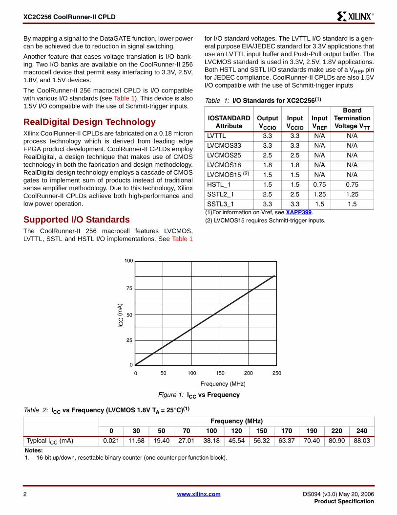
By mapping a signal to the DataGATE function lower powercan be achieved due to reduction in signal switchingAnother feature that eases voltage translation is IO bank-ing Two IO banks are available on the CoolRunner-II 256macrocell device that permit easy interfacing to 33V 25V18V and 15V devicesThe CoolRunner-II 256 macrocell CPLD is IO compatiblewith various IO standards (see Table 1) This device is also15V IO compatible with the use of Schmitt-trigger inputs
RealDigital Design TechnologyXilinx CoolRunner-II CPLDs are fabricated on a 018 micronprocess technology which is derived from leading edgeFPGA product development CoolRunner-II CPLDs employRealDigital a design technique that makes use of CMOStechnology in both the fabrication and design methodologyRealDigital design technology employs a cascade of CMOSgates to implement sum of products instead of traditionalsense amplifier methodology Due to this technology XilinxCoolRunner-II CPLDs achieve both high-performance andlow power operation
Supported IO StandardsThe CoolRunner-II 256 macrocell features LVCMOSLVTTL SSTL and HSTL IO implementations See Table 1
for IO standard voltages The LVTTL IO standard is a gen-eral purpose EIAJEDEC standard for 33V applications thatuse an LVTTL input buffer and Push-Pull output buffer TheLVCMOS standard is used in 33V 25V 18V applicationsBoth HSTL and SSTL IO standards make use of a VREF pinfor JEDEC compliance CoolRunner-II CPLDs are also 15VIO compatible with the use of Schmitt-trigger inputs
Table 1 IO Standards for XC2C256(1)
IOSTANDARD Attribute
Output VCCIO
Input VCCIO
Input VREF
Board TerminationVoltage VTT
LVTTL 33 33 NA NA
LVCMOS33 33 33 NA NA
LVCMOS25 25 25 NA NA
LVCMOS18 18 18 NA NA
LVCMOS15 (2) 15 15 NA NA
HSTL_1 15 15 075 075
SSTL2_1 25 25 125 125
SSTL3_1 33 33 15 15(1)For information on Vref see XAPP399(2) LVCMOS15 requires Schmitt-trigger inputs
Figure 1 ICC vs Frequency
Table 2 ICC vs Frequency (LVCMOS 18V TA = 25degC)(1)
Frequency (MHz)
0 30 50 70 100 120 150 170 190 220 240
Typical ICC (mA) 0021 1168 1940 2701 3818 4554 5632 6337 7040 8090 8803
Notes 1 16-bit updown resettable binary counter (one counter per function block)
Frequency (MHz)
I CC
(m
A)
0
0
25
50
75
100
25020015010050
2 wwwxilinxcom DS094 (v30) May 20 2006Product Specification
XC2C256 CoolRunner-II CPLDR
Recommended Operating Conditions
DC Electrical Characteristics (Over Recommended Operating Conditions)
Absolute Maximum RatingsSymbol Description Value Units
VCC Supply voltage relative to ground ndash05 to 20 V
VCCIO Supply voltage for output drivers ndash05 to 40 V
VJTAG(2) JTAG input voltage limits ndash05 to 40 V
VCCAUX JTAG input supply voltage ndash05 to 40 V
VIN(1) Input voltage relative to ground ndash05 to 40 V
VTS(1) Voltage applied to 3-state output ndash05 to 40 V
TSTG(3) Storage Temperature (ambient) ndash65 to +150 degC
TJ Junction Temperature +150 degC
Notes 1 Maximum DC undershoot below GND must be limited to either 05V or 10 mA whichever is easiest to achieve During transitions
the device pins may undershoot to ndash20v or overshoot to +45V provided this over or undershoot lasts less than 10 ns and with the forcing current being limited to 200 mA
2 Valid over commercial temperature range3 For soldering guidelines and thermal considerations see the Device Packaging information on the Xilinx website For Pb free
packages see XAPP427
Symbol Parameter Min Max Units
VCC Supply voltage for internal logic and input buffers
Commercial TA = 0degC to +70degC 17 19 V
Industrial TA = ndash40degC to +85degC 17 19 V
VCCIO Supply voltage for output drivers 33V operation 30 36 V
Supply voltage for output drivers 25V operation 23 27 V
Supply voltage for output drivers 18V operation 17 19 V
Supply voltage for output drivers 15V operation 14 16 V
VCCAUX JTAG programming 17 36 V
Symbol Parameter Test Conditions Typical Max UnitsICCSB Standby current Commercial VCC = 19V VCCIO = 36V 33 150 μA
ICCSB Standby current Industrial VCC = 19V VCCIO = 36V 54 300 μA
ICC Dynamic current f = 1 MHz - 410 μA
f = 50 MHz - 27 mA
CJTAG JTAG input capacitance f = 1 MHz - 10 pF
CCLK Global clock input capacitance f = 1 MHz - 12 pF
CIO IO capacitance f = 1 MHz - 10 pF
IIL(2) Input leakage current VIN = 0V or VCCIO to 39V - +ndash1 μAIIH(2) IO High-Z leakage VIN = 0V or VCCIO to 39V - +ndash1 μA
Notes 1 16-bit updown resettable binary counter (one counter per function block) tested at VCC= VCCIO = 19V2 See Quality and Reliability section of the CoolRunner-II family data sheet
DS094 (v30) May 20 2006 wwwxilinxcom 3Product Specification
XC2C256 CoolRunner-II CPLDR
LVCMOS 33V and LVTTL 33V DC Voltage Specifications
LVCMOS 25V DC Voltage Specifications
LVCMOS 18V DC Voltage Specifications
LVCMOS 15V DC Voltage Specifications(1)
Symbol Parameter Test Conditions Min Max Units
VCCIO Input source voltage - 30 36 V
VIH High level input voltage - 2 39 V
VIL Low level input voltage - ndash03 08 V
VOH High level output voltage IOH = ndash8 mA VCCIO = 3V VCCIO ndash 04V - V
IOH = ndash01 mA VCCIO = 3V VCCIO ndash 02V - V
VOL Low level output voltage IOL = 8 mA VCCIO = 3V - 04 V
IOL = 01 mA VCCIO = 3V - 02 V
Symbol Parameter Test Conditions Min Max Units
VCCIO Input source voltage - 23 27 V
VIH High level input voltage - 17 39 V
VIL Low level input voltage - ndash03 07 V
VOH High level output voltage IOH = ndash8 mA VCCIO = 23V VCCIO ndash 04V - V
IOH = ndash01 mA VCCIO = 23V VCCIO ndash 02V - V
VOL Low level output voltage IOL = 8 mA VCCIO = 23V - 04 V
IOL = 01 mA VCCIO = 23V - 02 V
Symbol Parameter Test Conditions Min Max Units
VCCIO Input source voltage - 17 19 V
VIH High level input voltage - 065 x VCCIO 39 V
VIL Low level input voltage - ndash03 035 x VCCIO V
VOH High level output voltage IOH = ndash8 mA VCCIO = 17V VCCIO ndash 045 - V
IOH = ndash01 mA VCCIO = 17V VCCIO ndash 02 - V
VOL Low level output voltage IOL = 8 mA VCCIO = 17V - 045 V
IOL = 01 mA VCCIO = 17V - 02 V
Symbol Parameter Test Conditions Min Max UnitsVCCIO Input source voltage - 14 16 V
VT+ Input hysteresis threshold voltage - 05 x VCCIO 08 x VCCIO V
VT- - 02 x VCCIO 05 x VCCIO V
VOH High level output voltage IOH = ndash8 mA VCCIO = 14V VCCIO ndash 045 - V
IOH = ndash01 mA VCCIO = 14V VCCIO ndash 02 - V
4 wwwxilinxcom DS094 (v30) May 20 2006Product Specification
XC2C256 CoolRunner-II CPLDR
Schmitt Trigger Input DC Voltage Specifications
SSTL2-1 DC Voltage Specifications
VOL Low level output voltage IOL = 8 mA VCCIO = 14V - 04 V
IOL = 01 mA VCCIO = 14V - 02 V
Notes 1 Hysteresis used on 15V inputs
Symbol Parameter Test Conditions Min Max UnitsVCCIO Input source voltage - 14 39 V
VT+ Input hysteresis threshold voltage - 05 x VCCIO 08 x VCCIO V
VT- - 02 x VCCIO 05 x VCCIO V
Symbol Parameter Test Conditions Min Typ Max Units
VCCIO Input source voltage - 23 25 27 V
VREF(1) Input reference voltage - 115 125 135 V
VTT(2) Termination voltage - VREF ndash 004 125 VREF + 004 V
VIH High level input voltage - VREF + 018 - 39 V
VIL Low level input voltage - ndash03 - VREF ndash 018 V
VOH High level output voltage IOH = ndash8 mA VCCIO = 23V VCCIO ndash 062 - - V
VOL Low level output voltage IOL = 8 mA VCCIO = 23V - - 054 V
Notes 1 VREF should track the variations in VCCIO also peak to peak AC noise on VREF may not exceed plusmn 2 VREF2 VTT of transmitting device must track VREF of receiving devices
Symbol Parameter Test Conditions Min Max Units
DS094 (v30) May 20 2006 wwwxilinxcom 5Product Specification
XC2C256 CoolRunner-II CPLDR
SSTL3-1 DC Voltage Specifications
HSTL1 DC Voltage Specifications
AC Electrical Characteristics Over Recommended Operating Conditions
Symbol Parameter Test Conditions Min Typ Max Units
VCCIO Input source voltage - 30 33 36 V
VREF(1) Input reference voltage - 13 15 17 V
VTT(2) Termination voltage - VREF ndash 005 15 VREF + 005 V
VIH High level input voltage - VREF + 02 - VCCIO + 03 V
VIL Low level input voltage - ndash03 - VREF ndash 02 V
VOH High level output voltage IOH = ndash8 mA VCCIO = 3V VCCIO ndash 11 - - V
VOL Low level output voltage IOL = 8 mA VCCIO = 3V - - 07 V
Notes 1 VREF should track the variations in VCCIO also peak to peak AC noise on VREF may not exceed plusmn 2 VREF2 VTT of transmitting device must track VREF of receiving devices
Symbol Parameter Test Conditions Min Typ Max Units
VCCIO Input source voltage - 14 15 16 V
VREF(1) Input reference voltage - 068 075 090 V
VTT(2) Termination voltage - - VCCIO x 05 - V
VIH High level input voltage - VREF + 01 - 19 V
VIL Low level input voltage - ndash03 - VREF ndash 01 V
VOH High level output voltage IOH = ndash8 mA VCCIO = 17V VCCIO ndash 04 - - V
VOL Low level output voltage IOL = 8 mA VCCIO = 17V - - 04 V
Notes 1 VREF should track the variations in VCCIO also peak-to-peak AC noise on VREF may not exceed plusmn 2 VREF2 VTT of transmitting device must track VREF of receiving devices
Symbol Parameter
-6 -7
UnitsMin Max Min Max
TPD1 Propagation delay single p-term - 57 - 67 ns
TPD2 Propagation delay OR array - 60 - 75 ns
TSUD Direct input register clock setup time 26 - 30 - ns
TSU1 Setup time (single p-term) 24 - 28 - ns
TSU2 Setup time (OR array) 27 - 33 - ns
THD Direct input register hold time 0 - 0 - ns
TH P-term hold time 0 - 0 - ns
TCO Clock to output - 45 - 60 ns
FTOGGLE(1) Internal toggle rate - 500 - 300 MHz
FSYSTEM1(2) Maximum system frequency - 256 - 152 MHz
FSYSTEM2(2) Maximum system frequency - 238 - 141 MHz
FEXT1(3) Maximum external frequency - 145 - 114 MHz
FEXT2(3) Maximum external frequency - 139 - 108 MHz
TPSUD Direct input register p-term clock setup time 09 - 17 - ns
6 wwwxilinxcom DS094 (v30) May 20 2006Product Specification
XC2C256 CoolRunner-II CPLDR
TPSU1 P-term clock setup time (single p-term) 07 - 15 - ns
TPSU2 P-term clock setup time (OR array) 10 - 20 - ns
TPHD Direct input register p-term clock hold time 09 - 12 - ns
TPH P-term clock hold 07 - 10 - ns
TPCO P-term clock to output - 62 - 73 ns
TOETOD Global OE to output enabledisable - 56 - 70 ns
TPOETPOD P-term OE to output enabledisable - 70 - 80 ns
TMOETMOD Macrocell driven OE to output enabledisable - 74 - 99 ns
TPAO P-term setreset to output valid - 70 - 81 ns
TAO Global setreset to output valid - 55 - 76 ns
TSUEC Register clock enable setup time 25 - 31 - ns
THEC Register clock enable hold time 0 - 0 - ns
TCW Global clock pulse width High or Low 14 - 22 - ns
TPCW P-term pulse width High or Low 60 - 75 - ns
TAPRPW Asynchronous presetreset pulse width (High or Low) 60 - 75 - ns
TDGSU Set-up before DataGATE latch assertion 0 - 0 - ns
TDGH Hold to DataGATE latch assertion 40 - 60 - ns
TDGR DataGATE recovery to new data - 82 - 90 ns
TDGW DataGATE low pulse width 25 - 35 - ns
TCDRSU CDRST setup time before falling edge GCLK2 13 - 20 - ns
TCDRH Hold time CDRST after falling edge GCLK2 0 - 0 - ns
TCONFIG(4) Configuration time - 150 - 150 μs
Notes 1 FTOGGLE is the maximum clock frequency to which a T-Flip Flop can reliably toggle (see the CoolRunner-II family data sheet for more
information)2 FSYSTEM1 (1TCYCLE) is the internal operating frequency for a device fully populated with one 16-bit counter through one p-term per
macrocell while FSYSTEM2 is through the OR array3 FEXT1 (1TSU1+TCO) is the maximum external frequency using one p-term while FEXT2 is through the OR array4 Typical configuration current during TCONFIG is approximately 77 mA
Symbol Parameter
-6 -7
UnitsMin Max Min Max
DS094 (v30) May 20 2006 wwwxilinxcom 7Product Specification
XC2C256 CoolRunner-II CPLDR
(
Internal Timing Parameters
Symbol Parameter(2)
-6 -7
UnitsMin Max Min Max
Buffer Delays
TIN Input buffer delay - 24 - 26 ns
TDIN Direct data register input delay - 31 - 39 ns
TGCK Global Clock buffer delay - 18 - 27 ns
TGSR Global setreset buffer delay - 20 - 35 ns
TGTS Global 3-state buffer delay - 21 - 30 ns
TOUT Output buffer delay - 23 - 26 ns
TEN Output buffer enabledisable delay - 35 - 40 ns
P-term Delays
TCT Control term delay - 11 - 14 ns
TLOGI1 Single P-term delay adder - 05 - 11 ns
TLOGI2 Multiple P-term delay adder - 03 - 05 ns
Macrocell Delay
TPDI Input to output valid - 05 - 07 ns
TSUI Setup before clock 13 - 18 - ns
THI Hold after clock 0 - 0 - ns
TECSU Enable clock setup time 08 - 18 - ns
TECHO Enable clock hold time 0 - 0 - ns
TCOI Clock to output valid - 04 - 07 ns
TAOI Setreset to output valid - 12 - 15 ns
TCDBL Clock doubler delay - 0 - 0 ns
Feedback Delays
TF Feedback delay - 17 - 30 ns
TOEM Macrocell to global OE delay - 17 - 25 ns
IO Standard Time Adder Delays 15V CMOS
TIN15 Standard input adder - 08 - 10 ns
THYS15 Hysteresis input adder - 30 - 40 ns
TOUT15 Output adder - 08 - 10 ns
TSLEW15 Output slew rate adder - 40 - 50 ns
IO Standard Time Adder Delays 18V CMOS
THYS18 Hysteresis input adder - 20 - 30 ns
TOUT18 Output adder - 0 - 0 ns
TSLEW Output slew rate adder - 20 - 40 ns
8 wwwxilinxcom DS094 (v30) May 20 2006Product Specification
XC2C256 CoolRunner-II CPLDR
Switching Characteristics AC Test Circuit
IO Standard Time Adder Delays 25V CMOS
TIN25 Standard input adder - 06 - 07 ns
THYS25 Hysteresis input adder - 15 - 30 ns
TOUT25 Output adder - 08 - 10 ns
TSLEW25 Output slew rate adder - 30 - 40 ns
IO Standard Time Adder Delays 33V CMOSTTL
TIN33 Standard input adder - 05 - 07 ns
THYS33 Hysteresis input adder - 12 - 30 ns
TOUT33 Output adder - 12 - 16 ns
TSLEW33 Output slew rate adder - 30 - 40 ns
IO Standard Time Adder Delays HSTL SSTL
SSTL2-1 Input adder to TIN TDIN TGCK TGSRTGTS - 04 - 10 ns
Output adder to TOUT - -05 - 00 ns
SSTL3-1 Input adder to TIN TDIN TGCK TGSRTGTS - 04 - 10 ns
Output adder to TOUT - -05 - 00 ns
HSTL-1 Input adder to TIN TDIN TGCK TGSRTGTS - 06 - 10 ns
Output adder to TOUT - 0 - 0 ns
Notes 1 15 ns input pin signal risefall
Internal Timing Parameters (Continued)
Symbol Parameter(2)
-6 -7
UnitsMin Max Min Max
Figure 2 Derating Curve for TPD
Number of Outputs Switching
1 2 4 8 1630
40
50
VCC = VCCIO = 18V T = 25oC
T PD
2 (n
s)
55
45
35
DS092_02_092302
Figure 3 AC Load Circuit
R1
VCC
CLR2
Device Under Test
Output Type
LVTTL33
LVCMOS33
LVCMOS25
LVCMOS18
LVCMOS15
CL includes test fixtures and probe capacitance
15 nsec maximum risefall times on inputs
R1
268Ω 275Ω188Ω
1125Ω150Ω
R2
235Ω275Ω188Ω
1125Ω150Ω
CL
35 pF
35 pF
35pF
35pF
35pF
DS ACT 08 14 02
Test Point
DS094 (v30) May 20 2006 wwwxilinxcom 9Product Specification
XC2C256 CoolRunner-II CPLDR
Figure 4 Typical IV Curve for XC2C256
VO (Output Volts) XC256_VoIo_all_020703
IO (
Out
put C
urre
nt m
A)
00
40
10
50
20
30
60
30252015105 35
33V
15V
18V
25V
Iol
10 wwwxilinxcom DS094 (v30) May 20 2006Product Specification
XC2C256 CoolRunner-II CPLDR
11
Pin DescriptionsFunction
BlockMacro-
cell VQ100 CP132 TQ144 PQ208 FT256IO
Bank
1 1 - - - 2 B3 2
1 2 - - - 208 B4 2
1(GSR) 3 99 A3 143 206 C4 2
1 4 - - 142 205 A2 2
1 5 - - - 203 A3 2
1 6 97 B4 140 202 A4 2
1 7 - - - - - -
1 8 - - - - - -
1 9 - - - - - -
1 10 - - - - - -
1 11 - - - - - -
1 12 96 - 139 201 B5 2
1 13 95 - 138 200 A5 2
1 14 94 A4 137 199 E8 2
1 15 - - - 198 B6 2
1 16 - C5 - 197 C7 2
2(GTS2) 1 1 A1 2 3 D3 2
2 2 - - - 4 C3 2
2(GTS3) 3 2 B2 3 5 E3 2
2 4 - B1 4 6 B2 2
2(GTS0) 5 3 C3 5 7 D4 2
2 6 - - - 8 D2 2
2 7 - - - - - -
2 8 - - - - - -
2 9 - - - - - -
2 10 - - - - - -
2 11 - - - - - -
2(GTS1) 12 4 C2 6 9 E5 2
2 13 - C1 7 10 B1 2
2 14 6 D2 9 12 E4 2
2 15 7 - 10 14 C1 2
2 16 - D1 - - E2 2
3 1 - - 136 196 A6 2
3 2 - B5 135 195 D7 2
3 3 - - 134 194 B7 2
3 4 - A5 - 193 E9 2
3 5 93 - 133 192 A7 2
3 6 C6 191 D8 2
3 7 - - - - - -
3 8 - - - - - -
3 9 - - - - - -
3 10 - - - - - -
3 11 - - - - - -
3 12 92 - - 189 B8 2
3 13 - B6 - 188 C8 2
3 14 91 A6 132 187 A8 2
3 15 - C7 - 186 E11 2
3 16 90 B7 131 185 E10 2
4 1 8 E3 11 15 F2 2
4 2 9 - 12 16 F3 2
4 3 10 E2 13 17 G4 2
4 4 - E1 14 18 G3 2
4 5 11 F3 15 19 F5 2
4 6 12 F2 16 20 G5 2
4 7 - - - - - -
4 8 - - - - - -
4 9 - - - - - -
4 10 - - - - - -
4 11 - - - - - -
4 12 - F1 17 21 H2 2
4 13 13 G1 - 22 H4 2
4 14 - - 18 23 H3 2
4 15 - - - - H1 2
4 16 - - - 25 H5 2
Pin Descriptions (Continued)Function
BlockMacro-
cell VQ100 CP132 TQ144 PQ208 FT256IO
Bank
DS094 (v30) May 20 2006 wwwxilinxcom 11Product Specification
XC2C256 CoolRunner-II CPLDR
5 1 - L3 - 49 R1 1
5 2 - - 33 48 N4 1
5 3 - - - 47 N2 1
5(GCK1) 4 23 L2 32 46 M3 1
5 5 L1 31 45 P1 1
5(GCK0) 6 22 K3 30 44 M2 1
5 7 - - - - - -
5 8 - - - - - -
5 9 - - - - - -
5 10 - - - - - -
5 11 - - - - - -
5 12 - - - 43 L3 1
5 13 - - - 41 N1 1
5 14 - - 28 40 L4 1
5 15 - - - 39 M1 1
5 16 - K1 - 38 L5 1
6 1 - M1 34 50 N3 1
6 (CDRST)
2 24 M2 35 51 P2 1
6 3 - - - 54 P4 1
6(GCK2) 4 27 N2 38 55 P5 1
6 5 - - - 56 R2 1
6 6 - - - 57 T1 1
6 7 - - - - - -
6 8 - - - - - -
6 9 - - - - - -
6 10 - - - - - -
6 11 - - - - - -
6(DGE) 12 28 P2 39 58 T2 1
6 13 - M3 40 60 N5 1
6 14 29 N3 41 61 R4 1
6 15 - P3 42 62 M5 1
6 16 30 M4 43 63 R5 1
Pin Descriptions (Continued)Function
BlockMacro-
cell VQ100 CP132 TQ144 PQ208 FT256IO
Bank
7 1 - - - 37 K4 1
7 2 - - - 36 L2 1
7 3 - - - 35 K3 1
7 4 - - - 34 L1 1
7 5 19 J2 26 32 K5 1
7 6 18 J1 25 31 K2 1
7 7 - - - - - -
7 8 - - - - - -
7 9 - - - - - -
7 10 - - - - - -
7 11 17 H3 24 30 J4 1
7 12 16 H2 23 29 K1 1
7 13 15 H1 22 28 J3 1
7 14 14 G3 21 27 J2 1
7 15 - G2 20 - J5 1
7 16 - - 19 - J1 1
8 1 - N4 44 64 R6 1
8 2 - - 45 65 N6 1
8 3 - - 46 66 R3 1
8 4 - - - 67 M6 1
8 5 - - 48 69 T3 1
8 6 32 - 49 70 P6 1
8 7 - - - - - -
8 8 - - - - - -
8 9 - - - - - -
8 10 - - - - - -
8 11 33 M5 50 71 T4 1
8 12 34 N5 51 72 P7 1
8 13 35 P5 52 73 T5 1
8 14 36 M6 - 74 N7 1
8 15 37 N6 - 75 R7 1
8 16 - - - 76 M7 1
Pin Descriptions (Continued)Function
BlockMacro-
cell VQ100 CP132 TQ144 PQ208 FT256IO
Bank
12 wwwxilinxcom DS094 (v30) May 20 2006Product Specification
XC2C256 CoolRunner-II CPLDR
9 1 78 C12 112 160 B13 2
9 2 79 B12 113 161 B14 2
9 3 - - - 162 C13 2
9 4 80 A12 114 163 A15 2
9 5 164 C12 2
9 6 81 C11 115 165 B12 2
9 7 - - - - - -
9 8 - - - - - -
9 9 - - - - - -
9 10 - - - - - -
9 11 - - - 166 D13 2
9 12 82 B11 116 167 A14 2
9 13 - - 117 168 E13 2
9 14 - A11 118 169 A13 2
9 15 - - 119 170 C11 2
9 16 - C10 - 171 A12 2
10 1 77 A13 111 159 A16 2
10 2 76 B13 110 158 B15 2
10 3 74 C13 107 155 C14 2
10 4 73 C14 106 154 G11 2
10 5 72 D12 105 153 B16 2
10 6 71 D13 104 152 D15 2
10 7 - - - - - -
10 8 - - - - - -
10 9 - - - - - -
10 10 - - - - - -
10 11 151 E14 2
10 12 70 D14 103 150 C16 2
10 13 - - - 149 F14 2
10 14 - E12 102 148 F13 2
10 15 - - - 147 E15 2
10 16 - E13 101 146 G13 2
Pin Descriptions (Continued)Function
BlockMacro-
cell VQ100 CP132 TQ144 PQ208 FT256IO
Bank
11 1 - B10 - - B11 2
11 2 - - 173 D11 2
11 3 - A10 - 174 A11 2
11 4 - - - 175 D10 2
11 5 - C9 120 - B10 2
11 6 - - 121 - E12 2
11 7 - - - - - -
11 8 - - - - - -
11 9 - - - - - -
11 10 - - - - - -
11 11 85 A8 124 178 F12 2
11 12 86 B8 125 179 B9 2
11 13 87 C8 126 180 C9 2
11 14 89 - 128 182 C10 2
11 15 - - 129 183 A9 2
11 16 - - 130 184 D9 2
12 1 - - - 145 F15 2
12 2 - - 100 144 G14 2
12 3 - - - 143 E16 2
12 4 - - - 142 H12 2
12 5 - F12 - 140 F16 2
12 6 - F13 - 139 H16 2
12 7 - - - - - -
12 8 - - - - - -
12 9 - - - - - -
12 10 - - - - - -
12 11 68 F14 98 138 G15 2
12 12 - G12 97 137 H13 2
12 13 67 G13 96 136 G16 2
12 14 66 - 95 135 H14 2
12 15 65 - 94 134 H15 2
12 16 - - - - J12 2
Pin Descriptions (Continued)Function
BlockMacro-
cell VQ100 CP132 TQ144 PQ208 FT256IO
Bank
DS094 (v30) May 20 2006 wwwxilinxcom 13Product Specification
XC2C256 CoolRunner-II CPLDR
13 1 - N13 75 107 R15 1
13 2 53 N14 76 108 T16 1
13 3 - M12 77 109 N14 1
13 4 54 - - 110 R16 1
13 5 - M13 78 111 N15 1
13 6 55 - 79 112 M15 1
13 7 - - - - - -
13 8 - - - - - -
13 9 - - - - - -
13 10 - - - - - -
13 11 - - - - - -
13 12 - M14 80 113 M13 1
13 13 56 - 81 114 P16 1
13 14 - L12 82 115 N16 1
13 15 - - - 116 L14 1
13 16 - L13 - 117 M14 1
14 1 52 P14 74 106 P15 1
14 2 - - 71 103 P14 1
14 3 50 P12 70 102 P13 1
14 4 - M11 69 101 R13 1
14 5 49 N11 - 100 N13 1
14 6 - P11 68 - R14 1
14 7 - - - - - -
14 8 - - - - - -
14 9 - - - - - -
14 10 - - - - - -
14 11 - - - - - -
14 12 - - - 99 T15 1
14 13 - - 66 97 R12 1
14 14 46 P10 64 95 N11 1
14 15 44 - - - M11 1
14 16 - P9 61 91 N10 1
Pin Descriptions (Continued)Function
BlockMacro-
cell VQ100 CP132 TQ144 PQ208 FT256IO
Bank
15 1 - - - 118 L15 1
15 2 - L14 83 119 L13 1
15 3 - - - 120 M12 1
15 4 - - - 121 M16 1
15 5 - - - 122 K14 1
15 6 - - - 123 L16 1
15 7 - - - - - -
15 8 - - - - - -
15 9 - - - - - -
15 10 - - - - - -
15 11 58 K13 85 125 K15 1
15 12 59 K14 86 126 L12 1
15 13 60 J12 87 127 K16 1
15 14 61 J13 88 128 J14 1
15 15 63 H13 91 - J15 1
15 16 64 H12 92 131 J13 1
16 1 - - - 90 P10 1
16 2 - - - 89 R10 1
16 3 - M8 - 88 T10 1
16 4 - - - 87 R9 1
16 5 43 N8 60 86 N9 1
16 6 42 - 59 85 M8 1
16 7 - - - - - -
16 8 - - - - - -
16 9 - - - - - -
16 10 - - - - - -
16 11 41 P8 58 84 T8 1
16 12 40 M7 57 83 P8 1
16 13 39 N7 56 82 R8 1
16 14 - - - 80 T7 1
16 15 - - 54 78 N8 1
16 16 - P6 53 77 T6 1
Notes 1 GTS = global output enable GSR = global resetset GCK =
global clock CDRST = clock divide reset DGE = DataGATE enable
2 GTS GSR and GCK pins can be used for general purpose IO
Pin Descriptions (Continued)Function
BlockMacro-
cell VQ100 CP132 TQ144 PQ208 FT256IO
Bank
14 wwwxilinxcom DS094 (v30) May 20 2006Product Specification
XC2C256 CoolRunner-II CPLDR
XC2C256 JTAG PowerGround No Connect Pins and Total User IO
Pin Type VQ100 CP132 TQ144 PQ208 FT256
TCK 48 M10 67 98 P12
TDI 45 M9 63 94 R11
TDO 83 B9 122 176 A10
TMS 47 N10 65 96 N12
VCCAUX (JTAG supply voltage)
5 D3 8 11 F4
Power internal (VCC) 26 57 P1 K12 A2 1 37 84 1 53 124 P3 K13 D12 D5
Power Bank 1 IO (VCCIO1) 20 38 51 J3 P7 G14 P13
27 55 73 93 33 59 79 92 105 132
J6 K6 L7 L8 J11 K11 L10 L9
Power Bank 2 IO (VCCIO2) 88 98 A14 C4 A7 109 127 141 26 133 157 172 181 204
F7 F8 G6 H6 F10 F9 H11
Ground 21 25 31 62 69 75
84 100
K2 N1 P4 N9 N12 J14 H14 E14 B14
A9 B3
29 36 47 62 72 89 90 99 108 123 144
13 24 42 52 68 81 93 104 129 130 141 156 177 190
207
F11 F6 G10 G7 G8 G9 H10 H7 H8 H9 J10 J7 J8 J9 K10 K7 K8 K9 L11 L6
No connects - - - - A1 C2 E6 D1 E1 G2 F1 G1 M4 T9 P9 M9 M10 T11 T12 T13 P11 T14 J16 K12 D16 G12 C15 D14 D6 C6 E7 C5
Total user IO 80 106 118 173 184
DS094 (v30) May 20 2006 wwwxilinxcom 15Product Specification
XC2C256 CoolRunner-II CPLDR
Ordering Information
Part NumberPinBall Spacing
θJA (CWatt)
θJC (CWatt) Package Type
Package Body Dimensions IO
Commercial (C)
Industrial (I)(1)
XC2C256-6VQ100C 05mm 431 109 Very Thin Quad Flat Pack
14mm x 14mm 80 C
XC2C256-7VQ100C 05mm 431 109 Very Thin Quad Flat Pack
14mm x 14mm 80 C
XC2C256-6CP132C 05mm 650 150 Chip Scale Package 8mm x 8mm 106 C
XC2C256-7CP132C 05mm 650 150 Chip Scale Package 8mm x 8mm 106 C
XC2C256-6TQ144C 05mm 372 72 Thin Quad Flat Pack 20mm x 20mm 118 C
XC2C256-7TQ144C 05mm 372 72 Thin Quad Flat Pack 20mm x 20mm 118 C
XC2C256-6PQ208C 05mm 369 97 Plastic Quad Flat Pack
28mm x 28mm 173 C
XC2C256-7PQ208C 05mm 369 97 Plastic Quad Flat Pack
28mm x 28mm 173 C
XC2C256-6FT256C 10mm 346 61 Fine Pitch Thin BGA 17mm x 17mm 184 C
XC2C256-7FT256C 10mm 346 61 Fine Pitch Thin BGA 17mm x 17mm 184 C
XC2C256-6VQG100C 05mm 431 109 Very Thin Quad Flat Pack Pb-free
14mm x 14mm 80 C
XC2C256-7VQG100C 05mm 431 109 Very Thin Quad Flat Pack Pb-free
14mm x 14mm 80 C
XC2C256-6CPG132C 05mm 650 150 Chip Scale Package Pb-free
8mm x 8mm 106 C
XC2C256-7CPG132C 05mm 650 150 Chip Scale Package Pb-free
8mm x 8mm 106 C
XC2C256-6TQG144C 05mm 372 72 Thin Quad Flat Pack Pb-free
20mm x 20mm 118 C
XC2C256-7TQG144C 05mm 372 72 Thin Quad Flat Pack Pb-free
20mm x 20mm 118 C
XC2C256-6PQG208C 05mm 369 97 Plastic Quad Flat Pack Pb-free
28mm x 28mm 173 C
XC2C256-7PQG208C 05mm 369 97 Plastic Quad Flat Pack Pb-free
28mm x 28mm 173 C
XC2C256-6FTG256C 10mm 346 61 Fine Pitch Thin BGA Pb-free
17mm x 17mm 184 C
XC2C256-7FTG256C 10mm 346 61 Fine Pitch Thin BGA Pb-free
17mm x 17mm 184 C
XC2C256-7VQ100I 05mm 431 109 Very Thin Quad Flat Pack
14mm x 14mm 80 I
XC2C256-7CP132I 05mm 650 150 Chip Scale Package 8mm x 8mm 106 I
XC2C256-7TQ144I 05mm 372 72 Thin Quad Flat Pack 20mm x 20mm 118 I
XC2C256-7PQ208I 05mm 369 97 Plastic Quad Flat Pack
28mm x 28mm 173 I
XC2C256-7FT256I 10mm 346 61 Fine Pitch Thin BGA 17mm x 17mm 184 I
16 wwwxilinxcom DS094 (v30) May 20 2006Product Specification
XC2C256 CoolRunner-II CPLDR
Device Part Marking
Figure 5 Sample Package with Part Marking
Note Due to the small size of chip scale packages the complete ordering part number cannot be included on the packagemarking Part marking on chip scale packages by line are
bull Line 1 = X (Xilinx logo) then truncated part numberbull Line 2 = Not related to device part numberbull Line 3 = Not related to device part number
1 Line 4 = Package code speed operating temperature three digits not related to device part number Package codes C5 = CP132 C6 = CPG132
XC2C256-7VQG100I 05mm 431 109 Very Thin Quad Flat Pack Pb-free
14mm x 14mm 80 I
XC2C256-7CPG132I 05mm 650 150 Chip Scale Package Pb-free
8mm x 8mm 106 I
XC2C256-7TQG144I 05mm 372 72 Thin Quad Flat Pack Pb-free
20mm x 20mm 118 I
XC2C256-7PQG208I 05mm 369 97 Plastic Quad Flat Pack Pb-free
28mm x 28mm 173 I
XC2C256-7FTG256I 10mm 346 61 Fine Pitch Thin BGA Pb-free
17mm x 17mm 184 I
Notes 1 C = Commercial (TA = 0degC to +70degC) I = Industrial (TA = ndash40degC to +85degC)
Part NumberPinBall Spacing
θJA (CWatt)
θJC (CWatt) Package Type
Package Body Dimensions IO
Commercial (C)
Industrial (I)(1)
Standard Example XC2C128 Device Speed Grade Package Type Number of Pins Temperature Range
-6 TQ C144 Pb-Free Example XC2C128 TQ G 144 C
Device Speed Grade Package Type Pb-FreeNumber of Pins
-6
Temperature Range
XC2Cxxx
TQ144
7C
Device Type
Package
Speed
Operating Range
This line not
related to device
part number
R
Part marking for non-chip scale package
DS094 (v30) May 20 2006 wwwxilinxcom 17Product Specification
XC2C256 CoolRunner-II CPLDR
Figure 6 VQ100 Very Thin Quad Flat Pack
VQ100Top View
GN
DIO
(3)
VC
CIO
2IO IO IO IO IO IO IO IO IO V
CC
IO2
IO IO IO GN
DT
DO
IO IO IO IO IO IO IO
VC
CIO
(2)
IO(5
)
IO IOG
ND
IO IO IO IO IO IOV
CC
IO1
IO IO IO IO IO IO TD
IIO
TM
ST
CK
IO IO
GNDIOIOIOIOIOGNDIOIOIOIOIOIOGNDIOIOIOIOVCCIOIOIOIOIOVCCIO1
IO(1)IO(1)IO(1)IO(1)VAUX
IOIOIOIOIOIOIOIOIOIOIOIOIOIO
VCCIO1GND
IO(2)IO(2)IO(4)GND
12345678910111213141516171819202122232425
75747372717069686766656463626160595857565554535251
26 27 28 29 30 31 32 33 34 35 36 37 38 39 40 41 42 43 44 45 46 47 48 49 50
100 99 98 97 96 95 94 93 92 91 90 89 88 87 86 85 84 83 82 81 80 79 78 77 76
(1) - Global Output Enable(2) - Global Clock(3) - Global SetReset(4) - Clock Divide Reset(5) - Data Gate
18 wwwxilinxcom DS094 (v30) May 20 2006Product Specification
XC2C256 CoolRunner-II CPLDR
Figure 7 CP132 Chip Scale Package
CP132Bottom View
P
N
M
L
K
J
H
G
F
E
D
C
B
A
1 2 3 4 5 6 7 8 9 10 11 12 13 14
VCC VCCIO1 VCCIO1GNDIO IO IO IO IO IO IO IO IOIO(5)
IO IOVAUX IO IOIO
IO IOIO IO IOIO
IO IOIO IO VCCIO1IO
IO IOIO IO GNDIO
IO IOIO IO GNDIO
IO IOVCCIO1 IO GNDIO
IO IOIO(2) VCC IOGND
IO IOIO IO IOIO(2)
IO(1) VCCIO2 IOIOIO(3) IO IO IO GND IO IO IO VCCIO2VCC
IO IO IOIOGND IO IO IO TDO IO IO IO GNDIO(1)
IO IO IOVCCIO2IO(1) IO IO IO IO IO IO IO IOIO(1)
IO IO IOIOIO IO IO IO TDI TCK IO IO IOIO(4)
GND IO IOIOIO IO IO IO GND TMS IO GND IOIO(2)
(1) - Global Output Enable(2) - Global Clock(3) - Global SetReset(4) - Clock Divide Reset(5) - DataGATE Enable
DS094 (v30) May 20 2006 wwwxilinxcom 19Product Specification
XC2C256 CoolRunner-II CPLDR
Figure 8 TQ144 Thin Quad Flat Pack
VCCIO(1)
IO(1)
IOIO(1)
IO(1)
IOVAUX
IOIOIOIOIOIOIOIOIOIOIOIOIOIOIOIOIOIO
VCCIO1IO
GNDIO(2)
IOIO(2)
IOIO
IO(4)
GND
123456789101112131415161718192021222324252627282930313233343536
TQ144Top View
VC
CIO
(2)
IO(5
)
IO IO IO IO IO IO IOG
ND
IO IO IO IO IO IO IOV
CC
IO1
IO IO IO IO IO IOG
ND
TD
IIO
TM
SIO
TC
KIO IO IO IO
GN
D
108107106105104103102101100999897969594939291908988878685848382818079787776757473
37 38 39 40 41 42 43 44 45 46 47 48 49 50 51 52 53 54 55 56 57 58 59 60 61 62 63 64 65 66 67 68 69 70 71 72
144
143
142
141
140
139
138
137
136
135
134
133
132
131
130
129
128
127
126
125
124
123
122
121
120
119
118
117
116
115
114
113
112
111
110
109
GNDIOIOIOIOIOIOIOIOGNDIOIOIOIOIOVCCIO1IOIOGNDGNDIOIOIOIOVCCIOIOIOIOIOIOIOIOIOIOVCCIO1
GN
DIO
(3)
IO VC
CIO
2IO IO IO IO IO IO IO IO IO IO IO IO IO V
CC
IO2
IO IO IO GN
DT
DO
IO IO IO IO IO IO IO IO IO IO IO IO VC
CIO
2
(1) - Global Output Enable(2) - Global Clock(3) - Global SetReset(4) - Clock Divide Reset(5) - DataGATE Enable
20 wwwxilinxcom DS094 (v30) May 20 2006Product Specification
XC2C256 CoolRunner-II CPLDR
Figure 9 PQ208 Quad Flat Package
VCCIO
IO(1)IO
IO(1)IO
IO(1)IO
IO(1)IO
VAUXIO
GNDIOIOIOIOIOIOIOIOIOIO
GNDIO
VCCIO2IOIOIOIOIOIO
VCCIO1IOIOIOIOIOIOIOIO
GNDIO
IO(2)IO
IO(2)IOIOIOIO
IO(4)GND
PQ208Top View
VC
CI
OI
O(2
)I
OI
OI
O(5
)V
CC
IO1
IO
IO
IO
IO
IO
IO
IO
IO
GN
DI
OI
OI
OI
OI
OI
OI
OI
OI
OI
OV
CC
IO1
IO
GN
DI
OI
OI
OI
OI
OI
OI
OI
OI
OI
OV
CC
IO1
GN
DT
DI
IO
TM
SI
OT
CK
IO
IO
IO
IO
IO
GN
D
(1) - Global Output Enable(2) - Global Clock(3) - Global SetReset(4) - Clock Divide Reset(5) - DataGATE Enable
GNDIOIOIOIOIOIOIOIOIOIOIOIOIOIOGNDIOIOIOIOIOIOIOVCCIO2VCCIO1IOGNDGNDIOIOIOIOVCCIOIOIOIOIOIOIOIOIOIOIOIOIOIOIOIOIOIOVCCIO1
IO GN
DIO
(3)
IO VC
CIO
2IO IO IO IO IO IO IO IO IO IO IO IO IO G
ND
IO IO IO IO IO IO IO IO VC
CIO
2IO IO IO G
ND
TD
OIO IO IO V
CC
IO2
IO IO IO IO IO IO IO IO IO IO IO IO IO IO VC
CIO
2
12345678910111213141516171819202122232425262728293031323334353637383940414243444546474849505152
53 54 55 56 57 58 59 60 61 62 63 64 65 66 67 68 69 70 71 72 73 74 75 76 77 78 79 80 81 82 83 84 85 86 87 88 89 90 91 92 93 94 95 96 97 98 99 100
101
102
103
104
156155154153152151150149148147146145144143142141140139138137136135134133132131130129128127126125124123122121120119118117116115114113112111110109108107106105
208
207
206
205
204
203
202
201
200
199
198
197
196
195
194
193
192
191
190
189
188
187
186
185
184
183
182
181
180
179
178
177
176
175
174
173
172
171
170
169
168
167
166
165
164
163
162
161
160
159
158
157
DS094 (v30) May 20 2006 wwwxilinxcom 21Product Specification
XC2C256 CoolRunner-II CPLDR
Warranty DisclaimerTHESE PRODUCTS ARE SUBJECT TO THE TERMS OF THE XILINX LIMITED WARRANTY WHICH CAN BE VIEWEDAT httpwwwxilinxcomwarrantyhtm THIS LIMITED WARRANTY DOES NOT EXTEND TO ANY USE OF THEPRODUCTS IN AN APPLICATION OR ENVIRONMENT THAT IS NOT WITHIN THE SPECIFICATIONS STATED ON THETHEN-CURRENT XILINX DATA SHEET FOR THE PRODUCTS PRODUCTS ARE NOT DESIGNED TO BE FAIL-SAFEAND ARE NOT WARRANTED FOR USE IN APPLICATIONS THAT POSE A RISK OF PHYSICAL HARM OR LOSS OFLIFE USE OF PRODUCTS IN SUCH APPLICATIONS IS FULLY AT THE RISK OF CUSTOMER SUBJECT TOAPPLICABLE LAWS AND REGULATIONS
Figure 10 FT256 Fine Pitch Thin BGA
FT256 Bottom View
A
B
C
D
E
F
G
H
J
K
L
M
N
P
R
T
16 15 14 13 12 11 10 9 8 7 6 5 4 3 2 1
IO TDO IOIOIO IO IO IO IO IO IO IO IO IO NCIO
IO IO IOIOIO IO IO IO IO IO IO IO IO IO IOIO
IO IO IO(3)IOIO IO IO IO IO IO NC NC IO NC IONC
NC IO IO(1)IONC VCC IO IO IO IO NC VCC IO(1) IO NCIO
IO IO IOIOIO IO IO IO IO NC NC IO(1) IO(1) IO NCIO
IO VCCIO2 VAUXIOIO IO GND VCCIO2 VCCIO2 VCCIO2 GND IO IO IO NCIO
IO GND IOIOIO NC IO GND GND GND VCCIO2 IO IO NC NCIO
IO GND IOIOIO IO VCCIO2 GND GND GND VCCIO2 IO IO IO IOIO
NC GND IOIOIO IO VCCIO1 GND GND GND VCCIO1 IO IO IO IOIO
IO GND IOVCCIO NC VCCIO1 GND GND GND VCCIO1 IO IO IO IOIO
IO VCCIO1 IOIOIO IO GND VCCIO1 VCCIO1 VCCIO1 GND IO IO IO IOIO
IO NC NCIOIO IO IO NC IO IO IO IO IO(2) IO(2) IOIO
IO IO IOIOIO TMS IO IO IO IO IO IO IO IO IOIO
IO IO IOIOIO TCK NC NC IO IO IO IO(2) VCC IO(4) IOIO
IO IO IOIOIO IO TDI IO IO IO IO IO IO IO IOIO
IO IO IONCNC NC NC NC IO IO IO IO IO IO(5) IOIO
(1) - Global Output Enable(2) - Global Clock(3) - Global SetReset(4) - Clock Divide Reset(5) - DataGATE Enable
22 wwwxilinxcom DS094 (v30) May 20 2006Product Specification
XC2C256 CoolRunner-II CPLDR
Additional InformationAdditional information is available for the following CoolRunner-II topics
bull XAPP784 Bulletproof CPLD Design Practicesbull XAPP375 Timing Model bull XAPP376 Logic Engine bull XAPP378 Advanced Features bull XAPP382 IO Characteristics bull XAPP389 Powering CoolRunner-II bull XAPP399 Assigning VREF Pins
To access these and all application notes with their associ-ated reference designs click the following link and scrolldown the page until you find the document you want
CoolRunner-II Data Sheets and Application Notes
Device Packages
Revision HistoryThe following table shows the revision history for this document
Date Version Revision
050902 10 Initial Xilinx release
051302 11 Updated AC Electrical Characteristics and added new parameters
103102 12 Corrected package user IO added Voltage Referenced DC tables
031703 20 Added Characterization numbers for product release and device part marking
040203 21 Updated TSOL max from 260 to 220 Changed ICCSB units from mA to μA
012604 22 Updated Device Part Marking Updated links and Tsol
022604 23 Corrected Theta JC value on XC2C256-7TQ144
080304 24 Pb-free documentation
081904 25 Changes to ICCSB maximum specifications in DC Electrical Characteristics table on page 3
100104 26 Add Asynchronous PresetReset Pulse Width specification to AC Electrical Characteristics
030705 27 Removed -5 speed grade Changes to Table 1 IO Standards
062805 28 Move to Product Specification Change to TIN25 TOUT25 TIN33 and TOUT33 for -7 speed grade
032006 29 Add Warranty Disclaimer Add note to Pin Description table that GTS GSR and GCK pins can be used for general purpose IO
52006 30 Moved TCONFIG specification values from MIN column to MAX column page 7
DS094 (v30) May 20 2006 wwwxilinxcom 23Product Specification
- Features
- Description
- RealDigital Design Technology
- Supported IO Standards
- Absolute Maximum Ratings
- Recommended Operating Conditions
- DC Electrical Characteristics (Over Recommended Operating Conditions)
- LVCMOS 33V and LVTTL 33V DC Voltage Specifications
- LVCMOS 25V DC Voltage Specifications
- LVCMOS 18V DC Voltage Specifications
- LVCMOS 15V DC Voltage Specifications(1)
- Schmitt Trigger Input DC Voltage Specifications
- SSTL2-1 DC Voltage Specifications
- SSTL3-1 DC Voltage Specifications
- HSTL1 DC Voltage Specifications
- AC Electrical Characteristics Over Recommended Operating Conditions
- Internal Timing Parameters
-
- Switching Characteristics
- AC Test Circuit
-
- Pin Descriptions
-
- XC2C256 JTAG PowerGround No Connect Pins and Total User IO
-
- Warranty Disclaimer
- Additional Information
- Revision History
-
XC2C256 CoolRunner-II CPLDR
By mapping a signal to the DataGATE function lower powercan be achieved due to reduction in signal switchingAnother feature that eases voltage translation is IO bank-ing Two IO banks are available on the CoolRunner-II 256macrocell device that permit easy interfacing to 33V 25V18V and 15V devicesThe CoolRunner-II 256 macrocell CPLD is IO compatiblewith various IO standards (see Table 1) This device is also15V IO compatible with the use of Schmitt-trigger inputs
RealDigital Design TechnologyXilinx CoolRunner-II CPLDs are fabricated on a 018 micronprocess technology which is derived from leading edgeFPGA product development CoolRunner-II CPLDs employRealDigital a design technique that makes use of CMOStechnology in both the fabrication and design methodologyRealDigital design technology employs a cascade of CMOSgates to implement sum of products instead of traditionalsense amplifier methodology Due to this technology XilinxCoolRunner-II CPLDs achieve both high-performance andlow power operation
Supported IO StandardsThe CoolRunner-II 256 macrocell features LVCMOSLVTTL SSTL and HSTL IO implementations See Table 1
for IO standard voltages The LVTTL IO standard is a gen-eral purpose EIAJEDEC standard for 33V applications thatuse an LVTTL input buffer and Push-Pull output buffer TheLVCMOS standard is used in 33V 25V 18V applicationsBoth HSTL and SSTL IO standards make use of a VREF pinfor JEDEC compliance CoolRunner-II CPLDs are also 15VIO compatible with the use of Schmitt-trigger inputs
Table 1 IO Standards for XC2C256(1)
IOSTANDARD Attribute
Output VCCIO
Input VCCIO
Input VREF
Board TerminationVoltage VTT
LVTTL 33 33 NA NA
LVCMOS33 33 33 NA NA
LVCMOS25 25 25 NA NA
LVCMOS18 18 18 NA NA
LVCMOS15 (2) 15 15 NA NA
HSTL_1 15 15 075 075
SSTL2_1 25 25 125 125
SSTL3_1 33 33 15 15(1)For information on Vref see XAPP399(2) LVCMOS15 requires Schmitt-trigger inputs
Figure 1 ICC vs Frequency
Table 2 ICC vs Frequency (LVCMOS 18V TA = 25degC)(1)
Frequency (MHz)
0 30 50 70 100 120 150 170 190 220 240
Typical ICC (mA) 0021 1168 1940 2701 3818 4554 5632 6337 7040 8090 8803
Notes 1 16-bit updown resettable binary counter (one counter per function block)
Frequency (MHz)
I CC
(m
A)
0
0
25
50
75
100
25020015010050
2 wwwxilinxcom DS094 (v30) May 20 2006Product Specification
XC2C256 CoolRunner-II CPLDR
Recommended Operating Conditions
DC Electrical Characteristics (Over Recommended Operating Conditions)
Absolute Maximum RatingsSymbol Description Value Units
VCC Supply voltage relative to ground ndash05 to 20 V
VCCIO Supply voltage for output drivers ndash05 to 40 V
VJTAG(2) JTAG input voltage limits ndash05 to 40 V
VCCAUX JTAG input supply voltage ndash05 to 40 V
VIN(1) Input voltage relative to ground ndash05 to 40 V
VTS(1) Voltage applied to 3-state output ndash05 to 40 V
TSTG(3) Storage Temperature (ambient) ndash65 to +150 degC
TJ Junction Temperature +150 degC
Notes 1 Maximum DC undershoot below GND must be limited to either 05V or 10 mA whichever is easiest to achieve During transitions
the device pins may undershoot to ndash20v or overshoot to +45V provided this over or undershoot lasts less than 10 ns and with the forcing current being limited to 200 mA
2 Valid over commercial temperature range3 For soldering guidelines and thermal considerations see the Device Packaging information on the Xilinx website For Pb free
packages see XAPP427
Symbol Parameter Min Max Units
VCC Supply voltage for internal logic and input buffers
Commercial TA = 0degC to +70degC 17 19 V
Industrial TA = ndash40degC to +85degC 17 19 V
VCCIO Supply voltage for output drivers 33V operation 30 36 V
Supply voltage for output drivers 25V operation 23 27 V
Supply voltage for output drivers 18V operation 17 19 V
Supply voltage for output drivers 15V operation 14 16 V
VCCAUX JTAG programming 17 36 V
Symbol Parameter Test Conditions Typical Max UnitsICCSB Standby current Commercial VCC = 19V VCCIO = 36V 33 150 μA
ICCSB Standby current Industrial VCC = 19V VCCIO = 36V 54 300 μA
ICC Dynamic current f = 1 MHz - 410 μA
f = 50 MHz - 27 mA
CJTAG JTAG input capacitance f = 1 MHz - 10 pF
CCLK Global clock input capacitance f = 1 MHz - 12 pF
CIO IO capacitance f = 1 MHz - 10 pF
IIL(2) Input leakage current VIN = 0V or VCCIO to 39V - +ndash1 μAIIH(2) IO High-Z leakage VIN = 0V or VCCIO to 39V - +ndash1 μA
Notes 1 16-bit updown resettable binary counter (one counter per function block) tested at VCC= VCCIO = 19V2 See Quality and Reliability section of the CoolRunner-II family data sheet
DS094 (v30) May 20 2006 wwwxilinxcom 3Product Specification
XC2C256 CoolRunner-II CPLDR
LVCMOS 33V and LVTTL 33V DC Voltage Specifications
LVCMOS 25V DC Voltage Specifications
LVCMOS 18V DC Voltage Specifications
LVCMOS 15V DC Voltage Specifications(1)
Symbol Parameter Test Conditions Min Max Units
VCCIO Input source voltage - 30 36 V
VIH High level input voltage - 2 39 V
VIL Low level input voltage - ndash03 08 V
VOH High level output voltage IOH = ndash8 mA VCCIO = 3V VCCIO ndash 04V - V
IOH = ndash01 mA VCCIO = 3V VCCIO ndash 02V - V
VOL Low level output voltage IOL = 8 mA VCCIO = 3V - 04 V
IOL = 01 mA VCCIO = 3V - 02 V
Symbol Parameter Test Conditions Min Max Units
VCCIO Input source voltage - 23 27 V
VIH High level input voltage - 17 39 V
VIL Low level input voltage - ndash03 07 V
VOH High level output voltage IOH = ndash8 mA VCCIO = 23V VCCIO ndash 04V - V
IOH = ndash01 mA VCCIO = 23V VCCIO ndash 02V - V
VOL Low level output voltage IOL = 8 mA VCCIO = 23V - 04 V
IOL = 01 mA VCCIO = 23V - 02 V
Symbol Parameter Test Conditions Min Max Units
VCCIO Input source voltage - 17 19 V
VIH High level input voltage - 065 x VCCIO 39 V
VIL Low level input voltage - ndash03 035 x VCCIO V
VOH High level output voltage IOH = ndash8 mA VCCIO = 17V VCCIO ndash 045 - V
IOH = ndash01 mA VCCIO = 17V VCCIO ndash 02 - V
VOL Low level output voltage IOL = 8 mA VCCIO = 17V - 045 V
IOL = 01 mA VCCIO = 17V - 02 V
Symbol Parameter Test Conditions Min Max UnitsVCCIO Input source voltage - 14 16 V
VT+ Input hysteresis threshold voltage - 05 x VCCIO 08 x VCCIO V
VT- - 02 x VCCIO 05 x VCCIO V
VOH High level output voltage IOH = ndash8 mA VCCIO = 14V VCCIO ndash 045 - V
IOH = ndash01 mA VCCIO = 14V VCCIO ndash 02 - V
4 wwwxilinxcom DS094 (v30) May 20 2006Product Specification
XC2C256 CoolRunner-II CPLDR
Schmitt Trigger Input DC Voltage Specifications
SSTL2-1 DC Voltage Specifications
VOL Low level output voltage IOL = 8 mA VCCIO = 14V - 04 V
IOL = 01 mA VCCIO = 14V - 02 V
Notes 1 Hysteresis used on 15V inputs
Symbol Parameter Test Conditions Min Max UnitsVCCIO Input source voltage - 14 39 V
VT+ Input hysteresis threshold voltage - 05 x VCCIO 08 x VCCIO V
VT- - 02 x VCCIO 05 x VCCIO V
Symbol Parameter Test Conditions Min Typ Max Units
VCCIO Input source voltage - 23 25 27 V
VREF(1) Input reference voltage - 115 125 135 V
VTT(2) Termination voltage - VREF ndash 004 125 VREF + 004 V
VIH High level input voltage - VREF + 018 - 39 V
VIL Low level input voltage - ndash03 - VREF ndash 018 V
VOH High level output voltage IOH = ndash8 mA VCCIO = 23V VCCIO ndash 062 - - V
VOL Low level output voltage IOL = 8 mA VCCIO = 23V - - 054 V
Notes 1 VREF should track the variations in VCCIO also peak to peak AC noise on VREF may not exceed plusmn 2 VREF2 VTT of transmitting device must track VREF of receiving devices
Symbol Parameter Test Conditions Min Max Units
DS094 (v30) May 20 2006 wwwxilinxcom 5Product Specification
XC2C256 CoolRunner-II CPLDR
SSTL3-1 DC Voltage Specifications
HSTL1 DC Voltage Specifications
AC Electrical Characteristics Over Recommended Operating Conditions
Symbol Parameter Test Conditions Min Typ Max Units
VCCIO Input source voltage - 30 33 36 V
VREF(1) Input reference voltage - 13 15 17 V
VTT(2) Termination voltage - VREF ndash 005 15 VREF + 005 V
VIH High level input voltage - VREF + 02 - VCCIO + 03 V
VIL Low level input voltage - ndash03 - VREF ndash 02 V
VOH High level output voltage IOH = ndash8 mA VCCIO = 3V VCCIO ndash 11 - - V
VOL Low level output voltage IOL = 8 mA VCCIO = 3V - - 07 V
Notes 1 VREF should track the variations in VCCIO also peak to peak AC noise on VREF may not exceed plusmn 2 VREF2 VTT of transmitting device must track VREF of receiving devices
Symbol Parameter Test Conditions Min Typ Max Units
VCCIO Input source voltage - 14 15 16 V
VREF(1) Input reference voltage - 068 075 090 V
VTT(2) Termination voltage - - VCCIO x 05 - V
VIH High level input voltage - VREF + 01 - 19 V
VIL Low level input voltage - ndash03 - VREF ndash 01 V
VOH High level output voltage IOH = ndash8 mA VCCIO = 17V VCCIO ndash 04 - - V
VOL Low level output voltage IOL = 8 mA VCCIO = 17V - - 04 V
Notes 1 VREF should track the variations in VCCIO also peak-to-peak AC noise on VREF may not exceed plusmn 2 VREF2 VTT of transmitting device must track VREF of receiving devices
Symbol Parameter
-6 -7
UnitsMin Max Min Max
TPD1 Propagation delay single p-term - 57 - 67 ns
TPD2 Propagation delay OR array - 60 - 75 ns
TSUD Direct input register clock setup time 26 - 30 - ns
TSU1 Setup time (single p-term) 24 - 28 - ns
TSU2 Setup time (OR array) 27 - 33 - ns
THD Direct input register hold time 0 - 0 - ns
TH P-term hold time 0 - 0 - ns
TCO Clock to output - 45 - 60 ns
FTOGGLE(1) Internal toggle rate - 500 - 300 MHz
FSYSTEM1(2) Maximum system frequency - 256 - 152 MHz
FSYSTEM2(2) Maximum system frequency - 238 - 141 MHz
FEXT1(3) Maximum external frequency - 145 - 114 MHz
FEXT2(3) Maximum external frequency - 139 - 108 MHz
TPSUD Direct input register p-term clock setup time 09 - 17 - ns
6 wwwxilinxcom DS094 (v30) May 20 2006Product Specification
XC2C256 CoolRunner-II CPLDR
TPSU1 P-term clock setup time (single p-term) 07 - 15 - ns
TPSU2 P-term clock setup time (OR array) 10 - 20 - ns
TPHD Direct input register p-term clock hold time 09 - 12 - ns
TPH P-term clock hold 07 - 10 - ns
TPCO P-term clock to output - 62 - 73 ns
TOETOD Global OE to output enabledisable - 56 - 70 ns
TPOETPOD P-term OE to output enabledisable - 70 - 80 ns
TMOETMOD Macrocell driven OE to output enabledisable - 74 - 99 ns
TPAO P-term setreset to output valid - 70 - 81 ns
TAO Global setreset to output valid - 55 - 76 ns
TSUEC Register clock enable setup time 25 - 31 - ns
THEC Register clock enable hold time 0 - 0 - ns
TCW Global clock pulse width High or Low 14 - 22 - ns
TPCW P-term pulse width High or Low 60 - 75 - ns
TAPRPW Asynchronous presetreset pulse width (High or Low) 60 - 75 - ns
TDGSU Set-up before DataGATE latch assertion 0 - 0 - ns
TDGH Hold to DataGATE latch assertion 40 - 60 - ns
TDGR DataGATE recovery to new data - 82 - 90 ns
TDGW DataGATE low pulse width 25 - 35 - ns
TCDRSU CDRST setup time before falling edge GCLK2 13 - 20 - ns
TCDRH Hold time CDRST after falling edge GCLK2 0 - 0 - ns
TCONFIG(4) Configuration time - 150 - 150 μs
Notes 1 FTOGGLE is the maximum clock frequency to which a T-Flip Flop can reliably toggle (see the CoolRunner-II family data sheet for more
information)2 FSYSTEM1 (1TCYCLE) is the internal operating frequency for a device fully populated with one 16-bit counter through one p-term per
macrocell while FSYSTEM2 is through the OR array3 FEXT1 (1TSU1+TCO) is the maximum external frequency using one p-term while FEXT2 is through the OR array4 Typical configuration current during TCONFIG is approximately 77 mA
Symbol Parameter
-6 -7
UnitsMin Max Min Max
DS094 (v30) May 20 2006 wwwxilinxcom 7Product Specification
XC2C256 CoolRunner-II CPLDR
(
Internal Timing Parameters
Symbol Parameter(2)
-6 -7
UnitsMin Max Min Max
Buffer Delays
TIN Input buffer delay - 24 - 26 ns
TDIN Direct data register input delay - 31 - 39 ns
TGCK Global Clock buffer delay - 18 - 27 ns
TGSR Global setreset buffer delay - 20 - 35 ns
TGTS Global 3-state buffer delay - 21 - 30 ns
TOUT Output buffer delay - 23 - 26 ns
TEN Output buffer enabledisable delay - 35 - 40 ns
P-term Delays
TCT Control term delay - 11 - 14 ns
TLOGI1 Single P-term delay adder - 05 - 11 ns
TLOGI2 Multiple P-term delay adder - 03 - 05 ns
Macrocell Delay
TPDI Input to output valid - 05 - 07 ns
TSUI Setup before clock 13 - 18 - ns
THI Hold after clock 0 - 0 - ns
TECSU Enable clock setup time 08 - 18 - ns
TECHO Enable clock hold time 0 - 0 - ns
TCOI Clock to output valid - 04 - 07 ns
TAOI Setreset to output valid - 12 - 15 ns
TCDBL Clock doubler delay - 0 - 0 ns
Feedback Delays
TF Feedback delay - 17 - 30 ns
TOEM Macrocell to global OE delay - 17 - 25 ns
IO Standard Time Adder Delays 15V CMOS
TIN15 Standard input adder - 08 - 10 ns
THYS15 Hysteresis input adder - 30 - 40 ns
TOUT15 Output adder - 08 - 10 ns
TSLEW15 Output slew rate adder - 40 - 50 ns
IO Standard Time Adder Delays 18V CMOS
THYS18 Hysteresis input adder - 20 - 30 ns
TOUT18 Output adder - 0 - 0 ns
TSLEW Output slew rate adder - 20 - 40 ns
8 wwwxilinxcom DS094 (v30) May 20 2006Product Specification
XC2C256 CoolRunner-II CPLDR
Switching Characteristics AC Test Circuit
IO Standard Time Adder Delays 25V CMOS
TIN25 Standard input adder - 06 - 07 ns
THYS25 Hysteresis input adder - 15 - 30 ns
TOUT25 Output adder - 08 - 10 ns
TSLEW25 Output slew rate adder - 30 - 40 ns
IO Standard Time Adder Delays 33V CMOSTTL
TIN33 Standard input adder - 05 - 07 ns
THYS33 Hysteresis input adder - 12 - 30 ns
TOUT33 Output adder - 12 - 16 ns
TSLEW33 Output slew rate adder - 30 - 40 ns
IO Standard Time Adder Delays HSTL SSTL
SSTL2-1 Input adder to TIN TDIN TGCK TGSRTGTS - 04 - 10 ns
Output adder to TOUT - -05 - 00 ns
SSTL3-1 Input adder to TIN TDIN TGCK TGSRTGTS - 04 - 10 ns
Output adder to TOUT - -05 - 00 ns
HSTL-1 Input adder to TIN TDIN TGCK TGSRTGTS - 06 - 10 ns
Output adder to TOUT - 0 - 0 ns
Notes 1 15 ns input pin signal risefall
Internal Timing Parameters (Continued)
Symbol Parameter(2)
-6 -7
UnitsMin Max Min Max
Figure 2 Derating Curve for TPD
Number of Outputs Switching
1 2 4 8 1630
40
50
VCC = VCCIO = 18V T = 25oC
T PD
2 (n
s)
55
45
35
DS092_02_092302
Figure 3 AC Load Circuit
R1
VCC
CLR2
Device Under Test
Output Type
LVTTL33
LVCMOS33
LVCMOS25
LVCMOS18
LVCMOS15
CL includes test fixtures and probe capacitance
15 nsec maximum risefall times on inputs
R1
268Ω 275Ω188Ω
1125Ω150Ω
R2
235Ω275Ω188Ω
1125Ω150Ω
CL
35 pF
35 pF
35pF
35pF
35pF
DS ACT 08 14 02
Test Point
DS094 (v30) May 20 2006 wwwxilinxcom 9Product Specification
XC2C256 CoolRunner-II CPLDR
Figure 4 Typical IV Curve for XC2C256
VO (Output Volts) XC256_VoIo_all_020703
IO (
Out
put C
urre
nt m
A)
00
40
10
50
20
30
60
30252015105 35
33V
15V
18V
25V
Iol
10 wwwxilinxcom DS094 (v30) May 20 2006Product Specification
XC2C256 CoolRunner-II CPLDR
11
Pin DescriptionsFunction
BlockMacro-
cell VQ100 CP132 TQ144 PQ208 FT256IO
Bank
1 1 - - - 2 B3 2
1 2 - - - 208 B4 2
1(GSR) 3 99 A3 143 206 C4 2
1 4 - - 142 205 A2 2
1 5 - - - 203 A3 2
1 6 97 B4 140 202 A4 2
1 7 - - - - - -
1 8 - - - - - -
1 9 - - - - - -
1 10 - - - - - -
1 11 - - - - - -
1 12 96 - 139 201 B5 2
1 13 95 - 138 200 A5 2
1 14 94 A4 137 199 E8 2
1 15 - - - 198 B6 2
1 16 - C5 - 197 C7 2
2(GTS2) 1 1 A1 2 3 D3 2
2 2 - - - 4 C3 2
2(GTS3) 3 2 B2 3 5 E3 2
2 4 - B1 4 6 B2 2
2(GTS0) 5 3 C3 5 7 D4 2
2 6 - - - 8 D2 2
2 7 - - - - - -
2 8 - - - - - -
2 9 - - - - - -
2 10 - - - - - -
2 11 - - - - - -
2(GTS1) 12 4 C2 6 9 E5 2
2 13 - C1 7 10 B1 2
2 14 6 D2 9 12 E4 2
2 15 7 - 10 14 C1 2
2 16 - D1 - - E2 2
3 1 - - 136 196 A6 2
3 2 - B5 135 195 D7 2
3 3 - - 134 194 B7 2
3 4 - A5 - 193 E9 2
3 5 93 - 133 192 A7 2
3 6 C6 191 D8 2
3 7 - - - - - -
3 8 - - - - - -
3 9 - - - - - -
3 10 - - - - - -
3 11 - - - - - -
3 12 92 - - 189 B8 2
3 13 - B6 - 188 C8 2
3 14 91 A6 132 187 A8 2
3 15 - C7 - 186 E11 2
3 16 90 B7 131 185 E10 2
4 1 8 E3 11 15 F2 2
4 2 9 - 12 16 F3 2
4 3 10 E2 13 17 G4 2
4 4 - E1 14 18 G3 2
4 5 11 F3 15 19 F5 2
4 6 12 F2 16 20 G5 2
4 7 - - - - - -
4 8 - - - - - -
4 9 - - - - - -
4 10 - - - - - -
4 11 - - - - - -
4 12 - F1 17 21 H2 2
4 13 13 G1 - 22 H4 2
4 14 - - 18 23 H3 2
4 15 - - - - H1 2
4 16 - - - 25 H5 2
Pin Descriptions (Continued)Function
BlockMacro-
cell VQ100 CP132 TQ144 PQ208 FT256IO
Bank
DS094 (v30) May 20 2006 wwwxilinxcom 11Product Specification
XC2C256 CoolRunner-II CPLDR
5 1 - L3 - 49 R1 1
5 2 - - 33 48 N4 1
5 3 - - - 47 N2 1
5(GCK1) 4 23 L2 32 46 M3 1
5 5 L1 31 45 P1 1
5(GCK0) 6 22 K3 30 44 M2 1
5 7 - - - - - -
5 8 - - - - - -
5 9 - - - - - -
5 10 - - - - - -
5 11 - - - - - -
5 12 - - - 43 L3 1
5 13 - - - 41 N1 1
5 14 - - 28 40 L4 1
5 15 - - - 39 M1 1
5 16 - K1 - 38 L5 1
6 1 - M1 34 50 N3 1
6 (CDRST)
2 24 M2 35 51 P2 1
6 3 - - - 54 P4 1
6(GCK2) 4 27 N2 38 55 P5 1
6 5 - - - 56 R2 1
6 6 - - - 57 T1 1
6 7 - - - - - -
6 8 - - - - - -
6 9 - - - - - -
6 10 - - - - - -
6 11 - - - - - -
6(DGE) 12 28 P2 39 58 T2 1
6 13 - M3 40 60 N5 1
6 14 29 N3 41 61 R4 1
6 15 - P3 42 62 M5 1
6 16 30 M4 43 63 R5 1
Pin Descriptions (Continued)Function
BlockMacro-
cell VQ100 CP132 TQ144 PQ208 FT256IO
Bank
7 1 - - - 37 K4 1
7 2 - - - 36 L2 1
7 3 - - - 35 K3 1
7 4 - - - 34 L1 1
7 5 19 J2 26 32 K5 1
7 6 18 J1 25 31 K2 1
7 7 - - - - - -
7 8 - - - - - -
7 9 - - - - - -
7 10 - - - - - -
7 11 17 H3 24 30 J4 1
7 12 16 H2 23 29 K1 1
7 13 15 H1 22 28 J3 1
7 14 14 G3 21 27 J2 1
7 15 - G2 20 - J5 1
7 16 - - 19 - J1 1
8 1 - N4 44 64 R6 1
8 2 - - 45 65 N6 1
8 3 - - 46 66 R3 1
8 4 - - - 67 M6 1
8 5 - - 48 69 T3 1
8 6 32 - 49 70 P6 1
8 7 - - - - - -
8 8 - - - - - -
8 9 - - - - - -
8 10 - - - - - -
8 11 33 M5 50 71 T4 1
8 12 34 N5 51 72 P7 1
8 13 35 P5 52 73 T5 1
8 14 36 M6 - 74 N7 1
8 15 37 N6 - 75 R7 1
8 16 - - - 76 M7 1
Pin Descriptions (Continued)Function
BlockMacro-
cell VQ100 CP132 TQ144 PQ208 FT256IO
Bank
12 wwwxilinxcom DS094 (v30) May 20 2006Product Specification
XC2C256 CoolRunner-II CPLDR
9 1 78 C12 112 160 B13 2
9 2 79 B12 113 161 B14 2
9 3 - - - 162 C13 2
9 4 80 A12 114 163 A15 2
9 5 164 C12 2
9 6 81 C11 115 165 B12 2
9 7 - - - - - -
9 8 - - - - - -
9 9 - - - - - -
9 10 - - - - - -
9 11 - - - 166 D13 2
9 12 82 B11 116 167 A14 2
9 13 - - 117 168 E13 2
9 14 - A11 118 169 A13 2
9 15 - - 119 170 C11 2
9 16 - C10 - 171 A12 2
10 1 77 A13 111 159 A16 2
10 2 76 B13 110 158 B15 2
10 3 74 C13 107 155 C14 2
10 4 73 C14 106 154 G11 2
10 5 72 D12 105 153 B16 2
10 6 71 D13 104 152 D15 2
10 7 - - - - - -
10 8 - - - - - -
10 9 - - - - - -
10 10 - - - - - -
10 11 151 E14 2
10 12 70 D14 103 150 C16 2
10 13 - - - 149 F14 2
10 14 - E12 102 148 F13 2
10 15 - - - 147 E15 2
10 16 - E13 101 146 G13 2
Pin Descriptions (Continued)Function
BlockMacro-
cell VQ100 CP132 TQ144 PQ208 FT256IO
Bank
11 1 - B10 - - B11 2
11 2 - - 173 D11 2
11 3 - A10 - 174 A11 2
11 4 - - - 175 D10 2
11 5 - C9 120 - B10 2
11 6 - - 121 - E12 2
11 7 - - - - - -
11 8 - - - - - -
11 9 - - - - - -
11 10 - - - - - -
11 11 85 A8 124 178 F12 2
11 12 86 B8 125 179 B9 2
11 13 87 C8 126 180 C9 2
11 14 89 - 128 182 C10 2
11 15 - - 129 183 A9 2
11 16 - - 130 184 D9 2
12 1 - - - 145 F15 2
12 2 - - 100 144 G14 2
12 3 - - - 143 E16 2
12 4 - - - 142 H12 2
12 5 - F12 - 140 F16 2
12 6 - F13 - 139 H16 2
12 7 - - - - - -
12 8 - - - - - -
12 9 - - - - - -
12 10 - - - - - -
12 11 68 F14 98 138 G15 2
12 12 - G12 97 137 H13 2
12 13 67 G13 96 136 G16 2
12 14 66 - 95 135 H14 2
12 15 65 - 94 134 H15 2
12 16 - - - - J12 2
Pin Descriptions (Continued)Function
BlockMacro-
cell VQ100 CP132 TQ144 PQ208 FT256IO
Bank
DS094 (v30) May 20 2006 wwwxilinxcom 13Product Specification
XC2C256 CoolRunner-II CPLDR
13 1 - N13 75 107 R15 1
13 2 53 N14 76 108 T16 1
13 3 - M12 77 109 N14 1
13 4 54 - - 110 R16 1
13 5 - M13 78 111 N15 1
13 6 55 - 79 112 M15 1
13 7 - - - - - -
13 8 - - - - - -
13 9 - - - - - -
13 10 - - - - - -
13 11 - - - - - -
13 12 - M14 80 113 M13 1
13 13 56 - 81 114 P16 1
13 14 - L12 82 115 N16 1
13 15 - - - 116 L14 1
13 16 - L13 - 117 M14 1
14 1 52 P14 74 106 P15 1
14 2 - - 71 103 P14 1
14 3 50 P12 70 102 P13 1
14 4 - M11 69 101 R13 1
14 5 49 N11 - 100 N13 1
14 6 - P11 68 - R14 1
14 7 - - - - - -
14 8 - - - - - -
14 9 - - - - - -
14 10 - - - - - -
14 11 - - - - - -
14 12 - - - 99 T15 1
14 13 - - 66 97 R12 1
14 14 46 P10 64 95 N11 1
14 15 44 - - - M11 1
14 16 - P9 61 91 N10 1
Pin Descriptions (Continued)Function
BlockMacro-
cell VQ100 CP132 TQ144 PQ208 FT256IO
Bank
15 1 - - - 118 L15 1
15 2 - L14 83 119 L13 1
15 3 - - - 120 M12 1
15 4 - - - 121 M16 1
15 5 - - - 122 K14 1
15 6 - - - 123 L16 1
15 7 - - - - - -
15 8 - - - - - -
15 9 - - - - - -
15 10 - - - - - -
15 11 58 K13 85 125 K15 1
15 12 59 K14 86 126 L12 1
15 13 60 J12 87 127 K16 1
15 14 61 J13 88 128 J14 1
15 15 63 H13 91 - J15 1
15 16 64 H12 92 131 J13 1
16 1 - - - 90 P10 1
16 2 - - - 89 R10 1
16 3 - M8 - 88 T10 1
16 4 - - - 87 R9 1
16 5 43 N8 60 86 N9 1
16 6 42 - 59 85 M8 1
16 7 - - - - - -
16 8 - - - - - -
16 9 - - - - - -
16 10 - - - - - -
16 11 41 P8 58 84 T8 1
16 12 40 M7 57 83 P8 1
16 13 39 N7 56 82 R8 1
16 14 - - - 80 T7 1
16 15 - - 54 78 N8 1
16 16 - P6 53 77 T6 1
Notes 1 GTS = global output enable GSR = global resetset GCK =
global clock CDRST = clock divide reset DGE = DataGATE enable
2 GTS GSR and GCK pins can be used for general purpose IO
Pin Descriptions (Continued)Function
BlockMacro-
cell VQ100 CP132 TQ144 PQ208 FT256IO
Bank
14 wwwxilinxcom DS094 (v30) May 20 2006Product Specification
XC2C256 CoolRunner-II CPLDR
XC2C256 JTAG PowerGround No Connect Pins and Total User IO
Pin Type VQ100 CP132 TQ144 PQ208 FT256
TCK 48 M10 67 98 P12
TDI 45 M9 63 94 R11
TDO 83 B9 122 176 A10
TMS 47 N10 65 96 N12
VCCAUX (JTAG supply voltage)
5 D3 8 11 F4
Power internal (VCC) 26 57 P1 K12 A2 1 37 84 1 53 124 P3 K13 D12 D5
Power Bank 1 IO (VCCIO1) 20 38 51 J3 P7 G14 P13
27 55 73 93 33 59 79 92 105 132
J6 K6 L7 L8 J11 K11 L10 L9
Power Bank 2 IO (VCCIO2) 88 98 A14 C4 A7 109 127 141 26 133 157 172 181 204
F7 F8 G6 H6 F10 F9 H11
Ground 21 25 31 62 69 75
84 100
K2 N1 P4 N9 N12 J14 H14 E14 B14
A9 B3
29 36 47 62 72 89 90 99 108 123 144
13 24 42 52 68 81 93 104 129 130 141 156 177 190
207
F11 F6 G10 G7 G8 G9 H10 H7 H8 H9 J10 J7 J8 J9 K10 K7 K8 K9 L11 L6
No connects - - - - A1 C2 E6 D1 E1 G2 F1 G1 M4 T9 P9 M9 M10 T11 T12 T13 P11 T14 J16 K12 D16 G12 C15 D14 D6 C6 E7 C5
Total user IO 80 106 118 173 184
DS094 (v30) May 20 2006 wwwxilinxcom 15Product Specification
XC2C256 CoolRunner-II CPLDR
Ordering Information
Part NumberPinBall Spacing
θJA (CWatt)
θJC (CWatt) Package Type
Package Body Dimensions IO
Commercial (C)
Industrial (I)(1)
XC2C256-6VQ100C 05mm 431 109 Very Thin Quad Flat Pack
14mm x 14mm 80 C
XC2C256-7VQ100C 05mm 431 109 Very Thin Quad Flat Pack
14mm x 14mm 80 C
XC2C256-6CP132C 05mm 650 150 Chip Scale Package 8mm x 8mm 106 C
XC2C256-7CP132C 05mm 650 150 Chip Scale Package 8mm x 8mm 106 C
XC2C256-6TQ144C 05mm 372 72 Thin Quad Flat Pack 20mm x 20mm 118 C
XC2C256-7TQ144C 05mm 372 72 Thin Quad Flat Pack 20mm x 20mm 118 C
XC2C256-6PQ208C 05mm 369 97 Plastic Quad Flat Pack
28mm x 28mm 173 C
XC2C256-7PQ208C 05mm 369 97 Plastic Quad Flat Pack
28mm x 28mm 173 C
XC2C256-6FT256C 10mm 346 61 Fine Pitch Thin BGA 17mm x 17mm 184 C
XC2C256-7FT256C 10mm 346 61 Fine Pitch Thin BGA 17mm x 17mm 184 C
XC2C256-6VQG100C 05mm 431 109 Very Thin Quad Flat Pack Pb-free
14mm x 14mm 80 C
XC2C256-7VQG100C 05mm 431 109 Very Thin Quad Flat Pack Pb-free
14mm x 14mm 80 C
XC2C256-6CPG132C 05mm 650 150 Chip Scale Package Pb-free
8mm x 8mm 106 C
XC2C256-7CPG132C 05mm 650 150 Chip Scale Package Pb-free
8mm x 8mm 106 C
XC2C256-6TQG144C 05mm 372 72 Thin Quad Flat Pack Pb-free
20mm x 20mm 118 C
XC2C256-7TQG144C 05mm 372 72 Thin Quad Flat Pack Pb-free
20mm x 20mm 118 C
XC2C256-6PQG208C 05mm 369 97 Plastic Quad Flat Pack Pb-free
28mm x 28mm 173 C
XC2C256-7PQG208C 05mm 369 97 Plastic Quad Flat Pack Pb-free
28mm x 28mm 173 C
XC2C256-6FTG256C 10mm 346 61 Fine Pitch Thin BGA Pb-free
17mm x 17mm 184 C
XC2C256-7FTG256C 10mm 346 61 Fine Pitch Thin BGA Pb-free
17mm x 17mm 184 C
XC2C256-7VQ100I 05mm 431 109 Very Thin Quad Flat Pack
14mm x 14mm 80 I
XC2C256-7CP132I 05mm 650 150 Chip Scale Package 8mm x 8mm 106 I
XC2C256-7TQ144I 05mm 372 72 Thin Quad Flat Pack 20mm x 20mm 118 I
XC2C256-7PQ208I 05mm 369 97 Plastic Quad Flat Pack
28mm x 28mm 173 I
XC2C256-7FT256I 10mm 346 61 Fine Pitch Thin BGA 17mm x 17mm 184 I
16 wwwxilinxcom DS094 (v30) May 20 2006Product Specification
XC2C256 CoolRunner-II CPLDR
Device Part Marking
Figure 5 Sample Package with Part Marking
Note Due to the small size of chip scale packages the complete ordering part number cannot be included on the packagemarking Part marking on chip scale packages by line are
bull Line 1 = X (Xilinx logo) then truncated part numberbull Line 2 = Not related to device part numberbull Line 3 = Not related to device part number
1 Line 4 = Package code speed operating temperature three digits not related to device part number Package codes C5 = CP132 C6 = CPG132
XC2C256-7VQG100I 05mm 431 109 Very Thin Quad Flat Pack Pb-free
14mm x 14mm 80 I
XC2C256-7CPG132I 05mm 650 150 Chip Scale Package Pb-free
8mm x 8mm 106 I
XC2C256-7TQG144I 05mm 372 72 Thin Quad Flat Pack Pb-free
20mm x 20mm 118 I
XC2C256-7PQG208I 05mm 369 97 Plastic Quad Flat Pack Pb-free
28mm x 28mm 173 I
XC2C256-7FTG256I 10mm 346 61 Fine Pitch Thin BGA Pb-free
17mm x 17mm 184 I
Notes 1 C = Commercial (TA = 0degC to +70degC) I = Industrial (TA = ndash40degC to +85degC)
Part NumberPinBall Spacing
θJA (CWatt)
θJC (CWatt) Package Type
Package Body Dimensions IO
Commercial (C)
Industrial (I)(1)
Standard Example XC2C128 Device Speed Grade Package Type Number of Pins Temperature Range
-6 TQ C144 Pb-Free Example XC2C128 TQ G 144 C
Device Speed Grade Package Type Pb-FreeNumber of Pins
-6
Temperature Range
XC2Cxxx
TQ144
7C
Device Type
Package
Speed
Operating Range
This line not
related to device
part number
R
Part marking for non-chip scale package
DS094 (v30) May 20 2006 wwwxilinxcom 17Product Specification
XC2C256 CoolRunner-II CPLDR
Figure 6 VQ100 Very Thin Quad Flat Pack
VQ100Top View
GN
DIO
(3)
VC
CIO
2IO IO IO IO IO IO IO IO IO V
CC
IO2
IO IO IO GN
DT
DO
IO IO IO IO IO IO IO
VC
CIO
(2)
IO(5
)
IO IOG
ND
IO IO IO IO IO IOV
CC
IO1
IO IO IO IO IO IO TD
IIO
TM
ST
CK
IO IO
GNDIOIOIOIOIOGNDIOIOIOIOIOIOGNDIOIOIOIOVCCIOIOIOIOIOVCCIO1
IO(1)IO(1)IO(1)IO(1)VAUX
IOIOIOIOIOIOIOIOIOIOIOIOIOIO
VCCIO1GND
IO(2)IO(2)IO(4)GND
12345678910111213141516171819202122232425
75747372717069686766656463626160595857565554535251
26 27 28 29 30 31 32 33 34 35 36 37 38 39 40 41 42 43 44 45 46 47 48 49 50
100 99 98 97 96 95 94 93 92 91 90 89 88 87 86 85 84 83 82 81 80 79 78 77 76
(1) - Global Output Enable(2) - Global Clock(3) - Global SetReset(4) - Clock Divide Reset(5) - Data Gate
18 wwwxilinxcom DS094 (v30) May 20 2006Product Specification
XC2C256 CoolRunner-II CPLDR
Figure 7 CP132 Chip Scale Package
CP132Bottom View
P
N
M
L
K
J
H
G
F
E
D
C
B
A
1 2 3 4 5 6 7 8 9 10 11 12 13 14
VCC VCCIO1 VCCIO1GNDIO IO IO IO IO IO IO IO IOIO(5)
IO IOVAUX IO IOIO
IO IOIO IO IOIO
IO IOIO IO VCCIO1IO
IO IOIO IO GNDIO
IO IOIO IO GNDIO
IO IOVCCIO1 IO GNDIO
IO IOIO(2) VCC IOGND
IO IOIO IO IOIO(2)
IO(1) VCCIO2 IOIOIO(3) IO IO IO GND IO IO IO VCCIO2VCC
IO IO IOIOGND IO IO IO TDO IO IO IO GNDIO(1)
IO IO IOVCCIO2IO(1) IO IO IO IO IO IO IO IOIO(1)
IO IO IOIOIO IO IO IO TDI TCK IO IO IOIO(4)
GND IO IOIOIO IO IO IO GND TMS IO GND IOIO(2)
(1) - Global Output Enable(2) - Global Clock(3) - Global SetReset(4) - Clock Divide Reset(5) - DataGATE Enable
DS094 (v30) May 20 2006 wwwxilinxcom 19Product Specification
XC2C256 CoolRunner-II CPLDR
Figure 8 TQ144 Thin Quad Flat Pack
VCCIO(1)
IO(1)
IOIO(1)
IO(1)
IOVAUX
IOIOIOIOIOIOIOIOIOIOIOIOIOIOIOIOIOIO
VCCIO1IO
GNDIO(2)
IOIO(2)
IOIO
IO(4)
GND
123456789101112131415161718192021222324252627282930313233343536
TQ144Top View
VC
CIO
(2)
IO(5
)
IO IO IO IO IO IO IOG
ND
IO IO IO IO IO IO IOV
CC
IO1
IO IO IO IO IO IOG
ND
TD
IIO
TM
SIO
TC
KIO IO IO IO
GN
D
108107106105104103102101100999897969594939291908988878685848382818079787776757473
37 38 39 40 41 42 43 44 45 46 47 48 49 50 51 52 53 54 55 56 57 58 59 60 61 62 63 64 65 66 67 68 69 70 71 72
144
143
142
141
140
139
138
137
136
135
134
133
132
131
130
129
128
127
126
125
124
123
122
121
120
119
118
117
116
115
114
113
112
111
110
109
GNDIOIOIOIOIOIOIOIOGNDIOIOIOIOIOVCCIO1IOIOGNDGNDIOIOIOIOVCCIOIOIOIOIOIOIOIOIOIOVCCIO1
GN
DIO
(3)
IO VC
CIO
2IO IO IO IO IO IO IO IO IO IO IO IO IO V
CC
IO2
IO IO IO GN
DT
DO
IO IO IO IO IO IO IO IO IO IO IO IO VC
CIO
2
(1) - Global Output Enable(2) - Global Clock(3) - Global SetReset(4) - Clock Divide Reset(5) - DataGATE Enable
20 wwwxilinxcom DS094 (v30) May 20 2006Product Specification
XC2C256 CoolRunner-II CPLDR
Figure 9 PQ208 Quad Flat Package
VCCIO
IO(1)IO
IO(1)IO
IO(1)IO
IO(1)IO
VAUXIO
GNDIOIOIOIOIOIOIOIOIOIO
GNDIO
VCCIO2IOIOIOIOIOIO
VCCIO1IOIOIOIOIOIOIOIO
GNDIO
IO(2)IO
IO(2)IOIOIOIO
IO(4)GND
PQ208Top View
VC
CI
OI
O(2
)I
OI
OI
O(5
)V
CC
IO1
IO
IO
IO
IO
IO
IO
IO
IO
GN
DI
OI
OI
OI
OI
OI
OI
OI
OI
OI
OV
CC
IO1
IO
GN
DI
OI
OI
OI
OI
OI
OI
OI
OI
OI
OV
CC
IO1
GN
DT
DI
IO
TM
SI
OT
CK
IO
IO
IO
IO
IO
GN
D
(1) - Global Output Enable(2) - Global Clock(3) - Global SetReset(4) - Clock Divide Reset(5) - DataGATE Enable
GNDIOIOIOIOIOIOIOIOIOIOIOIOIOIOGNDIOIOIOIOIOIOIOVCCIO2VCCIO1IOGNDGNDIOIOIOIOVCCIOIOIOIOIOIOIOIOIOIOIOIOIOIOIOIOIOIOVCCIO1
IO GN
DIO
(3)
IO VC
CIO
2IO IO IO IO IO IO IO IO IO IO IO IO IO G
ND
IO IO IO IO IO IO IO IO VC
CIO
2IO IO IO G
ND
TD
OIO IO IO V
CC
IO2
IO IO IO IO IO IO IO IO IO IO IO IO IO IO VC
CIO
2
12345678910111213141516171819202122232425262728293031323334353637383940414243444546474849505152
53 54 55 56 57 58 59 60 61 62 63 64 65 66 67 68 69 70 71 72 73 74 75 76 77 78 79 80 81 82 83 84 85 86 87 88 89 90 91 92 93 94 95 96 97 98 99 100
101
102
103
104
156155154153152151150149148147146145144143142141140139138137136135134133132131130129128127126125124123122121120119118117116115114113112111110109108107106105
208
207
206
205
204
203
202
201
200
199
198
197
196
195
194
193
192
191
190
189
188
187
186
185
184
183
182
181
180
179
178
177
176
175
174
173
172
171
170
169
168
167
166
165
164
163
162
161
160
159
158
157
DS094 (v30) May 20 2006 wwwxilinxcom 21Product Specification
XC2C256 CoolRunner-II CPLDR
Warranty DisclaimerTHESE PRODUCTS ARE SUBJECT TO THE TERMS OF THE XILINX LIMITED WARRANTY WHICH CAN BE VIEWEDAT httpwwwxilinxcomwarrantyhtm THIS LIMITED WARRANTY DOES NOT EXTEND TO ANY USE OF THEPRODUCTS IN AN APPLICATION OR ENVIRONMENT THAT IS NOT WITHIN THE SPECIFICATIONS STATED ON THETHEN-CURRENT XILINX DATA SHEET FOR THE PRODUCTS PRODUCTS ARE NOT DESIGNED TO BE FAIL-SAFEAND ARE NOT WARRANTED FOR USE IN APPLICATIONS THAT POSE A RISK OF PHYSICAL HARM OR LOSS OFLIFE USE OF PRODUCTS IN SUCH APPLICATIONS IS FULLY AT THE RISK OF CUSTOMER SUBJECT TOAPPLICABLE LAWS AND REGULATIONS
Figure 10 FT256 Fine Pitch Thin BGA
FT256 Bottom View
A
B
C
D
E
F
G
H
J
K
L
M
N
P
R
T
16 15 14 13 12 11 10 9 8 7 6 5 4 3 2 1
IO TDO IOIOIO IO IO IO IO IO IO IO IO IO NCIO
IO IO IOIOIO IO IO IO IO IO IO IO IO IO IOIO
IO IO IO(3)IOIO IO IO IO IO IO NC NC IO NC IONC
NC IO IO(1)IONC VCC IO IO IO IO NC VCC IO(1) IO NCIO
IO IO IOIOIO IO IO IO IO NC NC IO(1) IO(1) IO NCIO
IO VCCIO2 VAUXIOIO IO GND VCCIO2 VCCIO2 VCCIO2 GND IO IO IO NCIO
IO GND IOIOIO NC IO GND GND GND VCCIO2 IO IO NC NCIO
IO GND IOIOIO IO VCCIO2 GND GND GND VCCIO2 IO IO IO IOIO
NC GND IOIOIO IO VCCIO1 GND GND GND VCCIO1 IO IO IO IOIO
IO GND IOVCCIO NC VCCIO1 GND GND GND VCCIO1 IO IO IO IOIO
IO VCCIO1 IOIOIO IO GND VCCIO1 VCCIO1 VCCIO1 GND IO IO IO IOIO
IO NC NCIOIO IO IO NC IO IO IO IO IO(2) IO(2) IOIO
IO IO IOIOIO TMS IO IO IO IO IO IO IO IO IOIO
IO IO IOIOIO TCK NC NC IO IO IO IO(2) VCC IO(4) IOIO
IO IO IOIOIO IO TDI IO IO IO IO IO IO IO IOIO
IO IO IONCNC NC NC NC IO IO IO IO IO IO(5) IOIO
(1) - Global Output Enable(2) - Global Clock(3) - Global SetReset(4) - Clock Divide Reset(5) - DataGATE Enable
22 wwwxilinxcom DS094 (v30) May 20 2006Product Specification
XC2C256 CoolRunner-II CPLDR
Additional InformationAdditional information is available for the following CoolRunner-II topics
bull XAPP784 Bulletproof CPLD Design Practicesbull XAPP375 Timing Model bull XAPP376 Logic Engine bull XAPP378 Advanced Features bull XAPP382 IO Characteristics bull XAPP389 Powering CoolRunner-II bull XAPP399 Assigning VREF Pins
To access these and all application notes with their associ-ated reference designs click the following link and scrolldown the page until you find the document you want
CoolRunner-II Data Sheets and Application Notes
Device Packages
Revision HistoryThe following table shows the revision history for this document
Date Version Revision
050902 10 Initial Xilinx release
051302 11 Updated AC Electrical Characteristics and added new parameters
103102 12 Corrected package user IO added Voltage Referenced DC tables
031703 20 Added Characterization numbers for product release and device part marking
040203 21 Updated TSOL max from 260 to 220 Changed ICCSB units from mA to μA
012604 22 Updated Device Part Marking Updated links and Tsol
022604 23 Corrected Theta JC value on XC2C256-7TQ144
080304 24 Pb-free documentation
081904 25 Changes to ICCSB maximum specifications in DC Electrical Characteristics table on page 3
100104 26 Add Asynchronous PresetReset Pulse Width specification to AC Electrical Characteristics
030705 27 Removed -5 speed grade Changes to Table 1 IO Standards
062805 28 Move to Product Specification Change to TIN25 TOUT25 TIN33 and TOUT33 for -7 speed grade
032006 29 Add Warranty Disclaimer Add note to Pin Description table that GTS GSR and GCK pins can be used for general purpose IO
52006 30 Moved TCONFIG specification values from MIN column to MAX column page 7
DS094 (v30) May 20 2006 wwwxilinxcom 23Product Specification
- Features
- Description
- RealDigital Design Technology
- Supported IO Standards
- Absolute Maximum Ratings
- Recommended Operating Conditions
- DC Electrical Characteristics (Over Recommended Operating Conditions)
- LVCMOS 33V and LVTTL 33V DC Voltage Specifications
- LVCMOS 25V DC Voltage Specifications
- LVCMOS 18V DC Voltage Specifications
- LVCMOS 15V DC Voltage Specifications(1)
- Schmitt Trigger Input DC Voltage Specifications
- SSTL2-1 DC Voltage Specifications
- SSTL3-1 DC Voltage Specifications
- HSTL1 DC Voltage Specifications
- AC Electrical Characteristics Over Recommended Operating Conditions
- Internal Timing Parameters
-
- Switching Characteristics
- AC Test Circuit
-
- Pin Descriptions
-
- XC2C256 JTAG PowerGround No Connect Pins and Total User IO
-
- Warranty Disclaimer
- Additional Information
- Revision History
-

XC2C256 CoolRunner-II CPLDR
Recommended Operating Conditions
DC Electrical Characteristics (Over Recommended Operating Conditions)
Absolute Maximum RatingsSymbol Description Value Units
VCC Supply voltage relative to ground ndash05 to 20 V
VCCIO Supply voltage for output drivers ndash05 to 40 V
VJTAG(2) JTAG input voltage limits ndash05 to 40 V
VCCAUX JTAG input supply voltage ndash05 to 40 V
VIN(1) Input voltage relative to ground ndash05 to 40 V
VTS(1) Voltage applied to 3-state output ndash05 to 40 V
TSTG(3) Storage Temperature (ambient) ndash65 to +150 degC
TJ Junction Temperature +150 degC
Notes 1 Maximum DC undershoot below GND must be limited to either 05V or 10 mA whichever is easiest to achieve During transitions
the device pins may undershoot to ndash20v or overshoot to +45V provided this over or undershoot lasts less than 10 ns and with the forcing current being limited to 200 mA
2 Valid over commercial temperature range3 For soldering guidelines and thermal considerations see the Device Packaging information on the Xilinx website For Pb free
packages see XAPP427
Symbol Parameter Min Max Units
VCC Supply voltage for internal logic and input buffers
Commercial TA = 0degC to +70degC 17 19 V
Industrial TA = ndash40degC to +85degC 17 19 V
VCCIO Supply voltage for output drivers 33V operation 30 36 V
Supply voltage for output drivers 25V operation 23 27 V
Supply voltage for output drivers 18V operation 17 19 V
Supply voltage for output drivers 15V operation 14 16 V
VCCAUX JTAG programming 17 36 V
Symbol Parameter Test Conditions Typical Max UnitsICCSB Standby current Commercial VCC = 19V VCCIO = 36V 33 150 μA
ICCSB Standby current Industrial VCC = 19V VCCIO = 36V 54 300 μA
ICC Dynamic current f = 1 MHz - 410 μA
f = 50 MHz - 27 mA
CJTAG JTAG input capacitance f = 1 MHz - 10 pF
CCLK Global clock input capacitance f = 1 MHz - 12 pF
CIO IO capacitance f = 1 MHz - 10 pF
IIL(2) Input leakage current VIN = 0V or VCCIO to 39V - +ndash1 μAIIH(2) IO High-Z leakage VIN = 0V or VCCIO to 39V - +ndash1 μA
Notes 1 16-bit updown resettable binary counter (one counter per function block) tested at VCC= VCCIO = 19V2 See Quality and Reliability section of the CoolRunner-II family data sheet
DS094 (v30) May 20 2006 wwwxilinxcom 3Product Specification
XC2C256 CoolRunner-II CPLDR
LVCMOS 33V and LVTTL 33V DC Voltage Specifications
LVCMOS 25V DC Voltage Specifications
LVCMOS 18V DC Voltage Specifications
LVCMOS 15V DC Voltage Specifications(1)
Symbol Parameter Test Conditions Min Max Units
VCCIO Input source voltage - 30 36 V
VIH High level input voltage - 2 39 V
VIL Low level input voltage - ndash03 08 V
VOH High level output voltage IOH = ndash8 mA VCCIO = 3V VCCIO ndash 04V - V
IOH = ndash01 mA VCCIO = 3V VCCIO ndash 02V - V
VOL Low level output voltage IOL = 8 mA VCCIO = 3V - 04 V
IOL = 01 mA VCCIO = 3V - 02 V
Symbol Parameter Test Conditions Min Max Units
VCCIO Input source voltage - 23 27 V
VIH High level input voltage - 17 39 V
VIL Low level input voltage - ndash03 07 V
VOH High level output voltage IOH = ndash8 mA VCCIO = 23V VCCIO ndash 04V - V
IOH = ndash01 mA VCCIO = 23V VCCIO ndash 02V - V
VOL Low level output voltage IOL = 8 mA VCCIO = 23V - 04 V
IOL = 01 mA VCCIO = 23V - 02 V
Symbol Parameter Test Conditions Min Max Units
VCCIO Input source voltage - 17 19 V
VIH High level input voltage - 065 x VCCIO 39 V
VIL Low level input voltage - ndash03 035 x VCCIO V
VOH High level output voltage IOH = ndash8 mA VCCIO = 17V VCCIO ndash 045 - V
IOH = ndash01 mA VCCIO = 17V VCCIO ndash 02 - V
VOL Low level output voltage IOL = 8 mA VCCIO = 17V - 045 V
IOL = 01 mA VCCIO = 17V - 02 V
Symbol Parameter Test Conditions Min Max UnitsVCCIO Input source voltage - 14 16 V
VT+ Input hysteresis threshold voltage - 05 x VCCIO 08 x VCCIO V
VT- - 02 x VCCIO 05 x VCCIO V
VOH High level output voltage IOH = ndash8 mA VCCIO = 14V VCCIO ndash 045 - V
IOH = ndash01 mA VCCIO = 14V VCCIO ndash 02 - V
4 wwwxilinxcom DS094 (v30) May 20 2006Product Specification
XC2C256 CoolRunner-II CPLDR
Schmitt Trigger Input DC Voltage Specifications
SSTL2-1 DC Voltage Specifications
VOL Low level output voltage IOL = 8 mA VCCIO = 14V - 04 V
IOL = 01 mA VCCIO = 14V - 02 V
Notes 1 Hysteresis used on 15V inputs
Symbol Parameter Test Conditions Min Max UnitsVCCIO Input source voltage - 14 39 V
VT+ Input hysteresis threshold voltage - 05 x VCCIO 08 x VCCIO V
VT- - 02 x VCCIO 05 x VCCIO V
Symbol Parameter Test Conditions Min Typ Max Units
VCCIO Input source voltage - 23 25 27 V
VREF(1) Input reference voltage - 115 125 135 V
VTT(2) Termination voltage - VREF ndash 004 125 VREF + 004 V
VIH High level input voltage - VREF + 018 - 39 V
VIL Low level input voltage - ndash03 - VREF ndash 018 V
VOH High level output voltage IOH = ndash8 mA VCCIO = 23V VCCIO ndash 062 - - V
VOL Low level output voltage IOL = 8 mA VCCIO = 23V - - 054 V
Notes 1 VREF should track the variations in VCCIO also peak to peak AC noise on VREF may not exceed plusmn 2 VREF2 VTT of transmitting device must track VREF of receiving devices
Symbol Parameter Test Conditions Min Max Units
DS094 (v30) May 20 2006 wwwxilinxcom 5Product Specification
XC2C256 CoolRunner-II CPLDR
SSTL3-1 DC Voltage Specifications
HSTL1 DC Voltage Specifications
AC Electrical Characteristics Over Recommended Operating Conditions
Symbol Parameter Test Conditions Min Typ Max Units
VCCIO Input source voltage - 30 33 36 V
VREF(1) Input reference voltage - 13 15 17 V
VTT(2) Termination voltage - VREF ndash 005 15 VREF + 005 V
VIH High level input voltage - VREF + 02 - VCCIO + 03 V
VIL Low level input voltage - ndash03 - VREF ndash 02 V
VOH High level output voltage IOH = ndash8 mA VCCIO = 3V VCCIO ndash 11 - - V
VOL Low level output voltage IOL = 8 mA VCCIO = 3V - - 07 V
Notes 1 VREF should track the variations in VCCIO also peak to peak AC noise on VREF may not exceed plusmn 2 VREF2 VTT of transmitting device must track VREF of receiving devices
Symbol Parameter Test Conditions Min Typ Max Units
VCCIO Input source voltage - 14 15 16 V
VREF(1) Input reference voltage - 068 075 090 V
VTT(2) Termination voltage - - VCCIO x 05 - V
VIH High level input voltage - VREF + 01 - 19 V
VIL Low level input voltage - ndash03 - VREF ndash 01 V
VOH High level output voltage IOH = ndash8 mA VCCIO = 17V VCCIO ndash 04 - - V
VOL Low level output voltage IOL = 8 mA VCCIO = 17V - - 04 V
Notes 1 VREF should track the variations in VCCIO also peak-to-peak AC noise on VREF may not exceed plusmn 2 VREF2 VTT of transmitting device must track VREF of receiving devices
Symbol Parameter
-6 -7
UnitsMin Max Min Max
TPD1 Propagation delay single p-term - 57 - 67 ns
TPD2 Propagation delay OR array - 60 - 75 ns
TSUD Direct input register clock setup time 26 - 30 - ns
TSU1 Setup time (single p-term) 24 - 28 - ns
TSU2 Setup time (OR array) 27 - 33 - ns
THD Direct input register hold time 0 - 0 - ns
TH P-term hold time 0 - 0 - ns
TCO Clock to output - 45 - 60 ns
FTOGGLE(1) Internal toggle rate - 500 - 300 MHz
FSYSTEM1(2) Maximum system frequency - 256 - 152 MHz
FSYSTEM2(2) Maximum system frequency - 238 - 141 MHz
FEXT1(3) Maximum external frequency - 145 - 114 MHz
FEXT2(3) Maximum external frequency - 139 - 108 MHz
TPSUD Direct input register p-term clock setup time 09 - 17 - ns
6 wwwxilinxcom DS094 (v30) May 20 2006Product Specification
XC2C256 CoolRunner-II CPLDR
TPSU1 P-term clock setup time (single p-term) 07 - 15 - ns
TPSU2 P-term clock setup time (OR array) 10 - 20 - ns
TPHD Direct input register p-term clock hold time 09 - 12 - ns
TPH P-term clock hold 07 - 10 - ns
TPCO P-term clock to output - 62 - 73 ns
TOETOD Global OE to output enabledisable - 56 - 70 ns
TPOETPOD P-term OE to output enabledisable - 70 - 80 ns
TMOETMOD Macrocell driven OE to output enabledisable - 74 - 99 ns
TPAO P-term setreset to output valid - 70 - 81 ns
TAO Global setreset to output valid - 55 - 76 ns
TSUEC Register clock enable setup time 25 - 31 - ns
THEC Register clock enable hold time 0 - 0 - ns
TCW Global clock pulse width High or Low 14 - 22 - ns
TPCW P-term pulse width High or Low 60 - 75 - ns
TAPRPW Asynchronous presetreset pulse width (High or Low) 60 - 75 - ns
TDGSU Set-up before DataGATE latch assertion 0 - 0 - ns
TDGH Hold to DataGATE latch assertion 40 - 60 - ns
TDGR DataGATE recovery to new data - 82 - 90 ns
TDGW DataGATE low pulse width 25 - 35 - ns
TCDRSU CDRST setup time before falling edge GCLK2 13 - 20 - ns
TCDRH Hold time CDRST after falling edge GCLK2 0 - 0 - ns
TCONFIG(4) Configuration time - 150 - 150 μs
Notes 1 FTOGGLE is the maximum clock frequency to which a T-Flip Flop can reliably toggle (see the CoolRunner-II family data sheet for more
information)2 FSYSTEM1 (1TCYCLE) is the internal operating frequency for a device fully populated with one 16-bit counter through one p-term per
macrocell while FSYSTEM2 is through the OR array3 FEXT1 (1TSU1+TCO) is the maximum external frequency using one p-term while FEXT2 is through the OR array4 Typical configuration current during TCONFIG is approximately 77 mA
Symbol Parameter
-6 -7
UnitsMin Max Min Max
DS094 (v30) May 20 2006 wwwxilinxcom 7Product Specification
XC2C256 CoolRunner-II CPLDR
(
Internal Timing Parameters
Symbol Parameter(2)
-6 -7
UnitsMin Max Min Max
Buffer Delays
TIN Input buffer delay - 24 - 26 ns
TDIN Direct data register input delay - 31 - 39 ns
TGCK Global Clock buffer delay - 18 - 27 ns
TGSR Global setreset buffer delay - 20 - 35 ns
TGTS Global 3-state buffer delay - 21 - 30 ns
TOUT Output buffer delay - 23 - 26 ns
TEN Output buffer enabledisable delay - 35 - 40 ns
P-term Delays
TCT Control term delay - 11 - 14 ns
TLOGI1 Single P-term delay adder - 05 - 11 ns
TLOGI2 Multiple P-term delay adder - 03 - 05 ns
Macrocell Delay
TPDI Input to output valid - 05 - 07 ns
TSUI Setup before clock 13 - 18 - ns
THI Hold after clock 0 - 0 - ns
TECSU Enable clock setup time 08 - 18 - ns
TECHO Enable clock hold time 0 - 0 - ns
TCOI Clock to output valid - 04 - 07 ns
TAOI Setreset to output valid - 12 - 15 ns
TCDBL Clock doubler delay - 0 - 0 ns
Feedback Delays
TF Feedback delay - 17 - 30 ns
TOEM Macrocell to global OE delay - 17 - 25 ns
IO Standard Time Adder Delays 15V CMOS
TIN15 Standard input adder - 08 - 10 ns
THYS15 Hysteresis input adder - 30 - 40 ns
TOUT15 Output adder - 08 - 10 ns
TSLEW15 Output slew rate adder - 40 - 50 ns
IO Standard Time Adder Delays 18V CMOS
THYS18 Hysteresis input adder - 20 - 30 ns
TOUT18 Output adder - 0 - 0 ns
TSLEW Output slew rate adder - 20 - 40 ns
8 wwwxilinxcom DS094 (v30) May 20 2006Product Specification
XC2C256 CoolRunner-II CPLDR
Switching Characteristics AC Test Circuit
IO Standard Time Adder Delays 25V CMOS
TIN25 Standard input adder - 06 - 07 ns
THYS25 Hysteresis input adder - 15 - 30 ns
TOUT25 Output adder - 08 - 10 ns
TSLEW25 Output slew rate adder - 30 - 40 ns
IO Standard Time Adder Delays 33V CMOSTTL
TIN33 Standard input adder - 05 - 07 ns
THYS33 Hysteresis input adder - 12 - 30 ns
TOUT33 Output adder - 12 - 16 ns
TSLEW33 Output slew rate adder - 30 - 40 ns
IO Standard Time Adder Delays HSTL SSTL
SSTL2-1 Input adder to TIN TDIN TGCK TGSRTGTS - 04 - 10 ns
Output adder to TOUT - -05 - 00 ns
SSTL3-1 Input adder to TIN TDIN TGCK TGSRTGTS - 04 - 10 ns
Output adder to TOUT - -05 - 00 ns
HSTL-1 Input adder to TIN TDIN TGCK TGSRTGTS - 06 - 10 ns
Output adder to TOUT - 0 - 0 ns
Notes 1 15 ns input pin signal risefall
Internal Timing Parameters (Continued)
Symbol Parameter(2)
-6 -7
UnitsMin Max Min Max
Figure 2 Derating Curve for TPD
Number of Outputs Switching
1 2 4 8 1630
40
50
VCC = VCCIO = 18V T = 25oC
T PD
2 (n
s)
55
45
35
DS092_02_092302
Figure 3 AC Load Circuit
R1
VCC
CLR2
Device Under Test
Output Type
LVTTL33
LVCMOS33
LVCMOS25
LVCMOS18
LVCMOS15
CL includes test fixtures and probe capacitance
15 nsec maximum risefall times on inputs
R1
268Ω 275Ω188Ω
1125Ω150Ω
R2
235Ω275Ω188Ω
1125Ω150Ω
CL
35 pF
35 pF
35pF
35pF
35pF
DS ACT 08 14 02
Test Point
DS094 (v30) May 20 2006 wwwxilinxcom 9Product Specification
XC2C256 CoolRunner-II CPLDR
Figure 4 Typical IV Curve for XC2C256
VO (Output Volts) XC256_VoIo_all_020703
IO (
Out
put C
urre
nt m
A)
00
40
10
50
20
30
60
30252015105 35
33V
15V
18V
25V
Iol
10 wwwxilinxcom DS094 (v30) May 20 2006Product Specification
XC2C256 CoolRunner-II CPLDR
11
Pin DescriptionsFunction
BlockMacro-
cell VQ100 CP132 TQ144 PQ208 FT256IO
Bank
1 1 - - - 2 B3 2
1 2 - - - 208 B4 2
1(GSR) 3 99 A3 143 206 C4 2
1 4 - - 142 205 A2 2
1 5 - - - 203 A3 2
1 6 97 B4 140 202 A4 2
1 7 - - - - - -
1 8 - - - - - -
1 9 - - - - - -
1 10 - - - - - -
1 11 - - - - - -
1 12 96 - 139 201 B5 2
1 13 95 - 138 200 A5 2
1 14 94 A4 137 199 E8 2
1 15 - - - 198 B6 2
1 16 - C5 - 197 C7 2
2(GTS2) 1 1 A1 2 3 D3 2
2 2 - - - 4 C3 2
2(GTS3) 3 2 B2 3 5 E3 2
2 4 - B1 4 6 B2 2
2(GTS0) 5 3 C3 5 7 D4 2
2 6 - - - 8 D2 2
2 7 - - - - - -
2 8 - - - - - -
2 9 - - - - - -
2 10 - - - - - -
2 11 - - - - - -
2(GTS1) 12 4 C2 6 9 E5 2
2 13 - C1 7 10 B1 2
2 14 6 D2 9 12 E4 2
2 15 7 - 10 14 C1 2
2 16 - D1 - - E2 2
3 1 - - 136 196 A6 2
3 2 - B5 135 195 D7 2
3 3 - - 134 194 B7 2
3 4 - A5 - 193 E9 2
3 5 93 - 133 192 A7 2
3 6 C6 191 D8 2
3 7 - - - - - -
3 8 - - - - - -
3 9 - - - - - -
3 10 - - - - - -
3 11 - - - - - -
3 12 92 - - 189 B8 2
3 13 - B6 - 188 C8 2
3 14 91 A6 132 187 A8 2
3 15 - C7 - 186 E11 2
3 16 90 B7 131 185 E10 2
4 1 8 E3 11 15 F2 2
4 2 9 - 12 16 F3 2
4 3 10 E2 13 17 G4 2
4 4 - E1 14 18 G3 2
4 5 11 F3 15 19 F5 2
4 6 12 F2 16 20 G5 2
4 7 - - - - - -
4 8 - - - - - -
4 9 - - - - - -
4 10 - - - - - -
4 11 - - - - - -
4 12 - F1 17 21 H2 2
4 13 13 G1 - 22 H4 2
4 14 - - 18 23 H3 2
4 15 - - - - H1 2
4 16 - - - 25 H5 2
Pin Descriptions (Continued)Function
BlockMacro-
cell VQ100 CP132 TQ144 PQ208 FT256IO
Bank
DS094 (v30) May 20 2006 wwwxilinxcom 11Product Specification
XC2C256 CoolRunner-II CPLDR
5 1 - L3 - 49 R1 1
5 2 - - 33 48 N4 1
5 3 - - - 47 N2 1
5(GCK1) 4 23 L2 32 46 M3 1
5 5 L1 31 45 P1 1
5(GCK0) 6 22 K3 30 44 M2 1
5 7 - - - - - -
5 8 - - - - - -
5 9 - - - - - -
5 10 - - - - - -
5 11 - - - - - -
5 12 - - - 43 L3 1
5 13 - - - 41 N1 1
5 14 - - 28 40 L4 1
5 15 - - - 39 M1 1
5 16 - K1 - 38 L5 1
6 1 - M1 34 50 N3 1
6 (CDRST)
2 24 M2 35 51 P2 1
6 3 - - - 54 P4 1
6(GCK2) 4 27 N2 38 55 P5 1
6 5 - - - 56 R2 1
6 6 - - - 57 T1 1
6 7 - - - - - -
6 8 - - - - - -
6 9 - - - - - -
6 10 - - - - - -
6 11 - - - - - -
6(DGE) 12 28 P2 39 58 T2 1
6 13 - M3 40 60 N5 1
6 14 29 N3 41 61 R4 1
6 15 - P3 42 62 M5 1
6 16 30 M4 43 63 R5 1
Pin Descriptions (Continued)Function
BlockMacro-
cell VQ100 CP132 TQ144 PQ208 FT256IO
Bank
7 1 - - - 37 K4 1
7 2 - - - 36 L2 1
7 3 - - - 35 K3 1
7 4 - - - 34 L1 1
7 5 19 J2 26 32 K5 1
7 6 18 J1 25 31 K2 1
7 7 - - - - - -
7 8 - - - - - -
7 9 - - - - - -
7 10 - - - - - -
7 11 17 H3 24 30 J4 1
7 12 16 H2 23 29 K1 1
7 13 15 H1 22 28 J3 1
7 14 14 G3 21 27 J2 1
7 15 - G2 20 - J5 1
7 16 - - 19 - J1 1
8 1 - N4 44 64 R6 1
8 2 - - 45 65 N6 1
8 3 - - 46 66 R3 1
8 4 - - - 67 M6 1
8 5 - - 48 69 T3 1
8 6 32 - 49 70 P6 1
8 7 - - - - - -
8 8 - - - - - -
8 9 - - - - - -
8 10 - - - - - -
8 11 33 M5 50 71 T4 1
8 12 34 N5 51 72 P7 1
8 13 35 P5 52 73 T5 1
8 14 36 M6 - 74 N7 1
8 15 37 N6 - 75 R7 1
8 16 - - - 76 M7 1
Pin Descriptions (Continued)Function
BlockMacro-
cell VQ100 CP132 TQ144 PQ208 FT256IO
Bank
12 wwwxilinxcom DS094 (v30) May 20 2006Product Specification
XC2C256 CoolRunner-II CPLDR
9 1 78 C12 112 160 B13 2
9 2 79 B12 113 161 B14 2
9 3 - - - 162 C13 2
9 4 80 A12 114 163 A15 2
9 5 164 C12 2
9 6 81 C11 115 165 B12 2
9 7 - - - - - -
9 8 - - - - - -
9 9 - - - - - -
9 10 - - - - - -
9 11 - - - 166 D13 2
9 12 82 B11 116 167 A14 2
9 13 - - 117 168 E13 2
9 14 - A11 118 169 A13 2
9 15 - - 119 170 C11 2
9 16 - C10 - 171 A12 2
10 1 77 A13 111 159 A16 2
10 2 76 B13 110 158 B15 2
10 3 74 C13 107 155 C14 2
10 4 73 C14 106 154 G11 2
10 5 72 D12 105 153 B16 2
10 6 71 D13 104 152 D15 2
10 7 - - - - - -
10 8 - - - - - -
10 9 - - - - - -
10 10 - - - - - -
10 11 151 E14 2
10 12 70 D14 103 150 C16 2
10 13 - - - 149 F14 2
10 14 - E12 102 148 F13 2
10 15 - - - 147 E15 2
10 16 - E13 101 146 G13 2
Pin Descriptions (Continued)Function
BlockMacro-
cell VQ100 CP132 TQ144 PQ208 FT256IO
Bank
11 1 - B10 - - B11 2
11 2 - - 173 D11 2
11 3 - A10 - 174 A11 2
11 4 - - - 175 D10 2
11 5 - C9 120 - B10 2
11 6 - - 121 - E12 2
11 7 - - - - - -
11 8 - - - - - -
11 9 - - - - - -
11 10 - - - - - -
11 11 85 A8 124 178 F12 2
11 12 86 B8 125 179 B9 2
11 13 87 C8 126 180 C9 2
11 14 89 - 128 182 C10 2
11 15 - - 129 183 A9 2
11 16 - - 130 184 D9 2
12 1 - - - 145 F15 2
12 2 - - 100 144 G14 2
12 3 - - - 143 E16 2
12 4 - - - 142 H12 2
12 5 - F12 - 140 F16 2
12 6 - F13 - 139 H16 2
12 7 - - - - - -
12 8 - - - - - -
12 9 - - - - - -
12 10 - - - - - -
12 11 68 F14 98 138 G15 2
12 12 - G12 97 137 H13 2
12 13 67 G13 96 136 G16 2
12 14 66 - 95 135 H14 2
12 15 65 - 94 134 H15 2
12 16 - - - - J12 2
Pin Descriptions (Continued)Function
BlockMacro-
cell VQ100 CP132 TQ144 PQ208 FT256IO
Bank
DS094 (v30) May 20 2006 wwwxilinxcom 13Product Specification
XC2C256 CoolRunner-II CPLDR
13 1 - N13 75 107 R15 1
13 2 53 N14 76 108 T16 1
13 3 - M12 77 109 N14 1
13 4 54 - - 110 R16 1
13 5 - M13 78 111 N15 1
13 6 55 - 79 112 M15 1
13 7 - - - - - -
13 8 - - - - - -
13 9 - - - - - -
13 10 - - - - - -
13 11 - - - - - -
13 12 - M14 80 113 M13 1
13 13 56 - 81 114 P16 1
13 14 - L12 82 115 N16 1
13 15 - - - 116 L14 1
13 16 - L13 - 117 M14 1
14 1 52 P14 74 106 P15 1
14 2 - - 71 103 P14 1
14 3 50 P12 70 102 P13 1
14 4 - M11 69 101 R13 1
14 5 49 N11 - 100 N13 1
14 6 - P11 68 - R14 1
14 7 - - - - - -
14 8 - - - - - -
14 9 - - - - - -
14 10 - - - - - -
14 11 - - - - - -
14 12 - - - 99 T15 1
14 13 - - 66 97 R12 1
14 14 46 P10 64 95 N11 1
14 15 44 - - - M11 1
14 16 - P9 61 91 N10 1
Pin Descriptions (Continued)Function
BlockMacro-
cell VQ100 CP132 TQ144 PQ208 FT256IO
Bank
15 1 - - - 118 L15 1
15 2 - L14 83 119 L13 1
15 3 - - - 120 M12 1
15 4 - - - 121 M16 1
15 5 - - - 122 K14 1
15 6 - - - 123 L16 1
15 7 - - - - - -
15 8 - - - - - -
15 9 - - - - - -
15 10 - - - - - -
15 11 58 K13 85 125 K15 1
15 12 59 K14 86 126 L12 1
15 13 60 J12 87 127 K16 1
15 14 61 J13 88 128 J14 1
15 15 63 H13 91 - J15 1
15 16 64 H12 92 131 J13 1
16 1 - - - 90 P10 1
16 2 - - - 89 R10 1
16 3 - M8 - 88 T10 1
16 4 - - - 87 R9 1
16 5 43 N8 60 86 N9 1
16 6 42 - 59 85 M8 1
16 7 - - - - - -
16 8 - - - - - -
16 9 - - - - - -
16 10 - - - - - -
16 11 41 P8 58 84 T8 1
16 12 40 M7 57 83 P8 1
16 13 39 N7 56 82 R8 1
16 14 - - - 80 T7 1
16 15 - - 54 78 N8 1
16 16 - P6 53 77 T6 1
Notes 1 GTS = global output enable GSR = global resetset GCK =
global clock CDRST = clock divide reset DGE = DataGATE enable
2 GTS GSR and GCK pins can be used for general purpose IO
Pin Descriptions (Continued)Function
BlockMacro-
cell VQ100 CP132 TQ144 PQ208 FT256IO
Bank
14 wwwxilinxcom DS094 (v30) May 20 2006Product Specification
XC2C256 CoolRunner-II CPLDR
XC2C256 JTAG PowerGround No Connect Pins and Total User IO
Pin Type VQ100 CP132 TQ144 PQ208 FT256
TCK 48 M10 67 98 P12
TDI 45 M9 63 94 R11
TDO 83 B9 122 176 A10
TMS 47 N10 65 96 N12
VCCAUX (JTAG supply voltage)
5 D3 8 11 F4
Power internal (VCC) 26 57 P1 K12 A2 1 37 84 1 53 124 P3 K13 D12 D5
Power Bank 1 IO (VCCIO1) 20 38 51 J3 P7 G14 P13
27 55 73 93 33 59 79 92 105 132
J6 K6 L7 L8 J11 K11 L10 L9
Power Bank 2 IO (VCCIO2) 88 98 A14 C4 A7 109 127 141 26 133 157 172 181 204
F7 F8 G6 H6 F10 F9 H11
Ground 21 25 31 62 69 75
84 100
K2 N1 P4 N9 N12 J14 H14 E14 B14
A9 B3
29 36 47 62 72 89 90 99 108 123 144
13 24 42 52 68 81 93 104 129 130 141 156 177 190
207
F11 F6 G10 G7 G8 G9 H10 H7 H8 H9 J10 J7 J8 J9 K10 K7 K8 K9 L11 L6
No connects - - - - A1 C2 E6 D1 E1 G2 F1 G1 M4 T9 P9 M9 M10 T11 T12 T13 P11 T14 J16 K12 D16 G12 C15 D14 D6 C6 E7 C5
Total user IO 80 106 118 173 184
DS094 (v30) May 20 2006 wwwxilinxcom 15Product Specification
XC2C256 CoolRunner-II CPLDR
Ordering Information
Part NumberPinBall Spacing
θJA (CWatt)
θJC (CWatt) Package Type
Package Body Dimensions IO
Commercial (C)
Industrial (I)(1)
XC2C256-6VQ100C 05mm 431 109 Very Thin Quad Flat Pack
14mm x 14mm 80 C
XC2C256-7VQ100C 05mm 431 109 Very Thin Quad Flat Pack
14mm x 14mm 80 C
XC2C256-6CP132C 05mm 650 150 Chip Scale Package 8mm x 8mm 106 C
XC2C256-7CP132C 05mm 650 150 Chip Scale Package 8mm x 8mm 106 C
XC2C256-6TQ144C 05mm 372 72 Thin Quad Flat Pack 20mm x 20mm 118 C
XC2C256-7TQ144C 05mm 372 72 Thin Quad Flat Pack 20mm x 20mm 118 C
XC2C256-6PQ208C 05mm 369 97 Plastic Quad Flat Pack
28mm x 28mm 173 C
XC2C256-7PQ208C 05mm 369 97 Plastic Quad Flat Pack
28mm x 28mm 173 C
XC2C256-6FT256C 10mm 346 61 Fine Pitch Thin BGA 17mm x 17mm 184 C
XC2C256-7FT256C 10mm 346 61 Fine Pitch Thin BGA 17mm x 17mm 184 C
XC2C256-6VQG100C 05mm 431 109 Very Thin Quad Flat Pack Pb-free
14mm x 14mm 80 C
XC2C256-7VQG100C 05mm 431 109 Very Thin Quad Flat Pack Pb-free
14mm x 14mm 80 C
XC2C256-6CPG132C 05mm 650 150 Chip Scale Package Pb-free
8mm x 8mm 106 C
XC2C256-7CPG132C 05mm 650 150 Chip Scale Package Pb-free
8mm x 8mm 106 C
XC2C256-6TQG144C 05mm 372 72 Thin Quad Flat Pack Pb-free
20mm x 20mm 118 C
XC2C256-7TQG144C 05mm 372 72 Thin Quad Flat Pack Pb-free
20mm x 20mm 118 C
XC2C256-6PQG208C 05mm 369 97 Plastic Quad Flat Pack Pb-free
28mm x 28mm 173 C
XC2C256-7PQG208C 05mm 369 97 Plastic Quad Flat Pack Pb-free
28mm x 28mm 173 C
XC2C256-6FTG256C 10mm 346 61 Fine Pitch Thin BGA Pb-free
17mm x 17mm 184 C
XC2C256-7FTG256C 10mm 346 61 Fine Pitch Thin BGA Pb-free
17mm x 17mm 184 C
XC2C256-7VQ100I 05mm 431 109 Very Thin Quad Flat Pack
14mm x 14mm 80 I
XC2C256-7CP132I 05mm 650 150 Chip Scale Package 8mm x 8mm 106 I
XC2C256-7TQ144I 05mm 372 72 Thin Quad Flat Pack 20mm x 20mm 118 I
XC2C256-7PQ208I 05mm 369 97 Plastic Quad Flat Pack
28mm x 28mm 173 I
XC2C256-7FT256I 10mm 346 61 Fine Pitch Thin BGA 17mm x 17mm 184 I
16 wwwxilinxcom DS094 (v30) May 20 2006Product Specification
XC2C256 CoolRunner-II CPLDR
Device Part Marking
Figure 5 Sample Package with Part Marking
Note Due to the small size of chip scale packages the complete ordering part number cannot be included on the packagemarking Part marking on chip scale packages by line are
bull Line 1 = X (Xilinx logo) then truncated part numberbull Line 2 = Not related to device part numberbull Line 3 = Not related to device part number
1 Line 4 = Package code speed operating temperature three digits not related to device part number Package codes C5 = CP132 C6 = CPG132
XC2C256-7VQG100I 05mm 431 109 Very Thin Quad Flat Pack Pb-free
14mm x 14mm 80 I
XC2C256-7CPG132I 05mm 650 150 Chip Scale Package Pb-free
8mm x 8mm 106 I
XC2C256-7TQG144I 05mm 372 72 Thin Quad Flat Pack Pb-free
20mm x 20mm 118 I
XC2C256-7PQG208I 05mm 369 97 Plastic Quad Flat Pack Pb-free
28mm x 28mm 173 I
XC2C256-7FTG256I 10mm 346 61 Fine Pitch Thin BGA Pb-free
17mm x 17mm 184 I
Notes 1 C = Commercial (TA = 0degC to +70degC) I = Industrial (TA = ndash40degC to +85degC)
Part NumberPinBall Spacing
θJA (CWatt)
θJC (CWatt) Package Type
Package Body Dimensions IO
Commercial (C)
Industrial (I)(1)
Standard Example XC2C128 Device Speed Grade Package Type Number of Pins Temperature Range
-6 TQ C144 Pb-Free Example XC2C128 TQ G 144 C
Device Speed Grade Package Type Pb-FreeNumber of Pins
-6
Temperature Range
XC2Cxxx
TQ144
7C
Device Type
Package
Speed
Operating Range
This line not
related to device
part number
R
Part marking for non-chip scale package
DS094 (v30) May 20 2006 wwwxilinxcom 17Product Specification
XC2C256 CoolRunner-II CPLDR
Figure 6 VQ100 Very Thin Quad Flat Pack
VQ100Top View
GN
DIO
(3)
VC
CIO
2IO IO IO IO IO IO IO IO IO V
CC
IO2
IO IO IO GN
DT
DO
IO IO IO IO IO IO IO
VC
CIO
(2)
IO(5
)
IO IOG
ND
IO IO IO IO IO IOV
CC
IO1
IO IO IO IO IO IO TD
IIO
TM
ST
CK
IO IO
GNDIOIOIOIOIOGNDIOIOIOIOIOIOGNDIOIOIOIOVCCIOIOIOIOIOVCCIO1
IO(1)IO(1)IO(1)IO(1)VAUX
IOIOIOIOIOIOIOIOIOIOIOIOIOIO
VCCIO1GND
IO(2)IO(2)IO(4)GND
12345678910111213141516171819202122232425
75747372717069686766656463626160595857565554535251
26 27 28 29 30 31 32 33 34 35 36 37 38 39 40 41 42 43 44 45 46 47 48 49 50
100 99 98 97 96 95 94 93 92 91 90 89 88 87 86 85 84 83 82 81 80 79 78 77 76
(1) - Global Output Enable(2) - Global Clock(3) - Global SetReset(4) - Clock Divide Reset(5) - Data Gate
18 wwwxilinxcom DS094 (v30) May 20 2006Product Specification
XC2C256 CoolRunner-II CPLDR
Figure 7 CP132 Chip Scale Package
CP132Bottom View
P
N
M
L
K
J
H
G
F
E
D
C
B
A
1 2 3 4 5 6 7 8 9 10 11 12 13 14
VCC VCCIO1 VCCIO1GNDIO IO IO IO IO IO IO IO IOIO(5)
IO IOVAUX IO IOIO
IO IOIO IO IOIO
IO IOIO IO VCCIO1IO
IO IOIO IO GNDIO
IO IOIO IO GNDIO
IO IOVCCIO1 IO GNDIO
IO IOIO(2) VCC IOGND
IO IOIO IO IOIO(2)
IO(1) VCCIO2 IOIOIO(3) IO IO IO GND IO IO IO VCCIO2VCC
IO IO IOIOGND IO IO IO TDO IO IO IO GNDIO(1)
IO IO IOVCCIO2IO(1) IO IO IO IO IO IO IO IOIO(1)
IO IO IOIOIO IO IO IO TDI TCK IO IO IOIO(4)
GND IO IOIOIO IO IO IO GND TMS IO GND IOIO(2)
(1) - Global Output Enable(2) - Global Clock(3) - Global SetReset(4) - Clock Divide Reset(5) - DataGATE Enable
DS094 (v30) May 20 2006 wwwxilinxcom 19Product Specification
XC2C256 CoolRunner-II CPLDR
Figure 8 TQ144 Thin Quad Flat Pack
VCCIO(1)
IO(1)
IOIO(1)
IO(1)
IOVAUX
IOIOIOIOIOIOIOIOIOIOIOIOIOIOIOIOIOIO
VCCIO1IO
GNDIO(2)
IOIO(2)
IOIO
IO(4)
GND
123456789101112131415161718192021222324252627282930313233343536
TQ144Top View
VC
CIO
(2)
IO(5
)
IO IO IO IO IO IO IOG
ND
IO IO IO IO IO IO IOV
CC
IO1
IO IO IO IO IO IOG
ND
TD
IIO
TM
SIO
TC
KIO IO IO IO
GN
D
108107106105104103102101100999897969594939291908988878685848382818079787776757473
37 38 39 40 41 42 43 44 45 46 47 48 49 50 51 52 53 54 55 56 57 58 59 60 61 62 63 64 65 66 67 68 69 70 71 72
144
143
142
141
140
139
138
137
136
135
134
133
132
131
130
129
128
127
126
125
124
123
122
121
120
119
118
117
116
115
114
113
112
111
110
109
GNDIOIOIOIOIOIOIOIOGNDIOIOIOIOIOVCCIO1IOIOGNDGNDIOIOIOIOVCCIOIOIOIOIOIOIOIOIOIOVCCIO1
GN
DIO
(3)
IO VC
CIO
2IO IO IO IO IO IO IO IO IO IO IO IO IO V
CC
IO2
IO IO IO GN
DT
DO
IO IO IO IO IO IO IO IO IO IO IO IO VC
CIO
2
(1) - Global Output Enable(2) - Global Clock(3) - Global SetReset(4) - Clock Divide Reset(5) - DataGATE Enable
20 wwwxilinxcom DS094 (v30) May 20 2006Product Specification
XC2C256 CoolRunner-II CPLDR
Figure 9 PQ208 Quad Flat Package
VCCIO
IO(1)IO
IO(1)IO
IO(1)IO
IO(1)IO
VAUXIO
GNDIOIOIOIOIOIOIOIOIOIO
GNDIO
VCCIO2IOIOIOIOIOIO
VCCIO1IOIOIOIOIOIOIOIO
GNDIO
IO(2)IO
IO(2)IOIOIOIO
IO(4)GND
PQ208Top View
VC
CI
OI
O(2
)I
OI
OI
O(5
)V
CC
IO1
IO
IO
IO
IO
IO
IO
IO
IO
GN
DI
OI
OI
OI
OI
OI
OI
OI
OI
OI
OV
CC
IO1
IO
GN
DI
OI
OI
OI
OI
OI
OI
OI
OI
OI
OV
CC
IO1
GN
DT
DI
IO
TM
SI
OT
CK
IO
IO
IO
IO
IO
GN
D
(1) - Global Output Enable(2) - Global Clock(3) - Global SetReset(4) - Clock Divide Reset(5) - DataGATE Enable
GNDIOIOIOIOIOIOIOIOIOIOIOIOIOIOGNDIOIOIOIOIOIOIOVCCIO2VCCIO1IOGNDGNDIOIOIOIOVCCIOIOIOIOIOIOIOIOIOIOIOIOIOIOIOIOIOIOVCCIO1
IO GN
DIO
(3)
IO VC
CIO
2IO IO IO IO IO IO IO IO IO IO IO IO IO G
ND
IO IO IO IO IO IO IO IO VC
CIO
2IO IO IO G
ND
TD
OIO IO IO V
CC
IO2
IO IO IO IO IO IO IO IO IO IO IO IO IO IO VC
CIO
2
12345678910111213141516171819202122232425262728293031323334353637383940414243444546474849505152
53 54 55 56 57 58 59 60 61 62 63 64 65 66 67 68 69 70 71 72 73 74 75 76 77 78 79 80 81 82 83 84 85 86 87 88 89 90 91 92 93 94 95 96 97 98 99 100
101
102
103
104
156155154153152151150149148147146145144143142141140139138137136135134133132131130129128127126125124123122121120119118117116115114113112111110109108107106105
208
207
206
205
204
203
202
201
200
199
198
197
196
195
194
193
192
191
190
189
188
187
186
185
184
183
182
181
180
179
178
177
176
175
174
173
172
171
170
169
168
167
166
165
164
163
162
161
160
159
158
157
DS094 (v30) May 20 2006 wwwxilinxcom 21Product Specification
XC2C256 CoolRunner-II CPLDR
Warranty DisclaimerTHESE PRODUCTS ARE SUBJECT TO THE TERMS OF THE XILINX LIMITED WARRANTY WHICH CAN BE VIEWEDAT httpwwwxilinxcomwarrantyhtm THIS LIMITED WARRANTY DOES NOT EXTEND TO ANY USE OF THEPRODUCTS IN AN APPLICATION OR ENVIRONMENT THAT IS NOT WITHIN THE SPECIFICATIONS STATED ON THETHEN-CURRENT XILINX DATA SHEET FOR THE PRODUCTS PRODUCTS ARE NOT DESIGNED TO BE FAIL-SAFEAND ARE NOT WARRANTED FOR USE IN APPLICATIONS THAT POSE A RISK OF PHYSICAL HARM OR LOSS OFLIFE USE OF PRODUCTS IN SUCH APPLICATIONS IS FULLY AT THE RISK OF CUSTOMER SUBJECT TOAPPLICABLE LAWS AND REGULATIONS
Figure 10 FT256 Fine Pitch Thin BGA
FT256 Bottom View
A
B
C
D
E
F
G
H
J
K
L
M
N
P
R
T
16 15 14 13 12 11 10 9 8 7 6 5 4 3 2 1
IO TDO IOIOIO IO IO IO IO IO IO IO IO IO NCIO
IO IO IOIOIO IO IO IO IO IO IO IO IO IO IOIO
IO IO IO(3)IOIO IO IO IO IO IO NC NC IO NC IONC
NC IO IO(1)IONC VCC IO IO IO IO NC VCC IO(1) IO NCIO
IO IO IOIOIO IO IO IO IO NC NC IO(1) IO(1) IO NCIO
IO VCCIO2 VAUXIOIO IO GND VCCIO2 VCCIO2 VCCIO2 GND IO IO IO NCIO
IO GND IOIOIO NC IO GND GND GND VCCIO2 IO IO NC NCIO
IO GND IOIOIO IO VCCIO2 GND GND GND VCCIO2 IO IO IO IOIO
NC GND IOIOIO IO VCCIO1 GND GND GND VCCIO1 IO IO IO IOIO
IO GND IOVCCIO NC VCCIO1 GND GND GND VCCIO1 IO IO IO IOIO
IO VCCIO1 IOIOIO IO GND VCCIO1 VCCIO1 VCCIO1 GND IO IO IO IOIO
IO NC NCIOIO IO IO NC IO IO IO IO IO(2) IO(2) IOIO
IO IO IOIOIO TMS IO IO IO IO IO IO IO IO IOIO
IO IO IOIOIO TCK NC NC IO IO IO IO(2) VCC IO(4) IOIO
IO IO IOIOIO IO TDI IO IO IO IO IO IO IO IOIO
IO IO IONCNC NC NC NC IO IO IO IO IO IO(5) IOIO
(1) - Global Output Enable(2) - Global Clock(3) - Global SetReset(4) - Clock Divide Reset(5) - DataGATE Enable
22 wwwxilinxcom DS094 (v30) May 20 2006Product Specification
XC2C256 CoolRunner-II CPLDR
Additional InformationAdditional information is available for the following CoolRunner-II topics
bull XAPP784 Bulletproof CPLD Design Practicesbull XAPP375 Timing Model bull XAPP376 Logic Engine bull XAPP378 Advanced Features bull XAPP382 IO Characteristics bull XAPP389 Powering CoolRunner-II bull XAPP399 Assigning VREF Pins
To access these and all application notes with their associ-ated reference designs click the following link and scrolldown the page until you find the document you want
CoolRunner-II Data Sheets and Application Notes
Device Packages
Revision HistoryThe following table shows the revision history for this document
Date Version Revision
050902 10 Initial Xilinx release
051302 11 Updated AC Electrical Characteristics and added new parameters
103102 12 Corrected package user IO added Voltage Referenced DC tables
031703 20 Added Characterization numbers for product release and device part marking
040203 21 Updated TSOL max from 260 to 220 Changed ICCSB units from mA to μA
012604 22 Updated Device Part Marking Updated links and Tsol
022604 23 Corrected Theta JC value on XC2C256-7TQ144
080304 24 Pb-free documentation
081904 25 Changes to ICCSB maximum specifications in DC Electrical Characteristics table on page 3
100104 26 Add Asynchronous PresetReset Pulse Width specification to AC Electrical Characteristics
030705 27 Removed -5 speed grade Changes to Table 1 IO Standards
062805 28 Move to Product Specification Change to TIN25 TOUT25 TIN33 and TOUT33 for -7 speed grade
032006 29 Add Warranty Disclaimer Add note to Pin Description table that GTS GSR and GCK pins can be used for general purpose IO
52006 30 Moved TCONFIG specification values from MIN column to MAX column page 7
DS094 (v30) May 20 2006 wwwxilinxcom 23Product Specification
- Features
- Description
- RealDigital Design Technology
- Supported IO Standards
- Absolute Maximum Ratings
- Recommended Operating Conditions
- DC Electrical Characteristics (Over Recommended Operating Conditions)
- LVCMOS 33V and LVTTL 33V DC Voltage Specifications
- LVCMOS 25V DC Voltage Specifications
- LVCMOS 18V DC Voltage Specifications
- LVCMOS 15V DC Voltage Specifications(1)
- Schmitt Trigger Input DC Voltage Specifications
- SSTL2-1 DC Voltage Specifications
- SSTL3-1 DC Voltage Specifications
- HSTL1 DC Voltage Specifications
- AC Electrical Characteristics Over Recommended Operating Conditions
- Internal Timing Parameters
-
- Switching Characteristics
- AC Test Circuit
-
- Pin Descriptions
-
- XC2C256 JTAG PowerGround No Connect Pins and Total User IO
-
- Warranty Disclaimer
- Additional Information
- Revision History
-
XC2C256 CoolRunner-II CPLDR
Schmitt Trigger Input DC Voltage Specifications
SSTL2-1 DC Voltage Specifications
VOL Low level output voltage IOL = 8 mA VCCIO = 14V - 04 V
IOL = 01 mA VCCIO = 14V - 02 V
Notes 1 Hysteresis used on 15V inputs
Symbol Parameter Test Conditions Min Max UnitsVCCIO Input source voltage - 14 39 V
VT+ Input hysteresis threshold voltage - 05 x VCCIO 08 x VCCIO V
VT- - 02 x VCCIO 05 x VCCIO V
Symbol Parameter Test Conditions Min Typ Max Units
VCCIO Input source voltage - 23 25 27 V
VREF(1) Input reference voltage - 115 125 135 V
VTT(2) Termination voltage - VREF ndash 004 125 VREF + 004 V
VIH High level input voltage - VREF + 018 - 39 V
VIL Low level input voltage - ndash03 - VREF ndash 018 V
VOH High level output voltage IOH = ndash8 mA VCCIO = 23V VCCIO ndash 062 - - V
VOL Low level output voltage IOL = 8 mA VCCIO = 23V - - 054 V
Notes 1 VREF should track the variations in VCCIO also peak to peak AC noise on VREF may not exceed plusmn 2 VREF2 VTT of transmitting device must track VREF of receiving devices
Symbol Parameter Test Conditions Min Max Units
DS094 (v30) May 20 2006 wwwxilinxcom 5Product Specification
XC2C256 CoolRunner-II CPLDR
SSTL3-1 DC Voltage Specifications
HSTL1 DC Voltage Specifications
AC Electrical Characteristics Over Recommended Operating Conditions
Symbol Parameter Test Conditions Min Typ Max Units
VCCIO Input source voltage - 30 33 36 V
VREF(1) Input reference voltage - 13 15 17 V
VTT(2) Termination voltage - VREF ndash 005 15 VREF + 005 V
VIH High level input voltage - VREF + 02 - VCCIO + 03 V
VIL Low level input voltage - ndash03 - VREF ndash 02 V
VOH High level output voltage IOH = ndash8 mA VCCIO = 3V VCCIO ndash 11 - - V
VOL Low level output voltage IOL = 8 mA VCCIO = 3V - - 07 V
Notes 1 VREF should track the variations in VCCIO also peak to peak AC noise on VREF may not exceed plusmn 2 VREF2 VTT of transmitting device must track VREF of receiving devices
Symbol Parameter Test Conditions Min Typ Max Units
VCCIO Input source voltage - 14 15 16 V
VREF(1) Input reference voltage - 068 075 090 V
VTT(2) Termination voltage - - VCCIO x 05 - V
VIH High level input voltage - VREF + 01 - 19 V
VIL Low level input voltage - ndash03 - VREF ndash 01 V
VOH High level output voltage IOH = ndash8 mA VCCIO = 17V VCCIO ndash 04 - - V
VOL Low level output voltage IOL = 8 mA VCCIO = 17V - - 04 V
Notes 1 VREF should track the variations in VCCIO also peak-to-peak AC noise on VREF may not exceed plusmn 2 VREF2 VTT of transmitting device must track VREF of receiving devices
Symbol Parameter
-6 -7
UnitsMin Max Min Max
TPD1 Propagation delay single p-term - 57 - 67 ns
TPD2 Propagation delay OR array - 60 - 75 ns
TSUD Direct input register clock setup time 26 - 30 - ns
TSU1 Setup time (single p-term) 24 - 28 - ns
TSU2 Setup time (OR array) 27 - 33 - ns
THD Direct input register hold time 0 - 0 - ns
TH P-term hold time 0 - 0 - ns
TCO Clock to output - 45 - 60 ns
FTOGGLE(1) Internal toggle rate - 500 - 300 MHz
FSYSTEM1(2) Maximum system frequency - 256 - 152 MHz
FSYSTEM2(2) Maximum system frequency - 238 - 141 MHz
FEXT1(3) Maximum external frequency - 145 - 114 MHz
FEXT2(3) Maximum external frequency - 139 - 108 MHz
TPSUD Direct input register p-term clock setup time 09 - 17 - ns
6 wwwxilinxcom DS094 (v30) May 20 2006Product Specification
XC2C256 CoolRunner-II CPLDR
TPSU1 P-term clock setup time (single p-term) 07 - 15 - ns
TPSU2 P-term clock setup time (OR array) 10 - 20 - ns
TPHD Direct input register p-term clock hold time 09 - 12 - ns
TPH P-term clock hold 07 - 10 - ns
TPCO P-term clock to output - 62 - 73 ns
TOETOD Global OE to output enabledisable - 56 - 70 ns
TPOETPOD P-term OE to output enabledisable - 70 - 80 ns
TMOETMOD Macrocell driven OE to output enabledisable - 74 - 99 ns
TPAO P-term setreset to output valid - 70 - 81 ns
TAO Global setreset to output valid - 55 - 76 ns
TSUEC Register clock enable setup time 25 - 31 - ns
THEC Register clock enable hold time 0 - 0 - ns
TCW Global clock pulse width High or Low 14 - 22 - ns
TPCW P-term pulse width High or Low 60 - 75 - ns
TAPRPW Asynchronous presetreset pulse width (High or Low) 60 - 75 - ns
TDGSU Set-up before DataGATE latch assertion 0 - 0 - ns
TDGH Hold to DataGATE latch assertion 40 - 60 - ns
TDGR DataGATE recovery to new data - 82 - 90 ns
TDGW DataGATE low pulse width 25 - 35 - ns
TCDRSU CDRST setup time before falling edge GCLK2 13 - 20 - ns
TCDRH Hold time CDRST after falling edge GCLK2 0 - 0 - ns
TCONFIG(4) Configuration time - 150 - 150 μs
Notes 1 FTOGGLE is the maximum clock frequency to which a T-Flip Flop can reliably toggle (see the CoolRunner-II family data sheet for more
information)2 FSYSTEM1 (1TCYCLE) is the internal operating frequency for a device fully populated with one 16-bit counter through one p-term per
macrocell while FSYSTEM2 is through the OR array3 FEXT1 (1TSU1+TCO) is the maximum external frequency using one p-term while FEXT2 is through the OR array4 Typical configuration current during TCONFIG is approximately 77 mA
Symbol Parameter
-6 -7
UnitsMin Max Min Max
DS094 (v30) May 20 2006 wwwxilinxcom 7Product Specification
XC2C256 CoolRunner-II CPLDR
(
Internal Timing Parameters
Symbol Parameter(2)
-6 -7
UnitsMin Max Min Max
Buffer Delays
TIN Input buffer delay - 24 - 26 ns
TDIN Direct data register input delay - 31 - 39 ns
TGCK Global Clock buffer delay - 18 - 27 ns
TGSR Global setreset buffer delay - 20 - 35 ns
TGTS Global 3-state buffer delay - 21 - 30 ns
TOUT Output buffer delay - 23 - 26 ns
TEN Output buffer enabledisable delay - 35 - 40 ns
P-term Delays
TCT Control term delay - 11 - 14 ns
TLOGI1 Single P-term delay adder - 05 - 11 ns
TLOGI2 Multiple P-term delay adder - 03 - 05 ns
Macrocell Delay
TPDI Input to output valid - 05 - 07 ns
TSUI Setup before clock 13 - 18 - ns
THI Hold after clock 0 - 0 - ns
TECSU Enable clock setup time 08 - 18 - ns
TECHO Enable clock hold time 0 - 0 - ns
TCOI Clock to output valid - 04 - 07 ns
TAOI Setreset to output valid - 12 - 15 ns
TCDBL Clock doubler delay - 0 - 0 ns
Feedback Delays
TF Feedback delay - 17 - 30 ns
TOEM Macrocell to global OE delay - 17 - 25 ns
IO Standard Time Adder Delays 15V CMOS
TIN15 Standard input adder - 08 - 10 ns
THYS15 Hysteresis input adder - 30 - 40 ns
TOUT15 Output adder - 08 - 10 ns
TSLEW15 Output slew rate adder - 40 - 50 ns
IO Standard Time Adder Delays 18V CMOS
THYS18 Hysteresis input adder - 20 - 30 ns
TOUT18 Output adder - 0 - 0 ns
TSLEW Output slew rate adder - 20 - 40 ns
8 wwwxilinxcom DS094 (v30) May 20 2006Product Specification
XC2C256 CoolRunner-II CPLDR
Switching Characteristics AC Test Circuit
IO Standard Time Adder Delays 25V CMOS
TIN25 Standard input adder - 06 - 07 ns
THYS25 Hysteresis input adder - 15 - 30 ns
TOUT25 Output adder - 08 - 10 ns
TSLEW25 Output slew rate adder - 30 - 40 ns
IO Standard Time Adder Delays 33V CMOSTTL
TIN33 Standard input adder - 05 - 07 ns
THYS33 Hysteresis input adder - 12 - 30 ns
TOUT33 Output adder - 12 - 16 ns
TSLEW33 Output slew rate adder - 30 - 40 ns
IO Standard Time Adder Delays HSTL SSTL
SSTL2-1 Input adder to TIN TDIN TGCK TGSRTGTS - 04 - 10 ns
Output adder to TOUT - -05 - 00 ns
SSTL3-1 Input adder to TIN TDIN TGCK TGSRTGTS - 04 - 10 ns
Output adder to TOUT - -05 - 00 ns
HSTL-1 Input adder to TIN TDIN TGCK TGSRTGTS - 06 - 10 ns
Output adder to TOUT - 0 - 0 ns
Notes 1 15 ns input pin signal risefall
Internal Timing Parameters (Continued)
Symbol Parameter(2)
-6 -7
UnitsMin Max Min Max
Figure 2 Derating Curve for TPD
Number of Outputs Switching
1 2 4 8 1630
40
50
VCC = VCCIO = 18V T = 25oC
T PD
2 (n
s)
55
45
35
DS092_02_092302
Figure 3 AC Load Circuit
R1
VCC
CLR2
Device Under Test
Output Type
LVTTL33
LVCMOS33
LVCMOS25
LVCMOS18
LVCMOS15
CL includes test fixtures and probe capacitance
15 nsec maximum risefall times on inputs
R1
268Ω 275Ω188Ω
1125Ω150Ω
R2
235Ω275Ω188Ω
1125Ω150Ω
CL
35 pF
35 pF
35pF
35pF
35pF
DS ACT 08 14 02
Test Point
DS094 (v30) May 20 2006 wwwxilinxcom 9Product Specification
XC2C256 CoolRunner-II CPLDR
Figure 4 Typical IV Curve for XC2C256
VO (Output Volts) XC256_VoIo_all_020703
IO (
Out
put C
urre
nt m
A)
00
40
10
50
20
30
60
30252015105 35
33V
15V
18V
25V
Iol
10 wwwxilinxcom DS094 (v30) May 20 2006Product Specification
XC2C256 CoolRunner-II CPLDR
11
Pin DescriptionsFunction
BlockMacro-
cell VQ100 CP132 TQ144 PQ208 FT256IO
Bank
1 1 - - - 2 B3 2
1 2 - - - 208 B4 2
1(GSR) 3 99 A3 143 206 C4 2
1 4 - - 142 205 A2 2
1 5 - - - 203 A3 2
1 6 97 B4 140 202 A4 2
1 7 - - - - - -
1 8 - - - - - -
1 9 - - - - - -
1 10 - - - - - -
1 11 - - - - - -
1 12 96 - 139 201 B5 2
1 13 95 - 138 200 A5 2
1 14 94 A4 137 199 E8 2
1 15 - - - 198 B6 2
1 16 - C5 - 197 C7 2
2(GTS2) 1 1 A1 2 3 D3 2
2 2 - - - 4 C3 2
2(GTS3) 3 2 B2 3 5 E3 2
2 4 - B1 4 6 B2 2
2(GTS0) 5 3 C3 5 7 D4 2
2 6 - - - 8 D2 2
2 7 - - - - - -
2 8 - - - - - -
2 9 - - - - - -
2 10 - - - - - -
2 11 - - - - - -
2(GTS1) 12 4 C2 6 9 E5 2
2 13 - C1 7 10 B1 2
2 14 6 D2 9 12 E4 2
2 15 7 - 10 14 C1 2
2 16 - D1 - - E2 2
3 1 - - 136 196 A6 2
3 2 - B5 135 195 D7 2
3 3 - - 134 194 B7 2
3 4 - A5 - 193 E9 2
3 5 93 - 133 192 A7 2
3 6 C6 191 D8 2
3 7 - - - - - -
3 8 - - - - - -
3 9 - - - - - -
3 10 - - - - - -
3 11 - - - - - -
3 12 92 - - 189 B8 2
3 13 - B6 - 188 C8 2
3 14 91 A6 132 187 A8 2
3 15 - C7 - 186 E11 2
3 16 90 B7 131 185 E10 2
4 1 8 E3 11 15 F2 2
4 2 9 - 12 16 F3 2
4 3 10 E2 13 17 G4 2
4 4 - E1 14 18 G3 2
4 5 11 F3 15 19 F5 2
4 6 12 F2 16 20 G5 2
4 7 - - - - - -
4 8 - - - - - -
4 9 - - - - - -
4 10 - - - - - -
4 11 - - - - - -
4 12 - F1 17 21 H2 2
4 13 13 G1 - 22 H4 2
4 14 - - 18 23 H3 2
4 15 - - - - H1 2
4 16 - - - 25 H5 2
Pin Descriptions (Continued)Function
BlockMacro-
cell VQ100 CP132 TQ144 PQ208 FT256IO
Bank
DS094 (v30) May 20 2006 wwwxilinxcom 11Product Specification
XC2C256 CoolRunner-II CPLDR
5 1 - L3 - 49 R1 1
5 2 - - 33 48 N4 1
5 3 - - - 47 N2 1
5(GCK1) 4 23 L2 32 46 M3 1
5 5 L1 31 45 P1 1
5(GCK0) 6 22 K3 30 44 M2 1
5 7 - - - - - -
5 8 - - - - - -
5 9 - - - - - -
5 10 - - - - - -
5 11 - - - - - -
5 12 - - - 43 L3 1
5 13 - - - 41 N1 1
5 14 - - 28 40 L4 1
5 15 - - - 39 M1 1
5 16 - K1 - 38 L5 1
6 1 - M1 34 50 N3 1
6 (CDRST)
2 24 M2 35 51 P2 1
6 3 - - - 54 P4 1
6(GCK2) 4 27 N2 38 55 P5 1
6 5 - - - 56 R2 1
6 6 - - - 57 T1 1
6 7 - - - - - -
6 8 - - - - - -
6 9 - - - - - -
6 10 - - - - - -
6 11 - - - - - -
6(DGE) 12 28 P2 39 58 T2 1
6 13 - M3 40 60 N5 1
6 14 29 N3 41 61 R4 1
6 15 - P3 42 62 M5 1
6 16 30 M4 43 63 R5 1
Pin Descriptions (Continued)Function
BlockMacro-
cell VQ100 CP132 TQ144 PQ208 FT256IO
Bank
7 1 - - - 37 K4 1
7 2 - - - 36 L2 1
7 3 - - - 35 K3 1
7 4 - - - 34 L1 1
7 5 19 J2 26 32 K5 1
7 6 18 J1 25 31 K2 1
7 7 - - - - - -
7 8 - - - - - -
7 9 - - - - - -
7 10 - - - - - -
7 11 17 H3 24 30 J4 1
7 12 16 H2 23 29 K1 1
7 13 15 H1 22 28 J3 1
7 14 14 G3 21 27 J2 1
7 15 - G2 20 - J5 1
7 16 - - 19 - J1 1
8 1 - N4 44 64 R6 1
8 2 - - 45 65 N6 1
8 3 - - 46 66 R3 1
8 4 - - - 67 M6 1
8 5 - - 48 69 T3 1
8 6 32 - 49 70 P6 1
8 7 - - - - - -
8 8 - - - - - -
8 9 - - - - - -
8 10 - - - - - -
8 11 33 M5 50 71 T4 1
8 12 34 N5 51 72 P7 1
8 13 35 P5 52 73 T5 1
8 14 36 M6 - 74 N7 1
8 15 37 N6 - 75 R7 1
8 16 - - - 76 M7 1
Pin Descriptions (Continued)Function
BlockMacro-
cell VQ100 CP132 TQ144 PQ208 FT256IO
Bank
12 wwwxilinxcom DS094 (v30) May 20 2006Product Specification
XC2C256 CoolRunner-II CPLDR
9 1 78 C12 112 160 B13 2
9 2 79 B12 113 161 B14 2
9 3 - - - 162 C13 2
9 4 80 A12 114 163 A15 2
9 5 164 C12 2
9 6 81 C11 115 165 B12 2
9 7 - - - - - -
9 8 - - - - - -
9 9 - - - - - -
9 10 - - - - - -
9 11 - - - 166 D13 2
9 12 82 B11 116 167 A14 2
9 13 - - 117 168 E13 2
9 14 - A11 118 169 A13 2
9 15 - - 119 170 C11 2
9 16 - C10 - 171 A12 2
10 1 77 A13 111 159 A16 2
10 2 76 B13 110 158 B15 2
10 3 74 C13 107 155 C14 2
10 4 73 C14 106 154 G11 2
10 5 72 D12 105 153 B16 2
10 6 71 D13 104 152 D15 2
10 7 - - - - - -
10 8 - - - - - -
10 9 - - - - - -
10 10 - - - - - -
10 11 151 E14 2
10 12 70 D14 103 150 C16 2
10 13 - - - 149 F14 2
10 14 - E12 102 148 F13 2
10 15 - - - 147 E15 2
10 16 - E13 101 146 G13 2
Pin Descriptions (Continued)Function
BlockMacro-
cell VQ100 CP132 TQ144 PQ208 FT256IO
Bank
11 1 - B10 - - B11 2
11 2 - - 173 D11 2
11 3 - A10 - 174 A11 2
11 4 - - - 175 D10 2
11 5 - C9 120 - B10 2
11 6 - - 121 - E12 2
11 7 - - - - - -
11 8 - - - - - -
11 9 - - - - - -
11 10 - - - - - -
11 11 85 A8 124 178 F12 2
11 12 86 B8 125 179 B9 2
11 13 87 C8 126 180 C9 2
11 14 89 - 128 182 C10 2
11 15 - - 129 183 A9 2
11 16 - - 130 184 D9 2
12 1 - - - 145 F15 2
12 2 - - 100 144 G14 2
12 3 - - - 143 E16 2
12 4 - - - 142 H12 2
12 5 - F12 - 140 F16 2
12 6 - F13 - 139 H16 2
12 7 - - - - - -
12 8 - - - - - -
12 9 - - - - - -
12 10 - - - - - -
12 11 68 F14 98 138 G15 2
12 12 - G12 97 137 H13 2
12 13 67 G13 96 136 G16 2
12 14 66 - 95 135 H14 2
12 15 65 - 94 134 H15 2
12 16 - - - - J12 2
Pin Descriptions (Continued)Function
BlockMacro-
cell VQ100 CP132 TQ144 PQ208 FT256IO
Bank
DS094 (v30) May 20 2006 wwwxilinxcom 13Product Specification
XC2C256 CoolRunner-II CPLDR
13 1 - N13 75 107 R15 1
13 2 53 N14 76 108 T16 1
13 3 - M12 77 109 N14 1
13 4 54 - - 110 R16 1
13 5 - M13 78 111 N15 1
13 6 55 - 79 112 M15 1
13 7 - - - - - -
13 8 - - - - - -
13 9 - - - - - -
13 10 - - - - - -
13 11 - - - - - -
13 12 - M14 80 113 M13 1
13 13 56 - 81 114 P16 1
13 14 - L12 82 115 N16 1
13 15 - - - 116 L14 1
13 16 - L13 - 117 M14 1
14 1 52 P14 74 106 P15 1
14 2 - - 71 103 P14 1
14 3 50 P12 70 102 P13 1
14 4 - M11 69 101 R13 1
14 5 49 N11 - 100 N13 1
14 6 - P11 68 - R14 1
14 7 - - - - - -
14 8 - - - - - -
14 9 - - - - - -
14 10 - - - - - -
14 11 - - - - - -
14 12 - - - 99 T15 1
14 13 - - 66 97 R12 1
14 14 46 P10 64 95 N11 1
14 15 44 - - - M11 1
14 16 - P9 61 91 N10 1
Pin Descriptions (Continued)Function
BlockMacro-
cell VQ100 CP132 TQ144 PQ208 FT256IO
Bank
15 1 - - - 118 L15 1
15 2 - L14 83 119 L13 1
15 3 - - - 120 M12 1
15 4 - - - 121 M16 1
15 5 - - - 122 K14 1
15 6 - - - 123 L16 1
15 7 - - - - - -
15 8 - - - - - -
15 9 - - - - - -
15 10 - - - - - -
15 11 58 K13 85 125 K15 1
15 12 59 K14 86 126 L12 1
15 13 60 J12 87 127 K16 1
15 14 61 J13 88 128 J14 1
15 15 63 H13 91 - J15 1
15 16 64 H12 92 131 J13 1
16 1 - - - 90 P10 1
16 2 - - - 89 R10 1
16 3 - M8 - 88 T10 1
16 4 - - - 87 R9 1
16 5 43 N8 60 86 N9 1
16 6 42 - 59 85 M8 1
16 7 - - - - - -
16 8 - - - - - -
16 9 - - - - - -
16 10 - - - - - -
16 11 41 P8 58 84 T8 1
16 12 40 M7 57 83 P8 1
16 13 39 N7 56 82 R8 1
16 14 - - - 80 T7 1
16 15 - - 54 78 N8 1
16 16 - P6 53 77 T6 1
Notes 1 GTS = global output enable GSR = global resetset GCK =
global clock CDRST = clock divide reset DGE = DataGATE enable
2 GTS GSR and GCK pins can be used for general purpose IO
Pin Descriptions (Continued)Function
BlockMacro-
cell VQ100 CP132 TQ144 PQ208 FT256IO
Bank
14 wwwxilinxcom DS094 (v30) May 20 2006Product Specification
XC2C256 CoolRunner-II CPLDR
XC2C256 JTAG PowerGround No Connect Pins and Total User IO
Pin Type VQ100 CP132 TQ144 PQ208 FT256
TCK 48 M10 67 98 P12
TDI 45 M9 63 94 R11
TDO 83 B9 122 176 A10
TMS 47 N10 65 96 N12
VCCAUX (JTAG supply voltage)
5 D3 8 11 F4
Power internal (VCC) 26 57 P1 K12 A2 1 37 84 1 53 124 P3 K13 D12 D5
Power Bank 1 IO (VCCIO1) 20 38 51 J3 P7 G14 P13
27 55 73 93 33 59 79 92 105 132
J6 K6 L7 L8 J11 K11 L10 L9
Power Bank 2 IO (VCCIO2) 88 98 A14 C4 A7 109 127 141 26 133 157 172 181 204
F7 F8 G6 H6 F10 F9 H11
Ground 21 25 31 62 69 75
84 100
K2 N1 P4 N9 N12 J14 H14 E14 B14
A9 B3
29 36 47 62 72 89 90 99 108 123 144
13 24 42 52 68 81 93 104 129 130 141 156 177 190
207
F11 F6 G10 G7 G8 G9 H10 H7 H8 H9 J10 J7 J8 J9 K10 K7 K8 K9 L11 L6
No connects - - - - A1 C2 E6 D1 E1 G2 F1 G1 M4 T9 P9 M9 M10 T11 T12 T13 P11 T14 J16 K12 D16 G12 C15 D14 D6 C6 E7 C5
Total user IO 80 106 118 173 184
DS094 (v30) May 20 2006 wwwxilinxcom 15Product Specification
XC2C256 CoolRunner-II CPLDR
Ordering Information
Part NumberPinBall Spacing
θJA (CWatt)
θJC (CWatt) Package Type
Package Body Dimensions IO
Commercial (C)
Industrial (I)(1)
XC2C256-6VQ100C 05mm 431 109 Very Thin Quad Flat Pack
14mm x 14mm 80 C
XC2C256-7VQ100C 05mm 431 109 Very Thin Quad Flat Pack
14mm x 14mm 80 C
XC2C256-6CP132C 05mm 650 150 Chip Scale Package 8mm x 8mm 106 C
XC2C256-7CP132C 05mm 650 150 Chip Scale Package 8mm x 8mm 106 C
XC2C256-6TQ144C 05mm 372 72 Thin Quad Flat Pack 20mm x 20mm 118 C
XC2C256-7TQ144C 05mm 372 72 Thin Quad Flat Pack 20mm x 20mm 118 C
XC2C256-6PQ208C 05mm 369 97 Plastic Quad Flat Pack
28mm x 28mm 173 C
XC2C256-7PQ208C 05mm 369 97 Plastic Quad Flat Pack
28mm x 28mm 173 C
XC2C256-6FT256C 10mm 346 61 Fine Pitch Thin BGA 17mm x 17mm 184 C
XC2C256-7FT256C 10mm 346 61 Fine Pitch Thin BGA 17mm x 17mm 184 C
XC2C256-6VQG100C 05mm 431 109 Very Thin Quad Flat Pack Pb-free
14mm x 14mm 80 C
XC2C256-7VQG100C 05mm 431 109 Very Thin Quad Flat Pack Pb-free
14mm x 14mm 80 C
XC2C256-6CPG132C 05mm 650 150 Chip Scale Package Pb-free
8mm x 8mm 106 C
XC2C256-7CPG132C 05mm 650 150 Chip Scale Package Pb-free
8mm x 8mm 106 C
XC2C256-6TQG144C 05mm 372 72 Thin Quad Flat Pack Pb-free
20mm x 20mm 118 C
XC2C256-7TQG144C 05mm 372 72 Thin Quad Flat Pack Pb-free
20mm x 20mm 118 C
XC2C256-6PQG208C 05mm 369 97 Plastic Quad Flat Pack Pb-free
28mm x 28mm 173 C
XC2C256-7PQG208C 05mm 369 97 Plastic Quad Flat Pack Pb-free
28mm x 28mm 173 C
XC2C256-6FTG256C 10mm 346 61 Fine Pitch Thin BGA Pb-free
17mm x 17mm 184 C
XC2C256-7FTG256C 10mm 346 61 Fine Pitch Thin BGA Pb-free
17mm x 17mm 184 C
XC2C256-7VQ100I 05mm 431 109 Very Thin Quad Flat Pack
14mm x 14mm 80 I
XC2C256-7CP132I 05mm 650 150 Chip Scale Package 8mm x 8mm 106 I
XC2C256-7TQ144I 05mm 372 72 Thin Quad Flat Pack 20mm x 20mm 118 I
XC2C256-7PQ208I 05mm 369 97 Plastic Quad Flat Pack
28mm x 28mm 173 I
XC2C256-7FT256I 10mm 346 61 Fine Pitch Thin BGA 17mm x 17mm 184 I
16 wwwxilinxcom DS094 (v30) May 20 2006Product Specification
XC2C256 CoolRunner-II CPLDR
Device Part Marking
Figure 5 Sample Package with Part Marking
Note Due to the small size of chip scale packages the complete ordering part number cannot be included on the packagemarking Part marking on chip scale packages by line are
bull Line 1 = X (Xilinx logo) then truncated part numberbull Line 2 = Not related to device part numberbull Line 3 = Not related to device part number
1 Line 4 = Package code speed operating temperature three digits not related to device part number Package codes C5 = CP132 C6 = CPG132
XC2C256-7VQG100I 05mm 431 109 Very Thin Quad Flat Pack Pb-free
14mm x 14mm 80 I
XC2C256-7CPG132I 05mm 650 150 Chip Scale Package Pb-free
8mm x 8mm 106 I
XC2C256-7TQG144I 05mm 372 72 Thin Quad Flat Pack Pb-free
20mm x 20mm 118 I
XC2C256-7PQG208I 05mm 369 97 Plastic Quad Flat Pack Pb-free
28mm x 28mm 173 I
XC2C256-7FTG256I 10mm 346 61 Fine Pitch Thin BGA Pb-free
17mm x 17mm 184 I
Notes 1 C = Commercial (TA = 0degC to +70degC) I = Industrial (TA = ndash40degC to +85degC)
Part NumberPinBall Spacing
θJA (CWatt)
θJC (CWatt) Package Type
Package Body Dimensions IO
Commercial (C)
Industrial (I)(1)
Standard Example XC2C128 Device Speed Grade Package Type Number of Pins Temperature Range
-6 TQ C144 Pb-Free Example XC2C128 TQ G 144 C
Device Speed Grade Package Type Pb-FreeNumber of Pins
-6
Temperature Range
XC2Cxxx
TQ144
7C
Device Type
Package
Speed
Operating Range
This line not
related to device
part number
R
Part marking for non-chip scale package
DS094 (v30) May 20 2006 wwwxilinxcom 17Product Specification
XC2C256 CoolRunner-II CPLDR
Figure 6 VQ100 Very Thin Quad Flat Pack
VQ100Top View
GN
DIO
(3)
VC
CIO
2IO IO IO IO IO IO IO IO IO V
CC
IO2
IO IO IO GN
DT
DO
IO IO IO IO IO IO IO
VC
CIO
(2)
IO(5
)
IO IOG
ND
IO IO IO IO IO IOV
CC
IO1
IO IO IO IO IO IO TD
IIO
TM
ST
CK
IO IO
GNDIOIOIOIOIOGNDIOIOIOIOIOIOGNDIOIOIOIOVCCIOIOIOIOIOVCCIO1
IO(1)IO(1)IO(1)IO(1)VAUX
IOIOIOIOIOIOIOIOIOIOIOIOIOIO
VCCIO1GND
IO(2)IO(2)IO(4)GND
12345678910111213141516171819202122232425
75747372717069686766656463626160595857565554535251
26 27 28 29 30 31 32 33 34 35 36 37 38 39 40 41 42 43 44 45 46 47 48 49 50
100 99 98 97 96 95 94 93 92 91 90 89 88 87 86 85 84 83 82 81 80 79 78 77 76
(1) - Global Output Enable(2) - Global Clock(3) - Global SetReset(4) - Clock Divide Reset(5) - Data Gate
18 wwwxilinxcom DS094 (v30) May 20 2006Product Specification
XC2C256 CoolRunner-II CPLDR
Figure 7 CP132 Chip Scale Package
CP132Bottom View
P
N
M
L
K
J
H
G
F
E
D
C
B
A
1 2 3 4 5 6 7 8 9 10 11 12 13 14
VCC VCCIO1 VCCIO1GNDIO IO IO IO IO IO IO IO IOIO(5)
IO IOVAUX IO IOIO
IO IOIO IO IOIO
IO IOIO IO VCCIO1IO
IO IOIO IO GNDIO
IO IOIO IO GNDIO
IO IOVCCIO1 IO GNDIO
IO IOIO(2) VCC IOGND
IO IOIO IO IOIO(2)
IO(1) VCCIO2 IOIOIO(3) IO IO IO GND IO IO IO VCCIO2VCC
IO IO IOIOGND IO IO IO TDO IO IO IO GNDIO(1)
IO IO IOVCCIO2IO(1) IO IO IO IO IO IO IO IOIO(1)
IO IO IOIOIO IO IO IO TDI TCK IO IO IOIO(4)
GND IO IOIOIO IO IO IO GND TMS IO GND IOIO(2)
(1) - Global Output Enable(2) - Global Clock(3) - Global SetReset(4) - Clock Divide Reset(5) - DataGATE Enable
DS094 (v30) May 20 2006 wwwxilinxcom 19Product Specification
XC2C256 CoolRunner-II CPLDR
Figure 8 TQ144 Thin Quad Flat Pack
VCCIO(1)
IO(1)
IOIO(1)
IO(1)
IOVAUX
IOIOIOIOIOIOIOIOIOIOIOIOIOIOIOIOIOIO
VCCIO1IO
GNDIO(2)
IOIO(2)
IOIO
IO(4)
GND
123456789101112131415161718192021222324252627282930313233343536
TQ144Top View
VC
CIO
(2)
IO(5
)
IO IO IO IO IO IO IOG
ND
IO IO IO IO IO IO IOV
CC
IO1
IO IO IO IO IO IOG
ND
TD
IIO
TM
SIO
TC
KIO IO IO IO
GN
D
108107106105104103102101100999897969594939291908988878685848382818079787776757473
37 38 39 40 41 42 43 44 45 46 47 48 49 50 51 52 53 54 55 56 57 58 59 60 61 62 63 64 65 66 67 68 69 70 71 72
144
143
142
141
140
139
138
137
136
135
134
133
132
131
130
129
128
127
126
125
124
123
122
121
120
119
118
117
116
115
114
113
112
111
110
109
GNDIOIOIOIOIOIOIOIOGNDIOIOIOIOIOVCCIO1IOIOGNDGNDIOIOIOIOVCCIOIOIOIOIOIOIOIOIOIOVCCIO1
GN
DIO
(3)
IO VC
CIO
2IO IO IO IO IO IO IO IO IO IO IO IO IO V
CC
IO2
IO IO IO GN
DT
DO
IO IO IO IO IO IO IO IO IO IO IO IO VC
CIO
2
(1) - Global Output Enable(2) - Global Clock(3) - Global SetReset(4) - Clock Divide Reset(5) - DataGATE Enable
20 wwwxilinxcom DS094 (v30) May 20 2006Product Specification
XC2C256 CoolRunner-II CPLDR
Figure 9 PQ208 Quad Flat Package
VCCIO
IO(1)IO
IO(1)IO
IO(1)IO
IO(1)IO
VAUXIO
GNDIOIOIOIOIOIOIOIOIOIO
GNDIO
VCCIO2IOIOIOIOIOIO
VCCIO1IOIOIOIOIOIOIOIO
GNDIO
IO(2)IO
IO(2)IOIOIOIO
IO(4)GND
PQ208Top View
VC
CI
OI
O(2
)I
OI
OI
O(5
)V
CC
IO1
IO
IO
IO
IO
IO
IO
IO
IO
GN
DI
OI
OI
OI
OI
OI
OI
OI
OI
OI
OV
CC
IO1
IO
GN
DI
OI
OI
OI
OI
OI
OI
OI
OI
OI
OV
CC
IO1
GN
DT
DI
IO
TM
SI
OT
CK
IO
IO
IO
IO
IO
GN
D
(1) - Global Output Enable(2) - Global Clock(3) - Global SetReset(4) - Clock Divide Reset(5) - DataGATE Enable
GNDIOIOIOIOIOIOIOIOIOIOIOIOIOIOGNDIOIOIOIOIOIOIOVCCIO2VCCIO1IOGNDGNDIOIOIOIOVCCIOIOIOIOIOIOIOIOIOIOIOIOIOIOIOIOIOIOVCCIO1
IO GN
DIO
(3)
IO VC
CIO
2IO IO IO IO IO IO IO IO IO IO IO IO IO G
ND
IO IO IO IO IO IO IO IO VC
CIO
2IO IO IO G
ND
TD
OIO IO IO V
CC
IO2
IO IO IO IO IO IO IO IO IO IO IO IO IO IO VC
CIO
2
12345678910111213141516171819202122232425262728293031323334353637383940414243444546474849505152
53 54 55 56 57 58 59 60 61 62 63 64 65 66 67 68 69 70 71 72 73 74 75 76 77 78 79 80 81 82 83 84 85 86 87 88 89 90 91 92 93 94 95 96 97 98 99 100
101
102
103
104
156155154153152151150149148147146145144143142141140139138137136135134133132131130129128127126125124123122121120119118117116115114113112111110109108107106105
208
207
206
205
204
203
202
201
200
199
198
197
196
195
194
193
192
191
190
189
188
187
186
185
184
183
182
181
180
179
178
177
176
175
174
173
172
171
170
169
168
167
166
165
164
163
162
161
160
159
158
157
DS094 (v30) May 20 2006 wwwxilinxcom 21Product Specification
XC2C256 CoolRunner-II CPLDR
Warranty DisclaimerTHESE PRODUCTS ARE SUBJECT TO THE TERMS OF THE XILINX LIMITED WARRANTY WHICH CAN BE VIEWEDAT httpwwwxilinxcomwarrantyhtm THIS LIMITED WARRANTY DOES NOT EXTEND TO ANY USE OF THEPRODUCTS IN AN APPLICATION OR ENVIRONMENT THAT IS NOT WITHIN THE SPECIFICATIONS STATED ON THETHEN-CURRENT XILINX DATA SHEET FOR THE PRODUCTS PRODUCTS ARE NOT DESIGNED TO BE FAIL-SAFEAND ARE NOT WARRANTED FOR USE IN APPLICATIONS THAT POSE A RISK OF PHYSICAL HARM OR LOSS OFLIFE USE OF PRODUCTS IN SUCH APPLICATIONS IS FULLY AT THE RISK OF CUSTOMER SUBJECT TOAPPLICABLE LAWS AND REGULATIONS
Figure 10 FT256 Fine Pitch Thin BGA
FT256 Bottom View
A
B
C
D
E
F
G
H
J
K
L
M
N
P
R
T
16 15 14 13 12 11 10 9 8 7 6 5 4 3 2 1
IO TDO IOIOIO IO IO IO IO IO IO IO IO IO NCIO
IO IO IOIOIO IO IO IO IO IO IO IO IO IO IOIO
IO IO IO(3)IOIO IO IO IO IO IO NC NC IO NC IONC
NC IO IO(1)IONC VCC IO IO IO IO NC VCC IO(1) IO NCIO
IO IO IOIOIO IO IO IO IO NC NC IO(1) IO(1) IO NCIO
IO VCCIO2 VAUXIOIO IO GND VCCIO2 VCCIO2 VCCIO2 GND IO IO IO NCIO
IO GND IOIOIO NC IO GND GND GND VCCIO2 IO IO NC NCIO
IO GND IOIOIO IO VCCIO2 GND GND GND VCCIO2 IO IO IO IOIO
NC GND IOIOIO IO VCCIO1 GND GND GND VCCIO1 IO IO IO IOIO
IO GND IOVCCIO NC VCCIO1 GND GND GND VCCIO1 IO IO IO IOIO
IO VCCIO1 IOIOIO IO GND VCCIO1 VCCIO1 VCCIO1 GND IO IO IO IOIO
IO NC NCIOIO IO IO NC IO IO IO IO IO(2) IO(2) IOIO
IO IO IOIOIO TMS IO IO IO IO IO IO IO IO IOIO
IO IO IOIOIO TCK NC NC IO IO IO IO(2) VCC IO(4) IOIO
IO IO IOIOIO IO TDI IO IO IO IO IO IO IO IOIO
IO IO IONCNC NC NC NC IO IO IO IO IO IO(5) IOIO
(1) - Global Output Enable(2) - Global Clock(3) - Global SetReset(4) - Clock Divide Reset(5) - DataGATE Enable
22 wwwxilinxcom DS094 (v30) May 20 2006Product Specification
XC2C256 CoolRunner-II CPLDR
Additional InformationAdditional information is available for the following CoolRunner-II topics
bull XAPP784 Bulletproof CPLD Design Practicesbull XAPP375 Timing Model bull XAPP376 Logic Engine bull XAPP378 Advanced Features bull XAPP382 IO Characteristics bull XAPP389 Powering CoolRunner-II bull XAPP399 Assigning VREF Pins
To access these and all application notes with their associ-ated reference designs click the following link and scrolldown the page until you find the document you want
CoolRunner-II Data Sheets and Application Notes
Device Packages
Revision HistoryThe following table shows the revision history for this document
Date Version Revision
050902 10 Initial Xilinx release
051302 11 Updated AC Electrical Characteristics and added new parameters
103102 12 Corrected package user IO added Voltage Referenced DC tables
031703 20 Added Characterization numbers for product release and device part marking
040203 21 Updated TSOL max from 260 to 220 Changed ICCSB units from mA to μA
012604 22 Updated Device Part Marking Updated links and Tsol
022604 23 Corrected Theta JC value on XC2C256-7TQ144
080304 24 Pb-free documentation
081904 25 Changes to ICCSB maximum specifications in DC Electrical Characteristics table on page 3
100104 26 Add Asynchronous PresetReset Pulse Width specification to AC Electrical Characteristics
030705 27 Removed -5 speed grade Changes to Table 1 IO Standards
062805 28 Move to Product Specification Change to TIN25 TOUT25 TIN33 and TOUT33 for -7 speed grade
032006 29 Add Warranty Disclaimer Add note to Pin Description table that GTS GSR and GCK pins can be used for general purpose IO
52006 30 Moved TCONFIG specification values from MIN column to MAX column page 7
DS094 (v30) May 20 2006 wwwxilinxcom 23Product Specification
- Features
- Description
- RealDigital Design Technology
- Supported IO Standards
- Absolute Maximum Ratings
- Recommended Operating Conditions
- DC Electrical Characteristics (Over Recommended Operating Conditions)
- LVCMOS 33V and LVTTL 33V DC Voltage Specifications
- LVCMOS 25V DC Voltage Specifications
- LVCMOS 18V DC Voltage Specifications
- LVCMOS 15V DC Voltage Specifications(1)
- Schmitt Trigger Input DC Voltage Specifications
- SSTL2-1 DC Voltage Specifications
- SSTL3-1 DC Voltage Specifications
- HSTL1 DC Voltage Specifications
- AC Electrical Characteristics Over Recommended Operating Conditions
- Internal Timing Parameters
-
- Switching Characteristics
- AC Test Circuit
-
- Pin Descriptions
-
- XC2C256 JTAG PowerGround No Connect Pins and Total User IO
-
- Warranty Disclaimer
- Additional Information
- Revision History
-
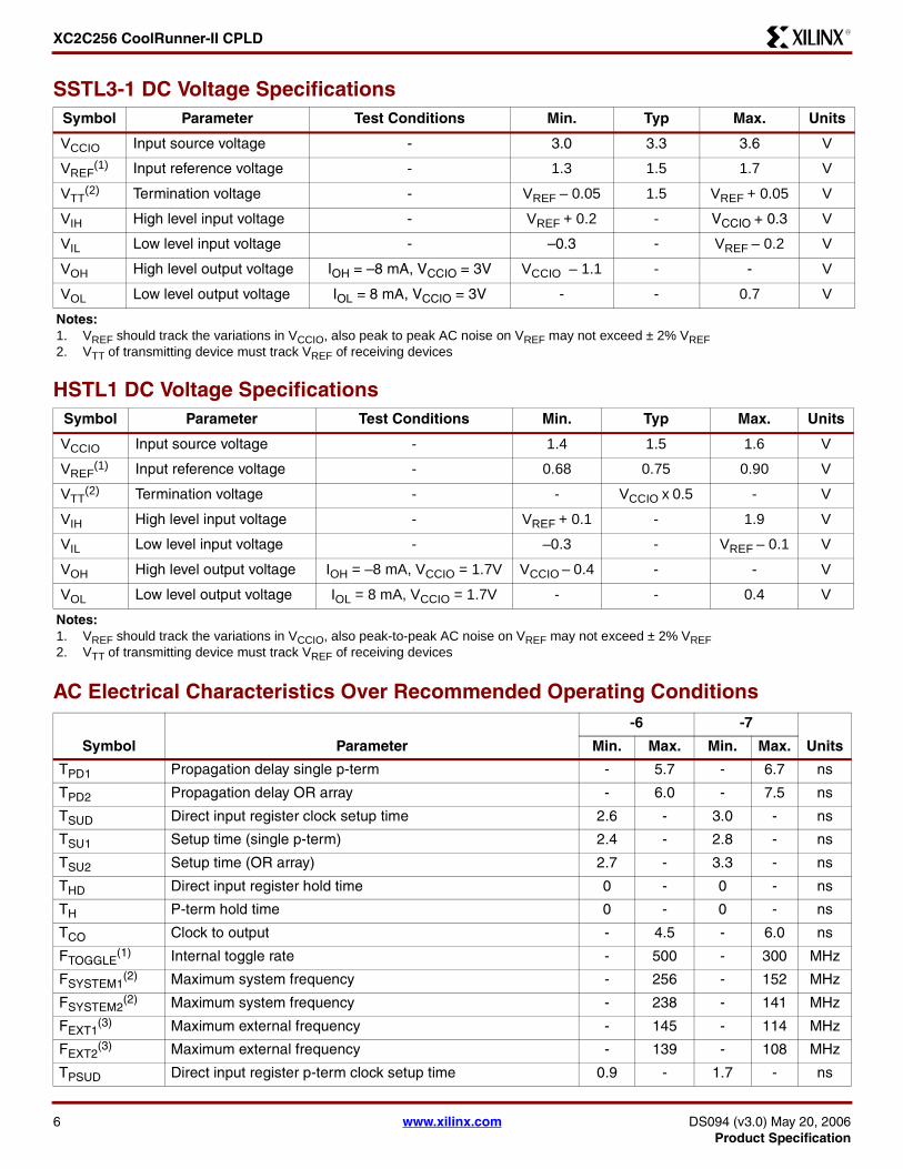
XC2C256 CoolRunner-II CPLDR
SSTL3-1 DC Voltage Specifications
HSTL1 DC Voltage Specifications
AC Electrical Characteristics Over Recommended Operating Conditions
Symbol Parameter Test Conditions Min Typ Max Units
VCCIO Input source voltage - 30 33 36 V
VREF(1) Input reference voltage - 13 15 17 V
VTT(2) Termination voltage - VREF ndash 005 15 VREF + 005 V
VIH High level input voltage - VREF + 02 - VCCIO + 03 V
VIL Low level input voltage - ndash03 - VREF ndash 02 V
VOH High level output voltage IOH = ndash8 mA VCCIO = 3V VCCIO ndash 11 - - V
VOL Low level output voltage IOL = 8 mA VCCIO = 3V - - 07 V
Notes 1 VREF should track the variations in VCCIO also peak to peak AC noise on VREF may not exceed plusmn 2 VREF2 VTT of transmitting device must track VREF of receiving devices
Symbol Parameter Test Conditions Min Typ Max Units
VCCIO Input source voltage - 14 15 16 V
VREF(1) Input reference voltage - 068 075 090 V
VTT(2) Termination voltage - - VCCIO x 05 - V
VIH High level input voltage - VREF + 01 - 19 V
VIL Low level input voltage - ndash03 - VREF ndash 01 V
VOH High level output voltage IOH = ndash8 mA VCCIO = 17V VCCIO ndash 04 - - V
VOL Low level output voltage IOL = 8 mA VCCIO = 17V - - 04 V
Notes 1 VREF should track the variations in VCCIO also peak-to-peak AC noise on VREF may not exceed plusmn 2 VREF2 VTT of transmitting device must track VREF of receiving devices
Symbol Parameter
-6 -7
UnitsMin Max Min Max
TPD1 Propagation delay single p-term - 57 - 67 ns
TPD2 Propagation delay OR array - 60 - 75 ns
TSUD Direct input register clock setup time 26 - 30 - ns
TSU1 Setup time (single p-term) 24 - 28 - ns
TSU2 Setup time (OR array) 27 - 33 - ns
THD Direct input register hold time 0 - 0 - ns
TH P-term hold time 0 - 0 - ns
TCO Clock to output - 45 - 60 ns
FTOGGLE(1) Internal toggle rate - 500 - 300 MHz
FSYSTEM1(2) Maximum system frequency - 256 - 152 MHz
FSYSTEM2(2) Maximum system frequency - 238 - 141 MHz
FEXT1(3) Maximum external frequency - 145 - 114 MHz
FEXT2(3) Maximum external frequency - 139 - 108 MHz
TPSUD Direct input register p-term clock setup time 09 - 17 - ns
6 wwwxilinxcom DS094 (v30) May 20 2006Product Specification
XC2C256 CoolRunner-II CPLDR
TPSU1 P-term clock setup time (single p-term) 07 - 15 - ns
TPSU2 P-term clock setup time (OR array) 10 - 20 - ns
TPHD Direct input register p-term clock hold time 09 - 12 - ns
TPH P-term clock hold 07 - 10 - ns
TPCO P-term clock to output - 62 - 73 ns
TOETOD Global OE to output enabledisable - 56 - 70 ns
TPOETPOD P-term OE to output enabledisable - 70 - 80 ns
TMOETMOD Macrocell driven OE to output enabledisable - 74 - 99 ns
TPAO P-term setreset to output valid - 70 - 81 ns
TAO Global setreset to output valid - 55 - 76 ns
TSUEC Register clock enable setup time 25 - 31 - ns
THEC Register clock enable hold time 0 - 0 - ns
TCW Global clock pulse width High or Low 14 - 22 - ns
TPCW P-term pulse width High or Low 60 - 75 - ns
TAPRPW Asynchronous presetreset pulse width (High or Low) 60 - 75 - ns
TDGSU Set-up before DataGATE latch assertion 0 - 0 - ns
TDGH Hold to DataGATE latch assertion 40 - 60 - ns
TDGR DataGATE recovery to new data - 82 - 90 ns
TDGW DataGATE low pulse width 25 - 35 - ns
TCDRSU CDRST setup time before falling edge GCLK2 13 - 20 - ns
TCDRH Hold time CDRST after falling edge GCLK2 0 - 0 - ns
TCONFIG(4) Configuration time - 150 - 150 μs
Notes 1 FTOGGLE is the maximum clock frequency to which a T-Flip Flop can reliably toggle (see the CoolRunner-II family data sheet for more
information)2 FSYSTEM1 (1TCYCLE) is the internal operating frequency for a device fully populated with one 16-bit counter through one p-term per
macrocell while FSYSTEM2 is through the OR array3 FEXT1 (1TSU1+TCO) is the maximum external frequency using one p-term while FEXT2 is through the OR array4 Typical configuration current during TCONFIG is approximately 77 mA
Symbol Parameter
-6 -7
UnitsMin Max Min Max
DS094 (v30) May 20 2006 wwwxilinxcom 7Product Specification
XC2C256 CoolRunner-II CPLDR
(
Internal Timing Parameters
Symbol Parameter(2)
-6 -7
UnitsMin Max Min Max
Buffer Delays
TIN Input buffer delay - 24 - 26 ns
TDIN Direct data register input delay - 31 - 39 ns
TGCK Global Clock buffer delay - 18 - 27 ns
TGSR Global setreset buffer delay - 20 - 35 ns
TGTS Global 3-state buffer delay - 21 - 30 ns
TOUT Output buffer delay - 23 - 26 ns
TEN Output buffer enabledisable delay - 35 - 40 ns
P-term Delays
TCT Control term delay - 11 - 14 ns
TLOGI1 Single P-term delay adder - 05 - 11 ns
TLOGI2 Multiple P-term delay adder - 03 - 05 ns
Macrocell Delay
TPDI Input to output valid - 05 - 07 ns
TSUI Setup before clock 13 - 18 - ns
THI Hold after clock 0 - 0 - ns
TECSU Enable clock setup time 08 - 18 - ns
TECHO Enable clock hold time 0 - 0 - ns
TCOI Clock to output valid - 04 - 07 ns
TAOI Setreset to output valid - 12 - 15 ns
TCDBL Clock doubler delay - 0 - 0 ns
Feedback Delays
TF Feedback delay - 17 - 30 ns
TOEM Macrocell to global OE delay - 17 - 25 ns
IO Standard Time Adder Delays 15V CMOS
TIN15 Standard input adder - 08 - 10 ns
THYS15 Hysteresis input adder - 30 - 40 ns
TOUT15 Output adder - 08 - 10 ns
TSLEW15 Output slew rate adder - 40 - 50 ns
IO Standard Time Adder Delays 18V CMOS
THYS18 Hysteresis input adder - 20 - 30 ns
TOUT18 Output adder - 0 - 0 ns
TSLEW Output slew rate adder - 20 - 40 ns
8 wwwxilinxcom DS094 (v30) May 20 2006Product Specification
XC2C256 CoolRunner-II CPLDR
Switching Characteristics AC Test Circuit
IO Standard Time Adder Delays 25V CMOS
TIN25 Standard input adder - 06 - 07 ns
THYS25 Hysteresis input adder - 15 - 30 ns
TOUT25 Output adder - 08 - 10 ns
TSLEW25 Output slew rate adder - 30 - 40 ns
IO Standard Time Adder Delays 33V CMOSTTL
TIN33 Standard input adder - 05 - 07 ns
THYS33 Hysteresis input adder - 12 - 30 ns
TOUT33 Output adder - 12 - 16 ns
TSLEW33 Output slew rate adder - 30 - 40 ns
IO Standard Time Adder Delays HSTL SSTL
SSTL2-1 Input adder to TIN TDIN TGCK TGSRTGTS - 04 - 10 ns
Output adder to TOUT - -05 - 00 ns
SSTL3-1 Input adder to TIN TDIN TGCK TGSRTGTS - 04 - 10 ns
Output adder to TOUT - -05 - 00 ns
HSTL-1 Input adder to TIN TDIN TGCK TGSRTGTS - 06 - 10 ns
Output adder to TOUT - 0 - 0 ns
Notes 1 15 ns input pin signal risefall
Internal Timing Parameters (Continued)
Symbol Parameter(2)
-6 -7
UnitsMin Max Min Max
Figure 2 Derating Curve for TPD
Number of Outputs Switching
1 2 4 8 1630
40
50
VCC = VCCIO = 18V T = 25oC
T PD
2 (n
s)
55
45
35
DS092_02_092302
Figure 3 AC Load Circuit
R1
VCC
CLR2
Device Under Test
Output Type
LVTTL33
LVCMOS33
LVCMOS25
LVCMOS18
LVCMOS15
CL includes test fixtures and probe capacitance
15 nsec maximum risefall times on inputs
R1
268Ω 275Ω188Ω
1125Ω150Ω
R2
235Ω275Ω188Ω
1125Ω150Ω
CL
35 pF
35 pF
35pF
35pF
35pF
DS ACT 08 14 02
Test Point
DS094 (v30) May 20 2006 wwwxilinxcom 9Product Specification
XC2C256 CoolRunner-II CPLDR
Figure 4 Typical IV Curve for XC2C256
VO (Output Volts) XC256_VoIo_all_020703
IO (
Out
put C
urre
nt m
A)
00
40
10
50
20
30
60
30252015105 35
33V
15V
18V
25V
Iol
10 wwwxilinxcom DS094 (v30) May 20 2006Product Specification
XC2C256 CoolRunner-II CPLDR
11
Pin DescriptionsFunction
BlockMacro-
cell VQ100 CP132 TQ144 PQ208 FT256IO
Bank
1 1 - - - 2 B3 2
1 2 - - - 208 B4 2
1(GSR) 3 99 A3 143 206 C4 2
1 4 - - 142 205 A2 2
1 5 - - - 203 A3 2
1 6 97 B4 140 202 A4 2
1 7 - - - - - -
1 8 - - - - - -
1 9 - - - - - -
1 10 - - - - - -
1 11 - - - - - -
1 12 96 - 139 201 B5 2
1 13 95 - 138 200 A5 2
1 14 94 A4 137 199 E8 2
1 15 - - - 198 B6 2
1 16 - C5 - 197 C7 2
2(GTS2) 1 1 A1 2 3 D3 2
2 2 - - - 4 C3 2
2(GTS3) 3 2 B2 3 5 E3 2
2 4 - B1 4 6 B2 2
2(GTS0) 5 3 C3 5 7 D4 2
2 6 - - - 8 D2 2
2 7 - - - - - -
2 8 - - - - - -
2 9 - - - - - -
2 10 - - - - - -
2 11 - - - - - -
2(GTS1) 12 4 C2 6 9 E5 2
2 13 - C1 7 10 B1 2
2 14 6 D2 9 12 E4 2
2 15 7 - 10 14 C1 2
2 16 - D1 - - E2 2
3 1 - - 136 196 A6 2
3 2 - B5 135 195 D7 2
3 3 - - 134 194 B7 2
3 4 - A5 - 193 E9 2
3 5 93 - 133 192 A7 2
3 6 C6 191 D8 2
3 7 - - - - - -
3 8 - - - - - -
3 9 - - - - - -
3 10 - - - - - -
3 11 - - - - - -
3 12 92 - - 189 B8 2
3 13 - B6 - 188 C8 2
3 14 91 A6 132 187 A8 2
3 15 - C7 - 186 E11 2
3 16 90 B7 131 185 E10 2
4 1 8 E3 11 15 F2 2
4 2 9 - 12 16 F3 2
4 3 10 E2 13 17 G4 2
4 4 - E1 14 18 G3 2
4 5 11 F3 15 19 F5 2
4 6 12 F2 16 20 G5 2
4 7 - - - - - -
4 8 - - - - - -
4 9 - - - - - -
4 10 - - - - - -
4 11 - - - - - -
4 12 - F1 17 21 H2 2
4 13 13 G1 - 22 H4 2
4 14 - - 18 23 H3 2
4 15 - - - - H1 2
4 16 - - - 25 H5 2
Pin Descriptions (Continued)Function
BlockMacro-
cell VQ100 CP132 TQ144 PQ208 FT256IO
Bank
DS094 (v30) May 20 2006 wwwxilinxcom 11Product Specification
XC2C256 CoolRunner-II CPLDR
5 1 - L3 - 49 R1 1
5 2 - - 33 48 N4 1
5 3 - - - 47 N2 1
5(GCK1) 4 23 L2 32 46 M3 1
5 5 L1 31 45 P1 1
5(GCK0) 6 22 K3 30 44 M2 1
5 7 - - - - - -
5 8 - - - - - -
5 9 - - - - - -
5 10 - - - - - -
5 11 - - - - - -
5 12 - - - 43 L3 1
5 13 - - - 41 N1 1
5 14 - - 28 40 L4 1
5 15 - - - 39 M1 1
5 16 - K1 - 38 L5 1
6 1 - M1 34 50 N3 1
6 (CDRST)
2 24 M2 35 51 P2 1
6 3 - - - 54 P4 1
6(GCK2) 4 27 N2 38 55 P5 1
6 5 - - - 56 R2 1
6 6 - - - 57 T1 1
6 7 - - - - - -
6 8 - - - - - -
6 9 - - - - - -
6 10 - - - - - -
6 11 - - - - - -
6(DGE) 12 28 P2 39 58 T2 1
6 13 - M3 40 60 N5 1
6 14 29 N3 41 61 R4 1
6 15 - P3 42 62 M5 1
6 16 30 M4 43 63 R5 1
Pin Descriptions (Continued)Function
BlockMacro-
cell VQ100 CP132 TQ144 PQ208 FT256IO
Bank
7 1 - - - 37 K4 1
7 2 - - - 36 L2 1
7 3 - - - 35 K3 1
7 4 - - - 34 L1 1
7 5 19 J2 26 32 K5 1
7 6 18 J1 25 31 K2 1
7 7 - - - - - -
7 8 - - - - - -
7 9 - - - - - -
7 10 - - - - - -
7 11 17 H3 24 30 J4 1
7 12 16 H2 23 29 K1 1
7 13 15 H1 22 28 J3 1
7 14 14 G3 21 27 J2 1
7 15 - G2 20 - J5 1
7 16 - - 19 - J1 1
8 1 - N4 44 64 R6 1
8 2 - - 45 65 N6 1
8 3 - - 46 66 R3 1
8 4 - - - 67 M6 1
8 5 - - 48 69 T3 1
8 6 32 - 49 70 P6 1
8 7 - - - - - -
8 8 - - - - - -
8 9 - - - - - -
8 10 - - - - - -
8 11 33 M5 50 71 T4 1
8 12 34 N5 51 72 P7 1
8 13 35 P5 52 73 T5 1
8 14 36 M6 - 74 N7 1
8 15 37 N6 - 75 R7 1
8 16 - - - 76 M7 1
Pin Descriptions (Continued)Function
BlockMacro-
cell VQ100 CP132 TQ144 PQ208 FT256IO
Bank
12 wwwxilinxcom DS094 (v30) May 20 2006Product Specification
XC2C256 CoolRunner-II CPLDR
9 1 78 C12 112 160 B13 2
9 2 79 B12 113 161 B14 2
9 3 - - - 162 C13 2
9 4 80 A12 114 163 A15 2
9 5 164 C12 2
9 6 81 C11 115 165 B12 2
9 7 - - - - - -
9 8 - - - - - -
9 9 - - - - - -
9 10 - - - - - -
9 11 - - - 166 D13 2
9 12 82 B11 116 167 A14 2
9 13 - - 117 168 E13 2
9 14 - A11 118 169 A13 2
9 15 - - 119 170 C11 2
9 16 - C10 - 171 A12 2
10 1 77 A13 111 159 A16 2
10 2 76 B13 110 158 B15 2
10 3 74 C13 107 155 C14 2
10 4 73 C14 106 154 G11 2
10 5 72 D12 105 153 B16 2
10 6 71 D13 104 152 D15 2
10 7 - - - - - -
10 8 - - - - - -
10 9 - - - - - -
10 10 - - - - - -
10 11 151 E14 2
10 12 70 D14 103 150 C16 2
10 13 - - - 149 F14 2
10 14 - E12 102 148 F13 2
10 15 - - - 147 E15 2
10 16 - E13 101 146 G13 2
Pin Descriptions (Continued)Function
BlockMacro-
cell VQ100 CP132 TQ144 PQ208 FT256IO
Bank
11 1 - B10 - - B11 2
11 2 - - 173 D11 2
11 3 - A10 - 174 A11 2
11 4 - - - 175 D10 2
11 5 - C9 120 - B10 2
11 6 - - 121 - E12 2
11 7 - - - - - -
11 8 - - - - - -
11 9 - - - - - -
11 10 - - - - - -
11 11 85 A8 124 178 F12 2
11 12 86 B8 125 179 B9 2
11 13 87 C8 126 180 C9 2
11 14 89 - 128 182 C10 2
11 15 - - 129 183 A9 2
11 16 - - 130 184 D9 2
12 1 - - - 145 F15 2
12 2 - - 100 144 G14 2
12 3 - - - 143 E16 2
12 4 - - - 142 H12 2
12 5 - F12 - 140 F16 2
12 6 - F13 - 139 H16 2
12 7 - - - - - -
12 8 - - - - - -
12 9 - - - - - -
12 10 - - - - - -
12 11 68 F14 98 138 G15 2
12 12 - G12 97 137 H13 2
12 13 67 G13 96 136 G16 2
12 14 66 - 95 135 H14 2
12 15 65 - 94 134 H15 2
12 16 - - - - J12 2
Pin Descriptions (Continued)Function
BlockMacro-
cell VQ100 CP132 TQ144 PQ208 FT256IO
Bank
DS094 (v30) May 20 2006 wwwxilinxcom 13Product Specification
XC2C256 CoolRunner-II CPLDR
13 1 - N13 75 107 R15 1
13 2 53 N14 76 108 T16 1
13 3 - M12 77 109 N14 1
13 4 54 - - 110 R16 1
13 5 - M13 78 111 N15 1
13 6 55 - 79 112 M15 1
13 7 - - - - - -
13 8 - - - - - -
13 9 - - - - - -
13 10 - - - - - -
13 11 - - - - - -
13 12 - M14 80 113 M13 1
13 13 56 - 81 114 P16 1
13 14 - L12 82 115 N16 1
13 15 - - - 116 L14 1
13 16 - L13 - 117 M14 1
14 1 52 P14 74 106 P15 1
14 2 - - 71 103 P14 1
14 3 50 P12 70 102 P13 1
14 4 - M11 69 101 R13 1
14 5 49 N11 - 100 N13 1
14 6 - P11 68 - R14 1
14 7 - - - - - -
14 8 - - - - - -
14 9 - - - - - -
14 10 - - - - - -
14 11 - - - - - -
14 12 - - - 99 T15 1
14 13 - - 66 97 R12 1
14 14 46 P10 64 95 N11 1
14 15 44 - - - M11 1
14 16 - P9 61 91 N10 1
Pin Descriptions (Continued)Function
BlockMacro-
cell VQ100 CP132 TQ144 PQ208 FT256IO
Bank
15 1 - - - 118 L15 1
15 2 - L14 83 119 L13 1
15 3 - - - 120 M12 1
15 4 - - - 121 M16 1
15 5 - - - 122 K14 1
15 6 - - - 123 L16 1
15 7 - - - - - -
15 8 - - - - - -
15 9 - - - - - -
15 10 - - - - - -
15 11 58 K13 85 125 K15 1
15 12 59 K14 86 126 L12 1
15 13 60 J12 87 127 K16 1
15 14 61 J13 88 128 J14 1
15 15 63 H13 91 - J15 1
15 16 64 H12 92 131 J13 1
16 1 - - - 90 P10 1
16 2 - - - 89 R10 1
16 3 - M8 - 88 T10 1
16 4 - - - 87 R9 1
16 5 43 N8 60 86 N9 1
16 6 42 - 59 85 M8 1
16 7 - - - - - -
16 8 - - - - - -
16 9 - - - - - -
16 10 - - - - - -
16 11 41 P8 58 84 T8 1
16 12 40 M7 57 83 P8 1
16 13 39 N7 56 82 R8 1
16 14 - - - 80 T7 1
16 15 - - 54 78 N8 1
16 16 - P6 53 77 T6 1
Notes 1 GTS = global output enable GSR = global resetset GCK =
global clock CDRST = clock divide reset DGE = DataGATE enable
2 GTS GSR and GCK pins can be used for general purpose IO
Pin Descriptions (Continued)Function
BlockMacro-
cell VQ100 CP132 TQ144 PQ208 FT256IO
Bank
14 wwwxilinxcom DS094 (v30) May 20 2006Product Specification
XC2C256 CoolRunner-II CPLDR
XC2C256 JTAG PowerGround No Connect Pins and Total User IO
Pin Type VQ100 CP132 TQ144 PQ208 FT256
TCK 48 M10 67 98 P12
TDI 45 M9 63 94 R11
TDO 83 B9 122 176 A10
TMS 47 N10 65 96 N12
VCCAUX (JTAG supply voltage)
5 D3 8 11 F4
Power internal (VCC) 26 57 P1 K12 A2 1 37 84 1 53 124 P3 K13 D12 D5
Power Bank 1 IO (VCCIO1) 20 38 51 J3 P7 G14 P13
27 55 73 93 33 59 79 92 105 132
J6 K6 L7 L8 J11 K11 L10 L9
Power Bank 2 IO (VCCIO2) 88 98 A14 C4 A7 109 127 141 26 133 157 172 181 204
F7 F8 G6 H6 F10 F9 H11
Ground 21 25 31 62 69 75
84 100
K2 N1 P4 N9 N12 J14 H14 E14 B14
A9 B3
29 36 47 62 72 89 90 99 108 123 144
13 24 42 52 68 81 93 104 129 130 141 156 177 190
207
F11 F6 G10 G7 G8 G9 H10 H7 H8 H9 J10 J7 J8 J9 K10 K7 K8 K9 L11 L6
No connects - - - - A1 C2 E6 D1 E1 G2 F1 G1 M4 T9 P9 M9 M10 T11 T12 T13 P11 T14 J16 K12 D16 G12 C15 D14 D6 C6 E7 C5
Total user IO 80 106 118 173 184
DS094 (v30) May 20 2006 wwwxilinxcom 15Product Specification
XC2C256 CoolRunner-II CPLDR
Ordering Information
Part NumberPinBall Spacing
θJA (CWatt)
θJC (CWatt) Package Type
Package Body Dimensions IO
Commercial (C)
Industrial (I)(1)
XC2C256-6VQ100C 05mm 431 109 Very Thin Quad Flat Pack
14mm x 14mm 80 C
XC2C256-7VQ100C 05mm 431 109 Very Thin Quad Flat Pack
14mm x 14mm 80 C
XC2C256-6CP132C 05mm 650 150 Chip Scale Package 8mm x 8mm 106 C
XC2C256-7CP132C 05mm 650 150 Chip Scale Package 8mm x 8mm 106 C
XC2C256-6TQ144C 05mm 372 72 Thin Quad Flat Pack 20mm x 20mm 118 C
XC2C256-7TQ144C 05mm 372 72 Thin Quad Flat Pack 20mm x 20mm 118 C
XC2C256-6PQ208C 05mm 369 97 Plastic Quad Flat Pack
28mm x 28mm 173 C
XC2C256-7PQ208C 05mm 369 97 Plastic Quad Flat Pack
28mm x 28mm 173 C
XC2C256-6FT256C 10mm 346 61 Fine Pitch Thin BGA 17mm x 17mm 184 C
XC2C256-7FT256C 10mm 346 61 Fine Pitch Thin BGA 17mm x 17mm 184 C
XC2C256-6VQG100C 05mm 431 109 Very Thin Quad Flat Pack Pb-free
14mm x 14mm 80 C
XC2C256-7VQG100C 05mm 431 109 Very Thin Quad Flat Pack Pb-free
14mm x 14mm 80 C
XC2C256-6CPG132C 05mm 650 150 Chip Scale Package Pb-free
8mm x 8mm 106 C
XC2C256-7CPG132C 05mm 650 150 Chip Scale Package Pb-free
8mm x 8mm 106 C
XC2C256-6TQG144C 05mm 372 72 Thin Quad Flat Pack Pb-free
20mm x 20mm 118 C
XC2C256-7TQG144C 05mm 372 72 Thin Quad Flat Pack Pb-free
20mm x 20mm 118 C
XC2C256-6PQG208C 05mm 369 97 Plastic Quad Flat Pack Pb-free
28mm x 28mm 173 C
XC2C256-7PQG208C 05mm 369 97 Plastic Quad Flat Pack Pb-free
28mm x 28mm 173 C
XC2C256-6FTG256C 10mm 346 61 Fine Pitch Thin BGA Pb-free
17mm x 17mm 184 C
XC2C256-7FTG256C 10mm 346 61 Fine Pitch Thin BGA Pb-free
17mm x 17mm 184 C
XC2C256-7VQ100I 05mm 431 109 Very Thin Quad Flat Pack
14mm x 14mm 80 I
XC2C256-7CP132I 05mm 650 150 Chip Scale Package 8mm x 8mm 106 I
XC2C256-7TQ144I 05mm 372 72 Thin Quad Flat Pack 20mm x 20mm 118 I
XC2C256-7PQ208I 05mm 369 97 Plastic Quad Flat Pack
28mm x 28mm 173 I
XC2C256-7FT256I 10mm 346 61 Fine Pitch Thin BGA 17mm x 17mm 184 I
16 wwwxilinxcom DS094 (v30) May 20 2006Product Specification
XC2C256 CoolRunner-II CPLDR
Device Part Marking
Figure 5 Sample Package with Part Marking
Note Due to the small size of chip scale packages the complete ordering part number cannot be included on the packagemarking Part marking on chip scale packages by line are
bull Line 1 = X (Xilinx logo) then truncated part numberbull Line 2 = Not related to device part numberbull Line 3 = Not related to device part number
1 Line 4 = Package code speed operating temperature three digits not related to device part number Package codes C5 = CP132 C6 = CPG132
XC2C256-7VQG100I 05mm 431 109 Very Thin Quad Flat Pack Pb-free
14mm x 14mm 80 I
XC2C256-7CPG132I 05mm 650 150 Chip Scale Package Pb-free
8mm x 8mm 106 I
XC2C256-7TQG144I 05mm 372 72 Thin Quad Flat Pack Pb-free
20mm x 20mm 118 I
XC2C256-7PQG208I 05mm 369 97 Plastic Quad Flat Pack Pb-free
28mm x 28mm 173 I
XC2C256-7FTG256I 10mm 346 61 Fine Pitch Thin BGA Pb-free
17mm x 17mm 184 I
Notes 1 C = Commercial (TA = 0degC to +70degC) I = Industrial (TA = ndash40degC to +85degC)
Part NumberPinBall Spacing
θJA (CWatt)
θJC (CWatt) Package Type
Package Body Dimensions IO
Commercial (C)
Industrial (I)(1)
Standard Example XC2C128 Device Speed Grade Package Type Number of Pins Temperature Range
-6 TQ C144 Pb-Free Example XC2C128 TQ G 144 C
Device Speed Grade Package Type Pb-FreeNumber of Pins
-6
Temperature Range
XC2Cxxx
TQ144
7C
Device Type
Package
Speed
Operating Range
This line not
related to device
part number
R
Part marking for non-chip scale package
DS094 (v30) May 20 2006 wwwxilinxcom 17Product Specification
XC2C256 CoolRunner-II CPLDR
Figure 6 VQ100 Very Thin Quad Flat Pack
VQ100Top View
GN
DIO
(3)
VC
CIO
2IO IO IO IO IO IO IO IO IO V
CC
IO2
IO IO IO GN
DT
DO
IO IO IO IO IO IO IO
VC
CIO
(2)
IO(5
)
IO IOG
ND
IO IO IO IO IO IOV
CC
IO1
IO IO IO IO IO IO TD
IIO
TM
ST
CK
IO IO
GNDIOIOIOIOIOGNDIOIOIOIOIOIOGNDIOIOIOIOVCCIOIOIOIOIOVCCIO1
IO(1)IO(1)IO(1)IO(1)VAUX
IOIOIOIOIOIOIOIOIOIOIOIOIOIO
VCCIO1GND
IO(2)IO(2)IO(4)GND
12345678910111213141516171819202122232425
75747372717069686766656463626160595857565554535251
26 27 28 29 30 31 32 33 34 35 36 37 38 39 40 41 42 43 44 45 46 47 48 49 50
100 99 98 97 96 95 94 93 92 91 90 89 88 87 86 85 84 83 82 81 80 79 78 77 76
(1) - Global Output Enable(2) - Global Clock(3) - Global SetReset(4) - Clock Divide Reset(5) - Data Gate
18 wwwxilinxcom DS094 (v30) May 20 2006Product Specification
XC2C256 CoolRunner-II CPLDR
Figure 7 CP132 Chip Scale Package
CP132Bottom View
P
N
M
L
K
J
H
G
F
E
D
C
B
A
1 2 3 4 5 6 7 8 9 10 11 12 13 14
VCC VCCIO1 VCCIO1GNDIO IO IO IO IO IO IO IO IOIO(5)
IO IOVAUX IO IOIO
IO IOIO IO IOIO
IO IOIO IO VCCIO1IO
IO IOIO IO GNDIO
IO IOIO IO GNDIO
IO IOVCCIO1 IO GNDIO
IO IOIO(2) VCC IOGND
IO IOIO IO IOIO(2)
IO(1) VCCIO2 IOIOIO(3) IO IO IO GND IO IO IO VCCIO2VCC
IO IO IOIOGND IO IO IO TDO IO IO IO GNDIO(1)
IO IO IOVCCIO2IO(1) IO IO IO IO IO IO IO IOIO(1)
IO IO IOIOIO IO IO IO TDI TCK IO IO IOIO(4)
GND IO IOIOIO IO IO IO GND TMS IO GND IOIO(2)
(1) - Global Output Enable(2) - Global Clock(3) - Global SetReset(4) - Clock Divide Reset(5) - DataGATE Enable
DS094 (v30) May 20 2006 wwwxilinxcom 19Product Specification
XC2C256 CoolRunner-II CPLDR
Figure 8 TQ144 Thin Quad Flat Pack
VCCIO(1)
IO(1)
IOIO(1)
IO(1)
IOVAUX
IOIOIOIOIOIOIOIOIOIOIOIOIOIOIOIOIOIO
VCCIO1IO
GNDIO(2)
IOIO(2)
IOIO
IO(4)
GND
123456789101112131415161718192021222324252627282930313233343536
TQ144Top View
VC
CIO
(2)
IO(5
)
IO IO IO IO IO IO IOG
ND
IO IO IO IO IO IO IOV
CC
IO1
IO IO IO IO IO IOG
ND
TD
IIO
TM
SIO
TC
KIO IO IO IO
GN
D
108107106105104103102101100999897969594939291908988878685848382818079787776757473
37 38 39 40 41 42 43 44 45 46 47 48 49 50 51 52 53 54 55 56 57 58 59 60 61 62 63 64 65 66 67 68 69 70 71 72
144
143
142
141
140
139
138
137
136
135
134
133
132
131
130
129
128
127
126
125
124
123
122
121
120
119
118
117
116
115
114
113
112
111
110
109
GNDIOIOIOIOIOIOIOIOGNDIOIOIOIOIOVCCIO1IOIOGNDGNDIOIOIOIOVCCIOIOIOIOIOIOIOIOIOIOVCCIO1
GN
DIO
(3)
IO VC
CIO
2IO IO IO IO IO IO IO IO IO IO IO IO IO V
CC
IO2
IO IO IO GN
DT
DO
IO IO IO IO IO IO IO IO IO IO IO IO VC
CIO
2
(1) - Global Output Enable(2) - Global Clock(3) - Global SetReset(4) - Clock Divide Reset(5) - DataGATE Enable
20 wwwxilinxcom DS094 (v30) May 20 2006Product Specification
XC2C256 CoolRunner-II CPLDR
Figure 9 PQ208 Quad Flat Package
VCCIO
IO(1)IO
IO(1)IO
IO(1)IO
IO(1)IO
VAUXIO
GNDIOIOIOIOIOIOIOIOIOIO
GNDIO
VCCIO2IOIOIOIOIOIO
VCCIO1IOIOIOIOIOIOIOIO
GNDIO
IO(2)IO
IO(2)IOIOIOIO
IO(4)GND
PQ208Top View
VC
CI
OI
O(2
)I
OI
OI
O(5
)V
CC
IO1
IO
IO
IO
IO
IO
IO
IO
IO
GN
DI
OI
OI
OI
OI
OI
OI
OI
OI
OI
OV
CC
IO1
IO
GN
DI
OI
OI
OI
OI
OI
OI
OI
OI
OI
OV
CC
IO1
GN
DT
DI
IO
TM
SI
OT
CK
IO
IO
IO
IO
IO
GN
D
(1) - Global Output Enable(2) - Global Clock(3) - Global SetReset(4) - Clock Divide Reset(5) - DataGATE Enable
GNDIOIOIOIOIOIOIOIOIOIOIOIOIOIOGNDIOIOIOIOIOIOIOVCCIO2VCCIO1IOGNDGNDIOIOIOIOVCCIOIOIOIOIOIOIOIOIOIOIOIOIOIOIOIOIOIOVCCIO1
IO GN
DIO
(3)
IO VC
CIO
2IO IO IO IO IO IO IO IO IO IO IO IO IO G
ND
IO IO IO IO IO IO IO IO VC
CIO
2IO IO IO G
ND
TD
OIO IO IO V
CC
IO2
IO IO IO IO IO IO IO IO IO IO IO IO IO IO VC
CIO
2
12345678910111213141516171819202122232425262728293031323334353637383940414243444546474849505152
53 54 55 56 57 58 59 60 61 62 63 64 65 66 67 68 69 70 71 72 73 74 75 76 77 78 79 80 81 82 83 84 85 86 87 88 89 90 91 92 93 94 95 96 97 98 99 100
101
102
103
104
156155154153152151150149148147146145144143142141140139138137136135134133132131130129128127126125124123122121120119118117116115114113112111110109108107106105
208
207
206
205
204
203
202
201
200
199
198
197
196
195
194
193
192
191
190
189
188
187
186
185
184
183
182
181
180
179
178
177
176
175
174
173
172
171
170
169
168
167
166
165
164
163
162
161
160
159
158
157
DS094 (v30) May 20 2006 wwwxilinxcom 21Product Specification
XC2C256 CoolRunner-II CPLDR
Warranty DisclaimerTHESE PRODUCTS ARE SUBJECT TO THE TERMS OF THE XILINX LIMITED WARRANTY WHICH CAN BE VIEWEDAT httpwwwxilinxcomwarrantyhtm THIS LIMITED WARRANTY DOES NOT EXTEND TO ANY USE OF THEPRODUCTS IN AN APPLICATION OR ENVIRONMENT THAT IS NOT WITHIN THE SPECIFICATIONS STATED ON THETHEN-CURRENT XILINX DATA SHEET FOR THE PRODUCTS PRODUCTS ARE NOT DESIGNED TO BE FAIL-SAFEAND ARE NOT WARRANTED FOR USE IN APPLICATIONS THAT POSE A RISK OF PHYSICAL HARM OR LOSS OFLIFE USE OF PRODUCTS IN SUCH APPLICATIONS IS FULLY AT THE RISK OF CUSTOMER SUBJECT TOAPPLICABLE LAWS AND REGULATIONS
Figure 10 FT256 Fine Pitch Thin BGA
FT256 Bottom View
A
B
C
D
E
F
G
H
J
K
L
M
N
P
R
T
16 15 14 13 12 11 10 9 8 7 6 5 4 3 2 1
IO TDO IOIOIO IO IO IO IO IO IO IO IO IO NCIO
IO IO IOIOIO IO IO IO IO IO IO IO IO IO IOIO
IO IO IO(3)IOIO IO IO IO IO IO NC NC IO NC IONC
NC IO IO(1)IONC VCC IO IO IO IO NC VCC IO(1) IO NCIO
IO IO IOIOIO IO IO IO IO NC NC IO(1) IO(1) IO NCIO
IO VCCIO2 VAUXIOIO IO GND VCCIO2 VCCIO2 VCCIO2 GND IO IO IO NCIO
IO GND IOIOIO NC IO GND GND GND VCCIO2 IO IO NC NCIO
IO GND IOIOIO IO VCCIO2 GND GND GND VCCIO2 IO IO IO IOIO
NC GND IOIOIO IO VCCIO1 GND GND GND VCCIO1 IO IO IO IOIO
IO GND IOVCCIO NC VCCIO1 GND GND GND VCCIO1 IO IO IO IOIO
IO VCCIO1 IOIOIO IO GND VCCIO1 VCCIO1 VCCIO1 GND IO IO IO IOIO
IO NC NCIOIO IO IO NC IO IO IO IO IO(2) IO(2) IOIO
IO IO IOIOIO TMS IO IO IO IO IO IO IO IO IOIO
IO IO IOIOIO TCK NC NC IO IO IO IO(2) VCC IO(4) IOIO
IO IO IOIOIO IO TDI IO IO IO IO IO IO IO IOIO
IO IO IONCNC NC NC NC IO IO IO IO IO IO(5) IOIO
(1) - Global Output Enable(2) - Global Clock(3) - Global SetReset(4) - Clock Divide Reset(5) - DataGATE Enable
22 wwwxilinxcom DS094 (v30) May 20 2006Product Specification
XC2C256 CoolRunner-II CPLDR
Additional InformationAdditional information is available for the following CoolRunner-II topics
bull XAPP784 Bulletproof CPLD Design Practicesbull XAPP375 Timing Model bull XAPP376 Logic Engine bull XAPP378 Advanced Features bull XAPP382 IO Characteristics bull XAPP389 Powering CoolRunner-II bull XAPP399 Assigning VREF Pins
To access these and all application notes with their associ-ated reference designs click the following link and scrolldown the page until you find the document you want
CoolRunner-II Data Sheets and Application Notes
Device Packages
Revision HistoryThe following table shows the revision history for this document
Date Version Revision
050902 10 Initial Xilinx release
051302 11 Updated AC Electrical Characteristics and added new parameters
103102 12 Corrected package user IO added Voltage Referenced DC tables
031703 20 Added Characterization numbers for product release and device part marking
040203 21 Updated TSOL max from 260 to 220 Changed ICCSB units from mA to μA
012604 22 Updated Device Part Marking Updated links and Tsol
022604 23 Corrected Theta JC value on XC2C256-7TQ144
080304 24 Pb-free documentation
081904 25 Changes to ICCSB maximum specifications in DC Electrical Characteristics table on page 3
100104 26 Add Asynchronous PresetReset Pulse Width specification to AC Electrical Characteristics
030705 27 Removed -5 speed grade Changes to Table 1 IO Standards
062805 28 Move to Product Specification Change to TIN25 TOUT25 TIN33 and TOUT33 for -7 speed grade
032006 29 Add Warranty Disclaimer Add note to Pin Description table that GTS GSR and GCK pins can be used for general purpose IO
52006 30 Moved TCONFIG specification values from MIN column to MAX column page 7
DS094 (v30) May 20 2006 wwwxilinxcom 23Product Specification
- Features
- Description
- RealDigital Design Technology
- Supported IO Standards
- Absolute Maximum Ratings
- Recommended Operating Conditions
- DC Electrical Characteristics (Over Recommended Operating Conditions)
- LVCMOS 33V and LVTTL 33V DC Voltage Specifications
- LVCMOS 25V DC Voltage Specifications
- LVCMOS 18V DC Voltage Specifications
- LVCMOS 15V DC Voltage Specifications(1)
- Schmitt Trigger Input DC Voltage Specifications
- SSTL2-1 DC Voltage Specifications
- SSTL3-1 DC Voltage Specifications
- HSTL1 DC Voltage Specifications
- AC Electrical Characteristics Over Recommended Operating Conditions
- Internal Timing Parameters
-
- Switching Characteristics
- AC Test Circuit
-
- Pin Descriptions
-
- XC2C256 JTAG PowerGround No Connect Pins and Total User IO
-
- Warranty Disclaimer
- Additional Information
- Revision History
-
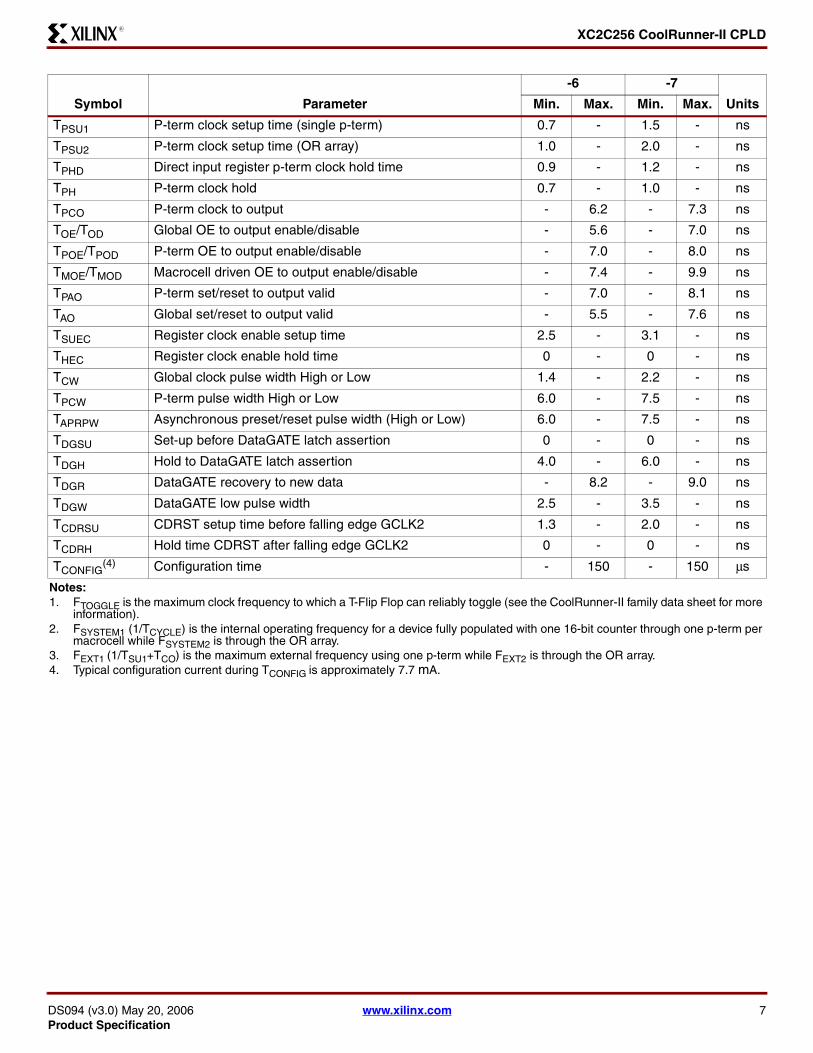
XC2C256 CoolRunner-II CPLDR
TPSU1 P-term clock setup time (single p-term) 07 - 15 - ns
TPSU2 P-term clock setup time (OR array) 10 - 20 - ns
TPHD Direct input register p-term clock hold time 09 - 12 - ns
TPH P-term clock hold 07 - 10 - ns
TPCO P-term clock to output - 62 - 73 ns
TOETOD Global OE to output enabledisable - 56 - 70 ns
TPOETPOD P-term OE to output enabledisable - 70 - 80 ns
TMOETMOD Macrocell driven OE to output enabledisable - 74 - 99 ns
TPAO P-term setreset to output valid - 70 - 81 ns
TAO Global setreset to output valid - 55 - 76 ns
TSUEC Register clock enable setup time 25 - 31 - ns
THEC Register clock enable hold time 0 - 0 - ns
TCW Global clock pulse width High or Low 14 - 22 - ns
TPCW P-term pulse width High or Low 60 - 75 - ns
TAPRPW Asynchronous presetreset pulse width (High or Low) 60 - 75 - ns
TDGSU Set-up before DataGATE latch assertion 0 - 0 - ns
TDGH Hold to DataGATE latch assertion 40 - 60 - ns
TDGR DataGATE recovery to new data - 82 - 90 ns
TDGW DataGATE low pulse width 25 - 35 - ns
TCDRSU CDRST setup time before falling edge GCLK2 13 - 20 - ns
TCDRH Hold time CDRST after falling edge GCLK2 0 - 0 - ns
TCONFIG(4) Configuration time - 150 - 150 μs
Notes 1 FTOGGLE is the maximum clock frequency to which a T-Flip Flop can reliably toggle (see the CoolRunner-II family data sheet for more
information)2 FSYSTEM1 (1TCYCLE) is the internal operating frequency for a device fully populated with one 16-bit counter through one p-term per
macrocell while FSYSTEM2 is through the OR array3 FEXT1 (1TSU1+TCO) is the maximum external frequency using one p-term while FEXT2 is through the OR array4 Typical configuration current during TCONFIG is approximately 77 mA
Symbol Parameter
-6 -7
UnitsMin Max Min Max
DS094 (v30) May 20 2006 wwwxilinxcom 7Product Specification
XC2C256 CoolRunner-II CPLDR
(
Internal Timing Parameters
Symbol Parameter(2)
-6 -7
UnitsMin Max Min Max
Buffer Delays
TIN Input buffer delay - 24 - 26 ns
TDIN Direct data register input delay - 31 - 39 ns
TGCK Global Clock buffer delay - 18 - 27 ns
TGSR Global setreset buffer delay - 20 - 35 ns
TGTS Global 3-state buffer delay - 21 - 30 ns
TOUT Output buffer delay - 23 - 26 ns
TEN Output buffer enabledisable delay - 35 - 40 ns
P-term Delays
TCT Control term delay - 11 - 14 ns
TLOGI1 Single P-term delay adder - 05 - 11 ns
TLOGI2 Multiple P-term delay adder - 03 - 05 ns
Macrocell Delay
TPDI Input to output valid - 05 - 07 ns
TSUI Setup before clock 13 - 18 - ns
THI Hold after clock 0 - 0 - ns
TECSU Enable clock setup time 08 - 18 - ns
TECHO Enable clock hold time 0 - 0 - ns
TCOI Clock to output valid - 04 - 07 ns
TAOI Setreset to output valid - 12 - 15 ns
TCDBL Clock doubler delay - 0 - 0 ns
Feedback Delays
TF Feedback delay - 17 - 30 ns
TOEM Macrocell to global OE delay - 17 - 25 ns
IO Standard Time Adder Delays 15V CMOS
TIN15 Standard input adder - 08 - 10 ns
THYS15 Hysteresis input adder - 30 - 40 ns
TOUT15 Output adder - 08 - 10 ns
TSLEW15 Output slew rate adder - 40 - 50 ns
IO Standard Time Adder Delays 18V CMOS
THYS18 Hysteresis input adder - 20 - 30 ns
TOUT18 Output adder - 0 - 0 ns
TSLEW Output slew rate adder - 20 - 40 ns
8 wwwxilinxcom DS094 (v30) May 20 2006Product Specification
XC2C256 CoolRunner-II CPLDR
Switching Characteristics AC Test Circuit
IO Standard Time Adder Delays 25V CMOS
TIN25 Standard input adder - 06 - 07 ns
THYS25 Hysteresis input adder - 15 - 30 ns
TOUT25 Output adder - 08 - 10 ns
TSLEW25 Output slew rate adder - 30 - 40 ns
IO Standard Time Adder Delays 33V CMOSTTL
TIN33 Standard input adder - 05 - 07 ns
THYS33 Hysteresis input adder - 12 - 30 ns
TOUT33 Output adder - 12 - 16 ns
TSLEW33 Output slew rate adder - 30 - 40 ns
IO Standard Time Adder Delays HSTL SSTL
SSTL2-1 Input adder to TIN TDIN TGCK TGSRTGTS - 04 - 10 ns
Output adder to TOUT - -05 - 00 ns
SSTL3-1 Input adder to TIN TDIN TGCK TGSRTGTS - 04 - 10 ns
Output adder to TOUT - -05 - 00 ns
HSTL-1 Input adder to TIN TDIN TGCK TGSRTGTS - 06 - 10 ns
Output adder to TOUT - 0 - 0 ns
Notes 1 15 ns input pin signal risefall
Internal Timing Parameters (Continued)
Symbol Parameter(2)
-6 -7
UnitsMin Max Min Max
Figure 2 Derating Curve for TPD
Number of Outputs Switching
1 2 4 8 1630
40
50
VCC = VCCIO = 18V T = 25oC
T PD
2 (n
s)
55
45
35
DS092_02_092302
Figure 3 AC Load Circuit
R1
VCC
CLR2
Device Under Test
Output Type
LVTTL33
LVCMOS33
LVCMOS25
LVCMOS18
LVCMOS15
CL includes test fixtures and probe capacitance
15 nsec maximum risefall times on inputs
R1
268Ω 275Ω188Ω
1125Ω150Ω
R2
235Ω275Ω188Ω
1125Ω150Ω
CL
35 pF
35 pF
35pF
35pF
35pF
DS ACT 08 14 02
Test Point
DS094 (v30) May 20 2006 wwwxilinxcom 9Product Specification
XC2C256 CoolRunner-II CPLDR
Figure 4 Typical IV Curve for XC2C256
VO (Output Volts) XC256_VoIo_all_020703
IO (
Out
put C
urre
nt m
A)
00
40
10
50
20
30
60
30252015105 35
33V
15V
18V
25V
Iol
10 wwwxilinxcom DS094 (v30) May 20 2006Product Specification
XC2C256 CoolRunner-II CPLDR
11
Pin DescriptionsFunction
BlockMacro-
cell VQ100 CP132 TQ144 PQ208 FT256IO
Bank
1 1 - - - 2 B3 2
1 2 - - - 208 B4 2
1(GSR) 3 99 A3 143 206 C4 2
1 4 - - 142 205 A2 2
1 5 - - - 203 A3 2
1 6 97 B4 140 202 A4 2
1 7 - - - - - -
1 8 - - - - - -
1 9 - - - - - -
1 10 - - - - - -
1 11 - - - - - -
1 12 96 - 139 201 B5 2
1 13 95 - 138 200 A5 2
1 14 94 A4 137 199 E8 2
1 15 - - - 198 B6 2
1 16 - C5 - 197 C7 2
2(GTS2) 1 1 A1 2 3 D3 2
2 2 - - - 4 C3 2
2(GTS3) 3 2 B2 3 5 E3 2
2 4 - B1 4 6 B2 2
2(GTS0) 5 3 C3 5 7 D4 2
2 6 - - - 8 D2 2
2 7 - - - - - -
2 8 - - - - - -
2 9 - - - - - -
2 10 - - - - - -
2 11 - - - - - -
2(GTS1) 12 4 C2 6 9 E5 2
2 13 - C1 7 10 B1 2
2 14 6 D2 9 12 E4 2
2 15 7 - 10 14 C1 2
2 16 - D1 - - E2 2
3 1 - - 136 196 A6 2
3 2 - B5 135 195 D7 2
3 3 - - 134 194 B7 2
3 4 - A5 - 193 E9 2
3 5 93 - 133 192 A7 2
3 6 C6 191 D8 2
3 7 - - - - - -
3 8 - - - - - -
3 9 - - - - - -
3 10 - - - - - -
3 11 - - - - - -
3 12 92 - - 189 B8 2
3 13 - B6 - 188 C8 2
3 14 91 A6 132 187 A8 2
3 15 - C7 - 186 E11 2
3 16 90 B7 131 185 E10 2
4 1 8 E3 11 15 F2 2
4 2 9 - 12 16 F3 2
4 3 10 E2 13 17 G4 2
4 4 - E1 14 18 G3 2
4 5 11 F3 15 19 F5 2
4 6 12 F2 16 20 G5 2
4 7 - - - - - -
4 8 - - - - - -
4 9 - - - - - -
4 10 - - - - - -
4 11 - - - - - -
4 12 - F1 17 21 H2 2
4 13 13 G1 - 22 H4 2
4 14 - - 18 23 H3 2
4 15 - - - - H1 2
4 16 - - - 25 H5 2
Pin Descriptions (Continued)Function
BlockMacro-
cell VQ100 CP132 TQ144 PQ208 FT256IO
Bank
DS094 (v30) May 20 2006 wwwxilinxcom 11Product Specification
XC2C256 CoolRunner-II CPLDR
5 1 - L3 - 49 R1 1
5 2 - - 33 48 N4 1
5 3 - - - 47 N2 1
5(GCK1) 4 23 L2 32 46 M3 1
5 5 L1 31 45 P1 1
5(GCK0) 6 22 K3 30 44 M2 1
5 7 - - - - - -
5 8 - - - - - -
5 9 - - - - - -
5 10 - - - - - -
5 11 - - - - - -
5 12 - - - 43 L3 1
5 13 - - - 41 N1 1
5 14 - - 28 40 L4 1
5 15 - - - 39 M1 1
5 16 - K1 - 38 L5 1
6 1 - M1 34 50 N3 1
6 (CDRST)
2 24 M2 35 51 P2 1
6 3 - - - 54 P4 1
6(GCK2) 4 27 N2 38 55 P5 1
6 5 - - - 56 R2 1
6 6 - - - 57 T1 1
6 7 - - - - - -
6 8 - - - - - -
6 9 - - - - - -
6 10 - - - - - -
6 11 - - - - - -
6(DGE) 12 28 P2 39 58 T2 1
6 13 - M3 40 60 N5 1
6 14 29 N3 41 61 R4 1
6 15 - P3 42 62 M5 1
6 16 30 M4 43 63 R5 1
Pin Descriptions (Continued)Function
BlockMacro-
cell VQ100 CP132 TQ144 PQ208 FT256IO
Bank
7 1 - - - 37 K4 1
7 2 - - - 36 L2 1
7 3 - - - 35 K3 1
7 4 - - - 34 L1 1
7 5 19 J2 26 32 K5 1
7 6 18 J1 25 31 K2 1
7 7 - - - - - -
7 8 - - - - - -
7 9 - - - - - -
7 10 - - - - - -
7 11 17 H3 24 30 J4 1
7 12 16 H2 23 29 K1 1
7 13 15 H1 22 28 J3 1
7 14 14 G3 21 27 J2 1
7 15 - G2 20 - J5 1
7 16 - - 19 - J1 1
8 1 - N4 44 64 R6 1
8 2 - - 45 65 N6 1
8 3 - - 46 66 R3 1
8 4 - - - 67 M6 1
8 5 - - 48 69 T3 1
8 6 32 - 49 70 P6 1
8 7 - - - - - -
8 8 - - - - - -
8 9 - - - - - -
8 10 - - - - - -
8 11 33 M5 50 71 T4 1
8 12 34 N5 51 72 P7 1
8 13 35 P5 52 73 T5 1
8 14 36 M6 - 74 N7 1
8 15 37 N6 - 75 R7 1
8 16 - - - 76 M7 1
Pin Descriptions (Continued)Function
BlockMacro-
cell VQ100 CP132 TQ144 PQ208 FT256IO
Bank
12 wwwxilinxcom DS094 (v30) May 20 2006Product Specification
XC2C256 CoolRunner-II CPLDR
9 1 78 C12 112 160 B13 2
9 2 79 B12 113 161 B14 2
9 3 - - - 162 C13 2
9 4 80 A12 114 163 A15 2
9 5 164 C12 2
9 6 81 C11 115 165 B12 2
9 7 - - - - - -
9 8 - - - - - -
9 9 - - - - - -
9 10 - - - - - -
9 11 - - - 166 D13 2
9 12 82 B11 116 167 A14 2
9 13 - - 117 168 E13 2
9 14 - A11 118 169 A13 2
9 15 - - 119 170 C11 2
9 16 - C10 - 171 A12 2
10 1 77 A13 111 159 A16 2
10 2 76 B13 110 158 B15 2
10 3 74 C13 107 155 C14 2
10 4 73 C14 106 154 G11 2
10 5 72 D12 105 153 B16 2
10 6 71 D13 104 152 D15 2
10 7 - - - - - -
10 8 - - - - - -
10 9 - - - - - -
10 10 - - - - - -
10 11 151 E14 2
10 12 70 D14 103 150 C16 2
10 13 - - - 149 F14 2
10 14 - E12 102 148 F13 2
10 15 - - - 147 E15 2
10 16 - E13 101 146 G13 2
Pin Descriptions (Continued)Function
BlockMacro-
cell VQ100 CP132 TQ144 PQ208 FT256IO
Bank
11 1 - B10 - - B11 2
11 2 - - 173 D11 2
11 3 - A10 - 174 A11 2
11 4 - - - 175 D10 2
11 5 - C9 120 - B10 2
11 6 - - 121 - E12 2
11 7 - - - - - -
11 8 - - - - - -
11 9 - - - - - -
11 10 - - - - - -
11 11 85 A8 124 178 F12 2
11 12 86 B8 125 179 B9 2
11 13 87 C8 126 180 C9 2
11 14 89 - 128 182 C10 2
11 15 - - 129 183 A9 2
11 16 - - 130 184 D9 2
12 1 - - - 145 F15 2
12 2 - - 100 144 G14 2
12 3 - - - 143 E16 2
12 4 - - - 142 H12 2
12 5 - F12 - 140 F16 2
12 6 - F13 - 139 H16 2
12 7 - - - - - -
12 8 - - - - - -
12 9 - - - - - -
12 10 - - - - - -
12 11 68 F14 98 138 G15 2
12 12 - G12 97 137 H13 2
12 13 67 G13 96 136 G16 2
12 14 66 - 95 135 H14 2
12 15 65 - 94 134 H15 2
12 16 - - - - J12 2
Pin Descriptions (Continued)Function
BlockMacro-
cell VQ100 CP132 TQ144 PQ208 FT256IO
Bank
DS094 (v30) May 20 2006 wwwxilinxcom 13Product Specification
XC2C256 CoolRunner-II CPLDR
13 1 - N13 75 107 R15 1
13 2 53 N14 76 108 T16 1
13 3 - M12 77 109 N14 1
13 4 54 - - 110 R16 1
13 5 - M13 78 111 N15 1
13 6 55 - 79 112 M15 1
13 7 - - - - - -
13 8 - - - - - -
13 9 - - - - - -
13 10 - - - - - -
13 11 - - - - - -
13 12 - M14 80 113 M13 1
13 13 56 - 81 114 P16 1
13 14 - L12 82 115 N16 1
13 15 - - - 116 L14 1
13 16 - L13 - 117 M14 1
14 1 52 P14 74 106 P15 1
14 2 - - 71 103 P14 1
14 3 50 P12 70 102 P13 1
14 4 - M11 69 101 R13 1
14 5 49 N11 - 100 N13 1
14 6 - P11 68 - R14 1
14 7 - - - - - -
14 8 - - - - - -
14 9 - - - - - -
14 10 - - - - - -
14 11 - - - - - -
14 12 - - - 99 T15 1
14 13 - - 66 97 R12 1
14 14 46 P10 64 95 N11 1
14 15 44 - - - M11 1
14 16 - P9 61 91 N10 1
Pin Descriptions (Continued)Function
BlockMacro-
cell VQ100 CP132 TQ144 PQ208 FT256IO
Bank
15 1 - - - 118 L15 1
15 2 - L14 83 119 L13 1
15 3 - - - 120 M12 1
15 4 - - - 121 M16 1
15 5 - - - 122 K14 1
15 6 - - - 123 L16 1
15 7 - - - - - -
15 8 - - - - - -
15 9 - - - - - -
15 10 - - - - - -
15 11 58 K13 85 125 K15 1
15 12 59 K14 86 126 L12 1
15 13 60 J12 87 127 K16 1
15 14 61 J13 88 128 J14 1
15 15 63 H13 91 - J15 1
15 16 64 H12 92 131 J13 1
16 1 - - - 90 P10 1
16 2 - - - 89 R10 1
16 3 - M8 - 88 T10 1
16 4 - - - 87 R9 1
16 5 43 N8 60 86 N9 1
16 6 42 - 59 85 M8 1
16 7 - - - - - -
16 8 - - - - - -
16 9 - - - - - -
16 10 - - - - - -
16 11 41 P8 58 84 T8 1
16 12 40 M7 57 83 P8 1
16 13 39 N7 56 82 R8 1
16 14 - - - 80 T7 1
16 15 - - 54 78 N8 1
16 16 - P6 53 77 T6 1
Notes 1 GTS = global output enable GSR = global resetset GCK =
global clock CDRST = clock divide reset DGE = DataGATE enable
2 GTS GSR and GCK pins can be used for general purpose IO
Pin Descriptions (Continued)Function
BlockMacro-
cell VQ100 CP132 TQ144 PQ208 FT256IO
Bank
14 wwwxilinxcom DS094 (v30) May 20 2006Product Specification
XC2C256 CoolRunner-II CPLDR
XC2C256 JTAG PowerGround No Connect Pins and Total User IO
Pin Type VQ100 CP132 TQ144 PQ208 FT256
TCK 48 M10 67 98 P12
TDI 45 M9 63 94 R11
TDO 83 B9 122 176 A10
TMS 47 N10 65 96 N12
VCCAUX (JTAG supply voltage)
5 D3 8 11 F4
Power internal (VCC) 26 57 P1 K12 A2 1 37 84 1 53 124 P3 K13 D12 D5
Power Bank 1 IO (VCCIO1) 20 38 51 J3 P7 G14 P13
27 55 73 93 33 59 79 92 105 132
J6 K6 L7 L8 J11 K11 L10 L9
Power Bank 2 IO (VCCIO2) 88 98 A14 C4 A7 109 127 141 26 133 157 172 181 204
F7 F8 G6 H6 F10 F9 H11
Ground 21 25 31 62 69 75
84 100
K2 N1 P4 N9 N12 J14 H14 E14 B14
A9 B3
29 36 47 62 72 89 90 99 108 123 144
13 24 42 52 68 81 93 104 129 130 141 156 177 190
207
F11 F6 G10 G7 G8 G9 H10 H7 H8 H9 J10 J7 J8 J9 K10 K7 K8 K9 L11 L6
No connects - - - - A1 C2 E6 D1 E1 G2 F1 G1 M4 T9 P9 M9 M10 T11 T12 T13 P11 T14 J16 K12 D16 G12 C15 D14 D6 C6 E7 C5
Total user IO 80 106 118 173 184
DS094 (v30) May 20 2006 wwwxilinxcom 15Product Specification
XC2C256 CoolRunner-II CPLDR
Ordering Information
Part NumberPinBall Spacing
θJA (CWatt)
θJC (CWatt) Package Type
Package Body Dimensions IO
Commercial (C)
Industrial (I)(1)
XC2C256-6VQ100C 05mm 431 109 Very Thin Quad Flat Pack
14mm x 14mm 80 C
XC2C256-7VQ100C 05mm 431 109 Very Thin Quad Flat Pack
14mm x 14mm 80 C
XC2C256-6CP132C 05mm 650 150 Chip Scale Package 8mm x 8mm 106 C
XC2C256-7CP132C 05mm 650 150 Chip Scale Package 8mm x 8mm 106 C
XC2C256-6TQ144C 05mm 372 72 Thin Quad Flat Pack 20mm x 20mm 118 C
XC2C256-7TQ144C 05mm 372 72 Thin Quad Flat Pack 20mm x 20mm 118 C
XC2C256-6PQ208C 05mm 369 97 Plastic Quad Flat Pack
28mm x 28mm 173 C
XC2C256-7PQ208C 05mm 369 97 Plastic Quad Flat Pack
28mm x 28mm 173 C
XC2C256-6FT256C 10mm 346 61 Fine Pitch Thin BGA 17mm x 17mm 184 C
XC2C256-7FT256C 10mm 346 61 Fine Pitch Thin BGA 17mm x 17mm 184 C
XC2C256-6VQG100C 05mm 431 109 Very Thin Quad Flat Pack Pb-free
14mm x 14mm 80 C
XC2C256-7VQG100C 05mm 431 109 Very Thin Quad Flat Pack Pb-free
14mm x 14mm 80 C
XC2C256-6CPG132C 05mm 650 150 Chip Scale Package Pb-free
8mm x 8mm 106 C
XC2C256-7CPG132C 05mm 650 150 Chip Scale Package Pb-free
8mm x 8mm 106 C
XC2C256-6TQG144C 05mm 372 72 Thin Quad Flat Pack Pb-free
20mm x 20mm 118 C
XC2C256-7TQG144C 05mm 372 72 Thin Quad Flat Pack Pb-free
20mm x 20mm 118 C
XC2C256-6PQG208C 05mm 369 97 Plastic Quad Flat Pack Pb-free
28mm x 28mm 173 C
XC2C256-7PQG208C 05mm 369 97 Plastic Quad Flat Pack Pb-free
28mm x 28mm 173 C
XC2C256-6FTG256C 10mm 346 61 Fine Pitch Thin BGA Pb-free
17mm x 17mm 184 C
XC2C256-7FTG256C 10mm 346 61 Fine Pitch Thin BGA Pb-free
17mm x 17mm 184 C
XC2C256-7VQ100I 05mm 431 109 Very Thin Quad Flat Pack
14mm x 14mm 80 I
XC2C256-7CP132I 05mm 650 150 Chip Scale Package 8mm x 8mm 106 I
XC2C256-7TQ144I 05mm 372 72 Thin Quad Flat Pack 20mm x 20mm 118 I
XC2C256-7PQ208I 05mm 369 97 Plastic Quad Flat Pack
28mm x 28mm 173 I
XC2C256-7FT256I 10mm 346 61 Fine Pitch Thin BGA 17mm x 17mm 184 I
16 wwwxilinxcom DS094 (v30) May 20 2006Product Specification
XC2C256 CoolRunner-II CPLDR
Device Part Marking
Figure 5 Sample Package with Part Marking
Note Due to the small size of chip scale packages the complete ordering part number cannot be included on the packagemarking Part marking on chip scale packages by line are
bull Line 1 = X (Xilinx logo) then truncated part numberbull Line 2 = Not related to device part numberbull Line 3 = Not related to device part number
1 Line 4 = Package code speed operating temperature three digits not related to device part number Package codes C5 = CP132 C6 = CPG132
XC2C256-7VQG100I 05mm 431 109 Very Thin Quad Flat Pack Pb-free
14mm x 14mm 80 I
XC2C256-7CPG132I 05mm 650 150 Chip Scale Package Pb-free
8mm x 8mm 106 I
XC2C256-7TQG144I 05mm 372 72 Thin Quad Flat Pack Pb-free
20mm x 20mm 118 I
XC2C256-7PQG208I 05mm 369 97 Plastic Quad Flat Pack Pb-free
28mm x 28mm 173 I
XC2C256-7FTG256I 10mm 346 61 Fine Pitch Thin BGA Pb-free
17mm x 17mm 184 I
Notes 1 C = Commercial (TA = 0degC to +70degC) I = Industrial (TA = ndash40degC to +85degC)
Part NumberPinBall Spacing
θJA (CWatt)
θJC (CWatt) Package Type
Package Body Dimensions IO
Commercial (C)
Industrial (I)(1)
Standard Example XC2C128 Device Speed Grade Package Type Number of Pins Temperature Range
-6 TQ C144 Pb-Free Example XC2C128 TQ G 144 C
Device Speed Grade Package Type Pb-FreeNumber of Pins
-6
Temperature Range
XC2Cxxx
TQ144
7C
Device Type
Package
Speed
Operating Range
This line not
related to device
part number
R
Part marking for non-chip scale package
DS094 (v30) May 20 2006 wwwxilinxcom 17Product Specification
XC2C256 CoolRunner-II CPLDR
Figure 6 VQ100 Very Thin Quad Flat Pack
VQ100Top View
GN
DIO
(3)
VC
CIO
2IO IO IO IO IO IO IO IO IO V
CC
IO2
IO IO IO GN
DT
DO
IO IO IO IO IO IO IO
VC
CIO
(2)
IO(5
)
IO IOG
ND
IO IO IO IO IO IOV
CC
IO1
IO IO IO IO IO IO TD
IIO
TM
ST
CK
IO IO
GNDIOIOIOIOIOGNDIOIOIOIOIOIOGNDIOIOIOIOVCCIOIOIOIOIOVCCIO1
IO(1)IO(1)IO(1)IO(1)VAUX
IOIOIOIOIOIOIOIOIOIOIOIOIOIO
VCCIO1GND
IO(2)IO(2)IO(4)GND
12345678910111213141516171819202122232425
75747372717069686766656463626160595857565554535251
26 27 28 29 30 31 32 33 34 35 36 37 38 39 40 41 42 43 44 45 46 47 48 49 50
100 99 98 97 96 95 94 93 92 91 90 89 88 87 86 85 84 83 82 81 80 79 78 77 76
(1) - Global Output Enable(2) - Global Clock(3) - Global SetReset(4) - Clock Divide Reset(5) - Data Gate
18 wwwxilinxcom DS094 (v30) May 20 2006Product Specification
XC2C256 CoolRunner-II CPLDR
Figure 7 CP132 Chip Scale Package
CP132Bottom View
P
N
M
L
K
J
H
G
F
E
D
C
B
A
1 2 3 4 5 6 7 8 9 10 11 12 13 14
VCC VCCIO1 VCCIO1GNDIO IO IO IO IO IO IO IO IOIO(5)
IO IOVAUX IO IOIO
IO IOIO IO IOIO
IO IOIO IO VCCIO1IO
IO IOIO IO GNDIO
IO IOIO IO GNDIO
IO IOVCCIO1 IO GNDIO
IO IOIO(2) VCC IOGND
IO IOIO IO IOIO(2)
IO(1) VCCIO2 IOIOIO(3) IO IO IO GND IO IO IO VCCIO2VCC
IO IO IOIOGND IO IO IO TDO IO IO IO GNDIO(1)
IO IO IOVCCIO2IO(1) IO IO IO IO IO IO IO IOIO(1)
IO IO IOIOIO IO IO IO TDI TCK IO IO IOIO(4)
GND IO IOIOIO IO IO IO GND TMS IO GND IOIO(2)
(1) - Global Output Enable(2) - Global Clock(3) - Global SetReset(4) - Clock Divide Reset(5) - DataGATE Enable
DS094 (v30) May 20 2006 wwwxilinxcom 19Product Specification
XC2C256 CoolRunner-II CPLDR
Figure 8 TQ144 Thin Quad Flat Pack
VCCIO(1)
IO(1)
IOIO(1)
IO(1)
IOVAUX
IOIOIOIOIOIOIOIOIOIOIOIOIOIOIOIOIOIO
VCCIO1IO
GNDIO(2)
IOIO(2)
IOIO
IO(4)
GND
123456789101112131415161718192021222324252627282930313233343536
TQ144Top View
VC
CIO
(2)
IO(5
)
IO IO IO IO IO IO IOG
ND
IO IO IO IO IO IO IOV
CC
IO1
IO IO IO IO IO IOG
ND
TD
IIO
TM
SIO
TC
KIO IO IO IO
GN
D
108107106105104103102101100999897969594939291908988878685848382818079787776757473
37 38 39 40 41 42 43 44 45 46 47 48 49 50 51 52 53 54 55 56 57 58 59 60 61 62 63 64 65 66 67 68 69 70 71 72
144
143
142
141
140
139
138
137
136
135
134
133
132
131
130
129
128
127
126
125
124
123
122
121
120
119
118
117
116
115
114
113
112
111
110
109
GNDIOIOIOIOIOIOIOIOGNDIOIOIOIOIOVCCIO1IOIOGNDGNDIOIOIOIOVCCIOIOIOIOIOIOIOIOIOIOVCCIO1
GN
DIO
(3)
IO VC
CIO
2IO IO IO IO IO IO IO IO IO IO IO IO IO V
CC
IO2
IO IO IO GN
DT
DO
IO IO IO IO IO IO IO IO IO IO IO IO VC
CIO
2
(1) - Global Output Enable(2) - Global Clock(3) - Global SetReset(4) - Clock Divide Reset(5) - DataGATE Enable
20 wwwxilinxcom DS094 (v30) May 20 2006Product Specification
XC2C256 CoolRunner-II CPLDR
Figure 9 PQ208 Quad Flat Package
VCCIO
IO(1)IO
IO(1)IO
IO(1)IO
IO(1)IO
VAUXIO
GNDIOIOIOIOIOIOIOIOIOIO
GNDIO
VCCIO2IOIOIOIOIOIO
VCCIO1IOIOIOIOIOIOIOIO
GNDIO
IO(2)IO
IO(2)IOIOIOIO
IO(4)GND
PQ208Top View
VC
CI
OI
O(2
)I
OI
OI
O(5
)V
CC
IO1
IO
IO
IO
IO
IO
IO
IO
IO
GN
DI
OI
OI
OI
OI
OI
OI
OI
OI
OI
OV
CC
IO1
IO
GN
DI
OI
OI
OI
OI
OI
OI
OI
OI
OI
OV
CC
IO1
GN
DT
DI
IO
TM
SI
OT
CK
IO
IO
IO
IO
IO
GN
D
(1) - Global Output Enable(2) - Global Clock(3) - Global SetReset(4) - Clock Divide Reset(5) - DataGATE Enable
GNDIOIOIOIOIOIOIOIOIOIOIOIOIOIOGNDIOIOIOIOIOIOIOVCCIO2VCCIO1IOGNDGNDIOIOIOIOVCCIOIOIOIOIOIOIOIOIOIOIOIOIOIOIOIOIOIOVCCIO1
IO GN
DIO
(3)
IO VC
CIO
2IO IO IO IO IO IO IO IO IO IO IO IO IO G
ND
IO IO IO IO IO IO IO IO VC
CIO
2IO IO IO G
ND
TD
OIO IO IO V
CC
IO2
IO IO IO IO IO IO IO IO IO IO IO IO IO IO VC
CIO
2
12345678910111213141516171819202122232425262728293031323334353637383940414243444546474849505152
53 54 55 56 57 58 59 60 61 62 63 64 65 66 67 68 69 70 71 72 73 74 75 76 77 78 79 80 81 82 83 84 85 86 87 88 89 90 91 92 93 94 95 96 97 98 99 100
101
102
103
104
156155154153152151150149148147146145144143142141140139138137136135134133132131130129128127126125124123122121120119118117116115114113112111110109108107106105
208
207
206
205
204
203
202
201
200
199
198
197
196
195
194
193
192
191
190
189
188
187
186
185
184
183
182
181
180
179
178
177
176
175
174
173
172
171
170
169
168
167
166
165
164
163
162
161
160
159
158
157
DS094 (v30) May 20 2006 wwwxilinxcom 21Product Specification
XC2C256 CoolRunner-II CPLDR
Warranty DisclaimerTHESE PRODUCTS ARE SUBJECT TO THE TERMS OF THE XILINX LIMITED WARRANTY WHICH CAN BE VIEWEDAT httpwwwxilinxcomwarrantyhtm THIS LIMITED WARRANTY DOES NOT EXTEND TO ANY USE OF THEPRODUCTS IN AN APPLICATION OR ENVIRONMENT THAT IS NOT WITHIN THE SPECIFICATIONS STATED ON THETHEN-CURRENT XILINX DATA SHEET FOR THE PRODUCTS PRODUCTS ARE NOT DESIGNED TO BE FAIL-SAFEAND ARE NOT WARRANTED FOR USE IN APPLICATIONS THAT POSE A RISK OF PHYSICAL HARM OR LOSS OFLIFE USE OF PRODUCTS IN SUCH APPLICATIONS IS FULLY AT THE RISK OF CUSTOMER SUBJECT TOAPPLICABLE LAWS AND REGULATIONS
Figure 10 FT256 Fine Pitch Thin BGA
FT256 Bottom View
A
B
C
D
E
F
G
H
J
K
L
M
N
P
R
T
16 15 14 13 12 11 10 9 8 7 6 5 4 3 2 1
IO TDO IOIOIO IO IO IO IO IO IO IO IO IO NCIO
IO IO IOIOIO IO IO IO IO IO IO IO IO IO IOIO
IO IO IO(3)IOIO IO IO IO IO IO NC NC IO NC IONC
NC IO IO(1)IONC VCC IO IO IO IO NC VCC IO(1) IO NCIO
IO IO IOIOIO IO IO IO IO NC NC IO(1) IO(1) IO NCIO
IO VCCIO2 VAUXIOIO IO GND VCCIO2 VCCIO2 VCCIO2 GND IO IO IO NCIO
IO GND IOIOIO NC IO GND GND GND VCCIO2 IO IO NC NCIO
IO GND IOIOIO IO VCCIO2 GND GND GND VCCIO2 IO IO IO IOIO
NC GND IOIOIO IO VCCIO1 GND GND GND VCCIO1 IO IO IO IOIO
IO GND IOVCCIO NC VCCIO1 GND GND GND VCCIO1 IO IO IO IOIO
IO VCCIO1 IOIOIO IO GND VCCIO1 VCCIO1 VCCIO1 GND IO IO IO IOIO
IO NC NCIOIO IO IO NC IO IO IO IO IO(2) IO(2) IOIO
IO IO IOIOIO TMS IO IO IO IO IO IO IO IO IOIO
IO IO IOIOIO TCK NC NC IO IO IO IO(2) VCC IO(4) IOIO
IO IO IOIOIO IO TDI IO IO IO IO IO IO IO IOIO
IO IO IONCNC NC NC NC IO IO IO IO IO IO(5) IOIO
(1) - Global Output Enable(2) - Global Clock(3) - Global SetReset(4) - Clock Divide Reset(5) - DataGATE Enable
22 wwwxilinxcom DS094 (v30) May 20 2006Product Specification
XC2C256 CoolRunner-II CPLDR
Additional InformationAdditional information is available for the following CoolRunner-II topics
bull XAPP784 Bulletproof CPLD Design Practicesbull XAPP375 Timing Model bull XAPP376 Logic Engine bull XAPP378 Advanced Features bull XAPP382 IO Characteristics bull XAPP389 Powering CoolRunner-II bull XAPP399 Assigning VREF Pins
To access these and all application notes with their associ-ated reference designs click the following link and scrolldown the page until you find the document you want
CoolRunner-II Data Sheets and Application Notes
Device Packages
Revision HistoryThe following table shows the revision history for this document
Date Version Revision
050902 10 Initial Xilinx release
051302 11 Updated AC Electrical Characteristics and added new parameters
103102 12 Corrected package user IO added Voltage Referenced DC tables
031703 20 Added Characterization numbers for product release and device part marking
040203 21 Updated TSOL max from 260 to 220 Changed ICCSB units from mA to μA
012604 22 Updated Device Part Marking Updated links and Tsol
022604 23 Corrected Theta JC value on XC2C256-7TQ144
080304 24 Pb-free documentation
081904 25 Changes to ICCSB maximum specifications in DC Electrical Characteristics table on page 3
100104 26 Add Asynchronous PresetReset Pulse Width specification to AC Electrical Characteristics
030705 27 Removed -5 speed grade Changes to Table 1 IO Standards
062805 28 Move to Product Specification Change to TIN25 TOUT25 TIN33 and TOUT33 for -7 speed grade
032006 29 Add Warranty Disclaimer Add note to Pin Description table that GTS GSR and GCK pins can be used for general purpose IO
52006 30 Moved TCONFIG specification values from MIN column to MAX column page 7
DS094 (v30) May 20 2006 wwwxilinxcom 23Product Specification
- Features
- Description
- RealDigital Design Technology
- Supported IO Standards
- Absolute Maximum Ratings
- Recommended Operating Conditions
- DC Electrical Characteristics (Over Recommended Operating Conditions)
- LVCMOS 33V and LVTTL 33V DC Voltage Specifications
- LVCMOS 25V DC Voltage Specifications
- LVCMOS 18V DC Voltage Specifications
- LVCMOS 15V DC Voltage Specifications(1)
- Schmitt Trigger Input DC Voltage Specifications
- SSTL2-1 DC Voltage Specifications
- SSTL3-1 DC Voltage Specifications
- HSTL1 DC Voltage Specifications
- AC Electrical Characteristics Over Recommended Operating Conditions
- Internal Timing Parameters
-
- Switching Characteristics
- AC Test Circuit
-
- Pin Descriptions
-
- XC2C256 JTAG PowerGround No Connect Pins and Total User IO
-
- Warranty Disclaimer
- Additional Information
- Revision History
-
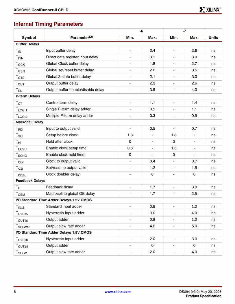
XC2C256 CoolRunner-II CPLDR
(
Internal Timing Parameters
Symbol Parameter(2)
-6 -7
UnitsMin Max Min Max
Buffer Delays
TIN Input buffer delay - 24 - 26 ns
TDIN Direct data register input delay - 31 - 39 ns
TGCK Global Clock buffer delay - 18 - 27 ns
TGSR Global setreset buffer delay - 20 - 35 ns
TGTS Global 3-state buffer delay - 21 - 30 ns
TOUT Output buffer delay - 23 - 26 ns
TEN Output buffer enabledisable delay - 35 - 40 ns
P-term Delays
TCT Control term delay - 11 - 14 ns
TLOGI1 Single P-term delay adder - 05 - 11 ns
TLOGI2 Multiple P-term delay adder - 03 - 05 ns
Macrocell Delay
TPDI Input to output valid - 05 - 07 ns
TSUI Setup before clock 13 - 18 - ns
THI Hold after clock 0 - 0 - ns
TECSU Enable clock setup time 08 - 18 - ns
TECHO Enable clock hold time 0 - 0 - ns
TCOI Clock to output valid - 04 - 07 ns
TAOI Setreset to output valid - 12 - 15 ns
TCDBL Clock doubler delay - 0 - 0 ns
Feedback Delays
TF Feedback delay - 17 - 30 ns
TOEM Macrocell to global OE delay - 17 - 25 ns
IO Standard Time Adder Delays 15V CMOS
TIN15 Standard input adder - 08 - 10 ns
THYS15 Hysteresis input adder - 30 - 40 ns
TOUT15 Output adder - 08 - 10 ns
TSLEW15 Output slew rate adder - 40 - 50 ns
IO Standard Time Adder Delays 18V CMOS
THYS18 Hysteresis input adder - 20 - 30 ns
TOUT18 Output adder - 0 - 0 ns
TSLEW Output slew rate adder - 20 - 40 ns
8 wwwxilinxcom DS094 (v30) May 20 2006Product Specification
XC2C256 CoolRunner-II CPLDR
Switching Characteristics AC Test Circuit
IO Standard Time Adder Delays 25V CMOS
TIN25 Standard input adder - 06 - 07 ns
THYS25 Hysteresis input adder - 15 - 30 ns
TOUT25 Output adder - 08 - 10 ns
TSLEW25 Output slew rate adder - 30 - 40 ns
IO Standard Time Adder Delays 33V CMOSTTL
TIN33 Standard input adder - 05 - 07 ns
THYS33 Hysteresis input adder - 12 - 30 ns
TOUT33 Output adder - 12 - 16 ns
TSLEW33 Output slew rate adder - 30 - 40 ns
IO Standard Time Adder Delays HSTL SSTL
SSTL2-1 Input adder to TIN TDIN TGCK TGSRTGTS - 04 - 10 ns
Output adder to TOUT - -05 - 00 ns
SSTL3-1 Input adder to TIN TDIN TGCK TGSRTGTS - 04 - 10 ns
Output adder to TOUT - -05 - 00 ns
HSTL-1 Input adder to TIN TDIN TGCK TGSRTGTS - 06 - 10 ns
Output adder to TOUT - 0 - 0 ns
Notes 1 15 ns input pin signal risefall
Internal Timing Parameters (Continued)
Symbol Parameter(2)
-6 -7
UnitsMin Max Min Max
Figure 2 Derating Curve for TPD
Number of Outputs Switching
1 2 4 8 1630
40
50
VCC = VCCIO = 18V T = 25oC
T PD
2 (n
s)
55
45
35
DS092_02_092302
Figure 3 AC Load Circuit
R1
VCC
CLR2
Device Under Test
Output Type
LVTTL33
LVCMOS33
LVCMOS25
LVCMOS18
LVCMOS15
CL includes test fixtures and probe capacitance
15 nsec maximum risefall times on inputs
R1
268Ω 275Ω188Ω
1125Ω150Ω
R2
235Ω275Ω188Ω
1125Ω150Ω
CL
35 pF
35 pF
35pF
35pF
35pF
DS ACT 08 14 02
Test Point
DS094 (v30) May 20 2006 wwwxilinxcom 9Product Specification
XC2C256 CoolRunner-II CPLDR
Figure 4 Typical IV Curve for XC2C256
VO (Output Volts) XC256_VoIo_all_020703
IO (
Out
put C
urre
nt m
A)
00
40
10
50
20
30
60
30252015105 35
33V
15V
18V
25V
Iol
10 wwwxilinxcom DS094 (v30) May 20 2006Product Specification
XC2C256 CoolRunner-II CPLDR
11
Pin DescriptionsFunction
BlockMacro-
cell VQ100 CP132 TQ144 PQ208 FT256IO
Bank
1 1 - - - 2 B3 2
1 2 - - - 208 B4 2
1(GSR) 3 99 A3 143 206 C4 2
1 4 - - 142 205 A2 2
1 5 - - - 203 A3 2
1 6 97 B4 140 202 A4 2
1 7 - - - - - -
1 8 - - - - - -
1 9 - - - - - -
1 10 - - - - - -
1 11 - - - - - -
1 12 96 - 139 201 B5 2
1 13 95 - 138 200 A5 2
1 14 94 A4 137 199 E8 2
1 15 - - - 198 B6 2
1 16 - C5 - 197 C7 2
2(GTS2) 1 1 A1 2 3 D3 2
2 2 - - - 4 C3 2
2(GTS3) 3 2 B2 3 5 E3 2
2 4 - B1 4 6 B2 2
2(GTS0) 5 3 C3 5 7 D4 2
2 6 - - - 8 D2 2
2 7 - - - - - -
2 8 - - - - - -
2 9 - - - - - -
2 10 - - - - - -
2 11 - - - - - -
2(GTS1) 12 4 C2 6 9 E5 2
2 13 - C1 7 10 B1 2
2 14 6 D2 9 12 E4 2
2 15 7 - 10 14 C1 2
2 16 - D1 - - E2 2
3 1 - - 136 196 A6 2
3 2 - B5 135 195 D7 2
3 3 - - 134 194 B7 2
3 4 - A5 - 193 E9 2
3 5 93 - 133 192 A7 2
3 6 C6 191 D8 2
3 7 - - - - - -
3 8 - - - - - -
3 9 - - - - - -
3 10 - - - - - -
3 11 - - - - - -
3 12 92 - - 189 B8 2
3 13 - B6 - 188 C8 2
3 14 91 A6 132 187 A8 2
3 15 - C7 - 186 E11 2
3 16 90 B7 131 185 E10 2
4 1 8 E3 11 15 F2 2
4 2 9 - 12 16 F3 2
4 3 10 E2 13 17 G4 2
4 4 - E1 14 18 G3 2
4 5 11 F3 15 19 F5 2
4 6 12 F2 16 20 G5 2
4 7 - - - - - -
4 8 - - - - - -
4 9 - - - - - -
4 10 - - - - - -
4 11 - - - - - -
4 12 - F1 17 21 H2 2
4 13 13 G1 - 22 H4 2
4 14 - - 18 23 H3 2
4 15 - - - - H1 2
4 16 - - - 25 H5 2
Pin Descriptions (Continued)Function
BlockMacro-
cell VQ100 CP132 TQ144 PQ208 FT256IO
Bank
DS094 (v30) May 20 2006 wwwxilinxcom 11Product Specification
XC2C256 CoolRunner-II CPLDR
5 1 - L3 - 49 R1 1
5 2 - - 33 48 N4 1
5 3 - - - 47 N2 1
5(GCK1) 4 23 L2 32 46 M3 1
5 5 L1 31 45 P1 1
5(GCK0) 6 22 K3 30 44 M2 1
5 7 - - - - - -
5 8 - - - - - -
5 9 - - - - - -
5 10 - - - - - -
5 11 - - - - - -
5 12 - - - 43 L3 1
5 13 - - - 41 N1 1
5 14 - - 28 40 L4 1
5 15 - - - 39 M1 1
5 16 - K1 - 38 L5 1
6 1 - M1 34 50 N3 1
6 (CDRST)
2 24 M2 35 51 P2 1
6 3 - - - 54 P4 1
6(GCK2) 4 27 N2 38 55 P5 1
6 5 - - - 56 R2 1
6 6 - - - 57 T1 1
6 7 - - - - - -
6 8 - - - - - -
6 9 - - - - - -
6 10 - - - - - -
6 11 - - - - - -
6(DGE) 12 28 P2 39 58 T2 1
6 13 - M3 40 60 N5 1
6 14 29 N3 41 61 R4 1
6 15 - P3 42 62 M5 1
6 16 30 M4 43 63 R5 1
Pin Descriptions (Continued)Function
BlockMacro-
cell VQ100 CP132 TQ144 PQ208 FT256IO
Bank
7 1 - - - 37 K4 1
7 2 - - - 36 L2 1
7 3 - - - 35 K3 1
7 4 - - - 34 L1 1
7 5 19 J2 26 32 K5 1
7 6 18 J1 25 31 K2 1
7 7 - - - - - -
7 8 - - - - - -
7 9 - - - - - -
7 10 - - - - - -
7 11 17 H3 24 30 J4 1
7 12 16 H2 23 29 K1 1
7 13 15 H1 22 28 J3 1
7 14 14 G3 21 27 J2 1
7 15 - G2 20 - J5 1
7 16 - - 19 - J1 1
8 1 - N4 44 64 R6 1
8 2 - - 45 65 N6 1
8 3 - - 46 66 R3 1
8 4 - - - 67 M6 1
8 5 - - 48 69 T3 1
8 6 32 - 49 70 P6 1
8 7 - - - - - -
8 8 - - - - - -
8 9 - - - - - -
8 10 - - - - - -
8 11 33 M5 50 71 T4 1
8 12 34 N5 51 72 P7 1
8 13 35 P5 52 73 T5 1
8 14 36 M6 - 74 N7 1
8 15 37 N6 - 75 R7 1
8 16 - - - 76 M7 1
Pin Descriptions (Continued)Function
BlockMacro-
cell VQ100 CP132 TQ144 PQ208 FT256IO
Bank
12 wwwxilinxcom DS094 (v30) May 20 2006Product Specification
XC2C256 CoolRunner-II CPLDR
9 1 78 C12 112 160 B13 2
9 2 79 B12 113 161 B14 2
9 3 - - - 162 C13 2
9 4 80 A12 114 163 A15 2
9 5 164 C12 2
9 6 81 C11 115 165 B12 2
9 7 - - - - - -
9 8 - - - - - -
9 9 - - - - - -
9 10 - - - - - -
9 11 - - - 166 D13 2
9 12 82 B11 116 167 A14 2
9 13 - - 117 168 E13 2
9 14 - A11 118 169 A13 2
9 15 - - 119 170 C11 2
9 16 - C10 - 171 A12 2
10 1 77 A13 111 159 A16 2
10 2 76 B13 110 158 B15 2
10 3 74 C13 107 155 C14 2
10 4 73 C14 106 154 G11 2
10 5 72 D12 105 153 B16 2
10 6 71 D13 104 152 D15 2
10 7 - - - - - -
10 8 - - - - - -
10 9 - - - - - -
10 10 - - - - - -
10 11 151 E14 2
10 12 70 D14 103 150 C16 2
10 13 - - - 149 F14 2
10 14 - E12 102 148 F13 2
10 15 - - - 147 E15 2
10 16 - E13 101 146 G13 2
Pin Descriptions (Continued)Function
BlockMacro-
cell VQ100 CP132 TQ144 PQ208 FT256IO
Bank
11 1 - B10 - - B11 2
11 2 - - 173 D11 2
11 3 - A10 - 174 A11 2
11 4 - - - 175 D10 2
11 5 - C9 120 - B10 2
11 6 - - 121 - E12 2
11 7 - - - - - -
11 8 - - - - - -
11 9 - - - - - -
11 10 - - - - - -
11 11 85 A8 124 178 F12 2
11 12 86 B8 125 179 B9 2
11 13 87 C8 126 180 C9 2
11 14 89 - 128 182 C10 2
11 15 - - 129 183 A9 2
11 16 - - 130 184 D9 2
12 1 - - - 145 F15 2
12 2 - - 100 144 G14 2
12 3 - - - 143 E16 2
12 4 - - - 142 H12 2
12 5 - F12 - 140 F16 2
12 6 - F13 - 139 H16 2
12 7 - - - - - -
12 8 - - - - - -
12 9 - - - - - -
12 10 - - - - - -
12 11 68 F14 98 138 G15 2
12 12 - G12 97 137 H13 2
12 13 67 G13 96 136 G16 2
12 14 66 - 95 135 H14 2
12 15 65 - 94 134 H15 2
12 16 - - - - J12 2
Pin Descriptions (Continued)Function
BlockMacro-
cell VQ100 CP132 TQ144 PQ208 FT256IO
Bank
DS094 (v30) May 20 2006 wwwxilinxcom 13Product Specification
XC2C256 CoolRunner-II CPLDR
13 1 - N13 75 107 R15 1
13 2 53 N14 76 108 T16 1
13 3 - M12 77 109 N14 1
13 4 54 - - 110 R16 1
13 5 - M13 78 111 N15 1
13 6 55 - 79 112 M15 1
13 7 - - - - - -
13 8 - - - - - -
13 9 - - - - - -
13 10 - - - - - -
13 11 - - - - - -
13 12 - M14 80 113 M13 1
13 13 56 - 81 114 P16 1
13 14 - L12 82 115 N16 1
13 15 - - - 116 L14 1
13 16 - L13 - 117 M14 1
14 1 52 P14 74 106 P15 1
14 2 - - 71 103 P14 1
14 3 50 P12 70 102 P13 1
14 4 - M11 69 101 R13 1
14 5 49 N11 - 100 N13 1
14 6 - P11 68 - R14 1
14 7 - - - - - -
14 8 - - - - - -
14 9 - - - - - -
14 10 - - - - - -
14 11 - - - - - -
14 12 - - - 99 T15 1
14 13 - - 66 97 R12 1
14 14 46 P10 64 95 N11 1
14 15 44 - - - M11 1
14 16 - P9 61 91 N10 1
Pin Descriptions (Continued)Function
BlockMacro-
cell VQ100 CP132 TQ144 PQ208 FT256IO
Bank
15 1 - - - 118 L15 1
15 2 - L14 83 119 L13 1
15 3 - - - 120 M12 1
15 4 - - - 121 M16 1
15 5 - - - 122 K14 1
15 6 - - - 123 L16 1
15 7 - - - - - -
15 8 - - - - - -
15 9 - - - - - -
15 10 - - - - - -
15 11 58 K13 85 125 K15 1
15 12 59 K14 86 126 L12 1
15 13 60 J12 87 127 K16 1
15 14 61 J13 88 128 J14 1
15 15 63 H13 91 - J15 1
15 16 64 H12 92 131 J13 1
16 1 - - - 90 P10 1
16 2 - - - 89 R10 1
16 3 - M8 - 88 T10 1
16 4 - - - 87 R9 1
16 5 43 N8 60 86 N9 1
16 6 42 - 59 85 M8 1
16 7 - - - - - -
16 8 - - - - - -
16 9 - - - - - -
16 10 - - - - - -
16 11 41 P8 58 84 T8 1
16 12 40 M7 57 83 P8 1
16 13 39 N7 56 82 R8 1
16 14 - - - 80 T7 1
16 15 - - 54 78 N8 1
16 16 - P6 53 77 T6 1
Notes 1 GTS = global output enable GSR = global resetset GCK =
global clock CDRST = clock divide reset DGE = DataGATE enable
2 GTS GSR and GCK pins can be used for general purpose IO
Pin Descriptions (Continued)Function
BlockMacro-
cell VQ100 CP132 TQ144 PQ208 FT256IO
Bank
14 wwwxilinxcom DS094 (v30) May 20 2006Product Specification
XC2C256 CoolRunner-II CPLDR
XC2C256 JTAG PowerGround No Connect Pins and Total User IO
Pin Type VQ100 CP132 TQ144 PQ208 FT256
TCK 48 M10 67 98 P12
TDI 45 M9 63 94 R11
TDO 83 B9 122 176 A10
TMS 47 N10 65 96 N12
VCCAUX (JTAG supply voltage)
5 D3 8 11 F4
Power internal (VCC) 26 57 P1 K12 A2 1 37 84 1 53 124 P3 K13 D12 D5
Power Bank 1 IO (VCCIO1) 20 38 51 J3 P7 G14 P13
27 55 73 93 33 59 79 92 105 132
J6 K6 L7 L8 J11 K11 L10 L9
Power Bank 2 IO (VCCIO2) 88 98 A14 C4 A7 109 127 141 26 133 157 172 181 204
F7 F8 G6 H6 F10 F9 H11
Ground 21 25 31 62 69 75
84 100
K2 N1 P4 N9 N12 J14 H14 E14 B14
A9 B3
29 36 47 62 72 89 90 99 108 123 144
13 24 42 52 68 81 93 104 129 130 141 156 177 190
207
F11 F6 G10 G7 G8 G9 H10 H7 H8 H9 J10 J7 J8 J9 K10 K7 K8 K9 L11 L6
No connects - - - - A1 C2 E6 D1 E1 G2 F1 G1 M4 T9 P9 M9 M10 T11 T12 T13 P11 T14 J16 K12 D16 G12 C15 D14 D6 C6 E7 C5
Total user IO 80 106 118 173 184
DS094 (v30) May 20 2006 wwwxilinxcom 15Product Specification
XC2C256 CoolRunner-II CPLDR
Ordering Information
Part NumberPinBall Spacing
θJA (CWatt)
θJC (CWatt) Package Type
Package Body Dimensions IO
Commercial (C)
Industrial (I)(1)
XC2C256-6VQ100C 05mm 431 109 Very Thin Quad Flat Pack
14mm x 14mm 80 C
XC2C256-7VQ100C 05mm 431 109 Very Thin Quad Flat Pack
14mm x 14mm 80 C
XC2C256-6CP132C 05mm 650 150 Chip Scale Package 8mm x 8mm 106 C
XC2C256-7CP132C 05mm 650 150 Chip Scale Package 8mm x 8mm 106 C
XC2C256-6TQ144C 05mm 372 72 Thin Quad Flat Pack 20mm x 20mm 118 C
XC2C256-7TQ144C 05mm 372 72 Thin Quad Flat Pack 20mm x 20mm 118 C
XC2C256-6PQ208C 05mm 369 97 Plastic Quad Flat Pack
28mm x 28mm 173 C
XC2C256-7PQ208C 05mm 369 97 Plastic Quad Flat Pack
28mm x 28mm 173 C
XC2C256-6FT256C 10mm 346 61 Fine Pitch Thin BGA 17mm x 17mm 184 C
XC2C256-7FT256C 10mm 346 61 Fine Pitch Thin BGA 17mm x 17mm 184 C
XC2C256-6VQG100C 05mm 431 109 Very Thin Quad Flat Pack Pb-free
14mm x 14mm 80 C
XC2C256-7VQG100C 05mm 431 109 Very Thin Quad Flat Pack Pb-free
14mm x 14mm 80 C
XC2C256-6CPG132C 05mm 650 150 Chip Scale Package Pb-free
8mm x 8mm 106 C
XC2C256-7CPG132C 05mm 650 150 Chip Scale Package Pb-free
8mm x 8mm 106 C
XC2C256-6TQG144C 05mm 372 72 Thin Quad Flat Pack Pb-free
20mm x 20mm 118 C
XC2C256-7TQG144C 05mm 372 72 Thin Quad Flat Pack Pb-free
20mm x 20mm 118 C
XC2C256-6PQG208C 05mm 369 97 Plastic Quad Flat Pack Pb-free
28mm x 28mm 173 C
XC2C256-7PQG208C 05mm 369 97 Plastic Quad Flat Pack Pb-free
28mm x 28mm 173 C
XC2C256-6FTG256C 10mm 346 61 Fine Pitch Thin BGA Pb-free
17mm x 17mm 184 C
XC2C256-7FTG256C 10mm 346 61 Fine Pitch Thin BGA Pb-free
17mm x 17mm 184 C
XC2C256-7VQ100I 05mm 431 109 Very Thin Quad Flat Pack
14mm x 14mm 80 I
XC2C256-7CP132I 05mm 650 150 Chip Scale Package 8mm x 8mm 106 I
XC2C256-7TQ144I 05mm 372 72 Thin Quad Flat Pack 20mm x 20mm 118 I
XC2C256-7PQ208I 05mm 369 97 Plastic Quad Flat Pack
28mm x 28mm 173 I
XC2C256-7FT256I 10mm 346 61 Fine Pitch Thin BGA 17mm x 17mm 184 I
16 wwwxilinxcom DS094 (v30) May 20 2006Product Specification
XC2C256 CoolRunner-II CPLDR
Device Part Marking
Figure 5 Sample Package with Part Marking
Note Due to the small size of chip scale packages the complete ordering part number cannot be included on the packagemarking Part marking on chip scale packages by line are
bull Line 1 = X (Xilinx logo) then truncated part numberbull Line 2 = Not related to device part numberbull Line 3 = Not related to device part number
1 Line 4 = Package code speed operating temperature three digits not related to device part number Package codes C5 = CP132 C6 = CPG132
XC2C256-7VQG100I 05mm 431 109 Very Thin Quad Flat Pack Pb-free
14mm x 14mm 80 I
XC2C256-7CPG132I 05mm 650 150 Chip Scale Package Pb-free
8mm x 8mm 106 I
XC2C256-7TQG144I 05mm 372 72 Thin Quad Flat Pack Pb-free
20mm x 20mm 118 I
XC2C256-7PQG208I 05mm 369 97 Plastic Quad Flat Pack Pb-free
28mm x 28mm 173 I
XC2C256-7FTG256I 10mm 346 61 Fine Pitch Thin BGA Pb-free
17mm x 17mm 184 I
Notes 1 C = Commercial (TA = 0degC to +70degC) I = Industrial (TA = ndash40degC to +85degC)
Part NumberPinBall Spacing
θJA (CWatt)
θJC (CWatt) Package Type
Package Body Dimensions IO
Commercial (C)
Industrial (I)(1)
Standard Example XC2C128 Device Speed Grade Package Type Number of Pins Temperature Range
-6 TQ C144 Pb-Free Example XC2C128 TQ G 144 C
Device Speed Grade Package Type Pb-FreeNumber of Pins
-6
Temperature Range
XC2Cxxx
TQ144
7C
Device Type
Package
Speed
Operating Range
This line not
related to device
part number
R
Part marking for non-chip scale package
DS094 (v30) May 20 2006 wwwxilinxcom 17Product Specification
XC2C256 CoolRunner-II CPLDR
Figure 6 VQ100 Very Thin Quad Flat Pack
VQ100Top View
GN
DIO
(3)
VC
CIO
2IO IO IO IO IO IO IO IO IO V
CC
IO2
IO IO IO GN
DT
DO
IO IO IO IO IO IO IO
VC
CIO
(2)
IO(5
)
IO IOG
ND
IO IO IO IO IO IOV
CC
IO1
IO IO IO IO IO IO TD
IIO
TM
ST
CK
IO IO
GNDIOIOIOIOIOGNDIOIOIOIOIOIOGNDIOIOIOIOVCCIOIOIOIOIOVCCIO1
IO(1)IO(1)IO(1)IO(1)VAUX
IOIOIOIOIOIOIOIOIOIOIOIOIOIO
VCCIO1GND
IO(2)IO(2)IO(4)GND
12345678910111213141516171819202122232425
75747372717069686766656463626160595857565554535251
26 27 28 29 30 31 32 33 34 35 36 37 38 39 40 41 42 43 44 45 46 47 48 49 50
100 99 98 97 96 95 94 93 92 91 90 89 88 87 86 85 84 83 82 81 80 79 78 77 76
(1) - Global Output Enable(2) - Global Clock(3) - Global SetReset(4) - Clock Divide Reset(5) - Data Gate
18 wwwxilinxcom DS094 (v30) May 20 2006Product Specification
XC2C256 CoolRunner-II CPLDR
Figure 7 CP132 Chip Scale Package
CP132Bottom View
P
N
M
L
K
J
H
G
F
E
D
C
B
A
1 2 3 4 5 6 7 8 9 10 11 12 13 14
VCC VCCIO1 VCCIO1GNDIO IO IO IO IO IO IO IO IOIO(5)
IO IOVAUX IO IOIO
IO IOIO IO IOIO
IO IOIO IO VCCIO1IO
IO IOIO IO GNDIO
IO IOIO IO GNDIO
IO IOVCCIO1 IO GNDIO
IO IOIO(2) VCC IOGND
IO IOIO IO IOIO(2)
IO(1) VCCIO2 IOIOIO(3) IO IO IO GND IO IO IO VCCIO2VCC
IO IO IOIOGND IO IO IO TDO IO IO IO GNDIO(1)
IO IO IOVCCIO2IO(1) IO IO IO IO IO IO IO IOIO(1)
IO IO IOIOIO IO IO IO TDI TCK IO IO IOIO(4)
GND IO IOIOIO IO IO IO GND TMS IO GND IOIO(2)
(1) - Global Output Enable(2) - Global Clock(3) - Global SetReset(4) - Clock Divide Reset(5) - DataGATE Enable
DS094 (v30) May 20 2006 wwwxilinxcom 19Product Specification
XC2C256 CoolRunner-II CPLDR
Figure 8 TQ144 Thin Quad Flat Pack
VCCIO(1)
IO(1)
IOIO(1)
IO(1)
IOVAUX
IOIOIOIOIOIOIOIOIOIOIOIOIOIOIOIOIOIO
VCCIO1IO
GNDIO(2)
IOIO(2)
IOIO
IO(4)
GND
123456789101112131415161718192021222324252627282930313233343536
TQ144Top View
VC
CIO
(2)
IO(5
)
IO IO IO IO IO IO IOG
ND
IO IO IO IO IO IO IOV
CC
IO1
IO IO IO IO IO IOG
ND
TD
IIO
TM
SIO
TC
KIO IO IO IO
GN
D
108107106105104103102101100999897969594939291908988878685848382818079787776757473
37 38 39 40 41 42 43 44 45 46 47 48 49 50 51 52 53 54 55 56 57 58 59 60 61 62 63 64 65 66 67 68 69 70 71 72
144
143
142
141
140
139
138
137
136
135
134
133
132
131
130
129
128
127
126
125
124
123
122
121
120
119
118
117
116
115
114
113
112
111
110
109
GNDIOIOIOIOIOIOIOIOGNDIOIOIOIOIOVCCIO1IOIOGNDGNDIOIOIOIOVCCIOIOIOIOIOIOIOIOIOIOVCCIO1
GN
DIO
(3)
IO VC
CIO
2IO IO IO IO IO IO IO IO IO IO IO IO IO V
CC
IO2
IO IO IO GN
DT
DO
IO IO IO IO IO IO IO IO IO IO IO IO VC
CIO
2
(1) - Global Output Enable(2) - Global Clock(3) - Global SetReset(4) - Clock Divide Reset(5) - DataGATE Enable
20 wwwxilinxcom DS094 (v30) May 20 2006Product Specification
XC2C256 CoolRunner-II CPLDR
Figure 9 PQ208 Quad Flat Package
VCCIO
IO(1)IO
IO(1)IO
IO(1)IO
IO(1)IO
VAUXIO
GNDIOIOIOIOIOIOIOIOIOIO
GNDIO
VCCIO2IOIOIOIOIOIO
VCCIO1IOIOIOIOIOIOIOIO
GNDIO
IO(2)IO
IO(2)IOIOIOIO
IO(4)GND
PQ208Top View
VC
CI
OI
O(2
)I
OI
OI
O(5
)V
CC
IO1
IO
IO
IO
IO
IO
IO
IO
IO
GN
DI
OI
OI
OI
OI
OI
OI
OI
OI
OI
OV
CC
IO1
IO
GN
DI
OI
OI
OI
OI
OI
OI
OI
OI
OI
OV
CC
IO1
GN
DT
DI
IO
TM
SI
OT
CK
IO
IO
IO
IO
IO
GN
D
(1) - Global Output Enable(2) - Global Clock(3) - Global SetReset(4) - Clock Divide Reset(5) - DataGATE Enable
GNDIOIOIOIOIOIOIOIOIOIOIOIOIOIOGNDIOIOIOIOIOIOIOVCCIO2VCCIO1IOGNDGNDIOIOIOIOVCCIOIOIOIOIOIOIOIOIOIOIOIOIOIOIOIOIOIOVCCIO1
IO GN
DIO
(3)
IO VC
CIO
2IO IO IO IO IO IO IO IO IO IO IO IO IO G
ND
IO IO IO IO IO IO IO IO VC
CIO
2IO IO IO G
ND
TD
OIO IO IO V
CC
IO2
IO IO IO IO IO IO IO IO IO IO IO IO IO IO VC
CIO
2
12345678910111213141516171819202122232425262728293031323334353637383940414243444546474849505152
53 54 55 56 57 58 59 60 61 62 63 64 65 66 67 68 69 70 71 72 73 74 75 76 77 78 79 80 81 82 83 84 85 86 87 88 89 90 91 92 93 94 95 96 97 98 99 100
101
102
103
104
156155154153152151150149148147146145144143142141140139138137136135134133132131130129128127126125124123122121120119118117116115114113112111110109108107106105
208
207
206
205
204
203
202
201
200
199
198
197
196
195
194
193
192
191
190
189
188
187
186
185
184
183
182
181
180
179
178
177
176
175
174
173
172
171
170
169
168
167
166
165
164
163
162
161
160
159
158
157
DS094 (v30) May 20 2006 wwwxilinxcom 21Product Specification
XC2C256 CoolRunner-II CPLDR
Warranty DisclaimerTHESE PRODUCTS ARE SUBJECT TO THE TERMS OF THE XILINX LIMITED WARRANTY WHICH CAN BE VIEWEDAT httpwwwxilinxcomwarrantyhtm THIS LIMITED WARRANTY DOES NOT EXTEND TO ANY USE OF THEPRODUCTS IN AN APPLICATION OR ENVIRONMENT THAT IS NOT WITHIN THE SPECIFICATIONS STATED ON THETHEN-CURRENT XILINX DATA SHEET FOR THE PRODUCTS PRODUCTS ARE NOT DESIGNED TO BE FAIL-SAFEAND ARE NOT WARRANTED FOR USE IN APPLICATIONS THAT POSE A RISK OF PHYSICAL HARM OR LOSS OFLIFE USE OF PRODUCTS IN SUCH APPLICATIONS IS FULLY AT THE RISK OF CUSTOMER SUBJECT TOAPPLICABLE LAWS AND REGULATIONS
Figure 10 FT256 Fine Pitch Thin BGA
FT256 Bottom View
A
B
C
D
E
F
G
H
J
K
L
M
N
P
R
T
16 15 14 13 12 11 10 9 8 7 6 5 4 3 2 1
IO TDO IOIOIO IO IO IO IO IO IO IO IO IO NCIO
IO IO IOIOIO IO IO IO IO IO IO IO IO IO IOIO
IO IO IO(3)IOIO IO IO IO IO IO NC NC IO NC IONC
NC IO IO(1)IONC VCC IO IO IO IO NC VCC IO(1) IO NCIO
IO IO IOIOIO IO IO IO IO NC NC IO(1) IO(1) IO NCIO
IO VCCIO2 VAUXIOIO IO GND VCCIO2 VCCIO2 VCCIO2 GND IO IO IO NCIO
IO GND IOIOIO NC IO GND GND GND VCCIO2 IO IO NC NCIO
IO GND IOIOIO IO VCCIO2 GND GND GND VCCIO2 IO IO IO IOIO
NC GND IOIOIO IO VCCIO1 GND GND GND VCCIO1 IO IO IO IOIO
IO GND IOVCCIO NC VCCIO1 GND GND GND VCCIO1 IO IO IO IOIO
IO VCCIO1 IOIOIO IO GND VCCIO1 VCCIO1 VCCIO1 GND IO IO IO IOIO
IO NC NCIOIO IO IO NC IO IO IO IO IO(2) IO(2) IOIO
IO IO IOIOIO TMS IO IO IO IO IO IO IO IO IOIO
IO IO IOIOIO TCK NC NC IO IO IO IO(2) VCC IO(4) IOIO
IO IO IOIOIO IO TDI IO IO IO IO IO IO IO IOIO
IO IO IONCNC NC NC NC IO IO IO IO IO IO(5) IOIO
(1) - Global Output Enable(2) - Global Clock(3) - Global SetReset(4) - Clock Divide Reset(5) - DataGATE Enable
22 wwwxilinxcom DS094 (v30) May 20 2006Product Specification
XC2C256 CoolRunner-II CPLDR
Additional InformationAdditional information is available for the following CoolRunner-II topics
bull XAPP784 Bulletproof CPLD Design Practicesbull XAPP375 Timing Model bull XAPP376 Logic Engine bull XAPP378 Advanced Features bull XAPP382 IO Characteristics bull XAPP389 Powering CoolRunner-II bull XAPP399 Assigning VREF Pins
To access these and all application notes with their associ-ated reference designs click the following link and scrolldown the page until you find the document you want
CoolRunner-II Data Sheets and Application Notes
Device Packages
Revision HistoryThe following table shows the revision history for this document
Date Version Revision
050902 10 Initial Xilinx release
051302 11 Updated AC Electrical Characteristics and added new parameters
103102 12 Corrected package user IO added Voltage Referenced DC tables
031703 20 Added Characterization numbers for product release and device part marking
040203 21 Updated TSOL max from 260 to 220 Changed ICCSB units from mA to μA
012604 22 Updated Device Part Marking Updated links and Tsol
022604 23 Corrected Theta JC value on XC2C256-7TQ144
080304 24 Pb-free documentation
081904 25 Changes to ICCSB maximum specifications in DC Electrical Characteristics table on page 3
100104 26 Add Asynchronous PresetReset Pulse Width specification to AC Electrical Characteristics
030705 27 Removed -5 speed grade Changes to Table 1 IO Standards
062805 28 Move to Product Specification Change to TIN25 TOUT25 TIN33 and TOUT33 for -7 speed grade
032006 29 Add Warranty Disclaimer Add note to Pin Description table that GTS GSR and GCK pins can be used for general purpose IO
52006 30 Moved TCONFIG specification values from MIN column to MAX column page 7
DS094 (v30) May 20 2006 wwwxilinxcom 23Product Specification
- Features
- Description
- RealDigital Design Technology
- Supported IO Standards
- Absolute Maximum Ratings
- Recommended Operating Conditions
- DC Electrical Characteristics (Over Recommended Operating Conditions)
- LVCMOS 33V and LVTTL 33V DC Voltage Specifications
- LVCMOS 25V DC Voltage Specifications
- LVCMOS 18V DC Voltage Specifications
- LVCMOS 15V DC Voltage Specifications(1)
- Schmitt Trigger Input DC Voltage Specifications
- SSTL2-1 DC Voltage Specifications
- SSTL3-1 DC Voltage Specifications
- HSTL1 DC Voltage Specifications
- AC Electrical Characteristics Over Recommended Operating Conditions
- Internal Timing Parameters
-
- Switching Characteristics
- AC Test Circuit
-
- Pin Descriptions
-
- XC2C256 JTAG PowerGround No Connect Pins and Total User IO
-
- Warranty Disclaimer
- Additional Information
- Revision History
-
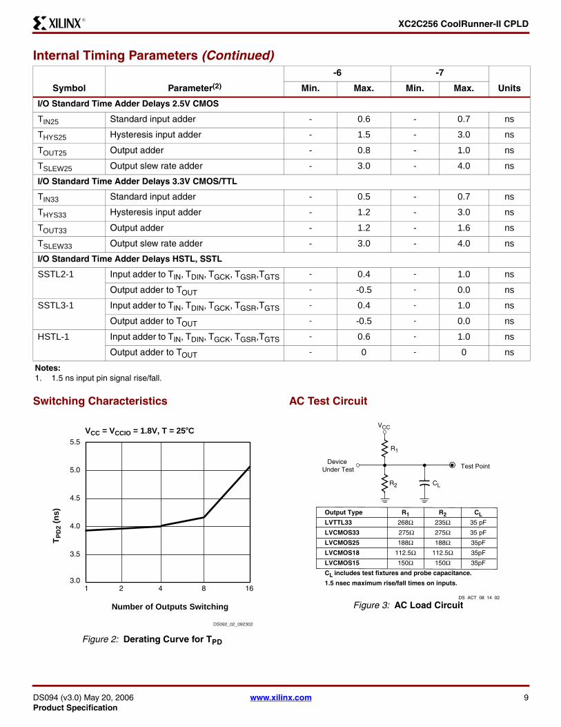
XC2C256 CoolRunner-II CPLDR
Figure 4 Typical IV Curve for XC2C256
VO (Output Volts) XC256_VoIo_all_020703
IO (
Out
put C
urre
nt m
A)
00
40
10
50
20
30
60
30252015105 35
33V
15V
18V
25V
Iol
10 wwwxilinxcom DS094 (v30) May 20 2006Product Specification
XC2C256 CoolRunner-II CPLDR
11
Pin DescriptionsFunction
BlockMacro-
cell VQ100 CP132 TQ144 PQ208 FT256IO
Bank
1 1 - - - 2 B3 2
1 2 - - - 208 B4 2
1(GSR) 3 99 A3 143 206 C4 2
1 4 - - 142 205 A2 2
1 5 - - - 203 A3 2
1 6 97 B4 140 202 A4 2
1 7 - - - - - -
1 8 - - - - - -
1 9 - - - - - -
1 10 - - - - - -
1 11 - - - - - -
1 12 96 - 139 201 B5 2
1 13 95 - 138 200 A5 2
1 14 94 A4 137 199 E8 2
1 15 - - - 198 B6 2
1 16 - C5 - 197 C7 2
2(GTS2) 1 1 A1 2 3 D3 2
2 2 - - - 4 C3 2
2(GTS3) 3 2 B2 3 5 E3 2
2 4 - B1 4 6 B2 2
2(GTS0) 5 3 C3 5 7 D4 2
2 6 - - - 8 D2 2
2 7 - - - - - -
2 8 - - - - - -
2 9 - - - - - -
2 10 - - - - - -
2 11 - - - - - -
2(GTS1) 12 4 C2 6 9 E5 2
2 13 - C1 7 10 B1 2
2 14 6 D2 9 12 E4 2
2 15 7 - 10 14 C1 2
2 16 - D1 - - E2 2
3 1 - - 136 196 A6 2
3 2 - B5 135 195 D7 2
3 3 - - 134 194 B7 2
3 4 - A5 - 193 E9 2
3 5 93 - 133 192 A7 2
3 6 C6 191 D8 2
3 7 - - - - - -
3 8 - - - - - -
3 9 - - - - - -
3 10 - - - - - -
3 11 - - - - - -
3 12 92 - - 189 B8 2
3 13 - B6 - 188 C8 2
3 14 91 A6 132 187 A8 2
3 15 - C7 - 186 E11 2
3 16 90 B7 131 185 E10 2
4 1 8 E3 11 15 F2 2
4 2 9 - 12 16 F3 2
4 3 10 E2 13 17 G4 2
4 4 - E1 14 18 G3 2
4 5 11 F3 15 19 F5 2
4 6 12 F2 16 20 G5 2
4 7 - - - - - -
4 8 - - - - - -
4 9 - - - - - -
4 10 - - - - - -
4 11 - - - - - -
4 12 - F1 17 21 H2 2
4 13 13 G1 - 22 H4 2
4 14 - - 18 23 H3 2
4 15 - - - - H1 2
4 16 - - - 25 H5 2
Pin Descriptions (Continued)Function
BlockMacro-
cell VQ100 CP132 TQ144 PQ208 FT256IO
Bank
DS094 (v30) May 20 2006 wwwxilinxcom 11Product Specification
XC2C256 CoolRunner-II CPLDR
5 1 - L3 - 49 R1 1
5 2 - - 33 48 N4 1
5 3 - - - 47 N2 1
5(GCK1) 4 23 L2 32 46 M3 1
5 5 L1 31 45 P1 1
5(GCK0) 6 22 K3 30 44 M2 1
5 7 - - - - - -
5 8 - - - - - -
5 9 - - - - - -
5 10 - - - - - -
5 11 - - - - - -
5 12 - - - 43 L3 1
5 13 - - - 41 N1 1
5 14 - - 28 40 L4 1
5 15 - - - 39 M1 1
5 16 - K1 - 38 L5 1
6 1 - M1 34 50 N3 1
6 (CDRST)
2 24 M2 35 51 P2 1
6 3 - - - 54 P4 1
6(GCK2) 4 27 N2 38 55 P5 1
6 5 - - - 56 R2 1
6 6 - - - 57 T1 1
6 7 - - - - - -
6 8 - - - - - -
6 9 - - - - - -
6 10 - - - - - -
6 11 - - - - - -
6(DGE) 12 28 P2 39 58 T2 1
6 13 - M3 40 60 N5 1
6 14 29 N3 41 61 R4 1
6 15 - P3 42 62 M5 1
6 16 30 M4 43 63 R5 1
Pin Descriptions (Continued)Function
BlockMacro-
cell VQ100 CP132 TQ144 PQ208 FT256IO
Bank
7 1 - - - 37 K4 1
7 2 - - - 36 L2 1
7 3 - - - 35 K3 1
7 4 - - - 34 L1 1
7 5 19 J2 26 32 K5 1
7 6 18 J1 25 31 K2 1
7 7 - - - - - -
7 8 - - - - - -
7 9 - - - - - -
7 10 - - - - - -
7 11 17 H3 24 30 J4 1
7 12 16 H2 23 29 K1 1
7 13 15 H1 22 28 J3 1
7 14 14 G3 21 27 J2 1
7 15 - G2 20 - J5 1
7 16 - - 19 - J1 1
8 1 - N4 44 64 R6 1
8 2 - - 45 65 N6 1
8 3 - - 46 66 R3 1
8 4 - - - 67 M6 1
8 5 - - 48 69 T3 1
8 6 32 - 49 70 P6 1
8 7 - - - - - -
8 8 - - - - - -
8 9 - - - - - -
8 10 - - - - - -
8 11 33 M5 50 71 T4 1
8 12 34 N5 51 72 P7 1
8 13 35 P5 52 73 T5 1
8 14 36 M6 - 74 N7 1
8 15 37 N6 - 75 R7 1
8 16 - - - 76 M7 1
Pin Descriptions (Continued)Function
BlockMacro-
cell VQ100 CP132 TQ144 PQ208 FT256IO
Bank
12 wwwxilinxcom DS094 (v30) May 20 2006Product Specification
XC2C256 CoolRunner-II CPLDR
9 1 78 C12 112 160 B13 2
9 2 79 B12 113 161 B14 2
9 3 - - - 162 C13 2
9 4 80 A12 114 163 A15 2
9 5 164 C12 2
9 6 81 C11 115 165 B12 2
9 7 - - - - - -
9 8 - - - - - -
9 9 - - - - - -
9 10 - - - - - -
9 11 - - - 166 D13 2
9 12 82 B11 116 167 A14 2
9 13 - - 117 168 E13 2
9 14 - A11 118 169 A13 2
9 15 - - 119 170 C11 2
9 16 - C10 - 171 A12 2
10 1 77 A13 111 159 A16 2
10 2 76 B13 110 158 B15 2
10 3 74 C13 107 155 C14 2
10 4 73 C14 106 154 G11 2
10 5 72 D12 105 153 B16 2
10 6 71 D13 104 152 D15 2
10 7 - - - - - -
10 8 - - - - - -
10 9 - - - - - -
10 10 - - - - - -
10 11 151 E14 2
10 12 70 D14 103 150 C16 2
10 13 - - - 149 F14 2
10 14 - E12 102 148 F13 2
10 15 - - - 147 E15 2
10 16 - E13 101 146 G13 2
Pin Descriptions (Continued)Function
BlockMacro-
cell VQ100 CP132 TQ144 PQ208 FT256IO
Bank
11 1 - B10 - - B11 2
11 2 - - 173 D11 2
11 3 - A10 - 174 A11 2
11 4 - - - 175 D10 2
11 5 - C9 120 - B10 2
11 6 - - 121 - E12 2
11 7 - - - - - -
11 8 - - - - - -
11 9 - - - - - -
11 10 - - - - - -
11 11 85 A8 124 178 F12 2
11 12 86 B8 125 179 B9 2
11 13 87 C8 126 180 C9 2
11 14 89 - 128 182 C10 2
11 15 - - 129 183 A9 2
11 16 - - 130 184 D9 2
12 1 - - - 145 F15 2
12 2 - - 100 144 G14 2
12 3 - - - 143 E16 2
12 4 - - - 142 H12 2
12 5 - F12 - 140 F16 2
12 6 - F13 - 139 H16 2
12 7 - - - - - -
12 8 - - - - - -
12 9 - - - - - -
12 10 - - - - - -
12 11 68 F14 98 138 G15 2
12 12 - G12 97 137 H13 2
12 13 67 G13 96 136 G16 2
12 14 66 - 95 135 H14 2
12 15 65 - 94 134 H15 2
12 16 - - - - J12 2
Pin Descriptions (Continued)Function
BlockMacro-
cell VQ100 CP132 TQ144 PQ208 FT256IO
Bank
DS094 (v30) May 20 2006 wwwxilinxcom 13Product Specification
XC2C256 CoolRunner-II CPLDR
13 1 - N13 75 107 R15 1
13 2 53 N14 76 108 T16 1
13 3 - M12 77 109 N14 1
13 4 54 - - 110 R16 1
13 5 - M13 78 111 N15 1
13 6 55 - 79 112 M15 1
13 7 - - - - - -
13 8 - - - - - -
13 9 - - - - - -
13 10 - - - - - -
13 11 - - - - - -
13 12 - M14 80 113 M13 1
13 13 56 - 81 114 P16 1
13 14 - L12 82 115 N16 1
13 15 - - - 116 L14 1
13 16 - L13 - 117 M14 1
14 1 52 P14 74 106 P15 1
14 2 - - 71 103 P14 1
14 3 50 P12 70 102 P13 1
14 4 - M11 69 101 R13 1
14 5 49 N11 - 100 N13 1
14 6 - P11 68 - R14 1
14 7 - - - - - -
14 8 - - - - - -
14 9 - - - - - -
14 10 - - - - - -
14 11 - - - - - -
14 12 - - - 99 T15 1
14 13 - - 66 97 R12 1
14 14 46 P10 64 95 N11 1
14 15 44 - - - M11 1
14 16 - P9 61 91 N10 1
Pin Descriptions (Continued)Function
BlockMacro-
cell VQ100 CP132 TQ144 PQ208 FT256IO
Bank
15 1 - - - 118 L15 1
15 2 - L14 83 119 L13 1
15 3 - - - 120 M12 1
15 4 - - - 121 M16 1
15 5 - - - 122 K14 1
15 6 - - - 123 L16 1
15 7 - - - - - -
15 8 - - - - - -
15 9 - - - - - -
15 10 - - - - - -
15 11 58 K13 85 125 K15 1
15 12 59 K14 86 126 L12 1
15 13 60 J12 87 127 K16 1
15 14 61 J13 88 128 J14 1
15 15 63 H13 91 - J15 1
15 16 64 H12 92 131 J13 1
16 1 - - - 90 P10 1
16 2 - - - 89 R10 1
16 3 - M8 - 88 T10 1
16 4 - - - 87 R9 1
16 5 43 N8 60 86 N9 1
16 6 42 - 59 85 M8 1
16 7 - - - - - -
16 8 - - - - - -
16 9 - - - - - -
16 10 - - - - - -
16 11 41 P8 58 84 T8 1
16 12 40 M7 57 83 P8 1
16 13 39 N7 56 82 R8 1
16 14 - - - 80 T7 1
16 15 - - 54 78 N8 1
16 16 - P6 53 77 T6 1
Notes 1 GTS = global output enable GSR = global resetset GCK =
global clock CDRST = clock divide reset DGE = DataGATE enable
2 GTS GSR and GCK pins can be used for general purpose IO
Pin Descriptions (Continued)Function
BlockMacro-
cell VQ100 CP132 TQ144 PQ208 FT256IO
Bank
14 wwwxilinxcom DS094 (v30) May 20 2006Product Specification
XC2C256 CoolRunner-II CPLDR
XC2C256 JTAG PowerGround No Connect Pins and Total User IO
Pin Type VQ100 CP132 TQ144 PQ208 FT256
TCK 48 M10 67 98 P12
TDI 45 M9 63 94 R11
TDO 83 B9 122 176 A10
TMS 47 N10 65 96 N12
VCCAUX (JTAG supply voltage)
5 D3 8 11 F4
Power internal (VCC) 26 57 P1 K12 A2 1 37 84 1 53 124 P3 K13 D12 D5
Power Bank 1 IO (VCCIO1) 20 38 51 J3 P7 G14 P13
27 55 73 93 33 59 79 92 105 132
J6 K6 L7 L8 J11 K11 L10 L9
Power Bank 2 IO (VCCIO2) 88 98 A14 C4 A7 109 127 141 26 133 157 172 181 204
F7 F8 G6 H6 F10 F9 H11
Ground 21 25 31 62 69 75
84 100
K2 N1 P4 N9 N12 J14 H14 E14 B14
A9 B3
29 36 47 62 72 89 90 99 108 123 144
13 24 42 52 68 81 93 104 129 130 141 156 177 190
207
F11 F6 G10 G7 G8 G9 H10 H7 H8 H9 J10 J7 J8 J9 K10 K7 K8 K9 L11 L6
No connects - - - - A1 C2 E6 D1 E1 G2 F1 G1 M4 T9 P9 M9 M10 T11 T12 T13 P11 T14 J16 K12 D16 G12 C15 D14 D6 C6 E7 C5
Total user IO 80 106 118 173 184
DS094 (v30) May 20 2006 wwwxilinxcom 15Product Specification
XC2C256 CoolRunner-II CPLDR
Ordering Information
Part NumberPinBall Spacing
θJA (CWatt)
θJC (CWatt) Package Type
Package Body Dimensions IO
Commercial (C)
Industrial (I)(1)
XC2C256-6VQ100C 05mm 431 109 Very Thin Quad Flat Pack
14mm x 14mm 80 C
XC2C256-7VQ100C 05mm 431 109 Very Thin Quad Flat Pack
14mm x 14mm 80 C
XC2C256-6CP132C 05mm 650 150 Chip Scale Package 8mm x 8mm 106 C
XC2C256-7CP132C 05mm 650 150 Chip Scale Package 8mm x 8mm 106 C
XC2C256-6TQ144C 05mm 372 72 Thin Quad Flat Pack 20mm x 20mm 118 C
XC2C256-7TQ144C 05mm 372 72 Thin Quad Flat Pack 20mm x 20mm 118 C
XC2C256-6PQ208C 05mm 369 97 Plastic Quad Flat Pack
28mm x 28mm 173 C
XC2C256-7PQ208C 05mm 369 97 Plastic Quad Flat Pack
28mm x 28mm 173 C
XC2C256-6FT256C 10mm 346 61 Fine Pitch Thin BGA 17mm x 17mm 184 C
XC2C256-7FT256C 10mm 346 61 Fine Pitch Thin BGA 17mm x 17mm 184 C
XC2C256-6VQG100C 05mm 431 109 Very Thin Quad Flat Pack Pb-free
14mm x 14mm 80 C
XC2C256-7VQG100C 05mm 431 109 Very Thin Quad Flat Pack Pb-free
14mm x 14mm 80 C
XC2C256-6CPG132C 05mm 650 150 Chip Scale Package Pb-free
8mm x 8mm 106 C
XC2C256-7CPG132C 05mm 650 150 Chip Scale Package Pb-free
8mm x 8mm 106 C
XC2C256-6TQG144C 05mm 372 72 Thin Quad Flat Pack Pb-free
20mm x 20mm 118 C
XC2C256-7TQG144C 05mm 372 72 Thin Quad Flat Pack Pb-free
20mm x 20mm 118 C
XC2C256-6PQG208C 05mm 369 97 Plastic Quad Flat Pack Pb-free
28mm x 28mm 173 C
XC2C256-7PQG208C 05mm 369 97 Plastic Quad Flat Pack Pb-free
28mm x 28mm 173 C
XC2C256-6FTG256C 10mm 346 61 Fine Pitch Thin BGA Pb-free
17mm x 17mm 184 C
XC2C256-7FTG256C 10mm 346 61 Fine Pitch Thin BGA Pb-free
17mm x 17mm 184 C
XC2C256-7VQ100I 05mm 431 109 Very Thin Quad Flat Pack
14mm x 14mm 80 I
XC2C256-7CP132I 05mm 650 150 Chip Scale Package 8mm x 8mm 106 I
XC2C256-7TQ144I 05mm 372 72 Thin Quad Flat Pack 20mm x 20mm 118 I
XC2C256-7PQ208I 05mm 369 97 Plastic Quad Flat Pack
28mm x 28mm 173 I
XC2C256-7FT256I 10mm 346 61 Fine Pitch Thin BGA 17mm x 17mm 184 I
16 wwwxilinxcom DS094 (v30) May 20 2006Product Specification
XC2C256 CoolRunner-II CPLDR
Device Part Marking
Figure 5 Sample Package with Part Marking
Note Due to the small size of chip scale packages the complete ordering part number cannot be included on the packagemarking Part marking on chip scale packages by line are
bull Line 1 = X (Xilinx logo) then truncated part numberbull Line 2 = Not related to device part numberbull Line 3 = Not related to device part number
1 Line 4 = Package code speed operating temperature three digits not related to device part number Package codes C5 = CP132 C6 = CPG132
XC2C256-7VQG100I 05mm 431 109 Very Thin Quad Flat Pack Pb-free
14mm x 14mm 80 I
XC2C256-7CPG132I 05mm 650 150 Chip Scale Package Pb-free
8mm x 8mm 106 I
XC2C256-7TQG144I 05mm 372 72 Thin Quad Flat Pack Pb-free
20mm x 20mm 118 I
XC2C256-7PQG208I 05mm 369 97 Plastic Quad Flat Pack Pb-free
28mm x 28mm 173 I
XC2C256-7FTG256I 10mm 346 61 Fine Pitch Thin BGA Pb-free
17mm x 17mm 184 I
Notes 1 C = Commercial (TA = 0degC to +70degC) I = Industrial (TA = ndash40degC to +85degC)
Part NumberPinBall Spacing
θJA (CWatt)
θJC (CWatt) Package Type
Package Body Dimensions IO
Commercial (C)
Industrial (I)(1)
Standard Example XC2C128 Device Speed Grade Package Type Number of Pins Temperature Range
-6 TQ C144 Pb-Free Example XC2C128 TQ G 144 C
Device Speed Grade Package Type Pb-FreeNumber of Pins
-6
Temperature Range
XC2Cxxx
TQ144
7C
Device Type
Package
Speed
Operating Range
This line not
related to device
part number
R
Part marking for non-chip scale package
DS094 (v30) May 20 2006 wwwxilinxcom 17Product Specification
XC2C256 CoolRunner-II CPLDR
Figure 6 VQ100 Very Thin Quad Flat Pack
VQ100Top View
GN
DIO
(3)
VC
CIO
2IO IO IO IO IO IO IO IO IO V
CC
IO2
IO IO IO GN
DT
DO
IO IO IO IO IO IO IO
VC
CIO
(2)
IO(5
)
IO IOG
ND
IO IO IO IO IO IOV
CC
IO1
IO IO IO IO IO IO TD
IIO
TM
ST
CK
IO IO
GNDIOIOIOIOIOGNDIOIOIOIOIOIOGNDIOIOIOIOVCCIOIOIOIOIOVCCIO1
IO(1)IO(1)IO(1)IO(1)VAUX
IOIOIOIOIOIOIOIOIOIOIOIOIOIO
VCCIO1GND
IO(2)IO(2)IO(4)GND
12345678910111213141516171819202122232425
75747372717069686766656463626160595857565554535251
26 27 28 29 30 31 32 33 34 35 36 37 38 39 40 41 42 43 44 45 46 47 48 49 50
100 99 98 97 96 95 94 93 92 91 90 89 88 87 86 85 84 83 82 81 80 79 78 77 76
(1) - Global Output Enable(2) - Global Clock(3) - Global SetReset(4) - Clock Divide Reset(5) - Data Gate
18 wwwxilinxcom DS094 (v30) May 20 2006Product Specification
XC2C256 CoolRunner-II CPLDR
Figure 7 CP132 Chip Scale Package
CP132Bottom View
P
N
M
L
K
J
H
G
F
E
D
C
B
A
1 2 3 4 5 6 7 8 9 10 11 12 13 14
VCC VCCIO1 VCCIO1GNDIO IO IO IO IO IO IO IO IOIO(5)
IO IOVAUX IO IOIO
IO IOIO IO IOIO
IO IOIO IO VCCIO1IO
IO IOIO IO GNDIO
IO IOIO IO GNDIO
IO IOVCCIO1 IO GNDIO
IO IOIO(2) VCC IOGND
IO IOIO IO IOIO(2)
IO(1) VCCIO2 IOIOIO(3) IO IO IO GND IO IO IO VCCIO2VCC
IO IO IOIOGND IO IO IO TDO IO IO IO GNDIO(1)
IO IO IOVCCIO2IO(1) IO IO IO IO IO IO IO IOIO(1)
IO IO IOIOIO IO IO IO TDI TCK IO IO IOIO(4)
GND IO IOIOIO IO IO IO GND TMS IO GND IOIO(2)
(1) - Global Output Enable(2) - Global Clock(3) - Global SetReset(4) - Clock Divide Reset(5) - DataGATE Enable
DS094 (v30) May 20 2006 wwwxilinxcom 19Product Specification
XC2C256 CoolRunner-II CPLDR
Figure 8 TQ144 Thin Quad Flat Pack
VCCIO(1)
IO(1)
IOIO(1)
IO(1)
IOVAUX
IOIOIOIOIOIOIOIOIOIOIOIOIOIOIOIOIOIO
VCCIO1IO
GNDIO(2)
IOIO(2)
IOIO
IO(4)
GND
123456789101112131415161718192021222324252627282930313233343536
TQ144Top View
VC
CIO
(2)
IO(5
)
IO IO IO IO IO IO IOG
ND
IO IO IO IO IO IO IOV
CC
IO1
IO IO IO IO IO IOG
ND
TD
IIO
TM
SIO
TC
KIO IO IO IO
GN
D
108107106105104103102101100999897969594939291908988878685848382818079787776757473
37 38 39 40 41 42 43 44 45 46 47 48 49 50 51 52 53 54 55 56 57 58 59 60 61 62 63 64 65 66 67 68 69 70 71 72
144
143
142
141
140
139
138
137
136
135
134
133
132
131
130
129
128
127
126
125
124
123
122
121
120
119
118
117
116
115
114
113
112
111
110
109
GNDIOIOIOIOIOIOIOIOGNDIOIOIOIOIOVCCIO1IOIOGNDGNDIOIOIOIOVCCIOIOIOIOIOIOIOIOIOIOVCCIO1
GN
DIO
(3)
IO VC
CIO
2IO IO IO IO IO IO IO IO IO IO IO IO IO V
CC
IO2
IO IO IO GN
DT
DO
IO IO IO IO IO IO IO IO IO IO IO IO VC
CIO
2
(1) - Global Output Enable(2) - Global Clock(3) - Global SetReset(4) - Clock Divide Reset(5) - DataGATE Enable
20 wwwxilinxcom DS094 (v30) May 20 2006Product Specification
XC2C256 CoolRunner-II CPLDR
Figure 9 PQ208 Quad Flat Package
VCCIO
IO(1)IO
IO(1)IO
IO(1)IO
IO(1)IO
VAUXIO
GNDIOIOIOIOIOIOIOIOIOIO
GNDIO
VCCIO2IOIOIOIOIOIO
VCCIO1IOIOIOIOIOIOIOIO
GNDIO
IO(2)IO
IO(2)IOIOIOIO
IO(4)GND
PQ208Top View
VC
CI
OI
O(2
)I
OI
OI
O(5
)V
CC
IO1
IO
IO
IO
IO
IO
IO
IO
IO
GN
DI
OI
OI
OI
OI
OI
OI
OI
OI
OI
OV
CC
IO1
IO
GN
DI
OI
OI
OI
OI
OI
OI
OI
OI
OI
OV
CC
IO1
GN
DT
DI
IO
TM
SI
OT
CK
IO
IO
IO
IO
IO
GN
D
(1) - Global Output Enable(2) - Global Clock(3) - Global SetReset(4) - Clock Divide Reset(5) - DataGATE Enable
GNDIOIOIOIOIOIOIOIOIOIOIOIOIOIOGNDIOIOIOIOIOIOIOVCCIO2VCCIO1IOGNDGNDIOIOIOIOVCCIOIOIOIOIOIOIOIOIOIOIOIOIOIOIOIOIOIOVCCIO1
IO GN
DIO
(3)
IO VC
CIO
2IO IO IO IO IO IO IO IO IO IO IO IO IO G
ND
IO IO IO IO IO IO IO IO VC
CIO
2IO IO IO G
ND
TD
OIO IO IO V
CC
IO2
IO IO IO IO IO IO IO IO IO IO IO IO IO IO VC
CIO
2
12345678910111213141516171819202122232425262728293031323334353637383940414243444546474849505152
53 54 55 56 57 58 59 60 61 62 63 64 65 66 67 68 69 70 71 72 73 74 75 76 77 78 79 80 81 82 83 84 85 86 87 88 89 90 91 92 93 94 95 96 97 98 99 100
101
102
103
104
156155154153152151150149148147146145144143142141140139138137136135134133132131130129128127126125124123122121120119118117116115114113112111110109108107106105
208
207
206
205
204
203
202
201
200
199
198
197
196
195
194
193
192
191
190
189
188
187
186
185
184
183
182
181
180
179
178
177
176
175
174
173
172
171
170
169
168
167
166
165
164
163
162
161
160
159
158
157
DS094 (v30) May 20 2006 wwwxilinxcom 21Product Specification
XC2C256 CoolRunner-II CPLDR
Warranty DisclaimerTHESE PRODUCTS ARE SUBJECT TO THE TERMS OF THE XILINX LIMITED WARRANTY WHICH CAN BE VIEWEDAT httpwwwxilinxcomwarrantyhtm THIS LIMITED WARRANTY DOES NOT EXTEND TO ANY USE OF THEPRODUCTS IN AN APPLICATION OR ENVIRONMENT THAT IS NOT WITHIN THE SPECIFICATIONS STATED ON THETHEN-CURRENT XILINX DATA SHEET FOR THE PRODUCTS PRODUCTS ARE NOT DESIGNED TO BE FAIL-SAFEAND ARE NOT WARRANTED FOR USE IN APPLICATIONS THAT POSE A RISK OF PHYSICAL HARM OR LOSS OFLIFE USE OF PRODUCTS IN SUCH APPLICATIONS IS FULLY AT THE RISK OF CUSTOMER SUBJECT TOAPPLICABLE LAWS AND REGULATIONS
Figure 10 FT256 Fine Pitch Thin BGA
FT256 Bottom View
A
B
C
D
E
F
G
H
J
K
L
M
N
P
R
T
16 15 14 13 12 11 10 9 8 7 6 5 4 3 2 1
IO TDO IOIOIO IO IO IO IO IO IO IO IO IO NCIO
IO IO IOIOIO IO IO IO IO IO IO IO IO IO IOIO
IO IO IO(3)IOIO IO IO IO IO IO NC NC IO NC IONC
NC IO IO(1)IONC VCC IO IO IO IO NC VCC IO(1) IO NCIO
IO IO IOIOIO IO IO IO IO NC NC IO(1) IO(1) IO NCIO
IO VCCIO2 VAUXIOIO IO GND VCCIO2 VCCIO2 VCCIO2 GND IO IO IO NCIO
IO GND IOIOIO NC IO GND GND GND VCCIO2 IO IO NC NCIO
IO GND IOIOIO IO VCCIO2 GND GND GND VCCIO2 IO IO IO IOIO
NC GND IOIOIO IO VCCIO1 GND GND GND VCCIO1 IO IO IO IOIO
IO GND IOVCCIO NC VCCIO1 GND GND GND VCCIO1 IO IO IO IOIO
IO VCCIO1 IOIOIO IO GND VCCIO1 VCCIO1 VCCIO1 GND IO IO IO IOIO
IO NC NCIOIO IO IO NC IO IO IO IO IO(2) IO(2) IOIO
IO IO IOIOIO TMS IO IO IO IO IO IO IO IO IOIO
IO IO IOIOIO TCK NC NC IO IO IO IO(2) VCC IO(4) IOIO
IO IO IOIOIO IO TDI IO IO IO IO IO IO IO IOIO
IO IO IONCNC NC NC NC IO IO IO IO IO IO(5) IOIO
(1) - Global Output Enable(2) - Global Clock(3) - Global SetReset(4) - Clock Divide Reset(5) - DataGATE Enable
22 wwwxilinxcom DS094 (v30) May 20 2006Product Specification
XC2C256 CoolRunner-II CPLDR
Additional InformationAdditional information is available for the following CoolRunner-II topics
bull XAPP784 Bulletproof CPLD Design Practicesbull XAPP375 Timing Model bull XAPP376 Logic Engine bull XAPP378 Advanced Features bull XAPP382 IO Characteristics bull XAPP389 Powering CoolRunner-II bull XAPP399 Assigning VREF Pins
To access these and all application notes with their associ-ated reference designs click the following link and scrolldown the page until you find the document you want
CoolRunner-II Data Sheets and Application Notes
Device Packages
Revision HistoryThe following table shows the revision history for this document
Date Version Revision
050902 10 Initial Xilinx release
051302 11 Updated AC Electrical Characteristics and added new parameters
103102 12 Corrected package user IO added Voltage Referenced DC tables
031703 20 Added Characterization numbers for product release and device part marking
040203 21 Updated TSOL max from 260 to 220 Changed ICCSB units from mA to μA
012604 22 Updated Device Part Marking Updated links and Tsol
022604 23 Corrected Theta JC value on XC2C256-7TQ144
080304 24 Pb-free documentation
081904 25 Changes to ICCSB maximum specifications in DC Electrical Characteristics table on page 3
100104 26 Add Asynchronous PresetReset Pulse Width specification to AC Electrical Characteristics
030705 27 Removed -5 speed grade Changes to Table 1 IO Standards
062805 28 Move to Product Specification Change to TIN25 TOUT25 TIN33 and TOUT33 for -7 speed grade
032006 29 Add Warranty Disclaimer Add note to Pin Description table that GTS GSR and GCK pins can be used for general purpose IO
52006 30 Moved TCONFIG specification values from MIN column to MAX column page 7
DS094 (v30) May 20 2006 wwwxilinxcom 23Product Specification
- Features
- Description
- RealDigital Design Technology
- Supported IO Standards
- Absolute Maximum Ratings
- Recommended Operating Conditions
- DC Electrical Characteristics (Over Recommended Operating Conditions)
- LVCMOS 33V and LVTTL 33V DC Voltage Specifications
- LVCMOS 25V DC Voltage Specifications
- LVCMOS 18V DC Voltage Specifications
- LVCMOS 15V DC Voltage Specifications(1)
- Schmitt Trigger Input DC Voltage Specifications
- SSTL2-1 DC Voltage Specifications
- SSTL3-1 DC Voltage Specifications
- HSTL1 DC Voltage Specifications
- AC Electrical Characteristics Over Recommended Operating Conditions
- Internal Timing Parameters
-
- Switching Characteristics
- AC Test Circuit
-
- Pin Descriptions
-
- XC2C256 JTAG PowerGround No Connect Pins and Total User IO
-
- Warranty Disclaimer
- Additional Information
- Revision History
-
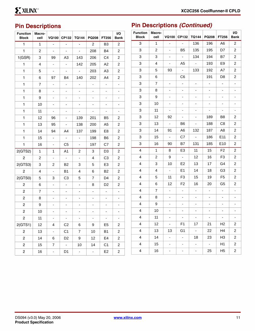
XC2C256 CoolRunner-II CPLDR
11
Pin DescriptionsFunction
BlockMacro-
cell VQ100 CP132 TQ144 PQ208 FT256IO
Bank
1 1 - - - 2 B3 2
1 2 - - - 208 B4 2
1(GSR) 3 99 A3 143 206 C4 2
1 4 - - 142 205 A2 2
1 5 - - - 203 A3 2
1 6 97 B4 140 202 A4 2
1 7 - - - - - -
1 8 - - - - - -
1 9 - - - - - -
1 10 - - - - - -
1 11 - - - - - -
1 12 96 - 139 201 B5 2
1 13 95 - 138 200 A5 2
1 14 94 A4 137 199 E8 2
1 15 - - - 198 B6 2
1 16 - C5 - 197 C7 2
2(GTS2) 1 1 A1 2 3 D3 2
2 2 - - - 4 C3 2
2(GTS3) 3 2 B2 3 5 E3 2
2 4 - B1 4 6 B2 2
2(GTS0) 5 3 C3 5 7 D4 2
2 6 - - - 8 D2 2
2 7 - - - - - -
2 8 - - - - - -
2 9 - - - - - -
2 10 - - - - - -
2 11 - - - - - -
2(GTS1) 12 4 C2 6 9 E5 2
2 13 - C1 7 10 B1 2
2 14 6 D2 9 12 E4 2
2 15 7 - 10 14 C1 2
2 16 - D1 - - E2 2
3 1 - - 136 196 A6 2
3 2 - B5 135 195 D7 2
3 3 - - 134 194 B7 2
3 4 - A5 - 193 E9 2
3 5 93 - 133 192 A7 2
3 6 C6 191 D8 2
3 7 - - - - - -
3 8 - - - - - -
3 9 - - - - - -
3 10 - - - - - -
3 11 - - - - - -
3 12 92 - - 189 B8 2
3 13 - B6 - 188 C8 2
3 14 91 A6 132 187 A8 2
3 15 - C7 - 186 E11 2
3 16 90 B7 131 185 E10 2
4 1 8 E3 11 15 F2 2
4 2 9 - 12 16 F3 2
4 3 10 E2 13 17 G4 2
4 4 - E1 14 18 G3 2
4 5 11 F3 15 19 F5 2
4 6 12 F2 16 20 G5 2
4 7 - - - - - -
4 8 - - - - - -
4 9 - - - - - -
4 10 - - - - - -
4 11 - - - - - -
4 12 - F1 17 21 H2 2
4 13 13 G1 - 22 H4 2
4 14 - - 18 23 H3 2
4 15 - - - - H1 2
4 16 - - - 25 H5 2
Pin Descriptions (Continued)Function
BlockMacro-
cell VQ100 CP132 TQ144 PQ208 FT256IO
Bank
DS094 (v30) May 20 2006 wwwxilinxcom 11Product Specification
XC2C256 CoolRunner-II CPLDR
5 1 - L3 - 49 R1 1
5 2 - - 33 48 N4 1
5 3 - - - 47 N2 1
5(GCK1) 4 23 L2 32 46 M3 1
5 5 L1 31 45 P1 1
5(GCK0) 6 22 K3 30 44 M2 1
5 7 - - - - - -
5 8 - - - - - -
5 9 - - - - - -
5 10 - - - - - -
5 11 - - - - - -
5 12 - - - 43 L3 1
5 13 - - - 41 N1 1
5 14 - - 28 40 L4 1
5 15 - - - 39 M1 1
5 16 - K1 - 38 L5 1
6 1 - M1 34 50 N3 1
6 (CDRST)
2 24 M2 35 51 P2 1
6 3 - - - 54 P4 1
6(GCK2) 4 27 N2 38 55 P5 1
6 5 - - - 56 R2 1
6 6 - - - 57 T1 1
6 7 - - - - - -
6 8 - - - - - -
6 9 - - - - - -
6 10 - - - - - -
6 11 - - - - - -
6(DGE) 12 28 P2 39 58 T2 1
6 13 - M3 40 60 N5 1
6 14 29 N3 41 61 R4 1
6 15 - P3 42 62 M5 1
6 16 30 M4 43 63 R5 1
Pin Descriptions (Continued)Function
BlockMacro-
cell VQ100 CP132 TQ144 PQ208 FT256IO
Bank
7 1 - - - 37 K4 1
7 2 - - - 36 L2 1
7 3 - - - 35 K3 1
7 4 - - - 34 L1 1
7 5 19 J2 26 32 K5 1
7 6 18 J1 25 31 K2 1
7 7 - - - - - -
7 8 - - - - - -
7 9 - - - - - -
7 10 - - - - - -
7 11 17 H3 24 30 J4 1
7 12 16 H2 23 29 K1 1
7 13 15 H1 22 28 J3 1
7 14 14 G3 21 27 J2 1
7 15 - G2 20 - J5 1
7 16 - - 19 - J1 1
8 1 - N4 44 64 R6 1
8 2 - - 45 65 N6 1
8 3 - - 46 66 R3 1
8 4 - - - 67 M6 1
8 5 - - 48 69 T3 1
8 6 32 - 49 70 P6 1
8 7 - - - - - -
8 8 - - - - - -
8 9 - - - - - -
8 10 - - - - - -
8 11 33 M5 50 71 T4 1
8 12 34 N5 51 72 P7 1
8 13 35 P5 52 73 T5 1
8 14 36 M6 - 74 N7 1
8 15 37 N6 - 75 R7 1
8 16 - - - 76 M7 1
Pin Descriptions (Continued)Function
BlockMacro-
cell VQ100 CP132 TQ144 PQ208 FT256IO
Bank
12 wwwxilinxcom DS094 (v30) May 20 2006Product Specification
XC2C256 CoolRunner-II CPLDR
9 1 78 C12 112 160 B13 2
9 2 79 B12 113 161 B14 2
9 3 - - - 162 C13 2
9 4 80 A12 114 163 A15 2
9 5 164 C12 2
9 6 81 C11 115 165 B12 2
9 7 - - - - - -
9 8 - - - - - -
9 9 - - - - - -
9 10 - - - - - -
9 11 - - - 166 D13 2
9 12 82 B11 116 167 A14 2
9 13 - - 117 168 E13 2
9 14 - A11 118 169 A13 2
9 15 - - 119 170 C11 2
9 16 - C10 - 171 A12 2
10 1 77 A13 111 159 A16 2
10 2 76 B13 110 158 B15 2
10 3 74 C13 107 155 C14 2
10 4 73 C14 106 154 G11 2
10 5 72 D12 105 153 B16 2
10 6 71 D13 104 152 D15 2
10 7 - - - - - -
10 8 - - - - - -
10 9 - - - - - -
10 10 - - - - - -
10 11 151 E14 2
10 12 70 D14 103 150 C16 2
10 13 - - - 149 F14 2
10 14 - E12 102 148 F13 2
10 15 - - - 147 E15 2
10 16 - E13 101 146 G13 2
Pin Descriptions (Continued)Function
BlockMacro-
cell VQ100 CP132 TQ144 PQ208 FT256IO
Bank
11 1 - B10 - - B11 2
11 2 - - 173 D11 2
11 3 - A10 - 174 A11 2
11 4 - - - 175 D10 2
11 5 - C9 120 - B10 2
11 6 - - 121 - E12 2
11 7 - - - - - -
11 8 - - - - - -
11 9 - - - - - -
11 10 - - - - - -
11 11 85 A8 124 178 F12 2
11 12 86 B8 125 179 B9 2
11 13 87 C8 126 180 C9 2
11 14 89 - 128 182 C10 2
11 15 - - 129 183 A9 2
11 16 - - 130 184 D9 2
12 1 - - - 145 F15 2
12 2 - - 100 144 G14 2
12 3 - - - 143 E16 2
12 4 - - - 142 H12 2
12 5 - F12 - 140 F16 2
12 6 - F13 - 139 H16 2
12 7 - - - - - -
12 8 - - - - - -
12 9 - - - - - -
12 10 - - - - - -
12 11 68 F14 98 138 G15 2
12 12 - G12 97 137 H13 2
12 13 67 G13 96 136 G16 2
12 14 66 - 95 135 H14 2
12 15 65 - 94 134 H15 2
12 16 - - - - J12 2
Pin Descriptions (Continued)Function
BlockMacro-
cell VQ100 CP132 TQ144 PQ208 FT256IO
Bank
DS094 (v30) May 20 2006 wwwxilinxcom 13Product Specification
XC2C256 CoolRunner-II CPLDR
13 1 - N13 75 107 R15 1
13 2 53 N14 76 108 T16 1
13 3 - M12 77 109 N14 1
13 4 54 - - 110 R16 1
13 5 - M13 78 111 N15 1
13 6 55 - 79 112 M15 1
13 7 - - - - - -
13 8 - - - - - -
13 9 - - - - - -
13 10 - - - - - -
13 11 - - - - - -
13 12 - M14 80 113 M13 1
13 13 56 - 81 114 P16 1
13 14 - L12 82 115 N16 1
13 15 - - - 116 L14 1
13 16 - L13 - 117 M14 1
14 1 52 P14 74 106 P15 1
14 2 - - 71 103 P14 1
14 3 50 P12 70 102 P13 1
14 4 - M11 69 101 R13 1
14 5 49 N11 - 100 N13 1
14 6 - P11 68 - R14 1
14 7 - - - - - -
14 8 - - - - - -
14 9 - - - - - -
14 10 - - - - - -
14 11 - - - - - -
14 12 - - - 99 T15 1
14 13 - - 66 97 R12 1
14 14 46 P10 64 95 N11 1
14 15 44 - - - M11 1
14 16 - P9 61 91 N10 1
Pin Descriptions (Continued)Function
BlockMacro-
cell VQ100 CP132 TQ144 PQ208 FT256IO
Bank
15 1 - - - 118 L15 1
15 2 - L14 83 119 L13 1
15 3 - - - 120 M12 1
15 4 - - - 121 M16 1
15 5 - - - 122 K14 1
15 6 - - - 123 L16 1
15 7 - - - - - -
15 8 - - - - - -
15 9 - - - - - -
15 10 - - - - - -
15 11 58 K13 85 125 K15 1
15 12 59 K14 86 126 L12 1
15 13 60 J12 87 127 K16 1
15 14 61 J13 88 128 J14 1
15 15 63 H13 91 - J15 1
15 16 64 H12 92 131 J13 1
16 1 - - - 90 P10 1
16 2 - - - 89 R10 1
16 3 - M8 - 88 T10 1
16 4 - - - 87 R9 1
16 5 43 N8 60 86 N9 1
16 6 42 - 59 85 M8 1
16 7 - - - - - -
16 8 - - - - - -
16 9 - - - - - -
16 10 - - - - - -
16 11 41 P8 58 84 T8 1
16 12 40 M7 57 83 P8 1
16 13 39 N7 56 82 R8 1
16 14 - - - 80 T7 1
16 15 - - 54 78 N8 1
16 16 - P6 53 77 T6 1
Notes 1 GTS = global output enable GSR = global resetset GCK =
global clock CDRST = clock divide reset DGE = DataGATE enable
2 GTS GSR and GCK pins can be used for general purpose IO
Pin Descriptions (Continued)Function
BlockMacro-
cell VQ100 CP132 TQ144 PQ208 FT256IO
Bank
14 wwwxilinxcom DS094 (v30) May 20 2006Product Specification
XC2C256 CoolRunner-II CPLDR
XC2C256 JTAG PowerGround No Connect Pins and Total User IO
Pin Type VQ100 CP132 TQ144 PQ208 FT256
TCK 48 M10 67 98 P12
TDI 45 M9 63 94 R11
TDO 83 B9 122 176 A10
TMS 47 N10 65 96 N12
VCCAUX (JTAG supply voltage)
5 D3 8 11 F4
Power internal (VCC) 26 57 P1 K12 A2 1 37 84 1 53 124 P3 K13 D12 D5
Power Bank 1 IO (VCCIO1) 20 38 51 J3 P7 G14 P13
27 55 73 93 33 59 79 92 105 132
J6 K6 L7 L8 J11 K11 L10 L9
Power Bank 2 IO (VCCIO2) 88 98 A14 C4 A7 109 127 141 26 133 157 172 181 204
F7 F8 G6 H6 F10 F9 H11
Ground 21 25 31 62 69 75
84 100
K2 N1 P4 N9 N12 J14 H14 E14 B14
A9 B3
29 36 47 62 72 89 90 99 108 123 144
13 24 42 52 68 81 93 104 129 130 141 156 177 190
207
F11 F6 G10 G7 G8 G9 H10 H7 H8 H9 J10 J7 J8 J9 K10 K7 K8 K9 L11 L6
No connects - - - - A1 C2 E6 D1 E1 G2 F1 G1 M4 T9 P9 M9 M10 T11 T12 T13 P11 T14 J16 K12 D16 G12 C15 D14 D6 C6 E7 C5
Total user IO 80 106 118 173 184
DS094 (v30) May 20 2006 wwwxilinxcom 15Product Specification
XC2C256 CoolRunner-II CPLDR
Ordering Information
Part NumberPinBall Spacing
θJA (CWatt)
θJC (CWatt) Package Type
Package Body Dimensions IO
Commercial (C)
Industrial (I)(1)
XC2C256-6VQ100C 05mm 431 109 Very Thin Quad Flat Pack
14mm x 14mm 80 C
XC2C256-7VQ100C 05mm 431 109 Very Thin Quad Flat Pack
14mm x 14mm 80 C
XC2C256-6CP132C 05mm 650 150 Chip Scale Package 8mm x 8mm 106 C
XC2C256-7CP132C 05mm 650 150 Chip Scale Package 8mm x 8mm 106 C
XC2C256-6TQ144C 05mm 372 72 Thin Quad Flat Pack 20mm x 20mm 118 C
XC2C256-7TQ144C 05mm 372 72 Thin Quad Flat Pack 20mm x 20mm 118 C
XC2C256-6PQ208C 05mm 369 97 Plastic Quad Flat Pack
28mm x 28mm 173 C
XC2C256-7PQ208C 05mm 369 97 Plastic Quad Flat Pack
28mm x 28mm 173 C
XC2C256-6FT256C 10mm 346 61 Fine Pitch Thin BGA 17mm x 17mm 184 C
XC2C256-7FT256C 10mm 346 61 Fine Pitch Thin BGA 17mm x 17mm 184 C
XC2C256-6VQG100C 05mm 431 109 Very Thin Quad Flat Pack Pb-free
14mm x 14mm 80 C
XC2C256-7VQG100C 05mm 431 109 Very Thin Quad Flat Pack Pb-free
14mm x 14mm 80 C
XC2C256-6CPG132C 05mm 650 150 Chip Scale Package Pb-free
8mm x 8mm 106 C
XC2C256-7CPG132C 05mm 650 150 Chip Scale Package Pb-free
8mm x 8mm 106 C
XC2C256-6TQG144C 05mm 372 72 Thin Quad Flat Pack Pb-free
20mm x 20mm 118 C
XC2C256-7TQG144C 05mm 372 72 Thin Quad Flat Pack Pb-free
20mm x 20mm 118 C
XC2C256-6PQG208C 05mm 369 97 Plastic Quad Flat Pack Pb-free
28mm x 28mm 173 C
XC2C256-7PQG208C 05mm 369 97 Plastic Quad Flat Pack Pb-free
28mm x 28mm 173 C
XC2C256-6FTG256C 10mm 346 61 Fine Pitch Thin BGA Pb-free
17mm x 17mm 184 C
XC2C256-7FTG256C 10mm 346 61 Fine Pitch Thin BGA Pb-free
17mm x 17mm 184 C
XC2C256-7VQ100I 05mm 431 109 Very Thin Quad Flat Pack
14mm x 14mm 80 I
XC2C256-7CP132I 05mm 650 150 Chip Scale Package 8mm x 8mm 106 I
XC2C256-7TQ144I 05mm 372 72 Thin Quad Flat Pack 20mm x 20mm 118 I
XC2C256-7PQ208I 05mm 369 97 Plastic Quad Flat Pack
28mm x 28mm 173 I
XC2C256-7FT256I 10mm 346 61 Fine Pitch Thin BGA 17mm x 17mm 184 I
16 wwwxilinxcom DS094 (v30) May 20 2006Product Specification
XC2C256 CoolRunner-II CPLDR
Device Part Marking
Figure 5 Sample Package with Part Marking
Note Due to the small size of chip scale packages the complete ordering part number cannot be included on the packagemarking Part marking on chip scale packages by line are
bull Line 1 = X (Xilinx logo) then truncated part numberbull Line 2 = Not related to device part numberbull Line 3 = Not related to device part number
1 Line 4 = Package code speed operating temperature three digits not related to device part number Package codes C5 = CP132 C6 = CPG132
XC2C256-7VQG100I 05mm 431 109 Very Thin Quad Flat Pack Pb-free
14mm x 14mm 80 I
XC2C256-7CPG132I 05mm 650 150 Chip Scale Package Pb-free
8mm x 8mm 106 I
XC2C256-7TQG144I 05mm 372 72 Thin Quad Flat Pack Pb-free
20mm x 20mm 118 I
XC2C256-7PQG208I 05mm 369 97 Plastic Quad Flat Pack Pb-free
28mm x 28mm 173 I
XC2C256-7FTG256I 10mm 346 61 Fine Pitch Thin BGA Pb-free
17mm x 17mm 184 I
Notes 1 C = Commercial (TA = 0degC to +70degC) I = Industrial (TA = ndash40degC to +85degC)
Part NumberPinBall Spacing
θJA (CWatt)
θJC (CWatt) Package Type
Package Body Dimensions IO
Commercial (C)
Industrial (I)(1)
Standard Example XC2C128 Device Speed Grade Package Type Number of Pins Temperature Range
-6 TQ C144 Pb-Free Example XC2C128 TQ G 144 C
Device Speed Grade Package Type Pb-FreeNumber of Pins
-6
Temperature Range
XC2Cxxx
TQ144
7C
Device Type
Package
Speed
Operating Range
This line not
related to device
part number
R
Part marking for non-chip scale package
DS094 (v30) May 20 2006 wwwxilinxcom 17Product Specification
XC2C256 CoolRunner-II CPLDR
Figure 6 VQ100 Very Thin Quad Flat Pack
VQ100Top View
GN
DIO
(3)
VC
CIO
2IO IO IO IO IO IO IO IO IO V
CC
IO2
IO IO IO GN
DT
DO
IO IO IO IO IO IO IO
VC
CIO
(2)
IO(5
)
IO IOG
ND
IO IO IO IO IO IOV
CC
IO1
IO IO IO IO IO IO TD
IIO
TM
ST
CK
IO IO
GNDIOIOIOIOIOGNDIOIOIOIOIOIOGNDIOIOIOIOVCCIOIOIOIOIOVCCIO1
IO(1)IO(1)IO(1)IO(1)VAUX
IOIOIOIOIOIOIOIOIOIOIOIOIOIO
VCCIO1GND
IO(2)IO(2)IO(4)GND
12345678910111213141516171819202122232425
75747372717069686766656463626160595857565554535251
26 27 28 29 30 31 32 33 34 35 36 37 38 39 40 41 42 43 44 45 46 47 48 49 50
100 99 98 97 96 95 94 93 92 91 90 89 88 87 86 85 84 83 82 81 80 79 78 77 76
(1) - Global Output Enable(2) - Global Clock(3) - Global SetReset(4) - Clock Divide Reset(5) - Data Gate
18 wwwxilinxcom DS094 (v30) May 20 2006Product Specification
XC2C256 CoolRunner-II CPLDR
Figure 7 CP132 Chip Scale Package
CP132Bottom View
P
N
M
L
K
J
H
G
F
E
D
C
B
A
1 2 3 4 5 6 7 8 9 10 11 12 13 14
VCC VCCIO1 VCCIO1GNDIO IO IO IO IO IO IO IO IOIO(5)
IO IOVAUX IO IOIO
IO IOIO IO IOIO
IO IOIO IO VCCIO1IO
IO IOIO IO GNDIO
IO IOIO IO GNDIO
IO IOVCCIO1 IO GNDIO
IO IOIO(2) VCC IOGND
IO IOIO IO IOIO(2)
IO(1) VCCIO2 IOIOIO(3) IO IO IO GND IO IO IO VCCIO2VCC
IO IO IOIOGND IO IO IO TDO IO IO IO GNDIO(1)
IO IO IOVCCIO2IO(1) IO IO IO IO IO IO IO IOIO(1)
IO IO IOIOIO IO IO IO TDI TCK IO IO IOIO(4)
GND IO IOIOIO IO IO IO GND TMS IO GND IOIO(2)
(1) - Global Output Enable(2) - Global Clock(3) - Global SetReset(4) - Clock Divide Reset(5) - DataGATE Enable
DS094 (v30) May 20 2006 wwwxilinxcom 19Product Specification
XC2C256 CoolRunner-II CPLDR
Figure 8 TQ144 Thin Quad Flat Pack
VCCIO(1)
IO(1)
IOIO(1)
IO(1)
IOVAUX
IOIOIOIOIOIOIOIOIOIOIOIOIOIOIOIOIOIO
VCCIO1IO
GNDIO(2)
IOIO(2)
IOIO
IO(4)
GND
123456789101112131415161718192021222324252627282930313233343536
TQ144Top View
VC
CIO
(2)
IO(5
)
IO IO IO IO IO IO IOG
ND
IO IO IO IO IO IO IOV
CC
IO1
IO IO IO IO IO IOG
ND
TD
IIO
TM
SIO
TC
KIO IO IO IO
GN
D
108107106105104103102101100999897969594939291908988878685848382818079787776757473
37 38 39 40 41 42 43 44 45 46 47 48 49 50 51 52 53 54 55 56 57 58 59 60 61 62 63 64 65 66 67 68 69 70 71 72
144
143
142
141
140
139
138
137
136
135
134
133
132
131
130
129
128
127
126
125
124
123
122
121
120
119
118
117
116
115
114
113
112
111
110
109
GNDIOIOIOIOIOIOIOIOGNDIOIOIOIOIOVCCIO1IOIOGNDGNDIOIOIOIOVCCIOIOIOIOIOIOIOIOIOIOVCCIO1
GN
DIO
(3)
IO VC
CIO
2IO IO IO IO IO IO IO IO IO IO IO IO IO V
CC
IO2
IO IO IO GN
DT
DO
IO IO IO IO IO IO IO IO IO IO IO IO VC
CIO
2
(1) - Global Output Enable(2) - Global Clock(3) - Global SetReset(4) - Clock Divide Reset(5) - DataGATE Enable
20 wwwxilinxcom DS094 (v30) May 20 2006Product Specification
XC2C256 CoolRunner-II CPLDR
Figure 9 PQ208 Quad Flat Package
VCCIO
IO(1)IO
IO(1)IO
IO(1)IO
IO(1)IO
VAUXIO
GNDIOIOIOIOIOIOIOIOIOIO
GNDIO
VCCIO2IOIOIOIOIOIO
VCCIO1IOIOIOIOIOIOIOIO
GNDIO
IO(2)IO
IO(2)IOIOIOIO
IO(4)GND
PQ208Top View
VC
CI
OI
O(2
)I
OI
OI
O(5
)V
CC
IO1
IO
IO
IO
IO
IO
IO
IO
IO
GN
DI
OI
OI
OI
OI
OI
OI
OI
OI
OI
OV
CC
IO1
IO
GN
DI
OI
OI
OI
OI
OI
OI
OI
OI
OI
OV
CC
IO1
GN
DT
DI
IO
TM
SI
OT
CK
IO
IO
IO
IO
IO
GN
D
(1) - Global Output Enable(2) - Global Clock(3) - Global SetReset(4) - Clock Divide Reset(5) - DataGATE Enable
GNDIOIOIOIOIOIOIOIOIOIOIOIOIOIOGNDIOIOIOIOIOIOIOVCCIO2VCCIO1IOGNDGNDIOIOIOIOVCCIOIOIOIOIOIOIOIOIOIOIOIOIOIOIOIOIOIOVCCIO1
IO GN
DIO
(3)
IO VC
CIO
2IO IO IO IO IO IO IO IO IO IO IO IO IO G
ND
IO IO IO IO IO IO IO IO VC
CIO
2IO IO IO G
ND
TD
OIO IO IO V
CC
IO2
IO IO IO IO IO IO IO IO IO IO IO IO IO IO VC
CIO
2
12345678910111213141516171819202122232425262728293031323334353637383940414243444546474849505152
53 54 55 56 57 58 59 60 61 62 63 64 65 66 67 68 69 70 71 72 73 74 75 76 77 78 79 80 81 82 83 84 85 86 87 88 89 90 91 92 93 94 95 96 97 98 99 100
101
102
103
104
156155154153152151150149148147146145144143142141140139138137136135134133132131130129128127126125124123122121120119118117116115114113112111110109108107106105
208
207
206
205
204
203
202
201
200
199
198
197
196
195
194
193
192
191
190
189
188
187
186
185
184
183
182
181
180
179
178
177
176
175
174
173
172
171
170
169
168
167
166
165
164
163
162
161
160
159
158
157
DS094 (v30) May 20 2006 wwwxilinxcom 21Product Specification
XC2C256 CoolRunner-II CPLDR
Warranty DisclaimerTHESE PRODUCTS ARE SUBJECT TO THE TERMS OF THE XILINX LIMITED WARRANTY WHICH CAN BE VIEWEDAT httpwwwxilinxcomwarrantyhtm THIS LIMITED WARRANTY DOES NOT EXTEND TO ANY USE OF THEPRODUCTS IN AN APPLICATION OR ENVIRONMENT THAT IS NOT WITHIN THE SPECIFICATIONS STATED ON THETHEN-CURRENT XILINX DATA SHEET FOR THE PRODUCTS PRODUCTS ARE NOT DESIGNED TO BE FAIL-SAFEAND ARE NOT WARRANTED FOR USE IN APPLICATIONS THAT POSE A RISK OF PHYSICAL HARM OR LOSS OFLIFE USE OF PRODUCTS IN SUCH APPLICATIONS IS FULLY AT THE RISK OF CUSTOMER SUBJECT TOAPPLICABLE LAWS AND REGULATIONS
Figure 10 FT256 Fine Pitch Thin BGA
FT256 Bottom View
A
B
C
D
E
F
G
H
J
K
L
M
N
P
R
T
16 15 14 13 12 11 10 9 8 7 6 5 4 3 2 1
IO TDO IOIOIO IO IO IO IO IO IO IO IO IO NCIO
IO IO IOIOIO IO IO IO IO IO IO IO IO IO IOIO
IO IO IO(3)IOIO IO IO IO IO IO NC NC IO NC IONC
NC IO IO(1)IONC VCC IO IO IO IO NC VCC IO(1) IO NCIO
IO IO IOIOIO IO IO IO IO NC NC IO(1) IO(1) IO NCIO
IO VCCIO2 VAUXIOIO IO GND VCCIO2 VCCIO2 VCCIO2 GND IO IO IO NCIO
IO GND IOIOIO NC IO GND GND GND VCCIO2 IO IO NC NCIO
IO GND IOIOIO IO VCCIO2 GND GND GND VCCIO2 IO IO IO IOIO
NC GND IOIOIO IO VCCIO1 GND GND GND VCCIO1 IO IO IO IOIO
IO GND IOVCCIO NC VCCIO1 GND GND GND VCCIO1 IO IO IO IOIO
IO VCCIO1 IOIOIO IO GND VCCIO1 VCCIO1 VCCIO1 GND IO IO IO IOIO
IO NC NCIOIO IO IO NC IO IO IO IO IO(2) IO(2) IOIO
IO IO IOIOIO TMS IO IO IO IO IO IO IO IO IOIO
IO IO IOIOIO TCK NC NC IO IO IO IO(2) VCC IO(4) IOIO
IO IO IOIOIO IO TDI IO IO IO IO IO IO IO IOIO
IO IO IONCNC NC NC NC IO IO IO IO IO IO(5) IOIO
(1) - Global Output Enable(2) - Global Clock(3) - Global SetReset(4) - Clock Divide Reset(5) - DataGATE Enable
22 wwwxilinxcom DS094 (v30) May 20 2006Product Specification
XC2C256 CoolRunner-II CPLDR
Additional InformationAdditional information is available for the following CoolRunner-II topics
bull XAPP784 Bulletproof CPLD Design Practicesbull XAPP375 Timing Model bull XAPP376 Logic Engine bull XAPP378 Advanced Features bull XAPP382 IO Characteristics bull XAPP389 Powering CoolRunner-II bull XAPP399 Assigning VREF Pins
To access these and all application notes with their associ-ated reference designs click the following link and scrolldown the page until you find the document you want
CoolRunner-II Data Sheets and Application Notes
Device Packages
Revision HistoryThe following table shows the revision history for this document
Date Version Revision
050902 10 Initial Xilinx release
051302 11 Updated AC Electrical Characteristics and added new parameters
103102 12 Corrected package user IO added Voltage Referenced DC tables
031703 20 Added Characterization numbers for product release and device part marking
040203 21 Updated TSOL max from 260 to 220 Changed ICCSB units from mA to μA
012604 22 Updated Device Part Marking Updated links and Tsol
022604 23 Corrected Theta JC value on XC2C256-7TQ144
080304 24 Pb-free documentation
081904 25 Changes to ICCSB maximum specifications in DC Electrical Characteristics table on page 3
100104 26 Add Asynchronous PresetReset Pulse Width specification to AC Electrical Characteristics
030705 27 Removed -5 speed grade Changes to Table 1 IO Standards
062805 28 Move to Product Specification Change to TIN25 TOUT25 TIN33 and TOUT33 for -7 speed grade
032006 29 Add Warranty Disclaimer Add note to Pin Description table that GTS GSR and GCK pins can be used for general purpose IO
52006 30 Moved TCONFIG specification values from MIN column to MAX column page 7
DS094 (v30) May 20 2006 wwwxilinxcom 23Product Specification
- Features
- Description
- RealDigital Design Technology
- Supported IO Standards
- Absolute Maximum Ratings
- Recommended Operating Conditions
- DC Electrical Characteristics (Over Recommended Operating Conditions)
- LVCMOS 33V and LVTTL 33V DC Voltage Specifications
- LVCMOS 25V DC Voltage Specifications
- LVCMOS 18V DC Voltage Specifications
- LVCMOS 15V DC Voltage Specifications(1)
- Schmitt Trigger Input DC Voltage Specifications
- SSTL2-1 DC Voltage Specifications
- SSTL3-1 DC Voltage Specifications
- HSTL1 DC Voltage Specifications
- AC Electrical Characteristics Over Recommended Operating Conditions
- Internal Timing Parameters
-
- Switching Characteristics
- AC Test Circuit
-
- Pin Descriptions
-
- XC2C256 JTAG PowerGround No Connect Pins and Total User IO
-
- Warranty Disclaimer
- Additional Information
- Revision History
-
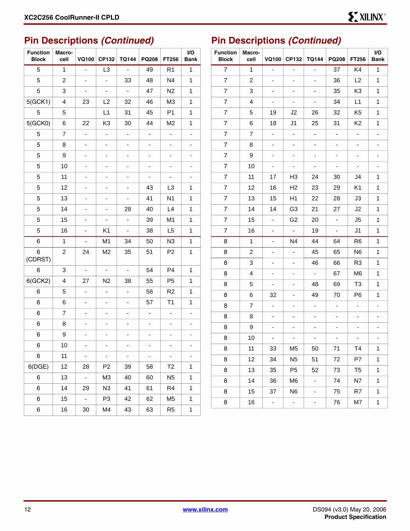
XC2C256 CoolRunner-II CPLDR
5 1 - L3 - 49 R1 1
5 2 - - 33 48 N4 1
5 3 - - - 47 N2 1
5(GCK1) 4 23 L2 32 46 M3 1
5 5 L1 31 45 P1 1
5(GCK0) 6 22 K3 30 44 M2 1
5 7 - - - - - -
5 8 - - - - - -
5 9 - - - - - -
5 10 - - - - - -
5 11 - - - - - -
5 12 - - - 43 L3 1
5 13 - - - 41 N1 1
5 14 - - 28 40 L4 1
5 15 - - - 39 M1 1
5 16 - K1 - 38 L5 1
6 1 - M1 34 50 N3 1
6 (CDRST)
2 24 M2 35 51 P2 1
6 3 - - - 54 P4 1
6(GCK2) 4 27 N2 38 55 P5 1
6 5 - - - 56 R2 1
6 6 - - - 57 T1 1
6 7 - - - - - -
6 8 - - - - - -
6 9 - - - - - -
6 10 - - - - - -
6 11 - - - - - -
6(DGE) 12 28 P2 39 58 T2 1
6 13 - M3 40 60 N5 1
6 14 29 N3 41 61 R4 1
6 15 - P3 42 62 M5 1
6 16 30 M4 43 63 R5 1
Pin Descriptions (Continued)Function
BlockMacro-
cell VQ100 CP132 TQ144 PQ208 FT256IO
Bank
7 1 - - - 37 K4 1
7 2 - - - 36 L2 1
7 3 - - - 35 K3 1
7 4 - - - 34 L1 1
7 5 19 J2 26 32 K5 1
7 6 18 J1 25 31 K2 1
7 7 - - - - - -
7 8 - - - - - -
7 9 - - - - - -
7 10 - - - - - -
7 11 17 H3 24 30 J4 1
7 12 16 H2 23 29 K1 1
7 13 15 H1 22 28 J3 1
7 14 14 G3 21 27 J2 1
7 15 - G2 20 - J5 1
7 16 - - 19 - J1 1
8 1 - N4 44 64 R6 1
8 2 - - 45 65 N6 1
8 3 - - 46 66 R3 1
8 4 - - - 67 M6 1
8 5 - - 48 69 T3 1
8 6 32 - 49 70 P6 1
8 7 - - - - - -
8 8 - - - - - -
8 9 - - - - - -
8 10 - - - - - -
8 11 33 M5 50 71 T4 1
8 12 34 N5 51 72 P7 1
8 13 35 P5 52 73 T5 1
8 14 36 M6 - 74 N7 1
8 15 37 N6 - 75 R7 1
8 16 - - - 76 M7 1
Pin Descriptions (Continued)Function
BlockMacro-
cell VQ100 CP132 TQ144 PQ208 FT256IO
Bank
12 wwwxilinxcom DS094 (v30) May 20 2006Product Specification
XC2C256 CoolRunner-II CPLDR
9 1 78 C12 112 160 B13 2
9 2 79 B12 113 161 B14 2
9 3 - - - 162 C13 2
9 4 80 A12 114 163 A15 2
9 5 164 C12 2
9 6 81 C11 115 165 B12 2
9 7 - - - - - -
9 8 - - - - - -
9 9 - - - - - -
9 10 - - - - - -
9 11 - - - 166 D13 2
9 12 82 B11 116 167 A14 2
9 13 - - 117 168 E13 2
9 14 - A11 118 169 A13 2
9 15 - - 119 170 C11 2
9 16 - C10 - 171 A12 2
10 1 77 A13 111 159 A16 2
10 2 76 B13 110 158 B15 2
10 3 74 C13 107 155 C14 2
10 4 73 C14 106 154 G11 2
10 5 72 D12 105 153 B16 2
10 6 71 D13 104 152 D15 2
10 7 - - - - - -
10 8 - - - - - -
10 9 - - - - - -
10 10 - - - - - -
10 11 151 E14 2
10 12 70 D14 103 150 C16 2
10 13 - - - 149 F14 2
10 14 - E12 102 148 F13 2
10 15 - - - 147 E15 2
10 16 - E13 101 146 G13 2
Pin Descriptions (Continued)Function
BlockMacro-
cell VQ100 CP132 TQ144 PQ208 FT256IO
Bank
11 1 - B10 - - B11 2
11 2 - - 173 D11 2
11 3 - A10 - 174 A11 2
11 4 - - - 175 D10 2
11 5 - C9 120 - B10 2
11 6 - - 121 - E12 2
11 7 - - - - - -
11 8 - - - - - -
11 9 - - - - - -
11 10 - - - - - -
11 11 85 A8 124 178 F12 2
11 12 86 B8 125 179 B9 2
11 13 87 C8 126 180 C9 2
11 14 89 - 128 182 C10 2
11 15 - - 129 183 A9 2
11 16 - - 130 184 D9 2
12 1 - - - 145 F15 2
12 2 - - 100 144 G14 2
12 3 - - - 143 E16 2
12 4 - - - 142 H12 2
12 5 - F12 - 140 F16 2
12 6 - F13 - 139 H16 2
12 7 - - - - - -
12 8 - - - - - -
12 9 - - - - - -
12 10 - - - - - -
12 11 68 F14 98 138 G15 2
12 12 - G12 97 137 H13 2
12 13 67 G13 96 136 G16 2
12 14 66 - 95 135 H14 2
12 15 65 - 94 134 H15 2
12 16 - - - - J12 2
Pin Descriptions (Continued)Function
BlockMacro-
cell VQ100 CP132 TQ144 PQ208 FT256IO
Bank
DS094 (v30) May 20 2006 wwwxilinxcom 13Product Specification
XC2C256 CoolRunner-II CPLDR
13 1 - N13 75 107 R15 1
13 2 53 N14 76 108 T16 1
13 3 - M12 77 109 N14 1
13 4 54 - - 110 R16 1
13 5 - M13 78 111 N15 1
13 6 55 - 79 112 M15 1
13 7 - - - - - -
13 8 - - - - - -
13 9 - - - - - -
13 10 - - - - - -
13 11 - - - - - -
13 12 - M14 80 113 M13 1
13 13 56 - 81 114 P16 1
13 14 - L12 82 115 N16 1
13 15 - - - 116 L14 1
13 16 - L13 - 117 M14 1
14 1 52 P14 74 106 P15 1
14 2 - - 71 103 P14 1
14 3 50 P12 70 102 P13 1
14 4 - M11 69 101 R13 1
14 5 49 N11 - 100 N13 1
14 6 - P11 68 - R14 1
14 7 - - - - - -
14 8 - - - - - -
14 9 - - - - - -
14 10 - - - - - -
14 11 - - - - - -
14 12 - - - 99 T15 1
14 13 - - 66 97 R12 1
14 14 46 P10 64 95 N11 1
14 15 44 - - - M11 1
14 16 - P9 61 91 N10 1
Pin Descriptions (Continued)Function
BlockMacro-
cell VQ100 CP132 TQ144 PQ208 FT256IO
Bank
15 1 - - - 118 L15 1
15 2 - L14 83 119 L13 1
15 3 - - - 120 M12 1
15 4 - - - 121 M16 1
15 5 - - - 122 K14 1
15 6 - - - 123 L16 1
15 7 - - - - - -
15 8 - - - - - -
15 9 - - - - - -
15 10 - - - - - -
15 11 58 K13 85 125 K15 1
15 12 59 K14 86 126 L12 1
15 13 60 J12 87 127 K16 1
15 14 61 J13 88 128 J14 1
15 15 63 H13 91 - J15 1
15 16 64 H12 92 131 J13 1
16 1 - - - 90 P10 1
16 2 - - - 89 R10 1
16 3 - M8 - 88 T10 1
16 4 - - - 87 R9 1
16 5 43 N8 60 86 N9 1
16 6 42 - 59 85 M8 1
16 7 - - - - - -
16 8 - - - - - -
16 9 - - - - - -
16 10 - - - - - -
16 11 41 P8 58 84 T8 1
16 12 40 M7 57 83 P8 1
16 13 39 N7 56 82 R8 1
16 14 - - - 80 T7 1
16 15 - - 54 78 N8 1
16 16 - P6 53 77 T6 1
Notes 1 GTS = global output enable GSR = global resetset GCK =
global clock CDRST = clock divide reset DGE = DataGATE enable
2 GTS GSR and GCK pins can be used for general purpose IO
Pin Descriptions (Continued)Function
BlockMacro-
cell VQ100 CP132 TQ144 PQ208 FT256IO
Bank
14 wwwxilinxcom DS094 (v30) May 20 2006Product Specification
XC2C256 CoolRunner-II CPLDR
XC2C256 JTAG PowerGround No Connect Pins and Total User IO
Pin Type VQ100 CP132 TQ144 PQ208 FT256
TCK 48 M10 67 98 P12
TDI 45 M9 63 94 R11
TDO 83 B9 122 176 A10
TMS 47 N10 65 96 N12
VCCAUX (JTAG supply voltage)
5 D3 8 11 F4
Power internal (VCC) 26 57 P1 K12 A2 1 37 84 1 53 124 P3 K13 D12 D5
Power Bank 1 IO (VCCIO1) 20 38 51 J3 P7 G14 P13
27 55 73 93 33 59 79 92 105 132
J6 K6 L7 L8 J11 K11 L10 L9
Power Bank 2 IO (VCCIO2) 88 98 A14 C4 A7 109 127 141 26 133 157 172 181 204
F7 F8 G6 H6 F10 F9 H11
Ground 21 25 31 62 69 75
84 100
K2 N1 P4 N9 N12 J14 H14 E14 B14
A9 B3
29 36 47 62 72 89 90 99 108 123 144
13 24 42 52 68 81 93 104 129 130 141 156 177 190
207
F11 F6 G10 G7 G8 G9 H10 H7 H8 H9 J10 J7 J8 J9 K10 K7 K8 K9 L11 L6
No connects - - - - A1 C2 E6 D1 E1 G2 F1 G1 M4 T9 P9 M9 M10 T11 T12 T13 P11 T14 J16 K12 D16 G12 C15 D14 D6 C6 E7 C5
Total user IO 80 106 118 173 184
DS094 (v30) May 20 2006 wwwxilinxcom 15Product Specification
XC2C256 CoolRunner-II CPLDR
Ordering Information
Part NumberPinBall Spacing
θJA (CWatt)
θJC (CWatt) Package Type
Package Body Dimensions IO
Commercial (C)
Industrial (I)(1)
XC2C256-6VQ100C 05mm 431 109 Very Thin Quad Flat Pack
14mm x 14mm 80 C
XC2C256-7VQ100C 05mm 431 109 Very Thin Quad Flat Pack
14mm x 14mm 80 C
XC2C256-6CP132C 05mm 650 150 Chip Scale Package 8mm x 8mm 106 C
XC2C256-7CP132C 05mm 650 150 Chip Scale Package 8mm x 8mm 106 C
XC2C256-6TQ144C 05mm 372 72 Thin Quad Flat Pack 20mm x 20mm 118 C
XC2C256-7TQ144C 05mm 372 72 Thin Quad Flat Pack 20mm x 20mm 118 C
XC2C256-6PQ208C 05mm 369 97 Plastic Quad Flat Pack
28mm x 28mm 173 C
XC2C256-7PQ208C 05mm 369 97 Plastic Quad Flat Pack
28mm x 28mm 173 C
XC2C256-6FT256C 10mm 346 61 Fine Pitch Thin BGA 17mm x 17mm 184 C
XC2C256-7FT256C 10mm 346 61 Fine Pitch Thin BGA 17mm x 17mm 184 C
XC2C256-6VQG100C 05mm 431 109 Very Thin Quad Flat Pack Pb-free
14mm x 14mm 80 C
XC2C256-7VQG100C 05mm 431 109 Very Thin Quad Flat Pack Pb-free
14mm x 14mm 80 C
XC2C256-6CPG132C 05mm 650 150 Chip Scale Package Pb-free
8mm x 8mm 106 C
XC2C256-7CPG132C 05mm 650 150 Chip Scale Package Pb-free
8mm x 8mm 106 C
XC2C256-6TQG144C 05mm 372 72 Thin Quad Flat Pack Pb-free
20mm x 20mm 118 C
XC2C256-7TQG144C 05mm 372 72 Thin Quad Flat Pack Pb-free
20mm x 20mm 118 C
XC2C256-6PQG208C 05mm 369 97 Plastic Quad Flat Pack Pb-free
28mm x 28mm 173 C
XC2C256-7PQG208C 05mm 369 97 Plastic Quad Flat Pack Pb-free
28mm x 28mm 173 C
XC2C256-6FTG256C 10mm 346 61 Fine Pitch Thin BGA Pb-free
17mm x 17mm 184 C
XC2C256-7FTG256C 10mm 346 61 Fine Pitch Thin BGA Pb-free
17mm x 17mm 184 C
XC2C256-7VQ100I 05mm 431 109 Very Thin Quad Flat Pack
14mm x 14mm 80 I
XC2C256-7CP132I 05mm 650 150 Chip Scale Package 8mm x 8mm 106 I
XC2C256-7TQ144I 05mm 372 72 Thin Quad Flat Pack 20mm x 20mm 118 I
XC2C256-7PQ208I 05mm 369 97 Plastic Quad Flat Pack
28mm x 28mm 173 I
XC2C256-7FT256I 10mm 346 61 Fine Pitch Thin BGA 17mm x 17mm 184 I
16 wwwxilinxcom DS094 (v30) May 20 2006Product Specification
XC2C256 CoolRunner-II CPLDR
Device Part Marking
Figure 5 Sample Package with Part Marking
Note Due to the small size of chip scale packages the complete ordering part number cannot be included on the packagemarking Part marking on chip scale packages by line are
bull Line 1 = X (Xilinx logo) then truncated part numberbull Line 2 = Not related to device part numberbull Line 3 = Not related to device part number
1 Line 4 = Package code speed operating temperature three digits not related to device part number Package codes C5 = CP132 C6 = CPG132
XC2C256-7VQG100I 05mm 431 109 Very Thin Quad Flat Pack Pb-free
14mm x 14mm 80 I
XC2C256-7CPG132I 05mm 650 150 Chip Scale Package Pb-free
8mm x 8mm 106 I
XC2C256-7TQG144I 05mm 372 72 Thin Quad Flat Pack Pb-free
20mm x 20mm 118 I
XC2C256-7PQG208I 05mm 369 97 Plastic Quad Flat Pack Pb-free
28mm x 28mm 173 I
XC2C256-7FTG256I 10mm 346 61 Fine Pitch Thin BGA Pb-free
17mm x 17mm 184 I
Notes 1 C = Commercial (TA = 0degC to +70degC) I = Industrial (TA = ndash40degC to +85degC)
Part NumberPinBall Spacing
θJA (CWatt)
θJC (CWatt) Package Type
Package Body Dimensions IO
Commercial (C)
Industrial (I)(1)
Standard Example XC2C128 Device Speed Grade Package Type Number of Pins Temperature Range
-6 TQ C144 Pb-Free Example XC2C128 TQ G 144 C
Device Speed Grade Package Type Pb-FreeNumber of Pins
-6
Temperature Range
XC2Cxxx
TQ144
7C
Device Type
Package
Speed
Operating Range
This line not
related to device
part number
R
Part marking for non-chip scale package
DS094 (v30) May 20 2006 wwwxilinxcom 17Product Specification
XC2C256 CoolRunner-II CPLDR
Figure 6 VQ100 Very Thin Quad Flat Pack
VQ100Top View
GN
DIO
(3)
VC
CIO
2IO IO IO IO IO IO IO IO IO V
CC
IO2
IO IO IO GN
DT
DO
IO IO IO IO IO IO IO
VC
CIO
(2)
IO(5
)
IO IOG
ND
IO IO IO IO IO IOV
CC
IO1
IO IO IO IO IO IO TD
IIO
TM
ST
CK
IO IO
GNDIOIOIOIOIOGNDIOIOIOIOIOIOGNDIOIOIOIOVCCIOIOIOIOIOVCCIO1
IO(1)IO(1)IO(1)IO(1)VAUX
IOIOIOIOIOIOIOIOIOIOIOIOIOIO
VCCIO1GND
IO(2)IO(2)IO(4)GND
12345678910111213141516171819202122232425
75747372717069686766656463626160595857565554535251
26 27 28 29 30 31 32 33 34 35 36 37 38 39 40 41 42 43 44 45 46 47 48 49 50
100 99 98 97 96 95 94 93 92 91 90 89 88 87 86 85 84 83 82 81 80 79 78 77 76
(1) - Global Output Enable(2) - Global Clock(3) - Global SetReset(4) - Clock Divide Reset(5) - Data Gate
18 wwwxilinxcom DS094 (v30) May 20 2006Product Specification
XC2C256 CoolRunner-II CPLDR
Figure 7 CP132 Chip Scale Package
CP132Bottom View
P
N
M
L
K
J
H
G
F
E
D
C
B
A
1 2 3 4 5 6 7 8 9 10 11 12 13 14
VCC VCCIO1 VCCIO1GNDIO IO IO IO IO IO IO IO IOIO(5)
IO IOVAUX IO IOIO
IO IOIO IO IOIO
IO IOIO IO VCCIO1IO
IO IOIO IO GNDIO
IO IOIO IO GNDIO
IO IOVCCIO1 IO GNDIO
IO IOIO(2) VCC IOGND
IO IOIO IO IOIO(2)
IO(1) VCCIO2 IOIOIO(3) IO IO IO GND IO IO IO VCCIO2VCC
IO IO IOIOGND IO IO IO TDO IO IO IO GNDIO(1)
IO IO IOVCCIO2IO(1) IO IO IO IO IO IO IO IOIO(1)
IO IO IOIOIO IO IO IO TDI TCK IO IO IOIO(4)
GND IO IOIOIO IO IO IO GND TMS IO GND IOIO(2)
(1) - Global Output Enable(2) - Global Clock(3) - Global SetReset(4) - Clock Divide Reset(5) - DataGATE Enable
DS094 (v30) May 20 2006 wwwxilinxcom 19Product Specification
XC2C256 CoolRunner-II CPLDR
Figure 8 TQ144 Thin Quad Flat Pack
VCCIO(1)
IO(1)
IOIO(1)
IO(1)
IOVAUX
IOIOIOIOIOIOIOIOIOIOIOIOIOIOIOIOIOIO
VCCIO1IO
GNDIO(2)
IOIO(2)
IOIO
IO(4)
GND
123456789101112131415161718192021222324252627282930313233343536
TQ144Top View
VC
CIO
(2)
IO(5
)
IO IO IO IO IO IO IOG
ND
IO IO IO IO IO IO IOV
CC
IO1
IO IO IO IO IO IOG
ND
TD
IIO
TM
SIO
TC
KIO IO IO IO
GN
D
108107106105104103102101100999897969594939291908988878685848382818079787776757473
37 38 39 40 41 42 43 44 45 46 47 48 49 50 51 52 53 54 55 56 57 58 59 60 61 62 63 64 65 66 67 68 69 70 71 72
144
143
142
141
140
139
138
137
136
135
134
133
132
131
130
129
128
127
126
125
124
123
122
121
120
119
118
117
116
115
114
113
112
111
110
109
GNDIOIOIOIOIOIOIOIOGNDIOIOIOIOIOVCCIO1IOIOGNDGNDIOIOIOIOVCCIOIOIOIOIOIOIOIOIOIOVCCIO1
GN
DIO
(3)
IO VC
CIO
2IO IO IO IO IO IO IO IO IO IO IO IO IO V
CC
IO2
IO IO IO GN
DT
DO
IO IO IO IO IO IO IO IO IO IO IO IO VC
CIO
2
(1) - Global Output Enable(2) - Global Clock(3) - Global SetReset(4) - Clock Divide Reset(5) - DataGATE Enable
20 wwwxilinxcom DS094 (v30) May 20 2006Product Specification
XC2C256 CoolRunner-II CPLDR
Figure 9 PQ208 Quad Flat Package
VCCIO
IO(1)IO
IO(1)IO
IO(1)IO
IO(1)IO
VAUXIO
GNDIOIOIOIOIOIOIOIOIOIO
GNDIO
VCCIO2IOIOIOIOIOIO
VCCIO1IOIOIOIOIOIOIOIO
GNDIO
IO(2)IO
IO(2)IOIOIOIO
IO(4)GND
PQ208Top View
VC
CI
OI
O(2
)I
OI
OI
O(5
)V
CC
IO1
IO
IO
IO
IO
IO
IO
IO
IO
GN
DI
OI
OI
OI
OI
OI
OI
OI
OI
OI
OV
CC
IO1
IO
GN
DI
OI
OI
OI
OI
OI
OI
OI
OI
OI
OV
CC
IO1
GN
DT
DI
IO
TM
SI
OT
CK
IO
IO
IO
IO
IO
GN
D
(1) - Global Output Enable(2) - Global Clock(3) - Global SetReset(4) - Clock Divide Reset(5) - DataGATE Enable
GNDIOIOIOIOIOIOIOIOIOIOIOIOIOIOGNDIOIOIOIOIOIOIOVCCIO2VCCIO1IOGNDGNDIOIOIOIOVCCIOIOIOIOIOIOIOIOIOIOIOIOIOIOIOIOIOIOVCCIO1
IO GN
DIO
(3)
IO VC
CIO
2IO IO IO IO IO IO IO IO IO IO IO IO IO G
ND
IO IO IO IO IO IO IO IO VC
CIO
2IO IO IO G
ND
TD
OIO IO IO V
CC
IO2
IO IO IO IO IO IO IO IO IO IO IO IO IO IO VC
CIO
2
12345678910111213141516171819202122232425262728293031323334353637383940414243444546474849505152
53 54 55 56 57 58 59 60 61 62 63 64 65 66 67 68 69 70 71 72 73 74 75 76 77 78 79 80 81 82 83 84 85 86 87 88 89 90 91 92 93 94 95 96 97 98 99 100
101
102
103
104
156155154153152151150149148147146145144143142141140139138137136135134133132131130129128127126125124123122121120119118117116115114113112111110109108107106105
208
207
206
205
204
203
202
201
200
199
198
197
196
195
194
193
192
191
190
189
188
187
186
185
184
183
182
181
180
179
178
177
176
175
174
173
172
171
170
169
168
167
166
165
164
163
162
161
160
159
158
157
DS094 (v30) May 20 2006 wwwxilinxcom 21Product Specification
XC2C256 CoolRunner-II CPLDR
Warranty DisclaimerTHESE PRODUCTS ARE SUBJECT TO THE TERMS OF THE XILINX LIMITED WARRANTY WHICH CAN BE VIEWEDAT httpwwwxilinxcomwarrantyhtm THIS LIMITED WARRANTY DOES NOT EXTEND TO ANY USE OF THEPRODUCTS IN AN APPLICATION OR ENVIRONMENT THAT IS NOT WITHIN THE SPECIFICATIONS STATED ON THETHEN-CURRENT XILINX DATA SHEET FOR THE PRODUCTS PRODUCTS ARE NOT DESIGNED TO BE FAIL-SAFEAND ARE NOT WARRANTED FOR USE IN APPLICATIONS THAT POSE A RISK OF PHYSICAL HARM OR LOSS OFLIFE USE OF PRODUCTS IN SUCH APPLICATIONS IS FULLY AT THE RISK OF CUSTOMER SUBJECT TOAPPLICABLE LAWS AND REGULATIONS
Figure 10 FT256 Fine Pitch Thin BGA
FT256 Bottom View
A
B
C
D
E
F
G
H
J
K
L
M
N
P
R
T
16 15 14 13 12 11 10 9 8 7 6 5 4 3 2 1
IO TDO IOIOIO IO IO IO IO IO IO IO IO IO NCIO
IO IO IOIOIO IO IO IO IO IO IO IO IO IO IOIO
IO IO IO(3)IOIO IO IO IO IO IO NC NC IO NC IONC
NC IO IO(1)IONC VCC IO IO IO IO NC VCC IO(1) IO NCIO
IO IO IOIOIO IO IO IO IO NC NC IO(1) IO(1) IO NCIO
IO VCCIO2 VAUXIOIO IO GND VCCIO2 VCCIO2 VCCIO2 GND IO IO IO NCIO
IO GND IOIOIO NC IO GND GND GND VCCIO2 IO IO NC NCIO
IO GND IOIOIO IO VCCIO2 GND GND GND VCCIO2 IO IO IO IOIO
NC GND IOIOIO IO VCCIO1 GND GND GND VCCIO1 IO IO IO IOIO
IO GND IOVCCIO NC VCCIO1 GND GND GND VCCIO1 IO IO IO IOIO
IO VCCIO1 IOIOIO IO GND VCCIO1 VCCIO1 VCCIO1 GND IO IO IO IOIO
IO NC NCIOIO IO IO NC IO IO IO IO IO(2) IO(2) IOIO
IO IO IOIOIO TMS IO IO IO IO IO IO IO IO IOIO
IO IO IOIOIO TCK NC NC IO IO IO IO(2) VCC IO(4) IOIO
IO IO IOIOIO IO TDI IO IO IO IO IO IO IO IOIO
IO IO IONCNC NC NC NC IO IO IO IO IO IO(5) IOIO
(1) - Global Output Enable(2) - Global Clock(3) - Global SetReset(4) - Clock Divide Reset(5) - DataGATE Enable
22 wwwxilinxcom DS094 (v30) May 20 2006Product Specification
XC2C256 CoolRunner-II CPLDR
Additional InformationAdditional information is available for the following CoolRunner-II topics
bull XAPP784 Bulletproof CPLD Design Practicesbull XAPP375 Timing Model bull XAPP376 Logic Engine bull XAPP378 Advanced Features bull XAPP382 IO Characteristics bull XAPP389 Powering CoolRunner-II bull XAPP399 Assigning VREF Pins
To access these and all application notes with their associ-ated reference designs click the following link and scrolldown the page until you find the document you want
CoolRunner-II Data Sheets and Application Notes
Device Packages
Revision HistoryThe following table shows the revision history for this document
Date Version Revision
050902 10 Initial Xilinx release
051302 11 Updated AC Electrical Characteristics and added new parameters
103102 12 Corrected package user IO added Voltage Referenced DC tables
031703 20 Added Characterization numbers for product release and device part marking
040203 21 Updated TSOL max from 260 to 220 Changed ICCSB units from mA to μA
012604 22 Updated Device Part Marking Updated links and Tsol
022604 23 Corrected Theta JC value on XC2C256-7TQ144
080304 24 Pb-free documentation
081904 25 Changes to ICCSB maximum specifications in DC Electrical Characteristics table on page 3
100104 26 Add Asynchronous PresetReset Pulse Width specification to AC Electrical Characteristics
030705 27 Removed -5 speed grade Changes to Table 1 IO Standards
062805 28 Move to Product Specification Change to TIN25 TOUT25 TIN33 and TOUT33 for -7 speed grade
032006 29 Add Warranty Disclaimer Add note to Pin Description table that GTS GSR and GCK pins can be used for general purpose IO
52006 30 Moved TCONFIG specification values from MIN column to MAX column page 7
DS094 (v30) May 20 2006 wwwxilinxcom 23Product Specification
- Features
- Description
- RealDigital Design Technology
- Supported IO Standards
- Absolute Maximum Ratings
- Recommended Operating Conditions
- DC Electrical Characteristics (Over Recommended Operating Conditions)
- LVCMOS 33V and LVTTL 33V DC Voltage Specifications
- LVCMOS 25V DC Voltage Specifications
- LVCMOS 18V DC Voltage Specifications
- LVCMOS 15V DC Voltage Specifications(1)
- Schmitt Trigger Input DC Voltage Specifications
- SSTL2-1 DC Voltage Specifications
- SSTL3-1 DC Voltage Specifications
- HSTL1 DC Voltage Specifications
- AC Electrical Characteristics Over Recommended Operating Conditions
- Internal Timing Parameters
-
- Switching Characteristics
- AC Test Circuit
-
- Pin Descriptions
-
- XC2C256 JTAG PowerGround No Connect Pins and Total User IO
-
- Warranty Disclaimer
- Additional Information
- Revision History
-
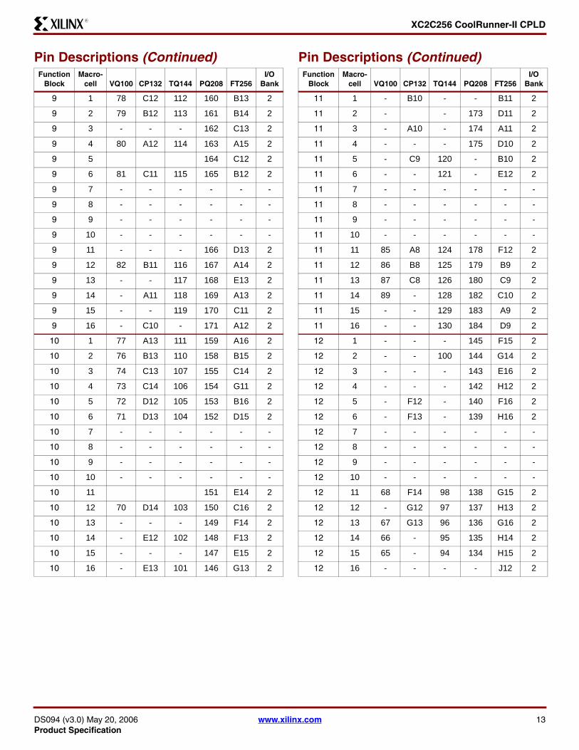
XC2C256 CoolRunner-II CPLDR
9 1 78 C12 112 160 B13 2
9 2 79 B12 113 161 B14 2
9 3 - - - 162 C13 2
9 4 80 A12 114 163 A15 2
9 5 164 C12 2
9 6 81 C11 115 165 B12 2
9 7 - - - - - -
9 8 - - - - - -
9 9 - - - - - -
9 10 - - - - - -
9 11 - - - 166 D13 2
9 12 82 B11 116 167 A14 2
9 13 - - 117 168 E13 2
9 14 - A11 118 169 A13 2
9 15 - - 119 170 C11 2
9 16 - C10 - 171 A12 2
10 1 77 A13 111 159 A16 2
10 2 76 B13 110 158 B15 2
10 3 74 C13 107 155 C14 2
10 4 73 C14 106 154 G11 2
10 5 72 D12 105 153 B16 2
10 6 71 D13 104 152 D15 2
10 7 - - - - - -
10 8 - - - - - -
10 9 - - - - - -
10 10 - - - - - -
10 11 151 E14 2
10 12 70 D14 103 150 C16 2
10 13 - - - 149 F14 2
10 14 - E12 102 148 F13 2
10 15 - - - 147 E15 2
10 16 - E13 101 146 G13 2
Pin Descriptions (Continued)Function
BlockMacro-
cell VQ100 CP132 TQ144 PQ208 FT256IO
Bank
11 1 - B10 - - B11 2
11 2 - - 173 D11 2
11 3 - A10 - 174 A11 2
11 4 - - - 175 D10 2
11 5 - C9 120 - B10 2
11 6 - - 121 - E12 2
11 7 - - - - - -
11 8 - - - - - -
11 9 - - - - - -
11 10 - - - - - -
11 11 85 A8 124 178 F12 2
11 12 86 B8 125 179 B9 2
11 13 87 C8 126 180 C9 2
11 14 89 - 128 182 C10 2
11 15 - - 129 183 A9 2
11 16 - - 130 184 D9 2
12 1 - - - 145 F15 2
12 2 - - 100 144 G14 2
12 3 - - - 143 E16 2
12 4 - - - 142 H12 2
12 5 - F12 - 140 F16 2
12 6 - F13 - 139 H16 2
12 7 - - - - - -
12 8 - - - - - -
12 9 - - - - - -
12 10 - - - - - -
12 11 68 F14 98 138 G15 2
12 12 - G12 97 137 H13 2
12 13 67 G13 96 136 G16 2
12 14 66 - 95 135 H14 2
12 15 65 - 94 134 H15 2
12 16 - - - - J12 2
Pin Descriptions (Continued)Function
BlockMacro-
cell VQ100 CP132 TQ144 PQ208 FT256IO
Bank
DS094 (v30) May 20 2006 wwwxilinxcom 13Product Specification
XC2C256 CoolRunner-II CPLDR
13 1 - N13 75 107 R15 1
13 2 53 N14 76 108 T16 1
13 3 - M12 77 109 N14 1
13 4 54 - - 110 R16 1
13 5 - M13 78 111 N15 1
13 6 55 - 79 112 M15 1
13 7 - - - - - -
13 8 - - - - - -
13 9 - - - - - -
13 10 - - - - - -
13 11 - - - - - -
13 12 - M14 80 113 M13 1
13 13 56 - 81 114 P16 1
13 14 - L12 82 115 N16 1
13 15 - - - 116 L14 1
13 16 - L13 - 117 M14 1
14 1 52 P14 74 106 P15 1
14 2 - - 71 103 P14 1
14 3 50 P12 70 102 P13 1
14 4 - M11 69 101 R13 1
14 5 49 N11 - 100 N13 1
14 6 - P11 68 - R14 1
14 7 - - - - - -
14 8 - - - - - -
14 9 - - - - - -
14 10 - - - - - -
14 11 - - - - - -
14 12 - - - 99 T15 1
14 13 - - 66 97 R12 1
14 14 46 P10 64 95 N11 1
14 15 44 - - - M11 1
14 16 - P9 61 91 N10 1
Pin Descriptions (Continued)Function
BlockMacro-
cell VQ100 CP132 TQ144 PQ208 FT256IO
Bank
15 1 - - - 118 L15 1
15 2 - L14 83 119 L13 1
15 3 - - - 120 M12 1
15 4 - - - 121 M16 1
15 5 - - - 122 K14 1
15 6 - - - 123 L16 1
15 7 - - - - - -
15 8 - - - - - -
15 9 - - - - - -
15 10 - - - - - -
15 11 58 K13 85 125 K15 1
15 12 59 K14 86 126 L12 1
15 13 60 J12 87 127 K16 1
15 14 61 J13 88 128 J14 1
15 15 63 H13 91 - J15 1
15 16 64 H12 92 131 J13 1
16 1 - - - 90 P10 1
16 2 - - - 89 R10 1
16 3 - M8 - 88 T10 1
16 4 - - - 87 R9 1
16 5 43 N8 60 86 N9 1
16 6 42 - 59 85 M8 1
16 7 - - - - - -
16 8 - - - - - -
16 9 - - - - - -
16 10 - - - - - -
16 11 41 P8 58 84 T8 1
16 12 40 M7 57 83 P8 1
16 13 39 N7 56 82 R8 1
16 14 - - - 80 T7 1
16 15 - - 54 78 N8 1
16 16 - P6 53 77 T6 1
Notes 1 GTS = global output enable GSR = global resetset GCK =
global clock CDRST = clock divide reset DGE = DataGATE enable
2 GTS GSR and GCK pins can be used for general purpose IO
Pin Descriptions (Continued)Function
BlockMacro-
cell VQ100 CP132 TQ144 PQ208 FT256IO
Bank
14 wwwxilinxcom DS094 (v30) May 20 2006Product Specification
XC2C256 CoolRunner-II CPLDR
XC2C256 JTAG PowerGround No Connect Pins and Total User IO
Pin Type VQ100 CP132 TQ144 PQ208 FT256
TCK 48 M10 67 98 P12
TDI 45 M9 63 94 R11
TDO 83 B9 122 176 A10
TMS 47 N10 65 96 N12
VCCAUX (JTAG supply voltage)
5 D3 8 11 F4
Power internal (VCC) 26 57 P1 K12 A2 1 37 84 1 53 124 P3 K13 D12 D5
Power Bank 1 IO (VCCIO1) 20 38 51 J3 P7 G14 P13
27 55 73 93 33 59 79 92 105 132
J6 K6 L7 L8 J11 K11 L10 L9
Power Bank 2 IO (VCCIO2) 88 98 A14 C4 A7 109 127 141 26 133 157 172 181 204
F7 F8 G6 H6 F10 F9 H11
Ground 21 25 31 62 69 75
84 100
K2 N1 P4 N9 N12 J14 H14 E14 B14
A9 B3
29 36 47 62 72 89 90 99 108 123 144
13 24 42 52 68 81 93 104 129 130 141 156 177 190
207
F11 F6 G10 G7 G8 G9 H10 H7 H8 H9 J10 J7 J8 J9 K10 K7 K8 K9 L11 L6
No connects - - - - A1 C2 E6 D1 E1 G2 F1 G1 M4 T9 P9 M9 M10 T11 T12 T13 P11 T14 J16 K12 D16 G12 C15 D14 D6 C6 E7 C5
Total user IO 80 106 118 173 184
DS094 (v30) May 20 2006 wwwxilinxcom 15Product Specification
XC2C256 CoolRunner-II CPLDR
Ordering Information
Part NumberPinBall Spacing
θJA (CWatt)
θJC (CWatt) Package Type
Package Body Dimensions IO
Commercial (C)
Industrial (I)(1)
XC2C256-6VQ100C 05mm 431 109 Very Thin Quad Flat Pack
14mm x 14mm 80 C
XC2C256-7VQ100C 05mm 431 109 Very Thin Quad Flat Pack
14mm x 14mm 80 C
XC2C256-6CP132C 05mm 650 150 Chip Scale Package 8mm x 8mm 106 C
XC2C256-7CP132C 05mm 650 150 Chip Scale Package 8mm x 8mm 106 C
XC2C256-6TQ144C 05mm 372 72 Thin Quad Flat Pack 20mm x 20mm 118 C
XC2C256-7TQ144C 05mm 372 72 Thin Quad Flat Pack 20mm x 20mm 118 C
XC2C256-6PQ208C 05mm 369 97 Plastic Quad Flat Pack
28mm x 28mm 173 C
XC2C256-7PQ208C 05mm 369 97 Plastic Quad Flat Pack
28mm x 28mm 173 C
XC2C256-6FT256C 10mm 346 61 Fine Pitch Thin BGA 17mm x 17mm 184 C
XC2C256-7FT256C 10mm 346 61 Fine Pitch Thin BGA 17mm x 17mm 184 C
XC2C256-6VQG100C 05mm 431 109 Very Thin Quad Flat Pack Pb-free
14mm x 14mm 80 C
XC2C256-7VQG100C 05mm 431 109 Very Thin Quad Flat Pack Pb-free
14mm x 14mm 80 C
XC2C256-6CPG132C 05mm 650 150 Chip Scale Package Pb-free
8mm x 8mm 106 C
XC2C256-7CPG132C 05mm 650 150 Chip Scale Package Pb-free
8mm x 8mm 106 C
XC2C256-6TQG144C 05mm 372 72 Thin Quad Flat Pack Pb-free
20mm x 20mm 118 C
XC2C256-7TQG144C 05mm 372 72 Thin Quad Flat Pack Pb-free
20mm x 20mm 118 C
XC2C256-6PQG208C 05mm 369 97 Plastic Quad Flat Pack Pb-free
28mm x 28mm 173 C
XC2C256-7PQG208C 05mm 369 97 Plastic Quad Flat Pack Pb-free
28mm x 28mm 173 C
XC2C256-6FTG256C 10mm 346 61 Fine Pitch Thin BGA Pb-free
17mm x 17mm 184 C
XC2C256-7FTG256C 10mm 346 61 Fine Pitch Thin BGA Pb-free
17mm x 17mm 184 C
XC2C256-7VQ100I 05mm 431 109 Very Thin Quad Flat Pack
14mm x 14mm 80 I
XC2C256-7CP132I 05mm 650 150 Chip Scale Package 8mm x 8mm 106 I
XC2C256-7TQ144I 05mm 372 72 Thin Quad Flat Pack 20mm x 20mm 118 I
XC2C256-7PQ208I 05mm 369 97 Plastic Quad Flat Pack
28mm x 28mm 173 I
XC2C256-7FT256I 10mm 346 61 Fine Pitch Thin BGA 17mm x 17mm 184 I
16 wwwxilinxcom DS094 (v30) May 20 2006Product Specification
XC2C256 CoolRunner-II CPLDR
Device Part Marking
Figure 5 Sample Package with Part Marking
Note Due to the small size of chip scale packages the complete ordering part number cannot be included on the packagemarking Part marking on chip scale packages by line are
bull Line 1 = X (Xilinx logo) then truncated part numberbull Line 2 = Not related to device part numberbull Line 3 = Not related to device part number
1 Line 4 = Package code speed operating temperature three digits not related to device part number Package codes C5 = CP132 C6 = CPG132
XC2C256-7VQG100I 05mm 431 109 Very Thin Quad Flat Pack Pb-free
14mm x 14mm 80 I
XC2C256-7CPG132I 05mm 650 150 Chip Scale Package Pb-free
8mm x 8mm 106 I
XC2C256-7TQG144I 05mm 372 72 Thin Quad Flat Pack Pb-free
20mm x 20mm 118 I
XC2C256-7PQG208I 05mm 369 97 Plastic Quad Flat Pack Pb-free
28mm x 28mm 173 I
XC2C256-7FTG256I 10mm 346 61 Fine Pitch Thin BGA Pb-free
17mm x 17mm 184 I
Notes 1 C = Commercial (TA = 0degC to +70degC) I = Industrial (TA = ndash40degC to +85degC)
Part NumberPinBall Spacing
θJA (CWatt)
θJC (CWatt) Package Type
Package Body Dimensions IO
Commercial (C)
Industrial (I)(1)
Standard Example XC2C128 Device Speed Grade Package Type Number of Pins Temperature Range
-6 TQ C144 Pb-Free Example XC2C128 TQ G 144 C
Device Speed Grade Package Type Pb-FreeNumber of Pins
-6
Temperature Range
XC2Cxxx
TQ144
7C
Device Type
Package
Speed
Operating Range
This line not
related to device
part number
R
Part marking for non-chip scale package
DS094 (v30) May 20 2006 wwwxilinxcom 17Product Specification
XC2C256 CoolRunner-II CPLDR
Figure 6 VQ100 Very Thin Quad Flat Pack
VQ100Top View
GN
DIO
(3)
VC
CIO
2IO IO IO IO IO IO IO IO IO V
CC
IO2
IO IO IO GN
DT
DO
IO IO IO IO IO IO IO
VC
CIO
(2)
IO(5
)
IO IOG
ND
IO IO IO IO IO IOV
CC
IO1
IO IO IO IO IO IO TD
IIO
TM
ST
CK
IO IO
GNDIOIOIOIOIOGNDIOIOIOIOIOIOGNDIOIOIOIOVCCIOIOIOIOIOVCCIO1
IO(1)IO(1)IO(1)IO(1)VAUX
IOIOIOIOIOIOIOIOIOIOIOIOIOIO
VCCIO1GND
IO(2)IO(2)IO(4)GND
12345678910111213141516171819202122232425
75747372717069686766656463626160595857565554535251
26 27 28 29 30 31 32 33 34 35 36 37 38 39 40 41 42 43 44 45 46 47 48 49 50
100 99 98 97 96 95 94 93 92 91 90 89 88 87 86 85 84 83 82 81 80 79 78 77 76
(1) - Global Output Enable(2) - Global Clock(3) - Global SetReset(4) - Clock Divide Reset(5) - Data Gate
18 wwwxilinxcom DS094 (v30) May 20 2006Product Specification
XC2C256 CoolRunner-II CPLDR
Figure 7 CP132 Chip Scale Package
CP132Bottom View
P
N
M
L
K
J
H
G
F
E
D
C
B
A
1 2 3 4 5 6 7 8 9 10 11 12 13 14
VCC VCCIO1 VCCIO1GNDIO IO IO IO IO IO IO IO IOIO(5)
IO IOVAUX IO IOIO
IO IOIO IO IOIO
IO IOIO IO VCCIO1IO
IO IOIO IO GNDIO
IO IOIO IO GNDIO
IO IOVCCIO1 IO GNDIO
IO IOIO(2) VCC IOGND
IO IOIO IO IOIO(2)
IO(1) VCCIO2 IOIOIO(3) IO IO IO GND IO IO IO VCCIO2VCC
IO IO IOIOGND IO IO IO TDO IO IO IO GNDIO(1)
IO IO IOVCCIO2IO(1) IO IO IO IO IO IO IO IOIO(1)
IO IO IOIOIO IO IO IO TDI TCK IO IO IOIO(4)
GND IO IOIOIO IO IO IO GND TMS IO GND IOIO(2)
(1) - Global Output Enable(2) - Global Clock(3) - Global SetReset(4) - Clock Divide Reset(5) - DataGATE Enable
DS094 (v30) May 20 2006 wwwxilinxcom 19Product Specification
XC2C256 CoolRunner-II CPLDR
Figure 8 TQ144 Thin Quad Flat Pack
VCCIO(1)
IO(1)
IOIO(1)
IO(1)
IOVAUX
IOIOIOIOIOIOIOIOIOIOIOIOIOIOIOIOIOIO
VCCIO1IO
GNDIO(2)
IOIO(2)
IOIO
IO(4)
GND
123456789101112131415161718192021222324252627282930313233343536
TQ144Top View
VC
CIO
(2)
IO(5
)
IO IO IO IO IO IO IOG
ND
IO IO IO IO IO IO IOV
CC
IO1
IO IO IO IO IO IOG
ND
TD
IIO
TM
SIO
TC
KIO IO IO IO
GN
D
108107106105104103102101100999897969594939291908988878685848382818079787776757473
37 38 39 40 41 42 43 44 45 46 47 48 49 50 51 52 53 54 55 56 57 58 59 60 61 62 63 64 65 66 67 68 69 70 71 72
144
143
142
141
140
139
138
137
136
135
134
133
132
131
130
129
128
127
126
125
124
123
122
121
120
119
118
117
116
115
114
113
112
111
110
109
GNDIOIOIOIOIOIOIOIOGNDIOIOIOIOIOVCCIO1IOIOGNDGNDIOIOIOIOVCCIOIOIOIOIOIOIOIOIOIOVCCIO1
GN
DIO
(3)
IO VC
CIO
2IO IO IO IO IO IO IO IO IO IO IO IO IO V
CC
IO2
IO IO IO GN
DT
DO
IO IO IO IO IO IO IO IO IO IO IO IO VC
CIO
2
(1) - Global Output Enable(2) - Global Clock(3) - Global SetReset(4) - Clock Divide Reset(5) - DataGATE Enable
20 wwwxilinxcom DS094 (v30) May 20 2006Product Specification
XC2C256 CoolRunner-II CPLDR
Figure 9 PQ208 Quad Flat Package
VCCIO
IO(1)IO
IO(1)IO
IO(1)IO
IO(1)IO
VAUXIO
GNDIOIOIOIOIOIOIOIOIOIO
GNDIO
VCCIO2IOIOIOIOIOIO
VCCIO1IOIOIOIOIOIOIOIO
GNDIO
IO(2)IO
IO(2)IOIOIOIO
IO(4)GND
PQ208Top View
VC
CI
OI
O(2
)I
OI
OI
O(5
)V
CC
IO1
IO
IO
IO
IO
IO
IO
IO
IO
GN
DI
OI
OI
OI
OI
OI
OI
OI
OI
OI
OV
CC
IO1
IO
GN
DI
OI
OI
OI
OI
OI
OI
OI
OI
OI
OV
CC
IO1
GN
DT
DI
IO
TM
SI
OT
CK
IO
IO
IO
IO
IO
GN
D
(1) - Global Output Enable(2) - Global Clock(3) - Global SetReset(4) - Clock Divide Reset(5) - DataGATE Enable
GNDIOIOIOIOIOIOIOIOIOIOIOIOIOIOGNDIOIOIOIOIOIOIOVCCIO2VCCIO1IOGNDGNDIOIOIOIOVCCIOIOIOIOIOIOIOIOIOIOIOIOIOIOIOIOIOIOVCCIO1
IO GN
DIO
(3)
IO VC
CIO
2IO IO IO IO IO IO IO IO IO IO IO IO IO G
ND
IO IO IO IO IO IO IO IO VC
CIO
2IO IO IO G
ND
TD
OIO IO IO V
CC
IO2
IO IO IO IO IO IO IO IO IO IO IO IO IO IO VC
CIO
2
12345678910111213141516171819202122232425262728293031323334353637383940414243444546474849505152
53 54 55 56 57 58 59 60 61 62 63 64 65 66 67 68 69 70 71 72 73 74 75 76 77 78 79 80 81 82 83 84 85 86 87 88 89 90 91 92 93 94 95 96 97 98 99 100
101
102
103
104
156155154153152151150149148147146145144143142141140139138137136135134133132131130129128127126125124123122121120119118117116115114113112111110109108107106105
208
207
206
205
204
203
202
201
200
199
198
197
196
195
194
193
192
191
190
189
188
187
186
185
184
183
182
181
180
179
178
177
176
175
174
173
172
171
170
169
168
167
166
165
164
163
162
161
160
159
158
157
DS094 (v30) May 20 2006 wwwxilinxcom 21Product Specification
XC2C256 CoolRunner-II CPLDR
Warranty DisclaimerTHESE PRODUCTS ARE SUBJECT TO THE TERMS OF THE XILINX LIMITED WARRANTY WHICH CAN BE VIEWEDAT httpwwwxilinxcomwarrantyhtm THIS LIMITED WARRANTY DOES NOT EXTEND TO ANY USE OF THEPRODUCTS IN AN APPLICATION OR ENVIRONMENT THAT IS NOT WITHIN THE SPECIFICATIONS STATED ON THETHEN-CURRENT XILINX DATA SHEET FOR THE PRODUCTS PRODUCTS ARE NOT DESIGNED TO BE FAIL-SAFEAND ARE NOT WARRANTED FOR USE IN APPLICATIONS THAT POSE A RISK OF PHYSICAL HARM OR LOSS OFLIFE USE OF PRODUCTS IN SUCH APPLICATIONS IS FULLY AT THE RISK OF CUSTOMER SUBJECT TOAPPLICABLE LAWS AND REGULATIONS
Figure 10 FT256 Fine Pitch Thin BGA
FT256 Bottom View
A
B
C
D
E
F
G
H
J
K
L
M
N
P
R
T
16 15 14 13 12 11 10 9 8 7 6 5 4 3 2 1
IO TDO IOIOIO IO IO IO IO IO IO IO IO IO NCIO
IO IO IOIOIO IO IO IO IO IO IO IO IO IO IOIO
IO IO IO(3)IOIO IO IO IO IO IO NC NC IO NC IONC
NC IO IO(1)IONC VCC IO IO IO IO NC VCC IO(1) IO NCIO
IO IO IOIOIO IO IO IO IO NC NC IO(1) IO(1) IO NCIO
IO VCCIO2 VAUXIOIO IO GND VCCIO2 VCCIO2 VCCIO2 GND IO IO IO NCIO
IO GND IOIOIO NC IO GND GND GND VCCIO2 IO IO NC NCIO
IO GND IOIOIO IO VCCIO2 GND GND GND VCCIO2 IO IO IO IOIO
NC GND IOIOIO IO VCCIO1 GND GND GND VCCIO1 IO IO IO IOIO
IO GND IOVCCIO NC VCCIO1 GND GND GND VCCIO1 IO IO IO IOIO
IO VCCIO1 IOIOIO IO GND VCCIO1 VCCIO1 VCCIO1 GND IO IO IO IOIO
IO NC NCIOIO IO IO NC IO IO IO IO IO(2) IO(2) IOIO
IO IO IOIOIO TMS IO IO IO IO IO IO IO IO IOIO
IO IO IOIOIO TCK NC NC IO IO IO IO(2) VCC IO(4) IOIO
IO IO IOIOIO IO TDI IO IO IO IO IO IO IO IOIO
IO IO IONCNC NC NC NC IO IO IO IO IO IO(5) IOIO
(1) - Global Output Enable(2) - Global Clock(3) - Global SetReset(4) - Clock Divide Reset(5) - DataGATE Enable
22 wwwxilinxcom DS094 (v30) May 20 2006Product Specification
XC2C256 CoolRunner-II CPLDR
Additional InformationAdditional information is available for the following CoolRunner-II topics
bull XAPP784 Bulletproof CPLD Design Practicesbull XAPP375 Timing Model bull XAPP376 Logic Engine bull XAPP378 Advanced Features bull XAPP382 IO Characteristics bull XAPP389 Powering CoolRunner-II bull XAPP399 Assigning VREF Pins
To access these and all application notes with their associ-ated reference designs click the following link and scrolldown the page until you find the document you want
CoolRunner-II Data Sheets and Application Notes
Device Packages
Revision HistoryThe following table shows the revision history for this document
Date Version Revision
050902 10 Initial Xilinx release
051302 11 Updated AC Electrical Characteristics and added new parameters
103102 12 Corrected package user IO added Voltage Referenced DC tables
031703 20 Added Characterization numbers for product release and device part marking
040203 21 Updated TSOL max from 260 to 220 Changed ICCSB units from mA to μA
012604 22 Updated Device Part Marking Updated links and Tsol
022604 23 Corrected Theta JC value on XC2C256-7TQ144
080304 24 Pb-free documentation
081904 25 Changes to ICCSB maximum specifications in DC Electrical Characteristics table on page 3
100104 26 Add Asynchronous PresetReset Pulse Width specification to AC Electrical Characteristics
030705 27 Removed -5 speed grade Changes to Table 1 IO Standards
062805 28 Move to Product Specification Change to TIN25 TOUT25 TIN33 and TOUT33 for -7 speed grade
032006 29 Add Warranty Disclaimer Add note to Pin Description table that GTS GSR and GCK pins can be used for general purpose IO
52006 30 Moved TCONFIG specification values from MIN column to MAX column page 7
DS094 (v30) May 20 2006 wwwxilinxcom 23Product Specification
- Features
- Description
- RealDigital Design Technology
- Supported IO Standards
- Absolute Maximum Ratings
- Recommended Operating Conditions
- DC Electrical Characteristics (Over Recommended Operating Conditions)
- LVCMOS 33V and LVTTL 33V DC Voltage Specifications
- LVCMOS 25V DC Voltage Specifications
- LVCMOS 18V DC Voltage Specifications
- LVCMOS 15V DC Voltage Specifications(1)
- Schmitt Trigger Input DC Voltage Specifications
- SSTL2-1 DC Voltage Specifications
- SSTL3-1 DC Voltage Specifications
- HSTL1 DC Voltage Specifications
- AC Electrical Characteristics Over Recommended Operating Conditions
- Internal Timing Parameters
-
- Switching Characteristics
- AC Test Circuit
-
- Pin Descriptions
-
- XC2C256 JTAG PowerGround No Connect Pins and Total User IO
-
- Warranty Disclaimer
- Additional Information
- Revision History
-
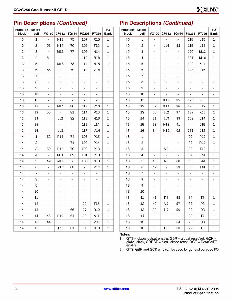
XC2C256 CoolRunner-II CPLDR
13 1 - N13 75 107 R15 1
13 2 53 N14 76 108 T16 1
13 3 - M12 77 109 N14 1
13 4 54 - - 110 R16 1
13 5 - M13 78 111 N15 1
13 6 55 - 79 112 M15 1
13 7 - - - - - -
13 8 - - - - - -
13 9 - - - - - -
13 10 - - - - - -
13 11 - - - - - -
13 12 - M14 80 113 M13 1
13 13 56 - 81 114 P16 1
13 14 - L12 82 115 N16 1
13 15 - - - 116 L14 1
13 16 - L13 - 117 M14 1
14 1 52 P14 74 106 P15 1
14 2 - - 71 103 P14 1
14 3 50 P12 70 102 P13 1
14 4 - M11 69 101 R13 1
14 5 49 N11 - 100 N13 1
14 6 - P11 68 - R14 1
14 7 - - - - - -
14 8 - - - - - -
14 9 - - - - - -
14 10 - - - - - -
14 11 - - - - - -
14 12 - - - 99 T15 1
14 13 - - 66 97 R12 1
14 14 46 P10 64 95 N11 1
14 15 44 - - - M11 1
14 16 - P9 61 91 N10 1
Pin Descriptions (Continued)Function
BlockMacro-
cell VQ100 CP132 TQ144 PQ208 FT256IO
Bank
15 1 - - - 118 L15 1
15 2 - L14 83 119 L13 1
15 3 - - - 120 M12 1
15 4 - - - 121 M16 1
15 5 - - - 122 K14 1
15 6 - - - 123 L16 1
15 7 - - - - - -
15 8 - - - - - -
15 9 - - - - - -
15 10 - - - - - -
15 11 58 K13 85 125 K15 1
15 12 59 K14 86 126 L12 1
15 13 60 J12 87 127 K16 1
15 14 61 J13 88 128 J14 1
15 15 63 H13 91 - J15 1
15 16 64 H12 92 131 J13 1
16 1 - - - 90 P10 1
16 2 - - - 89 R10 1
16 3 - M8 - 88 T10 1
16 4 - - - 87 R9 1
16 5 43 N8 60 86 N9 1
16 6 42 - 59 85 M8 1
16 7 - - - - - -
16 8 - - - - - -
16 9 - - - - - -
16 10 - - - - - -
16 11 41 P8 58 84 T8 1
16 12 40 M7 57 83 P8 1
16 13 39 N7 56 82 R8 1
16 14 - - - 80 T7 1
16 15 - - 54 78 N8 1
16 16 - P6 53 77 T6 1
Notes 1 GTS = global output enable GSR = global resetset GCK =
global clock CDRST = clock divide reset DGE = DataGATE enable
2 GTS GSR and GCK pins can be used for general purpose IO
Pin Descriptions (Continued)Function
BlockMacro-
cell VQ100 CP132 TQ144 PQ208 FT256IO
Bank
14 wwwxilinxcom DS094 (v30) May 20 2006Product Specification
XC2C256 CoolRunner-II CPLDR
XC2C256 JTAG PowerGround No Connect Pins and Total User IO
Pin Type VQ100 CP132 TQ144 PQ208 FT256
TCK 48 M10 67 98 P12
TDI 45 M9 63 94 R11
TDO 83 B9 122 176 A10
TMS 47 N10 65 96 N12
VCCAUX (JTAG supply voltage)
5 D3 8 11 F4
Power internal (VCC) 26 57 P1 K12 A2 1 37 84 1 53 124 P3 K13 D12 D5
Power Bank 1 IO (VCCIO1) 20 38 51 J3 P7 G14 P13
27 55 73 93 33 59 79 92 105 132
J6 K6 L7 L8 J11 K11 L10 L9
Power Bank 2 IO (VCCIO2) 88 98 A14 C4 A7 109 127 141 26 133 157 172 181 204
F7 F8 G6 H6 F10 F9 H11
Ground 21 25 31 62 69 75
84 100
K2 N1 P4 N9 N12 J14 H14 E14 B14
A9 B3
29 36 47 62 72 89 90 99 108 123 144
13 24 42 52 68 81 93 104 129 130 141 156 177 190
207
F11 F6 G10 G7 G8 G9 H10 H7 H8 H9 J10 J7 J8 J9 K10 K7 K8 K9 L11 L6
No connects - - - - A1 C2 E6 D1 E1 G2 F1 G1 M4 T9 P9 M9 M10 T11 T12 T13 P11 T14 J16 K12 D16 G12 C15 D14 D6 C6 E7 C5
Total user IO 80 106 118 173 184
DS094 (v30) May 20 2006 wwwxilinxcom 15Product Specification
XC2C256 CoolRunner-II CPLDR
Ordering Information
Part NumberPinBall Spacing
θJA (CWatt)
θJC (CWatt) Package Type
Package Body Dimensions IO
Commercial (C)
Industrial (I)(1)
XC2C256-6VQ100C 05mm 431 109 Very Thin Quad Flat Pack
14mm x 14mm 80 C
XC2C256-7VQ100C 05mm 431 109 Very Thin Quad Flat Pack
14mm x 14mm 80 C
XC2C256-6CP132C 05mm 650 150 Chip Scale Package 8mm x 8mm 106 C
XC2C256-7CP132C 05mm 650 150 Chip Scale Package 8mm x 8mm 106 C
XC2C256-6TQ144C 05mm 372 72 Thin Quad Flat Pack 20mm x 20mm 118 C
XC2C256-7TQ144C 05mm 372 72 Thin Quad Flat Pack 20mm x 20mm 118 C
XC2C256-6PQ208C 05mm 369 97 Plastic Quad Flat Pack
28mm x 28mm 173 C
XC2C256-7PQ208C 05mm 369 97 Plastic Quad Flat Pack
28mm x 28mm 173 C
XC2C256-6FT256C 10mm 346 61 Fine Pitch Thin BGA 17mm x 17mm 184 C
XC2C256-7FT256C 10mm 346 61 Fine Pitch Thin BGA 17mm x 17mm 184 C
XC2C256-6VQG100C 05mm 431 109 Very Thin Quad Flat Pack Pb-free
14mm x 14mm 80 C
XC2C256-7VQG100C 05mm 431 109 Very Thin Quad Flat Pack Pb-free
14mm x 14mm 80 C
XC2C256-6CPG132C 05mm 650 150 Chip Scale Package Pb-free
8mm x 8mm 106 C
XC2C256-7CPG132C 05mm 650 150 Chip Scale Package Pb-free
8mm x 8mm 106 C
XC2C256-6TQG144C 05mm 372 72 Thin Quad Flat Pack Pb-free
20mm x 20mm 118 C
XC2C256-7TQG144C 05mm 372 72 Thin Quad Flat Pack Pb-free
20mm x 20mm 118 C
XC2C256-6PQG208C 05mm 369 97 Plastic Quad Flat Pack Pb-free
28mm x 28mm 173 C
XC2C256-7PQG208C 05mm 369 97 Plastic Quad Flat Pack Pb-free
28mm x 28mm 173 C
XC2C256-6FTG256C 10mm 346 61 Fine Pitch Thin BGA Pb-free
17mm x 17mm 184 C
XC2C256-7FTG256C 10mm 346 61 Fine Pitch Thin BGA Pb-free
17mm x 17mm 184 C
XC2C256-7VQ100I 05mm 431 109 Very Thin Quad Flat Pack
14mm x 14mm 80 I
XC2C256-7CP132I 05mm 650 150 Chip Scale Package 8mm x 8mm 106 I
XC2C256-7TQ144I 05mm 372 72 Thin Quad Flat Pack 20mm x 20mm 118 I
XC2C256-7PQ208I 05mm 369 97 Plastic Quad Flat Pack
28mm x 28mm 173 I
XC2C256-7FT256I 10mm 346 61 Fine Pitch Thin BGA 17mm x 17mm 184 I
16 wwwxilinxcom DS094 (v30) May 20 2006Product Specification
XC2C256 CoolRunner-II CPLDR
Device Part Marking
Figure 5 Sample Package with Part Marking
Note Due to the small size of chip scale packages the complete ordering part number cannot be included on the packagemarking Part marking on chip scale packages by line are
bull Line 1 = X (Xilinx logo) then truncated part numberbull Line 2 = Not related to device part numberbull Line 3 = Not related to device part number
1 Line 4 = Package code speed operating temperature three digits not related to device part number Package codes C5 = CP132 C6 = CPG132
XC2C256-7VQG100I 05mm 431 109 Very Thin Quad Flat Pack Pb-free
14mm x 14mm 80 I
XC2C256-7CPG132I 05mm 650 150 Chip Scale Package Pb-free
8mm x 8mm 106 I
XC2C256-7TQG144I 05mm 372 72 Thin Quad Flat Pack Pb-free
20mm x 20mm 118 I
XC2C256-7PQG208I 05mm 369 97 Plastic Quad Flat Pack Pb-free
28mm x 28mm 173 I
XC2C256-7FTG256I 10mm 346 61 Fine Pitch Thin BGA Pb-free
17mm x 17mm 184 I
Notes 1 C = Commercial (TA = 0degC to +70degC) I = Industrial (TA = ndash40degC to +85degC)
Part NumberPinBall Spacing
θJA (CWatt)
θJC (CWatt) Package Type
Package Body Dimensions IO
Commercial (C)
Industrial (I)(1)
Standard Example XC2C128 Device Speed Grade Package Type Number of Pins Temperature Range
-6 TQ C144 Pb-Free Example XC2C128 TQ G 144 C
Device Speed Grade Package Type Pb-FreeNumber of Pins
-6
Temperature Range
XC2Cxxx
TQ144
7C
Device Type
Package
Speed
Operating Range
This line not
related to device
part number
R
Part marking for non-chip scale package
DS094 (v30) May 20 2006 wwwxilinxcom 17Product Specification
XC2C256 CoolRunner-II CPLDR
Figure 6 VQ100 Very Thin Quad Flat Pack
VQ100Top View
GN
DIO
(3)
VC
CIO
2IO IO IO IO IO IO IO IO IO V
CC
IO2
IO IO IO GN
DT
DO
IO IO IO IO IO IO IO
VC
CIO
(2)
IO(5
)
IO IOG
ND
IO IO IO IO IO IOV
CC
IO1
IO IO IO IO IO IO TD
IIO
TM
ST
CK
IO IO
GNDIOIOIOIOIOGNDIOIOIOIOIOIOGNDIOIOIOIOVCCIOIOIOIOIOVCCIO1
IO(1)IO(1)IO(1)IO(1)VAUX
IOIOIOIOIOIOIOIOIOIOIOIOIOIO
VCCIO1GND
IO(2)IO(2)IO(4)GND
12345678910111213141516171819202122232425
75747372717069686766656463626160595857565554535251
26 27 28 29 30 31 32 33 34 35 36 37 38 39 40 41 42 43 44 45 46 47 48 49 50
100 99 98 97 96 95 94 93 92 91 90 89 88 87 86 85 84 83 82 81 80 79 78 77 76
(1) - Global Output Enable(2) - Global Clock(3) - Global SetReset(4) - Clock Divide Reset(5) - Data Gate
18 wwwxilinxcom DS094 (v30) May 20 2006Product Specification
XC2C256 CoolRunner-II CPLDR
Figure 7 CP132 Chip Scale Package
CP132Bottom View
P
N
M
L
K
J
H
G
F
E
D
C
B
A
1 2 3 4 5 6 7 8 9 10 11 12 13 14
VCC VCCIO1 VCCIO1GNDIO IO IO IO IO IO IO IO IOIO(5)
IO IOVAUX IO IOIO
IO IOIO IO IOIO
IO IOIO IO VCCIO1IO
IO IOIO IO GNDIO
IO IOIO IO GNDIO
IO IOVCCIO1 IO GNDIO
IO IOIO(2) VCC IOGND
IO IOIO IO IOIO(2)
IO(1) VCCIO2 IOIOIO(3) IO IO IO GND IO IO IO VCCIO2VCC
IO IO IOIOGND IO IO IO TDO IO IO IO GNDIO(1)
IO IO IOVCCIO2IO(1) IO IO IO IO IO IO IO IOIO(1)
IO IO IOIOIO IO IO IO TDI TCK IO IO IOIO(4)
GND IO IOIOIO IO IO IO GND TMS IO GND IOIO(2)
(1) - Global Output Enable(2) - Global Clock(3) - Global SetReset(4) - Clock Divide Reset(5) - DataGATE Enable
DS094 (v30) May 20 2006 wwwxilinxcom 19Product Specification
XC2C256 CoolRunner-II CPLDR
Figure 8 TQ144 Thin Quad Flat Pack
VCCIO(1)
IO(1)
IOIO(1)
IO(1)
IOVAUX
IOIOIOIOIOIOIOIOIOIOIOIOIOIOIOIOIOIO
VCCIO1IO
GNDIO(2)
IOIO(2)
IOIO
IO(4)
GND
123456789101112131415161718192021222324252627282930313233343536
TQ144Top View
VC
CIO
(2)
IO(5
)
IO IO IO IO IO IO IOG
ND
IO IO IO IO IO IO IOV
CC
IO1
IO IO IO IO IO IOG
ND
TD
IIO
TM
SIO
TC
KIO IO IO IO
GN
D
108107106105104103102101100999897969594939291908988878685848382818079787776757473
37 38 39 40 41 42 43 44 45 46 47 48 49 50 51 52 53 54 55 56 57 58 59 60 61 62 63 64 65 66 67 68 69 70 71 72
144
143
142
141
140
139
138
137
136
135
134
133
132
131
130
129
128
127
126
125
124
123
122
121
120
119
118
117
116
115
114
113
112
111
110
109
GNDIOIOIOIOIOIOIOIOGNDIOIOIOIOIOVCCIO1IOIOGNDGNDIOIOIOIOVCCIOIOIOIOIOIOIOIOIOIOVCCIO1
GN
DIO
(3)
IO VC
CIO
2IO IO IO IO IO IO IO IO IO IO IO IO IO V
CC
IO2
IO IO IO GN
DT
DO
IO IO IO IO IO IO IO IO IO IO IO IO VC
CIO
2
(1) - Global Output Enable(2) - Global Clock(3) - Global SetReset(4) - Clock Divide Reset(5) - DataGATE Enable
20 wwwxilinxcom DS094 (v30) May 20 2006Product Specification
XC2C256 CoolRunner-II CPLDR
Figure 9 PQ208 Quad Flat Package
VCCIO
IO(1)IO
IO(1)IO
IO(1)IO
IO(1)IO
VAUXIO
GNDIOIOIOIOIOIOIOIOIOIO
GNDIO
VCCIO2IOIOIOIOIOIO
VCCIO1IOIOIOIOIOIOIOIO
GNDIO
IO(2)IO
IO(2)IOIOIOIO
IO(4)GND
PQ208Top View
VC
CI
OI
O(2
)I
OI
OI
O(5
)V
CC
IO1
IO
IO
IO
IO
IO
IO
IO
IO
GN
DI
OI
OI
OI
OI
OI
OI
OI
OI
OI
OV
CC
IO1
IO
GN
DI
OI
OI
OI
OI
OI
OI
OI
OI
OI
OV
CC
IO1
GN
DT
DI
IO
TM
SI
OT
CK
IO
IO
IO
IO
IO
GN
D
(1) - Global Output Enable(2) - Global Clock(3) - Global SetReset(4) - Clock Divide Reset(5) - DataGATE Enable
GNDIOIOIOIOIOIOIOIOIOIOIOIOIOIOGNDIOIOIOIOIOIOIOVCCIO2VCCIO1IOGNDGNDIOIOIOIOVCCIOIOIOIOIOIOIOIOIOIOIOIOIOIOIOIOIOIOVCCIO1
IO GN
DIO
(3)
IO VC
CIO
2IO IO IO IO IO IO IO IO IO IO IO IO IO G
ND
IO IO IO IO IO IO IO IO VC
CIO
2IO IO IO G
ND
TD
OIO IO IO V
CC
IO2
IO IO IO IO IO IO IO IO IO IO IO IO IO IO VC
CIO
2
12345678910111213141516171819202122232425262728293031323334353637383940414243444546474849505152
53 54 55 56 57 58 59 60 61 62 63 64 65 66 67 68 69 70 71 72 73 74 75 76 77 78 79 80 81 82 83 84 85 86 87 88 89 90 91 92 93 94 95 96 97 98 99 100
101
102
103
104
156155154153152151150149148147146145144143142141140139138137136135134133132131130129128127126125124123122121120119118117116115114113112111110109108107106105
208
207
206
205
204
203
202
201
200
199
198
197
196
195
194
193
192
191
190
189
188
187
186
185
184
183
182
181
180
179
178
177
176
175
174
173
172
171
170
169
168
167
166
165
164
163
162
161
160
159
158
157
DS094 (v30) May 20 2006 wwwxilinxcom 21Product Specification
XC2C256 CoolRunner-II CPLDR
Warranty DisclaimerTHESE PRODUCTS ARE SUBJECT TO THE TERMS OF THE XILINX LIMITED WARRANTY WHICH CAN BE VIEWEDAT httpwwwxilinxcomwarrantyhtm THIS LIMITED WARRANTY DOES NOT EXTEND TO ANY USE OF THEPRODUCTS IN AN APPLICATION OR ENVIRONMENT THAT IS NOT WITHIN THE SPECIFICATIONS STATED ON THETHEN-CURRENT XILINX DATA SHEET FOR THE PRODUCTS PRODUCTS ARE NOT DESIGNED TO BE FAIL-SAFEAND ARE NOT WARRANTED FOR USE IN APPLICATIONS THAT POSE A RISK OF PHYSICAL HARM OR LOSS OFLIFE USE OF PRODUCTS IN SUCH APPLICATIONS IS FULLY AT THE RISK OF CUSTOMER SUBJECT TOAPPLICABLE LAWS AND REGULATIONS
Figure 10 FT256 Fine Pitch Thin BGA
FT256 Bottom View
A
B
C
D
E
F
G
H
J
K
L
M
N
P
R
T
16 15 14 13 12 11 10 9 8 7 6 5 4 3 2 1
IO TDO IOIOIO IO IO IO IO IO IO IO IO IO NCIO
IO IO IOIOIO IO IO IO IO IO IO IO IO IO IOIO
IO IO IO(3)IOIO IO IO IO IO IO NC NC IO NC IONC
NC IO IO(1)IONC VCC IO IO IO IO NC VCC IO(1) IO NCIO
IO IO IOIOIO IO IO IO IO NC NC IO(1) IO(1) IO NCIO
IO VCCIO2 VAUXIOIO IO GND VCCIO2 VCCIO2 VCCIO2 GND IO IO IO NCIO
IO GND IOIOIO NC IO GND GND GND VCCIO2 IO IO NC NCIO
IO GND IOIOIO IO VCCIO2 GND GND GND VCCIO2 IO IO IO IOIO
NC GND IOIOIO IO VCCIO1 GND GND GND VCCIO1 IO IO IO IOIO
IO GND IOVCCIO NC VCCIO1 GND GND GND VCCIO1 IO IO IO IOIO
IO VCCIO1 IOIOIO IO GND VCCIO1 VCCIO1 VCCIO1 GND IO IO IO IOIO
IO NC NCIOIO IO IO NC IO IO IO IO IO(2) IO(2) IOIO
IO IO IOIOIO TMS IO IO IO IO IO IO IO IO IOIO
IO IO IOIOIO TCK NC NC IO IO IO IO(2) VCC IO(4) IOIO
IO IO IOIOIO IO TDI IO IO IO IO IO IO IO IOIO
IO IO IONCNC NC NC NC IO IO IO IO IO IO(5) IOIO
(1) - Global Output Enable(2) - Global Clock(3) - Global SetReset(4) - Clock Divide Reset(5) - DataGATE Enable
22 wwwxilinxcom DS094 (v30) May 20 2006Product Specification
XC2C256 CoolRunner-II CPLDR
Additional InformationAdditional information is available for the following CoolRunner-II topics
bull XAPP784 Bulletproof CPLD Design Practicesbull XAPP375 Timing Model bull XAPP376 Logic Engine bull XAPP378 Advanced Features bull XAPP382 IO Characteristics bull XAPP389 Powering CoolRunner-II bull XAPP399 Assigning VREF Pins
To access these and all application notes with their associ-ated reference designs click the following link and scrolldown the page until you find the document you want
CoolRunner-II Data Sheets and Application Notes
Device Packages
Revision HistoryThe following table shows the revision history for this document
Date Version Revision
050902 10 Initial Xilinx release
051302 11 Updated AC Electrical Characteristics and added new parameters
103102 12 Corrected package user IO added Voltage Referenced DC tables
031703 20 Added Characterization numbers for product release and device part marking
040203 21 Updated TSOL max from 260 to 220 Changed ICCSB units from mA to μA
012604 22 Updated Device Part Marking Updated links and Tsol
022604 23 Corrected Theta JC value on XC2C256-7TQ144
080304 24 Pb-free documentation
081904 25 Changes to ICCSB maximum specifications in DC Electrical Characteristics table on page 3
100104 26 Add Asynchronous PresetReset Pulse Width specification to AC Electrical Characteristics
030705 27 Removed -5 speed grade Changes to Table 1 IO Standards
062805 28 Move to Product Specification Change to TIN25 TOUT25 TIN33 and TOUT33 for -7 speed grade
032006 29 Add Warranty Disclaimer Add note to Pin Description table that GTS GSR and GCK pins can be used for general purpose IO
52006 30 Moved TCONFIG specification values from MIN column to MAX column page 7
DS094 (v30) May 20 2006 wwwxilinxcom 23Product Specification
- Features
- Description
- RealDigital Design Technology
- Supported IO Standards
- Absolute Maximum Ratings
- Recommended Operating Conditions
- DC Electrical Characteristics (Over Recommended Operating Conditions)
- LVCMOS 33V and LVTTL 33V DC Voltage Specifications
- LVCMOS 25V DC Voltage Specifications
- LVCMOS 18V DC Voltage Specifications
- LVCMOS 15V DC Voltage Specifications(1)
- Schmitt Trigger Input DC Voltage Specifications
- SSTL2-1 DC Voltage Specifications
- SSTL3-1 DC Voltage Specifications
- HSTL1 DC Voltage Specifications
- AC Electrical Characteristics Over Recommended Operating Conditions
- Internal Timing Parameters
-
- Switching Characteristics
- AC Test Circuit
-
- Pin Descriptions
-
- XC2C256 JTAG PowerGround No Connect Pins and Total User IO
-
- Warranty Disclaimer
- Additional Information
- Revision History
-
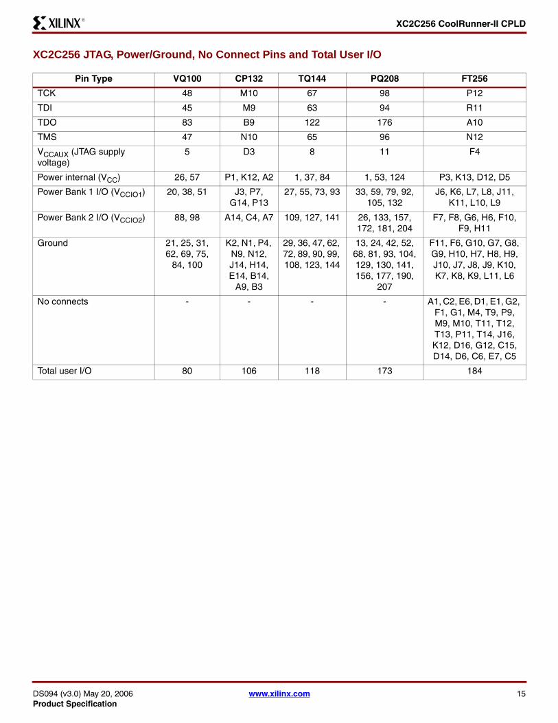
XC2C256 CoolRunner-II CPLDR
XC2C256 JTAG PowerGround No Connect Pins and Total User IO
Pin Type VQ100 CP132 TQ144 PQ208 FT256
TCK 48 M10 67 98 P12
TDI 45 M9 63 94 R11
TDO 83 B9 122 176 A10
TMS 47 N10 65 96 N12
VCCAUX (JTAG supply voltage)
5 D3 8 11 F4
Power internal (VCC) 26 57 P1 K12 A2 1 37 84 1 53 124 P3 K13 D12 D5
Power Bank 1 IO (VCCIO1) 20 38 51 J3 P7 G14 P13
27 55 73 93 33 59 79 92 105 132
J6 K6 L7 L8 J11 K11 L10 L9
Power Bank 2 IO (VCCIO2) 88 98 A14 C4 A7 109 127 141 26 133 157 172 181 204
F7 F8 G6 H6 F10 F9 H11
Ground 21 25 31 62 69 75
84 100
K2 N1 P4 N9 N12 J14 H14 E14 B14
A9 B3
29 36 47 62 72 89 90 99 108 123 144
13 24 42 52 68 81 93 104 129 130 141 156 177 190
207
F11 F6 G10 G7 G8 G9 H10 H7 H8 H9 J10 J7 J8 J9 K10 K7 K8 K9 L11 L6
No connects - - - - A1 C2 E6 D1 E1 G2 F1 G1 M4 T9 P9 M9 M10 T11 T12 T13 P11 T14 J16 K12 D16 G12 C15 D14 D6 C6 E7 C5
Total user IO 80 106 118 173 184
DS094 (v30) May 20 2006 wwwxilinxcom 15Product Specification
XC2C256 CoolRunner-II CPLDR
Ordering Information
Part NumberPinBall Spacing
θJA (CWatt)
θJC (CWatt) Package Type
Package Body Dimensions IO
Commercial (C)
Industrial (I)(1)
XC2C256-6VQ100C 05mm 431 109 Very Thin Quad Flat Pack
14mm x 14mm 80 C
XC2C256-7VQ100C 05mm 431 109 Very Thin Quad Flat Pack
14mm x 14mm 80 C
XC2C256-6CP132C 05mm 650 150 Chip Scale Package 8mm x 8mm 106 C
XC2C256-7CP132C 05mm 650 150 Chip Scale Package 8mm x 8mm 106 C
XC2C256-6TQ144C 05mm 372 72 Thin Quad Flat Pack 20mm x 20mm 118 C
XC2C256-7TQ144C 05mm 372 72 Thin Quad Flat Pack 20mm x 20mm 118 C
XC2C256-6PQ208C 05mm 369 97 Plastic Quad Flat Pack
28mm x 28mm 173 C
XC2C256-7PQ208C 05mm 369 97 Plastic Quad Flat Pack
28mm x 28mm 173 C
XC2C256-6FT256C 10mm 346 61 Fine Pitch Thin BGA 17mm x 17mm 184 C
XC2C256-7FT256C 10mm 346 61 Fine Pitch Thin BGA 17mm x 17mm 184 C
XC2C256-6VQG100C 05mm 431 109 Very Thin Quad Flat Pack Pb-free
14mm x 14mm 80 C
XC2C256-7VQG100C 05mm 431 109 Very Thin Quad Flat Pack Pb-free
14mm x 14mm 80 C
XC2C256-6CPG132C 05mm 650 150 Chip Scale Package Pb-free
8mm x 8mm 106 C
XC2C256-7CPG132C 05mm 650 150 Chip Scale Package Pb-free
8mm x 8mm 106 C
XC2C256-6TQG144C 05mm 372 72 Thin Quad Flat Pack Pb-free
20mm x 20mm 118 C
XC2C256-7TQG144C 05mm 372 72 Thin Quad Flat Pack Pb-free
20mm x 20mm 118 C
XC2C256-6PQG208C 05mm 369 97 Plastic Quad Flat Pack Pb-free
28mm x 28mm 173 C
XC2C256-7PQG208C 05mm 369 97 Plastic Quad Flat Pack Pb-free
28mm x 28mm 173 C
XC2C256-6FTG256C 10mm 346 61 Fine Pitch Thin BGA Pb-free
17mm x 17mm 184 C
XC2C256-7FTG256C 10mm 346 61 Fine Pitch Thin BGA Pb-free
17mm x 17mm 184 C
XC2C256-7VQ100I 05mm 431 109 Very Thin Quad Flat Pack
14mm x 14mm 80 I
XC2C256-7CP132I 05mm 650 150 Chip Scale Package 8mm x 8mm 106 I
XC2C256-7TQ144I 05mm 372 72 Thin Quad Flat Pack 20mm x 20mm 118 I
XC2C256-7PQ208I 05mm 369 97 Plastic Quad Flat Pack
28mm x 28mm 173 I
XC2C256-7FT256I 10mm 346 61 Fine Pitch Thin BGA 17mm x 17mm 184 I
16 wwwxilinxcom DS094 (v30) May 20 2006Product Specification
XC2C256 CoolRunner-II CPLDR
Device Part Marking
Figure 5 Sample Package with Part Marking
Note Due to the small size of chip scale packages the complete ordering part number cannot be included on the packagemarking Part marking on chip scale packages by line are
bull Line 1 = X (Xilinx logo) then truncated part numberbull Line 2 = Not related to device part numberbull Line 3 = Not related to device part number
1 Line 4 = Package code speed operating temperature three digits not related to device part number Package codes C5 = CP132 C6 = CPG132
XC2C256-7VQG100I 05mm 431 109 Very Thin Quad Flat Pack Pb-free
14mm x 14mm 80 I
XC2C256-7CPG132I 05mm 650 150 Chip Scale Package Pb-free
8mm x 8mm 106 I
XC2C256-7TQG144I 05mm 372 72 Thin Quad Flat Pack Pb-free
20mm x 20mm 118 I
XC2C256-7PQG208I 05mm 369 97 Plastic Quad Flat Pack Pb-free
28mm x 28mm 173 I
XC2C256-7FTG256I 10mm 346 61 Fine Pitch Thin BGA Pb-free
17mm x 17mm 184 I
Notes 1 C = Commercial (TA = 0degC to +70degC) I = Industrial (TA = ndash40degC to +85degC)
Part NumberPinBall Spacing
θJA (CWatt)
θJC (CWatt) Package Type
Package Body Dimensions IO
Commercial (C)
Industrial (I)(1)
Standard Example XC2C128 Device Speed Grade Package Type Number of Pins Temperature Range
-6 TQ C144 Pb-Free Example XC2C128 TQ G 144 C
Device Speed Grade Package Type Pb-FreeNumber of Pins
-6
Temperature Range
XC2Cxxx
TQ144
7C
Device Type
Package
Speed
Operating Range
This line not
related to device
part number
R
Part marking for non-chip scale package
DS094 (v30) May 20 2006 wwwxilinxcom 17Product Specification
XC2C256 CoolRunner-II CPLDR
Figure 6 VQ100 Very Thin Quad Flat Pack
VQ100Top View
GN
DIO
(3)
VC
CIO
2IO IO IO IO IO IO IO IO IO V
CC
IO2
IO IO IO GN
DT
DO
IO IO IO IO IO IO IO
VC
CIO
(2)
IO(5
)
IO IOG
ND
IO IO IO IO IO IOV
CC
IO1
IO IO IO IO IO IO TD
IIO
TM
ST
CK
IO IO
GNDIOIOIOIOIOGNDIOIOIOIOIOIOGNDIOIOIOIOVCCIOIOIOIOIOVCCIO1
IO(1)IO(1)IO(1)IO(1)VAUX
IOIOIOIOIOIOIOIOIOIOIOIOIOIO
VCCIO1GND
IO(2)IO(2)IO(4)GND
12345678910111213141516171819202122232425
75747372717069686766656463626160595857565554535251
26 27 28 29 30 31 32 33 34 35 36 37 38 39 40 41 42 43 44 45 46 47 48 49 50
100 99 98 97 96 95 94 93 92 91 90 89 88 87 86 85 84 83 82 81 80 79 78 77 76
(1) - Global Output Enable(2) - Global Clock(3) - Global SetReset(4) - Clock Divide Reset(5) - Data Gate
18 wwwxilinxcom DS094 (v30) May 20 2006Product Specification
XC2C256 CoolRunner-II CPLDR
Figure 7 CP132 Chip Scale Package
CP132Bottom View
P
N
M
L
K
J
H
G
F
E
D
C
B
A
1 2 3 4 5 6 7 8 9 10 11 12 13 14
VCC VCCIO1 VCCIO1GNDIO IO IO IO IO IO IO IO IOIO(5)
IO IOVAUX IO IOIO
IO IOIO IO IOIO
IO IOIO IO VCCIO1IO
IO IOIO IO GNDIO
IO IOIO IO GNDIO
IO IOVCCIO1 IO GNDIO
IO IOIO(2) VCC IOGND
IO IOIO IO IOIO(2)
IO(1) VCCIO2 IOIOIO(3) IO IO IO GND IO IO IO VCCIO2VCC
IO IO IOIOGND IO IO IO TDO IO IO IO GNDIO(1)
IO IO IOVCCIO2IO(1) IO IO IO IO IO IO IO IOIO(1)
IO IO IOIOIO IO IO IO TDI TCK IO IO IOIO(4)
GND IO IOIOIO IO IO IO GND TMS IO GND IOIO(2)
(1) - Global Output Enable(2) - Global Clock(3) - Global SetReset(4) - Clock Divide Reset(5) - DataGATE Enable
DS094 (v30) May 20 2006 wwwxilinxcom 19Product Specification
XC2C256 CoolRunner-II CPLDR
Figure 8 TQ144 Thin Quad Flat Pack
VCCIO(1)
IO(1)
IOIO(1)
IO(1)
IOVAUX
IOIOIOIOIOIOIOIOIOIOIOIOIOIOIOIOIOIO
VCCIO1IO
GNDIO(2)
IOIO(2)
IOIO
IO(4)
GND
123456789101112131415161718192021222324252627282930313233343536
TQ144Top View
VC
CIO
(2)
IO(5
)
IO IO IO IO IO IO IOG
ND
IO IO IO IO IO IO IOV
CC
IO1
IO IO IO IO IO IOG
ND
TD
IIO
TM
SIO
TC
KIO IO IO IO
GN
D
108107106105104103102101100999897969594939291908988878685848382818079787776757473
37 38 39 40 41 42 43 44 45 46 47 48 49 50 51 52 53 54 55 56 57 58 59 60 61 62 63 64 65 66 67 68 69 70 71 72
144
143
142
141
140
139
138
137
136
135
134
133
132
131
130
129
128
127
126
125
124
123
122
121
120
119
118
117
116
115
114
113
112
111
110
109
GNDIOIOIOIOIOIOIOIOGNDIOIOIOIOIOVCCIO1IOIOGNDGNDIOIOIOIOVCCIOIOIOIOIOIOIOIOIOIOVCCIO1
GN
DIO
(3)
IO VC
CIO
2IO IO IO IO IO IO IO IO IO IO IO IO IO V
CC
IO2
IO IO IO GN
DT
DO
IO IO IO IO IO IO IO IO IO IO IO IO VC
CIO
2
(1) - Global Output Enable(2) - Global Clock(3) - Global SetReset(4) - Clock Divide Reset(5) - DataGATE Enable
20 wwwxilinxcom DS094 (v30) May 20 2006Product Specification
XC2C256 CoolRunner-II CPLDR
Figure 9 PQ208 Quad Flat Package
VCCIO
IO(1)IO
IO(1)IO
IO(1)IO
IO(1)IO
VAUXIO
GNDIOIOIOIOIOIOIOIOIOIO
GNDIO
VCCIO2IOIOIOIOIOIO
VCCIO1IOIOIOIOIOIOIOIO
GNDIO
IO(2)IO
IO(2)IOIOIOIO
IO(4)GND
PQ208Top View
VC
CI
OI
O(2
)I
OI
OI
O(5
)V
CC
IO1
IO
IO
IO
IO
IO
IO
IO
IO
GN
DI
OI
OI
OI
OI
OI
OI
OI
OI
OI
OV
CC
IO1
IO
GN
DI
OI
OI
OI
OI
OI
OI
OI
OI
OI
OV
CC
IO1
GN
DT
DI
IO
TM
SI
OT
CK
IO
IO
IO
IO
IO
GN
D
(1) - Global Output Enable(2) - Global Clock(3) - Global SetReset(4) - Clock Divide Reset(5) - DataGATE Enable
GNDIOIOIOIOIOIOIOIOIOIOIOIOIOIOGNDIOIOIOIOIOIOIOVCCIO2VCCIO1IOGNDGNDIOIOIOIOVCCIOIOIOIOIOIOIOIOIOIOIOIOIOIOIOIOIOIOVCCIO1
IO GN
DIO
(3)
IO VC
CIO
2IO IO IO IO IO IO IO IO IO IO IO IO IO G
ND
IO IO IO IO IO IO IO IO VC
CIO
2IO IO IO G
ND
TD
OIO IO IO V
CC
IO2
IO IO IO IO IO IO IO IO IO IO IO IO IO IO VC
CIO
2
12345678910111213141516171819202122232425262728293031323334353637383940414243444546474849505152
53 54 55 56 57 58 59 60 61 62 63 64 65 66 67 68 69 70 71 72 73 74 75 76 77 78 79 80 81 82 83 84 85 86 87 88 89 90 91 92 93 94 95 96 97 98 99 100
101
102
103
104
156155154153152151150149148147146145144143142141140139138137136135134133132131130129128127126125124123122121120119118117116115114113112111110109108107106105
208
207
206
205
204
203
202
201
200
199
198
197
196
195
194
193
192
191
190
189
188
187
186
185
184
183
182
181
180
179
178
177
176
175
174
173
172
171
170
169
168
167
166
165
164
163
162
161
160
159
158
157
DS094 (v30) May 20 2006 wwwxilinxcom 21Product Specification
XC2C256 CoolRunner-II CPLDR
Warranty DisclaimerTHESE PRODUCTS ARE SUBJECT TO THE TERMS OF THE XILINX LIMITED WARRANTY WHICH CAN BE VIEWEDAT httpwwwxilinxcomwarrantyhtm THIS LIMITED WARRANTY DOES NOT EXTEND TO ANY USE OF THEPRODUCTS IN AN APPLICATION OR ENVIRONMENT THAT IS NOT WITHIN THE SPECIFICATIONS STATED ON THETHEN-CURRENT XILINX DATA SHEET FOR THE PRODUCTS PRODUCTS ARE NOT DESIGNED TO BE FAIL-SAFEAND ARE NOT WARRANTED FOR USE IN APPLICATIONS THAT POSE A RISK OF PHYSICAL HARM OR LOSS OFLIFE USE OF PRODUCTS IN SUCH APPLICATIONS IS FULLY AT THE RISK OF CUSTOMER SUBJECT TOAPPLICABLE LAWS AND REGULATIONS
Figure 10 FT256 Fine Pitch Thin BGA
FT256 Bottom View
A
B
C
D
E
F
G
H
J
K
L
M
N
P
R
T
16 15 14 13 12 11 10 9 8 7 6 5 4 3 2 1
IO TDO IOIOIO IO IO IO IO IO IO IO IO IO NCIO
IO IO IOIOIO IO IO IO IO IO IO IO IO IO IOIO
IO IO IO(3)IOIO IO IO IO IO IO NC NC IO NC IONC
NC IO IO(1)IONC VCC IO IO IO IO NC VCC IO(1) IO NCIO
IO IO IOIOIO IO IO IO IO NC NC IO(1) IO(1) IO NCIO
IO VCCIO2 VAUXIOIO IO GND VCCIO2 VCCIO2 VCCIO2 GND IO IO IO NCIO
IO GND IOIOIO NC IO GND GND GND VCCIO2 IO IO NC NCIO
IO GND IOIOIO IO VCCIO2 GND GND GND VCCIO2 IO IO IO IOIO
NC GND IOIOIO IO VCCIO1 GND GND GND VCCIO1 IO IO IO IOIO
IO GND IOVCCIO NC VCCIO1 GND GND GND VCCIO1 IO IO IO IOIO
IO VCCIO1 IOIOIO IO GND VCCIO1 VCCIO1 VCCIO1 GND IO IO IO IOIO
IO NC NCIOIO IO IO NC IO IO IO IO IO(2) IO(2) IOIO
IO IO IOIOIO TMS IO IO IO IO IO IO IO IO IOIO
IO IO IOIOIO TCK NC NC IO IO IO IO(2) VCC IO(4) IOIO
IO IO IOIOIO IO TDI IO IO IO IO IO IO IO IOIO
IO IO IONCNC NC NC NC IO IO IO IO IO IO(5) IOIO
(1) - Global Output Enable(2) - Global Clock(3) - Global SetReset(4) - Clock Divide Reset(5) - DataGATE Enable
22 wwwxilinxcom DS094 (v30) May 20 2006Product Specification
XC2C256 CoolRunner-II CPLDR
Additional InformationAdditional information is available for the following CoolRunner-II topics
bull XAPP784 Bulletproof CPLD Design Practicesbull XAPP375 Timing Model bull XAPP376 Logic Engine bull XAPP378 Advanced Features bull XAPP382 IO Characteristics bull XAPP389 Powering CoolRunner-II bull XAPP399 Assigning VREF Pins
To access these and all application notes with their associ-ated reference designs click the following link and scrolldown the page until you find the document you want
CoolRunner-II Data Sheets and Application Notes
Device Packages
Revision HistoryThe following table shows the revision history for this document
Date Version Revision
050902 10 Initial Xilinx release
051302 11 Updated AC Electrical Characteristics and added new parameters
103102 12 Corrected package user IO added Voltage Referenced DC tables
031703 20 Added Characterization numbers for product release and device part marking
040203 21 Updated TSOL max from 260 to 220 Changed ICCSB units from mA to μA
012604 22 Updated Device Part Marking Updated links and Tsol
022604 23 Corrected Theta JC value on XC2C256-7TQ144
080304 24 Pb-free documentation
081904 25 Changes to ICCSB maximum specifications in DC Electrical Characteristics table on page 3
100104 26 Add Asynchronous PresetReset Pulse Width specification to AC Electrical Characteristics
030705 27 Removed -5 speed grade Changes to Table 1 IO Standards
062805 28 Move to Product Specification Change to TIN25 TOUT25 TIN33 and TOUT33 for -7 speed grade
032006 29 Add Warranty Disclaimer Add note to Pin Description table that GTS GSR and GCK pins can be used for general purpose IO
52006 30 Moved TCONFIG specification values from MIN column to MAX column page 7
DS094 (v30) May 20 2006 wwwxilinxcom 23Product Specification
- Features
- Description
- RealDigital Design Technology
- Supported IO Standards
- Absolute Maximum Ratings
- Recommended Operating Conditions
- DC Electrical Characteristics (Over Recommended Operating Conditions)
- LVCMOS 33V and LVTTL 33V DC Voltage Specifications
- LVCMOS 25V DC Voltage Specifications
- LVCMOS 18V DC Voltage Specifications
- LVCMOS 15V DC Voltage Specifications(1)
- Schmitt Trigger Input DC Voltage Specifications
- SSTL2-1 DC Voltage Specifications
- SSTL3-1 DC Voltage Specifications
- HSTL1 DC Voltage Specifications
- AC Electrical Characteristics Over Recommended Operating Conditions
- Internal Timing Parameters
-
- Switching Characteristics
- AC Test Circuit
-
- Pin Descriptions
-
- XC2C256 JTAG PowerGround No Connect Pins and Total User IO
-
- Warranty Disclaimer
- Additional Information
- Revision History
-
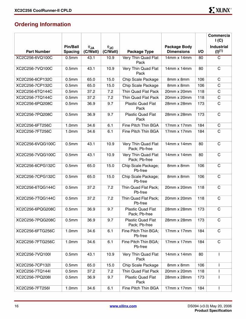
XC2C256 CoolRunner-II CPLDR
Device Part Marking
Figure 5 Sample Package with Part Marking
Note Due to the small size of chip scale packages the complete ordering part number cannot be included on the packagemarking Part marking on chip scale packages by line are
bull Line 1 = X (Xilinx logo) then truncated part numberbull Line 2 = Not related to device part numberbull Line 3 = Not related to device part number
1 Line 4 = Package code speed operating temperature three digits not related to device part number Package codes C5 = CP132 C6 = CPG132
XC2C256-7VQG100I 05mm 431 109 Very Thin Quad Flat Pack Pb-free
14mm x 14mm 80 I
XC2C256-7CPG132I 05mm 650 150 Chip Scale Package Pb-free
8mm x 8mm 106 I
XC2C256-7TQG144I 05mm 372 72 Thin Quad Flat Pack Pb-free
20mm x 20mm 118 I
XC2C256-7PQG208I 05mm 369 97 Plastic Quad Flat Pack Pb-free
28mm x 28mm 173 I
XC2C256-7FTG256I 10mm 346 61 Fine Pitch Thin BGA Pb-free
17mm x 17mm 184 I
Notes 1 C = Commercial (TA = 0degC to +70degC) I = Industrial (TA = ndash40degC to +85degC)
Part NumberPinBall Spacing
θJA (CWatt)
θJC (CWatt) Package Type
Package Body Dimensions IO
Commercial (C)
Industrial (I)(1)
Standard Example XC2C128 Device Speed Grade Package Type Number of Pins Temperature Range
-6 TQ C144 Pb-Free Example XC2C128 TQ G 144 C
Device Speed Grade Package Type Pb-FreeNumber of Pins
-6
Temperature Range
XC2Cxxx
TQ144
7C
Device Type
Package
Speed
Operating Range
This line not
related to device
part number
R
Part marking for non-chip scale package
DS094 (v30) May 20 2006 wwwxilinxcom 17Product Specification
XC2C256 CoolRunner-II CPLDR
Figure 6 VQ100 Very Thin Quad Flat Pack
VQ100Top View
GN
DIO
(3)
VC
CIO
2IO IO IO IO IO IO IO IO IO V
CC
IO2
IO IO IO GN
DT
DO
IO IO IO IO IO IO IO
VC
CIO
(2)
IO(5
)
IO IOG
ND
IO IO IO IO IO IOV
CC
IO1
IO IO IO IO IO IO TD
IIO
TM
ST
CK
IO IO
GNDIOIOIOIOIOGNDIOIOIOIOIOIOGNDIOIOIOIOVCCIOIOIOIOIOVCCIO1
IO(1)IO(1)IO(1)IO(1)VAUX
IOIOIOIOIOIOIOIOIOIOIOIOIOIO
VCCIO1GND
IO(2)IO(2)IO(4)GND
12345678910111213141516171819202122232425
75747372717069686766656463626160595857565554535251
26 27 28 29 30 31 32 33 34 35 36 37 38 39 40 41 42 43 44 45 46 47 48 49 50
100 99 98 97 96 95 94 93 92 91 90 89 88 87 86 85 84 83 82 81 80 79 78 77 76
(1) - Global Output Enable(2) - Global Clock(3) - Global SetReset(4) - Clock Divide Reset(5) - Data Gate
18 wwwxilinxcom DS094 (v30) May 20 2006Product Specification
XC2C256 CoolRunner-II CPLDR
Figure 7 CP132 Chip Scale Package
CP132Bottom View
P
N
M
L
K
J
H
G
F
E
D
C
B
A
1 2 3 4 5 6 7 8 9 10 11 12 13 14
VCC VCCIO1 VCCIO1GNDIO IO IO IO IO IO IO IO IOIO(5)
IO IOVAUX IO IOIO
IO IOIO IO IOIO
IO IOIO IO VCCIO1IO
IO IOIO IO GNDIO
IO IOIO IO GNDIO
IO IOVCCIO1 IO GNDIO
IO IOIO(2) VCC IOGND
IO IOIO IO IOIO(2)
IO(1) VCCIO2 IOIOIO(3) IO IO IO GND IO IO IO VCCIO2VCC
IO IO IOIOGND IO IO IO TDO IO IO IO GNDIO(1)
IO IO IOVCCIO2IO(1) IO IO IO IO IO IO IO IOIO(1)
IO IO IOIOIO IO IO IO TDI TCK IO IO IOIO(4)
GND IO IOIOIO IO IO IO GND TMS IO GND IOIO(2)
(1) - Global Output Enable(2) - Global Clock(3) - Global SetReset(4) - Clock Divide Reset(5) - DataGATE Enable
DS094 (v30) May 20 2006 wwwxilinxcom 19Product Specification
XC2C256 CoolRunner-II CPLDR
Figure 8 TQ144 Thin Quad Flat Pack
VCCIO(1)
IO(1)
IOIO(1)
IO(1)
IOVAUX
IOIOIOIOIOIOIOIOIOIOIOIOIOIOIOIOIOIO
VCCIO1IO
GNDIO(2)
IOIO(2)
IOIO
IO(4)
GND
123456789101112131415161718192021222324252627282930313233343536
TQ144Top View
VC
CIO
(2)
IO(5
)
IO IO IO IO IO IO IOG
ND
IO IO IO IO IO IO IOV
CC
IO1
IO IO IO IO IO IOG
ND
TD
IIO
TM
SIO
TC
KIO IO IO IO
GN
D
108107106105104103102101100999897969594939291908988878685848382818079787776757473
37 38 39 40 41 42 43 44 45 46 47 48 49 50 51 52 53 54 55 56 57 58 59 60 61 62 63 64 65 66 67 68 69 70 71 72
144
143
142
141
140
139
138
137
136
135
134
133
132
131
130
129
128
127
126
125
124
123
122
121
120
119
118
117
116
115
114
113
112
111
110
109
GNDIOIOIOIOIOIOIOIOGNDIOIOIOIOIOVCCIO1IOIOGNDGNDIOIOIOIOVCCIOIOIOIOIOIOIOIOIOIOVCCIO1
GN
DIO
(3)
IO VC
CIO
2IO IO IO IO IO IO IO IO IO IO IO IO IO V
CC
IO2
IO IO IO GN
DT
DO
IO IO IO IO IO IO IO IO IO IO IO IO VC
CIO
2
(1) - Global Output Enable(2) - Global Clock(3) - Global SetReset(4) - Clock Divide Reset(5) - DataGATE Enable
20 wwwxilinxcom DS094 (v30) May 20 2006Product Specification
XC2C256 CoolRunner-II CPLDR
Figure 9 PQ208 Quad Flat Package
VCCIO
IO(1)IO
IO(1)IO
IO(1)IO
IO(1)IO
VAUXIO
GNDIOIOIOIOIOIOIOIOIOIO
GNDIO
VCCIO2IOIOIOIOIOIO
VCCIO1IOIOIOIOIOIOIOIO
GNDIO
IO(2)IO
IO(2)IOIOIOIO
IO(4)GND
PQ208Top View
VC
CI
OI
O(2
)I
OI
OI
O(5
)V
CC
IO1
IO
IO
IO
IO
IO
IO
IO
IO
GN
DI
OI
OI
OI
OI
OI
OI
OI
OI
OI
OV
CC
IO1
IO
GN
DI
OI
OI
OI
OI
OI
OI
OI
OI
OI
OV
CC
IO1
GN
DT
DI
IO
TM
SI
OT
CK
IO
IO
IO
IO
IO
GN
D
(1) - Global Output Enable(2) - Global Clock(3) - Global SetReset(4) - Clock Divide Reset(5) - DataGATE Enable
GNDIOIOIOIOIOIOIOIOIOIOIOIOIOIOGNDIOIOIOIOIOIOIOVCCIO2VCCIO1IOGNDGNDIOIOIOIOVCCIOIOIOIOIOIOIOIOIOIOIOIOIOIOIOIOIOIOVCCIO1
IO GN
DIO
(3)
IO VC
CIO
2IO IO IO IO IO IO IO IO IO IO IO IO IO G
ND
IO IO IO IO IO IO IO IO VC
CIO
2IO IO IO G
ND
TD
OIO IO IO V
CC
IO2
IO IO IO IO IO IO IO IO IO IO IO IO IO IO VC
CIO
2
12345678910111213141516171819202122232425262728293031323334353637383940414243444546474849505152
53 54 55 56 57 58 59 60 61 62 63 64 65 66 67 68 69 70 71 72 73 74 75 76 77 78 79 80 81 82 83 84 85 86 87 88 89 90 91 92 93 94 95 96 97 98 99 100
101
102
103
104
156155154153152151150149148147146145144143142141140139138137136135134133132131130129128127126125124123122121120119118117116115114113112111110109108107106105
208
207
206
205
204
203
202
201
200
199
198
197
196
195
194
193
192
191
190
189
188
187
186
185
184
183
182
181
180
179
178
177
176
175
174
173
172
171
170
169
168
167
166
165
164
163
162
161
160
159
158
157
DS094 (v30) May 20 2006 wwwxilinxcom 21Product Specification
XC2C256 CoolRunner-II CPLDR
Warranty DisclaimerTHESE PRODUCTS ARE SUBJECT TO THE TERMS OF THE XILINX LIMITED WARRANTY WHICH CAN BE VIEWEDAT httpwwwxilinxcomwarrantyhtm THIS LIMITED WARRANTY DOES NOT EXTEND TO ANY USE OF THEPRODUCTS IN AN APPLICATION OR ENVIRONMENT THAT IS NOT WITHIN THE SPECIFICATIONS STATED ON THETHEN-CURRENT XILINX DATA SHEET FOR THE PRODUCTS PRODUCTS ARE NOT DESIGNED TO BE FAIL-SAFEAND ARE NOT WARRANTED FOR USE IN APPLICATIONS THAT POSE A RISK OF PHYSICAL HARM OR LOSS OFLIFE USE OF PRODUCTS IN SUCH APPLICATIONS IS FULLY AT THE RISK OF CUSTOMER SUBJECT TOAPPLICABLE LAWS AND REGULATIONS
Figure 10 FT256 Fine Pitch Thin BGA
FT256 Bottom View
A
B
C
D
E
F
G
H
J
K
L
M
N
P
R
T
16 15 14 13 12 11 10 9 8 7 6 5 4 3 2 1
IO TDO IOIOIO IO IO IO IO IO IO IO IO IO NCIO
IO IO IOIOIO IO IO IO IO IO IO IO IO IO IOIO
IO IO IO(3)IOIO IO IO IO IO IO NC NC IO NC IONC
NC IO IO(1)IONC VCC IO IO IO IO NC VCC IO(1) IO NCIO
IO IO IOIOIO IO IO IO IO NC NC IO(1) IO(1) IO NCIO
IO VCCIO2 VAUXIOIO IO GND VCCIO2 VCCIO2 VCCIO2 GND IO IO IO NCIO
IO GND IOIOIO NC IO GND GND GND VCCIO2 IO IO NC NCIO
IO GND IOIOIO IO VCCIO2 GND GND GND VCCIO2 IO IO IO IOIO
NC GND IOIOIO IO VCCIO1 GND GND GND VCCIO1 IO IO IO IOIO
IO GND IOVCCIO NC VCCIO1 GND GND GND VCCIO1 IO IO IO IOIO
IO VCCIO1 IOIOIO IO GND VCCIO1 VCCIO1 VCCIO1 GND IO IO IO IOIO
IO NC NCIOIO IO IO NC IO IO IO IO IO(2) IO(2) IOIO
IO IO IOIOIO TMS IO IO IO IO IO IO IO IO IOIO
IO IO IOIOIO TCK NC NC IO IO IO IO(2) VCC IO(4) IOIO
IO IO IOIOIO IO TDI IO IO IO IO IO IO IO IOIO
IO IO IONCNC NC NC NC IO IO IO IO IO IO(5) IOIO
(1) - Global Output Enable(2) - Global Clock(3) - Global SetReset(4) - Clock Divide Reset(5) - DataGATE Enable
22 wwwxilinxcom DS094 (v30) May 20 2006Product Specification
XC2C256 CoolRunner-II CPLDR
Additional InformationAdditional information is available for the following CoolRunner-II topics
bull XAPP784 Bulletproof CPLD Design Practicesbull XAPP375 Timing Model bull XAPP376 Logic Engine bull XAPP378 Advanced Features bull XAPP382 IO Characteristics bull XAPP389 Powering CoolRunner-II bull XAPP399 Assigning VREF Pins
To access these and all application notes with their associ-ated reference designs click the following link and scrolldown the page until you find the document you want
CoolRunner-II Data Sheets and Application Notes
Device Packages
Revision HistoryThe following table shows the revision history for this document
Date Version Revision
050902 10 Initial Xilinx release
051302 11 Updated AC Electrical Characteristics and added new parameters
103102 12 Corrected package user IO added Voltage Referenced DC tables
031703 20 Added Characterization numbers for product release and device part marking
040203 21 Updated TSOL max from 260 to 220 Changed ICCSB units from mA to μA
012604 22 Updated Device Part Marking Updated links and Tsol
022604 23 Corrected Theta JC value on XC2C256-7TQ144
080304 24 Pb-free documentation
081904 25 Changes to ICCSB maximum specifications in DC Electrical Characteristics table on page 3
100104 26 Add Asynchronous PresetReset Pulse Width specification to AC Electrical Characteristics
030705 27 Removed -5 speed grade Changes to Table 1 IO Standards
062805 28 Move to Product Specification Change to TIN25 TOUT25 TIN33 and TOUT33 for -7 speed grade
032006 29 Add Warranty Disclaimer Add note to Pin Description table that GTS GSR and GCK pins can be used for general purpose IO
52006 30 Moved TCONFIG specification values from MIN column to MAX column page 7
DS094 (v30) May 20 2006 wwwxilinxcom 23Product Specification
- Features
- Description
- RealDigital Design Technology
- Supported IO Standards
- Absolute Maximum Ratings
- Recommended Operating Conditions
- DC Electrical Characteristics (Over Recommended Operating Conditions)
- LVCMOS 33V and LVTTL 33V DC Voltage Specifications
- LVCMOS 25V DC Voltage Specifications
- LVCMOS 18V DC Voltage Specifications
- LVCMOS 15V DC Voltage Specifications(1)
- Schmitt Trigger Input DC Voltage Specifications
- SSTL2-1 DC Voltage Specifications
- SSTL3-1 DC Voltage Specifications
- HSTL1 DC Voltage Specifications
- AC Electrical Characteristics Over Recommended Operating Conditions
- Internal Timing Parameters
-
- Switching Characteristics
- AC Test Circuit
-
- Pin Descriptions
-
- XC2C256 JTAG PowerGround No Connect Pins and Total User IO
-
- Warranty Disclaimer
- Additional Information
- Revision History
-
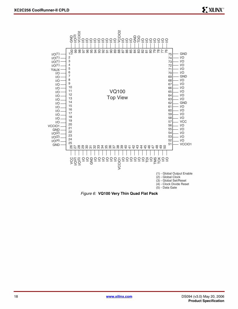
XC2C256 CoolRunner-II CPLDR
Figure 6 VQ100 Very Thin Quad Flat Pack
VQ100Top View
GN
DIO
(3)
VC
CIO
2IO IO IO IO IO IO IO IO IO V
CC
IO2
IO IO IO GN
DT
DO
IO IO IO IO IO IO IO
VC
CIO
(2)
IO(5
)
IO IOG
ND
IO IO IO IO IO IOV
CC
IO1
IO IO IO IO IO IO TD
IIO
TM
ST
CK
IO IO
GNDIOIOIOIOIOGNDIOIOIOIOIOIOGNDIOIOIOIOVCCIOIOIOIOIOVCCIO1
IO(1)IO(1)IO(1)IO(1)VAUX
IOIOIOIOIOIOIOIOIOIOIOIOIOIO
VCCIO1GND
IO(2)IO(2)IO(4)GND
12345678910111213141516171819202122232425
75747372717069686766656463626160595857565554535251
26 27 28 29 30 31 32 33 34 35 36 37 38 39 40 41 42 43 44 45 46 47 48 49 50
100 99 98 97 96 95 94 93 92 91 90 89 88 87 86 85 84 83 82 81 80 79 78 77 76
(1) - Global Output Enable(2) - Global Clock(3) - Global SetReset(4) - Clock Divide Reset(5) - Data Gate
18 wwwxilinxcom DS094 (v30) May 20 2006Product Specification
XC2C256 CoolRunner-II CPLDR
Figure 7 CP132 Chip Scale Package
CP132Bottom View
P
N
M
L
K
J
H
G
F
E
D
C
B
A
1 2 3 4 5 6 7 8 9 10 11 12 13 14
VCC VCCIO1 VCCIO1GNDIO IO IO IO IO IO IO IO IOIO(5)
IO IOVAUX IO IOIO
IO IOIO IO IOIO
IO IOIO IO VCCIO1IO
IO IOIO IO GNDIO
IO IOIO IO GNDIO
IO IOVCCIO1 IO GNDIO
IO IOIO(2) VCC IOGND
IO IOIO IO IOIO(2)
IO(1) VCCIO2 IOIOIO(3) IO IO IO GND IO IO IO VCCIO2VCC
IO IO IOIOGND IO IO IO TDO IO IO IO GNDIO(1)
IO IO IOVCCIO2IO(1) IO IO IO IO IO IO IO IOIO(1)
IO IO IOIOIO IO IO IO TDI TCK IO IO IOIO(4)
GND IO IOIOIO IO IO IO GND TMS IO GND IOIO(2)
(1) - Global Output Enable(2) - Global Clock(3) - Global SetReset(4) - Clock Divide Reset(5) - DataGATE Enable
DS094 (v30) May 20 2006 wwwxilinxcom 19Product Specification
XC2C256 CoolRunner-II CPLDR
Figure 8 TQ144 Thin Quad Flat Pack
VCCIO(1)
IO(1)
IOIO(1)
IO(1)
IOVAUX
IOIOIOIOIOIOIOIOIOIOIOIOIOIOIOIOIOIO
VCCIO1IO
GNDIO(2)
IOIO(2)
IOIO
IO(4)
GND
123456789101112131415161718192021222324252627282930313233343536
TQ144Top View
VC
CIO
(2)
IO(5
)
IO IO IO IO IO IO IOG
ND
IO IO IO IO IO IO IOV
CC
IO1
IO IO IO IO IO IOG
ND
TD
IIO
TM
SIO
TC
KIO IO IO IO
GN
D
108107106105104103102101100999897969594939291908988878685848382818079787776757473
37 38 39 40 41 42 43 44 45 46 47 48 49 50 51 52 53 54 55 56 57 58 59 60 61 62 63 64 65 66 67 68 69 70 71 72
144
143
142
141
140
139
138
137
136
135
134
133
132
131
130
129
128
127
126
125
124
123
122
121
120
119
118
117
116
115
114
113
112
111
110
109
GNDIOIOIOIOIOIOIOIOGNDIOIOIOIOIOVCCIO1IOIOGNDGNDIOIOIOIOVCCIOIOIOIOIOIOIOIOIOIOVCCIO1
GN
DIO
(3)
IO VC
CIO
2IO IO IO IO IO IO IO IO IO IO IO IO IO V
CC
IO2
IO IO IO GN
DT
DO
IO IO IO IO IO IO IO IO IO IO IO IO VC
CIO
2
(1) - Global Output Enable(2) - Global Clock(3) - Global SetReset(4) - Clock Divide Reset(5) - DataGATE Enable
20 wwwxilinxcom DS094 (v30) May 20 2006Product Specification
XC2C256 CoolRunner-II CPLDR
Figure 9 PQ208 Quad Flat Package
VCCIO
IO(1)IO
IO(1)IO
IO(1)IO
IO(1)IO
VAUXIO
GNDIOIOIOIOIOIOIOIOIOIO
GNDIO
VCCIO2IOIOIOIOIOIO
VCCIO1IOIOIOIOIOIOIOIO
GNDIO
IO(2)IO
IO(2)IOIOIOIO
IO(4)GND
PQ208Top View
VC
CI
OI
O(2
)I
OI
OI
O(5
)V
CC
IO1
IO
IO
IO
IO
IO
IO
IO
IO
GN
DI
OI
OI
OI
OI
OI
OI
OI
OI
OI
OV
CC
IO1
IO
GN
DI
OI
OI
OI
OI
OI
OI
OI
OI
OI
OV
CC
IO1
GN
DT
DI
IO
TM
SI
OT
CK
IO
IO
IO
IO
IO
GN
D
(1) - Global Output Enable(2) - Global Clock(3) - Global SetReset(4) - Clock Divide Reset(5) - DataGATE Enable
GNDIOIOIOIOIOIOIOIOIOIOIOIOIOIOGNDIOIOIOIOIOIOIOVCCIO2VCCIO1IOGNDGNDIOIOIOIOVCCIOIOIOIOIOIOIOIOIOIOIOIOIOIOIOIOIOIOVCCIO1
IO GN
DIO
(3)
IO VC
CIO
2IO IO IO IO IO IO IO IO IO IO IO IO IO G
ND
IO IO IO IO IO IO IO IO VC
CIO
2IO IO IO G
ND
TD
OIO IO IO V
CC
IO2
IO IO IO IO IO IO IO IO IO IO IO IO IO IO VC
CIO
2
12345678910111213141516171819202122232425262728293031323334353637383940414243444546474849505152
53 54 55 56 57 58 59 60 61 62 63 64 65 66 67 68 69 70 71 72 73 74 75 76 77 78 79 80 81 82 83 84 85 86 87 88 89 90 91 92 93 94 95 96 97 98 99 100
101
102
103
104
156155154153152151150149148147146145144143142141140139138137136135134133132131130129128127126125124123122121120119118117116115114113112111110109108107106105
208
207
206
205
204
203
202
201
200
199
198
197
196
195
194
193
192
191
190
189
188
187
186
185
184
183
182
181
180
179
178
177
176
175
174
173
172
171
170
169
168
167
166
165
164
163
162
161
160
159
158
157
DS094 (v30) May 20 2006 wwwxilinxcom 21Product Specification
XC2C256 CoolRunner-II CPLDR
Warranty DisclaimerTHESE PRODUCTS ARE SUBJECT TO THE TERMS OF THE XILINX LIMITED WARRANTY WHICH CAN BE VIEWEDAT httpwwwxilinxcomwarrantyhtm THIS LIMITED WARRANTY DOES NOT EXTEND TO ANY USE OF THEPRODUCTS IN AN APPLICATION OR ENVIRONMENT THAT IS NOT WITHIN THE SPECIFICATIONS STATED ON THETHEN-CURRENT XILINX DATA SHEET FOR THE PRODUCTS PRODUCTS ARE NOT DESIGNED TO BE FAIL-SAFEAND ARE NOT WARRANTED FOR USE IN APPLICATIONS THAT POSE A RISK OF PHYSICAL HARM OR LOSS OFLIFE USE OF PRODUCTS IN SUCH APPLICATIONS IS FULLY AT THE RISK OF CUSTOMER SUBJECT TOAPPLICABLE LAWS AND REGULATIONS
Figure 10 FT256 Fine Pitch Thin BGA
FT256 Bottom View
A
B
C
D
E
F
G
H
J
K
L
M
N
P
R
T
16 15 14 13 12 11 10 9 8 7 6 5 4 3 2 1
IO TDO IOIOIO IO IO IO IO IO IO IO IO IO NCIO
IO IO IOIOIO IO IO IO IO IO IO IO IO IO IOIO
IO IO IO(3)IOIO IO IO IO IO IO NC NC IO NC IONC
NC IO IO(1)IONC VCC IO IO IO IO NC VCC IO(1) IO NCIO
IO IO IOIOIO IO IO IO IO NC NC IO(1) IO(1) IO NCIO
IO VCCIO2 VAUXIOIO IO GND VCCIO2 VCCIO2 VCCIO2 GND IO IO IO NCIO
IO GND IOIOIO NC IO GND GND GND VCCIO2 IO IO NC NCIO
IO GND IOIOIO IO VCCIO2 GND GND GND VCCIO2 IO IO IO IOIO
NC GND IOIOIO IO VCCIO1 GND GND GND VCCIO1 IO IO IO IOIO
IO GND IOVCCIO NC VCCIO1 GND GND GND VCCIO1 IO IO IO IOIO
IO VCCIO1 IOIOIO IO GND VCCIO1 VCCIO1 VCCIO1 GND IO IO IO IOIO
IO NC NCIOIO IO IO NC IO IO IO IO IO(2) IO(2) IOIO
IO IO IOIOIO TMS IO IO IO IO IO IO IO IO IOIO
IO IO IOIOIO TCK NC NC IO IO IO IO(2) VCC IO(4) IOIO
IO IO IOIOIO IO TDI IO IO IO IO IO IO IO IOIO
IO IO IONCNC NC NC NC IO IO IO IO IO IO(5) IOIO
(1) - Global Output Enable(2) - Global Clock(3) - Global SetReset(4) - Clock Divide Reset(5) - DataGATE Enable
22 wwwxilinxcom DS094 (v30) May 20 2006Product Specification
XC2C256 CoolRunner-II CPLDR
Additional InformationAdditional information is available for the following CoolRunner-II topics
bull XAPP784 Bulletproof CPLD Design Practicesbull XAPP375 Timing Model bull XAPP376 Logic Engine bull XAPP378 Advanced Features bull XAPP382 IO Characteristics bull XAPP389 Powering CoolRunner-II bull XAPP399 Assigning VREF Pins
To access these and all application notes with their associ-ated reference designs click the following link and scrolldown the page until you find the document you want
CoolRunner-II Data Sheets and Application Notes
Device Packages
Revision HistoryThe following table shows the revision history for this document
Date Version Revision
050902 10 Initial Xilinx release
051302 11 Updated AC Electrical Characteristics and added new parameters
103102 12 Corrected package user IO added Voltage Referenced DC tables
031703 20 Added Characterization numbers for product release and device part marking
040203 21 Updated TSOL max from 260 to 220 Changed ICCSB units from mA to μA
012604 22 Updated Device Part Marking Updated links and Tsol
022604 23 Corrected Theta JC value on XC2C256-7TQ144
080304 24 Pb-free documentation
081904 25 Changes to ICCSB maximum specifications in DC Electrical Characteristics table on page 3
100104 26 Add Asynchronous PresetReset Pulse Width specification to AC Electrical Characteristics
030705 27 Removed -5 speed grade Changes to Table 1 IO Standards
062805 28 Move to Product Specification Change to TIN25 TOUT25 TIN33 and TOUT33 for -7 speed grade
032006 29 Add Warranty Disclaimer Add note to Pin Description table that GTS GSR and GCK pins can be used for general purpose IO
52006 30 Moved TCONFIG specification values from MIN column to MAX column page 7
DS094 (v30) May 20 2006 wwwxilinxcom 23Product Specification
- Features
- Description
- RealDigital Design Technology
- Supported IO Standards
- Absolute Maximum Ratings
- Recommended Operating Conditions
- DC Electrical Characteristics (Over Recommended Operating Conditions)
- LVCMOS 33V and LVTTL 33V DC Voltage Specifications
- LVCMOS 25V DC Voltage Specifications
- LVCMOS 18V DC Voltage Specifications
- LVCMOS 15V DC Voltage Specifications(1)
- Schmitt Trigger Input DC Voltage Specifications
- SSTL2-1 DC Voltage Specifications
- SSTL3-1 DC Voltage Specifications
- HSTL1 DC Voltage Specifications
- AC Electrical Characteristics Over Recommended Operating Conditions
- Internal Timing Parameters
-
- Switching Characteristics
- AC Test Circuit
-
- Pin Descriptions
-
- XC2C256 JTAG PowerGround No Connect Pins and Total User IO
-
- Warranty Disclaimer
- Additional Information
- Revision History
-
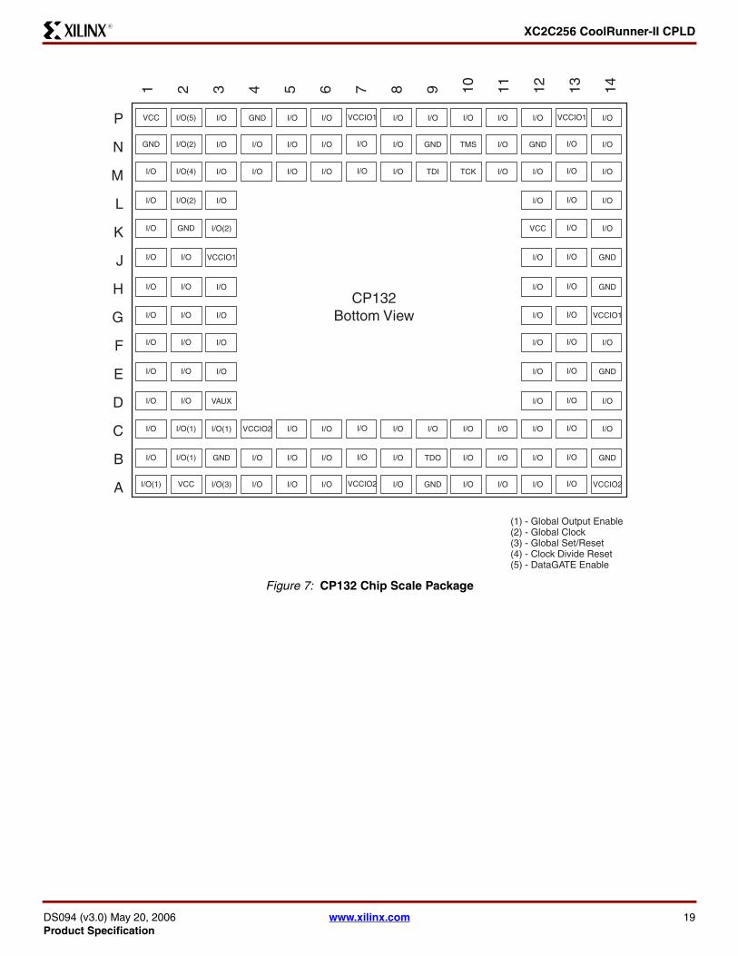
XC2C256 CoolRunner-II CPLDR
Figure 7 CP132 Chip Scale Package
CP132Bottom View
P
N
M
L
K
J
H
G
F
E
D
C
B
A
1 2 3 4 5 6 7 8 9 10 11 12 13 14
VCC VCCIO1 VCCIO1GNDIO IO IO IO IO IO IO IO IOIO(5)
IO IOVAUX IO IOIO
IO IOIO IO IOIO
IO IOIO IO VCCIO1IO
IO IOIO IO GNDIO
IO IOIO IO GNDIO
IO IOVCCIO1 IO GNDIO
IO IOIO(2) VCC IOGND
IO IOIO IO IOIO(2)
IO(1) VCCIO2 IOIOIO(3) IO IO IO GND IO IO IO VCCIO2VCC
IO IO IOIOGND IO IO IO TDO IO IO IO GNDIO(1)
IO IO IOVCCIO2IO(1) IO IO IO IO IO IO IO IOIO(1)
IO IO IOIOIO IO IO IO TDI TCK IO IO IOIO(4)
GND IO IOIOIO IO IO IO GND TMS IO GND IOIO(2)
(1) - Global Output Enable(2) - Global Clock(3) - Global SetReset(4) - Clock Divide Reset(5) - DataGATE Enable
DS094 (v30) May 20 2006 wwwxilinxcom 19Product Specification
XC2C256 CoolRunner-II CPLDR
Figure 8 TQ144 Thin Quad Flat Pack
VCCIO(1)
IO(1)
IOIO(1)
IO(1)
IOVAUX
IOIOIOIOIOIOIOIOIOIOIOIOIOIOIOIOIOIO
VCCIO1IO
GNDIO(2)
IOIO(2)
IOIO
IO(4)
GND
123456789101112131415161718192021222324252627282930313233343536
TQ144Top View
VC
CIO
(2)
IO(5
)
IO IO IO IO IO IO IOG
ND
IO IO IO IO IO IO IOV
CC
IO1
IO IO IO IO IO IOG
ND
TD
IIO
TM
SIO
TC
KIO IO IO IO
GN
D
108107106105104103102101100999897969594939291908988878685848382818079787776757473
37 38 39 40 41 42 43 44 45 46 47 48 49 50 51 52 53 54 55 56 57 58 59 60 61 62 63 64 65 66 67 68 69 70 71 72
144
143
142
141
140
139
138
137
136
135
134
133
132
131
130
129
128
127
126
125
124
123
122
121
120
119
118
117
116
115
114
113
112
111
110
109
GNDIOIOIOIOIOIOIOIOGNDIOIOIOIOIOVCCIO1IOIOGNDGNDIOIOIOIOVCCIOIOIOIOIOIOIOIOIOIOVCCIO1
GN
DIO
(3)
IO VC
CIO
2IO IO IO IO IO IO IO IO IO IO IO IO IO V
CC
IO2
IO IO IO GN
DT
DO
IO IO IO IO IO IO IO IO IO IO IO IO VC
CIO
2
(1) - Global Output Enable(2) - Global Clock(3) - Global SetReset(4) - Clock Divide Reset(5) - DataGATE Enable
20 wwwxilinxcom DS094 (v30) May 20 2006Product Specification
XC2C256 CoolRunner-II CPLDR
Figure 9 PQ208 Quad Flat Package
VCCIO
IO(1)IO
IO(1)IO
IO(1)IO
IO(1)IO
VAUXIO
GNDIOIOIOIOIOIOIOIOIOIO
GNDIO
VCCIO2IOIOIOIOIOIO
VCCIO1IOIOIOIOIOIOIOIO
GNDIO
IO(2)IO
IO(2)IOIOIOIO
IO(4)GND
PQ208Top View
VC
CI
OI
O(2
)I
OI
OI
O(5
)V
CC
IO1
IO
IO
IO
IO
IO
IO
IO
IO
GN
DI
OI
OI
OI
OI
OI
OI
OI
OI
OI
OV
CC
IO1
IO
GN
DI
OI
OI
OI
OI
OI
OI
OI
OI
OI
OV
CC
IO1
GN
DT
DI
IO
TM
SI
OT
CK
IO
IO
IO
IO
IO
GN
D
(1) - Global Output Enable(2) - Global Clock(3) - Global SetReset(4) - Clock Divide Reset(5) - DataGATE Enable
GNDIOIOIOIOIOIOIOIOIOIOIOIOIOIOGNDIOIOIOIOIOIOIOVCCIO2VCCIO1IOGNDGNDIOIOIOIOVCCIOIOIOIOIOIOIOIOIOIOIOIOIOIOIOIOIOIOVCCIO1
IO GN
DIO
(3)
IO VC
CIO
2IO IO IO IO IO IO IO IO IO IO IO IO IO G
ND
IO IO IO IO IO IO IO IO VC
CIO
2IO IO IO G
ND
TD
OIO IO IO V
CC
IO2
IO IO IO IO IO IO IO IO IO IO IO IO IO IO VC
CIO
2
12345678910111213141516171819202122232425262728293031323334353637383940414243444546474849505152
53 54 55 56 57 58 59 60 61 62 63 64 65 66 67 68 69 70 71 72 73 74 75 76 77 78 79 80 81 82 83 84 85 86 87 88 89 90 91 92 93 94 95 96 97 98 99 100
101
102
103
104
156155154153152151150149148147146145144143142141140139138137136135134133132131130129128127126125124123122121120119118117116115114113112111110109108107106105
208
207
206
205
204
203
202
201
200
199
198
197
196
195
194
193
192
191
190
189
188
187
186
185
184
183
182
181
180
179
178
177
176
175
174
173
172
171
170
169
168
167
166
165
164
163
162
161
160
159
158
157
DS094 (v30) May 20 2006 wwwxilinxcom 21Product Specification
XC2C256 CoolRunner-II CPLDR
Warranty DisclaimerTHESE PRODUCTS ARE SUBJECT TO THE TERMS OF THE XILINX LIMITED WARRANTY WHICH CAN BE VIEWEDAT httpwwwxilinxcomwarrantyhtm THIS LIMITED WARRANTY DOES NOT EXTEND TO ANY USE OF THEPRODUCTS IN AN APPLICATION OR ENVIRONMENT THAT IS NOT WITHIN THE SPECIFICATIONS STATED ON THETHEN-CURRENT XILINX DATA SHEET FOR THE PRODUCTS PRODUCTS ARE NOT DESIGNED TO BE FAIL-SAFEAND ARE NOT WARRANTED FOR USE IN APPLICATIONS THAT POSE A RISK OF PHYSICAL HARM OR LOSS OFLIFE USE OF PRODUCTS IN SUCH APPLICATIONS IS FULLY AT THE RISK OF CUSTOMER SUBJECT TOAPPLICABLE LAWS AND REGULATIONS
Figure 10 FT256 Fine Pitch Thin BGA
FT256 Bottom View
A
B
C
D
E
F
G
H
J
K
L
M
N
P
R
T
16 15 14 13 12 11 10 9 8 7 6 5 4 3 2 1
IO TDO IOIOIO IO IO IO IO IO IO IO IO IO NCIO
IO IO IOIOIO IO IO IO IO IO IO IO IO IO IOIO
IO IO IO(3)IOIO IO IO IO IO IO NC NC IO NC IONC
NC IO IO(1)IONC VCC IO IO IO IO NC VCC IO(1) IO NCIO
IO IO IOIOIO IO IO IO IO NC NC IO(1) IO(1) IO NCIO
IO VCCIO2 VAUXIOIO IO GND VCCIO2 VCCIO2 VCCIO2 GND IO IO IO NCIO
IO GND IOIOIO NC IO GND GND GND VCCIO2 IO IO NC NCIO
IO GND IOIOIO IO VCCIO2 GND GND GND VCCIO2 IO IO IO IOIO
NC GND IOIOIO IO VCCIO1 GND GND GND VCCIO1 IO IO IO IOIO
IO GND IOVCCIO NC VCCIO1 GND GND GND VCCIO1 IO IO IO IOIO
IO VCCIO1 IOIOIO IO GND VCCIO1 VCCIO1 VCCIO1 GND IO IO IO IOIO
IO NC NCIOIO IO IO NC IO IO IO IO IO(2) IO(2) IOIO
IO IO IOIOIO TMS IO IO IO IO IO IO IO IO IOIO
IO IO IOIOIO TCK NC NC IO IO IO IO(2) VCC IO(4) IOIO
IO IO IOIOIO IO TDI IO IO IO IO IO IO IO IOIO
IO IO IONCNC NC NC NC IO IO IO IO IO IO(5) IOIO
(1) - Global Output Enable(2) - Global Clock(3) - Global SetReset(4) - Clock Divide Reset(5) - DataGATE Enable
22 wwwxilinxcom DS094 (v30) May 20 2006Product Specification
XC2C256 CoolRunner-II CPLDR
Additional InformationAdditional information is available for the following CoolRunner-II topics
bull XAPP784 Bulletproof CPLD Design Practicesbull XAPP375 Timing Model bull XAPP376 Logic Engine bull XAPP378 Advanced Features bull XAPP382 IO Characteristics bull XAPP389 Powering CoolRunner-II bull XAPP399 Assigning VREF Pins
To access these and all application notes with their associ-ated reference designs click the following link and scrolldown the page until you find the document you want
CoolRunner-II Data Sheets and Application Notes
Device Packages
Revision HistoryThe following table shows the revision history for this document
Date Version Revision
050902 10 Initial Xilinx release
051302 11 Updated AC Electrical Characteristics and added new parameters
103102 12 Corrected package user IO added Voltage Referenced DC tables
031703 20 Added Characterization numbers for product release and device part marking
040203 21 Updated TSOL max from 260 to 220 Changed ICCSB units from mA to μA
012604 22 Updated Device Part Marking Updated links and Tsol
022604 23 Corrected Theta JC value on XC2C256-7TQ144
080304 24 Pb-free documentation
081904 25 Changes to ICCSB maximum specifications in DC Electrical Characteristics table on page 3
100104 26 Add Asynchronous PresetReset Pulse Width specification to AC Electrical Characteristics
030705 27 Removed -5 speed grade Changes to Table 1 IO Standards
062805 28 Move to Product Specification Change to TIN25 TOUT25 TIN33 and TOUT33 for -7 speed grade
032006 29 Add Warranty Disclaimer Add note to Pin Description table that GTS GSR and GCK pins can be used for general purpose IO
52006 30 Moved TCONFIG specification values from MIN column to MAX column page 7
DS094 (v30) May 20 2006 wwwxilinxcom 23Product Specification
- Features
- Description
- RealDigital Design Technology
- Supported IO Standards
- Absolute Maximum Ratings
- Recommended Operating Conditions
- DC Electrical Characteristics (Over Recommended Operating Conditions)
- LVCMOS 33V and LVTTL 33V DC Voltage Specifications
- LVCMOS 25V DC Voltage Specifications
- LVCMOS 18V DC Voltage Specifications
- LVCMOS 15V DC Voltage Specifications(1)
- Schmitt Trigger Input DC Voltage Specifications
- SSTL2-1 DC Voltage Specifications
- SSTL3-1 DC Voltage Specifications
- HSTL1 DC Voltage Specifications
- AC Electrical Characteristics Over Recommended Operating Conditions
- Internal Timing Parameters
-
- Switching Characteristics
- AC Test Circuit
-
- Pin Descriptions
-
- XC2C256 JTAG PowerGround No Connect Pins and Total User IO
-
- Warranty Disclaimer
- Additional Information
- Revision History
-
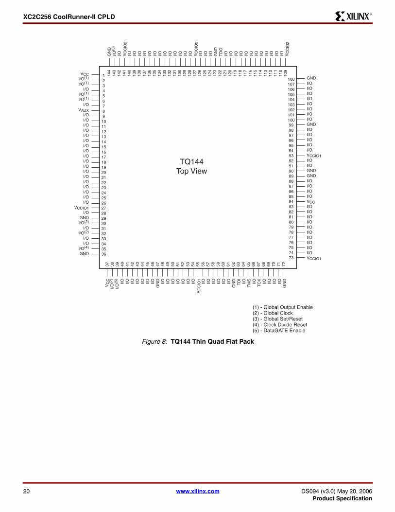
XC2C256 CoolRunner-II CPLDR
Figure 8 TQ144 Thin Quad Flat Pack
VCCIO(1)
IO(1)
IOIO(1)
IO(1)
IOVAUX
IOIOIOIOIOIOIOIOIOIOIOIOIOIOIOIOIOIO
VCCIO1IO
GNDIO(2)
IOIO(2)
IOIO
IO(4)
GND
123456789101112131415161718192021222324252627282930313233343536
TQ144Top View
VC
CIO
(2)
IO(5
)
IO IO IO IO IO IO IOG
ND
IO IO IO IO IO IO IOV
CC
IO1
IO IO IO IO IO IOG
ND
TD
IIO
TM
SIO
TC
KIO IO IO IO
GN
D
108107106105104103102101100999897969594939291908988878685848382818079787776757473
37 38 39 40 41 42 43 44 45 46 47 48 49 50 51 52 53 54 55 56 57 58 59 60 61 62 63 64 65 66 67 68 69 70 71 72
144
143
142
141
140
139
138
137
136
135
134
133
132
131
130
129
128
127
126
125
124
123
122
121
120
119
118
117
116
115
114
113
112
111
110
109
GNDIOIOIOIOIOIOIOIOGNDIOIOIOIOIOVCCIO1IOIOGNDGNDIOIOIOIOVCCIOIOIOIOIOIOIOIOIOIOVCCIO1
GN
DIO
(3)
IO VC
CIO
2IO IO IO IO IO IO IO IO IO IO IO IO IO V
CC
IO2
IO IO IO GN
DT
DO
IO IO IO IO IO IO IO IO IO IO IO IO VC
CIO
2
(1) - Global Output Enable(2) - Global Clock(3) - Global SetReset(4) - Clock Divide Reset(5) - DataGATE Enable
20 wwwxilinxcom DS094 (v30) May 20 2006Product Specification
XC2C256 CoolRunner-II CPLDR
Figure 9 PQ208 Quad Flat Package
VCCIO
IO(1)IO
IO(1)IO
IO(1)IO
IO(1)IO
VAUXIO
GNDIOIOIOIOIOIOIOIOIOIO
GNDIO
VCCIO2IOIOIOIOIOIO
VCCIO1IOIOIOIOIOIOIOIO
GNDIO
IO(2)IO
IO(2)IOIOIOIO
IO(4)GND
PQ208Top View
VC
CI
OI
O(2
)I
OI
OI
O(5
)V
CC
IO1
IO
IO
IO
IO
IO
IO
IO
IO
GN
DI
OI
OI
OI
OI
OI
OI
OI
OI
OI
OV
CC
IO1
IO
GN
DI
OI
OI
OI
OI
OI
OI
OI
OI
OI
OV
CC
IO1
GN
DT
DI
IO
TM
SI
OT
CK
IO
IO
IO
IO
IO
GN
D
(1) - Global Output Enable(2) - Global Clock(3) - Global SetReset(4) - Clock Divide Reset(5) - DataGATE Enable
GNDIOIOIOIOIOIOIOIOIOIOIOIOIOIOGNDIOIOIOIOIOIOIOVCCIO2VCCIO1IOGNDGNDIOIOIOIOVCCIOIOIOIOIOIOIOIOIOIOIOIOIOIOIOIOIOIOVCCIO1
IO GN
DIO
(3)
IO VC
CIO
2IO IO IO IO IO IO IO IO IO IO IO IO IO G
ND
IO IO IO IO IO IO IO IO VC
CIO
2IO IO IO G
ND
TD
OIO IO IO V
CC
IO2
IO IO IO IO IO IO IO IO IO IO IO IO IO IO VC
CIO
2
12345678910111213141516171819202122232425262728293031323334353637383940414243444546474849505152
53 54 55 56 57 58 59 60 61 62 63 64 65 66 67 68 69 70 71 72 73 74 75 76 77 78 79 80 81 82 83 84 85 86 87 88 89 90 91 92 93 94 95 96 97 98 99 100
101
102
103
104
156155154153152151150149148147146145144143142141140139138137136135134133132131130129128127126125124123122121120119118117116115114113112111110109108107106105
208
207
206
205
204
203
202
201
200
199
198
197
196
195
194
193
192
191
190
189
188
187
186
185
184
183
182
181
180
179
178
177
176
175
174
173
172
171
170
169
168
167
166
165
164
163
162
161
160
159
158
157
DS094 (v30) May 20 2006 wwwxilinxcom 21Product Specification
XC2C256 CoolRunner-II CPLDR
Warranty DisclaimerTHESE PRODUCTS ARE SUBJECT TO THE TERMS OF THE XILINX LIMITED WARRANTY WHICH CAN BE VIEWEDAT httpwwwxilinxcomwarrantyhtm THIS LIMITED WARRANTY DOES NOT EXTEND TO ANY USE OF THEPRODUCTS IN AN APPLICATION OR ENVIRONMENT THAT IS NOT WITHIN THE SPECIFICATIONS STATED ON THETHEN-CURRENT XILINX DATA SHEET FOR THE PRODUCTS PRODUCTS ARE NOT DESIGNED TO BE FAIL-SAFEAND ARE NOT WARRANTED FOR USE IN APPLICATIONS THAT POSE A RISK OF PHYSICAL HARM OR LOSS OFLIFE USE OF PRODUCTS IN SUCH APPLICATIONS IS FULLY AT THE RISK OF CUSTOMER SUBJECT TOAPPLICABLE LAWS AND REGULATIONS
Figure 10 FT256 Fine Pitch Thin BGA
FT256 Bottom View
A
B
C
D
E
F
G
H
J
K
L
M
N
P
R
T
16 15 14 13 12 11 10 9 8 7 6 5 4 3 2 1
IO TDO IOIOIO IO IO IO IO IO IO IO IO IO NCIO
IO IO IOIOIO IO IO IO IO IO IO IO IO IO IOIO
IO IO IO(3)IOIO IO IO IO IO IO NC NC IO NC IONC
NC IO IO(1)IONC VCC IO IO IO IO NC VCC IO(1) IO NCIO
IO IO IOIOIO IO IO IO IO NC NC IO(1) IO(1) IO NCIO
IO VCCIO2 VAUXIOIO IO GND VCCIO2 VCCIO2 VCCIO2 GND IO IO IO NCIO
IO GND IOIOIO NC IO GND GND GND VCCIO2 IO IO NC NCIO
IO GND IOIOIO IO VCCIO2 GND GND GND VCCIO2 IO IO IO IOIO
NC GND IOIOIO IO VCCIO1 GND GND GND VCCIO1 IO IO IO IOIO
IO GND IOVCCIO NC VCCIO1 GND GND GND VCCIO1 IO IO IO IOIO
IO VCCIO1 IOIOIO IO GND VCCIO1 VCCIO1 VCCIO1 GND IO IO IO IOIO
IO NC NCIOIO IO IO NC IO IO IO IO IO(2) IO(2) IOIO
IO IO IOIOIO TMS IO IO IO IO IO IO IO IO IOIO
IO IO IOIOIO TCK NC NC IO IO IO IO(2) VCC IO(4) IOIO
IO IO IOIOIO IO TDI IO IO IO IO IO IO IO IOIO
IO IO IONCNC NC NC NC IO IO IO IO IO IO(5) IOIO
(1) - Global Output Enable(2) - Global Clock(3) - Global SetReset(4) - Clock Divide Reset(5) - DataGATE Enable
22 wwwxilinxcom DS094 (v30) May 20 2006Product Specification
XC2C256 CoolRunner-II CPLDR
Additional InformationAdditional information is available for the following CoolRunner-II topics
bull XAPP784 Bulletproof CPLD Design Practicesbull XAPP375 Timing Model bull XAPP376 Logic Engine bull XAPP378 Advanced Features bull XAPP382 IO Characteristics bull XAPP389 Powering CoolRunner-II bull XAPP399 Assigning VREF Pins
To access these and all application notes with their associ-ated reference designs click the following link and scrolldown the page until you find the document you want
CoolRunner-II Data Sheets and Application Notes
Device Packages
Revision HistoryThe following table shows the revision history for this document
Date Version Revision
050902 10 Initial Xilinx release
051302 11 Updated AC Electrical Characteristics and added new parameters
103102 12 Corrected package user IO added Voltage Referenced DC tables
031703 20 Added Characterization numbers for product release and device part marking
040203 21 Updated TSOL max from 260 to 220 Changed ICCSB units from mA to μA
012604 22 Updated Device Part Marking Updated links and Tsol
022604 23 Corrected Theta JC value on XC2C256-7TQ144
080304 24 Pb-free documentation
081904 25 Changes to ICCSB maximum specifications in DC Electrical Characteristics table on page 3
100104 26 Add Asynchronous PresetReset Pulse Width specification to AC Electrical Characteristics
030705 27 Removed -5 speed grade Changes to Table 1 IO Standards
062805 28 Move to Product Specification Change to TIN25 TOUT25 TIN33 and TOUT33 for -7 speed grade
032006 29 Add Warranty Disclaimer Add note to Pin Description table that GTS GSR and GCK pins can be used for general purpose IO
52006 30 Moved TCONFIG specification values from MIN column to MAX column page 7
DS094 (v30) May 20 2006 wwwxilinxcom 23Product Specification
- Features
- Description
- RealDigital Design Technology
- Supported IO Standards
- Absolute Maximum Ratings
- Recommended Operating Conditions
- DC Electrical Characteristics (Over Recommended Operating Conditions)
- LVCMOS 33V and LVTTL 33V DC Voltage Specifications
- LVCMOS 25V DC Voltage Specifications
- LVCMOS 18V DC Voltage Specifications
- LVCMOS 15V DC Voltage Specifications(1)
- Schmitt Trigger Input DC Voltage Specifications
- SSTL2-1 DC Voltage Specifications
- SSTL3-1 DC Voltage Specifications
- HSTL1 DC Voltage Specifications
- AC Electrical Characteristics Over Recommended Operating Conditions
- Internal Timing Parameters
-
- Switching Characteristics
- AC Test Circuit
-
- Pin Descriptions
-
- XC2C256 JTAG PowerGround No Connect Pins and Total User IO
-
- Warranty Disclaimer
- Additional Information
- Revision History
-
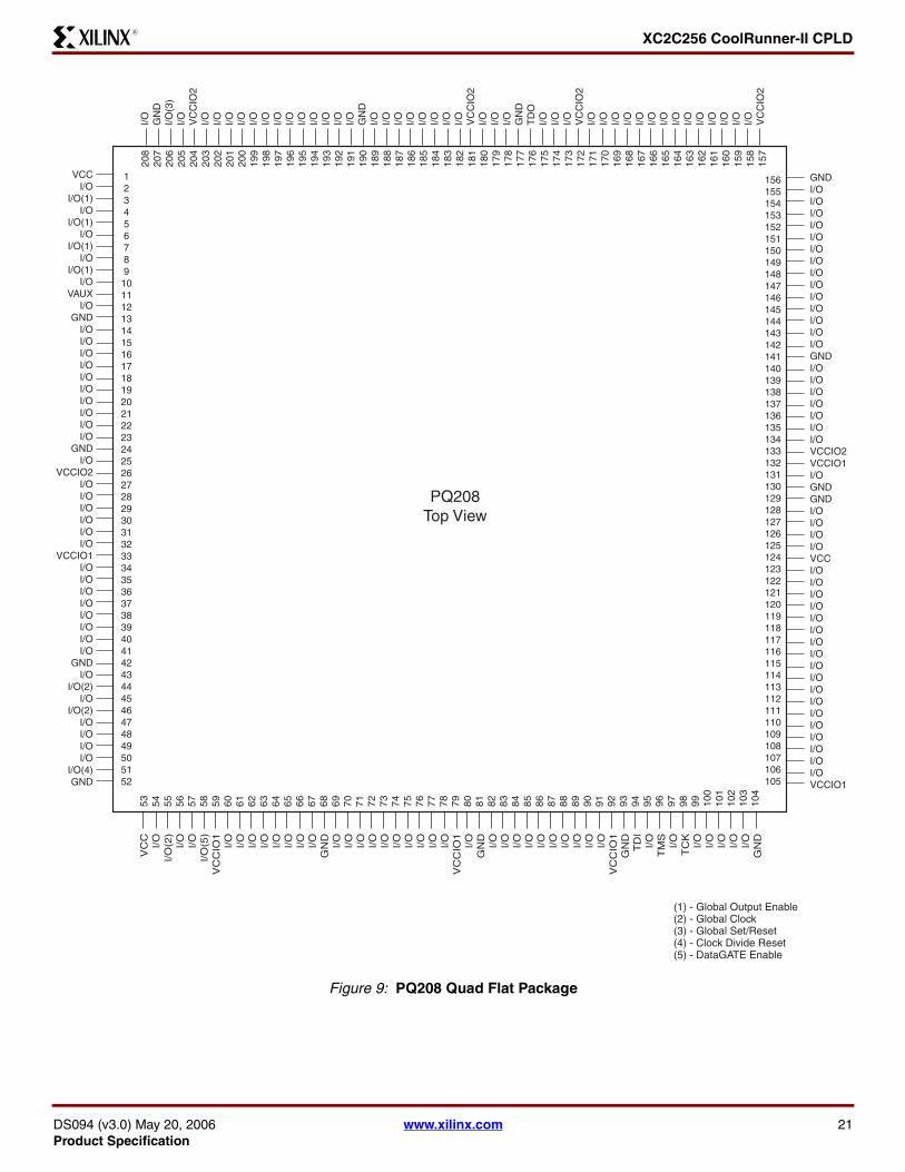
XC2C256 CoolRunner-II CPLDR
Figure 9 PQ208 Quad Flat Package
VCCIO
IO(1)IO
IO(1)IO
IO(1)IO
IO(1)IO
VAUXIO
GNDIOIOIOIOIOIOIOIOIOIO
GNDIO
VCCIO2IOIOIOIOIOIO
VCCIO1IOIOIOIOIOIOIOIO
GNDIO
IO(2)IO
IO(2)IOIOIOIO
IO(4)GND
PQ208Top View
VC
CI
OI
O(2
)I
OI
OI
O(5
)V
CC
IO1
IO
IO
IO
IO
IO
IO
IO
IO
GN
DI
OI
OI
OI
OI
OI
OI
OI
OI
OI
OV
CC
IO1
IO
GN
DI
OI
OI
OI
OI
OI
OI
OI
OI
OI
OV
CC
IO1
GN
DT
DI
IO
TM
SI
OT
CK
IO
IO
IO
IO
IO
GN
D
(1) - Global Output Enable(2) - Global Clock(3) - Global SetReset(4) - Clock Divide Reset(5) - DataGATE Enable
GNDIOIOIOIOIOIOIOIOIOIOIOIOIOIOGNDIOIOIOIOIOIOIOVCCIO2VCCIO1IOGNDGNDIOIOIOIOVCCIOIOIOIOIOIOIOIOIOIOIOIOIOIOIOIOIOIOVCCIO1
IO GN
DIO
(3)
IO VC
CIO
2IO IO IO IO IO IO IO IO IO IO IO IO IO G
ND
IO IO IO IO IO IO IO IO VC
CIO
2IO IO IO G
ND
TD
OIO IO IO V
CC
IO2
IO IO IO IO IO IO IO IO IO IO IO IO IO IO VC
CIO
2
12345678910111213141516171819202122232425262728293031323334353637383940414243444546474849505152
53 54 55 56 57 58 59 60 61 62 63 64 65 66 67 68 69 70 71 72 73 74 75 76 77 78 79 80 81 82 83 84 85 86 87 88 89 90 91 92 93 94 95 96 97 98 99 100
101
102
103
104
156155154153152151150149148147146145144143142141140139138137136135134133132131130129128127126125124123122121120119118117116115114113112111110109108107106105
208
207
206
205
204
203
202
201
200
199
198
197
196
195
194
193
192
191
190
189
188
187
186
185
184
183
182
181
180
179
178
177
176
175
174
173
172
171
170
169
168
167
166
165
164
163
162
161
160
159
158
157
DS094 (v30) May 20 2006 wwwxilinxcom 21Product Specification
XC2C256 CoolRunner-II CPLDR
Warranty DisclaimerTHESE PRODUCTS ARE SUBJECT TO THE TERMS OF THE XILINX LIMITED WARRANTY WHICH CAN BE VIEWEDAT httpwwwxilinxcomwarrantyhtm THIS LIMITED WARRANTY DOES NOT EXTEND TO ANY USE OF THEPRODUCTS IN AN APPLICATION OR ENVIRONMENT THAT IS NOT WITHIN THE SPECIFICATIONS STATED ON THETHEN-CURRENT XILINX DATA SHEET FOR THE PRODUCTS PRODUCTS ARE NOT DESIGNED TO BE FAIL-SAFEAND ARE NOT WARRANTED FOR USE IN APPLICATIONS THAT POSE A RISK OF PHYSICAL HARM OR LOSS OFLIFE USE OF PRODUCTS IN SUCH APPLICATIONS IS FULLY AT THE RISK OF CUSTOMER SUBJECT TOAPPLICABLE LAWS AND REGULATIONS
Figure 10 FT256 Fine Pitch Thin BGA
FT256 Bottom View
A
B
C
D
E
F
G
H
J
K
L
M
N
P
R
T
16 15 14 13 12 11 10 9 8 7 6 5 4 3 2 1
IO TDO IOIOIO IO IO IO IO IO IO IO IO IO NCIO
IO IO IOIOIO IO IO IO IO IO IO IO IO IO IOIO
IO IO IO(3)IOIO IO IO IO IO IO NC NC IO NC IONC
NC IO IO(1)IONC VCC IO IO IO IO NC VCC IO(1) IO NCIO
IO IO IOIOIO IO IO IO IO NC NC IO(1) IO(1) IO NCIO
IO VCCIO2 VAUXIOIO IO GND VCCIO2 VCCIO2 VCCIO2 GND IO IO IO NCIO
IO GND IOIOIO NC IO GND GND GND VCCIO2 IO IO NC NCIO
IO GND IOIOIO IO VCCIO2 GND GND GND VCCIO2 IO IO IO IOIO
NC GND IOIOIO IO VCCIO1 GND GND GND VCCIO1 IO IO IO IOIO
IO GND IOVCCIO NC VCCIO1 GND GND GND VCCIO1 IO IO IO IOIO
IO VCCIO1 IOIOIO IO GND VCCIO1 VCCIO1 VCCIO1 GND IO IO IO IOIO
IO NC NCIOIO IO IO NC IO IO IO IO IO(2) IO(2) IOIO
IO IO IOIOIO TMS IO IO IO IO IO IO IO IO IOIO
IO IO IOIOIO TCK NC NC IO IO IO IO(2) VCC IO(4) IOIO
IO IO IOIOIO IO TDI IO IO IO IO IO IO IO IOIO
IO IO IONCNC NC NC NC IO IO IO IO IO IO(5) IOIO
(1) - Global Output Enable(2) - Global Clock(3) - Global SetReset(4) - Clock Divide Reset(5) - DataGATE Enable
22 wwwxilinxcom DS094 (v30) May 20 2006Product Specification
XC2C256 CoolRunner-II CPLDR
Additional InformationAdditional information is available for the following CoolRunner-II topics
bull XAPP784 Bulletproof CPLD Design Practicesbull XAPP375 Timing Model bull XAPP376 Logic Engine bull XAPP378 Advanced Features bull XAPP382 IO Characteristics bull XAPP389 Powering CoolRunner-II bull XAPP399 Assigning VREF Pins
To access these and all application notes with their associ-ated reference designs click the following link and scrolldown the page until you find the document you want
CoolRunner-II Data Sheets and Application Notes
Device Packages
Revision HistoryThe following table shows the revision history for this document
Date Version Revision
050902 10 Initial Xilinx release
051302 11 Updated AC Electrical Characteristics and added new parameters
103102 12 Corrected package user IO added Voltage Referenced DC tables
031703 20 Added Characterization numbers for product release and device part marking
040203 21 Updated TSOL max from 260 to 220 Changed ICCSB units from mA to μA
012604 22 Updated Device Part Marking Updated links and Tsol
022604 23 Corrected Theta JC value on XC2C256-7TQ144
080304 24 Pb-free documentation
081904 25 Changes to ICCSB maximum specifications in DC Electrical Characteristics table on page 3
100104 26 Add Asynchronous PresetReset Pulse Width specification to AC Electrical Characteristics
030705 27 Removed -5 speed grade Changes to Table 1 IO Standards
062805 28 Move to Product Specification Change to TIN25 TOUT25 TIN33 and TOUT33 for -7 speed grade
032006 29 Add Warranty Disclaimer Add note to Pin Description table that GTS GSR and GCK pins can be used for general purpose IO
52006 30 Moved TCONFIG specification values from MIN column to MAX column page 7
DS094 (v30) May 20 2006 wwwxilinxcom 23Product Specification
- Features
- Description
- RealDigital Design Technology
- Supported IO Standards
- Absolute Maximum Ratings
- Recommended Operating Conditions
- DC Electrical Characteristics (Over Recommended Operating Conditions)
- LVCMOS 33V and LVTTL 33V DC Voltage Specifications
- LVCMOS 25V DC Voltage Specifications
- LVCMOS 18V DC Voltage Specifications
- LVCMOS 15V DC Voltage Specifications(1)
- Schmitt Trigger Input DC Voltage Specifications
- SSTL2-1 DC Voltage Specifications
- SSTL3-1 DC Voltage Specifications
- HSTL1 DC Voltage Specifications
- AC Electrical Characteristics Over Recommended Operating Conditions
- Internal Timing Parameters
-
- Switching Characteristics
- AC Test Circuit
-
- Pin Descriptions
-
- XC2C256 JTAG PowerGround No Connect Pins and Total User IO
-
- Warranty Disclaimer
- Additional Information
- Revision History
-
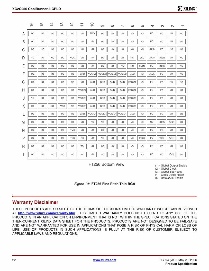
XC2C256 CoolRunner-II CPLDR
Warranty DisclaimerTHESE PRODUCTS ARE SUBJECT TO THE TERMS OF THE XILINX LIMITED WARRANTY WHICH CAN BE VIEWEDAT httpwwwxilinxcomwarrantyhtm THIS LIMITED WARRANTY DOES NOT EXTEND TO ANY USE OF THEPRODUCTS IN AN APPLICATION OR ENVIRONMENT THAT IS NOT WITHIN THE SPECIFICATIONS STATED ON THETHEN-CURRENT XILINX DATA SHEET FOR THE PRODUCTS PRODUCTS ARE NOT DESIGNED TO BE FAIL-SAFEAND ARE NOT WARRANTED FOR USE IN APPLICATIONS THAT POSE A RISK OF PHYSICAL HARM OR LOSS OFLIFE USE OF PRODUCTS IN SUCH APPLICATIONS IS FULLY AT THE RISK OF CUSTOMER SUBJECT TOAPPLICABLE LAWS AND REGULATIONS
Figure 10 FT256 Fine Pitch Thin BGA
FT256 Bottom View
A
B
C
D
E
F
G
H
J
K
L
M
N
P
R
T
16 15 14 13 12 11 10 9 8 7 6 5 4 3 2 1
IO TDO IOIOIO IO IO IO IO IO IO IO IO IO NCIO
IO IO IOIOIO IO IO IO IO IO IO IO IO IO IOIO
IO IO IO(3)IOIO IO IO IO IO IO NC NC IO NC IONC
NC IO IO(1)IONC VCC IO IO IO IO NC VCC IO(1) IO NCIO
IO IO IOIOIO IO IO IO IO NC NC IO(1) IO(1) IO NCIO
IO VCCIO2 VAUXIOIO IO GND VCCIO2 VCCIO2 VCCIO2 GND IO IO IO NCIO
IO GND IOIOIO NC IO GND GND GND VCCIO2 IO IO NC NCIO
IO GND IOIOIO IO VCCIO2 GND GND GND VCCIO2 IO IO IO IOIO
NC GND IOIOIO IO VCCIO1 GND GND GND VCCIO1 IO IO IO IOIO
IO GND IOVCCIO NC VCCIO1 GND GND GND VCCIO1 IO IO IO IOIO
IO VCCIO1 IOIOIO IO GND VCCIO1 VCCIO1 VCCIO1 GND IO IO IO IOIO
IO NC NCIOIO IO IO NC IO IO IO IO IO(2) IO(2) IOIO
IO IO IOIOIO TMS IO IO IO IO IO IO IO IO IOIO
IO IO IOIOIO TCK NC NC IO IO IO IO(2) VCC IO(4) IOIO
IO IO IOIOIO IO TDI IO IO IO IO IO IO IO IOIO
IO IO IONCNC NC NC NC IO IO IO IO IO IO(5) IOIO
(1) - Global Output Enable(2) - Global Clock(3) - Global SetReset(4) - Clock Divide Reset(5) - DataGATE Enable
22 wwwxilinxcom DS094 (v30) May 20 2006Product Specification
XC2C256 CoolRunner-II CPLDR
Additional InformationAdditional information is available for the following CoolRunner-II topics
bull XAPP784 Bulletproof CPLD Design Practicesbull XAPP375 Timing Model bull XAPP376 Logic Engine bull XAPP378 Advanced Features bull XAPP382 IO Characteristics bull XAPP389 Powering CoolRunner-II bull XAPP399 Assigning VREF Pins
To access these and all application notes with their associ-ated reference designs click the following link and scrolldown the page until you find the document you want
CoolRunner-II Data Sheets and Application Notes
Device Packages
Revision HistoryThe following table shows the revision history for this document
Date Version Revision
050902 10 Initial Xilinx release
051302 11 Updated AC Electrical Characteristics and added new parameters
103102 12 Corrected package user IO added Voltage Referenced DC tables
031703 20 Added Characterization numbers for product release and device part marking
040203 21 Updated TSOL max from 260 to 220 Changed ICCSB units from mA to μA
012604 22 Updated Device Part Marking Updated links and Tsol
022604 23 Corrected Theta JC value on XC2C256-7TQ144
080304 24 Pb-free documentation
081904 25 Changes to ICCSB maximum specifications in DC Electrical Characteristics table on page 3
100104 26 Add Asynchronous PresetReset Pulse Width specification to AC Electrical Characteristics
030705 27 Removed -5 speed grade Changes to Table 1 IO Standards
062805 28 Move to Product Specification Change to TIN25 TOUT25 TIN33 and TOUT33 for -7 speed grade
032006 29 Add Warranty Disclaimer Add note to Pin Description table that GTS GSR and GCK pins can be used for general purpose IO
52006 30 Moved TCONFIG specification values from MIN column to MAX column page 7
DS094 (v30) May 20 2006 wwwxilinxcom 23Product Specification
- Features
- Description
- RealDigital Design Technology
- Supported IO Standards
- Absolute Maximum Ratings
- Recommended Operating Conditions
- DC Electrical Characteristics (Over Recommended Operating Conditions)
- LVCMOS 33V and LVTTL 33V DC Voltage Specifications
- LVCMOS 25V DC Voltage Specifications
- LVCMOS 18V DC Voltage Specifications
- LVCMOS 15V DC Voltage Specifications(1)
- Schmitt Trigger Input DC Voltage Specifications
- SSTL2-1 DC Voltage Specifications
- SSTL3-1 DC Voltage Specifications
- HSTL1 DC Voltage Specifications
- AC Electrical Characteristics Over Recommended Operating Conditions
- Internal Timing Parameters
-
- Switching Characteristics
- AC Test Circuit
-
- Pin Descriptions
-
- XC2C256 JTAG PowerGround No Connect Pins and Total User IO
-
- Warranty Disclaimer
- Additional Information
- Revision History
-
Related Documents