XAPP1183 (v1.0) November 18, 2013 www.xilinx.com 1 © Copyright 2013 Xilinx, Inc. Xilinx, the Xilinx logo, Artix, ISE, Kintex, Spartan, Virtex, Vivado, Zynq, and other designated brands included herein are trademarks of Xilinx in the United States and other countries. All other trademarks are the property of their respective owners. Summary This application note describes how the Xilinx analog-to-digital converter (XADC) acquires analog data using its dedicated Vp/Vn analog input. The design implements a use case where the XADC out data is transferred directly to system memory using the Xilinx direct memory access (DMA) IP. A Linux-based application running on a Zynq®-7000 All Programmable (AP) SoC processing system (PS) reads the buffer from memory, and a LabView-based application GUI gathers the data and performs fast fourier transform (FFT) processing on the data to quantify the signal-to-noise ratio (SNR) of the XADC out data. Introduction The Zynq-7000 family is based on the Xilinx AP SoC architecture. These products integrate a feature-rich dual-core ARM® Cortex™-A9 based processing system and 28 nm Xilinx programmable logic (PL) in a single device. The ARM Cortex-A9 CPUs are the heart of the PS and also include on-chip memory, external memory interfaces, and a rich set of peripheral connectivity interfaces. The XADC is an integrated 12-bit, 17 channel, 1 MSPS ADC. The Zynq-7000 AP SoC PS communicates with the XADC using an AXI interface when the XADC is instantiated in the PL. The XADC is an embedded block available in all Zynq-7000 AP SoCs. The LogiCORE™ XADC wizard IP provides an AXI4-Lite compatible interface and an optional AXI4-Stream interface. The AXI4-Lite interface is used to configure the XADC, and the AXI4-Stream interface is used for data communication. The AXI4-Stream interface includes options for interfacing the XADC data interface to other signal processing IP. This application note demonstrates using the AXI4-Lite interface to control the XADC configuration parameters, and using the AXI4-Stream interface to capture samples of the input analog data. This application note provides a hardware design in the PL that establishes the datapath between the XADC and the PS using the general-purpose (GP) port interface. An AXI DMA is used to interface to the XADC AXI4-Stream interface, and the DMA stores the XADC samples in the PS DDR3. The Cortex-A9 processor is used to configure the XADC for user-specific configuration parameters. A LabView based GUI interface is provided to configure the XADC and display the collected samples. The samples are analyzed in the GUI to plot the linearity of the samples and various performance characteristics of the XADC, including signal-to-noise ratio (SNR), total harmonic distortion (THD), signal-to-noise and distortion (SINAD), and effective number of bits (ENOB). The LabView GUI interfaces to the XADC with the UART interface. Application Note: Zynq-7000 Processing System XAPP1183 (v1.0) November 18, 2013 Implementing Analog Data Acquisition using the Zynq-7000 AP SoC Processing System with the XADC AXI Interface Authors: Mrinal J. Sarmah and Radhey S. Pandey

Welcome message from author
This document is posted to help you gain knowledge. Please leave a comment to let me know what you think about it! Share it to your friends and learn new things together.
Transcript
XAPP1183 (v1.0) November 18, 2013 www.xilinx.com 1
© Copyright 2013 Xilinx, Inc. Xilinx, the Xilinx logo, Artix, ISE, Kintex, Spartan, Virtex, Vivado, Zynq, and other designated brands included herein are trademarks of Xilinx in the United States and other countries. All other trademarks are the property of their respective owners.
Summary This application note describes how the Xilinx analog-to-digital converter (XADC) acquires analog data using its dedicated Vp/Vn analog input. The design implements a use case where the XADC out data is transferred directly to system memory using the Xilinx direct memory access (DMA) IP. A Linux-based application running on a Zynq®-7000 All Programmable (AP) SoC processing system (PS) reads the buffer from memory, and a LabView-based application GUI gathers the data and performs fast fourier transform (FFT) processing on the data to quantify the signal-to-noise ratio (SNR) of the XADC out data.
Introduction The Zynq-7000 family is based on the Xilinx AP SoC architecture. These products integrate a feature-rich dual-core ARM® Cortex™-A9 based processing system and 28 nm Xilinx programmable logic (PL) in a single device. The ARM Cortex-A9 CPUs are the heart of the PS and also include on-chip memory, external memory interfaces, and a rich set of peripheral connectivity interfaces.
The XADC is an integrated 12-bit, 17 channel, 1 MSPS ADC. The Zynq-7000 AP SoC PS communicates with the XADC using an AXI interface when the XADC is instantiated in the PL. The XADC is an embedded block available in all Zynq-7000 AP SoCs.
The LogiCORE™ XADC wizard IP provides an AXI4-Lite compatible interface and an optional AXI4-Stream interface. The AXI4-Lite interface is used to configure the XADC, and the AXI4-Stream interface is used for data communication. The AXI4-Stream interface includes options for interfacing the XADC data interface to other signal processing IP. This application note demonstrates using the AXI4-Lite interface to control the XADC configuration parameters, and using the AXI4-Stream interface to capture samples of the input analog data.
This application note provides a hardware design in the PL that establishes the datapath between the XADC and the PS using the general-purpose (GP) port interface. An AXI DMA is used to interface to the XADC AXI4-Stream interface, and the DMA stores the XADC samples in the PS DDR3. The Cortex-A9 processor is used to configure the XADC for user-specific configuration parameters.
A LabView based GUI interface is provided to configure the XADC and display the collected samples. The samples are analyzed in the GUI to plot the linearity of the samples and various performance characteristics of the XADC, including signal-to-noise ratio (SNR), total harmonic distortion (THD), signal-to-noise and distortion (SINAD), and effective number of bits (ENOB). The LabView GUI interfaces to the XADC with the UART interface.
Application Note: Zynq-7000 Processing System
XAPP1183 (v1.0) November 18, 2013
Implementing Analog Data Acquisition using the Zynq-7000 AP SoC Processing System with the XADC AXI InterfaceAuthors: Mrinal J. Sarmah and Radhey S. Pandey

Hardware Design Overview
XAPP1183 (v1.0) November 18, 2013 www.xilinx.com 2
Hardware Design Overview
The XADC IP uses an AXI4-Stream interface that provides XADC samples to the streaming application. The XADC samples are valid when TVALID from the interface is asserted. The hardware design coalesces 4096 XADC samples and generates the TLAST signal, which is required by the AXI DMA IP to identify the frame boundary of an AXI4-Stream transfer. The AXI DMA writes the 4096 samples back to the PS DDR3 memory and asserts an interrupt to the processor. Figure 1 shows the hardware block diagram.
The data flow sequence is:
1. The Linux driver for the XADC initializes the XADC block by setting up the sampling frequency to 961.54 kilo-samples per second (KS/S) and making the XADC work in continuous sampling mode.
2. The Linux driver sets up the XADC DMA registers, including the S2MM data and length register.
3. The XADC block captures data from an external analog source and stores it in a FIFO.
4. The FIFO adapter block generates an end of packet based on a coalesce count programmed by the DMA software. The default coalesce count is 8192 bytes of samples.
5. The FIFO adapter block's output interfaces with the DMA AXI4-Stream interface.
X-Ref Target - Figure 1
Figure 1: Hardware Block Diagram

Hardware Design Overview
XAPP1183 (v1.0) November 18, 2013 www.xilinx.com 3
6. The XADC wizard IP asserts an interrupt through the fabric-to-PS interrupt pin when the data transfer is done.
The interrupt port from the XADC wizard is connected to the Zynq-7000 PS IRQ_F2P interrupt port 0 with ID 91.
The design uses the Vivado® Design Suite IP Integrator (IPI) flow for creating the block design. Once the block design is created, a hardware wrapper is generated that instantiates the IP-specific wrapper files.
Table 1 shows the Xilinx IPs used in the hardware design.
Table 2 shows the address map of the memory mapped peripheral in the PL.
Table 1: IPs Used in the Hardware Design
IP Name Description Configuration
Processing System-7
Generates a wrapper that instantiates the Processing System-7 embedded blocks
Configured with the ZC702 default preset from the Processing System-7 IP wizard
AXI Interconnect IP
AXI Interconnect IP that converts AXI3 transactions from the Processing System-7 IP to AXI4 transactions for the XADC Wizard IP
Configured for one master and one slave interface
XADC Wizard IP
XADC Wizard IP instantiates the XADC embedded block and converts AXI4-Lite transactions to DRP transactions required by the embedded block
Configured to support AXI4-Stream Interface with built-in FIFO
Proc Sys ResetApplies reset to peripherals and AXI Interconnect IP
Configured to apply reset to AXI Interconnect and the XADC Wizard IP
AXI DMA IP
• Collects samples from the AXI4-Stream interface of the XADC Wizard IP and stores them in the DDR3 memory
• The DMA IP interfaces to a GP slave port
Configured for simple DMA mode by disabling scatter-gather operation
Table 2: Address Map of the Peripheral
Peripheral in PL Address Map (Hex)
XADC Wizard IP 43C00000-43C0FFFF
Adapter block 43C10000-43C1FFFF
AXI DMA IP 40400000-4040FFFF
Software Architecture
XAPP1183 (v1.0) November 18, 2013 www.xilinx.com 4
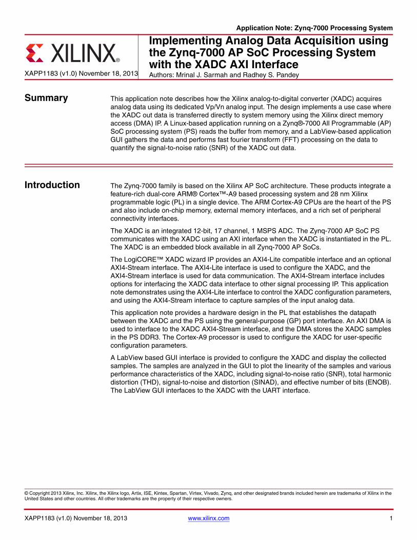
Software Architecture
The software application used in this application note is based on the Linux DMA framework driver and generic driver implementation. The application note driver invokes services exported by the Xilinx ADC DMA driver using the DMA engine API.
The software components in this application note are:
• Xilinx AXI DMA engine driver
• XADC DMA driver
• User application
• LabView GUI
Figure 2 shows the software block diagram.
Xilinx AXI DMA Engine Driver
The AXI DMA engine driver configures the Xilinx AXI DMA IP for DMA transactions. It is part of the standard Xilinx git tree.
Path: $linux-xlnx/drivers/dma/xilinx/xilinx_axidma.c
XADC DMA Driver
This driver configures AXI XADC and DMA IP. It provides a character driver interface to the user application for reading ADC samples. The driver source code is provided with this application note. The XADC DMA driver performs these steps:
1. Parses the device tree for platform specific parameters and initializes device driver structures.
2. Registers the character driver interface to the user application and provides an interface to open, read, ioctl, and close calls.
3. Allocates the DMA coherent memory for the channel (8 KB).
4. Sets up the DMA configuration (updates DMA configuration registers).
5. Initializes the event queue and configuration for each channel.
6. Configures the XADC parameters.
7. Configures the adapter block for the number of ADC samples.
X-Ref Target - Figure 2
Figure 2: Software Block Diagram

Software Architecture
XAPP1183 (v1.0) November 18, 2013 www.xilinx.com 5
AXI DMA Slave Driver
The AXI DMA slave driver communicates to the Xilinx AXI DMA driver using a Linux DMA Engine API framework. The steps for configuring a slave DMA are listed here and described in detail in this section.
1. Allocate a DMA slave channel.
2. Set slave and controller specific parameters.
3. Get a descriptor for the transaction.
4. Submit the transaction.
5. Issue pending requests and wait for callback notification.
Allocate a DMA Slave Channel
Channel allocation is slightly different in the slave DMA context. Client drivers typically need a channel from a particular DMA controller only, and in some cases even a specific channel is preferable.
To request a channel, use the dma_request_channel() API:
/* request DMA channel */
axi_xadc_dev->rx_chan = dma_request_channel(mask, axi_xadc_filter, &match);
A channel allocated via this interface is exclusive to the caller, until dma_release_channel () is called.
Set Slave and Controller Specific Parameters
The next step is passing specific information to the DMA driver. Most of the generic information that a slave DMA can use is in struct dma_slave_config. This allows the clients to specify DMA direction, DMA addresses, bus widths, DMA burst lengths, and so on for the peripheral.
To set the slave and controller specific parameters:
/* configures DMA controller parameters*/
rx_dev->device_control(axi_xadc_dev->rx_chan, DMA_SLAVE_CONFIG, (unsigned long)&config);
Get a Descriptor for Transaction
For slave usage, the various modes of slave transfers supported by the DMA engine are:
slave_sg - Fetch a list of scatter gather buffers from or to a peripheral
To get a descriptor for the transaction:
/* get handle for transaction */
rxd = rx_dev->device_prep_slave_sg(axi_xadc_dev->rx_chan, axi_xadc_dev->rx_sg, AXI_XADC_BD_COUNT, DMA_DEV_TO_MEM, axi_xadc_dev->flags, NULL);
Submit the Transaction
Once the descriptor has been prepared and the callback information added, it must be placed on the DMA engine driver pending queue.
To submit the transaction:
/* submit transaction */
axi_xadc_dev->rx_cookie = rxd->tx_submit(rxd);

Software Architecture
XAPP1183 (v1.0) November 18, 2013 www.xilinx.com 6
Issue Pending DMA Requests and Wait for Callback Notification
The transactions in the pending queue can be activated by calling the issue_pending API. If the channel is idle, then the first transaction in the queue is started and subsequent ones are queued up. On completion of each DMA operation, the next item in the queue is started and a tasklet is triggered. The tasklet calls the client driver completion callback routine for notification, if set.
To flush the pending transactions:
/*flush pending transactions */
dma_async_issue_pending(axi_xadc_dev->rx_chan);
AXI XADC Configuration
The configuration steps are:
1. Program the sequencer mode in the XADC configuration register 1.
2. Enable the Vp/Vn channel in the ADC channel selection sequencer register.
3. Write the divisor value to ADC configuration register 2.
AXI XADC DMA IOCTL Implementation
The implementation steps are:
1. AXI_XADC_DMA_CONFIG
Maps the DMA buffer for a DMA transaction:
• Initializes scatterlist array
• Configures DMA engine
• Registers DMA callback
• Submits the DMA transaction
Note: AXI_XADC_DMA_CONFIG does not start the DMA operation, but adds it to the pending queue.
2. AXI_XADC_DMA_START
Initiates the DMA transaction.
3. AXI_XADC_DMA_STOP
Terminates the DMA transaction.
Software Architecture
XAPP1183 (v1.0) November 18, 2013 www.xilinx.com 7
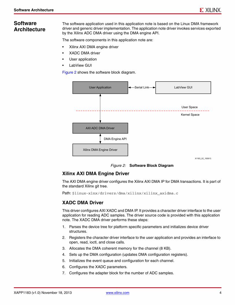
AXI XADC DMA Read Implementation
AXI XADC DMA provides an interface to copy ADC samples to the user space buffer. The driver blocks the calling user-application on the event queue after submitting and starting the DMA transaction. On the timeout of the event queue, it checks for successful completion of the DMA transaction. Then, the collected ADC samples are put into the user space buffer.
Figure 3 shows the application flow diagram.
X-Ref Target - Figure 3
Figure 3: Application Flow Diagram

Software Architecture
XAPP1183 (v1.0) November 18, 2013 www.xilinx.com 8
User Application
The user application provides an interface between the AXI XADC DMA driver and the AMS101 evaluator GUI. This application note reuses the existing AMS101 evaluator GUI, which can be downloaded from the AMS 101 Evaluation Card website. The GUI contains data acquisition and command processing modules. The GUI uses built-in LabView functions to calculate the FFT and plots the spectrum. For more details on the AMS101 evaluator GUI, see the 7 Series FPGA AMS Targeted Reference Design User Guide (UG960) [Ref 1].
Note: For information on installing the AMS101 evaluator GUI, see Chapter 2 in the AMS101 Evaluation Card User Guide (UG886) [Ref 2].
Figure 4 shows the Time Domain tab of the LabView GUI.
Note: The unipolar mode of operation of the XADC must be selected because the unipolar mode is the only mode that has been implemented in this application note. The selected sampling frequency is 961.54 KS/S. An external sinusoidal source must be connected as an analog input source.
X-Ref Target - Figure 4
Figure 4: LabView GUI Time Domain

Hardware Requirements
XAPP1183 (v1.0) November 18, 2013 www.xilinx.com 9
Figure 5 shows the Frequency Domain tab of the LabView GUI.
The data acquisition module opens the channel device node (/dev/channel01), configures and starts the DMA transaction, and puts it into a circular buffer. The command processing module configures a serial port for communication. It receives commands over a serial port from the LabView GUI in a predefined format and sends the collected samples to it for display. The user application source code is provided with this application note.
Hardware Requirements
The design can be tested using the ZC702 evaluation kit. To collect the external data using the AMS101 evaluator card, follow the instructions in the AMS101 Evaluation Card User Guide (UG886) [Ref 2] to connect the AMS101 card to the ZC702 evaluation board. An external signal can be applied to the dedicated Vp/Vn channel of the XADC embedded block, and collected samples can be read back using the LabView GUI.
X-Ref Target - Figure 5
Figure 5: LabView GUI Frequency Domain Tab

Experimental Results
XAPP1183 (v1.0) November 18, 2013 www.xilinx.com 10
Experimental Results
The XADC has been configured for a sampling frequency of 961.54 kSPS, which means the maximum signal bandwidth that can be acquired is 480 kHz. In the experimental setup, multiple frequency tones have been generated using an external sinusoid generator and the resultant signal quality metric has been calculated. In the absence of a low-pass filter in the signal generator output, the average value of SNR is close to 58 dB for a 0-1V swing.
Figure 3 summarizes the signal-to-noise ratio (SNR), total harmonic distortion (THD), and effective number of bits (ENOB) values for different input tones.
Conclusion This design provides the platform for using the AXI4-Stream interface of the XADC Wizard IP for analog data acquisition applications. The design demonstrates how to use AXI DMA to transfer the XADC samples into processor memory without processor intervention.
The design quantitatively analyzes the XADC performance metric for different frequency tones. The XADC quality metric has been measured with a non-ideal external source that generates non-coherent samples.
Reference Design
The reference design files can be downloaded from:
https://secure.xilinx.com/webreg/clickthrough.do?cid=351581
Follow the instructions provided in the readme file for building hardware and software code. Table 4 shows the reference design matrix.
See the Wiki page for rebuilding the design:
Analog Data Acquisition AXI XADC Wiki
Table 3: SNR, THD and ENOB Values
Frequency (kHz) SNR THD ENOB
1 59.17 60.15 9.44
2 59.25 59.04 9.50
5 59.24 57.64 8.54
10 59.55 57.20 8.51
Table 4: Reference Design Matrix
Parameter Description
General
Developer name Xilinx
Target devices Zynq-7000 AP SoC
Source code provided Yes
Source code format C
Design uses code and IP from existing Xilinxapplication note and reference designs,CORE Generator™ tool, or third-party
Yes
Simulation
Functional simulation performed No
Timing simulation performed No
Test bench used for functional and timing No
Simulations No

Appendix I: Device Tree
XAPP1183 (v1.0) November 18, 2013 www.xilinx.com 11
Appendix I: Device Tree
This appendix includes a portion of the DMA XADC entry in the Xilinx Linux device tree:
axi_dma_0: axidma@0x40400000 {#address-cells = <1>;#size-cells = <1>;compatible = "xlnx,axi-dma";ranges = <0x40400000 0x40400000 0x10000>;reg = <0x40400000 0x10000>;xlnx,sg-include-stscntrl-strm=<0x0>;
dma-channel@0x40400000 {compatible = "xlnx,axi-dma-s2mm-channel";interrupt-parent = <&gic>;interrupts = <0 59 4>;xlnx,datawidth = <0x08>;xlnx,genlock-mode = <0x1>;xlnx,include-dre = <0x1>;xlnx,device-id = <0x0>;
};};axi_xadc_dma: axi_xadc@0x43c00000 {#address-cells = <1>;#size-cells = <1>;compatible = "xlnx,axi-xadc-dma";reg = <0x43c00000 0x10000 0x43c10000 0x10000 >;
};
Test bench format N/A
Simulator software/version used N/A
SPICE/IBIS simulations N/A
Implementation
Synthesis software tools/version Vivado Design Suite 2013.2
Implementation software tools/versions Vivado Design Suite 2013.2
Static timing analysis performed Vivado Design Suite 2013.2
Hardware Verification
Hardware verified? Yes
Hardware platform used for verification ZC702
Table 4: Reference Design Matrix (Cont’d)
Parameter Description

Appendix II: LabView Serial Interface.
XAPP1183 (v1.0) November 18, 2013 www.xilinx.com 12
Appendix II: LabView Serial Interface.
Table 5 defines the register map for various GUI actions. The transmission over UART is the address followed by a data byte. The address limit is 16 bits and the data value is 16 bits. For Writes (16 bits of address, 16 bits of write data), 'OK' acknowledgement is provided. For Reads, R AAAA is followed by read data.
References This document uses the following references:
1. 7 Series FPGA AMS Targeted Reference Design User Guide (UG960)
2. AMS101 Evaluation Card User Guide (UG886)
3. Zynq-7000 All Programmable SoC Technical Reference Manual (UG585)
4. 7 Series FPGAs and Zynq-7000 All Programmable SoC XADC Dual 12-Bit 1 MSPS Analog-to-Digital Converter User Guide (UG480)
5. DMA Engine API Guide (Documentation/dmaengine.txt)
6. AMS 101 Evaluation Card website
7. Analog Data Acquisition AXI XADC Wiki
Table 5: Register Map for GUI Actions
GUI Commands/Clicks UART Transmission UART Reception
Address Data
Connection establishment: Design version register (read-only)
0x0000 Read-only design version register. Returns 16-bits of data. Design version (D11-8).(D7-0)
D15-12 indicates the device family (because the same GUI can be used for designs in different families)
0001 - Artix®-7
0010 - Kintex®-7
0011 - Virtex®-7
For KC705 designs, it returns 0x2100.
UART command: R 0000
Time domain/frequency Domain tab:collect data (read-only)
0x0001 FPGA sends back 4096 samples (8K bytes) of raw data for further processing by LV-GUI
For simultaneous sampling mode, need dual display and FFT returns 8192 samples with even samples corresponding to VAUX[0] channel and odd samples corresponding to VAUX[8] channel
UART Command: R 0001

Revision History
XAPP1183 (v1.0) November 18, 2013 www.xilinx.com 13
Revision History
The following table shows the revision history for this document.
Notice of Disclaimer
The information disclosed to you hereunder (the “Materials”) is provided solely for the selection and use ofXilinx products. To the maximum extent permitted by applicable law: (1) Materials are made available "ASIS" and with all faults, Xilinx hereby DISCLAIMS ALL WARRANTIES AND CONDITIONS, EXPRESS,IMPLIED, OR STATUTORY, INCLUDING BUT NOT LIMITED TO WARRANTIES OFMERCHANTABILITY, NON-INFRINGEMENT, OR FITNESS FOR ANY PARTICULAR PURPOSE; and (2)Xilinx shall not be liable (whether in contract or tort, including negligence, or under any other theory ofliability) for any loss or damage of any kind or nature related to, arising under, or in connection with, theMaterials (including your use of the Materials), including for any direct, indirect, special, incidental, orconsequential loss or damage (including loss of data, profits, goodwill, or any type of loss or damagesuffered as a result of any action brought by a third party) even if such damage or loss was reasonablyforeseeable or Xilinx had been advised of the possibility of the same. Xilinx assumes no obligation tocorrect any errors contained in the Materials or to notify you of updates to the Materials or to productspecifications. You may not reproduce, modify, distribute, or publicly display the Materials without priorwritten consent. Certain products are subject to the terms and conditions of the Limited Warranties whichcan be viewed at http://www.xilinx.com/warranty.htm; IP cores may be subject to warranty and supportterms contained in a license issued to you by Xilinx. Xilinx products are not designed or intended to befail-safe or for use in any application requiring fail-safe performance; you assume sole risk and liability foruse of Xilinx products in Critical Applications: http://www.xilinx.com/warranty.htm#critapps.
Date Version Description of Revisions
11/18/2013 1.0 Initial Xilinx release.
Related Documents