STPC ATLAS X86 PC Compatible Information Appliance System-on-Chip PRODUCT PREVIEW 1/82 12/4/01 Issue 1.0 This is preliminary information on a new product now in development or undergoing evaluation. Details are subject to change without notice. Figure 0-1. Logic Diagram ■ POWERFUL x86 PROCESSOR ■ 64-BIT SDRAM UMA CONTROLLER ■ GRAPHICS CONTROLLER - VGA & SVGA CRT CONTROLLER - 135MHz RAMDAC - ENHANCED 2D GRAPHICS ENGINE ■ VIDEO INPUT PORT ■ VIDEO PIPELINE - UP-SCALER - VIDEO COLOUR SPACE CONVERTER - CHROMA & COLOUR KEY SUPPORT ■ TFT DISPLAY CONTROLLER ■ PCI 2.1 COMPLIANT MASTER / SLAVE/ ARBITER ■ ISA MASTER / SLAVE CONTROLLER ■ 16-BIT LOCAL BUS INTERFACE ■ PCMCIA INTERFACE CONTROLLER ■ Ultra DMA-33 IDE CONTROLLER ■ 2 USB HOST HUB INTERFACES ■ I/O FEATURES - PC/AT+ KEYBOARD CONTROLLER - PS/2 MOUSE CONTROLLER - 2 SERIAL PORTS - 1 PARALLEL PORT - 16 GENERAL PURPOSE I/Os - I C INTERFACE ■ INTEGRATED PERIPHERAL CONTROLLER - DMA CONTROLLER - INTERRUPT CONTROLLER - TIMER / COUNTERS ■ POWER MANAGEMENT UNIT ■ WATCHDOG ■ JTAG IEEE1149.1 PBGA516 S TP C A t l as x86 Host SDRAM SVGA GE I/F VIP PCI m/s LB PCI Bus ISA IPC PCI ISA Bus CRTC Cursor Moni tor IDE PMU Video C Key K Key Local Bus PCMCIA I/Os USB TFT TFT I/F Video In

Welcome message from author
This document is posted to help you gain knowledge. Please leave a comment to let me know what you think about it! Share it to your friends and learn new things together.
Transcript

STPC ATLAS
X86 PC Compatible Information Appliance System-on-ChipPRODUCT PREVIEW
1/8212/4/01Issue 1.0
This is preliminary information on a new product now in development or undergoing evaluation. Details are subject to change without notice.
Figure 0-1. Logic Diagram
POWERFUL x86 PROCESSOR
64-BIT SDRAM UMA CONTROLLER
GRAPHICS CONTROLLER- VGA & SVGA CRT CONTROLLER- 135MHz RAMDAC- ENHANCED 2D GRAPHICS ENGINE
VIDEO INPUT PORT
VIDEO PIPELINE- UP-SCALER- VIDEO COLOUR SPACE CONVERTER- CHROMA & COLOUR KEY SUPPORT
TFT DISPLAY CONTROLLER
PCI 2.1 COMPLIANT MASTER / SLAVE/ARBITER
ISA MASTER / SLAVE CONTROLLER
16-BIT LOCAL BUS INTERFACE
PCMCIA INTERFACE CONTROLLER
Ultra DMA-33 IDE CONTROLLER
2 USB HOST HUB INTERFACES
I/O FEATURES- PC/AT+ KEYBOARD CONTROLLER- PS/2 MOUSE CONTROLLER- 2 SERIAL PORTS- 1 PARALLEL PORT- 16 GENERAL PURPOSE I/Os- I C INTERFACE
INTEGRATED PERIPHERAL CONTROLLER- DMA CONTROLLER- INTERRUPT CONTROLLER- TIMER / COUNTERS
POWER MANAGEMENT UNIT
WATCHDOG
JTAG IEEE1149.1
PBGA516
STPCAtlas
x86Host
SDRAM
SVGA
GE I/F
VIP
PCIm/s
LB
PCI Bus
ISAIPC PCI
ISA Bus
CRTCCursor
Monitor
IDE
PMU
VideoC Key
K Key
Local Bus
PCMCIA
I/Os
USB
TFTTFT I/F
Video In

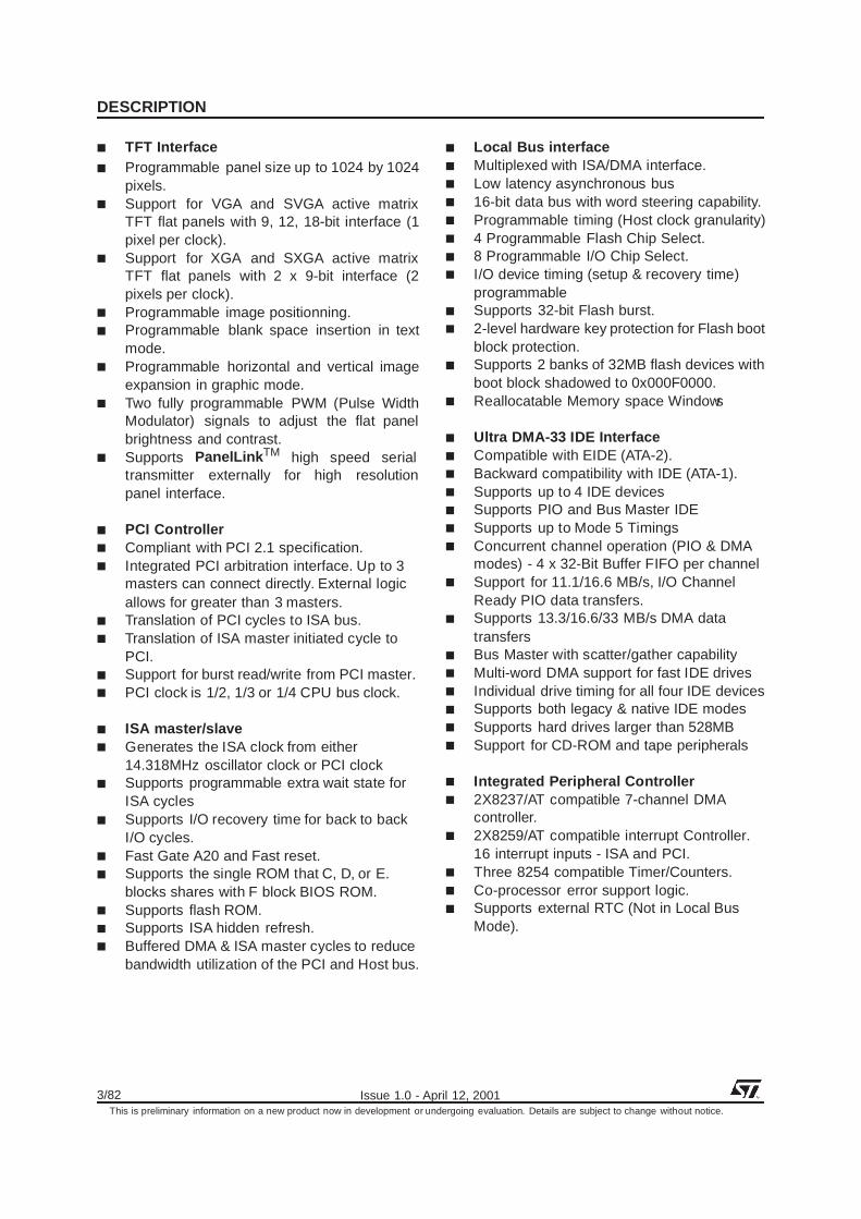
DESCRIPTION
Issue 1.0 - April 12, 2001 2/82This is preliminary information on a new product now in development or undergoing evaluation. Details are subject to change without notice.
DESCRIPTIONThe STPC Atlas integrates a standard 5th genera-tion x86 core along with a powerful UMA graphics/video chipset, support logic including PCI, ISA,Local Bus, USB, UIDE controllers and combinesthem with standard I/O interfaces to provide a sin-gle PC compatible subsystem on a single device,suitable for all kinds of terminal and industrial ap-pliances.
X86 Processor core Fully static 32-bit 5-stage pipeline, x86
processor fully PC compatible. Can access up to 4GB of external memory. 8Kbyte unified instruction and data cache
with write back and write through capability. Parallel processing integral floating point unit,
with automatic power down. Runs up to 100MHz (X1) or 133 MHz (X2). Fully static design for dynamic clock control. Low power and system management modes. Optimized design for 2.5V operation.
SDRAM Controller 64-bit data bus. Up to 100MHz SDRAM clock speed. Integrated system memory, graphic frame
memory and video frame memory. Supports 8MB up to 128 MB system memory. Supports 16-Mbit, 64-Mbit and 128-Mbit
SDRAMs. Supports 8, 16, 32, 64, and 128 MB DIMMs. Supports buffered, non buffered, and
registered DIMMs 4-line write buffers for CPU to DRAM and PCI
to DRAM cycles. 4-line read prefetch buffers for PCI masters. Programmable latency Programmable timing for SDRAM
parameters. Supports -8, -10, -12, -13, -15 memory parts Supports memory hole between 1MB and
8MB for PCI/ISA busses. 32-bit access, Autoprecharge & Power-down
are not supported.
Enhanced 2D Graphics Controller Supports pixel depths of 8, 16, 24 and 32 bit. Full BitBLT implementation for all 256 raster
operations defined for Windows. Supports 4 transparent BLT modes - Bitmap
Transparency, Pattern Transparency, SourceTransparency and Destination Transparency.
Hardware clipping Fast line draw engine with anti-aliasing. Fast triangle fill engine. Supports 4-bit alpha blended font for anti-
aliased text display. Complete double buffered registers for
pipelined operation. 64-bit wide pipelined architecture running at
100 MHz. Hardware clipping
CRT Controller Integrated 135MHz triple RAMDAC allowing
for 1280 x 1024 x 75Hz display. 8-, 16-, 24-bit pixels. Interlaced or non-interlaced output.
Video Input port Accepts video inputs in CCIR 601/656 mode. Optional 2:1 decimator Stores captured video in off setting area of
the onboard frame buffer. HSYNC and B/T generation or lock onto
external video timing source.
Video Pipeline Two-tap interpolative horizontal filter. Two-tap interpolative vertical filter. Color space conversion (RGB to YUV and
YUV to RGB). Programmable window size. Chroma and color keying for integrated video
overlay.
DESCRIPTION
3/82 Issue 1.0 - April 12, 2001This is preliminary information on a new product now in development or undergoing evaluation. Details are subject to change without notice.
TFT Interface Programmable panel size up to 1024 by 1024
pixels. Support for VGA and SVGA active matrix
TFT flat panels with 9, 12, 18-bit interface (1pixel per clock).
Support for XGA and SXGA active matrixTFT flat panels with 2 x 9-bit interface (2pixels per clock).
Programmable image positionning. Programmable blank space insertion in text
mode. Programmable horizontal and vertical image
expansion in graphic mode. Two fully programmable PWM (Pulse Width
Modulator) signals to adjust the flat panelbrightness and contrast.
Supports PanelLink TM high speed serialtransmitter externally for high resolutionpanel interface.
PCI Controller Compliant with PCI 2.1 specification. Integrated PCI arbitration interface. Up to 3
masters can connect directly. External logicallows for greater than 3 masters.
Translation of PCI cycles to ISA bus. Translation of ISA master initiated cycle to
PCI. Support for burst read/write from PCI master. PCI clock is 1/2, 1/3 or 1/4 CPU bus clock.
ISA master/slave Generates the ISA clock from either
14.318MHz oscillator clock or PCI clock Supports programmable extra wait state for
ISA cycles Supports I/O recovery time for back to back
I/O cycles. Fast Gate A20 and Fast reset. Supports the single ROM that C, D, or E.
blocks shares with F block BIOS ROM. Supports flash ROM. Supports ISA hidden refresh. Buffered DMA & ISA master cycles to reduce
bandwidth utilization of the PCI and Host bus.
Local Bus interface Multiplexed with ISA/DMA interface. Low latency asynchronous bus 16-bit data bus with word steering capability. Programmable timing (Host clock granularity) 4 Programmable Flash Chip Select. 8 Programmable I/O Chip Select. I/O device timing (setup & recovery time)
programmable Supports 32-bit Flash burst. 2-level hardware key protection for Flash boot
block protection. Supports 2 banks of 32MB flash devices with
boot block shadowed to 0x000F0000. Reallocatable Memory space Windows
Ultra DMA-33 IDE Interface Compatible with EIDE (ATA-2). Backward compatibility with IDE (ATA-1). Supports up to 4 IDE devices Supports PIO and Bus Master IDE Supports up to Mode 5 Timings Concurrent channel operation (PIO & DMA
modes) - 4 x 32-Bit Buffer FIFO per channel Support for 11.1/16.6 MB/s, I/O Channel
Ready PIO data transfers. Supports 13.3/16.6/33 MB/s DMA data
transfers Bus Master with scatter/gather capability Multi-word DMA support for fast IDE drives Individual drive timing for all four IDE devices Supports both legacy & native IDE modes Supports hard drives larger than 528MB Support for CD-ROM and tape peripherals
Integrated Peripheral Controller 2X8237/AT compatible 7-channel DMA
controller. 2X8259/AT compatible interrupt Controller.
16 interrupt inputs - ISA and PCI. Three 8254 compatible Timer/Counters. Co-processor error support logic. Supports external RTC (Not in Local Bus
Mode).

DESCRIPTION
Issue 1.0 - April 12, 2001 4/82This is preliminary information on a new product now in development or undergoing evaluation. Details are subject to change without notice.
PCMCIA interface Support one PCMCIA 2.0 / JEIDA 4.1 68-pin
standard PC Card Socket. Power Management support. Support PCMCIA/ATA specifications. Support I/O PC Card with pulse-mode
interrupts. Provides an ExCATM implementation to
PCMCIA 2.0 / JEIDA 4.1 standards.
USB Interface USB 1.1 compatible. Open HCI 1.0 compliant. User configurable RootHub. Support for both LowSpeed and HighSpeed
USB devices. No bi-directionnal or Tri-state busses. No level sensitive latches. System Management Interrupt pin support Hooks for legacy device support.
Keyboard interface Fully PC/AT+ compatible
Mouse interface Fully PS/2 compatible
Serial interface 15540 compatible Programmable word length, stop bits, parity. 16-bit programmable baud rate generator. Interrupt generator. Loop-back mode. 8-bit scratch register. Two 16-bit FIFOs. Two DMA handshake lines.
Parallel port All IEEE Standard 1284 protocols supported:
Compatibility, Nibble, Byte, EPP, and ECPmodes.
16 bytes FIFO for ECP.
Power Management Four power saving modes: On, Doze,
Standby, Suspend. Programmable system activity detector Supports Intel & Cyrix SMM and APM. Supports STOPCLK. Supports IO trap & restart. Independent peripheral time-out timer to
monitor hard disk, serial & parallel port. 128K SM_RAM address space from
0xA0000 to 0xB0000
JTAG Boundary Scan compatible IEEE1149.1. Scan Chain control. Bypass register compatible IEEE1149.1. ID register compatible IEEE1149.1. RAM BIST control.
.
ExCA is a trademark of PCMCIA / JEIDA.
PanelLink is a trademark of SiliconImage, Inc

DESCRIPTION
5/82 Issue 1.0 - April 12, 2001This is preliminary information on a new product now in development or undergoing evaluation. Details are subject to change without notice.

GENERAL DESCRIPTION
Issue 1.0 - April 12, 2001 6/82This is preliminary information on a new product now in development or undergoing evaluation. Details are subject to change without notice.
1 GENERAL DESCRIPTION
At the heart of the STPC Atlas is an advancedprocessor block that includes a powerful x86 proc-essor core along with a 64-bit SDRAM controller,advanced 64-bit accelerated graphics and videocontroller, a high speed PCI local-bus controllerand Industry standard PC chip set functions (Inter-rupt controller, UltraDMA IDE Controller, Intervaltimer and ISA bus).
The STPC Atlas has in addition, a TFT output, aVideo Input, a Local Bus interface, PCMCIA andsuper I/O features including USB host hub.
The STPC Atlas makes use of a tightly coupledUnified Memory Architecture (UMA), where thesame memory array is used for CPU main memo-ry and graphics frame-buffer. This means a reduc-tion in total system memory for system perform-ances that are equal to that of a comparable framebuffer and system memory based system, andgenerally much better, due to the higher memorybandwidth allowed by attaching the graphics en-gine directly to the 64-bit processor host interfacerunning at the speed of the processor bus ratherthan the traditional PCI bus.
The 64-bit wide memory array provides the sys-tem with an 800MB/s peak bandwidth. This allowsfor higher resolution screens and greater colordepth. The processor bus runs at 133 MHz, furtherincreasing “standard” bandwidth by at least a fac-tor of two.
The ‘standard’ PC chipset functions (DMA, inter-rupt controller, timers, power management logic)are integrated together with the x86 processorcore; additional low bandwidth functions such ascommunication ports are accessed by the STPCAtlas via an internal ISA bus.
The PCI bus is the main data communication linkto the STPC Atlas chip. The STPC Atlas translatesappropriate host bus I/O and Memory cycles ontothe PCI bus. It also supports the generation ofConfiguration cycles on the PCI bus. The STPCAtlas, as a PCI bus agent (host bridge class), fullycomplies with PCI specification 2.1. The chip-setalso implements the PCI mandatory header regis-ters in Type 0 PCI configuration space for easyporting of PCI aware system BIOS. The devicecontains a PCI arbitration function for three exter-nal PCI devices.
Graphics functions are controlled through the on-chip SVGA controller and the monitor display isproduced through the 2D graphics display engine.
This Graphics Engine is tuned to work with thehost CPU to provide a balanced graphics systemwith a low silicon area cost. It performs limitedgraphics drawing operations which include hard-ware acceleration of text, bitblts, transparent bltsand fills. The results of these operations changethe contents of the on-screen or off-screen framebuffer areas of SDRAM memory. The frame buffercan occupy a space up to 4 Mbytes anywhere inthe physical main memory.
The maximum graphics resolution supported is1280 x 1024 in 16 Million colours at 75 Hz refreshrate and is VGA and SVGA compatible. Horizontaltiming fields are VGA compatible while the verticalfields are extended by one bit to accommodateabove display resolution.
To generate the TFT output, the STPC Atlas ex-tracts the digital video stream before the RAM-DAC and reformats it to the TFT format. Theheight and width of the flat panel are programma-ble through configuration registers up to a size of1024 by 1024.
By default, lower resolution images cover only apart of the larger TFT panel. The STPC Atlas al-lows the user to expand the image vertically andhorizontally in text mode by inserting programma-ble blank pixels. It allows expansion of the imagevertically and horizontally in graphics mode byreplicating pixels. The replication of J times everyK pixel is independently programmable in the ver-tical and horizontal directions.
PanelLink TM is a proprietary interconnect protocoldefined by Silicon Image, Inc. It consists of atransmitter that takes parallel video/graphics datafrom the host LCD graphics controller and trans-mits it serially at high speed to the receiver whichcontrols the TFT panel. The TFT interface is de-signed to support the connection of this controlsignal to the PanelLink TM transmitter.
The STPC Atlas PCMCIA controller has been spe-cifically designed to provide the interface with PC-Cards which contain additional memory or I/O andprovides an ExCATM implementation to PCMCIA2.0 / JEIDA 4.1 standards.
The power management control facilities includesocket power control, insertion/removal capability,power saving with Windows inactivity, NCS con-

GENERAL DESCRIPTION
7/82 Issue 1.0 - April 12, 2001This is preliminary information on a new product now in development or undergoing evaluation. Details are subject to change without notice.
trolled Chip Power Down, together with furthercontrols for 3.3V suspend with Modem RingResume Detection.
The need for system configuration jumpers iseliminated by providing address mapping supportfor PCMCIA 2.0 / JEIDA 4.1 PC-Card memory to-gether with address windowing support for I/Ospace.
The STPC Atlas implements a multi-function par-allel port. The standard PC/AT compatible logicaladdress assignments for LPT1, LPT2 and LPT3are supported.
The parallel port can be configured for any of thefollowing three modes and supports the IEEEStandard 1284 parallel interface protocol stand-ards, as follows:
- Compatibility Mode (Forward channel, standard)
- Nibble Mode (Reverse channel, PC compatible)
- Byte Mode (Reverse channel, PS/2 compatible)
The STPC Atlas BGA package has 516 balls. Thishowever is not sufficient for all of the integratedfunctions available; some features therefore sharethe same balls and cannot thus be used at thesame time. The STPC Atlas configuration is doneby ‘strap options’. This is a set of pull-up or pull-down resistors on the memory data bus, checkedon reset, which auto-configure the STPC Atlas.
There are three distinguishable independentlyconfigurable main blocks: The ISA block, the Lo-cal Bus block and the PCI/PC Card block.
From the first two blocks, either the ISA bus andsome IPC additional features can be activated, oralternatively, the Local bus, the parallel port andthe second serial interface.
From the third block, either the PCI bus can be ac-tivated, or the PC Card interface (PCMCIA).
The STPC Atlas core is compliant with the Ad-vanced Power Management (APM) specificationto provide a standard method by which the BIOScan control the power used by personal comput-ers. The Power Management Unit (PMU) modulecontrols the power consumption, providing a com-prehensive set of features that controls the powerusage and supports compliance with the UnitedStates Environmental Protection Agency’s EnergyStar Computer Program. The PMU provides thefollowing hardware structures to assist the soft-ware in managing the system power consumption:
- System Activity Detection.
- Three power-down timers detecting system inac-tivity:
- Doze timer (short durations).
- Stand-by timer (medium durations).
- Suspend timer (long durations).
- House-keeping activity detection.
- House-keeping timer to cope with short bursts ofhouse-keeping activity while dozing or in stand-bystate.
- Peripheral activity detection.
- Peripheral timer detecting peripheral inactivity
- SUSP# modulation to adjust the system perform-ance in various power down states of the systemincluding full power-on state.
- Power control outputs to disable power from dif-ferent planes of the board.
Lack of system activity for progressively longerperiods of time is detected by the three powerdown timers. These timers can generate SMI in-terrupts to CPU so that the SMM software can putthe system in decreasing states of power con-sumption. Alternatively, system activity in a powerdown state can generate an SMI interrupt to allowthe software to bring the system back up to fullpower-on state. The chip-set supports up to threepower down states described above; these corre-spond to decreasing levels of power savings.
Power down puts the STPC Atlas into suspendmode. The processor completes execution of thecurrent instruction, any pending decoded instruc-tions and associated bus cycles. During the sus-pend mode, internal clocks are stopped. Remov-ing power-down, the processor resumes instruc-tion fetching and begins execution in the instruc-tion stream at the point it had stopped. Because ofthe static nature of the core, no internal data islost.
An industry standard EIDE (ATA 2) controller isbuilt in to the STPC Atlas and connected internallyvia the PCI bus.
The STPC Atlas has three additional features;USB, GPIO and JTAG. These are described brief-ly below.
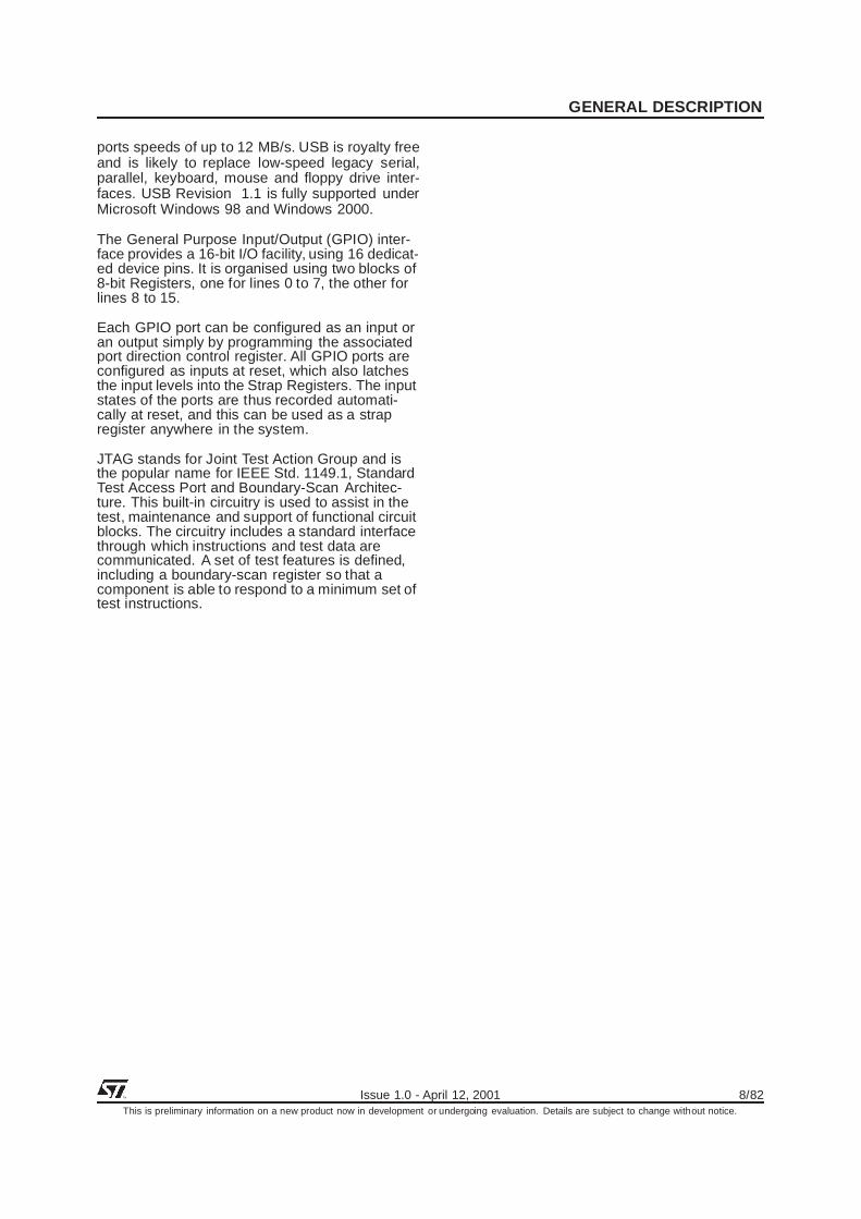
Universal Serial Bus (USB) is a general purposecommunications interface for connecting peripher-als to a PC. The USB Open Host Controller Inter-face (Open HCI) Specification, revision 1.1, sup-
GENERAL DESCRIPTION
Issue 1.0 - April 12, 2001 8/82This is preliminary information on a new product now in development or undergoing evaluation. Details are subject to change without notice.
ports speeds of up to 12 MB/s. USB is royalty freeand is likely to replace low-speed legacy serial,parallel, keyboard, mouse and floppy drive inter-faces. USB Revision 1.1 is fully supported underMicrosoft Windows 98 and Windows 2000.
The General Purpose Input/Output (GPIO) inter-face provides a 16-bit I/O facility, using 16 dedicat-ed device pins. It is organised using two blocks of8-bit Registers, one for lines 0 to 7, the other forlines 8 to 15.
Each GPIO port can be configured as an input oran output simply by programming the associatedport direction control register. All GPIO ports areconfigured as inputs at reset, which also latchesthe input levels into the Strap Registers. The inputstates of the ports are thus recorded automati-cally at reset, and this can be used as a strapregister anywhere in the system.
JTAG stands for Joint Test Action Group and isthe popular name for IEEE Std. 1149.1, StandardTest Access Port and Boundary-Scan Architec-ture. This built-in circuitry is used to assist in thetest, maintenance and support of functional circuitblocks. The circuitry includes a standard interfacethrough which instructions and test data arecommunicated. A set of test features is defined,including a boundary-scan register so that acomponent is able to respond to a minimum set oftest instructions.

GENERAL DESCRIPTION
9/82 Issue 1.0 - April 12, 2001This is preliminary information on a new product now in development or undergoing evaluation. Details are subject to change without notice.
Figure 1-1. Functional description.
x86
Core
Host
I/F
SDRAM
CTRL
SVGA
GE I/F
VIP
PCI m/s
LB
CTRL
PCI Bus
ISA
m/s
IPCPCI
m/s
ISA Bus
CRTC
Cursor
Monitor
IDE
I/F
PMU
Video
Pipeline C Key
K Key
LUT
Local Bus
PCMCIA
I/Os
USB
TFTTFT I/F
Video In
JTAG

GENERAL DESCRIPTION
Issue 1.0 - April 12, 2001 10/82This is preliminary information on a new product now in development or undergoing evaluation. Details are subject to change without notice.
Figure 1-2. Typical PC oriented Application
ISA
PCI
SDRAMs
Flash
UIDE
Serial Ports
Parallel Port
Floppy
Monitor
TFTSVGAIRQ
DMA.REQ
DMA.ACK
STPC Atlas
Mouse
Keyboard
USB
Boot
VIP

GENERAL DESCRIPTION
11/82 Issue 1.0 - April 12, 2001This is preliminary information on a new product now in development or undergoing evaluation. Details are subject to change without notice.
Figure 1-3. Typical Embedded Application
STPC Atlas
SDRAMs
Flash
IRQ
PCMCIA
Monitor
TFT
SVGA
Mouse
Keyboard
Serial Ports
Parallel Port
STPC Local Bus
SRAM
RTC I2C
USB

STRAP OPTION
Issue 1.0 - April 12, 2001 12/82This is preliminary information on a new product now in development or undergoing evaluation. Details are subject to change without notice.
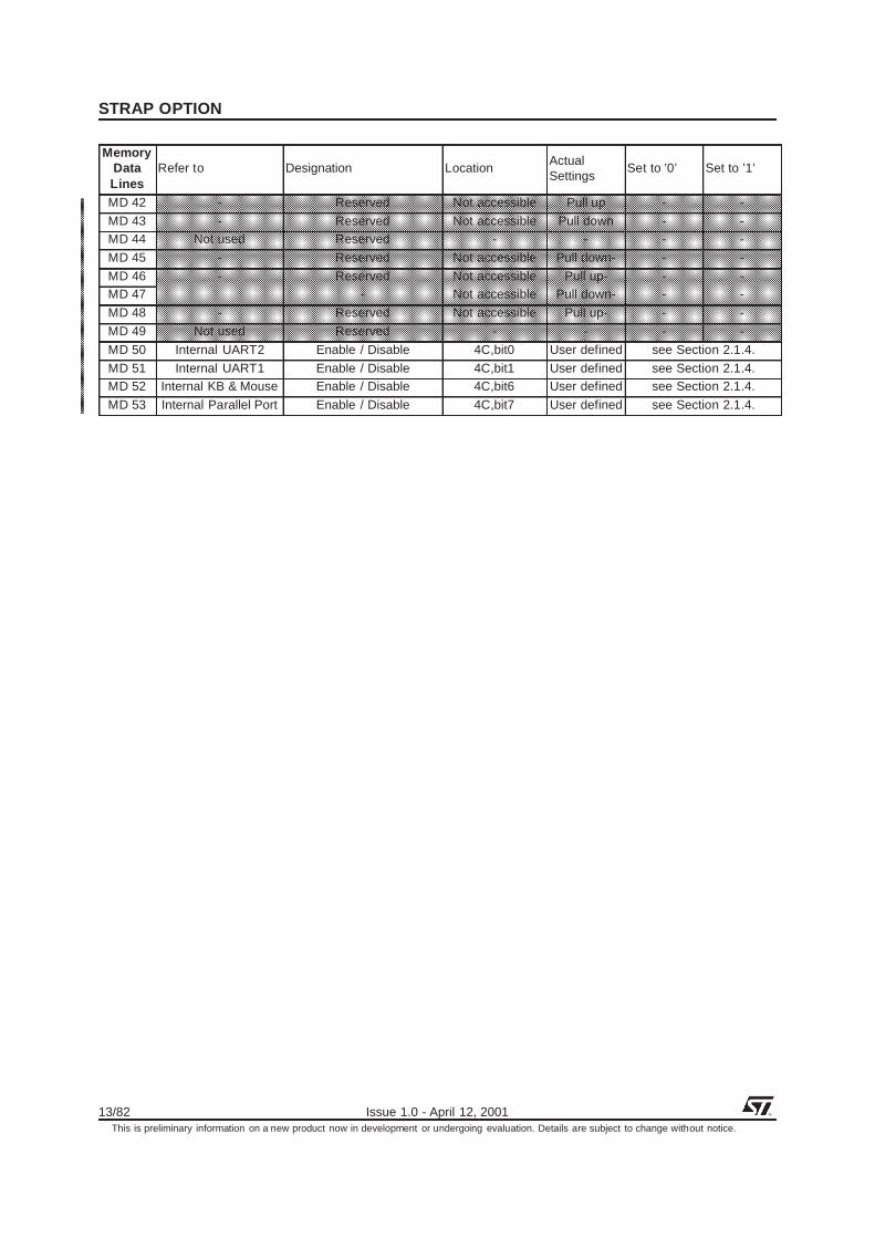
2. STRAP OPTION
This chapter defines the STPC Atlas StrapOptions and their locations. Some strap options
are left programmable for future versions ofsilicon.
MemoryDataLines
Refer to Designation LocationActualSettings
Set to ’0’ Set to ’1’
MD0 Not used Reserved - - - -
MD1 Reserved DAC Test Mode Not accessible Pull Up - -MD2
HCLK SpeedIndex 5F,bit 6 User defined
See Section 2.1.3.MD3 Index 5F,bit 7 User defined
MD4 PCI Clock PCI_CLKO Divisor Index 4A,bit 1 User defined See Section 2.1.1.MD5 Memory Clock MCLK Synch Index 4A,bit 2 User defined See Section 2.1.1.
MD6PCICLK PCICKLO Programming
Index 4A,bit 6 User definedSee Section 2.1.1.
MD7 Index 4A,bit 7 User defined
MD8Mode Select ISA/PCMCIA/Local Bus
Index 4A,bit 3 User definedSee Section 2.1.1.
MD9 Index 4A,bit 3 User definedMD10
PCICLKPCICLK Deskew
Programming
Index 4B,bit 2 User defined
See Section 2.1.2.MD11 Index 4B,bit 3 User defined
MD12 Index 4B,bit 4 User definedMD13 Index 4B,bit 5 User defined
MD14 CPU Clock CPUCLK Multiplication Index 4B,bit 6 User defined See Section 2.1.2.
MD15 - Reserved Not accessible Pull up - -MD16 - Reserved Not accessible Pull up - -
MD17 PCI Clock PCI_CLKO Divisor Index 4A,bit 0 User defined See Section 2.1.1.
MD18 Host Clock HCLK Pad Direction Index 4C,bit 2 User defined External Internal
MD19 Memory Clock MCLK Pad Direction Index 4C,bit 3 User defined External Internal
MD20 DOT Clock DCLK Pad Direction Index 4C,bit 4 User defined External InternalMD21 IPC Test Mode Reserved Index 5F,bit 0 Pull up - -
MD22 Not used Reserved - - - -
MD23 - Reserved Index 5F,bit 2 Pull up - -MD24
HCLK HCLK PLL Speed
Index 5F,bit 3 User defined
See Section 2.1.3.MD25 Index 5F,bit 4 User defined
MD26 Index 5F,bit 5 User definedMD27 - Reserved Not accessible Pull up- - -
MD28 - Reserved Not accessible Pull up- - -
MD29 - Reserved Not accessible Pull up- - -
MD30 - Reserved Not accessible Pull up- - -
MD31 - Reserved Not accessible - - -MD32 - Reserved Not accessible - - -
MD33 - Reserved Not accessible - - -
MD34 - Reserved Not accessible - - -MD35 - Reserved Not accessible - - -
MD 36 Local Bus Boot Device Selection 4B,bit 0 User defined 8 bit 16 bit
MD 37 Reserved Not accessible Pull upMD 38 Reserved Not accessible Pull up
MD 39 Reserved Not accessible Pull up
MD 40 CPU Clock CPUCLK Multiplication Index 4B,bit 7 User defined See Section 2.1.2.
MD 41 - Reserved Not accessible Pull down - -
STRAP OPTION
13/82 Issue 1.0 - April 12, 2001This is preliminary information on a new product now in development or undergoing evaluation. Details are subject to change without notice.
MD 42 - Reserved Not accessible Pull up - -
MD 43 - Reserved Not accessible Pull down - -MD 44 Not used Reserved - - - -
MD 45 - Reserved Not accessible Pull down- - -
MD 46 - Reserved Not accessible Pull up- - -MD 47 - Not accessible Pull down- - -
MD 48 - Reserved Not accessible Pull up- - -
MD 49 Not used Reserved - - - -
MD 50 Internal UART2 Enable / Disable 4C,bit0 User defined see Section 2.1.4.
MD 51 Internal UART1 Enable / Disable 4C,bit1 User defined see Section 2.1.4.MD 52 Internal KB & Mouse Enable / Disable 4C,bit6 User defined see Section 2.1.4.
MD 53 Internal Parallel Port Enable / Disable 4C,bit7 User defined see Section 2.1.4.
MemoryDataLines
Refer to Designation LocationActualSettings
Set to ’0’ Set to ’1’
STRAP OPTION
Issue 1.0 - April 12, 2001 14/82This is preliminary information on a new product now in development or undergoing evaluation. Details are subject to change without notice.
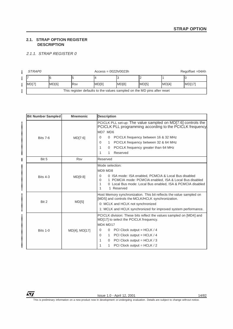
2.1. STRAP OPTION REGISTERDESCRIPTION
2.1.1. STRAP REGISTER 0
STRAP0 Access = 0022h/0023h Regoffset =04Ah
7 6 5 4 3 2 1 0
MD[7] MD[6] Rsv MD[9] MD[8] MD[5] MD[4] MD[17]
This register defaults to the values sampled on the MD pins after reset
Bit Number Sampled Mnemonic Description
Bits 7-6 MD[7:6]
PCICLK PLL set-up: The value sampled on MD[7:6] controls thePCICLK PLL programming according to the PCICLK frequency.MD7 MD6
0 0 PCICLK frequency between 16 & 32 MHz
0 1 PCICLK frequency between 32 & 64 MHz
1 0 PCICLK frequency greater than 64 MHz
1 1 Reserved
Bit 5 Rsv Reserved
Bits 4-3 MD[9:8]
Mode selection:
MD9 MD8
0 0 ISA mode: ISA enabled, PCMCIA & Local Bus disabled0 1 PCMCIA mode: PCMCIA enabled, ISA & Local Bus disabled1 0 Local Bus mode: Local Bus enabled, ISA & PCMCIA disabled1 1 Reserved
Bit 2 MD[5]
Host Memory synchronization. This bit reflects the value sampled on[MD5] and controls the MCLK/HCLK synchronization.
0: MCLK and HCLK not synchronized
1: MCLK and HCLK synchronized for improved system performance.
Bits 1-0 MD[4], MD[17]
PCICLK division: These bits reflect the values sampled on [MD4] andMD[17] to select the PCICLK frequency.
MD4 MD17
0 0 PCI Clock output = HCLK / 4
0 1 PCI Clock output = HCLK / 4
1 0 PCI Clock output = HCLK / 3
1 1 PCI Clock output = HCLK / 2

STRAP OPTION
15/82 Issue 1.0 - April 12, 2001This is preliminary information on a new product now in development or undergoing evaluation. Details are subject to change without notice.
2.1.2. STRAP REGISTER 1
STRAP1 Access = 0022h/0023h Regoffset =04Bh
7 6 5 4 3 2 1 0
MD[40] MD[14] MD[13] MD[12] MD[11] MD[10] Rsd MD[36]
This register defaults to the values sampled on the MD pins after reset
Bit Number Sampled Mnemonic Description
Bits 7-6 MD[40] & MD[14]
CPU Clock Multiplication (486 mode):
MD40 MD14
0 0 Reserved
0 1 X 1
1 0 X 3
1 1 X 2The default is pull down resistor to MD[40], pull up resistor to MD[14], toselect DX1 mode.
Bits 5-2 MD[13:10]
PCI Clock deskew programming:
MD[10]: 0: Deskew programming enabled1: Deskew programming bypassed
MD[11]: 0: Default programming start used1: User control of programming using MD[12-13] (bits 5-4)
MD[13:12]: MD[13] set to 1 to program 2 MSB deskew delay start point.
Bit 1 Rsv Reserved
Bit 0 MD[36]
These bits reflect thevalues sampled on MD[36] and deter-mines the Local Bus Boot device width:0: 8-bit Boot Device supported1: 16-bit Boot Device supported

STRAP OPTION
Issue 1.0 - April 12, 2001 16/82This is preliminary information on a new product now in development or undergoing evaluation. Details are subject to change without notice.
2.1.3. HCLK PLL STRAP REGISTER
Table 2-1. HCLK Frequency Programming
HCLK_STRAP0 Access = 0022h/0023h Regoffset =05Fh
7 6 5 4 3 2 1 0
MD[3] MD[2] MD[26] MD[25] MD[24] Rsv
This register defaults to the values sampled on the MD pins after reset
Bit Number Sampled Mnemonic Description
Bits 7-3 MD[3:2] & MD[26:24]These pins reflect the values sampled on MD[3:2] and MD[26:24] pins re-spectively and control the Host clock frequency synthesizer as shown inTable 2-2
Bits 2-0 Rsv Reserved
MD[3] MD[2] MD[26] MD[25] MD[24] HCLK Speed0 0 0 0 0 25 MHz0 0 0 0 1 50 MHz
0 0 0 1 0 60 MHz
0 0 0 1 1 66 MHz0 1 0 0 1 75 MHz
1 0 0 1 1 90 MHz
1 1 0 0 1 100 MHz1 1 1 1 1 133 MHz

STRAP OPTION
17/82 Issue 1.0 - April 12, 2001This is preliminary information on a new product now in development or undergoing evaluation. Details are subject to change without notice.
2.1.4. STRAP REGISTER 2
.
STRAP2 Access = 0022h/0023h Regoffset =04Ch
7 6 5 4 3 2 1 0
MD[53] MD[52] Rsv MD[20] MD[19] MD[18] MD[51] MD[50]
This register defaults to the values sampled on the MD pins after reset
Bit Number Sampled Mnemonic Description
Bit 7 MD[53]
This bit reflects the value sampled on MD[53] pin and deter-mines whether the internal Parallel Port Controller is used0: Internal Parallel Port Controller1: External Parallel Port Controller
Bit 6 MD[52]
This bit reflects the value sampled on MD[52] pin and deter-mines whether the internal Keyboard controller is used0: Internal Keyboard Controller1: External Keyboard Controller
Bit 5 Rsv Reserved
Bit 4 MD[20]
This bit reflects the value sampled on MD[20] pin and controlsthe Dot clock (DCLK) source as follows:0: Input1: Output. DCLK pin is an output and is connected to the internalfrequency synthesizer output.
Bit 3 MD[19]
This bit reflects the value sampled on MD[19] pin and controlsthe Memory clock output (MCLKO) source as follows:0: External. MCLKO pin is tristated.1: Internal. MCLKO pin is an output and is connected to the internal fre-
quency synthesizer output.
Bit 2 MD[18]
This bit reflects the value sampled on MD[18] pin and controlsthe Host/CPU clock source as follows:0: External. HCLK pin is an input.1: Internal. HCLK pin is an output and is connected to the internal fre-
quency synthesizer output
Bit 1 MD[51]
This bit reflects the value sampled on MD[51] pin and deter-mines whether the internal UART1 is enabled:0: Internal UATR1 is disabled1: Internal UART1 is enabled
Bit 0 MD[50]
This bit reflects the value sampled on MD[50] pin and deter-mines whether the internal UART2 is enabled:0: Internal UATR2 is disabled1: Internal UART2 is enabled
PIN DESCRIPTION
Issue 1.0 - April 12, 2001 18/82This is preliminary information on a new product now in development or undergoing evaluation. Details are subject to change without notice.
3 PIN DESCRIPTION
3.1. INTRODUCTION
The STPC Atlas integrates most of the functional-ities of the PC architecture. Therefore, many of thetraditional interconnections between the host PCmicroprocessor and the peripheral devices are to-tally internal to the STPC Atlas. This offers im-proved performance due to the tight coupling ofthe processor core and it’s peripherals. As a resultmany of the external pin connections are made di-rectly to the on-chip peripheral functions.
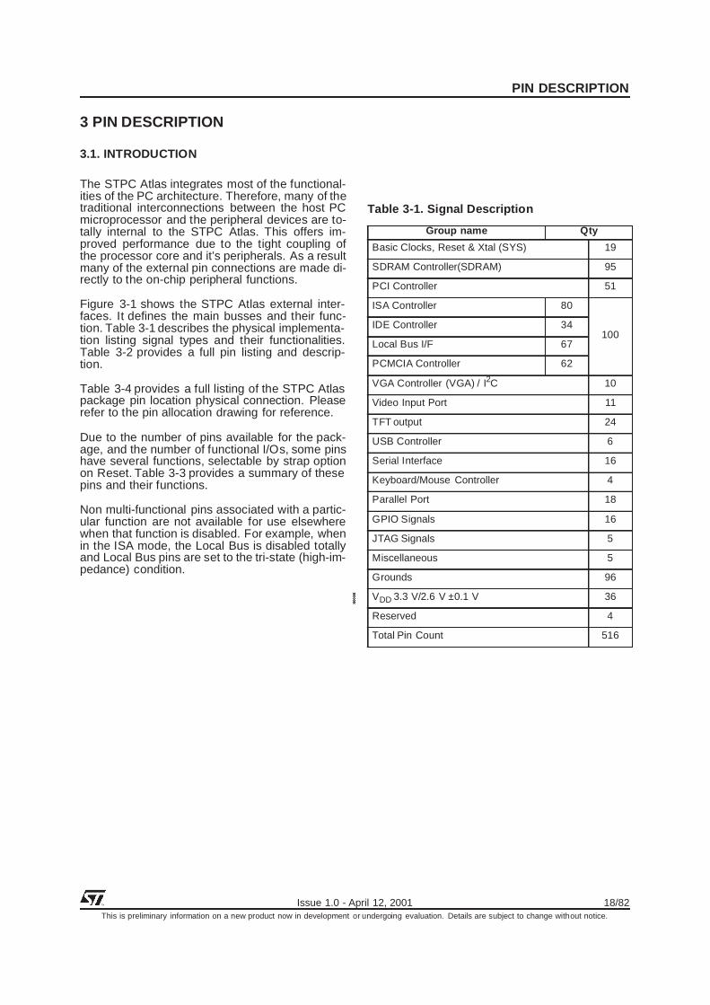
Figure 3-1 shows the STPC Atlas external inter-faces. It defines the main busses and their func-tion. Table 3-1 describes the physical implementa-tion listing signal types and their functionalities.Table 3-2 provides a full pin listing and descrip-tion.
Table 3-4 provides a full listing of the STPC Atlaspackage pin location physical connection. Pleaserefer to the pin allocation drawing for reference.
Due to the number of pins available for the pack-age, and the number of functional I/Os, some pinshave several functions, selectable by strap optionon Reset. Table 3-3 provides a summary of thesepins and their functions.
Non multi-functional pins associated with a partic-ular function are not available for use elsewherewhen that function is disabled. For example, whenin the ISA mode, the Local Bus is disabled totallyand Local Bus pins are set to the tri-state (high-im-pedance) condition.
Table 3-1. Signal Description
Group name Qty
Basic Clocks, Reset & Xtal (SYS) 19
SDRAM Controller(SDRAM) 95
PCI Controller 51
ISA Controller 80
100IDE Controller 34
Local Bus I/F 67
PCMCIA Controller 62
VGA Controller (VGA) / I2C 10
Video Input Port 11
TFT output 24
USB Controller 6
Serial Interface 16
Keyboard/Mouse Controller 4
Parallel Port 18
GPIO Signals 16
JTAG Signals 5
Miscellaneous 5
Grounds 96
VDD 3.3 V/2.6 V ±0.1 V 36
Reserved 4
Total Pin Count 516

PIN DESCRIPTION
19/82 Issue 1.0 - April 12, 2001This is preliminary information on a new product now in development or undergoing evaluation. Details are subject to change without notice.
Figure 3-1. STPC Atlas External Interfaces
Table 3-2. Definition of Signal Pins
Signal Name Dir Description Qty
BASIC CLOCKS AND RESETS
SYSRSTI#2 I System Reset / Power good 1
SYSRSTO#2 O Reset Output to System 1
XTALI I 14.3 MHz Crystal Input 1
XTALO O 14.3 MHz Crystal Output 1
PCI_CLKI2 I 33 MHz PCI Input Clock 1
PCI_CLKO O 33 MHz PCI Output Clock 1
ISA_CLK, ISA_CLK2X O ISA Clock x1 and x2 (also Multiplexer Select Line For IPC) 2
OSC14M2 O ISA bus synchronisation clock 1
HCLK2 I/O 100 / 133 MHz Host Clock (Test pin) 1
DEV_CLK2 O 48 MHz Peripheral Clock 1
DCLK2 I/O 135 MHz Dot Clock 1
VDD_xxx_PLL1 Power Supply for PLL Clocks (2.6 V ±0.1 V) 7
MEMORY CONTROLLER
MCLKI I Memory Clock Input 1
MCLKO O Memory Clock Output 1
Note1; These pins are must be connected to the 2.5 V + 0.2 V - 0.05 Vpower supply. They must not be connectedto the 3.3 V supply.
Note2; Denotes that the pin is V5T (see Section Table 4-1. )
Note 3; see Table 3-4 for V5T signals
PCI
x86 core
DRAM VGA TFT SYS I/O
95 10 24 11 51 19 100 16
STPC Atlas
PCMCIAISA/LOCAL BUS
NORTH BRIDGE SOUTH BRIDGE
VIPSignals

PIN DESCRIPTION
Issue 1.0 - April 12, 2001 20/82This is preliminary information on a new product now in development or undergoing evaluation. Details are subject to change without notice.
CS#[1:0] O DIMM Chip Select 2CS#[3]/MA[12]/BA[1] O DIMM Chip Select/ Memory Address/ Bank Address 1CS#[2]/MA[11] O DIMM Chip Select/ Bank Address 1BA[0] O Bank AddressMA[10:0] O Memory Row & Column Address 12
RAS#[1:0] O Row Address Strobe 2
CAS#[1:0] O Column Address Strobe 2
MWE# O Write Enable 1
MD[63:0]3 I/O Memory Data 64
CS#[3:0] O DIMM CHIP SELECT 4
DQM[7:0] O DATA INPUT/OUTPUT MASK 8
PCI INTERFACE
AD[31:0]2 I/O Address / Data 32
CBE[3:0]2 I/O Bus Commands / Byte Enables 4
FRAME#2 I/O Cycle Frame 1
TRDY#2 I/O Target Ready 1
IRDY#2 I/O Initiator Ready 1
STOP#2 I/O Stop Transaction 1
DEVSEL#2 I/O Device Select 1
PAR2 I/O Parity Signal Transactions 1
PERR# I/O Parity Error 1
SERR#2 O System Error 1
LOCK#2 I PCI Lock 1
PCI_REQ#[2:0]2 I PCI Request 3
PCI_GNT#[2:0]2 O PCI Grant 3
ISA BUS INTERFACE
LA[23:17]2 O Unlatched Address Bus 7
SA[19:0]2 O Latched Address Bus 20
SD[15:0]2 I/O Data Bus 16
IOCHRDY2 I I/O Channel Ready 1
ALE2 O Address Latch Enable 1
BHE#2 O System Bus High Enable 1
MEMR#2, MEMW#2 I/O Memory Read & Write 2
SMEMR#2, SMEMW#2 O System Memory Read and Write 2
Table 3-2. Definition of Signal Pins
Signal Name Dir Description Qty
Note1; These pins are must be connected to the 2.5 V + 0.2 V - 0.05 Vpower supply. They must not be connectedto the 3.3 V supply.
Note2; Denotes that the pin is V5T (see Section Table 4-1. )
Note 3; see Table 3-4 for V5T signals

PIN DESCRIPTION
21/82 Issue 1.0 - April 12, 2001This is preliminary information on a new product now in development or undergoing evaluation. Details are subject to change without notice.
IOR#2, IOW#2 I/O I/O Read and Write 2
MASTER#2 I Add On Card Owns Bus 1
MCS16#2, IOCS16#2 I Memory Chip Select 16, I/O Chip Select 16 2
REF#2 I Refresh Cycle 1
AEN2 O Address Enable 1
IOCHCK#2 I I/O Channel Check (ISA) 1
RTCRW#2 O RTC Read / Write# 1
RTCDS#2 O RTC Data Strobe 1
RTCAS#2 O RTC Address Strobe 1
RMRTCCS#2 O ROM / RTC Chip Select 1
GPIOCS#2 I/O General Purpose Chip Select 1
IRQ_MUX[3:0]2 I Multiplexed Interrupt Request 4
DACK_ENC[2:0]2 O DMA Acknowledge 3
DREQ_MUX[1:0]2 I Multiplexed DMA Request 2
TC2 O ISA Terminal Count 1
PCI_INT[3:0]2 I PCI Interrupt Request 4
ISAOE#2 I SELECT BETWEEN ISA OR IDE 1
KBCS#2 I/O KEYBOARD CHIP SELECT 1
ZWS#2 I ZERO WAIT STATE 1
IDE CONTROLLER
DD[15:0] I/O Data Bus 16
DA[2:0] O Address Bus 3
PCS3#/PCS1#/SCS3#/SCS1#
O Primary / secondary Chip Select 4
DIORDY O Data Io Ready 1
PIRQ2/SIRQ2 I Primary / Secondary Interupt Request 2
PDRQ2/SDRQ2 I Primary / Secondary Drive Drq 2
PDACK#2/SDACK#2 O Primary / Secondary Drive Dack 2
PDIOR#2/SDIOR#2 O Primary / Secondary IO Read 2
PDIOW#2/SDIOW#2 O Primary / Secondary IO Write 2
LOCAL BUS INTERFACE
PA[24:0]2 O Address Bus [24:0] 25
Table 3-2. Definition of Signal Pins
Signal Name Dir Description Qty
Note1; These pins are must be connected to the 2.5 V + 0.2 V - 0.05 Vpower supply. They must not be connectedto the 3.3 V supply.
Note2; Denotes that the pin is V5T (see Section Table 4-1. )
Note 3; see Table 3-4 for V5T signals

PIN DESCRIPTION
Issue 1.0 - April 12, 2001 22/82This is preliminary information on a new product now in development or undergoing evaluation. Details are subject to change without notice.
PD[15:0]2 I/O Data Bus [15:0] 16
PRD# O Peripheral Read Data 1
PRDY#2 I Ready 1
PWR#[1:0]2 O Memory and I/O Write signals 2
PRD#[1:0]2 O Memory and I/O Read signals 2
FCS#[1:0]2 O Flash Memory Chip Select 2
IOCS#[7:0]2 O I/O Chip Select 8
PBE#[1:0] O PERIPHERAL BYTE ENABLES 2
FCS_0H#2 O Bank 0 Upper Chip Select 1
FCS_0L#2 O Bank 0 Lower Chip Select 1
FCS_1H#2 O Bank 1 Upper Chip Select 1
FCS_1L#2 O Bank 1 Lower Chip Select 1
IRQ_MUX[3:0]1) I/O Muxed Interrupt Lines 4
PCMCIA INTERFACE
RESET O Reset 1
A O Address Bus 26
D I/O Data Bus 16
IORD#, IOWR# O I/O Read and Write 2
WP / IOIS16# I DMA Request // Write Protect // I/O Size is 16 bit 1
BVD2, BVD1 I Battery Voltage Detect 2
READY# / IREQ# I Busy / Ready# // Interrupt Request 1
WAIT# I Wait 1
OE# O Output Enable // DMA Terminal Count 1
WE# O Write Enable // DMA Terminal Count 1
REG# O DMA Acknowledge // Register 1
CD2#, CD1# I Card Detect 2
CE2#, CE1# O Card Enable 2
VCC5_EN O Power Switch control : 5 V power 1
VCC3_EN O Power Switch control : 3.3 V power 1
VPP_PGM O Power Switch control : Program power 1
VPP_VCC O Power Switch control : VCC power 1
GPI# I General Purpose Input 1
Table 3-2. Definition of Signal Pins
Signal Name Dir Description Qty
Note1; These pins are must be connected to the 2.5 V + 0.2 V - 0.05 Vpower supply. They must not be connectedto the 3.3 V supply.
Note2; Denotes that the pin is V5T (see Section Table 4-1. )
Note 3; see Table 3-4 for V5T signals

PIN DESCRIPTION
23/82 Issue 1.0 - April 12, 2001This is preliminary information on a new product now in development or undergoing evaluation. Details are subject to change without notice.
VGA CONTROLLER
RED, GREEN, BLUE O Red, Green, Blue 3
VSYNC2 I/O Vertical Sync 1
HSYNC2 I/O Horizontal Sync 1
VREF_DAC I DAC Voltage reference 1
RSET I Resistor Set 1
COMP I Compensation 1
DDC[1:0]2 I/O Display Data Channel Serial Link (See also SCL/SDA Signals) 2
DCLKOUT Display Dot Clock Out
VIDEO INPUT PORT
VCLK2 I/O 27-33 MHz VIDEO INPUT PORT CLOCK 1
VIN[7:0]2 I Video Input Data Bus 8
ODD_EVEN#2 I/O Video Input/TV Output Odd/even Field 1
VCS2 I/O Video Input/TV Output Horizontal Sync 1
TFT INTERFACE
R[5:0], G[5:0], B[5:0] O Red, Green, Blue 18
FPLINE O Horizontal Sync 1
FPFRAME O Vertical Sync 1
DE O Data Enable 1
ENAVDD O Enable Vdd of flat panel 1
ENVCC O Enable Vcc of flat panel 1
PWM O PWM back-light control 1
DCLOCK O Dot clock for Flat Panel 1
USB INTERFACE
OC I Over Current Detect 1
USBDPLS[0]1,USBDMNS[0]1
I/O Universal Serial Bus Data 0. 2
USBDPLS[1]1,USBDMNS[1]1
I/O Universal Serial Bus Port 1 2
POWERON2) O USB power supply lines 1
SERIAL CONTROLLER
CTS0#2, CTS1#2 I Clear to send, MSR[4] status bit 2
Table 3-2. Definition of Signal Pins
Signal Name Dir Description Qty
Note1; These pins are must be connected to the 2.5 V + 0.2 V - 0.05 Vpower supply. They must not be connectedto the 3.3 V supply.
Note2; Denotes that the pin is V5T (see Section Table 4-1. )
Note 3; see Table 3-4 for V5T signals

PIN DESCRIPTION
Issue 1.0 - April 12, 2001 24/82This is preliminary information on a new product now in development or undergoing evaluation. Details are subject to change without notice.
DCD0#2, DCD1#2 I Data Carrier detect, MSR[7] status bit 2
DSR0#2, DSR1#2 I Data set ready, MSR[5] status bit. 2
DTR0#, DTR1# O Data terminal ready, MSR[0] status bit 2
RI0#2, RI1# I Ring indicator, MSR[6] status bit 2
RTS0#, RTS1# O Request to send, MSR[1] status bit 2
RXD02, RXD12 I Receive data, Input Serial Input 2
TXD0, TXD1 O Transmit data, Serial Output 2
KEYBOARD & MOUSE INTERFACE
KBDATA2, MDATA2 I/O Keyboard & Mouse Data Line 2
KBCLK2, MCLK2 I/O Keyboard & Mouse Clock Line 2
PARALLEL PORT
PE2 I Paper End 1
SLCT2 I SELECT 1
BUSY#2 I BUSY 1
ERR#2 I ERROR 1
ACK#2 I Acknowledge 1
PDDIR#2 O Parallel Device Direction 1
STROBE#2 O PCS / STROBE# 1
INIT#2 O INIT 1
AUTPFDX#2 O Automatic Line Feed 1
SLCTIN#2 O SELECT IN 1
PPD[7:0]2 I/O Data Bus 8
I2C INTERFACE
SCL / DDC[1]2 I/O I C Interface - Clock / Can be used for VGA DDC[1] signal See VGA
SDA / DDC[0]2 I/O I C Interface - Data / Can be used for VGA DDC[0] signal See VGA
GPIO SIGNALS
GPIO[15:0]2 I/O General Purpose IOs 16
JTAG
TCLK2 I Test Clock 1
Table 3-2. Definition of Signal Pins
Signal Name Dir Description Qty
Note1; These pins are must be connected to the 2.5 V + 0.2 V - 0.05 Vpower supply. They must not be connectedto the 3.3 V supply.
Note2; Denotes that the pin is V5T (see Section Table 4-1. )
Note 3; see Table 3-4 for V5T signals

PIN DESCRIPTION
25/82 Issue 1.0 - April 12, 2001This is preliminary information on a new product now in development or undergoing evaluation. Details are subject to change without notice.
TRST2 I Test Reset 1
TDI2 I Test Data Input
TMS2 I Test Mode Set 1
TDO2 O Test Data output 1
MISCELLANEOUS
SCAN_ENABLE I Test Pin - Reserved 1
COL_SEL2 O Color Select 1
SPKRD2 O Speaker Device Output 1
Note 1.
Note 2.
Table 3-2. Definition of Signal Pins
Signal Name Dir Description Qty
Note1; These pins are must be connected to the 2.5 V + 0.2 V - 0.05 Vpower supply. They must not be connectedto the 3.3 V supply.
Note2; Denotes that the pin is V5T (see Section Table 4-1. )
Note 3; see Table 3-4 for V5T signals

PIN DESCRIPTION
Issue 1.0 - April 12, 2001 26/82This is preliminary information on a new product now in development or undergoing evaluation. Details are subject to change without notice.
3.2. SIGNAL DESCRIPTIONS
3.2.2 BASIC CLOCKS AND RESETS
SYSRSTI# System Reset/Power good. This inputis low when the reset switch is depressed. Other-wise, it reflects the power supply’s power goodsignal. PWGD is asynchronous to all clocks, andacts as a negative active reset. The reset circuitinitiates a hard reset on the rising edge of PWGD.
Note that while Reset is being asserted, the sig-nals on the device pins are in an unknown state.
SYSRSTO# Reset Output to System. This is thesystem reset signal and is used to reset the rest ofthe components (not on Host bus) in the system.The ISA bus reset is an externally inverted buff-ered version of this output and the PCI bus reset isan externally buffered version of this output.
XTALI 14.3 MHz Crystal InputXTALO 14.3 MHz Crystal Output.These pins arethe 14.318 MHz crystal input; This clock is used asthe reference clock for the internal frequency syn-thesizer to generate the HCLK and CLK24M.A 14.318 MHz series-cut Quartz Crystal should beconnected between these two pins. Balance ca-pacitors of 15 pF should also be added. In theevent of an external oscillator providing the masterclock signal to the STPC Atlas device, the TTL sig-nal should be provided on XTALO.
PCI_CLKI 33 MHz PCI Input Clock
This signal must be connected to a clock genera-tor and is usually connected to PCI_CLKO.
PCI_CLKO 33 MHz PCI Output Clock.This is themaster PCI bus clock output
ISA_CLK ISA Clock Output (also Multiplexer Se-lect Line For IPC). This pin produces the Clocksignal for the ISA bus. It is also used withISA_CLK2X as the multiplexor control lines for theInterrupt Controller Interrupt input lines. This is adivided down version of the PCICLK or OSC14M.
ISA_CLKX2 ISA Clock Output (also MultiplexerSelect Line For IPC).This pin produces a signal attwice the frequency of the ISA bus Clock signal. Itis also used with ISA_CLK as the multiplexor con-trol lines for the Interrupt Controller Interrupt inputlines.
CLK14M ISA bus synchronisation clock. This isthe buffered 14.318 MHz clock to the ISA bus.This clock also provides the reference clock to thefrequency synthesizer that generates GCLK2Xand DCLK.
HCLK Host Clock. This is the host 1X clock. Itsfrequency can vary from 50 to 75 MHz. All hosttransactions and PCI transactions are synchro-nized to this clock. Host transactions executed bythe DRAM controller are also driven by this clock.
DEV_CLK 24 MHz Peripheral Clock (floppydrive). This 24 MHz signal is provided as a con-venience for the system integration of a FloppyDisk driver function in an external chip.
DCLK 135 MHz Dot Clock. This is the dot clock,which drives graphics display cycles. Its frequencycan be as high as 135 MHz, and it is required tohave a worst case duty cycle of 60-40. For furtherdetails, refer to Section 3.1.3. bit 4.
3.2.3 MEMORY INTERFACE
MCLKI Memory Clock Input. This clock is drivingthe SDRAM controller, the graphics engine anddisplay controller. This input should be a bufferedversion of the MCLKO signal with the track lengthsbetween the buffer and the pin matched with thetrack lengths between the buffer and the MemoryBanks.
MCLKO Memory Clock Output.This clock drivesthe Memory Banks on board and is generatedfrom an internal PLL.
CS#[3]/MA[12]/BA[1] Chip Select/ Memory Ad-dress/ Bank AddressThis pin is CS#[3] in the casewhen 16 Mbit devices are used. For all other den-sities, it becomes MA[12] when 2 internal banksdevices are used and BA[1] when 4 internal bankdevices are used.
MA[10:0] Memory Address. Multiplexed row andcolumn address lines.
BA[0] Memory Bank Address.
CS#[1:0] Chip Select These signals are used todisable or enable device operation by masking orenabling all SDRAM inputs except MCLK, CKE,and DQM.
MD[63:0] Memory Data. This is the 64-bit memorydata bus. If only half of a bank is populated,MD63-32 is pulled high, data is on MD31-0.MD20-0 are also used as inputs at the rising edgeof PWGD to latch in power-up configuration infor-mation into the ADPC strap registers.
RAS#[1:0] Row Address Strobe. There are twoactive-low row address strobe output signals. TheRAS# signals drive the memory devices directlywithout any external buffering.
PIN DESCRIPTION
27/82 Issue 1.0 - April 12, 2001This is preliminary information on a new product now in development or undergoing evaluation. Details are subject to change without notice.
CAS#[1:0] Column Address Strobe. There aretwo active-low column address strobe output sig-nals. The CAS# signals drive the memory devicesdirectly without any external buffering.
MWE# Write Enable. Write enable specifieswhether the memory access is a read (MWE# = H)or a write (MWE# = L). This single write enablecontrols all DRAMs. It can be externally bufferedto boost the maximum number of loads (DRAMchips) supported.The MWE# signals drive the memory devices di-rectly without any external buffering.
3.2.4 PCI INTERFACE
AD[31:0] PCI Address/Data. This is the 32-bitmultiplexed address and data bus of the PCI. Thisbus is driven by the master during the addressphase and data phase of write transactions. It isdriven by the target during data phase of readtransactions.
PBE[3:0]# Bus Commands/Byte Enables. Theseare the multiplexed command and Byte enablesignals of the PCI bus. During the address phasethey define the command and during the dataphase they carry the Byte enable information.These pins are inputs when a PCI master otherthan the STPC Atlas owns the bus and outputswhen the STPC Atlas owns the bus.
FRAME# Cycle Frame. This is the frame signal ofthe PCI bus. It is an input when a PCI master ownsthe bus and is an output when STPC Atlas ownsthe PCI bus.
TRDY# Target Ready.This is the target ready sig-nal of the PCI bus. It is driven as an output whenthe STPC Atlas is the target of the current bustransaction. It is used as an input when STPC At-las initiates a cycle on the PCI bus.
IRDY# Initiator Ready. This is the initiator readysignal of the PCI bus. It is used as an output whenthe STPC Atlas initiates a bus cycle on the PCIbus. It is used as an input during the PCI cyclestargeted to the STPC Atlas to determine when thecurrent PCI master is ready to complete the cur-rent transaction.
STOP# Stop Transaction. STOP# is used to im-plement the disconnect, retry and abort protocol ofthe PCI bus. It is used as an input for the bus cy-cles initiated by the STPC Atlas and is used as anoutput when a PCI master cycle is targeted to theSTPC Atlas.
DEVSEL# Device Select. This signal is used asan input when the STPC Atlas initiates a bus cycleon the PCI bus to determine if a PCI slave devicehas decoded itself to be the target of the current
transaction. It is asserted as an output either whenthe STPC Atlas is the target of the current PCItransaction or when no other device asserts DEV-SEL# prior to the subtractive decode phase of thecurrent PCI transaction.
PAR Parity Signal Transactions.This is the paritysignal of the PCI bus. This signal is used to guar-antee even parity across AD[31:0], CBE[3:0]#,and PAR. This signal is driven by the master dur-ing the address phase and data phase of writetransactions. It is driven by the target during dataphase of read transactions. (Its assertion is identi-cal to that of the AD bus delayed by one PCI clockcycle)
PERR# Parity Error
SERR# System Error. This is the system error sig-nal of the PCI bus. It may, if enabled, be assertedfor one PCI clock cycle if target aborts a STPC At-las initiated PCI transaction. Its assertion by eitherthe STPC Atlas or by another PCI bus agent willtrigger the assertion of NMI to the host CPU. Thisis an open drain output.
LOCK# PCI Lock. This is the lock signal of the PCIbus and is used to implement the exclusive busoperations when acting as a PCI target agent.
PCI_REQ#[2:0] PCI Request. These pins are thethree external PCI master request pins. They indi-cates to the PCI arbiter that the external agentsdesire use of the bus.
PCI_GNT#[2:0] PCI Grant. These pins indicatethat the PCI bus has been granted to the masterrequesting it on its PCI_REQ#.
PCI_INT[3:0] PCI Interrupt Request. These arethe PCI bus interrupt signals. They are to be en-coded before connection to the STPC Atlas usingISACLK and ISACLKX2 as the input selectionstrobes.
3.2.5 LOCAL BUS
PA[24:0] Address Bus Output.
PD[15:0] Data Bus. This is the 16-bit data bus.D[7:0] is the LSB and PD[15:8] is the MSB.
PWR#[1:0] Write Control output.These are mem-ory and I/O Write signals. PWR0# is used to writethe LSB and PWR1# to write the MSB.
PRD#[1:0] Read Control output. These are mem-ory and I/O Read signals. PWR0# is used to readthe LSB and PWR1# to read the MSB.

PIN DESCRIPTION
Issue 1.0 - April 12, 2001 28/82This is preliminary information on a new product now in development or undergoing evaluation. Details are subject to change without notice.
PRDY# Data Ready input. This signal is used tocreate wait states on the bus. When low, it com-pletes the current cycle.
FCS#[3:0] Four Flash Memory Chip Select out-puts. These are the Programmable Chip Selectsignals for up to 4 banks of Flash memory (Banks0 and 1, Upper and Lower).
IOCS#[7:0] I/O Chip Select output.These are theProgrammable Chip Select signals for up to 4 ex-ternal I/O devices.
IRQ_MUX#[3:0] Multiplexed Interrupt Lines.
3.2.6 ISA BUS INTERFACE
LA[23:17] Unlatched Address. These unlatchedISA Bus pins address bits 23-17 on 16-bit devices.When the ISA bus is accessed by any cycle initiat-ed from the PCI bus, these pins are in outputmode. When an ISA bus master owns the bus,these pins are tristated.
SA[19:0] Unlatched Address. These are the 20low bits of the system address bus of ISA. Thesepins are used as an input when an ISA bus masterowns the bus and are outputs at all other times.
SD[15:0] I/O Data Bus (ISA). These are the exter-nal ISA databus pins.
IOCHRDY IO Channel Ready. IOCHRDY is the IOchannel ready signal of the ISA bus and is drivenas an output in response to an ISA master cycletargeted to the host bus or an internal register ofthe STPC Atlas. The STPC Atlas monitors this sig-nal as an input when performing an ISA cycle onbehalf of the host CPU, DMA master or refresh.ISA masters which do not monitor IOCHRDY arenot guaranteed to work with the STPC Atlas sincethe access to the system memory can be consid-erably delayed due to CRT refresh or a write backcycle.
ALE Address Latch Enable. This is the addresslatch enable output of the ISA bus and is assertedby the STPC Atlas to indicate that LA23-17, SA19-0, AEN and SBHE# signals are valid. The ALE isdriven high during refresh, DMA master or an ISAmaster cycles by the STPC Atlas.ALE is driven low after reset.
BHE# System Bus High Enable.This signal, whenasserted, indicates that a data Byte is being trans-ferred on SD15-8 lines. It is used as an input whenan ISA master owns the bus and is an output at allother times.
MEMR# Memory Read. This is the memory readcommand signal of the ISA bus. It is used as an in-put when an ISA master owns the bus and is an
output at all other times.The MEMR# signal is active during refresh.
MEMW# Memory Write. This is the memory writecommand signal of the ISA bus. It is used as an in-put when an ISA master owns the bus and is anoutput at all other times.
SMEMR# System Memory Read.The STPC Atlasgenerates SMEMR# signal of the ISA bus onlywhen the address is below one MByte or the cycleis a refresh cycle.
SMEMW# System Memory Write. The STPC At-las generates SMEMW# signal of the ISA bus onlywhen the address is below one MByte.
IOR# I/O Read. This is the IO read command sig-nal of the ISA bus. It is an input when an ISA mas-ter owns the bus and is an output at all othertimes.
IOW# I/O Write. This is the IO write command sig-nal of the ISA bus. It is an input when an ISA mas-ter owns the bus and is an output at all othertimes.
MASTER# Add On Card Owns Bus.This signal isactive when an ISA device has been granted busownership.
MCS16# Memory Chip Select16. This is the de-code of LA23-17 address pins of the ISA addressbus without any qualification of the command sig-nal lines. MCS16# is always an input. The STPCAtlas ignores this signal during IO and refresh cy-cles.
IOCS16# IO Chip Select16. This signal is the de-code of SA15-0 address pins of the ISA addressbus without any qualification of the command sig-nals. The STPC Atlas does not drive IOCS16#(similar to PC-AT design). An ISA master accessto an internal register of the STPC Atlas is execut-ed as an extended 8-bit IO cycle.
REF# Refresh Cycle.This is the refresh commandsignal of the ISA bus. It is driven as an outputwhen the STPC Atlas performs a refresh cycle onthe ISA bus. It is used as an input when an ISAmaster owns the bus and is used to trigger a re-fresh cycle.The STPC Atlas performs a pseudo hidden re-fresh. It requests the host bus for two host clocksto drive the refresh address and capture it in exter-nal buffers. The host bus is then relinquishedwhile the refresh cycle continues on the ISA bus.
AEN Address Enable. Address Enable is enabledwhen the DMA controller is the bus owner to indi-cate that a DMA transfer will occur. The enabling

PIN DESCRIPTION
29/82 Issue 1.0 - April 12, 2001This is preliminary information on a new product now in development or undergoing evaluation. Details are subject to change without notice.
of the signal indicates to IO devices to ignore theIOR#/IOW# signal during DMA transfers.
IOCHCK# IO Channel Check. IO Channel Checkis enabled by any ISA device to signal an errorcondition that can not be corrected. NMI signal be-comes active upon seeing IOCHCK# active if thecorresponding bit in Port B is enabled.
GPIOCS# I/O General Purpose Chip Select 1.This output signal is used by the external latch onISA bus to latch the data on the SD[7:0] bus. Thelatch can be use by PMU unit to control the exter-nal peripheral devices to power down or any otherdesired function.This pin is also serves as a strap input during re-set.
RTCRW# Real Time Clock RW#. This pin is usedas RTCRW#. This signal is asserted for any I/Owrite to port 71h.
RTCDS# Real Time Clock DS. This pin is used asRTCDS. This signal is asserted for any I/O read toport 71h.
RTCAS# Real time clock address strobe.This sig-nal is asserted for any I/O write to port 70h.
RMRTCCS# ROM/Real Time clock chip select.This pin is a multi-function pin. This signal is as-serted if a ROM access is decoded during a mem-ory cycle. It should be combined with MEMR# orMEMW# signals to properly access the ROM.During an IO cycle, this signal is asserted if ac-cess to the Real Time Clock (RTC) is decoded. Itshould be combined with IOR# or IOW# signals toproperly access the real time clock.
IRQ_MUX[3:0] Multiplexed Interrupt Request.These are the ISA bus interrupt signals. They areto be encoded before connection to the STPC At-las using ISACLK and ISACLKX2 as the input se-lection strobes.Note that IRQ8B, which by convention is connect-ed to the RTC, is inverted before being sent to theinterrupt controller, so that it may be connected di-rectly to the IRQ# pin of the RTC.
ISAOE# Bidirectional OE Control.This signal con-trols the OE signal of the external transceiver thatconnects the IDE DD bus and ISA SA bus.
KBCS# Keyboard Chip Select. This signal is as-serted if a keyboard access is decoded during a I/O cycle.
ZWS# Zero Wait State. This signal, when assert-ed by addressed device, indicates that current cy-cle can be shortened.
DACK_ENC[2:0] DMA Acknowledge. These arethe ISA bus DMA acknowledge signals. They areencoded by the STPC Atlas before output andshould be decoded externally using ISACLK andISACLKX2 as the control strobes.
DREQ_MUX[1:0] ISA Bus Multiplexed DMA Re-quest. These are the ISA bus DMA request sig-nals. They are to be encoded before connection tothe STPC Atlas using ISACLK and ISACLKX2 asthe input selection strobes.
TC ISA Terminal Count. This is the terminal countoutput of the DMA controller and is connected tothe TC line of the ISA bus. It is asserted during thelast DMA transfer, when the Byte count expires.
3.2.7 PCMCIA INTERFACE
RESET Card Reset. This output forces a hardreset to a PC Card.
A[25:0] Address Bus. These are the 25 low bits ofthe system address bus of the PCMCIA bus.These pins are used as an input when an PCMCIAbus owns the bus and are outputs at all othertimes.
D[15:0] I/O Data Bus (PCMCIA). These are theexternal PCMCIA databus pins.
IORD# I/O Read. This output is used with REG# togate I/O read data from the PC Card, (only whenREG# is asserted).
IOWR# I/O Write. This output is used with REG#to gate I/O write data from the PC Card, (onlywhen REG# is asserted).
WP Write Protect. This input indicates the statusof the Write Protect switch (if fitted) on memory PCCards (asserted when the switch is set to writeprotect).
BVD1, BVD2 Battery Voltage Detect. These in-puts will be generated by memory PC Cards thatinclude batteries and are an indication of the con-dition of the batteries. BVD1 and BVD2 are keptasserted high when the battery is in good condi-tion.
READY#/BUSY#/IREQ# Ready/busy/Interupt re-quest. This input is driven low by memory PCCards to signal that their circuits are busyprocessing a previous write command.
WAIT# Bus Cycle Wait.This input is driven by thePC Card to delay completion of the memory or I/Ocycle in progress.
OE# Output Enable. OE# is an active low outputwhich is driven to the PC Card to gate MemoryRead data from memory PC Cards.

PIN DESCRIPTION
Issue 1.0 - April 12, 2001 30/82This is preliminary information on a new product now in development or undergoing evaluation. Details are subject to change without notice.
WE#/PRGM# Write Enable. This output is used bythe host for gating Memory Write data. WE# isalso used for memory PC Cards that have pro-grammable memory.
REG# Attribute Memory Select. This output is in-active (high) for all normal accesses to the MainMemory of the PC Card. I/O PC Cards will only re-spond to IORD# or IOWR# when REG# is active(low). Also see Section 3.2.10
CD1#, CD2# Card Detect. These inputs providefor the detection of correct card insertion. CD#1and CD#2 are positioned at opposite ends of theconnector to assist in the detection process.These inputs are internally grounded on the PCCard therefore they will be forced low whenever acard is inserted in a socket.
CE1#, CE2# Card Enable. These are active lowoutput signals provided from the PCIC. CE#1 ena-bles even Bytes, CE#2 odd Bytes.
ENABLE# Enable. This output is used to activate/select a PC Card socket. ENABLE# controls theexternal address buffer logic.C card has been de-tected (CD#1 and CD#2 = ’0’).
ENIF# ENIF. This output is used to activate/selecta PC Card socket.
EXT_DIR EXternal Transreceiver Direction Con-trol. This output is high during a read and low dur-ing a write. The default power up condition is write(low). Used for both Low and High Bytes of theData Bus.
VCC_EN#, VPP1_EN0, VPP1_EN1, VPP 2_EN0,VPP2_EN1 Power Control. Five output signalsused to control voltages (VPP1, VPP2 and VCC)to a PC Card socket. Also seeSection 13.7.5.
GPI# General Purpose Input. This signal is hard-wired to 1.
3.2.8 IDE INTERFACE
DA[2:0] Address. These signals are connected toDA[2:0] of IDE devices directly or through a buffer.If the toggling of signals are to be masked duringISA bus cycles, they can be externally ORed withISAOE# before being connected to the IDE devic-es.
DD[15:0] Databus. When the IDE bus is active,they serve as IDE signals DD[11:0]. IDE devicesare connected to SA[19:8] directly and ISA bus isconnected to these pins through two LS245 trans-ceivers.
PCS1#, PCS3# Primary Chip Select. These sig-nals are used as the active high primary master &
slave IDE chip select signals. These signals mustbe externally ANDed with the ISAOE# signal be-fore driving the IDE devices to guarantee it is ac-tive only when ISA bus is idle.
SCS1#, SCS3# Secondary Chip Select. Thesesignals are used as the active high secondarymaster & slave IDE chip select signals. These sig-nals must be externally ANDed with the ISAOE#signal before driving the IDE devices to guaranteeit is active only when ISA bus is idle.
DIORDY Busy/Ready. This pin serves as IDE sig-nal DIORDY.
PIRQ Primary Interrupt Request.SIRQ Secondary Interrupt Request.Interrupt request from IDE channels.
PDRQ Primary DMA Request.SDRQ Secondary DMA Request.DMA request from IDE channels.
PDACK# Primary DMA Acknowledge.SDACK# Secondary DMA Acknowledge.DMA acknoledge to IDE channels.
PDIOR#, PDIOW# Primary I/O Read & Write.SDIOR#, SDIOW# Secondary I/O Read & Write.Primary & Secondary channel read & write.Monitor Interface
3.2.9 USB Interface
OC OVER CURRENT DETECT This signal isused to monitor the status of the USB power sup-ply lines of both devices. USB port are disabledwhen OC signal is asserted.
USBDPL0, USBDMNS0 UNIVERSAL SERIALBUS DATA 0 This signal pair comprises the differ-ential data signal for USB port 0.
USBDPL1, USBDMNS1 UNIVERSAL SERIALBUS PORT 1 This signal pair comprises the differ-ential data signal for USB port 1.
POWERON USB power supply lines

PIN DESCRIPTION
31/82 Issue 1.0 - April 12, 2001This is preliminary information on a new product now in development or undergoing evaluation. Details are subject to change without notice.
3.2.10 IPC
DACK_ENC[2:0] DMA Acknowledge. These arethe ISA bus DMA acknowledge signals. They areencoded by the STPC Industrial before output andshould be decoded externally using ISACLK andISACLKX2 as the control strobes.
DREQ_MUX[1:0] ISA Bus Multiplexed DMA Re-quest. These are the ISA bus DMA request sig-nals. They are to be encoded before connection tothe STPC Industrial using ISACLK and ISACLKX2as the input selection strobes.
TC ISA Terminal Count. This is the terminal countoutput of the DMA controller and is connected tothe TC line of the ISA bus. It is asserted during thelast DMA transfer, when the Byte count expires.
3.2.11 KEYBOARD/MOUSE INTERFACE
KBCLK, Keyboard Clock line. Keyboard data islatched by the controller on each negative clockedge produced on this pin. The keyboard can bedisabled by pulling this pin low by software control.
KBDATA, Keyboard Data Line.11-bits of data areshifted serially through this line when data is beingtransferred. Data is synchronised to KBCLK.
MCLK, Mouse Clock line. Mouse data is latchedby the controller on each negative clock edge pro-duced on this pin. The mouse can be disabled bypulling this pin low by software control.
MDATA, Mouse Data Line. 11-bits of data areshifted serially through this line when data is beingtransferred. Data is synchronised to MCLK.
3.2.12 SERIAL INTERFACE
RXD0, RXD1 Serial Input.Data is clocked in usingRCLK/16.
TXD0, TXD1 Serial Output. Data is clocked outusing TCLK/16 (TCLK=BAUD#).
DCD0#, DCD1# Input Data carrier detect.
RI0#, RI1# Input Ring indicator.
DSR0#, DSR1# Input Data set ready.
CTS0#, CTS1# Input Clear to send.
RTS0#, RTS1# Output Request to send.
DTR0#, DTR1# Output Data terminal read.
3.2.13 PARALLEL PORT
PE Paper End. Input status signal from printer.
SLCT Printer Select. Printer selected input.
BUSY# Printer Busy.Input status signal from printer.
ERR# Error. Input status signal from printer.
ACK# Acknowledge.Input status signal from printer.
PDDIR# Parallel Device Direction.Bidirectional control line output.
STROBE# PCS/Strobe#.Data transfer strobe line to printer.
INIT# Initialize Printer.This output sends an initial-ize command to the connected printer.
AUTPFDX# Automatic Line feed. This outputsends a command to the connected printer to au-tomatically generate line feed on received car-riage returns.
SLCTIN# Select In. Printer select output.
PPD[7-0] Printer Data Lines Data transfer lines toprinter. Bidirectional depending on modes.
3.2.14 PCMCIA INTERFACE
RESET Card Reset. This output forces a hardreset to a PC Card.
A[25:0] Address Bus. These are the 25 low bits ofthe system address bus of the PCMCIA bus.These pins are used as an input when an PCMCIAbus owns the bus and are outputs at all othertimes.
D[15:0] I/O Data Bus (PCMCIA). These are theexternal PCMCIA databus pins.
IORD# I/O Read. This output is used with REG# togate I/O read data from the PC Card, (only whenREG# is asserted).
IOWR# I/O Write. This output is used with REG#to gate I/O write data from the PC Card, (onlywhen REG# is asserted).
WP Write Protect. This input indicates the statusof the Write Protect switch (if fitted) on memory PCCards (asserted when the switch is set to writeprotect).
BVD1, BVD2 Battery Voltage Detect. These in-puts will be generated by memory PC Cards that

PIN DESCRIPTION
Issue 1.0 - April 12, 2001 32/82This is preliminary information on a new product now in development or undergoing evaluation. Details are subject to change without notice.
include batteries and are an indication of the con-dition of the batteries. BVD1 and BVD2 are keptasserted high when the battery is in good condi-tion.
READY#/BUSY#/IREQ# Ready/busy/Interupt re-quest. This input is driven low by memory PCCards to signal that their circuits are busyprocessing a previous write command.
WAIT# Bus Cycle Wait. This input is driven by thePC Card to delay completion of the memory or I/Ocycle in progress.
OE# Output Enable. OE# is an active low outputwhich is driven to the PC Card to gate MemoryRead data from memory PC Cards.
WE#/PRGM# Write Enable. This output is used bythe host for gating Memory Write data. WE# isalso used for memory PC Cards that have pro-grammable memory.
REG# Attribute Memory Select. This output is in-active (high) for all normal accesses to the MainMemory of the PC Card. I/O PC Cards will only re-spond to IORD# or IOWR# when REG# is active(low). Also see Section 3.2.10
CD1#, CD2# Card Detect. These inputs providefor the detection of correct card insertion. CD#1and CD#2 are positioned at opposite ends of theconnector to assist in the detection process.These inputs are internally grounded on the PCCard therefore they will be forced low whenever acard is inserted in a socket.
CE1#, CE2# Card Enable. These are active lowoutput signals provided from the PCIC. CE#1 ena-bles even Bytes, CE#2 odd Bytes.
ENABLE# Enable. This output is used to activate/select a PC Card socket. ENABLE# controls theexternal address buffer logic.C card has been de-tected (CD#1 and CD#2 = ’0’).
ENIF# ENIF. This output is used to activate/selecta PC Card socket.
EXT_DIR EXternal Transreceiver Direction Con-trol. This output is high during a read and low dur-ing a write. The default power up condition is write(low). Used for both Low and High Bytes of theData Bus.
VCC_EN#, VPP1_EN0, VPP1_EN1, VPP 2_EN0,VPP2_EN1 Power Control. Five output signalsused to control voltages (VPP1, VPP2 and VCC)to a PC Card socket. Also seeSection 13.7.5.
GPI# General Purpose Input. This signal is hard-wired to 1.
3.2.15 MONITOR INTERFACE
RED, GREEN, BLUE RGB Video Outputs.Theseare the 3 analog color outputs from the RAM-DACs. These signals are sensitive to interference,therefore they need to be properly shielded.
VSYNC Vertical Synchronisation Pulse. This isthe vertical synchronization signal from the VGAcontroller.
HSYNC Horizontal Synchronisation Pulse.This isthe horizontal synchronization signal from theVGA controller.
VREF_DAC DAC Voltage reference. This pin isan input driving the digital to analog converters.This allows an external voltage reference sourceto be used.
RSET Resistor Current Set.This is the referencecurrent input to the RAMDAC. Used to set the full-scale output of the RAMDAC.
COMP Compensation. This is the RAMDAC com-pensation pin. Normally, an external capacitor(typically 10nF) is connected between this pin andVDD to damp oscillations.
DDC[1:0] Direct Data Channel Serial Link.Thesebidirectional pins are connected to CRTC register3Fh to implement DDC capabilities. They conformto I2C electrical specifications, they have open-collector output drivers which are internally con-nected to VDD through pull-up resistors.
They can instead be used for accessing I C devic-es on board. DDC1 and DDC0 correspond to SCLand SDA respectively.
3.2.16 VIDEO INTERFACE
VCLK Pixel Clock Input.This signal is used to syn-chronise data being transfered from an externalvideo device to either the frame buffer, or alterna-tively out the TV output in bypass mode. This pincan be sourced from STPC if no external VCLK isdetected, or can be input from an external videoclock source.
VIN[7:0] YUV Video Data Input ITU-R 601 or 656.Time multiplexed 4:2:2 luminance and chromi-nance data as defined in ITU-R Rec601-2 andRec656 (except for TTL input levels). This bustypically carries a stream of Cb,Y,Cr,Y digital vid-eo at VCLK frequency, clocked on the rising edge(by default) of VCLK.
PIN DESCRIPTION
33/82 Issue 1.0 - April 12, 2001This is preliminary information on a new product now in development or undergoing evaluation. Details are subject to change without notice.
3.2.17 TFT INTERFACE SIGNALS
The TFT (Thin Film Transistor) interface convertssignals from the CRT controller into control signalsfor an external TFT Flat Panel. The signals arelisted below.
TFTFRAME, Vertical Sync. pulse Output.
TFTLINE, Horizontal Sync. Pulse Output.
TFTDE, Data Enable.
TFTR5-0, Red Output.
TFTG5-0, Green Output.
TFTB5-0, Blue Output.
TFTENVDD, Enable VDD of Flat Panel.
TFTENVCC, Enable VCC of Flat Panel.
PWM PWM Back-Light Control.
TFTDCLOCK, Dot clock for the Flat Panel.
3.2.18 MISCELLANEOUS
SPKRD Speaker Drive. This is the output to thespeaker and is the AND of the counter 2 outputwith bit 1 of Port 61h and drives an external speak-er driver. This output should be connected to a7407 type high voltage driver.
SCAN_ENABLE Reserved. This pin is reservedfor Test and Miscellaneous functions. It has to beset to ‘0’ or connected to ground in normal opera-tion.
COL_SEL Colour Select. Can be used for Picturein Picture function. Note however that this signal,brought out from the video pipeline, is not in syncwith the VGA output signals, i.e. the VGA signalsrun four clock cycles after the Col_Sel signal.

PIN DESCRIPTION
Issue 1.0 - April 12, 2001 34/82This is preliminary information on a new product now in development or undergoing evaluation. Details are subject to change without notice.
3.1. SIGNAL DETAIL
The muxing between ISA, LOCAL BUS and PCM-CIA is performed by external strap options. The
resulting interface is then dynamically muxed withthe UIDE Interface.
Table 3-3. Signals multiplexing on the same pin
ISA Pin Name IDE Pin Name Local Bus Pin Name PCMCIA Pin Names
SA[19:8] DD[11:0] A[19:8]
SA[7:0] PA[7:4],PRDY, IOCS#[2:0] A[7:0]
SD[15:0] PD[15:0] D[15:0]
LA[23:20]SCS3#,SCS1#,PCS3#,PCS1#
A[23:20]
LA[19:17] DA[2:0] Not used,A[25:24]
IOCHRDY DIORDY
RMRTCCS#, RTCAS,RTCRW#, RTCDS
DD[15:12]
BHE# PA[17] OE#
ALE PA[15]
AEN PA[16] WAIT#
MEMR# PA[14]
MEMW# PA[18]
SMEMR# PA[19] VCC3_EN
SMEMW# PBE#[1] VPP_PGM
IOR# PA[13] IORD#
IOW# PA[12] IOWR#
MASTER# PRD# BVD1
MCS16# PWR#
IOCS16# PBE#[0] WP/IOIS16#
REF# PA[11] RESET
IOCHCK# PA[10] BVD2
GPIOCS# PA[9] VCC5_EN
ZWS# PA[8] GPI#
ISAOE# ISAOE# IOCS#[3]
DREQ_MU#[1:0] PA[21:20] CE2#, CE1#
DACK_ENC [2:0] PA[2:0]
TC PA[3]
PA[23] VPP_VCC
PA[24] WE#
IOCS#[7] REG#
IOCS#[6] READY#
IOCS#[5] CD1#
IOCS#[4] CD2#

PIN DESCRIPTION
35/82 Issue 1.0 - April 12, 2001This is preliminary information on a new product now in development or undergoing evaluation. Details are subject to change without notice.
Table 3-4. Pinout
Pin# Pin Name
D15 SYSRSETI#
C15 SYSRSETO#
AF21 XTALI
AF22 XTALO
AF23 PCI_CLKI
AF24 PCI_CLKO
E15 ISA_CLK
A16 ISA_CLK2X
AB18 OSC14M
AB24 HCLK
AB25 DEV_CLK
AC18 DCLK
AF20 MCLKI
AF19 MCLKO
U5 MA[0]
V1 MA[1]
V2 MA[2]
V3 MA[3]
V4 MA[4]
V5 MA[5]
W1 MA[6]
W2 MA[7]
W3 MA[8]
W5 MA[9]
Y1 MA[10]
Y2 MA[11]
U3 RAS#[0]
U4 RAS#[1]
R5 CAS#[0]
T1 CAS#[1]
R4 MWE#
J4 MD[0]
J2 MD[1]
Note1; This signal is multiplexedsee Table 3-3
K5 MD[2]
K3 MD[3]
K1 MD[4]
L4 MD[5]
L2 MD[6]
M5 MD[7]
M3 MD[8]
M1 MD[9]
N4 MD[10]
N2 MD[11]
P1 MD[12]
P3 MD[13]
P5 MD[14]
R2 MD[15]
AA4 MD[16]
AB1 MD[17]
AB3 MD[18]
AC1 MD[19]
AC3 MD[20]
AD2 MD[21]
AF3 MD[22]
AE4 MD[23]
AF4 MD[24]
AD5 MD[25]
AF5 MD[26]
AC6 MD[27]
AF6 MD[28]
AC7 MD[29]
AE7 MD[30]
AB8 MD[31]
J3 MD[32]
J1 MD[33]
K4 MD[34]
K2 MD[35]
L5 MD[36]
Table 3-4. Pinout
Pin# Pin Name
Note1; This signal is multiplexedsee Table 3-3
L3 MD[37]
L1 MD[38]
M4 MD[39]
M2 MD[40]
N5 MD[41]
N3 MD[42]
N1 MD[43]
P2 MD[44]
P4 MD[45]
R1 MD[46]
R3 MD[47]
AA5 MD[48]
AB2 MD[49]
AB4 MD[50]
AC2 MD[51]
AD1 MD[52]
AE3 MD[53]
AD4 MD[54]
AC5 MD[55]
AB6 MD[56]
AE5 MD[57]
AB7 MD[58]
AD6 MD[59]
AE6 MD[60]
AD7 MD[61]
AF7 MD[62]
AC8 MD[63]
U1 CS#[0]
U2 CS#[1]
Y3 CS#[2]
Y4 CS#[3]/MA[12]/BA[1]
T2 DQM[0]
T4 DQM[1]
Y5 DQM[2]
AA2 DQM[3]
Table 3-4. Pinout
Pin# Pin Name
Note1; This signal is multiplexedsee Table 3-3
PIN DESCRIPTION
Issue 1.0 - April 12, 2001 36/82This is preliminary information on a new product now in development or undergoing evaluation. Details are subject to change without notice.
T3 DQM[4]
T5 DQM[5]
AA1 DQM[6]
AA3 DQM[7]
B3 AD[0]
A3 AD[1]
C4 AD[2]
B4 AD[3]
A4 AD[4]
D5 AD[5]
C5 AD[6]
B5 AD[7]
A5 AD[8]
D6 AD[9]
C6 AD[10]
B6 AD[11]
A6 AD[12]
E7 AD[13]
D7 AD[14]
C7 AD[15]
A9 AD[16]
E10 AD[17]
C10 AD[18]
B10 AD[19]
A10 AD[20]
E11 AD[21]
D11 AD[22]
C11 AD[23]
A11 AD[24]
E12 AD[25]
D12 AD[26]
C12 AD[27]
B12 AD[28]
A12 AD[29]
Table 3-4. Pinout
Pin# Pin Name
Note1; This signal is multiplexedsee Table 3-3
E13 AD[30]
D13 AD[31]
E6 CBE[0]
B7 CBE[1]
B9 CBE[2]
B11 CBE[3]
C9 FRAME#
E9 TRDY#
D9 IRDY#
B8 STOP#
A8 DEVSEL#
A7 PAR
D8 PERR#
E8 SERR#
C8 LOCK#
C14 PCI_REQ#[0]
B14 PCI_REQ#[1]
A14 PCI_REQ#[2]
A13 PCI_GNT#[0]
B13 PCI_GNT#[1]
C13 PCI_GNT#[2]
C20 LA[17]1
B21 LA[18]1
B20 LA[19]1
E19 LA[20]1
E18 LA[21]1
C21 LA[22]1
D19 LA[23]1
P22 SA[0]1
P23 SA[1]1
P24 SA[2]1
P25 SA[3]1
P26 SA[4]1
N26 SA[5]1
Table 3-4. Pinout
Pin# Pin Name
Note1; This signal is multiplexedsee Table 3-3
N25 SA[6]1
N24 SA[7]1
N23 SA[8]1
N22 SA[9]1
M26 SA[10]1
M25 SA[11]1
M24 SA[12]1
M23 SA[13]1
M22 SA[14]1
L26 SA[15]1
L25 SA[16]1
L24 SA[17]1
L23 SA[18]1
L22 SA[19]1
K24 SD[0]1
J26 SD[1]1
J25 SD[2]1
J24 SD[3]1
K23 SD[4]1
K22 SD[5]1
H26 SD[6]1
H25 SD[7]1
H24 SD[8]1
G26 SD[9]1
G25 SD[10]1
G24 SD[11]1
J22 SD[12]1
J23 SD[13]1
F26 SD[14]1
F25 SD[15]1
F23 IOCHRDY1
D20 ALE1
K25 BHE#1
F24 MEMR#1
A22 MEMW#1
Table 3-4. Pinout
Pin# Pin Name
Note1; This signal is multiplexedsee Table 3-3

PIN DESCRIPTION
37/82 Issue 1.0 - April 12, 2001This is preliminary information on a new product now in development or undergoing evaluation. Details are subject to change without notice.
G23 SMEMR#1
E21 SMEMW#1
H22 IOR#1
E26 IOW#1
E25 MASTER#1
E24 MCS16#1
C22 IOCS16#1
G22 REF#1
E17 AEN1
A23 IOCHCK#1
U25 RTCRW#1
U26 RTCDS1
U24 RTCAS1
U23 RMRTCCS#1
D22 GPIOCS#1
D24 IRQ_MUX[0]
E23 IRQ_MUX[1]
C26 IRQ_MUX[2]
F22 IRQ_MUX[3]
A24 DACK_ENC[0]
C23 DACK_ENC[1]1
B23 DACK_ENC[2]1
D26 DREQ_MUX[0]1
D25 DREQ_MUX[1]1
B24 TC1
B15 PCI_INT[0]
A15 PCI_INT[1]
E14 PCI_INT[2]
D14 PCI_INT[3]
B16 ISAOE#1
B22 KBCS#
K26 ZWS#1
R23 PIRQ
R24 SIRQ
Table 3-4. Pinout
Pin# Pin Name
Note1; This signal is multiplexedsee Table 3-3
T22 PDRQ
T23 SDRQ
R25 PDACK#
R26 SDACK#
T25 PDIOR#
T24 PDIOW#
R22 SDIOR#
T26 SDIOW#
D18 PA[22]
C19 PA[23]
B19 PA[24]
A17 FCS_0H
B17 FCS_0L
C16 FCS_1H
E16 FCS_1L
D17 IOCS#[4]
C18 IOCS#[5]
B18 IOCS#[6]
C17 IOCS#[7]
AD8 RED
AF8 GREEN
AC9 BLUE
AB10 VSYNC
AF9 HSYNC
AB9 VREF_DAC
AD9 RSET
AE8 COMP
AB15 VCLK
AF16 VIN[0]
AE16 VIN[1]
AC16 VIN[2]
AB16 VIN[3]
Table 3-4. Pinout
Pin# Pin Name
Note1; This signal is multiplexedsee Table 3-3
AF17 VIN[4]
AE17 VIN[5]
AD17 VIN[6]
AB17 VIN[7]
AD18 ODD_EVEN#
AF18 VCS
AE10 TFTR0
AF10 TFTR1
AB11 TFTR2
AD11 TFTR3
AE11 TFTR4
AF11 TFTR5
AB12 TFTG0
AC12 TFTG1
AD12 TFTG2
AE12 TFTG3
AF12 TFTG4
AB13 TFTG5
AC13 TFTB0
AD13 TFTB1
AE13 TFTB2
AF13 TFTB3
AF14 TFTB4
AE14 TFTB5
AB14 TFTLINE
AC14 TFTFRAME
AF15 TFTDE
AE15 TFTENVDD
AD15 TFTENVCC
AC15 TFTPWM
AD14 TFTDCLOCK
D21 OC
A20 USBDMNS[0]
Table 3-4. Pinout
Pin# Pin Name
Note1; This signal is multiplexedsee Table 3-3

PIN DESCRIPTION
Issue 1.0 - April 12, 2001 38/82This is preliminary information on a new product now in development or undergoing evaluation. Details are subject to change without notice.
A18 USBDMNS[1]
A21 USBDPLS[0]
A19 USBDPLS[1]
E20 POWERON
AC22 CTS0#
AC24 CTS1#
AD21 DCD0#
AE24 DCD1#
AC21 DSR0#
AD25 DSR1#
AD22 DTR0#
AC26 DTR1#
AD23 RI0#
AA22 RI1#
AE22 RTS0#
AC25 RTS1#
AB21 RXD0
AD26 RXD1
AE23 TXD0
AB23 TXD1
AD20 KBCLK
AB19 KBDATA
AC20 MDATA
AB20 MOUSE_CLK
AA23 PE
W24 SLCT
W23 BUSY
W25 ERR#
W26 ACK#
V22 PDDIR
V24 STROBE#
V25 INIT#
Table 3-4. Pinout
Pin# Pin Name
Note1; This signal is multiplexedsee Table 3-3
V26 AUTOPFD#
U22 SLCTIN#
Y22 PD[0]
AA24 PD[1]
AA25 PD[2]
AA26 PD[3]
Y24 PD[4]
Y25 PD[5]
Y26 PD[6]
W22 PD[7]
AC19 SCL / DDC[1]
AD19 SDA / DDC[0]
C2 GPIO[0]
C1 GPIO[1]
D3 GPIO[2]
D2 GPIO[3]
D1 GPIO[4]
E4 GPIO[5]
E3 GPIO[6]
E2 GPIO[7]
E1 GPIO[8]
F5 GPIO[9]
F4 GPIO[10]
F3 GPIO[11]
F2 GPIO[12]
G5 GPIO[13]
G4 GPIO[14]
G2 GPIO[15]
H2 TCLK
J5 TRST
H5 TDI
H3 TMS
Table 3-4. Pinout
Pin# Pin Name
Note1; This signal is multiplexedsee Table 3-3
H1 TDO
G1 SCAN_ENABLE
AD10 COL_SEL
C25 SPKRD
AD16 VDD_DCLKPLL
Y23 VDD_DEVCLKPLL
AE20 VDD_HCLKIPLL
AB26 VDD_HCLKOPLL
AE19 VDD_MCLKIPLL
AE18 VDD_MCLKOPLL
AE21 VDD_PCICLKPLL
F13 VDD_CORE
F15 VDD_CORE
F17 VDD_CORE
K6 VDD_CORE
M21 VDD_CORE
N6 VDD_CORE
P21 VDD_CORE
R6 VDD_CORE
U21 VDD_CORE
AA10 VDD_CORE
AA12 VDD_CORE
AA14 VDD_CORE
A2 VDD
A25 VDD
B1 VDD
B26 VDD
F7 VDD
F11 VDD
F20 VDD
G6 VDD
Table 3-4. Pinout
Pin# Pin Name
Note1; This signal is multiplexedsee Table 3-3

PIN DESCRIPTION
39/82 Issue 1.0 - April 12, 2001This is preliminary information on a new product now in development or undergoing evaluation. Details are subject to change without notice.
G21 VDD
H6 VDD
J21 VDD
K21 VDD
U6 VDD
V6 VDD
Y6 VDD
Y21 VDD
AA7 VDD
AA16 VDD
AA18 VDD
AA20 VDD
AE01 VDD
AE26 VDD
AF02 VDD
AF25 VDD
A1 gnd
A26 gnd
B2 gnd
B25 gnd
C3 gnd
C24 gnd
D4 gnd
D10 gnd
D16 gnd
D23 gnd
E5 gnd
E22 gnd
F6 gnd
F8 gnd
F9 gnd
F10 gnd
F12 gnd
F14 gnd
Table 3-4. Pinout
Pin# Pin Name
Note1; This signal is multiplexedsee Table 3-3
F16 gnd
F18 gnd
F19 gnd
F21 gnd
H4 gnd
H21 gnd
H23 gnd
J6 gnd
L6 gnd
L11 gnd
L12 gnd
L13 gnd
L14 gnd
L15 gnd
L16 gnd
L21 gnd
M6 gnd
M11 gnd
M12 gnd
M13 gnd
M14 gnd
M15 gnd
M16 gnd
N11 gnd
N12 gnd
N13 gnd
N14 gnd
N15 gnd
N16 gnd
N21 gnd
P6 gnd
P11 gnd
P12 gnd
P13 gnd
P14 gnd
Table 3-4. Pinout
Pin# Pin Name
Note1; This signal is multiplexedsee Table 3-3
P15 gnd
P16 gnd
R11 gnd
R12 gnd
R13 gnd
R14 gnd
R15 gnd
R16 gnd
R21 gnd
T6 gnd
T11 gnd
T12 gnd
T13 gnd
T14 gnd
T15 gnd
T16 gnd
T21 gnd
V21 gnd
V23 gnd
W4 gnd
W6 gnd
W21 gnd
AA6 gnd
AA8 gnd
AA9 gnd
AA11 gnd
AA13 gnd
AA15 gnd
AA17 gnd
AA19 gnd
AA21 gnd
AB5 gnd
AB22 gnd
AC4 gnd
AC11 gnd
Table 3-4. Pinout
Pin# Pin Name
Note1; This signal is multiplexedsee Table 3-3

PIN DESCRIPTION
Issue 1.0 - April 12, 2001 40/82This is preliminary information on a new product now in development or undergoing evaluation. Details are subject to change without notice.
AC17 gnd
AC23 gnd
AD3 gnd
AD24 gnd
AE2 gnd
AE25 gnd
AF1 gnd
AF26 gnd
AC10 Reserved
AE09 Reserved
G3 Reserved
F1 Reserved
Table 3-4. Pinout
Pin# Pin Name
Note1; This signal is multiplexedsee Table 3-3

PIN DESCRIPTION
41/82 Issue 1.0 - April 12, 2001This is preliminary information on a new product now in development or undergoing evaluation. Details are subject to change without notice.
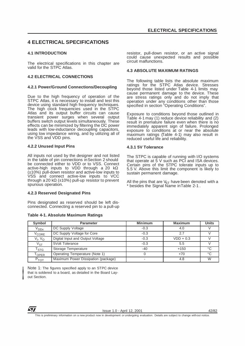
ELECTRICAL SPECIFICATIONS
Issue 1.0 - April 12, 2001 42/82This is preliminary information on a new product now in development or undergoing evaluation. Details are subject to change without notice.
4 ELECTRICAL SPECIFICATIONS
4.1 INTRODUCTION
The electrical specifications in this chapter arevalid for the STPC Atlas.
4.2 ELECTRICAL CONNECTIONS
4.2.1 Power/Ground Connections/Decoupling
Due to the high frequency of operation of theSTPC Atlas, it is necessary to install and test thisdevice using standard high frequency techniques.The high clock frequencies used in the STPCAtlas and its output buffer circuits can causetransient power surges when several outputbuffers switch output levels simultaneously. Theseeffects can be minimized by filtering the DC powerleads with low-inductance decoupling capacitors,using low impedance wiring, and by utilizing all ofthe VSS and VDD pins.
4.2.2 Unused Input Pins
All inputs not used by the designer and not listedin the table of pin connections inSection 2 shouldbe connected either to VDD or to VSS. Connectactive-high inputs to VDD through a 20 kΩ(±10%) pull-down resistor and active-low inputs toVSS and connect active-low inputs to VCCthrough a 20 kΩ (±10%) pull-up resistor to preventspurious operation.
4.2.3 Reserved Designated Pins
Pins designated as reserved should be left dis-connected. Connecting a reserved pin to a pull-up
resistor, pull-down resistor, or an active signalcould cause unexpected results and possiblecircuit malfunctions.
4.3 ABSOLUTE MAXIMUM RATINGS
The following table lists the absolute maximumratings for the STPC Atlas device. Stressesbeyond those listed under Table 4-1 limits maycause permanent damage to the device. Theseare stress ratings only and do not imply thatoperation under any conditions other than thosespecified in section ”Operating Conditions”.
Exposure to conditions beyond those outlined inTable 4-1 may (1) reduce device reliability and (2)result in premature failure even when there is noimmediately apparent sign of failure. Prolongedexposure to conditions at or near the absolutemaximum ratings (Table 4-1) may also result inreduced useful life and reliability.
4.3.1 5V Tolerance
The STPC is capable of running with I/O systemsthat operate at 5 V such as PCI and ISA devices.Certain pins of the STPC tolerate inputs up to5.5 V. Above this limit the component is likely tosustain permanent damage.
All the pins that are V5T have been denoted with a* besides the Signal Name inTable 2-1 .
Note 1: The figures specified apply to an STPC devicethat is soldered to a board, as detailed in the Board Lay-out Section.
Table 4-1. Absolute Maximum Ratings
Symbol Parameter Minimum Maximum UnitsVDDx DC Supply Voltage -0.3 4.0 V
VCORE DC Supply Voltage for Core -0.3 2.7 V
VI, VO Digital Input and Output Voltage -0.3 VDD + 0.3 VV5T 5Volt Tolerance -0.3 5.5 V
TSTG Storage Temperature -40 +150 °C
TOPER Operating Temperature (Note 1) 0 +70 °CPTOT Maximum Power Dissipation (package) - 4.8 W
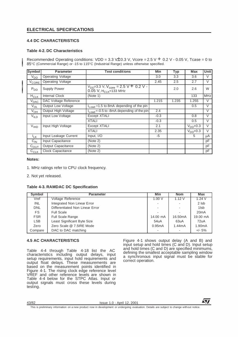
ELECTRICAL SPECIFICATIONS
43/82 Issue 1.0 - April 12, 2001This is preliminary information on a new product now in development or undergoing evaluation. Details are subject to change without notice.
4.4 DC CHARACTERISTICS
Notes:
1. MHz ratings refer to CPU clock frequency.
2. Not yet released.
4.5 AC CHARACTERISTICS
Table 4-4 through Table 4-18 list the ACcharacteristics including output delays, inputsetup requirements, input hold requirements andoutput float delays. These measurements arebased on the measurement points identified inFigure 4-1. The rising clock edge reference levelVREF and other reference levels are shown inTable 4-4 below for the STPC Atlas. Input oroutput signals must cross these levels duringtesting.
Figure 4-1 shows output delay (A and B) andinput setup and hold times (C and D). Input setupand hold times (C and D) are specified minimums,defining the smallest acceptable sampling windowa synchronous input signal must be stable forcorrect operation.
Table 4-2. DC Characteristics
Recommended Operating conditions: VDD = 3.3 V±0.3 V, Vcore = 2.5 V + 0.2 V - 0.05 V, Tcase = 0 to85°C (Commercial Range) or -15 to 115°C (Industrial Range) unless otherwise specified.
Symbol Parameter Test condit ions Min Typ Max UnitVDD Operating Voltage 3.0 3.3 3.6 V
VCORE Operating Voltage 2.45 2.5 2.7 V
PDD Supply PowerVDD=3.3 V, Vcore = 2.5 V + 0.2 V -0.05 V, HCLK=133 MHz
2.0 2.6 W
HCLK Internal Clock (Note 1) 133 MHz
VDAC DAC Voltage Reference 1.215 1.235 1.255 V
VOL Output Low Voltage ILoad =1.5 to 8mA depending of the pin 0.5 VVOH Output High Voltage ILoad =-0.5 to -8mA depending of the pin 2.4 V
VILD Input Low Voltage Except XTALI -0.3 0.8 V
XTALI -0.3 0.5 V
VIHD Input High Voltage Except XTALI 2.1 VDD+0.3 V
XTALI 2.35 VDD+0.3 VILK Input Leakage Current Input, I/O -5 5 µA
CIN Input Capacitance (Note 2) pF
COUT Output Capacitance (Note 2) pFCCLK Clock Capacitance (Note 2) pF
Table 4-3. RAMDAC DC Specification
Symbol Parameter Min Nom MaxVref Voltage Reference 1.00 V 1.12 V 1.24 VINL Integrated Non Linear Error - - 2 lsbDNL Differentiated Non Linear Error - - 1lsbFS Full Scale - - 20mA
FSR Full Scale Range 14.00 mA 16.50mA 19.00 mALSB Least Significant Byte Size 54uA 63uA 72uAZero Zero Scale @ 7.5IRE Mode 0.95mA 1.44mA 1.90mA
Compare DAC to DAC matching - - +/- 5%

ELECTRICAL SPECIFICATIONS
Issue 1.0 - April 12, 2001 44/82This is preliminary information on a new product now in development or undergoing evaluation. Details are subject to change without notice.
Note: Refer to Figure 4-1.
Table 4-4. Drive Level and Measurement Points for Switching Characteristics
Symbol Value UnitsVREF 1.5 V
VIHD 2.5 VVILD 0.0 V
Figure 4-1. Drive Level and Measurement Points for Switching Characteristics
CLK: VRef
VILD
VIHD
Tx
LEGEND: A - Maximum Output Delay SpecificationB - Minimum Output Delay SpecificationC - Minimum Input Setup SpecificationD - Minimum Input Hold Specification
VRef
Valid
ValidValidOUTPUTS:
INPUTS:
Output n Output n+1
Input
MAX
MIN
A
B
C D
VRef
VILD
VIHD

ELECTRICAL SPECIFICATIONS
45/82 Issue 1.0 - April 12, 2001This is preliminary information on a new product now in development or undergoing evaluation. Details are subject to change without notice.
4.5.1 POWER ON SEQUENCE
Strap O p tions
3 .3 V Supply
SYSR STI#
SYSR STO #
1 4 MH z
1.6 V
VALID C O N FIG U R ATIO N
> 1 0 us
H C LK
PC I_C LK
2 .3 ms
FR AME#
ISAC LK

ELECTRICAL SPECIFICATIONS
Issue 1.0 - April 12, 2001 46/82This is preliminary information on a new product now in development or undergoing evaluation. Details are subject to change without notice.
Table 4-5. SDRAM Bus AC Timing
Name Parameter Min Max Unit
t1 MCLKI to RAS#[1:0] Output Valid - 6.2 ns
t2 MCLKI to CAS#[1:0] Output Valid - 6.2 ns
t3 MCLKI to CS#[3:0] Output Valid - 7.6 ns
t4 MCLKI to DQM#[7:0] Output Valid - 8.1 ns
t5 MCLKI to MA[11:0] Output Valid - 6.2 ns
t6 MCLKI to MWE# Output Valid - 6.2 ns
t7 MCLKI to MD[63:0] Output Valid - 8.2 ns
t8 MD[63:0] setup to MCKLI (no RDCLK) 8.2 - ns
t9 MD[63:0] setup to MCKLI (RDCLK at min delay) 4.9 - ns
t10 MD[63:0] setup to MCKLI (RDCLK at mid delay) 4.0 - ns
t11 MD[63:0] setup to MCKLI (RDCLK at max delay) 3.0 - ns
t12 MD[63:0] hold from MCKLI (no RDCLK) 3.1 - ns
t13 MD[63:0] 0hold from MCKLI (RDCLK at min delay) 6.5 - ns
t14 MD[63:0] hold from MCKLI (RDCLK at mid delay) 7.1 - ns
t15 MD[63:0] hold from MCKLI (RDCLK at max delay) 8.5 - ns
Note; The figures are extrapolated from silicon characterisation results and design timing analysis
Table 4-6. PCI Bus AC Timing
Name Parameter Min Max Unit
t16 PCICLKI to any output - 12.8 ns
t17 Setup to PCICKLI 7.0 - ns
t18 Hold from PCICLKI 1.0 - ns
t19 PCICLKI to PCIGNT# output valid - 12.0 ns
t20 PCIREQ# setup to PCICLKI 12.0 - ns
t21 PCIREQ# hold to PCICLKI 0.0 - ns
Table 4-7. Graphics Adapter (VGA) AC Timing
Name Parameter Min Max Unitt21 DCLK to VSYNC valid 27 nst22 DCLK to HSYNC valid 27 ns

ELECTRICAL SPECIFICATIONS
47/82 Issue 1.0 - April 12, 2001This is preliminary information on a new product now in development or undergoing evaluation. Details are subject to change without notice.
Table 4-8. Video Input/TV Output AC Timing
Name Parameter Min Max Unitt56 VIN[7:0] setup to VCLK 5 ns
t57 VIN[7:0] hold from VCLK 4 ns
t58 VCLK to ODD_EVEN valid 15 nst59 VCLK to VCS valid 15 ns
t60 ODD_EVEN setup to VCLK 10 ns
t61 ODD_EVEN hold from VCLK 5 nst62 VCS setup to VCLK 10 ns
t63 VCS hold from VCLK 5 ns
Table 4-9. IPC Interface AC Timings
Name Parameter Min Max Unitt23 XTALO to DACK_EN[2:0] valid 71 nSt24 XTALO to TC valid 68 nSt25 IRQ_MUX Input setup to ISACLK2X 0 - nSt26 DREQ_MUX[1:0] Input setup to ISACLK2X 0 - nS

ELECTRICAL SPECIFICATIONS
Issue 1.0 - April 12, 2001 48/82This is preliminary information on a new product now in development or undergoing evaluation. Details are subject to change without notice.
4.5.2 ISA INTERFACE AC TIMING CHARACTERISTICS
Figure 4-2 ISA Cycle (ref Table 4-10)
Note 1: Stands for SMEMR#, SMEMW#, MEMR#, MEMW#, IOR# & IOW#.
The clock has not been represented as it is dependent on the ISA Slave mode.
Table 4-10. ISA Bus AC Timing
Name Parameter Min Max Units2 LA[23:17] valid before ALE# negated 5T Cycles
3 LA[23:17] valid before MEMR#, MEMW# asserted3a Memory access to 16-bit ISA Slave 5T Cycles
3b Memory access to 8-bit ISA Slave 5T Cycles9 SA[19:0] & SBHE valid before ALE# negated 1T Cycles
10 SA[19:0] & SBHE valid before MEMR#, MEMW# asserted10a Memory access to 16-bit ISA Slave 2T Cycles10b Memory access to 8-bit ISA Slave 2T Cycles
10 SA[19:0] & SHBE valid before SMEMR#, SMEMW# asserted10c Memory access to 16-bit ISA Slave 2T Cycle10d Memory access to 8-bit ISA Slave 2T Cycle
10e SA[19:0] & SBHE valid before IOR#, IOW# asserted 2T Cycles
11 XTALO to IOW# validNote: The signal numbering refers to Table 4-2
Valid AENx
Valid Address
Valid Address, SBHE*
V.Data
VALIDDATA
54
28
26
64
5958
55
28
23
61
4847
2623
5727
24
42
4110
11
3433
3
22
5629
259
18
2
12
3837
15
1413
12
ALE
AEN
LA [23:17 ]
SA [19:0]
CONTROL (Note 1)
IOCS16#
MCS16#
IOCHRDY
READ DATA
WRITE DATA

ELECTRICAL SPECIFICATIONS
49/82 Issue 1.0 - April 12, 2001This is preliminary information on a new product now in development or undergoing evaluation. Details are subject to change without notice.
11a Memory access to 16-bit ISA Slave - 2BCLK 2T Cycles
11b Memory access to 16-bit ISA Slave - Standard 3BCLK 2T Cycles11c Memory access to 16-bit ISA Slave - 4BCLK 2T Cycles
11d Memory access to 8-bit ISA Slave - 2BCLK 2T Cycles
11e Memory access to 8-bit ISA Slave - Standard 3BCLK 2T Cycles
12 ALE# asserted before ALE# negated 1T Cycles13 ALE# asserted before MEMR#, MEMW# asserted
13a Memory Access to 16-bit ISA Slave 2T Cycles
13b Memory Access to 8-bit ISA Slave 2T Cycles13 ALE# asserted before SMEMR#, SMEMW# asserted
13c Memory Access to 16-bit ISA Slave 2T Cycles
13d Memory Access to 8-bit ISA Slave 2T Cycles
13e ALE# asserted before IOR#, IOW# asserted 2T Cycles14 ALE# asserted before AL[23:17]
14a Non compressed 15T Cycles
14b Compressed 15T Cycles
15 ALE# asserted before MEMR#, MEMW#, SMEMR#, SMEMW# negated15a Memory Access to 16-bit ISA Slave- 4 BCLK 11T Cycles15e Memory Access to 8-bit ISA Slave- Standard Cycle 11T Cycles
18a ALE# negated before LA[23:17] invalid (non compressed) 14T Cycles
18a ALE# negated before LA[23:17] invalid (compressed) 14T Cycles22 MEMR#, MEMW# asserted before LA[23:17]
22a Memory access to 16-bit ISA Slave. 13T Cycles
22b Memory access to 8-bit ISA Slave. 13T Cycles23 MEMR#, MEMW# asserted before MEMR#, MEMW# negated
23b Memory access to 16-bit ISA Slave Standard cycle 9T Cycles
23e Memory access to 8-bit ISA Slave Standard cycle 9T Cycles23 SMEMR#, SMEMW# asserted before SMEMR#, SMEMW# negated
23h Memory access to 16-bit ISA Slave Standard cycle 9T Cycles23l Memory access to 16-bit ISA Slave Standard cycle 9T Cycles
23 IOR#, IOW# asserted before IOR#, IOW# negated23o Memory access to 16-bit ISA Slave Standard cycle 9T Cycles23r Memory access to 8-bit ISA Slave Standard cycle 9T Cycles
24 MEMR#, MEMW# asserted before SA[19:0]24b Memory access to 16-bit ISA Slave Standard cycle 10T Cycles24d Memory access to 8-bit ISA Slave - 3BLCK 10T Cycles
24e Memory access to 8-bit ISA Slave Standard cycle 10T Cycles
24f Memory access to 8-bit ISA Slave - 7BCLK 10T Cycles24 SMEMR#, SMEMW# asserted before SA[19:0]
24h Memory access to 16-bit ISA Slave Standard cycle 10T Cycles
24i Memory access to 16-bit ISA Slave - 4BCLK 10T Cycles
24k Memory access to 8-bit ISA Slave - 3BCLK 10T Cycles
24l Memory access to 8-bit ISA Slave Standard cycle 10T Cycles24 IOR#, IOW# asserted before SA[19:0]
24o I/O access to 16-bit ISA Slave Standard cycle 19T Cycles
24r I/O access to 16-bit ISA Slave Standard cycle 19T Cycles
Table 4-10. ISA Bus AC Timing
Name Parameter Min Max Units
Note: The signal numbering refers to Table 4-2
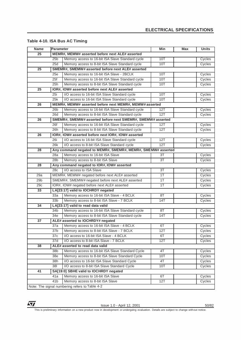
ELECTRICAL SPECIFICATIONS
Issue 1.0 - April 12, 2001 50/82This is preliminary information on a new product now in development or undergoing evaluation. Details are subject to change without notice.
25 MEMR#, MEMW# asserted before next ALE# asserted25b Memory access to 16-bit ISA Slave Standard cycle 10T Cycles
25d Memory access to 8-bit ISA Slave Standard cycle 10T Cycles
25 SMEMR#, SMEMW# asserted before next ALE# asserted25e Memory access to 16-bit ISA Slave - 2BCLK 10T Cycles
25f Memory access to 16-bit ISA Slave Standard cycle 10T Cycles25h Memory access to 8-bit ISA Slave Standard cycle 10T Cycles
25 IOR#, IOW# asserted before next ALE# asserted25i I/O access to 16-bit ISA Slave Standard cycle 10T Cycles25k I/O access to 16-bit ISA Slave Standard cycle 10T Cycles
26 MEMR#, MEMW# asserted before next MEMR#, MEMW# asserted26b Memory access to 16-bit ISA Slave Standard cycle 12T Cycles26d Memory access to 8-bit ISA Slave Standard cycle 12T Cycles
26 SMEMR#, SMEMW# asserted before next SMEMR#, SMEMW# asserted26f Memory access to 16-bit ISA Slave Standard cycle 12T Cycles26h Memory access to 8-bit ISA Slave Standard cycle 12T Cycles
26 IOR#, IOW# asserted before next IOR#, IOW# asserted26i I/O access to 16-bit ISA Slave Standard cycle 12T Cycles
26k I/O access to 8-bit ISA Slave Standard cycle 12T Cycles
28 Any command negated to MEMR#, SMEMR#, MEMR#, SMEMW# asserted28a Memory access to 16-bit ISA Slave 3T Cycles
28b Memory access to 8-bit ISA Slave 3T Cycles
28 Any command negated to IOR#, IOW# asserted28c I/O access to ISA Slave 3T Cycles
29a MEMR#, MEMW# negated before next ALE# asserted 1T Cycles
29b SMEMR#, SMEMW# negated before next ALE# asserted 1T Cycles29c IOR#, IOW# negated before next ALE# asserted 1T Cycles
33 LA[23:17] valid to IOCHRDY negated33a Memory access to 16-bit ISA Slave - 4 BCLK 8T Cycles
33b Memory access to 8-bit ISA Slave - 7 BCLK 14T Cycles
34 LA[23:17] valid to read data valid34b Memory access to 16-bit ISA Slave Standard cycle 8T Cycles
34e Memory access to 8-bit ISA Slave Standard cycle 14T Cycles
37 ALE# asserted to IOCHRDY# negated37a Memory access to 16-bit ISA Slave - 4 BCLK 6T Cycles
37b Memory access to 8-bit ISA Slave - 7 BCLK 12T Cycles
37c I/O access to 16-bit ISA Slave - 4 BCLK 6T Cycles37d I/O access to 8-bit ISA Slave - 7 BCLK 12T Cycles
38 ALE# asserted to read data valid38b Memory access to 16-bit ISA Slave Standard Cycle 4T Cycles
38e Memory access to 8-bit ISA Slave Standard Cycle 10T Cycles
38h I/O access to 16-bit ISA Slave Standard Cycle 4T Cycles38l I/O access to 8-bit ISA Slave Standard Cycle 10T Cycles
41 SA[19:0] SBHE valid to IOCHRDY negated41a Memory access to 16-bit ISA Slave 6T Cycles41b Memory access to 8-bit ISA Slave 12T Cycles
Table 4-10. ISA Bus AC Timing
Name Parameter Min Max Units
Note: The signal numbering refers to Table 4-2
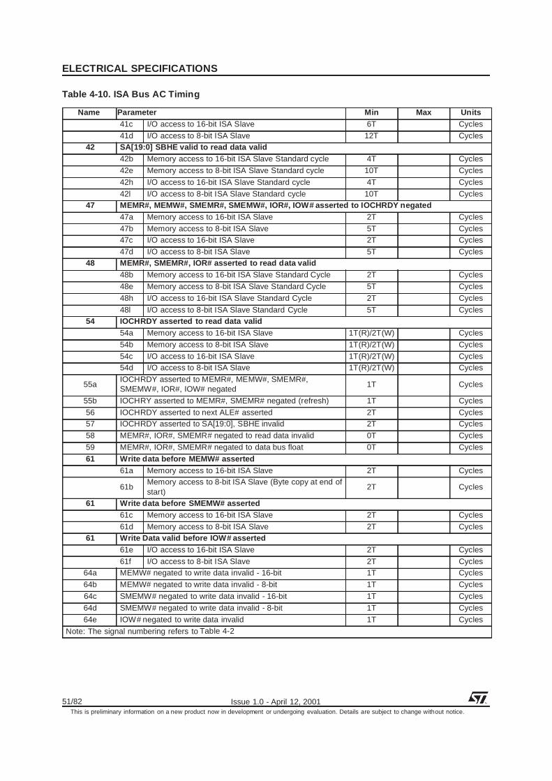
ELECTRICAL SPECIFICATIONS
51/82 Issue 1.0 - April 12, 2001This is preliminary information on a new product now in development or undergoing evaluation. Details are subject to change without notice.
41c I/O access to 16-bit ISA Slave 6T Cycles
41d I/O access to 8-bit ISA Slave 12T Cycles42 SA[19:0] SBHE valid to read data valid
42b Memory access to 16-bit ISA Slave Standard cycle 4T Cycles
42e Memory access to 8-bit ISA Slave Standard cycle 10T Cycles
42h I/O access to 16-bit ISA Slave Standard cycle 4T Cycles
42l I/O access to 8-bit ISA Slave Standard cycle 10T Cycles47 MEMR#, MEMW#, SMEMR#, SMEMW#, IOR#, IOW# asserted to IOCHRDY negated
47a Memory access to 16-bit ISA Slave 2T Cycles
47b Memory access to 8-bit ISA Slave 5T Cycles47c I/O access to 16-bit ISA Slave 2T Cycles
47d I/O access to 8-bit ISA Slave 5T Cycles48 MEMR#, SMEMR#, IOR# asserted to read data valid
48b Memory access to 16-bit ISA Slave Standard Cycle 2T Cycles
48e Memory access to 8-bit ISA Slave Standard Cycle 5T Cycles
48h I/O access to 16-bit ISA Slave Standard Cycle 2T Cycles
48l I/O access to 8-bit ISA Slave Standard Cycle 5T Cycles54 IOCHRDY asserted to read data valid
54a Memory access to 16-bit ISA Slave 1T(R)/2T(W) Cycles
54b Memory access to 8-bit ISA Slave 1T(R)/2T(W) Cycles
54c I/O access to 16-bit ISA Slave 1T(R)/2T(W) Cycles54d I/O access to 8-bit ISA Slave 1T(R)/2T(W) Cycles
55aIOCHRDY asserted to MEMR#, MEMW#, SMEMR#,SMEMW#, IOR#, IOW# negated
1T Cycles
55b IOCHRY asserted to MEMR#, SMEMR# negated (refresh) 1T Cycles
56 IOCHRDY asserted to next ALE# asserted 2T Cycles57 IOCHRDY asserted to SA[19:0], SBHE invalid 2T Cycles
58 MEMR#, IOR#, SMEMR# negated to read data invalid 0T Cycles
59 MEMR#, IOR#, SMEMR# negated to data bus float 0T Cycles
61 Write data before MEMW# asserted61a Memory access to 16-bit ISA Slave 2T Cycles
61bMemory access to 8-bit ISA Slave (Byte copy at end ofstart)
2T Cycles
61 Write data before SMEMW# asserted61c Memory access to 16-bit ISA Slave 2T Cycles
61d Memory access to 8-bit ISA Slave 2T Cycles61 Write Data valid before IOW# asserted
61e I/O access to 16-bit ISA Slave 2T Cycles
61f I/O access to 8-bit ISA Slave 2T Cycles64a MEMW# negated to write data invalid - 16-bit 1T Cycles
64b MEMW# negated to write data invalid - 8-bit 1T Cycles
64c SMEMW# negated to write data invalid - 16-bit 1T Cycles
64d SMEMW# negated to write data invalid - 8-bit 1T Cycles
64e IOW# negated to write data invalid 1T Cycles
Table 4-10. ISA Bus AC Timing
Name Parameter Min Max Units
Note: The signal numbering refers to Table 4-2
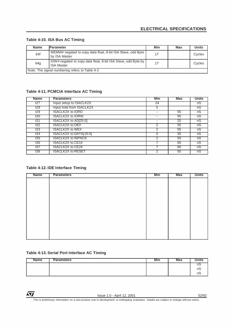
ELECTRICAL SPECIFICATIONS
Issue 1.0 - April 12, 2001 52/82This is preliminary information on a new product now in development or undergoing evaluation. Details are subject to change without notice.
64fMEMW# negated to copy data float, 8-bit ISA Slave, odd Byteby ISA Master
1T Cycles
64gIOW# negated to copy data float, 8-bit ISA Slave, odd Byte byISA Master
1T Cycles
Table 4-10. ISA Bus AC Timing
Name Parameter Min Max Units
Note: The signal numbering refers to Table 4-2
Table 4-11. PCMCIA Interface AC Timing
Name Parameters Min Max Unitst27 Input setup to ISACLK2X 24 nSt28 Input hold from ISACLK2X 5 nSt29 ISACLK2X to IORD - 55 nSt30 ISACLK2X to IORW - 55 nSt31 ISACLK2X to AD[25:0] - 25 nSt32 ISACLK2X to OE# 2 55 nSt33 ISACLK2X to WE# 2 55 nSt34 ISACLK2X to DATA[15:0] 0 35 nSt35 ISACLK2X to INPACK 2 55 nSt36 ISACLK2X to CE1# 7 65 nSt37 ISACLK2X to CE2# 7 65 nSt38 ISACLK2X to RESET 2 55 nS
Table 4-12. IDE Interface Timing
Name Parameters Min Max Units
Table 4-13. Serial Port Interface AC Timing
Name Parameters Min Max UnitsnSnSnS
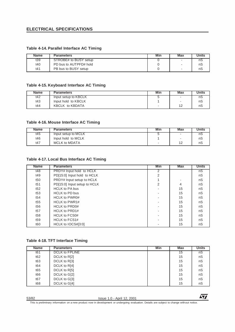
ELECTRICAL SPECIFICATIONS
53/82 Issue 1.0 - April 12, 2001This is preliminary information on a new product now in development or undergoing evaluation. Details are subject to change without notice.
Table 4-14. Parallel Interface AC Timing
Name Parameters Min Max Unitst39 STROBE# to BUSY setup 0 - nSt40 PD bus to AUTPFD# hold 0 - nSt41 PB bus to BUSY setup 0 - nS
Table 4-15. Keyboard Interface AC Timing
Name Parameters Min Max Unitst42 Input setup to KBCLK 5 - nSt43 Input hold to KBCLK 1 - nSt44 KBCLK to KBDATA - 12 nS
Table 4-16. Mouse Interface AC Timing
Name Parameters Min Max Unitst45 Input setup to MCLK 5 - nSt46 Input hold to MCLK 1 - nSt47 MCLK to MDATA - 12 nS
Table 4-17. Local Bus Interface AC Timing
Name Parameters Min Max Unitst48 PRDY# Input hold to HCLK 2 nSt49 PD[15:0] Input hold to HCLK 2 nSt50 PRDY# Input setup to HCLK 1 - nSt51 PD[15:0] Input setup to HCLK 2 4 nSt52 HCLK to PA bus - 15 nSt53 HCLK to PD bus - 15 nSt54 HCLK to PWR0# - 15 nSt55 HCLK to PWR1# - 15 nSt56 HCLK to PRD0# - 15 nSt57 HCLK to PRD1# - 15 nSt58 HCLK to FCS0# - 15 nSt59 HCLK to FCS1# - 15 nSt60 HCLK to IOCS#[3:0] - 15 nS
Table 4-18. TFT Interface Timing
Name Parameters Min Max Unitst61 DCLK to FPLINE 15 nSt62 DCLK to R[2] 15 nSt63 DCLK to R[3] 15 nSt64 DCLK to R[4] 15 nSt65 DCLK to R[5] 15 nSt66 DCLK to G[2] 15 nSt67 DCLK to G[3] 15 nSt68 DCLK to G[4] 15 nS

ELECTRICAL SPECIFICATIONS
Issue 1.0 - April 12, 2001 54/82This is preliminary information on a new product now in development or undergoing evaluation. Details are subject to change without notice.
t69 DCLK to G[5] 15 nSt70 DCLK to B[2] 15 nSt71 DCLK to B[3] 15 nSt72 DCLK to B[4] 15 nSt73 DCLK to B[5] 15 nSt74 DCLK to FPFRAME 15 nS
Table 4-18. TFT Interface Timing
Name Parameters Min Max Units
Table 4-19. USB Interface Timing
Name Parameters Min Max Units

ELECTRICAL SPECIFICATIONS
55/82 Issue 1.0 - April 12, 2001This is preliminary information on a new product now in development or undergoing evaluation. Details are subject to change without notice.
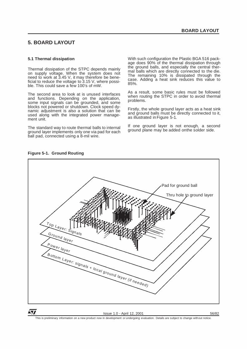
BOARD LAYOUT
Issue 1.0 - April 12, 2001 56/82This is preliminary information on a new product now in development or undergoing evaluation. Details are subject to change without notice.
5. BOARD LAYOUT
5.1 Thermal dissipation
Thermal dissipation of the STPC depends mainlyon supply voltage. When the system does notneed to work at 3.45 V, it may therefore be bene-ficial to reduce the voltage to 3.15 V, where possi-ble. This could save a few 100’s of mW.
The second area to look at is unused interfacesand functions. Depending on the application,some input signals can be grounded, and someblocks not powered or shutdown. Clock speed dy-namic adjustment is also a solution that can beused along with the integrated power manage-ment unit.
The standard way to route thermal balls to internalground layer implements only one via pad for eachball pad, connected using a 8-mil wire.
With such configuration the Plastic BGA 516 pack-age does 90% of the thermal dissipation throughthe ground balls, and especially the central ther-mal balls which are directly connected to the die.The remaining 10% is dissipated through thecase. Adding a heat sink reduces this value to85%.
As a result, some basic rules must be followedwhen routing the STPC in order to avoid thermalproblems.
Firstly, the whole ground layer acts as a heat sinkand ground balls must be directly connected to it,as illustrated in Figure 5-1.
If one ground layer is not enough, a secondground plane may be added onthe solder side.
Figure 5-1. Ground Routing
Thru hole to ground layer
Top Layer: Signa lsG round layerP ow er layerB ottom Layer: signa ls + loca l ground layer (if needed)
Pad for ground ball

BOARD LAYOUT
57/82 Issue 1.0 - April 12, 2001This is preliminary information on a new product now in development or undergoing evaluation. Details are subject to change without notice.
When considering thermal dissipation, the mostimportant - and notalways the most obvious - partof the layout is the connection between the groundballs and the ground layer.
A 1-wire connection is shown in Figure 5-2. Theuse of a 8-mil wire results in a thermal resistanceof 105°C/W assuming copper is used (418 W/m.°K). This high value is due to the thickness (34µm) of the copper on the external side of the PCB.
Considering only the central matrix of 36 thermalballs and one via for each ball, the global thermalresistance is 2.9°C/W. This can be easily im-proved using four 10 mil wires to connect to thefour vias around the ground pad link as inFigure5-3. This gives a total of 49 vias and a global re-sistance for the 36 thermal balls of 0.6°C/W.
The use of a ground plane like in Figure 5-4 iseven better.
To avoid solder wicking over to the via pads duringsoldering, it is important to have a solder mask of4 mil around the pad (NSMD pad). This gives a di-ameter of 33 mil for a 25 mil ground pad.
To obtain the optimum ground layout, place thevias directly under the ball pads. In this case no lo-cal board distortion is tolerated.
The thickness of the copper on PCB layers is typ-ically 34 µm for external layers and 17 µm for in-ternal layers. This means that thermal dissipationis not good; high board temperatures are concen-trated around the devices and these fall quicklywith increased distance.
Where possible, place a metal layer inside thePCB; this improves dramatically the spread ofheat and hence the thermal dissipation of theboard.
Figure 5-2. Recommended 1-wire Ground Pad Layout
Figure 5-3. Recommended 4-wire Ground Pad Layout
Solder Mask (4 mil)
Pad for ground ball (diameter = 25 mil)
Hole to ground layer (diameter = 12 mil)
Connection Wire (width = 10 mil)
Via (diameter = 24 mil)34.5m
il
1 mil = 0.0254 mm
4 via pads for each ground ball

BOARD LAYOUT
Issue 1.0 - April 12, 2001 58/82This is preliminary information on a new product now in development or undergoing evaluation. Details are subject to change without notice.
The PBGA Package also dissipates heat throughperipheral ground balls. When a heat sink isplaced on the device, heat is more uniformlyspread throughout the moulding, increasing heatdissipation through the peripheral ground balls.
The more via pads that are connected to eachground ball, the more heat is dissipated. The onlylimitation is the risk of losing routing channels.
Figure 5-5 shows a routing with a good trade offbetween thermal dissipation and the number ofrouting channels.
Figure 5-4. OptimumLlayout for Central Ground Ball
Via to Ground layer
Pad for ground ball
Clearance = 6mil
diameter = 25 mil
hole diameter = 14 mil
Solder maskdiameter = 33 mil
External diameter = 37 mil
connections = 10 mil
Figure 5-5. Global Ground Layout for Good Thermal Dissipation
Top View
1
A
Via to ground layer
G round pad
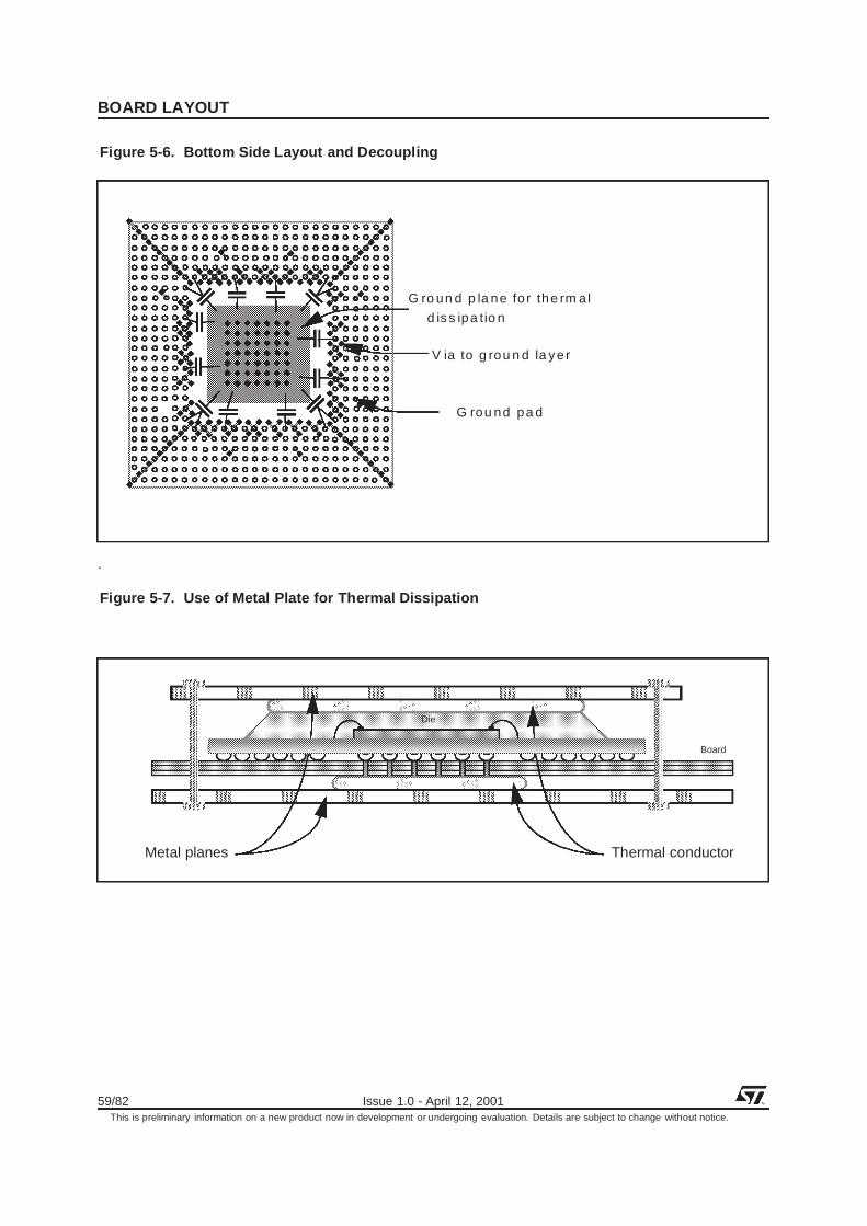
BOARD LAYOUT
59/82 Issue 1.0 - April 12, 2001This is preliminary information on a new product now in development or undergoing evaluation. Details are subject to change without notice.
.
Figure 5-6. Bottom Side Layout and Decoupling
d is s ipa tio n
G ro un d p la ne fo r the rm a l
V ia to g rou n d la y er
G rou nd pa d
Figure 5-7. Use of Metal Plate for Thermal Dissipation
Metal planes Thermal conductor
Board
Die

BOARD LAYOUT
Issue 1.0 - April 12, 2001 60/82This is preliminary information on a new product now in development or undergoing evaluation. Details are subject to change without notice.
Figure 5-8. Power Ball Routing
S T P C 3.3 V B a ll
S T P C 2.5 V B a ll
V ia
S T P C B a ll
To p V ie w
1A

BOARD LAYOUT
61/82 Issue 1.0 - April 12, 2001This is preliminary information on a new product now in development or undergoing evaluation. Details are subject to change without notice.
A local ground plane on opposite sides of theboard, as shown in Figure 5-6, improves thermaldissipation. It is used to connect decoupling ca-pacitances but it can also be used for connectionto a heat sink or to the system metal box for betterdissipation.The possibility of using the whole sys-tem box for thermal dissipation is very useful incases of high internal temperatures and low out-side temperatures. Both sides of the PBGA shouldbe thermally connected to the metal chassis in or-der to propagate the heat flow through the metal.Figure 5-7 illustrates such an implementation.
The routing to the 2.5 V and 3.3 V supply balls isshown in Figure 5-8.
5.2 High Speed Signals
Some STPC Interfaces run at high speed andneed to be carefully routed or even shielded.
Such interfaces are listed below, in decreasingspeed order:
1) Memory Interface
2) Graphics and video interfaces
3) PCI bus
4) 14 MHz oscillator stage
All clock signals have to be routed first and shield-ed for speeds of 27MHz or higher. The high speedsignals follow the same constraints, as for thememory and PCI control signals.
The next interfaces to be routed are Memory, Vid-eo/graphics and PCI.
All the analog noise-sensitive signals have to berouted in a separate area and hence can be rout-ed indepedently.
5.3 Memory Interface
5.3.1 Introduction
In order to achieve SDRAM memory interfaceswhich work at clock frequencies of 100 MHz andabove, careful consideration has to be given to thetiming of the interface with all the various electricaland physical constraints taken into consideration.The guidelines described below are related to
SDRAM components on DIMM modules. For ap-plications where the memories are directly sol-dered to the motherboard, the PCB should be laidout such that the trace lengths fit within the con-straints shown here. The traces could be slightlylonger since the extra routing on the DIMM PCB isno longer present but it is then up to the user toverify the timings.
5.3.2 SDRAM Clocking Scheme
The SDRAM Clocking Scheme deserves a specialmention here. Basically the memory clock is gen-erated on-chip through a PLL and goes directly tothe MCLKO output pin of the STPC. The nominalfrequency is 100 MHz. Because of the high loadpresented to the MCLK on the board by theDIMMs it is recommended to rebuffer the MCLKOsignal on the board and balance the skew to theclock ports of the different DIMMs and the MCLKIinput pin of STPC.

BOARD LAYOUT
Issue 1.0 - April 12, 2001 62/82This is preliminary information on a new product now in development or undergoing evaluation. Details are subject to change without notice.
Figure 5-9. Shielding signals
ground ring
ground pad
shielded signal line
ground padshielded signal lines

BOARD LAYOUT
63/82 Issue 1.0 - April 12, 2001This is preliminary information on a new product now in development or undergoing evaluation. Details are subject to change without notice.
Figure 5-10. Clock Scheme
DIM
M1
M CLK I
M CLKO
DIM
M2
PLL
register
PLL
M A[] + C ontrol
M D[]SD RAM
CO NTR O LLER
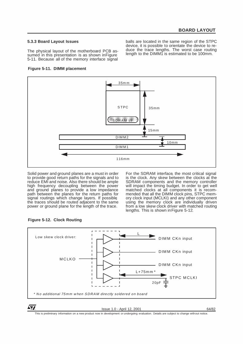
BOARD LAYOUT
Issue 1.0 - April 12, 2001 64/82This is preliminary information on a new product now in development or undergoing evaluation. Details are subject to change without notice.
5.3.3 Board Layout Issues
The physical layout of the motherboard PCB as-sumed in this presentation is as shown inFigure5-11. Because all of the memory interface signal
balls are located in the same region of the STPCdevice, it is possible to orientate the device to re-duce the trace lengths. The worst case routinglength to the DIMM1 is estimated to be 100mm.
Solid power and ground planes are a must in orderto provide good return paths for the signals and toreduce EMI and noise. Also there should be amplehigh frequency decoupling between the powerand ground planes to provide a low impedancepath between the planes for the return paths forsignal routings which change layers. If possible,the traces should be routed adjacent to the samepower or ground plane for the length of the trace.
For the SDRAM interface, the most critical signalis the clock. Any skew between the clocks at theSDRAM components and the memory controllerwill impact the timing budget. In order to get wellmatched clocks at all components it is recom-mended that all the DIMM clock pins, STPC mem-ory clock input (MCLKI) and any other componentusing the memory clock are individually drivenfrom a low skew clock driver with matched routinglengths. This is shown inFigure 5-12.
Figure 5-11. DIMM placement
DIM M 2
DIM M 1
S TPC
35m m
35mm
15mm
10mm
116mm
S DRA M I/F
Figure 5-12. Clock Routing
M C LKO
D IM M CKn input
STPC M C LKI
D IM M CKn input
D IM M CKn input
Low s kew clock d rive r:L
L+75m m *
20pF
* N o additional 75m m w hen S DRA M directly so ldered on board
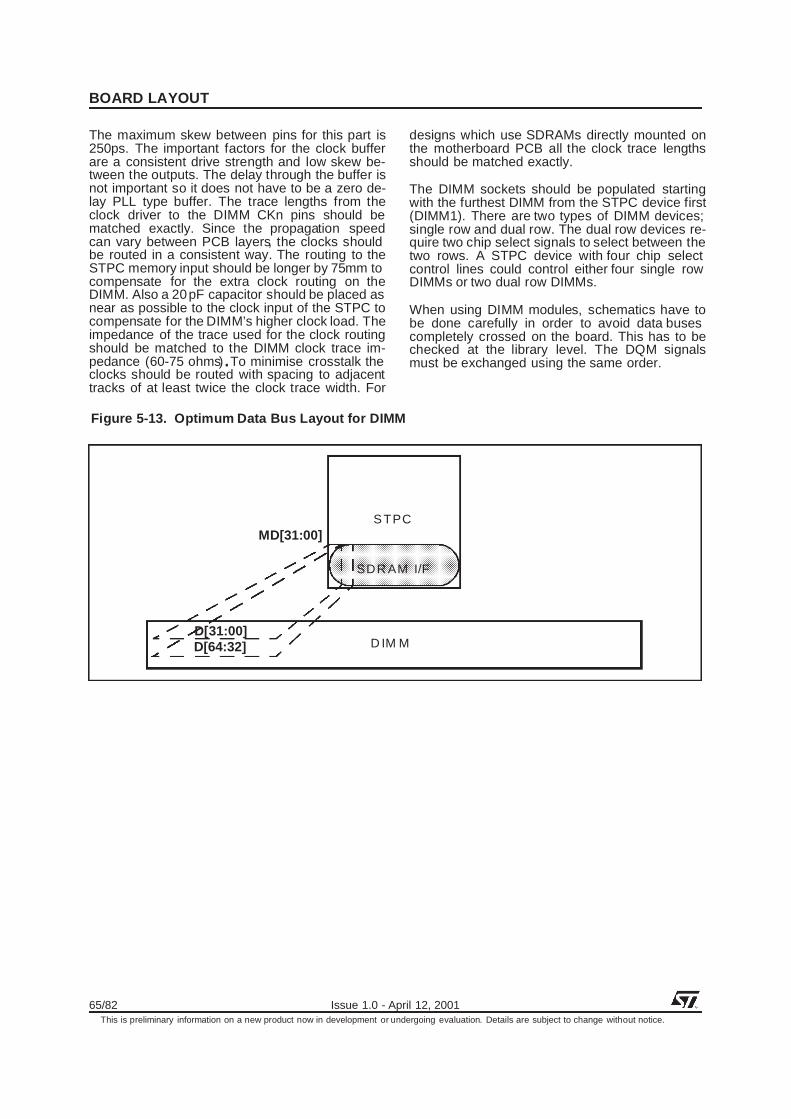
BOARD LAYOUT
65/82 Issue 1.0 - April 12, 2001This is preliminary information on a new product now in development or undergoing evaluation. Details are subject to change without notice.
The maximum skew between pins for this part is250ps. The important factors for the clock bufferare a consistent drive strength and low skew be-tween the outputs. The delay through the buffer isnot important so it does not have to be a zero de-lay PLL type buffer. The trace lengths from theclock driver to the DIMM CKn pins should bematched exactly. Since the propagation speedcan vary between PCB layers, the clocks shouldbe routed in a consistent way. The routing to theSTPC memory input should be longer by 75mm tocompensate for the extra clock routing on theDIMM. Also a 20pF capacitor should be placed asnear as possible to the clock input of the STPC tocompensate for the DIMM’s higher clock load. Theimpedance of the trace used for the clock routingshould be matched to the DIMM clock trace im-pedance (60-75 ohms).To minimise crosstalk theclocks should be routed with spacing to adjacenttracks of at least twice the clock trace width. For
designs which use SDRAMs directly mounted onthe motherboard PCB all the clock trace lengthsshould be matched exactly.
The DIMM sockets should be populated startingwith the furthest DIMM from the STPC device first(DIMM1). There are two types of DIMM devices;single row and dual row. The dual row devices re-quire two chip select signals to select between thetwo rows. A STPC device with four chip selectcontrol lines could control either four single rowDIMMs or two dual row DIMMs.
When using DIMM modules, schematics have tobe done carefully in order to avoid data busescompletely crossed on the board. This has to bechecked at the library level. The DQM signalsmust be exchanged using the same order.
Figure 5-13. Optimum Data Bus Layout for DIMM
D IM M
STPC
SDR AM I/F
D[31:00]D[64:32]
MD[31:00]

BOARD LAYOUT
Issue 1.0 - April 12, 2001 66/82This is preliminary information on a new product now in development or undergoing evaluation. Details are subject to change without notice.
5.3.4 Address & Control Signals
This group encompasses the memory addressMA[10:0], bank address BA[0], RAS, CAS andwrite enable WE signals. The load of the DIMMmodule on these signals is the most important oneand depends upon the type of SDRAM compo-
nents used (x4, x8 or x16) and whether the DIMMmodule is single or dual row. The capacitive load-ing of the SDRAM inputs alone for an x8 singlerow DIMM will be about 30-40 pF. An equivalentcircuit for the timing simulation is shown inFigure5-14 Most of the delays are due to the PCB tracesand loading rather than the pad itself.
Figure 5-14. Address/Control Equivalent Circuit
DIM
M2
DIM
M1
Rterm100mm(0.7ns)
10mmZØpcb
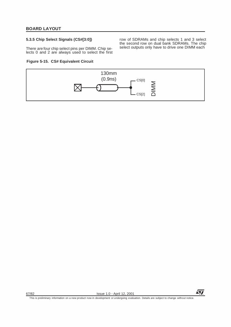
BOARD LAYOUT
67/82 Issue 1.0 - April 12, 2001This is preliminary information on a new product now in development or undergoing evaluation. Details are subject to change without notice.
5.3.5 Chip Select Signals (CS#[3:0])
There are four chip select pins per DIMM. Chip se-lects 0 and 2 are always used to select the first
row of SDRAMs and chip selects 1 and 3 selectthe second row on dual bank SDRAMs. The chipselect outputs only have to drive one DIMM each
Figure 5-15. CS# Equivalent Circuit
130mm(0.9ns)
DIM
M
CS[0]
CS[2]
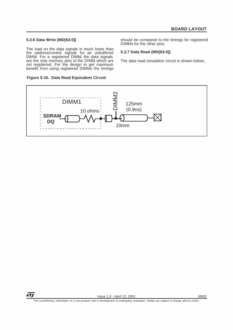
BOARD LAYOUT
Issue 1.0 - April 12, 2001 68/82This is preliminary information on a new product now in development or undergoing evaluation. Details are subject to change without notice.
5.3.6 Data Write (MD[63:0])
The load on the data signals is much lower thanthe address/control signals for an unbufferedDIMM. For a registered DIMM, the data signalsare the only memory pins of the DIMM which arenot registered. For the design to get maximumbenefit from using registered DIMMs the timings
should be compared to the timings for registeredDIMMs for the other pins.
5.3.7 Data Read (MD[63:0])
The data read simulation circuit is shown below..
Figure 5-16. Data Read Equivalent Circuit
125mm(0.9ns)D
IMM
2
10mm
10 ohmsSDRAM
DQ
DIMM1
BOARD LAYOUT
69/82 Issue 1.0 - April 12, 2001This is preliminary information on a new product now in development or undergoing evaluation. Details are subject to change without notice.
5.3.8 Data Mask (DQM[7:0])
The data mask load is quite similar to that of thedata signals.
5.3.9 Summary
For unbuffered DIMMs the address/control signalswill be the most critical for timing. The simulationsshow that for these signals the best way to drivethem is to use a parallel termination. For applica-tions where speed is not so critical series termina-tion can be used as this will save power. Using alow impedance such as 50Ω for these critical trac-es is recommended as it both reduces the delayand the overshoot.
The other memory interface signals will typicallybe not as critical as the address/control signals forunbuffered DIMMs. When using registered DIMMsthe other signals will probably be just as critical asthe address/control signals so to gain maximumbenefit from using registered DIMMs the timingsshould also be considered in that situation. Usinglower impedance traces is also beneficial for theother signals but if their timing is not as critical asthe address/control signals they could use the de-fault value. Using a lower impedance implies us-ing wider traces which may have an impact on therouting of the board.
5.4 SDRAM LAYOUT EXAMPLES
The STPC provides MA, RAS#, CAS#, WE#, CS#,DQM#, BA0 (MA[11])and MD for SDRAM control.From 2 to 128 MBytes of main memory are sup-ported in 1 to 4 banks. All Banks must be 64 bitswide.
The following memory devices are supported:
4Mbit x 4, 8Mbit x 2 & 16Mbit x 1 or if in the case oftwo internal bank chips, 2Mbit x 4 x 2, 4Mbit x 2 x2 & 8Mbit x 1 x 2.
The following Figure 5-17 and Figure 5-18, showstwo possible SDRAM organizations based on oneor two bank configurations.
Notes for Figure 5-17 and Figure 5-18;
All buffers must be low skew clock buffers
One clock driver can operate up to four memorychips.
All the clock lines must follow the rules below;
MCLKI = MCLK0 + MCLK0A
=......
= MCLK0 + MCLK0D
= MCLK1 + MCLK1A
=......
= MCLK1 + MCLK1D
This means that all line lengths must go from thebuffer to the memory chips (MCLK1 or MCLK0or...) and from the buffer to the STPC (MCLKI)must be identical.
5.4.1 Host Address to MA Bus Mapping
Graphics memory resides at the beginning ofBank 0. Host memory begins at the top of graphicsmemory and extends to the top of populatedSDRAM.
The bank attributes can be retrieved from a lookuptable to select the final SDRAM row and columnaddress mappings. (Table 5-2). Table 5-1 showsthe Standard DIMM Pinout for users wishing to de-sign with DIMMs.
.

BO
AR
DLA
YO
UT
Issue1.0
-A
pril12,200170/82
This
isp
reliminary
information
ona
new
productnow
indevelopm
ento
rundergoin
gevaluation.
Details
are
subjectto
changew
ithout
notice.
Figure
5-17.O
neM
emory
Bank
with
EightC
hips(8-B
it)
On
eM
emory
Bank
with
Eight
Devices
(8-bit)
CS0#BA0 (M A[11])M A[10:0]
WE#
(Each signal needs
RAS0#
DQM#
MD[63:0]
MCLKI
M CLKO
MCLK0B MCLK0C
16 MBit
8-bit wide
16 MBit
8-bit wide
it’s own line)
16 MBit
8-bit wide
16 MBit
8-bit wide
DQM[3:2]
DQM[5:4]
DQM[1:0]
Reference Knot
MCLK0A MCLK0D
[63:48]MD
[47:32]MD
[31:16]MD
[15:0]MDDQM
[7:6]
CAS#0

BOARD LAYOUT
71/82 Issue 1.0 - April 12, 2001This is preliminary information on a new product now in development or undergoing evaluation. Details are subject to change without notice.
Figure 5-18. Two Memory Banks with Eight Chips on Each (8-Bit)
Two Memory bank with eight devices (8-bit)
CA
S#
1,
RA
S#
1C
S1
#,3
#,
WE
#
MA
[10
:0]
(Ea
ch
sig
na
ln
ee
ds
it’s
ow
nlin
e)
CA
S#
0,
RA
S#
0C
S0
#,2
#,
WE
#
MA
[10
:0]
(Ea
chsi
gn
al
ne
ed
sit’
so
wn
line
)
BA
0(M
A[1
1])
MC
LK
I
MC
KL
OM
CL
K0
/1
MC
LK
2/3
DQ
M [7]
DQ
M#
MD
[63
:0]
16
MB
it
8-b
itw
ide
MC
LK0
BM
CL
K1A
16
MB
it
8-b
itw
ide
16
MB
it
8-b
itw
ide
16
MB
it
8-b
itw
ide
MC
LK
2A
16
MB
it
8-b
itw
ide
16
MB
it
8-b
itw
ide
16
MB
it
8-b
itw
ide
16
MB
it
8-b
itw
ide
DQ
M [1]
DQ
M [2]
DQ
M [3]
DQ
M [4]
DQ
M [5]
DQ
M [0]
[63
:56
]
MC
LK
0A
MC
LK
1B
MC
LK
2BM
CL
K3B
MC
LK3
A
MD
[55
:48
]M
D[4
7:4
0]
MD
[39
:32
]M
D[3
1:2
4]
MD
[15
:8]
MD
[7:0
]
MD
DQ
M [6]
Clo
ck
Bu
ffe
rC
om
pu
lso
ry
[23
:16
]M
D
MC
LK
4/5
MC
LK
6/7
BA
0(M
A[1
1])
DQ
M [7]
DQ
M#
MD
[63
:0]
16
MB
it
8-b
itw
ide
MC
LK4
BM
CL
K5A
16
MB
it
8-b
itw
ide
16
MB
it
8-b
itw
ide
16
MB
it
8-b
itw
ide
MC
LK
6A
16
MB
it
8-b
itw
ide
16
MB
it
8-b
itw
ide
16
MB
it
8-b
itw
ide
16
MB
it
8-b
itw
ide
DQ
M [1]
DQ
M [2]
DQ
M [3]
DQ
M [4]
DQ
M [5]
DQ
M [0]
[63
:56
]
MC
LK
4A
MC
LK
5B
MC
LK
6BM
CL
K7B
MC
LK7
A
MD
[55
:48
]M
D[4
7:4
0]
MD
[39
:32
]M
D[3
1:2
4]
MD
[15
:8]
MD
[7:0
]M
DD
QM [6
][2
3:1
6]
MD
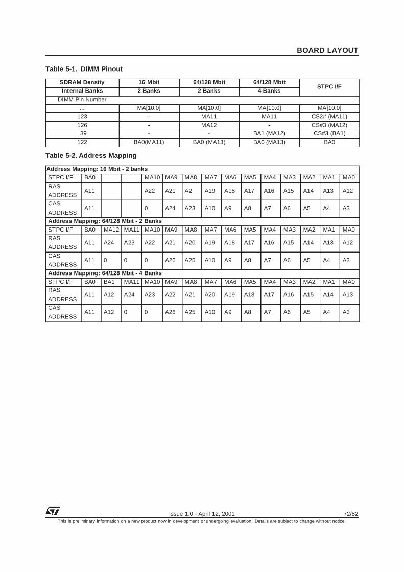
BOARD LAYOUT
Issue 1.0 - April 12, 2001 72/82This is preliminary information on a new product now in development or undergoing evaluation. Details are subject to change without notice.
Table 5-1. DIMM Pinout
SDRAM Density 16 Mbit 64/128 Mbit 64/128 MbitSTPC I/F
Internal Banks 2 Banks 2 Banks 4 BanksDIMM Pin Number
... MA[10:0] MA[10:0] MA[10:0] MA[10:0]123 - MA11 MA11 CS2# (MA11)
126 - MA12 - CS#3 (MA12)39 - - BA1 (MA12) CS#3 (BA1)
122 BA0(MA11) BA0 (MA13) BA0 (MA13) BA0
Table 5-2. Address Mapping
Address Mapping: 16 Mbit - 2 banksSTPC I/F BA0 MA10 MA9 MA8 MA7 MA6 MA5 MA4 MA3 MA2 MA1 MA0
RAS
ADDRESSA11 A22 A21 A2 A19 A18 A17 A16 A15 A14 A13 A12
CAS
ADDRESSA11 0 A24 A23 A10 A9 A8 A7 A6 A5 A4 A3
Address Mapping: 64/128 Mbit - 2 BanksSTPC I/F BA0 MA12 MA11 MA10 MA9 MA8 MA7 MA6 MA5 MA4 MA3 MA2 MA1 MA0
RAS
ADDRESSA11 A24 A23 A22 A21 A20 A19 A18 A17 A16 A15 A14 A13 A12
CAS
ADDRESSA11 0 0 0 A26 A25 A10 A9 A8 A7 A6 A5 A4 A3
Address Mapping: 64/128 Mbit - 4 BanksSTPC I/F BA0 BA1 MA11 MA10 MA9 MA8 MA7 MA6 MA5 MA4 MA3 MA2 MA1 MA0RAS
ADDRESSA11 A12 A24 A23 A22 A21 A20 A19 A18 A17 A16 A15 A14 A13
CAS
ADDRESSA11 A12 0 0 A26 A25 A10 A9 A8 A7 A6 A5 A4 A3

BOARD LAYOUT
73/82 Issue 1.0 - April 12, 2001This is preliminary information on a new product now in development or undergoing evaluation. Details are subject to change without notice.

MECHANICAL DATA
Issue 1.0 - April 12, 2001 74/82This is preliminary information on a new product now in development or undergoing evaluation. Details are subject to change without notice.
6. MECHANICAL DATA
6.1 516-Pin Package Dimension
The pin numbering for the STPC 516-pin PlasticBGA package is shown inFigure 6-1.
Dimensions are shown in Figure 6-2, Table 6-1and Figure 6-3, Table 6-2.
Figure 6-1. 516-Pin PBGA Package - Top View
A
B
D
E
F
G
H
J
K
L
M
N
P
R
T
U
V
W
Y
AA
AB
AC
AD
AE
AF
C
1 3 5 7 9 11 13 15 17 19 21 23 25
2 4 6 8 10 12 14 16 18 20 22 24 26
A
B
D
E
F
G
H
J
K
L
M
N
P
R
T
U
V
W
Y
AA
AB
AC
AD
AE
AF
C
1 3 5 7 9 11 13 15 17 19 21 23 25
2 4 6 8 10 12 14 16 18 20 22 24 26

MECHANICAL DATA
75/82 Issue 1.0 - April 12, 2001This is preliminary information on a new product now in development or undergoing evaluation. Details are subject to change without notice.
Figure 6-2. 516-pin PBGA Package - PCB Dimensions
Table 6-1. 516-pin PBGA Package - PCB Dimensions
Symbolsmm inches
Min Typ Max Min Typ MaxA 34.80 35.00 35.20 1.370 1.378 1.386
B 1.22 1.27 1.32 0.048 0.050 0.052
C 0.60 0.76 0.90 0.024 0.030 0.035D 1.57 1.62 1.67 0.062 0.064 0.066
E 0.15 0.20 0.25 0.006 0.008 0.001F 0.05 0.10 0.15 0.002 0.004 0.006
G 0.75 0.80 0.85 0.030 0.032 0.034
A
A
B
Detail
A1 Ball Pad Corner
D
F
E
GC

MECHANICAL DATA
Issue 1.0 - April 12, 2001 76/82This is preliminary information on a new product now in development or undergoing evaluation. Details are subject to change without notice.
Figure 6-3. 516-pin PBGA Package - Dimensions
Table 6-2. 516-pin PBGA Package - Dimensions
Symbolsmm inches
Min Typ Max Min Typ Max
A 0.50 0.56 0.62 0.020 0.022 0.024B 1.12 1.17 1.22 0.044 0.046 0.048
C 0.60 0.76 0.92 0.024 0.030 0.036D 0.52 0.53 0.54 0.020 0.021 0.022
E 0.63 0.78 0.93 0.025 0.031 0.037
F 0.60 0.63 0.66 0.024 0.025 0.026G 30.0 11.8
A
B
C
Solderball Solderball after collapse
D
E
F
G

MECHANICAL DATA
77/82 Issue 1.0 - April 12, 2001This is preliminary information on a new product now in development or undergoing evaluation. Details are subject to change without notice.
6.2 516-Pin Package Thermal Data
516-pin PBGA package has a Power DissipationCapability of 4.5W which increases to 6W whenused with a Heatsink.
The structure in shown inFigure 6-4.
Thermal dissipation options are illustrated inFig-ure 6-5 and Figure 6-6.
Figure 6-4. 516-Pin PBGA Structure
Thermal balls
Power & Ground layersSignal layers
Figure 6-5. Thermal Dissipation Without Heatsink
Ambient
Case
Junction
Board
Ambient
Ambient
Case
Junction
Board
Rca
Rjc
Rjb
Rba
6 6
1258.5
Rja = 13 °C/WAirflow = 0
Board dimensions:
The PBGA is centred on board
Copper thickness:- 17µm for internal layers- 34µm for external layers
- 10.2 cm x 12.7 cm- 4 layers (2 for signals, 1 GND, 1VCC)
There are no other devices1 via pad per ground ball (8-mil wire)40% copper on signal layers
Board temperature taken at the centre balls
Board

MECHANICAL DATA
Issue 1.0 - April 12, 2001 78/82This is preliminary information on a new product now in development or undergoing evaluation. Details are subject to change without notice.
Figure 6-6. Thermal Dissipation With Heatsink
Ambient
Case
Junction
Board
Ambient
Ambient
Case
Junction
Board
Rca
Rjc
Rjb
Rba
3 6
508.5
Rja = 9.5 °C/WAirflow = 0
Board dimensions:
The PBGA is centred on board
Copper thickness:- 17µm for internal layers- 34µm for external layers
- 10.2 cm x 12.7 cm- 4 layers (2 for signals, 1 GND, 1VCC)
There are no other devices
Heat sink is 11.1°C/W
1 via pad per ground ball (8-mil wire)40% copper on signal layers
Board temperature taken at the centre balls
Board
MECHANICAL DATA
79/82 Issue 1.0 - April 12, 2001This is preliminary information on a new product now in development or undergoing evaluation. Details are subject to change without notice.

ORDERING DATA
Issue 1.0 - April 12, 2001 80/82This is preliminary information on a new product now in development or undergoing evaluation. Details are subject to change without notice.
7 ORDERING DATA
7.1 ORDERING CODES
ST PC I2 E E Y C
STMicroelectronics
Prefix
Product Family
PC: PC Compatible
Product ID
A1: Atlas
Core Speed
E: 100 MHz
H: 133 MHz
Memory Speed
D: 90 MHz
E: 100 MHz
Package
Y: 516 Overmoulded BGA
Temperature Range
C: CommercialTcase = 0 to +85°C
I: IndustrialTcase = -40 to +115°C
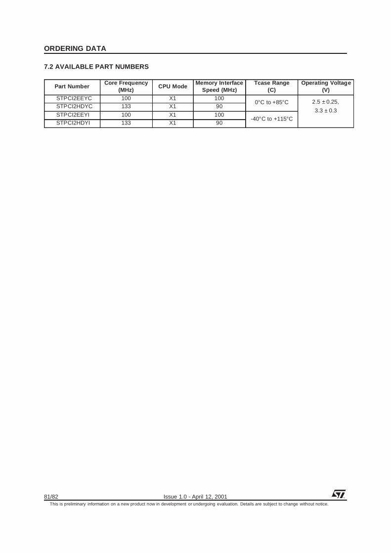
ORDERING DATA
81/82 Issue 1.0 - April 12, 2001This is preliminary information on a new product now in development or undergoing evaluation. Details are subject to change without notice.
7.2 AVAILABLE PART NUMBERS
Part NumberCore Frequency
(MHz)CPU Mode
Memory InterfaceSpeed (MHz)
Tcase Range(C)
Operating Voltage(V)
STPCI2EEYC 100 X1 1000°C to +85°C 2.5 ± 0.25,
3.3 ± 0.3STPCI2HDYC 133 X1 90
STPCI2EEYI 100 X1 100-40°C to +115°C
STPCI2HDYI 133 X1 90

Information furnished is believed to be accurate and reliable. However, STMicroelectronics assumes no responsibility for the consequencesof use of such information nor for any infringement of patents or other rights of third parties which may result from its use. No license is grantedby implication or otherwise under any patent or patent rights of STMicroelectronics. Specifications mentioned in this publication are subjectto change without notice. This publication supersedes and replaces all information previously supplied. STMicroelectronics products are notauthorized for use as critical components in life support devices or systems without express written approval of STMicroelectronics.
2000 STMicroelectronics - All Rights Reserved
The ST logo is a registered trademark of STMicroelectronics.
All other names are the property of their respective owners.
STMicroelectronics GROUP OF COMPANIES
Australia - Brazil - China - France - Germany - Italy - Japan - Korea - Malaysia - Malta - Mexico - Morocco - The Netherlands - Singapore -Spain - Sweden - Switzerland - Taiwan - Thailand - United Kingdom - U.S.A.
82Issue 1.0
This is preliminary information on a new product now in development or undergoing evaluation. Details are subject to change without notice.
Related Documents