Workshop Department of Physics, University of Ulsan– IPCMS October 9 th 2017 000 LIA Franco-Coréen Functional nanostructures : morphology, nanoelectronics and ultrafast optics

Welcome message from author
This document is posted to help you gain knowledge. Please leave a comment to let me know what you think about it! Share it to your friends and learn new things together.
Transcript

Workshop
Department of Physics, University of
Ulsan– IPCMS
October 9th 2017
000
LIA Franco-Coréen Functional nanostructures : morphology, nanoelectronics and ultrafast optics


PROGRAM
Monday, October 9th
9h00-9h30
S. Haacke
Welcome and general presentation of IPCMS
9h30-10h00
S.C. Hong
Accomplishment for the last 8 years at Energy Harvest-Storage Research Center of University of
Ulsan
10h00-10h30
A. Dinia
Functionalized this films oxides for photon conversion and photovoltaic solar cells
10h30-11h00 Break
11h00-11h30
Y.H. Shin
Computational evaluations of energy-harvesting and energy-storing nanocomposite materials
11h30-12h00
M. Boero
Simple but efficient method for inhibiting sintering of catalytic Pt nano-clusters on metal-oxide
support
12h00-13h30 Lunch
13h30-14h00
L. Limot
Molecular spin coupling at the tip of a STM
14h00-14h30
J. Kim
STM study on the layered chalcogenide materials
14h30-15h00
B. Donnio
Ligand-Directed Self-Assembly Of Nanoparticles

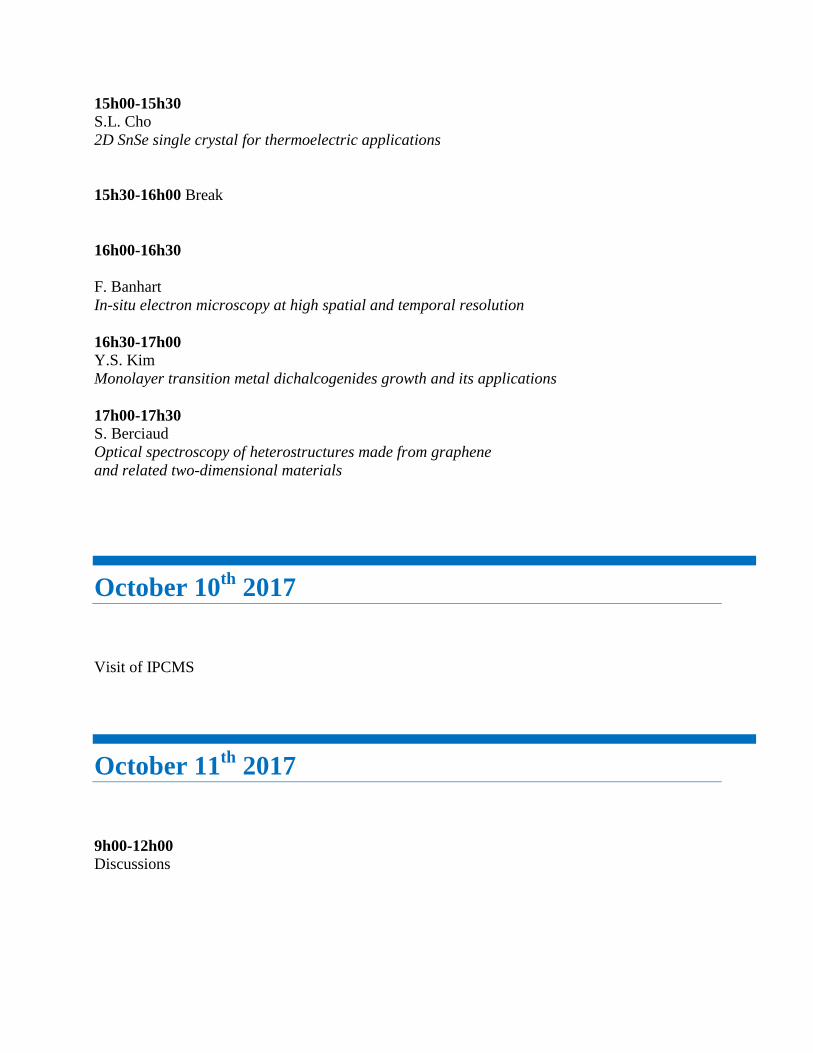
15h00-15h30
S.L. Cho
2D SnSe single crystal for thermoelectric applications
15h30-16h00 Break
16h00-16h30
F. Banhart
In-situ electron microscopy at high spatial and temporal resolution
16h30-17h00
Y.S. Kim
Monolayer transition metal dichalcogenides growth and its applications
17h00-17h30
S. Berciaud
Optical spectroscopy of heterostructures made from graphene
and related two-dimensional materials
October 10th
2017
Visit of IPCMS
October 11th
2017
9h00-12h00
Discussions

Prof. Stefan Haacke
University of Strasbourg
Institut de Physique et Chimie des Matériaux de Strasbourg, UMR 7504,
67000 Strasbourg, France
E-mail: [email protected]
Homepage: http://www.ipcms.unistra.fr/?page_id=6777&lang=en
Telephone: +33-3-88-10-71-71
Experience
2013.01- 2017.12 Director, IPCMS
2004.09 - present Professor, University of Strasbourg
1999.09-2004.08 Assistant Professor, University & Swiss Fed. Inst. of Technology
Lausanne
1994.02 – 1999.08 Research Assistant, Swiss Fed. Inst. of Technology Lausanne
Education
1990.09-1994.01 Ph.D., J. Fourier University Grenoble (France)
1988.09-1990.07 M.S., Physics; Technical University Berlin
1986.09-1988.07 B.S., J. Fourier University Grenoble (France)
Research Topics
1. Instrumentation for ultrafast spectroscopy
2. Primary photochemical processes in retinal proteins and biomimetic systems
3. Ultrafast photophysics of molecles and nanostructures for energy conversion
Selected Publications
1. Full account on http://www.researcherid.com/rid/B-5554-2013
2. "Simultaneously enhancing dissociation and suppressing recombination in perovskite solar
cells", P.-Y. Lin, T. Wu, M. Ahmadi, Li Liu, S. Haacke, T.-F. Guo, Bin Hu, Nano Energy (2017),
36, 95-101.
3. "A new record excited state 3MLCT lifetime for metalorganic Fe(II) complexes", L. Liu, T.
Duchanois, T. Etienne, A. Monari, M. Beley, X. Assfeld, S. Haacke, P.C. Gros, Phys. Chem.
Chem. Phys., 18, 12550 (2016)
4. "Controlling Charge Separation and Recombination by Chemical Design in Donor-Acceptor
Dyads", L. Liu, P. Eisenbrandt, T. Roland, M. Polkehn, P.-O. Schwartz, A. Ruff, S. Ludwigs, N.
Leclerc, E. Zaborova, J. Léonard, S. Méry, I. Burghardt, S. Haacke, Phys. Chem. Chem. Phys.,
18, 18536 - 18548 (2016);
5. "2 MHz tunable non collinear optical parametric amplifiers with pulse durations down to 6 fs",
J. Nillon, O. Crégut, C. Bressler and S. Haacke, Optics Express, 22, 14964-14974 (2014).
6. “Probing the Ultrafast Charge Translocation of Photoexcited Retinal in Bacteriorhodopsin”, S.
Schenkl, F.van Mourik, G. van der Zwan, S. Haacke, M. Chergui, Science, 2005, 309, 917-921.

Interdisciplinary Research at Strasbourg Institute of Physics and Chemistry of
Materials
Stefan Haacke
Director Strasbourg Institute of Physics and Chemistry of Materials (IPCMS)
University of Strasbourg
The Strasbourg Institute of Physics and Chemistry of Materials (IPCMS, [1]) is an
interdisciplinary research centre, with a total staff of 230 people, jointly run by the CNRS and the
University of Strasbourg. IPCMS brings together physicists and chemists, whose core of research
is on the design of molecules, inorganic solids, nanostructures and thin films, and the
investigation of these materials from the nano- to the macroscale, with particular attention to their
functional properties and/or new fundamental science they may exhibit.
The scientific priorities and international recognition of IPCMS lie in the areas of i) the
controlled design of molecular edifices & nanostructures including their self-organisation, ii)
nano-magnetism & magneto-electric coupling, iii) spintronics and nano-electronics, iv) ultrafast
processes in condensed matter, v) electron and scanning tunnneling microscopy, and vi) new
nanomaterials for health & energy conversion applications. Strongly interlaced with notorious
national and international partners from academia and industry, our strategy over the last years
was to strengthen our position as an internationnally renowned institute for interdisciplinay
nanoscience covering fundamental and applicative research for innovations in communication
technologies, health and energy.
The recent French excellence initiative PIA has brought three new priority programs to IPCMS,
since the institute is in charge of the excellence cluster Labex NIE, and is laureate of the two
Equipex projects UNION (in coll. with ISIS) and UTEM.
[1] http://www.ipcms.unistra.fr/?lang=en

Prof. Soon Cheol Hong
Computational Physics Laboratory
Department of Physics, University of Ulsan
93 Daehak-ro, Nam-gu, Ulsan 44610, Republic of Korea
E-mail: [email protected]
Telephone: +82-52-259-23231
Experience
2017.01-present Editor-in-Chief, Physics & High Technology (published by the Korean
Physical Society)
2009.09-present Director, Energy Harvest-Storage Research Center, University of Ulsan
1982.03-present Professor, University of Ulsan
1979.03-1982.02 Researcher, Korea Institute of Machinery and Metals
2015.01-2016.12 Editor-in-Chief, Journal of Magnetics (published by the Korean
Magnetic Society
Education
1988. 08 Ph.D., Northwestern University
1979. 02 M.S., KAIST
1977.02 B.S., Pusan National University
Research Topics
Surface magnetism, magnetostriction, and magnetocrystalline anisotropy using first principle
calculation
Selected Publications
1. S. W. Han, Y. H. Hwang, S.-H. Kim, W. S. Yun, J. D. Lee, M. G. Park, S. Ryu, J. S. Park,
D.-H. Yoo, S.-P. Yoon, S. C. Hong, K. S. Kim, and Y. S. Park, "Controlling Ferromagnetic
Easy Axis in a Layered MoS2 Single Crystal", Phys. Rev. Lett. 110, 247201 (2013). Cited 53
times.
2. W. S. Yun, S. W. Han, S. C. Hong, I. G. Kim, and J. D. Lee, "Thickness and strain effects on
electronic structures of transition metal dichalcogenides: 2H-MX2 semiconductors (M = Mo,
W; X = S, Se, Te) ", Phys. Rev. B 85, 033305 (2012). Cited 498 times
3. S. C. Hong, A. J. Freeman, and C. L. Fu, "Structural, electronic, and magnetic properties of
clean and Ag-covered Fe monolayers on W (110)", Phys. Rev. B 38, 12156 (1988). Cited
105 times.
4. S. C. Hong, J. I. Lee, and R. Wu, "Ferromagnetism in Pd thin films induced by quantum well
states", Phys. Rev. B 75, 172402(2007). Cited 40 times
Awards
2001 The Year Professor of University of Ulsan
2007 Research Excellency Award given by Korean Magnetic Society
2015 Changsung Award given by Korean Magnetic Society

Accomplishment for the last 8 years at Energy Harvest-Storage Research
Center of University of Ulsan
Soon Cheol Hong
Energy Harvest-Storage Research Center and Department of Physics, University of Ulsan
In this presentation I will introduce Energy Harvest-Storage Research Center, focusing on what we have
accomplished for the last 8 years. The center has been supported since 2009 by Ministry of Education of
Korea. Our main research interests are search for desirable renewable energy materials of solar cell,
thermoelectricity, piezoelectricity, and magnetostriction.
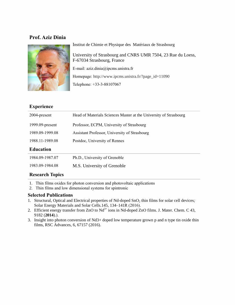
Prof. Aziz Dinia
Institut de Chimie et Physique des Matériaux de Strasbourg
University of Strasbourg and CNRS UMR 7504, 23 Rue du Loess,
F-67034 Strasbourg, France
E-mail: [email protected]
Homepage: http://www.ipcms.unistra.fr/?page_id=11090
Telephone: +33-3-88107067
Experience
2004-present
1999.09-present
Head of Materials Sciences Master at the University of Strasbourg
Professor, ECPM, University of Strasbourg
1989.09-1999.08 Assistant Professor, University of Strasbourg
1988.11-1989.08 Postdoc, University of Rennes
Education
1984.09-1987.07 Ph.D., University of Grenoble
1983.09-1984.08 M.S. University of Grenoble
Research Topics
1. Thin films oxides for photon conversion and photovoltaic applications
2. Thin films and low dimensional systems for spintronic
Selected Publications 1. Structural, Optical and Electrical properties of Nd-doped SnO2 thin films for solar cell devices;
Solar Energy Materials and Solar Cells.145, 134–141R (2016).
2. Efficient energy transfer from ZnO to Nd3+
ions in Nd-doped ZnO films. J. Mater. Chem. C 43,
9182 (2014).).
3. Insight into photon conversion of Nd3+ doped low temperature grown p and n type tin oxide thin
films, RSC Advances, 6, 67157 (2016).

Functionalized this films oxides for photon conversion and photovoltaic solar
cells
M. Balestrieria, K. Bouras
b, K. Yassaroglu
a, G. Schmerber
a, Gérald Ferblantier
b, Silviu Colis
a, J.
L. Rehspringera, Thomas Fix
b, Abdelilah Slaoui
b and Aziz Dinia
a,
a University of Strasbourg, Institut de Physique et Chimie des Matériaux de Strasbourg
(IPCMS),CNRS UMR 7504, 23 rue du Loess, F-67034 Strasbourg, France b University of Strasbourg, ICube, CNRS UMR 7357, 23 rue du Loess, BP 20 CR, 67037
Strasbourg Cedex 2, France
The synthesis of functional high-quality oxide thin films is a major current research challenge
given their potential applications in electronic (flat panel displays, flexible electronics) and
optoelectronic (LEDs, photovoltaic) sectors. In particular, transparent conducting oxides (TCOs)
are of great interest for solar cells.
Herein, we first report on fabrication and characterization of rare earth (RE) doped TCOs such as
ZnO, SnOx or CeOx. The structural, optical and electrical properties of such functionalized
oxides will be thoroughly presented. An efficient energy transfer from the RE ions to the host
matrix will be presented. The down shifting process will be demonstrated through the conversion
of UV photons to infrared ones, which is favorable for reducing the thermalization losses in solar
cells.
In a second part, we will quickly report on some alternative materials for solar cells. First the
synthesis of a new class of ferroelectric oxide films that has high photons absorption and a
moderate bandgap, making them very suitable for photovoltaic applications. Second on halide
perovskite, CH3NH3PbI3, that emerged as a light harvester. The power-conversion efficiency of
halide perovskite solar cells has soared up to 22.1%[1]
earlier this year.
Prof. Young-Han Shin
Multiscale Materials Modeling Lab.
Department of Physics, University of Ulsan
93 Daehak-ro, Nam-gu, Ulsan 44610, Republic of Korea
E-mail: [email protected]
Homepage: http://may.ulsan.ac.kr/M3L
Telephone: +82-52-259-1027
Experience
2009.09-present Professor, University of Ulsan
2006.09-2009.08 Research Professor, POSTECH
2001.09-2006.08 Postdoc, University of Pennsylvania, Sejong Univ.
Education
1996.03-2001.08 Ph.D., KAIST
1994.03-1996.02 M.S., KAIST
1990.03-1994.02 B.S., Yonsei University
Research Topics
1. Theoretical modeling of materials with functional properties such as ferroelecrics,
piezoelectrics, thermoelectrics, etc.
2. Multiscale computational approaches
Selected Publications
1. bdus Samad, Young-Han Shin, Mo2@VS2 nanocomposite as a superior hybrid anode material.
ACS Applied Materials & Interfaces 9, 29942-29949 (2017).
2. Aamir Shafique, Abdus Samad, Young-Han Shin, Ultra low lattice thermal conductivities and
carrier mobilities of single SnX2 (X=Se,S): a first principles study. Physical Chemistry Chemical
Physics 19, 20677-20683 (2017).
3. Abdus Samad, Aamir Shafique, Hye Jung Kim,and Young-Han Shin, Superionic and electronic
conductivity in monolayer W2C: ab initio predictions. Journal of Materials Chemistry A 5,
11094-11099 (2017).
4. Abdus Samad, Aamir Shafique, and Young-Han Shin, Adsorption and diffusion of mono, di, and
trivalent ions on two-dimensional TiS2. Nanotechnology 28, 175401 (2017).
5. Aamir Shafique and Young-Han Shin, Thermoelectric and phonon transport properties of two-
dimensional IV-VI compounds. Scientific Reports 7, 506 (2017).
6. Abdus Samad, Mohammad Noor-A-Alam, Young-Han Shin, First principles study of
SnS2/graphene heterostructure: a promising anode material for rechargeable Na ion batteries.
Journal of Materials Chemistry A 4, 14316-14323 (2016).
7. Mohammad Noor-A-Alam, Young-Han Shin, Switchable polarization in an unzipped graphene
oxide monolayer. Physical Chemistry Chemical Physics 18, 20443-20449 (2016).
8. Mohammad Noor-A-Alam, Hye Jung Kim, Young-Han Shin, Hydrogen and fluorine co-
decorated silicene: A first principles study of piezoelectric properties. Journal of Applied
Physics 117, 224304 (2015).

Computational evaluations of energy-harvesting and energy-storing
nanocomposite materials
Young-Han Shin
Department of Physics, University of Ulsan, Ulsan 44610, Korea
Nowadays people easily bring several electronic devices while traveling in a short or long
distance. To make them self-powered, external energy sources such as light, wind, heat might be
considered to store their energy in secondary batteries. Depending on the external stimuli, the
best responding physical properties can be chosen to find corresponding materials.
Computational evaluations of these physical properties can help develop future energy materials.
In addition to the energy-harvesting materials, the development of materials is also required for
storing energy. In this presentation, I am going to show a series of researches in my research
group on the piezoelectric, thermoelectric properties of low-dimensional materials as well as the
ionic transport on top of the surface of the materials. Especially we focus on the two-dimensional
materials such as graphene, h-BN, silicene, SnSe, SnS, GeSe, GeS, SnS2, TiS2, MoS2, VS2. For
using as solid electrolyte, the structural properties of antiperovskite Na3OCl will be also
mentioned. Most results were obtained from first-principles calculations.
Two physical properties (piezoelectricity and thermoelectricity) for energy harvest that are obtained from
total energy calculations. (a) Piezoelectricity of chair hydrogenated or fluorinated h-BN, (b) lattice thermal
conductivity of monolayer SnSe2
Mauro Boero
Institut de Chimie et Physique des Matériaux de Strasbourg
University of Strasbourg and CNRS UMR 7504, 23 Rue du Loess,
F-67034 Strasbourg, France
E-mail: [email protected]
Homepage: http://www.ipcms.unistra.fr/?page_id=11090
Telephone: +33-3-88107142
Experience
2008.12-present Research Director, IPCMS University of Strasbourg-CNRS, France
Scientific director of the HPC Mesocenter Equip@Meso, Strasbourg
Visiting Full Professor, The University of Tokyo, Japan
2001.09-2008.11 Associate Professor, University of Tsukuba, Japan
1998.05-2001.08 Research Fellow, AIST Tsukuba, Japan
1996.07-1998.04 Postdoc, Max-Planck Institut für Festkörperforschung, Stuttgatr, Germany
1995.07-1996.06 Postdoc, IBM Research Laboratory, Zurich, Switzerland
1994.09-1995.06 Postdoc, Swiss Federal Institute of Technology in Lausanne (EPFL),
Switzerland
Education
1991.09-1994.08 Ph.D., University of Torino (Italy) and EPFL Lausanne (Switzerland)
1989 “Laurea cum laude.” in physics, University of Turin (Italiy),
Research Topics
1. Molecular modeling in materials sciences and biosciences
2. Computational approaches and massively parallel computing
Recent Selected Publications
1. A. Amokrane, S, Klyatskaya M. Boero, M. Ruben, J-P. Bucher, ACS Nano (accepted).
2. K. Koizumi, K. Nobusada M. Boero, Phys. Chem. Chem. Phys. 19, 3498 (2017) – cover issue
3. K. Koizumi, K. Nobusada M. Boero , Chemistry Eur. J. 23, 1531 (2017) – frontispiece
4. K. Koizumi, K. Nobusada M. Boero, Chemistry Eur. J. 22, 5181 (2016) – cover issue

Simple but efficient method for inhibiting sintering of catalytic Pt nano-
clusters on metal-oxide support
Kenichi Koizumi1,2*
, Katsuyuki Nobusada1,2
, and Mauro Boero3,41,*
1 Department of Theoretical and Computational Molecular Science, Institute for Molecular
Science, Myodaiji, Okazaki 444-8585, Japan 2 Elements Strategy Initiative for Catalysts and Batteries (ESICB), Kyoto University, Katsura,
Kyoto 615-8520, Japan 3 University of Strasbourg, Institut de Physique et Chimie des Matériaux de Strasbourg
(IPCMS),CNRS UMR 7504, 23 rue du Loess, F-67034 Strasbourg, France 4Computational Materials Science Initiative (CMSI) Post-K Project, Dept. of Applied Physics,
University of Tokyo, Hongo, Tokyo (Japan)
*Corresponding author: [email protected]
The sintering is a major source of concern in precious metals nano-catalysts since it induces the
formation of large nanoparticles and particles with negative consequences on the accessible
active surface of the catalyst. We propose a simple and efficient method to inhibit aggregation
and sintering of Pt clusters supported on metal-oxide. Our proposed workaround allows to solve
this problem and preserves the accessible catalytic surface even at relatively high temperatures
(~700 K), as the ones expected to experience by this class of catalytic systems. The key idea is
the inclusion of transition metal atoms, such as Ni, into the Pt clusters. Ni atoms, in turn, realize
an anchoring via the formation of strong chemical bonds with oxygen atoms present in the typical
metal–oxide support. To elucidate the efficiency of the method, we use first-principles molecular
dynamics enhanced with free-energy sampling methods. To this aim, we introduce a specific
reaction coordinate to control the average coordination number of each cluster insensitive to
periodic boundary conditions routinely adopted in this type of simulations. This allows for a
precise description of the sintering processes and for an accurate estimation of the related free-
energy barriers for aggregations. These virtual experiments show how doped Ni atoms, having a
stronger affinity to O than Pt, anchor tightly the Pt nanocluster to the metal-oxide supports and
inhibit the tendency of these clusters to aggregate on the support.

Dr. Laurent Limot
Institut de Physique et Chimie des Matériaux de Strasbourg
Université de Strasbourg, CNRS, IPCMS, UMR 7504, F-67000
Strasbourg, France
E-mail: [email protected]
http://www-ipcms.u-strasbg.fr/stmipcms/
Telephone: +33-388-10-70-22
Experience
2006.10-present CNRS Researcher
2006.03-2006.09 Postdoc, Université de Strasbourg, CNRS
2001.01-2006.02 Postdoc, Kiel University
Education
1997.10-2000.12 Ph.D., Laboratoire de Physique des Solides, Université Parsi-Sud
1995.10-1997.07 M.S., Université Parsi-Sud
1992.10-1995.07 B.S., Université Parsi-Sud
Research Topics
1. Electronic and spin-polarized transport across single atoms and molecules, molecular
magnetism, surface magnetism
2. Techniques: Scanning Tunneling Microscopy (STM) and Spectroscopy (STS), Inelastic Electron
Tunneling Spectroscopy (IETS), Spin-Polarized STM (SP-STM)
Selected Publications
1. Controlled spin switch in a metallocene molecular junction, Nature Commun. (accepted)
2. Efficient spin-flip excitation of a nickelocene molecule, Nano Lett. 17, 1877 (2017)
3. Kondo resonance of a Co atom exchange coupled to a ferromagnetic tip, Nano Lett. 16, 6298
(2016)

Molecular spin coupling at the tip of a STM
M. Ormaza
1, P. Abufager
2, B. Verlhac
1, N. Bachellier
1, M.-L. Bocquet
3, N. Lorente
4, and Laurent Limot
1,*
1Université de Strasbourg, CNRS, IPCMS, UMR 7504, F-67000 Strasbourg, France
2Instituto de Física de Rosario, CONICET, Universidad Nacional de Rosario, Argentina
3Ecole Normale Supérieure, UPMC Univ. Paris 06, CNRS, 75005 Paris, France
4CFM/MPC and DIPC, 20018 Donostia-San Sebastián, Spain
Recent advances in addressing and controlling the spin states of a surface-supported object (atom
or molecule) have further accredited the prospect of quantum computing and of an ultimate data-
storage capacity [1]. Information encoding requires that the object must possess stable magnetic
states, in particular magnetic anisotropy to yield distinct spin-dependent states in the absence of a
magnetic field together with long magnetic relaxation times. Scanning probe techniques have
shown that inelastic electron tunneling spectroscopy (IETS) within the junction of a scanning
tunneling microscope (STM) is a good starting point to study the stability of these spin states [2].
STM-IETS allows for an all-electrical characterization of these states by promoting and detecting
spin-flip excitations within the object of interest. It can also provide an electrical control over
them, simplifying the information readout process. As spin excitations need however to be
preserved from scattering events with itinerant electrons, single objects are usually placed on
non-metallic surfaces such as thin-insulating layers or superconductors.
In this sense, new approaches to improve the detection of spin-flip excitations are desirable. With
this purpose we present here a novel strategy based on the molecular functionalization of a STM
tip. We study the surface magnetism of a simple double-decker molecule, nickelocene
[Ni(C5H5)2], which is adsorbed directly on a copper surface. By means of X-ray magnetic circular
dichroism and density functional theory calculations, we show that nickelocene on the surface is
magnetic (Spin = 1) and possesses a uniaxial magnetic anisotropy, while IETS reveals an
exceptionally efficient spin-flip excitation occurring in the molecule [3]. Interestingly,
nickelocene preserves its magnetic moment and magnetic anisotropy not only on the surface, but
also in different metallic environments. Taking advantage of this robustness, we are able to
functionalize the STM tip with a nickelocene, which can then be employed as a portable source
of inelastic excitations. As we will show during the talk, IETS can then be used to probe the
interaction between a surface-supported object and the nickelocene tip, including a magnetic
interaction.
References
[1] T. Choi et al., Nat. Nanotech. 6 (2017)
[2] C.F. Hirjibehedin et al., Science 312, 1021 (2006)
[3] M. Ormaza et al., Nano Lett. 17, 1877 (2017)

Graphical Abstract (1 Figure)
The center panel sketches the STM setups employed. With a metal tip, IETS reveals an
exceptionally efficient spin-flip excitation for nickelocene adsorbed on a copper surface. Intense
stepped-like features symmetric relative to zero-bias are in fact detected at ±3.2 meV in the
tunneling spectrum (left panel). This energy corresponds to the uniaxial magnetic anisotropy of
nickelocene, in other words below 3.2 meV the magnetic moment of the molecule is parallel to
the aromatic rings, while above 3.2 meV the magnetic moment is along the principal molecular
axis. Interestingly, the molecule preserves its magnetic moment and magnetic anisotropy in
different metallic environments. By taking advantage of this property, we are able to
functionalize the STM tip with a nickelocene molecule. Such a tip can then be employed as a
portable source of inelastic excitations and used to produce, for example, a double spin-flip
excitation (right panel).

Prof. Jungdae Kim
Nanoscale Surface Science Laboratory
Department of Physics, University of Ulsan
93 Daehak-ro, Nam-gu, Ulsan 44610, Republic of Korea
E-mail: [email protected]
Homepage: https://sites.google.com/site/nsslab6789/home
Telephone: +82-52-259-2324
Experience
2016.09-present Associate Professor, University of Ulsan
2012.09-2016.08 Assistant Professor, University of Ulsan
2011.05-2012.08 Postdoc, Brookhaven National Lab
2010.09-2011.04 Postdoc, University of Texas at Austin
Education
2004.09-2010.08 Ph.D., University of Texas at Austin
2001.03-2003.02 M.S., Seoul National University
1994.03-2000.08 B.S., Pusan National University
Research Topics
1. Surface science using home-built scanning tunneling microscope (STM)
2. 2D layered chalcogenide materials
Selected Publications
1. Revealing the origin of p-type characteristics in a SnSe single crystal. Appl. Phys. Lett.
(accepted).
2. Achieving ZT=2.2 with Bi-doped n-type SnSe single crystals. Nat. Commun. 7, 13713 (2016).
3. A microscopic study investigating the structure of SnSe surfaces. Surf. Sci. 651, 5 (2016).

STM study on the layered chalcogenide materials
Ganbat Duvjir1, Trinh Thi Ly
1, Sunglae Cho
1, Young Jun Chang
2, Jaekwang Lee
3, and Jungdae Kim
1,*
1Department of Physics, BRL, and EHSRC, University of Ulsan, Ulsan 44610, Korea
2Department of Physics, University of Seoul, Seoul 02504, Korea
3Department of Physics, Pusan National University, Busan 46241, Korea
*Corresponding author: [email protected]
Layered chalcogenide materials (LCMs) have been intensively studied due to their versatile
physical properties when prepared in a few monolayer thicknesses. Weak van der Waals coupling
between layers allows simple mechanical exfoliation to fabricate two-dimensional LCMs.
Scanning tunneling microscopy/spectroscopy (STM/S) is an ideal probe to investigate the
microscopic nature of materials at the atomic scale. In this presentation, recent STM studies on
SnSe, SnSe1-xSx will be discussed. SnSe is a IV-VI semiconductor with a band gap of ~1.0 eV.
Recently, Zhao et al. [Nature 508, 373 (2014)] reported the ultra-high thermoelectric performance
of SnSe single crystal with a maximum ZT = S2σT/κ (figure of merit) value of 2.6 at 923 K,
where S is the Seebeck coefficient, σ is the electrical conductivity, κ it the thermal conductivity,
and T is the absolute temperature. Although this high ZT value has attracted considerable
attention, the microscopic origin of p-type character of SnSe has yet to be clearly understood.
Here, we directly observed and identified intrinsic point defects existing on the SnSe via home-
built STM, and investigated the role of defects on the electronic properties using density
functional theory (DFT) calculations. In addition, we investigate the structural evolution of
crystalline SnSe1-xSx on the atomic scale by combining STM measurement with DFT
calculations. If time is allowed, interesting structural changes on monolayer VSe2 will be
discussed at the end of presentation.

Pictures of home-built low temperature scanning tunneling microscope (STM) system in Nanoscale
Surface Science Lab (Prof. Jungdae Kim).


Dr Bertrand DONNIO
Institut de Physique et Chimie des Matériaux de Strasbourg
UMR7504 CNRS-University of Strasbourg
E-mail: [email protected]
Homepage: http://www.ipcms.unistra.fr/?page_id=25889&lang=en
Telephone: +33 (0)688107156
Experience
2015.09-present DR CNRS, CNRS-University of Strasbourg
2013.01-2015.08 DR CNRS, COMPASS-SOLVAY-UPENN
2010.10-2012.12 DR CNRS, CNRS-University of Strasbourg
1999.10-2010.10 CR CNRS, CNRS-University of Strasbourg
1996.03-1999.10 PDF (U. Neuchâtel-CH, U. Exeter-UK, U. Freiburg-D)
Education
2009.02 HDR., University of Strasbourg, F
1992.09-1996.02 PhD, University of Sheffield, UK
1992.09-1996.09 MS, University of Rennes, F
Research Topics
1. Supramolecular chemistry, liquid crystal self-assembly
2. Synthesis (oligomeric molecules, dendrons & dendrimers, coordination metal complexes, ..)
3. Functionalization and self-assembly of nanoparticles
Selected Publications
[1] D. Jishkariani, et al. J. Am. Chem. Soc. 2015 137 10728−10734.
[2] B. T. Diroll, et al. J. Am. Chem. Soc. 2016 138 10508-10515.
[3] B. T. Diroll, et al. Nano Lett. 2015 15 8008−8012
[4] S. Fleutot, et al. Nanoscale 2013 5 1507−1516.
[5] B. Donnio, et al. Adv. Mater. 2007 19 3534−3539.
[6] L. Malassis, et al. Nanoscale 2016 8 13192-13198.

Ligand-Directed Self-Assembly Of Nanoparticles
E. Terazzi,† G. Nealon,† S. Buathong,† R. Gréget,† A. Graviluta,† T. Selvam,† C. Dominguez,† D.
Jishkariani,‡ Katherine C. Elbert, ‡ B. T. Diroll,‡ M. Cargnello,‡ L. Malassis,‡ C. B. Murray,‡ J.L.
Gallani,† B. Donnio†,*
U PENN-SOLVAY (USA)‡ & IPCMS (France)†
*Corresponding author: [email protected]
Self-assembly of nanoparticles (NPs) into periodic superlattices is of relevance for engineering
materials with new, tunable and reconfigurable functions, and are therefore much sought after for
the emergence of innovative applications. The collective physical properties of NPs (especially
optical and magnetic) and their interactions with the environment (sound, EM waves) are
strongly modified when organized into such superlattices, and are essentially controlled by the
symmetry, the nature (single or multicomponent systems) and the interparticular separations.
Various strategies for NPs self-assembly have been developed so far with more or less success.
We are currently developing a bottom-up chemical route for the fabrication of NP superlattices,
whose self-assembly is directed by the surface functionalization (ligand shell) of the NPs.
Illustrated by some examples, we will show how the ligand shell affects both self-assemblies and
certain other physical properties.
i) Dendritic ligands of several generations tethered to the surface of NPs allow the control of their
assemblies into 2/3D superlattices, whereas the change in the dendritic generation allows for a
precise and stepwise control of NP separation. This offers potential for optimizing collective
responses for applications including optical and magnetic. Dual mixing of dendronized species
further produces unprecedented binary superlattices, whose properties are intrinsically modulated
at the nm-scale. Multifunctionality in dendrons is readily achieved and leads to unique and
original patchy NPs, with modulable surface and self-assembly properties.
ii) Hydrophobic colloidal NPs are mainly synthesized and manipulated with commercially
available ligands. These remain invaluable but surface functionalization is typically limited to a
small number of molecules. We have recently proposed a robust method using polycatenar
ligands for the direct synthesis of a wide variety of monodisperse NPs. Self-assembly into single
and binary NP superlattices demonstrates the excellent monodispersity of the so-produced NPs.
In addition, some NPs self-assemble into bcc lattices that deviate from conventional close-packed
structures (fcc or hcp) formed by the same NPs coated with commercial ligands. These
polycatenar ligands impose interparticle spacings and specific attractions, engineering self-
assembly, which is tunable from hard sphere to soft sphere behaviour.
Polycatenar and dendritic molecules therefore offer versatile and modular platforms for the
development of ligands with targeted properties, bringing organic functionality to inorganic NCs.
This subsequently controls aspects such as solubility, wettability, interparticle spacings, self-
assembly, liquid crystalline behaviour, biological and physical properties. It is expected that
structural complexities and practical utilities be achieved through a thoughtful exploitation of
organic chemistry and expanded to various inorganic systems.

Prof. Sunglae Cho
Spintronic Materials Lab.
Department of Physics, University of Ulsan
93 Daehak-ro, Nam-gu, Ulsan 44610, Republic of Korea
E-mail: [email protected]
Telephone: +82-52-259-2322
Experience
2000.3-present Professor, University of Ulsan
1998.10-2000.02 Post-doc, Northwestern University
Education
1991.09-1997.12 Ph.D., Northwestern University
1987.03-1989. 02 M.S., Pusan National University
1983.03-1987.02 B.S., Pusan National University
Research Topics
1. Thin film & superlattice thermoelectric materials
2. Magnetic thin film and artificial layers
3. Oxide thin film growth using atomic oxygen source
Selected Publications
1. Achieving ZT=2.2 with Bi-doped n-type SnSe single crystals. Nature Communications 7, 13713
(2016).
2. Synthetic hybrid Co2FeGe/Ge(Mn) superlattice for spintronics applications. Applied Physics
Letters 109, 172401 (2016).

2D SnSe single crystal for thermoelectric applications
Anh Tuan Duong1, Van Quang Nguyen
1, Ganbat Duvjir
1, Van Thiet Duong
1, Suyong Kwon
2, Jae Yong
Song2, Jae Ki Lee
3, Ji Eun Lee
3, Su-Dong Park
3, Taewon Min
4, Jaekwang Lee
4, Jungdae Kim
1, and
Sunglae Cho1,*
1 Department of Physics and Energy Harvest-Storage Research Center, University of Ulsan, Ulsan 680-
749, Republic of Kore 2 Division of Industrial Metrology, Korea Research Institute of Standards and Science (KRISS), Daejeon
305-340, Republic of Korea 3 Thermoelectric Conversion Research Center, Creative and Fundamental Research Division, Korea
Electrotechnology Research Institute (KERI), Changwon 51543, Republic of Korea 4 Department of Physics, Pusan National University, Busan 605-735, Republic of Korea
*Corresponding author: [email protected]
SnSe is a semiconductor with an indirect band gap energy of Eg =0.829 eV at 300 K with
orthorhombic Pnma phase, while it shows direct band gap of Eg = 0.464 eV with Cmcm structure
phase at high temperature. It exhibits two dimensional (2D) layered structure with strong Sn-Se
bonding along b-c plane and weaker bonding along a axis direction, resulting in a strong
anisotropic transport properties. Recently, Zhao et al. reported that high thermoelectric power
factor and low thermal conductivity at high temperature make SnSe as a very good p-type
thermoelectric material; ZT values along b and c axes are up to 2.6 and 2.3 at 923 K, respectively.
They attributed the remarkably high ZT value along the b axis to the intrinsically low lattice
thermal conductivity in SnSe. More recently, two first-principles calculations predicted good
thermoelectric performances in both n- and p-type SnSe’s and better n-type thermoelectric
properties than p-type SnSe and J. Yang et al. predicted ZT~3.1 in n-type SnSe. Here we report
that n-type SnSe single crystals were successfully synthesized by doping for the first time and
also n-type carrier concentration can be controlled by doping content. In this talk we will discuss
on dopant type and thermoelectric properties of SnSe single crystals in detail.

Prof. Florian Banhart
IPCMS
University of Strasbourg
Strasbourg, France
E-mail: [email protected]
Homepage: http://www.ipcms.unistra.fr/?page_id=9236
Telephone: +33-388-107103
Experience
since 2007 Professor of Physics, University of Strasbourg
2003 – 2007 Professor of Physical Chemistry, University of Mainz, Germany
1999 – 2003 Staff Scientist, University of Ulm, Germany
1989 – 1999 Scientist, Max-Planck Institute of Metals Research, Stuttgart, Germany
Education
1988 PhD, University of Stuttgart, Germany
1985 Master in Physics, University of Stuttgart, Germany
Research Topics
1. Low-dimensional nanomaterials
2. Electron microscopy
Selected Publications
1. O. Cretu, A.V. Krasheninnikov, J.A. Rodríguez-Manzo, R. Nieminen and F. Banhart, Migration and localization of metal atoms on graphene, Phys. Rev. Lett. 105, 196102 (2010)
2. A. La Torre, A. Botello-Mendez, W. Baaziz, J.-C. Charlier, F. Banhart, Strain-induced metal-semiconductor transition observed in atomic carbon chains, Nature Comm. 6, 6636 (2015)
3. K. Bücker, M. Picher, O. Crégut, T. LaGrange, B. W. Reed, S. T. Park, D. J. Masiel, F. Banhart, The electron dynamics in an ultrafast transmission electron microscope with Wehnelt electrode, Ultramicroscopy, 171, 8 (2016)
In-situ electron microscopy at high spatial and temporal resolution
Kerstin Bücker, Matthieu Picher, Ferdaous Ben Romdhane, and Florian Banhart*
Institut de Physique et Chimie des Matériaux de Strasbourg, CNRS, Université de Strasbourg
In-situ transmission electron microscopy carries out experiments on small objects while they are
under observation in the microscope. Dynamic phenomena in nanoobjects can thus be observed
in real time and at atomic spatial resolution. Examples of our recent work in in-situ
experimentation will be shown where the integration of an STM tip into the TEM specimen stage
allowed the electrical characterization of nanomaterials. In such an arrangement, the electrical
properties of chains of carbon atoms in the sp1 hybridization have been studied. Among many
other previously unknown features, a metal-semiconductor transition upon straining the atomic
chains has been found (Nat. Comm. 6, 6636 (2015)).
While the spatial resolution of conventional in-situ TEM has reached the ultimate limits, the
temporal resolution remained moderate. Now, with pulsed electron beams, the timescale down to
the picosecond becomes accessible. A new ultrafast TEM has been installed at the IPCMS in the
past years in the framework of a national excellence initiative. The microscope is able to operate
in the stroboscopic as well as in the single-shot mode to study reversible as well as irreversible
phenomena in nanomaterials with pico- to nanosecond time resolution. The potentials of this new
technique will be presented on the basis of the first results obtained with this microscope
(Ultramicr. 171, 8 (2016)).

Prof. Yong Soo Kim
Semiconductor Device Research Lab
Department of Physics, University of Ulsan
93 Daehak-ro, Nam-gu, Ulsan 44610, Republic of Korea
E-mail: [email protected]
Homepage: http://semidevreslab.wixsite.com/srdl
Telephone: +82-52-259-2326
Experience
2016.01-present Chair, Department of Physics, University of Ulsan
2016.01-present Director, BK21+ program
2014.08-2016.07 Vice president, Natural Science College, University of Ulsan
2014.10-present Associate Professor, University of Ulsan
2013.08-2014.02 Visiting Scholar, State University of New York, Binghamton
2008.09-2014.09 Assistant Professor, University of Ulsan
1998.10-2008.08 Principle, Senior, and Junior Researcher, Memory R&D Division, SK-
Hynix Semiconductor Inc.
Education
1993.03-1998.08 Ph.D., Seoul National University
1991.03-1993.02 M.S., Seoul National University
1987.03-1991.02 B.S., University of Ulsan
Research Topics
1. TMDC (Transitional metal dichalcogenides; MX2) growth and electrical/optical
characterization, especially nonlinear optical properties
2. Valleytronics & Bose-Einstein condensation with half matter-half photon, Polariton
3. Thin film solar cell with abundant materials, such as Cu2ZnSnS(Se)4 and organic material.
Selected Publications
1. Growth and Simultaneous Valleys Manipulation of Two-Dimensional MoSe2-WSe2 Lateral
Heterostructure, ACS Nano (2017) DOI: 10.1021/acsnano.7b02914.
2. Impact of Selenium Doping on Resonant Second-Harmonic Generation of Monolayer MoS2.
ACS Photonics 4, 38-44 (2017).
3. Pulsed laser deposition assisted grown continuous monolayer MoSe2, CrystEngComm 18, 6992
(2016).
4. Enhancement of recombination process using silver and graphene quantum dot embedded
Intermediate Layer for Efficient Organic Tandem Cells. Scientific Reports 7, 30327 (2016).
5. Strong optical nonlinearity of CVD-grown MoS2 monolayer as probed by wavelength-
dependent second. Physical Review B 90, 121409(R) (2014); 92, 159901(E) (2015).
6. Direct vapor phase growth process and robust optical properties of large area MoS2
layer, Nano Research 7, 1759 (2014).

Monolayer transition metal dichalcogenides growth and its applications
Chinh Tam Le,1 Farman Ullah,
1 Joon. I. Jang,
2 and Yong Soo Kim
1,*
1Department of Physics, University of Ulsan, Ulsan 44610, Republic of Korea
2Department of Physics, Sogang University, Seoul 04107, South Korea
*Corresponding author: [email protected]
Graphene, a single atomic layer of carbon atoms, has attracted grated attention because of its
novel physical properties and potential for electro-optical technology. Recently this interest has
expanded to the wide class of two-dimensional materials that occur naturally as 2D layers of van-
der-Waals crystals. While preserving graphene’s flexibility and tenability by external
perturbations, atomically thin layers of this broader set of materials provide access to more varied
electronic and optical properties, including semiconductor and insulating behavior.
In this presentation, we will discuss some distinctive properties and large area continuous growth
of atomically thin 2D semiconductor, especially transition metal dichalcogenide (MX2 where
M=Mo, W and X = Se, S). [1,2] We also demonstrated monolayer Mo(S,Se)2 is next generation
nonlinear optical material for its strong optical nonlinear properties with second harmonic
generation characteristics. [3-5] Furthermore we will demonstrate the covalently bonded in-plane
heterostructure (HS) of monolayer transition metal dichalcogenides (TMDCs) possesses huge
potential for high-speed electronic devices in terms of the new exciting field of valleytronics.
References
[1] V. Senthilkumar, C. T. Le , J. I. Jang, Y. S. Kim et al., Nano Res. 7, 1759 (2014).
[2] F. Ullah, T. K. Nguyen, C. T. Le and Y. S. Kim, CrystEngComm 18, 6992 (2016).
[3] D. J. Clark, V. Senthilkumar, C. T. Le, Y. S. Kim, J. I. Jang et al., Phys. Rev. B 90, 121409(R) (2014);
Phys. Rev. B 92, 159901(E) (2015).
[3] D. J. Clark, C. T. Le, V. Senthilkumar, F. Ullah, Y. S. Kim, J. I. Jang et al., Appl. Phys. Lett. 107,
131113 (2015).
[4] C. T. Le, D. J. Clark, F. Ullah, V. Senthilkuma, J. I. Jang, Y. S. Kim et al., Ann. Phy. 528, 551 (2016).
[5] C. T. Le, D. J. Clark, F. Ullah, V. Senthilkuma J. I. Jang, Y. S. Kim, et al., ACS Photon. 4, 38 (2017).
[6] F. Ullah, Y. S. Kim et al., ACS Nano (2017) DOI: 10.1021/acsnano.7b02914.
Prof. Stéphane BERCIAUD
Institut de Physique et Chimie des Matériaux de Strasbourg (IPCMS)
Université de Strasbourg & CNRS, UMR 7504
23 Rue du Loess F-67034 BP 43 Strasbourg Cedex 2
E-mail: [email protected]
Homepage: http://www.ipcms.unistra.fr/?page_id=9383&lang=en
Telephone: +33 (0) 3-8810-7256
Experience
2016-present Professor, Université de Strasbourg
Junior member of Institut Universitaire de France (IUF)
2010-2016 Assistant Professor, Université de Strasbourg
2007-2010 Postdoctoral research scientist at Columbia University (New York, USA)
2007 Postdoctoral research scientist at Université Bordeaux 1 (France)
Education
2006 PhD in Physics at Université Bordeaux 1 (France)
1999-2003 Ecole Normale Supérieure de Cachan (France)
Research Topics
・Graphene, transition metal dichalcogenides and low-dimensional heterostructures
・Nanophotonics, optical spectroscopy
・Nanodevices, optoelectronics, optoelectromechanics
Selected Publications
1. D. Metten, G. Froehlicher, and S. Berciaud, 2D Materials 4, 014004 (2017)
2. E. Lorchat, G. Froehlicher, and S. Berciaud, ACS Nano 10, 2752 (2016)
3. G. Froehlicher et al., Nano Letters 15, 6481 (2015)
4. G. Froehlicher and S. Berciaud, Phys. Rev. B 91, 205413 (2015)
5. C. Faugeras, S. Berciaud, et al, Phys. Rev. Lett. 114, 126804 (2015)
6. F. Federspiel et al., Nano Letters 15, 1252 (2015)
7. D. Metten, F. Federspiel, M. Romeo, and S. Berciaud, Phys. Rev. Applied 2, 054008 (2014)
8. S. Berciaud, M. Potemski, and C. Faugeras, Nano Letters 14, 4548 (2014)

Optical spectroscopy of heterostructures made from graphene
and related two-dimensional materials
Guillaume FROEHLICHER, Etienne LORCHAT, Stéphane BERCIAUD
Institut de Physique et Chimie des Matériaux de Strasbourg (IPCMS)
Université de Strasbourg & CNRS, UMR 7504
23 Rue du Loess F-67034 BP 43 Strasbourg Cedex 2
email: [email protected]
The recent rise of a vast family of two-dimensional materials (such as graphene, boron nitride and transition
metal dichalcogenides) with unique electronic and optical properties has opened exciting perspectives for the design
and study of van der Waals heterostructures [1]. At the same time, a variety of low-dimensional semiconductor
nanostructures with size- and shape-tunable optical properties can be routinely synthesized using colloidal chemistry
methods and combined with two-dimensional materials to form hybrid heterostructures [2-4]. The behavior of
photoexcited carriers and excitons in both types of heterostructures is strongly affected by near-field coupling. In
particular, photoinduced charge transfer [2] and/or Förster-type energy transfer [3,4] at a heterointerface may
drastically alter the photophysical and optoelectronic properties. Unravelling the efficiency of these phenomena and
their dependence upon the incoming photon flux or an externally applied field is of utmost importance for
optoelectronic and energy-related applications.
In this presentation, we will introduce some unique physical properties of two-dimensional materials and
review recent optical studies of charge and energy transfer in hybrid and van der Waals and heterostructures [4,5].
Figure 1: (a) Optical image of a MoSe2/graphene (SLG) van der Waals heterostructure fabricated at
IPCMS. Photoinduced charge and energy transfer from a two-level system to graphene are illustrated in
(b). The map of the graphene Raman G-mode frequency (c) and of the MoSe2 photoluminescence intensity
(d) of this sample reveals clear signatures of interlayer coupling on the heterostructure (dashed contour in
a, c, d). In particular, the significant stiffening of the Raman G-mode observed on the heterostructure (c) is
assigned to photoinduced electron transfer from MoSe2 to graphene (from [5]).
1 A.K. Geim and I. V. Grigorieva, Nature 499, 419 (2013)
2 G. Konstantatos et al. Nature Nanotechnology 7, 363 (2012)
3 Z. Chen, S. Berciaud, C. Nuckolls, T.F Heinz & L.E. Brus ACS Nano 4, 2964 (2010)
4 F. Federspiel, G. Froehlicher, M. Nasilowski, S. Pedetti, A. Mahmood, B. Doudin, S. Park, J-O Lee, D. Halley, B.
Dubertret, P. Gilliot, & S. Berciaud Nano Letters 15, 1252 (2015) 5 G. Froehlicher, E. Lorchat, S. Berciaud Arxiv 1703.05396
Mo
Se2
PL
Inte
nsi
ty(a
rb. u
.)
MoSe2
SLG
5 µm
SLG onMoSe2
0
1
Charge Transfer Energy Transfer
G-m
od
e fr
equ
ency
(cm
-1)
1582 cm-1
1589 cm-1
1590
1585
1580
a b
c d
Related Documents