Multi-Channel High Definition Audio Codec http://www.cirrus.com Copyright Cirrus Logic, Inc., 2010–2016 (All Rights Reserved) Rev 4.0 DEC ‘16 WM8850 DESCRIPTION The WM8850 is a high performance multi-channel audio CODEC designed for high performance PC audio systems. The device offers full compatibility with the Intel High Definition Audio (HDA) specification revision 1.0, allowing seamless integration with industry-standard HDA controllers. The WM8850 has three high performance stereo DACs to enable six channels of high definition audio, ideal for 5.1 channel applications. A high-performance ground-referenced stereo headphone amplifier utilises advanced charge pump and DC servo technology to minimise system cost and space without compromise on audio quality. Line outputs provide a high- quality differential connection to speaker amplifiers, enabling common mode noise rejection when these traces are routed across a PCB. The WM8850 also has two high performance stereo ADCs to provide Hi-Fi quality analogue line-in and microphone input digitisation. A low noise microphone bias with programmable output voltage is provided. Additionally, the CODEC contains a digital microphone interface capable of supporting up to four independent digital microphones. One differential stereo input is provided for line level signals, while one pseudo-differential stereo input with integrated microphone preamplifier is provided. The WM8850 also contains a S/PDIF transceiver which is fully compatible with IEC-60958-3. The S/PDIF receive and transmit paths each contain a sample rate converter (SRC) to enable asynchronous sample rate conversion between the S/PDIF receive/transmit and HDA interface clock domains. An additional S/PDIF transmitter is provided to allow direct output of a stereo stream from the HDA interface. The WM8850 is supplied in a small 48-pin QFN package. FEATURES Multi-channel High Definition Audio CODEC Fully compatible with Intel High Definition Audio Revision 1.0 6-Channel DAC, 4-channel ADC DAC sampling frequency 8kHz - 192kHz ADC sampling frequency 8kHz - 96kHz DAC Performance: - SNR 108 dB (‘A’ weighted) - SNR 105dB (non weighted) - THD -96dB (at 0dBFS) ADC Performance: - SNR 105 dB (‘A’ weighted) - SNR 102dB (non weighted) - THD -95dB (at -1dBFS) Ground-referenced stereo headphone driver Differential line inputs/outputs Stereo microphone interface with integrated pre-amp Multi-channel digital microphone interface IEC-60958-3 compatible S/PDIF transceiver Additional IEC-60958-3 compatible S/PDIF transmitter Jack detect and load impedance sensing Beep generator GPIO functionality IEEE-754 Single precision 32-bit floating point support Power supplies - Digital core: 1.62V – 1.98V - Digital buffer: 2.97V – 3.63V - Analogue: 4.5V – 5.25V - Charge pump: 4.5V – 5.25V 48-pin 7mm x 7mm QFN package APPLICATIONS High performance PC audio All-in-one desktop PC Notebook PC

Welcome message from author
This document is posted to help you gain knowledge. Please leave a comment to let me know what you think about it! Share it to your friends and learn new things together.
Transcript

Multi-Channel High Definition Audio Codec
http://www.cirrus.com
Copyright Cirrus Logic, Inc., 2010–2016
(All Rights Reserved)
Rev 4.0
DEC ‘16
WM8850
DESCRIPTION
The WM8850 is a high performance multi-channel audio
CODEC designed for high performance PC audio systems. The
device offers full compatibility with the Intel High Definition Audio
(HDA) specification revision 1.0, allowing seamless integration
with industry-standard HDA controllers.
The WM8850 has three high performance stereo DACs to
enable six channels of high definition audio, ideal for 5.1
channel applications. A high-performance ground-referenced
stereo headphone amplifier utilises advanced charge pump and
DC servo technology to minimise system cost and space without
compromise on audio quality. Line outputs provide a high-
quality differential connection to speaker amplifiers, enabling
common mode noise rejection when these traces are routed
across a PCB.
The WM8850 also has two high performance stereo ADCs to
provide Hi-Fi quality analogue line-in and microphone input
digitisation. A low noise microphone bias with programmable
output voltage is provided. Additionally, the CODEC contains a
digital microphone interface capable of supporting up to four
independent digital microphones. One differential stereo input is
provided for line level signals, while one pseudo-differential
stereo input with integrated microphone preamplifier is provided.
The WM8850 also contains a S/PDIF transceiver which is fully
compatible with IEC-60958-3. The S/PDIF receive and transmit
paths each contain a sample rate converter (SRC) to enable
asynchronous sample rate conversion between the S/PDIF
receive/transmit and HDA interface clock domains. An
additional S/PDIF transmitter is provided to allow direct output of
a stereo stream from the HDA interface.
The WM8850 is supplied in a small 48-pin QFN package.
FEATURES
Multi-channel High Definition Audio CODEC
Fully compatible with Intel High Definition Audio Revision 1.0
6-Channel DAC, 4-channel ADC
DAC sampling frequency 8kHz - 192kHz
ADC sampling frequency 8kHz - 96kHz
DAC Performance:
- SNR 108 dB (‘A’ weighted)
- SNR 105dB (non weighted)
- THD -96dB (at 0dBFS)
ADC Performance:
- SNR 105 dB (‘A’ weighted)
- SNR 102dB (non weighted)
- THD -95dB (at -1dBFS)
Ground-referenced stereo headphone driver
Differential line inputs/outputs
Stereo microphone interface with integrated pre-amp
Multi-channel digital microphone interface
IEC-60958-3 compatible S/PDIF transceiver
Additional IEC-60958-3 compatible S/PDIF transmitter
Jack detect and load impedance sensing
Beep generator
GPIO functionality
IEEE-754 Single precision 32-bit floating point support
Power supplies
- Digital core: 1.62V – 1.98V
- Digital buffer: 2.97V – 3.63V
- Analogue: 4.5V – 5.25V
- Charge pump: 4.5V – 5.25V
48-pin 7mm x 7mm QFN package
APPLICATIONS
High performance PC audio
All-in-one desktop PC
Notebook PC

WM8850
2 Rev 4.0
BLOCK DIAGRAM
Digital Filters
Volume Control
ADC1
WM8850
VIN1LP
VIN1LN
VIN1RP
VIN1RN
VIN2LP
VIN2LN
VIN2RP
VIN2RN
DMICDAT1
DMICDAT2/SPDIFOUT2
Digital Filters
Volume Control
ADC2
Digital Mic ClockDMICCLK
Mic BiasMICBIAS
S/PDIF
ReceiverSPDIFIN SRC1
HDA Interface
PREAMP
PREAMP
DAC1
DAC2
DAC3
VOUT1L
VOUT1R
VOUT2LP
VOUT2LN
VOUT2RP
VOUT2RN
VOUT3LP
VOUT3LN
VOUT3RP
VOUT3RN
Digital Filters
Volume Control
Digital Filters
Volume Control
Digital Filters
Volume Control
GPIO
Controller
GPIO1
GPIO2
Jack DetectJACKDET1
JACKDET2
S/PDIF
Transmitter 1SPDIFOUT1
S/PDIF
Transmitter 2SRC2
SD
O
SD
I
RE
SE
T
SY
NC
BC
LK
AV
DD
VM
ID
AG
ND
CP
VD
D
CP
CA
P
CF
B1
CF
B2
HP
GN
D
HP
VD
D
DG
ND
DC
VD
D
DB
VD
D
VR
EF
N
VR
EF
P
HP
VS
S
Beep Generator

WM8850
Rev 4.0 3
TABLE OF CONTENTS
DESCRIPTION ......................................................................................................... 1
FEATURES .............................................................................................................. 1
APPLICATIONS ....................................................................................................... 1
BLOCK DIAGRAM .................................................................................................. 2
TABLE OF CONTENTS ........................................................................................... 3
PIN CONFIGURATION ............................................................................................ 9
ORDERING INFORMATION ................................................................................... 9
PIN DESCRIPTION ................................................................................................ 10
ABSOLUTE MAXIMUM RATINGS ........................................................................ 11
RECOMMENDED OPERATING CONDITIONS .................................................... 11
THERMAL PERFORMANCE ................................................................................ 12
ELECTRICAL CHARACTERISTICS ..................................................................... 13 TERMINOLOGY ............................................................................................................. 25
POWER CONSUMPTION ...................................................................................... 26
SIGNAL TIMING REQUIREMENTS ...................................................................... 27
INTERNAL POWER ON RESET CIRCUIT ........................................................... 28
INTRODUCTION .................................................................................................... 29 CIRRUS LOGIC INTERPRETATION OF HDA SPECIFICATION .................................. 29
DOLBY AC3 (IEC-61937) ................................................................................................................................................ 29 FLOAT32 ......................................................................................................................................................................... 29 AUDIO WIDGETS CAPABILITIES PARAMETER: DIGITAL ........................................................................................... 30 LATENCY ........................................................................................................................................................................ 30 POWER STATES ............................................................................................................................................................ 30 STREAM START/STOP .................................................................................................................................................. 31 SDI STREAM ORDER ..................................................................................................................................................... 31 BANDWIDTH CONFLICTS .............................................................................................................................................. 32 SOFTWARE FORMATTED (RAW) S/PDIF ..................................................................................................................... 32 SOURCE SYNCHRONOUS INPUT - S/PDIF RX ............................................................................................................ 32 S/PDIF TX VALIDITY FLAG ............................................................................................................................................ 33 CHANNEL NUMBERING ................................................................................................................................................. 33 ILLEGAL REGISTER VALUES ........................................................................................................................................ 34 RESPONSE FIELD .......................................................................................................................................................... 34
CHIP HIERARCHY ......................................................................................................... 35 WIDGET DIAGRAM ......................................................................................................................................................... 35 NODE LIST ...................................................................................................................................................................... 36 NODE/VERB SUMMARY ................................................................................................................................................ 37
DEVICE DESCRIPTION ........................................................................................ 39 STEREO ANALOGUE LINE RECORD .......................................................................... 40
PORT-E (NID = 0CH) ...................................................................................................................................................... 40 PGA1 (NID = 0AH) ........................................................................................................................................................... 41 ADC1 (NID = 02H) ........................................................................................................................................................... 42
STEREO ANALOGUE MICROPHONE RECORD ......................................................... 44 PORT-B (NID = 0DH) ...................................................................................................................................................... 44 PGA2 (NID = 0BH) ........................................................................................................................................................... 46 MIC1 MUX (NID = 09H) ................................................................................................................................................... 47 MIC1 (NID = 03H) ............................................................................................................................................................ 47
DIGITAL MICROPHONE RECORD ............................................................................... 49 PORT-D (NID = 0EH) ...................................................................................................................................................... 50 PORT-H (NID = 16H) ....................................................................................................................................................... 50

WM8850
4 Rev 4.0
MIC2 (NID = 15H) ............................................................................................................................................................ 51 DIGITAL MICROPHONE INTERFACE CLOCK RATES ................................................................................................. 51
STEREO HEADPHONE PLAYBACK ............................................................................. 52 DAC1 (NID = 06H) ........................................................................................................................................................... 52 PORT-A (NID = 11H) ....................................................................................................................................................... 54
STEREO LINE PLAYBACK ............................................................................................ 55 DAC2 (NID = 07H) AND DAC3 (NID = 08H) .................................................................................................................... 55 PORT-G (NID = 12H) AND PORT-F (NID = 13H) ........................................................................................................... 57
S/PDIF RECEIVE ........................................................................................................... 58 S/PDIF IN (NID = 10H) .................................................................................................................................................... 58 S/PDIF RX (NID = 05H) ................................................................................................................................................... 61 S/PDIF RECEIVE USING SRC1 ..................................................................................................................................... 64 S/PDIF RECEIVE WITHOUT USING SRC1 .................................................................................................................... 64 S/PDIF RECEIVE TO DACS ........................................................................................................................................... 65
S/PDIF TRANSMIT ........................................................................................................ 66 S/PDIF TX 1 (NID = 04H) ................................................................................................................................................ 67 S/PDIF OUT (NID = 0FH) ................................................................................................................................................ 69 S/PDIF TRANSMIT USING SRC2 ................................................................................................................................... 70 S/PDIF TRANSMIT WITHOUT USING SRC2 ................................................................................................................. 71 S/PDIF TX 2 (NID = 17H) ................................................................................................................................................ 72
ANCILLARY FUNCTIONS .............................................................................................. 74 BEEP (NID = 14H) ........................................................................................................................................................... 74 AUDIO FUNCTION GROUP (NID = 01H)........................................................................................................................ 74
UNSOLICITED RESPONSES ............................................................................... 77 GENERATING UNSOLICITED RESPONSES ............................................................... 77
PRIORITY QUEUING ...................................................................................................................................................... 77 IN-QUEUE-UPDATE........................................................................................................................................................ 77
UNSOLICITED RESPONSE TYPES ............................................................................. 79 SF = UNSOLICITED RESPONSE STATUS FLAG ......................................................................................................... 79 UF = UNSOLICITED RESPONSE UPDATE FLAG ......................................................................................................... 79 EF = UNSOLICITED RESPONSE EVENT FLAG ............................................................................................................ 79
UNSOLICITED RESPONSE DEFINITIONS .................................................................. 80
DETAILED VERB DESCRIPTIONS ...................................................................... 87 ROOT NODE (NID = 00H) ............................................................................................. 87 AUDIO FUNCTION GROUP (NID = 01H) ...................................................................... 89
FUNCTION RESET VERB............................................................................................................................................... 89 GET PARAMETER VERB ............................................................................................................................................... 89 POWER STATE VERB .................................................................................................................................................... 91 UNSOLICITED RESPONSE VERB ................................................................................................................................. 91 GPIO DATA VERB .......................................................................................................................................................... 92 GPIO ENABLE MASK VERB ........................................................................................................................................... 92 GPIO DIRECTION VERB ................................................................................................................................................ 92 GPIO WAKE ENABLE MASK VERB ............................................................................................................................... 92 GPIO UNSOLICITED ENABLE MASK VERB ................................................................................................................. 93 GPIO STICKY MASK VERB ............................................................................................................................................ 93 IMPLEMENTATION ID / SUBSYSTEM ID VERB ............................................................................................................ 93 VMID CONTROL VERB (VENDOR SPECIFIC) .............................................................................................................. 94 GPIO AUTOMATIC CONTROL VERB (VENDOR-SPECIFIC) ........................................................................................ 94 UNSOLICITED RESPONSE PRIORITY CONTROL VERB (VENDOR-SPECIFIC) ........................................................ 95
ADC1 AUDIO INPUT CONVERTER WIDGET (NID = 02H)........................................... 97 STREAM FORMAT VERB ............................................................................................................................................... 97 GET PARAMETER VERB ............................................................................................................................................... 98 GET CONNECTION LIST ENTRY VERB ........................................................................................................................ 99 PROCESSING STATE VERB ....................................................................................................................................... 100

WM8850
Rev 4.0 5
POWER STATE VERB .................................................................................................................................................. 100 CONVERTER STREAM, CHANNEL VERB .................................................................................................................. 100 UNSOLICITED RESPONSE VERB ............................................................................................................................... 101 UNSOLICITED RESPONSE PRIORITY CONTROL VERB (VENDOR-SPECIFIC) ...................................................... 101 CHANNEL COPY VERB (VENDOR-SPECIFIC) ........................................................................................................... 101
MIC1 AUDIO INPUT CONVERTER WIDGET (NID = 03H).......................................... 103 STREAM FORMAT VERB ............................................................................................................................................. 103 GET PARAMETER VERB ............................................................................................................................................. 104 GET CONNECTION LIST ENTRY VERB ...................................................................................................................... 105 PROCESSING STATE VERB ....................................................................................................................................... 106 POWER STATE VERB .................................................................................................................................................. 106 CONVERTER STREAM, CHANNEL VERB .................................................................................................................. 107 UNSOLICITED RESPONSE VERB ............................................................................................................................... 107 UNSOLICITED RESPONSE PRIORITY CONTROL VERB (VENDOR-SPECIFIC) ...................................................... 107 CHANNEL COPY VERB (VENDOR-SPECIFIC) ........................................................................................................... 108
S/PDIF TX 1 AUDIO OUTPUT CONVERTER WIDGET (NID = 04H) .......................... 109 STREAM FORMAT VERB ............................................................................................................................................. 109 GET PARAMETER VERB ............................................................................................................................................. 110 PROCESSING STATE VERB ....................................................................................................................................... 111 CONVERTER STREAM, CHANNEL VERB .................................................................................................................. 112 UNSOLICITED RESPONSE VERB ............................................................................................................................... 112 S/PDIF CONVERTER CONTROL VERB ...................................................................................................................... 113 INTERNAL PATH VERB (VENDOR-SPECIFIC) ........................................................................................................... 114 S/PDIF VERB (VENDOR-SPECIFIC) ............................................................................................................................ 114 TX CHANNEL STATUS CONTROL VERB (VENDOR-SPECIFIC) ............................................................................... 115 CHANNEL STATUS DATA PACKING CONFIGURATION VERB (VENDOR-SPECIFIC) ............................................ 115 UNSOLICITED RESPONSE PRIORITY CONTROL VERB (VENDOR-SPECIFIC) ...................................................... 116
S/PDIF RX AUDIO INPUT CONVERTER WIDGET (NID = 05H) ................................ 117 STREAM FORMAT VERB ............................................................................................................................................. 117 GET PARAMETER VERB ............................................................................................................................................. 118 GET CONNECTION LIST ENTRY VERB ...................................................................................................................... 119 PROCESSING STATE VERB ....................................................................................................................................... 119 CONVERTER STREAM, CHANNEL VERB .................................................................................................................. 120 UNSOLICITED RESPONSE VERB ............................................................................................................................... 120 DIGITAL CONVERTER CONTROL VERB .................................................................................................................... 121 S/PDIF VERB (VENDOR-SPECIFIC) ............................................................................................................................ 121 UNSOLICITED RESPONSE PRIORITY CONTROL VERB (VENDOR-SPECIFIC) ...................................................... 122 GET CHANNEL STATUS VERB (VENDOR-SPECIFIC) ............................................................................................... 122 GET NON-AUDIO FLAG VERB (VENDOR-SPECIFIC) ................................................................................................ 122 OVERWRITE CONTROL VERB (VENDOR-SPECIFIC) ............................................................................................... 123
DAC1 AUDIO OUTPUT CONVERTER WIDGET (NID = 06H) ..................................... 125 STREAM FORMAT VERB ............................................................................................................................................. 125 AMPLIFIER GAIN/MUTE VERB .................................................................................................................................... 126 GET PARAMETER VERB ............................................................................................................................................. 127 POWER STATE VERB .................................................................................................................................................. 128 CONVERTER STREAM, CHANNEL VERB .................................................................................................................. 128 UNSOLICITED RESPONSE VERB ............................................................................................................................... 129 INTERNAL PATH VERB (VENDOR-SPECIFIC) ........................................................................................................... 129 UNSOLICITED RESPONSE PRIORITY CONTROL VERB (VENDOR-SPECIFIC) ...................................................... 129
DAC2 AUDIO OUTPUT CONVERTER WIDGET (NID = 07H) ..................................... 131 STREAM FORMAT VERB ............................................................................................................................................. 131 AMPLIFIER GAIN/MUTE VERB .................................................................................................................................... 132 GET PARAMETER VERB ............................................................................................................................................. 133 POWER STATE VERB .................................................................................................................................................. 134 CONVERTER STREAM, CHANNEL VERB .................................................................................................................. 134

WM8850
6 Rev 4.0
UNSOLICITED RESPONSE VERB ............................................................................................................................... 135 INTERNAL PATH VERB (VENDOR-SPECIFIC) ........................................................................................................... 135 UNSOLICITED RESPONSE PRIORITY CONTROL VERB (VENDOR-SPECIFIC) ...................................................... 135
DAC3 AUDIO OUTPUT CONVERTER WIDGET (NID = 08H) ..................................... 137 STREAM FORMAT VERB ............................................................................................................................................. 137 AMPLIFIER GAIN/MUTE VERB .................................................................................................................................... 138 GET PARAMETER VERB ............................................................................................................................................. 139 POWER STATE VERB .................................................................................................................................................. 140 CONVERTER STREAM, CHANNEL VERB .................................................................................................................. 140 UNSOLICITED RESPONSE VERB ............................................................................................................................... 141 INTERNAL PATH VERB (VENDOR-SPECIFIC) ........................................................................................................... 141 UNSOLICITED RESPONSE PRIORITY CONTROL VERB (VENDOR-SPECIFIC) ...................................................... 141
MIC1 MUX SELECTOR WIDGET (NID = 09H) ............................................................ 143 GET PARAMETER VERB ............................................................................................................................................. 143 CONNECTION SELECT CONTROL VERB .................................................................................................................. 143 GET CONNECTION LIST ENTRY VERB ...................................................................................................................... 144
PGA1 SELECTOR WIDGET (NID = 0AH) ................................................................... 145 AMPLIFIER GAIN/MUTE VERB .................................................................................................................................... 145 GET PARAMETER VERB ............................................................................................................................................. 146 GET CONNECTION LIST ENTRY VERB ...................................................................................................................... 146 PGA CONTROL VERB (VENDOR-SPECIFIC) ............................................................................................................. 147
PGA2 SELECTOR WIDGET (NID = 0BH) ................................................................... 149 AMPLIFIER GAIN/MUTE VERB .................................................................................................................................... 149 GET PARAMETER VERB ............................................................................................................................................. 150 GET CONNECTION LIST ENTRY VERB ...................................................................................................................... 150 PGA CONTROL VERB (VENDOR-SPECIFIC ............................................................................................................... 151
PORT-E PIN COMPLEX WIDGET (NID = 0CH) .......................................................... 153 GET PARAMETER VERB ............................................................................................................................................. 153 PIN WIDGET CONTROL VERB .................................................................................................................................... 154 UNSOLICITED RESPONSE VERB ............................................................................................................................... 154 PIN SENSE VERB ......................................................................................................................................................... 154 EAPD/BTL VERB ........................................................................................................................................................... 154 CONFIGURATION DEFAULT VERB ............................................................................................................................. 155 UNSOLICITED RESPONSE PRIORITY CONTROL VERB (VENDOR-SPECIFIC) ...................................................... 157 AUTO-MUTE CONTROL VERB (VENDOR-SPECIFIC) ................................................................................................ 157
PORT-B PIN COMPLEX WIDGET (NID = 0DH) .......................................................... 159 AMPLIFIER GAIN/MUTE VERB .................................................................................................................................... 159 GET PARAMETER VERB ............................................................................................................................................. 160 PIN WIDGET CONTROL VERB .................................................................................................................................... 161 UNSOLICITED RESPONSE VERB ............................................................................................................................... 161 PIN SENSE VERB ......................................................................................................................................................... 161 EAPD/BTL VERB ........................................................................................................................................................... 162 CONFIGURATION DEFAULT VERB ............................................................................................................................. 162 UNSOLICITED RESPONSE PRIORITY CONTROL VERB (VENDOR-SPECIFIC) ...................................................... 164 DIFFERENTIAL VERB (VENDOR-SPECIFIC) .............................................................................................................. 164 AUTO-MUTE CONTROL VERB (VENDOR-SPECIFIC) ................................................................................................ 165
PORT-D PIN COMPLEX WIDGET (NID = 0EH) .......................................................... 167 AMPLIFIER GAIN/MUTE VERB .................................................................................................................................... 167 GET PARAMETER VERB ............................................................................................................................................. 168 PIN WIDGET CONTROL VERB .................................................................................................................................... 169 CONFIGURATION DEFAULT VERB ............................................................................................................................. 169
S/PDIF OUT PIN COMPLEX WIDGET (NID = 0FH) .................................................... 173 GET PARAMETER VERB ............................................................................................................................................. 173 GET CONNECTION LIST ENTRY VERB ...................................................................................................................... 174 PIN WIDGET CONTROL VERB .................................................................................................................................... 174

WM8850
Rev 4.0 7
UNSOLICITED RESPONSE VERB ............................................................................................................................... 174 PIN SENSE VERB ......................................................................................................................................................... 175 CONFIGURATION DEFAULT VERB ............................................................................................................................. 175 INTERNAL PATH VERB (VENDOR-SPECIFIC) ........................................................................................................... 177 UNSOLICITED RESPONSE PRIORITY CONTROL VERB (VENDOR-SPECIFIC) ...................................................... 177
S/PDIF IN PIN COMPLEX WIDGET (NID = 10H) ........................................................ 179 GET PARAMETER VERB ............................................................................................................................................. 179 PIN WIDGET CONTROL VERB .................................................................................................................................... 180 UNSOLICITED RESPONSE VERB ............................................................................................................................... 180 PIN SENSE VERB ......................................................................................................................................................... 180 CONFIGURATION DEFAULT VERB ............................................................................................................................. 181 UNSOLICITED RESPONSE PRIORITY CONTROL VERB (VENDOR-SPECIFIC) ...................................................... 183 GET S/PDIF IN STATUS VERB (VENDOR-SPECIFIC) ................................................................................................ 183 S/PDIF IN CONTROL VERB (VENDOR-SPECIFIC) ..................................................................................................... 184
PORT-A PIN COMPLEX WIDGET (NID = 11H) ........................................................... 185 GET PARAMETER VERB ............................................................................................................................................. 185 GET CONNECTION LIST ENTRY VERB ...................................................................................................................... 186 PIN WIDGET CONTROL VERB .................................................................................................................................... 186 UNSOLICITED RESPONSE VERB ............................................................................................................................... 186 PIN SENSE VERB ......................................................................................................................................................... 187 CONFIGURATION DEFAULT VERB ............................................................................................................................. 187 UNSOLICITED RESPONSE PRIORITY CONTROL VERB (VENDOR-SPECIFIC) ...................................................... 189
PORT-G PIN COMPLEX WIDGET (NID = 12H) .......................................................... 191 GET PARAMETER VERB ............................................................................................................................................. 191 GET CONNECTION LIST ENTRY VERB ...................................................................................................................... 192 PIN WIDGET CONTROL VERB .................................................................................................................................... 192 UNSOLICITED RESPONSE VERB ............................................................................................................................... 192 PIN SENSE VERB ......................................................................................................................................................... 192 CONFIGURATION DEFAULT VERB ............................................................................................................................. 193 UNSOLICITED RESPONSE PRIORITY CONTROL VERB (VENDOR-SPECIFIC) ...................................................... 195
PORT-F PIN COMPLEX WIDGET (NID = 13H) ........................................................... 197 GET PARAMETER VERB ............................................................................................................................................. 197 GET CONNECTION LIST ENTRY VERB ...................................................................................................................... 198 PIN WIDGET CONTROL VERB .................................................................................................................................... 198 UNSOLICITED RESPONSE VERB ............................................................................................................................... 198 PIN SENSE VERB ......................................................................................................................................................... 198 CONFIGURATION DEFAULT VERB ............................................................................................................................. 199 UNSOLICITED RESPONSE PRIORITY CONTROL VERB (VENDOR-SPECIFIC) ...................................................... 201
BEEP GENERATOR WIDGET (NID = 14H) ................................................................ 203 AMPLIFIER GAIN/MUTE VERB .................................................................................................................................... 203 GET PARAMETER VERB ............................................................................................................................................. 204 BEEP GENERATION VERB .......................................................................................................................................... 204 BEEP MASK SELECTION VERB (VENDOR SPECIFIC) ............................................................................................. 205
MIC2 AUDIO INPUT CONVERTER WIDGET (NID = 15H).......................................... 207 STREAM FORMAT VERB ............................................................................................................................................. 207 GET PARAMETER VERB ............................................................................................................................................. 208 GET CONNECTION LIST ENTRY VERB ...................................................................................................................... 209 PROCESSING STATE VERB ....................................................................................................................................... 209 CONVERTER STREAM, CHANNEL VERB .................................................................................................................. 210 UNSOLICITED RESPONSE VERB ............................................................................................................................... 210 UNSOLICITED RESPONSE PRIORITY CONTROL VERB (VENDOR-SPECIFIC) ...................................................... 210 CHANNEL COPY VERB (VENDOR-SPECIFIC) ........................................................................................................... 211
PORT-H PIN COMPLEX WIDGET (NID = 16H) .......................................................... 213 AMPLIFIER GAIN/MUTE VERB .................................................................................................................................... 213 GET PARAMETER VERB ............................................................................................................................................. 214
WM8850
8 Rev 4.0
GET CONNECTION LIST ENTRY VERB ...................................................................................................................... 215 PIN WIDGET CONTROL VERB .................................................................................................................................... 215 CONFIGURATION DEFAULT VERB ............................................................................................................................. 216 INTERNAL PATH VERB (VENDOR-SPECIFIC) ........................................................................................................... 218
S/PDIF TX 2 AUDIO OUTPUT CONVERTER WIDGET (NID = 17H) .......................... 219 STREAM FORMAT VERB ............................................................................................................................................. 219 GET PARAMETER VERB ............................................................................................................................................. 220 CONVERTER STREAM, CHANNEL VERB .................................................................................................................. 221 UNSOLICITED RESPONSE VERB ............................................................................................................................... 221 S/PDIF CONVERTER CONTROL VERB ...................................................................................................................... 222 INTERNAL PATH VERB (VENDOR-SPECIFIC) ........................................................................................................... 223 TX CHANNEL STATUS CONTROL VERB (VENDOR-SPECIFIC) ............................................................................... 223 CHANNEL STATUS DATA PACKING CONFIGURATION VERB (VENDOR-SPECIFIC) ............................................ 224 UNSOLICITED RESPONSE PRIORITY CONTROL VERB (VENDOR-SPECIFIC) ...................................................... 224
APPLICATIONS INFORMATION ........................................................................ 225 RECOMMENDED EXTERNAL COMPONENTS .......................................................... 225 REQUIRED JACK DETECT COMPONENTS .............................................................. 226
PACKAGE DIMENSIONS.................................................................................... 227
IMPORTANT NOTICE ......................................................................................... 228
REVISION HISTORY ........................................................................................... 229

WM8850
Rev 4.0 9
PIN CONFIGURATION
48
1
47 46 45 44 43 42 41 40 39
2
3
4
5
6
7
8
9
10
11
12
38 37
13 14 15 16 17 18 19 20 21 22 23 24
36
35
34
33
32
31
30
29
28
27
26
25
DC
VD
D
DG
ND
DB
VD
D
GPIO2
SD
O
BC
LK
GPIO1
SD
I
DM
ICD
AT
2/S
PD
IFO
UT
2
SY
NC
RE
SE
T
VR
EF
N
JA
CK
DE
T1
VIN1LN
VIN1LP
VIN1RP
VIN1RN
DM
ICD
AT
1
DM
ICC
LK
MICBIAS
VIN2LP
VIN2LN
VIN2RP
VIN2RN
AV
DD
AG
ND
JA
CK
DE
T2
VM
ID
VR
EF
P
VOUT3LP
VOUT3LN
VOUT3RP
VOUT3RN
CF
B1
CF
B2
CP
CA
P
CP
VD
D
HPVDD
VOUT1L
HP
GN
D
VOUT1R
HPVSS
VOUT2LP
VOUT2LN
VOUT2RP
VOUT2RN
SPDIFIN
SP
DIF
OU
T1
WM8850
ORDERING INFORMATION
ORDER CODE TEMPERATURE RANGE PACKAGE MOISTURE
SENSITIVITY LEVEL
PEAK SOLDERING
TEMPERATURE
WM8850GEFL/V -40C to +85C 48-pin QFN
(Pb-free)
MSL3 260C
WM8850GEFL/RV -40C to +85C 48-pin QFN
(Pb-free, tape and reel)
MSL3 260C
Note:
Reel quantity = 2200

WM8850
10 Rev 4.0
PIN DESCRIPTION
PIN NO NAME TYPE DESCRIPTION
1 VIN1LP Analogue input Left channel 1 positive input
2 VIN1LN Analogue input Left channel 1 negative input
3 VIN1RP Analogue input Right channel 1 positive input
4 VIN1RN Analogue input Right channel 1 negative input
5 VIN2LP Analogue input Left channel 2 positive input
6 VIN2LN Analogue input Left channel 2 negative input
7 VIN2RP Analogue input Right channel 2 positive input
8 VIN2RN Analogue input Right channel 2 negative input
9 MICBIAS Analogue output Microphone bias output
10 GPIO1 Digital input / output General purpose digital input/output 1
11 GPIO2 Digital input / output General purpose digital input/output 2
12 SPDIFIN Digital input S/PDIF Input
13 /RESET Digital input Global reset (active low)
14 SYNC Digital input HDA frame sync, 48kHz
15 SDO Digital input Serial data output from HDA controller
16 BCLK Digital input HDA Link bit clock, 24MHz
17 SDI Digital input / output Serial data input to HDA controller
18 SPDIFOUT1 Digital output S/PDIF output 1
19 DBVDD Supply input Digital buffer supply input
20 DGND Supply input Digital ground (return for DBVDD and DCVDD)
21 DCVDD Supply input Digital core supply input
22 DMICCLK Digital output Digital microphone clock output
23 DMICDAT1 Digital input Digital microphone data input 1
24 DMICDAT2/
SPDIFOUT2
Digital input / output Digital microphone data input 2 /
S/PDIF output 2
25 VOUT3RN Analogue output Right channel 3 negative output
26 VOUT3RP Analogue output Right channel 3 positive output
27 VOUT3LN Analogue output Left channel 3 negative output
28 VOUT3LP Analogue output Left channel 3 positive output
29 VOUT2RN Analogue output Right channel 2 negative output
30 VOUT2RP Analogue output Right channel 2 positive output
31 VOUT2LN Analogue output Left channel 2 negative output
32 VOUT2LP Analogue output Left channel 2 positive output
33 VOUT1R Analogue output Right channel 1 output
34 VOUT1L Analogue output Left channel 1 output
35 HPVSS Supply output Charge pump negative supply decoupling point
36 HPVDD Supply output Charge pump positive supply decoupling point
37 CFB2 Analogue output Charge pump flyback capacitor pin 2
38 HPGND Supply input Charge pump ground (return path for HPVDD and HPVSS)
39 CFB1 Analogue output Charge pump flyback capacitor pin 1
40 CPCAP Supply output Internally generated regulated charge pump supply decoupling point
41 CPVDD Supply input Charge pump supply input
42 AGND Supply input Analogue ground (return path for AVDD and CPVDD)
43 AVDD Supply input Analogue supply input
44 VREFP Analogue output Analogue positive reference decoupling point
45 VMID Analogue output Midrail voltage decoupling point
46 VREFN Analogue output Analogue negative reference decoupling point
47 JACKDET1 Analogue output Jack detect sense 1
48 JACKDET2 Analogue output Jack detect sense 2

WM8850
Rev 4.0 11
ABSOLUTE MAXIMUM RATINGS
Absolute Maximum Ratings are stress ratings only. Permanent damage to the device may be caused by continuously
operating at or beyond these limits. Device functional operating limits and guaranteed performance specifications are given
under Electrical Characteristics at the test conditions specified.
ESD Sensitive Device. This device is manufactured on a CMOS process. It is therefore generically susceptible
to damage from excessive static voltages. Proper ESD precautions must be taken during handling and storage
of this device.
Cirrus Logic tests its package types according to IPC/JEDEC J-STD-020B for Moisture Sensitivity to determine acceptable storage
conditions prior to surface mount assembly. These levels are:
MSL1 = unlimited floor life at <30C / 85% Relative Humidity. Not normally stored in moisture barrier bag.
MSL2 = out of bag storage for 1 year at <30C / 60% Relative Humidity. Supplied in moisture barrier bag.
MSL3 = out of bag storage for 168 hours at <30C / 60% Relative Humidity. Supplied in moisture barrier bag.
The Moisture Sensitivity Level for each package type is specified in Ordering Information.
CONDITION MIN MAX
Analogue supply voltage (AVDD) -0.3V +7V
Charge pump supply voltage (CPVDD) -0.3V +7V
Digital core supply voltage (DCVDD) -0.3V +2.5V
Digtial buffer supply voltage (DBVDD) -0.3V +7V
Voltage range digital inputs DGND -0.3V DBVDD +0.3V
Voltage range analogue inputs AGND -0.3V AVDD +0.3V
Operating temperature range, TA -40ºC +85ºC
Junction temperature, TJMAX -40ºC +150ºC
Storage temperature after soldering -65ºC +150ºC
RECOMMENDED OPERATING CONDITIONS
PARAMETER SYMBOL MIN TYP MAX UNIT
CODEC Power Supplies
Digital core supply range DCVDD 1.62 1.8 1.98 V
Digital buffer supply range DBVDD 2.97 3.3 3.63 V
Analogue supply range AVDD 4.5 5.0 5.25 V
Charge pump supply range CPVDD 4.5 5.0 5.25 V
Ground DGND, AGND, HPGND 0 V
Notes:
1. Analogue and digital grounds must always be within 0.3V of each other.
2. All digital and analogue supplies are completely independent from each other (i.e. not internally connected).

WM8850
12 Rev 4.0
THERMAL PERFORMANCE
Thermal analysis should be performed in the intended application to prevent the WM8850 from
exceeding maximum junction temperature. Several contributing factors affect thermal performance
most notably the physical properties of the mechanical enclosure, location of the device on the PCB
in relation to surrounding components and the number of PCB layers. Connecting the GND paddle
through thermal vias and into a large ground plane will aid heat extraction.
Three main heat transfer paths exist to surrounding air as illustrated below in Figure 1:
- Package top to air (radiation).
- Package bottom to PCB (radiation).
- Package leads & paddle to PCB (conduction).
QFN Package
PCB
Figure 1 Heat Transfer Paths
The temperature rise TR is given by TR = PD * ӨJA
- PD is the power dissipated in the device.
- ӨJA is the thermal resistance from the junction of the die to the ambient temperature
and is therefore a measure of heat transfer from the die to surrounding air. ӨJA is
determined with reference to JEDEC standard JESD51-9.
The junction temperature TJ is given by TJ = TA +TR, where TA is the ambient temperature.
PARAMETER SYMBOL MIN TYP MAX UNIT
Operating temperature range TA -40 85 °C
Operating junction temperature TJ -40 125 °C
Thermal Resistance ӨJA 29 °C/W

WM8850
Rev 4.0 13
ELECTRICAL CHARACTERISTICS
Test Conditions
AVDD = CPVDD = 5V, DBVDD = 3.3V, DCVDD = 1.8V, TA = +25oC, 1kHz signal, fs = 48kHz, 24-bit data unless otherwise stated.
PARAMETER SYMBOL TEST CONDITIONS MIN TYP MAX UNIT
Analogue Input 1 (VIN1LP, VIN1LN, VIN1RP, VIN1RN)
Maximum Differential
Input Signal Level VINDIFF(max) 0dB gain
-
+
0dBVIN1LN or
VIN1RN
VIN1LP or
VIN1RP
To ADC1
2.25 x
AVDD/5
VRMS
Maximum Single-ended
Input Signal Level VINSE(max) 0dB gain
-
+
0dBVIN1LN or
VIN1RN
VIN1LP or
VIN1RP
To ADC1
1.6 x
AVDD/5 VRMS
Input impedance ZIN
-12dB gain
-
+
-12dBVIN1LN or
VIN1RN
VIN1LP or
VIN1RP
ZIN ZIN
42 kΩ
0dB gain
-
+
0dBVIN1LN or
VIN1RN
VIN1LP or
VIN1RP
ZIN ZIN
27 kΩ
+12dB
gain
-
+
+12dBVIN1LN or
VIN1RN
VIN1LP or
VIN1RP
ZIN ZIN
9 kΩ
Common Mode Rejection
Ratio CMRR
20Hz to
20kHz
-
+
0dBVIN1LN or
VIN1RN
VIN1LP or
VIN1RP
To ADC1
55 dB
Minimum PGA Gain
Setting -12 dB
Maximum PGA Gain
Setting +12 dB
PGA Gain Step Size Guaranteed monotonic 0.5 dB
WM8850
14 Rev 4.0
Test Conditions
AVDD = CPVDD = 5V, DBVDD = 3.3V, DCVDD = 1.8V, TA = +25oC, 1kHz signal, fs = 48kHz, 24-bit data unless otherwise stated.
PARAMETER SYMBOL TEST CONDITIONS MIN TYP MAX UNIT
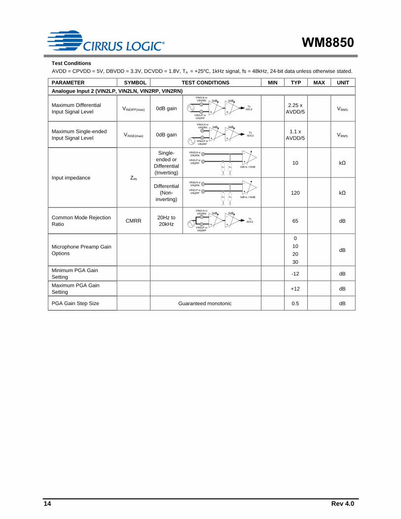
Analogue Input 2 (VIN2LP, VIN2LN, VIN2RP, VIN2RN)
Maximum Differential
Input Signal Level VINDIFF(max) 0dB gain
-
+
0dBVIN2LN or
VIN2RN
VIN2LP or
VIN2RP
To
ADC2
-
+
0dB
2.25 x
AVDD/5 VRMS
Maximum Single-ended
Input Signal Level VINSE(max) 0dB gain
-
+
0dBVIN2LN or
VIN2RN
VIN2LP or
VIN2RP
To
ADC2
-
+
0dB
1.1 x
AVDD/5 VRMS
Input impedance ZIN
Single-
ended or
Differential
(Inverting)
-
+
VIN2LN or
VIN2RN
VIN2LP or
VIN2RP
ZIN ZIN 0dB to +30dB
10 kΩ
Differential
(Non-
inverting)
-
+
VIN2LN or
VIN2RN
VIN2LP or
VIN2RP
ZIN ZIN 0dB to +30dB
120 kΩ
Common Mode Rejection
Ratio CMRR
20Hz to
20kHz
-
+
0dBVIN2LN or
VIN2RN
VIN2LP or
VIN2RP
To
ADC2
-
+
0dB
65 dB
Microphone Preamp Gain
Options
0
10
20
30
dB
Minimum PGA Gain
Setting -12 dB
Maximum PGA Gain
Setting +12 dB
PGA Gain Step Size Guaranteed monotonic 0.5 dB
WM8850
Rev 4.0 15
Test Conditions
AVDD = CPVDD = 5V, DBVDD = 3.3V, DCVDD = 1.8V, TA = +25oC, 1kHz signal, fs = 48kHz, 24-bit data unless otherwise stated.
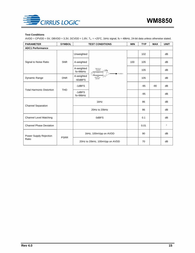
PARAMETER SYMBOL TEST CONDITIONS MIN TYP MAX UNIT
ADC1 Performance
Signal to Noise Ratio SNR
Unweighted
-
+
0dBVIN1LN or
VIN1RN
VIN1LP or
VIN1RP
To ADC1
102 dB
A-weighted 100 105 dB
A-weighted
fs=96kHz 105 dB
Dynamic Range DNR A-weighted
-60dBFS 105 dB
Total Harmonic Distortion THD
-1dBFS -95 -90 dB
-1dBFS
fs=96kHz -95 dB
Channel Separation
1kHz 86 dB
20Hz to 20kHz 86 dB
Channel Level Matching 0dBFS 0.1 dB
Channel Phase Deviation 0.01 °
Power Supply Rejection
Ratio PSRR
1kHz, 100mVpp on AVDD 90 dB
20Hz to 20kHz, 100mVpp on AVDD 70 dB

WM8850
16 Rev 4.0
Test Conditions
AVDD = CPVDD = 5V, DBVDD = 3.3V, DCVDD = 1.8V, TA = +25oC, 1kHz signal, fs = 48kHz, 24-bit data unless otherwise stated.
PARAMETER SYMBOL TEST CONDITIONS MIN TYP MAX UNIT
ADC2 Performance
Signal to Noise Ratio SNR
Unweighted
-
+
0dBVIN2LN or
VIN2RN
VIN2LP or
VIN2RP
To
ADC2
-
+
0dB
100 dB
A-weighted 95 103 dB
A-weighted
fs=96kHz 103 dB
Dynamic Range DNR A-weighted
-60dBFS 103 dB
Total Harmonic Distortion THD -1dBFS -95 -90 dB
Channel Separation
1kHz 87 dB
20Hz to 20kHz 84 dB
Channel Level Matching 0dBFS 0.1 dB
Channel Phase Deviation 0.01 °
Power Supply Rejection
Ratio PSRR
1kHz, 100mVpp on AVDD 90 dB
20Hz to 20kHz, 100mVpp on AVDD 70 dB
Test Conditions
AVDD = CPVDD = 5V, DBVDD = 3.3V, DCVDD = 1.8V, TA = +25oC, 1kHz signal, fs = 48kHz, 24-bit data unless otherwise stated.
PARAMETER SYMBOL TEST CONDITIONS MIN TYP MAX UNIT
Microphone Bias Generator
Output Voltage
VRefEn[2:0] = 001 0.5x
AVDD V
VRefEn[2:0] = 100 0.8x
AVDD V
Current Source Capability 2.5 mA
Power Supply Rejection
Ratio PSRR
1kHz, 100mVpp on AVDD 100 dB
20Hz to 20kHz, 100mVpp on AVDD 88 dB
WM8850
Rev 4.0 17
Test Conditions
AVDD = CPVDD = 5V, DBVDD = 3.3V, DCVDD = 1.8V, TA = +25oC, 1kHz signal, fs = 48kHz, 24-bit data unless otherwise stated.
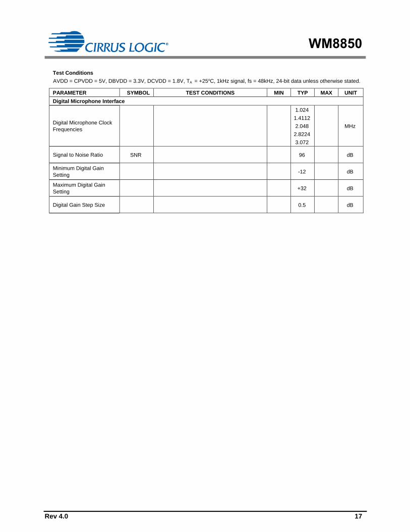
PARAMETER SYMBOL TEST CONDITIONS MIN TYP MAX UNIT
Digital Microphone Interface
Digital Microphone Clock
Frequencies
1.024
1.4112
2.048
2.8224
3.072
MHz
Signal to Noise Ratio SNR 96 dB
Minimum Digital Gain
Setting -12 dB
Maximum Digital Gain
Setting +32 dB
Digital Gain Step Size 0.5 dB

WM8850
18 Rev 4.0
Test Conditions
AVDD = CPVDD = 5V, DBVDD = 3.3V, DCVDD = 1.8V, TA = +25oC, 1kHz signal, fs = 48kHz, 24-bit data unless otherwise stated.
PARAMETER SYMBOL TEST CONDITIONS MIN TYP MAX UNIT
Analogue Output 1 (VOUT1L, VOUT1R)
Full Scale Output Signal
Level VOUT
RL = 1kΩ
to 47kΩ
H-Phn
Enable = 0
-
+
From
DAC1
VOUT1L or
VOUT1R
1kΩ ~
47kΩ
2 x
AVDD/5 VRMS
RL = 16Ω
to 1kΩ
H-Phn
Enable = 1
-
+
From
DAC1
VOUT1L or
VOUT1R
16Ω ~
1kΩ
0.8 x
AVDD/5 VRMS
Maximum Rated Output
Power POUT(max) RL = 16Ω
-
+
From
DAC1
VOUT1L or
VOUT1R
16Ω
40 mW
Load Impedance RL 16 47k Ω
Load Capacitance CL 1 nF
DC Offset Measured between VOUT1L/R and AGND with
path fully enabled but no signal playing -1 0 +1 mV
Analogue Output 2 (VOUT2L, VOUT2LN, VOUT2RP, VOUT2RN)
Differential Full Scale
Output Signal Level VOUT
RL = 5kΩ
to 47kΩ
-
+
From
DAC2
VOUT2LN or
VOUT2RN
VOUT2LP or
VOUT2RP
1pF ~
1nF
5kΩ ~
47kΩ
5kΩ ~
47kΩ
2 x
AVDD/5 VRMS
Single-ended Full Scale
Output Signal Level VOUT
RL = 5kΩ
to 47kΩ
-
+
From
DAC2
VOUT2LP or
VOUT2RP
5kΩ ~
47kΩ
1 x
AVDD/5 VRMS
Load Impedance RL 5 47 kΩ
Load Capacitance CL 1 nF
Analogue Output 3 (VOUT3L, VOUT3LN, VOUT3RP, VOUT3RN)
Differential Full Scale
Output Signal Level VOUT
RL = 5kΩ
to 47kΩ
-
+
From
DAC3
VOUT3LN or
VOUT3RN
VOUT3LP or
VOUT3RP
1pF ~
1nF
5kΩ ~
47kΩ
5kΩ ~
47kΩ
2 x
AVDD/5 VRMS
Single-ended Full Scale
Output Signal Level VOUT
RL = 5kΩ
to 47kΩ
-
+
From
DAC3
VOUT3LP or
VOUT3RP
5kΩ ~
47kΩ
1 x
AVDD/5 VRMS
Load Impedance RL 5 47 kΩ
Load Capacitance CL 1 nF

WM8850
Rev 4.0 19
Test Conditions
AVDD = CPVDD = 5V, DBVDD = 3.3V, DCVDD = 1.8V, TA = +25oC, 1kHz signal, fs = 48kHz, 24-bit data unless otherwise stated.
PARAMETER SYMBOL TEST CONDITIONS MIN TYP MAX UNIT
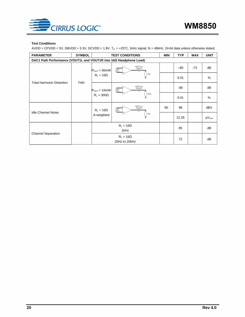
DAC1 Path Performance (VOUT1L and VOUT1R into 10kΩ Line Load)
Signal to Noise Ratio SNR
Unweighted
-
+
From
DAC1
VOUT1L or
VOUT1R
10kΩ
105 dB
A-weighted 100 108 dB
A-weighted
fs=96kHz 108 dB
Out of Band Signal to
Noise Ratio (0.6fs to
150kHz)
OBSNR
Fs >
11.025kHz 80 dB
Fs <=
11.025kHz 75 dB
Dynamic Range DNR A-weighted
-60dBFS 108 dB
Total Harmonic Distortion THD
0dBFS -96 -85 dB
0dBFS
fs=96kHz -96 -85 dB
Channel Separation
1kHz 115 dB
20Hz to 20kHz 110 dB
Channel Level Matching 0dBFS 0.1 dB
Channel Phase Deviation 0.01 °
AVDD Power Supply
Rejection Ratio
AVDD
PSRR
1kHz, 100mVpp on AVDD 51 dB
20Hz to 20kHz, 100mVpp on AVDD 50 dB
CPVDD Power Supply
Rejection Ratio
CPVDD
PSRR
1kHz, 100mVpp on CPVDD 86 dB
20Hz to 20kHz, 100mVpp on CPVDD 75 dB
WM8850
20 Rev 4.0
Test Conditions
AVDD = CPVDD = 5V, DBVDD = 3.3V, DCVDD = 1.8V, TA = +25oC, 1kHz signal, fs = 48kHz, 24-bit data unless otherwise stated.
PARAMETER SYMBOL TEST CONDITIONS MIN TYP MAX UNIT
DAC1 Path Performance (VOUT1L and VOUT1R into 16Ω Headphone Load)
Total Harmonic Distortion THD
POUT = 30mW
RL = 16Ω
-
+
From
DAC1
VOUT1L or
VOUT1R
16Ω
--80 -73 dB
0.01 %
POUT = 10mW
RL = 300Ω
-
+
From
DAC1
VOUT1L or
VOUT1R
300Ω
-80 dB
0.01 %
Idle Channel Noise RL = 16Ω
A-weighted
-
+
From
DAC1
VOUT1L or
VOUT1R
16Ω
90 98 dBV
12.26 μVrms
Channel Separation
RL = 16Ω
1kHz 85 dB
RL = 16Ω
20Hz to 20kHz 72 dB
WM8850
Rev 4.0 21
Test Conditions
AVDD = CPVDD = 5V, DBVDD = 3.3V, DCVDD = 1.8V, TA = +25oC, 1kHz signal, fs = 48kHz, 24-bit data unless otherwise stated.
PARAMETER SYMBOL TEST CONDITIONS MIN TYP MAX UNIT
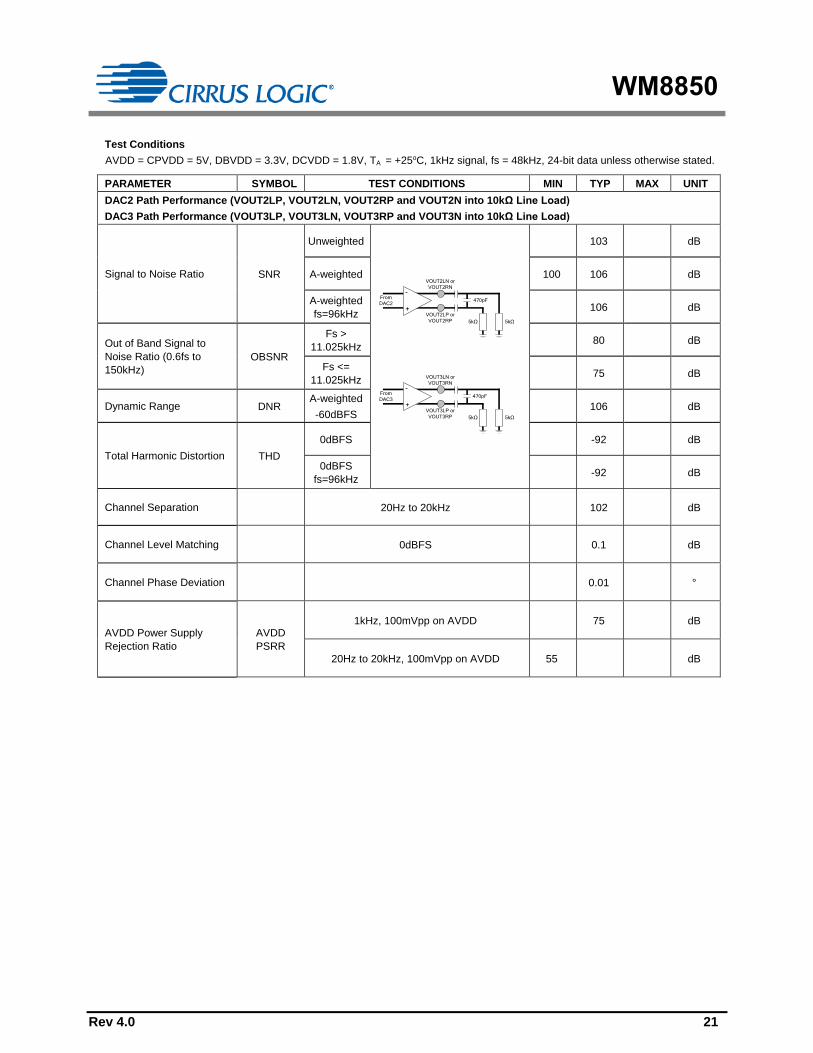
DAC2 Path Performance (VOUT2LP, VOUT2LN, VOUT2RP and VOUT2N into 10kΩ Line Load)
DAC3 Path Performance (VOUT3LP, VOUT3LN, VOUT3RP and VOUT3N into 10kΩ Line Load)
Signal to Noise Ratio SNR
Unweighted
-
+
From
DAC2
VOUT2LN or
VOUT2RN
VOUT2LP or
VOUT2RP
470pF
5kΩ 5kΩ
-
+
From
DAC3
VOUT3LN or
VOUT3RN
VOUT3LP or
VOUT3RP
470pF
5kΩ 5kΩ
103 dB
A-weighted 100 106 dB
A-weighted
fs=96kHz 106 dB
Out of Band Signal to
Noise Ratio (0.6fs to
150kHz)
OBSNR
Fs >
11.025kHz 80 dB
Fs <=
11.025kHz 75 dB
Dynamic Range DNR A-weighted
-60dBFS 106 dB
Total Harmonic Distortion THD
0dBFS -92 dB
0dBFS
fs=96kHz -92 dB
Channel Separation 20Hz to 20kHz 102 dB
Channel Level Matching 0dBFS 0.1 dB
Channel Phase Deviation 0.01 °
AVDD Power Supply
Rejection Ratio
AVDD
PSRR
1kHz, 100mVpp on AVDD 75 dB
20Hz to 20kHz, 100mVpp on AVDD 55 dB
WM8850
22 Rev 4.0
Test Conditions
AVDD = CPVDD = 5V, DBVDD = 3.3V, DCVDD = 1.8V, TA = +25oC, 1kHz signal, fs = 48kHz, 24-bit data unless otherwise stated.
PARAMETER SYMBOL TEST CONDITIONS MIN TYP MAX UNIT
S/PDIF Receiver Specification
Input Signal Level IEC-60958 Compatible Input Mode 200 500 mVp-p
Input Signal Logic High VIH(S/PDIF)
Normal CMOS Compatible Input Mode 0.7 *
DBVDD V
Low-Amplitude CMOS Compatible Input Mode 0.4 *
DBVDD 1.8 V
Input Signal Logic Low VIL(S/PDIF)
Normal CMOS Compatible Input Mode 0.3 *
DBVDD V
Low-Amplitude CMOS Compatible Input Mode DBVDD
x 0.2 V
Input Pin Bias Voltage IEC-60958 Compatible Input Mode 0.5 *
DCVDD V
Input Impedance ZIN
IEC-60958 Compatible Input Mode 7.5 kΩ
Normal CMOS Compatible Input Mode 100 kΩ
Input Hysteresis IEC-60958 Compatible Input Mode 50 mV
Normal CMOS Compatible Input Mode 300 mV
Low-Amplitude CMOS Compatible Input Mode 150 mV
Input Sample Rate Lock
Tolerance
Includes maximum reference clock error of
±0.025% as allowed by HDA Specification
10000 ppm
-1 +1 %
Lock Delay 3
192
Frame
Blocks
S/PDIF Stream Jitter
Tolerance UI = 1/fs(in) 10 UI
Input Sample Rate
Support
32
44.1
48
88.2
96
kHz

WM8850
Rev 4.0 23
Test Conditions
AVDD = CPVDD = 5V, DBVDD = 3.3V, DCVDD = 1.8V, TA = +25oC, 1kHz signal, fs = 48kHz, 24-bit data unless otherwise stated.
PARAMETER SYMBOL TEST CONDITIONS MIN TYP MAX UNIT
S/PDIF Transmitter Specification
Output Signal Logic High VOH(S/PDIF) 0.9 *
DBVDD V
Output Signal Logic Low VOL(S/PDIF) 0.1 *
DBVDD V
Output Current
Source/Sink Capability
DBVDD = 1.8V 7 mA
DBVDD = 3.63V 15 mA
Output Sample Rate
Tolerance
Includes maximum reference clock error of
±0.025% as allowed by HDA Specification
1000 ppm
-0.1 +0.1 %
Output Sample Rate
Support
32
44.1
48
88.2
96
176.4
192
kHz
WM8850
24 Rev 4.0
Test Conditions
AVDD = CPVDD = 5V, DBVDD = 3.3V, DCVDD = 1.8V, TA = +25oC, 1kHz signal, fs = 48kHz, 24-bit data unless otherwise stated.
PARAMETER SYMBOL TEST CONDITIONS MIN TYP MAX UNIT
Analogue References
Positive Voltage
Reference VREFP
0.9 *
AVDD V
Negative Voltage
Reference VREFN
0.1 *
AVDD V
Midrail Voltage Reference VMID 0.5 *
AVDD V
Charge Pump Cap Level CPCAP 3.15 V
Midrail Voltage
Resistance RVMID
AVDD to VMID or VMID to AGND
VMID_SEL[1:0]=00 12.5 kΩ
AVDD to VMID or VMID to AGND
VMID_SEL[1:0]=01 75 kΩ
AVDD to VMID or VMID to AGND
VMID_SEL[1:0]=10 37.5 kΩ
AVDD to VMID or VMID to AGND
VMID_SEL[1:0]=11 375 kΩ
Digital Input / Output
Input High Level VIH 0.65 *
DBVDD V
Input Low Level VIL 0.35 *
DBVDD V
Output High Level VOH 0.9 *
DBVDD V
Output Low Level VOL 0.1 *
DBVDD V
Input Capacitance 7.5 pF
Input Leakage -0.1 +0.1 µA

WM8850
Rev 4.0 25
TERMINOLOGY
1. Signal-to-Noise Ratio (dB) – SNR is a measure of the difference in level between the full scale output signal and the
output with no input signal applied.
2. Total Harmonic Distortion (dB) – THD is the level of the rms value of the sum of harmonic distortion products relative
to the amplitude of the applied input signal.
3. Total Harmonic Distortion plus Noise (dB) – THD+N is the level of the rms value of the sum of harmonic distortion
products plus noise in the specified bandwidth relative to the amplitude of the applied input signal.
4. Crosstalk (L/R) (dB) – left-to-right and right-to-left channel crosstalk is the measured signal level in the idle channel at
the test signal frequency relative to the signal level at the output of the active channel. The active channel is
configured and supplied with an appropriate input signal to drive a full scale output, with signal measured at the output
of the associated idle channel. For example, measured signal level on the output of the idle right channel with a full
scale signal level at the output of the active left channel.
5. Multi-Path Channel Separation (dB) – is the measured signal level in the idle path at the test signal frequency relative
to the signal level at the output of the active path. The active path is configured and supplied with an appropriate input
signal to drive a full scale output, with signal measured at the output of the specified idle path.
6. All performance measurements carried out with 20kHz low pass filter, and where noted an A-weighted filter. Failure to
use such a filter will result in higher THD and lower SNR readings than are found in the Electrical Characteristics. The
low pass filter removes out of band noise; although it is not audible it may affect dynamic specification values.
7. Mute Attenuation – This is a measure of the difference in level between the full scale output signal and the output with
mute applied.
8. Channel Level Matching (dB) – the difference in output level between channels in a stereo pair.
9. Channel Phase Deviation (Degrees) – the difference in phase between channels in a stereo pair.
10. Idle Channel Noise (dBV) – absolute rms measurement of the noise floor over the 20Hz to 20kHz band.

WM8850
26 Rev 4.0
POWER CONSUMPTION
Test Conditions
AVDD = CPVDD = 5V, DCVDD = DBVDD = 1.8V, TA = +25oC, fs = 48kHz, 24-bit data unless otherwise stated.
PARAMETER TEST CONDITIONS AVDD
(mA)
CPVDD
(mA)
DBVDD
(mA)
DCVDD
(mA)
Render paths
Headphone playback only DAC1 & AFG D0, stream enabled
RL=47kΩ, quiescent 26.1 8.1 <0.1 9.1
Headphone playback & one
line output
DAC1, DAC2 & AFG D0, stream enabled
RL=47kΩ, quiescent 36.7 8.1 <0.1 10.2
Stereo line output only DAC2 or DAC3 & AFG D0, stream enabled
RL=47kΩ, quiescent 23.3 0.0 <0.1 9.0
All analogue outputs
DAC1, DAC2, DAC3 & AFG D0, stream
enabled
RL=47kΩ, quiescent
47.0 8.0 <0.1 11.4
Capture paths
Line record only ADC1 & AFG D0, stream enabled
quiescent 46.2 0.0 0.1 9.3
Analogue microphone record
only
ADC1 & AFG D0, stream enabled
quiescent 53.8 0.0 0.1 9.3
Combination paths
Headphone playback &
microphone record
ADC1, DAC1 & AFG D0, stream enabled
quiescent 62.9 8.1 0.1 13.0
All blocks enabled All blocks D0 106.6 8.1 0.1 15.8
All blocks disabled All blocks D3(Note 1), BCLK stopped 12.3 0.0 <0.1 2.4
All blocks disabled, lowest
power mode Vendor-specific D4(Note 2), BCLK stopped 0.0 0.0 0.0 2.4
Notes:
1. D3 state allows for jack detect events to issue wake command to enable the system to wake-up
2. D4 state powers down all analogue circuit blocks. CODEC can no longer generate wakes, but can be woken up using the
HD Link and initialised normally without the need for a power cycle.
WM8850
Rev 4.0 27
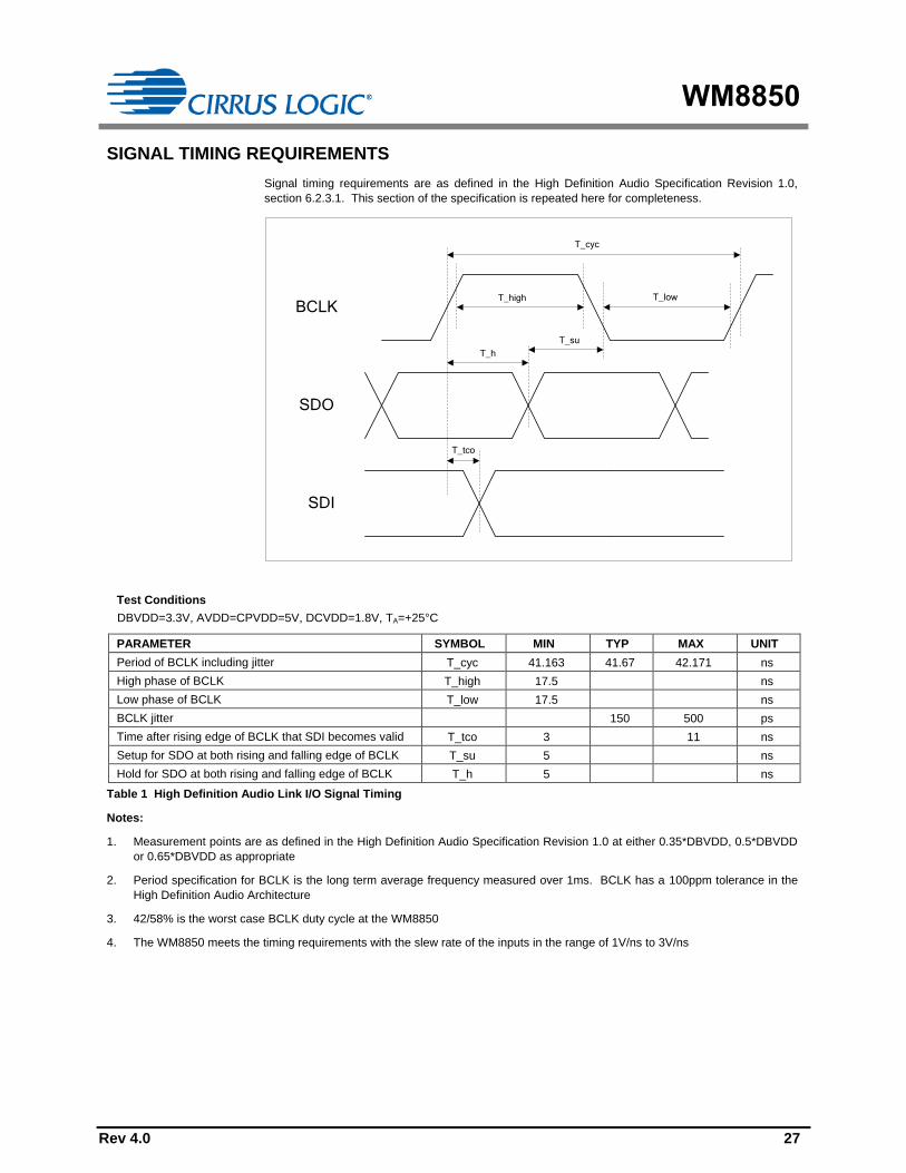
SIGNAL TIMING REQUIREMENTS
Signal timing requirements are as defined in the High Definition Audio Specification Revision 1.0,
section 6.2.3.1. This section of the specification is repeated here for completeness.
BCLK
SDO
SDI
T_cyc
T_high T_low
T_h
T_su
T_tco
Test Conditions
DBVDD=3.3V, AVDD=CPVDD=5V, DCVDD=1.8V, TA=+25°C
PARAMETER SYMBOL MIN TYP MAX UNIT
Period of BCLK including jitter T_cyc 41.163 41.67 42.171 ns
High phase of BCLK T_high 17.5 ns
Low phase of BCLK T_low 17.5 ns
BCLK jitter 150 500 ps
Time after rising edge of BCLK that SDI becomes valid T_tco 3 11 ns
Setup for SDO at both rising and falling edge of BCLK T_su 5 ns
Hold for SDO at both rising and falling edge of BCLK T_h 5 ns
Table 1 High Definition Audio Link I/O Signal Timing
Notes:
1. Measurement points are as defined in the High Definition Audio Specification Revision 1.0 at either 0.35*DBVDD, 0.5*DBVDD
or 0.65*DBVDD as appropriate
2. Period specification for BCLK is the long term average frequency measured over 1ms. BCLK has a 100ppm tolerance in the
High Definition Audio Architecture
3. 42/58% is the worst case BCLK duty cycle at the WM8850
4. The WM8850 meets the timing requirements with the slew rate of the inputs in the range of 1V/ns to 3V/ns

WM8850
28 Rev 4.0
INTERNAL POWER ON RESET CIRCUIT
Power On Reset
Circuit
DCVDD
RESET
VDD
GND
AGND
T(Internal Signal)
Figure 2 Internal Power on Reset Circuit Schematic
The WM8850 includes an internal Power-On-Reset Circuit, as shown in Figure 2, which is used to
reset the digital logic into a default state after power up. The POR circuit is both powered from and
monitors DCVDD. It asserts the internal RESET¯¯¯¯¯¯ low if DCVDD is below a minimum threshold.
DCVDD
Vpor_on
AGND
Internal
POR active
LO
HI
Device ReadyInternal
POR activeNo Power
POR
Undefined
Vpor_off
Vpor_active
RESET
Figure 3 Typical Power up Sequence
Figure 3 shows a typical power-up sequence. The RESET¯¯¯¯¯¯ signal is undefined until DCVDD has
exceeded the minimum threshold, Vpor_active. Once this threshold has been exceeded, RESET¯¯¯¯¯¯ is
asserted low and the chip is held in reset. In this condition, all stimulus to the WM8850 is ignored.
Once DCVDD has reached Vpor_on, RESET¯¯¯¯¯¯ is released high, all registers are in their default state and
access to the WM8850 via the HDA Interface may take place.
On power down, RESET¯¯¯¯¯¯ is asserted low whenever DCVDD drops below the minimum threshold
Vpor_off.
Typical Power-On Reset parameters for the WM8850 are defined in Table 2.
SYMBOL MIN TYP MAX UNIT
Vpor_active 0.1 V
Vpor_on 1.23 V
Vpor_off 1.16 V
Table 2 Typical Power-On Reset parameters

WM8850
Rev 4.0 29
INTRODUCTION
The WM8850 is a high performance multi-channel audio CODEC designed for high performance PC
audio systems. The device offers full compatibility with the Intel High Definition Audio (HDA)
specification revision 1.0, allowing seamless integration with industry-standard HDA controllers.
The WM8850 has three high performance stereo DACs to enable six channels of high definition
audio, ideal for 5.1 channel applications. A high-performance ground-referenced stereo headphone
amplifier utilises advanced charge pump and DC servo technology to minimise system cost and
space without compromise on audio quality. Two stereo pairs of line outputs are also provided.
These line outputs may be used at the output of the PC to enable connection to a 5.1 speaker
system, or may be used connected to external speaker drivers in a notebook or netbook application.
The WM8850 also has two high performance stereo ADCs to provide Hi-Fi quality analogue line-in
and microphone input digitisation. A low noise microphone bias with programmable output voltage is
provided, ideally suited as a bias current source for ECM microphones. Additionally, the CODEC
contains a digital microphone interface capable of supporting up to four independent digital
microphones, allowing high quality microphone array implementations to be realised. One differential
stereo input is provided for line level signals, while one pseudo-differential stereo input with integrated
microphone preamplifier is provided.
The WM8850 also contains a S/PDIF transceiver which is fully compatible with IEC-60958-3. The
S/PDIF receive and transmit paths each contain a sample rate converter (SRC) to enable
asynchronous sample rate conversion between the S/PDIF receive/transmit and HDA interface clock
domains. An additional S/PDIF transmitter is provided to allow direct output of a stereo stream from
the HDA interface.
The WM8850 includes an integrated beep generator allowing system beeps to be played back
through the output paths.
This datasheet assumes familiarity with the High Definition Audio Specification Revision 1.0, available
from http://www.intel.com/standards/hdaudio/. For those verbs implemented in the WM8850 which
are as defined in the High Definition Audio Specification Revision 1.0 there is no detailed text
describing their use in this datasheet. However, detailed text describing the function of of vendor-
specific verbs is provided. Additionally, a full list of each node and each verb implemented in the
WM8850 is provided at the rear of the document.
CIRRUS LOGIC INTERPRETATION OF HDA SPECIFICATION
DOLBY AC3 (IEC-61937)
The AFG node and Converter Widget nodes have a parameter called AC3 within the Supported
Stream Formats Parameter. The Intel High Definition Audio specification states that AC3 should be
set to 1 if the node supports Dolby AC3 (IEC-61937) encoded data.
There is some ambiguity as to what is meant by “supports Dolby AC3 (IEC-61937)”. The WM8850
does not support processing of Dolby AC3 (IEC-61937) encoded data but it does support the passing
of AC3 data through the S/PDIF Converter Widgets.
Cirrus Logic interprets the Intel specification to mean that the AC3 parameter should be set if a node
supports the encoding/decoding of AC3 data, and so we set the WM8850 AC3 parameters to 0.
When the S/PDIF Converters are passing AC3 (IEC-61937) data, the Stream Format Verb for the
widget node should have Bits = 1 (for 16-bit formatting) and Type = 1 to indicate that non-PCM data is
being passed. Note that setting Type is for controller purposes only, and the WM8850 performs the
same operation regardless of what Type is set to.
The user should ensure that Sample Rate Converters (SRCs) are bypassed when S/PDIF contains
AC3 data.
FLOAT32
The WM8850 performs a Fixed-point/Floating-point conversion. Fixed point format is <1,23>, while
floating point format is IEEE-754, single precision 32-bit, full scale between -1.0 and 1.0 with silence
at 0.0.
WM8850
30 Rev 4.0
Floating point conversion is implemented in all Converter widgets. The conversion is enabled when
the Stream Format Verb for the widget node has Bits set to 4 (for 32-bit formatting).
AUDIO WIDGETS CAPABILITIES PARAMETER: DIGITAL
The MIC1 audio path can begin at either Port-B (Analogue Microphone) or Port-D (Digital
Microphone). This leads to some confusion when setting the Widget Capability Parameter. Bit [9] of
this parameter is called Digital and is used to indicate if the widget acts on an analogue stream or on
a digital stream.
In the cases of the MIC1 Converter (NID = 03h) and the MIC1 Mux (NID = 09h), these can act on both
analogue or digital streams, depending on which microphone interface is being used. For these two
nodes, Digital = 0 to indicate that the nodes act on analogue data, but the user should be aware that
these nodes can also act on digital data when the digital microphone is being used.
The Port-D node has its Digital parameter set to 1 to indicate that it acts on digital data.
LATENCY
The group delay or latency for an audio path varies based on sample rate and processing steps (e.g.
SRC). As variable reporting is not supported as part of the Intel HDA Specification, the Delay
parameter in the Audio Widgets Capabilities Parameter is set to 0 to indicate that latency is not
reported.
POWER STATES
Within the AFG, all power states are supported. These are interpreted as follows:
D0: Fully on
D1: Link active, Jack detection logic on, analogue references enabled, but converters and
DSP logic still disabled.
D2: Link active, Jack detection logic on, register read/write access possible but all modules
in an audio path are disabled.
D3: Link disabled (i.e. BCLK stopped), responses not possible but Jack detection logic on
and capable of issuing a wake.
D4: Power applied, and settings maintained. Jack detection logic off, and wake disabled.
The AFG node supports the Power State verb. Widget nodes also offer power control, but their
settings are restricted to select only power states below that of the AFG power state setting. For
example, if the AFG node is set at D1, widget nodes can be set to D1, D2, D3, but not D0.
The default power state of the AFG is D2 so as to allow the PLLs to lock during CODEC initialisation.
The default power state of the widget nodes is D3 so as to minimise power consumption. Widget
nodes do not support D4 as the D3 state is identical to D4 at the widget node level.
Power state transitions are done in sequence. For example, if a node is in power state D3, and the
power state is set to D0, the transitions steps are D3-D2-D1-D0. If a Get Power State command is
issued during the state transitions, the actual power state returned, will be the power state at the end
of the frame that the Power State command was issued in.
It is possible that the actual power state returned is D3, D2 or D0 while the set power state returned is
D0.
For low power operation, the link should be in the Link Reset state and the WM8850 AFG should be
in D3 or D4. If the link is in the Link Reset state, and the WM8850 AFG was left in states D0, D1 or
D2, the WM8850 cannot issue a power state changes request (i.e. wake).
The only settings that can be changed in the D4 state is the AFG Power State or AFG reset settings –
any other changes will be ignored.

WM8850
Rev 4.0 31
In D3, BCLK may be stopped after the WM8850 asserts the PS-ClkStopOK register in the AFG’s
Power State verb. The PS-ClkStopOK bit will remain asserted in power state D3 until the power state
is modified to D0, D1 or D2. If the power state is changed to D4 while in power state D3 when the
PS-ClkStopOK bit is set, software must poll the AFG PS-Act bits to determine when the WM8850
reports transition to power state D4 complete (and hence reports PS-Act as D4) before stopping the
BCLK.
In D3, if the link is not in the Link Reset state and BCLK is running, the WM8850 will issue an
unsolicited response rather than a wake.
In D3 (with the link is the Link Reset state), the WM8850 is capable of generating a wake (i.e. a power
state change request). The Controller will respond to the wake by putting the WM8850 through an
initialisation sequence. The initialisation sequence will not change the register settings, so the
WM8850 will still report a power state of D3 but the WM8850 will be able to send responses, including
any unsolicited response(s) that caused a wake to be issued.
As register settings are maintained in the D3/D4 states, the user should be aware that if the WM8850
is brought from D3/D4 to D0 and stream IDs had been previously assigned, data rendering and
capture will commence. If this behaviour is not desired, the user should bring the WM8850 to state
D3 and set the stream IDs to 0, or ensure that stream IDs are set to 0 prior to entering the D3/D4
state.
STREAM START/STOP
Sections 4.5.3 and 4.5.4 of the Intel HD Audio specification describe the starting and stopping of
streams. While the descriptions are sufficient from a controller perspective, there are ambiguities from
a CODEC perspective.
For each stream that goes through the HDA Link, there is a ‘Stream Manager’ module within the
WM8850 whose function is to assemble/disassemble the stream packets within the link frame. The
Stream Manager is disabled while the Stream value in the Converter Stream, Channel Verb is set to
0h. When disabled, the captured data will not be sent on the link, and data from the link will not be
decoded for rendering.
For audio path configuration, it is assumed that the Stream ID is the last register to be set in the
configuration sequence. When Stream ID is set to a non-zero value it has the effect of starting the
stream. On starting the stream, Stream Managers associated with input converters begin transmitting
data on the link, and Stream Managers associated with output converters begin to decode data with
the corresponding stream tag.
Note: Audio paths with mute capabilities may have ‘un-mute’ as the final configuration step. For
these paths, the stream will have started but the audio data will be zeroed until mute has been
disabled.
There are test paths within the WM8850 that do not use the HDA Link. These paths can still be used
when the Stream Manager is disabled.
The Stream Manager is also disabled when the associated converter widget is in power state D1, D2
or D3. Digital converters (i.e. S/PDIF) have a DigEn register bit. When this is set to 0, the associated
stream manager is disabled.
It is assumed that the settings of the Stream Format Verb and Converter Stream, Channel Verb will
not change when a stream is active (with the exception of changing the Stream ID to 0 to terminate
the stream). Changing stream settings while a stream is active is an erroneous action, and may
result in audio corruption.
SDI STREAM ORDER
The order of stream transmission on the SDI link is governed by the CODEC. The WM8850 will
transmit streams with the lowest stream ID value first.
If a stream is started with a stream ID lower than an existing stream, then the new stream is
transmitted earlier in the frame than the existing stream (i.e. the WM8850 auto-shuffles the stream
placement within the frame). This moves the existing stream to further on in the frame than it was
prior to the starting of the new stream. It is assumed that moving streams within a frame is
acceptable to the Controller.

WM8850
32 Rev 4.0
BANDWIDTH CONFLICTS
Sections 5.3.2.2 and 5.3.3.3 of the HD Audio spec describe the scenario of over-subscription of SDO
and SDI bandwidths. It indicates that the final stream on the link is terminated prior to completion, and
further behaviour is undefined.
SDO
It is possible that the SDO line could be oversubscribed, if all streams are active at their maximum
sample rate, and word length. It is the responsibility of the Controller to handle this situation, and
determine what is put on the SDO line during oversubscription. The WM8850 will produce unsolicited
responses from the converter nodes that have not received the stream packets that they have been
configured for.
SDI
The WM8850 invokes a protection mechanism, should a bandwidth over-subscription situation arise.
The mechanism monitors the sample rate, and sample-size settings of a stream to detect
oversubscription.
If the SDI line is over-subscribed, due to software configuration or configuration from the recovered
S/PDIF sample-rate, the stream (or streams) assigned the highest Stream ID tag value, will be
dropped, and an unsolicited response issued from the stream converter whose stream has been
dropped.
A stream will be restarted on a re-issue of a non-zero stream ID. However, should the bandwidth
problem still be present, the stream won’t start and an unsolicited response will be re-sent.
Although there is a protection mechanism in the WM8850, it is the responsibility of the user to identify
and rectify bandwidth problems.
SOFTWARE FORMATTED (RAW) S/PDIF
An S/PDIF sub-frame consists of a preamble, 24-bits of audio data, and four control bits. In Software
Formatted (Raw) S/PDIF mode, all 24-bits of the audio data, plus the 4 bits of control information,
plus a 4-bit encoding of the preamble (taking the last 4-bits of the 8-bit bi-phase encoded preamble)
are transported across the link. Software Formatted S/PDIF mode is selected by setting the Bits
register in the Stream Format Verb to 4h (i.e. 32-bits) and setting the Type register to 1.
SOURCE SYNCHRONOUS INPUT - S/PDIF RX
Extra Bandwidth
Section 5.4.3 of the HDA specification describes how source synchronous inputs should be handled.
Note: Source synchronous handling is only required when SRC1 is bypassed.
When the incoming sampling rate is slightly higher that the nominal stream sampling rate extra data
transmission is required. The HDA specification states “the CODEC may insert one or more
additional complete sample blocks on the link, either within its normal allocated stream packet
(making it larger than the nominal allocated size) or by creating a second stream packet within the
frame.”
The WM8850 implements the first option, and will insert additional samples (in left/right pairs) within
the stream packet. The Data Length field within the Stream tag will be updated to show that the
stream packet contains additional samples.
If additional samples cannot be accommodated on SDI due to bandwidth problems, the additional
samples are dropped, and an unsolicited response is issued from the S/PDIF Rx Converter Node with
EF_STREAM_DROP set to 01h.
WM8850
Rev 4.0 33
Loss of Lock
Should the S/PDIF Rx lose lock, an unsolicited response will be triggered to indicate the change in
lock status. The data in the link sample blocks will be set to 0, and the stream will continue to run at
the previously recovered sample rate. There may be several samples of data before the unsolicited
response can be sent, but the data will be zeroed immediately.
If the S/PDIF Rx is in Software Formatted S/PDIF mode, and the loss of lock event occurs, all 32-bits
of the data are zeroed.
Change in Sample Rate
Once a stream has started, stream parameters such as sample-size, number of channels, and
sample rates should not be changed. For the S/PDIF Rx audio path, it is expected that any change of
S/PDIF sample rate will cause the S/PDIF Rx to lose lock.
Once the S/PDIF Rx has gained lock to the new sample rate (or regained lock at the existing sample
rate), the controller will be sent an unsolicited response.
The S/PDIF Rx audio path has two methods of handling the relock condition:
1. Push Method: where upon lock, the stream (assuming SRC1 is bypassed) immediately
changes sample rate to the new recovered rate, and data is no longer overwritten with
zeros.
2. Controlled Method: where zeroed data continues to be transmitted at the old sample rate,
until the stream ID is set to 0. Upon re-assignment of the Stream ID, non-zeroed stream
data is transmitted at the newly recovered sample rate.
These methods are selected using the Unlock Ctrl register in the SPDIF_IN Control Verb.
S/PDIF TX VALIDITY FLAG
The validity flag is bit [28] of an S/PDIF sub-frame. It is configured using V-bit in the Digital Converter
Control Verb.
When the V-bit is set to 1, the validity flag for both sub-frames is set to 1.
When the V-bit is set to 0, the validity flag for both sub-frames is set to 0, unless an invalid sample is
being transmitted for that sub-frame - in which case the validity flag is set to 1 for that sub-frame.
An invalid sample may occur under the following conditions:
The Stream ID is set to 0
SRC2 is enabled but is unlocked
There has been a FIFO overrun/under-run condition in the S/PDIF Tx Stream Manager (i.e.
a Stream Error).
Note: A Stream Error problem would only be present due to a problem upstream of the WM8850. A
Stream Error triggers an unsolicited response with the EF_STREAM_ERR flag set. If an invalid
sample is detected, it will be overwritten with all-zeros if VCFG in the Digital Converter Control Verb is
set to 1.
CHANNEL NUMBERING
Multi-Channel Streams
Channels 0, 2, 4, etc will be assigned to the Left Channel of a stereo converter. Channels 1, 3, 5, etc
will be assigned to the Right Channel of a stereo converter.
Channel synchronisation between channels is only guaranteed where stream packets are received by
the WM8850 after all converters in a multi-channel stream have had their stream ID assigned.
WM8850
34 Rev 4.0
Mono Streams
All converters are stereo. Where an input converter (ADC, S/PDIF Rx) is associated with a mono
stream, only the left channel (channel 0) will be sent on the HDA Link.
In mono mode, right channel modules in the ADC will be disabled to save power.
Where an output converter (DAC, S/PDIF Tx) is associated with a mono stream, both left and right
channels render the same samples. If both left and right DAC outputs are not desired, the unwanted
channel can be muted.
A stream is assumed to be mono when its Chan control in the Stream Format Verb is set to 0. The
Channel control in the Converter Stream, Channel Verb should be set to 0, although any setting of
this register gives the same behaviour in mono mode.
ILLEGAL REGISTER VALUES
Should the user set verb registers to illegal, unsupported or reserved values, WM8850 behaviour is
undefined.
Writing to Reserved registers has no effect.
RESPONSE FIELD
Valid Bit
Bit [35] of the Response Field is defined as the Valid Bit. Section 7.3.1 of the HDA specification
states: “A 1 in the Valid bit position indicates the Response Filed contains a valid response, which the
controller will place in the RIRB; a 0 indicates there is no response.”
The WM8850 will set the Valid Bit for all responses, except null responses.
We define a null response as a response to a command that contains an invalid verb (a command
where NID=0h, and Verb=0h), or a response to a command with a CODEC address (CAd) that does
not match the WM8850 CAd. Either of these commands can be considered as a null command.
We define a non-defined command as a command that has no meaning (i.e. a NID that is not within
the WM8850, or a Verb ID that is not supported for the given node). The WM8850 will set the Valid
Bit for non-defined commands.
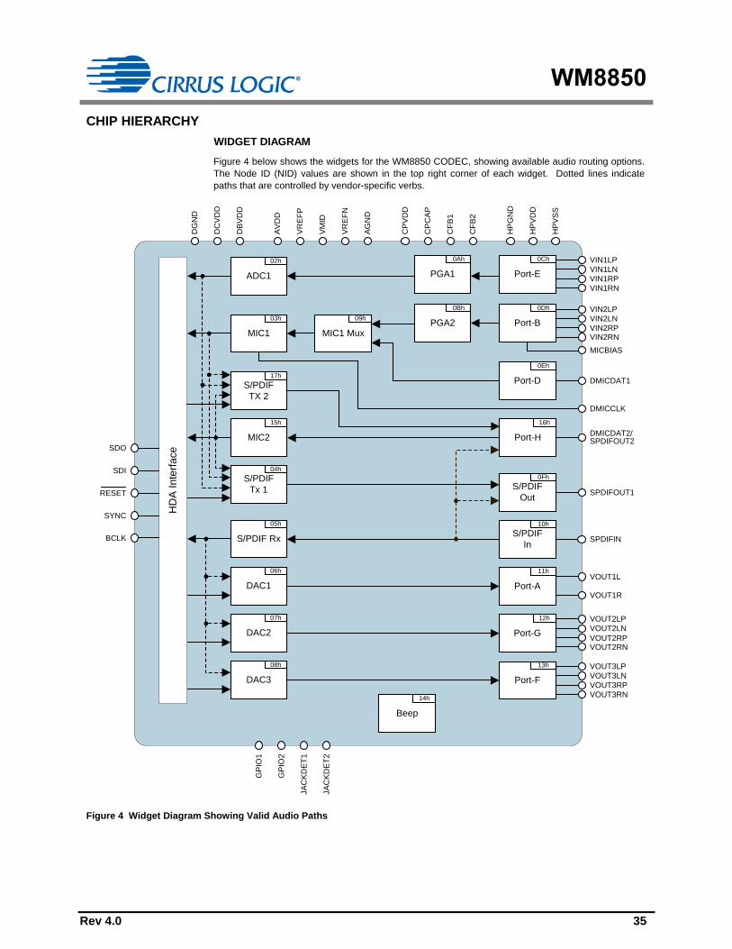
WM8850
Rev 4.0 35
CHIP HIERARCHY
WIDGET DIAGRAM
Figure 4 below shows the widgets for the WM8850 CODEC, showing available audio routing options.
The Node ID (NID) values are shown in the top right corner of each widget. Dotted lines indicate
paths that are controlled by vendor-specific verbs.
HD
A In
terf
ace
Port-E
0Ch
PGA1
0Ah
ADC1
02h
Port-B
0Dh
PGA2
0Bh
MIC1
03h
MIC1 Mux
09h
Port-D
0Eh
S/PDIF
Out
0Fh
S/PDIF
In
10h
Port-A
11h
Port-G
12h
Port-F
13h
S/PDIF
Tx 1
04h
S/PDIF Rx
05h
DAC1
06h
DAC2
07h
DAC3
08h
Port-HMIC2
15h 16h
Beep
14h
S/PDIF
TX 2
17h
VIN2LP
VIN2LN
VIN2RPVIN2RN
MICBIAS
VIN1LP
VIN1LN
VIN1RP
VIN1RN
DMICDAT1
DMICCLK
DMICDAT2/SPDIFOUT2
VOUT1L
VOUT1R
VOUT2LP
VOUT2LN
VOUT2RPVOUT2RN
VOUT3LP
VOUT3LN
VOUT3RP
VOUT3RN
SPDIFIN
SPDIFOUT1
AV
DD
VM
ID
AG
ND
CP
VD
D
CP
CA
P
CF
B1
CF
B2
HP
GN
D
HP
VD
D
DG
ND
DC
VD
D
DB
VD
D
VR
EF
N
VR
EF
P
HP
VS
S
GP
IO1
GP
IO2
JA
CK
DE
T1
JA
CK
DE
T2
SDO
SDI
RESET
SYNC
BCLK
Figure 4 Widget Diagram Showing Valid Audio Paths
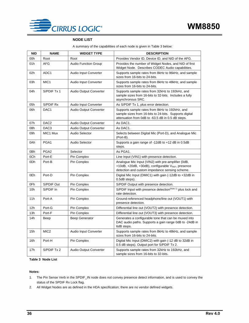
WM8850
36 Rev 4.0
NODE LIST
A summary of the capabilities of each node is given in Table 3 below:
NID NAME WIDGET TYPE DESCRIPTION
00h Root Root Provides Vendor ID, Device ID, and NID of the AFG.
01h AFG Audio Function Group Provides the number of Widget Nodes, and NID of first
Widget Node. Describes CODEC Audio capabilities.
02h ADC1 Audio Input Converter Supports sample rates from 8kHz to 96kHz, and sample
sizes from 16-bits to 24-bits.
03h MIC1 Audio Input Converter Supports sample rates from 8kHz to 48kHz, and sample
sizes from 16-bits to 24-bits.
04h S/PDIF Tx 1 Audio Output Converter Supports sample rates from 32kHz to 192kHz, and
sample sizes from 16-bits to 32-bits. Includes a fully
asynchronous SRC.
05h S/PDIF Rx Audio Input Converter As S/PDIF Tx 1, plus error detection.
06h DAC1 Audio Output Converter Supports sample rates from 8kHz to 192kHz, and
sample sizes from 16-bits to 24-bits. Supports digital
attenuation from 0dB to -63.5 dB in 0.5 dB steps.
07h DAC2 Audio Output Converter As DAC1.
08h DAC3 Audio Output Converter As DAC1.
09h MIC1 Mux Audio Selector Selects between Digital Mic (Port-D), and Analogue Mic
(Port-B).
0Ah PGA1 Audio Selector Supports a gain range of -12dB to +12 dB in 0.5dB
steps.
0Bh PGA2 Selector As PGA1.
0Ch Port-E Pin Complex Line Input (VIN1) with presence detection.
0Dh Port-B Pin Complex Analogue Mic Input (VIN2) with pre-amplifier (0dB,
+10dB, +20dB, +30dB), configurable VREF, presence
detection and custom impedance sensing scheme.
0Eh Port-D Pin Complex Digital Mic Input (DMIC1) with gain (-12dB to +32dB in
0.5dB steps).
0Fh S/PDIF Out Pin Complex S/PDIF Output with presence detection.
10h S/PDIF In Pin Complex S/PDIF Input with presence detection(Note 1) plus lock and
rate detection.
11h Port-A Pin Complex Ground-referenced headphone/line out (VOUT1) with
presence detection.
12h Port-G Pin Complex Differential line out (VOUT2) with presence detection.
13h Port-F Pin Complex Differential line out (VOUT3) with presence detection.
14h Beep Beep Generator Generates a configurable tone that can be muxed into
DAC audio paths. Supports a gain range 0dB to -24dB in
6dB steps.
15h MIC2 Audio Input Converter Supports sample rates from 8kHz to 48kHz, and sample
sizes from 16-bits to 24-bits.
16h Port-H Pin Complex Digital Mic Input (DMIC2) with gain (-12 dB to 32dB in
0.5 dB steps). Output port for S/PDIF Tx 2.
17h S/PDIF Tx 2 Audio Output Converter Supports sample rates from 32kHz to 192kHz, and
sample sizes from 16-bits to 32-bits.
Table 3 Node List
Notes:
1. The Pin Sense Verb in the SPDIF_IN node does not convey presence detect information, and is used to convey the
status of the SPDIF Rx Lock flag.
2. All Widget Nodes are as defined in the HDA specification; there are no vendor defined widgets.
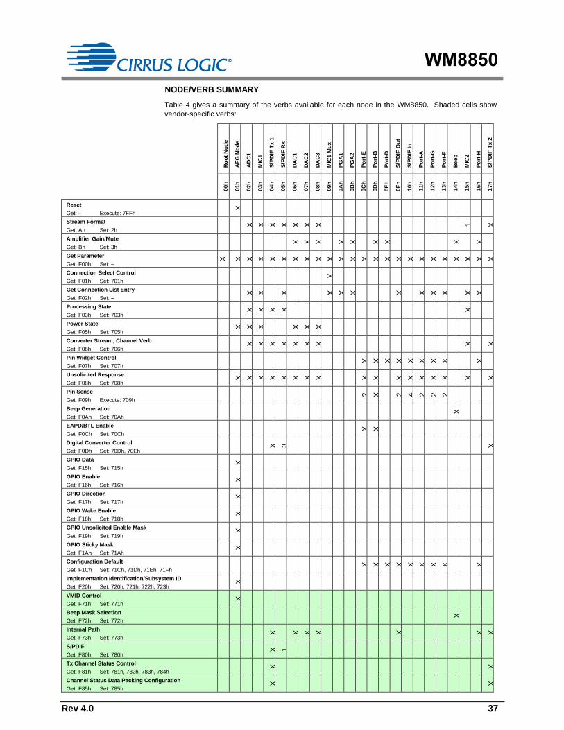
WM8850
Rev 4.0 37
NODE/VERB SUMMARY
Table 4 gives a summary of the verbs available for each node in the WM8850. Shaded cells show
vendor-specific verbs:
Ro
ot
No
de
AF
G N
od
e
AD
C1
MIC
1
S/P
DIF
Tx 1
S/P
DIF
Rx
DA
C1
DA
C2
DA
C3
MIC
1 M
ux
PG
A1
PG
A2
Po
rt-E
Po
rt-B
Po
rt-D
S/P
DIF
Ou
t
S/P
DIF
In
Po
rt-A
Po
rt-G
Po
rt-F
Beep
MIC
2
Po
rt-H
S/P
DIF
Tx 2
00h
01h
02h
03h
04h
05h
06h
07h
08h
09h
0A
h
0B
h
0C
h
0D
h
0E
h
0F
h
10h
11h
12h
13h
14h
15h
16h
17h
Reset
Get: – Execute: 7FFh
X
Stream Format
Get: Ah Set: 2h X
X
X
X
X
X
X 1 X
Amplifier Gain/Mute
Get: Bh Set: 3h
X
X
X X
X X
X X X
Get Parameter
Get: F00h Set: –
X
X
X
X
X
X
X
X
X
X
X
X
X
X
X
X
X
X
X
X
X
X
X
X
Connection Select Control
Get: F01h Set: 701h
X
Get Connection List Entry
Get: F02h Set: –
X
X X X
X
X X X
X
X X
X
Processing State
Get: F03h Set: 703h
X
X
X
X X
Power State
Get: F05h Set: 705h
X
X
X X
X
X
Converter Stream, Channel Verb
Get: F06h Set: 706h
X
X
X
X
X
X
X X X
Pin Widget Control
Get: F07h Set: 707h
X
X
X
X
X
X
X
X X
Unsolicited Response
Get: F08h Set: 708h
X
X
X
X
X
X
X
X X
X X
X
X
X
X X X
Pin Sense
Get: F09h Execute: 709h
2
X 2
4
2
2
2
Beep Generation
Get: F0Ah Set: 70Ah
X
EAPD/BTL Enable
Get: F0Ch Set: 70Ch
X
X
Digital Converter Control
Get: F0Dh Set: 70Dh, 70Eh
X
3 X
GPIO Data
Get: F15h Set: 715h
X
GPIO Enable
Get: F16h Set: 716h
X
GPIO Direction
Get: F17h Set: 717h
X
GPIO Wake Enable
Get: F18h Set: 718h
X
GPIO Unsolicited Enable Mask
Get: F19h Set: 719h
X
GPIO Sticky Mask
Get: F1Ah Set: 71Ah
X
Configuration Default
Get: F1Ch Set: 71Ch, 71Dh, 71Eh, 71Fh
X
X
X
X
X
X
X
X X
Implementation Identification/Subsystem ID
Get: F20h Set: 720h, 721h, 722h, 723h
X
VMID Control
Get: F71h Set: 771h
X
Beep Mask Selection
Get: F72h Set: 772h
X
Internal Path
Get: F73h Set: 773h
X X
X
X X X
X
S/PDIF
Get: F80h Set: 780h
X
1
Tx Channel Status Control
Get: F81h Set: 781h, 782h, 783h, 784h
X X
Channel Status Data Packing Configuration
Get: F85h Set: 785h
X X
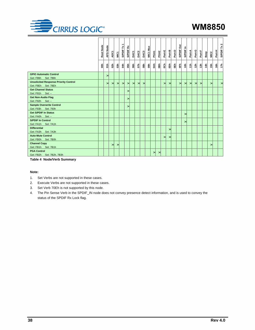
WM8850
38 Rev 4.0
Ro
ot
No
de
AF
G N
od
e
AD
C1
MIC
1
S/P
DIF
Tx 1
S/P
DIF
Rx
DA
C1
DA
C2
DA
C3
MIC
1 M
ux
PG
A1
PG
A2
Po
rt-E
Po
rt-B
Po
rt-D
S/P
DIF
Ou
t
S/P
DIF
In
Po
rt-A
Po
rt-G
Po
rt-F
Beep
MIC
2
Po
rt-H
S/P
DIF
Tx 2
00h
01h
02h
03h
04h
05h
06h
07h
08h
09h
0A
h
0B
h
0C
h
0D
h
0E
h
0F
h
10h
11h
12h
13h
14h
15h
16h
17h
GPIO Automatic Control
Get: F86h Set: 786h
X
Unsolicited Response Priority Control
Get: F8Eh Set: 78Eh
X
X
X
X
X
X
X
X X
X X
X
X
X
X X X
Get Channel Status
Get: F91h Set: –
X
Get Non-Audio Flag
Get: F92h Set: – X
Sample Overwrite Control
Get: F93h Set: 793h
X
Get S/PDIF In Status
Get: FA0h Set: –
X
S/PDIF In Control
Get: FA1h Set: 7A1h
X
Differential
Get: FA3h Set: 7A3h
X
Auto-Mute Control
Get: FB0h Set: 7B0h
X
X
Channel Copy
Get: FB1h Set: 7B1h
X
X X
PGA Control
Get: FB2h Set: 7B2h, 7B3h
X
X
Table 4 Node/Verb Summary
Note:
1. Set Verbs are not supported in these cases.
2. Execute Verbs are not supported in these cases.
3. Set Verb 70Eh is not supported by this node.
4. The Pin Sense Verb in the SPDIF_IN node does not convey presence detect information, and is used to convey the
status of the SPDIF Rx Lock flag.

WM8850
Rev 4.0 39
DEVICE DESCRIPTION
This section of the datasheet provides detailed information on all the major paths through the device,
along with the nodes used and the vendor-specific verbs. For those verbs implemented in the
WM8850 which are as defined in the High Definition Audio Specification Revision 1.0 there is no
detailed text describing their use in this datasheet.
The functions covered in this section of the datasheet, and the WM8850 nodes associated with each,
are listed in Table 5.
FUNCTION NODE NAME NODE ID (NID)
Stereo Analogue Line Record Port-E 0Ch
PGA1 0Ah
ADC1 02h
Stereo Analogue Microphone Record Port-B 0Dh
PGA2 0Bh
MIC1 Mux 09h
MIC1 03h
Digital Microphone Record Port-D 0Eh
MIC1 Mux 09h
MIC1 03h
Port-H 16h
MIC2 15h
Stereo Headphone Playback DAC1 06h
Port-A 11h
Stereo Line Playback DAC2 07h
Port-G 12h
DAC3 08h
Port-F 13h
S/PDIF Receive S/PDIF In 10h
S/PDIF Rx 05h
S/PDIF Transmit S/PDIF Tx 1 04h
S/PDIF Out 0Fh
S/PDIF Tx 2 17h
Port-H 16h
Ancillary Functions
(Beep generator,
VMID control,
GPIO2 automatic control mode,
Unsolicited response priority control)
Beep 14h
AFG 01h
Table 5 WM8850 Device Functions

WM8850
40 Rev 4.0
STEREO ANALOGUE LINE RECORD
Stereo analogue line input is supported using the VIN1LP, VIN1LN, VIN1RP and VIN1RN pins; these
are available for high-quality stereo digitisation through the ADC1 node.
The WM8850 nodes associated with this function are shown in Figure 5.
VIN1LP
VIN1LN
VIN1RP
VIN1RN
ADC1
02h
PGA1
0Ah
Port-E
0Ch
HD
A In
terf
ace
Figure 5 Stereo Analogue Line Record Path
This section provides a summary of the Port-E, PGA1 and ADC1 nodes, and describes the vendor-
specific verb functions associated with each.
PORT-E (NID = 0CH)
Table 6 gives a summary of the Port-E node:
NODE SUMMARY INFORMATION
NID 0Ch
Widget Type Pin Complex
Supported Get Verbs F00h, F07h, F08h, F09h, F0Ch, F1Ch, F8Eh, FB0h
Supported Set Verbs 707h, 708h, 70Ch, 71Ch, 71Dh, 71Eh, 71Fh, 78Eh, 7B0h
Unsolicited Responses Presence Detect Status Change
Vendor-Specific Verbs F8Eh, 78Eh : Unsolicited Response Priority Control Verb
FB0h, 7B0h : Auto-Mute Control Verb
Table 6 Port-E Node Summary Information
Port-E supports two different input configurations, controlled by the EAPD/BTL Verb.
SET VERB BIT BITFIELD
NAME
DEFAULT DESCRIPTION
70Ch 0 BTL 1h Controls the configuration of the input pins on
Port-E:
0 = Single-ended mode
1 = BTL (balanced) mode
In single-ended input mode, VIN1LP and VIN1RP are used as the Port-E input pins VIN1LN and
VIN1RN must be left floating in this mode. Note that the full-scale input signal level is reduced in
single-ended mode, as shown in the “Electrical Characteristics” section.
In differential input mode, VIN1LP, VIN1LN, VIN1RP and VIN1RN are used as the Port-E input pins.
See Figure 6 for examples of the external connections required in each of the supported input
configurations.
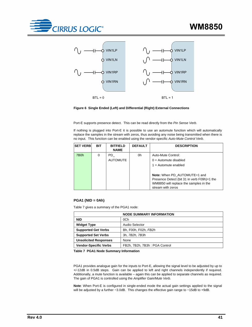
WM8850
Rev 4.0 41
VIN1LP
VIN1RN
VIN1LN
VIN1RP
VIN1LP
VIN1RN
VIN1LN
VIN1RP
BTL = 0 BTL = 1
Figure 6 Single Ended (Left) and Differential (Right) External Connections
Port-E supports presence detect. This can be read directly from the Pin Sense Verb.
If nothing is plugged into Port-E it is possible to use an automute function which will automatically
replace the samples in the stream with zeros, thus avoiding any noise being transmitted when there is
no input. This function can be enabled using the vendor-specific Auto-Mute Control Verb.
SET VERB BIT BITFIELD
NAME
DEFAULT DESCRIPTION
7B0h 0 PD_
AUTOMUTE
0h Auto-Mute Control:
0 = Automute disabled
1 = Automute enabled
Note: When PD_AUTOMUTE=1 and
Presence Detect (bit 31 in verb F09h)=1 the
WM8850 will replace the samples in the
stream with zeros
PGA1 (NID = 0Ah)
Table 7 gives a summary of the PGA1 node:
NODE SUMMARY INFORMATION
NID 0Ch
Widget Type Audio Selector
Supported Get Verbs Bh, F00h, F02h, FB2h
Supported Set Verbs 3h, 7B2h, 7B3h
Unsolicited Responses None
Vendor-Specific Verbs FB2h, 7B2h, 7B3h : PGA Control
Table 7 PGA1 Node Summary Information
PGA1 provides analogue gain for the inputs to Port-E, allowing the signal level to be adjusted by up to
+/-12dB in 0.5dB steps. Gain can be applied to left and right channels independently if required.
Additionally, a mute function is available – again this can be applied to separate channels as required.
The gain of PGA1 is controlled using the Amplifier Gain/Mute Verb.
Note: When Port-E is configured in single-ended mode the actual gain settings applied to the signal
will be adjusted by a further −3.0dB. This changes the effective gain range to −15dB to +9dB.

WM8850
42 Rev 4.0
PGA1 uses an internal zero cross detect circuit to ensure that all gain changes occur while the signal
passes through the zero point. This function eliminates any potential DC steps that can occur if gain
changes are applied at other times, and therefore the potential for zipper noise is removed. If no zero
cross occurs within a specified time after the gain change is requested via a register write a timeout
period will elapse and the gain will be changed regardless. This timeout period can be changed using
the vendor-specific PGA Control Verb:
SET VERB BIT BITFIELD
NAME
DEFAULT DESCRIPTION
7B2h
7B3h
13:0 Terminal
Count
1FFFh Set the period of the zero detect timeout clock:
0000h = Timeout disabled
0001h to 03FFh = Reserved
0400h = 1025 x 20.833µs (21.3ms)
0401h = 1026 x 20.833µs (21.4ms)
…
1FFFh = 8192 × 20.833µs (171ms)
…
3FFFh = 16384 × 20.833µs (341ms)
Note: The timeout clock uses the SYNC signal
from the HDA interface, so the absolute value
of the timeout period will depend on the
absolute accuracy of the SYNC signal.
ADC1 (NID = 02h)
Table 8 gives a summary of the ADC1 node:
NODE SUMMARY INFORMATION
NID 02h
Widget Type Audio Input Converter
Supported Get Verbs Ah, F00h, F02h, F03h, F05h, F06h, F08h, F8Eh, FB1h
Supported Set Verbs 2h, 703h, 705h, 706h, 708h, 78Eh, 7B1h
Unsolicited Responses Stream Drop
Vendor-Specific Verbs F8Eh, 78Eh : Unsolicited Response Priority Control Verb
FB1h, 7B1h : Channel Copy Verb
Table 8 ADC1 Node Summary Information

WM8850
Rev 4.0 43
ADC1 supports all common sample rates from 8kHz to 96kHz and data widths of 16, 20, 24 and 32-
bit (Float-32).
The sample rate and word length of the data captured by the ADC1 node is set using the Stream
Format Verb. Table 9 below shows the required settings for Base, Mult and Div as part of the Stream
Format Verb to obtain the required sample rate.
SAMPLE RATE BASE MULT DIV
8kHz 0h 0h 5h
11.025kHz 1h 0h 3h
16kHz 0h 0h 2h
22.05kHz 1h 0h 1h
24kHz 0h 0h 1h
32kHz 0h 1h 2h
44.1kHz 1h 0h 0h
48kHz 0h 0h 0h
88.2kHz 1h 1h 0h
96kHz 0h 1h 0h
Table 9 ADC1 Supported Sample Rate Settings
Note: Other settings of Base, Mult and Div are reserved and should not be set.
The ADC1 output data is by default set to provide the captured waveform from the left channel in
Channel 0, and the right channel in Channel 1. It is possible to adjust this mapping using the vendor-
specific Channel Copy Verb.
SET VERB BIT BITFIELD
NAME
DEFAULT DESCRIPTION
7B1h 1 CHAN1_
SEL
1 Channel 1 (right) Mapping Control:
0 = Channel 1 takes data from left audio
channel
1 = Channel 1 takes data from right audio
channel
0 CHAN0_
SEL
0 Channel 0 (left) Mapping Control:
0 = Channel 0 takes data from left audio
channel
1 = Channel 0 takes data from right audio
channel

WM8850
44 Rev 4.0
STEREO ANALOGUE MICROPHONE RECORD
Stereo analogue microphone input is supported using the VIN2LP, VIN2LN, VIN2RP and VIN2RN
pins; these are available for analogue microphone digitisation through the MIC1 node. The MICBIAS
output, controlled via the Port-B node, provides a low noise voltage output suitable for use as a power
supply for analogue or digital microphones.
The WM8850 nodes associated with this function are shown in Figure 7.
MICBIAS
Port-B
0Dh
PGA2
0Bh
MIC1 Mux
09h
MIC1
03hVIN2LP
VIN2LN
VIN2RP
VIN2RN
HD
A In
terf
ace
from Port-D
Figure 7 Stereo Analogue Microphone Record Path
This section provides a summary of the Port-B, PGA2, MIC1 Mux and MIC1 nodes, and describes the
vendor-specific functions associated with each.
PORT-B (NID = 0DH)
Table 10 gives a summary of the Port-B node:
NODE SUMMARY INFORMATION
NID 0Dh
Widget Type Pin Complex
Supported Get Verbs Bh, F00h, F07h, F08h, F09h, F0Ch, F1Ch, F8Eh, FA3h, FB0h
Supported Set Verbs 3h, 707h, 708h, 70Ch, 71Ch, 71Dh, 71Eh, 71Fh, 78Eh, 7A3h,
7B0h
Unsolicited Responses Presence Detect Status Change
Impedance Measurement Ready
Vendor-Specific Verbs F8Eh, 78Eh : Unsolicited Response Priority Control Verb
FA3h, 7A3h : Differential Verb
FB0h, 7B0h : Auto-Mute Control Verb
Table 10 Port-B Node Summary Information
Port-B supports three different input configurations, controlled by the EAPD/BTL Verb and the vendor-
specific Differential Verb.
SET VERB BIT BITFIELD
NAME
DEFAULT DESCRIPTION
70Ch 0 BTL 1h Controls the configuration of the input pins on
Port-E:
0 = Single-ended mode
1 = BTL (balanced) mode
7A3h 0 Differential
Mode
0h Differential mode:
0 = Differential (microphone)
1 = Pseudo-differential
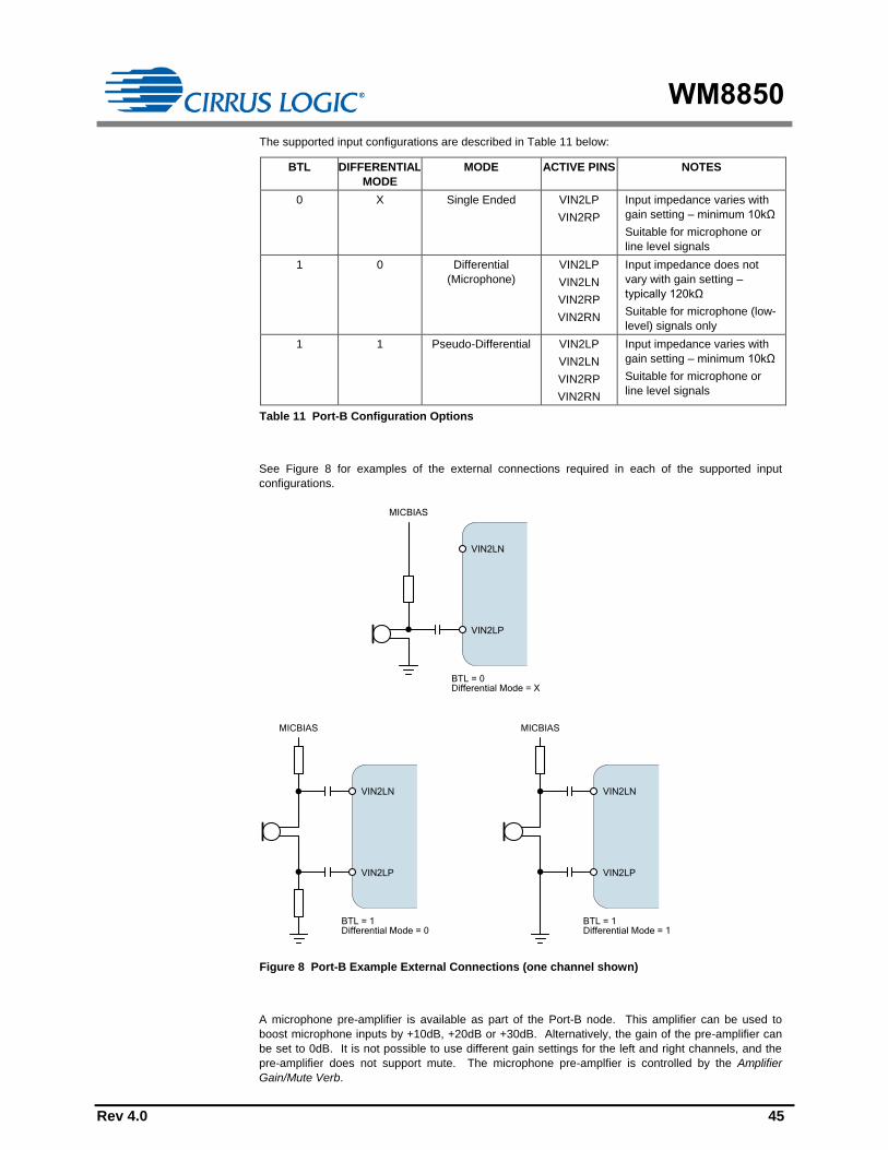
WM8850
Rev 4.0 45
The supported input configurations are described in Table 11 below:
BTL DIFFERENTIAL
MODE
MODE ACTIVE PINS NOTES
0 X Single Ended VIN2LP
VIN2RP
Input impedance varies with
gain setting – minimum 10kΩ
Suitable for microphone or
line level signals
1 0 Differential
(Microphone)
VIN2LP
VIN2LN
VIN2RP
VIN2RN
Input impedance does not
vary with gain setting –
typically 120kΩ
Suitable for microphone (low-
level) signals only
1 1 Pseudo-Differential VIN2LP
VIN2LN
VIN2RP
VIN2RN
Input impedance varies with
gain setting – minimum 10kΩ
Suitable for microphone or
line level signals
Table 11 Port-B Configuration Options
See Figure 8 for examples of the external connections required in each of the supported input
configurations.
VIN2LP
VIN2LN
MICBIAS
BTL = 0Differential Mode = X
VIN2LP
VIN2LN
MICBIAS
VIN2LP
VIN2LN
MICBIAS
BTL = 1Differential Mode = 0
BTL = 1Differential Mode = 1
Figure 8 Port-B Example External Connections (one channel shown)
A microphone pre-amplifier is available as part of the Port-B node. This amplifier can be used to
boost microphone inputs by +10dB, +20dB or +30dB. Alternatively, the gain of the pre-amplifier can
be set to 0dB. It is not possible to use different gain settings for the left and right channels, and the
pre-amplifier does not support mute. The microphone pre-amplfier is controlled by the Amplifier
Gain/Mute Verb.

WM8850
46 Rev 4.0
A low-noise microphone bias generator is provided as part of Port-B, which is suitable for use as a
bias supply for analogue microphones. The control of the microphone bias level is via the Pin Widget
Control Verb.
Port-B supports impedance sensing when using the microphone bias generator; this can be read
directly from the Pin Sense Verb. Port-B also supports presence detect, using the Pin Sense Verb.
If nothing is plugged into Port-B it is possible to use an automute function which will automatically
replace the samples in the stream with zeros, thus avoiding any noise being transmitted when there is
no input device connected. This function can be enabled using the vendor-specific Auto-Mute Control
Verb.
SET VERB BIT BITFIELD
NAME
DEFAULT DESCRIPTION
7B0h 0 PD_
AUTOMUTE
0h Auto-Mute Control:
0 = Automute disabled
1 = Automute enabled
Note: When PD_AUTOMUTE=1 and
Presence Detect (bit 31 in verb F09h)=1 the
WM8850 will replace the samples in the
stream with zeros
PGA2 (NID = 0Bh)
Table 12 gives a summary of the PGA2 node:
NODE SUMMARY INFORMATION
NID 0Ch
Widget Type Audio Selector
Supported Get Verbs Bh, F00h, F02h, FB2h
Supported Set Verbs 3h, 7B2h, 7B3h
Unsolicited Responses None
Vendor-Specific Verbs FB2h, 7B2h, 7B3h : PGA Control Verb
Table 12 PGA2 Node Summary Information
PGA2 provides analogue gain for the inputs to Port-B, allowing the signal level to be adjusted by up to
+/-12dB in 0.5dB steps. Gain can be applied to left and right channels independently if required.
Additionally, a mute function is available – again this can be applied to separate channels as required.
The gain of PGA2 is controlled using the Amplifier Gain/Mute Verb.
PGA2 uses an internal zero cross detect circuit to ensure that all gain changes occur while the signal
passes through the zero point. This function eliminates any potential DC steps that can occur if gain
changes are applied at other times, and therefore the potential for zipper noise is removed. If no zero
cross occurs within a specified time after the gain change is requested via a register write a timeout
period will elapse and the gain will be changed regardless. This timeout period can be changed using
the vendor-specific PGA Control Verb:

WM8850
Rev 4.0 47
SET VERB BIT BITFIELD
NAME
DEFAULT DESCRIPTION
7B2h
7B3h
13:0 Terminal
Count
1FFFh Set the period of the zero detect timeout clock:
0000h = Timeout disabled
0001h to 03FFh = Reserved
0400h = 1025 x 20.833µs (21.3ms)
0401h = 1026 x 20.833µs (21.4ms)
…
1FFFh = 8192 × 20.833µs (171ms)
…
3FFFh = 16384 × 20.833µs (341ms)
Note: The timeout clock uses the SYNC signal
from the HDA interface, so the absolute value
of the timeout period will depend on the
absolute accuracy of the SYNC signal.
MIC1 MUX (NID = 09h)
Table 13 gives a summary of the MIC1 Mux node:
NODE SUMMARY INFORMATION
NID 09h
Widget Type Audio Selector
Supported Get Verbs F00h, F01h, F02h
Supported Set Verbs 701h
Unsolicited Responses None
Table 13 MIC1 Mux Node Summary Information
MIC1 Mux is used to select the source of the input to the MIC1 node. This can be either from the
analogue microphone input path (from PGA2), or from the digital microphone path (from Port-D).
When the MIC1 Mux is selecting the digital microphone input (Port-D) the WM8850 is automatically
configured to bypass the analogue to digital converter part of the MIC1 node (NID = 03h).
There are no vendor-specific verbs associated with the MIC1 Mux node.
MIC1 (NID = 03H)
Table 14 gives a summary of the MIC1 node:
NODE SUMMARY INFORMATION
NID 02h
Widget Type Audio Input Converter
Supported Get Verbs Ah, F00h, F02h, F03h, F05h, F06h, F08h, F8Eh, FB1h
Supported Set Verbs 2h, 703h, 705h, 706h, 708h, 78Eh, 7B1h
Unsolicited Responses Stream Drop
Vendor-Specific Verbs F8Eh, 78Eh : Unsolicited Response Priority Control Verb
FB1h, 7B1h : Channel Copy Verb
Table 14 MIC1 Node Summary Information
MIC1 contains a high performance stereo ADC intended for capture of microphone inputs to the
WM8850. MIC1 supports all common sample rates from 8kHz to 48kHz and data widths of 16, 20, 24
and 32-bit (Float-32). The actual processing used by this node is dependant on the type of input
received from the MIC1 Mux (NID = 09h), as the input to MIC1 may come from either an analogue or
digital microphone.

WM8850
48 Rev 4.0
Regardless of the type of input, the sample rate and word length of the data captured by the MIC1
node is set using the Stream Format Verb. Table 15 below shows the required settings for Base, Mult
and Div as part of the Stream Format Verb to obtain the required sample rate.
When a digital microphone is being used, the DMICCLK output frequency will be set according to the
Stream Format Verb. See “Digital Microphone Record” for details of the DMICCLK frequency.
SAMPLE RATE BASE MULT[2:0] DIV[2:0]
8kHz 0h 0h 5h
11.025kHz 1h 0h 3h
16kHz 0h 0h 2h
22.05kHz 1h 0h 1h
32kHz 0h 1h 2h
44.1kHz 1h 0h 0h
48kHz 0h 0h 0h
Table 15 MIC1 Supported Sample Rate Settings
Note: Other settings of Base, Mult and Div are reserved and should not be set.
The MIC1 output data is by default set to provide the captured waveform from the left channel in
Channel 0, and the right channel in Channel 1. It is possible to adjust this mapping using the vendor-
specific Channel Copy Verb.
SET VERB BIT BITFIELD
NAME
DEFAULT DESCRIPTION
7B1h 1 CHAN1_
SEL
1 Channel 1 (right) Mapping Control:
0 = Channel 1 takes data from left audio
channel
1 = Channel 1 takes data from right audio
channel
0 CHAN0_
SEL
0 Channel 0 (left) Mapping Control:
0 = Channel 0 takes data from left audio
channel
1 = Channel 0 takes data from right audio
channel

WM8850
Rev 4.0 49
DIGITAL MICROPHONE RECORD
Digital microphone input is supported using the DMICDAT1, DMICDAT2 and DMICCLK pins; these
allow up to four independent digital microphones to be connected through the MIC1 and MIC2 nodes.
The digital microphone interface accepts unfiltered PDM on the DMICDAT1 and DMICDAT2 pins and
can recover data from both the high and low periods of the DMICCLK. Two microphone channels are
interleaved on DMICDAT1; another two channels are interleaved on DMICDAT2. The timing is
illustrated in Figure 9. Each microphone must tri-state its data output when the other microphone is
transmitting.
Note that the DMICDAT2 pin also supports the SPDIFOUT2 function, which is described in the
“S/PDIF Transmit” section.
DMICDAT1
DMICCLK
DATA0 DATA0Hi-Z Hi-Z
Hi-ZDMICDAT2
DMICDAT1
DMICCLK
DATA0 DATA0 DATA1DATA1
DMICDAT2 DATA2 DATA2 DATA3DATA3
Figure 9 Digital Microphone Interface Protocol for One (left) or Four (right) Microphones
The WM8850 nodes associated with this function are shown in Figure 10.
MIC1
03h
MIC1 Mux
09h
MIC2
15h
Port-H
16h
Port-D
0Eh
DMICDAT1
DMICCLK
DMICDAT2/SPDIFOUT2
HD
A In
terf
ace
from S/PDIF In
from S/PDIF Tx 2
from PGA2
Figure 10 Digital Microphone Record Path
This section provides a summary of the Port-D, Port-H and MIC2 nodes, and describes the vendor-
specific verb functions associated with each.
The MIC1 Mux and MIC1 nodes are described in the “Stereo Analogue Microphone Record” section.
WM8850
50 Rev 4.0
PORT-D (NID = 0Eh)
Table 16 gives a summary of the Port-D node:
NODE SUMMARY INFORMATION
NID 0Eh
Widget Type Pin Complex
Supported Get Verbs Bh, F00h, F07h, F1Ch
Supported Set Verbs 3h, 707h, 71Ch, 71Dh, 71Eh, 71Fh
Unsolicited Responses None
Table 16 Port-D Node Summary Information
Port-D provides digital gain for the microphone(s) connected to DMICDAT1, allowing the signal level
to be adjusted by up to +32dB to −12dB in 0.5dB steps. Gain can be applied to left and right
channels independently if required. Additionally, a mute function is available – again this can be
applied to separate channels as required. The gain is controlled using the Amplifier Gain/Mute Verb.
There are no vendor-specific verbs associated with the Port-D node.
PORT-H (NID = 16H)
Table 17 gives a summary of the Port-H node:
NODE SUMMARY INFORMATION
NID 16h
Widget Type Pin Complex
Supported Get Verbs Bh, F00h, F02h, F07h, F1Ch, F73h
Supported Set Verbs 3h, 707h, 71Ch, 71Dh, 71Eh, 71Fh, 773h
Unsolicited Responses None
Vendor-Specific Verbs F73h, 773h : Internal Path Verb
Table 17 Port-H Node Summary Information
Port-H provides digital gain for the microphone(s) connected to DMICDAT2, allowing the signal level
to be adjusted by up to +32dB to −12dB in 0.5dB steps. Gain can be applied to left and right
channels independently if required. Additionally, a mute function is available – again this can be
applied to separate channels as required. The gain is controlled using the Amplifier Gain/Mute Verb.
Note that Port-H can also be used to provide a S/PDIF output. For details of the use of the node as a
S/PDIF output, see the “S/PDIF Transmit” section.
When Port-H is configured for S/PDIF output, it is possible to select either S/PDIF In or S/PDIF Tx 2
as the data source. The signal path is selected using vendor-specific Internal Path Verb.
SET VERB BIT BITFIELD
NAME
DEFAULT DESCRIPTION
773h 7:0 Path Sel 17h Selects the source of the Port-H node:
10h = S/PDIF In
17h = S/PDIF Tx2
WM8850
Rev 4.0 51
MIC2 (NID = 15h)
Table 18 gives a summary of the MIC2 node:
NODE SUMMARY INFORMATION
NID 15h
Widget Type Audio Input Converter
Supported Get Verbs Ah, F00h, F02h, F03h, F06h, F08h, F8Eh, FB1h
Supported Set Verbs 703h, 706h, 708h, 78Eh, 7B1h
Unsolicited Responses Stream Drop
Vendor-Specific Verbs F8Eh, 78Eh : Unsolicited Response Priority Control Verb
FB1h, 7B1h : Channel Copy Verb
Table 18 MIC2 Node Summary Information
The MIC2 node supports digital audio input at all common sample rates from 8kHz to 48kHz.
Note that the Stream Format Verb in the MIC2 widget (NID = 15h) is read-only; the associated
parameters will echo the values set in the same verb in the MIC1 widget.
The MIC2 output data is by default set to provide the captured waveform from the left channel in
Channel 0, and the right channel in Channel 1. It is possible to adjust this mapping using the vendor-
specific Channel Copy Verb:
SET VERB BIT BITFIELD
NAME
DEFAULT DESCRIPTION
7B1h 1 CHAN1_
SEL
1 Channel 1 (right) Mapping Control:
0 = Channel 1 takes data from left audio
channel
1 = Channel 1 takes data from right audio
channel
0 CHAN0_
SEL
0 Channel 0 (left) Mapping Control:
0 = Channel 0 takes data from left audio
channel
1 = Channel 0 takes data from right audio
channel
DIGITAL MICROPHONE INTERFACE CLOCK RATES
The sample rate of data captured by the digital microphone interface is controlled by the Stream
Format Verb in the MIC1 widget (NID = 03h). Note that the Stream Format Verb in the MIC2 widget
(NID = 15h) will echo the values set in the same verb in the MIC1 widget. This is necessary as
DMICCLK is shared between the DMICDAT1 and DMICDAT2 pins.
The DMICCLK frequency will output at the rates shown in Table 19, which also contains the required
settings for Base, Mult and Div as part of the Stream Format Verb of the MIC1 widget to obtain the
required sample rate:
SAMPLE RATE BASE MULT[2:0] DIV[2:0] DMICCLK
FREQUENCY
PROCESSING
RATE
8kHz 0h 0h 5h 1.024MHz 128fs
11.025kHz 1h 0h 3h 1.4112MHz 128fs
16kHz 0h 0h 2h 1.024MHz 64fs
22.05kHz 1h 0h 1h 1.4112MHz 64fs
32kHz 0h 1h 2h 2.048MHz 64fs
44.1kHz 1h 0h 0h 2.8224MHz 64fs
48kHz 0h 0h 0h 3.072MHz 64fs
Table 19 MIC1 Supported Sample Rate Settings for Digital Microphone Interface
Note: Other settings of Base, Mult and Div are reserved and should not be set.

WM8850
52 Rev 4.0
STEREO HEADPHONE PLAYBACK
Stereo headphone playback is supported using the VOUT1L and VOUT1R pins; these provide a
ground-referenced stereo output through the DAC1 node. This output is intended for headphones,
but can be used as a single-ended line output if required. This path can provide two channels of a
multi-channel playback system, operating alongside the other two DAC paths.
It is possible to configure the stereo headphone outputs to select the S/PDIF Rx node as the data
source. This signal path is enabled using a vendor-specific verb, and is illustrated by the dotted line in
Figure 11.
The WM8850 nodes associated with this function are shown in Figure 11.
DAC1
06h
Port-A
11h
VOUT1L
VOUT1R
from S/PDIF Rx
HD
A In
terf
ace
Figure 11 Stereo Headphone Playback Path
This section provides a summary of the DAC1 and Port-A, and describes the vendor-specific verb
functions associated with each.
DAC1 (NID = 06H)
Table 20 gives a summary of the DAC1 node:
NODE SUMMARY INFORMATION
NID 06h
Widget Type Audio Converter
Supported Get Verbs Ah, Bh, F00h, F05h, F06h, F08h, F73h, F8Eh
Supported Set Verbs 2h, 3h, 705h, 706h, 708h, 773h, 78Eh
Unsolicited Responses Stream Error
Vendor-Specific Verbs F73h, 773h : Internal Path Verb
F8Eh, 78Eh : Unsolicited Response Priority Control Verb
Table 20 DAC1 Node Summary Information
DAC1 is a high performance stereo DAC that supports all common sample rates from 8kHz to
192kHz and data widths of 16, 20, 24 and 32-bit (Float-32).
The sample rate and word length of the data played back by the DAC1 node is set using the Stream
Format Verb. Table 9 below shows the required settings for Base, Mult and Div as part of the Stream
Format Verb to obtain the required sample rate.
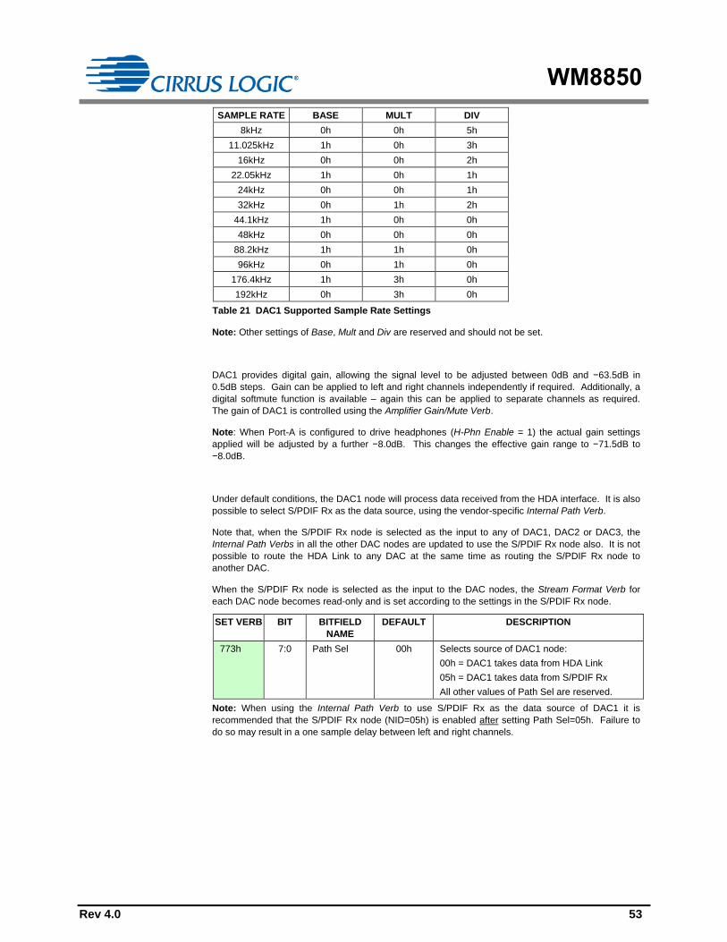
WM8850
Rev 4.0 53
SAMPLE RATE BASE MULT DIV
8kHz 0h 0h 5h
11.025kHz 1h 0h 3h
16kHz 0h 0h 2h
22.05kHz 1h 0h 1h
24kHz 0h 0h 1h
32kHz 0h 1h 2h
44.1kHz 1h 0h 0h
48kHz 0h 0h 0h
88.2kHz 1h 1h 0h
96kHz 0h 1h 0h
176.4kHz 1h 3h 0h
192kHz 0h 3h 0h
Table 21 DAC1 Supported Sample Rate Settings
Note: Other settings of Base, Mult and Div are reserved and should not be set.
DAC1 provides digital gain, allowing the signal level to be adjusted between 0dB and −63.5dB in
0.5dB steps. Gain can be applied to left and right channels independently if required. Additionally, a
digital softmute function is available – again this can be applied to separate channels as required.
The gain of DAC1 is controlled using the Amplifier Gain/Mute Verb.
Note: When Port-A is configured to drive headphones (H-Phn Enable = 1) the actual gain settings
applied will be adjusted by a further −8.0dB. This changes the effective gain range to −71.5dB to
−8.0dB.
Under default conditions, the DAC1 node will process data received from the HDA interface. It is also
possible to select S/PDIF Rx as the data source, using the vendor-specific Internal Path Verb.
Note that, when the S/PDIF Rx node is selected as the input to any of DAC1, DAC2 or DAC3, the
Internal Path Verbs in all the other DAC nodes are updated to use the S/PDIF Rx node also. It is not
possible to route the HDA Link to any DAC at the same time as routing the S/PDIF Rx node to
another DAC.
When the S/PDIF Rx node is selected as the input to the DAC nodes, the Stream Format Verb for
each DAC node becomes read-only and is set according to the settings in the S/PDIF Rx node.
SET VERB BIT BITFIELD
NAME
DEFAULT DESCRIPTION
773h 7:0 Path Sel 00h Selects source of DAC1 node:
00h = DAC1 takes data from HDA Link
05h = DAC1 takes data from S/PDIF Rx
All other values of Path Sel are reserved.
Note: When using the Internal Path Verb to use S/PDIF Rx as the data source of DAC1 it is
recommended that the S/PDIF Rx node (NID=05h) is enabled after setting Path Sel=05h. Failure to
do so may result in a one sample delay between left and right channels.

WM8850
54 Rev 4.0
PORT-A (NID = 11H)
Table 22 gives a summary of the Port-A node:
NODE SUMMARY INFORMATION
NID 11h
Widget Type Pin Complex
Supported Get Verbs F00h, F02h, F07h, F08h, F09h, F1Ch, F8Eh
Supported Set Verbs 707h, 708h, 709h, 71Ch, 71Dh, 71Eh, 71Fh, 78Eh
Unsolicited Responses Presence Detect
Vendor-Specific Verbs F8Eh, 78Eh : Unsolicited Response Priority Control Verb
Table 22 Port-A Node Summary Information
Port-A contains a ground-referenced headphone driver which negates the requirement for large AC-
coupling capacitors commonly required for headphone applications. The headphone driver is
powered by an on-board charge pump which generates the required positive and negative supply
voltages. Configuration of this block is handled automatically by the WM8850, and the required
external components to enable optimum performance of the charge pump are given in the
“Applications Information” section.

WM8850
Rev 4.0 55
STEREO LINE PLAYBACK
Stereo line playback is supported using the VOUT2LP, VOUT2LN, VOUT2RP and VOUT2RN pins;
these provide a differential stereo output through the DAC2 node. These outputs are intended for
line-level loads; the differential configuration provides noise rejection, particularly in the case of
lengthy signal tracks. An external differential to single-ended converter should be used for connection
to an external stereo jack. This path can provide two channels of a multi-channel playback system,
operating alongside the other two DAC paths.
Stereo line playback is also supported using the VOUT3LP, VOUT3LN, VOUT3RP and VOUT3RN
pins; these provide a differential stereo output through the DAC3 node. This path is identical in
function to the DAC2 path, so both paths are described together here. Note, however, that they are
completely independent paths and must be setup separately.
It is possible to configure either of the stereo line outputs to select the S/PDIF Rx node as the data
source. These signal paths are enabled using vendor-specific verbs, and are illustrated by the dotted
line in Figure 12.
The WM8850 nodes associated with this function are shown in Figure 12.
DAC2
07h
Port-G
12h
Port-F
13h
DAC3
08h
VOUT2LP
VOUT2LN
VOUT2RP
VOUT2RN
VOUT3LP
VOUT3LN
VOUT3RP
VOUT3RN
from S/PDIF Rx
from S/PDIF Rx
HD
A In
terf
ace
Figure 12 Stereo Differential Line Playback Paths
This section provides a summary of the DAC2, Port-G, DAC3 and Port-F nodes, and describes the
vendor-specific verb functions associated with each.
DAC2 (NID = 07h) AND DAC3 (NID = 08h)
Table 23 gives a summary of the DAC2 and DAC3 nodes:
NODE SUMMARY INFORMATION
NID 07h / 08h
Widget Type Audio Converter
Supported Get Verbs Ah, Bh, F00h, F05h, F06h, F08h, F73h, F8Eh
Supported Set Verbs 2h, 3h, 705h, 706h, 708h, 773h, 78Eh
Unsolicited Responses Stream Error
Vendor-Specific Verbs F73h, 773h : Internal Path Verb
F8Eh, 78Eh : Unsolicited Response Priority Control Verb
Table 23 DAC2 and DAC3 Nodes Summary Information
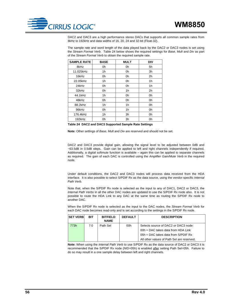
WM8850
56 Rev 4.0
DAC2 and DAC3 are a high performance stereo DACs that supports all common sample rates from
8kHz to 192kHz and data widths of 16, 20, 24 and 32-bit (Float-32).
The sample rate and word length of the data played back by the DAC2 or DAC3 nodes is set using
the Stream Format Verb. Table 24 below shows the required settings for Base, Mult and Div as part
of the Stream Format Verb to obtain the required sample rate.
SAMPLE RATE BASE MULT DIV
8kHz 0h 0h 5h
11.025kHz 1h 0h 3h
16kHz 0h 0h 2h
22.05kHz 1h 0h 1h
24kHz 0h 0h 1h
32kHz 0h 1h 2h
44.1kHz 1h 0h 0h
48kHz 0h 0h 0h
88.2kHz 1h 1h 0h
96kHz 0h 1h 0h
176.4kHz 1h 3h 0h
192kHz 0h 3h 0h
Table 24 DAC2 and DAC3 Supported Sample Rate Settings
Note: Other settings of Base, Mult and Div are reserved and should not be set.
DAC2 and DAC3 provide digital gain, allowing the signal level to be adjusted between 0dB and
−63.5dB in 0.5dB steps. Gain can be applied to left and right channels independently if required.
Additionally, a digital softmute function is available – again this can be applied to separate channels
as required. The gain of each DAC is controlled using the Amplifier Gain/Mute Verb in the required
node.
Under default conditions, the DAC2 and DAC3 nodes will process data received from the HDA
interface. It is also possible to select S/PDIF Rx as the data source, using the vendor-specific Internal
Path Verb.
Note that, when the S/PDIF Rx node is selected as the input to any of DAC1, DAC2 or DAC3, the
Internal Path Verbs in all the other DAC nodes are updated to use the S/PDIF Rx node also. It is not
possible to route the HDA Link to any DAC at the same time as routing the S/PDIF Rx node to
another DAC.
When the S/PDIF Rx node is selected as the input to the DAC nodes, the Stream Format Verb for
each DAC node becomes read-only and is set according to the settings in the S/PDIF Rx node.
SET VERB BIT BITFIELD
NAME
DEFAULT DESCRIPTION
773h 7:0 Path Sel 00h Selects source of DAC2 or DAC3 node:
00h = DAC takes data from HDA Link
05h = DAC takes data from S/PDIF Rx
All other values of Path Sel are reserved.
Note: When using the Internal Path Verb to use S/PDIF Rx as the data source of DAC2 or DAC3 it is
recommended that the S/PDIF Rx node (NID=05h) is enabled after setting Path Sel=05h. Failure to
do so may result in a one sample delay between left and right channels.

WM8850
Rev 4.0 57
PORT-G (NID = 12h) AND PORT-F (NID = 13h)
Table 25 gives a summary of the Port-G and Port-F nodes:
NODE SUMMARY INFORMATION
NID 12h / 13h
Widget Type Pin Complex
Supported Get Verbs F00h, F02h, F07h, F08h, F09h, F1Ch, F8Eh
Supported Set Verbs 707h, 708h, 709h, 71Ch, 71Dh, 71Eh, 71Fh, 78Eh
Unsolicited Responses Presence Detect
Vendor-Specific Verbs F8Eh, 78Eh : Unsolicited Response Priority Control Verb
Table 25 Port-G and Port-F Nodes Summary Information
Port-G and Port-F each contain a VMID-referenced differential line driver which requires AC-coupling
if driving outputs directly. It is possible to use the output in a single-ended configuration if required;
note that this will result in a drop in signal level of 6dB.
If a single-ended output is required, VOUT2LP (VOUT3LP) and VOUT2RP (VOUT3RP) should be
used to connect to the load, and VOUT2LN (VOUT3LN) and VOUT2RN (VOUT3RN) should be left
unconnected. There is no requirement to change register settings or provide any additional external
components to compensate for the unconnected output pins.

WM8850
58 Rev 4.0
S/PDIF RECEIVE
S/PDIF Receive functionality is supported using the SPDIFIN pin; this provides an IEC-60958-3
compatible S/PDIF input through the S/PDIF Rx node.
The S/PDIF receiver accepts all common audio sample frequencies from 32kHz to 96kHz, and an on-
chip fully-asynchronous sample rate coverter (SRC) provides the flexibility to interface any supported
incoming S/PDIF rate to the HDA interface without loss of quality. The S/PDIF receiver supports
readback of all 40-bits of the S/PDIF channel status information, but does not decode the user
channel data.
The WM8850 nodes associated with this function are shown in Figure 13:
S/PDIF Rx
05h
S/PDIF
In
10h
SPDIFIN
HD
A In
terf
ace
Figure 13 S/PDIF Receive Path
This section provides a summary of the S/PDIF In and S/PDIF Rx nodes, and describes the vendor-
specific verb functions associated with each.
S/PDIF IN (NID = 10h)
Table 26 gives a summary of the S/PDIF In node:
NODE SUMMARY INFORMATION
NID 10h
Widget Type Pin Complex
Supported Get Verbs F00h, F07h, F08h, F09h, F1Ch, F8Eh, FA0h, FA1h
Supported Set Verbs 707h, 708h, 71Ch, 71Dh, 71Eh, 71Fh, 78Eh, 7A1h
Unsolicited Responses Presence Detect
Lock Status
Recovered Rate Change
Vendor-Specific Verbs F8Eh, 78Eh : Unsolicited Response Priority Control Verb
FA0h : Get S/PDIF In Status Verb
FA1h, 7Ah : S/PDIF In Control Verb
Table 26 S/PDIF In Node Summary Information
The S/PDIF In node provides control over the physical connection of the input to the S/PDIF receiver.
The node also provides basic status information from the S/PDIF receiver circuitry, such as lock
status and recovered sample rate.
The S/PDIF input circuitry accepts signal levels as described in IEC-60958-3, as well as CMOS
compatible and low-amplitude CMOS compatible signals. This allows for a wide range of external
connectivity to the WM8850 depending on the application, which may range from direct connection of
electrical signals from a coaxial cable through a matching network or from another CMOS device like
an optical receiver or DSP.

WM8850
Rev 4.0 59
The input configuration for the SPDIFIN pin is controlled by two register bits in the vendor-specific Get
S/PDIF In Control Verb.
SET VERB BIT BITFIELD
NAME
DEFAULT DESCRIPTION
7A1h 1 CMOS
Thres
0 Selects the logic threshold levels when in
CMOS Mode:
0 = 30% / 70% thresholds
1 = 20% / 40% thresholds
0 Pin Mode
Sel
0 Selects the SPDIFIN Pin mode:
0 = CMOS Mode
1 = Comparator Mode
See Figure 14 for examples of the external connections required in each of the supported S/PDIF
input modes:
SPDIFIN
75Ω
Pin Mode Sel = 1
500mVpp IEC-60958-3 compatible signalSPDIFIN
Pin Mode Sel = 0
CMOS Device
Figure 14 SPDIFIN Example External Connections
The vendor-specific S/PDIF In Status Verb can be used to see the current physical status of the
S/PDIF receiver. This verb indicates whether the S/PDIF Receiver circuitry is locked, and the sample
rate of the incoming S/PDIF stream.
GET VERB BIT BITFIELD
NAME
DEFAULT DESCRIPTION
FA0h 3:1 RATE 7h Recovered sample rate:
0h = Reserved
1h = Reserved
2h = 96 kHz
3h = 88.2 kHz
4h = 48 kHz
5h = 44.1 kHz
6h = 32 kHz
7h = Sample rate not detected
0 LOCK 0 S/PDIF Rx lock flag:
0 = Unlocked
1 = Locked
Note: The RATE value is measured directly from the incoming S/PDIF stream, using the BCLK on the
HDA link as a reference clock. The reported sample rate in the channel status of the S/PDIF stream
is not used to provide this value, so in a situation where the two differ the RATE value in the will
reflect the actual sample rate of the S/PDIF input signal. This assumes that the speed of the BCLK
on the HDA link is within the acceptable tolerance as defined in the HDA Specification.

WM8850
60 Rev 4.0
If the S/PDIF receiver unlocks and the relocks once a stream is setup, for example as a result of a
change in the rate of the S/PDIF signal applied to SPDIFIN pin, then the WM8850 can be configured
to behave in two ways:
Push Method
As soon as the S/PDIF Rx loses lock the stream is overwritten with zeros at the previously received
sample rate. Once the S/PDIF Rx achieves lock again the zeros will be removed and the recovered
samples will be output at the new sample rate. This is the default behaviour for the WM8850.
When configured for the push method it is still possible for the controller to terminate the stream while
the S/PDIF Rx is unlocked by setting the Stream ID to 0. The stream will then not be restarted until
the Stream ID has been assigned a new (non-zero) number and the S/PDIF Rx has achieved lock
again.
Controlled Method
As soon as the S/PDIF Rx loses lock the stream is overwritten with zeros at the previous received
sample rate. This will continue until the stream is terminated by the controller by setting the Stream
ID to 0, even if the S/PDIF Rx regains lock. The stream will not be restarted until the Stream ID has
been assigned a new (non-zero) number and the S/PDIF Rx has achieved lock again.
The controlled method protects against a change in the stream sample rate while the stream is active.
The S/PDIF receiver unlock behaviour is selected using the S/PDIF In Control Verb.
SET VERB BIT BITFIELD
NAME
DEFAULT DESCRIPTION
7A1h 3 Unlock Ctrl 0 S/PDIF In unlock control:
0 = Push method
1 = Controlled method
As the S/PDIF In node does not support presence detect as defined in the HDA specification, by
default it will report Presence Detect Capable=0 in the Pin Capabilities Parameter. However, it is
possible to use the lock status of the S/PDIF Rx to indicate that something is plugged into S/PDIF In
using the vendor-specific S/PDIF In Control Verb. If this feature is enabled the S/PDIF In node will
report Presence Detect Capable=1 in the Pin Capabilities Parameter, will support the Pin Sense Verb
and be able to generate an unsolicited response based on the presence detect value in the Pin Sense
Verb if this functionality is set in the Unsolicited Response Verb.
SET VERB BIT BITFIELD
NAME
DEFAULT DESCRIPTION
7A1h 2 PD Config 0 Configures the Presence Detect Capable
parameter:
0 = Do not use lock status as presence detect
1 = Use lock status as presence detect

WM8850
Rev 4.0 61
S/PDIF RX (NID = 05h)
Table 27 gives a summary of the S/PDIF Rx node:
NODE SUMMARY INFORMATION
NID 05h
Widget Type Audio Input
Supported Get Verbs Ah, F00h, F02h, F03h, F06h, F08h, F0Dh, F80h, F8Eh, F91h,
F92h, F93h
Supported Set Verbs 2h, 703h, 706h, 708h, 70Dh, 78Eh, 793h
Unsolicited Responses Stream Drop
Sample Drop
SRC1 Lock Status Change
Digital Converter Register Update
Validity Flag Status Change
Channel Status Update
Non-Audio Flag Status Change
Data Receive Error
Vendor-Specific Verbs F80h : S/PDIF Verb
F8Eh, 78Eh : Unsolicited Response Priority Control Verb
F91h : Get Channel Status Verb
F92h : Get Non-Audio Flag Verb
F93h, 793h : Sample Overwrite Control Verb
Table 27 S/PDIF Rx Node Summary Information
The S/PDIF Rx node provides control over the S/PDIF receiver circuitry and the optional SRC1
processing stage. The S/PDIF receiver measures the actual sample rate of the incoming S/PDIF
signal, recovers the payload data and decodes channel status information. The recovered data can
then be passed through SRC1 (Sample Rate Converter) if necessary to interface to the HDA link
domain.
The Digital Converter Verb is supported by the S/PDIF Rx node, allowing readback of selected
channel status information as defined in the HDA Specification. It is also possible to readback all 40-
bits of the channel status data as defined in IEC-60958-3, using the vendor-specific Get Channel
Status Verb.

WM8850
62 Rev 4.0
GET VERB BIT BITFIELD
NAME
DEFAULT DESCRIPTION
F91h 39:36 Original
Sampling
Frequency
N/A Original Sampling Frequency
35:33 Sample
Word Length
N/A Sample Word Length
32 Max Word
Length
N/A Max Word Length
31:28 Clock
Accuracy
N/A Clock Accuracy
27:24 Sampling
Frequency
N/A Sampling Frequency
23:20 Channel
Number
N/A Channel Number
19:16 Source
Number
N/A Source Number
15:8 Category
Code
N/A Category Code
7:6 Channel
Status Mode
N/A Channel Status Mode
5:4 Additional
De-
emphasis
Information
N/A Additional De-emphasis Information
3 PRE N/A Pre-emphasis
2 /COPY N/A Copyright
1 /AUDIO N/A Non Audio
0 PRO N/A Professional/Consumer
Notes:
1. [31:0] are returned when Payload[7:0] = 00h, [39:32] are returned when Payload[7:0] = 01h
2. See IEC-60958-3 for full definitions of the channel status bits
The /AUDIO flag in the channel status for the S/PDIF stream is set by the source of the S/PDIF data
to indicate that the data samples within the S/PDIF stream are not audio PCM samples. In addition,
IEC-61937 specifies a non-audio sync code which can be detected by the WM8850. The WM8850
provides a Non Audio Flag to indicate if the non-audio code has been detected. The Non Audio Flag
can be readback using the vendor-specific Get Non-Audio Flag Verb.
GET VERB BIT BITFIELD
NAME
DEFAULT DESCRIPTION
F92h 0 Non Audio
Flag
0 Indicates the presence of the Non Audio Flag:
0 = Non Audio Flag not asserted
1 = Non Audio Flag asserted
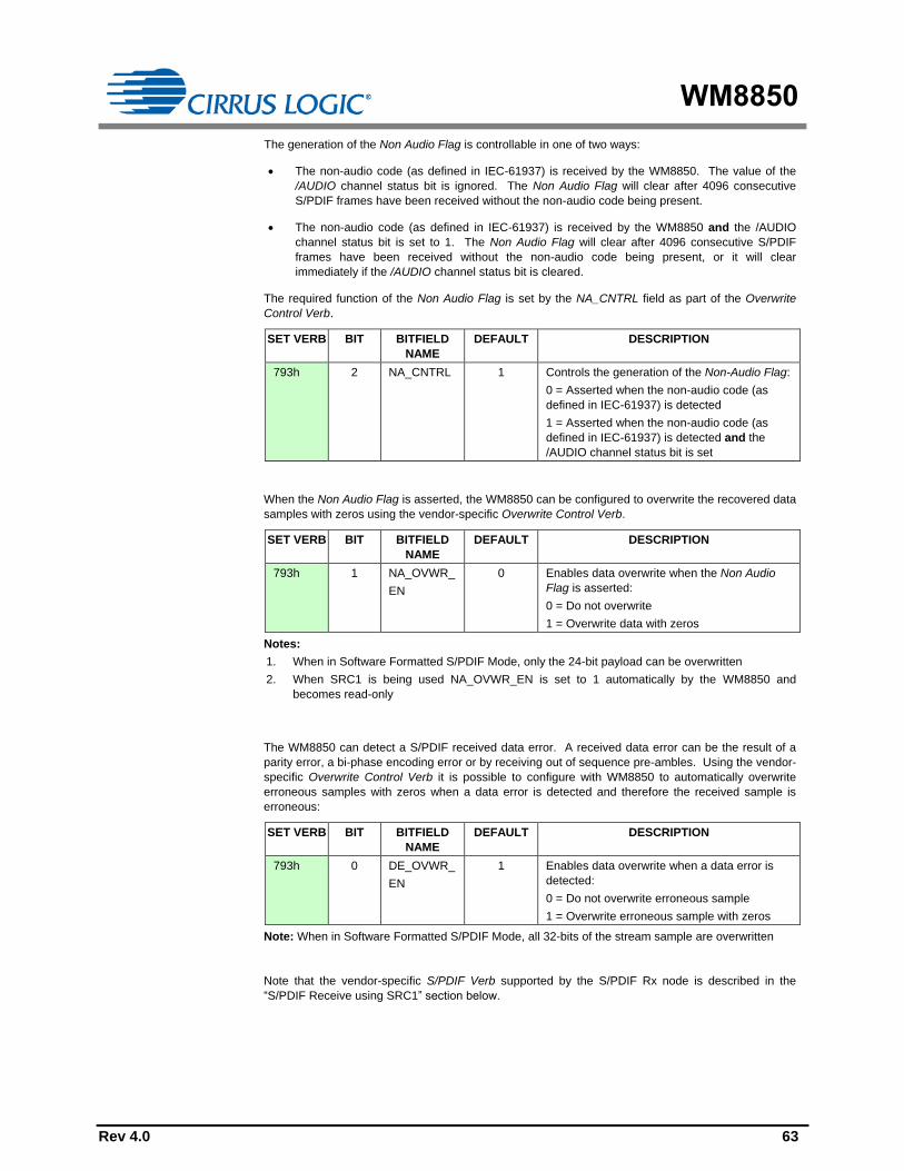
WM8850
Rev 4.0 63
The generation of the Non Audio Flag is controllable in one of two ways:
The non-audio code (as defined in IEC-61937) is received by the WM8850. The value of the
/AUDIO channel status bit is ignored. The Non Audio Flag will clear after 4096 consecutive
S/PDIF frames have been received without the non-audio code being present.
The non-audio code (as defined in IEC-61937) is received by the WM8850 and the /AUDIO
channel status bit is set to 1. The Non Audio Flag will clear after 4096 consecutive S/PDIF
frames have been received without the non-audio code being present, or it will clear
immediately if the /AUDIO channel status bit is cleared.
The required function of the Non Audio Flag is set by the NA_CNTRL field as part of the Overwrite
Control Verb.
SET VERB BIT BITFIELD
NAME
DEFAULT DESCRIPTION
793h 2 NA_CNTRL 1 Controls the generation of the Non-Audio Flag:
0 = Asserted when the non-audio code (as
defined in IEC-61937) is detected
1 = Asserted when the non-audio code (as
defined in IEC-61937) is detected and the
/AUDIO channel status bit is set
When the Non Audio Flag is asserted, the WM8850 can be configured to overwrite the recovered data
samples with zeros using the vendor-specific Overwrite Control Verb.
SET VERB BIT BITFIELD
NAME
DEFAULT DESCRIPTION
793h 1 NA_OVWR_
EN
0 Enables data overwrite when the Non Audio
Flag is asserted:
0 = Do not overwrite
1 = Overwrite data with zeros
Notes:
1. When in Software Formatted S/PDIF Mode, only the 24-bit payload can be overwritten
2. When SRC1 is being used NA_OVWR_EN is set to 1 automatically by the WM8850 and
becomes read-only
The WM8850 can detect a S/PDIF received data error. A received data error can be the result of a
parity error, a bi-phase encoding error or by receiving out of sequence pre-ambles. Using the vendor-
specific Overwrite Control Verb it is possible to configure with WM8850 to automatically overwrite
erroneous samples with zeros when a data error is detected and therefore the received sample is
erroneous:
SET VERB BIT BITFIELD
NAME
DEFAULT DESCRIPTION
793h 0 DE_OVWR_
EN
1 Enables data overwrite when a data error is
detected:
0 = Do not overwrite erroneous sample
1 = Overwrite erroneous sample with zeros
Note: When in Software Formatted S/PDIF Mode, all 32-bits of the stream sample are overwritten
Note that the vendor-specific S/PDIF Verb supported by the S/PDIF Rx node is described in the
“S/PDIF Receive using SRC1” section below.
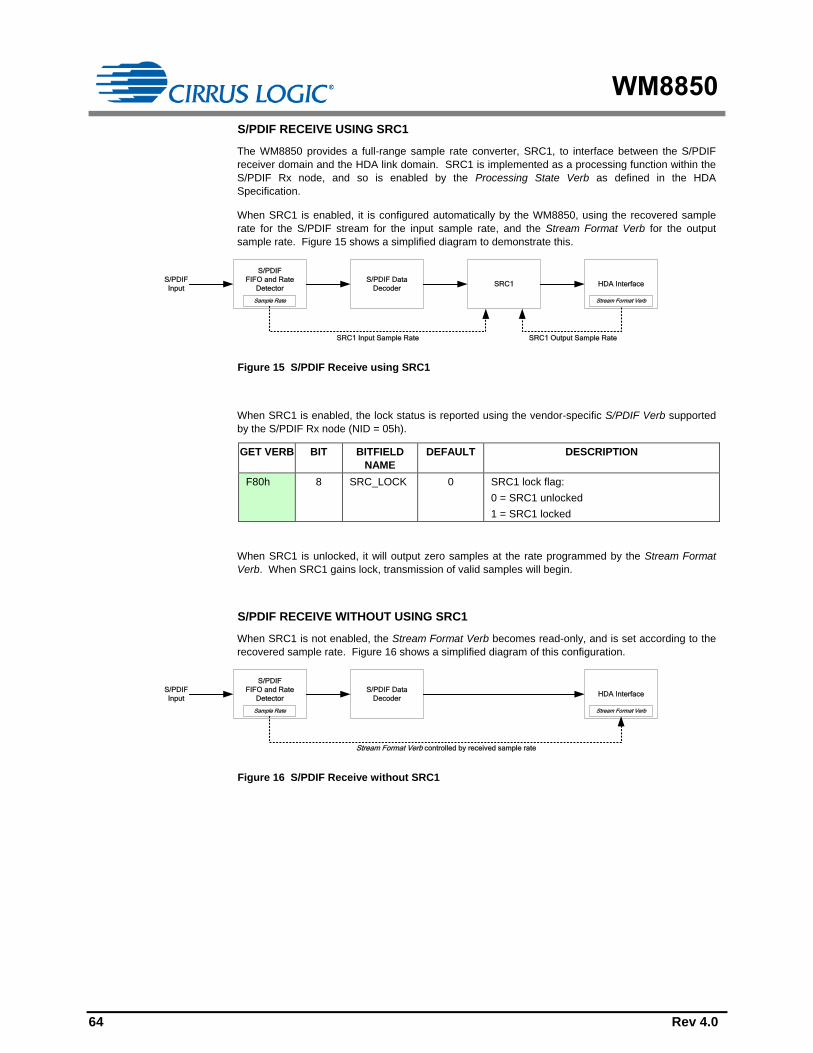
WM8850
64 Rev 4.0
S/PDIF RECEIVE USING SRC1
The WM8850 provides a full-range sample rate converter, SRC1, to interface between the S/PDIF
receiver domain and the HDA link domain. SRC1 is implemented as a processing function within the
S/PDIF Rx node, and so is enabled by the Processing State Verb as defined in the HDA
Specification.
When SRC1 is enabled, it is configured automatically by the WM8850, using the recovered sample
rate for the S/PDIF stream for the input sample rate, and the Stream Format Verb for the output
sample rate. Figure 15 shows a simplified diagram to demonstrate this.
S/PDIF
FIFO and Rate
Detector
S/PDIF Data
DecoderHDA InterfaceSRC1
S/PDIF
Input
SRC1 Input Sample Rate SRC1 Output Sample Rate
Stream Format VerbSample Rate
Figure 15 S/PDIF Receive using SRC1
When SRC1 is enabled, the lock status is reported using the vendor-specific S/PDIF Verb supported
by the S/PDIF Rx node (NID = 05h).
GET VERB BIT BITFIELD
NAME
DEFAULT DESCRIPTION
F80h 8 SRC_LOCK 0 SRC1 lock flag:
0 = SRC1 unlocked
1 = SRC1 locked
When SRC1 is unlocked, it will output zero samples at the rate programmed by the Stream Format
Verb. When SRC1 gains lock, transmission of valid samples will begin.
S/PDIF RECEIVE WITHOUT USING SRC1
When SRC1 is not enabled, the Stream Format Verb becomes read-only, and is set according to the
recovered sample rate. Figure 16 shows a simplified diagram of this configuration.
S/PDIF
FIFO and Rate
Detector
S/PDIF Data
DecoderHDA Interface
S/PDIF
Input
Stream Format Verb controlled by received sample rate
Stream Format VerbSample Rate
Figure 16 S/PDIF Receive without SRC1

WM8850
Rev 4.0 65
S/PDIF RECEIVE TO DACS
It is possible to select S/PDIF Rx as the data source for the DACs on the WM8850, as described in
the “Stereo Headphone Playback” and “Stereo Line Playback” sections.
In this mode, SRC1 is bypassed, the Stream Format Verb in each of the DAC nodes becomes read-
only and are set according to the recovered sample rate. Figure 17 shows a simplified diagram of this
configuration.
S/PDIF
FIFO and Rate
Detector
S/PDIF Data
DecoderDAC2
S/PDIF
Input
Stream Format Verbs controlled by received sample rate
Stream Format VerbSample Rate
DAC1
Stream Format Verb
DAC3
Stream Format Verb
Figure 17 S/PDIF Receive to DACs
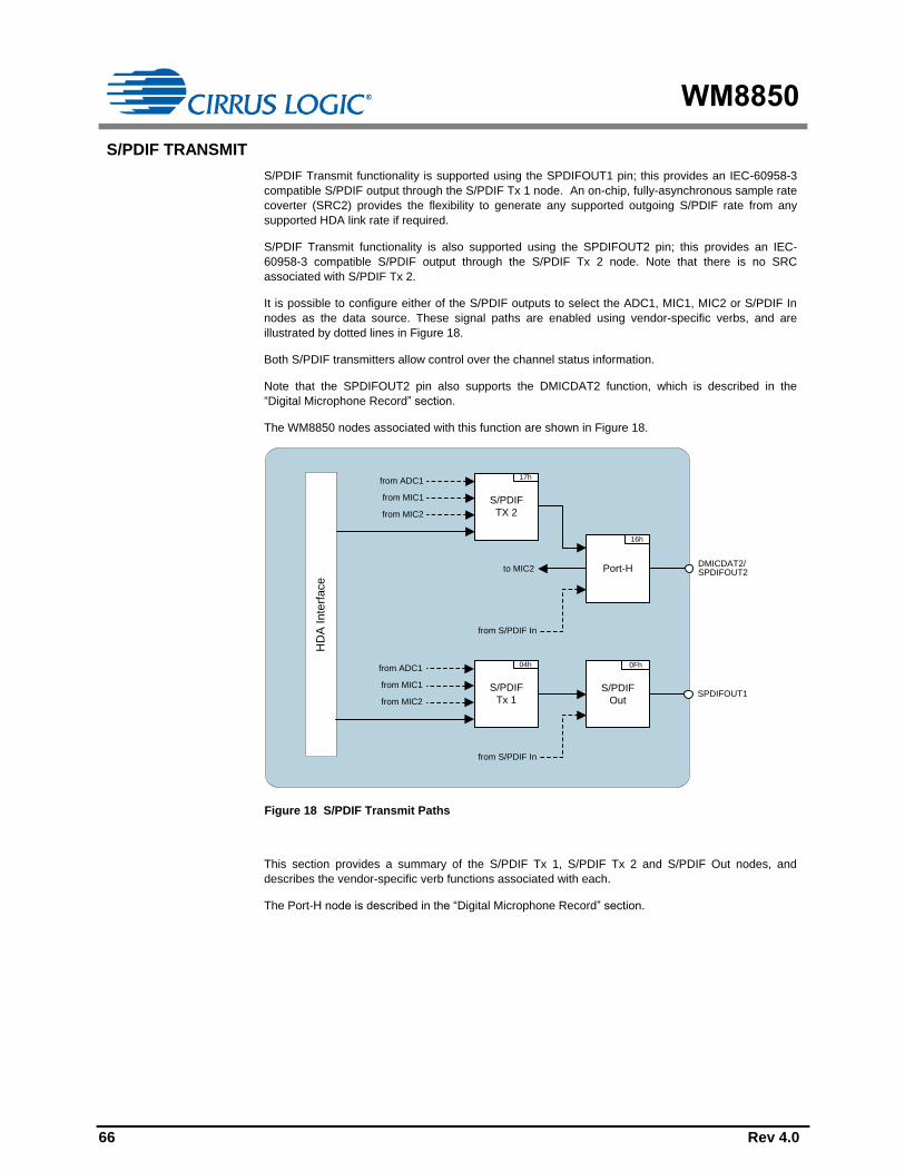
WM8850
66 Rev 4.0
S/PDIF TRANSMIT
S/PDIF Transmit functionality is supported using the SPDIFOUT1 pin; this provides an IEC-60958-3
compatible S/PDIF output through the S/PDIF Tx 1 node. An on-chip, fully-asynchronous sample rate
coverter (SRC2) provides the flexibility to generate any supported outgoing S/PDIF rate from any
supported HDA link rate if required.
S/PDIF Transmit functionality is also supported using the SPDIFOUT2 pin; this provides an IEC-
60958-3 compatible S/PDIF output through the S/PDIF Tx 2 node. Note that there is no SRC
associated with S/PDIF Tx 2.
It is possible to configure either of the S/PDIF outputs to select the ADC1, MIC1, MIC2 or S/PDIF In
nodes as the data source. These signal paths are enabled using vendor-specific verbs, and are
illustrated by dotted lines in Figure 18.
Both S/PDIF transmitters allow control over the channel status information.
Note that the SPDIFOUT2 pin also supports the DMICDAT2 function, which is described in the
“Digital Microphone Record” section.
The WM8850 nodes associated with this function are shown in Figure 18.
S/PDIF
TX 2
17h
S/PDIF
Tx 1
04h
S/PDIF
Out
0Fh
Port-H
16h
DMICDAT2/SPDIFOUT2
SPDIFOUT1
from ADC1
from MIC2
from MIC1
from ADC1
from MIC2
from MIC1
from S/PDIF In
from S/PDIF In
to MIC2
HD
A In
terf
ace
Figure 18 S/PDIF Transmit Paths
This section provides a summary of the S/PDIF Tx 1, S/PDIF Tx 2 and S/PDIF Out nodes, and
describes the vendor-specific verb functions associated with each.
The Port-H node is described in the “Digital Microphone Record” section.
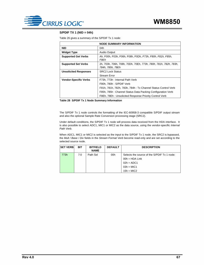
WM8850
Rev 4.0 67
S/PDIF TX 1 (NID = 04h)
Table 26 gives a summary of the S/PDIF Tx 1 node:
NODE SUMMARY INFORMATION
NID 04h
Widget Type Audio Output
Supported Get Verbs Ah, F00h, F03h, F06h, F08h, F0Dh, F73h, F80h, F81h, F85h,
F8Eh
Supported Set Verbs 2h, 703h, 706h, 708h, 70Dh, 70Eh, 773h, 780h, 781h, 782h, 783h,
784h, 785h, 78Eh
Unsolicited Responses SRC2 Lock Status
Stream Error
Vendor-Specific Verbs F73h, 773h : Internal Path Verb
F80h, 780h : S/PDIF Verb
F81h, 781h, 782h, 783h, 784h : Tx Channel Status Control Verb
F85h, 785h : Channel Status Data Packing Configuration Verb
F8Eh, 78Eh : Unsolicited Response Priority Control Verb
Table 28 S/PDIF Tx 1 Node Summary Information
The S/PDIF Tx 1 node controls the formatting of the IEC-60958-3 compatible S/PDIF output stream
and also the optional Sample Rate Conversion processing stage (SRC2).
Under default conditions, the S/PDIF Tx 1 node will process data received from the HDA interface. It
is also possible to select ADC1, MIC1 or MIC2 as the data source, using the vendor-specific Internal
Path Verb.
When ADC1, MIC1 or MIC2 is selected as the input to the S/PDIF Tx 1 node, the SRC2 is bypassed,
the Mult / Base / Div fields in the Stream Format Verb become read-only and are set according to the
selected source node.
SET VERB BIT BITFIELD
NAME
DEFAULT DESCRIPTION
773h 7:0 Path Sel 00h Selects the source of the S/PDIF Tx 1 node:
00h = HDA Link
02h = ADC1
03h = MIC1
15h = MIC2
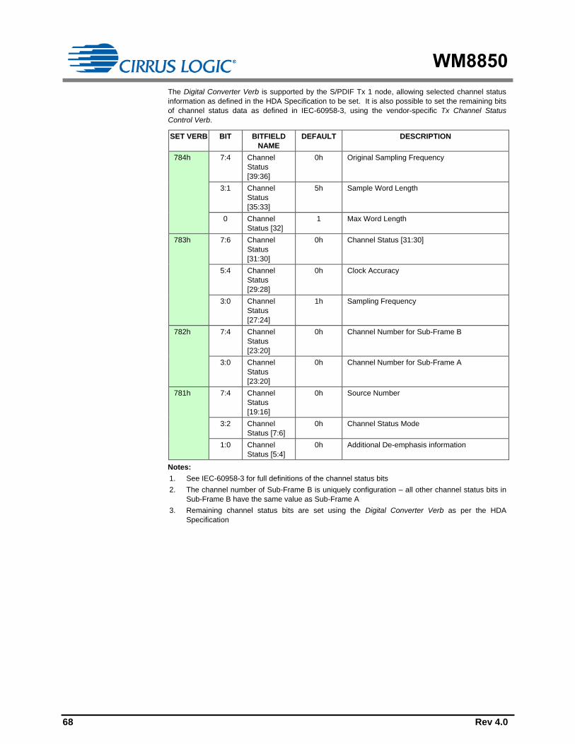
WM8850
68 Rev 4.0
The Digital Converter Verb is supported by the S/PDIF Tx 1 node, allowing selected channel status
information as defined in the HDA Specification to be set. It is also possible to set the remaining bits
of channel status data as defined in IEC-60958-3, using the vendor-specific Tx Channel Status
Control Verb.
SET VERB BIT BITFIELD
NAME
DEFAULT DESCRIPTION
784h 7:4 Channel
Status
[39:36]
0h Original Sampling Frequency
3:1 Channel
Status
[35:33]
5h Sample Word Length
0 Channel
Status [32]
1 Max Word Length
783h 7:6 Channel
Status
[31:30]
0h Channel Status [31:30]
5:4 Channel
Status
[29:28]
0h Clock Accuracy
3:0 Channel
Status
[27:24]
1h Sampling Frequency
782h 7:4 Channel
Status
[23:20]
0h Channel Number for Sub-Frame B
3:0 Channel
Status
[23:20]
0h Channel Number for Sub-Frame A
781h 7:4 Channel
Status
[19:16]
0h Source Number
3:2 Channel
Status [7:6]
0h Channel Status Mode
1:0 Channel
Status [5:4]
0h Additional De-emphasis information
Notes:
1. See IEC-60958-3 for full definitions of the channel status bits
2. The channel number of Sub-Frame B is uniquely configuration – all other channel status bits in
Sub-Frame B have the same value as Sub-Frame A
3. Remaining channel status bits are set using the Digital Converter Verb as per the HDA
Specification

WM8850
Rev 4.0 69
Under default conditions, the WM8850 will pack the S/PDIF Tx Channel Status Data with the correct
values of Sampling Frequency and Sample Word Length automatically, taking into account the
various routing options through the chip. This means the Channel Status Data always reflects the
same rate as the physical S/PDIF stream.
If required, this behaviour can be disabled using the vendor-specific Channel Status Data Packing
Configuration Verb. When CSD_MODE is set to 0, the S/PDIF Tx Channel Status Data is completely
defined using the vendor-specifc Tx Channel Status Control Verb.
SET VERB BIT BITFIELD
NAME
DEFAULT DESCRIPTION
785h 0 CSD_MODE 1 S/PDIF Transmitter Channel Status Data
Packing Mode:
0 = Manual mode: sample rate and data width
channel status data packed from data sourced
from the Tx Channel Status Control Verb
1 = Automatic mode: sample rate and data
width channel status data packed from data
sourced from the Stream Verb, S/PDIF Verb or
S/PDIF Rx Rate Detector (depending on
routing through device)
Note that the vendor-specific S/PDIF Verb supported by the S/PDIF Tx node is described in the
“S/PDIF Transmit using SRC2” section below.
S/PDIF OUT (NID = 0Fh)
Table 30 gives a summary of the S/PDIF Out node:
NODE SUMMARY INFORMATION
NID 0Fh
Widget Type Pin Complex
Supported Get Verbs F00h, F02h, F07h, F08h, F09h, F1Ch, F73h, F8Eh
Supported Set Verbs 707h, 708h, 71Ch, 71Dh, 71Eh, 71Fh, 773h, 78Eh
Unsolicited Responses Presence Detect
Vendor-Specific Verbs F73h, 773h : Internal Path Verb
F8Eh, 78Eh : Unsolicited Response Priority Control Verb
Table 29 S/PDIF Out Node Summary Information
The S/PDIF Out node controls the physical output to the SPDIFOUT1 pin.
Under default conditions, the S/PDIF Out node will output data from the S/PDIF Tx 1 node. It is also
possible to select S/PDIF In as the data source, using the vendor-specific Internal Path Verb.
SET VERB BIT BITFIELD
NAME
DEFAULT DESCRIPTION
773h 7:0 Path Sel 04h Selects the source of the S/PDIF Out node:
04h = S/PDIF Tx 1
10h = S/PDIF In
All other values of Path Sel are reserved.
Note: This verb will override the path indicated by the Get Connection List Entry Verb.

WM8850
70 Rev 4.0
S/PDIF TRANSMIT USING SRC2
The WM8850 provides a full-range sample rate converter, SRC2, to interface between the HDA link
domain and the S/PDIF transmitter (S/PDIF Tx 1) domain. SRC2 is implemented as a processing
function within the S/PDIF Tx 1 node, and so is enabled by the Processing State Verb as defined in
the HDA Specification.
When SRC2 is enabled, it is configured automatically by the WM8850, using the Stream Format Verb
for the input sample rate, and the vendor-specific S/PDIF Verb for the output. Figure 19 shows a
simplified diagram to demonstrate this:
S/PDIF Data
EncoderHDA Interface SRC2
S/PDIF
Output
SRC2 Output Sample RateSRC2 Input Sample Rate
Stream Format Verb S/PDIF Verb
Figure 19 S/PDIF Transmit using SRC2
Note that the SRC2 Sample Rate Converter is associated with the S/PDIF Tx 1 node only; there is no
SRC associated with S/PDIF Tx 2.
Note that, when SRC2 is enabled, the output S/PDIF stream will always contain 24-bit data.
The vendor-specific S/PDIF Verb implemented in the S/PDIF Tx 1 node is described below.
When SRC2 is enabled, the lock status is reported using the SRC_LOCK bit. When SRC2 is
unlocked, it will output zero samples at the rate programmed by the Stream Format Verb. When
SRC2 gains lock, transmission of valid samples will begin.
The LINKED_MODE bit provides the option to synchronise the S/PDIF Tx 1 output with the S/PDIF
Rx input stream. Further details of this function are provided below.
GET VERB BIT BITFIELD
NAME
DEFAULT DESCRIPTION
F80h 8 SRC_LOCK 0 SRC2 lock flag:
0 = SRC2 unlocked
1 = SRC2 locked
7 SRC_BASE 0 Used to set the base rate frequency:
0 = 48 kHz
1 = 44.1 kHz
6:4 SRC_MULT 0h Used to set the base rate multiplication factor:
0h = x1 (48 kHz, 44.1 kHz or less)
1h = x2 (96 kHz, 88.2 kHz, 32 kHz)
2h = Reserved
3h = x4 (192 kHz, 176.4 kHz)
4h-7h = Reserved
3:1 SRC_DIV 0h Used to set the base rate division factor:
0h = divide by 1 (48 kHz, 44.1 kHz)
1h = Reserved
2h = divide by 3 (32 kHz)
3h-7h= Reserved
0 LINKED_
MODE
0 Linked mode control:
0 = Linked mode disabled
1 – Linked mode enabled

WM8850
Rev 4.0 71
When the LINKED_MODE bit is set in the S/PDIF Verb, the S/PDIF Tx 1 output is synchronised to the
S/PDIF Rx input stream. In this mode, the SRC_BASE register field should be set to match the base
rate frequency of the Input Sample Rate. The SRC_MULT and SRC_DIV fields can be used to select
a range of S/PDIF Tx1 output sample rates which are synchronous to the received S/PDIF Rx sample
rate. Figure 20 shows a simplified diagram:
S/PDIF Data
EncoderHDA Interface SRC2
S/PDIF
Output
SRC2 Output Sample Rate (SRC_MULT, SRC_DIV)SRC2 Input Sample Rate
Stream Format Verb S/PDIF Verb
S/PDIF
FIFO and Rate
DetectorS/PDIF
Input
Sample Rate
SRC2 Output Sample Rate (SRC_BASE)
Figure 20 S/PDIF Transmit - Linked Mode
S/PDIF TRANSMIT WITHOUT USING SRC2
When SRC2 is not enabled, the output sample rate of the S/PDIF stream is controlled directly from
Stream Format Verb. Figure 21 shows a simplified diagram:
S/PDIF Data
EncoderHDA Interface
S/PDIF
Output
Output sample rate controlled by Stream Format Verb
Stream Format Verb
Figure 21 S/PDIF Transmit without SRC2

WM8850
72 Rev 4.0
S/PDIF TX 2 (NID = 17h)
Table 30 gives a summary of the S/PDIF Tx 2 node:
NODE SUMMARY INFORMATION
NID 17h
Widget Type Audio Output
Supported Get Verbs Ah, F00h, F06h, F08h, F0Dh, F73h, F81h, F85h, F8Eh
Supported Set Verbs 2h, 706h, 708h, 70Dh, 70Eh, 773h, 781h, 782h, 783h, 784h, 785h,
78Eh
Unsolicited Responses Stream Error
Vendor-Specific Verbs F73h, 773h : Internal Path Verb
F81h, 781h, 782h, 783h, 784h : Tx Channel Status Control Verb
F85h, 785h : Channel Status Data Packing Configuration Verb
F8Eh, 78Eh ; Unsolicited Response Priority Control Verb
Table 30 S/PDIF Tx 2 Node Summary Information
The S/PDIF Tx 2 node controls the formatting of the IEC-60958-3 compatible S/PDIF output stream.
Under default conditions, the S/PDIF Tx 2 node will process data received from the HDA interface. It
is also possible to select ADC1, MIC1 or MIC2 as the data source, using the vendor-specific Internal
Path Verb.
When ADC1, MIC1 or MIC2 is selected as the input to the S/PDIF Tx 2 node, the Mult / Base / Div
fields in the Stream Format Verb become read-only and are set according to the selected source
node.
SET VERB BIT BITFIELD
NAME
DEFAULT DESCRIPTION
773h 7:0 Path Sel 00h Selects the source of the S/PDIF Tx 2 node:
00h = HDA Link
02h = ADC1
03h = MIC1
15h = MIC2
The Digital Converter Verb is supported by the S/PDIF Tx 2 node, allowing selected channel status
information as defined in the HDA Specification to be set. It is also possible to set the remaining bits
of channel status data as defined in IEC-60958-3, using the vendor-specific Tx Channel Status
Control Verb.
SET VERB BIT BITFIELD
NAME
DEFAULT DESCRIPTION
784h 7:4 Channel
Status
[39:36]
0h Original Sampling Frequency
3:1 Channel
Status
[35:33]
5h Sample Word Length
0 Channel
Status [32]
1 Max Word Length
783h 7:6 Channel
Status
[31:30]
0h Channel Status [31:30]
5:4 Channel
Status
[29:28]
0h Clock Accuracy
3:0 Channel
Status
[27:24]
1h Sampling Frequency
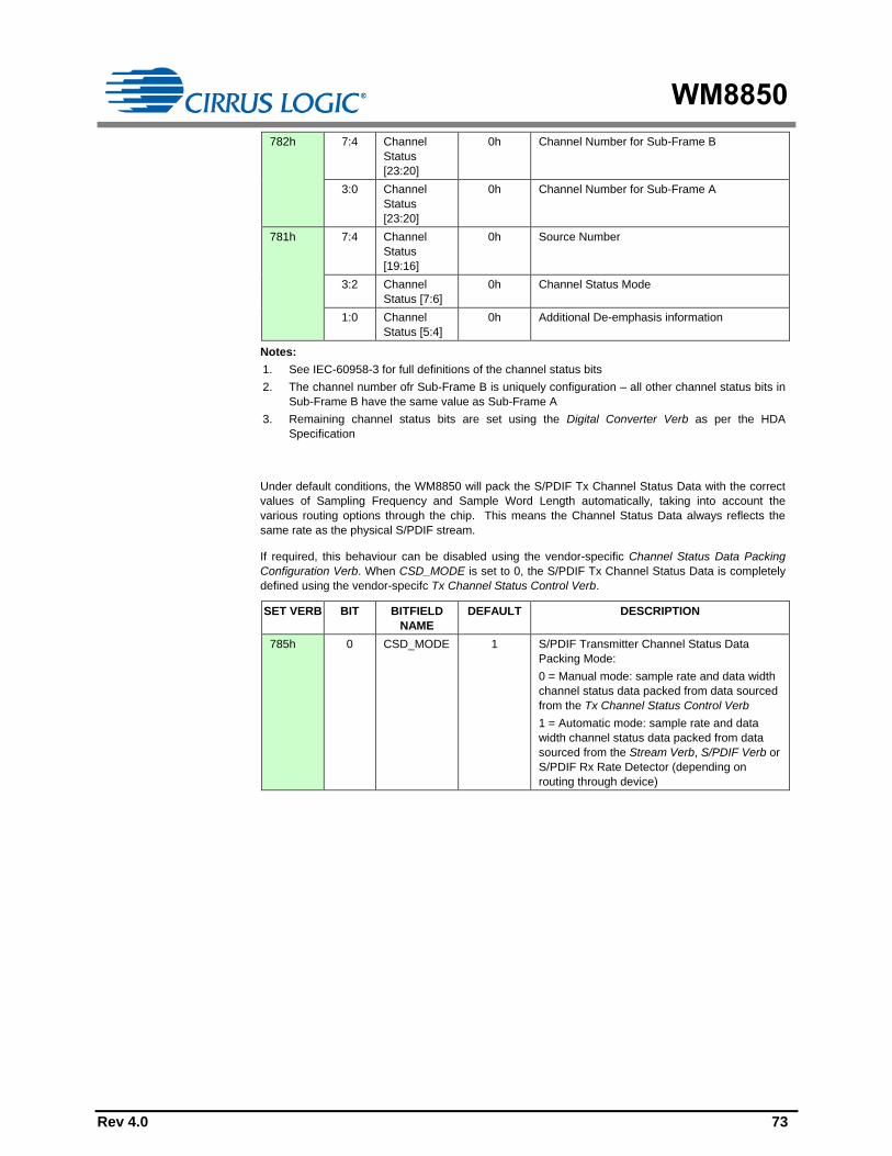
WM8850
Rev 4.0 73
782h 7:4 Channel
Status
[23:20]
0h Channel Number for Sub-Frame B
3:0 Channel
Status
[23:20]
0h Channel Number for Sub-Frame A
781h 7:4 Channel
Status
[19:16]
0h Source Number
3:2 Channel
Status [7:6]
0h Channel Status Mode
1:0 Channel
Status [5:4]
0h Additional De-emphasis information
Notes:
1. See IEC-60958-3 for full definitions of the channel status bits
2. The channel number ofr Sub-Frame B is uniquely configuration – all other channel status bits in
Sub-Frame B have the same value as Sub-Frame A
3. Remaining channel status bits are set using the Digital Converter Verb as per the HDA
Specification
Under default conditions, the WM8850 will pack the S/PDIF Tx Channel Status Data with the correct
values of Sampling Frequency and Sample Word Length automatically, taking into account the
various routing options through the chip. This means the Channel Status Data always reflects the
same rate as the physical S/PDIF stream.
If required, this behaviour can be disabled using the vendor-specific Channel Status Data Packing
Configuration Verb. When CSD_MODE is set to 0, the S/PDIF Tx Channel Status Data is completely
defined using the vendor-specifc Tx Channel Status Control Verb.
SET VERB BIT BITFIELD
NAME
DEFAULT DESCRIPTION
785h 0 CSD_MODE 1 S/PDIF Transmitter Channel Status Data
Packing Mode:
0 = Manual mode: sample rate and data width
channel status data packed from data sourced
from the Tx Channel Status Control Verb
1 = Automatic mode: sample rate and data
width channel status data packed from data
sourced from the Stream Verb, S/PDIF Verb or
S/PDIF Rx Rate Detector (depending on
routing through device)
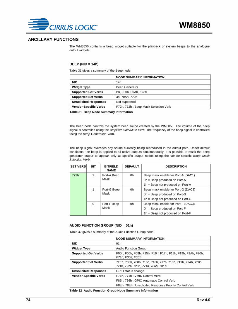
WM8850
74 Rev 4.0
ANCILLARY FUNCTIONS
The WM8850 contains a beep widget suitable for the playback of system beeps to the analogue
output widgets.
BEEP (NID = 14h)
Table 31 gives a summary of the Beep node:
NODE SUMMARY INFORMATION
NID 14h
Widget Type Beep Generator
Supported Get Verbs Bh, F00h, F0Ah, F72h
Supported Set Verbs 3h, 70Ah, 772h
Unsolicited Responses Not supported
Vendor-Specific Verbs F72h, 772h : Beep Mask Selection Verb
Table 31 Beep Node Summary Information
The Beep node controls the system beep sound created by the WM8850. The volume of the beep
signal is controlled using the Amplifier Gain/Mute Verb. The frequency of the beep signal is controlled
using the Beep Generation Verb.
The beep signal overrides any sound currently being reproduced in the output path. Under default
conditions, the beep is applied to all active outputs simultaneously. It is possible to mask the beep
generator output to appear only at specific output nodes using the vendor-specific Beep Mask
Selection Verb.
SET VERB BIT BITFIELD
NAME
DEFAULT DESCRIPTION
772h 2 Port-A Beep
Mask
0h Beep mask enable for Port-A (DAC1)
0h = Beep produced on Port-A
1h = Beep not produced on Port-A
1 Port-G Beep
Mask
0h Beep mask enable for Port-G (DAC2)
0h = Beep produced on Port-G
1h = Beep not produced on Port-G
0 Port-F Beep
Mask
0h Beep mask enable for Port-F (DAC3)
0h = Beep produced on Port-F
1h = Beep not produced on Port-F
AUDIO FUNCTION GROUP (NID = 01h)
Table 32 gives a summary of the Audio Function Group node:
NODE SUMMARY INFORMATION
NID 01h
Widget Type Audio Function Group
Supported Get Verbs F00h, F05h, F08h, F15h, F16h, F17h, F18h, F19h, F1Ah, F20h,
F71h, F86h, F8Eh
Supported Set Verbs 7FFh, 705h, 708h, 715h, 716h, 717h, 718h, 719h, 71Ah, 720h,
721h, 722h, 723h, 771h, 786h, 78Eh
Unsolicited Responses GPIO status change
Vendor-Specific Verbs F71h, 771h : VMID Control Verb
F86h, 786h : GPIO Automatic Control Verb
F8Eh, 78Eh : Unsolicited Response Priority Control Verb
Table 32 Audio Function Group Node Summary Information

WM8850
Rev 4.0 75
VMID Voltage Reference Control
The analogue circuits in the WM8850 require a mid-rail analogue reference voltage, VMID. This
reference is generated from AVDD via a programmable resistor chain. Together with the external
VMID decoupling capacitor, the programmable resistor chain determines the charging rate on VMID.
The resistor chain is selected using VMID_SEL, and can be used to optimise the reference for normal
operation, low power standby or for fast start-up.
The VMID charge rate is controlled by VMID_SEL and the external VMID capacitor. The VMID_RATE
field can be used to control the WM8850 power state according to the appropriate VMID conditions. In
start-up from power state D4, the WM8850 will not indicate the D3 power state until the time set by
VMID_RATE has elapsed.
The VMID_SEL and VMID_RATE fields are part of the VMID Control Verb.
SET VERB BIT BITFIELD
NAME
DEFAULT DESCRIPTION
771h 4:2 VMID_RATE 2h Time allocated to charge VMID:
0h = 1024ms
1h = 512ms
2h = 256ms
3h = 128ms
4h = 64ms
5h = 32ms
6h = 16ms
7h = 8ms
1:0 VMID_SEL 2h VMID String Source Impedance Select:
0h = 12.5k
1h = 75
2h = 37.5k
3h = 375k
Note: These figures give the value of the
resistor from AVDD to VMID and from VMID to
GND.
GPIO2 Automatic Control Mode
The GPIO Automatic Control Verb controls the behaviour of the GPIO2 pin.
In a system where external speaker amplifiers are connected to the WM8850 the GPIO2 pin may be
used to control the enable pin(s) of these amplifiers. For this application, it is possible to
automatically configure the GPIO2 pin as an output and to control its logic level as a function of the
AFG power state. This function is enabled by setting GPIO2_AUTO=1 in the vendor-specifc GPIO
Automatic Control Verb:
SET VERB BIT BITFIELD
NAME
DEFAULT DESCRIPTION
786h 0 GPIO2_
AUTO
1 GPIO2 Control Mode:
0 = GPIO2 Manual Mode
1 = GPIO Automatic Control Mode
The behaviour of GPIO2 when GPIO2_AUTO=1 is summarised in Table 33 below. When
GPIO2_AUTO=0 the behaviour of GPIO2 is as per the standard GPIO verbs.

WM8850
76 Rev 4.0
AFG PS-Act GPIO2 Output
0 Logic 1
1 Logic 1
2 Logic 0
3 Logic 0
4 Logic 0
Table 33 GPIO2 Automatic Control Mode Summary
Unsolicited Response Priority Control Verb
The Unsolicited Response Priority Control Verb is supported by multiple nodes within the WM8850,
including the Audio Function Group (AFG) node. This verb allows the Unsolicited Responses
associated with each node to be prioritised relative to the other nodes.
The priority level for each node is set using the Priority field within the Unsolicited Response Priority
Control Verb. When more than one Unsolicited Response is awaiting transmission, the node with the
lowest Priority is placed at the front of the queue. Nodes that have the same Priority setting are
queued on a ‘first to trigger’ basis.
Note that the lowest value of Priority represents the highest position in the queue.
The Unsolicited Response Priority Control Verb is defined as follows.
SET VERB BIT BITFIELD
NAME
DEFAULT DESCRIPTION
78Eh 4:0 Priority 00h Assigns a priority setting for queued
Unsolicited Responses. Nodes with the lowest
value have the highest priority, and so go to
the front of the Unsolicited Response queue.
Nodes with the same value for priority are
queued on first-to-trigger basis.
00h = Highest priority
…
1Fh = Lowest priority.

WM8850
Rev 4.0 77
UNSOLICITED RESPONSES
The High Definition Audio Specification provides support for software interrupts to be generated by
the CODEC independent of verb commands sent to the CODEC: these are known as Unsolicited
Responses. This section defines how the WM8850 creates Unsolicited Responses, explains some of
the novel features in the WM8850 to manage them, and what each Unsolicited Response from each
node represents. This section assumes familiarity with the High Definition Audio Specification.
GENERATING UNSOLICITED RESPONSES
Unsolicited Responses can only be sent wherever a null response would normally be sent.
Unsolicited Responses are queued on a frame-basis. That is, if an Unsolicited Response is issued in
the current frame, it is sent on the next frame containing a null response.
PRIORITY QUEUING
Where more than one Unsolicited Response is awaiting transmission, they are queued such that the
Unsolicited Response with the lowest Priority value (set using the Unsolicited Response Priority
Control Verb) is at the front of the queue. Nodes that have the same Priority setting are queued on a
‘first-to-trigger’ basis.
The Unsolicited Response Priority Control Verb is described in the “Ancillary Functions” section
describing the Audio Function Group node.
IN-QUEUE-UPDATE
The WM8850 stores all flags that trigger an Unsolicited Response. If a node triggers an Unsolicited
Response, the Unsolicited Response is queued as described above. Should the same node trigger a
second Unsolicited Response (from a different flag within that node) while the first is being queued,
the Unsolicited Response is updated to show both flags. This is known as an ‘In-Queue-Update’.
Should the same node trigger a second Unsolicited Response (from the same flag within the node)
while the first is being queued, only one Unsolicited Response is sent for both events.

WM8850
78 Rev 4.0
The concepts of Priority Queuing and In-Queue-Update are illustrated with the example in Figure 22.
[31:26] = 06h
[25:1] = 000000h
[0] = 1
(a)
(b)
(c)
(d)
Priority = 01
SAMPLE_DROP
0…… …… …...
1STREAM_ERR
Empty
Queue Slot
Empty
Queue Slot
Empty
Queue Slot
Priority = 01
0SAMPLE_DROP
0…… …… …...
1STREAM_ERR
Priority = 00
0
00GPIO2
01GPIO1
Priority = 01
0SAMPLE_DROP
0…… …… …...
1STREAM_ERR
Priority = 00
0
01GPIO2
01GPIO1
Priority = 01
0SAMPLE_DROP
0…… …… …...
1STREAM_ERR
Empty
Queue Slot
Priority = 01
0SAMPLE_DROP
0…… …… …...
1STREAM_ERR
Empty
Queue Slot
Empty
Queue Slot
Empty
Queue Slot
[31:26] = 01h
[25:4] = 000000h
[3:0] = 5h
[31:0] = 00000000h[31:0] = 00000000h[31:0] = 00000000h[31:0] = 00000000h[31:0] = 00000000h
STREAM_ERR
GPIO1
GPIO2
0
0
1
1
RESPONSE
Unsolicited
Response
Queue
front
back
(e)
(f)
6Tag
0
1Tag 1Tag 6Tag 6Tag
6Tag6Tag
…… …… …... …… …… …...
Figure 22 Priority Queuing and In-Queue Updates
a) STREAM_ERR flag asserts from DAC1 Node (NID = 06h), and an Unsolicited Response
(Tag ID = 06h) is queued awaiting a null response slot. STREAM_ERR rescinds at the end
of the HDA frame.
b) GPIO1 input changes to a 1 so the GPIO1 flag (from AFG NID = 01h) asserts and queues
an Unsolicited Response (Tag ID = 01h). This Unsolicited Response goes to the front of
the queue as its Priority value is lower (indicating higher priority) than the Priority setting of
the Unsolicited Response presently at the front of the queue.
c) GPIO2 input changes to a 1 so the GPIO2 flag asserts. The GPIO2_UPD flag is from the
AFG (NID = 01h), and as there is already an Unsolicited Response from this node in the
queue, the queued Unsolicited Response is updated to show both events (as highlighted
with the yellow box). This is known as an ‘In-Queue-Update’.
d) A slot becomes available for sending an Unsolicited Response, so the AFG Unsolicited
Response is transmitted as it is at the front of the queue.
e) STREAM_ERR asserts from DAC1 Node (NID = 06h). As there is already an Unsolicited
Response in the queue from this node, the Unsolicited Response is simply updated (as
shown in the purple box). However, the queued Unsolicited Response already shows that
there has been a STREAM_ERR flag so the In-Queue-Update does not actually change the
Unsolicited Response value.
f) A slot becomes available for sending an Unsolicited Response, so the Unsolicited
Response (Tag ID = 06h) is transmitted.

WM8850
Rev 4.0 79
UNSOLICITED RESPONSE TYPES
There are three types of flags that are returned by the WM8850, prefixed in the register map as
follows:
SF = UNSOLICITED RESPONSE STATUS FLAG
Unsolicited Response Status Flags (SF) are used to indicate that there has been a change in flag
state, and (where possible) convey what the new state is. A change in state is typically something
that will persist for a number of HDA frames. A state change will trigger an Unsolicited Response, but
it is possible that a state change can occur more than once while an Unsolicited Response is being
queued.
To indicate this, Unsolicited Response Status Flags are 2-bits wide and are encoded as follows:
0h = Flag did not trigger Unsolicited Response.
1h = Rising edge of flag triggered Unsolicited Response.
2h = Falling edge of flag triggered Unsolicited Response.
3h = Rising and falling edges of the flag have been detected while the Unsolicited Response has
been queued
When the Unsolicited Response Status Flag is reported as 0h, the user is informed that there has
been no change in status. When the Unsolicited Response Status Flag is reported as 1h or 2h, the
user is informed that there has been a change in status and what the new status value is. When the
Unsolicited Response Status Flag is reported as 3h, the user is informed of a multiple change in
status, and the user should read the associated flag’s status register to get the current status value of
the flag.
UF = UNSOLICITED RESPONSE UPDATE FLAG
Unsolicited Response Update Flags (UF) are used to indicate that there has been one or more
changes to the value of some status registers. The status register should be read (through the issue
of the appropriate Get command), to see the current register value.
EF = UNSOLICITED RESPONSE EVENT FLAG
Unsolicited Response Event Flags (EF) are used to indicate that an event has occurred during an
HDA Frame. The occurrence of an event will trigger an Unsolicited Response.

WM8850
80 Rev 4.0
UNSOLICITED RESPONSE DEFINITIONS
Table 34 gives a summary of the definitions of the Unsolicited Responses from each node in the
WM8850. Note that these responses are generated only when the node is set to generate them,
using the Unsolicited Reponse Verb as defined in the HDA specification.
NID NODE
NAME
UNSOLICITED RESPONSE
BIT FLAG NAME DESCRIPTION
01h AFG [31:26] Tag A software programmable tag value. The default value is equal to
the Node ID. Other values can be configured using the Unsolicited
Response Verb.
[25:4] Rsvd Reserved
[3:2] SF_GPIO2 Indicates that the value on GPIO2 (configured as an input) has
changed, and reports new status value.
When the AFG is in power state D0, D1 or D2, a change in GPIO
status triggers an Unsolicited Response.
When the AFG is in power state D3, a change in GPIO status
triggers a power state change request.
Note that the status value is also accessible through the Get GPIO
Data Verb.
[1:0] SF_GPIO1 Indicates that the value on GPIO1 (configured as an input) has
changed, and reports new status value.
When the AFG is in power state D0, D1 or D2, a change in GPIO
status triggers an Unsolicited Response.
When the AFG is in power state D3, a change in GPIO status
triggers a power state change request.
Note that the status value is also accessible through the Get GPIO
Data Verb.
02h ADC1 [31:26] Tag A software programmable tag value. The default value is equal to
the Node ID. Other values can be configured using the Unsolicited
Response Verb.
[25:1] Rsvd Reserved
[0] EF_STREAM_DROP Indicates that the stream associated with the ADC1 node has been
dropped due to the bandwidth of the SDI line being
oversubscribed.
Assertion of the flag triggers an Unsolicited Response.
The flag is cleared when the Stream ID is written to.
03h MIC1 [31:26] Tag A software programmable tag value. The default value is equal to
the Node ID. Other values can be configured using the Unsolicited
Response Verb.
[25:1] Rsvd Reserved
[0] EF_STREAM_DROP Indicates that the stream associated with the MIC1 node has been
dropped due to the bandwidth of the SDI line being
oversubscribed.
Assertion of the flag triggers an Unsolicited Response.
The flag is cleared when the Stream ID is written to.
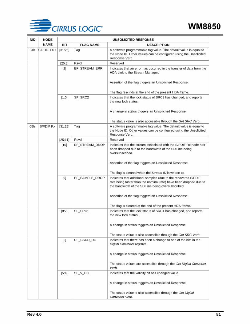
WM8850
Rev 4.0 81
NID NODE
NAME
UNSOLICITED RESPONSE
BIT FLAG NAME DESCRIPTION
04h S/PDIF TX 1 [31:26] Tag A software programmable tag value. The default value is equal to
the Node ID. Other values can be configured using the Unsolicited
Response Verb.
[25:3] Rsvd Reserved
[2] EF_STREAM_ERR Indicates that an error has occurred in the transfer of data from the
HDA Link to the Stream Manager.
Assertion of the flag triggers an Unsolicited Response.
The flag rescinds at the end of the present HDA frame.
[1:0] SF_SRC2 Indicates that the lock status of SRC2 has changed, and reports
the new lock status.
A change in status triggers an Unsolicited Response.
The status value is also accessible through the Get SRC Verb.
05h S/PDIF Rx [31:26] Tag A software programmable tag value. The default value is equal to
the Node ID. Other values can be configured using the Unsolicited
Response Verb.
[25:11] Rsvd Reserved
[10] EF_STREAM_DROP Indicates that the stream associated with the S/PDIF Rx node has
been dropped due to the bandwidth of the SDI line being
oversubscribed.
Assertion of the flag triggers an Unsolicited Response.
The flag is cleared when the Stream ID is written to.
[9] EF_SAMPLE_DROP Indicates that additional samples (due to the recovered S/PDIF
rate being faster than the nominal rate) have been dropped due to
the bandwidth of the SDI line being oversubscribed.
Assertion of the flag triggers an Unsolicited Response.
The flag is cleared at the end of the present HDA frame.
[8:7] SF_SRC1 Indicates that the lock status of SRC1 has changed, and reports
the new lock status.
A change in status triggers an Unsolicited Response.
The status value is also accessible through the Get SRC Verb.
[6] UF_CSUD_DC Indicates that there has been a change to one of the bits in the
Digital Converter register.
A change in status triggers an Unsolicited Response.
The status values are accessible through the Get Digital Converter
Verb.
[5:4] SF_V_DC Indicates that the validity bit has changed value.
A change in status triggers an Unsolicited Response.
The status value is also accessible through the Get Digital
Converter Verb.

WM8850
82 Rev 4.0
NID NODE
NAME
UNSOLICITED RESPONSE
BIT FLAG NAME DESCRIPTION
[3] UF_CSUD_CON Indicates that one (or more) of the first 40-bits of the channel
status frame has changed.
A change in status triggers an Unsolicited Response.
The status values are accessible through the Get Channel Status
Verb.
[2:1] SF_NAF Indicates that the non-audio flag (defined in IEC-61937) has
changed value.
A change in status triggers an Unsolicited Response.
The status value is also accessible through the Get Non-Audio
Flag Verb.
[0] EF_DATA_ERR Indicates there has been a parity error, bi-phase encoding error or
that preambles have been recovered out of sequence in the
received S/PDIF stream.
Assertion of the flag triggers an Unsolicited Response.
The flag is cleared at the end of the present HDA frame.
06h DAC1 [31:26] Tag A software programmable tag value. The default value is equal to
the Node ID. Other values can be configured using the Unsolicited
Response Verb.
[25:1] Rsvd Reserved
[0] EF_STREAM_ERR Indicates that an error has occurred in the transfer of data from the
HDA Link to the Stream Manager.
Assertion of the flag triggers an Unsolicited Response.
The flag is cleared at the end of the present HDA frame.
07h DAC2 [31:26] Tag A software programmable tag value. The default value is equal to
the Node ID. Other values can be configured using the Unsolicited
Response Verb.
[25:1] Rsvd Reserved
[0] EF_STREAM_ERR Indicates that an error has occurred in the transfer of data from the
HDA Link to the Stream Manager.
Assertion of the flag triggers an Unsolicited Response.
The flag is cleared at the end of the present HDA frame.
08h DAC3 [31:26] Tag A software programmable tag value. The default value is equal to
the Node ID. Other values can be configured using the Unsolicited
Response Verb.
[25:1] Rsvd Reserved
[0] EF_STREAM_ERR Indicates that an error has occurred in the transfer of data from the
HDA Link to the Stream Manager.
Assertion of the flag triggers an Unsolicited Response.
The flag is cleared at the end of the present HDA frame.

WM8850
Rev 4.0 83
NID NODE
NAME
UNSOLICITED RESPONSE
BIT FLAG NAME DESCRIPTION
0Ch Port-E [31:26] Tag A software programmable tag value. The default value is equal to
the Node ID. Other values can be configured using the Unsolicited
Response Verb.
[25:2] Rsvd Reserved
[1:0] SF_PD Indicates that the Presence Detect value (in the Pin Sense Verb)
has changed.
A change in status triggers an Unsolicited Response (when the
AFG is in power state D0, D1, D2) or it triggers a power state
change request (when the AFG is in power state D3).
The status value is also accessible through the Get Pin Sense
Verb.
0Dh Port-B [31:26] Tag A software programmable tag value. The default value is equal to
the Node ID. Other values can be configured using the Unsolicited
Response Verb.
[25:3] Rsvd Reserved
[2] EF_IMP Indicates that the Impedance Sense value is ready.
Assertion of the flag triggers an Unsolicited Response.
The flag is cleared on an issue of a Get Pin Sense Verb.
[1:0] SF_PD Indicates that the Presence Detect value (in the Pin Sense Verb)
has changed.
A change in status triggers an Unsolicited Response (when the
AFG is in power state D0, D1, D2) or it triggers a power state
change request (when the AFG is in power state D3).
The status value is also accessible through the Get Pin Sense
Verb.
0Fh S/PDIF Out [31:26] Tag A software programmable tag value. The default value is equal to
the Node ID. Other values can be configured using the Unsolicited
Response Verb.
[25:2] Rsvd Reserved
[1:0] SF_PD Indicates that the Presence Detect value (in the Pin Sense Verb)
has changed.
A change in status triggers an Unsolicited Response (when the
AFG is in power state D0, D1, D2) or it triggers a power state
change request (when the AFG is in power state D3).
The status value is also accessible through the Get Pin Sense
Verb.

WM8850
84 Rev 4.0
NID NODE
NAME
UNSOLICITED RESPONSE
BIT FLAG NAME DESCRIPTION
10h S/PDIF In [31:26] Tag A software programmable tag value. The default value is equal to
the Node ID. Other values can be configured using the Unsolicited
Response Verb.
[25:5] Rsvd Reserved
[4] UF_RATE Indicates that the recovered sample rate of the S/PDIF receiver
has changed.
A change in status triggers an Unsolicited Response.
The status value is accessible through the Get S/PDIF In Status
Verb.
[3:2] SF_SPDIN Indicates that the Lock status of the in the S/PDIF Receiver.
A change in status triggers an Unsolicited Response.
The status value is also accessible through the Get S/PDIF In
Status Verb.
[1:0] SF_PD Indicates that the Presence Detect value (in the Pin Sense Verb)
has changed.
A change in status triggers an Unsolicited Response (when the
AFG is in power state D0, D1, D2) or it triggers a power state
change request (when the AFG is in power state D3).
The status value is also accessible through the Get Pin Sense
Verb.
11h Port-A [31:26] Tag A software programmable tag value. The default value is equal to
the Node ID. Other values can be configured using the Unsolicited
Response Verb.
[25:2] Rsvd Reserved
[1:0] SF_PD Indicates that the Presence Detect value (in the Pin Sense Verb)
has changed.
A change in status triggers an Unsolicited Response (when the
AFG is in power state D0, D1, D2) or it triggers a power state
change request (when the AFG is in power state D3).
The status value is also accessible through the Get Pin Sense
Verb.
12h Port-G [31:26] Tag A software programmable tag value. The default value is equal to
the Node ID. Other values can be configured using the Unsolicited
Response Verb.
[25:2] Rsvd Reserved
[1:0] SF_PD Indicates that the Presence Detect value (in the Pin Sense Verb)
has changed.
A change in status triggers an Unsolicited Response (when the
AFG is in power state D0, D1, D2) or it triggers a power state
change request (when the AFG is in power state D3).
The status value is also accessible through the Get Pin Sense
Verb.

WM8850
Rev 4.0 85
NID NODE
NAME
UNSOLICITED RESPONSE
BIT FLAG NAME DESCRIPTION
13h Port-F [31:26] Tag A software programmable tag value. The default value is equal to
the Node ID. Other values can be configured using the Unsolicited
Response Verb.
[25:2] Rsvd Reserved
[1:0] SF_PD Indicates that the Presence Detect value (in the Pin Sense Verb)
has changed.
A change in status triggers an Unsolicited Response (when the
AFG is in power state D0, D1, D2) or it triggers a power state
change request (when the AFG is in power state D3).
The status value is also accessible through the Get Pin Sense
Verb.
15h MIC2 [31:26] Tag A software programmable tag value. The default value is equal to
the Node ID. Other values can be configured using the Unsolicited
Response Verb.
[25:1] Rsvd Reserved
[0] EF_STREAM_DROP Indicates that the stream associated with the MIC2 node has been
dropped due to the bandwidth of the SDI line being
oversubscribed.
Assertion of the flag triggers an Unsolicited Response.
The flag is cleared when the Stream ID is written to.
17h S/PDIF Tx 2 [31:26] Tag A software programmable tag value. The default value is equal to
the Node ID. Other values can be configured using the Unsolicited
Response Verb.
[25:1] Rsvd Reserved
[0] EF_STREAM_ERR Indicates that an error has occurred in the transfer of data from the
HDA Link to the Stream Manager.
Assertion of the flag triggers an Unsolicited Response.
The flag is cleared at the end of the present HDA frame.
Table 34 Unsolicited Response Summary

WM8850
86 Rev 4.0

WM8850
Rev 4.0 87
00h
01h
02h
03h
04h
05h
06h
07h
08h
09h
0Ah
0Bh
0Ch
0Dh
0Eh
0Fh
10h
11h
12h
13h
14h
15h
16h
17h
DETAILED VERB DESCRIPTIONS
This section provides full verb information on each node in the WM8850. For verbs defined as part of
the High Definition Audio Specification Revision 1.0 this is the only information provided. For vendor-
specific verbs, more detailed explanation of the function is provided in the main text of the datasheet
above.
ROOT NODE (NID = 00H)
Verb ID Payload [7:0] Response[31:0]
Get F00h Parameter ID (PID) Parameter Value
Vendor ID Response Format (PID = 00h)
Bit Bitfield Name RW Default Description
[31:16] Vendor ID R 1AECh Vendor ID
[15:0] Device ID R 8800h Device ID = WM8800
Revision ID Response Format (PID = 02h)
Bit Bitfield Name RW Default Description
[31:24] Rsvd R 00h Reserved
[23:20] MajRev R 1h Major revision number (left of the decimal) of the HDA Specification to
which the WM8850 is fully compliant
[19:16] MinRev R 0h Minor revision number (right of the decimal) of the HDA Specification to
which the WM8850 is fully compliant
[15:8] Revision ID R - Cirrus Logic revision number for this device
[7:0] Stepping ID R - Optional stepping number within the Revision ID
Subordinate Node Count Response Format (PID = 04h)
Bit Bitfield Name RW Default Description
[31:24] Rsvd R 00h Reserved
[23:16] Starting NID R 01h Starting NID of the first function group
[15:8] Rsvd R 00h Reserved
[7:0] Total Nodes R 1h Total number of function group nodes

WM8850
88 Rev 4.0

WM8850
Rev 4.0 89
00h
01h
02h
03h
04h
05h
06h
07h
08h
09h
0Ah
0Bh
0Ch
0Dh
0Eh
0Fh
10h
11h
12h
13h
14h
15h
16h
17h
AUDIO FUNCTION GROUP (NID = 01H)
FUNCTION RESET VERB
Verb ID Payload [7:0] Response[31:0]
Execute 7FFh 00h 00000000h
Bit Bitfield Name RW Default Description
[7:0] Reset W 00h AFG reset.
00h = AFG and all widget nodes associated with the AFG will reset to
default values. The WM8850 will issue a response and then be ready to
accept commands in the frame following the valid response.
Note: The Implementation ID/Subsystem ID Verb and the Configuration
Default Verb will not be reset using this verb.
GET PARAMETER VERB
Verb ID Payload [7:0] Response[31:0]
Get F00h Parameter ID (PID) Parameter Value
Subordinate Node Count Response Format (PID = 04h)
Bit Bitfield Name RW Default Description
[31:24] Rsvd R 00h Reserved
[23:16] Starting NID R 02h Starting NID of the first widget in the AFG
[15:8] Rsvd R 00h Reserved
[7:0] Total Nodes R 16h Total number of widget nodes within the AFG
Function Group Type Response Format (PID = 05h)
Bit Bitfield Name RW Default Description
[31:9] Rsvd R 000000h Reserved
[8] Unsol R 1 The AFG Node is capable of generating Unsolicited Responses
[7:0] Node Type R 01h Node Type is Audio Function Group
Audio Function Group Capabilities Response Format (PID = 08h)
Bit Bitfield Name RW Default Description
[31:17] Rsvd R 0000h Reserved
[16] Beep Gen R 1 Beep Generator Widget present
[15:12] Rsvd R 00h Reserved
[11:8] Input Delay R 8h Number of samples of input delay
[7:4] Rsvd R 00h Reserved
[3:0] Output Delay R 8h Number of samples of output delay
Input Amplifier Capabilities Response Format (PID = 0Dh)
Bit Bitfield Name RW Default Description
[31] Mute Capable R 0 Microphone preamplifers are not capable of muting
[30:23] Rsvd R 00h Reserved
[22:16] Step Size R 27h Gain step size is 10dB
[15] Rsvd R 0 Reserved
[14:8] Num Steps R 03h Number of steps in gain range is 4 (0dB to +30dB)
[7] Rsvd R 0 Reserved
[6:0] Offset R 0h The step number that 0dB corresponds to is 0
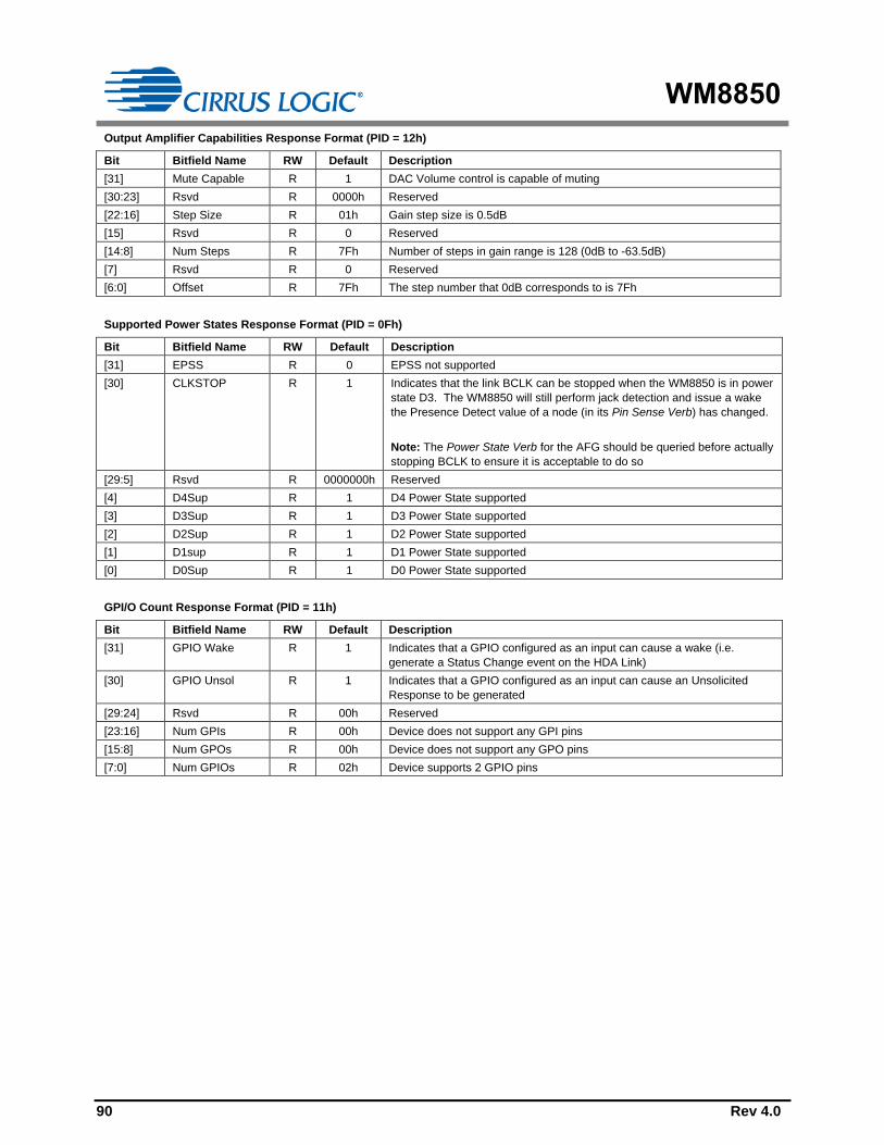
WM8850
90 Rev 4.0
Output Amplifier Capabilities Response Format (PID = 12h)
Bit Bitfield Name RW Default Description
[31] Mute Capable R 1 DAC Volume control is capable of muting
[30:23] Rsvd R 0000h Reserved
[22:16] Step Size R 01h Gain step size is 0.5dB
[15] Rsvd R 0 Reserved
[14:8] Num Steps R 7Fh Number of steps in gain range is 128 (0dB to -63.5dB)
[7] Rsvd R 0 Reserved
[6:0] Offset R 7Fh The step number that 0dB corresponds to is 7Fh
Supported Power States Response Format (PID = 0Fh)
Bit Bitfield Name RW Default Description
[31] EPSS R 0 EPSS not supported
[30] CLKSTOP R 1 Indicates that the link BCLK can be stopped when the WM8850 is in power
state D3. The WM8850 will still perform jack detection and issue a wake
the Presence Detect value of a node (in its Pin Sense Verb) has changed.
Note: The Power State Verb for the AFG should be queried before actually
stopping BCLK to ensure it is acceptable to do so
[29:5] Rsvd R 0000000h Reserved
[4] D4Sup R 1 D4 Power State supported
[3] D3Sup R 1 D3 Power State supported
[2] D2Sup R 1 D2 Power State supported
[1] D1sup R 1 D1 Power State supported
[0] D0Sup R 1 D0 Power State supported
GPI/O Count Response Format (PID = 11h)
Bit Bitfield Name RW Default Description
[31] GPIO Wake R 1 Indicates that a GPIO configured as an input can cause a wake (i.e.
generate a Status Change event on the HDA Link)
[30] GPIO Unsol R 1 Indicates that a GPIO configured as an input can cause an Unsolicited
Response to be generated
[29:24] Rsvd R 00h Reserved
[23:16] Num GPIs R 00h Device does not support any GPI pins
[15:8] Num GPOs R 00h Device does not support any GPO pins
[7:0] Num GPIOs R 02h Device supports 2 GPIO pins

WM8850
Rev 4.0 91
00h
01h
02h
03h
04h
05h
06h
07h
08h
09h
0Ah
0Bh
0Ch
0Dh
0Eh
0Fh
10h
11h
12h
13h
14h
15h
16h
17h
POWER STATE VERB
Verb ID Payload [7:0] Response[31:0]
Get F05h 00h Bits [31:0] in the table below
Set 705h Bits [7:0] in the table below 00000000h
Bit Bitfield Name RW Default Description
[31:10] Rsvd R 000000h Reserved
[9] PS-ClkStopOK R 0 Applicable when the AFG is in power state D3:
0 = BCLK must be kept running
1 = It is OK to stop BCLK
[8] Rsvd R 0 Reserved
[7:4] PS-Act R 2h Indicates the actual power state of the AFG node:
0h = D0
1h = D1
2h = D2
3h = D3
4h = D4
The power state of the AFG is controlled by PS-Set below. For the AFG,
PS-Act will equal PS-Set (offset by the time required to execute a power
state transition).
[3:0] PS-Set RW 2h Sets the power state of the AFG node:
0h = D0
1h = D1
2h = D2
3h = D3
4h = D4
Note: If the Link is operational, but the AFG is in power state D4, only Get Commands, Set Power State or AFG Reset
commands are executed – all other commands are ignored. In this scenario, the SDI line is inactive and does not transmit
responses, tags or data.
UNSOLICITED RESPONSE VERB
Verb ID Payload [7:0] Response[31:0]
Get F08h 00h Bits [31:0] in the table below
Set 708h Bits [7:0] in the table below 00000000h
Bit Bitfield Name RW Default Description
[31:8] Rsvd R 000000h Reserved
[7] Enable RW 0 0 = Unsolicited Responses disabled for this node
1 = Unsolicited Responses enabled for this node
[6] Rsvd R 0 Reserved
[5:0] Tag RW 01h A software programmable tag value that is returned in the top six bits
(31:26) of every Unsolicited Response from this node.
The default for Tag is equal to the Node ID.
Note: The Unsolicited Response for the AFG node is defined in the “Unsolicited Responses” section.
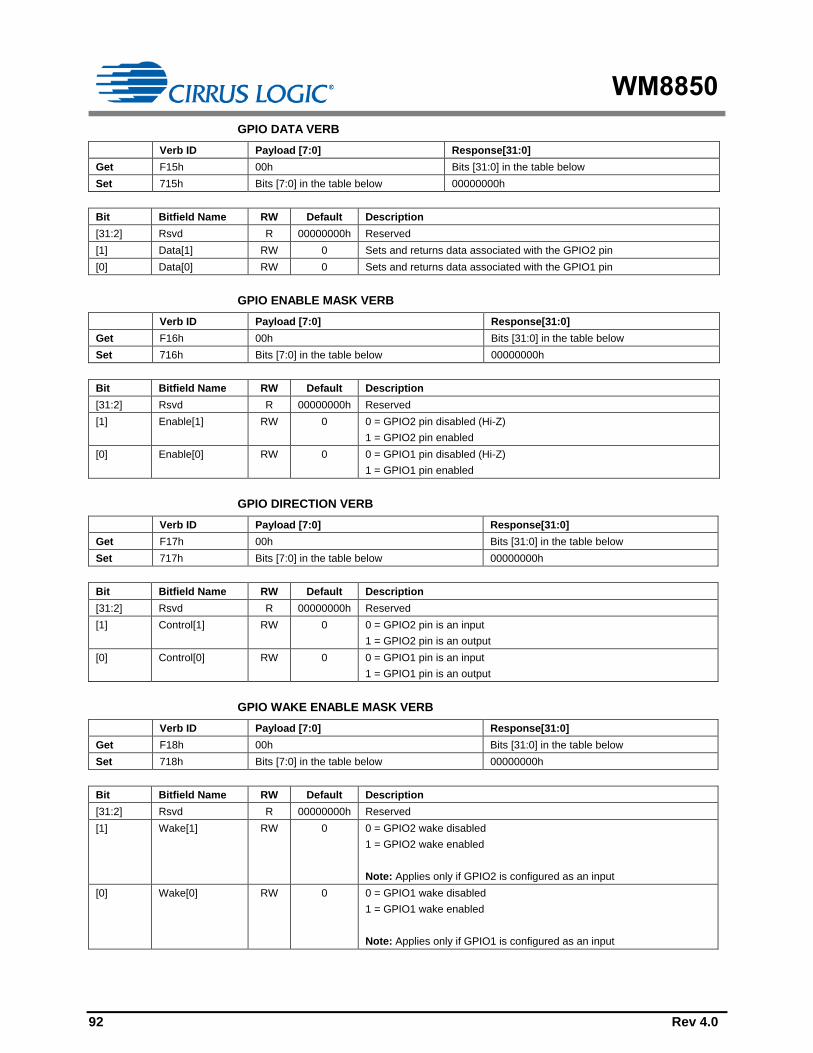
WM8850
92 Rev 4.0
GPIO DATA VERB
Verb ID Payload [7:0] Response[31:0]
Get F15h 00h Bits [31:0] in the table below
Set 715h Bits [7:0] in the table below 00000000h
Bit Bitfield Name RW Default Description
[31:2] Rsvd R 00000000h Reserved
[1] Data[1] RW 0 Sets and returns data associated with the GPIO2 pin
[0] Data[0] RW 0 Sets and returns data associated with the GPIO1 pin
GPIO ENABLE MASK VERB
Verb ID Payload [7:0] Response[31:0]
Get F16h 00h Bits [31:0] in the table below
Set 716h Bits [7:0] in the table below 00000000h
Bit Bitfield Name RW Default Description
[31:2] Rsvd R 00000000h Reserved
[1] Enable[1] RW 0 0 = GPIO2 pin disabled (Hi-Z)
1 = GPIO2 pin enabled
[0] Enable[0] RW 0 0 = GPIO1 pin disabled (Hi-Z)
1 = GPIO1 pin enabled
GPIO DIRECTION VERB
Verb ID Payload [7:0] Response[31:0]
Get F17h 00h Bits [31:0] in the table below
Set 717h Bits [7:0] in the table below 00000000h
Bit Bitfield Name RW Default Description
[31:2] Rsvd R 00000000h Reserved
[1] Control[1] RW 0 0 = GPIO2 pin is an input
1 = GPIO2 pin is an output
[0] Control[0] RW 0 0 = GPIO1 pin is an input
1 = GPIO1 pin is an output
GPIO WAKE ENABLE MASK VERB
Verb ID Payload [7:0] Response[31:0]
Get F18h 00h Bits [31:0] in the table below
Set 718h Bits [7:0] in the table below 00000000h
Bit Bitfield Name RW Default Description
[31:2] Rsvd R 00000000h Reserved
[1] Wake[1] RW 0 0 = GPIO2 wake disabled
1 = GPIO2 wake enabled
Note: Applies only if GPIO2 is configured as an input
[0] Wake[0] RW 0 0 = GPIO1 wake disabled
1 = GPIO1 wake enabled
Note: Applies only if GPIO1 is configured as an input

WM8850
Rev 4.0 93
00h
01h
02h
03h
04h
05h
06h
07h
08h
09h
0Ah
0Bh
0Ch
0Dh
0Eh
0Fh
10h
11h
12h
13h
14h
15h
16h
17h
GPIO UNSOLICITED ENABLE MASK VERB
Verb ID Payload [7:0] Response[31:0]
Get F19h 00h Bits [31:0] in the table below
Set 719h Bits [7:0] in the table below 00000000h
Bit Bitfield Name RW Default Description
[31:2] Rsvd R 00000000h Reserved
[1] UnsolEnable[1] RW 0 0 = GPIO2 cannot generate an Unsolicited Response
1 = GPIO2 can generate an Unsolicited Response
Note: Applies only if GPIO2 is configured as an input
[0] UnsolEnable[0] RW 0 0 = GPIO1 cannot generate an Unsolicited Response
1 = GPIO1 can generate an Unsolicited Response
Note: Applies only if GPIO1 is configured as an input
GPIO STICKY MASK VERB
Verb ID Payload [7:0] Response[31:0]
Get F1Ah 00h Bits [31:0] in the table below
Set 71Ah Bits [7:0] in the table below 00000000h
Bit Bitfield Name RW Default Description
[31:2] Rsvd R 00000000h Reserved
[1] Data[1] RW 0 0 = GPIO2 is non-sticky (level sensitive)
1 = GPIO2 is sticky (edge-sensitive)
Note: Applies only if GPIO2 is configured as an input
[0] Data[0] RW 0 0 = GPIO1 is non-sticky (level sensitive)
1 = GPIO1 is sticky (edge-sensitive)
Note: Applies only if GPIO1 is configured as an input
IMPLEMENTATION ID / SUBSYSTEM ID VERB
Verb ID Payload [7:0] Response[31:0]
Get F20h 00h Bits [31:0] in the table below
Set1 720h Implementation ID[7:0] 00h
Set2 721h Implementation ID[15:8] 00h
Set3 722h Implementation ID[23:16] 00h
Set4 723h Implementation ID[31:24] 00h
Bit Bitfield Name RW Default Description
[31:0] Implementation
ID
RW 00000100h Implementation ID
Note: The Implementation ID / Subsystem ID Verb is not reset to its default value during a reset from any source. The settings
are only lost when digital power is removed from the WM8850. When digital power is restored, the System BIOS must restore
the settings.

WM8850
94 Rev 4.0
VMID CONTROL VERB (VENDOR SPECIFIC)
Verb ID Payload [7:0] Response[31:0]
Get F71h 00h Bits [31:0] in the table below
Set 771h Bits [7:0] in the table below 00000000h
Bit Bitfield Name RW Default Description
[31:6] Rsvd R 0000000h Reserved
[4:2] VMID_RATE RW 2h Time allocated to charge VMID:
0h = 1024ms
1h = 512ms
2h = 256ms
3h = 128ms
4h = 64ms
5h = 32ms
6h = 16ms
7h = 8ms
[1:0] VMID_SEL RW 2h VMID String Source Impedance Select:
0h = 12.5k
1h = 75k
2h = 37.5k
3h = 375k
Note: These figures give the value of the resistor from AVDD to VMID
and from VMID to GND.
GPIO AUTOMATIC CONTROL VERB (VENDOR-SPECIFIC)
Verb ID Payload [7:0] Response[31:0]
Get F86h 00h Bits [31:0] in the table below
Set 786h Bits [7:0] in the table below 00000000h
Bit Bitfield Name RW Default Description
[31:1] Rsvd R 0000000h Reserved
[0] GPIO2_AUTO RW 1 GPIO2 Control Mode:
0 = GPIO2 Manual Mode
GPIO2 is controlled manually via the standard AFG verbs
1 = GPIO Automatic Control Mode
GPIO2 is always an output and forced high when PS-Act of AFG is D1 or
D0. GPIO2 is forced low when PS-Act of AFG is D2, D3 or D4.

WM8850
Rev 4.0 95
00h
01h
02h
03h
04h
05h
06h
07h
08h
09h
0Ah
0Bh
0Ch
0Dh
0Eh
0Fh
10h
11h
12h
13h
14h
15h
16h
17h
UNSOLICITED RESPONSE PRIORITY CONTROL VERB (VENDOR-SPECIFIC)
Verb ID Payload [7:0] Response[31:0]
Get F8Eh 00h Bits [31:0] in the table below
Set 78Eh Bits [7:0] in the table below 00000000h
Bit Bitfield Name RW Default Description
[31:5] Rsvd R 0000000h Reserved
[4:0] Priority RW 00h Assigns a priority setting for queued Unsolicited Responses. Nodes with
the lowest value have the highest priority, and so go to the front of the
Unsolicited Response queue. Nodes with the same value for priority are
queued on first-to-trigger basis.
00h = Highest priority
…
1Fh = Lowest priority.

WM8850
96 Rev 4.0
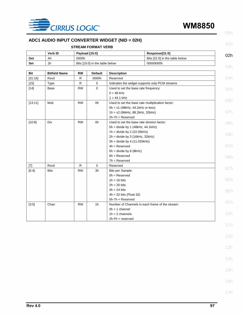
WM8850
Rev 4.0 97
00h
01h
02h
03h
04h
05h
06h
07h
08h
09h
0Ah
0Bh
0Ch
0Dh
0Eh
0Fh
10h
11h
12h
13h
14h
15h
16h
17h
ADC1 AUDIO INPUT CONVERTER WIDGET (NID = 02H)
STREAM FORMAT VERB
Verb ID Payload [15:0] Response[31:0]
Get Ah 0000h Bits [31:0] in the table below
Set 2h Bits [15:0] in the table below 00000000h
Bit Bitfield Name RW Default Description
[31:16] Rsvd R 0000h Reserved
[15] Type R 0 Indicates the widget supports only PCM streams
[14] Base RW 0 Used to set the base rate frequency:
0 = 48 kHz
1 = 44.1 kHz
[13:11] Mult RW 0h Used to set the base rate multiplication factor:
0h = x1 (48kHz, 44.1kHz or less)
1h = x2 (96kHz, 88.2kHz, 32kHz)
2h-7h = Reserved
[10:8] Div RW 0h Used to set the base rate division factor:
0h = divide by 1 (48kHz, 44.1kHz)
1h = divide by 2 (22.05kHz)
2h = divide by 3 (16kHz, 32kHz)
3h = divide by 4 (11.025kHz)
4h = Reserved
5h = divide by 6 (8kHz)
6h = Reserved
7h = Reserved
[7] Rsvd R 0 Reserved
[6:4] Bits RW 3h Bits per Sample:
0h = Reserved
1h = 16 bits
2h = 20 bits
3h = 24 bits
4h = 32 bits (Float 32)
5h-7h = Reserved
[3:0] Chan RW 1h Number of Channels in each frame of the stream:
0h = 1 channel
1h = 2 channels
2h-Fh = reserved

WM8850
98 Rev 4.0
GET PARAMETER VERB
Verb ID Payload [7:0] Response[31:0]
Get F00h Parameter ID (PID) Parameter Value
Audio Widget Capabilities Parameter (PID = 09h)
Bit Bitfield Name RW Default Description
[31:24] Rsvd R 00h Reserved
[23:20] Type R 1h Indicates that this is an Audio Input Widget
[19:16] Delay R 0h Latency not reported
[15:12] Rsvd R 0h Reserved
[11] L-R Swap R 0 Left/Right swap capability not supported
[10] PowerCntrl R 1 Indicates that the Power State Verb is supported in this widget
[9] Digital R 0 Indicates that this widget is translating analogue data
[8] Conn List R 1 Indicates that a connection list is present
[7] Unsol Capable R 1 Widget supports Unsolicited Responses
[6] ProcWidget R 1 Widget has processing capabilities (i.e high pass filter)
[5] Stripe R 0 Widget does not support striping
[4] Format Override R 1 Widget has a subset of the supported rates defined for the AFG
[3] Amp Parameter
Override
R 0 Not applicable as this widget does not have amplifier capabilities
[2] Out Amp Present R 0 Output amplifier not present in this widget
[1] In Amp Present R 0 Input amplifier not present in this widget
[0] Stereo R 1 Indicates that this is a stereo widget
Supported Rates Parameter (PID = 0Ah)
Bit Bitfield Name RW Default Description
[31:21] Rsvd R 000h Reserved
[20] B32 R 1 ADC1 supports 32-bit audio format
[19] B24 R 1 ADC1 supports 24-bit audio format
[18] B20 R 1 ADC1 supports 20-bit audio format
[17] B16 R 1 ADC1 supports 16-bit audio format
[16] B8 R 0 ADC1 does not support 8-bit audio format
[15:12] Rsvd R 0h Reserved
[11] R12 R 0 ADC1 does not support 384 kHz sample rate
[10] R11 R 0 ADC1 does not support 192 kHz sample rate
[9] R10 R 0 ADC1 does not support 176.4 kHz sample rate
[8] R9 R 1 ADC1 supports 96 kHz sample rate
[7] R8 R 1 ADC1 supports 88.2 kHz sample rate
[6] R7 R 1 ADC1 supports 48 kHz sample rate
[5] R6 R 1 ADC1 supports 44.1 kHz sample rate
[4] R5 R 1 ADC1 supports 32 kHz sample rate
[3] R4 R 1 ADC1 supports 22.05 kHz sample rate
[2] R3 R 1 ADC1 supports 16 kHz sample rate
[1] R2 R 1 ADC1 supports 11.025 kHz sample rate
[0] R1 R 1 ADC1 supports 8 kHz sample rate

WM8850
Rev 4.0 99
00h
01h
02h
03h
04h
05h
06h
07h
08h
09h
0Ah
0Bh
0Ch
0Dh
0Eh
0Fh
10h
11h
12h
13h
14h
15h
16h
17h
Supported Stream Formats Parameter (PID = 0Bh)
Bit Bitfield Name RW Default Description
[31:3] Rsvd R 00000000h Reserved
[2] AC3 R 0 ADC1 does not support Dolby AC3 formatted data
[1] Float32 R 1 ADC1 supports Float32 formatted data
[0] PCM R 1 ADC1 supports PCM formatted data
Connection List Length Parameter (PID = 0Eh)
Bit Bitfield Name RW Default Description
[31:8] Rsvd R 000000h Reserved
[7] Long Form R 0 Indicates that the connection list items are in short form
[6:0] Connection List
Length
R 01h Indicates that there is 1 NID entry in the connection list
Supported Power States Parameter (PID = 0Fh)
Bit Bitfield Name RW Default Description
[31:4] Rsvd R 0000000h Reserved
[3] D3Sup R 1 D3 power state supported
[2] D2Sup R 1 D2 power state supported
[1] D1sup R 1 D1 power state supported
[0] D0Sup R 1 D0 power state supported
Processing Capabilities Parameter (PID = 10h)
Bit Bitfield Name RW Default Description
[31:16] Rsvd R 0000h Reserved
[15:8] NumCoeff R 00h This widget does not support loadable coefficients
[7:1] Rsvd R 00h Reserved
[0] Benign R 0 The “Processing Benign State” is not supported
GET CONNECTION LIST ENTRY VERB
Verb ID Payload [7:0] Response[31:0]
Get F02h 00h Bits [31:0] in the table below
Bit Bitfield Name RW Default Description
[31:24] Conn List Entry 3 R 00h Unused connection list entry
[23:16] Conn List Entry 2 R 00h Unused connection list entry
[15:8] Conn List Entry 1 R 00h Unused connection list entry
[7:0] Conn List Entry 0 R 0Ah Indicates that the ADC1 widget node connects to the PGA1 widget node
(NID = 0Ah)

WM8850
100 Rev 4.0
PROCESSING STATE VERB
Verb ID Payload [7:0] Response[31:0]
Get F03h 00h Bits [31:0] in the table below
Set 703h Bits [7:0] in the table below 00000000h
Bit Bitfield Name RW Default Description
[31:8] Rsvd R 000000h Reserved
[7:0] Processing State RW 01h The processing block is the high-pass filter (HPF). The processing state
is controlled as follows:
00h = Processing Off: HPF disabled
01h = Processing On: HPF enabled
02h = Processing Off: HPF disabled (benign not supported)
03h-7Fh = Reserved
80h-FFh = Vendor Specific – not used
POWER STATE VERB
Verb ID Payload [7:0] Response[31:0]
Get F05h 00h Bits [31:0] in the table below
Set 705h Bits [7:0] in the table below 00000000h
Bit Bitfield Name RW Default Description
[31:8] Rsvd R 000000h Reserved
[7:4] PS-Act R 3h Indicates the actual power state of the ADC1 widget node:
0h = D0
1h = D1
2h = D2
3h = D3
Note: The power state of the ADC1 widget node is controlled by PS-Set
below, however the control may be superseded by the PS-Set of the AFG
widget node.
[3:0] PS-Set RW 3h Sets the power state of the ADC1 widget node:
0h = D0
1h = D1
2h = D2
3h = D3
CONVERTER STREAM, CHANNEL VERB
Verb ID Payload [7:0] Response[31:0]
Get F06h 00h Bits [31:0] in the table below
Set 706h Bits [7:0] in the table below 00000000h
Bit Bitfield Name RW Default Description
[31:8] Rsvd R 000000h Reserved
[7:4] Stream RW 0h Stream ID used by this widget. Note that Stream ID = 0h is used to indicate
an unused stream, and converters will not transfer/receive link data for
streams with an ID of 0.
[3:0] Channel RW 0h Lowest channel number used by this widget.
Note: as this widget does not support multi-channel capture, only a setting
of 0h is applicable.

WM8850
Rev 4.0 101
00h
01h
02h
03h
04h
05h
06h
07h
08h
09h
0Ah
0Bh
0Ch
0Dh
0Eh
0Fh
10h
11h
12h
13h
14h
15h
16h
17h
UNSOLICITED RESPONSE VERB
Verb ID Payload [7:0] Response[31:0]
Get F08h 00h Bits [31:0] in the table below
Set 708h Bits [7:0] in the table below 00000000h
Bit Bitfield Name RW Default Description
[31:8] Rsvd R 000000h Reserved
[7] Enable RW 0 0 = Unsolicited Responses disabled for this node
1 = Unsolicited Responses enabled for this node
[6] Rsvd R 0 Reserved
[5:0] Tag RW 02h A software programmable tag value that is returned in the top six bits
(31:26) of every Unsolicited Response from this node.
The default for Tag is equal to the Node ID.
Note: The Unsolicited Response for the AFG node is defined in the “Unsolicited Responses” section.
UNSOLICITED RESPONSE PRIORITY CONTROL VERB (VENDOR-SPECIFIC)
Verb ID Payload [7:0] Response[31:0]
Get F8Eh 00h Bits [31:0] in the table below
Set 78Eh Bits [7:0] in the table below 00000000h
Bit Bitfield Name RW Default Description
[31:5] Rsvd R 0000000h Reserved
[4:0] Priority RW 00h Assigns a priority setting for queued Unsolicited Responses. Nodes with
the lowest value have the highest priority, and so go to the front of the
Unsolicited Response queue. Nodes with the same value for priority are
queued on first-to-trigger basis.
00h = Highest priority
…
1Fh = Lowest priority
CHANNEL COPY VERB (VENDOR-SPECIFIC)
Verb ID Payload [7:0] Response[31:0]
Get FB1h 00h Bits [31:0] in the table below
Set 7B1h Bits [7:0] in the table below 00000000h
Bit Bitfield Name RW Default Description
[31:2] Rsvd R 00000000h Reserved
[1] CHAN1_SEL RW 1 Channel 1 (right) Mapping Control:
0 = Channel 1 takes data from left audio channel
1 = Channel 1 takes data from right audio channel
[0] CHAN0_SEL RW 0 Channel 0 (left) Mapping Control:
0 = Channel 0 takes data from left audio channel
1 = Channel 0 takes data from right audio channel

WM8850
102 Rev 4.0

WM8850
Rev 4.0 103
00h
01h
02h
03h
04h
05h
06h
07h
08h
09h
0Ah
0Bh
0Ch
0Dh
0Eh
0Fh
10h
11h
12h
13h
14h
15h
16h
17h
MIC1 AUDIO INPUT CONVERTER WIDGET (NID = 03H)
STREAM FORMAT VERB
Verb ID Payload [15:0] Response[31:0]
Get Ah 0000h Bits [31:0] in the table below
Set 2h Bits [15:0] in the table below 00000000h
Bit Bitfield Name RW Default Description
[31:16] Rsvd R 0000h Reserved
[15] Type R 0 Indicates the widget supports only PCM streams
[14] Base RW 0 Used to set the base rate frequency:
0 = 48 kHz
1 = 44.1 kHz
[13:11] Mult RW 0h Used to set the base rate multiplication factor:
0h = x1 (48kHz, 44.1kHz or less)
1h = x2 (32kHz)
2h-7h = Reserved
[10:8] Div RW 0h Used to set the base rate division factor:
0h = divide by 1 (48kHz, 44.1kHz)
1h = divide by 2 (24kHz, 22.05kHz)
2h = divide by 3 (16kHz, 32kHz)
3h = divide by 4 (11.025kHz)
4h = Reserved
5h = divide by 6 (8kHz)
6h = Reserved
7h = Reserved
[7] Rsvd R 0 Reserved
[6:4] Bits RW 3h Bits per Sample:
0h = Reserved
1h = 16 bits
2h = 20 bits
3h = 24 bits
4h = 32 bits (Float 32)
5h-7h = Reserved
[3:0] Chan RW 1h Number of Channels in each frame of the stream:
0h = 1 channel
1h = 2 channels
2h = 3 channels
3h = 4 channels
4h-Fh = reserved
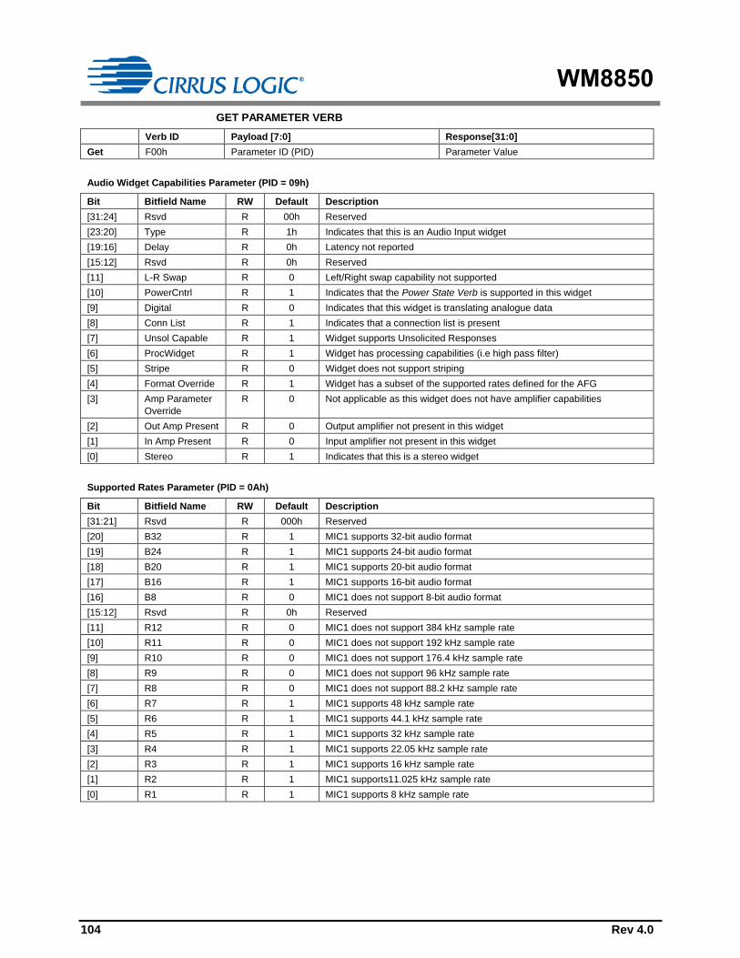
WM8850
104 Rev 4.0
GET PARAMETER VERB
Verb ID Payload [7:0] Response[31:0]
Get F00h Parameter ID (PID) Parameter Value
Audio Widget Capabilities Parameter (PID = 09h)
Bit Bitfield Name RW Default Description
[31:24] Rsvd R 00h Reserved
[23:20] Type R 1h Indicates that this is an Audio Input widget
[19:16] Delay R 0h Latency not reported
[15:12] Rsvd R 0h Reserved
[11] L-R Swap R 0 Left/Right swap capability not supported
[10] PowerCntrl R 1 Indicates that the Power State Verb is supported in this widget
[9] Digital R 0 Indicates that this widget is translating analogue data
[8] Conn List R 1 Indicates that a connection list is present
[7] Unsol Capable R 1 Widget supports Unsolicited Responses
[6] ProcWidget R 1 Widget has processing capabilities (i.e high pass filter)
[5] Stripe R 0 Widget does not support striping
[4] Format Override R 1 Widget has a subset of the supported rates defined for the AFG
[3] Amp Parameter
Override
R 0 Not applicable as this widget does not have amplifier capabilities
[2] Out Amp Present R 0 Output amplifier not present in this widget
[1] In Amp Present R 0 Input amplifier not present in this widget
[0] Stereo R 1 Indicates that this is a stereo widget
Supported Rates Parameter (PID = 0Ah)
Bit Bitfield Name RW Default Description
[31:21] Rsvd R 000h Reserved
[20] B32 R 1 MIC1 supports 32-bit audio format
[19] B24 R 1 MIC1 supports 24-bit audio format
[18] B20 R 1 MIC1 supports 20-bit audio format
[17] B16 R 1 MIC1 supports 16-bit audio format
[16] B8 R 0 MIC1 does not support 8-bit audio format
[15:12] Rsvd R 0h Reserved
[11] R12 R 0 MIC1 does not support 384 kHz sample rate
[10] R11 R 0 MIC1 does not support 192 kHz sample rate
[9] R10 R 0 MIC1 does not support 176.4 kHz sample rate
[8] R9 R 0 MIC1 does not support 96 kHz sample rate
[7] R8 R 0 MIC1 does not support 88.2 kHz sample rate
[6] R7 R 1 MIC1 supports 48 kHz sample rate
[5] R6 R 1 MIC1 supports 44.1 kHz sample rate
[4] R5 R 1 MIC1 supports 32 kHz sample rate
[3] R4 R 1 MIC1 supports 22.05 kHz sample rate
[2] R3 R 1 MIC1 supports 16 kHz sample rate
[1] R2 R 1 MIC1 supports11.025 kHz sample rate
[0] R1 R 1 MIC1 supports 8 kHz sample rate

WM8850
Rev 4.0 105
00h
01h
02h
03h
04h
05h
06h
07h
08h
09h
0Ah
0Bh
0Ch
0Dh
0Eh
0Fh
10h
11h
12h
13h
14h
15h
16h
17h
Supported Stream Formats Parameter (PID = 0Bh)
Bit Bitfield Name RW Default Description
[31:3] Rsvd R 00000000h Reserved
[2] AC3 R 0 MIC1 does not support Dolby AC3 formatted data
[1] Float32 R 1 MIC1 supports Float32 formatted data
[0] PCM R 1 MIC1 supports PCM formatted data
Connection List Length Parameter (PID = 0Eh)
Bit Bitfield Name RW Default Description
[31:8] Rsvd R 000000h Reserved
[7] Long Form R 0 Indicates that the connection list items are in short form
[6:0] Connection List
Length
R 01h Indicates that there is 1 NID entry in the connection list
Supported Power States Parameter (PID = 0Fh)
Bit Bitfield Name RW Default Description
[31:4] Rsvd R 0000000h Reserved
[3] D3Sup R 1 D3 power state supported
[2] D2Sup R 1 D2 power state supported
[1] D1sup R 1 D1 power state supported
[0] D0Sup R 1 D0 power state supported
Processing Capabilities Parameter (PID = 10h)
Bit Bitfield Name RW Default Description
[31:16] Rsvd R 0000h Reserved
[15:8] NumCoeff R 00h This widget does not support loadable coefficients
[7:1] Rsvd R 00h Reserved
[0] Benign R 0 The “Processing Benign State” is not supported
GET CONNECTION LIST ENTRY VERB
Verb ID Payload [7:0] Response[31:0]
Get F02h 00h Bits [31:0] in the table below
Bit Bitfield Name RW Default Description
[31:24] Conn List Entry 3 R 00h Unused connection list entry
[23:16] Conn List Entry 2 R 00h Unused connection list entry
[15:8] Conn List Entry 1 R 00h Unused connection list entry
[7:0] Conn List Entry 0 R 09h Indicates that the MIC1 Widget connects to the MIC1 Mux Widget (NID =
09h)
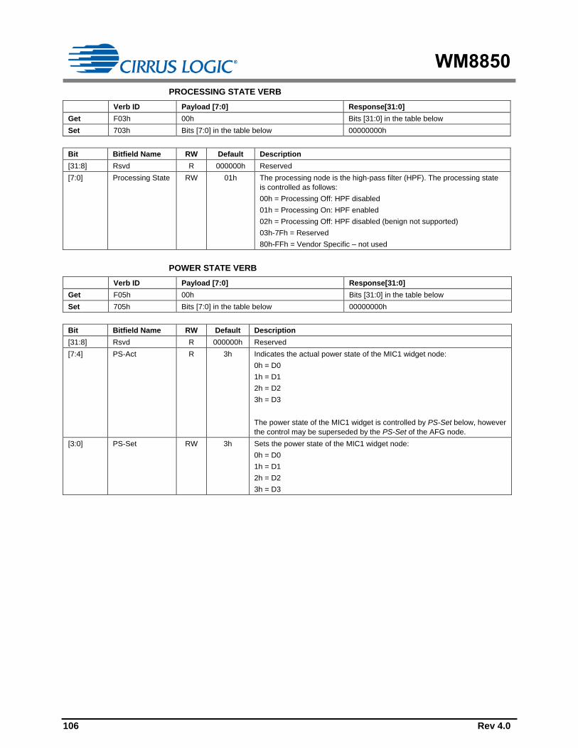
WM8850
106 Rev 4.0
PROCESSING STATE VERB
Verb ID Payload [7:0] Response[31:0]
Get F03h 00h Bits [31:0] in the table below
Set 703h Bits [7:0] in the table below 00000000h
Bit Bitfield Name RW Default Description
[31:8] Rsvd R 000000h Reserved
[7:0] Processing State RW 01h The processing node is the high-pass filter (HPF). The processing state
is controlled as follows:
00h = Processing Off: HPF disabled
01h = Processing On: HPF enabled
02h = Processing Off: HPF disabled (benign not supported)
03h-7Fh = Reserved
80h-FFh = Vendor Specific – not used
POWER STATE VERB
Verb ID Payload [7:0] Response[31:0]
Get F05h 00h Bits [31:0] in the table below
Set 705h Bits [7:0] in the table below 00000000h
Bit Bitfield Name RW Default Description
[31:8] Rsvd R 000000h Reserved
[7:4] PS-Act R 3h Indicates the actual power state of the MIC1 widget node:
0h = D0
1h = D1
2h = D2
3h = D3
The power state of the MIC1 widget is controlled by PS-Set below, however
the control may be superseded by the PS-Set of the AFG node.
[3:0] PS-Set RW 3h Sets the power state of the MIC1 widget node:
0h = D0
1h = D1
2h = D2
3h = D3
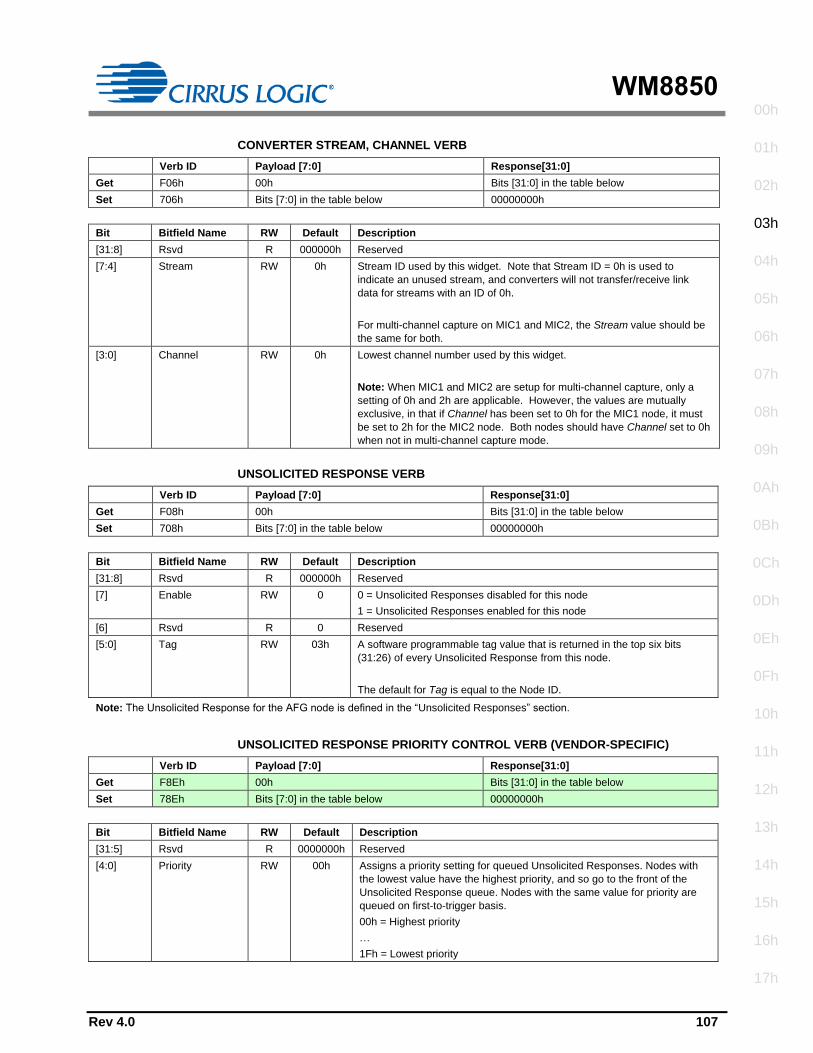
WM8850
Rev 4.0 107
00h
01h
02h
03h
04h
05h
06h
07h
08h
09h
0Ah
0Bh
0Ch
0Dh
0Eh
0Fh
10h
11h
12h
13h
14h
15h
16h
17h
CONVERTER STREAM, CHANNEL VERB
Verb ID Payload [7:0] Response[31:0]
Get F06h 00h Bits [31:0] in the table below
Set 706h Bits [7:0] in the table below 00000000h
Bit Bitfield Name RW Default Description
[31:8] Rsvd R 000000h Reserved
[7:4] Stream RW 0h Stream ID used by this widget. Note that Stream ID = 0h is used to
indicate an unused stream, and converters will not transfer/receive link
data for streams with an ID of 0h.
For multi-channel capture on MIC1 and MIC2, the Stream value should be
the same for both.
[3:0] Channel RW 0h Lowest channel number used by this widget.
Note: When MIC1 and MIC2 are setup for multi-channel capture, only a
setting of 0h and 2h are applicable. However, the values are mutually
exclusive, in that if Channel has been set to 0h for the MIC1 node, it must
be set to 2h for the MIC2 node. Both nodes should have Channel set to 0h
when not in multi-channel capture mode.
UNSOLICITED RESPONSE VERB
Verb ID Payload [7:0] Response[31:0]
Get F08h 00h Bits [31:0] in the table below
Set 708h Bits [7:0] in the table below 00000000h
Bit Bitfield Name RW Default Description
[31:8] Rsvd R 000000h Reserved
[7] Enable RW 0 0 = Unsolicited Responses disabled for this node
1 = Unsolicited Responses enabled for this node
[6] Rsvd R 0 Reserved
[5:0] Tag RW 03h A software programmable tag value that is returned in the top six bits
(31:26) of every Unsolicited Response from this node.
The default for Tag is equal to the Node ID.
Note: The Unsolicited Response for the AFG node is defined in the “Unsolicited Responses” section.
UNSOLICITED RESPONSE PRIORITY CONTROL VERB (VENDOR-SPECIFIC)
Verb ID Payload [7:0] Response[31:0]
Get F8Eh 00h Bits [31:0] in the table below
Set 78Eh Bits [7:0] in the table below 00000000h
Bit Bitfield Name RW Default Description
[31:5] Rsvd R 0000000h Reserved
[4:0] Priority RW 00h Assigns a priority setting for queued Unsolicited Responses. Nodes with
the lowest value have the highest priority, and so go to the front of the
Unsolicited Response queue. Nodes with the same value for priority are
queued on first-to-trigger basis.
00h = Highest priority
…
1Fh = Lowest priority
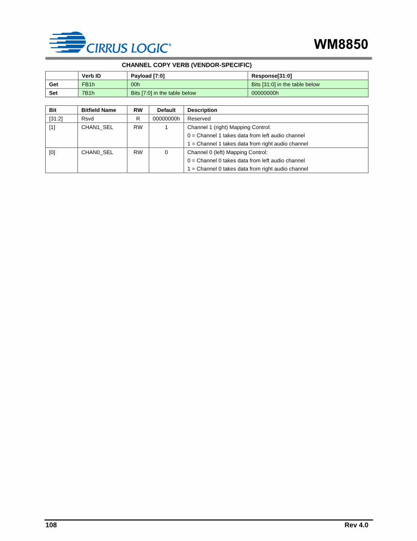
WM8850
108 Rev 4.0
CHANNEL COPY VERB (VENDOR-SPECIFIC)
Verb ID Payload [7:0] Response[31:0]
Get FB1h 00h Bits [31:0] in the table below
Set 7B1h Bits [7:0] in the table below 00000000h
Bit Bitfield Name RW Default Description
[31:2] Rsvd R 00000000h Reserved
[1] CHAN1_SEL RW 1 Channel 1 (right) Mapping Control:
0 = Channel 1 takes data from left audio channel
1 = Channel 1 takes data from right audio channel
[0] CHAN0_SEL RW 0 Channel 0 (left) Mapping Control:
0 = Channel 0 takes data from left audio channel
1 = Channel 0 takes data from right audio channel

WM8850
Rev 4.0 109
00h
01h
02h
03h
04h
05h
06h
07h
08h
09h
0Ah
0Bh
0Ch
0Dh
0Eh
0Fh
10h
11h
12h
13h
14h
15h
16h
17h
S/PDIF TX 1 AUDIO OUTPUT CONVERTER WIDGET (NID = 04H)
STREAM FORMAT VERB
Verb ID Payload [15:0] Response[31:0]
Get Ah 0000h Bits [31:0] in the table below
Set 2h Bits [15:0] in the table below 00000000h
Bit Bitfield Name RW Default Description
[31:16] Rsvd R 0000h Reserved
[15] Type RW 0 Used to set the format of the stream:
0 = PCM
1 = Non-PCM (i.e. AC3 or Software Formatted S/PDIF)
[14] Base RW 0 Used to set the base rate frequency:
0h = 48 kHz
1h = 44.1 kHz
[13:11] Mult RW 0h Used to set the base rate multiplication factor:
0h = x1 (48kHz, 44.1kHz or less)
1h = x2 (96kHz, 88.2kHz, 32kHz)
2h = Reserved
3h = x4 (192kHz, 176.4kHz)
4h-7h = Reserved
[10:8] Div RW 0h Used to set the base rate division factor:
0h = divide by 1 (48kHz, 44.1kHz)
1h =Reserved
2h = divide by 3 (32kHz)
3h-7h = Reserved
[7] Rsvd R 0 Reserved
[6:4] Bits RW 4h Bits per Sample:
0h = Reserved
1h = 16 bits
2h = 20 bits
3h = 24 bits
4h = 32 bits (Software Formatted or Float 32)
5h-7h = Reserved
[3:0] Chan RW 1h Number of Channels in each frame of the stream:
0h = 1 channel
1h = 2 channels
2h-Fh = reserved
Notes:
1. When the internal path (of ADC1 or MIC1 or MIC2) to S/PDIF TX 1 is active, Mult, Base & Div become read only and are
programmed by the WM8850 to match the sourced node settings.
2. When Software Formatted S/PDIF is selected, and the S/PDIF TX 1 is sourcing the HDA Link, the S/PDIF output is
driven low until stream ID is assigned.

WM8850
110 Rev 4.0
GET PARAMETER VERB
Verb ID Payload [7:0] Response[31:0]
Get F00h Parameter ID (PID) Parameter Value
Audio Widget Capabilities Parameter (PID = 09h)
Bit Bitfield Name RW Default Description
[31:24] Rsvd R 00h Reserved
[23:20] Type R 0h Indicates that this is an Audio Output Widget
[19:16] Delay R 0h Latency not reported
[15:12] Rsvd R 0h Reserved
[11] L-R Swap R 0 Left/Right swap capability not supported
[10] PowerCntrl R 0 Indicates that the Power State Verb is supported in this widget
[9] Digital R 1 Indicates that this widget is translating digital data
[8] Conn List R 0 Indicates that a connection list is not present
[7] Unsol Capable R 1 Widget supports Unsolicited Responses
[6] ProcWidget R 1 Widget has processing capabilities (i.e SRC2)
[5] Stripe R 0 Widget does not support striping
[4] Format Override R 1 Widget has a subset of the supported rates defined for the AFG
[3] Amp Parameter
Override
R 0 Not applicable as this widget does not have amplifier capabilities
[2] Out Amp Present R 0 Output amplifier not present in this widget
[1] In Amp Present R 0 Input amplifier not present in this widget
[0] Stereo R 1 Indicates that this is a stereo widget
Supported Rates Parameter (PID = 0Ah)
Bit Bitfield Name RW Default Description
[31:21] Rsvd R 000h Reserved
[20] B32 R 1 Float32 and Software Formatted S/PDIF is supported.
[19] B24 R 1 S/PDIF Tx 1 supports 24-bit audio format
[18] B20 R 1 S/PDIF Tx 1 supports 20-bit audio format
[17] B16 R 1 S/PDIF Tx 1 supports 16-bit audio format
[16] B8 R 0 S/PDIF Tx 1 does not support 8-bit audio format
[15:12] Rsvd R 0h Reserved
[11] R12 R 0 S/PDIF Tx 1 does not support 384 kHz sample rate
[10] R11 R 1 S/PDIF Tx 1 supports 192 kHz sample rate
[9] R10 R 1 S/PDIF Tx 1 supports 176.4 kHz sample rate
[8] R9 R 1 S/PDIF Tx 1 supports 96 kHz sample rate
[7] R8 R 1 S/PDIF Tx 1 supports 88.2 kHz sample rate
[6] R7 R 1 S/PDIF Tx 1 supports 48 kHz sample rate
[5] R6 R 1 S/PDIF Tx 1 supports 44.1 kHz sample rate
[4] R5 R 1 S/PDIF Tx 1 supports 32 kHz sample rate
[3] R4 R 0 S/PDIF Tx 1 does not support 22.05 kHz sample rate
[2] R3 R 0 S/PDIF Tx 1 does not support 16 kHz sample rate
[1] R2 R 0 S/PDIF Tx 1 does not support 11.025 kHz sample rate
[0] R1 R 0 S/PDIF Tx 1 does not support 8 kHz sample rate
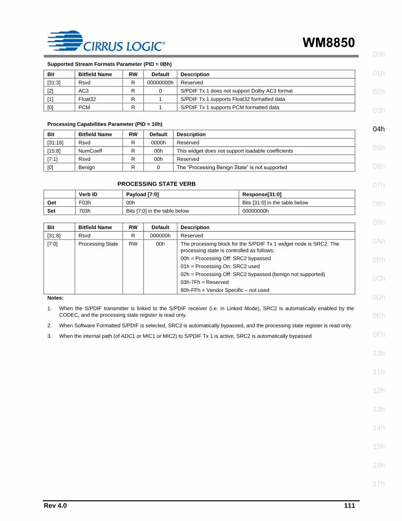
WM8850
Rev 4.0 111
00h
01h
02h
03h
04h
05h
06h
07h
08h
09h
0Ah
0Bh
0Ch
0Dh
0Eh
0Fh
10h
11h
12h
13h
14h
15h
16h
17h
Supported Stream Formats Parameter (PID = 0Bh)
Bit Bitfield Name RW Default Description
[31:3] Rsvd R 00000000h Reserved
[2] AC3 R 0 S/PDIF Tx 1 does not support Dolby AC3 format
[1] Float32 R 1 S/PDIF Tx 1 supports Float32 formatted data
[0] PCM R 1 S/PDIF Tx 1 supports PCM formatted data
Processing Capabilities Parameter (PID = 10h)
Bit Bitfield Name RW Default Description
[31:16] Rsvd R 0000h Reserved
[15:8] NumCoeff R 00h This widget does not support loadable coefficients
[7:1] Rsvd R 00h Reserved
[0] Benign R 0 The “Processing Benign State” is not supported
PROCESSING STATE VERB
Verb ID Payload [7:0] Response[31:0]
Get F03h 00h Bits [31:0] in the table below
Set 703h Bits [7:0] in the table below 00000000h
Bit Bitfield Name RW Default Description
[31:8] Rsvd R 000000h Reserved
[7:0] Processing State RW 00h The processing block for the S/PDIF Tx 1 widget node is SRC2. The
processing state is controlled as follows:
00h = Processing Off: SRC2 bypassed
01h = Processing On: SRC2 used
02h = Processing Off: SRC2 bypassed (benign not supported)
03h-7Fh = Reserved
80h-FFh = Vendor Specific – not used
Notes:
1. When the S/PDIF transmitter is linked to the S/PDIF receiver (i.e. in Linked Mode), SRC2 is automatically enabled by the
CODEC, and the processing state register is read only.
2. When Software Formatted S/PDIF is selected, SRC2 is automatically bypassed, and the processing state register is read only.
3. When the internal path (of ADC1 or MIC1 or MIC2) to S/PDIF Tx 1 is active, SRC2 is automatically bypassed
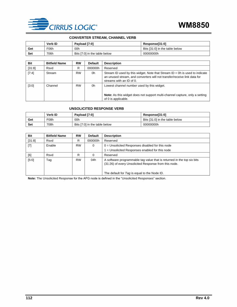
WM8850
112 Rev 4.0
CONVERTER STREAM, CHANNEL VERB
Verb ID Payload [7:0] Response[31:0]
Get F06h 00h Bits [31:0] in the table below
Set 706h Bits [7:0] in the table below 00000000h
Bit Bitfield Name RW Default Description
[31:8] Rsvd R 000000h Reserved
[7:4] Stream RW 0h Stream ID used by this widget. Note that Stream ID = 0h is used to indicate
an unused stream, and converters will not transfer/receive link data for
streams with an ID of 0.
[3:0] Channel RW 0h Lowest channel number used by this widget.
Note: As this widget does not support multi-channel capture, only a setting
of 0 is applicable.
UNSOLICITED RESPONSE VERB
Verb ID Payload [7:0] Response[31:0]
Get F08h 00h Bits [31:0] in the table below
Set 708h Bits [7:0] in the table below 00000000h
Bit Bitfield Name RW Default Description
[31:8] Rsvd R 000000h Reserved
[7] Enable RW 0 0 = Unsolicited Responses disabled for this node
1 = Unsolicited Responses enabled for this node
[6] Rsvd R 0 Reserved
[5:0] Tag RW 04h A software programmable tag value that is returned in the top six bits
(31:26) of every Unsolicited Response from this node.
The default for Tag is equal to the Node ID.
Note: The Unsolicited Response for the AFG node is defined in the “Unsolicited Responses” section.

WM8850
Rev 4.0 113
00h
01h
02h
03h
04h
05h
06h
07h
08h
09h
0Ah
0Bh
0Ch
0Dh
0Eh
0Fh
10h
11h
12h
13h
14h
15h
16h
17h
S/PDIF CONVERTER CONTROL VERB
Verb ID Payload [7:0] Response[31:0]
Get F0Dh 0000h Bits [31:0] in the table below
Set1 70Dh Bits [7:0] in the table below 00000000h
Set2 70Eh Bits [15:8] in the table below 00000000h
Bit Bitfield Name RW Default Description
[31:15] Rsvd R 00000h Reserved
[14:8] CC RW 00h Category Code. Channel Status bits [14:8] – see IEC 60958-3 for details.
[7] L RW 0 Generation Level, Channel Status bit [15] - see IEC 60958-3 for details.
[6] PRO RW 0 Professional, Channel Status bit[0]:
0 = Consumer Channel Status (40-bits)
1 = Professional Channel Status (192-bits )
[5] /AUDIO RW 0 Non-Audio, Channel Status bit[1]:
0 = PCM formatted data
1 = non-PCM formatted data
[4] COPY RW 0 Copyright, Channel Status bit[2]:
0 = indicates copyright asserted (i.e. S/PDIF Channel Status bit[2] set to
1)
1 = indicates no copyright asserted (i.e. S/PDIF Channel Status bit[2] set
to 0)
Note: The HDA specifiction, and the IEC 60958-3 specification are the
inverse of each other. To comply with both, the WM8850 inverts the
written value.
[3] PRE RW 0 Pre-emphasis, Channel Status bit[3]:
0 = no pre-emphasis
1 = 50/15 us pre-emphasis
[2] VCFG RW 0 Validity Configuration Control - determines what happens to the audio
data, should an invalid sample occur (invalid samples occur when SRC2
is in use but not locked, EF_STREAM_ERR is asserted, or the stream ID
is 0).
0 = pass data as received by the S/PDIF Tx 1.
1 = overwrite invalid data with all zeros (for the invalid sub frame only).
[1] V RW 0 Validity:
0 = Indicates valid data
1 = Indicates invalid data
If V=1, the transmitted validity flag is set to 1.
If V=0, the transmitted validity flag is set to 1 if there is an invalid sample
being transmitted. Invalid samples may occur when SRC2 is in use but
not locked, EF_STREAM_ERR is asserted, or the stream ID is 0.
[0] DigEn RW 0 Digital Enable:
0 = S/PDIF audio path disabled
1 = S/PDIF audio path enabled
Note: When Software Formatted S/PDIF is selected, verb settings for channel status and validity are not used
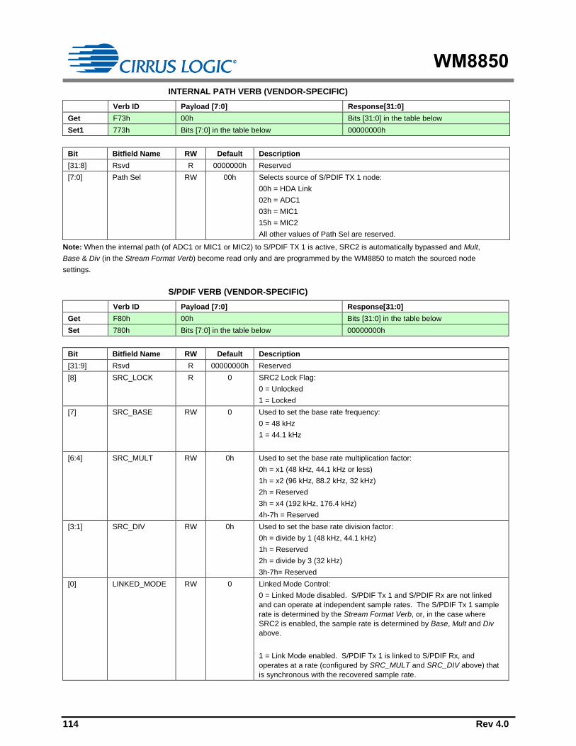
WM8850
114 Rev 4.0
INTERNAL PATH VERB (VENDOR-SPECIFIC)
Verb ID Payload [7:0] Response[31:0]
Get F73h 00h Bits [31:0] in the table below
Set1 773h Bits [7:0] in the table below 00000000h
Bit Bitfield Name RW Default Description
[31:8] Rsvd R 0000000h Reserved
[7:0] Path Sel RW 00h Selects source of S/PDIF TX 1 node:
00h = HDA Link
02h = ADC1
03h = MIC1
15h = MIC2
All other values of Path Sel are reserved.
Note: When the internal path (of ADC1 or MIC1 or MIC2) to S/PDIF TX 1 is active, SRC2 is automatically bypassed and Mult,
Base & Div (in the Stream Format Verb) become read only and are programmed by the WM8850 to match the sourced node
settings.
S/PDIF VERB (VENDOR-SPECIFIC)
Verb ID Payload [7:0] Response[31:0]
Get F80h 00h Bits [31:0] in the table below
Set 780h Bits [7:0] in the table below 00000000h
Bit Bitfield Name RW Default Description
[31:9] Rsvd R 00000000h Reserved
[8] SRC_LOCK R 0 SRC2 Lock Flag:
0 = Unlocked
1 = Locked
[7] SRC_BASE RW 0 Used to set the base rate frequency:
0 = 48 kHz
1 = 44.1 kHz
[6:4] SRC_MULT RW 0h Used to set the base rate multiplication factor:
0h = x1 (48 kHz, 44.1 kHz or less)
1h = x2 (96 kHz, 88.2 kHz, 32 kHz)
2h = Reserved
3h = x4 (192 kHz, 176.4 kHz)
4h-7h = Reserved
[3:1] SRC_DIV RW 0h Used to set the base rate division factor:
0h = divide by 1 (48 kHz, 44.1 kHz)
1h = Reserved
2h = divide by 3 (32 kHz)
3h-7h= Reserved
[0] LINKED_MODE RW 0 Linked Mode Control:
0 = Linked Mode disabled. S/PDIF Tx 1 and S/PDIF Rx are not linked
and can operate at independent sample rates. The S/PDIF Tx 1 sample
rate is determined by the Stream Format Verb, or, in the case where
SRC2 is enabled, the sample rate is determined by Base, Mult and Div
above.
1 = Link Mode enabled. S/PDIF Tx 1 is linked to S/PDIF Rx, and
operates at a rate (configured by SRC_MULT and SRC_DIV above) that
is synchronous with the recovered sample rate.

WM8850
Rev 4.0 115
00h
01h
02h
03h
04h
05h
06h
07h
08h
09h
0Ah
0Bh
0Ch
0Dh
0Eh
0Fh
10h
11h
12h
13h
14h
15h
16h
17h
TX CHANNEL STATUS CONTROL VERB (VENDOR-SPECIFIC)
Verb ID Payload [7:0] Response[31:0]
Get F81h 00h Bits [31:0] in the table below
Set1 781h Bits [7:0] in the table below 00000000h
Set2 782h Bits [15:8] in the table below 00000000h
Set3 783h Bits [23:16] in the table below 00000000h
Set4 784h Bits [31:24] in the table below 00000000h
The bits in the table below are defined in the IEC-60958-3 Specification:
Bit Bitfield Name RW Default Description
[31:28] Channel Status
[39:36]
RW 0h Original Sampling Frequency
[27:25] Channel Status
[35:33]
RW 5h Sample Word Length
[24] Channel Status
[32]
RW 1 Max Word Length
[23:22] Channel Status
[31:30]
RW 0h Channel Status [31:30]
[21:20] Channel Status
[29:28]
RW 0h Clock Accuracy
[19:16] Channel Status
[27:24]
RW 1h Sampling Frequency
[15:12] Channel Status
B [23:20]
RW 0h Channel Number for Sub-Frame B
[11:8] Channel Status
[23:20]
RW 0h Channel Number for Sub-Frame A
[7:4] Channel Status
[19:16]
RW 0h Source Number
[3:2] Channel Status
[7:6]
RW 0h Channel Status Mode
[1:0] Channel Status
[5:4]
RW 0h Additional De-emphasis Information
Notes:
1. When Software Formatted S/PDIF is selected, verb settings for channel status and validity are not used.
2. The Channel Number for Sub-frame B is uniquely configurable – all other Channel status bits have the same value as
Sub-frame A.
CHANNEL STATUS DATA PACKING CONFIGURATION VERB (VENDOR-SPECIFIC)
Verb ID Payload [7:0] Response[31:0]
Get F85h 00h Bits [31:0] in the table below
Set 785h Bits [7:0] in the table below 00000000h
Bit Bitfield Name RW Default Description
[31:1] Rsvd R 0000000h Reserved
[0] CSD_MODE RW 1 S/PDIF Transmitter Channel Status Data Packing Mode:
0 = Manual mode: sample rate and data width channel status data
packed from data sourced from the Tx Channel Status Control Verb
1 = Automatic mode: sample rate and data width channel status data
packed from data sourced from the Stream Verb, S/PDIF Verb or S/PDIF
Rx Rate Detector (depending on routing through device)

WM8850
116 Rev 4.0
UNSOLICITED RESPONSE PRIORITY CONTROL VERB (VENDOR-SPECIFIC)
Verb ID Payload [7:0] Response[31:0]
Get F8Eh 00h Bits [31:0] in the table below
Set 78Eh Bits [7:0] in the table below 00000000h
Bit Bitfield Name RW Default Description
[31:5] Rsvd R 0000000h Reserved
[4:0] Priority RW 00h Assigns a priority setting for queued Unsolicited Responses. Nodes with
the lowest value have the highest priority, and so go to the front of the
Unsolicited Response queue. Nodes with the same value for priority are
queued on first-to-trigger basis.
00h = Highest priority
…
1Fh = Lowest priority
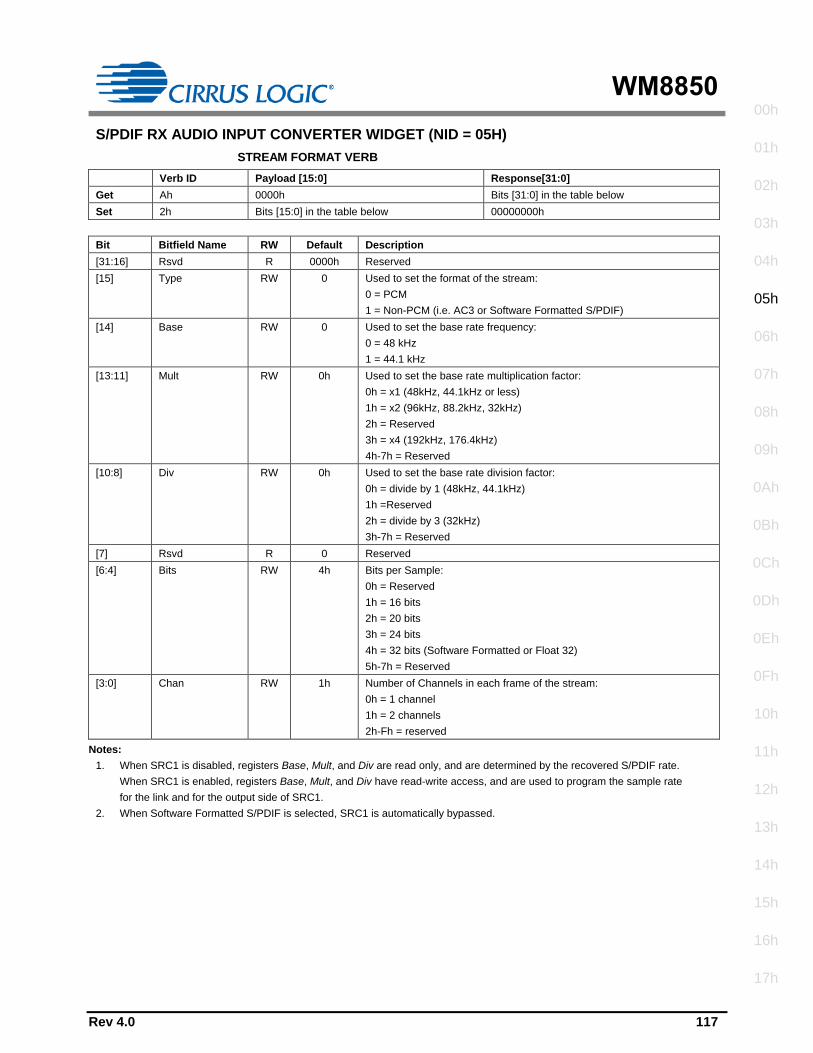
WM8850
Rev 4.0 117
00h
01h
02h
03h
04h
05h
06h
07h
08h
09h
0Ah
0Bh
0Ch
0Dh
0Eh
0Fh
10h
11h
12h
13h
14h
15h
16h
17h
S/PDIF RX AUDIO INPUT CONVERTER WIDGET (NID = 05H)
STREAM FORMAT VERB
Verb ID Payload [15:0] Response[31:0]
Get Ah 0000h Bits [31:0] in the table below
Set 2h Bits [15:0] in the table below 00000000h
Bit Bitfield Name RW Default Description
[31:16] Rsvd R 0000h Reserved
[15] Type RW 0 Used to set the format of the stream:
0 = PCM
1 = Non-PCM (i.e. AC3 or Software Formatted S/PDIF)
[14] Base RW 0 Used to set the base rate frequency:
0 = 48 kHz
1 = 44.1 kHz
[13:11] Mult RW 0h Used to set the base rate multiplication factor:
0h = x1 (48kHz, 44.1kHz or less)
1h = x2 (96kHz, 88.2kHz, 32kHz)
2h = Reserved
3h = x4 (192kHz, 176.4kHz)
4h-7h = Reserved
[10:8] Div RW 0h Used to set the base rate division factor:
0h = divide by 1 (48kHz, 44.1kHz)
1h =Reserved
2h = divide by 3 (32kHz)
3h-7h = Reserved
[7] Rsvd R 0 Reserved
[6:4] Bits RW 4h Bits per Sample:
0h = Reserved
1h = 16 bits
2h = 20 bits
3h = 24 bits
4h = 32 bits (Software Formatted or Float 32)
5h-7h = Reserved
[3:0] Chan RW 1h Number of Channels in each frame of the stream:
0h = 1 channel
1h = 2 channels
2h-Fh = reserved
Notes:
1. When SRC1 is disabled, registers Base, Mult, and Div are read only, and are determined by the recovered S/PDIF rate.
When SRC1 is enabled, registers Base, Mult, and Div have read-write access, and are used to program the sample rate
for the link and for the output side of SRC1.
2. When Software Formatted S/PDIF is selected, SRC1 is automatically bypassed.
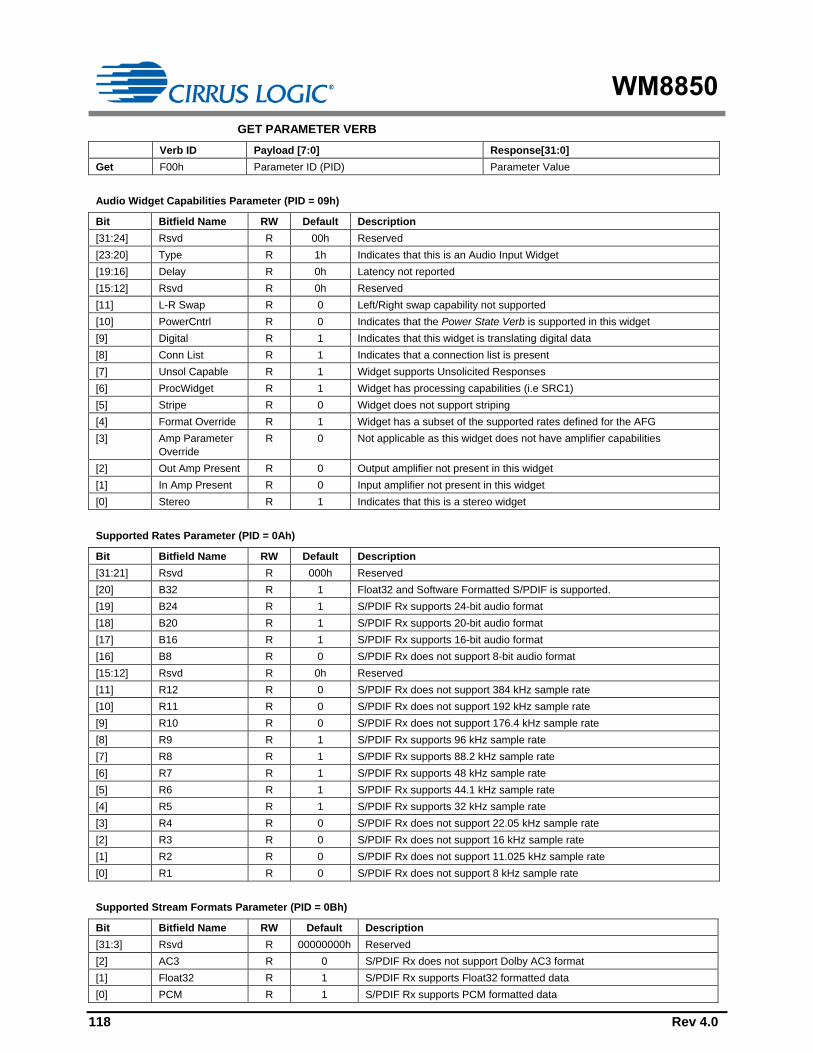
WM8850
118 Rev 4.0
GET PARAMETER VERB
Verb ID Payload [7:0] Response[31:0]
Get F00h Parameter ID (PID) Parameter Value
Audio Widget Capabilities Parameter (PID = 09h)
Bit Bitfield Name RW Default Description
[31:24] Rsvd R 00h Reserved
[23:20] Type R 1h Indicates that this is an Audio Input Widget
[19:16] Delay R 0h Latency not reported
[15:12] Rsvd R 0h Reserved
[11] L-R Swap R 0 Left/Right swap capability not supported
[10] PowerCntrl R 0 Indicates that the Power State Verb is supported in this widget
[9] Digital R 1 Indicates that this widget is translating digital data
[8] Conn List R 1 Indicates that a connection list is present
[7] Unsol Capable R 1 Widget supports Unsolicited Responses
[6] ProcWidget R 1 Widget has processing capabilities (i.e SRC1)
[5] Stripe R 0 Widget does not support striping
[4] Format Override R 1 Widget has a subset of the supported rates defined for the AFG
[3] Amp Parameter
Override
R 0 Not applicable as this widget does not have amplifier capabilities
[2] Out Amp Present R 0 Output amplifier not present in this widget
[1] In Amp Present R 0 Input amplifier not present in this widget
[0] Stereo R 1 Indicates that this is a stereo widget
Supported Rates Parameter (PID = 0Ah)
Bit Bitfield Name RW Default Description
[31:21] Rsvd R 000h Reserved
[20] B32 R 1 Float32 and Software Formatted S/PDIF is supported.
[19] B24 R 1 S/PDIF Rx supports 24-bit audio format
[18] B20 R 1 S/PDIF Rx supports 20-bit audio format
[17] B16 R 1 S/PDIF Rx supports 16-bit audio format
[16] B8 R 0 S/PDIF Rx does not support 8-bit audio format
[15:12] Rsvd R 0h Reserved
[11] R12 R 0 S/PDIF Rx does not support 384 kHz sample rate
[10] R11 R 0 S/PDIF Rx does not support 192 kHz sample rate
[9] R10 R 0 S/PDIF Rx does not support 176.4 kHz sample rate
[8] R9 R 1 S/PDIF Rx supports 96 kHz sample rate
[7] R8 R 1 S/PDIF Rx supports 88.2 kHz sample rate
[6] R7 R 1 S/PDIF Rx supports 48 kHz sample rate
[5] R6 R 1 S/PDIF Rx supports 44.1 kHz sample rate
[4] R5 R 1 S/PDIF Rx supports 32 kHz sample rate
[3] R4 R 0 S/PDIF Rx does not support 22.05 kHz sample rate
[2] R3 R 0 S/PDIF Rx does not support 16 kHz sample rate
[1] R2 R 0 S/PDIF Rx does not support 11.025 kHz sample rate
[0] R1 R 0 S/PDIF Rx does not support 8 kHz sample rate
Supported Stream Formats Parameter (PID = 0Bh)
Bit Bitfield Name RW Default Description
[31:3] Rsvd R 00000000h Reserved
[2] AC3 R 0 S/PDIF Rx does not support Dolby AC3 format
[1] Float32 R 1 S/PDIF Rx supports Float32 formatted data
[0] PCM R 1 S/PDIF Rx supports PCM formatted data

WM8850
Rev 4.0 119
00h
01h
02h
03h
04h
05h
06h
07h
08h
09h
0Ah
0Bh
0Ch
0Dh
0Eh
0Fh
10h
11h
12h
13h
14h
15h
16h
17h
Connection List Length Parameter (PID = 0Eh)
Bit Bitfield Name RW Default Description
[31:8] Rsvd R 000000h Reserved
[7] Long Form R 0 Indicates that the connection list items are in short form
[6:0] Connection List
Length
R 01h Indicates that there is 1 NID entry in the connection list
Processing Capabilities Parameter (PID = 10h)
Bit Bitfield Name RW Default Description
[31:16] Rsvd R 0000h Reserved
[15:8] NumCoeff R 00h This widget does not support loadable coefficients
[7:1] Rsvd R 00h Reserved
[0] Benign R 0 The “Processing Benign State” is not supported
GET CONNECTION LIST ENTRY VERB
Verb ID Payload [7:0] Response[31:0]
Get F02h 00h Bits [31:0] in the table below
Bit Bitfield Name RW Default Description
[31:24] Conn List Entry 3 R 00h Unused connection list entry
[23:16] Conn List Entry 2 R 00h Unused connection list entry
[15:8] Conn List Entry 1 R 00h Unused connection list entry
[7:0] Conn List Entry 0 R 10h Indicates that the S/PDIF Rx Input Widget node connects to the
SPDIF_IN Pin Widget (NID = 10h)
PROCESSING STATE VERB
Verb ID Payload [7:0] Response[31:0]
Get F03h 00h Bits [31:0] in the table below
Set 703h Bits [7:0] in the table below 00000000h
Bit Bitfield Name RW Default Description
[31:8] Rsvd R 000000h Reserved
[7:0] Processing State RW 00h The processing block for the S/PDIF Rx widget node is SRC1. The
processing state is controlled as follows:
00h = Processing Off: SRC1 bypassed
01h = Processing On: SRC1 used
02h = Processing Off: SRC1 bypassed (benign not supported)
03h-7Fh = Reserved
80h-FFh = Vendor Specific – not used
Note:
The Processing State Verb should be set to 00h (SRC1 bypassed) when Software Formatted S/PDIF is selected or when any
S/PDIF Rx to DAC internal path is enabled. This is not done automatically.

WM8850
120 Rev 4.0
CONVERTER STREAM, CHANNEL VERB
Verb ID Payload [7:0] Response[31:0]
Get F06h 00h Bits [31:0] in the table below
Set 706h Bits [7:0] in the table below 00000000h
Bit Bitfield Name RW Default Description
[31:8] Rsvd R 000000h Reserved
[7:4] Stream RW 0h Stream ID used by this widget. Note that Stream ID = 0 is used to indicate
an unused stream, and converters will not transfer/receive link data for
streams with an ID of 0.
[3:0] Channel RW 0h Lowest channel number used by this widget.
Note: As this widget does not support multi-channel capture, only a setting
of 0 is applicable.
UNSOLICITED RESPONSE VERB
Verb ID Payload [7:0] Response[31:0]
Get F08h 00h Bits [31:0] in the table below
Set 708h Bits [7:0] in the table below 00000000h
Bit Bitfield Name RW Default Description
[31:8] Rsvd R 000000h Reserved
[7] Enable RW 0 0 = Unsolicited Responses disabled for this node
1 = Unsolicited Responses enabled for this node
[6] Rsvd R 0 Reserved
[5:0] Tag RW 05h A software programmable tag value that is returned in the top six bits
(31:26) of every Unsolicited Response from this node.
The default for Tag is equal to the Node ID.
Note: The Unsolicited Response for the AFG node is defined in the “Unsolicited Responses” section.
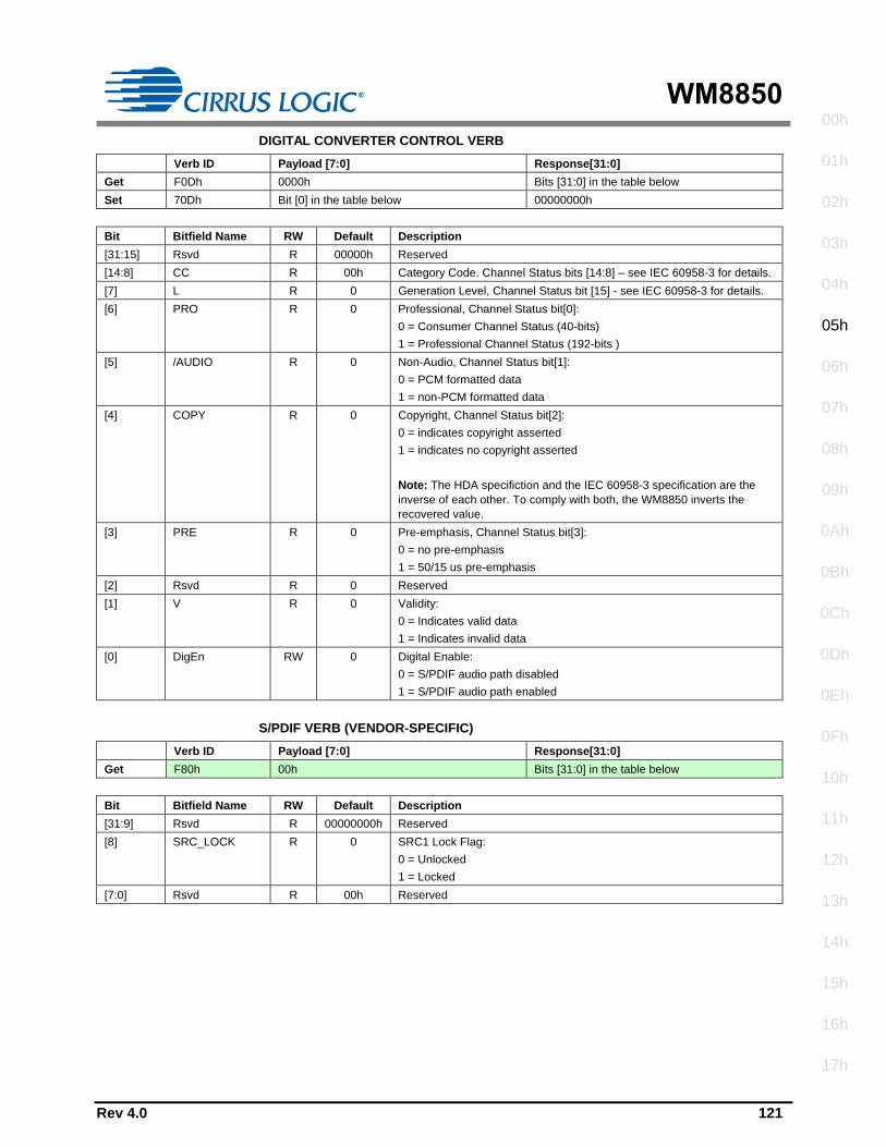
WM8850
Rev 4.0 121
00h
01h
02h
03h
04h
05h
06h
07h
08h
09h
0Ah
0Bh
0Ch
0Dh
0Eh
0Fh
10h
11h
12h
13h
14h
15h
16h
17h
DIGITAL CONVERTER CONTROL VERB
Verb ID Payload [7:0] Response[31:0]
Get F0Dh 0000h Bits [31:0] in the table below
Set 70Dh Bit [0] in the table below 00000000h
Bit Bitfield Name RW Default Description
[31:15] Rsvd R 00000h Reserved
[14:8] CC R 00h Category Code. Channel Status bits [14:8] – see IEC 60958-3 for details.
[7] L R 0 Generation Level, Channel Status bit [15] - see IEC 60958-3 for details.
[6] PRO R 0 Professional, Channel Status bit[0]:
0 = Consumer Channel Status (40-bits)
1 = Professional Channel Status (192-bits )
[5] /AUDIO R 0 Non-Audio, Channel Status bit[1]:
0 = PCM formatted data
1 = non-PCM formatted data
[4] COPY R 0 Copyright, Channel Status bit[2]:
0 = indicates copyright asserted
1 = indicates no copyright asserted
Note: The HDA specifiction and the IEC 60958-3 specification are the
inverse of each other. To comply with both, the WM8850 inverts the
recovered value.
[3] PRE R 0 Pre-emphasis, Channel Status bit[3]:
0 = no pre-emphasis
1 = 50/15 us pre-emphasis
[2] Rsvd R 0 Reserved
[1] V R 0 Validity:
0 = Indicates valid data
1 = Indicates invalid data
[0] DigEn RW 0 Digital Enable:
0 = S/PDIF audio path disabled
1 = S/PDIF audio path enabled
S/PDIF VERB (VENDOR-SPECIFIC)
Verb ID Payload [7:0] Response[31:0]
Get F80h 00h Bits [31:0] in the table below
Bit Bitfield Name RW Default Description
[31:9] Rsvd R 00000000h Reserved
[8] SRC_LOCK R 0 SRC1 Lock Flag:
0 = Unlocked
1 = Locked
[7:0] Rsvd R 00h Reserved

WM8850
122 Rev 4.0
UNSOLICITED RESPONSE PRIORITY CONTROL VERB (VENDOR-SPECIFIC)
Verb ID Payload [7:0] Response[31:0]
Get F8Eh 00h Bits [31:0] in the table below
Set 78Eh Bits [7:0] in the table below 00000000h
Bit Bitfield Name RW Default Description
[31:5] Rsvd R 0000000h Reserved
[4:0] Priority RW 00h Assigns a priority setting for queued Unsolicited Responses. Nodes with
the lowest value have the highest priority, and so go to the front of the
Unsolicited Response queue. Nodes with the same value for priority are
queued on first-to-trigger basis.
00h = Highest priority
…
1Fh = Lowest priority
GET CHANNEL STATUS VERB (VENDOR-SPECIFIC)
Verb ID Payload [7:0] Response[31:0]
Get F91h 00h Bits [31:0] in the table below
Get F91h 01h Bits [39:32] in the table below
The bits in the table below are defined in the IEC-60958-3 Specification:
Bit Bitfield Name RW Default Description
[39:36] Original
Sampling
Frequency
R N/A Original Sampling Frequency
[35:33] Sample Word
Length
R N/A Sample Word Length
[32] Max Word
Length
R N/A Max Word Length
[31:28] Clock Accuracy R N/A Clock Accuracy
[27:24] Sampling
Frequency
R N/A Sampling Frequency
[23:20] Channel Number R N/A Channel Number
[19:16] Source Number R N/A Source Number
[15:8] Category Code R N/A Category Code
[7:6] Channel Status
Mode
R N/A Channel Status Mode
[5:4] Additional De-
emphasis
Information
R N/A Additional De-emphasis Information
[3] PRE R N/A Pre-emphasis
[2] /COPY R N/A Copyright
[1] /AUDIO R N/A Non Audio
[0] PRO R N/A Professional/Consumer
GET NON-AUDIO FLAG VERB (VENDOR-SPECIFIC)
Verb ID Payload [7:0] Response[31:0]
Get F92h 00h Bits [31:0] in the table below
Bit Bitfield Name RW Default Description
[31:1] Rsvd R 00000000h Reserved
[0] Non Audio Flag R 0 Indicates the presence of the non-audio flag:
0 = non-audio flag not asserted
1 = non-audio flag asserted
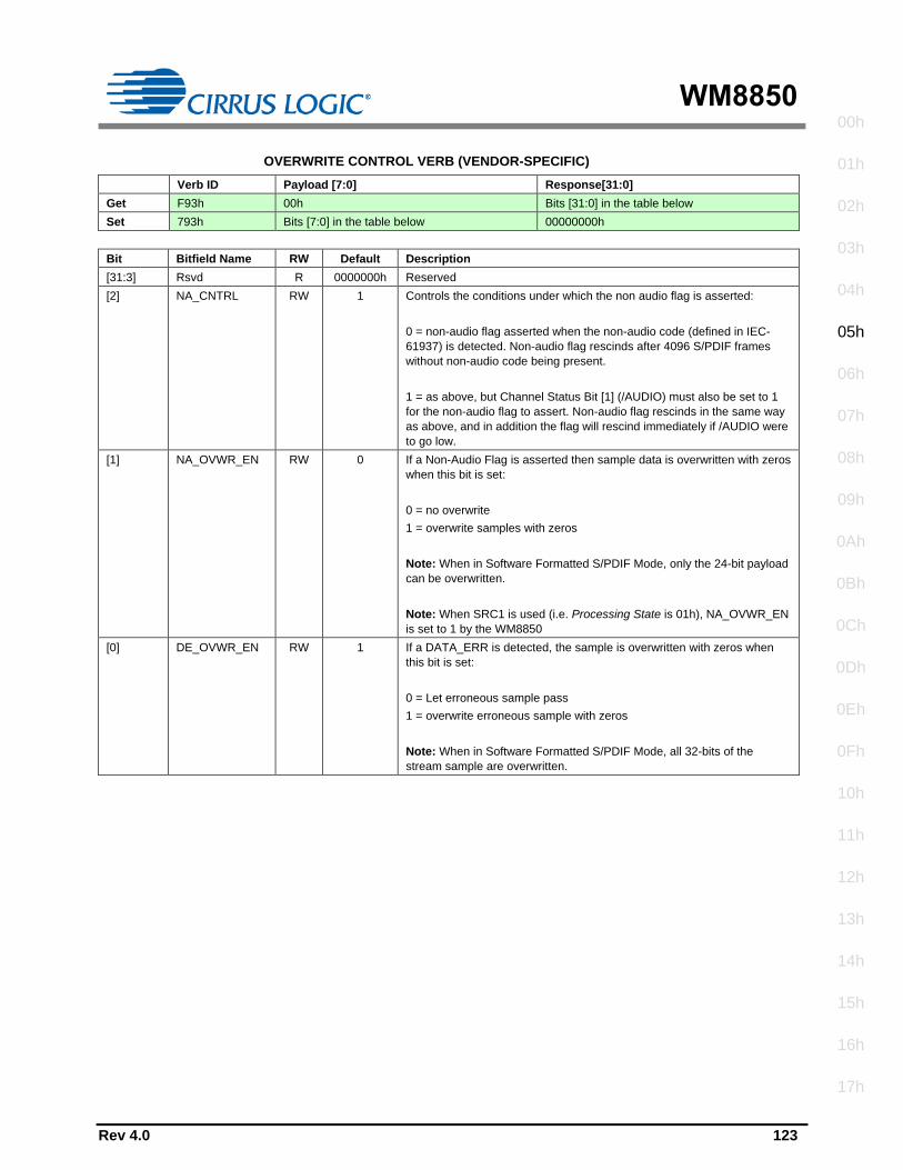
WM8850
Rev 4.0 123
00h
01h
02h
03h
04h
05h
06h
07h
08h
09h
0Ah
0Bh
0Ch
0Dh
0Eh
0Fh
10h
11h
12h
13h
14h
15h
16h
17h
OVERWRITE CONTROL VERB (VENDOR-SPECIFIC)
Verb ID Payload [7:0] Response[31:0]
Get F93h 00h Bits [31:0] in the table below
Set 793h Bits [7:0] in the table below 00000000h
Bit Bitfield Name RW Default Description
[31:3] Rsvd R 0000000h Reserved
[2] NA_CNTRL RW 1 Controls the conditions under which the non audio flag is asserted:
0 = non-audio flag asserted when the non-audio code (defined in IEC-
61937) is detected. Non-audio flag rescinds after 4096 S/PDIF frames
without non-audio code being present.
1 = as above, but Channel Status Bit [1] (/AUDIO) must also be set to 1
for the non-audio flag to assert. Non-audio flag rescinds in the same way
as above, and in addition the flag will rescind immediately if /AUDIO were
to go low.
[1] NA_OVWR_EN RW 0 If a Non-Audio Flag is asserted then sample data is overwritten with zeros
when this bit is set:
0 = no overwrite
1 = overwrite samples with zeros
Note: When in Software Formatted S/PDIF Mode, only the 24-bit payload
can be overwritten.
Note: When SRC1 is used (i.e. Processing State is 01h), NA_OVWR_EN
is set to 1 by the WM8850
[0] DE_OVWR_EN RW 1 If a DATA_ERR is detected, the sample is overwritten with zeros when
this bit is set:
0 = Let erroneous sample pass
1 = overwrite erroneous sample with zeros
Note: When in Software Formatted S/PDIF Mode, all 32-bits of the
stream sample are overwritten.

WM8850
124 Rev 4.0

WM8850
Rev 4.0 125
00h
01h
02h
03h
04h
05h
06h
07h
08h
09h
0Ah
0Bh
0Ch
0Dh
0Eh
0Fh
10h
11h
12h
13h
14h
15h
16h
17h
DAC1 AUDIO OUTPUT CONVERTER WIDGET (NID = 06H)
STREAM FORMAT VERB
Verb ID Payload [15:0] Response[31:0]
Get Ah 0000h Bits [31:0] in the table below
Set 2h Bits [15:0] in the table below 00000000h
Bit Bitfield Name RW Default Description
[31:16] Rsvd R 0000h Reserved
[15] Type R 0h Indicates the widget supports only PCM streams
[14] Base RW 0 Used to set the base rate frequency:
0 = 48 kHz
1 = 44.1 kHz
[13:11] Mult RW 0h Used to set the base rate multiplication factor:
0h = x1 (48kHz, 44.1kHz or less)
1h = x2 (96kHz, 88.2kHz, 32kHz)
2h = Reserved
3h = x4 (192kHz, 176.4kHz)
4h-7h = Reserved
[10:8] Div RW 0h Used to set the base rate division factor:
0h = divide by 1 (48kHz, 44.1kHz)
1h = divide by 2 (24kHz, 22.05kHz)
2h = divide by 3 (16kHz, 32kHz)
3h = divide by 4 (11.025kHz)
4h = Reserved
5h = divide by 6 (8kHz)
6h = Reserved
7h = Reserved
[7] Rsvd R 0 Reserved
[6:4] Bits RW 3h Bits per Sample:
0h = Reserved
1h = 16 bits
2h = 20 bits
3h = 24 bits
4h = 32 bits (Float 32)
5h-7h = Reserved
[3:0] Chan RW 1h Number of Channels in each frame of the stream:
0h = 1 channel
1h = 2 channels
2h = 3 channels
3h = 4 channels
4h = 5 channels
5h = 6 channels
6h-Fh = reserved
Note: When the internal path between the S/PDIF Rx node to the DAC1, DAC2 and DAC3 nodes is active, Mult, Base & Div
become read only and are programmed by the SPDIF_IN node to match the incoming sample rate.
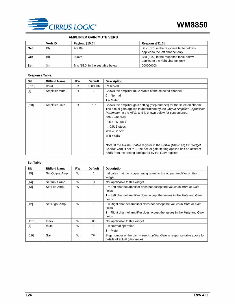
WM8850
126 Rev 4.0
AMPLIFIER GAIN/MUTE VERB
Verb ID Payload [15:0] Response[31:0]
Get Bh A000h Bits [31:0] in the response table below –
applies to the left channel only
Get Bh 8000h Bits [31:0] in the response table below –
applies to the right channel only
Set 3h Bits [15:0] in the set table below 00000000h
Response Table:
Bit Bitfield Name RW Default Description
[31:8] Rsvd R 000000h Reserved
[7] Amplifier Mute R 1 Shows the amplifier mute status of the selected channel:
0 = Normal
1 = Muted
[6:0] Amplifier Gain R 7Fh Shows the amplifier gain setting (step number) for the selected channel.
The actual gain applied is determined by the Output Amplifier Capabilities
Parameter in the AFG, and is shown below for convenience:
00h = −63.5dB
01h = −63.0dB
… 0.5dB steps
7Eh = −0.5dB
7Fh = 0dB
Note: If the H-Phn Enable register in the Port-A (NID=11h) Pin Widget
Control Verb is set to 1, the actual gain setting applied has an offset of
−8dB from the setting configured by the Gain register.
Set Table:
Bit Bitfield Name RW Default Description
[15] Set Output Amp W 1 Indicates that the programming refers to the output amplifier on this
widget
[14] Set Input Amp W 0 Not applicable to this widget
[13] Set Left Amp W 1 0 = Left channel amplifier does not accept the values in Mute or Gain
fields
1 = Left channel amplifier does accept the values in the Mute and Gain
fields
[12] Set Right Amp W 1 0 = Right channel amplifier does not accept the values in Mute or Gain
fields
1 = Right channel amplifier does accept the values in the Mute and Gain
fields
[11:8] Index W 0h Not applicable to this widget
[7] Mute W 1 0 = Normal operation
1 = Mute
[6:0] Gain W 7Fh Step number of the gain – see Amplifier Gain in response table above for
details of actual gain values

WM8850
Rev 4.0 127
00h
01h
02h
03h
04h
05h
06h
07h
08h
09h
0Ah
0Bh
0Ch
0Dh
0Eh
0Fh
10h
11h
12h
13h
14h
15h
16h
17h
GET PARAMETER VERB
Verb ID Payload [7:0] Response[31:0]
Get F00h Parameter ID (PID) Parameter Value
Audio Widget Capabilities Parameter (PID = 09h)
Bit Bitfield Name RW Default Description
[31:24] Rsvd R 00h Reserved
[23:20] Type R 0h Indicates that this is an Audio Output Widget
[19:16] Delay R 0h Latency not reported
[15:12] Rsvd R 0h Reserved
[11] L-R Swap R 0 Left/Right swap capability not supported
[10] PowerCntrl R 1 Indicates that the Power State Verb is supported in this widget
[9] Digital R 0 Indicates that this widget is translating analogue data
[8] Conn List R 0 Indicates that a connection list is not present
[7] Unsol Capable R 1 Widget supports Unsolicited Responses
[6] ProcWidget R 0 Widget does not have processing capabilities
[5] Stripe R 0 Widget does not support striping
[4] Format Override R 1 Widget has a subset of the supported rates defined for the AFG
[3] Amp Parameter
Override
R 0 The AFG amplifier parameters are used for this widget
[2] Out Amp Present R 1 Output amplifier is present in this widget
[1] In Amp Present R 0 Input amplifier not present in this widget
[0] Stereo R 1 Indicates that this is a stereo widget
Supported Rates Parameter (PID = 0Ah)
Bit Bitfield Name RW Default Description
[31:21] Rsvd R 000h Reserved
[20] B32 R 1 DAC1 supports 32-bit audio format
[19] B24 R 1 DAC1 supports 24-bit audio format
[18] B20 R 1 DAC1 supports 20-bit audio format
[17] B16 R 1 DAC1 supports 16-bit audio format
[16] B8 R 0 DAC1 does not support 8-bit audio format
[15:12] Rsvd R 0h Reserved
[11] R12 R 0 DAC1 does not support 384 kHz sample rate
[10] R11 R 1 DAC1 supports 192 kHz sample rate
[9] R10 R 1 DAC1 supports 176.4 kHz sample rate
[8] R9 R 1 DAC1 supports 96 kHz sample rate
[7] R8 R 1 DAC1 supports 88.2 kHz sample rate
[6] R7 R 1 DAC1 supports 48 kHz sample rate
[5] R6 R 1 DAC1 supports 44.1 kHz sample rate
[4] R5 R 1 DAC1 supports 32 kHz sample rate
[3] R4 R 1 DAC1 supports 22.05 kHz sample rate
[2] R3 R 1 DAC1 supports 16 kHz sample rate
[1] R2 R 1 DAC1 supports 11.025 kHz sample rate
[0] R1 R 1 DAC1 supports 8 kHz sample rate
Supported Stream Formats Parameter (PID = 0Bh)
Bit Bitfield Name RW Default Description
[31:3] Rsvd R 00000000h Reserved
[2] AC3 R 0 DAC1 does not support Dolby AC3 formatted data
[1] Float32 R 1 DAC1 supports Float32 formatted data
[0] PCM R 1 DAC1 supports PCM formatted data

WM8850
128 Rev 4.0
Supported Power States Parameter (PID = 0Fh)
Bit Bitfield Name RW Default Description
[31:4] Rsvd R 0000000h Reserved
[3] D3Sup R 1 D3 power state supported
[2] D2Sup R 1 D2 power state supported
[1] D1sup R 1 D1 power state supported
[0] D0Sup R 1 D0 power state supported
POWER STATE VERB
Verb ID Payload [7:0] Response[31:0]
Get F05h 00h Bits [31:0] in the table below
Set 705h Bits [7:0] in the table below 00000000h
Bit Bitfield Name RW Default Description
[31:8] Rsvd R 000000h Reserved
[7:4] PS-Act R 3h Indicates the actual power state of the DAC1 node:
0h = D0
1h = D1
2h = D2
3h = D3
4h-Fh = Reserved
Note: The power state of the DAC1 node is controlled by PS-Set below,
however the control may be superseded by the PS-Set of the AFG node.
[3:0] PS-Set RW 3h Sets the power state of the DAC1 node:
0h = D0
1h = D1
2h = D2
3h = D3
4h-Fh = Reserved
CONVERTER STREAM, CHANNEL VERB
Verb ID Payload [7:0] Response[31:0]
Get F06h 00h Bits [31:0] in the table below
Set 706h Bits [7:0] in the table below 00000000h
Bit Bitfield Name RW Default Description
[31:8] Rsvd R 000000h Reserved
[7:4] Stream RW 0h Stream ID used by this widget. Note that Stream ID = 0h is used to indicate
an unused stream, and converters will not transfer/receive link data for
streams with an ID of 0h.
[3:0] Channel RW 0h Lowest channel number used by this widget.

WM8850
Rev 4.0 129
00h
01h
02h
03h
04h
05h
06h
07h
08h
09h
0Ah
0Bh
0Ch
0Dh
0Eh
0Fh
10h
11h
12h
13h
14h
15h
16h
17h
UNSOLICITED RESPONSE VERB
Verb ID Payload [7:0] Response[31:0]
Get F08h 00h Bits [31:0] in the table below
Set 708h Bits [7:0] in the table below 00000000h
Bit Bitfield Name RW Default Description
[31:8] Rsvd R 000000h Reserved
[7] Enable RW 0 0 = Unsolicited Responses disabled for this node
1 = Unsolicited Responses enabled for this node
[6] Rsvd R 0 Reserved
[5:0] Tag RW 06h A software programmable tag value that is returned in the top six bits
(31:26) of every Unsolicited Response from this node.
The default for Tag is equal to the Node ID.
Note: The Unsolicited Response for the AFG node is defined in the “Unsolicited Responses” section.
INTERNAL PATH VERB (VENDOR-SPECIFIC)
Verb ID Payload [7:0] Response[31:0]
Get F73h 00h Bits [31:0] in the table below
Set 773h Bits [7:0] in the table below 00000000h
Bit Bitfield Name RW Default Description
[31:8] Rsvd R 00000000h Reserved
[7:0] Path Sel RW 00h Selects source of DAC1 node:
0h = Channel takes data from HDA Link
5h = Channel takes data from S/PDIF Rx
All other values of Path Sel are reserved.
Note: When the internal path of S/PDIF Rx to DAC1 is selected, the
Internal Path verbs in the other DAC nodes are also updated to select the
S/PDIF Rx as their data source.
UNSOLICITED RESPONSE PRIORITY CONTROL VERB (VENDOR-SPECIFIC)
Verb ID Payload [7:0] Response[31:0]
Get F8Eh 00h Bits [31:0] in the table below
Set 78Eh Bits [7:0] in the table below 00000000h
Bit Bitfield Name RW Default Description
[31:5] Rsvd R 0000000h Reserved
[4:0] Priority RW 00h Assigns a priority setting for queued Unsolicited Responses. Nodes with
the lowest value have the highest priority, and so go to the front of the
Unsolicited Response queue. Nodes with the same value for priority are
queued on first-to-trigger basis.
00h = Highest priority
…
1Fh = Lowest priority

WM8850
130 Rev 4.0

WM8850
Rev 4.0 131
00h
01h
02h
03h
04h
05h
06h
07h
08h
09h
0Ah
0Bh
0Ch
0Dh
0Eh
0Fh
10h
11h
12h
13h
14h
15h
16h
17h
DAC2 AUDIO OUTPUT CONVERTER WIDGET (NID = 07H)
STREAM FORMAT VERB
Verb ID Payload [15:0] Response[31:0]
Get Ah 0000h Bits [31:0] in the table below
Set 2h Bits [15:0] in the table below 00000000h
Bit Bitfield Name RW Default Description
[31:16] Rsvd R 0000h Reserved
[15] Type R 0 Indicates the widget supports only PCM streams
[14] Base RW 0 Used to set the base rate frequency:
0 = 48 kHz
1 = 44.1 kHz
[13:11] Mult RW 0h Used to set the base rate multiplication factor:
0h = x1 (48kHz, 44.1kHz or less)
1h = x2 (96kHz, 88.2kHz, 32kHz)
2h = Reserved
3h = x4 (192kHz, 176.4kHz)
4h-7h = Reserved
[10:8] Div RW 0h Used to set the base rate division factor:
0h = divide by 1 (48kHz, 44.1kHz)
1h = divide by 2 (24kHz, 22.05kHz)
2h = divide by 3 (16kHz, 32kHz)
3h = divide by 4 (11.025kHz)
4h = Reserved
5h = divide by 6 (8kHz)
6h = Reserved
7h = Reserved
[7] Rsvd R 0 Reserved
[6:4] Bits RW 3h Bits per Sample:
0h = Reserved
1h = 16 bits
2h = 20 bits
3h = 24 bits
4h = 32 bits (Float 32)
5h-7h = Reserved
[3:0] Chan RW 1h Number of Channels in each frame of the stream:
0h = 1 channel
1h = 2 channels
2h = 3 channels
3h = 4 channels
4h = 5 channels
5h = 6 channels
6h-Fh = reserved
Note: When the internal path between the S/PDIF Rx node to the DAC1, DAC2 and DAC3 nodes is active, Mult, Base & Div
become read only and are programmed by the SPDIF_IN node to match the incoming sample rate.
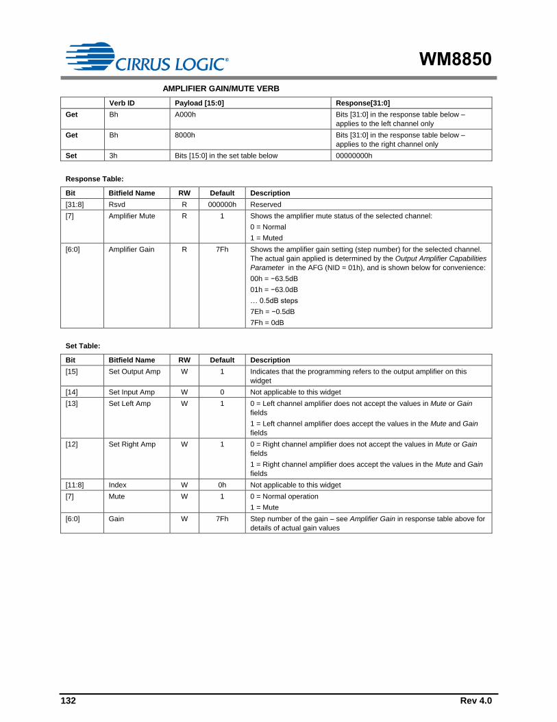
WM8850
132 Rev 4.0
AMPLIFIER GAIN/MUTE VERB
Verb ID Payload [15:0] Response[31:0]
Get Bh A000h Bits [31:0] in the response table below –
applies to the left channel only
Get Bh 8000h Bits [31:0] in the response table below –
applies to the right channel only
Set 3h Bits [15:0] in the set table below 00000000h
Response Table:
Bit Bitfield Name RW Default Description
[31:8] Rsvd R 000000h Reserved
[7] Amplifier Mute R 1 Shows the amplifier mute status of the selected channel:
0 = Normal
1 = Muted
[6:0] Amplifier Gain R 7Fh Shows the amplifier gain setting (step number) for the selected channel.
The actual gain applied is determined by the Output Amplifier Capabilities
Parameter in the AFG (NID = 01h), and is shown below for convenience:
00h = −63.5dB
01h = −63.0dB
… 0.5dB steps
7Eh = −0.5dB
7Fh = 0dB
Set Table:
Bit Bitfield Name RW Default Description
[15] Set Output Amp W 1 Indicates that the programming refers to the output amplifier on this
widget
[14] Set Input Amp W 0 Not applicable to this widget
[13] Set Left Amp W 1 0 = Left channel amplifier does not accept the values in Mute or Gain
fields
1 = Left channel amplifier does accept the values in the Mute and Gain
fields
[12] Set Right Amp W 1 0 = Right channel amplifier does not accept the values in Mute or Gain
fields
1 = Right channel amplifier does accept the values in the Mute and Gain
fields
[11:8] Index W 0h Not applicable to this widget
[7] Mute W 1 0 = Normal operation
1 = Mute
[6:0] Gain W 7Fh Step number of the gain – see Amplifier Gain in response table above for
details of actual gain values

WM8850
Rev 4.0 133
00h
01h
02h
03h
04h
05h
06h
07h
08h
09h
0Ah
0Bh
0Ch
0Dh
0Eh
0Fh
10h
11h
12h
13h
14h
15h
16h
17h
GET PARAMETER VERB
Verb ID Payload [7:0] Response[31:0]
Get F00h Parameter ID (PID) Parameter Value
Audio Widget Capabilities Parameter (PID = 09h)
Bit Bitfield Name RW Default Description
[31:24] Rsvd R 00h Reserved
[23:20] Type R 0h Indicates that this is an Audio Output Widget
[19:16] Delay R 0h Latency not reported
[15:12] Rsvd R 0h Reserved
[11] L-R Swap R 0 Left/Right swap capability not supported
[10] PowerCntrl R 1 Indicates that the Power State Verb is supported in this widget
[9] Digital R 0 Indicates that this widget is translating analogue data
[8] Conn List R 0 Indicates that a connection list is not present
[7] Unsol Capable R 1 Widget supports Unsolicited Responses
[6] ProcWidget R 0 Widget does not have processing capabilities
[5] Stripe R 0 Widget does not support striping
[4] Format Override R 1 Widget has a subset of the supported rates defined for the AFG
[3] Amp Parameter
Override
R 0 The AFG amplifier parameters are used for this widget
[2] Out Amp Present R 1 Output amplifier is present in this widget
[1] In Amp Present R 0 Input amplifier not present in this widget
[0] Stereo R 1 Indicates that this is a stereo widget
Supported Rates Parameter (PID = 0Ah)
Bit Bitfield Name RW Default Description
[31:21] Rsvd R 000h Reserved
[20] B32 R 1 DAC2 supports 32-bit audio format
[19] B24 R 1 DAC2 supports 24-bit audio format
[18] B20 R 1 DAC2 supports 20-bit audio format
[17] B16 R 1 DAC2 supports 16-bit audio format
[16] B8 R 0 DAC2 does not support 8-bit audio format
[15:12] Rsvd R 0h Reserved
[11] R12 R 0 DAC2 does not support 384 kHz sample rate
[10] R11 R 1 DAC2 supports 192 kHz sample rate
[9] R10 R 1 DAC2 supports 176.4 kHz sample rate
[8] R9 R 1 DAC2 supports 96 kHz sample rate
[7] R8 R 1 DAC2 supports 88.2 kHz sample rate
[6] R7 R 1 DAC2 supports 48 kHz sample rate
[5] R6 R 1 DAC2 supports 44.1 kHz sample rate
[4] R5 R 1 DAC2 supports 32 kHz sample rate
[3] R4 R 1 DAC2 supports 22.05 kHz sample rate
[2] R3 R 1 DAC2 supports 16 kHz sample rate
[1] R2 R 1 DAC2 supports 11.025 kHz sample rate
[0] R1 R 1 DAC2 supports 8 kHz sample rate
Supported Stream Formats Parameter (PID = 0Bh)
Bit Bitfield Name RW Default Description
[31:3] Rsvd R 00000000h Reserved
[2] AC3 R 0 DAC2 does not support Dolby AC3 formatted data
[1] Float32 R 1 DAC2 supports Float32 formatted data
[0] PCM R 1 DAC2 supports PCM formatted data

WM8850
134 Rev 4.0
Supported Power States Parameter (PID = 0Fh)
Bit Bitfield Name RW Default Description
[31:4] Rsvd R 0000000h Reserved
[3] D3Sup R 1 D3 power state supported
[2] D2Sup R 1 D2 power state supported
[1] D1sup R 1 D1 power state supported
[0] D0Sup R 1 D0 power state supported
POWER STATE VERB
Verb ID Payload [7:0] Response[31:0]
Get F05h 00h Bits [31:0] in the table below
Set 705h Bits [7:0] in the table below 00000000h
Bit Bitfield Name RW Default Description
[31:8] Rsvd R 000000h Reserved
[7:4] PS-Act R 3h Indicates the actual power state of the DAC2 node:
0h = D0
1h = D1
2h = D2
3h = D3
4h-Fh = Reserved
The power state of the DAC2 node is controlled by PS-Set below, however
the control may be superseded by the PS-Set of the AFG node.
[3:0] PS-Set RW 3h Sets the power state of the DAC2 node:
0h = D0
1h = D1
2h = D2
3h = D3
4h-Fh = Reserved
CONVERTER STREAM, CHANNEL VERB
Verb ID Payload [7:0] Response[31:0]
Get F06h 00h Bits [31:0] in the table below
Set 706h Bits [7:0] in the table below 00000000h
Bit Bitfield Name RW Default Description
[31:8] Rsvd R 000000h Reserved
[7:4] Stream RW 0h Stream ID used by this widget. Note that Stream ID = 0h is used to
indicate an unused stream, and converters will not transfer/receive link
data for streams with an ID of 0h.
[3:0] Channel RW 0h Lowest channel number used by this widget.
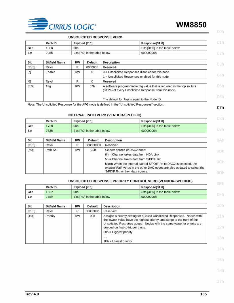
WM8850
Rev 4.0 135
00h
01h
02h
03h
04h
05h
06h
07h
08h
09h
0Ah
0Bh
0Ch
0Dh
0Eh
0Fh
10h
11h
12h
13h
14h
15h
16h
17h
UNSOLICITED RESPONSE VERB
Verb ID Payload [7:0] Response[31:0]
Get F08h 00h Bits [31:0] in the table below
Set 708h Bits [7:0] in the table below 00000000h
Bit Bitfield Name RW Default Description
[31:8] Rsvd R 000000h Reserved
[7] Enable RW 0 0 = Unsolicited Responses disabled for this node
1 = Unsolicited Responses enabled for this node
[6] Rsvd R 0 Reserved
[5:0] Tag RW 07h A software programmable tag value that is returned in the top six bits
(31:26) of every Unsolicited Response from this node.
The default for Tag is equal to the Node ID.
Note: The Unsolicited Response for the AFG node is defined in the “Unsolicited Responses” section.
INTERNAL PATH VERB (VENDOR-SPECIFIC)
Verb ID Payload [7:0] Response[31:0]
Get F73h 00h Bits [31:0] in the table below
Set 773h Bits [7:0] in the table below 00000000h
Bit Bitfield Name RW Default Description
[31:8] Rsvd R 00000000h Reserved
[7:0] Path Sel RW 00h Selects source of DAC2 node:
0h = Channel takes data from HDA Link
5h = Channel takes data from S/PDIF Rx
Note: When the internal path of S/PDIF Rx to DAC2 is selected, the
Internal Path verbs in the other DAC nodes are also updated to select the
S/PDIF Rx as their data source.
UNSOLICITED RESPONSE PRIORITY CONTROL VERB (VENDOR-SPECIFIC)
Verb ID Payload [7:0] Response[31:0]
Get F8Eh 00h Bits [31:0] in the table below
Set 78Eh Bits [7:0] in the table below 00000000h
Bit Bitfield Name RW Default Description
[31:5] Rsvd R 0000000h Reserved
[4:0] Priority RW 00h Assigns a priority setting for queued Unsolicited Responses. Nodes with
the lowest value have the highest priority, and so go to the front of the
Unsolicited Response queue. Nodes with the same value for priority are
queued on first-to-trigger basis.
00h = Highest priority
…
1Fh = Lowest priority

WM8850
136 Rev 4.0
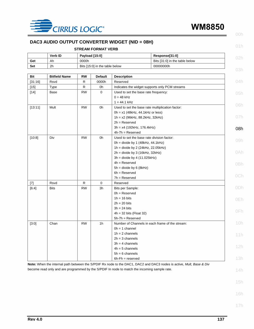
WM8850
Rev 4.0 137
00h
01h
02h
03h
04h
05h
06h
07h
08h
09h
0Ah
0Bh
0Ch
0Dh
0Eh
0Fh
10h
11h
12h
13h
14h
15h
16h
17h
DAC3 AUDIO OUTPUT CONVERTER WIDGET (NID = 08H)
STREAM FORMAT VERB
Verb ID Payload [15:0] Response[31:0]
Get Ah 0000h Bits [31:0] in the table below
Set 2h Bits [15:0] in the table below 00000000h
Bit Bitfield Name RW Default Description
[31:16] Rsvd R 0000h Reserved
[15] Type R 0h Indicates the widget supports only PCM streams
[14] Base RW 0 Used to set the base rate frequency:
0 = 48 kHz
1 = 44.1 kHz
[13:11] Mult RW 0h Used to set the base rate multiplication factor:
0h = x1 (48kHz, 44.1kHz or less)
1h = x2 (96kHz, 88.2kHz, 32kHz)
2h = Reserved
3h = x4 (192kHz, 176.4kHz)
4h-7h = Reserved
[10:8] Div RW 0h Used to set the base rate division factor:
0h = divide by 1 (48kHz, 44.1kHz)
1h = divide by 2 (24kHz, 22.05kHz)
2h = divide by 3 (16kHz, 32kHz)
3h = divide by 4 (11.025kHz)
4h = Reserved
5h = divide by 6 (8kHz)
6h = Reserved
7h = Reserved
[7] Rsvd R 0 Reserved
[6:4] Bits RW 3h Bits per Sample:
0h = Reserved
1h = 16 bits
2h = 20 bits
3h = 24 bits
4h = 32 bits (Float 32)
5h-7h = Reserved
[3:0] Chan RW 1h Number of Channels in each frame of the stream:
0h = 1 channel
1h = 2 channels
2h = 3 channels
3h = 4 channels
4h = 5 channels
5h = 6 channels
6h-Fh = reserved
Note: When the internal path between the S/PDIF Rx node to the DAC1, DAC2 and DAC3 nodes is active, Mult, Base & Div
become read only and are programmed by the S/PDIF In node to match the incoming sample rate.

WM8850
138 Rev 4.0
AMPLIFIER GAIN/MUTE VERB
Verb ID Payload [15:0] Response[31:0]
Get Bh A000h Bits [31:0] in the response table below –
applies to the left channel only
Get Bh 8000h Bits [31:0] in the response table below –
applies to the right channel only
Set 3h Bits [15:0] in the set table below 00000000h
Response Table:
Bit Bitfield Name RW Default Description
[31:8] Rsvd R 000000h Reserved
[7] Amplifier Mute R 1 Shows the amplifier mute status of the selected channel:
0 = Normal
1 = Muted
[6:0] Amplifier Gain R 7Fh Shows the amplifier gain setting (step number) for the selected channel.
The actual gain applied is determined by the Output Amplifier Capabilities
Parameter in the AFG (NID = 01h), and is shown below for convenience:
00h = −63.5dB
01h = −63.0dB
… 0.5dB steps
7Eh = −0.5dB
7Fh = 0dB
Set Table:
Bit Bitfield Name RW Default Description
[15] Set Output Amp W 1 Indicates that the programming refers to the output amplifier on this
widget
[14] Set Input Amp W 0 Not applicable to this widget
[13] Set Left Amp W 1 0 = Left channel amplifier does not accept the values in Mute or Gain
fields
1 = Left channel amplifier accepts the values in the Mute and Gain fields
[12] Set Right Amp W 1 0 = Right channel amplifier does not accept the values in Mute or Gain
fields
1 = Right channel amplifier accepts the values in the Mute and Gain
fields
[11:8] Index W 0h Not applicable to this widget
[7] Mute W 1 0 = Normal operation
1 = Mute
[6:0] Gain W 7Fh Step number of the gain – see Amplifier Gain in response table above for
details of actual gain values

WM8850
Rev 4.0 139
00h
01h
02h
03h
04h
05h
06h
07h
08h
09h
0Ah
0Bh
0Ch
0Dh
0Eh
0Fh
10h
11h
12h
13h
14h
15h
16h
17h
GET PARAMETER VERB
Verb ID Payload [7:0] Response[31:0]
Get F00h Parameter ID (PID) Parameter Value
Audio Widget Capabilities Parameter (PID = 09h)
Bit Bitfield Name RW Default Description
[31:24] Rsvd R 00h Reserved
[23:20] Type R 0h Indicates that this is an Audio Output Widget
[19:16] Delay R 0h Latency not reported
[15:12] Rsvd R 0h Reserved
[11] L-R Swap R 0 Left/Right swap capability not supported
[10] PowerCntrl R 1 Indicates that the Power State Verb is supported in this widget
[9] Digital R 0 Indicates that this widget is translating analogue data
[8] Conn List R 0 Indicates that a connection list is not present
[7] Unsol Capable R 1 Widget supports Unsolicited Responses
[6] ProcWidget R 0 Widget does not have processing capabilities
[5] Stripe R 0 Widget does not support striping
[4] Format Override R 1 Widget has a subset of the supported rates defined for the AFG
[3] Amp Parameter
Override
R 0 The AFG amplifier parameters are used for this widget
[2] Out Amp Present R 1 Output amplifier is present in this widget
[1] In Amp Present R 0 Input amplifier not present in this widget
[0] Stereo R 1 Indicates that this is a stereo widget
Supported Rates Parameter (PID = 0Ah)
Bit Bitfield Name RW Default Description
[31:21] Rsvd R 000h Reserved
[20] B32 R 1 DAC3 supports 32-bit audio format
[19] B24 R 1 DAC3 supports 24-bit audio format
[18] B20 R 1 DAC3 supports 20-bit audio format
[17] B16 R 1 DAC3 supports 16-bit audio format
[16] B8 R 0 DAC3 does not support 8-bit audio format
[15:12] Rsvd R 0h Reserved
[11] R12 R 0 DAC3 does not support 384 kHz sample rate
[10] R11 R 1 DAC3 supports 192 kHz sample rate
[9] R10 R 1 DAC3 supports 176.4 kHz sample rate
[8] R9 R 1 DAC3 supports 96 kHz sample rate
[7] R8 R 1 DAC3 supports 88.2 kHz sample rate
[6] R7 R 1 DAC3 supports 48 kHz sample rate
[5] R6 R 1 DAC3 supports 44.1 kHz sample rate
[4] R5 R 1 DAC3 supports 32 kHz sample rate
[3] R4 R 1 DAC3 supports 22.05 kHz sample rate
[2] R3 R 1 DAC3 supports 16 kHz sample rate
[1] R2 R 1 DAC3 supports 11.025 kHz sample rate
[0] R1 R 1 DAC3 supports 8 kHz sample rate
Supported Stream Formats Parameter (PID = 0Bh)
Bit Bitfield Name RW Default Description
[31:3] Rsvd R 00000000h Reserved
[2] AC3 R 0 DAC3 does not support Dolby AC3 formatted data
[1] Float32 R 1 DAC3 supports Float32 formatted data
[0] PCM R 1 DAC3 supports PCM formatted data

WM8850
140 Rev 4.0
Supported Power States Parameter (PID = 0Fh)
Bit Bitfield Name RW Default Description
[31:4] Rsvd R 0000000h Reserved
[3] D3Sup R 1 D3 power state supported
[2] D2Sup R 1 D2 power state supported
[1] D1sup R 1 D1 power state supported
[0] D0Sup R 1 D0 power state supported
POWER STATE VERB
Verb ID Payload [7:0] Response[31:0]
Get F05h 00h Bits [31:0] in the table below
Set 705h Bits [7:0] in the table below 00000000h
Bit Bitfield Name RW Default Description
[31:8] Rsvd R 000000h Reserved
[7:4] PS-Act R 3h Indicates the actual power state of the DAC3 node:
0h = D0
1h = D1
2h = D2
3h = D3
4h-Fh = Reserved
The power state of the DAC3 node is controlled by PS-Set below, however
the control may be superseded by the PS-Set of the AFG node.
[3:0] PS-Set RW 3h Sets the power state of the DAC3 node:
0h = D0
1h = D1
2h = D2
3h = D3
4h-Fh = Reserved
CONVERTER STREAM, CHANNEL VERB
Verb ID Payload [7:0] Response[31:0]
Get F06h 00h Bits [31:0] in the table below
Set 706h Bits [7:0] in the table below 00000000h
Bit Bitfield Name RW Default Description
[31:8] Rsvd R 000000h Reserved
[7:4] Stream RW 0h Stream ID used by this widget. Note that Stream ID = 0h is used to
indicate an unused stream, and converters will not transfer/receive link
data for streams with an ID of 0h.
[3:0] Channel RW 0h Lowest channel number used by this widget.

WM8850
Rev 4.0 141
00h
01h
02h
03h
04h
05h
06h
07h
08h
09h
0Ah
0Bh
0Ch
0Dh
0Eh
0Fh
10h
11h
12h
13h
14h
15h
16h
17h
UNSOLICITED RESPONSE VERB
Verb ID Payload [7:0] Response[31:0]
Get F08h 00h Bits [31:0] in the table below
Set 708h Bits [7:0] in the table below 00000000h
Bit Bitfield Name RW Default Description
[31:8] Rsvd R 000000h Reserved
[7] Enable RW 0 0 = Unsolicited Responses disabled for this node
1 = Unsolicited Responses enabled for this node
[6] Rsvd R 0 Reserved
[5:0] Tag RW 08h A software programmable tag value that is returned in the top six bits
(31:26) of every Unsolicited Response from this node.
The default for Tag is equal to the Node ID.
Note: The Unsolicited Response for the AFG node is defined in the “Unsolicited Responses” section.
INTERNAL PATH VERB (VENDOR-SPECIFIC)
Verb ID Payload [7:0] Response[31:0]
Get F73h 00h Bits [31:0] in the table below
Set 773h Bits [7:0] in the table below 00000000h
Bit Bitfield Name RW Default Description
[31:8] Rsvd R 00000000h Reserved
[7:0] Path Sel RW 00h Selects source of DAC3 node:
0h = Channel takes data from HDA Link
5h = Channel takes data from S/PDIF Rx
Note: When the internal path of S/PDIF Rx to DAC3 is selected, the
Internal Path verbs in the other DAC nodes are also updated to select the
S/PDIF Rx as their data source.
UNSOLICITED RESPONSE PRIORITY CONTROL VERB (VENDOR-SPECIFIC)
Verb ID Payload [7:0] Response[31:0]
Get F8Eh 00h Bits [31:0] in the table below
Set 78Eh Bits [7:0] in the table below 00000000h
Bit Bitfield Name RW Default Description
[31:5] Rsvd R 0000000h Reserved
[4:0] Priority RW 00h Assigns a priority setting for queued Unsolicited Responses. Nodes with
the lowest value have the highest priority, and so go to the front of the
Unsolicited Response queue. Nodes with the same value for priority are
queued on first-to-trigger basis.
00h = Highest priority
…
1Fh = Lowest priority

WM8850
142 Rev 4.0

WM8850
Rev 4.0 143
00h
01h
02h
03h
04h
05h
06h
07h
08h
09h
0Ah
0Bh
0Ch
0Dh
0Eh
0Fh
10h
11h
12h
13h
14h
15h
16h
17h
MIC1 MUX SELECTOR WIDGET (NID = 09H)
GET PARAMETER VERB
Verb ID Payload [7:0] Response[31:0]
Get F00h Parameter ID (PID) Parameter Value
Audio Widget Capabilities Parameter (PID = 09h)
Bit Bitfield Name RW Default Description
[31:24] Rsvd R 00h Reserved
[23:20] Type R 3h Indicates that this is an Audio Selector Widget
[19:16] Delay R 0h Latency not reported
[15:12] Rsvd R 0h Reserved
[11] L-R Swap R 0 Left/Right swap capability not supported
[10] PowerCntrl R 0 Indicates that the Power State Verb is not supported in this widget
[9] Digital R 0 Indicates that this widget is translating analogue data
[8] Conn List R 1 Indicates that a connection list is present
[7] Unsol Capable R 0 Widget supports Unsolicited Responses
[6] ProcWidget R 0 Widget does not have processing capabilities
[5] Stripe R 0 Widget does not support striping
[4] Format Override R 0 Widget does not override the format defined for the AFG
[3] Amp Parameter
Override
R 0 Not applicable as this widget does not have amplifier capabilities
[2] Out Amp Present R 0 Output amplifier is not present in this widget
[1] In Amp Present R 0 Input amplifier not present in this widget
[0] Stereo R 1 Indicates that this is a stereo widget
Connection List Length Parameter (PID = 0Eh)
Bit Bitfield Name RW Default Description
[31:8] Rsvd R 000000h Reserved
[7] Long Form R 0 Indicates that the connection list items are in short form
[6:0] Connection List
Length
R 02h Indicates that there is 2 NID entries in the connection list
CONNECTION SELECT CONTROL VERB
Verb ID Payload [7:0] Response[31:0]
Get F01h 00h Bits [31:0] in the table below
Set 701h Bits [7:0] in the table below 00000000h
Bit Bitfield Name RW Default Description
[31:8] Rsvd R 000000h Reserved
[7:0] Connection
Index
RW 00h Connection index currently set:
00h = Connection list entry 0
01h = Connection list entry 1
02h-FFh = Reserved
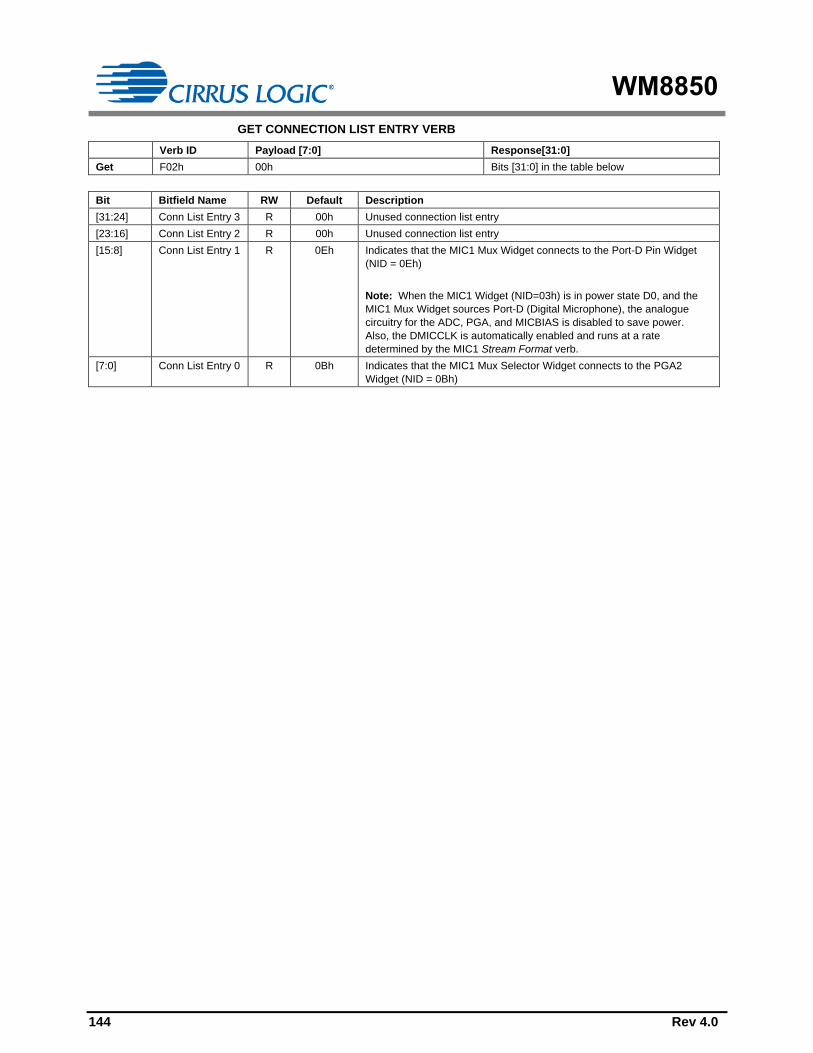
WM8850
144 Rev 4.0
GET CONNECTION LIST ENTRY VERB
Verb ID Payload [7:0] Response[31:0]
Get F02h 00h Bits [31:0] in the table below
Bit Bitfield Name RW Default Description
[31:24] Conn List Entry 3 R 00h Unused connection list entry
[23:16] Conn List Entry 2 R 00h Unused connection list entry
[15:8] Conn List Entry 1 R 0Eh Indicates that the MIC1 Mux Widget connects to the Port-D Pin Widget
(NID = 0Eh)
Note: When the MIC1 Widget (NID=03h) is in power state D0, and the
MIC1 Mux Widget sources Port-D (Digital Microphone), the analogue
circuitry for the ADC, PGA, and MICBIAS is disabled to save power.
Also, the DMICCLK is automatically enabled and runs at a rate
determined by the MIC1 Stream Format verb.
[7:0] Conn List Entry 0 R 0Bh Indicates that the MIC1 Mux Selector Widget connects to the PGA2
Widget (NID = 0Bh)

WM8850
Rev 4.0 145
00h
01h
02h
03h
04h
05h
06h
07h
08h
09h
0Ah
0Bh
0Ch
0Dh
0Eh
0Fh
10h
11h
12h
13h
14h
15h
16h
17h
PGA1 SELECTOR WIDGET (NID = 0AH)
AMPLIFIER GAIN/MUTE VERB
Verb ID Payload [15:0] Response[31:0]
Get Bh A000h Bits [31:0] in the response table below –
applies to the left channel only
Get Bh 8000h Bits [31:0] in the response table below –
applies to the right channel only
Set 3h Bits [15:0] in the set table below 00000000h
Response Table:
Bit Bitfield Name RW Default Description
[31:8] Rsvd R 000000h Reserved
[7] Amplifier Mute R 1 Shows the amplifier mute status of the selected channel:
0 = Normal
1 = Muted
[6:0] Amplifier Gain R 18h Shows the amplifier gain setting (step number) for the selected channel.
The actual gain applied is determined by the Output Amplifier Capabilities
Parameter, and is shown below for convenience:
00h = −12dB
01h = −11.5dB
… 0.5dB steps
2Fh = +11.5dB
30h = +12dB
Note: If the BTL register in the Port-E Pin Widget (NID=0Ch) EAPD/BTL
Verb is set to 0, the input is single-ended and the actual gain setting
applied has an offset of −3dB from the setting configured by the Gain
register.
Set Table:
Bit Bitfield Name RW Default Description
[15] Set Output Amp W 1 Indicates that the programming refers to the output amplifier on this
widget
[14] Set Input Amp W 0 Not applicable to this widget
[13] Set Left Amp W 1 0 = Left channel amplifier does not accept the values in Mute or Gain
fields
1 = Left channel amplifier does accept the values in the Mute and Gain
fields
[12] Set Right Amp W 1 0 = Right channel amplifier does not accept the values in Mute or Gain
fields
1 = Right channel amplifier does accept the values in the Mute and Gain
fields
[11:8] Index W 0h Not applicable to this widget
[7] Mute W 1 0 = Normal operation
1 = Mute
Note: When mute is applied to a channel, the data value is overwritten
with all zeros.
[6:0] Gain W 18h Step number of the gain – see Amplifier Gain in response table above for
details of actual gain values

WM8850
146 Rev 4.0
GET PARAMETER VERB
Verb ID Payload [7:0] Response[31:0]
Get F00h Parameter ID (PID) Parameter Value
Audio Widget Capabilities Parameter (PID = 09h)
Bit Bitfield Name RW Default Description
[31:24] Rsvd R 00h Reserved
[23:20] Type R 3h Indicates that this is an Audio Selector Widget
[19:16] Delay R 0h Latency not reported
[15:12] Rsvd R 0h Reserved
[11] L-R Swap R 0 Left/Right swap capability not supported
[10] PowerCntrl R 0 Indicates that the Power State Verb is not supported in this widget
[9] Digital R 0 Indicates that this widget is translating analogue data
[8] Conn List R 1 Indicates that a connection list is present
[7] Unsol Capable R 0 Widget supports Unsolicited Responses
[6] ProcWidget R 0 Widget does not have processing capabilities
[5] Stripe R 0 Widget does not support striping
[4] Format Override R 0 Widget does not override the format defined for the AFG
[3] Amp Parameter
Override
R 1 The AFG amplifier parameters are overridden for this node
[2] Out Amp Present R 1 Output amplifier is present in this widget
[1] In Amp Present R 0 Input amplifier not present in this widget
[0] Stereo R 1 Indicates that this is a stereo widget
Connection List Length Parameter (PID = 0Eh)
Bit Bitfield Name RW Default Description
[31:8] Rsvd R 000000h Reserved
[7] Long Form R 0 Indicates that the connection list items are in short form
[6:0] Connection List
Length
R 01h Indicates that there is 1 NID entries in the connection list
Output Amplifier Capabilities Response Format (PID = 12h)
Bit Bitfield Name RW Default Description
[31] Mute Capable R 1 PGA1 is capable of muting
[30:23] Rsvd R 0000h Reserved
[22:16] Step Size R 01h Gain step size is 0.5dB
[15] Rsvd R 0 Reserved
[14:8] Num Steps R 30h Number of steps in gain range is 49 (−12dB to +12dB)
[7] Rsvd R 0 Reserved
[6:0] Offset R 18h The step number that 0dB corresponds to is 18h
GET CONNECTION LIST ENTRY VERB
Verb ID Payload [7:0] Response[31:0]
Get F02h 00h Bits [31:0] in the table below
Bit Bitfield Name RW Default Description
[31:24] Conn List Entry 3 R 00h Unused connection list entry
[23:16] Conn List Entry 2 R 00h Unused connection list entry
[15:8] Conn List Entry 1 R 00h Unused connection list entry
[7:0] Conn List Entry 0 R 0Ch Indicates that the PGA1 Widget connects to the Port-E Pin Widget (NID =
0Ch)

WM8850
Rev 4.0 147
00h
01h
02h
03h
04h
05h
06h
07h
08h
09h
0Ah
0Bh
0Ch
0Dh
0Eh
0Fh
10h
11h
12h
13h
14h
15h
16h
17h
PGA CONTROL VERB (VENDOR-SPECIFIC)
Verb ID Payload [7:0] Response[31:0]
Get FB2h 00h Bits [31:0] in the table below
Set1 7B2h Bits [7:0] in the table below 00000000h
Set2 7B3h Bits [15:0] in the table below 00000000h
Bit Bitfield Name RW Default Description
[31:14] Rsvd R 00000h Reserved
[13:0] Terminal Count RW 1FFFh Set the period of the zero detect timeout clock:
0000h = Timeout disabled
0001h to 03FFh = Reserved
0400h = 1025 x 20.833µs (21.3ms)
0401h = 1026 x 20.833µs (21.4ms)
…
1FFFh = 8192 × 20.833µs (171ms)
…
3FFFh = 16384 × 20.833µs (341ms)
Note: The timeout clock uses the SYNC signal from the HDA interface,
so the absolute value of the timeout period will depend on the absolute
accuracy of the SYNC signal.

WM8850
148 Rev 4.0

WM8850
Rev 4.0 149
00h
01h
02h
03h
04h
05h
06h
07h
08h
09h
0Ah
0Bh
0Ch
0Dh
0Eh
0Fh
10h
11h
12h
13h
14h
15h
16h
17h
PGA2 SELECTOR WIDGET (NID = 0BH)
AMPLIFIER GAIN/MUTE VERB
Verb ID Payload [15:0] Response[31:0]
Get Bh A000h Bits [31:0] in the response table below –
applies to the left channel only
Get Bh 8000h Bits [31:0] in the response table below –
applies to the right channel only
Set 3h Bits [15:0] in the set table below 00000000h
Response Table:
Bit Bitfield Name RW Default Description
[31:8] Rsvd R 000000h Reserved
[7] Amplifier Mute R 1 Shows the amplifier mute status of the selected channel:
0 = Normal
1 = Muted
[6:0] Amplifier Gain R 18h Shows the amplifier gain setting (step number) for the selected channel.
The actual gain applied is determined by the Output Amplifier Capabilities
Parameter, and is shown below for convenience:
00h = −12dB
01h = −11.5dB
… 0.5dB steps
2Fh = +11.5dB
30h = +12dB
Set Table:
Bit Bitfield Name RW Default Description
[15] Set Output Amp W 1 Indicates that the programming refers to the output amplifier on this
widget
[14] Set Input Amp W 0 Not applicable to this widget
[13] Set Left Amp W 1 0 = Left channel amplifier does not accept the values in Mute or Gain
fields
1 = Left channel amplifier does accept the values in the Mute and Gain
fields
[12] Set Right Amp W 1 0 = Right channel amplifier does not accept the values in Mute or Gain
fields
1 = Right channel amplifier does accept the values in the Mute and Gain
fields
[11:8] Index W 0h Not applicable to this widget
[7] Mute W 1 0 = Normal operation
1 = Mute
Note: When mute is applied to a channel, the data value is overwritten
with all zeros.
[6:0] Gain W 18h Step number of the gain – see Amplifier Gain in response table above for
details of actual gain values

WM8850
150 Rev 4.0
GET PARAMETER VERB
Verb ID Payload [7:0] Response[31:0]
Get F00h Parameter ID (PID) Parameter Value
Audio Widget Capabilities Parameter (PID = 09h)
Bit Bitfield Name RW Default Description
[31:24] Rsvd R 00h Reserved
[23:20] Type R 3h Indicates that this is an Audio Selector Widget
[19:16] Delay R 0h Latency not reported
[15:12] Rsvd R 0h Reserved
[11] L-R Swap R 0 Left/Right swap capability not supported
[10] PowerCntrl R 0 Indicates that the Power State Verb is not supported in this widget
[9] Digital R 0 Indicates that this widget is translating analogue data
[8] Conn List R 1 Indicates that a connection list is present
[7] Unsol Capable R 0 Widget supports Unsolicited Responses
[6] ProcWidget R 0 Widget does not have processing capabilities
[5] Stripe R 0 Widget does not support striping
[4] Format Override R 0 Widget does not override the format defined for the AFG
[3] Amp Parameter
Override
R 1 The AFG amplifier parameters are overridden for this node
[2] Out Amp Present R 1 Output amplifier is present in this widget
[1] In Amp Present R 0 Input amplifier not present in this widget
[0] Stereo R 1 Indicates that this is a stereo widget
Connection List Length Parameter (PID = 0Eh)
Bit Bitfield Name RW Default Description
[31:8] Rsvd R 000000h Reserved
[7] Long Form R 0 Indicates that the connection list items are in short form
[6:0] Connection List
Length
R 01h Indicates that there is 1 NID entry in the connection list
Output Amplifier Capabilities Response Format (PID = 12h)
Bit Bitfield Name RW Default Description
[31] Mute Capable R 1 PGA2 is capable of muting
[30:23] Rsvd R 0000h Reserved
[22:16] Step Size R 01h Gain step size is 0.5dB
[15] Rsvd R 0 Reserved
[14:8] Num Steps R 30h Number of steps in gain range is 49 (−12dB to +12dB)
[7] Rsvd R 0 Reserved
[6:0] Offset R 18h The step number that 0dB corresponds to is 18h
GET CONNECTION LIST ENTRY VERB
Verb ID Payload [7:0] Response[31:0]
Get F02h 00h Bits [31:0] in the table below
Bit Bitfield Name RW Default Description
[31:24] Conn List Entry 3 R 00h Unused connection list entry
[23:16] Conn List Entry 2 R 00h Unused connection list entry
[15:8] Conn List Entry 1 R 00h Unused connection list entry
[7:0] Conn List Entry 0 R 0Dh Indicates that the PGA2 Widget connects to the Port-B Pin Widget (NID =
0Dh)

WM8850
Rev 4.0 151
00h
01h
02h
03h
04h
05h
06h
07h
08h
09h
0Ah
0Bh
0Ch
0Dh
0Eh
0Fh
10h
11h
12h
13h
14h
15h
16h
17h
PGA CONTROL VERB (VENDOR-SPECIFIC
Verb ID Payload [7:0] Response[31:0]
Get FB2h 00h Bits [31:0] in the table below
Set1 7B2h Bits [7:0] in the table below 00000000h
Set2 7B3h Bits [15:0] in the table below 00000000h
Bit Bitfield Name RW Default Description
[31:14] Rsvd R 00000h Reserved
[13:0] Terminal Count RW 1FFFh Set the period of the zero detect timeout clock:
0000h = Timeout disabled
0001h to 03FFh = Reserved
0400h = 1025 x 20.833µs (21.3ms)
0401h = 1026 x 20.833µs (21.4ms)
…
1FFFh = 8192 × 20.833µs (171ms)
…
3FFFh = 16384 × 20.833µs (341ms)
Note: The timeout clock uses the SYNC signal from the HDA interface,
so the absolute value of the timeout period will depend on the absolute
accuracy of the SYNC signal.

WM8850
152 Rev 4.0
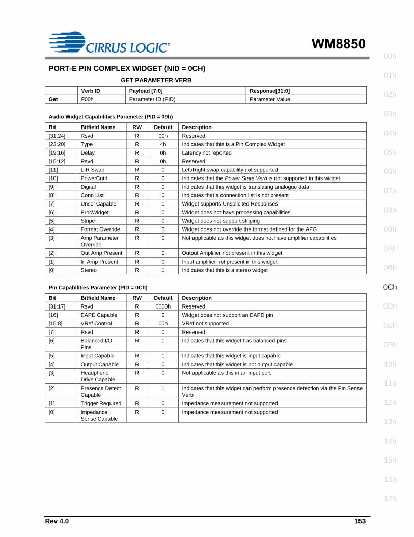
WM8850
Rev 4.0 153
00h
01h
02h
03h
04h
05h
06h
07h
08h
09h
0Ah
0Bh
0Ch
0Dh
0Eh
0Fh
10h
11h
12h
13h
14h
15h
16h
17h
PORT-E PIN COMPLEX WIDGET (NID = 0CH)
GET PARAMETER VERB
Verb ID Payload [7:0] Response[31:0]
Get F00h Parameter ID (PID) Parameter Value
Audio Widget Capabilities Parameter (PID = 09h)
Bit Bitfield Name RW Default Description
[31:24] Rsvd R 00h Reserved
[23:20] Type R 4h Indicates that this is a Pin Complex Widget
[19:16] Delay R 0h Latency not reported
[15:12] Rsvd R 0h Reserved
[11] L-R Swap R 0 Left/Right swap capability not supported
[10] PowerCntrl R 0 Indicates that the Power State Verb is not supported in this widget
[9] Digital R 0 Indicates that this widget is translating analogue data
[8] Conn List R 0 Indicates that a connection list is not present
[7] Unsol Capable R 1 Widget supports Unsolicited Responses
[6] ProcWidget R 0 Widget does not have processing capabilities
[5] Stripe R 0 Widget does not support striping
[4] Format Override R 0 Widget does not override the format defined for the AFG
[3] Amp Parameter
Override
R 0 Not applicable as this widget does not have amplifier capabilities
[2] Out Amp Present R 0 Output Amplifier not present in this widget
[1] In Amp Present R 0 Input amplifier not present in this widget
[0] Stereo R 1 Indicates that this is a stereo widget
Pin Capabilities Parameter (PID = 0Ch)
Bit Bitfield Name RW Default Description
[31:17] Rsvd R 0000h Reserved
[16] EAPD Capable R 0 Widget does not support an EAPD pin
[15:8] VRef Control R 00h VRef not supported
[7] Rsvd R 0 Reserved
[6] Balanced I/O
Pins
R 1 Indicates that this widget has balanced pins
[5] Input Capable R 1 Indicates that this widget is input capable
[4] Output Capable R 0 Indicates that this widget is not output capable
[3] Headphone
Drive Capable
R 0 Not applicable as this in an input port
[2] Presence Detect
Capable
R 1 Indicates that this widget can perform presence detection via the Pin Sense
Verb
[1] Trigger Required R 0 Impedance measurement not supported
[0] Impedance
Sense Capable
R 0 Impedance measurement not supported
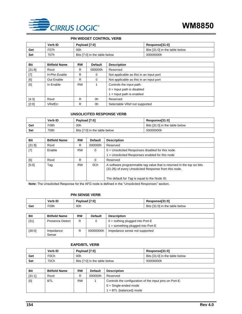
WM8850
154 Rev 4.0
PIN WIDGET CONTROL VERB
Verb ID Payload [7:0] Response[31:0]
Get F07h 00h Bits [31:0] in the table below
Set 707h Bits [7:0] in the table below 00000000h
Bit Bitfield Name RW Default Description
[31:8] Rsvd R 000000h Reserved
[7] H-Phn Enable R 0 Not applicable as this in an input port
[6] Out Enable R 0 Not applicable as this in an input port
[5] In Enable RW 1 Controls the input path:
0 = Input path is disabled
1 = Input path is enabled
[4:3] Rsvd R 0h Reserved
[2:0] VRefEn R 0h Selectable VRef not supported
UNSOLICITED RESPONSE VERB
Verb ID Payload [7:0] Response[31:0]
Get F08h 00h Bits [31:0] in the table below
Set 708h Bits [7:0] in the table below 00000000h
Bit Bitfield Name RW Default Description
[31:8] Rsvd R 000000h Reserved
[7] Enable RW 0 0 = Unsolicited Responses disabled for this node
1 = Unsolicited Responses enabled for this node
[6] Rsvd R 0 Reserved
[5:0] Tag RW 0Ch A software programmable tag value that is returned in the top six bits
(31:26) of every Unsolicited Response from this node.
The default for Tag is equal to the Node ID.
Note: The Unsolicited Response for the AFG node is defined in the “Unsolicited Responses” section.
PIN SENSE VERB
Verb ID Payload [7:0] Response[31:0]
Get F09h 00h Bits [31:0] in the table below
Bit Bitfield Name RW Default Description
[31] Presence Detect R 0 0 = nothing plugged into Port-E
1 = something plugged into Port-E
[30:0] Impedance
Sense
R 00000000h Impedance sense not supported
EAPD/BTL VERB
Verb ID Payload [7:0] Response[31:0]
Get F0Ch 00h Bits [31:0] in the table below
Set 70Ch Bits [7:0] in the table below 00000000h
Bit Bitfield Name RW Default Description
[31:1] Rsvd R 000000h Reserved
[0] BTL RW 1 Controls the configuration of the input pins on Port-E:
0 = Single-ended mode
1 = BTL (balanced) mode
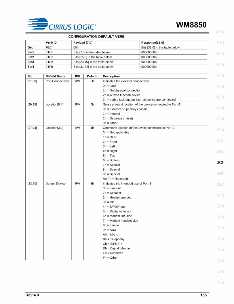
WM8850
Rev 4.0 155
00h
01h
02h
03h
04h
05h
06h
07h
08h
09h
0Ah
0Bh
0Ch
0Dh
0Eh
0Fh
10h
11h
12h
13h
14h
15h
16h
17h
CONFIGURATION DEFAULT VERB
Verb ID Payload [7:0] Response[31:0]
Get F1Ch 00h Bits [31:0] in the table below
Set1 71Ch Bits [7:0] in the table below 00000000h
Set2 71Dh Bits [15:8] in the table below 00000000h
Set3 71Eh Bits [23:16] in the table below 00000000h
Set4 71Fh Bits [31:24] in the table below 00000000h
Bit Bitfield Name RW Default Description
[31:30] Port Connectivity RW 0h Indicates the external connectivity:
0h = Jack
1h = No physical connection
2h = A fixed function device
3h = both a jack and an internal device are connected
[29:28] Location[5:4] RW 0h Gross physical location of the device connected to Port-E:
0h = External on primary chassis
1h = Internal
2h = Separate chassis
3h = Other
[27:24] Location[3:0] RW 1h Geometric location of the device connected to Port-E:
0h = Not applicable
1h = Rear
2h = Front
3h = Left
4h = Right
5h = Top
6h = Bottom
7h = Special
8h = Special
9h = Special
Ah-Fh = Reserved
[23:20] Default Device RW 8h Indicates the intended use of Port-E:
0h = Line out
1h = Speaker
2h = Headphone out
3h = CD
4h = S/PDIF out
5h = Digital other out
6h = Modem line side
7h = Modem handset side
8h = Line in
9h = AUX
Ah = Mic in
Bh = Telephony
Ch = S/PDIF in
Dh = Digital other in
Eh = Reserved
Fh = Other
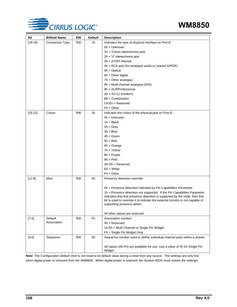
WM8850
156 Rev 4.0
Bit Bitfield Name RW Default Description
[19:16] Connection Type RW 1h Indicates the type of physical interface on Port-E:
0h = Unknown
1h = 3.5mm stereo/mono jack
2h = ¼” stereo/mono jack
3h = ATAPI internal
4h = RCA jack (for analogue audio or coaxial S/PDIF)
5h = Optical
6h = Other digital
7h = Other analogue
8h = Multi-channel analogue (DIN)
9h = XLR/Professional
Ah = RJ-11 (modem)
Bh = Combination
Ch-Eh = Reserved
Fh = Other
[15:12] Colour RW 3h Indicates the colour of the physical jack on Port-E:
0h = Unknown
1h = Black
2h = Grey
3h = Blue
4h = Green
5h = Red
6h = Orange
7h = Yellow
8h = Purple
9h = Pink
Ah-Dh = Reserved
Eh = White
Fh = Other
[11:8] Misc RW 0h Presence detection override:
0h = Presence detection indicated by Pin Capabilities Parameter
1h = Presence detection not supported. If the Pin Capabilities Parameter
indicates that that presence detection is supported by the node, then this
bit is used to override it to indicate the external circuitry is not capable of
supporting presence detect
All other values are reserved
[7:4] Default
Association
RW Fh Association number:
0h = Reserved
1h-Eh = Multi Channel or Single Pin Widget
Fh = Single Pin Widget Only
[3:0] Sequence RW 0h Sequence number used to define individual channel pairs within a stream.
All values (0h-Fh) are available for use. Use a value of 0h for Single Pin
Widget.
Note: The Configuration Default Verb is not reset to its default value during a reset from any source. The settings are only lost
when digital power is removed from the WM8850. When digital power is restored, the System BIOS must restore the settings.
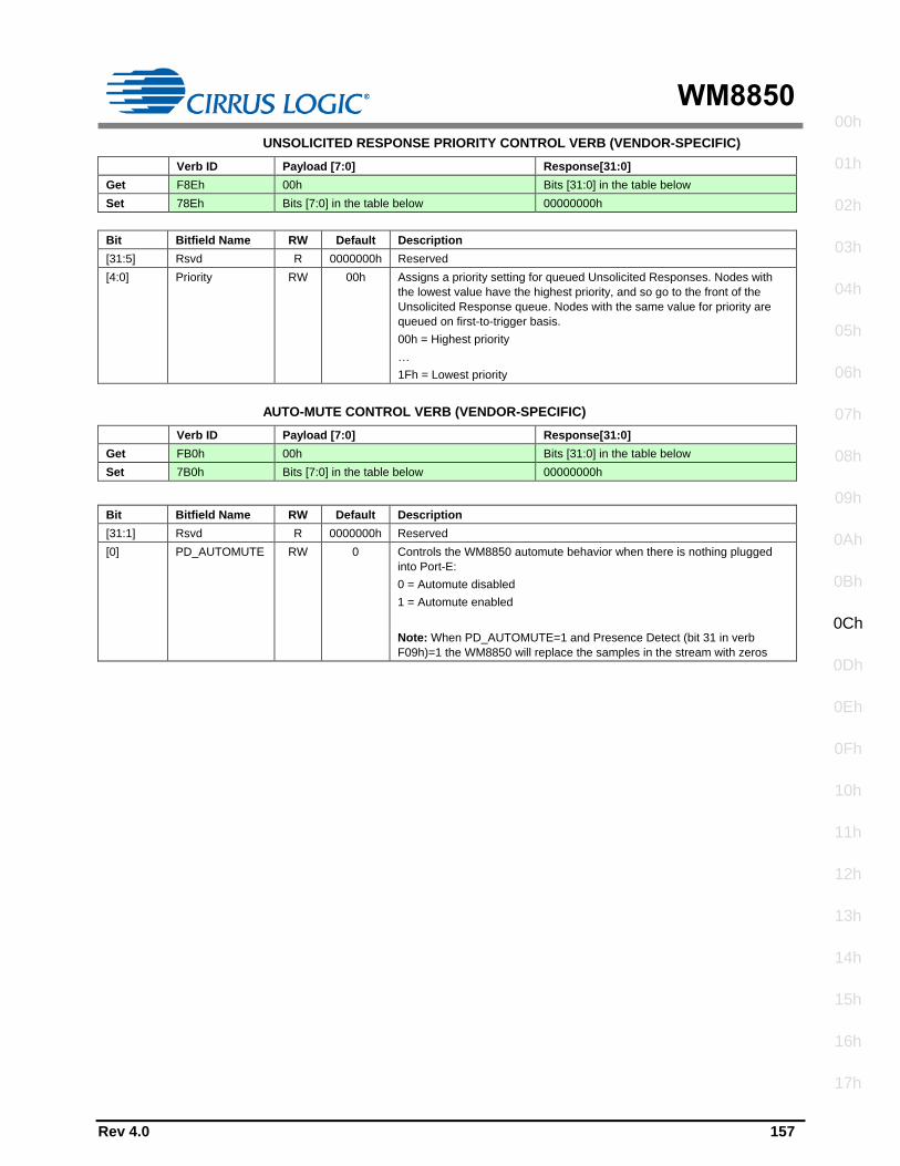
WM8850
Rev 4.0 157
00h
01h
02h
03h
04h
05h
06h
07h
08h
09h
0Ah
0Bh
0Ch
0Dh
0Eh
0Fh
10h
11h
12h
13h
14h
15h
16h
17h
UNSOLICITED RESPONSE PRIORITY CONTROL VERB (VENDOR-SPECIFIC)
Verb ID Payload [7:0] Response[31:0]
Get F8Eh 00h Bits [31:0] in the table below
Set 78Eh Bits [7:0] in the table below 00000000h
Bit Bitfield Name RW Default Description
[31:5] Rsvd R 0000000h Reserved
[4:0] Priority RW 00h Assigns a priority setting for queued Unsolicited Responses. Nodes with
the lowest value have the highest priority, and so go to the front of the
Unsolicited Response queue. Nodes with the same value for priority are
queued on first-to-trigger basis.
00h = Highest priority
…
1Fh = Lowest priority
AUTO-MUTE CONTROL VERB (VENDOR-SPECIFIC)
Verb ID Payload [7:0] Response[31:0]
Get FB0h 00h Bits [31:0] in the table below
Set 7B0h Bits [7:0] in the table below 00000000h
Bit Bitfield Name RW Default Description
[31:1] Rsvd R 0000000h Reserved
[0] PD_AUTOMUTE RW 0 Controls the WM8850 automute behavior when there is nothing plugged
into Port-E:
0 = Automute disabled
1 = Automute enabled
Note: When PD_AUTOMUTE=1 and Presence Detect (bit 31 in verb
F09h)=1 the WM8850 will replace the samples in the stream with zeros

WM8850
158 Rev 4.0

WM8850
Rev 4.0 159
00h
01h
02h
03h
04h
05h
06h
07h
08h
09h
0Ah
0Bh
0Ch
0Dh
0Eh
0Fh
10h
11h
12h
13h
14h
15h
16h
17h
PORT-B PIN COMPLEX WIDGET (NID = 0DH)
AMPLIFIER GAIN/MUTE VERB
Verb ID Payload [15:0] Response[31:0]
Get Bh 2000h Bits [31:0] in the response table below –
applies to the left channel only
Get Bh 0000h Bits [31:0] in the response table below –
applies to the right channel only
Set 3h Bits [15:0] in the set table below 00000000h
Response Table:
Bit Bitfield Name RW Default Description
[31:8] Rsvd R 000000h Reserved
[7] Amplifier Mute R 0 Mute not supported
[6:0] Amplifier Gain R 00h Shows the amplifier gain setting (step number) for the selected channel.
The actual gain applied is determined by the Input Amplifier Capabilities
Parameter in the AFG (NID = 01h), and is shown below for convenience:
00h = 0dB
01h = +10dB
02h = +20dB
03h = +30dB
Set Table:
Bit Bitfield Name RW Default Description
[15] Set Output Amp R 0 Not applicable to this widget
[14] Set Input Amp W 1 Indicates that the programming refers to the input amplifier on this widget
[13] Set Left Amp W 1 0 = Left channel amplifier does not accept the values in Mute or Gain
fields
1 = Left channel amplifier does accept the values in the Mute and Gain
fields
[12] Set Right Amp W 1 0 = Right channel amplifier does not accept the values in Mute or Gain
fields
1 = Right channel amplifier does accept the values in the Mute and Gain
fields
[11:8] Index R 0h Not applicable to this widget
[7] Mute R 0 Mute not supported
[6:0] Gain W 0h Step number of the gain – see Amplifier Gain in response table above for
details of actual gain values
Note: Port-B amplifier implements Mic-Boost. The gain setting is always
applied to both left and right channels when either (or both) the Set Left
Amp or Set Right Amp registers are set. Dedicated boost settings for
each channel are not supported.
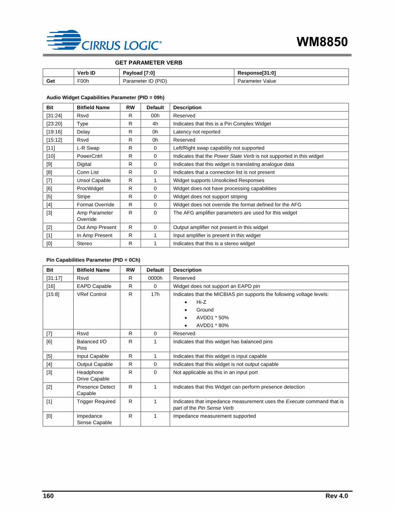
WM8850
160 Rev 4.0
GET PARAMETER VERB
Verb ID Payload [7:0] Response[31:0]
Get F00h Parameter ID (PID) Parameter Value
Audio Widget Capabilities Parameter (PID = 09h)
Bit Bitfield Name RW Default Description
[31:24] Rsvd R 00h Reserved
[23:20] Type R 4h Indicates that this is a Pin Complex Widget
[19:16] Delay R 0h Latency not reported
[15:12] Rsvd R 0h Reserved
[11] L-R Swap R 0 Left/Right swap capability not supported
[10] PowerCntrl R 0 Indicates that the Power State Verb is not supported in this widget
[9] Digital R 0 Indicates that this widget is translating analogue data
[8] Conn List R 0 Indicates that a connection list is not present
[7] Unsol Capable R 1 Widget supports Unsolicited Responses
[6] ProcWidget R 0 Widget does not have processing capabilities
[5] Stripe R 0 Widget does not support striping
[4] Format Override R 0 Widget does not override the format defined for the AFG
[3] Amp Parameter
Override
R 0 The AFG amplifier parameters are used for this widget
[2] Out Amp Present R 0 Output amplifier not present in this widget
[1] In Amp Present R 1 Input amplifier is present in this widget
[0] Stereo R 1 Indicates that this is a stereo widget
Pin Capabilities Parameter (PID = 0Ch)
Bit Bitfield Name RW Default Description
[31:17] Rsvd R 0000h Reserved
[16] EAPD Capable R 0 Widget does not support an EAPD pin
[15:8] VRef Control R 17h Indicates that the MICBIAS pin supports the following voltage levels:
Hi-Z
Ground
AVDD1 * 50%
AVDD1 * 80%
[7] Rsvd R 0 Reserved
[6] Balanced I/O
Pins
R 1 Indicates that this widget has balanced pins
[5] Input Capable R 1 Indicates that this widget is input capable
[4] Output Capable R 0 Indicates that this widget is not output capable
[3] Headphone
Drive Capable
R 0 Not applicable as this in an input port
[2] Presence Detect
Capable
R 1 Indicates that this Widget can perform presence detection
[1] Trigger Required R 1 Indicates that impedance measurement uses the Execute command that is
part of the Pin Sense Verb
[0] Impedance
Sense Capable
R 1 Impedance measurement supported

WM8850
Rev 4.0 161
00h
01h
02h
03h
04h
05h
06h
07h
08h
09h
0Ah
0Bh
0Ch
0Dh
0Eh
0Fh
10h
11h
12h
13h
14h
15h
16h
17h
PIN WIDGET CONTROL VERB
Verb ID Payload [7:0] Response[31:0]
Get F07h 00h Bits [31:0] in the table below
Set 707h Bits [7:0] in the table below 00000000h
Bit Bitfield Name RW Default Description
[31:8] Rsvd R 000000h Reserved
[7] H-Phn Enable R 0 Not applicable as this in an input port
[6] Out Enable R 0 Not applicable as this in an input port
[5] In Enable RW 1 Controls the input path:
0 = Input path is disabled
1 = Input path is enabled
[4:3] Rsvd R 0 Reserved
[2:0] VRefEn RW 0h MICBIAS control:
0h = Hi-Z
1h = AVDD1 * 50%
2h = Ground (0V)
3h = Reserved
4h = AVDD1 * 80%
5h-7h = Reserved
Note: If VRefEn is set to a reserved value, the value programmed will be
0h (Hi-Z) to avoid any potential damage to external components
UNSOLICITED RESPONSE VERB
Verb ID Payload [7:0] Response[31:0]
Get F08h 00h Bits [31:0] in the table below
Set 708h Bits [7:0] in the table below 00000000h
Bit Bitfield Name RW Default Description
[31:8] Rsvd R 000000h Reserved
[7] Enable RW 0 0 = Unsolicited Responses disabled for this node
1 = Unsolicited Responses enabled for this node
[6] Rsvd R 0 Reserved
[5:0] Tag RW 0Dh A software programmable tag value that is returned in the top six bits
(31:26) of every Unsolicited Response from this node.
The default for Tag is equal to the Node ID.
Note: The Unsolicited Response for the AFG node is defined in the “Unsolicited Responses” section.
PIN SENSE VERB
Verb ID Payload [7:0] Response[31:0]
Get F09h 00h Bits [31:0] in the table below
Execute 709h 00h 00000000h
Bit Bitfield Name RW Default Description
[31] Presence Detect R 0 0 = nothing plugged into Port-B
1 = something plugged into Port-B
[30:0] Impedance
Sense
R 7FFFFFFFh Impedance sense value:
7FFFFFFFh = measurement not ready
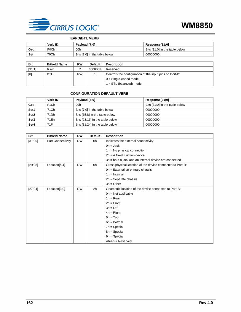
WM8850
162 Rev 4.0
EAPD/BTL VERB
Verb ID Payload [7:0] Response[31:0]
Get F0Ch 00h Bits [31:0] in the table below
Set 70Ch Bits [7:0] in the table below 00000000h
Bit Bitfield Name RW Default Description
[31:1] Rsvd R 000000h Reserved
[0] BTL RW 1 Controls the configuration of the input pins on Port-B:
0 = Single-ended mode
1 = BTL (balanced) mode
CONFIGURATION DEFAULT VERB
Verb ID Payload [7:0] Response[31:0]
Get F1Ch 00h Bits [31:0] in the table below
Set1 71Ch Bits [7:0] in the table below 00000000h
Set2 71Dh Bits [15:8] in the table below 00000000h
Set3 71Eh Bits [23:16] in the table below 00000000h
Set4 71Fh Bits [31:24] in the table below 00000000h
Bit Bitfield Name RW Default Description
[31:30] Port Connectivity RW 0h Indicates the external connectivity:
0h = Jack
1h = No physical connection
2h = A fixed function device
3h = both a jack and an internal device are connected
[29:28] Location[5:4] RW 0h Gross physical location of the device connected to Port-B:
0h = External on primary chassis
1h = Internal
2h = Separate chassis
3h = Other
[27:24] Location[3:0] RW 2h Geometric location of the device connected to Port-B:
0h = Not applicable
1h = Rear
2h = Front
3h = Left
4h = Right
5h = Top
6h = Bottom
7h = Special
8h = Special
9h = Special
Ah-Fh = Reserved

WM8850
Rev 4.0 163
00h
01h
02h
03h
04h
05h
06h
07h
08h
09h
0Ah
0Bh
0Ch
0Dh
0Eh
0Fh
10h
11h
12h
13h
14h
15h
16h
17h
Bit Bitfield Name RW Default Description
[23:20] Default Device RW Ah Indicates the intended use of Port-B:
0h = Line out
1h = Speaker
2h = Headphone out
3h = CD
4h = S/PDIF out
5h = Digital other out
6h = Modem line side
7h = Modem handset side
8h = Line in
9h = AUX
Ah = Mic in
Bh = Telephony
Ch = S/PDIF in
Dh = Digital other in
Eh = Reserved
Fh = Other
[19:16] Connection Type RW 1h Indicates the type of physical interface on Port-B:
0h = Unknown
1h = 3.5mm stereo/mono jack
2h = ¼” stereo/mono jack
3h = ATAPI internal
4h = RCA jack (for analogue audio or coaxial S/PDIF)
5h = Optical
6h = Other digital
7h = Other analogue
8h = Multi-channel analogue (DIN)
9h = XLR/Professional
Ah = RJ-11 (modem)
Bh = Combination
Ch-Eh = Reserved
Fh = Other
[15:12] Colour RW 9h Indicates the colour of the physical jack on Port-B:
0h = Unknown
1h = Black
2h = Grey
3h = Blue
4h = Green
5h = Red
6h = Orange
7h = Yellow
8h = Purple
9h = Pink
Ah-Dh = Reserved
Eh = White
Fh = Other

WM8850
164 Rev 4.0
Bit Bitfield Name RW Default Description
[11:8] Misc RW 0h Presence detection override:
0 = Presence detection indicated by Pin Capabilities Parameter
1 = Presence detection not supported. If the Pin Capabilities Parameter
indicates that that presence detection is supported by the node, then this
bit is used to override it to indicate the external circuitry is not capable of
supporting presence detect
All other values are reserved
[7:4] Default
Association
RW Fh Association number:
0h = Reserved
1h-Eh = Multi Channel or Single Pin Widget
Fh = Single Pin Widget Only
[3:0] Sequence RW 0h Sequence number used to define individual channel pairs within a stream.
All values (0h-Fh) are available for use. Use a value of 0h for Single Pin
Widget.
Note: The Configuration Default Verb is not reset to its default value during a reset from any source. The settings are only lost
when digital power is removed from the WM8850. When digital power is restored, the System BIOS must restore the settings.
UNSOLICITED RESPONSE PRIORITY CONTROL VERB (VENDOR-SPECIFIC)
Verb ID Payload [7:0] Response[31:0]
Get F8Eh 00h Bits [31:0] in the table below
Set 78Eh Bits [7:0] in the table below 00000000h
Bit Bitfield Name RW Default Description
[31:5] Rsvd R 0000000h Reserved
[4:0] Priority RW 00h Assigns a priority setting for queued Unsolicited Responses. Nodes with
the lowest value have the highest priority, and so go to the front of the
Unsolicited Response queue. Nodes with the same value for priority are
queued on first-to-trigger basis.
00h = Highest priority
…
1Fh = Lowest priority
DIFFERENTIAL VERB (VENDOR-SPECIFIC)
Verb ID Payload [7:0] Response[31:0]
Get FA3h 00h Bits [31:0] in the table below
Set 7A3h Bits [7:0] in the table below 00000000h
Bit Bitfield Name RW Default Description
[31:1] Rsvd R 0000000h Reserved
[0] Differential Mode RW 1 Differential mode:
0 = Differential (Microphone)
1 = Pseudo-differential

WM8850
Rev 4.0 165
00h
01h
02h
03h
04h
05h
06h
07h
08h
09h
0Ah
0Bh
0Ch
0Dh
0Eh
0Fh
10h
11h
12h
13h
14h
15h
16h
17h
AUTO-MUTE CONTROL VERB (VENDOR-SPECIFIC)
Verb ID Payload [7:0] Response[31:0]
Get FB0h 00h Bits [31:0] in the table below
Set 7B0h Bits [7:0] in the table below 00000000h
Bit Bitfield Name RW Default Description
[31:1] Rsvd R 0000000h Reserved
[0] PD_AUTOMUTE RW 0 Controls the WM8850 automute behavior when there is nothing plugged
into Port-B:
0 = Automute disabled
1 = Automute enabled
Note: When PD_AUTOMUTE=1 and Presence Detect=1 the WM8850 will
replace the samples in the stream with zeros

WM8850
166 Rev 4.0

WM8850
Rev 4.0 167
00h
01h
02h
03h
04h
05h
06h
07h
08h
09h
0Ah
0Bh
0Ch
0Dh
0Eh
0Fh
10h
11h
12h
13h
14h
15h
16h
17h
PORT-D PIN COMPLEX WIDGET (NID = 0EH)
AMPLIFIER GAIN/MUTE VERB
Verb ID Payload [15:0] Response[31:0]
Get Bh 2000h Bits [31:0] in the response table below –
applies to the left channel only
Get Bh 0000h Bits [31:0] in the response table below –
applies to the right channel only
Set 3h Bits [15:0] in the set table below 00000000h
Response Table:
Bit Bitfield Name RW Default Description
[31:8] Rsvd R 000000h Reserved
[7] Amplifier Mute R 0 Shows the amplifier mute status of the selected channel:
0 = Normal
1 = Muted
[6:0] Amplifier Gain R 18h Shows the amplifier gain setting (step number) for the selected channel.
The actual gain applied is determined by the Input Amplifier Capabilities
Parameter, and is shown below for convenience:
00h = −12dB
01h = −11.5dB
… 0.5dB steps
18h = 0dB
… 0.5dB steps
57h = +31.5dB
58h = +32dB
Set Table:
Bit Bitfield Name RW Default Description
[15] Set Output Amp W 0 Not applicable to this widget
[14] Set Input Amp W 1 Indicates that the programming refers to the input amplifier on this widget
[13] Set Left Amp W 1 0 = Left channel amplifier does not accept the values in Mute or Gain
fields
1 = Left channel amplifier does accept the values in the Mute and Gain
fields
[12] Set Right Amp W 1 0 = Right channel amplifier does not accept the values in Mute or Gain
fields
1 = Right channel amplifier does accept the values in the Mute and Gain
fields
[11:8] Index W 0h Not applicable to this widget
[7] Mute W 0 0 = Normal operation
1 = Mute
Note: When mute is applied to a channel, the data value is overwritten
with all zeros.
[6:0] Gain W 18h Step number of the gain – see Amplifier Gain in response table above for
details of actual gain values
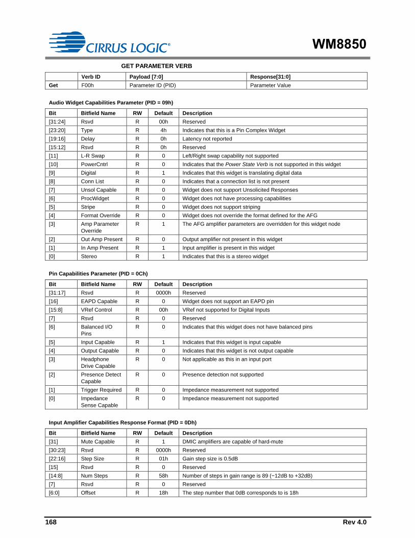
WM8850
168 Rev 4.0
GET PARAMETER VERB
Verb ID Payload [7:0] Response[31:0]
Get F00h Parameter ID (PID) Parameter Value
Audio Widget Capabilities Parameter (PID = 09h)
Bit Bitfield Name RW Default Description
[31:24] Rsvd R 00h Reserved
[23:20] Type R 4h Indicates that this is a Pin Complex Widget
[19:16] Delay R 0h Latency not reported
[15:12] Rsvd R 0h Reserved
[11] L-R Swap R 0 Left/Right swap capability not supported
[10] PowerCntrl R 0 Indicates that the Power State Verb is not supported in this widget
[9] Digital R 1 Indicates that this widget is translating digital data
[8] Conn List R 0 Indicates that a connection list is not present
[7] Unsol Capable R 0 Widget does not support Unsolicited Responses
[6] ProcWidget R 0 Widget does not have processing capabilities
[5] Stripe R 0 Widget does not support striping
[4] Format Override R 0 Widget does not override the format defined for the AFG
[3] Amp Parameter
Override
R 1 The AFG amplifier parameters are overridden for this widget node
[2] Out Amp Present R 0 Output amplifier not present in this widget
[1] In Amp Present R 1 Input amplifier is present in this widget
[0] Stereo R 1 Indicates that this is a stereo widget
Pin Capabilities Parameter (PID = 0Ch)
Bit Bitfield Name RW Default Description
[31:17] Rsvd R 0000h Reserved
[16] EAPD Capable R 0 Widget does not support an EAPD pin
[15:8] VRef Control R 00h VRef not supported for Digital Inputs
[7] Rsvd R 0 Reserved
[6] Balanced I/O
Pins
R 0 Indicates that this widget does not have balanced pins
[5] Input Capable R 1 Indicates that this widget is input capable
[4] Output Capable R 0 Indicates that this widget is not output capable
[3] Headphone
Drive Capable
R 0 Not applicable as this in an input port
[2] Presence Detect
Capable
R 0 Presence detection not supported
[1] Trigger Required R 0 Impedance measurement not supported
[0] Impedance
Sense Capable
R 0 Impedance measurement not supported
Input Amplifier Capabilities Response Format (PID = 0Dh)
Bit Bitfield Name RW Default Description
[31] Mute Capable R 1 DMIC amplifiers are capable of hard-mute
[30:23] Rsvd R 0000h Reserved
[22:16] Step Size R 01h Gain step size is 0.5dB
[15] Rsvd R 0 Reserved
[14:8] Num Steps R 58h Number of steps in gain range is 89 (−12dB to +32dB)
[7] Rsvd R 0 Reserved
[6:0] Offset R 18h The step number that 0dB corresponds to is 18h

WM8850
Rev 4.0 169
00h
01h
02h
03h
04h
05h
06h
07h
08h
09h
0Ah
0Bh
0Ch
0Dh
0Eh
0Fh
10h
11h
12h
13h
14h
15h
16h
17h
PIN WIDGET CONTROL VERB
Verb ID Payload [7:0] Response[31:0]
Get F07h 00h Bits [31:0] in the table below
Set 707h Bits [7:0] in the table below 00000000h
Bit Bitfield Name RW Default Description
[31:8] Rsvd R 000000h Reserved
[7] H-Phn Enable R 0 Not applicable as this in an input port
[6] Out Enable R 0 Not applicable as this in an input port
[5] In Enable RW 1 Controls the input path:
0 = Input path is disabled
1 = Input path is enabled
[4:3] Rsvd R 0h Reserved
[2:0] VRefEn R 0h Selectable VRef not supported
CONFIGURATION DEFAULT VERB
Verb ID Payload [7:0] Response[31:0]
Get F1Ch 00h Bits [31:0] in the table below
Set1 71Ch Bits [7:0] in the table below 00000000h
Set2 71Dh Bits [15:8] in the table below 00000000h
Set3 71Eh Bits [23:16] in the table below 00000000h
Set4 71Fh Bits [31:24] in the table below 00000000h
Bit Bitfield Name RW Default Description
[31:30] Port Connectivity RW 0h Indicates the external connectivity:
0h = Jack
1h = No physical connection
2h = A fixed function device
3h = both a jack and an internal device are connected
[29:28] Location[5:4] RW 1h Gross physical location of the device connected to Port-D:
0h = External on primary chassis
1h = Internal
2h = Separate chassis
3h = Other
[27:24] Location[3:0] RW 0h Geometric location of the device connected to Port-D:
0h = Not applicable
1h = Rear
2h = Front
3h = Left
4h = Right
5h = Top
6h = Bottom
7h = Special
8h = Special
9h = Special
Ah-Fh = Reserved
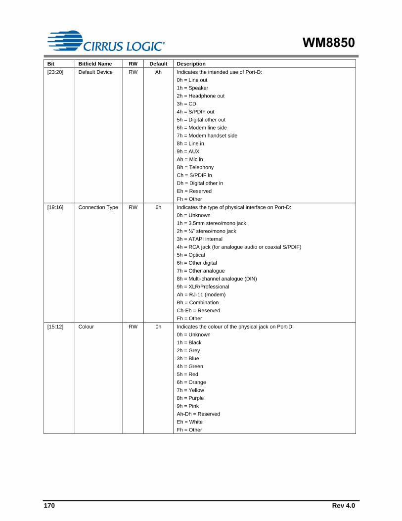
WM8850
170 Rev 4.0
Bit Bitfield Name RW Default Description
[23:20] Default Device RW Ah Indicates the intended use of Port-D:
0h = Line out
1h = Speaker
2h = Headphone out
3h = CD
4h = S/PDIF out
5h = Digital other out
6h = Modem line side
7h = Modem handset side
8h = Line in
9h = AUX
Ah = Mic in
Bh = Telephony
Ch = S/PDIF in
Dh = Digital other in
Eh = Reserved
Fh = Other
[19:16] Connection Type RW 6h Indicates the type of physical interface on Port-D:
0h = Unknown
1h = 3.5mm stereo/mono jack
2h = ¼” stereo/mono jack
3h = ATAPI internal
4h = RCA jack (for analogue audio or coaxial S/PDIF)
5h = Optical
6h = Other digital
7h = Other analogue
8h = Multi-channel analogue (DIN)
9h = XLR/Professional
Ah = RJ-11 (modem)
Bh = Combination
Ch-Eh = Reserved
Fh = Other
[15:12] Colour RW 0h Indicates the colour of the physical jack on Port-D:
0h = Unknown
1h = Black
2h = Grey
3h = Blue
4h = Green
5h = Red
6h = Orange
7h = Yellow
8h = Purple
9h = Pink
Ah-Dh = Reserved
Eh = White
Fh = Other

WM8850
Rev 4.0 171
00h
01h
02h
03h
04h
05h
06h
07h
08h
09h
0Ah
0Bh
0Ch
0Dh
0Eh
0Fh
10h
11h
12h
13h
14h
15h
16h
17h
Bit Bitfield Name RW Default Description
[11:8] Misc RW 0h Presence detection override:
0h = Presence detection indicated by Pin Capabilities Parameter
1h = Presence detection not supported. If the Pin Capabilities Parameter
indicates that that presence detection is supported by the node, then this
bit is used to override it to indicate the external circuitry is not capable of
supporting presence detect
All other values are reserved
[7:4] Default
Association
RW Fh Association number:
0h = Reserved
1h-Eh = Multi Channel or Single Pin Widget
Fh = Single Pin Widget Only
[3:0] Sequence RW 0h Sequence number used to define individual channel pairs within a stream.
All values (0h-Fh) are available for use. Use a value of 0 for Single Pin
Widget.
Note: The Configuration Default Verb is not reset to its default value during a reset from any source. The settings are only lost
when digital power is removed from the WM8850. When digital power is restored, the System BIOS must restore the settings.

WM8850
172 Rev 4.0
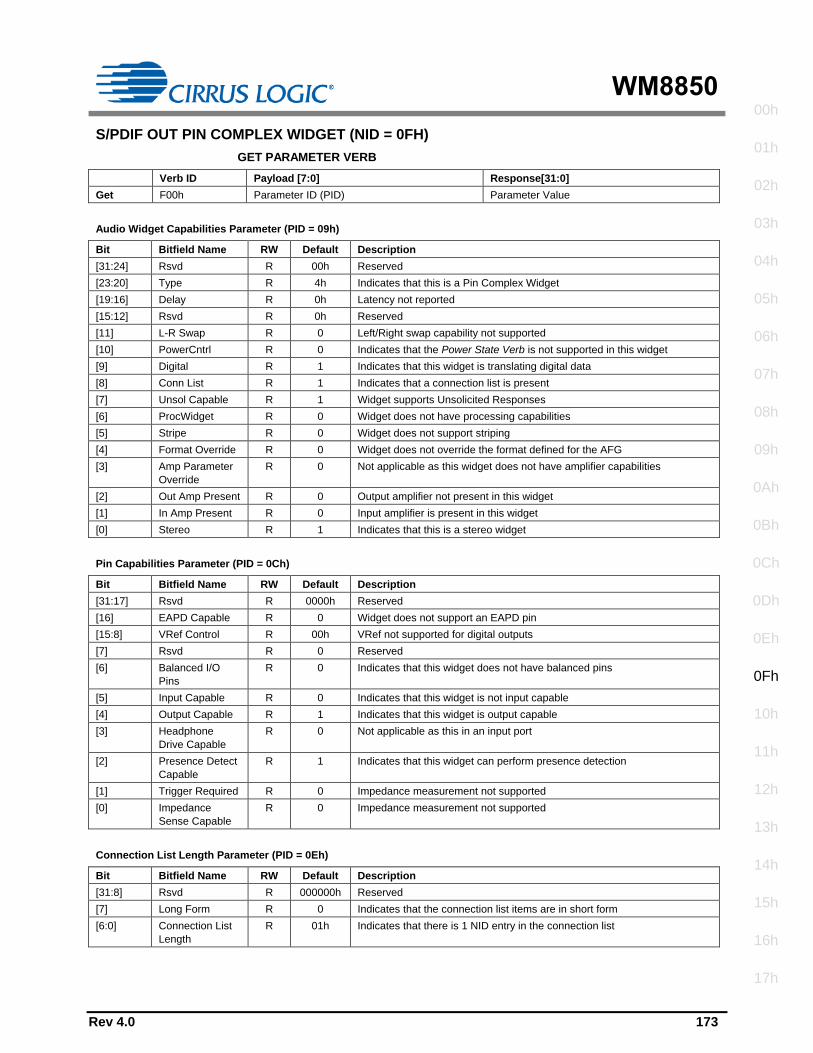
WM8850
Rev 4.0 173
00h
01h
02h
03h
04h
05h
06h
07h
08h
09h
0Ah
0Bh
0Ch
0Dh
0Eh
0Fh
10h
11h
12h
13h
14h
15h
16h
17h
S/PDIF OUT PIN COMPLEX WIDGET (NID = 0FH)
GET PARAMETER VERB
Verb ID Payload [7:0] Response[31:0]
Get F00h Parameter ID (PID) Parameter Value
Audio Widget Capabilities Parameter (PID = 09h)
Bit Bitfield Name RW Default Description
[31:24] Rsvd R 00h Reserved
[23:20] Type R 4h Indicates that this is a Pin Complex Widget
[19:16] Delay R 0h Latency not reported
[15:12] Rsvd R 0h Reserved
[11] L-R Swap R 0 Left/Right swap capability not supported
[10] PowerCntrl R 0 Indicates that the Power State Verb is not supported in this widget
[9] Digital R 1 Indicates that this widget is translating digital data
[8] Conn List R 1 Indicates that a connection list is present
[7] Unsol Capable R 1 Widget supports Unsolicited Responses
[6] ProcWidget R 0 Widget does not have processing capabilities
[5] Stripe R 0 Widget does not support striping
[4] Format Override R 0 Widget does not override the format defined for the AFG
[3] Amp Parameter
Override
R 0 Not applicable as this widget does not have amplifier capabilities
[2] Out Amp Present R 0 Output amplifier not present in this widget
[1] In Amp Present R 0 Input amplifier is present in this widget
[0] Stereo R 1 Indicates that this is a stereo widget
Pin Capabilities Parameter (PID = 0Ch)
Bit Bitfield Name RW Default Description
[31:17] Rsvd R 0000h Reserved
[16] EAPD Capable R 0 Widget does not support an EAPD pin
[15:8] VRef Control R 00h VRef not supported for digital outputs
[7] Rsvd R 0 Reserved
[6] Balanced I/O
Pins
R 0 Indicates that this widget does not have balanced pins
[5] Input Capable R 0 Indicates that this widget is not input capable
[4] Output Capable R 1 Indicates that this widget is output capable
[3] Headphone
Drive Capable
R 0 Not applicable as this in an input port
[2] Presence Detect
Capable
R 1 Indicates that this widget can perform presence detection
[1] Trigger Required R 0 Impedance measurement not supported
[0] Impedance
Sense Capable
R 0 Impedance measurement not supported
Connection List Length Parameter (PID = 0Eh)
Bit Bitfield Name RW Default Description
[31:8] Rsvd R 000000h Reserved
[7] Long Form R 0 Indicates that the connection list items are in short form
[6:0] Connection List
Length
R 01h Indicates that there is 1 NID entry in the connection list

WM8850
174 Rev 4.0
GET CONNECTION LIST ENTRY VERB
Verb ID Payload [7:0] Response[31:0]
Get F02h 00h Bits [31:0] in the table below
Bit Bitfield Name RW Default Description
[31:24] Conn List Entry 3 R 00h Unused connection list entry
[23:16] Conn List Entry 2 R 00h Unused connection list entry
[15:8] Conn List Entry 1 R 00h Unused connection list entry
[7:0] Conn List Entry 0 R 04h Indicates that the S/PDIF Out Pin Widget connects to the S/PDIF Tx 1
Widget (NID = 04h)
PIN WIDGET CONTROL VERB
Verb ID Payload [7:0] Response[31:0]
Get F07h 00h Bits [31:0] in the table below
Set 707h Bits [7:0] in the table below 00000000h
Bit Bitfield Name RW Default Description
[31:8] Rsvd R 000000h Reserved
[7] H-Phn Enable R 0 Not applicable for S/PDIF Out
[6] Out Enable RW 1 Controls the output path:
0 = Output path is disabled
1 = Output path is enabled
Note: If S/PDIF Out sources the S/PDIF Tx 1 Widget and OutEnable=0,
the S/PDIF signal is still transmitted, but the payload of the S/PDIF signal
is filled with zeros. In this way, the OutEnable register acts as a S/PDIF
Mute. When sourcing the S/PDIF TX 1 Widget, the user can have the
S/PDIF Out pin drive 0 by setting DigEn (in the S/PDIF TX 1 Widget) to 0.
Note: If S/PDIF Out sources the S/PDIF In widget and OutEnable=0, the
S/PDIF Out pin drives zero. The Digen register has no context in this
configuration, and is ignored.
[5] In Enable R 0 Not applicable for S/PDIF Out
[4:3] Rsvd R 0h Reserved
[2:0] VRefEn RW 0h Selectable VRef not supported
UNSOLICITED RESPONSE VERB
Verb ID Payload [7:0] Response[31:0]
Get F08h 00h Bits [31:0] in the table below
Set 708h Bits [7:0] in the table below 00000000h
Bit Bitfield Name RW Default Description
[31:8] Rsvd R 000000h Reserved
[7] Enable RW 0 0 = Unsolicited Responses disabled for this node
1 = Unsolicited Responses enabled for this node
[6] Rsvd R 0 Reserved
[5:0] Tag RW 0Fh A software programmable tag value that is returned in the top six bits
(31:26) of every Unsolicited Response from this node.
The default for Tag is equal to the Node ID.
Note: The Unsolicited Response for the AFG node is defined in the “Unsolicited Responses” section.

WM8850
Rev 4.0 175
00h
01h
02h
03h
04h
05h
06h
07h
08h
09h
0Ah
0Bh
0Ch
0Dh
0Eh
0Fh
10h
11h
12h
13h
14h
15h
16h
17h
PIN SENSE VERB
Verb ID Payload [7:0] Response[31:0]
Get F09h 00h Bits [31:0] in the table below
Bit Bitfield Name RW Default Description
[31] Presence Detect R 0 0 = nothing plugged into S/PDIF Out
1 = something plugged into S/PDIF Out
[30:0] Impedance
Sense
R 00000000h Impedance sense not supported
CONFIGURATION DEFAULT VERB
Verb ID Payload [7:0] Response[31:0]
Get F1Ch 00h Bits [31:0] in the table below
Set1 71Ch Bits [7:0] in the table below 00000000h
Set2 71Dh Bits [15:8] in the table below 00000000h
Set3 71Eh Bits [23:16] in the table below 00000000h
Set4 71Fh Bits [31:24] in the table below 00000000h
Bit Bitfield Name RW Default Description
[31:30] Port Connectivity RW 0h Indicates the external connectivity:
0h = Jack
1h = No physical connection
2h = A fixed function device
3h = both a jack and an internal device are connected
[29:28] Location[5:4] RW 0h Gross physical location of the device connected to S/PDIF Out:
0h = External on primary chassis
1h = Internal
2h = Separate chassis
3h = Other
[27:24] Location[3:0] RW 1h Geometric location of the device connected to S/PDIF Out:
0h = Not applicable
1h = Rear
2h = Front
3h = Left
4h = Right
5h = Top
6h = Bottom
7h = Special
8h = Special
9h = Special
Ah-Fh = Reserved
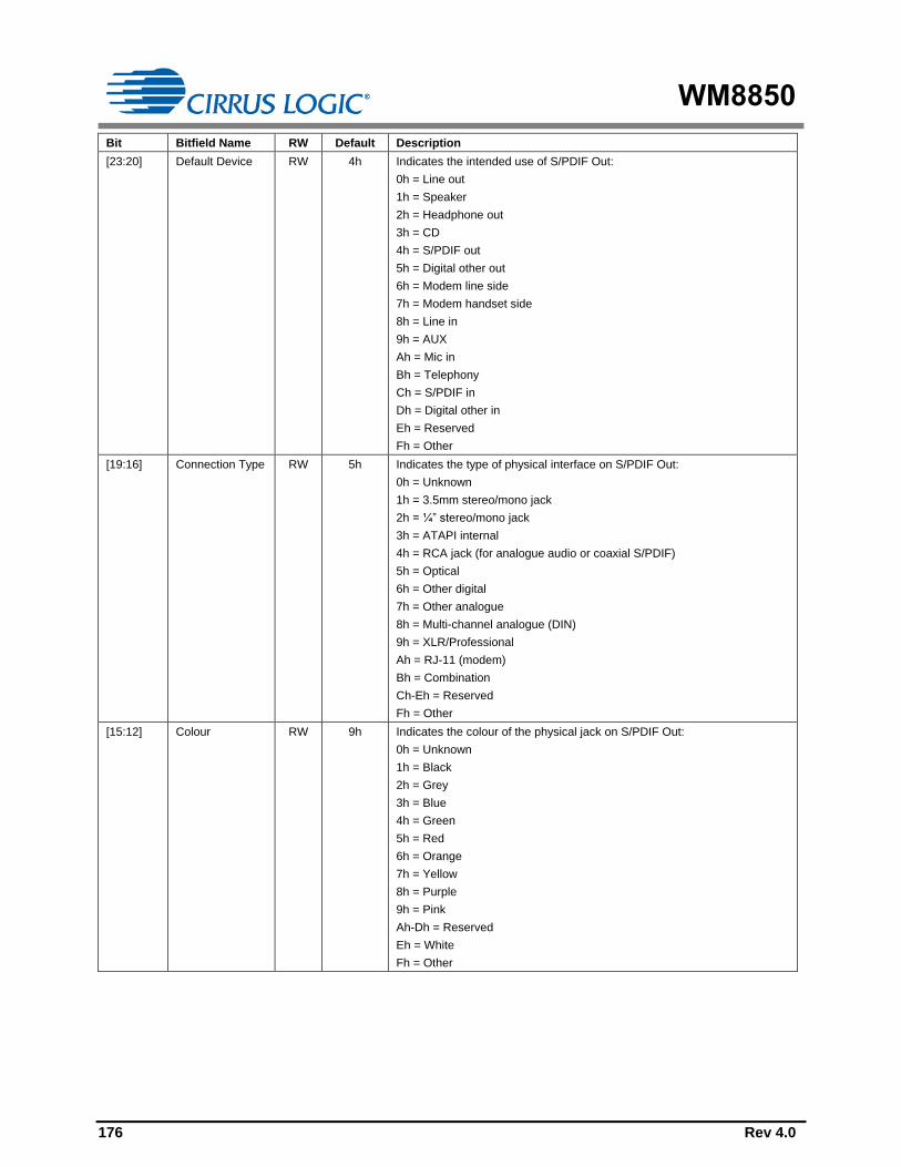
WM8850
176 Rev 4.0
Bit Bitfield Name RW Default Description
[23:20] Default Device RW 4h Indicates the intended use of S/PDIF Out:
0h = Line out
1h = Speaker
2h = Headphone out
3h = CD
4h = S/PDIF out
5h = Digital other out
6h = Modem line side
7h = Modem handset side
8h = Line in
9h = AUX
Ah = Mic in
Bh = Telephony
Ch = S/PDIF in
Dh = Digital other in
Eh = Reserved
Fh = Other
[19:16] Connection Type RW 5h Indicates the type of physical interface on S/PDIF Out:
0h = Unknown
1h = 3.5mm stereo/mono jack
2h = ¼” stereo/mono jack
3h = ATAPI internal
4h = RCA jack (for analogue audio or coaxial S/PDIF)
5h = Optical
6h = Other digital
7h = Other analogue
8h = Multi-channel analogue (DIN)
9h = XLR/Professional
Ah = RJ-11 (modem)
Bh = Combination
Ch-Eh = Reserved
Fh = Other
[15:12] Colour RW 9h Indicates the colour of the physical jack on S/PDIF Out:
0h = Unknown
1h = Black
2h = Grey
3h = Blue
4h = Green
5h = Red
6h = Orange
7h = Yellow
8h = Purple
9h = Pink
Ah-Dh = Reserved
Eh = White
Fh = Other

WM8850
Rev 4.0 177
00h
01h
02h
03h
04h
05h
06h
07h
08h
09h
0Ah
0Bh
0Ch
0Dh
0Eh
0Fh
10h
11h
12h
13h
14h
15h
16h
17h
Bit Bitfield Name RW Default Description
[11:8] Misc RW 1h Presence detection override:
0 = Presence detection indicated by Pin Capabilities Parameter
1 = Presence detection not supported. If the Pin Capabilities Parameter
indicates that that presence detection is supported by the node, then this
bit is used to override it to indicate the external circuitry is not capable of
supporting presence detect
All other values are reserved
[7:4] Default
Association
RW Fh Association number:
0h = Reserved
1h-Eh = Multi Channel or Single Pin Widget
Fh = Single Pin Widget Only
[3:0] Sequence RW 0h Sequence number used to define individual channel pairs within a stream.
All values (0h-Fh) are available for use. Use a value of 0 for Single Pin
Widget.
Note: The Configuration Default Verb is not reset to its default value during a reset from any source. The settings are only lost
when digital power is removed from the WM8850. When digital power is restored, the System BIOS must restore the settings.
INTERNAL PATH VERB (VENDOR-SPECIFIC)
Verb ID Payload [7:0] Response[31:0]
Get F73h 00h Bits [31:0] in the table below
Set 773h Bits [7:0] in the table below 00000000h
Bit Bitfield Name RW Default Description
[31:1] Rsvd R 0000000h Reserved
[7:0] Path Sel RW 4h Selects source of S/PDIF Out node:
04h = S/PDIF Tx 1
10h = S/PDIF In
Note: This verb can overwrite the path setup by the connection list
UNSOLICITED RESPONSE PRIORITY CONTROL VERB (VENDOR-SPECIFIC)
Verb ID Payload [7:0] Response[31:0]
Get F8Eh 00h Bits [31:0] in the table below
Set 78Eh Bits [7:0] in the table below 00000000h
Bit Bitfield Name RW Default Description
[31:5] Rsvd R 0000000h Reserved
[4:0] Priority RW 00h Assigns a priority setting for queued Unsolicited Responses. Nodes with
the lowest value have the highest priority, and so go to the front of the
Unsolicited Response queue. Nodes with the same value for priority are
queued on first-to-trigger basis.
00h = Highest priority
…
1Fh = Lowest priority

WM8850
178 Rev 4.0
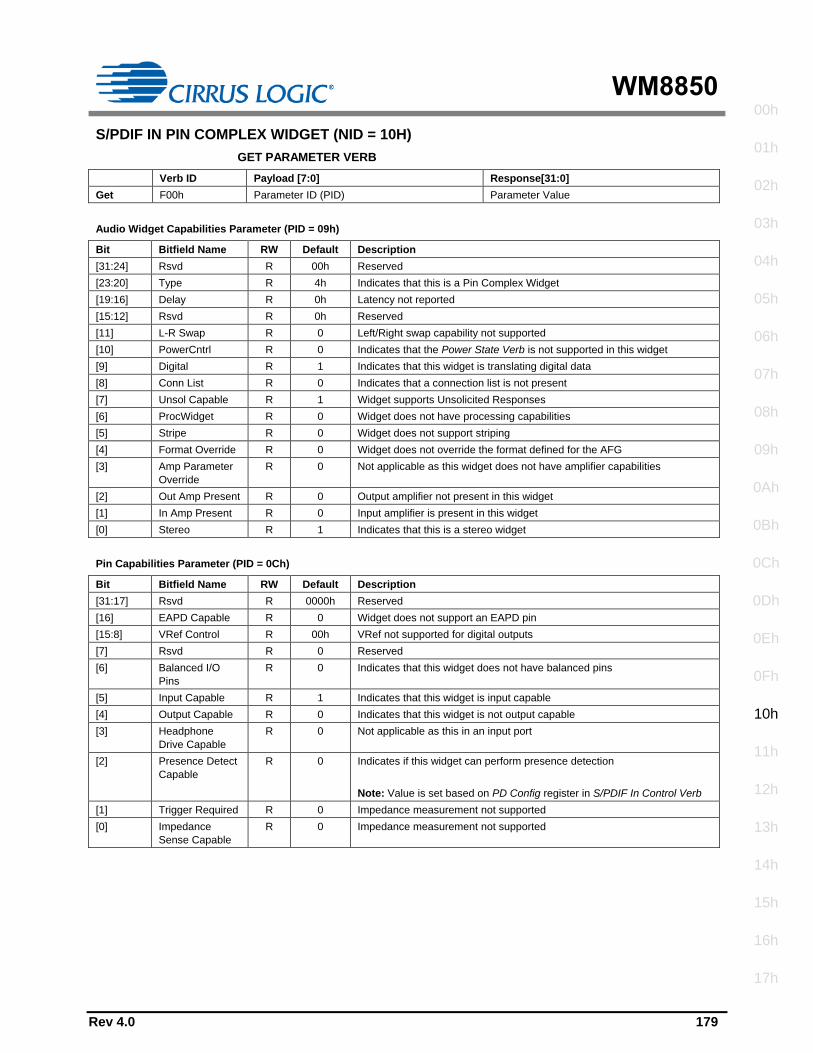
WM8850
Rev 4.0 179
00h
01h
02h
03h
04h
05h
06h
07h
08h
09h
0Ah
0Bh
0Ch
0Dh
0Eh
0Fh
10h
11h
12h
13h
14h
15h
16h
17h
S/PDIF IN PIN COMPLEX WIDGET (NID = 10H)
GET PARAMETER VERB
Verb ID Payload [7:0] Response[31:0]
Get F00h Parameter ID (PID) Parameter Value
Audio Widget Capabilities Parameter (PID = 09h)
Bit Bitfield Name RW Default Description
[31:24] Rsvd R 00h Reserved
[23:20] Type R 4h Indicates that this is a Pin Complex Widget
[19:16] Delay R 0h Latency not reported
[15:12] Rsvd R 0h Reserved
[11] L-R Swap R 0 Left/Right swap capability not supported
[10] PowerCntrl R 0 Indicates that the Power State Verb is not supported in this widget
[9] Digital R 1 Indicates that this widget is translating digital data
[8] Conn List R 0 Indicates that a connection list is not present
[7] Unsol Capable R 1 Widget supports Unsolicited Responses
[6] ProcWidget R 0 Widget does not have processing capabilities
[5] Stripe R 0 Widget does not support striping
[4] Format Override R 0 Widget does not override the format defined for the AFG
[3] Amp Parameter
Override
R 0 Not applicable as this widget does not have amplifier capabilities
[2] Out Amp Present R 0 Output amplifier not present in this widget
[1] In Amp Present R 0 Input amplifier is present in this widget
[0] Stereo R 1 Indicates that this is a stereo widget
Pin Capabilities Parameter (PID = 0Ch)
Bit Bitfield Name RW Default Description
[31:17] Rsvd R 0000h Reserved
[16] EAPD Capable R 0 Widget does not support an EAPD pin
[15:8] VRef Control R 00h VRef not supported for digital outputs
[7] Rsvd R 0 Reserved
[6] Balanced I/O
Pins
R 0 Indicates that this widget does not have balanced pins
[5] Input Capable R 1 Indicates that this widget is input capable
[4] Output Capable R 0 Indicates that this widget is not output capable
[3] Headphone
Drive Capable
R 0 Not applicable as this in an input port
[2] Presence Detect
Capable
R 0 Indicates if this widget can perform presence detection
Note: Value is set based on PD Config register in S/PDIF In Control Verb
[1] Trigger Required R 0 Impedance measurement not supported
[0] Impedance
Sense Capable
R 0 Impedance measurement not supported
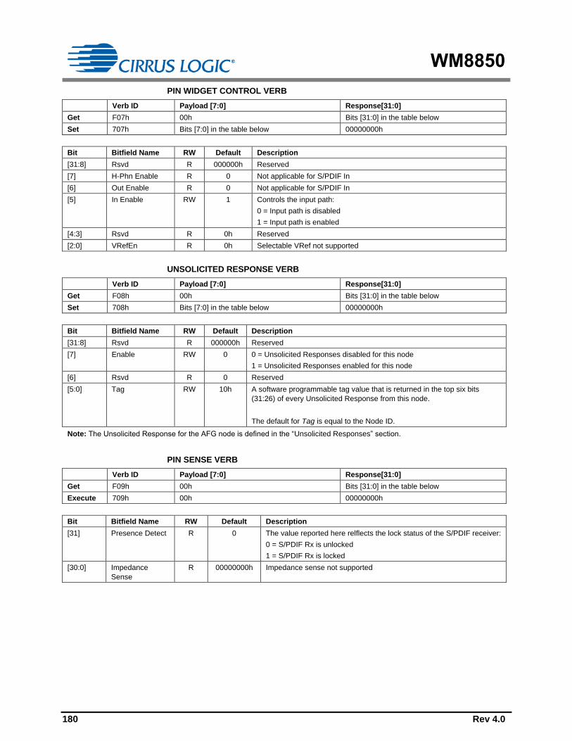
WM8850
180 Rev 4.0
PIN WIDGET CONTROL VERB
Verb ID Payload [7:0] Response[31:0]
Get F07h 00h Bits [31:0] in the table below
Set 707h Bits [7:0] in the table below 00000000h
Bit Bitfield Name RW Default Description
[31:8] Rsvd R 000000h Reserved
[7] H-Phn Enable R 0 Not applicable for S/PDIF In
[6] Out Enable R 0 Not applicable for S/PDIF In
[5] In Enable RW 1 Controls the input path:
0 = Input path is disabled
1 = Input path is enabled
[4:3] Rsvd R 0h Reserved
[2:0] VRefEn R 0h Selectable VRef not supported
UNSOLICITED RESPONSE VERB
Verb ID Payload [7:0] Response[31:0]
Get F08h 00h Bits [31:0] in the table below
Set 708h Bits [7:0] in the table below 00000000h
Bit Bitfield Name RW Default Description
[31:8] Rsvd R 000000h Reserved
[7] Enable RW 0 0 = Unsolicited Responses disabled for this node
1 = Unsolicited Responses enabled for this node
[6] Rsvd R 0 Reserved
[5:0] Tag RW 10h A software programmable tag value that is returned in the top six bits
(31:26) of every Unsolicited Response from this node.
The default for Tag is equal to the Node ID.
Note: The Unsolicited Response for the AFG node is defined in the “Unsolicited Responses” section.
PIN SENSE VERB
Verb ID Payload [7:0] Response[31:0]
Get F09h 00h Bits [31:0] in the table below
Execute 709h 00h 00000000h
Bit Bitfield Name RW Default Description
[31] Presence Detect R 0 The value reported here relflects the lock status of the S/PDIF receiver:
0 = S/PDIF Rx is unlocked
1 = S/PDIF Rx is locked
[30:0] Impedance
Sense
R 00000000h Impedance sense not supported

WM8850
Rev 4.0 181
00h
01h
02h
03h
04h
05h
06h
07h
08h
09h
0Ah
0Bh
0Ch
0Dh
0Eh
0Fh
10h
11h
12h
13h
14h
15h
16h
17h
CONFIGURATION DEFAULT VERB
Verb ID Payload [7:0] Response[31:0]
Get F1Ch 00h Bits [31:0] in the table below
Set1 71Ch Bits [7:0] in the table below 00000000h
Set2 71Dh Bits [15:8] in the table below 00000000h
Set3 71Eh Bits [23:16] in the table below 00000000h
Set4 71Fh Bits [31:24] in the table below 00000000h
Bit Bitfield Name RW Default Description
[31:30] Port Connectivity RW 0h Indicates the external connectivity:
0h = Jack
1h = No physical connection
2h = A fixed function device
3h = both a jack and an internal device are connected
[29:28] Location[5:4] RW 0h Gross physical location of the device connected to SPDIF_IN:
0h = External on primary chassis
1h = Internal
2h = Separate chassis
3h = Other
[27:24] Location[3:0] RW 1h Geometric location of the device connected to SPDIF_IN:
0h = Not applicable
1h = Rear
2h = Front
3h = Left
4h = Right
5h = Top
6h = Bottom
7h = Special
8h = Special
9h = Special
Ah-Fh = Reserved
[23:20] Default Device RW Ch Indicates the intended use of SPDIF_IN:
0h = Line out
1h = Speaker
2h = Headphone out
3h = CD
4h = S/PDIF out
5h = Digital other out
6h = Modem line side
7h = Modem handset side
8h = Line in
9h = AUX
Ah = Mic in
Bh = Telephony
Ch = S/PDIF in
Dh = Digital other in
Eh = Reserved
Fh = Other

WM8850
182 Rev 4.0
Bit Bitfield Name RW Default Description
[19:16] Connection Type RW 5h Indicates the type of physical interface on SPDIF_IN:
0h = Unknown
1h = 3.5mm stereo/mono jack
2h = ¼” stereo/mono jack
3h = ATAPI internal
4h = RCA jack (for analogue audio or coaxial S/PDIF)
5h = Optical
6h = Other digital
7h = Other analogue
8h = Multi-channel analogue (DIN)
9h = XLR/Professional
Ah = RJ-11 (modem)
Bh = Combination
Ch-Eh = Reserved
Fh = Other
[15:12] Colour RW 2h Indicates the colour of the physical jack on SPDIF_IN:
0h = Unknown
1h = Black
2h = Grey
3h = Blue
4h = Green
5h = Red
6h = Orange
7h = Yellow
8h = Purple
9h = Pink
Ah-Dh = Reserved
Eh = White
Fh = Other
[11:8] Misc RW 0h Presence detection override:
0 = Presence detection indicated by Pin Capabilities Parameter
1 = Presence detection not supported. If the Pin Capabilities Parameter
indicates that that presence detection is supported by the node, then this
bit is used to override it to indicate the external circuitry is not capable of
supporting presence detect
All other values are reserved
[7:4] Default
Association
RW Fh Association number:
0h = Reserved
1h-Eh = Multi Channel or Single Pin Widget
Fh = Single Pin Widget Only
[3:0] Sequence RW 0h Sequence number used to define individual channel pairs within a stream.
All values (0h-Fh) are available for use. Use a value of 0h for Single Pin
Widget.
Note: The Configuration Default Verb is not reset to its default value during a reset from any source. The settings are only lost
when digital power is removed from the WM8850. When digital power is restored, the System BIOS must restore the settings.

WM8850
Rev 4.0 183
00h
01h
02h
03h
04h
05h
06h
07h
08h
09h
0Ah
0Bh
0Ch
0Dh
0Eh
0Fh
10h
11h
12h
13h
14h
15h
16h
17h
UNSOLICITED RESPONSE PRIORITY CONTROL VERB (VENDOR-SPECIFIC)
Verb ID Payload [7:0] Response[31:0]
Get F8Eh 00h Bits [31:0] in the table below
Set 78Eh Bits [7:0] in the table below 00000000h
Bit Bitfield Name RW Default Description
[31:5] Rsvd R 0000000h Reserved
[4:0] Priority RW 00h Assigns a priority setting for queued Unsolicited Responses. Nodes with
the lowest value have the highest priority, and so go to the front of the
Unsolicited Response queue. Nodes with the same value for priority are
queued on first-to-trigger basis.
00h = Highest priority
…
1Fh = Lowest priority
GET S/PDIF IN STATUS VERB (VENDOR-SPECIFIC)
Verb ID Payload [7:0] Response[31:0]
Get FA0h 00h Bits [31:0] in the table below
Bit Bitfield Name RW Default Description
[31:4] Rsvd R 0000000h Reserved
[3:1] RATE R 7h Recovered sample rate:
0h = Reserved
1h = Reserved
2h = 96 kHz
3h = 88.2 kHz
4h = 48 kHz
5h = 44.1 kHz
6h = 32 kHz
7h = Sample rate not detected
[0] LOCK R 0 S/PDIF Rx lock flag:
0 = Unlocked
1 = Locked
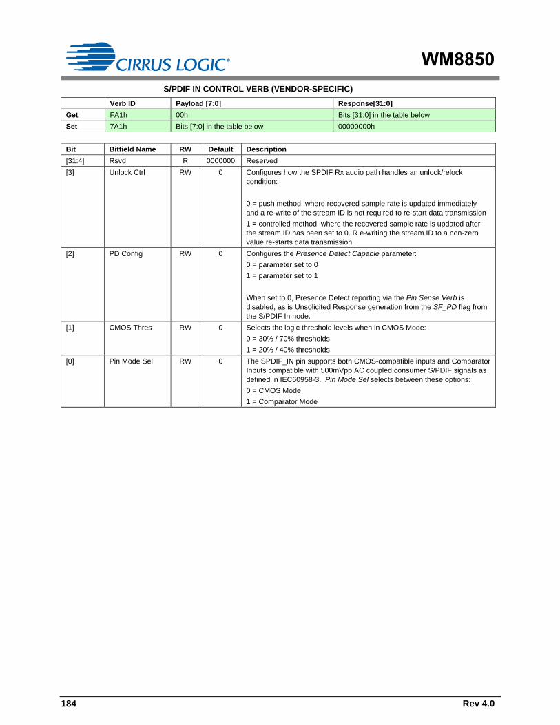
WM8850
184 Rev 4.0
S/PDIF IN CONTROL VERB (VENDOR-SPECIFIC)
Verb ID Payload [7:0] Response[31:0]
Get FA1h 00h Bits [31:0] in the table below
Set 7A1h Bits [7:0] in the table below 00000000h
Bit Bitfield Name RW Default Description
[31:4] Rsvd R 0000000 Reserved
[3] Unlock Ctrl RW 0 Configures how the SPDIF Rx audio path handles an unlock/relock
condition:
0 = push method, where recovered sample rate is updated immediately
and a re-write of the stream ID is not required to re-start data transmission
1 = controlled method, where the recovered sample rate is updated after
the stream ID has been set to 0. R e-writing the stream ID to a non-zero
value re-starts data transmission.
[2] PD Config RW 0 Configures the Presence Detect Capable parameter:
0 = parameter set to 0
1 = parameter set to 1
When set to 0, Presence Detect reporting via the Pin Sense Verb is
disabled, as is Unsolicited Response generation from the SF_PD flag from
the S/PDIF In node.
[1] CMOS Thres RW 0 Selects the logic threshold levels when in CMOS Mode:
0 = 30% / 70% thresholds
1 = 20% / 40% thresholds
[0] Pin Mode Sel RW 0 The SPDIF_IN pin supports both CMOS-compatible inputs and Comparator
Inputs compatible with 500mVpp AC coupled consumer S/PDIF signals as
defined in IEC60958-3. Pin Mode Sel selects between these options:
0 = CMOS Mode
1 = Comparator Mode

WM8850
Rev 4.0 185
00h
01h
02h
03h
04h
05h
06h
07h
08h
09h
0Ah
0Bh
0Ch
0Dh
0Eh
0Fh
10h
11h
12h
13h
14h
15h
16h
17h
PORT-A PIN COMPLEX WIDGET (NID = 11H)
GET PARAMETER VERB
Verb ID Payload [7:0] Response[31:0]
Get F00h Parameter ID (PID) Parameter Value
Audio Widget Capabilities Parameter (PID = 09h)
Bit Bitfield Name RW Default Description
[31:24] Rsvd R 00h Reserved
[23:20] Type R 4h Indicates that this is a Pin Complex Widget
[19:16] Delay R 0h Latency not reported
[15:12] Rsvd R 0h Reserved
[11] L-R Swap R 0 Left/Right swap capability not supported
[10] PowerCntrl R 0 Indicates that the Power State Verb is not supported in this widget
[9] Digital R 0 Indicates that this widget is translating analogue data
[8] Conn List R 1 Indicates that a connection list is present
[7] Unsol Capable R 1 Widget supports Unsolicited Responses
[6] ProcWidget R 0 Widget does not have processing capabilities
[5] Stripe R 0 Widget does not support striping
[4] Format Override R 0 Widget does not override the format defined for the AFG
[3] Amp Parameter
Override
R 0 Not applicable as this widget does not have amplifier capabilities
[2] Out Amp Present R 0 Output amplifier not present in this widget
[1] In Amp Present R 0 Input amplifier not present in this widget
[0] Stereo R 1 Indicates that this is a stereo widget
Pin Capabilities Parameter (PID = 0Ch)
Bit Bitfield Name RW Default Description
[31:17] Rsvd R 0000h Reserved
[16] EAPD Capable R 0 Widget does not support an EAPD pin
[15:8] VRef Control R 00h VRef not supported for digital outputs
[7] Rsvd R 0 Reserved
[6] Balanced I/O
Pins
R 0 Indicates that this widget does not have balanced pins
[5] Input Capable R 0 Indicates that this widget is not input capable
[4] Output Capable R 1 Indicates that this widget is output capable
[3] Headphone
Drive Capable
R 1 Indicates that this widget has a headphone driver
[2] Presence Detect
Capable
R 1 Indicates that this widget can perform presence detection
[1] Trigger Required R 0 Impedance measurement not supported
[0] Impedance
Sense Capable
R 0 Impedance measurement not supported
Connection List Length Parameter (PID = 0Eh)
Bit Bitfield Name RW Default Description
[31:8] Rsvd R 000000h Reserved
[7] Long Form R 0 Indicates that the connection list items are in short form
[6:0] Connection List
Length
R 01h Indicates that there is 1 NID entry in the connection list

WM8850
186 Rev 4.0
GET CONNECTION LIST ENTRY VERB
Verb ID Payload [7:0] Response[31:0]
Get F02h 00h Bits [31:0] in the table below
Bit Bitfield Name RW Default Description
[31:24] Conn List Entry 3 R 00h Unused connection list entry
[23:16] Conn List Entry 2 R 00h Unused connection list entry
[15:8] Conn List Entry 1 R 00h Unused connection list entry
[7:0] Conn List Entry 0 R 06h Indicates that the Port-A Pin Widget connects to the DAC1 Widget (NID =
06h)
PIN WIDGET CONTROL VERB
Verb ID Payload [7:0] Response[31:0]
Get F07h 00h Bits [31:0] in the table below
Set 707h Bits [7:0] in the table below 00000000h
Bit Bitfield Name RW Default Description
[31:8] Rsvd R 000000h Reserved
[7] H-Phn Enable RW 0h Headphone amplifier enable:
0 = Disable
1 = Enable
Note: If the H-Phn Enable register is set to 1, the actual gain setting
applied has an offset of −8dB from the setting configured by the Gain
register in the DAC1 Amplifier Gain/Mute Verb.
[6] Out Enable RW 1 Controls the output path:
0 = Output path is disabled
1 = Output path is enabled
[5] In Enable R 0 Not applicable for Port-A
[4:3] Rsvd R 0h Reserved
[2:0] VRefEn R 0h Selectable VRef not supported
UNSOLICITED RESPONSE VERB
Verb ID Payload [7:0] Response[31:0]
Get F08h 00h Bits [31:0] in the table below
Set 708h Bits [7:0] in the table below 00000000h
Bit Bitfield Name RW Default Description
[31:8] Rsvd R 000000h Reserved
[7] Enable RW 0 0 = Unsolicited Responses disabled for this node
1 = Unsolicited Responses enabled for this node
[6] Rsvd R 0 Reserved
[5:0] Tag RW 11h A software programmable tag value that is returned in the top six bits
(31:26) of every Unsolicited Response from this node.
The default for Tag is equal to the Node ID.
Note: The Unsolicited Response for the AFG node is defined in the “Unsolicited Responses” section.

WM8850
Rev 4.0 187
00h
01h
02h
03h
04h
05h
06h
07h
08h
09h
0Ah
0Bh
0Ch
0Dh
0Eh
0Fh
10h
11h
12h
13h
14h
15h
16h
17h
PIN SENSE VERB
Verb ID Payload [7:0] Response[31:0]
Get F09h 00h Bits [31:0] in the table below
Bit Bitfield Name RW Default Description
[31] Presence Detect R 0 0 = nothing plugged into Port-A
1 = something plugged into Port-A
[30:0] Impedance
Sense
R 00000000h Impedance sense not supported
CONFIGURATION DEFAULT VERB
Verb ID Payload [7:0] Response[31:0]
Get F1Ch 00h Bits [31:0] in the table below
Set1 71Ch Bits [7:0] in the table below 00000000h
Set2 71Dh Bits [15:8] in the table below 00000000h
Set3 71Eh Bits [23:16] in the table below 00000000h
Set4 71Fh Bits [31:24] in the table below 00000000h
Bit Bitfield Name RW Default Description
[31:30] Port Connectivity RW 0h Indicates the external connectivity:
0h = Jack
1h = No physical connection
2h = A fixed function device
3h = both a jack and an internal device are connected
[29:28] Location[5:4] RW 0h Gross physical location of the device connected to Port-A:
0h = External on primary chassis
1h = Internal
2h = Separate chassis
3h = Other
[27:24] Location[3:0] RW 1h Geometric location of the device connected to Port-A:
0h = Not applicable
1h = Rear
2h = Front
3h = Left
4h = Right
5h = Top
6h = Bottom
7h = Special
8h = Special
9h = Special
Ah-Fh = Reserved

WM8850
188 Rev 4.0
Bit Bitfield Name RW Default Description
[23:20] Default Device RW 0h Indicates the intended use of Port-A:
0h = Line out
1h = Speaker
2h = Headphone out
3h = CD
4h = S/PDIF out
5h = Digital other out
6h = Modem line side
7h = Modem handset side
8h = Line in
9h = AUX
Ah = Mic in
Bh = Telephony
Ch = S/PDIF in
Dh = Digital other in
Eh = Reserved
Fh = Other
[19:16] Connection Type RW 1h Indicates the type of physical interface on Port-A:
0h = Unknown
1h = 3.5mm stereo/mono jack
2h = ¼” stereo/mono jack
3h = ATAPI internal
4h = RCA jack (for analogue audio or coaxial S/PDIF)
5h = Optical
6h = Other digital
7h = Other analogue
8h = Multi-channel analogue (DIN)
9h = XLR/Professional
Ah = RJ-11 (modem)
Bh = Combination
Ch-Eh = Reserved
Fh = Other
[15:12] Colour RW 4h Indicates the colour of the physical jack on Port-A:
0h = Unknown
1h = Black
2h = Grey
3h = Blue
4h = Green
5h = Red
6h = Orange
7h = Yellow
8h = Purple
9h = Pink
Ah-Dh = Reserved
Eh = White
Fh = Other

WM8850
Rev 4.0 189
00h
01h
02h
03h
04h
05h
06h
07h
08h
09h
0Ah
0Bh
0Ch
0Dh
0Eh
0Fh
10h
11h
12h
13h
14h
15h
16h
17h
Bit Bitfield Name RW Default Description
[11:8] Misc RW 0h Presence detection override:
0 = Presence detection indicated by Pin Capabilities Parameter
1 = Presence detection not supported. If the Pin Capabilities Parameter
indicates that that presence detection is supported by the node, then this
bit is used to override it to indicate the external circuitry is not capable of
supporting presence detect
All other values are reserved
[7:4] Default
Association
RW 2h Association number:
0h = Reserved
1h-Eh = Multi Channel or Single Pin Widget
Fh = Single Pin Widget Only
[3:0] Sequence RW 0h Sequence number used to define individual channel pairs within a stream.
All values (0h-Fh) are available for use. Use a value of 0 for Single Pin
Widget.
Note: The Configuration Default Verb is not reset to its default value during a reset from any source. The settings are only lost
when digital power is removed from the WM8850. When digital power is restored, the System BIOS must restore the settings.
UNSOLICITED RESPONSE PRIORITY CONTROL VERB (VENDOR-SPECIFIC)
Verb ID Payload [7:0] Response[31:0]
Get F8Eh 00h Bits [31:0] in the table below
Set 78Eh Bits [7:0] in the table below 00000000h
Bit Bitfield Name RW Default Description
[31:5] Rsvd R 0000000h Reserved
[4:0] Priority RW 00h Assigns a priority setting for queued Unsolicited Responses. Nodes with
the lowest value have the highest priority, and so go to the front of the
Unsolicited Response queue. Nodes with the same value for priority are
queued on first-to-trigger basis.
00h = Highest priority
…
1Fh = Lowest priority

WM8850
190 Rev 4.0

WM8850
Rev 4.0 191
00h
01h
02h
03h
04h
05h
06h
07h
08h
09h
0Ah
0Bh
0Ch
0Dh
0Eh
0Fh
10h
11h
12h
13h
14h
15h
16h
17h
PORT-G PIN COMPLEX WIDGET (NID = 12H)
GET PARAMETER VERB
Verb ID Payload [7:0] Response[31:0]
Get F00h Parameter ID (PID) Parameter Value
Audio Widget Capabilities Parameter (PID = 09h)
Bit Bitfield Name RW Default Description
[31:24] Rsvd R 00h Reserved
[23:20] Type R 4h Indicates that this is a Pin Complex Widget
[19:16] Delay R 0h Latency not reported
[15:12] Rsvd R 0h Reserved
[11] L-R Swap R 0 Left/Right swap capability not supported
[10] PowerCntrl R 0 Indicates that the Power State Verb is not supported in this widget
[9] Digital R 0 Indicates that this widget is translating analogue data
[8] Conn List R 1 Indicates that a connection list is present
[7] Unsol Capable R 1 Widget supports Unsolicited Responses
[6] ProcWidget R 0 Widget does not have processing capabilities
[5] Stripe R 0 Widget does not support striping
[4] Format Override R 0 Widget does not override the format defined for the AFG
[3] Amp Parameter
Override
R 0 Not applicable as this widget does not have amplifier capabilities
[2] Out Amp Present R 0 Output amplifier not present in this widget
[1] In Amp Present R 0 Input amplifier not present in this widget
[0] Stereo R 1 Indicates that this is a stereo widget
Pin Capabilities Parameter (PID = 0Ch)
Bit Bitfield Name RW Default Description
[31:17] Rsvd R 0000h Reserved
[16] EAPD Capable R 0 Widget does not support an EAPD pin
[15:8] VRef Control R 00h VRef not supported for digital outputs
[7] Rsvd R 0 Reserved
[6] Balanced I/O
Pins
R 0 Indicates that this widget does not have balanced pins
[5] Input Capable R 0 Indicates that this widget is not input capable
[4] Output Capable R 1 Indicates that this widget is output capable
[3] Headphone
Drive Capable
R 0 Indicates that this widget does not have a headphone driver
[2] Presence Detect
Capable
R 1 Indicates that this widget can perform presence detection
[1] Trigger Required R 0 Impedance measurement not supported
[0] Impedance
Sense Capable
R 0 Impedance measurement not supported
Connection List Length Parameter (PID = 0Eh)
Bit Bitfield Name RW Default Description
[31:8] Rsvd R 000000h Reserved
[7] Long Form R 0 Indicates that the connection list items are in short form
[6:0] Connection List
Length
R 01h Indicates that there is 1 NID entry in the connection list

WM8850
192 Rev 4.0
GET CONNECTION LIST ENTRY VERB
Verb ID Payload [7:0] Response[31:0]
Get F02h 00h Bits [31:0] in the table below
Bit Bitfield Name RW Default Description
[31:24] Conn List Entry 3 R 00h Unused connection list entry
[23:16] Conn List Entry 2 R 00h Unused connection list entry
[15:8] Conn List Entry 1 R 00h Unused connection list entry
[7:0] Conn List Entry 0 R 07h Indicates that the Port-G Pin Widget connects to the DAC2 Widget (NID =
07h)
PIN WIDGET CONTROL VERB
Verb ID Payload [7:0] Response[31:0]
Get F07h 00h Bits [31:0] in the table below
Set 707h Bits [7:0] in the table below 00000000h
Bit Bitfield Name RW Default Description
[31:8] Rsvd R 000000h Reserved
[7] H-Phn Enable R 0 Not applicable for Port-G
[6] Out Enable RW 1 Controls the output path:
0 = Output path is disabled
1 = Output path is enabled
[5] In Enable R 0 Not applicable for Port-G
[4:3] Rsvd R 0h Reserved
[2:0] VRefEn R 0h Selectable VRef not supported
UNSOLICITED RESPONSE VERB
Verb ID Payload [7:0] Response[31:0]
Get F08h 00h Bits [31:0] in the table below
Set 708h Bits [7:0] in the table below 00000000h
Bit Bitfield Name RW Default Description
[31:8] Rsvd R 000000h Reserved
[7] Enable RW 0 0 = Unsolicited Responses disabled for this node
1 = Unsolicited Responses enabled for this node
[6] Rsvd R 0 Reserved
[5:0] Tag RW 12h A software programmable tag value that is returned in the top six bits
(31:26) of every Unsolicited Response from this node.
The default for Tag is equal to the Node ID.
Note: The Unsolicited Response for the AFG node is defined in the “Unsolicited Responses” section.
PIN SENSE VERB
Verb ID Payload [7:0] Response[31:0]
Get F09h 00h Bits [31:0] in the table below
Bit Bitfield Name RW Default Description
[31] Presence Detect R 0 0 = nothing plugged into Port-G
1 = something plugged into Port-G
[30:0] Impedance
Sense
R 00000000h Impedance sense not supported

WM8850
Rev 4.0 193
00h
01h
02h
03h
04h
05h
06h
07h
08h
09h
0Ah
0Bh
0Ch
0Dh
0Eh
0Fh
10h
11h
12h
13h
14h
15h
16h
17h
CONFIGURATION DEFAULT VERB
Verb ID Payload [7:0] Response[31:0]
Get F1Ch 00h Bits [31:0] in the table below
Set1 71Ch Bits [7:0] in the table below 00000000h
Set2 71Dh Bits [15:8] in the table below 00000000h
Set3 71Eh Bits [23:16] in the table below 00000000h
Set4 71Fh Bits [31:24] in the table below 00000000h
Bit Bitfield Name RW Default Description
[31:30] Port Connectivity RW 0h Indicates the external connectivity:
0h = Jack
1h = No physical connection
2h = A fixed function device
3h = both a jack and an internal device are connected
[29:28] Location[5:4] RW 0h Gross physical location of the device connected to Port-G:
0h = External on primary chassis
1h = Internal
2h = Separate chassis
3h = Other
[27:24] Location[3:0] RW 1h Geometric location of the device connected to Port-G:
0h = Not applicable
1h = Rear
2h = Front
3h = Left
4h = Right
5h = Top
6h = Bottom
7h = Special
8h = Special
9h = Special
Ah-Fh = Reserved
[23:20] Default Device RW 0h Indicates the intended use of Port-G:
0h = Line out
1h = Speaker
2h = Headphone out
3h = CD
4h = S/PDIF out
5h = Digital other out
6h = Modem line side
7h = Modem handset side
8h = Line in
9h = AUX
Ah = Mic in
Bh = Telephony
Ch = S/PDIF in
Dh = Digital other in
Eh = Reserved
Fh = Other

WM8850
194 Rev 4.0
Bit Bitfield Name RW Default Description
[19:16] Connection Type RW 1h Indicates the type of physical interface on Port-G:
0h = Unknown
1h = 3.5mm stereo/mono jack
2h = ¼” stereo/mono jack
3h = ATAPI internal
4h = RCA jack (for analogue audio or coaxial S/PDIF)
5h = Optical
6h = Other digital
7h = Other analogue
8h = Multi-channel analogue (DIN)
9h = XLR/Professional
Ah = RJ-11 (modem)
Bh = Combination
Ch-Eh = Reserved
Fh = Other
[15:12] Colour RW 6h Indicates the colour of the physical jack on Port-G:
0h = Unknown
1h = Black
2h = Grey
3h = Blue
4h = Green
5h = Red
6h = Orange
7h = Yellow
8h = Purple
9h = Pink
Ah-Dh = Reserved
Eh = White
Fh = Other
[11:8] Misc RW 0h Presence detection override:
0 = Presence detection indicated by Pin Capabilities Parameter
1 = Presence detection not supported. If the Pin Capabilities Parameter
indicates that that presence detection is supported by the node, then this
bit is used to override it to indicate the external circuitry is not capable of
supporting presence detect
All other values are reserved
[7:4] Default
Association
RW 2h Association number:
0h = Reserved
1h-Eh = Multi Channel or Single Pin Widget
Fh = Single Pin Widget Only
[3:0] Sequence RW 1h Sequence number used to define individual channel pairs within a stream.
All values (0h-Fh) are available for use. Use a value of 0h for Single Pin
Widget.
Note: The Configuration Default Verb is not reset to its default value during a reset from any source. The settings are only lost
when digital power is removed from the WM8850. When digital power is restored, the System BIOS must restore the settings.

WM8850
Rev 4.0 195
00h
01h
02h
03h
04h
05h
06h
07h
08h
09h
0Ah
0Bh
0Ch
0Dh
0Eh
0Fh
10h
11h
12h
13h
14h
15h
16h
17h
UNSOLICITED RESPONSE PRIORITY CONTROL VERB (VENDOR-SPECIFIC)
Verb ID Payload [7:0] Response[31:0]
Get F8Eh 00h Bits [31:0] in the table below
Set 78Eh Bits [7:0] in the table below 00000000h
Bit Bitfield Name RW Default Description
[31:5] Rsvd R 0000000h Reserved
[4:0] Priority RW 00h Assigns a priority setting for queued Unsolicited Responses. Nodes with
the lowest value have the highest priority, and so go to the front of the
Unsolicited Response queue. Nodes with the same value for priority are
queued on first-to-trigger basis.
00h = Highest priority
…
1Fh = Lowest priority

WM8850
196 Rev 4.0

WM8850
Rev 4.0 197
00h
01h
02h
03h
04h
05h
06h
07h
08h
09h
0Ah
0Bh
0Ch
0Dh
0Eh
0Fh
10h
11h
12h
13h
14h
15h
16h
17h
PORT-F PIN COMPLEX WIDGET (NID = 13H)
GET PARAMETER VERB
Verb ID Payload [7:0] Response[31:0]
Get F00h Parameter ID (PID) Parameter Value
Audio Widget Capabilities Parameter (PID = 09h)
Bit Bitfield Name RW Default Description
[31:24] Rsvd R 00h Reserved
[23:20] Type R 4h Indicates that this is a Pin Complex Widget
[19:16] Delay R 0h Latency not reported
[15:12] Rsvd R 0h Reserved
[11] L-R Swap R 0 Left/Right swap capability not supported
[10] PowerCntrl R 0 Indicates that the Power State Verb is not supported in this widget
[9] Digital R 0 Indicates that this widget is translating analogue data
[8] Conn List R 1 Indicates that a connection list is present
[7] Unsol Capable R 1 Widget supports Unsolicited Responses
[6] ProcWidget R 0 Widget does not have processing capabilities
[5] Stripe R 0 Widget does not support striping
[4] Format Override R 0 Widget does not override the format defined for the AFG
[3] Amp Parameter
Override
R 0 Not applicable as this widget does not have amplifier capabilities
[2] Out Amp Present R 0 Output amplifier not present in this widget
[1] In Amp Present R 0 Input amplifier not present in this widget
[0] Stereo R 1 Indicates that this is a stereo widget
Pin Capabilities Parameter (PID = 0Ch)
Bit Bitfield Name RW Default Description
[31:17] Rsvd R 0000h Reserved
[16] EAPD Capable R 0 Widget does not support an EAPD pin
[15:8] VRef Control R 00h VRef not supported for digital outputs
[7] Rsvd R 0 Reserved
[6] Balanced I/O
Pins
R 0 Indicates that this widget does not have balanced pins
[5] Input Capable R 0 Indicates that this widget is not input capable
[4] Output Capable R 1 Indicates that this widget is output capable
[3] Headphone
Drive Capable
R 0 Indicates that this widget does not have a headphone driver
[2] Presence Detect
Capable
R 1 Indicates that this widget can perform presence detection
[1] Trigger Required R 0 Impedance measurement not supported
[0] Impedance
Sense Capable
R 0 Impedance measurement not supported
Connection List Length Parameter (PID = 0Eh)
Bit Bitfield Name RW Default Description
[31:8] Rsvd R 000000h Reserved
[7] Long Form R 0 Indicates that the connection list items are in short form
[6:0] Connection List
Length
R 01h Indicates that there is 1 NID entry in the connection list
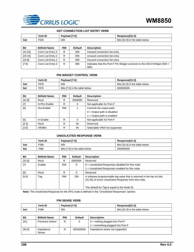
WM8850
198 Rev 4.0
GET CONNECTION LIST ENTRY VERB
Verb ID Payload [7:0] Response[31:0]
Get F02h 00h Bits [31:0] in the table below
Bit Bitfield Name RW Default Description
[31:24] Conn List Entry 3 R 00h Unused connection list entry
[23:16] Conn List Entry 2 R 00h Unused connection list entry
[15:8] Conn List Entry 1 R 00h Unused connection list entry
[7:0] Conn List Entry 0 R 08h Indicates that the Port-F Pin Widget connects to the DAC3 Widget (NID =
08h)
PIN WIDGET CONTROL VERB
Verb ID Payload [7:0] Response[31:0]
Get F07h 00h Bits [31:0] in the table below
Set 707h Bits [7:0] in the table below 00000000h
Bit Bitfield Name RW Default Description
[31:8] Rsvd R 000000h Reserved
[7] H-Phn Enable R 0 Not applicable for Port-F
[6] Out Enable RW 1 Controls the output path:
0 = Output path is disabled
1 = Output path is enabled
[5] In Enable R 0 Not applicable for Port-F
[4:3] Rsvd R 0h Reserved
[2:0] VRefEn R 0h Selectable VRef not supported
UNSOLICITED RESPONSE VERB
Verb ID Payload [7:0] Response[31:0]
Get F08h 00h Bits [31:0] in the table below
Set 708h Bits [7:0] in the table below 00000000h
Bit Bitfield Name RW Default Description
[31:8] Rsvd R 000000h Reserved
[7] Enable RW 0 0 = Unsolicited Responses disabled for this node
1 = Unsolicited Responses enabled for this node
[6] Rsvd R 0 Reserved
[5:0] Tag RW 13h A software programmable tag value that is returned in the top six bits
(31:26) of every Unsolicited Response from this node.
The default for Tag is equal to the Node ID.
Note: The Unsolicited Response for the AFG node is defined in the “Unsolicited Responses” section.
PIN SENSE VERB
Verb ID Payload [7:0] Response[31:0]
Get F09h 00h Bits [31:0] in the table below
Bit Bitfield Name RW Default Description
[31] Presence Detect R 0 0 = nothing plugged into Port-F
1 = something plugged into Port-F
[30:0] Impedance
Sense
R 00000000h Impedance sense not supported

WM8850
Rev 4.0 199
00h
01h
02h
03h
04h
05h
06h
07h
08h
09h
0Ah
0Bh
0Ch
0Dh
0Eh
0Fh
10h
11h
12h
13h
14h
15h
16h
17h
CONFIGURATION DEFAULT VERB
Verb ID Payload [7:0] Response[31:0]
Get F1Ch 00h Bits [31:0] in the table below
Set1 71Ch Bits [7:0] in the table below 00000000h
Set2 71Dh Bits [15:8] in the table below 00000000h
Set3 71Eh Bits [23:16] in the table below 00000000h
Set4 71Fh Bits [31:24] in the table below 00000000h
Bit Bitfield Name RW Default Description
[31:30] Port Connectivity RW 0h Indicates the external connectivity:
0h = Jack
1h = No physical connection
2h = A fixed function device
3h = both a jack and an internal device are connected
[29:28] Location[5:4] RW 0h Gross physical location of the device connected to Port-F:
0h = External on primary chassis
1h = Internal
2h = Separate chassis
3h = Other
[27:24] Location[3:0] RW 1h Geometric location of the device connected to Port-F:
0h = Not applicable
1h = Rear
2h = Front
3h = Left
4h = Right
5h = Top
6h = Bottom
7h = Special
8h = Special
9h = Special
Ah-Fh = Reserved
[23:20] Default Device RW 0h Indicates the intended use of Port-F:
0h = Line out
1h = Speaker
2h = Headphone out
3h = CD
4h = S/PDIF out
5h = Digital other out
6h = Modem line side
7h= Modem handset side
8h = Line in
9h = AUX
Ah = Mic in
Bh = Telephony
Ch = S/PDIF in
Dh = Digital other in
Eh = Reserved
Fh = Other

WM8850
200 Rev 4.0
Bit Bitfield Name RW Default Description
[19:16] Connection Type RW 1h Indicates the type of physical interface on Port-F:
0h = Unknown
1h = 3.5mm stereo/mono jack
2h = ¼” stereo/mono jack
3h = ATAPI internal
4h = RCA jack (for analogue audio or coaxial S/PDIF)
5h = Optical
6h = Other digital
7h = Other analogue
8h = Multi-channel analogue (DIN)
9h = XLR/Professional
Ah = RJ-11 (modem)
Bh = Combination
Ch-Eh = Reserved
Fh = Other
[15:12] Colour RW 1h Indicates the colour of the physical jack on Port-F:
0h = Unknown
1h = Black
2h = Grey
3h = Blue
4h = Green
5h = Red
6h = Orange
7h = Yellow
8h = Purple
9h = Pink
Ah-Dh = Reserved
Eh = White
Fh = Other
[11:8] Misc RW 0h Presence detection override:
0 = Presence detection indicated by Pin Capabilities Parameter (0Ch)
1 = Presence detection not supported. If the Pin Capabilities Parameter
(0Ch) indicates that that presence detection is supported by the node, then
this bit is used to override it to indicate the external circuitry is not capable
of supporting presence detect
All other values are reserved
[7:4] Default
Association
RW 2h Association number:
0h = Reserved
1h-Eh = Multi Channel or Single Pin Widget
Fh = Single Pin Widget Only
[3:0] Sequence RW 2h Sequence number used to define individual channel pairs within a stream.
All values (0h-Fh) are available for use. Use a value of 0h for Single Pin
Widget.
Note: The Configuration Default Verb is not reset to its default value during a reset from any source. The settings are only lost
when digital power is removed from the WM8850. When digital power is restored, the System BIOS must restore the settings.
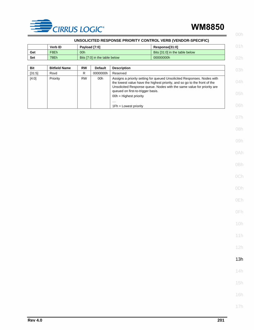
WM8850
Rev 4.0 201
00h
01h
02h
03h
04h
05h
06h
07h
08h
09h
0Ah
0Bh
0Ch
0Dh
0Eh
0Fh
10h
11h
12h
13h
14h
15h
16h
17h
UNSOLICITED RESPONSE PRIORITY CONTROL VERB (VENDOR-SPECIFIC)
Verb ID Payload [7:0] Response[31:0]
Get F8Eh 00h Bits [31:0] in the table below
Set 78Eh Bits [7:0] in the table below 00000000h
Bit Bitfield Name RW Default Description
[31:5] Rsvd R 0000000h Reserved
[4:0] Priority RW 00h Assigns a priority setting for queued Unsolicited Responses. Nodes with
the lowest value have the highest priority, and so go to the front of the
Unsolicited Response queue. Nodes with the same value for priority are
queued on first-to-trigger basis.
00h = Highest priority
…
1Fh = Lowest priority

WM8850
202 Rev 4.0

WM8850
Rev 4.0 203
00h
01h
02h
03h
04h
05h
06h
07h
08h
09h
0Ah
0Bh
0Ch
0Dh
0Eh
0Fh
10h
11h
12h
13h
14h
15h
16h
17h
BEEP GENERATOR WIDGET (NID = 14H)
AMPLIFIER GAIN/MUTE VERB
Verb ID Payload [15:0] Response[31:0]
Get Bh A000h Bits [31:0] in the response table below –
applies to the left channel only
Get Bh 8000h Bits [31:0] in the response table below –
applies to the right channel only
Set 3h Bits [15:0] in the set table below 00000000h
Response Table:
Bit Bitfield Name RW Default Description
[31:7] Rsvd R 000000h Reserved
[6:0] Amplifier Gain R 04h Shows the amplifier gain setting (step number) for the selected channel.
The actual gain applied is determined by the Output Amplifier Capabilities
Parameter, and is shown below for convenience:
00h = −24dB
01h = −18dB
02h = −12dB
03h = −6dB
04h = 0dB
Set Table:
Bit Bitfield Name RW Default Description
[15] Set Output Amp W 1 Indicates that the programming refers to the output amplifier on this
widget
[14] Set Input Amp W 0 Not applicable to this widget
[13] Set Left Amp W 1 0 = Left channel amplifier does not accept the values in Mute or Gain
fields
1 = Left channel amplifier does accept the values in the Mute and Gain
fields
[12] Set Right Amp W 1 0 = Right channel amplifier does not accept the values in Mute or Gain
fields
1 = Right channel amplifier does accept the values in the Mute and Gain
fields
[11:8] Index W 0 Not applicable to this widget
[7] Mute R 1 Mute not supported
[6:0] Gain W 4h Step number of the gain – see Amplifier Gain in response table above for
details of actual gain values
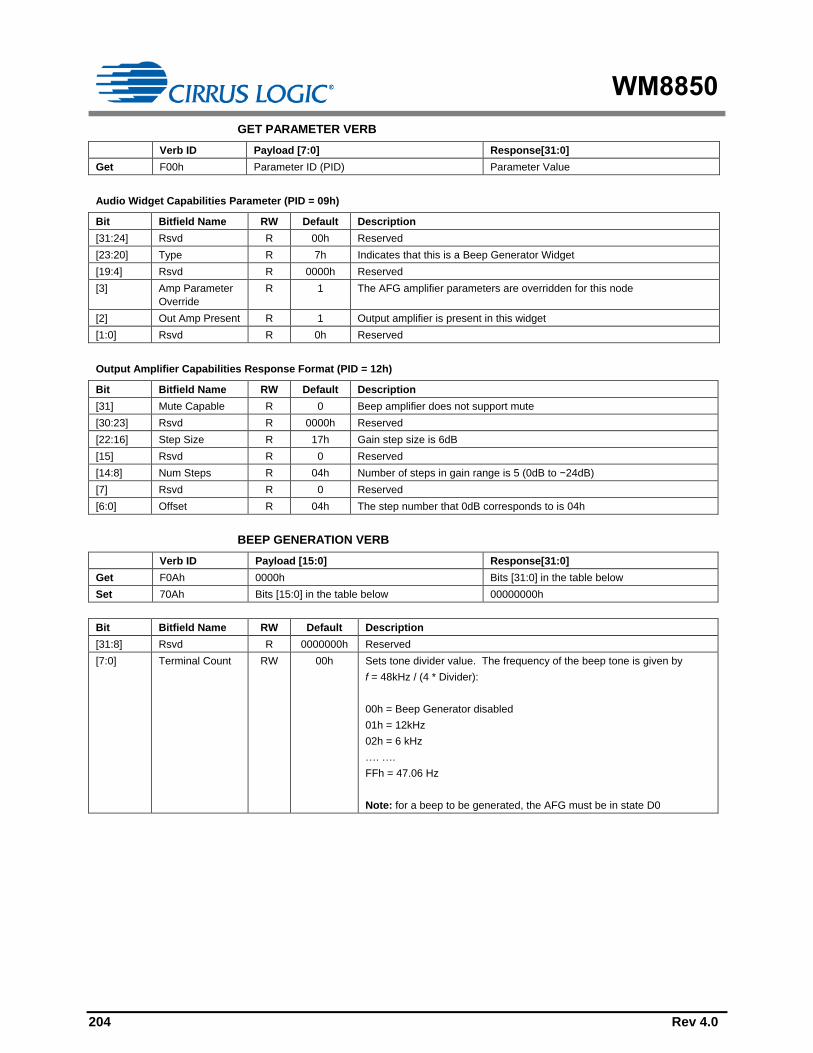
WM8850
204 Rev 4.0
GET PARAMETER VERB
Verb ID Payload [7:0] Response[31:0]
Get F00h Parameter ID (PID) Parameter Value
Audio Widget Capabilities Parameter (PID = 09h)
Bit Bitfield Name RW Default Description
[31:24] Rsvd R 00h Reserved
[23:20] Type R 7h Indicates that this is a Beep Generator Widget
[19:4] Rsvd R 0000h Reserved
[3] Amp Parameter
Override
R 1 The AFG amplifier parameters are overridden for this node
[2] Out Amp Present R 1 Output amplifier is present in this widget
[1:0] Rsvd R 0h Reserved
Output Amplifier Capabilities Response Format (PID = 12h)
Bit Bitfield Name RW Default Description
[31] Mute Capable R 0 Beep amplifier does not support mute
[30:23] Rsvd R 0000h Reserved
[22:16] Step Size R 17h Gain step size is 6dB
[15] Rsvd R 0 Reserved
[14:8] Num Steps R 04h Number of steps in gain range is 5 (0dB to −24dB)
[7] Rsvd R 0 Reserved
[6:0] Offset R 04h The step number that 0dB corresponds to is 04h
BEEP GENERATION VERB
Verb ID Payload [15:0] Response[31:0]
Get F0Ah 0000h Bits [31:0] in the table below
Set 70Ah Bits [15:0] in the table below 00000000h
Bit Bitfield Name RW Default Description
[31:8] Rsvd R 0000000h Reserved
[7:0] Terminal Count RW 00h Sets tone divider value. The frequency of the beep tone is given by
f = 48kHz / (4 * Divider):
00h = Beep Generator disabled
01h = 12kHz
02h = 6 kHz
…. ….
FFh = 47.06 Hz
Note: for a beep to be generated, the AFG must be in state D0
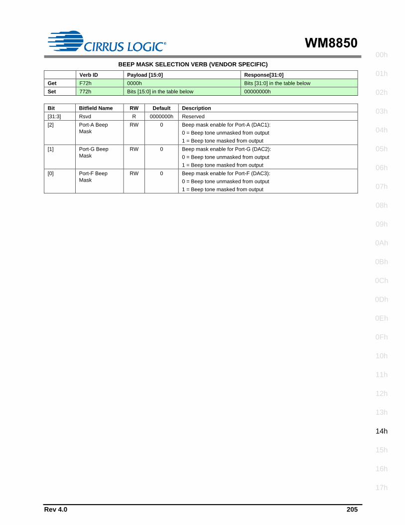
WM8850
Rev 4.0 205
00h
01h
02h
03h
04h
05h
06h
07h
08h
09h
0Ah
0Bh
0Ch
0Dh
0Eh
0Fh
10h
11h
12h
13h
14h
15h
16h
17h
BEEP MASK SELECTION VERB (VENDOR SPECIFIC)
Verb ID Payload [15:0] Response[31:0]
Get F72h 0000h Bits [31:0] in the table below
Set 772h Bits [15:0] in the table below 00000000h
Bit Bitfield Name RW Default Description
[31:3] Rsvd R 0000000h Reserved
[2] Port-A Beep
Mask
RW 0 Beep mask enable for Port-A (DAC1):
0 = Beep tone unmasked from output
1 = Beep tone masked from output
[1] Port-G Beep
Mask
RW 0 Beep mask enable for Port-G (DAC2):
0 = Beep tone unmasked from output
1 = Beep tone masked from output
[0] Port-F Beep
Mask
RW 0 Beep mask enable for Port-F (DAC3):
0 = Beep tone unmasked from output
1 = Beep tone masked from output

WM8850
206 Rev 4.0
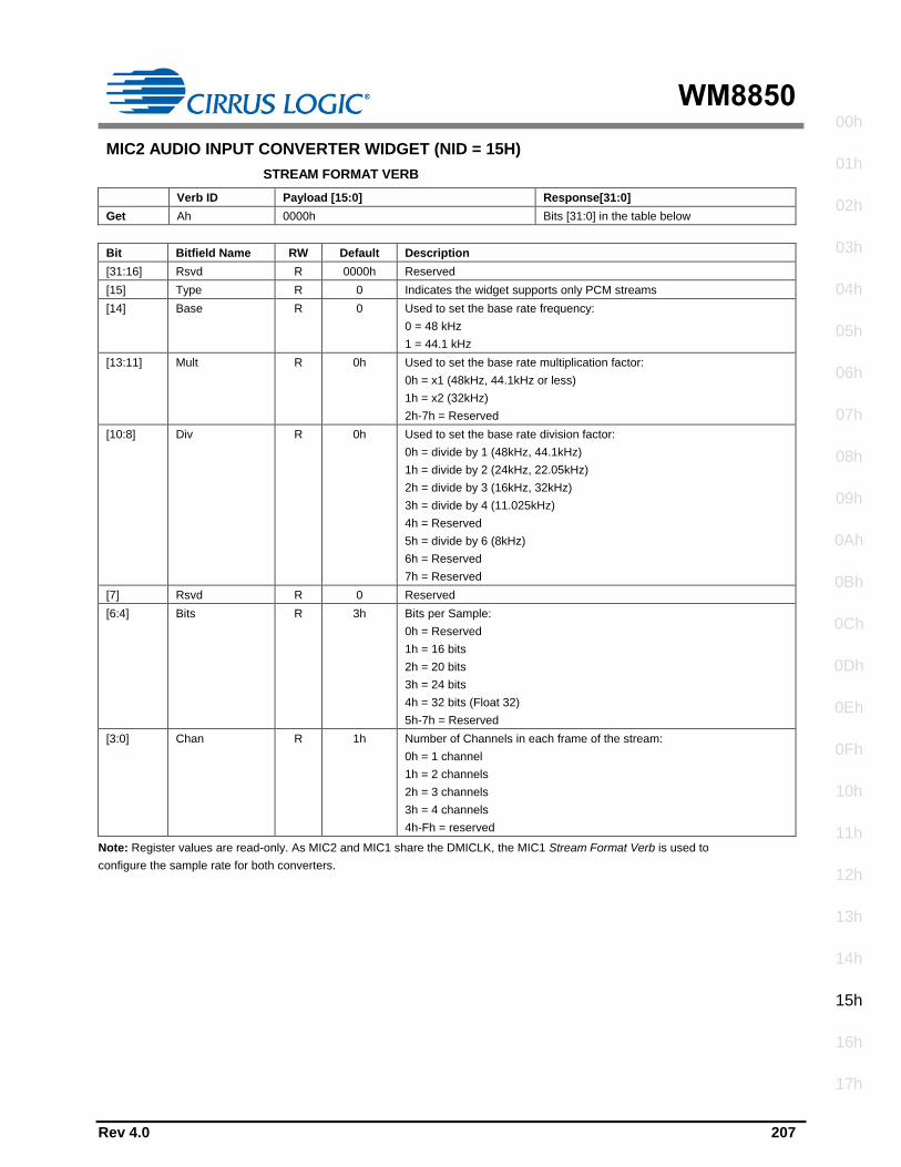
WM8850
Rev 4.0 207
00h
01h
02h
03h
04h
05h
06h
07h
08h
09h
0Ah
0Bh
0Ch
0Dh
0Eh
0Fh
10h
11h
12h
13h
14h
15h
16h
17h
MIC2 AUDIO INPUT CONVERTER WIDGET (NID = 15H)
STREAM FORMAT VERB
Verb ID Payload [15:0] Response[31:0]
Get Ah 0000h Bits [31:0] in the table below
Bit Bitfield Name RW Default Description
[31:16] Rsvd R 0000h Reserved
[15] Type R 0 Indicates the widget supports only PCM streams
[14] Base R 0 Used to set the base rate frequency:
0 = 48 kHz
1 = 44.1 kHz
[13:11] Mult R 0h Used to set the base rate multiplication factor:
0h = x1 (48kHz, 44.1kHz or less)
1h = x2 (32kHz)
2h-7h = Reserved
[10:8] Div R 0h Used to set the base rate division factor:
0h = divide by 1 (48kHz, 44.1kHz)
1h = divide by 2 (24kHz, 22.05kHz)
2h = divide by 3 (16kHz, 32kHz)
3h = divide by 4 (11.025kHz)
4h = Reserved
5h = divide by 6 (8kHz)
6h = Reserved
7h = Reserved
[7] Rsvd R 0 Reserved
[6:4] Bits R 3h Bits per Sample:
0h = Reserved
1h = 16 bits
2h = 20 bits
3h = 24 bits
4h = 32 bits (Float 32)
5h-7h = Reserved
[3:0] Chan R 1h Number of Channels in each frame of the stream:
0h = 1 channel
1h = 2 channels
2h = 3 channels
3h = 4 channels
4h-Fh = reserved
Note: Register values are read-only. As MIC2 and MIC1 share the DMICLK, the MIC1 Stream Format Verb is used to
configure the sample rate for both converters.

WM8850
208 Rev 4.0
GET PARAMETER VERB
Verb ID Payload [7:0] Response[31:0]
Get F00h Parameter ID (PID) Parameter Value
Audio Widget Capabilities Parameter (PID = 09h)
Bit Bitfield Name RW Default Description
[31:24] Rsvd R 00h Reserved
[23:20] Type R 1h Indicates that this is an Audio Input Widget
[19:16] Delay R 0h Latency not reported
[15:12] Rsvd R 0h Reserved
[11] L-R Swap R 0 Left/Right swap capability not supported
[10] PowerCntrl R 0 Indicates that the Power State Verb is not supported in this widget
[9] Digital R 1 Indicates that this widget is translating digital data
[8] Conn List R 1 Indicates that a connection list is present
[7] Unsol Capable R 1 Widget supports Unsolicited Responses
[6] ProcWidget R 1 Widget has processing capabilities (i.e high pass filter)
[5] Stripe R 0 Widget does not support striping
[4] Format Override R 1 Widget has a subset of the supported rates defined for the AFG
[3] Amp Parameter
Override
R 0 Not applicable as this widget does not have amplifier capabilities
[2] Out Amp Present R 0 Output amplifier not applicable for this widget
[1] In Amp Present R 0 Input amplifier not present in this widget
[0] Stereo R 1 Indicates that this is a stereo widget
Supported Rates Parameter (PID = 0Ah)
Bit Bitfield Name RW Default Description
[31:21] Rsvd R 000h Reserved
[20] B32 R 1 MIC1 supports 32-bit audio format
[19] B24 R 1 MIC1 supports 24-bit audio format
[18] B20 R 1 MIC1 supports 20-bit audio format
[17] B16 R 1 MIC1 supports 16-bit audio format
[16] B8 R 0 MIC1 does not support 8-bit audio format
[15:12] Rsvd R 0h Reserved
[11] R12 R 0 MIC1 does not support 384 kHz sample rate
[10] R11 R 0 MIC1 does not support 192 kHz sample rate
[9] R10 R 0 MIC1 does not support 176.4 kHz sample rate
[8] R9 R 0 MIC1 does not support 96 kHz sample rate
[7] R8 R 0 MIC1 does not support 88.2 kHz sample rate
[6] R7 R 1 MIC1 supports 48 kHz sample rate
[5] R6 R 1 MIC1 supports 44.1 kHz sample rate
[4] R5 R 1 MIC1 supports 32 kHz sample rate
[3] R4 R 1 MIC1 supports 22.05 kHz sample rate
[2] R3 R 1 MIC1 supports 16 kHz sample rate
[1] R2 R 1 MIC1 supports 11.025 kHz sample rate
[0] R1 R 1 MIC1 supports 8 kHz sample rate
Supported Stream Formats Parameter (PID = 0Bh)
Bit Bitfield Name RW Default Description
[31:3] Rsvd R 00000000h Reserved
[2] AC3 R 0 MIC2 does not support Dolby AC3 formatted data
[1] Float32 R 1 MIC2 supports Float32 formatted data
[0] PCM R 1 MIC2 supports PCM formatted data

WM8850
Rev 4.0 209
00h
01h
02h
03h
04h
05h
06h
07h
08h
09h
0Ah
0Bh
0Ch
0Dh
0Eh
0Fh
10h
11h
12h
13h
14h
15h
16h
17h
Connection List Length Parameter (PID = 0Eh)
Bit Bitfield Name RW Default Description
[31:8] Rsvd R 000000h Reserved
[7] Long Form R 0 Indicates that the connection list items are in short form
[6:0] Connection List
Length
R 01h Indicates that there is 1 NID entry in the connection list
Processing Capabilities Parameter (PID = 10h)
Bit Bitfield Name RW Default Description
[31:16] Rsvd R 0000h Reserved
[15:8] NumCoeff R 00h This widget does not support loadable coefficients
[7:1] Rsvd R 00h Reserved
[0] Benign R 0 The “Processing Benign State” is not supported
GET CONNECTION LIST ENTRY VERB
Verb ID Payload [7:0] Response[31:0]
Get F02h 00h Bits [31:0] in the table below
Bit Bitfield Name RW Default Description
[31:24] Conn List Entry 3 R 00h Unused connection list entry
[23:16] Conn List Entry 2 R 00h Unused connection list entry
[15:8] Conn List Entry 1 R 00h Unused connection list entry
[7:0] Conn List Entry 0 R 16h Indicates that the MIC2 Widget connects to the Port-H Pin Widget (NID =
16h)
PROCESSING STATE VERB
Verb ID Payload [7:0] Response[31:0]
Get F03h 00h Bits [31:0] in the table below
Set 703h Bits [7:0] in the table below 00000000h
Bit Bitfield Name RW Default Description
[31:8] Rsvd R 000000h Reserved
[7:0] Processing State RW 01h The processing block is the high-pass filter (HPF). The processing state
is controlled as follows:
00h = Processing Off: HPF disabled
01h = Processing On: HPF enabled
02h = Processing Off: HPF disabled (benign not supported)
03h-7Fh = Reserved
80h-FFh = Vendor Specific – not used

WM8850
210 Rev 4.0
CONVERTER STREAM, CHANNEL VERB
Verb ID Payload [7:0] Response[31:0]
Get F06h 00h Bits [31:0] in the table below
Set 706h Bits [7:0] in the table below 00000000h
Bit Bitfield Name RW Default Description
[31:8] Rsvd R 000000h Reserved
[7:4] Stream RW 0h Stream ID used by this widget. Note that Stream ID = 0h is used to indicate
an unused stream, and converters will not transfer/receive link data for
streams with an ID of 0h.
For multi-channel capture on MIC1 and MIC2, the Stream value should be
the same for both.
[3:0] Channel RW 2h Lowest channel number used by this widget.
Note: When MIC1 and MIC2 are setup for multi-channel capture, only a
setting of 0h and 2h are applicable. However, the values are mutually
exclusive, in that if Channel has been set to 0h for the MIC1 node, it must
be set to 2h for the MIC2 node. Both nodes should have Channel set to 0h
when not in multi-channel capture mode.
UNSOLICITED RESPONSE VERB
Verb ID Payload [7:0] Response[31:0]
Get F08h 00h Bits [31:0] in the table below
Set 708h Bits [7:0] in the table below 00000000h
Bit Bitfield Name RW Default Description
[31:8] Rsvd R 000000h Reserved
[7] Enable RW 0h 0 = Unsolicited Responses disabled for this node
1 = Unsolicited Responses enabled for this node
[6] Rsvd R 0h Reserved
[5:0] Tag RW 15h A software programmable tag value that is returned in the top six bits
(31:26) of every Unsolicited Response from this node.
The default for Tag is equal to the Node ID.
Note: The Unsolicited Response for the AFG node is defined in the “Unsolicited Responses” section.
UNSOLICITED RESPONSE PRIORITY CONTROL VERB (VENDOR-SPECIFIC)
Verb ID Payload [7:0] Response[31:0]
Get F8Eh 00h Bits [31:0] in the table below
Set 78Eh Bits [7:0] in the table below 00000000h
Bit Bitfield Name RW Default Description
[31:5] Rsvd R 0000000h Reserved
[4:0] Priority RW 00h Assigns a priority setting for queued Unsolicited Responses. Nodes with
the lowest value have the highest priority, and so go to the front of the
Unsolicited Response queue. Nodes with the same value for priority are
queued on first-to-trigger basis.
00h = Highest priority
…
1Fh = Lowest priority
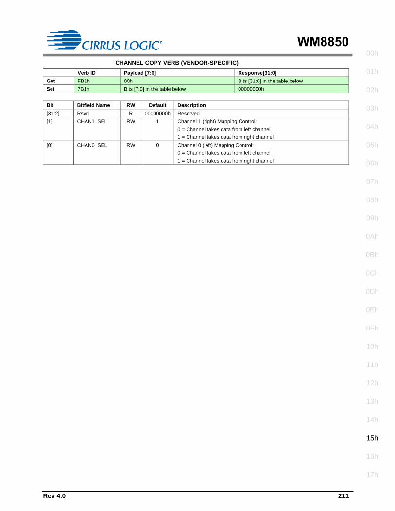
WM8850
Rev 4.0 211
00h
01h
02h
03h
04h
05h
06h
07h
08h
09h
0Ah
0Bh
0Ch
0Dh
0Eh
0Fh
10h
11h
12h
13h
14h
15h
16h
17h
CHANNEL COPY VERB (VENDOR-SPECIFIC)
Verb ID Payload [7:0] Response[31:0]
Get FB1h 00h Bits [31:0] in the table below
Set 7B1h Bits [7:0] in the table below 00000000h
Bit Bitfield Name RW Default Description
[31:2] Rsvd R 00000000h Reserved
[1] CHAN1_SEL RW 1 Channel 1 (right) Mapping Control:
0 = Channel takes data from left channel
1 = Channel takes data from right channel
[0] CHAN0_SEL RW 0 Channel 0 (left) Mapping Control:
0 = Channel takes data from left channel
1 = Channel takes data from right channel

WM8850
212 Rev 4.0

WM8850
Rev 4.0 213
00h
01h
02h
03h
04h
05h
06h
07h
08h
09h
0Ah
0Bh
0Ch
0Dh
0Eh
0Fh
10h
11h
12h
13h
14h
15h
16h
17h
PORT-H PIN COMPLEX WIDGET (NID = 16H)
AMPLIFIER GAIN/MUTE VERB
Verb ID Payload [15:0] Response[31:0]
Get Bh 2000h Bits [31:0] in the response table below –
applies to the left channel only
Get Bh 0000h Bits [31:0] in the response table below –
applies to the right channel only
Set 3h Bits [7:0] in the set table below 00000000h
Response Table:
Bit Bitfield Name RW Default Description
[31:8] Rsvd R 000000h Reserved
[7] Amplifier Mute R 0 Shows the amplifier mute status of the selected channel:
0 = Normal
1 = Muted
[6:0] Amplifier Gain R 18h Shows the amplifier gain setting (step number) for the selected channel.
The actual gain applied is determined by the Input Amplifier Capabilities
Parameter in the AFG (NID = 01h), and is shown below for convenience:
00h = −12dB
01h = −11.5dB
… −0.5dB steps
57h = +31.5dB
58h = +32dB
Set Table:
Bit Bitfield Name RW Default Description
[15] Set Output Amp W 0 Not applicable to this widget
[14] Set Input Amp W 1 Indicates that the programming refers to the input amplifier on this widget
[13] Set Left Amp W 1 0 = Left channel amplifier does not accept the values in Mute or Gain
fields
1 = Left channel amplifier does accept the values in the Mute and Gain
fields
[12] Set Right Amp W 1 0 = Right channel amplifier does not accept the values in Mute or Gain
fields
1 = Right channel amplifier does accept the values in the Mute and Gain
fields
[11:8] Index W 0h Not applicable to this widget
[7] Mute W 0 0 = Normal operation
1 = Mute
[6:0] Gain W 18h Step number of the gain – see Amplifier Gain in response table above for
details of actual gain values

WM8850
214 Rev 4.0
GET PARAMETER VERB
Verb ID Payload [7:0] Response[31:0]
Get F00h Parameter ID (PID) Parameter Value
Audio Widget Capabilities Parameter (PID = 09h)
Bit Bitfield Name RW Default Description
[31:24] Rsvd R 00h Reserved
[23:20] Type R 4h Indicates that this is a Pin Complex Widget
[19:16] Delay R 0h Latency not reported
[15:12] Rsvd R 0h Reserved
[11] L-R Swap R 0 Left/Right swap capability not supported
[10] PowerCntrl R 0 Indicates that the Power State Verb is not supported in this widget
[9] Digital R 1 Indicates that this widget is translating digital data
[8] Conn List R 1 Indicates that a connection list is present
[7] Unsol Capable R 0 Widget does not support Unsolicited Responses
[6] ProcWidget R 0 Widget does not have processing capabilities
[5] Stripe R 0 Widget does not support striping
[4] Format Override R 0 Widget does not override the format defined for the AFG
[3] Amp Parameter
Override
R 1 The AFG amplifier parameters are overridden for this node
[2] Out Amp Present R 0 Output amplifier not present in this widget
[1] In Amp Present R 1 Input amplifier is present in this widget
[0] Stereo R 1 Indicates that this is a stereo widget
Pin Capabilities Parameter (PID = 0Ch)
Bit Bitfield Name RW Default Description
[31:17] Rsvd R 0000h Reserved
[16] EAPD Capable R 0 Widget does not support an EAPD pin
[15:8] VRef Control R 00h VRef not supported for digital inputs
[7] Rsvd R 0 Reserved
[6] Balanced I/O
Pins
R 0 Indicates that this widget does not have balanced pins
[5] Input Capable R 1 Indicates that this widget is input capable
[4] Output Capable R 1 Indicates that this widget is output capable
[3] Headphone
Drive Capable
R 0 Not applicable as this in an input port
[2] Presence Detect
Capable
R 0 Presence detection not supported
[1] Trigger Required R 0 Impedance measurement not supported
[0] Impedance
Sense Capable
R 0 Impedance measurement not supported
Input Amplifier Capabilities Response Format (PID = 0Dh)
Bit Bitfield Name RW Default Description
[31] Mute Capable R 1 DMIC Amplifiers are capable of hard-mute
[30:23] Rsvd R 00h Reserved
[22:16] Step Size R 01h Gain step size is 0.5dB
[15] Rsvd R 0 Reserved
[14:8] Num Steps R 58h Number of steps in gain range is 89 (−12dB to +32dB)
[7] Rsvd R 0 Reserved
[6:0] Offset R 18h The step number that 0dB corresponds to is 18h

WM8850
Rev 4.0 215
00h
01h
02h
03h
04h
05h
06h
07h
08h
09h
0Ah
0Bh
0Ch
0Dh
0Eh
0Fh
10h
11h
12h
13h
14h
15h
16h
17h
Connection List Length Parameter (PID = 0Eh)
Bit Bitfield Name RW Default Description
[31:8] Rsvd R 000000h Reserved
[7] Long Form R 0 Indicates that the connection list items are in short form
[6:0] Connection List
Length
R 01h Indicates that there is 1 NID entry in the connection list
GET CONNECTION LIST ENTRY VERB
Verb ID Payload [7:0] Response[31:0]
Get F02h 00h Bits [31:0] in the table below
Bit Bitfield Name RW Default Description
[31:24] Conn List Entry 3 R 00h Unused connection list entry
[23:16] Conn List Entry 2 R 00h Unused connection list entry
[15:8] Conn List Entry 1 R 00h Unused connection list entry
[7:0] Conn List Entry 0 R 17h Indicates that the Port-H Pin Widget connects to the S/PDIF Tx 2 Widget
(NID = 17h)
PIN WIDGET CONTROL VERB
Verb ID Payload [7:0] Response[31:0]
Get F07h 00h Bits [31:0] in the table below
Set 707h Bits [7:0] in the table below 00000000h
Bit Bitfield Name RW Default Description
[31:8] Rsvd R 000000h Reserved
[7] H-Phn Enable R 0 Not applicable as this in an input port
[6] Out Enable RW 0 Controls the output path:
0 = Output path is disabled
1 = Output path is enabled
[5] In Enable RW 1 Controls the input path:
0 = Input path is disabled
1 = Input path is enabled
[4:3] Rsvd R 0h Reserved
[2:0] VRefEn R 0h Selectable VRef not supported
Note: It is erroneous behaviour for both the Out Enable and In Enable registers to be set high simultaneously. If both registers
are set, Port-H defaults to an input.
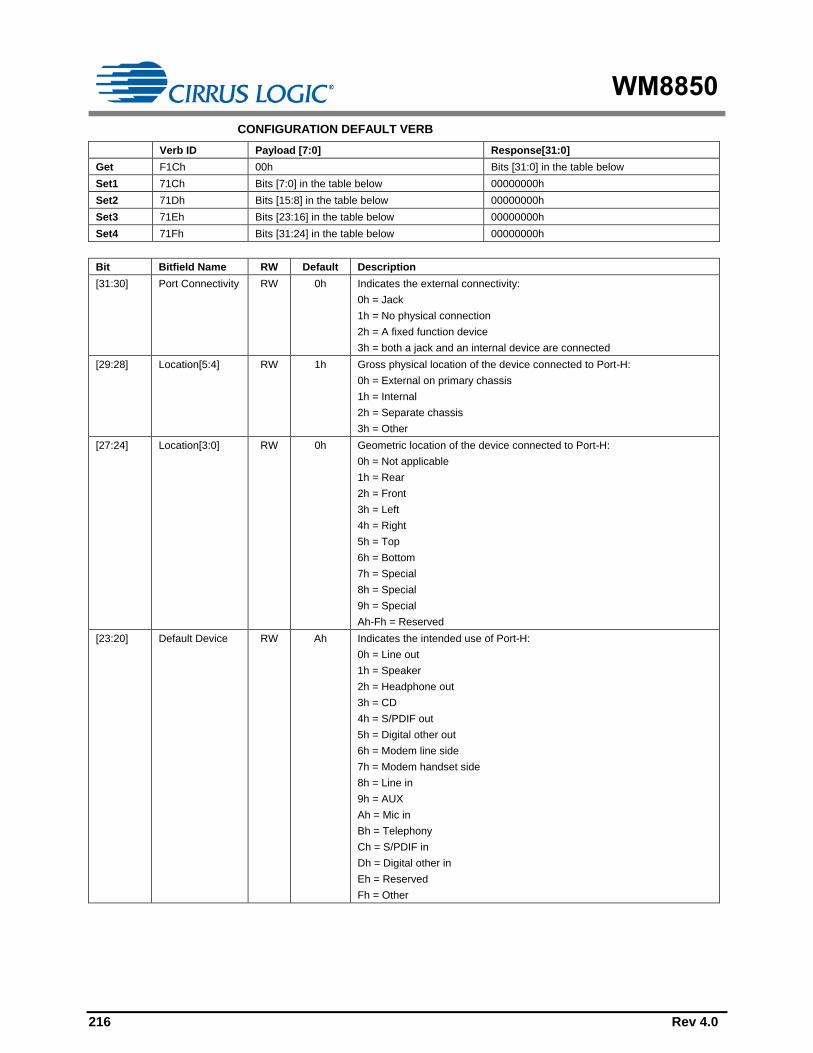
WM8850
216 Rev 4.0
CONFIGURATION DEFAULT VERB
Verb ID Payload [7:0] Response[31:0]
Get F1Ch 00h Bits [31:0] in the table below
Set1 71Ch Bits [7:0] in the table below 00000000h
Set2 71Dh Bits [15:8] in the table below 00000000h
Set3 71Eh Bits [23:16] in the table below 00000000h
Set4 71Fh Bits [31:24] in the table below 00000000h
Bit Bitfield Name RW Default Description
[31:30] Port Connectivity RW 0h Indicates the external connectivity:
0h = Jack
1h = No physical connection
2h = A fixed function device
3h = both a jack and an internal device are connected
[29:28] Location[5:4] RW 1h Gross physical location of the device connected to Port-H:
0h = External on primary chassis
1h = Internal
2h = Separate chassis
3h = Other
[27:24] Location[3:0] RW 0h Geometric location of the device connected to Port-H:
0h = Not applicable
1h = Rear
2h = Front
3h = Left
4h = Right
5h = Top
6h = Bottom
7h = Special
8h = Special
9h = Special
Ah-Fh = Reserved
[23:20] Default Device RW Ah Indicates the intended use of Port-H:
0h = Line out
1h = Speaker
2h = Headphone out
3h = CD
4h = S/PDIF out
5h = Digital other out
6h = Modem line side
7h = Modem handset side
8h = Line in
9h = AUX
Ah = Mic in
Bh = Telephony
Ch = S/PDIF in
Dh = Digital other in
Eh = Reserved
Fh = Other
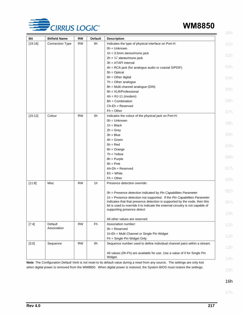
WM8850
Rev 4.0 217
00h
01h
02h
03h
04h
05h
06h
07h
08h
09h
0Ah
0Bh
0Ch
0Dh
0Eh
0Fh
10h
11h
12h
13h
14h
15h
16h
17h
Bit Bitfield Name RW Default Description
[19:16] Connection Type RW 6h Indicates the type of physical interface on Port-H:
0h = Unknown
1h = 3.5mm stereo/mono jack
2h = ¼” stereo/mono jack
3h = ATAPI internal
4h = RCA jack (for analogue audio or coaxial S/PDIF)
5h = Optical
6h = Other digital
7h = Other analogue
8h = Multi-channel analogue (DIN)
9h = XLR/Professional
Ah = RJ-11 (modem)
Bh = Combination
Ch-Eh = Reserved
Fh = Other
[15:12] Colour RW 0h Indicates the colour of the physical jack on Port-H:
0h = Unknown
1h = Black
2h = Grey
3h = Blue
4h = Green
5h = Red
6h = Orange
7h = Yellow
8h = Purple
9h = Pink
Ah-Dh = Reserved
Eh = White
Fh = Other
[11:8] Misc RW 1h Presence detection override:
0h = Presence detection indicated by Pin Capabilities Parameter
1h = Presence detection not supported. If the Pin Capabilities Parameter
indicates that that presence detection is supported by the node, then this
bit is used to override it to indicate the external circuitry is not capable of
supporting presence detect
All other values are reserved
[7:4] Default
Association
RW Fh Association number:
0h = Reserved
1h-Eh = Multi Channel or Single Pin Widget
Fh = Single Pin Widget Only
[3:0] Sequence RW 0h Sequence number used to define individual channel pairs within a stream.
All values (0h-Fh) are available for use. Use a value of 0 for Single Pin
Widget.
Note: The Configuration Default Verb is not reset to its default value during a reset from any source. The settings are only lost
when digital power is removed from the WM8850. When digital power is restored, the System BIOS must restore the settings.

WM8850
218 Rev 4.0
INTERNAL PATH VERB (VENDOR-SPECIFIC)
Verb ID Payload [7:0] Response[31:0]
Get F73h 00h Bits [31:0] in the table below
Set 773h Bits [7:0] in the table below 00000000h
Bit Bitfield Name RW Default Description
[31:8] Rsvd R 00000000h Reserved
[7:0] Path Sel RW 17h Selects source of Port-H node:
10h = Use data from SPDIF_IN (NID=10h)
17h = Use data from S/PDIF Tx2 (NID=17h)

WM8850
Rev 4.0 219
00h
01h
02h
03h
04h
05h
06h
07h
08h
09h
0Ah
0Bh
0Ch
0Dh
0Eh
0Fh
10h
11h
12h
13h
14h
15h
16h
17h
S/PDIF TX 2 AUDIO OUTPUT CONVERTER WIDGET (NID = 17H)
STREAM FORMAT VERB
Verb ID Payload [15:0] Response[31:0]
Get Ah 0000h Bits [31:0] in the table below
Set 2h Bits [15:0] in the table below 00000000h
Bit Bitfield Name RW Default Description
[31:16] Rsvd R 0000h Reserved
[15] Type RW 0 Used to set the format of the stream:
0 = PCM
1 = Non-PCM (i.e. AC3 or Software Formatted S/PDIF)
[14] Base RW 0 Used to set the base rate frequency:
0h = 48 kHz
1h = 44.1 kHz
[13:11] Mult RW 0h Used to set the base rate multiplication factor:
0h = x1 (48kHz, 44.1kHz or less)
1h = x2 (96kHz, 88.2kHz, 32kHz)
2h = Reserved
3h = x4 (192kHz, 176.4kHz)
4h-7h = Reserved
[10:8] Div RW 0h Used to set the base rate division factor:
0h = divide by 1 (48kHz, 44.1kHz)
1h = Reserved
2h = divide by 3 (32kHz)
3h-7h = Reserved
[7] Rsvd R 0 Reserved
[6:4] Bits RW 4h Bits per Sample:
0h = Reserved
1h = 16 bits
2h = 20 bits
3h = 24 bits
4h = 32 bits (Software Formatted or Float 32)
5h-7h = Reserved
[3:0] Chan RW 1h Number of Channels in each frame of the stream:
0h = 1 channel
1h = 2 channels
2h-Fh = reserved
Notes:
1. When Software Formatted S/PDIF is selected, verb settings for channel status and validity are not used.
2. When Software Formatted S/PDIF is selected, the S/PDIF output is driven low until Stream ID is assigned.

WM8850
220 Rev 4.0
GET PARAMETER VERB
Verb ID Payload [7:0] Response[31:0]
Get F00h Parameter ID (PID) Parameter Value
Audio Widget Capabilities Parameter (PID = 09h)
Bit Bitfield Name RW Default Description
[31:24] Rsvd R 00h Reserved
[23:20] Type R 0h Indicates that this is an Audio Output Widget
[19:16] Delay R 0h Latency not reported
[15:12] Rsvd R 0h Reserved
[11] L-R Swap R 0 Left/Right swap capability not supported
[10] PowerCntrl R 0 Indicates that the Power State Verb is supported in this widget
[9] Digital R 1 Indicates that this widget is translating digital data
[8] Conn List R 0 Indicates that a connection list is not present
[7] Unsol Capable R 1 Widget supports Unsolicited Responses
[6] ProcWidget R 0 Widget does not have processing capabilities
[5] Stripe R 0 Widget does not support striping
[4] Format Override R 1 Widget has a subset of the supported rates defined for the AFG
[3] Amp Parameter
Override
R 0 Not applicable as this widget does not have amplifier capabilities
[2] Out Amp Present R 0 Output amplifier not present in this widget
[1] In Amp Present R 0 Input amplifier not present in this widget
[0] Stereo R 1 Indicates that this is a stereo widget
Supported Rates Parameter (PID = 0Ah)
Bit Bitfield Name RW Default Description
[31:21] Rsvd R 000h Reserved
[20] B32 R 1 Float32 and Software Formatted S/PDIFis supported.
[19] B24 R 1 S/PDIF Tx 2 supports 24-bit audio format
[18] B20 R 1 S/PDIF Tx 2 supports 20-bit audio format
[17] B16 R 1 S/PDIF Tx 2 supports 16-bit audio format
[16] B8 R 0 S/PDIF Tx 2 does not support 8-bit audio format
[15:12] Rsvd R 0h Reserved
[11] R12 R 0 S/PDIF Tx 2 does not support 384 kHz sample rate
[10] R11 R 1 S/PDIF Tx 2 supports 192 kHz sample rate
[9] R10 R 1 S/PDIF Tx 2 supports 176.4 kHz sample rate
[8] R9 R 1 S/PDIF Tx 2 supports 96 kHz sample rate
[7] R8 R 1 S/PDIF Tx 2 supports 88.2 kHz sample rate
[6] R7 R 1 S/PDIF Tx 2 supports 48 kHz sample rate
[5] R6 R 1 S/PDIF Tx 2 supports 44.1 kHz sample rate
[4] R5 R 1 S/PDIF Tx 2 supports 32 kHz sample rate
[3] R4 R 0 S/PDIF Tx 2 does not support 22.05 kHz sample rate
[2] R3 R 0 S/PDIF Tx 2 does not support 16 kHz sample rate
[1] R2 R 0 S/PDIF Tx 2 does not support 11.025 kHz sample rate
[0] R1 R 0 S/PDIF Tx 2 does not support 8 kHz sample rate
Supported Stream Formats Parameter (PID = 0Bh)
Bit Bitfield Name RW Default Description
[31:3] Rsvd R 00000000h Reserved
[2] AC3 R 0 S/PDIF Tx 2 does not support Dolby AC3 format
[1] Float32 R 1 S/PDIF Tx 2 supports Float32 formatted data
[0] PCM R 1 S/PDIF Tx 2 PCM formatted data

WM8850
Rev 4.0 221
00h
01h
02h
03h
04h
05h
06h
07h
08h
09h
0Ah
0Bh
0Ch
0Dh
0Eh
0Fh
10h
11h
12h
13h
14h
15h
16h
17h
CONVERTER STREAM, CHANNEL VERB
Verb ID Payload [7:0] Response[31:0]
Get F06h 00h Bits [31:0] in the table below
Set 706h Bits [7:0] in the table below 00000000h
Bit Bitfield Name RW Default Description
[31:8] Rsvd R 000000h Reserved
[7:4] Stream RW 0h Stream ID used by this widget. Note that Stream ID = 0h is used to indicate
an unused stream, and converters will not transfer/receive link data for
streams with an ID of 0h.
[3:0] Channel RW 0h Lowest channel number used by this widget.
Note: As this widget does not support multi-channel capture, only a setting
of 0 is applicable.
UNSOLICITED RESPONSE VERB
Verb ID Payload [7:0] Response[31:0]
Get F08h 00h Bits [31:0] in the table below
Set 708h Bits [7:0] in the table below 00000000h
Bit Bitfield Name RW Default Description
[31:8] Rsvd R 000000h Reserved
[7] Enable RW 0 0 = Unsolicited Responses disabled for this node
1 = Unsolicited Responses enabled for this node
[6] Rsvd R 0 Reserved
[5:0] Tag RW 17h A software programmable tag value that is returned in the top six bits
(31:26) of every Unsolicited Response from this node.
The default for Tag is equal to the Node ID.
Note: The Unsolicited Response for the AFG node is defined in the “Unsolicited Responses” section.
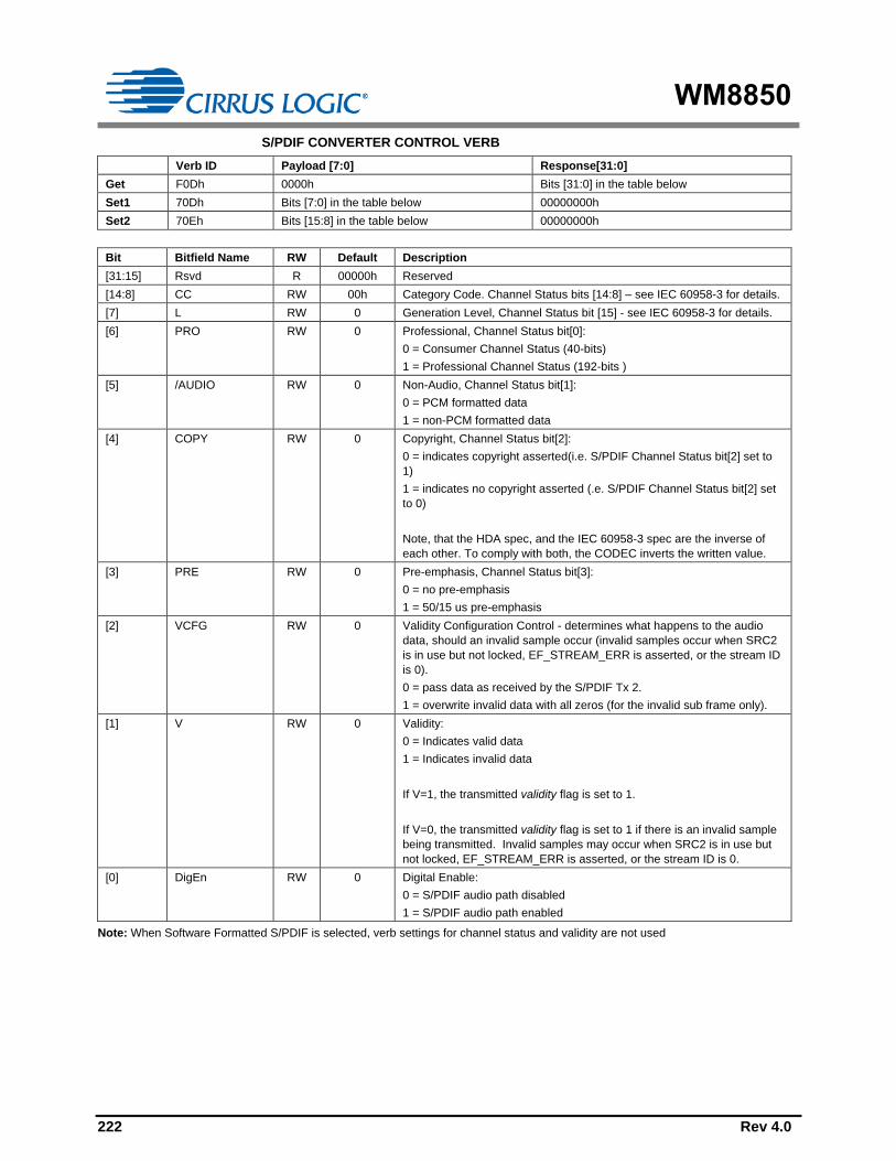
WM8850
222 Rev 4.0
S/PDIF CONVERTER CONTROL VERB
Verb ID Payload [7:0] Response[31:0]
Get F0Dh 0000h Bits [31:0] in the table below
Set1 70Dh Bits [7:0] in the table below 00000000h
Set2 70Eh Bits [15:8] in the table below 00000000h
Bit Bitfield Name RW Default Description
[31:15] Rsvd R 00000h Reserved
[14:8] CC RW 00h Category Code. Channel Status bits [14:8] – see IEC 60958-3 for details.
[7] L RW 0 Generation Level, Channel Status bit [15] - see IEC 60958-3 for details.
[6] PRO RW 0 Professional, Channel Status bit[0]:
0 = Consumer Channel Status (40-bits)
1 = Professional Channel Status (192-bits )
[5] /AUDIO RW 0 Non-Audio, Channel Status bit[1]:
0 = PCM formatted data
1 = non-PCM formatted data
[4] COPY RW 0 Copyright, Channel Status bit[2]:
0 = indicates copyright asserted(i.e. S/PDIF Channel Status bit[2] set to
1)
1 = indicates no copyright asserted (.e. S/PDIF Channel Status bit[2] set
to 0)
Note, that the HDA spec, and the IEC 60958-3 spec are the inverse of
each other. To comply with both, the CODEC inverts the written value.
[3] PRE RW 0 Pre-emphasis, Channel Status bit[3]:
0 = no pre-emphasis
1 = 50/15 us pre-emphasis
[2] VCFG RW 0 Validity Configuration Control - determines what happens to the audio
data, should an invalid sample occur (invalid samples occur when SRC2
is in use but not locked, EF_STREAM_ERR is asserted, or the stream ID
is 0).
0 = pass data as received by the S/PDIF Tx 2.
1 = overwrite invalid data with all zeros (for the invalid sub frame only).
[1] V RW 0 Validity:
0 = Indicates valid data
1 = Indicates invalid data
If V=1, the transmitted validity flag is set to 1.
If V=0, the transmitted validity flag is set to 1 if there is an invalid sample
being transmitted. Invalid samples may occur when SRC2 is in use but
not locked, EF_STREAM_ERR is asserted, or the stream ID is 0.
[0] DigEn RW 0 Digital Enable:
0 = S/PDIF audio path disabled
1 = S/PDIF audio path enabled
Note: When Software Formatted S/PDIF is selected, verb settings for channel status and validity are not used

WM8850
Rev 4.0 223
00h
01h
02h
03h
04h
05h
06h
07h
08h
09h
0Ah
0Bh
0Ch
0Dh
0Eh
0Fh
10h
11h
12h
13h
14h
15h
16h
17h
INTERNAL PATH VERB (VENDOR-SPECIFIC)
Verb ID Payload [7:0] Response[31:0]
Get F73h 00h Bits [31:0] in the table below
Set1 773h Bits [7:0] in the table below 00000000h
Bit Bitfield Name RW Default Description
[31:8] Rsvd R 0000000h Reserved
[7:0] Path Sel RW 00h Selects source of S/PDIF TX 2 node:
00h = HDA Link
02h = ADC1
03h = MIC1
15h = MIC2
All other values of Path Sel are reserved.
TX CHANNEL STATUS CONTROL VERB (VENDOR-SPECIFIC)
Verb ID Payload [7:0] Response[31:0]
Get F81h 00h Bits [31:0] in the table below
Set1 781h Bits [7:0] in the table below 00000000h
Set2 782h Bits [15:8] in the table below 00000000h
Set3 783h Bits [23:16] in the table below 00000000h
Set4 784h Bits [31:24] in the table below 00000000h
The bits in the table below are defined in the IEC-60958-3 Specification:
Bit Bitfield Name RW Default Description
[31:28] Channel Status
[39:36]
RW 0h Original Sampling Frequency
[27:25] Channel Status
[35:33]
RW 5h Sample Word Length
[24] Channel Status
[32]
RW 1 Max Word Length
[23:22] Channel Status
[31:30]
RW 0h Channel Status [31:30]
[21:20] Channel Status
[29:28]
RW 0h Clock Accuracy
[19:16] Channel Status
[27:24]
RW 1h Sampling Frequency
[15:12] Channel Status
B [23:20]
RW 0h Channel Number for Sub-Frame B
[11:8] Channel Status
[23:20]
RW 0h Channel Number for Sub-Frame A
[7:4] Channel Status
[19:16]
RW 0h Source Number
[3:2] Channel Status
[7:6]
RW 0h Channel Status Mode
[1:0] Channel Status
[5:4]
RW 0h Additional De-emphasis Information
Notes:
1. When Software Formatted S/PDIF is selected, verb settings for channel status and validity are not used.
2. The Channel Number for Sub-frame B is uniquely configurable – all other Channel status bits have the same value as
Sub-frame A.

WM8850
224 Rev 4.0
CHANNEL STATUS DATA PACKING CONFIGURATION VERB (VENDOR-SPECIFIC)
Verb ID Payload [7:0] Response[31:0]
Get F85h 00h Bits [31:0] in the table below
Set 785h Bits [7:0] in the table below 00000000h
Bit Bitfield Name RW Default Description
[31:1] Rsvd R 0000000h Reserved
[0] CSD_MODE RW 1 S/PDIF Transmitter Channel Status Data Packing Mode:
0 = Manual mode: sample rate and data width channel status data
packed from data sourced from the Tx Channel Status Control Verb
1 = Automatic mode: sample rate and data width channel status data
packed from data sourced from the Stream Verb, S/PDIF Verb or S/PDIF
Rx Rate Detector (depending on routing through device)
UNSOLICITED RESPONSE PRIORITY CONTROL VERB (VENDOR-SPECIFIC)
Verb ID Payload [7:0] Response[31:0]
Get F8Eh 00h Bits [31:0] in the table below
Set 78Eh Bits [7:0] in the table below 00000000h
Bit Bitfield Name RW Default Description
[31:5] Rsvd R 0000000h Reserved
[4:0] Priority RW 00h Assigns a priority setting for queued Unsolicited Responses. Nodes with
the lowest value have the highest priority, and so go to the front of the
Unsolicited Response queue. Nodes with the same value for priority are
queued on first-to-trigger basis.
00h = Highest priority
…
1Fh = Lowest priority
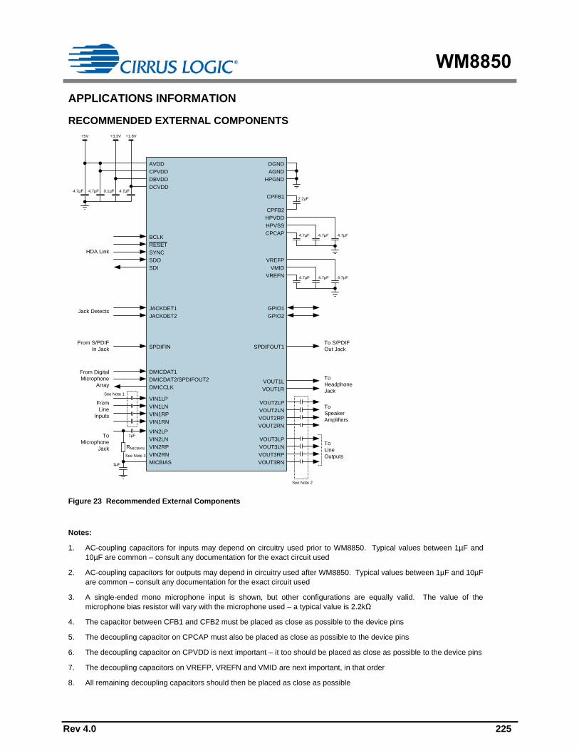
WM8850
Rev 4.0 225
APPLICATIONS INFORMATION
RECOMMENDED EXTERNAL COMPONENTS
VOUT1L
VOUT1R
VOUT2LP
VOUT2LN
VOUT2RP
VOUT2RN
VOUT3LP
VOUT3LN
VOUT3RP
VOUT3RN
To
Speaker
Amplifiers
To
Line
Outputs
To
Headphone
Jack
VIN1LP
VIN1LN
VIN1RP
VIN1RN
From
Line
Inputs
VIN2LP
VIN2LN
VIN2RP
VIN2RN
To
Microphone
Jack
MICBIAS
DMICDAT1
DMICDAT2/SPDIFOUT2
DMICCLK
From Digital
Microphone
Array
AVDD
CPVDD
DBVDD
DCVDD
+1.8V+3.3V+5V
4.7µF 4.7µF 0.1µF 4.7µF
CPCAP
CPFB1
CPFB2
HPVDD
HPVSS
1µF
2.2µF
4.7µF 4.7µF 4.7µF
VREFN
VREFP
VMID
4.7µF 4.7µF 4.7µF
DGND
AGND
HPGND
SPDIFIN SPDIFOUT1To S/PDIF
Out Jack
From S/PDIF
In Jack
JACKDET1
JACKDET2
SDO
SDI
RESET
SYNC
BCLK
HDA Link
GPIO1
GPIO2Jack Detects
RMICBIAS
See Note 2
1µF
See Note 1
See Note 3
Figure 23 Recommended External Components
Notes:
1. AC-coupling capacitors for inputs may depend on circuitry used prior to WM8850. Typical values between 1µF and
10µF are common – consult any documentation for the exact circuit used
2. AC-coupling capacitors for outputs may depend in circuitry used after WM8850. Typical values between 1µF and 10µF
are common – consult any documentation for the exact circuit used
3. A single-ended mono microphone input is shown, but other configurations are equally valid. The value of the
microphone bias resistor will vary with the microphone used – a typical value is 2.2kΩ
4. The capacitor between CFB1 and CFB2 must be placed as close as possible to the device pins
5. The decoupling capacitor on CPCAP must also be placed as close as possible to the device pins
6. The decoupling capacitor on CPVDD is next important – it too should be placed as close as possible to the device pins
7. The decoupling capacitors on VREFP, VREFN and VMID are next important, in that order
8. All remaining decoupling capacitors should then be placed as close as possible

WM8850
226 Rev 4.0
REQUIRED JACK DETECT COMPONENTS
AVDD
10kΩ
20kΩ 39kΩ10kΩ
VO
UT
1
SP
DIF
OU
T
VIN
1
JACKDET1
AVDD
10kΩ
20kΩ 39kΩ10kΩ
VIN
2
VO
UT
3
VO
UT
2
JACKDET2
Figure 24 Required Jack Detect Components
The WM8850 supports jack detect on all analogue input and output ports, as well as on the S/PDIF output. This is
implemented as per the High Definition Audio Specification Revision 1.0, section 7.4.2 and as such requires the resistor
values shown in Figure 24 above. Note that, as per the High Definition Audio Specification, it is a requirement that the
tolerance on these resistors is 1% or better.
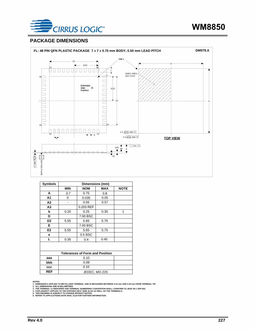
WM8850
Rev 4.0 227
PACKAGE DIMENSIONS
DM079.AFL: 48 PIN QFN PLASTIC PACKAGE 7 X 7 X 0.75 mm BODY, 0.50 mm LEAD PITCH
INDEX AREA
(D/2 X E/2)
TOP VIEW
Caaa2 X
E2
E2/2
D2
24
L
D2/2
Caaa2 X
25
36
37 48
1
12
13
D
E
e
PIN 1
A
A1
Symbols Dimensions (mm)
MIN NOM MAX NOTE
A
b
D
D2
E
E2
e
L
0.75
0.300.250.20
7.00 BSC
5.755.655.55
7.00 BSC
0.5 BSC
5.65 5.755.55
0.35 0.4 0.45
1
A1
A3
0 0.035 0.05
0.203 REF
NOTES:
1. DIMENSION b APPLIED TO METALLIZED TERMINAL AND IS MEASURED BETWEEN 0.15 mm AND 0.30 mm FROM TERMINAL TIP.
2. ALL DIMENSIONS ARE IN MILLIMETRES
3. THE TERMINAL #1 IDENTIFIER AND TERMINAL NUMBERING CONVENTION SHALL CONFORM TO JESD 95-1 SPP-002.
4. COPLANARITY APPLIES TO THE EXPOSED HEAT SINK SLUG AS WELL AS THE TERMINALS.5. THIS DRAWING IS SUBJECT TO CHANGE WITHOUT NOTICE.
6. REFER TO APPLICATIONS NOTE WAN_0118 FOR FURTHER INFORMATION.
JEDEC, MO-220
Tolerances of Form and Position
aaa
bbb
ccc
0.10
0.08
0.10
REF
EXPOSED
GND
PADDLE
6
0.7 0.8
A2 - 0.55 0.57
A2
Cccc
b
Cbb
b
(A3)
C
SE
AT
ING
PLA
NE
WM8850
228 Rev 4.0
IMPORTANT NOTICE
Contacting Cirrus Logic Support For all product questions and inquiries, contact a Cirrus Logic Sales Representative.
To find one nearest you, go to www.cirrus.com.
For the purposes of our terms and conditions of sale, "Preliminary" or "Advanced" datasheets are non-final datasheets that
include but are not limited to datasheets marked as “Target”, “Advance”, “Product Preview”, “Preliminary Technical Data”
and/or “Pre-production.” Products provided with any such datasheet are therefore subject to relevant terms and conditions
associated with "Preliminary" or "Advanced" designations. The products and services of Cirrus Logic International (UK)
Limited; Cirrus Logic, Inc.; and other companies in the Cirrus Logic group (collectively either “Cirrus Logic” or “Cirrus”) are
sold subject to Cirrus Logic’s terms and conditions of sale supplied at the time of order acknowledgment, including those
pertaining to warranty, indemnification, and limitation of liability. Software is provided pursuant to applicable license terms.
Cirrus Logic reserves the right to make changes to its products and specifications or to discontinue any product or service
without notice. Customers should therefore obtain the latest version of relevant information from Cirrus Logic to verify that
the information is current and complete. Testing and other quality control techniques are utilized to the extent Cirrus Logic
deems necessary. Specific testing of all parameters of each device is not necessarily performed. In order to minimize risks
associated with customer applications, the customer must use adequate design and operating safeguards to minimize
inherent or procedural hazards. Cirrus Logic is not liable for applications assistance or customer product design. The
customer is solely responsible for its selection and use of Cirrus Logic products. Use of Cirrus Logic products may entail a
choice between many different modes of operation, some or all of which may require action by the user, and some or all of
which may be optional. Nothing in these materials should be interpreted as instructions or suggestions to choose one mode
over another. Likewise, description of a single mode should not be interpreted as a suggestion that other modes should not
be used or that they would not be suitable for operation. Features and operations described herein are for illustrative
purposes only.
CERTAIN APPLICATIONS USING SEMICONDUCTOR PRODUCTS MAY INVOLVE POTENTIAL RISKS OF DEATH,
PERSONAL INJURY, OR SEVERE PROPERTY OR ENVIRONMENTAL DAMAGE (“CRITICAL APPLICATIONS”). CIRRUS
LOGIC PRODUCTS ARE NOT DESIGNED, AUTHORIZED OR WARRANTED FOR USE IN PRODUCTS SURGICALLY
IMPLANTED INTO THE BODY, AUTOMOTIVE SAFETY OR SECURITY DEVICES, NUCLEAR SYSTEMS, LIFE
SUPPORT PRODUCTS OR OTHER CRITICAL APPLICATIONS. INCLUSION OF CIRRUS LOGIC PRODUCTS IN SUCH
APPLICATIONS IS UNDERSTOOD TO BE FULLY AT THE CUSTOMER’S RISK AND CIRRUS LOGIC DISCLAIMS AND
MAKES NO WARRANTY, EXPRESS, STATUTORY OR IMPLIED, INCLUDING THE IMPLIED WARRANTIES OF
MERCHANTABILITY AND FITNESS FOR PARTICULAR PURPOSE, WITH REGARD TO ANY CIRRUS LOGIC PRODUCT
THAT IS USED IN SUCH A MANNER. IF THE CUSTOMER OR CUSTOMER’S CUSTOMER USES OR PERMITS THE
USE OF CIRRUS LOGIC PRODUCTS IN CRITICAL APPLICATIONS, CUSTOMER AGREES, BY SUCH USE, TO FULLY
INDEMNIFY CIRRUS LOGIC, ITS OFFICERS, DIRECTORS, EMPLOYEES, DISTRIBUTORS AND OTHER AGENTS
FROM ANY AND ALL LIABILITY, INCLUDING ATTORNEYS’ FEES AND COSTS, THAT MAY RESULT FROM OR ARISE
IN CONNECTION WITH THESE USES.
This document is the property of Cirrus Logic and by furnishing this information, Cirrus Logic grants no license, express or
implied, under any patents, mask work rights, copyrights, trademarks, trade secrets or other intellectual property rights. Any
provision or publication of any third party’s products or services does not constitute Cirrus Logic’s approval, license,
warranty or endorsement thereof. Cirrus Logic gives consent for copies to be made of the information contained herein only
for use within your organization with respect to Cirrus Logic integrated circuits or other products of Cirrus Logic, and only if
the reproduction is without alteration and is accompanied by all associated copyright, proprietary and other notices and
conditions (including this notice). This consent does not extend to other copying such as copying for general distribution,
advertising or promotional purposes, or for creating any work for resale. This document and its information is provided “AS
IS” without warranty of any kind (express or implied). All statutory warranties and conditions are excluded to the fullest
extent possible. No responsibility is assumed by Cirrus Logic for the use of information herein, including use of this
information as the basis for manufacture or sale of any items, or for infringement of patents or other rights of third parties.
Cirrus Logic, Cirrus, the Cirrus Logic logo design, and SoundClear are among the trademarks of Cirrus Logic. Other brand
and product names may be trademarks or service marks of their respective owners.
Copyright © 2010–2016 Cirrus Logic, Inc. All rights reserved.
WM8850
Rev 4.0 229
REVISION HISTORY
DATE REV DESCRIPTION OF CHANGES PAGE CHANGED BY
04/01/11 3.1 Order Info: updated to show both non tape and reel and tape and
reel parts
9 JMacD
13/04/11 3.2 AVDD and CPVDD max voltage = 5V +5% 1,11 CT
21/12/16 4.0 Beep Generator added to Block Diagram
Added Power Consumption Information
2
26
PH
CT
Related Documents