Wireless Components ASK Single Conversion Receiver TDA 5200 Version 2.7 Specification March 2000

Welcome message from author
This document is posted to help you gain knowledge. Please leave a comment to let me know what you think about it! Share it to your friends and learn new things together.
Transcript

Wireless Components
ASK Single Conversion Receiver
TDA 5200 Version 2.7
Specification March 2000

Edition 03.00Published by Infineon Technologies AG,Balanstraße 73,81541 München© Infineon Technologies AG March 2000.All Rights Reserved.Attention please!As far as patents or other rights of third parties are concerned, liability is only assumed for components, not for applications, processes and circuits im-plemented within components or assemblies.The information describes the type of component and shall not be considered as assured characteristics.Terms of delivery and rights to change design reserved.Due to technical requirements components may contain dangerous substances. For information on the types in question please contact your nearest Infineon Technologies Office.Infineon Technologies AG is an approved CECC manufacturer.PackingPlease use the recycling operators known to you. We can also help you – get in touch with your nearest sales office. By agreement we will take packing material back, if it is sorted. You must bear the costs of transport. For packing material that is returned to us unsorted or which we are not obliged to accept, we shall have to invoice you for any costs incurred.Components used in life-support devices or systems must be expressly authorized for such purpose!Critical components1 of the Infineon Technologies AG, may only be used in life-support devices or systems2 with the express written approval of the Infineon Technologies AG.1 A critical component is a component used in a life-support device or system whose failure can reasonably be expected to cause the failure of that life-
support device or system, or to affect its safety or effectiveness of that device or system.2 Life support devices or systems are intended (a) to be implanted in the human body, or (b) to support and/or maintain and sustain human life. If they
fail, it is reasonable to assume that the health of the user may be endangered.
ABM®, AOP®, ARCOFI®, ARCOFI®-BA, ARCOFI®-SP, DigiTape®, EPIC®-1, EPIC®-S, ELIC®, FALC®54, FALC®56, FALC®-E1, FALC®-LH, IDEC®, IOM®, IOM®-1, IOM®-2, IPAT®-2, ISAC®-P, ISAC®-S, ISAC®-S TE, ISAC®-P TE, ITAC®, IWE®, MUSAC®-A, OCTAT®-P, QUAT®-S, SICAT®, SICOFI®, SICOFI®-2, SICOFI®-4, SICOFI®-4µC, SLICOFI® are registered trademarks of Infineon Technologies AG.
ACE™, ASM™, ASP™, POTSWIRE™, QuadFALC™, SCOUT™ are trademarks of Infineon Technologies AG.
Revision History
Current Version: 2.7 as of 07.03.2000
Previous Version: 2.6, November 1999
Page(in previous Version)
Page(in current Version)
Subjects (major changes since last revision)

Product Info
Product InfoWireless Components
Specification, March 2000
Package
TDA 5200
Product Info
General Description The IC is a very low power consump-tion single chip ASK Single Conver-sion Receiver for the frequency bands 868-870 MHz and 433-435 MHz. The IC offers a high level of integration and needs only a few external compo-nents. The device contains a low noise amplifier (LNA), a double balanced mixer, a fully integrated VCO, a PLL synthesiser, a crystal oscillator, a lim-iter with RSSI generator, a data filter, a data comparator (slicer) and a peak detector. Additionally there is a power down feature to save battery life.
Features Low supply current (Is = 4.8mA typ. at 868MHz, Is = 4.6mA typ. at 434MHz)
Supply voltage range 5V ±10%
Power down mode with very low supply current (50nA typ)
Fully integrated VCO and PLL Synthesiser
RF input sensitivity < –107dBm
Selectable frequency ranges 868-870 MHz and 433-435 MHz
Limiter with RSSI generation, operating at 10.7MHz
Selectable reference frequency
2nd order low pass data filter with external capacitors
Data slicer with self-adjusting threshold
Application Keyless Entry Systems
Remote Control Systems
Alarm Systems
Low Bitrate CommunicationSystems
Ordering Information
Type Ordering Code Package
TDA 5200 Q67037-A1049 P-TSSOP-28-1
available on tape and reel

1 Table of Contents
1 Table of Contents . . . . . . . . . . . . . . . . . . . . . . . . . . . . . . . . . . . . . . . . . . . . . . . . . . . . . . . . . . . . i
2 Product Description . . . . . . . . . . . . . . . . . . . . . . . . . . . . . . . . . . . . . . . . . . . . . . . . . . . . . . . . . . 2-1
2.1 Overview. . . . . . . . . . . . . . . . . . . . . . . . . . . . . . . . . . . . . . . . . . . . . . . . . . . . . . . . . . . . . . . 2-2
2.2 Application . . . . . . . . . . . . . . . . . . . . . . . . . . . . . . . . . . . . . . . . . . . . . . . . . . . . . . . . . . . . . 2-2
2.3 Features . . . . . . . . . . . . . . . . . . . . . . . . . . . . . . . . . . . . . . . . . . . . . . . . . . . . . . . . . . . . . . . 2-2
2.4 Package Outlines . . . . . . . . . . . . . . . . . . . . . . . . . . . . . . . . . . . . . . . . . . . . . . . . . . . . . . . . 2-3
3 Functional Description . . . . . . . . . . . . . . . . . . . . . . . . . . . . . . . . . . . . . . . . . . . . . . . . . . . . . . . . 3-1
3.1 Pin Configuration . . . . . . . . . . . . . . . . . . . . . . . . . . . . . . . . . . . . . . . . . . . . . . . . . . . . . . . . 3-2
3.2 Pin Definition and Function. . . . . . . . . . . . . . . . . . . . . . . . . . . . . . . . . . . . . . . . . . . . . . . . . 3-3
3.3 Functional Block Diagram. . . . . . . . . . . . . . . . . . . . . . . . . . . . . . . . . . . . . . . . . . . . . . . . . . 3-9
3.4 Functional Blocks . . . . . . . . . . . . . . . . . . . . . . . . . . . . . . . . . . . . . . . . . . . . . . . . . . . . . . . . 3-10
3.4.1 Low Noise Amplifier (LNA) . . . . . . . . . . . . . . . . . . . . . . . . . . . . . . . . . . . . . . . . . . . . . . . . . 3-10
3.4.2 Mixer. . . . . . . . . . . . . . . . . . . . . . . . . . . . . . . . . . . . . . . . . . . . . . . . . . . . . . . . . . . . . . . . . . 3-10
3.4.3 PLL Synthesizer . . . . . . . . . . . . . . . . . . . . . . . . . . . . . . . . . . . . . . . . . . . . . . . . . . . . . . . . . 3-10
3.4.4 Crystal Oscillator . . . . . . . . . . . . . . . . . . . . . . . . . . . . . . . . . . . . . . . . . . . . . . . . . . . . . . . . 3-11
3.4.5 Limiter. . . . . . . . . . . . . . . . . . . . . . . . . . . . . . . . . . . . . . . . . . . . . . . . . . . . . . . . . . . . . . . . . 3-11
3.4.6 Data Filter . . . . . . . . . . . . . . . . . . . . . . . . . . . . . . . . . . . . . . . . . . . . . . . . . . . . . . . . . . . . . . 3-11
3.4.7 Data Slicer . . . . . . . . . . . . . . . . . . . . . . . . . . . . . . . . . . . . . . . . . . . . . . . . . . . . . . . . . . . . . 3-12
3.4.8 Peak Detector. . . . . . . . . . . . . . . . . . . . . . . . . . . . . . . . . . . . . . . . . . . . . . . . . . . . . . . . . . . 3-12
3.4.9 Bandgap Reference Circuitry . . . . . . . . . . . . . . . . . . . . . . . . . . . . . . . . . . . . . . . . . . . . . . . 3-12
4 Applications . . . . . . . . . . . . . . . . . . . . . . . . . . . . . . . . . . . . . . . . . . . . . . . . . . . . . . . . . . . . . . . . . 4-1
4.1 Choice of LNA Threshold Voltage and Time Constant. . . . . . . . . . . . . . . . . . . . . . . . . . . . 4-2
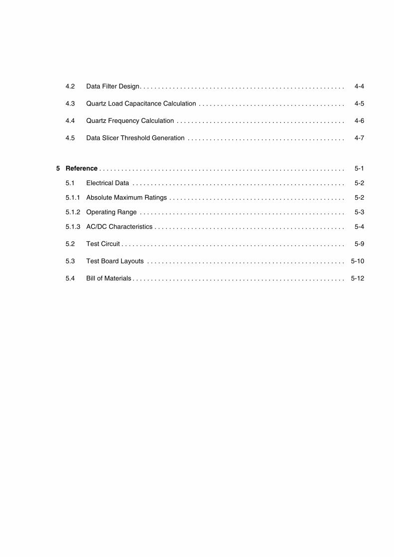
4.2 Data Filter Design. . . . . . . . . . . . . . . . . . . . . . . . . . . . . . . . . . . . . . . . . . . . . . . . . . . . . . . . 4-4
4.3 Quartz Load Capacitance Calculation . . . . . . . . . . . . . . . . . . . . . . . . . . . . . . . . . . . . . . . . 4-5
4.4 Quartz Frequency Calculation . . . . . . . . . . . . . . . . . . . . . . . . . . . . . . . . . . . . . . . . . . . . . . 4-6
4.5 Data Slicer Threshold Generation . . . . . . . . . . . . . . . . . . . . . . . . . . . . . . . . . . . . . . . . . . . 4-7
5 Reference . . . . . . . . . . . . . . . . . . . . . . . . . . . . . . . . . . . . . . . . . . . . . . . . . . . . . . . . . . . . . . . . . . . 5-1
5.1 Electrical Data . . . . . . . . . . . . . . . . . . . . . . . . . . . . . . . . . . . . . . . . . . . . . . . . . . . . . . . . . . 5-2
5.1.1 Absolute Maximum Ratings . . . . . . . . . . . . . . . . . . . . . . . . . . . . . . . . . . . . . . . . . . . . . . . . 5-2
5.1.2 Operating Range . . . . . . . . . . . . . . . . . . . . . . . . . . . . . . . . . . . . . . . . . . . . . . . . . . . . . . . . 5-3
5.1.3 AC/DC Characteristics . . . . . . . . . . . . . . . . . . . . . . . . . . . . . . . . . . . . . . . . . . . . . . . . . . . . 5-4
5.2 Test Circuit . . . . . . . . . . . . . . . . . . . . . . . . . . . . . . . . . . . . . . . . . . . . . . . . . . . . . . . . . . . . . 5-9
5.3 Test Board Layouts . . . . . . . . . . . . . . . . . . . . . . . . . . . . . . . . . . . . . . . . . . . . . . . . . . . . . . 5-10
5.4 Bill of Materials . . . . . . . . . . . . . . . . . . . . . . . . . . . . . . . . . . . . . . . . . . . . . . . . . . . . . . . . . . 5-12

2 Product Description
2.1 Overview. . . . . . . . . . . . . . . . . . . . . . . . . . . . . . . . . . . . . . . . . . . . . . . 2-22.2 Application . . . . . . . . . . . . . . . . . . . . . . . . . . . . . . . . . . . . . . . . . . . . . 2-22.3 Features . . . . . . . . . . . . . . . . . . . . . . . . . . . . . . . . . . . . . . . . . . . . . . . 2-22.4 Package Outlines . . . . . . . . . . . . . . . . . . . . . . . . . . . . . . . . . . . . . . . . 2-3
Contents of this Chapter
Product Description
TDA 5200
2.1 Overview
The IC is a very low power consumption single chip ASK Single Conversion Receiver for the frequency bands 868-870 MHz and 433-435 MHz. The IC offers a high level of integration and needs only a few external components. The device contains a low noise amplifier (LNA), a double balanced mixer, a fully integrated VCO, a PLL synthesiser, a crystal oscillator, a limiter with RSSI gen-erator, a data filter, a data comparator (slicer) and a peak detector. Additionally there is a power down feature to save battery life.
2.2 Application
Keyless Entry Systems
Remote Control Systems
Alarm Systems
Low Bitrate Communication Systems
2.3 Features
Low supply current (Is = 4.8 mA typ. at 868MHz, 4.6mA typ. at 434MHz)
Supply voltage range 5V ±10%
Power down mode with very low supply current (100nA max.)
Fully integrated VCO and PLL Synthesiser
RF input sensitivity < –107dBm
Selectable frequency ranges 868-870 MHz and 433-435 MHz
Selectable reference frequency
Limiter with RSSI generation, operating at 10.7MHz
2nd order low pass data filter with external capacitors
Data slicer with self-adjusting threshold
2 - 2Wireless Components Specification, March 2000

Product Description
TDA 5200
2.4 Package Outlines
P_TSSOP_28.EPS
Figure 2-1 P-TSSOP-28-1 package outlines
2 - 3Wireless Components Specification, March 2000

3 Functional Description
3.1 Pin Configuration . . . . . . . . . . . . . . . . . . . . . . . . . . . . . . . . . . . . . . . . 3-23.2 Pin Definition and Function. . . . . . . . . . . . . . . . . . . . . . . . . . . . . . . . . 3-33.3 Functional Block Diagram. . . . . . . . . . . . . . . . . . . . . . . . . . . . . . . . . . 3-93.4 Functional Blocks . . . . . . . . . . . . . . . . . . . . . . . . . . . . . . . . . . . . . . . 3-10
Contents of this Chapter
Functional Description
TDA 5200
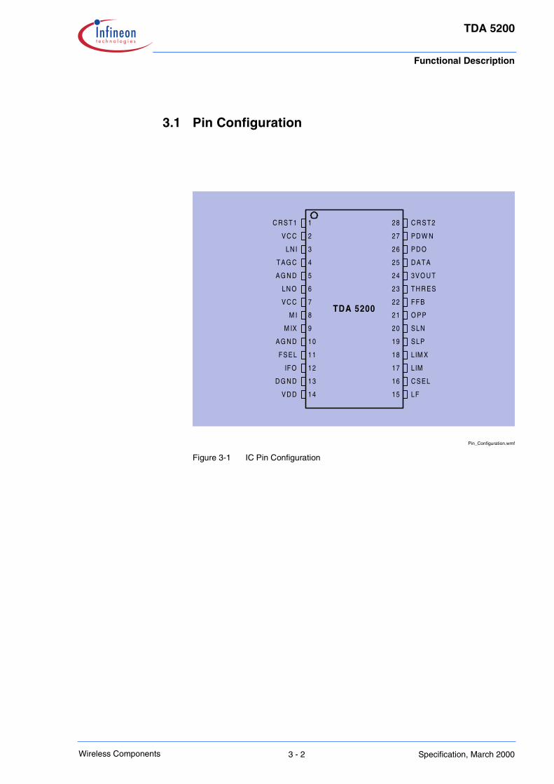
3.1 Pin Configuration
Pin_Configuration.wmf
Figure 3-1 IC Pin Configuration
C R ST 2
PD W N
PD O
D AT A
3VO U T
T H R ES
F F B
O PP
SLN
SLP
LIM X
LIM
C SEL
LF
C R ST 1
VC C
LN I
TAG C
AG N D
LN O
VC C
M I
M IX
AG N D
FSEL
IF O
D G N D
VD D
1
2
3
4
5
6
7
8
9
10
11
12
13
14
28
27
26
25
24
23
22
21
20
19
18
17
16
15
TDA 5200
3 - 2Wireless Components Specification, March 2000
Functional Description
TDA 5200
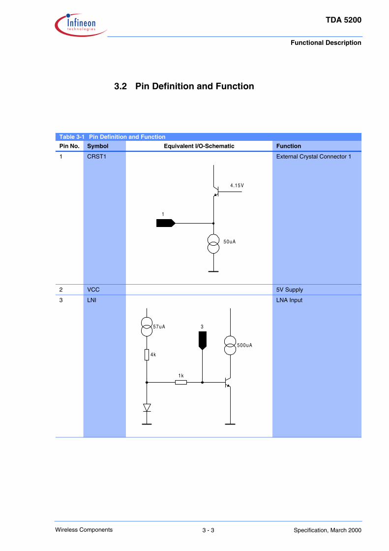
3.2 Pin Definition and Function
Table 3-1 Pin Definition and Function
Pin No. Symbol Equivalent I/O-Schematic Function
1 CRST1 External Crystal Connector 1
2 VCC 5V Supply
3 LNI LNA Input
4.15V
50uA
1
57uA
4k
1k
3
500uA
3 - 3Wireless Components Specification, March 2000

Functional Description
TDA 5200
4 TAGC AGC Time Constant Control
5 AGND Analogue Ground Return
6 LNO LNA Output
7 VCC 5V Supply
8
9
MI
MIX
Mixer Input
Complementary Mixer Input
10 AGND Analogue Ground Return
1k
3uA
1 .4uA
1 .7V
4.3V
4
6
1k
5V
8
1.7V
9
400uA
2k 2k
3 - 4Wireless Components Specification, March 2000
Functional Description
TDA 5200
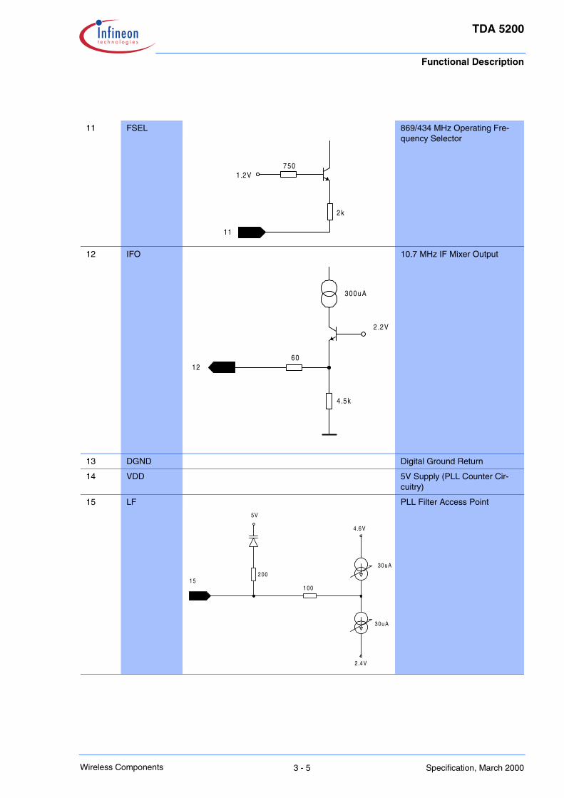
11 FSEL 869/434 MHz Operating Fre-quency Selector
12 IFO 10.7 MHz IF Mixer Output
13 DGND Digital Ground Return
14 VDD 5V Supply (PLL Counter Cir-cuitry)
15 LF PLL Filter Access Point
750
2k
11
1.2V
2.2V
4.5k
6012
300uA
15200
30uA
30uA
4.6V
2.4V
5V
100
3 - 5Wireless Components Specification, March 2000
Functional Description
TDA 5200
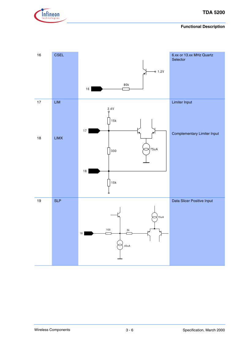
16 CSEL 6.xx or 13.xx MHz Quartz Selector
17
18
LIM
LIMX
Limiter Input
Complementary Limiter Input
19 SLP Data Slicer Positive Input
1.2V
80k16
330
15k
15k
18
17
2.4V
75uA
19
40uA
15uA
3k100
3 - 6Wireless Components Specification, March 2000
Functional Description
TDA 5200
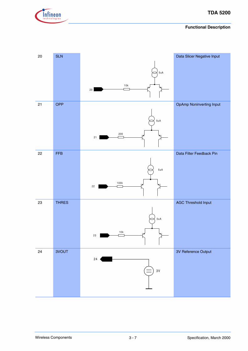
20 SLN Data Slicer Negative Input
21 OPP OpAmp Noninverting Input
22 FFB Data Filter Feedback Pin
23 THRES AGC Threshold Input
24 3VOUT 3V Reference Output
5uA
20
10k
21200
5uA
100k
5uA
22
10k
5uA
23
3V
24
3 - 7Wireless Components Specification, March 2000
Functional Description
TDA 5200
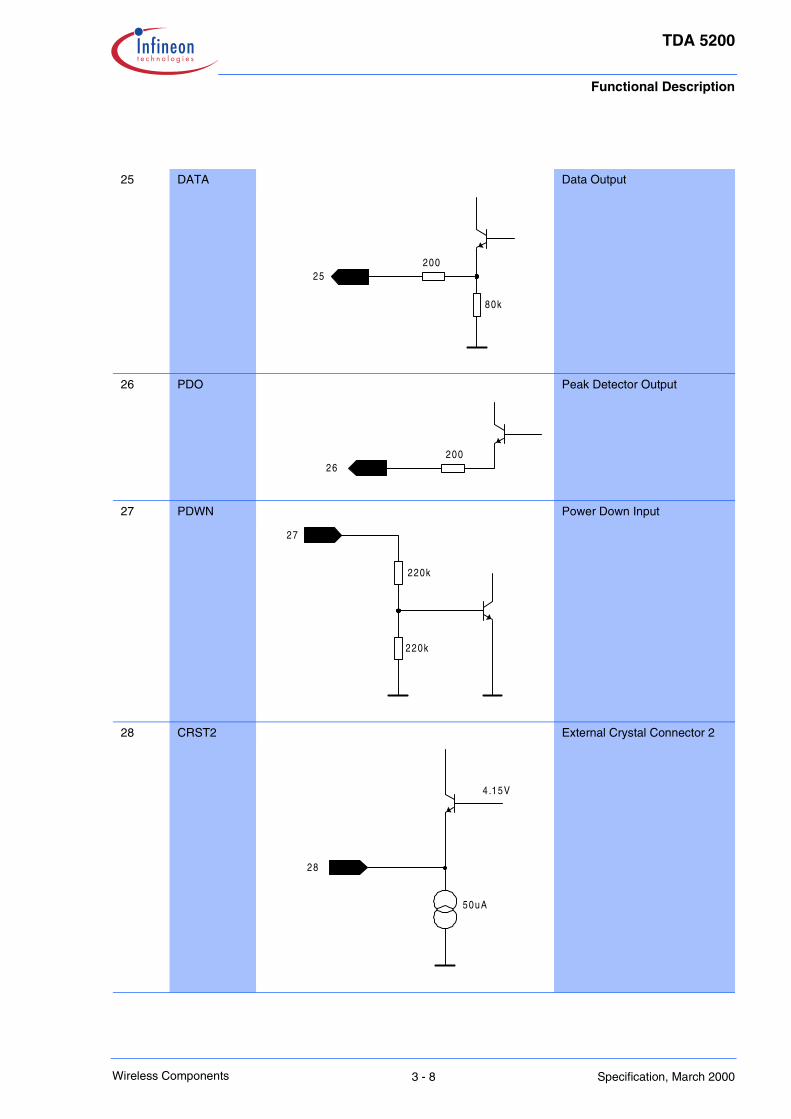
25 DATA Data Output
26 PDO Peak Detector Output
27 PDWN Power Down Input
28 CRST2 External Crystal Connector 2
25200
80k
26200
27
220k
220k
4 .15V
50uA
28
3 - 8Wireless Components Specification, March 2000

Functional Description
TDA 5200
3.3 Functional Block Diagram
Function_5200.wmf
Figure 3-2 Main Block Diagram
IFFilter
VDD
VCC
LNO MI MIX IFO LIM LIMX FFB OPP SLP SLN
DATA
PDO
SLICERRSSI
THRES
LNARF
TAGC
DGND
VCC AGND FSEL CSEL PDWN
Crystal
LoopFilter
BandgapReference
UREF
TDA 5200 AGCReference
3VOUT
3
4
14
13
2/7 5/10 11 15LF
16 1 28 27
24
23
26
25
20192122181712986
CrystalOSC
ΦDET: 128/64VCO: 1/2
3 - 9Wireless Components Specification, March 2000
Functional Description
TDA 5200
3.4 Functional Blocks
3.4.1 Low Noise Amplifier (LNA)
The LNA is an on-chip cascode amplifier with a voltage gain of 15 to 20dB. The gain figure is determined by the external matching networks situated ahead of LNA and between the LNA output LNO (Pin 6) and the Mixer Inputs MI and MIX (Pins 8 and 9). The noise figure of the LNA is approximately 3.2dB, the current consumption is 500µA. The gain can be reduced by approximately 18dB. The switching point of this AGC action can be determined externally by applying a threshold voltage at the THRES pin (Pin 23). This voltage is compared internally with the received signal (RSSI) level generated by the limiter circuitry. In case that the RSSI level is higher than the threshold voltage the LNA gain is reduced and vice versa. The threshold voltage can be generated by attaching a voltage divider between the 3VOUT pin (Pin 24) which provides a temperature stable 3V output generated from the internal bandgap voltage and the THRES pin as described in Section 4.1. The time constant of the AGC action can be deter-mined by connecting a capacitor to the TAGC pin (Pin 4) and should be chosen along with the appropriate threshold voltage according to the intended operat-ing case and interference scenario to be expected during operation. The opti-mum choice of AGC time constant and the threshold voltage is described in Section 4.1.
3.4.2 Mixer
The Double Balanced Mixer downconverts the input frequency (RF) in the range of 433-435MHz/868-870MHz to the intermediate frequency (IF) at 10.7MHz with a voltage gain of approximately 21dB. A low pass filter with a cor-ner frequency of 20MHz is built on chip in order to suppress RF signals to appear at the IF output ( IFO pin). The IF output is internally consisting of an emitter follower that has a source impedance of approximately 330 Ω=to facili-tate interfacing the pin directly to a standard 10.7MHz ceramic filter without additional matching circuitry.
3.4.3 PLL Synthesizer
The Phase Locked Loop synthesiser consists of a VCO, an asynchronous divider chain, a phase detector with charge pump and a loop filter and is fully implemented on-chip. The VCO is including spiral inductors and varactor diodes. It’s nominal centre frequency is 852MHz. No additional components are necessary. The oscillator signal is fed both to the synthesiser divider chain and to the downconverting mixer. In case of operation in the 433 - 435 MHz range, the signal is divided by two before it is fed to the mixer. This is controlled by the selection pin FSEL (Pin 11) as described in the following table. The overall divi-
3 - 10Wireless Components Specification, March 2000
Functional Description
TDA 5200
sion ratio of the divider chain can be selected to be either 128 or 64, depending on the frequency of the reference oscillator quartz (see below). The loop filter is also realised fully on-chip.
3.4.4 Crystal Oscillator
The on-chip crystal oscillator circuitry allows for utilisation of quartzes both in the 6 and 13MHz range as the overall division ratio of the PLL can be switched between 64 and 128 via the CSEL (Pin 16 ) pin according to the following table.
The calculation of the value of the necessary quartz load capacitance is shown in Section 4.3, the quartz frequency calculation is expained in Section 4.4.
3.4.5 Limiter
The Limiter is an AC coupled multistage amplifier with a cumulative gain of approximately 80dB that has a bandpass-characteristic centred around 10.7MHz. It has an input impedance of 330 Ω=to allow for easy interfacing to a 10.7MHz ceramic IF filter. The limiter circuit acts as a Receive Signal Strength Indicator (RSSI) generator which produces a DC voltage that is directly propor-tional to the input signal level as can be seen in Figure 4-2. This signal is used to demodulate the ASK receive signal in the subsequent baseband circuitry and to turn down the LNA gain by approximately 17dB in case the input signal strength is too strong as described in Section 3.4.1 and Section 4.1.
3.4.6 Data Filter
The data filter comprises an OP-Amp with a bandwidth of 100kHz used as a voltage follower and two 100kΩ=on-chip resistors. Along with two external capacitors a 2nd order Sallen-Key low pass filter is formed. The selection of the capacitor values is described in Section 4.2.
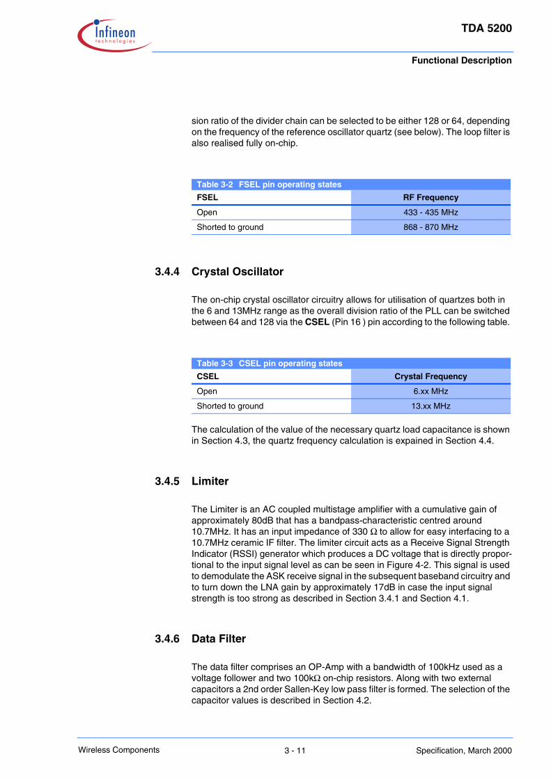
Table 3-2 FSEL pin operating states
FSEL RF Frequency
Open 433 - 435 MHz
Shorted to ground 868 - 870 MHz
Table 3-3 CSEL pin operating states
CSEL Crystal Frequency
Open 6.xx MHz
Shorted to ground 13.xx MHz
3 - 11Wireless Components Specification, March 2000

Functional Description
TDA 5200
3.4.7 Data Slicer
The data slicer is a fast comparator with a bandwidth of 100 kHz. This allows for a maximum receive data rate of approximately 120kBaud. The maximum achievable data rate also depends on the IF Filter bandwidth and the local oscil-lator tolerance values. Both inputs are accessible. The output delivers a digital data signal (CMOS-like levels) for the detector. The self-adjusting threshold on pin 20 its generated by RC-term or peak detector depending on the baseband coding scheme. The data slicer threshold generation alternatives are described in more detail in Section 4.5.
3.4.8 Peak Detector
The peak detector generates a DC voltage which is proportional to the peak value of the receive data signal. An external RC network is necessary. The out-put can be used as an indicator for the signal strength and also as a reference for the data slicer. The maximum output current is 500µA.
3.4.9 Bandgap Reference Circuitry
A Bandgap Reference Circuit provides a temperature stable reference voltage for the device. A power down mode is available to switch off all subcircuits which is controlled by the PWDN pin (Pin 27) as shown in the following table. The sup-ply current drawn in this case is typically 50nA. .
Table 3-4 PDWN pin operating states
PDWN Operating State
Open or tied to ground Powerdown Mode
Tied to Vs Receiver On
3 - 12Wireless Components Specification, March 2000
4 Applications
4.1 Choice of LNA Threshold Voltage and Time Constant . . . . . . . . . . . . 4-24.2 Data Filter Design . . . . . . . . . . . . . . . . . . . . . . . . . . . . . . . . . . . . . . . . 4-44.3 Quartz Load Capacitance Calculation . . . . . . . . . . . . . . . . . . . . . . . . 4-54.4 Quartz Frequency Calculation . . . . . . . . . . . . . . . . . . . . . . . . . . . . . . 4-64.5 Data Slicer Threshold Generation . . . . . . . . . . . . . . . . . . . . . . . . . . . 4-7
Contents of this Chapter
Applications
TDA 5200
4.1 Choice of LNA Threshold Voltage and Time Constant
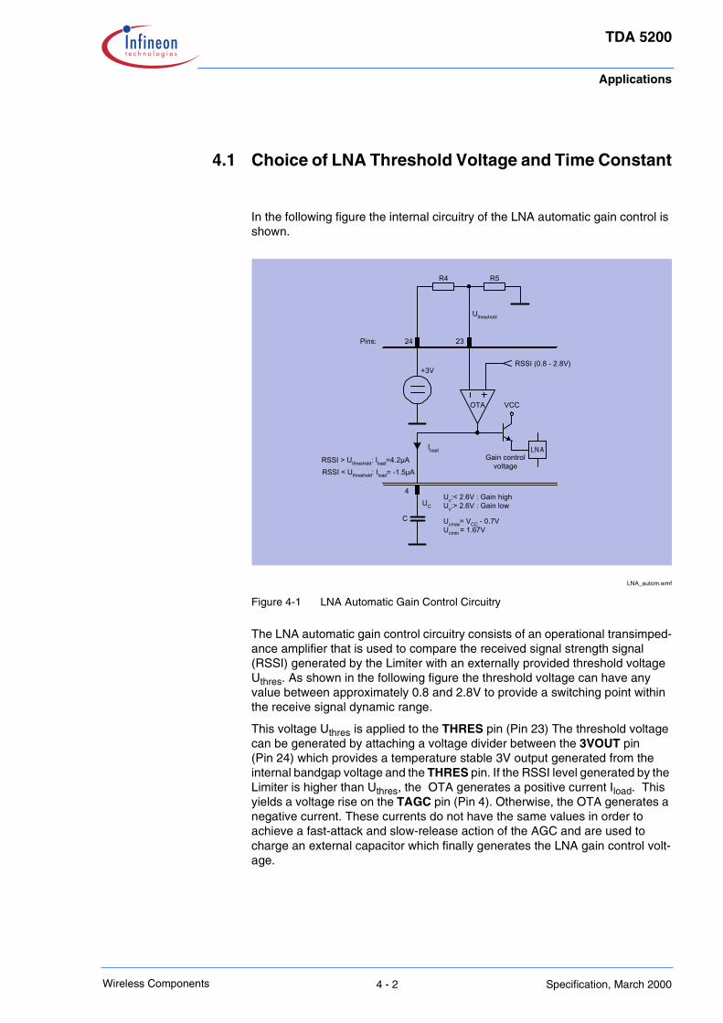
In the following figure the internal circuitry of the LNA automatic gain control is shown.
LNA_autom.wmf
Figure 4-1 LNA Automatic Gain Control Circuitry
The LNA automatic gain control circuitry consists of an operational transimped-ance amplifier that is used to compare the received signal strength signal (RSSI) generated by the Limiter with an externally provided threshold voltage Uthres. As shown in the following figure the threshold voltage can have any value between approximately 0.8 and 2.8V to provide a switching point within the receive signal dynamic range.
This voltage Uthres is applied to the THRES pin (Pin 23) The threshold voltage can be generated by attaching a voltage divider between the 3VOUT pin (Pin 24) which provides a temperature stable 3V output generated from the internal bandgap voltage and the THRES pin. If the RSSI level generated by the Limiter is higher than Uthres, the OTA generates a positive current Iload. This yields a voltage rise on the TAGC pin (Pin 4). Otherwise, the OTA generates a negative current. These currents do not have the same values in order to achieve a fast-attack and slow-release action of the AGC and are used to charge an external capacitor which finally generates the LNA gain control volt-age.
Pins: 24 23
4
LN A
R4 R5
Uthreshold
RSSI (0.8 - 2.8V)
VCC
Gain controlvoltage
OTA
+3V
Iload
RSSI > Uthreshold: Iload=4.2µARSSI < Uthreshold: Iload= -1.5µA
UC
C
Uc:< 2.6V : Gain highUc:> 2.6V : Gain low
Ucmax= VCC - 0.7VUcmin = 1.67V
4 - 2Wireless Components Specification, March 2000
Applications
TDA 5200
RSSI-AGC.wmf
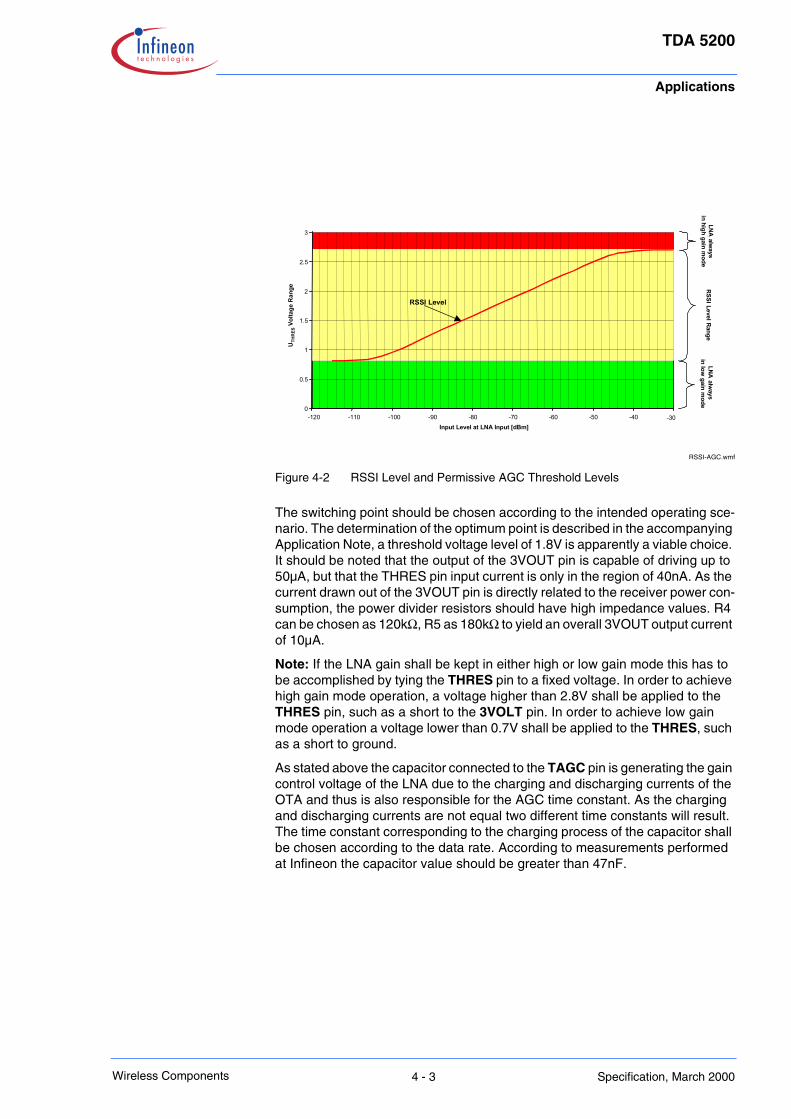
Figure 4-2 RSSI Level and Permissive AGC Threshold Levels
The switching point should be chosen according to the intended operating sce-nario. The determination of the optimum point is described in the accompanying Application Note, a threshold voltage level of 1.8V is apparently a viable choice. It should be noted that the output of the 3VOUT pin is capable of driving up to 50µA, but that the THRES pin input current is only in the region of 40nA. As the current drawn out of the 3VOUT pin is directly related to the receiver power con-sumption, the power divider resistors should have high impedance values. R4 can be chosen as 120kΩ, R5 as 180kΩ to yield an overall 3VOUT output current of 10µA.
Note: If the LNA gain shall be kept in either high or low gain mode this has to be accomplished by tying the THRES pin to a fixed voltage. In order to achieve high gain mode operation, a voltage higher than 2.8V shall be applied to the THRES pin, such as a short to the 3VOLT pin. In order to achieve low gain mode operation a voltage lower than 0.7V shall be applied to the THRES, such as a short to ground.
As stated above the capacitor connected to the TAGC pin is generating the gain control voltage of the LNA due to the charging and discharging currents of the OTA and thus is also responsible for the AGC time constant. As the charging and discharging currents are not equal two different time constants will result. The time constant corresponding to the charging process of the capacitor shall be chosen according to the data rate. According to measurements performed at Infineon the capacitor value should be greater than 47nF.
LNA always
in high gain mode
0
0.5
1
1.5
2
2.5
3
-120 -110 -100 -90 -80 -70 -60 -50 -40 -30Input Level at LNA Input [dBm]
UTH
RES
Vol
tage
Ran
ge RSSI Level RangeLNA alw
aysin low
gain mode
RSSI Level
4 - 3Wireless Components Specification, March 2000
Applications
TDA 5200
4.2 Data Filter Design
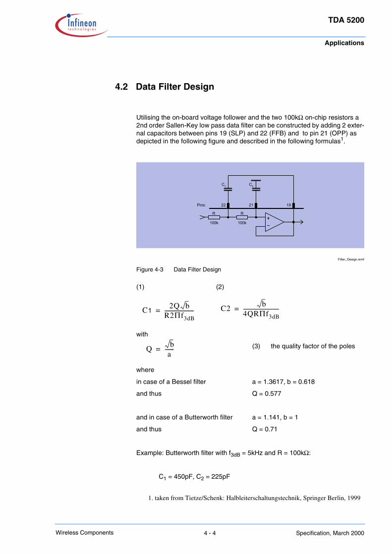
Utilising the on-board voltage follower and the two 100kΩ on-chip resistors a 2nd order Sallen-Key low pass data filter can be constructed by adding 2 exter-nal capacitors between pins 19 (SLP) and 22 (FFB) and to pin 21 (OPP) as depicted in the following figure and described in the following formulas1.
Filter_Design.wmf
Figure 4-3 Data Filter Design
(1) (2)
with
(3) the quality factor of the poles
where
in case of a Bessel filter a = 1.3617, b = 0.618
and thus Q = 0.577
and in case of a Butterworth filter a = 1.141, b = 1
and thus Q = 0.71
Example: Butterworth filter with f3dB = 5kHz and R = 100kΩ:
C1 = 450pF, C2 = 225pF
1. taken from Tietze/Schenk: Halbleiterschaltungstechnik, Springer Berlin, 1999
Pins: 22 21 19
R R
100k 100k
C1 C2
C1 2Q bR2Πf3dB----------------------= C2
b4QRΠf3dB---------------------------=
Qb
a-------=
4 - 4Wireless Components Specification, March 2000
Applications
TDA 5200
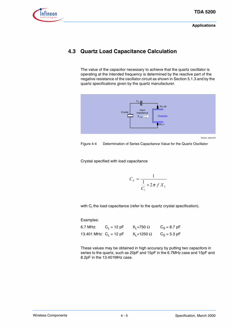
4.3 Quartz Load Capacitance Calculation
The value of the capacitor necessary to achieve that the quartz oscillator is operating at the intended frequency is determined by the reactive part of the negative resistance of the oscillator circuit as shown in Section 5.1.3 and by the quartz specifications given by the quartz manufacturer.
Quartz_load.wmf
Figure 4-4 Determination of Series Capacitance Value for the Quartz Oscillator
Crystal specified with load capacitance
with Cl the load capacitance (refer to the quartz crystal specification).
Examples:
6.7 MHz: CL = 12 pF XL=750 Ω CS = 8.7 pF
13.401 MHz: CL = 12 pF XL=1250 Ω CS = 5.3 pF
These values may be obtained in high accuracy by putting two capacitors in series to the quartz, such as 20pF and 15pF in the 6.7MHz case and 15pF and 8.2pF in the 13.401MHz case.
CS
CrystalInput
impedanceZ1-28 TDA5200
Pin 28
Pin 1
Ll
S
XfC
Cπ211
+=
4 - 5Wireless Components Specification, March 2000

Applications
TDA 5200
4.4 Quartz Frequency Calculation
The quartz frequency is calculated by using the following formula:
ƒQU = (ƒRF ± 10.7) / r (1),
with ƒRF .... receive frequency
ƒLO .... local oscillator (PLL) frequency (ƒRF ± 10.7)
ƒQU .... quartz oscillator frequency
r .... ratio of local oscillator (PLL) frequency and quartz
frequency as shown in the subsequent table.
Subtraction of 10.7 occurs in case the receive frequency is higher than the intended local oscillator frequency, addition in case the receive frequency lies below the local oscillator frequency.
Examples:
Table 4-1 PLL Division Ratio Dependence on States of FSEL and CSEL
FSEL CSEL Ratio r = (fLO/fQU)
open open 64
open GND 32
GND open 128
GND GND 64
( ) MHzMHzMHzf 40156.1364/7.104.868QU =−=
( ) MHzMHzMHzf 7008.6128/7.104.868QU =−=
( ) MHzMHzMHzf 23437.1332/7.102.434QU =−=
4 - 6Wireless Components Specification, March 2000
Applications
TDA 5200
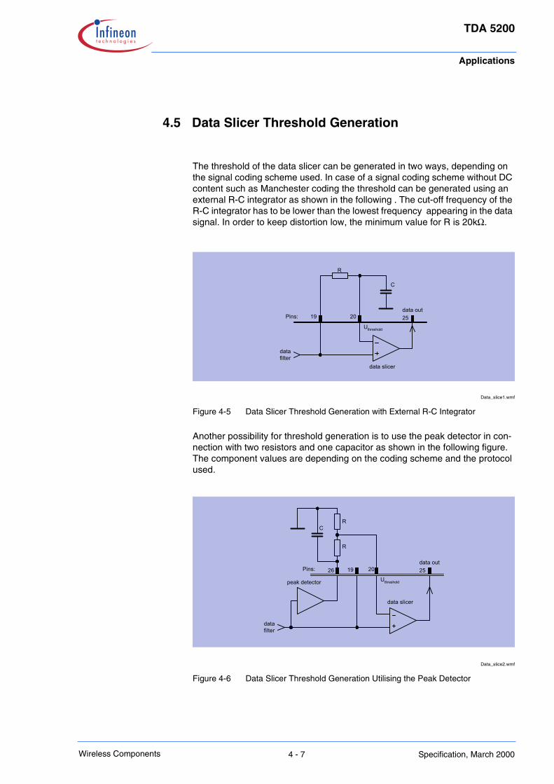
4.5 Data Slicer Threshold Generation
The threshold of the data slicer can be generated in two ways, depending on the signal coding scheme used. In case of a signal coding scheme without DC content such as Manchester coding the threshold can be generated using an external R-C integrator as shown in the following . The cut-off frequency of the R-C integrator has to be lower than the lowest frequency appearing in the data signal. In order to keep distortion low, the minimum value for R is 20kΩ.
Data_slice1.wmf
Figure 4-5 Data Slicer Threshold Generation with External R-C Integrator
Another possibility for threshold generation is to use the peak detector in con-nection with two resistors and one capacitor as shown in the following figure. The component values are depending on the coding scheme and the protocol used.
Data_slice2.wmf
Figure 4-6 Data Slicer Threshold Generation Utilising the Peak Detector
Pins: 2019
R
C
25data out
Uthreshold
data slicer
datafilter
Pins: 2019 25data out
Uthreshold
data slicer
datafilter
26
peak detector
CR
R
4 - 7Wireless Components Specification, March 2000

5 Reference
5.1 Electrical Data. . . . . . . . . . . . . . . . . . . . . . . . . . . . . . . . . . . . . . . . . . . 5-25.2 Test Circuit . . . . . . . . . . . . . . . . . . . . . . . . . . . . . . . . . . . . . . . . . . . . . 5-95.3 Test Board Layouts. . . . . . . . . . . . . . . . . . . . . . . . . . . . . . . . . . . . . . 5-105.4 Bill of Materials . . . . . . . . . . . . . . . . . . . . . . . . . . . . . . . . . . . . . . . . . 5-12
Contents of this Chapter

Reference
TDA 5200
5.1 Electrical Data
5.1.1 Absolute Maximum Ratings
WARNING
The maximum ratings may not be exceeded under any circumstances, not even momentarily and individually, as permanent damage to the IC will result.
Table 5-1 Absolute Maximum Ratings, Ambient temperature TAMB=-40°C ... + 85°C
# Parameter Symbol Limit Values Unit Remarks
min max
1 Supply Voltage Vs -0.3 5.5 V
2 Junction Temperature Tj -40 +150 °C
3 Storage Temperature Ts -40 +125 °C
4 Thermal Resistance RthJA 114 K/W
5 ESD integrity, all pins VESD -1 +1 kV HBM according to
MIL STD 883D,
method 3015.7
5 - 2Wireless Components Specification, March 2000
Reference
TDA 5200
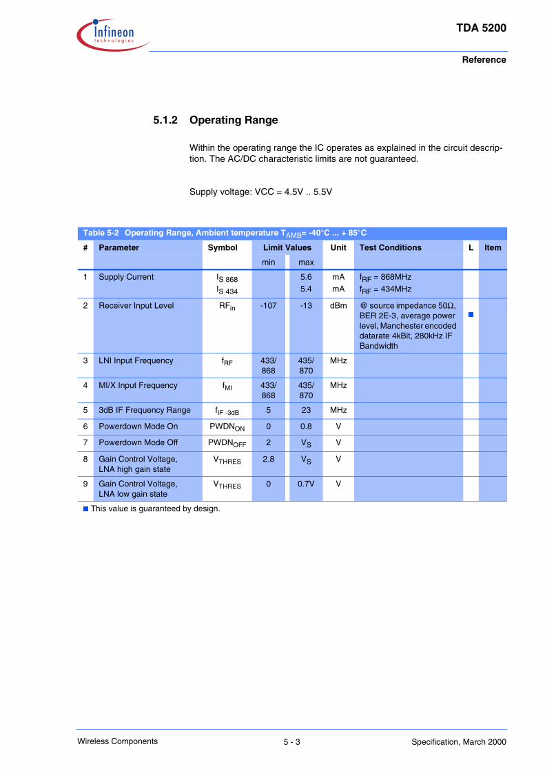
5.1.2 Operating Range
Within the operating range the IC operates as explained in the circuit descrip-tion. The AC/DC characteristic limits are not guaranteed.
Supply voltage: VCC = 4.5V .. 5.5V
Table 5-2 Operating Range, Ambient temperature TAMB= -40°C ... + 85°C
# Parameter Symbol Limit Values Unit Test Conditions L Item
min max
1 Supply Current IS 868IS 434
5.6
5.4
mA
mA
fRF = 868MHz
fRF = 434MHz
2 Receiver Input Level RFin -107 -13 dBm @ source impedance 50Ω, BER 2E-3, average power level, Manchester encoded datarate 4kBit, 280kHz IF Bandwidth
3 LNI Input Frequency fRF 433/868
435/870
MHz
4 MI/X Input Frequency fMI 433/868
435/870
MHz
5 3dB IF Frequency Range fIF -3dB 5 23 MHz
6 Powerdown Mode On PWDNON 0 0.8 V
7 Powerdown Mode Off PWDNOFF 2 VS V
8 Gain Control Voltage,LNA high gain state
VTHRES 2.8 VS V
9 Gain Control Voltage,LNA low gain state
VTHRES 0 0.7V V
This value is guaranteed by design.
5 - 3Wireless Components Specification, March 2000

Reference
TDA 5200
5.1.3 AC/DC Characteristics
AC/DC characteristics involve the spread of values guaranteed within the spec-ified voltage and ambient temperature range. Typical characteristics are the median of the production. The device performance parameters marked with were measured on an Infineon evaluation board as desdribed in Section 5.2..
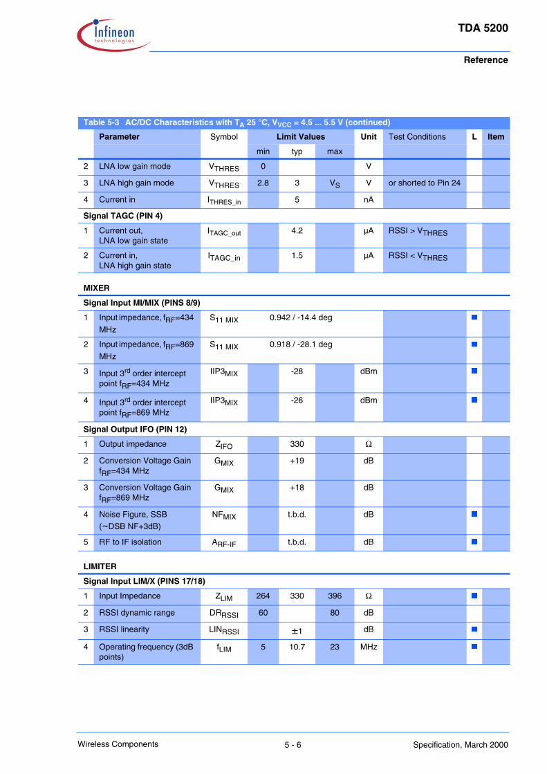
Table 5-3 AC/DC Characteristics with TA 25 °C, VVCC = 4.5 ... 5.5 V
# Parameter Symbol Limit Values Unit Test Conditions L Item
min typ max
Supply
Supply Current
1 Supply current,standby mode
IS PDWN 50 70 nA Pin 27 (PDWN) open or tied to 0 V
2 Supply current, device operating at 868MHz
IS 868 4.8 5.2 mA Pin 11 (FSEL) tied to GND
3 Supply current, device operating at 434 MHz
IS 434 4.6 5 mA Pin 11 (FSEL) open
LNA
Signal Input LNI (PIN 3), VTHRES > 2.8V, high gain mode
1 Average Power Level at BER = 2E-3(Sensitivity)
RFin -110 dBm Manchester encoded datarate 4kBit, 280kHz IF Bandwidth
2 Input impedance, fRF=434
MHz
S11 LNA 0.873 / -34.7 deg
3 Input impedance, fRF=869
MHz
S11 LNA 0.738 / -73.5 deg
4 Input level @ 1dB com-pression
P1dBLNA -15 dBm
5 Input 3rd order intercept point fRF=434 MHz
IIP3LNA -10 dBm matched input
6 Input 3rd order intercept point fRF=869 MHz
IIP3LNA -14 dBm matched input
7 LO signal feedthrough at antenna port
LOLNI -73 dBm
Signal Output LNO (PIN 6), VTHRES > 2.8V, high gain mode
1 Gain fRF=434 MHz S21 LNA 1.509 / 138.2 deg
2 Gain fRF=869 MHz S21 LNA 1.419 / 101.7 deg
3 Output impedance, fRF=434 MHz
S22 LNA 0.886 / -12.9 deg
5 - 4Wireless Components Specification, March 2000
Reference
TDA 5200
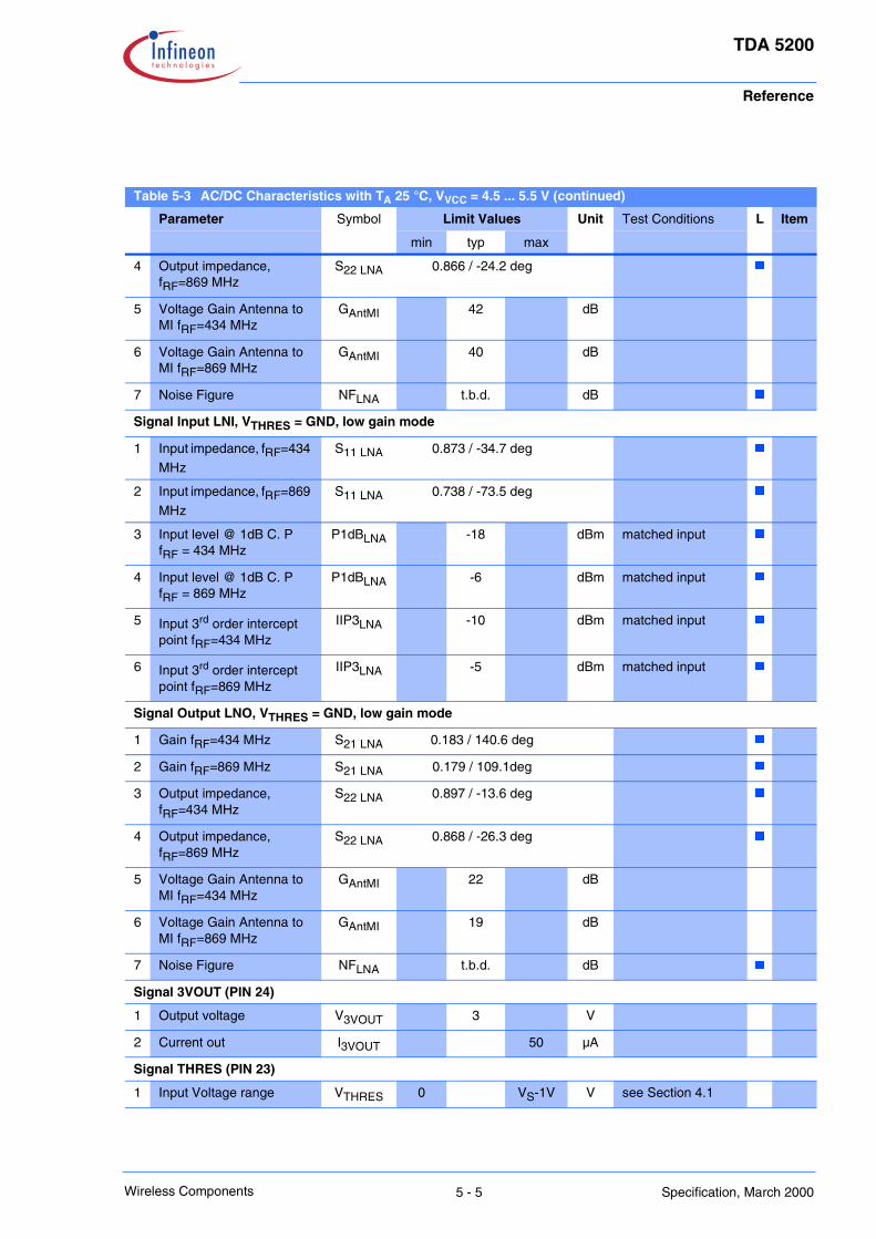
Table 5-3 AC/DC Characteristics with TA 25 °C, VVCC = 4.5 ... 5.5 V (continued)
Parameter Symbol Limit Values Unit Test Conditions L Item
min typ max
4 Output impedance, fRF=869 MHz
S22 LNA 0.866 / -24.2 deg
5 Voltage Gain Antenna to MI fRF=434 MHz
GAntMI 42 dB
6 Voltage Gain Antenna to MI fRF=869 MHz
GAntMI 40 dB
7 Noise Figure NFLNA t.b.d. dB
Signal Input LNI, VTHRES = GND, low gain mode
1 Input impedance, fRF=434
MHz
S11 LNA 0.873 / -34.7 deg
2 Input impedance, fRF=869
MHz
S11 LNA 0.738 / -73.5 deg
3 Input level @ 1dB C. PfRF = 434 MHz
P1dBLNA -18 dBm matched input
4 Input level @ 1dB C. PfRF = 869 MHz
P1dBLNA -6 dBm matched input
5 Input 3rd order intercept point fRF=434 MHz
IIP3LNA -10 dBm matched input
6 Input 3rd order intercept point fRF=869 MHz
IIP3LNA -5 dBm matched input
Signal Output LNO, VTHRES = GND, low gain mode
1 Gain fRF=434 MHz S21 LNA 0.183 / 140.6 deg
2 Gain fRF=869 MHz S21 LNA 0.179 / 109.1deg
3 Output impedance, fRF=434 MHz
S22 LNA 0.897 / -13.6 deg
4 Output impedance, fRF=869 MHz
S22 LNA 0.868 / -26.3 deg
5 Voltage Gain Antenna to MI fRF=434 MHz
GAntMI 22 dB
6 Voltage Gain Antenna to MI fRF=869 MHz
GAntMI 19 dB
7 Noise Figure NFLNA t.b.d. dB
Signal 3VOUT (PIN 24)
1 Output voltage V3VOUT 3 V
2 Current out I3VOUT 50 µA
Signal THRES (PIN 23)
1 Input Voltage range VTHRES 0 VS-1V V see Section 4.1
5 - 5Wireless Components Specification, March 2000
Reference
TDA 5200
Table 5-3 AC/DC Characteristics with TA 25 °C, VVCC = 4.5 ... 5.5 V (continued)
Parameter Symbol Limit Values Unit Test Conditions L Item
min typ max
2 LNA low gain mode VTHRES 0 V
3 LNA high gain mode VTHRES 2.8 3 VS V or shorted to Pin 24
4 Current in ITHRES_in 5 nA
Signal TAGC (PIN 4)
1 Current out,LNA low gain state
ITAGC_out 4.2 µA RSSI > VTHRES
2 Current in, LNA high gain state
ITAGC_in 1.5 µA RSSI < VTHRES
MIXER
Signal Input MI/MIX (PINS 8/9)
1 Input impedance, fRF=434
MHz
S11 MIX 0.942 / -14.4 deg
2 Input impedance, fRF=869
MHz
S11 MIX 0.918 / -28.1 deg
3 Input 3rd order intercept point fRF=434 MHz
IIP3MIX -28 dBm
4 Input 3rd order intercept point fRF=869 MHz
IIP3MIX -26 dBm
Signal Output IFO (PIN 12)
1 Output impedance ZIFO 330 Ω
2 Conversion Voltage Gain fRF=434 MHz
GMIX +19 dB
3 Conversion Voltage Gain fRF=869 MHz
GMIX +18 dB
4 Noise Figure, SSB (~DSB NF+3dB)
NFMIX t.b.d. dB
5 RF to IF isolation ARF-IF t.b.d. dB
LIMITER
Signal Input LIM/X (PINS 17/18)
1 Input Impedance ZLIM 264 330 396 Ω
2 RSSI dynamic range DRRSSI 60 80 dB
3 RSSI linearity LINRSSI ±1 dB
4 Operating frequency (3dB points)
fLIM 5 10.7 23 MHz
5 - 6Wireless Components Specification, March 2000

Reference
TDA 5200
Table 5-3 AC/DC Characteristics with TA 25 °C, VVCC = 4.5 ... 5.5 V (continued)
Parameter Symbol Limit Values Unit Test Conditions L Item
min typ max
DATA FILTER
1 Useable bandwidth BWBB FILT
100 kHz
2 RSSI Level at Data Filter Output SLP
RSSIlow 0.9 V LNA in high gain RFIN=-103dBm
3 RSSI Level at Data Filter Output SLP
RSSIhigh 2.8 V LNA in high gain.RFIN=-30dBm
SLICER
Signal Output DATA (PIN 25)
1 Useable bandwith BWBB SLIC
100 kHz
2 Capacitive loading of out-put
Cmax SLIC
20 pF
3 LOW output voltage VSLIC_L 0 V
4 HIGH output voltage VSLIC_H VS-1V V
5 Output current ISLIC_out 200 µA
PEAK DETECTOR
Signal Output PDO (PIN 26)
1 LOW output voltage VSLIC_L 0 V
2 HIGH output voltage VSLIC_H VS-1 V
3 Load current Iload 500 µA
4 Leakage current Ileakage 700 nA
CRYSTAL OSCILLATOR
Signals CRSTL1, CRISTL 2, (PINS 1/28)
1 Operating frequency fCRSTL 6 14 MHz fundamental mode, series resonance
2 Input Impedance
@ ~6MHz
Z1-28 -900+j750
Ω
3 Input Impedance
@ ~13MHz
Z1-28 -450+j1250
Ω
4 Serial Capacity
@ ~6MHz
CS 6=C1 8.7 pF
5 Serial Capacity
@ ~13MHz
CS13=C1 5.3 pF
5 - 7Wireless Components Specification, March 2000
Reference
TDA 5200
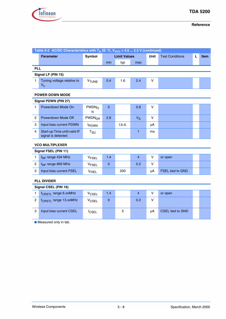
Table 5-3 AC/DC Characteristics with TA 25 °C, VVCC = 4.5 ... 5.5 V (continued)
Parameter Symbol Limit Values Unit Test Conditions L Item
min typ max
PLL
Signal LF (PIN 15)
1 Tuning voltage relative to Vs
VTUNE 0.4 1.6 2.4 V
POWER DOWN MODE
Signal PDWN (PIN 27)
1 Powerdown Mode On PWDNON
0 0.8 V
2 Powerdown Mode Off PWDNOff 2.8 VS V
3 Input bias current PDWN IPDWN t.b.d. µA
4 Start-up Time until valid IF signal is detected
TSU 1 ms
VCO MULTIPLEXER
Signal FSEL (PIN 11)
1 fRF range 434 MHz VFSEL 1.4 4 V or open
2 fRF range 869 MHz VFSEL 0 0.2 V
3 Input bias current FSEL IFSEL 200 µA FSEL tied to GND
PLL DIVIDER
Signal CSEL (PIN 16)
1 fCRSTL range 6.xxMHz VCSEL 1.4 4 V or open
2 fCRSTL range 13.xxMHz VCSEL 0 0.2 V
3 Input bias current CSEL ICSEL 5 µA CSEL tied to GND
Measured only in lab.
5 - 8Wireless Components Specification, March 2000
Reference
TDA 5200
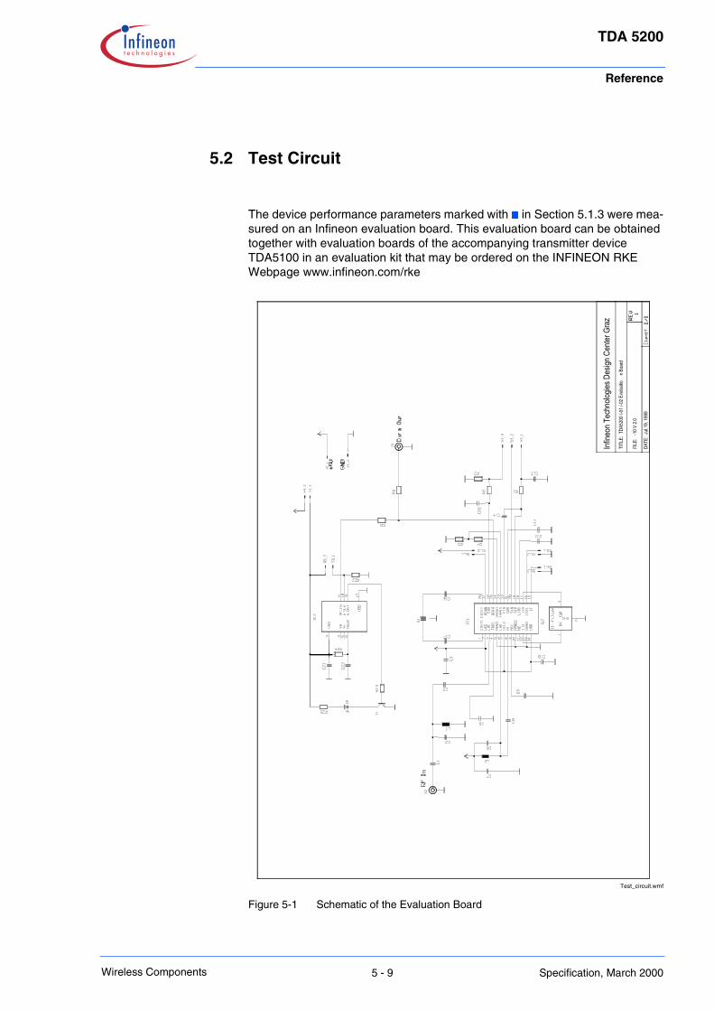
5.2 Test Circuit
The device performance parameters marked with in Section 5.1.3 were mea-sured on an Infineon evaluation board. This evaluation board can be obtained together with evaluation boards of the accompanying transmitter device TDA5100 in an evaluation kit that may be ordered on the INFINEON RKE Webpage www.infineon.com/rke
Test_circuit.wmf
Figure 5-1 Schematic of the Evaluation Board
Infine
on T
echn
ologie
s Des
ign C
enter
Gra
zTI
TLE:
TDA
5200
/-01
/-02
Eva
luatio
n Boa
rd
FILE
: -1
0 V 2.
0
DATE
: Jul.
19, 1
999
5 - 9Wireless Components Specification, March 2000
Reference
TDA 5200
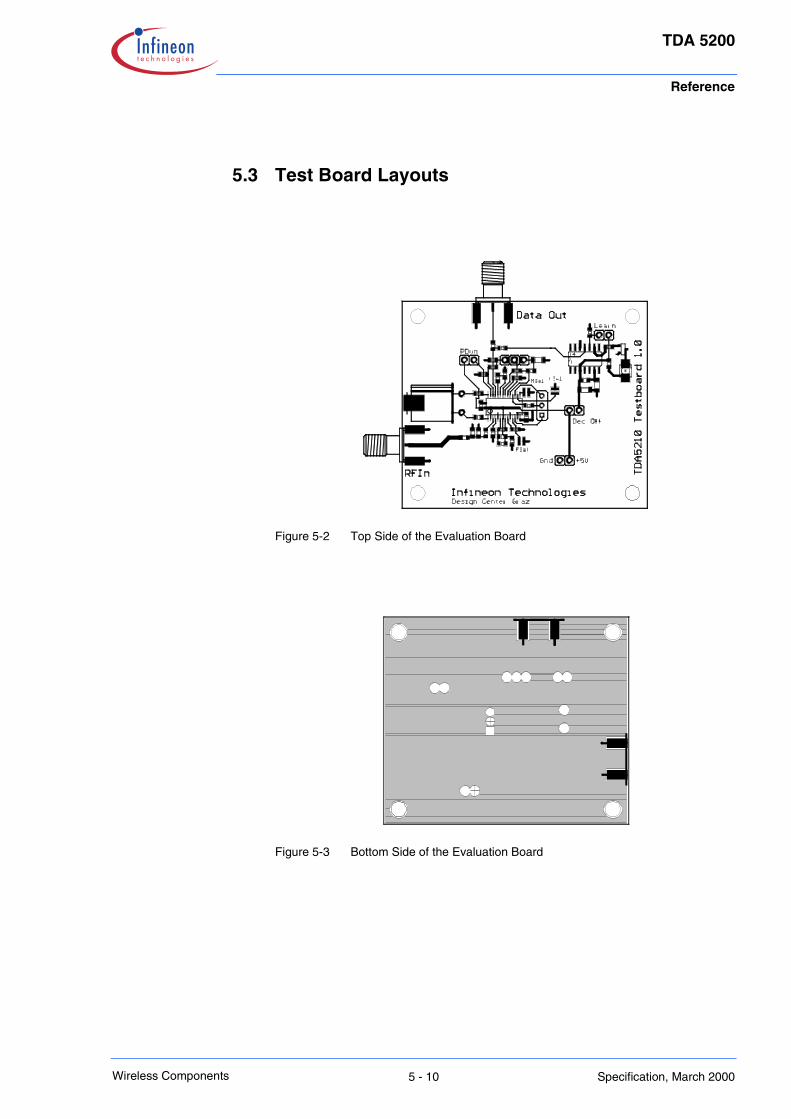
5.3 Test Board Layouts
Figure 5-2 Top Side of the Evaluation Board
Figure 5-3 Bottom Side of the Evaluation Board
5 - 10Wireless Components Specification, March 2000

Reference
TDA 5200
Figure 5-4 Component Placement on the Evaluation Board
5 - 11Wireless Components Specification, March 2000
Reference
TDA 5200
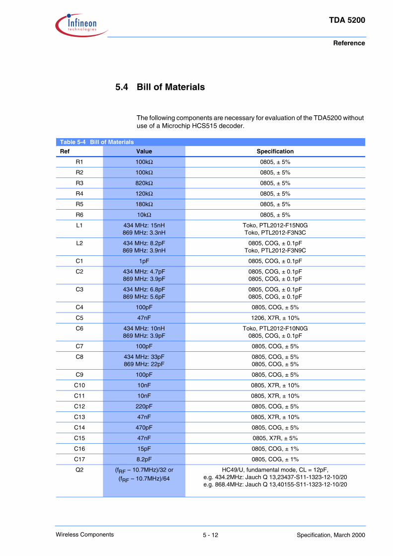
5.4 Bill of Materials
The following components are necessary for evaluation of the TDA5200 without use of a Microchip HCS515 decoder.
Table 5-4 Bill of Materials
Ref Value Specification
R1 100kΩ 0805, ± 5%
R2 100kΩ 0805, ± 5%
R3 820kΩ 0805, ± 5%
R4 120kΩ 0805, ± 5%
R5 180kΩ 0805, ± 5%
R6 10kΩ 0805, ± 5%
L1 434 MHz: 15nH869 MHz: 3.3nH
Toko, PTL2012-F15N0GToko, PTL2012-F3N3C
L2 434 MHz: 8.2pF869 MHz: 3.9nH
0805, COG, ± 0.1pFToko, PTL2012-F3N9C
C1 1pF 0805, COG, ± 0.1pF
C2 434 MHz: 4.7pF869 MHz: 3.9pF
0805, COG, ± 0.1pF0805, COG, ± 0.1pF
C3 434 MHz: 6.8pF869 MHz: 5.6pF
0805, COG, ± 0.1pF0805, COG, ± 0.1pF
C4 100pF 0805, COG, ± 5%
C5 47nF 1206, X7R, ± 10%
C6 434 MHz: 10nH869 MHz: 3.9pF
Toko, PTL2012-F10N0G0805, COG, ± 0.1pF
C7 100pF 0805, COG, ± 5%
C8 434 MHz: 33pF869 MHz: 22pF
0805, COG, ± 5%0805, COG, ± 5%
C9 100pF 0805, COG, ± 5%
C10 10nF 0805, X7R, ± 10%
C11 10nF 0805, X7R, ± 10%
C12 220pF 0805, COG, ± 5%
C13 47nF 0805, X7R, ± 10%
C14 470pF 0805, COG, ± 5%
C15 47nF 0805, X7R, ± 5%
C16 15pF 0805, COG, ± 1%
C17 8.2pF 0805, COG, ± 1%
Q2 (fRF – 10.7MHz)/32 or
(fRF – 10.7MHz)/64
HC49/U, fundamental mode, CL = 12pF, e.g. 434.2MHz: Jauch Q 13,23437-S11-1323-12-10/20e.g. 868.4MHz: Jauch Q 13,40155-S11-1323-12-10/20
5 - 12Wireless Components Specification, March 2000

Reference
TDA 5200
Please note that in case of operation at 434 MHz a capacitor has to be soldered in place of L2 and an inductor in place of C6.
The following components are necessary in addition to the above mentioned ones for evaluation of the TDA52o0 in conjunction with a Microchip HCS515 decoder.
Table 5-4 Bill of materials (continued)
Ref Value Specification
F1 SFE10.7MA5-A orSKM107M1-A20-10
MurataToko
X2, X3 142-0701-801 Johnson
X1, X4, S1, S5 2-pole pin connector
S4 3-pole pin connector, or not equipped
IC1 TDA 5200 Infineon
Table 5-5 Bill of Materials Addendum
Ref Value Specification
R21 22kΩ 0805, ± 5%
R22 100kΩ 0805, ± 5%
R23 22kΩ 0805, ± 5%
R24 820kΩ 0805, ± 5%
R25 560kΩ 0805, ± 5%
C21 100nF 1206, X7R, ± 10%
C22 100nF 1206, X7R, ± 10%
IC2 HCS515 Microchip
T1 BC 847B Infineon
D1 LS T670-JL Infineon
5 - 13Wireless Components Specification, March 2000
List of Figures
List of Figures - 1
TDA 5200
Wireless Components
Specification, March 2000
List of Figures
Figure 2-1 P-TSSOP-28-1 package outlines . . . . . . . . . . . . . . . . . . . . . . . . . . . . . . . . . . . . . . . . . 2-3
Figure 3-1 IC Pin Configuration . . . . . . . . . . . . . . . . . . . . . . . . . . . . . . . . . . . . . . . . . . . . . . . . . . . 3-2
Figure 3-2 Main Block Diagram . . . . . . . . . . . . . . . . . . . . . . . . . . . . . . . . . . . . . . . . . . . . . . . . . . . 3-9
Figure 4-1 LNA Automatic Gain Control Circuitry . . . . . . . . . . . . . . . . . . . . . . . . . . . . . . . . . . . . . . 4-2
Figure 4-2 RSSI Level and Permissive AGC Threshold Levels . . . . . . . . . . . . . . . . . . . . . . . . . . . 4-3
Figure 4-3 Data Filter Design . . . . . . . . . . . . . . . . . . . . . . . . . . . . . . . . . . . . . . . . . . . . . . . . . . . . . 4-4
Figure 4-4 Determination of Series Capacitance Value for the Quartz Oscillator . . . . . . . . . . . . . . 4-5
Figure 4-5 Data Slicer Threshold Generation with External R-C Integrator . . . . . . . . . . . . . . . . . . 4-7
Figure 4-6 Data Slicer Threshold Generation Utilising the Peak Detector . . . . . . . . . . . . . . . . . . . 4-7
Figure 5-1 Schematic of the Evaluation Board . . . . . . . . . . . . . . . . . . . . . . . . . . . . . . . . . . . . . . . . 5-9
Figure 5-2 Top Side of the Evaluation Board . . . . . . . . . . . . . . . . . . . . . . . . . . . . . . . . . . . . . . . . . 5-10
Figure 5-3 Bottom Side of the Evaluation Board . . . . . . . . . . . . . . . . . . . . . . . . . . . . . . . . . . . . . . . 5-10
Figure 5-4 Component Placement on the Evaluation Board . . . . . . . . . . . . . . . . . . . . . . . . . . . . . . 5-11
List of Tables
TDA 5200
List of Tables
Table 3-1 Pin Definition and Function . . . . . . . . . . . . . . . . . . . . . . . . . . . . . . . . . . . . . . . . . . . . . . 3-3
Table 3-4 PDWN pin operating states . . . . . . . . . . . . . . . . . . . . . . . . . . . . . . . . . . . . . . . . . . . . . . 3-12
Table 4-1 PLL Division Ratio Dependence on States of FSEL and CSEL . . . . . . . . . . . . . . . . . . 4-6
Table 5-1 Absolute Maximum Ratings, Ambient temperature TAMB=-40°C ... + 85°C . . . . . . . . . 5-2
Table 5-2 Operating Range, Ambient temperature TAMB= -40°C ... + 85°C . . . . . . . . . . . . . . . . . 5-3
Table 5-3 AC/DC Characteristics with TA 25 °C, VVCC = 8.5 V . . . . . . . . . . . . . . . . . . . . . . . . . . 5-4
Table 5-4 Bill of Materials . . . . . . . . . . . . . . . . . . . . . . . . . . . . . . . . . . . . . . . . . . . . . . . . . . . . . . . 5-12
Table 5-5 Bill of Materials Addendum . . . . . . . . . . . . . . . . . . . . . . . . . . . . . . . . . . . . . . . . . . . . . . 5-13
List of Tables - 1Wireless Components Specification, March 2000
List of Tables
TDA 5200
List of Tables - 2Wireless Components Specification, March 2000
Related Documents