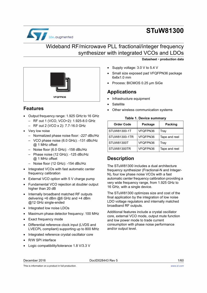
This is information on a product in full production. December 2016 DocID028443 Rev 5 1/60 STuW81300 Wideband RF/microwave PLL fractional/integer frequency synthesizer with integrated VCOs and LDOs Datasheet - production data Features • Output frequency range: 1.925 GHz to 16 GHz – RF out 1 (VCO, VCO÷2): 1.925-8.0 GHz – RF out 2 (VCO x 2): 7.7-16.0 GHz • Very low noise – Normalized phase noise floor: -227 dBc/Hz – VCO phase noise (6.0 GHz): -131 dBc/Hz @ 1 MHz offset – Noise floor (6.0 GHz): -158 dBc/Hz – Phase noise (12 GHz): -125 dBc/Hz @ 1 MHz offset – Noise floor (12 GHz): -154 dBc/Hz • Integrated VCOs with fast automatic center frequency calibration • External VCO option with 5 V charge pump • Fundamental VCO rejection at doubler output higher than 20 dB • Internally broadband matched RF outputs delivering +6 dBm @6 GHz and +4 dBm @12 GHz single-ended • Integrated low noise LDOs • Maximum phase detector frequency: 100 MHz • Exact frequency mode • Differential reference clock input (LVDS and LVECPL compliant) supporting up to 800 MHz • Integrated reference crystal oscillator core • R/W SPI interface • Logic compatibility/tolerance 1.8 V/3.3 V • Supply voltage: 3.0 V to 5.4 V • Small size exposed pad VFQFPN36 package 6x6x1.0 mm • Process: BICMOS 0.25 μm SiGe Applications • Infrastructure equipment • Satellite • Other wireless communication systems Description The STuW81300 includes a dual architecture frequency synthesizer (Fractional-N and Integer- N), four low phase noise VCOs with a fast automatic center frequency calibration providing a very wide frequency range, from 1.925 GHz to 16 GHz, with a single device. The STuW81300 optimizes size and cost of the final application by the integration of low noise LDO voltage regulators and internally matched broadband RF outputs. Additional features include a crystal oscillator core, external VCO mode, output mute function and low power mode to trade current consumption with phase noise performance and/or output level. VFQFPN36 Table 1. Device summary Order Code Package Packing STUW81300-1T VFQFPN36 Tray STUW81300-1TR VFQFPN36 Tape and reel STUW81300T VFQFPN36 Tray STUW81300TR VFQFPN36 Tape and reel www.st.com

Welcome message from author
This document is posted to help you gain knowledge. Please leave a comment to let me know what you think about it! Share it to your friends and learn new things together.
Transcript
This is information on a product in full production.
December 2016 DocID028443 Rev 5 1/60
STuW81300
Wideband RF/microwave PLL fractional/integer frequency synthesizer with integrated VCOs and LDOs
Datasheet - production data
Features
• Output frequency range: 1.925 GHz to 16 GHz
– RF out 1 (VCO, VCO÷2): 1.925-8.0 GHz
– RF out 2 (VCO x 2): 7.7-16.0 GHz
• Very low noise
– Normalized phase noise floor: -227 dBc/Hz
– VCO phase noise (6.0 GHz): -131 dBc/Hz @ 1 MHz offset
– Noise floor (6.0 GHz): -158 dBc/Hz
– Phase noise (12 GHz): -125 dBc/Hz @ 1 MHz offset
– Noise floor (12 GHz): -154 dBc/Hz
• Integrated VCOs with fast automatic center frequency calibration
• External VCO option with 5 V charge pump
• Fundamental VCO rejection at doubler output higher than 20 dB
• Internally broadband matched RF outputs delivering +6 dBm @6 GHz and +4 dBm @12 GHz single-ended
• Integrated low noise LDOs
• Maximum phase detector frequency: 100 MHz
• Exact frequency mode
• Differential reference clock input (LVDS and LVECPL compliant) supporting up to 800 MHz
• Integrated reference crystal oscillator core
• R/W SPI interface
• Logic compatibility/tolerance 1.8 V/3.3 V
• Supply voltage: 3.0 V to 5.4 V
• Small size exposed pad VFQFPN36 package 6x6x1.0 mm
• Process: BICMOS 0.25 µm SiGe
Applications• Infrastructure equipment
• Satellite
• Other wireless communication systems
Description
The STuW81300 includes a dual architecture frequency synthesizer (Fractional-N and Integer- N), four low phase noise VCOs with a fast automatic center frequency calibration providing a very wide frequency range, from 1.925 GHz to 16 GHz, with a single device.
The STuW81300 optimizes size and cost of the final application by the integration of low noise LDO voltage regulators and internally matched broadband RF outputs.
Additional features include a crystal oscillator core, external VCO mode, output mute function and low power mode to trade current consumption with phase noise performance and/or output level.
VFQFPN36
Table 1. Device summary
Order Code Package Packing
STUW81300-1T VFQFPN36 Tray
STUW81300-1TR VFQFPN36 Tape and reel
STUW81300T VFQFPN36 Tray
STUW81300TR VFQFPN36 Tape and reel
www.st.com

Contents STuW81300
2/60 DocID028443 Rev 5
Contents
1 Functional block diagram . . . . . . . . . . . . . . . . . . . . . . . . . . . . . . . . . . . . . 6
2 Pin definitions . . . . . . . . . . . . . . . . . . . . . . . . . . . . . . . . . . . . . . . . . . . . . . 7
3 Absolute maximum ratings . . . . . . . . . . . . . . . . . . . . . . . . . . . . . . . . . . 10
4 Operating conditions . . . . . . . . . . . . . . . . . . . . . . . . . . . . . . . . . . . . . . . 11
5 Electrical specifications . . . . . . . . . . . . . . . . . . . . . . . . . . . . . . . . . . . . . 13
6 Typical performance characteristics . . . . . . . . . . . . . . . . . . . . . . . . . . . 19
7 Circuit description . . . . . . . . . . . . . . . . . . . . . . . . . . . . . . . . . . . . . . . . . . 23
7.1 Reference input stage . . . . . . . . . . . . . . . . . . . . . . . . . . . . . . . . . . . . . . . 23
7.2 Reference divider . . . . . . . . . . . . . . . . . . . . . . . . . . . . . . . . . . . . . . . . . . . 23
7.3 PLL N divider . . . . . . . . . . . . . . . . . . . . . . . . . . . . . . . . . . . . . . . . . . . . . . 24
7.4 Fractional spurs and compensation mechanism . . . . . . . . . . . . . . . . . . . 25
7.4.1 PFD delay mode . . . . . . . . . . . . . . . . . . . . . . . . . . . . . . . . . . . . . . . . . . 26
7.4.2 Charge pump leakage current . . . . . . . . . . . . . . . . . . . . . . . . . . . . . . . . 26
7.4.3 Down-split current . . . . . . . . . . . . . . . . . . . . . . . . . . . . . . . . . . . . . . . . . 26
7.5 Phase frequency detector (PFD) . . . . . . . . . . . . . . . . . . . . . . . . . . . . . . . 27
7.6 Lock detect . . . . . . . . . . . . . . . . . . . . . . . . . . . . . . . . . . . . . . . . . . . . . . . . 27
7.7 Charge pump . . . . . . . . . . . . . . . . . . . . . . . . . . . . . . . . . . . . . . . . . . . . . . 28
7.8 Fast lock mode . . . . . . . . . . . . . . . . . . . . . . . . . . . . . . . . . . . . . . . . . . . . . 28
7.9 Cycle slip reduction . . . . . . . . . . . . . . . . . . . . . . . . . . . . . . . . . . . . . . . . . 29
7.10 Voltage controlled oscillators (VCOs) . . . . . . . . . . . . . . . . . . . . . . . . . . . . 29
7.11 RF output stage . . . . . . . . . . . . . . . . . . . . . . . . . . . . . . . . . . . . . . . . . . . . 30
7.12 Low-power functional modes . . . . . . . . . . . . . . . . . . . . . . . . . . . . . . . . . . 31
7.13 LDO voltage regulators . . . . . . . . . . . . . . . . . . . . . . . . . . . . . . . . . . . . . . 31
7.14 STuW81300 register programming . . . . . . . . . . . . . . . . . . . . . . . . . . . . . 32
7.15 STuW81300 register summary . . . . . . . . . . . . . . . . . . . . . . . . . . . . . . . . . 34
7.16 STuW81300 register descriptions . . . . . . . . . . . . . . . . . . . . . . . . . . . . . . 35
DocID028443 Rev 5 3/60
STuW81300 Contents
3
7.17 Power-on sequence . . . . . . . . . . . . . . . . . . . . . . . . . . . . . . . . . . . . . . . . . 50
7.18 Example register programming . . . . . . . . . . . . . . . . . . . . . . . . . . . . . . . . 50
8 Application information . . . . . . . . . . . . . . . . . . . . . . . . . . . . . . . . . . . . . 51
8.1 Application diagram . . . . . . . . . . . . . . . . . . . . . . . . . . . . . . . . . . . . . . . . . 51
8.2 Thermal PCB design considerations . . . . . . . . . . . . . . . . . . . . . . . . . . . . 52
8.3 Robust VCO calibration over full temperature range . . . . . . . . . . . . . . . . 52
9 Package information . . . . . . . . . . . . . . . . . . . . . . . . . . . . . . . . . . . . . . . . 55
10 Evaluation kit . . . . . . . . . . . . . . . . . . . . . . . . . . . . . . . . . . . . . . . . . . . . . . 57
11 Revision history . . . . . . . . . . . . . . . . . . . . . . . . . . . . . . . . . . . . . . . . . . . 58
List of figures STuW81300
4/60 DocID028443 Rev 5
List of figures
Figure 1. STuW81300 functional block diagram . . . . . . . . . . . . . . . . . . . . . . . . . . . . . . . . . . . . . . . . . 6Figure 2. Top view . . . . . . . . . . . . . . . . . . . . . . . . . . . . . . . . . . . . . . . . . . . . . . . . . . . . . . . . . . . . . . . . 7Figure 3. VCO open loop phase noise (5 V supply). . . . . . . . . . . . . . . . . . . . . . . . . . . . . . . . . . . . . . 19Figure 4. Closed loop phase noise (5 V supply) . . . . . . . . . . . . . . . . . . . . . . . . . . . . . . . . . . . . . . . . 19Figure 5. VCO Open loop phase noise at 5.3 GHz vs. supply . . . . . . . . . . . . . . . . . . . . . . . . . . . . . . 19Figure 6. VCO open loop phase noise over Frequency vs. supply . . . . . . . . . . . . . . . . . . . . . . . . . . 19Figure 7. Single sideband integrated phase noise vs. frequency and supply (FPFD=50 MHz) . . . . . 20Figure 8. Average KVCO over VCO frequency and supply. . . . . . . . . . . . . . . . . . . . . . . . . . . . . . . . . 20Figure 9. Phase noise and fractional spurs at 5952.5 MHz vs supply (FPFD=50 MHz) . . . . . . . . . . . 20Figure 10. Phase noise and fractional spurs at 11502.5 MHz vs supply (FPFD=50 MHz) . . . . . . . . . . 20Figure 11. Output power level vs temperature – RF1 output (5.0 V supply) . . . . . . . . . . . . . . . . . . . . 20Figure 12. Output power level vs temperature– RF2 output (5.0 V supply) . . . . . . . . . . . . . . . . . . . . . 20Figure 13. VCO feedthrough at RF2 output vs. fundamental VCO frequency . . . . . . . . . . . . . . . . . . . 21Figure 14. Typical spur level vs offset from 12 GHz (5.0 V supply, FPFD=50 MHz). . . . . . . . . . . . . . . 21Figure 15. Typical spur level at PFD offset over carrier frequency (5.0 V supply) . . . . . . . . . . . . . . . . 21Figure 16. 10 kHz and 2.5 MHz fractional spur (integer boundary, 5.0 V supply, FPFD=50 MHz) . . . . 21Figure 17. Frequency settling with vco calibration – wideband view . . . . . . . . . . . . . . . . . . . . . . . . . . 21Figure 18. Frequency settling with VCO calibration – narrowband view . . . . . . . . . . . . . . . . . . . . . . . 21Figure 19. Overall current consumption vs temperature (5.0 V supply, FPFD=50 MHz) . . . . . . . . . . . 22Figure 20. Overall current consumption vs temperature (3.6 V supply, FPFD=50 MHz) . . . . . . . . . . . 22Figure 21. Figure of merit. . . . . . . . . . . . . . . . . . . . . . . . . . . . . . . . . . . . . . . . . . . . . . . . . . . . . . . . . . . 22Figure 22. Reference clock buffer configurations: single-ended (A),
differential (B), crystal mode (C) . . . . . . . . . . . . . . . . . . . . . . . . . . . . . . . . . . . . . . . . . . . . . 23Figure 23. PFD diagram. . . . . . . . . . . . . . . . . . . . . . . . . . . . . . . . . . . . . . . . . . . . . . . . . . . . . . . . . . . . 27Figure 24. SPI Protocol . . . . . . . . . . . . . . . . . . . . . . . . . . . . . . . . . . . . . . . . . . . . . . . . . . . . . . . . . . . . 32Figure 25. SPI timing diagram . . . . . . . . . . . . . . . . . . . . . . . . . . . . . . . . . . . . . . . . . . . . . . . . . . . . . . . 33Figure 26. Application diagram . . . . . . . . . . . . . . . . . . . . . . . . . . . . . . . . . . . . . . . . . . . . . . . . . . . . . . 51Figure 27. VFQFPN36 package outline . . . . . . . . . . . . . . . . . . . . . . . . . . . . . . . . . . . . . . . . . . . . . . . . 55

DocID028443 Rev 5 5/60
STuW81300 List of tables
5
List of tables
Table 1. Device summary . . . . . . . . . . . . . . . . . . . . . . . . . . . . . . . . . . . . . . . . . . . . . . . . . . . . . . . . . . 1Table 2. Pin descriptions . . . . . . . . . . . . . . . . . . . . . . . . . . . . . . . . . . . . . . . . . . . . . . . . . . . . . . . . . . 8Table 3. Absolute maximum ratings . . . . . . . . . . . . . . . . . . . . . . . . . . . . . . . . . . . . . . . . . . . . . . . . . 10Table 4. Operating conditions. . . . . . . . . . . . . . . . . . . . . . . . . . . . . . . . . . . . . . . . . . . . . . . . . . . . . . 11Table 5. Digital logic levels . . . . . . . . . . . . . . . . . . . . . . . . . . . . . . . . . . . . . . . . . . . . . . . . . . . . . . . . 12Table 6. Electrical specifications. . . . . . . . . . . . . . . . . . . . . . . . . . . . . . . . . . . . . . . . . . . . . . . . . . . . 13Table 7. Phase noise specifications . . . . . . . . . . . . . . . . . . . . . . . . . . . . . . . . . . . . . . . . . . . . . . . . . 17Table 8. Current value vs. selection . . . . . . . . . . . . . . . . . . . . . . . . . . . . . . . . . . . . . . . . . . . . . . . . . 28Table 9. SPI timings . . . . . . . . . . . . . . . . . . . . . . . . . . . . . . . . . . . . . . . . . . . . . . . . . . . . . . . . . . . . . 33Table 10. SPI Register map (address 12 to 15 not available) . . . . . . . . . . . . . . . . . . . . . . . . . . . . . . 34Table 11. Example of data for robust VCO calibration routine to be stored
in the application memory. . . . . . . . . . . . . . . . . . . . . . . . . . . . . . . . . . . . . . . . . . . . . . . . . . 54Table 12. VFQFPN36 package mechanical data . . . . . . . . . . . . . . . . . . . . . . . . . . . . . . . . . . . . . . . . 56Table 13. STuW81300 evaluation-kit order codes . . . . . . . . . . . . . . . . . . . . . . . . . . . . . . . . . . . . . . . 57Table 14. Document revision history . . . . . . . . . . . . . . . . . . . . . . . . . . . . . . . . . . . . . . . . . . . . . . . . . 58

Functional block diagram STuW81300
6/60 DocID028443 Rev 5
1 Functional block diagram
Figure 1. STuW81300 functional block diagram
DocID028443 Rev 5 7/60
STuW81300 Pin definitions
56
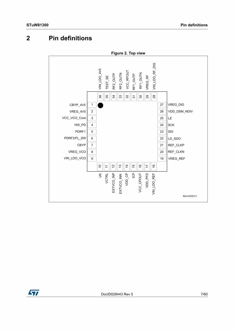
2 Pin definitions
Figure 2. Top view

Pin definitions STuW81300
8/60 DocID028443 Rev 5
Table 2. Pin descriptions
Pin No Name Description Observation
1 CBYP_4V5 Connection for 4.5 V regulator bypass capacitor -
2 VREG_4V5 Regulated output voltage of 4.5 V regulator -
3 VCC_VCO_Core Supply voltage of VCO CoreMust be connected to VREG_4V5
4 HW_PD HW Power DownCMOS Schmitt Triggered Input, 1.8 V compatible, 3.3 V tolerant
5 PDRF1 RF1 output stage Power Down controlCMOS Schmitt Triggered Input, 1.8 V compatible, 3.3 V tolerant
6 PDRF2/FL_SWRF2 output stage Power Down control / Fast-Lock switch
CMOS Schmitt Triggered Input, 1.8 V compatible, 3.3 V tolerant. Can be also used as switch for fast-lock loop filter configuration
7 CBYP Connection of VCO regulator bypass capacitor -
8 VREG_VCORegulated output voltage of VCO circuitry regulator
-
9 VIN_LDO_VCO Supply voltage of VCO circuitry regulator -
10 VRConnection of reference voltage filtering capacitor
-
11 VCTRL VCO control voltage -
12 EXTVCO_INP External VCO positive inputMust be connected to ground if external VCO is not used
13 EXTVCO_INN External VCO negative inputMust be connected to ground if external VCO is not used
14 VDD_CP Digital charge-pump supply voltageMust be connected to VREG_VCO
15 ICP PLL charge pump output -
16 VCC_CPOUT Supply voltage for Charge Pump output stageMust be connected to VREG_4V5
17 VDD_PFDSupply voltage of digital phase/frequency detector
Must be connected to VREG_REF
18 VIN_LDO_REF Supply voltage for reference clock regulator -
19 VREG_REF Regulated supply voltage of PLL -
20 REF_CLKN Reference clock negative input -
21 REF_CLKP Reference clock positive input -
22 LD_SDO Lock Detector / SPI Data outputCMOS push-pull Output 2.5 V with slew rate control or open drain (1.8 V to 3.3 V tolerant)
23 SDI SPI Data inputCMOS Schmitt triggered Input, 1.8 V compatible, 3.3 V tolerant
24 SCK SPI clockCMOS Schmitt triggered Input, 1.8 V compatible, 3.3 V tolerant

DocID028443 Rev 5 9/60
STuW81300 Pin definitions
56
25 LE SPI load enableCMOS Schmitt triggered Input, 1.8 V compatible, 3.3 V tolerant
26 VDD_DSM_NDIVSupply voltage of Delta-Sigma modulator and loop divider
Must be connected to VREG_DIG
27 VREG_DIG Regulated supply voltage of digital circuitry -
28 VIN_LDO_RF_DIGSupply voltage of RF and digital circuitry regulators
-
29 VREG_RF Regulated supply voltage of RF blocks -
30 RF1_OUTN Direct and divided by 2 negative output Internally matched to 50 ohm
31 RF1_OUTP Direct and divided by 2 positive output Internally matched to 50 ohm
32 VCC_RFOUT Supply voltage for RF output stagesMust be connected to VREG_4V5
33 RF2_OUTN Doubler negative output Internally matched to 50 ohm
34 RF2_OUTP Doubler positive output Internally matched to 50 ohm
35 TEST_SE Test pin Must be connected to GND
36 VIN_LDO_4V5 Supply voltage of 4.5V regulator -
Table 2. Pin descriptions (continued)
Pin No Name Description Observation

Absolute maximum ratings STuW81300
10/60 DocID028443 Rev 5
3 Absolute maximum ratings
Table 3. Absolute maximum ratings
Symbol Parameter Value Unit
VCC Supply voltage (LDO input pins #9, 18, 28, 36) -0.3 to 5.4 V
Tstg Storage temperature +150 °C
ESD
Electrical Static Discharge
– HBM(1)
– CDM-JEDEC Standard
2
0.5
kV
1. The maximum rating of the ESD protection circuitry on pin 21 (REF_CLKP) is 1.5 kV.
DocID028443 Rev 5 11/60
STuW81300 Operating conditions
56
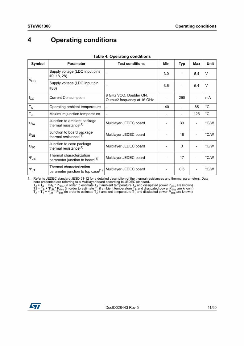
4 Operating conditions
Table 4. Operating conditions
Symbol Parameter Test conditions Min Typ Max Unit
VCC
Supply voltage (LDO input pins #9, 18, 28)
- 3.0 - 5.4 V
Supply voltage (LDO input pin
#36)- 3.6 - 5.4 V
ICC Current Consumption8 GHz VCO, Doubler ON,
Output2 frequency at 16 GHz
- 290 - mA
TA Operating ambient temperature - -40 - 85 °C
TJ Maximum junction temperature - - - 125 °C
ΘJAJunction to ambient package thermal resistance(1) Multilayer JEDEC board - 33 - °C/W
ΘJBJunction to board package thermal resistance(1) Multilayer JEDEC board - 18 - °C/W
ΘJCJunction to case package thermal resistance(1) Multilayer JEDEC board - 3 - °C/W
ΨJBThermal characterization parameter junction to board(1) Multilayer JEDEC board - 17 - °C/W
ΨJTThermal characterization parameter junction to top case(1) Multilayer JEDEC board - 0.5 - °C/W
1. Refer to JEDEC standard JESD 51-12 for a detailed description of the thermal resistances and thermal parameters. Data here presented are referring to a Multilayer board according to JEDEC standard. TJ = TA + ΘJA * Pdiss (in order to estimate TJ if ambient temperature TA and dissipated power Pdiss are known) TJ = TB + ΨJB * Pdiss (in order to estimate TJ if ambient temperature TB and dissipated power Pdiss are known) TJ = TT + ΨJT * Pdiss (in order to estimate TJ if ambient temperature TT and dissipated power Pdiss are known)

Operating conditions STuW81300
12/60 DocID028443 Rev 5
Table 5. Digital logic levels
Symbol Parameter Test conditions Min Typ Max Unit
Vdd Internal Supply for digital circuits - - 2.6 - V
Vil Low level input voltage Schmitt input 0 - 0.6 V
Vih High level input voltage Schmitt input 1.2 - 3.6 V
Vol Low level output voltage IOL = 4 mA - - 0.2 V
Voh High level output voltage IOH = 4 mA Vdd-0.2 - - V
DocID028443 Rev 5 13/60
STuW81300 Electrical specifications
56
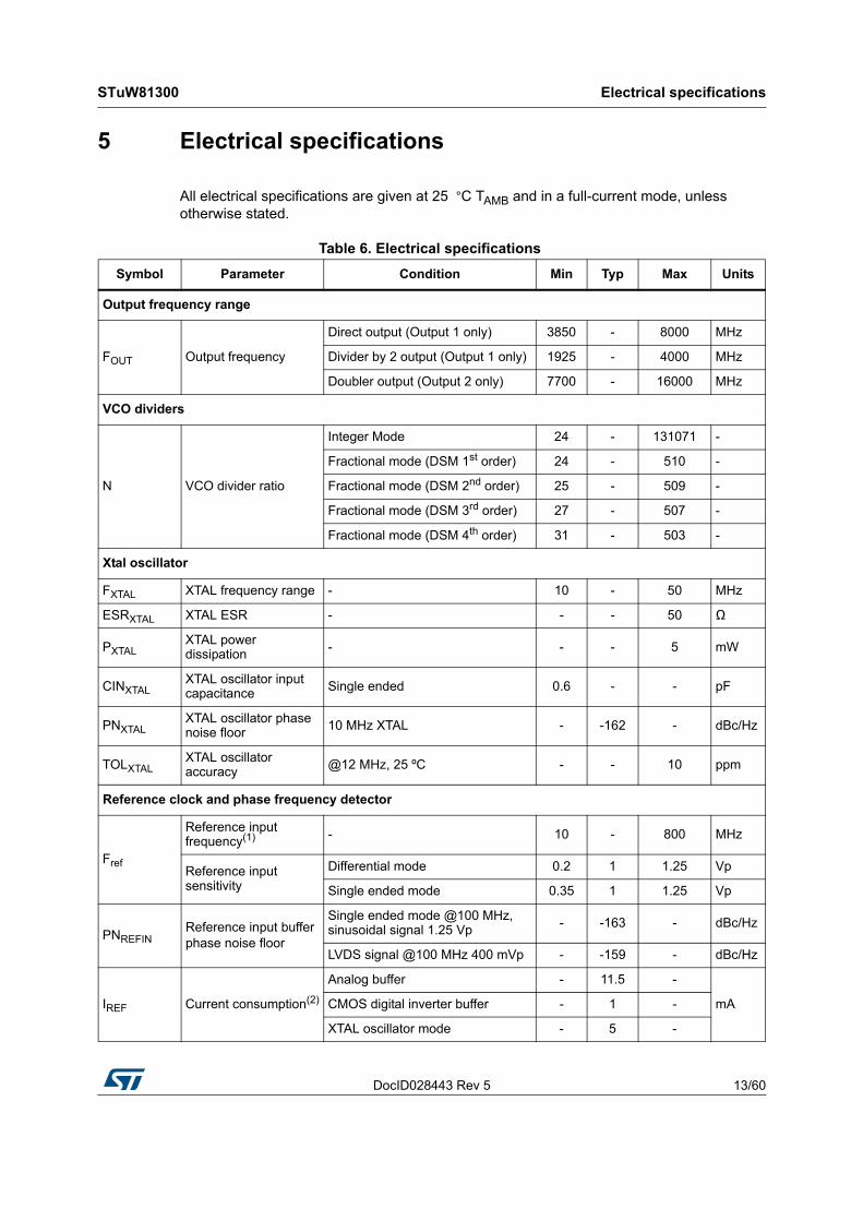
5 Electrical specifications
All electrical specifications are given at 25 °C TAMB and in a full-current mode, unless otherwise stated.
Table 6. Electrical specifications
Symbol Parameter Condition Min Typ Max Units
Output frequency range
FOUT Output frequency
Direct output (Output 1 only) 3850 - 8000 MHz
Divider by 2 output (Output 1 only) 1925 - 4000 MHz
Doubler output (Output 2 only) 7700 - 16000 MHz
VCO dividers
N VCO divider ratio
Integer Mode 24 - 131071 -
Fractional mode (DSM 1st order) 24 - 510 -
Fractional mode (DSM 2nd order) 25 - 509 -
Fractional mode (DSM 3rd order) 27 - 507 -
Fractional mode (DSM 4th order) 31 - 503 -
Xtal oscillator
FXTAL XTAL frequency range - 10 - 50 MHz
ESRXTAL XTAL ESR - - - 50 Ω
PXTALXTAL power dissipation - - - 5 mW
CINXTALXTAL oscillator input capacitance Single ended 0.6 - - pF
PNXTALXTAL oscillator phase noise floor 10 MHz XTAL - -162 - dBc/Hz
TOLXTALXTAL oscillator accuracy @12 MHz, 25 ºC - - 10 ppm
Reference clock and phase frequency detector
Fref
Reference input frequency(1) - 10 - 800 MHz
Reference input sensitivity
Differential mode 0.2 1 1.25 Vp
Single ended mode 0.35 1 1.25 Vp
PNREFINReference input buffer phase noise floor
Single ended mode @100 MHz, sinusoidal signal 1.25 Vp - -163 - dBc/Hz
LVDS signal @100 MHz 400 mVp - -159 - dBc/Hz
IREF Current consumption(2)
Analog buffer - 11.5 -
mACMOS digital inverter buffer - 1 -
XTAL oscillator mode - 5 -

Electrical specifications STuW81300
14/60 DocID028443 Rev 5
R Reference divider ratio - 1 - 8191
FPFD PFD input frequency(3) - - - 100 MHz
FSTEP Frequency step(3)
LO direct output - 47.5 - Hz
LO with divider by 2 - 23.75 - Hz
LO with doubler - 95 - Hz
Charge pump
ICP ICP sink/source 5-bit programmable - - 4.9 mA
VOCPOutput voltage range on ICP pin (pin#14) - 0.4 -
VCCCPOUT-0.4 V
-Comparison frequency Spurs (4)(5) VCO on output 1 - -85 -
dBc
- In-band fractional spurs (5)(6) VCO on output 1 - -50 -
VCOs
IVCOCoreOscillator core current consumption @ 4 GHz and 4.5 V supply - 57 - mA
IVCOBUFVCO buffer consumption - - 16 - mA
KVCO
VCO gain @4.5 V supply - - 30-85 -
MHz/VVCO gain @3.3 V supply - - 50-105 -
ΔTLOCK - FVCO ≤ 5500MHz, VCC_VCO_Core = 3.3 V(7)(8)
ΔTFALL
Temperature variation, falling temperature
TJ max = 100 °C 110 - - ºC
ΔTRISE
Temperature variation, rising temperature
TJ max = 100 °C 95 - - ºC
ΔTLOCK - FVCO > 5500MHz, VCC_VCO_Core = 3.3 V(7)(8)
ΔTFALL
Temperature variation, falling temperature
TJ max = 100 °C 100 - - ºC
ΔTRISE
Temperature variation, rising temperature
TJ max = 80 °C 85 - - ºC
TJ max = 90 °C 80 - - ºC
TJ max = 100 °C 75 - - ºC
ΔTLOCK - FVCO ≤ 6800MHz, VCC_VCO_Core = 4.5 V(7)(8)
ΔTFALLTemperature variation, falling temperature
TJ max = 100 °C 110 - - °C
ΔTRISETemperature variation, rising temperature
TJ max = 100 °C 95 - - °C
Table 6. Electrical specifications (continued)
Symbol Parameter Condition Min Typ Max Units

DocID028443 Rev 5 15/60
STuW81300 Electrical specifications
56
ΔTLOCK - FVCO > 6800MHz, VCC_VCO_Core = 4.5 V(7)(8)
ΔTFALLTemperature variation, falling temperature
TJ max = 100 °C 110 - - °C
ΔTRISETemperature variation, rising temperature
TJ max = 80 °C 90 - -
°CTJ max = 90 °C 80 - -
TJ max = 100 °C 75 - -
RF output stage
POUT Output level
1.925 GHz to 8 GHz (Output 1 only single ended)
+2 - +8
dBm7.7 GHz to 16 GHz (Output 2 only single ended)
-1 - +5
ZOUT Output impedanceDifferential - 100 -
ΩSingle-ended - 50 -
RL Return loss Matched to 50 ohm - 10 - dB
-Unwanted harmonic Spur leakage(9) Differential output (output 1 and 2) - -20 - dBc
IRFOUTBUFRF output buffer current consumption
1.925 GHz to 8 GHz (+5 dBm output power) - 25 -
mA7.7 GHz to 16 GHz (+3 dBm output power) - 35 -
PLL miscellaneous
IPLLPLL current consumption(10) Prescaler, digital dividers, misc. - 16 - mA
IDSMΔΣ modulator current consumption(10) - - 3.5 - mA
1. The maximum frequency of the Reference Divider is 200 MHz; when using higher reference clock frequency (up to the max. value of 800 MHz) the internal divider by 2 or divider by 4 must be enabled. The fractional mode is allowed in the full frequency range only with reference clock frequency >11.93 MHz With reference clock frequency in the range 10 MHz to 11.93 MHz, due to the limits of N value in fractional mode, the full VCO frequencies would not be addressed in fractional mode; in this case the frequency doubler in the reference path can be enabled.
2. Reference clock signal @ 100 MHz, R=2.
3. The minimum frequency step is obtained as FPFD / (221); these typical values are obtained considering FPFD = 100 MHz.
4. PFD frequency leakage.
5. For VCO divided by 2 (Output 1) subtract 6dB; for VCO doubled (Output 2) add 6dB.
6. This is the level within the PLL loop bandwidth due to the contribution of the ΔΣ Modulator. In order to obtain the fractional spurs level for a specific frequency offset outside the PLL bandwidth, the attenuation provided by the loop filter at such offset should be subtracted.
7. ΔTLOCK expresses the temperature variation for which the device maintains locking condition when programmed at any operative temperature, provided that the initial and final TJ stays between -40 °C and the specified TJ max. No phase jump occurs when changing temperature while the device is in the locked condition (typical temperature change rate around 0.5 ºC/min). Guaranteed by design and characterization. For additional information please refer Section 8.3: Robust VCO calibration over full temperature range.
Table 6. Electrical specifications (continued)
Symbol Parameter Condition Min Typ Max Units

Electrical specifications STuW81300
16/60 DocID028443 Rev 5
8. ΔTLOCK figures reported are given with CAL_TEMP_COMP (ST6 Register) set to’1’ and under the following conditions: When VCO core is supplied at 4.5V: - For FVCO ≤ 4500MHz VCALB_MODE (ST4 Register) MUST be set to ‘0’ - For FVCO > 4500MHz VCALB_MODE (ST4 Register) MUST be set to ‘1’ - CALB_3V3_MODE1 (ST4 Register) must be set to ‘0’ - CALB_3V3_MODE0 (ST4 Register) must be set to ‘0’.
When VCO core is supplied at 3.3V: -For any FVCO VCALB_MODE (ST4 Register) MUST be set to ‘1’ - CALB_3V3_MODE1 (ST4 Register) MUST be set to ‘1’ - CALB_3V3_MODE0 (ST4 Register) MUST be set to ‘1’.
ΔTLOCK data for VCO core supplied at 3.3 V are not available / applicable on product codes STuW81300-1T, STuW81300-1TR.
9. Includes VCO fundamental and higher order harmonics.
10. Current consumption measured with PLL locked in following conditions: Reference clock signal @ 100 MHz; PFD @50 MHz (R=2); VCO @ 4005 MHz.

DocID028443 Rev 5 17/60
STuW81300 Electrical specifications
56
Table 7. Phase noise specifications
Parameter(1) Condition Min Typ Max Units
In-band phase noise floor
Normalized in-band phase noise floor(2)
ICP=5 mA, PLL BW=150 kHz;
including reference divider contribution
- -227 - dBc/Hz
VCO direct - Open Loop @ 3850 MHz
Phase Noise @ 1 kHz
VCC_VCO_Core = 4.5 V
- -62 - dBc/Hz
Phase Noise @ 10 kHz - -92 - dBc/Hz
Phase Noise @ 100 kHz - -114 - dBc/Hz
Phase Noise @ 1 MHz - -135 - dBc/Hz
Phase Noise @ 10 MHz - -153 - dBc/Hz
Phase Noise @ 90 MHz - -160 - dBc/Hz
VCO direct - Open Loop @ 6000 MHz
Phase Noise @ 1 kHz
VCC_VCO_Core = 4.5 V
- -57 - dBc/Hz
Phase Noise @ 10 kHz - -87 - dBc/Hz
Phase Noise @ 100 kHz - -110 - dBc/Hz
Phase Noise @ 1 MHz - -131 - dBc/Hz
Phase Noise @ 10 MHz - -150 - dBc/Hz
Phase Noise @ 90 MHz - -158 - dBc/Hz
VCO direct - Open Loop @ 8000 MHz
Phase Noise @ 1 kHz
VCC_VCO_Core = 4.5 V
- -56 - dBc/Hz
Phase Noise @ 10 kHz - -84 - dBc/Hz
Phase Noise @ 100 kHz - -107 - dBc/Hz
Phase Noise @ 1 MHz - -128 - dBc/Hz
Phase Noise @ 10 MHz - -147 - dBc/Hz
Phase Noise @ 90 MHz - -157 - dBc/Hz
VCO and frequency doubler- Open Loop @ 7700 MHz
Phase Noise @ 1 kHz
VCC_VCO_Core = 4.5 V
- -56 - dBc/Hz
Phase Noise @ 10 kHz - -86 - dBc/Hz
Phase Noise @ 100 kHz - -108 - dBc/Hz
Phase Noise @ 1 MHz - -129 - dBc/Hz
Phase Noise @ 10 MHz - -147 - dBc/Hz
Phase Noise @ 90 MHz - -154 - dBc/Hz

Electrical specifications STuW81300
18/60 DocID028443 Rev 5
VCO and frequency doubler- Open Loop @ 12 GHz
Phase Noise @ 1 kHz
VCC_VCO_Core = 4.5 V
- -51 - dBc/Hz
Phase Noise @ 10 kHz - -81 - dBc/Hz
Phase Noise @ 100 kHz - -104 - dBc/Hz
Phase Noise @ 1 MHz - -125 - dBc/Hz
Phase Noise @ 10 MHz - -144 - dBc/Hz
Phase Noise @ 90 MHz - -154 - dBc/Hz
VCO and frequency doubler - Open Loop @ 16 GHz
Phase Noise @ 1 kHz
VCC_VCO_Core = 4.5 V
- -50 - dBc/Hz
Phase Noise @ 10 kHz - -78 - dBc/Hz
Phase Noise @ 100 kHz - -101 - dBc/Hz
Phase Noise @ 1 MHz - -122 - dBc/Hz
Phase Noise @ 10 MHz - -141 - dBc/Hz
Phase Noise @ 90 MHz - -154 - dBc/Hz
VCO direct – Open loop @ 6 GHz
Phase Noise @ 1 kHz
VCC_VCO_Core = 3.3 V
- -55 - dBc/Hz
Phase Noise @ 10 kHz - -84 - dBc/Hz
Phase Noise @ 100 kHz - -107.5 - dBc/Hz
Phase Noise @ 1 MHz - -128.5 - dBc/Hz
Phase Noise @ 10 MHz - -148.5 - dBc/Hz
Phase Noise @ 90 MHz - -158 - dBc/Hz
VCO and frequency doubler – Open Loop @ 12 GHz
Phase Noise @ 1 kHz
VCC_VCO_Core = 3.3 V
- -49 - dBc/Hz
Phase Noise @ 10 kHz - -78 - dBc/Hz
Phase Noise @ 100 kHz - -101.5 - dBc/Hz
Phase Noise @ 1 MHz - -122.5 - dBc/Hz
Phase Noise @ 10 MHz - -142.5 - dBc/Hz
Phase Noise @ 90 MHz - -155 - dBc/Hz
1. SSB phase noise unless otherwise specified.
2. Normalized PN = Measured PN – 20log(N) – 10log(FPFD) where N is the VCO divider ratio and FPFD is the comparison frequency at the PFD input.
Table 7. Phase noise specifications (continued)
Parameter(1) Condition Min Typ Max Units

DocID028443 Rev 5 19/60
STuW81300 Typical performance characteristics
56
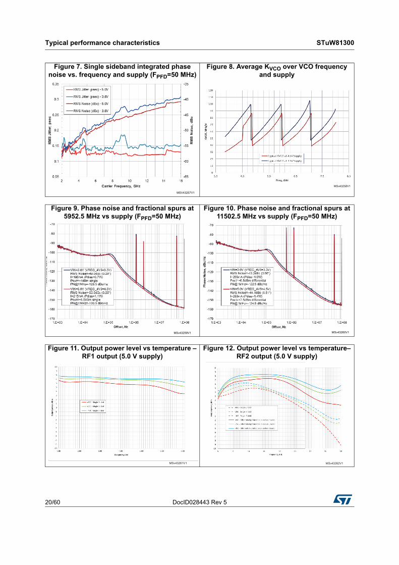
6 Typical performance characteristics
Figure 3. VCO open loop phase noise (5 V supply)
Figure 4. Closed loop phase noise (5 V supply)
Figure 5. VCO Open loop phase noise at 5.3 GHz vs. supply
Figure 6. VCO open loop phase noise over Frequency vs. supply
Typical performance characteristics STuW81300
20/60 DocID028443 Rev 5
Figure 7. Single sideband integrated phase noise vs. frequency and supply (FPFD=50 MHz)
Figure 8. Average KVCO over VCO frequency and supply
Figure 9. Phase noise and fractional spurs at 5952.5 MHz vs supply (FPFD=50 MHz)
Figure 10. Phase noise and fractional spurs at 11502.5 MHz vs supply (FPFD=50 MHz)
Figure 11. Output power level vs temperature – RF1 output (5.0 V supply)
Figure 12. Output power level vs temperature– RF2 output (5.0 V supply)

DocID028443 Rev 5 21/60
STuW81300 Typical performance characteristics
56
Figure 13. VCO feedthrough at RF2 output vs. fundamental VCO frequency
Figure 14. Typical spur level vs offset from 12 GHz (5.0 V supply, FPFD=50 MHz)
Figure 15. Typical spur level at PFD offset over carrier frequency (5.0 V supply)
Figure 16. 10 kHz and 2.5 MHz fractional spur (integer boundary, 5.0 V supply, FPFD=50 MHz)
Figure 17. Frequency settling with vco calibration – wideband view
Figure 18. Frequency settling with VCO calibration – narrowband view

Typical performance characteristics STuW81300
22/60 DocID028443 Rev 5
Figure 19. Overall current consumption vs temperature (5.0 V supply, FPFD=50 MHz)
Figure 20. Overall current consumption vs temperature (3.6 V supply, FPFD=50 MHz)
Figure 21. Figure of merit
DocID028443 Rev 5 23/60
STuW81300 Circuit description
56
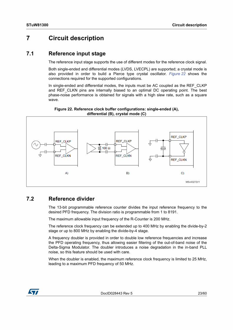
7 Circuit description
7.1 Reference input stage
The reference input stage supports the use of different modes for the reference clock signal.
Both single-ended and differential modes (LVDS, LVECPL) are supported; a crystal mode is also provided in order to build a Pierce type crystal oscillator. Figure 22 shows the connections required for the supported configurations.
In single-ended and differential modes, the inputs must be AC coupled as the REF_CLKP and REF_CLKN pins are internally biased to an optimal DC operating point. The best phase-noise performance is obtained for signals with a high slew rate, such as a square wave.
Figure 22. Reference clock buffer configurations: single-ended (A), differential (B), crystal mode (C)
7.2 Reference divider
The 13-bit programmable reference counter divides the input reference frequency to the desired PFD frequency. The division ratio is programmable from 1 to 8191.
The maximum allowable input frequency of the R-Counter is 200 MHz.
The reference clock frequency can be extended up to 400 MHz by enabling the divide-by-2 stage or up to 800 MHz by enabling the divide-by-4 stage.
A frequency doubler is provided in order to double low reference frequencies and increase the PFD operating frequency, thus allowing easier filtering of the out-of-band noise of the Delta-Sigma Modulator. The doubler introduces a noise degradation in the in-band PLL noise, so this feature should be used with care.
When the doubler is enabled, the maximum reference clock frequency is limited to 25 MHz, leading to a maximum PFD frequency of 50 MHz.
Circuit description STuW81300
24/60 DocID028443 Rev 5
7.3 PLL N divider
The N divider sets the division ratio in the PLL feedback path.
Both Integer-N and Fractional-N PLL architectures are implemented in order to ensure the best overall performance of the synthesizer.
The Fractional-N division is achieved by combining the integer divider section with a Delta-Sigma modulator (DSM), which sets the fractional part of the overall division ratio.
The DSM is implemented as a MASH structure with programmable order (2 bit; 1st, 2nd, 3rd
and 4th order), programmable MODULUS (21 bit).
It also includes a DITHERING function (1 bit), which can be used to reduce fractional spur tones by spreading the DSM sequence and consequently the energy of the spurs over a wider bandwidth.
The overall division ratio, N is given by:
The integer part NINT is 17-bit programmable and can range from 24 to 131071 in Integer Mode. For NINT ≥ 512 the fractional mode is not allowed and the setting used for DSM has no effect.
Based upon the selected order of the Delta-Sigma modulator the allowed range of NINTvalues changes as follows:
• 24 to 510 - 1st Order DSM
• 25 to 509 - 2nd Order DSM
• 27 to 507 - 3rd Order DSM
• 31 to 503 - 4th Order DSM
The fractional part NFRAC of the division ratio is controlled by setting the values FRAC and MOD (21 bits each). It also depends on the value of DITHERING (1 bit):
The MOD value can range from 2 to 2097151, while the range of FRAC is from 0 to MOD-1. If the DITHERING function is not used (DITHERING=0) the fractional part of N is simply derived as the ratio FRAC over MOD.
N NINT NFRAC+=
NFRACFRACMOD-----------------
DITHERING2 MOD⋅
-----------------------------------+=

DocID028443 Rev 5 25/60
STuW81300 Circuit description
56
The resulting VCO frequency is:
where:
FVCO is the output frequency of VCO
Fref is the input reference frequency
R is the division ratio of reference chain
N is the overall division ratio of the PLL
The N divider accepts input signal frequencies up to a maximum of 6 GHz. When the setup requires a VCO frequency greater than 6 GHz, the VCO signal provided to the N divider must be divided by 2 by setting PLL_SEL=’1’ in the ST1 Register . In this case the VCO frequency is fixed by:
The implementation with programmable modulus allows the user to easily select the desired fraction and the exact synthesized frequency with no approximation.
The MOD value can be set to very high values, thus the frequency resolution of the synthesizer can reach very fine steps (down to a few hertz).
A ‘low spur mode’ could be configured by maximizing both FRAC and MOD values, keeping the same desired FRAC/MOD ratio, and setting the DITHERING bit to ‘1’. The drawback is a small frequency error, equal to FPFD/(2*MOD) on the synthesized frequency. This error is in the range of a few hertz (usually tolerated by most applications).
7.4 Fractional spurs and compensation mechanism
The fractional PLL operation generates unwanted fractional spurs around the synthesized frequency.
The integer boundary spurs occur when the carrier frequency is close to an integer multiple of the PFD frequency. If the frequency difference between the carrier and the N*FPFD falls within the PLL loop bandwidth, the integer boundary spur is unfiltered and represents the worst-case situation giving the highest spur level.
The channel spurs are generated by the delta-sigma modulator operations and depend on its settings (they are mainly related to the MOD value). The channel spurs appear at a frequency offset from the carrier, equal to FPFD/MOD and its harmonics, and they are not integer boundary. If the MOD value is extremely high (close to the maximum value of 221-1) the channel spur offset is of the order of a tenth of a hertz and it appears as ‘granular noise’ shaped by the PLL around the carrier.
FVCO
Fref
R---------- N⋅
Fref
R---------- NINT
FRACMOD-----------------
DITHERING2 MOD⋅
-----------------------------------+ + ⋅= =
FVCO
Fref
R---------- 2 NINT
FRACMOD-----------------
DITHERING2 MOD⋅
-----------------------------------+ + ⋅ ⋅=
Circuit description STuW81300
26/60 DocID028443 Rev 5
The STuW81300 provides the user with three different mechanisms to compensate fractional spurs: PFD delay mode, charge pump leakage current and down-split current. These features should be adopted case-by-case as they give different spur-level results depending on setup conditions (reference clock frequency, PFD frequency, DSM setup, VCO frequency, carrier frequency, charge pump current, VCO/charge pump supply voltage).
7.4.1 PFD delay mode
The STuW81300 implements two different programmable delay lines in the reset path of the main flip-flop of the PFD. This allows different delay reset values to be set for the VCO divided path and reference-clock divided path. Hence an offset value can be forced on the PFD and charge-pump characteristics far enough from the zero to guarantee that the whole circuit works in a linear region.
It is possible to set the sign of the delay through the PFD_DEL_MODE bit in the ST3 Register (no delay, VCO_DIV_delayed or REF_DIV_delayed). The delay value can be set through the PFD_DEL bit in the ST0 Register (2 bit; 0=1.2 ns, 1=1.9 ns, 2=2.5 ns, 3=3.0 ns). Even though the spur-compensation settings are best optimized case-by-case, the setup ‘VCO_DIV_delayed + 1.2 ns delay’ is strongly recommended for most conditions.
7.4.2 Charge pump leakage current
A different way to force an offset value on the PFD+CP characteristics is provided within the STuW81300 by sourcing or sinking a DC leakage current from the charge pump (settings available in the ST3 Register). The leakage current is 5-bit programmable, starting from a base DC current of 10 µA (it can be doubled to 20 µA by setting bit CP_LEAK_x2 = 1b). The sign is set by the CP_LEAK_DIR bit: 0b = down-leakage (sink), 1b = up-leakage (source).
The resulting delay offset is calculated as follows:
Experimental results show that down-leakage currents are more effective than up-leakage. The user must be aware that the use of the leakage current might impact the overall phase noise performance by increasing the charge pump noise contribution.
7.4.3 Down-split current
This mechanism is enabled through the DNSPLIT_EN bit (ST3 Register). It uses the injection of a down-split current pulse from the charge pump circuit. The current pulse is 16 VCO cycles wide while the current level is set by the PFD_DEL bit (ST0 Register) among 4 different possible values: 0, 0.25*ICP, 0.5*ICP or 0.75*ICP.
delayILEAK
FPFD ICP⋅---------------------------=
DocID028443 Rev 5 27/60
STuW81300 Circuit description
56
7.5 Phase frequency detector (PFD)
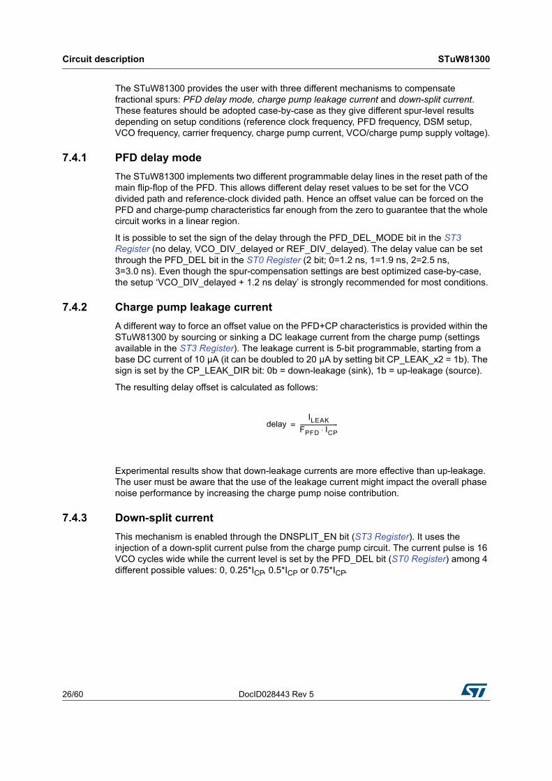
The PFD takes inputs from the reference and the VCO dividers and produces an output proportional to the phase error. The PFD includes a delay gate that controls the width of the anti-backlash pulse (1.2 to 3 ns). This pulse ensures that there is no dead zone in the PFD transfer function.
Figure 23 shows a simplified schematic of the PFD.
Figure 23. PFD diagram
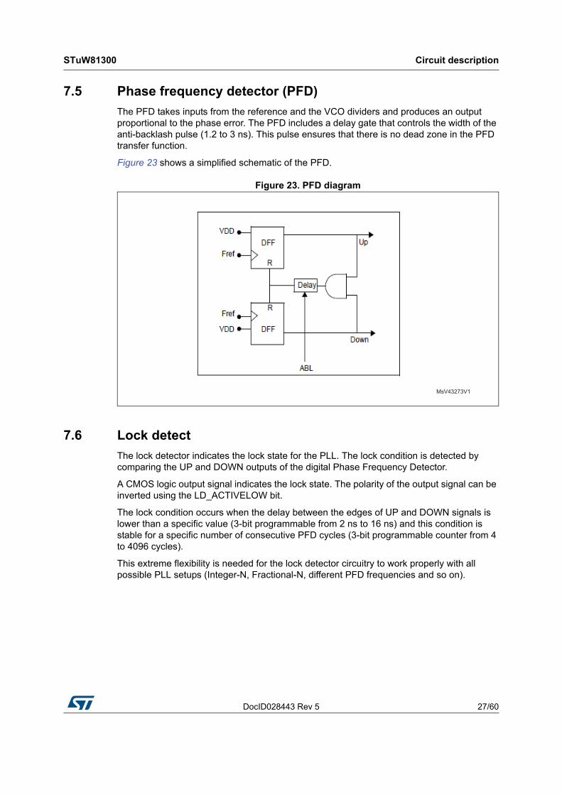
7.6 Lock detect
The lock detector indicates the lock state for the PLL. The lock condition is detected by comparing the UP and DOWN outputs of the digital Phase Frequency Detector.
A CMOS logic output signal indicates the lock state. The polarity of the output signal can be inverted using the LD_ACTIVELOW bit.
The lock condition occurs when the delay between the edges of UP and DOWN signals is lower than a specific value (3-bit programmable from 2 ns to 16 ns) and this condition is stable for a specific number of consecutive PFD cycles (3-bit programmable counter from 4 to 4096 cycles).
This extreme flexibility is needed for the lock detector circuitry to work properly with all possible PLL setups (Integer-N, Fractional-N, different PFD frequencies and so on).

Circuit description STuW81300
28/60 DocID028443 Rev 5
7.7 Charge pump
This block consists of two matched current sources, Iup and Idown, which are controlled respectively by the UP and DOWN PFD outputs. The nominal value of the output current (ICP) is controlled by selecting one of 32 values by a 5-bit word.
The minimum value of the output current (ICP) is 158 µA.
The charge pump also includes compensation circuitry to take into account variation of KVCO with VCO control voltage, which changes with temperature and process for a specified frequency. The KVCO compensation block adjusts the nominal ICP value, minimizing the variation of the product ICP x KVCO to keep the PLL bandwidth constant for the specified frequency. In order to compensate the change of KVCO with frequency, the user should manually adjust the ICP value to keep the PLL bandwidth constant.
In addition, the charge-pump output stage can operate with a 3.3 V to 4.5 V supply voltage. The LDO_4V5, programmable at 3.3 V and 4.5 V can be used for this purpose.
7.8 Fast lock mode
The fast-lock feature can be enabled to trade fast settling time against spurs rejection, performance parameters which generally require different settings of PLL bandwidth (narrow for better spurs rejection and wide for fast settling time).
A narrow bandwidth for low spurs can be designed for the lock state while a wide bandwidth can be designed for the PLL transients.
The wide bandwidth is achieved during the transient by increasing the charge pump current and reducing accordingly the dumping resistor value of the loop filter in order to keep the phase margin of the PLL constant. The duration of the PLL wide band mode, in terms of number of PFD cycles, is set by programming the fast-lock 13 bit counter.
Table 8. Current value vs. selection
CPSEL4 CPSEL3 CPSEL2 CPSEL1 CPSEL0 Current Value
0 0 0 0 0 - 0
0 0 0 0 1 IMIN 158 µA
0 0 0 1 0 3*IMIN 316 µA
... ... ... ... ... ... ...
1 1 1 0 1 29*IMIN 4.58 mA
1 1 1 1 0 30*IMIN 4.74 mA
1 1 1 1 1 31*IMIN 4.9 mA

DocID028443 Rev 5 29/60
STuW81300 Circuit description
56
7.9 Cycle slip reduction
The use of high FPFD/PLL_BW ratios may lead to an increased settling time due to cycle slips.
A cycle slip compensation circuit is provided which automatically increases the charge pump current for high-frequency errors and restores the programmed value at the end of the locking phase.
7.10 Voltage controlled oscillators (VCOs)
The STuW81300 employs four low-noise VCOs with monolithic LC tanks to cover a frequency range from 3850 MHz to 8000 MHz. Combined with an on-chip frequency doubler and divide-by-two stage, the VCOs allow synthesis of any frequency across the 1.925 GHz to 16 GHz range.
Each VCO is implemented using a structure with multiple sub-bands to maintain a low VCO sensitivity (KVCO), resulting in low phase-noise and low spurs performance.
The correct VCO and sub-band selection is automatically performed by dedicated digital circuitry (clocked by the PFD) every time a new frequency is programmed. The VCO auto-calibration procedure is activated once the ST0 Register is updated.
During the selection procedure the VCTRL of the VCO is charged to a fixed reference voltage.
The procedure for the VCO and sub-band selection takes approximately 13 * CALDIV PFD cycles, where CALDIV is the division ratio of the programmable divider included in the path between the PFD and the selection circuitry. The maximum frequency allowed for the sub-band selection is 250 kHz and the CALDIV value must be set accordingly if the PFD frequency is higher.
Once the correct VCO and sub-band are selected the normal PLL operations are resumed.
The VCO core can be supplied (pin#3) from 3.3 V to 4.5 V; the LDO_4V5 (programmable at 4.5 V and 3.3 V) is used for this purpose. Furthermore, the amplitude of oscillation, which trades current consumption with phase-noise performance is 3-bit programmable (ST4 Register, VCO_AMP bit). Section 7.16: STuW81300 register descriptions shows the allowed ranges of the oscillation amplitude for each available supply setting. In order to achieve the best phase-noise performance, the maximum allowed amplitude setting is recommended.
VCO calibration auto-restart feature
The VCO calibration auto-restart feature, once activated, allows the calibration procedure to be restarted when an event that moves the PLL into an unlock condition has occurred (trigger on ‘1’ to ‘0’ transition of the lock detector signal).
This feature can be enabled through the EN_AUTOCAL bit (ST6 Register) and requires proper setting of the lock detector parameters (LD_PREC and LD_COUNT, ST4 Register), in order to avoid any unwanted transition of the lock detector signal during the transient time required by the PLL to lock the VCO at the desired frequency.
Note: This feature is not available on product code STUW81300-1T, STUW81300-1TR.

Circuit description STuW81300
30/60 DocID028443 Rev 5
7.11 RF output stage
The VCO output signal can be fed either to an RF output buffer or to a monolithic frequency doubler, followed by a microwave output buffer.
The on-chip frequency multiplier allows the STuW81300 to cover a 7.7 GHz to 16 GHz frequency range with high fundamental harmonic rejection.
The STuW81300 employs two different 100-ohm differential (50-ohm single-ended) internally-matched broadband output stages, simplifying the design of the final application and reducing the number of external components.
A first RF output stage buffer (pins RF1_OUTP, RF1_OUTN) supports the 1925 MHz to 4000 MHz (using the divider-by-2 path) and 3850 MHz to 8000 MHz frequency ranges providing +6 dBm of output power @6 GHz into a 50-ohm single-ended resistive load.
The output stage buffer can be powered-down by software and/or hardware (pin PD_RF1).
A secondary microwave output stage (available on pins RF2_OUTP and RF2_OUTN) is also provided to deliver the VCO frequency-doubled signal (7.7 GHz-to-16 GHz) and is able to provide +4 dBm @12 GHz into a 50-ohm single-ended resistive load. This second output stage can also be powered down by software and/or hardware (pin PD_RF2).
An RF mute function, which allows RF output stages to be kept OFF until the PLL achieves lock status, can be selected by software.
The simultaneous use of both RF outputs (RF1 and RF2) is not supported. The user should configure the power down bit of the RF output stage so as to avoid enabling both RF outputs at the same time.

DocID028443 Rev 5 31/60
STuW81300 Circuit description
56
7.12 Low-power functional modes
All the performance characteristics defined in the electrical specifications are achieved in full current mode. The STuW81300 provides a set of low power functional modes to allow control of the current consumption of the different blocks.
This feature combined with the use of a 3.3 V regulated voltage for pins #3, 16, 32, can be helpful for applications requiring low power consumption. The power saving modes trade the current consumption with the phase-noise performance and/or output level.
7.13 LDO voltage regulators
Low drop-out (LDO) voltage regulators are integrated to provide the synthesizer with stable supply voltages against input voltage (VIN), load and temperature variations. Five regulators are included to ensure proper isolation among circuit blocks. These regulators are listed below along with the target specifications for the regulated output voltage (Vreg) and current capability:
• LDO_DIG (to supply the digital circuitry),
Vreg = 2.6 V, Imax = 50 mA, VIN range: 3.0 to 5.4 V
• LDO_PLL (to supply the PLL),
Vreg = 2.6 V, Imax = 50 mA, VIN range: 3.0 to 5.4 V
• LDO_RF (to supply the RF blocks),
Vreg = 2.6 V, Imax = 100 mA, VIN range: 3.0 to 5.4 V
• LDO_VCO (to supply the low-voltage VCO sub-blocks):
Vreg = 2.6 V, Imax = 100 mA, VIN range: 3.0 to 5.4 V
• LDO_4V5 (to supply high-voltage sub-blocks):
Vreg = 4.5 V and 3.3 V programmable, Imax = 150 mA
VIN range: 3.6 to 5.4 V (when Vreg = 3.3 V)
VIN range: 5.0 to 5.4 V (when Vreg=4.5 V)
Proper stability and frequency response are achieved by connecting 10 µF load capacitors at the regulated output pins. The optimal configuration is achieved by connecting a small resistor in series with the capacitor in order to guarantee the controlled ESR required to ensure the proper phase margin, together with the best performance in terms of noise and PSRR. For a complete view of required connections and component values associated with the LDO output pins, see the related PCB schematics section available from the STuW81300 product page on the ST website.
Very-low noise requirements have been assumed for the design of the VCO-related regulators (LDO_VCO and LDO_4V5). To comply with the noise specifications, these LDOs exploit an additional external bypass (feed forward) capacitor of 100 nF.
All LDOs include over-current protection to avoid short-circuit failures, as well as internal power ramping to minimize startup current peaks.
All LDOs operate from a reference voltage of 1.35 V, which is internally generated by an integrated band-gap circuit and noise-filtered through an external 10 µF capacitor.
Circuit description STuW81300
32/60 DocID028443 Rev 5
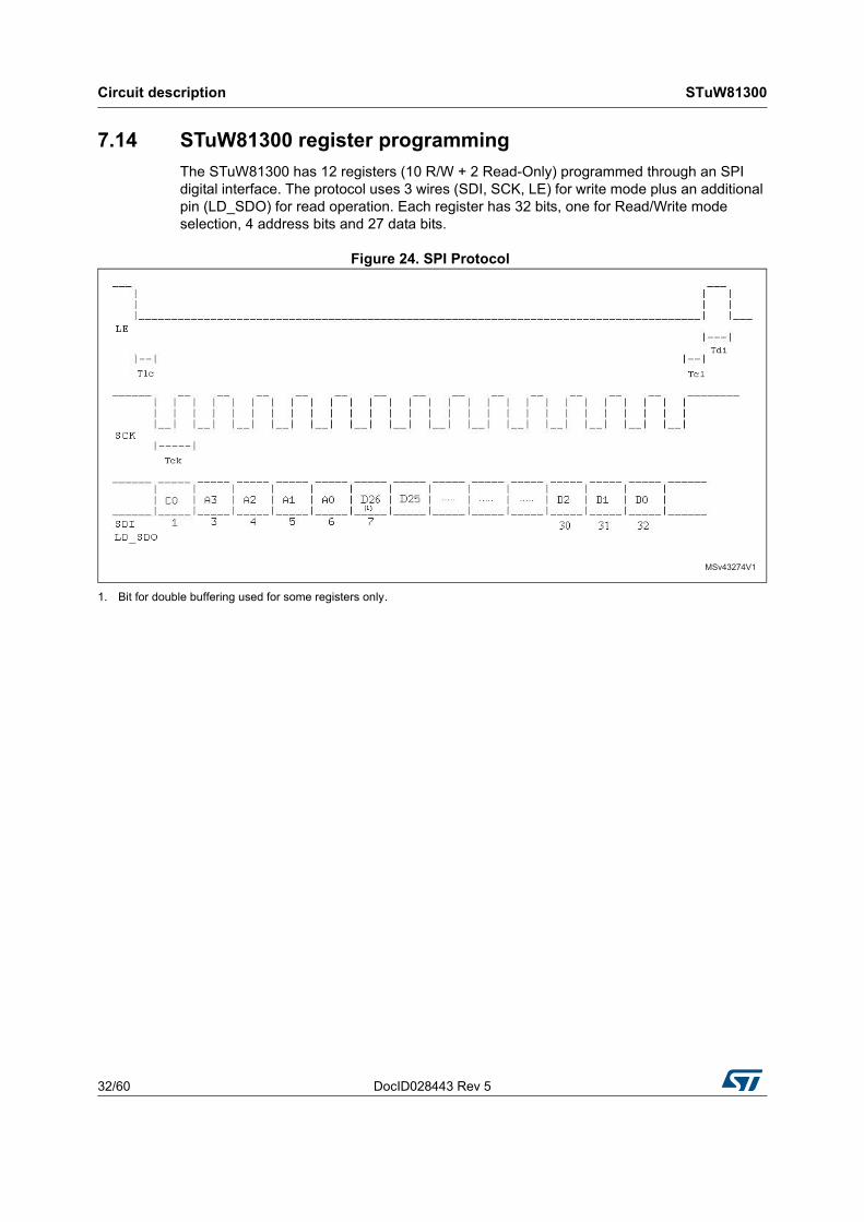
7.14 STuW81300 register programming
The STuW81300 has 12 registers (10 R/W + 2 Read-Only) programmed through an SPI digital interface. The protocol uses 3 wires (SDI, SCK, LE) for write mode plus an additional pin (LD_SDO) for read operation. Each register has 32 bits, one for Read/Write mode selection, 4 address bits and 27 data bits.
Figure 24. SPI Protocol
1. Bit for double buffering used for some registers only.

DocID028443 Rev 5 33/60
STuW81300 Circuit description
56
The Data bits are stored in the internal shift register on the rising edge of SCK.
The first bit, CO is used for mode selection (0=Write Operation, 1=Read Operation). The bits A[3:0] represent the register address, and D[26:0] are the data bits.
In some registers, the first data bit, D26, is used (when set to ‘1’) for double-buffering purposes. In this case the register content is stored in a temporary buffer and is transferred to the internal register once a write operation is done on the master register ST0.
Figure 25. SPI timing diagram
Table 9. SPI timings
Parameter Comments Min Typ Max Unit
Tsetup data to clock setup time 4 - - ns
Thold data to clock hold time 1 - - ns
Tck clock cycle period 20 - - ns
Tdi disable pulse width 4 - - ns
Tcd clock-to-disable time 1 - - ns
Tec enable-to-clock time 3 - - ns
Circuit description STuW81300
34/60 DocID028443 Rev 5
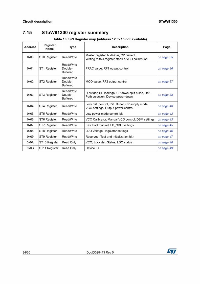
7.15 STuW81300 register summaryTable 10. SPI Register map (address 12 to 15 not available)
Address Register
NameType Description Page
0x00 ST0 Register Read/WriteMaster register. N divider, CP current. Writing to this register starts a VCO calibration
on page 35
0x01 ST1 RegisterRead/Write Double-Buffered
FRAC value, RF1 output control on page 36
0x02 ST2 RegisterRead/Write Double-Buffered
MOD value, RF2 output control on page 37
0x03 ST3 RegisterRead/Write Double-Buffered
R divider, CP leakage, CP down-split pulse, Ref. Path selection, Device power down
on page 38
0x04 ST4 Register Read/WriteLock det. control, Ref. Buffer, CP supply mode, VCO settings, Output power control
on page 40
0x05 ST5 Register Read/Write Low power mode control bit on page 42
0x06 ST6 Register Read/Write VCO Calibrator, Manual VCO control, DSM settings on page 43
0x07 ST7 Register Read/Write Fast Lock control, LD_SDO settings on page 45
0x08 ST8 Register Read/Write LDO Voltage Regulator settings on page 46
0x09 ST9 Register Read/Write Reserved (Test and Initialization bit) on page 47
0x0A ST10 Register Read Only VCO, Lock det. Status, LDO status on page 48
0x0B ST11 Register Read Only Device ID on page 49

DocID028443 Rev 5 35/60
STuW81300 Circuit description
56
7.16 STuW81300 register descriptions
ST0 Register
Address: STuW81300BaseAddress + 0x00
Type: R/W
Description: Master register. N divider, CP current
26 25 24 23 22 21 20 19 18 17 16 15 14 13 12 11 10 9 8 7 6 5 4 3 2 1 0
RE
SE
RV
ED
CP
_S
EL
[4
:0
]
PF
D_
DE
L[1
:0
]
RE
SE
RV
ED
RE
SE
RV
ED
N[1
6:0
]
W RW RW RW RW RW
[26] RESERVED: must be set to ‘0’ (Note: this bit is of type write-only and cannot be read. A read operation always returns '1')
[25:21] CP_SEL: set charge pump pulse current value (0 to 4.9 mA; step ~158 μA)
00000: (0) set ICP=0
00001: (1) set ICP=158 μA
00010: (2) set ICP=316 μA
…
11110: (30) set ICP=4.74 mA
11111: (31) set ICP=4.90 mA
[20:19] PFD_DEL: set PFD anti-backlash delay / down-split current value
00: (0) 1.2 ns / 0 A (default)
01: (1) 1.9 ns / 0.25*ICP
10: (2) 2.5 ns / 0.5*ICP
11: (3) 3.0 ns / 0.75*ICP
[18] RESERVED: must be set to ‘0’
[17] RESERVED: must be set to ‘0’
[16:0] N: Set integer part of N divider ratio (NINT)
For NINT ≥ 512, fractional mode is not allowed (FRAC and MOD settings are ignored)

Circuit description STuW81300
36/60 DocID028443 Rev 5
ST1 Register
Address: STuW81300BaseAddress + 0x01
Type: R/W
Applicability: Double buffered (based upon DBR bit setting)
Description: FRAC value, RF1 output control
26 25 24 23 22 21 20 19 18 17 16 15 14 13 12 11 10 9 8 7 6 5 4 3 2 1 0
DB
R
RE
SE
RV
ED
RF
1_
OU
T_
PD
MA
N_
CA
LB
_E
N
PL
L_
SE
L
RF
1_
SE
L
FR
AC
[2
0:0
]
RW RW RW RW RW RW RW
[26] DBR: double buffering bit enable
1: the register is buffered and transferred only once the master register ST0 is written
[25] RESERVED: must be set to ‘0’
[24] RF1_OUT_PD: RF1 output power down
0: RF1 output enabled
1: RF1 output disabled
[23] MAN_CALB_EN: enables manual VCO calibrator mode
0: automatic VCO calibration (VCO_SEL, VCO_WORD settings are ignored)
1: manual VCO calibration (VCO_SEL, VCO_WORD settings are used; VCO calibration procedure is inhibited; VCO_SEL and VCO_WORD bit to be set in ST6 Register)
[22] PLL_ SEL: selection of the signal path to PLL
0: VCO direct to PLL
1: VCO divided by 2 to PLL (mandatory for VCO freq > 6 GHz; in such a case the overall N value is doubled and NINT,FRAC and MOD must be updated accordingly at the half value)
[21] RF1_ SEL: RF1 output divider selection
0: VCO direct
1: VCO divided by 2
[20:0] FRAC: Fractional value bit; set the numerator value of the fractional part of the overall division ratio (N=NINT+FRAC/MOD)
Range: 0 to 2097151 (must be < MOD)

DocID028443 Rev 5 37/60
STuW81300 Circuit description
56
ST2 Register
Address: STuW81300BaseAddress + 0x02
Type: R/W
Applicability: Double buffered (based upon DBR bit setting)
Description: MOD value, RF2 output control
26 25 24 23 22 21 20 19 18 17 16 15 14 13 12 11 10 9 8 7 6 5 4 3 2 1 0
DB
R
DS
M_
CL
K_D
IS
AB
LE
RE
SE
RV
ED
RF
2_
OU
T_
PD
MO
D[2
0:0
]
RW RW RW RW RW
[26] DBR: Double buffering bit enable; at ‘1’ the register is buffered and transferred only once the master register ST0 is written
[25] DSM_CLK_DISABLE: for test purposes only. Must be set to ‘0’
[24:22] RESERVED: must be set to ‘0’
[21] RF2_OUT_PD: RF2 output power down
0: RF2 output enabled
1: RF2 output disabled (RF2 output must be disabled if RF1 output is enabled)
[20:0] MOD: Modulus value bit; set the denominator value of the fractional part of the overall division ratio (N=NINT+FRAC/MOD)
Range: 2 to 2097151
Circuit description STuW81300
38/60 DocID028443 Rev 5
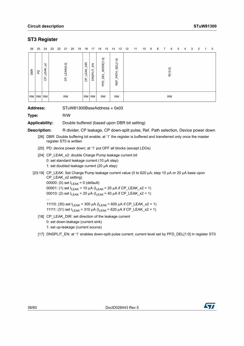
ST3 Register
Address: STuW81300BaseAddress + 0x03
Type: R/W
Applicability: Double buffered (based upon DBR bit setting)
Description: R divider, CP leakage, CP down-split pulse, Ref. Path selection, Device power down
26 25 24 23 22 21 20 19 18 17 16 15 14 13 12 11 10 9 8 7 6 5 4 3 2 1 0
DB
R
PD
CP
_LE
AK
_x2
CP
_L
EA
K[4
:0
]
CP
_L
EA
K_D
IR
DN
SP
LIT
_E
N
PF
D_
DE
L_
MO
DE
[1
:0]
RE
F_P
AT
H_
SE
L[1
:0
]
R[1
2:0]
RW RW RW RW RW RW RW RW RW
[26] DBR: Double buffering bit enable; at ‘1’ the register is buffered and transferred only once the master register ST0 is written
[25] PD: device power down; at ‘1’ put OFF all blocks (except LDOs)
[24] CP_LEAK_x2: double Charge Pump leakage current bit
0: set standard leakage current (10 µA step)
1: set doubled leakage current (20 µA step)
[23:19] CP_LEAK: Set Charge Pump leakage current value (0 to 620 μA; step 10 μA or 20 μA base upon CP_LEAK_x2 setting)
00000: (0) set ILEAK = 0 (default)
00001: (1) set ILEAK = 10 μA (ILEAK = 20 μA if CP_LEAK_x2 = 1)
00010: (2) set ILEAK = 20 μA (ILEAK = 40 μA if CP_LEAK_x2 = 1)
…
11110: (30) set ILEAK = 300 μA (ILEAK = 600 μA if CP_LEAK_x2 = 1)
11111: (31) set ILEAK = 310 μA (ILEAK = 620 μA if CP_LEAK_x2 = 1)
[18] CP_LEAK_DIR: set direction of the leakage current
0: set down-leakage (current sink)
1: set up-leakage (current source)
[17] DNSPLIT_EN: at ‘1’ enables down-split pulse current; current level set by PFD_DEL[1:0] in register ST0
DocID028443 Rev 5 39/60
STuW81300 Circuit description
56
[16:15] PFD_DEL_MODE: set PFD delay mode; delay values set by PFD_DEL[1:0] in register ST0
00: (0) no delay (default)
01: (1) VCO_DIV delayed
10: (2) REF_DIV delayed
11: (3) Reserved
[14:13] REF_PATH_SEL: reference clock path selection
00: (0) Direct
01: (1) Doubled in single mode; Not Applicable in differential mode
10: (2) Divided by 2
11: (3) Divided by 4
[12:0] R: set Reference clock divider ratio (1 to 8191)
Circuit description STuW81300
40/60 DocID028443 Rev 5
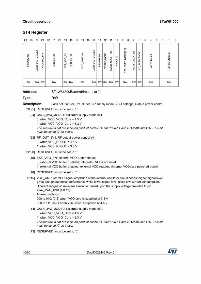
ST4 Register
Address: STuW81300BaseAddress + 0x04
Type: R/W
Description: Lock det. control, Ref. Buffer, CP supply mode, VCO settings, Output power control
26 25 24 23 22 21 20 19 18 17 16 15 14 13 12 11 10 9 8 7 6 5 4 3 2 1 0
RE
SE
RV
ED
CA
LB
_3
V3_
MO
DE
1
RF
_O
UT
_3V
3
RE
SE
RV
ED
EX
T_
VC
O_
EN
RE
SE
RV
ED
VC
O_
AM
P[2:0
]
CA
LB
_3
V3_
MO
DE
0
RE
SE
RV
ED
VC
AL
B_M
OD
E
KV
CO
_C
OM
P_D
IS
PF
D_
PO
L
RE
F_
BU
FF
_M
OD
E[1
:0
]
MU
TE
_L
OC
K_E
N
LD
_A
CT
IV
EL
OW
LD
_P
RE
C[2
:0]
LD
_C
OU
NT
[2
:0
]
RW RW RW RW RW RW RW RW RW RW RW RW RW RW RW RW RW
[26:25] RESERVED: must be set to ‘0’
[24] CALB_3V3_MODE1: calibrator supply mode bit1
0: when VCC_VCO_Core = 4.5 V
1: when VCC_VCO_Core = 3.3 V
This feature is not available on product codes STUW81300-1T and STUW81300-1TR. This bit must be set to ‘0’ on these.
[23] RF_OUT_3V3: RF output power control bit
0: when VCC_RFOUT = 4.5 V
1: when VCC_RFOUT = 3.3 V
[22:20] RESERVED: must be set to ‘0’
[19] EXT_VCO_EN: external VCO Buffer enable
0: external VCO buffer disabled; integrated VCOs are used
1: external VCO buffer enabled; external VCO required (internal VCOs are powered down)
[18] RESERVED: must be set to ‘0’
[17:15] VCO_AMP: set VCO signal amplitude at the internal oscillator circuit nodes; higher signal level gives best phase noise performance while lower signal level gives low current consumption.
Different ranges of value are available, based upon the supply voltage provided to pin VCC_VCO_core (pin #3).
Allowed settings:
000 to 010: (0-2) when VCO core is supplied at 3.3 V
000 to 111: (0-7) when VCO core is supplied at 4.5 V
[14] CALB_3V3_MODE0: calibrator supply mode bit0
0: when VCC_VCO_Core = 4.5 V
1: when VCC_VCO_Core = 3.3 V
This feature is not available on product codes STUW81300-1T and STUW81300-1TR. This bit must be set to ‘0’ on these.
[13] RESERVED: must be set to ‘0’
DocID028443 Rev 5 41/60
STuW81300 Circuit description
56
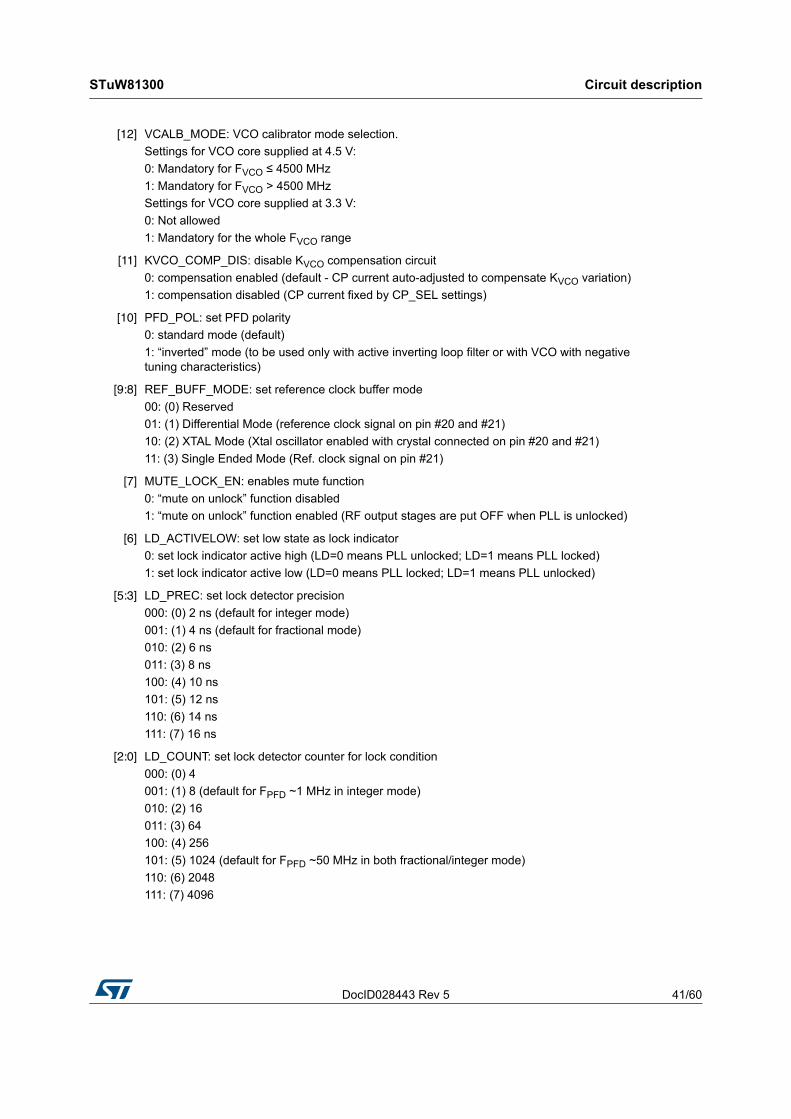
[12] VCALB_MODE: VCO calibrator mode selection.
Settings for VCO core supplied at 4.5 V:
0: Mandatory for FVCO ≤ 4500 MHz
1: Mandatory for FVCO > 4500 MHz
Settings for VCO core supplied at 3.3 V:
0: Not allowed
1: Mandatory for the whole FVCO range
[11] KVCO_COMP_DIS: disable KVCO compensation circuit
0: compensation enabled (default - CP current auto-adjusted to compensate KVCO variation)
1: compensation disabled (CP current fixed by CP_SEL settings)
[10] PFD_POL: set PFD polarity
0: standard mode (default)
1: “inverted” mode (to be used only with active inverting loop filter or with VCO with negative tuning characteristics)
[9:8] REF_BUFF_MODE: set reference clock buffer mode
00: (0) Reserved
01: (1) Differential Mode (reference clock signal on pin #20 and #21)
10: (2) XTAL Mode (Xtal oscillator enabled with crystal connected on pin #20 and #21)
11: (3) Single Ended Mode (Ref. clock signal on pin #21)
[7] MUTE_LOCK_EN: enables mute function
0: “mute on unlock” function disabled
1: “mute on unlock” function enabled (RF output stages are put OFF when PLL is unlocked)
[6] LD_ACTIVELOW: set low state as lock indicator
0: set lock indicator active high (LD=0 means PLL unlocked; LD=1 means PLL locked)
1: set lock indicator active low (LD=0 means PLL locked; LD=1 means PLL unlocked)
[5:3] LD_PREC: set lock detector precision
000: (0) 2 ns (default for integer mode)
001: (1) 4 ns (default for fractional mode)
010: (2) 6 ns
011: (3) 8 ns
100: (4) 10 ns
101: (5) 12 ns
110: (6) 14 ns
111: (7) 16 ns
[2:0] LD_COUNT: set lock detector counter for lock condition
000: (0) 4
001: (1) 8 (default for FPFD ~1 MHz in integer mode)
010: (2) 16
011: (3) 64
100: (4) 256
101: (5) 1024 (default for FPFD ~50 MHz in both fractional/integer mode)
110: (6) 2048
111: (7) 4096

Circuit description STuW81300
42/60 DocID028443 Rev 5
ST5 Register
Address: STuW81300BaseAddress + 0x05
Type: R/W
Description: Low power mode control bit
26 25 24 23 22 21 20 19 18 17 16 15 14 13 12 11 10 9 8 7 6 5 4 3 2 1 0
RE
SE
RV
ED
RF
2_
OU
TB
UF
_L
P
RE
SE
RV
ED
DE
MU
X_L
P
RE
SE
RV
ED
RE
F_
BU
FF
_L
P
RW RW RW RW RW RW
[26:5] RESERVED: must be set to ‘0’
[4] RF2_OUTBUF_LP: RF2 Output Buffer low power mode (0=full power; 1=low power)
[3] RESERVED: must be set to ‘0’
[2] DEMUX_LP: RF DEMUX low power mode (0=full power; 1=low power)
[1] RESERVED: must be set to ‘0’
[0] REF_BUFF_LP: reference buffer low power mode (0=full power; 1=low power)
DocID028443 Rev 5 43/60
STuW81300 Circuit description
56
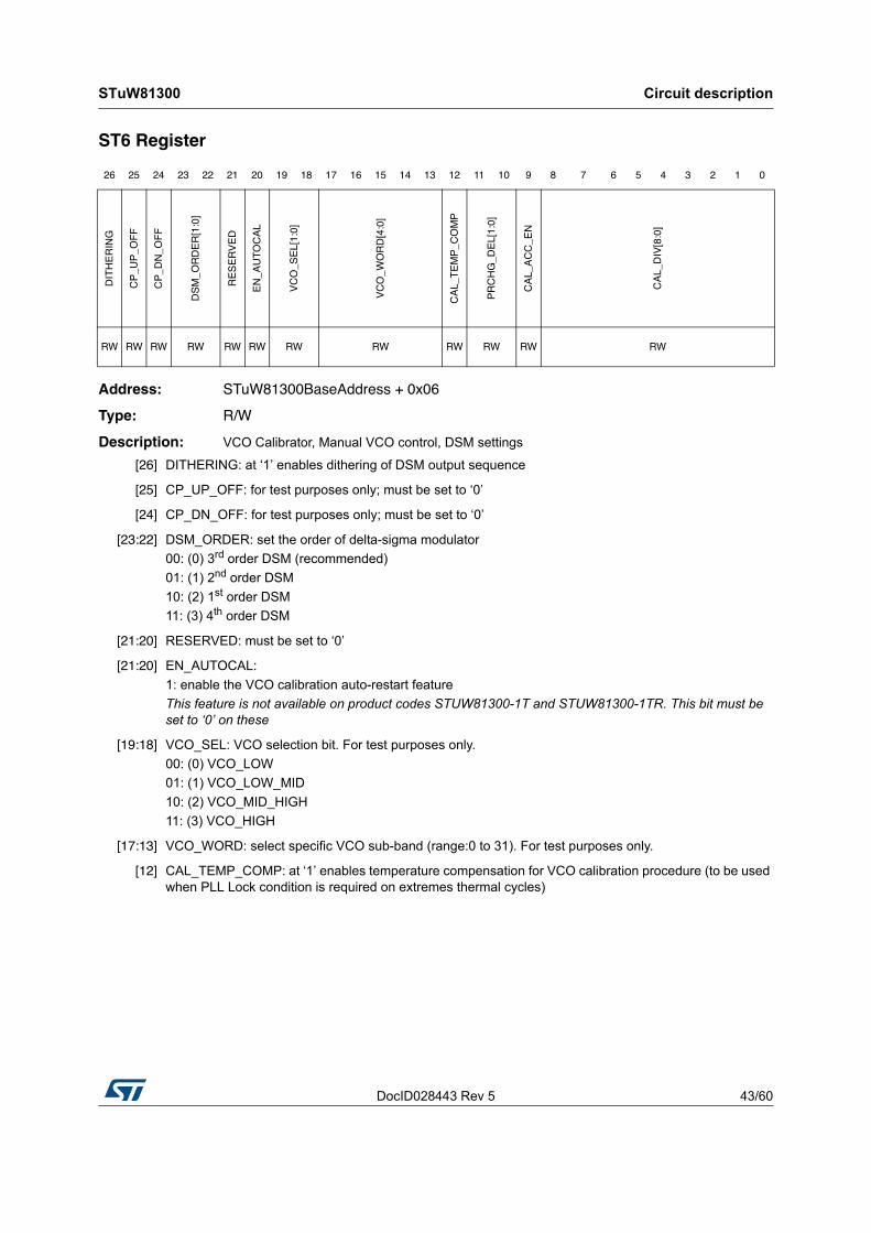
ST6 Register
Address: STuW81300BaseAddress + 0x06
Type: R/W
Description: VCO Calibrator, Manual VCO control, DSM settings
26 25 24 23 22 21 20 19 18 17 16 15 14 13 12 11 10 9 8 7 6 5 4 3 2 1 0
DIT
HE
RIN
G
CP
_U
P_
OF
F
CP
_D
N_
OF
F
DS
M_
OR
DE
R[1
:0
]
RE
SE
RV
ED
EN
_A
UT
OC
AL
VC
O_
SE
L[1:0
]
VC
O_
WO
RD
[4
:0
]
CA
L_
TE
MP
_C
OM
P
PR
CH
G_
DE
L[1
:0
]
CA
L_A
CC
_E
N
CA
L_
DIV
[8:0
]
RW RW RW RW RW RW RW RW RW RW RW RW
[26] DITHERING: at ‘1’ enables dithering of DSM output sequence
[25] CP_UP_OFF: for test purposes only; must be set to ‘0’
[24] CP_DN_OFF: for test purposes only; must be set to ‘0’
[23:22] DSM_ORDER: set the order of delta-sigma modulator
00: (0) 3rd order DSM (recommended)
01: (1) 2nd order DSM
10: (2) 1st order DSM
11: (3) 4th order DSM
[21:20] RESERVED: must be set to ‘0’
[21:20] EN_AUTOCAL:
1: enable the VCO calibration auto-restart feature
This feature is not available on product codes STUW81300-1T and STUW81300-1TR. This bit must be set to ‘0’ on these
[19:18] VCO_SEL: VCO selection bit. For test purposes only.
00: (0) VCO_LOW
01: (1) VCO_LOW_MID
10: (2) VCO_MID_HIGH
11: (3) VCO_HIGH
[17:13] VCO_WORD: select specific VCO sub-band (range:0 to 31). For test purposes only.
[12] CAL_TEMP_COMP: at ‘1’ enables temperature compensation for VCO calibration procedure (to be used when PLL Lock condition is required on extremes thermal cycles)

Circuit description STuW81300
44/60 DocID028443 Rev 5
[11:10] PRCHG_DEL: set the number of calibration slots for pre-charge of VCTRL node at the voltage reference value used during VCO calibration procedure
00: (0) 1 slot (default)
01: (1) 2 slots
10: (2) 3 slots
11: (3) 4 slots
[9] CAL_ACC_EN: at ‘1’ increase calibrator accuracy by removing residual error taking 2 additional calibration slots (default = ‘0’)
[8:0] CAL_DIV: Set Calibrator clock divider ratio (range:1 to 511); ‘0’ set the maximum ratio (‘511’)

DocID028443 Rev 5 45/60
STuW81300 Circuit description
56
ST7 Register
Address: STuW81300BaseAddress + 0x07
Type: R/W
Description: Fast Lock control, LD_SDO settings
26 25 24 23 22 21 20 19 18 17 16 15 14 13 12 11 10 9 8 7 6 5 4 3 2 1 0
RE
SE
RV
ED
LD
_S
DO
_tris
ta
te
LD
_S
DO
_M
OD
E
SP
I_D
ATA
_O
UT
_D
IS
AB
LE
LD
_S
DO
_S
EL
[1
:0
]
RE
GD
IG
_O
CP
_D
IS
CY
CL
E_
SL
IP
_E
N
FS
TL
CK
_E
N
CP
_S
EL
_F
L[4
:0
]
FS
TLC
K_
CN
T[12
:0]
RW RW RW RW RW RW RW RW RW RW
[26] RESERVED: must be set to ‘0’
[25] LD_SDO_tristate: at ‘1’ put LD_SDO out pin in tri-state mode
[24] LD_SDO_MODE: LD_SDO output interface mode selection
0: Open Drain mode (Level Range: 1.8V to 3.6V)
1: 2.5V CMOS output mode
[23] SPI_DATA_OUT_DISABLE: disable auto-switch of LD_SDO pin during SPI read mode
0: LD_SDO pin automatically switched to SPI data out line during SPI read mode
1: LD_SDO pin fixed to Lock detector indication (SPI read operation not possible)
[22:21] LD_SDO_SEL: LD_SDO multiplexer output selection bit
00: (0) Lock Detector (default)
01: (1) VCO Divider output (for test purposes only)
10: (2) Calibrator VCO Divider output (for test purposes only)
11: (3) Fast Lock clock output (for test purposes only)
[20] REGDIG_OCP_DIS: for test purposes only ; must be set to ‘0’ (at ‘1’ disable the over-current protection of Digital LDO Voltage Regulator)
[19] CYCLE_SLIP_EN: at ‘1’ enables cycle-slip feature
[18] FSTLCK_EN: at ‘1’ enables fast lock mode using pin #6 (PD_RF2/FL_SW)
[17:13] CP_SEL_FL: set the Charge Pump current during fast lock time slot (range:0 to 31)
[12:0] FSTLCK_CNT: Fast-Lock counter value (Range: 2 to 8191); set duration of fast-lock time slot as number of FPFD cycles

Circuit description STuW81300
46/60 DocID028443 Rev 5
ST8 Register
Address: STuW81300BaseAddress + 0x08
Type: R/W
Description: LDO Voltage Regulator settings
26 25 24 23 22 21 20 19 18 17 16 15 14 13 12 11 10 9 8 7 6 5 4 3 2 1 0
PD
_R
F2
_D
IS
AB
LE
RE
SE
RV
ED
RE
SE
RV
ED
RE
SE
RV
ED
RE
SE
RV
ED
RE
SE
RV
ED
RE
SE
RV
ED
RE
G_
OC
P_
DIS
RE
G_
DIG
_P
D
RE
G_D
IG
_V
OU
T[1
:0
]
RE
SE
RV
ED
RE
G_
RE
F_P
D
RE
G_R
EF
_V
OU
T[1
:0
]
RE
SE
RV
ED
RE
G_
RF
_P
D
RE
G_R
F_V
OU
T[1
:0
]
RE
SE
RV
ED
RE
G_
VC
O_
PD
RE
G_
VC
O_
VO
UT
[1
:0
]
RE
SE
RV
ED
RE
G_
VC
O_
4V
5_
PD
RE
G_
VC
O_
4V
5_
VO
UT
[1
:0
]
RW RW RW RW RW RW RW RW RW RW RW RW RW RW RW RW RW RW RW RW RW RW
[26] PD_RF2_DISABLE: at ‘1’ disable the hardware power down function of the pin PD_RF2 (pin #6) thus allowing the pin PD_RF1 (pin #5) to control the power down status of both RF output stages
[25] RESERVED: must be set to ‘0’
[24] RESERVED: must be set to ‘0’
[23] RESERVED: must be set to ‘0’
[22] RESERVED: must be set to ‘0’
[21] RESERVED: must be set to ‘0’
[20] RESERVED: must be set to ‘0’
[19] REG_OCP_DIS: for test purposes only; must be set to ‘0’ (at ‘1’ disable the over-current protection of LDO voltage regulators except DIG regulator)
[18] REG_DIG_PD: DIGITAL Regulator power down for test purposes only. Must be set to ‘0’
[17:16] REG_DIG_VOUT: DIGITAL regulator output voltage set
00: (0) 2.6 V (Default)
01: (1) 2.3 V (for test purposes only)
10: (2) 2.4 V (for test purposes only)
11: (3) 2.5 V (for test purposes only)
[15] RESERVED: must be set to ‘0’
[14] REG_REF_PD: REFERENCE CLOCK Regulator power down for test purposes only. Must be set to ‘0’
[13:12] REG_REF_VOUT: REFERENCE CLOCK Regulator output voltage set
00: (0) 2.6 V (default)
01: (1) 2.5 V (for test purposes only)
10: (2) 2.7 V (for test purposes only)
11: (3) 2.8 V (for test purposes only)
[11] RESERVED: must be set to ‘0’
[10] REG_RF_PD: RF Output section Regulator power down for test purposes only. Must be set to ‘0’

DocID028443 Rev 5 47/60
STuW81300 Circuit description
56
ST9 Register
Address: STuW81300BaseAddress + 0x09
Type: R/W
Description: Reserved (Test & Initialization bit)
[9:8] REG_RF_VOUT: RF output section regulator output voltage set
00: (0) 2.6 V (default)
01: (1) 2.5 V (for test purposes only)
10: (2) 2.7 V (for test purposes only)
11: (3) 2.8 V (for test purposes only)
[7] RESERVED: must be set to ‘0’
[6] REG_VCO_PD: VCO bias-and-control regulator power down for test purposes only. Must be set to ‘0’
[5:4] REG_VCO_VOUT: VCO bias-and-control regulator output voltage set
00: (0) 2.6 V (default)
01: (1) 2.5 V (for test purposes only)
10: (2) 2.7 V (for test purposes only)
11: (3) 2.8 V (for test purposes only)
[3] RESERVED: must be set to ‘0’
[2] REG_VCO_4V5_PD: High-voltage regulator power down (to be used to supply VCO core, RF output final stage and Charge Pump) for test purposes only. Must be set to ‘0’
[1:0] REG_VCO_4V5_VOUT: High-voltage regulator output voltage set (to be used to supply VCO core, RF output final stage and charge-pump output)
00: (0) 5.0 V (Requires 5.4 V unregulated voltage line on pin# 36, for test purposes only)
01: (1) 2.6 V (3.0 - 5.4 V unregulated voltage line range allowed on pin#36, for test purposes only)
10: (2) 3.3 V (3.6 - 5.4 V unregulated voltage line range allowed on pin#36)
11: (3) 4.5 V (5.0 - 5.4 V unregulated voltage line range allowed on pin#36)
26 25 24 23 22 21 20 19 18 17 16 15 14 13 12 11 10 9 8 7 6 5 4 3 2 1 0
RE
SE
RV
ED
RW
[26:0] RESERVED: Test and Initialization bit; must be set to ‘0’

Circuit description STuW81300
48/60 DocID028443 Rev 5
ST10 Register
Address: STuW81300BaseAddress + 0x0A
Type: R
Description: VCO, Lock det. Status, LDO status
26 25 24 23 22 21 20 19 18 17 16 15 14 13 12 11 10 9 8 7 6 5 4 3 2 1 0
RE
SE
RV
ED
RE
G_
DIG
_S
TA
RT
UP
RE
G_R
EF
_S
TA
RT
UP
RE
G_
RF
_S
TA
RT
UP
RE
G_
VC
O_
STA
RT
UP
RE
G_
VC
O_
4V
5_
STA
RT
UP
RE
G_D
IG
_O
CP
RE
G_
RE
F_
OC
P
RE
G_R
F_O
CP
RE
G_
VC
O_
OC
P
RE
G_
VC
O_
4V
5_
OC
P
LO
CK
_D
ET
VC
O_
SE
L[1:0
]
WO
RD
[4
:0]
R R R R R R R R R R R R R R
[26:18] RESERVED: fixed to ‘0’
[17] REG_DIG_STARTUP: DIGITAL regulator ramp-up indicator (‘1’ means correct start-up)
[16] REG_REF_STARTUP: REFERENCE CLOCK regulator ramp-up indicator (‘1’ means correct start-up)
[15] REG_RF_STARTUP: RF Output section regulator ramp-up indicator (‘1’ means correct start-up)
[14] REG_VCO_STARTUP: VCO bias-and-control regulator ramp-up indicator (‘1’ means correct start-up)
[13] REG_VCO_4V5_STARTUP: High-voltage regulator ramp-up indicator (‘1’ means correct start-up)
[12] REG_DIG_OCP: DIGITAL regulator over-current protection indicator (‘1’ means over-current detected)
[11] REG_REF_OCP: REFERENCE CLOCK regulator over-current protection indicator (‘1’ means over-current detected)
[10] REG_RF_OCP: RF Output section regulator over-current protection indicator (‘1’ means over-current detected)
[9] REG_VCO_OCP: VCO bias and control regulator over-current protection indicator (‘1’ means over-current detected)
[8] REG_VCO_4V5_OCP: high-voltage regulator over-current protection indicator (‘1’ means over-current detected)
[7] LOCK_DET: Lock detector status bit (‘1’ means PLL locked)
[6:5] VCO_SEL: VCO selected by calibration algorithm
00: (0) VCO_LOW
01: (1) VCO_LOW_MID
10: (2) VCO_MID_HIGH
11: (3) VCO_HIGH
[4:0] WORD: specific VCO sub-band selected by calibration algorithm (range:0 to 31)

DocID028443 Rev 5 49/60
STuW81300 Circuit description
56
ST11 Register
Address: STuW81300BaseAddress + 0x0B
Type: R
Description: Device identifier
26 25 24 23 22 21 20 19 18 17 16 15 14 13 12 11 10 9 8 7 6 5 4 3 2 1 0
Dev
ice
_ID
R
[26:0] Device_ID:
0x000804B for product codes STUW81300-1T and STUW81300-1TR
0x0008052 for product codes STUW81300T and STUW81300TR

Circuit description STuW81300
50/60 DocID028443 Rev 5
7.17 Power-on sequence
In order to guarantee the correct start-up of the internal circuitry after the power on, the following steps must be followed:
1. Power up the device (LDO supply pins: pin#9 #18, #28 and #36)
2. Once the voltages applied on the LDO supply pins are stable, wait 50 ms. (After this transient time, the LDOs are powered on with the regulated voltages available at pins #2, #8, #19, #27 and #29, while all other circuits are in power down mode).
3. Provide the reference clock signal.
4. Implement the first programming sequence as follows:
a) program register ST9 (test and initialization) with all bits set to ‘0’.
b) program register ST0 according to the desired configuration
c) program the following registers in the specified order according to the desired configuration: ST8, ST7, ST6, ST5, ST4, ST3, ST2, ST1, ST0.
5. Check the PLL Lock status on pin LD_SDO (pin #26) and/or read all relevant information provided on registers ST10 and ST11.
7.18 Example register programming
Setup conditions and requirements
• Unregulated Supply voltage: 5.0 V
• Reference Clock: 100 MHz , single-ended, sine wave
• LO Frequency: 15220 MHz – exact freq. mode (VCO Frequency=7610 MHz)
• Phase Noise requirements: full performance VCO; full performance Noise floor
Register configurations (Hex values including register address)
• ST9 = 0x48000000 (initialization; all bits set to ‘0’)
• ST8 = 0x40000003 (REG_4V5 = 4.5 V)
• ST7 = 0x39000000 (“fast lock” not used; LD_SDO pin configured as 2.5 V CMOS buffer)
• ST6 = 0x30001000 (DITHERING=0; DSM_ORDER=0 for 3rd order DSM; CAL_TEMP_COMP = 1 to keep lock over temperature drift; CALDIV = 0)
• ST5 = 0x28000000 (low power modes not used)
• ST4 = 0x20039315 (lock detector setting for fractional mode and FPFD = 50 MHz; REF_BUF_MODE=3 for single-ended mode; VCO_AMP = 7 for best VCO phase noise @4.5 V supply; VCALB_MODE=1 for VCO frequency>4500 MHz)
• ST3 = 0x18008002 (PFD_DEL_MODE = ”VCO_DIV_delayed”; R=2 and REF_PATH_SEL=0 “direct” for FPFD = 50 MHz)
• ST2 = 0x1000000A (MOD=10; RF2_OUT_PD = 0 for RF2 output with VCO doubled frequency)
• ST1 = 0x09400001 (FRAC = 1 RF2_OUT_PD = 1 set RF1 output in power down; PLL_SEL = 1 to enable VCO divider by 2 path to PLL as VCO freq > 6 GHz)
• ST0 = 0x03E0004C (NINT = 76; PFD_DEL = 1.2 ns; CPSEL = 31 for ICP = 4.9 mA)
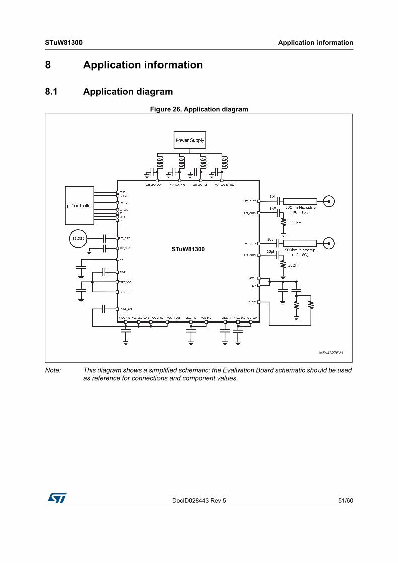
DocID028443 Rev 5 51/60
STuW81300 Application information
56
8 Application information
8.1 Application diagram
Figure 26. Application diagram
Note: This diagram shows a simplified schematic; the Evaluation Board schematic should be used as reference for connections and component values.
STuW81300

Application information STuW81300
52/60 DocID028443 Rev 5
8.2 Thermal PCB design considerations
The STuW81300 QFN package offers a low thermal resistance (θJC ~3 °C/W on a JEDEC Multi-Layer Board). Preferred thermal flow in QFN package is through the bottom central pad.
The central thermal pad provides a solderable surface on the top of the PCB (for soldering the package die paddle on the board). Thermal vias are needed to provide a thermal path to the inner and bottom layers of the PCB in order to remove/dissipate the heat. The size of the thermal pad can be matched with the exposed die paddle, or it may be smaller taking into consideration clearance for vias to route the inner row signals.
A PCB can be designed to achieve a thermal impedance of 2 to 4 °C/W through a 1.6 mm (.063”) thick FR-4 type PCB (a reliable, low cost solution).
For example the ST EVAL KIT uses a 0.8 mm thick PCB with a thermal impedance of ~50 °C/W for a single via filled with solder. 25 vias are used, giving a thermal impedance of ~2 °C/W with solder-filled vias (50 °C/W divided by 25 vias).
Using a plate on the underside of the PCB (a common solution in STuW81300 applications, as the plate is typically the metal housing of the application assembly) brings the total thermal resistance (junction to housing in the customer application) below 10 °C/W.
As the typical power dissipation of the STuW81300 is approximately 1.5 W, at maximum specified ambient temperature (85 °C) a junction temperature of ~100 °C is attainable. This is well below the maximum specified value (125 °C) to ensure safe operation of the STuW81300 in worst-temperature conditions.
The ST EVAL KIT is not provided with additional heatsinking, and the thermal resistance (θJA) measured in the EVAL BOARD is ~30 °C/W.
8.3 Robust VCO calibration over full temperature range
Some applications require synthesis of a fixed frequency while keeping the lock condition, without any phase/frequency jumps, even if temperature drift occurs over the whole operating temperature range.
In such cases, the capability of the STuW81300 to stay locked - with the specific VCO and sub-bands selected by the VCO auto-calibration procedure - is defined by the ΔTLOCK parameter (see Table 6: Electrical specifications).
If the application requires a larger temperature drift, a factory VCO calibration at fixed/controlled temperature may be applied.
The concept is to run the standard VCO auto-calibration procedure (after writing the ST0 Register) in the factory at 25 °C. The resulting frequency, VCO and sub-band information is then stored in non-volatile memory. In the field, the STuW81300 is set up using a manual VCO calibration, recalling the VCO and sub-band data previously stored in the application memory.
In this way, with a good thermal PCB design to limit the maximum junction temperature to 100 °C (see Section 8.2: Thermal PCB design considerations), the STuW81300 VCO is calibrated virtually at 25 °C, regardless of the effective temperature during in-field setup. This guarantees the lock condition for any temperature drift within the operating temperature range.
DocID028443 Rev 5 53/60
STuW81300 Application information
56
In order to execute the robust VCO calibration in-factory at a controlled temperature (25 °C), a software routine must be implemented that is able to:
• Program the device over the desired VCO frequency range (5 MHz frequency step or lower, regardless of the application frequency step)
• Read the lock detector indication (from the LD_SDO pin or from the ST10 Register)
• Read the VCO_SEL (2 bits) and WORD (5 bits) from the ST10 Register
• Store the data (VCO frequency, VCO_SEL and WORD) in the non-volatile memory of the application.
The procedure is detailed below, using an example where the application requires synthesis of a carrier frequency over a wide range; from 11.8 GHz to 12.2 GHz. Hence the VCO should be pre-calibrated in-factory over the frequency range 5.9 GHz to 6.1 GHz.
1. Execute the power-up procedure (see Section 7.17: Power-on sequence) configuring the device registers (see Section 7.18: Example register programming) with suitable settings for the first VCO frequency (5.9 GHz):
a) Wait for the lock time, read the lock detector, read VCO_SEL and WORD from the ST10 Register
b) Store frequency data (5.9 GHz), VCO_SEL and WORD values in memory.
2. Configure the device for the next VCO frequency (5.905 GHz):
a) Wait for the lock time, read the lock detector, read VCO_SEL and WORD values from the ST10 Register.
b) Store frequency data, VCO_SEL and WORD values in memory only if the current values of the pair VCO_SEL/WORD are different from the previous step.
3. Configure the device for next VCO frequency (5.91 GHz):
a) Repeat step 2 a)
b) Repeat step 2 b)
Next steps. Repeat step 3 for all intermediate frequencies (5.915, 5.92,.. 6.095 GHz).
Final step. Configure the device for the last VCO frequency (6.1 GHz):
a) Wait for the lock time, read the lock detector, read VCO_SEL and WORD values from the ST10 Register.
b) Store frequency data, VCO_SEL and WORD values in memory only if the current values of the pair VCO_SEL/WORD are different from the previous step.
Note: The number of records to be stored in memory is less than the number of steps performed, requiring only a small amount of memory. In our example we have swept 41 VCO frequency steps but only 7 records need to be saved (the number of records to be stored depends on the VCO sub-band spacing).

Application information STuW81300
54/60 DocID028443 Rev 5
The operations to be performed in-field in order to configure the device at VCO frequency = 6.0 GHz are:
1. Execute the power-up procedure, configuring the device registers with suitable settings for the desired VCO frequency (6.0 GHz), with VCO auto-calibration disabled (see step 2 below)
2. Write registers as indicated in Section 7.18: Example register programming, setting the MAN_CALB_EN bit (ST1 Register ) to ‘1’. Use the pair VCO_SEL/WORD stored in the memory (2/25 from record number 4 for 6.0 GHz) to set the VCO_SEL and VCO_WORD bits (ST6 Register).
The count of the records and the values of stored VCO_SEL/WORD pairs changes slightly when applying the same routine over different samples, so this calibration procedure is needed for each part.
Table 11. Example of data for robust VCO calibration routine to be stored in the application memory
VCO frequency (MHz) VCO_SEL WORD Notes
5900 1 1 Range (5900 to 5914.999 MHz) uses VCO=1, WORD=1
5915 1 0 Range (5915 to 5964.999 MHz) uses VCO=1, WORD=0
5965 2 26 Range (5965 to 5979.999 MHz) uses VCO=2, WORD=26
5980 2 25 Range (5980 to 6009.999 MHz) uses VCO=2, WORD=25
6010 2 24 Range (6010 to 6044.999 MHz) uses VCO=2, WORD=24
6045 2 23 Range (6045 to 6079.999 MHz) uses VCO=2, WORD=23
6080 2 22 Range (6080 to 6100 MHz) uses VCO=2, WORD=22
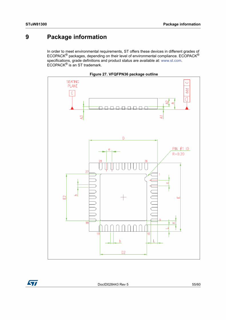
DocID028443 Rev 5 55/60
STuW81300 Package information
56
9 Package information
In order to meet environmental requirements, ST offers these devices in different grades of ECOPACK® packages, depending on their level of environmental compliance. ECOPACK® specifications, grade definitions and product status are available at: www.st.com. ECOPACK® is an ST trademark.
Figure 27. VFQFPN36 package outline

Package information STuW81300
56/60 DocID028443 Rev 5
1. VFQFNP stands for Thermally Enhanced Very thin Fine pitch Quad Flat Package No lead. Very thin: A=1.00 Max.
2. Details of terminal 1 identifier are optional but must be located on the top surface of the package by using either a mold or marked features.
Table 12. VFQFPN36 package mechanical data
REF. MIN. TYP. MAX. NOTES
A 0.80 0.90 1.00 -
A1 - 0.02 0.05 -
A2 - 0.65 1.00 -
A3 - 0.20 - -
b 0.18 0.23 0.30 -
D 5.875 6.00 6.125 -
D2 4.15 4.30 4.45 -
E 5.875 6.00 6.125 -
E2 4.15 4.30 4.45 -
e 0.45 0.50 0.55 -
L 0.35 0.55 0.75 -
K 0.25 - - -
ddd - - 0.08 -

DocID028443 Rev 5 57/60
STuW81300 Evaluation kit
57
10 Evaluation kit
An evaluation kit can be delivered upon request (see Table 13 for order codes), including the following items:
• Evaluation board
• GUI (graphical user interface) to configure the board and the STuW81300 IC
• STWPLLSim software for PLL loop filter design and phase noise/transient simulation
• A comprehensive set of documentation (evaluation-board data brief including PCB schematics, GUI help and STWPLLSim user manual).
The evaluation kit and related software and documentation can be ordered/downloaded at www.st.com.
Table 13. STuW81300 evaluation-kit order codes
Order Code Description
STuW81300-EVB STuW81300 Evaluation Kit (evaluation board, GUI and STWPLLSim tool)
STSW-RFSOL001 STWPLLSim simulation tool for STuW81300
STSW-RFSOL003 GUI for configuring STuW81300 evaluation board
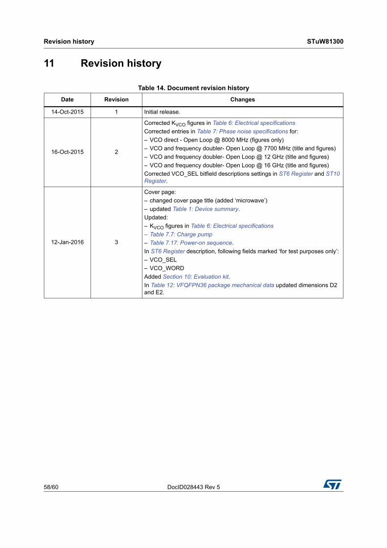
Revision history STuW81300
58/60 DocID028443 Rev 5
11 Revision history
Table 14. Document revision history
Date Revision Changes
14-Oct-2015 1 Initial release.
16-Oct-2015 2
Corrected KVCO figures in Table 6: Electrical specifications
Corrected entries in Table 7: Phase noise specifications for:
– VCO direct - Open Loop @ 8000 MHz (figures only)
– VCO and frequency doubler- Open Loop @ 7700 MHz (title and figures)
– VCO and frequency doubler- Open Loop @ 12 GHz (title and figures)
– VCO and frequency doubler- Open Loop @ 16 GHz (title and figures)
Corrected VCO_SEL bitfield descriptions settings in ST6 Register and ST10 Register.
12-Jan-2016 3
Cover page:
– changed cover page title (added ‘microwave’)
– updated Table 1: Device summary.
Updated:
– KVCO figures in Table 6: Electrical specifications
– Table 7.7: Charge pump
– Table 7.17: Power-on sequence.
In ST6 Register description, following fields marked ‘for test purposes only’:
– VCO_SEL
– VCO_WORD
Added Section 10: Evaluation kit.
In Table 12: VFQFPN36 package mechanical data updated dimensions D2 and E2.

DocID028443 Rev 5 59/60
STuW81300 Revision history
59
12-Aug-2016 4
Explicitly defined supply connections in: Table 2: Pin descriptions.
Updated VCC parameter in:
– Table 3: Absolute maximum ratings
– Table 4: Operating conditions.
Removed block-specific power supply parameters and TLK definition from
Table 6: Electrical specifications.
Aligned supply range to 4.5 V max. in:
– Table 7: Phase noise specifications
– Section 7.7: Charge pump (also removed register dependence)
– Section 7.10: Voltage controlled oscillators (VCOs).
Updated: Section 7.13: LDO voltage regulators
In ST0 Register updated type and description of bit 26.
In ST3 Register corrected width of bitfield R[12:0].
In ST4 Register updated:
– width and description of bitfield VCO_AMP[2:0])
– description of bitfield CP_SUPPLY_MODE.
In ST8 Register updated descriptions of bitfields:
– REG_DIG_PD
– REG_REF_PD
– REG_RF_PD.
Updated Section 7.18: Example register programming.
Updated Table 12: VFQFPN36 package mechanical data.
16-Dec-2016 5
Changed document settings to ‘production data’.
Updated Table 1: Device summary.
Added ΔTLOCK parameters in Table 6: Electrical specifications, including:
– VCC_VCO_Core = 3.3 V ΔTLOCK operation (product code exclusions mentioned in table footnote)
– ΔTLOCK operation at VCC_VCO_Core = 4.5 V indicated.
In Table 7: Phase noise specifications specified:
– VCO direct – open loop @ 6 GHz, VCC_VCO_Core = 3.3 V
– VCO and frequency doubler – open loop @ 12 GHz, VCC_VCO_Core = 3.3 V
– Added VCC_VCO_Core conditions for all other parameters.
Updated Section 7.1: Reference input stage.
Updated Section 7.10: Voltage controlled oscillators (VCOs)
Added VCO calibration auto-restart feature on page 29.
In ST4 Register:
– Replaced bitfield CP_SUPPLY_MODE with VCALB_MODE
– Added bitfields CALB_3V3_MODE0 and CALB_3V3_MODE1.
Removed bitfield DOUBLER_LP in ST5 Register.
Added bitfield EN_AUTOCAL in ST6 Register.
Updated device identifier in ST11 Register.
Updated Register configurations (Hex values including register address) on page 50.
Added new Section 8.3: Robust VCO calibration over full temperature range.
Table 14. Document revision history
Date Revision Changes

STuW81300
60/60 DocID028443 Rev 5
IMPORTANT NOTICE – PLEASE READ CAREFULLY
STMicroelectronics NV and its subsidiaries (“ST”) reserve the right to make changes, corrections, enhancements, modifications, and improvements to ST products and/or to this document at any time without notice. Purchasers should obtain the latest relevant information on ST products before placing orders. ST products are sold pursuant to ST’s terms and conditions of sale in place at the time of order acknowledgement.
Purchasers are solely responsible for the choice, selection, and use of ST products and ST assumes no liability for application assistance or the design of Purchasers’ products.
No license, express or implied, to any intellectual property right is granted by ST herein.
Resale of ST products with provisions different from the information set forth herein shall void any warranty granted by ST for such product.
ST and the ST logo are trademarks of ST. All other product or service names are the property of their respective owners.
Information in this document supersedes and replaces information previously supplied in any prior versions of this document.
© 2016 STMicroelectronics – All rights reserved
Related Documents