www.infineon.com Please note that Cypress is an Infineon Technologies Company. The document following this cover page is marked as “Cypress” document as this is the company that originally developed the product. Please note that Infineon will continue to offer the product to new and existing customers as part of the Infineon product portfolio. Continuity of document content The fact that Infineon offers the following product as part of the Infineon product portfolio does not lead to any changes to this document. Future revisions will occur when appropriate, and any changes will be set out on the document history page. Continuity of ordering part numbers Infineon continues to support existing part numbers. Please continue to use the ordering part numbers listed in the datasheet for ordering.

Welcome message from author
This document is posted to help you gain knowledge. Please leave a comment to let me know what you think about it! Share it to your friends and learn new things together.
Transcript

www.infineon.com
Please note that Cypress is an Infineon Technologies Company.The document following this cover page is marked as “Cypress” document as this is the company that originally developed the product. Please note that Infineon will continue to offer the product to new and existing customers as part of the Infineon product portfolio.
Continuity of document contentThe fact that Infineon offers the following product as part of the Infineon product portfolio does not lead to any changes to this document. Future revisions will occur when appropriate, and any changes will be set out on the document history page.
Continuity of ordering part numbersInfineon continues to support existing part numbers. Please continue to use the ordering part numbers listed in the datasheet for ordering.
www.cypress.com Document No. 001-72419 Rev. *C 1
AN72419
West Bridge® Benicia™ Hardware Design Guidelines and Schematic Checklist
Author: Rizwan Afridi, Hussein Osman
Associated Project: No
Associated Part Family: CYWB0263BB
Software Version: N/A
Related Application Notes: None
AN72419 discusses the hardware design best practices and the device configuration for the West Bridge® Benicia™
device. The application note provides effective system design and PCB layout techniques to jumpstart your project.
Contents
1 Introduction ............................................................... 1 2 Power System .......................................................... 2
2.1 Overview .......................................................... 2 2.2 Power Supply Configuration ............................ 2 2.3 Power Modes ................................................... 3 2.4 Device Supply Decoupling ............................... 4 2.5 Inrush Current Consideration and
Power Supply Design .......................................... 4 3 Clocking .................................................................... 7
3.1 Crystal.............................................................. 7 3.2 Clock ................................................................ 8 3.3 Frequency Select ............................................. 9 3.4 Watchdog Timer .............................................. 9
4 P-port Interface ......................................................... 9
5 S-port Interface ....................................................... 10 6 Low Performance Peripherals (LPP) ...................... 11
6.1 I2C Interface ................................................... 11 6.2 JTAG ............................................................. 12 6.3 I2S .................................................................. 12 6.4 SPI and UART ............................................... 12
7 Booting ................................................................... 12 8 EMI and ESD Considerations ................................. 13 9 Benicia Device Package Dimensions ..................... 14 10 Electrical Design Consideration .............................. 14
10.1 USB 3.0 SuperSpeed Design Guidelines ...... 14 Document History ............................................................ 24 Worldwide Sales and Design Support ............................. 25
1 Introduction
West Bridge Benicia is a USB 3.0 SuperSpeed peripheral controller optimized for sideloading and streaming applications. West Bridge Benicia supports the latest removable and embedded mass-storage devices such as SD 3.0 (SDXC with UHS-I) and eMMC 4.41. It also boosts the USB data rate from 480 Mbps (High Speed) to 5 Gbps (SuperSpeed).
To successfully integrate this high-performance peripheral in a system, the designer should consider the provided configuration and layout recommendation and ensure correct system operation.
This application note provides schematic and layout design guidelines for designs using Cypress Benicia device. For datasheet of the device please contact Cypress technical support (www.cypress.com > Design Support > Create a Customer Case).
West Bridge® Benicia™ Hardware Design Guidelines
www.cypress.com Document No. 001-72419 Rev. *C 2
2 Power System
2.1 Overview
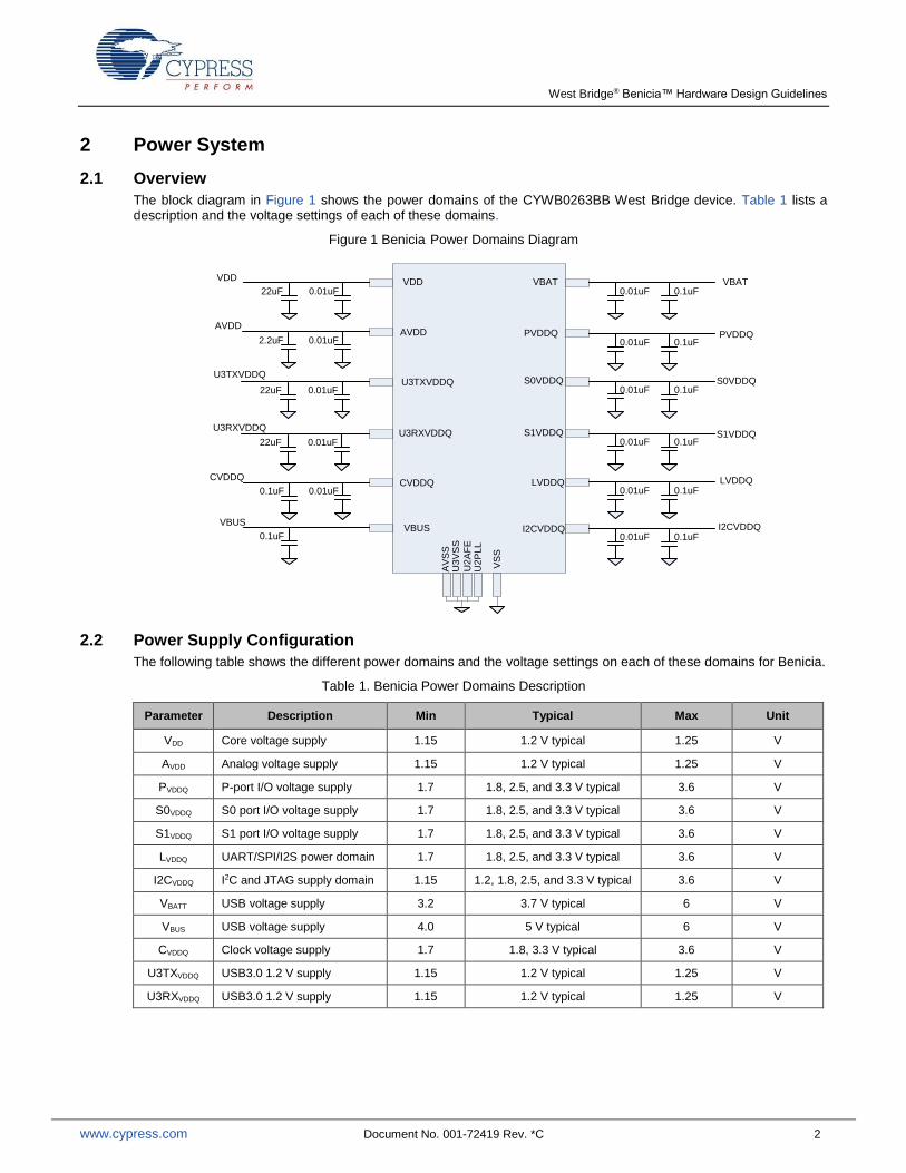
The block diagram in Figure 1 shows the power domains of the CYWB0263BB West Bridge device. Table 1 lists a description and the voltage settings of each of these domains.
Figure 1 Benicia Power Domains Diagram
VBAT
PVDDQ
S0VDDQ
S1VDDQ
LVDDQ
I2CVDDQ
VDD
U3RXVDDQ
VBAT0.01uF 0.1uF
PVDDQ0.01uF 0.1uF
S0VDDQ0.01uF 0.1uF
S1VDDQ0.01uF 0.1uF
LVDDQ0.01uF 0.1uF
I2CVDDQ0.01uF 0.1uF
CVDDQ
AVDD
U3TXVDDQ
VBUS
VDD
0.01uF22uF
U3RXVDDQ
0.01uF22uF
CVDDQ
0.01uF0.1uF
AVDD
0.01uF2.2uF
U3TXVDDQ
0.01uF22uF
0.1uF
VS
S
AV
SS
U2
AF
E
U3
VS
S
U2
PL
L
VBUS
2.2 Power Supply Configuration
The following table shows the different power domains and the voltage settings on each of these domains for Benicia.
Table 1. Benicia Power Domains Description
Parameter Description Min Typical Max Unit
VDD Core voltage supply 1.15 1.2 V typical 1.25 V
AVDD Analog voltage supply 1.15 1.2 V typical 1.25 V
PVDDQ P-port I/O voltage supply 1.7 1.8, 2.5, and 3.3 V typical 3.6 V
S0VDDQ S0 port I/O voltage supply 1.7 1.8, 2.5, and 3.3 V typical 3.6 V
S1VDDQ S1 port I/O voltage supply 1.7 1.8, 2.5, and 3.3 V typical 3.6 V
LVDDQ UART/SPI/I2S power domain 1.7 1.8, 2.5, and 3.3 V typical 3.6 V
I2CVDDQ I2C and JTAG supply domain 1.15 1.2, 1.8, 2.5, and 3.3 V typical 3.6 V
VBATT USB voltage supply 3.2 3.7 V typical 6 V
VBUS USB voltage supply 4.0 5 V typical 6 V
CVDDQ Clock voltage supply 1.7 1.8, 3.3 V typical 3.6 V
U3TXVDDQ USB3.0 1.2 V supply 1.15 1.2 V typical 1.25 V
U3RXVDDQ USB3.0 1.2 V supply 1.15 1.2 V typical 1.25 V

West Bridge® Benicia™ Hardware Design Guidelines
www.cypress.com Document No. 001-72419 Rev. *C 3
2.3 Power Modes
West Bridge Benicia supports the following power modes:
Normal mode: This is the full functional operating mode. In this mode, the internal CPU clock and the internal PLLs are enabled.
The I/O power supplies S0VDDQ, S1VDDQ, LVDDQ, and I2CVDDQ may be turned off when the corresponding interface is not in use. PVDD may not be turned off at any time if the P-port interface is used in the application.
The USB I/O requires a 3.3-V regulated power supply. This supply is internally driven from either the VBUS or VBATT external supplies. VBATT/VBUS can be turned off if USB is not used. If the USB port is used, one or both supplies must be present.
VBATT can be connected to the system battery or a stable 3.2-V–6-V voltage rail from the PMIC. If VBUS and VBATT are both present and in their specified ranges, VBUS becomes the primary supply to the USB I/O unless there is a software override.
Benicia can withstand up to 6 V on the VBUS pin; in applications where this supply can see higher voltages, it is necessary to have an external overvoltage protection (OVP) device as illustrated in Figure 2 to protect the device, One example of such an application is a Battery Charging application, Battery Charging v1.2 Spec. In this application, the charger (for example, wall/dedicated charger) can supply up to 9 V to the VBUS.
The VBUS pin can be connected to an in-system supply rail that is switched on/off depending on VBUS detection by another processor. A typical scenario is a PMIC that detects VBUS and switches on a regulated 3.3-V supply to Benicia. In such a case, the system must use the software override to use VBATT as the primary supply.
Benicia does not contain a charge pump and, therefore, cannot source the VBUS supply when used as an OTG-A device. When Benicia is used in the OTG-A mode, an external charge pump (either standalone or integrated in a PMIC), must be used to power VBUS.
Figure 2. System Diagram with OVP Device for VBUS
Suspend mode with USB 3.0 PHY enabled (L1): Power supply for the wakeup source and core power must be
retained. All other power domains can be turned off or on individually.
Suspend mode with USB 3.0 PHY disabled (L2): Power supply for the wakeup source and core power must be retained. All other power domains can be turned off or on individually.
Standby mode (L3): Power supply for the wakeup source and core power must be retained. All other power domains can be turned off or on individually.
Core power down mode (L4): Core power is turned off. All other power domains can be turned off or on individually.

West Bridge® Benicia™ Hardware Design Guidelines
www.cypress.com Document No. 001-72419 Rev. *C 4
2.4 Device Supply Decoupling
Power supply decoupling is critical in ensuring that system noise does not propagate into the device through the power supply. Improper decoupling can lead to jittery signaling, especially on the USB bus, which results in higher CRC error rate and more retries. Decoupling capacitors should be of the ceramic type with a stable dielectric. The decoupling caps must be very close to the power pins, and short trace runs for the power and ground connections on the West Bridge Benicia device must be close to solid power and ground planes. Figure 3 shows a sample of decoupling caps placement.
Figure 3. Benicia Decoupling Caps Placement for VDD Power Domain
Benicia VDD pins
Benicia
Decoupling
Caps
The specific recommendation for the ceramic capacitor nearest to each power pin is given in the table 2.
Table 2 Benicia Power Supply Decoupling
Cap Value Number of Caps Pin Name
0.1 µF, 0.01 µF, 22 uF 4 x 0.01 uF, 3 x
0.1 uF, 1 x 22 uF VDD
0.1 µF, 2.2 µF 1 of each AVDD
0.1 µF, 22 µF 1 of each U3TXVDDQ
0.1 µF, 22 µF 1 of each U3RXVDDQ
0.1 µF, 0.01 µF 1 of each CVDDQ
0.1 µF, 0.01 µF
0.1 µF, 0.01 µF
0.1 µF, 0.01 µF
0.1 µF, 0.01 µF
0.1 µF, 0.01 µF 1 of each
PVDDQ
S0VDDQ
S1VDDQ
LVDDQ
I2CVDDQ
2.5 Inrush Current Consideration and Power Supply Design
When the USB 3.0 Super Speed PHY is enabled for the first time, or after a reset event, an initial inrush current is expected on the 1.2-V U3RXVDDQ and U3TXVDDQ supplies for ~10 µs. The magnitude of this current can be as high as 800 mA. To ensure that this inrush current does not cause the common 1.2-V supply to droop to unacceptable levels, take care to ensure proper design of the power supply network for these supplies.
If the same 1.2-V supply is used for the VDD core supply, take care to ensure that the level on this supply does not fall too low because this has the potential to trip the on-chip power-on reset (POR) circuit that resets the entire chip. The POR circuit can fire if the 1.2-V core voltage (VDD) falls down to less than 0.83 V for more than 200 ns.

West Bridge® Benicia™ Hardware Design Guidelines
www.cypress.com Document No. 001-72419 Rev. *C 5
The 1.2-V power network must be designed such that the VDD does not drop below 0.83 V when there is an inrush event. You need a proper combination of decoupling capacitors (as specified in the datasheet), inductor chokes, and regulator output impedance to make this possible.
The following example waveforms show the inrush current (
Figure 5) and resultant drop in VDD levels (Figure 6) when the current spike occurs. The results were obtained from a non-optimized power supply design using the TPS76801QD power regulator, 2.2-uF decoupling caps, and chokes as shown in Figure 4.
Figure 4. Non-optimized Power Supply Design
U3RXVDDQ
U3TXVDDQ
VDD
Benicia
0.1µF 2.2µF
0.1µF 2.2µF
0.1µF 2.2µF
Lchoke
Lchoke
Lchoke
Regulator
TPS76801QD
V1P2
Figure 5. Inrush Current (80 mV/0.1 Ω = 800 mA)

West Bridge® Benicia™ Hardware Design Guidelines
www.cypress.com Document No. 001-72419 Rev. *C 6
Figure 6. 1.2 V Power Domain Voltage Drop (200 mV)
In contrast, an optimized power design (Figure 7) is designed using the same regulator (TPS76801QD), with the modification of using a 22-uF decoupling capacitor and removing the choke from the VDD supply. Figure 8 shows a reduction in the inrush and Figure 9 shows an improvement in the power supply drop.
Figure 7. Optimized Power Supply Design
U3RXVDDQ
U3TXVDDQ
VDD
Benicia
0.1µF 22µF
0.1µF 22µF
0.1µF 22µF
Lchoke
Lchoke
Regulator TPS76801QD
V1P2
Figure 8. Inrush Current (320 mA)

West Bridge® Benicia™ Hardware Design Guidelines
www.cypress.com Document No. 001-72419 Rev. *C 7
Figure 9. 1.2 V Power Domain Voltage Drop (112 mV)
Cypress recommends using an efficient power regulator considering the system power budget.
3 Clocking
West Bridge Benicia supports 19.2-MHz crystal or any of 19.2 MHz, 26 MHz, 38.4 MHz, or 52-MHz clock as the clock input to the device.
3.1 Crystal
Figure 10 shows the connection of the crystal.
Figure 10. Crystal Circuit
Table 3 lists the 19.2-MHz crystal requirements.
Table 3 Crystal Requirements
Parameter Specification Unit
Tolerance ±100 ppm
Temp Range -40 to 85 °F
Load capacitance 12 pF
Drive level Use Equation-1 mW
The power dissipation of the crystal depends on the drive level of the XTAL-OUT pin (for West Bridge Benicia, this value is 1.32 V), the desired frequency (19.2 MHz), and the equivalent series resistance of the crystal.
West Bridge® Benicia™ Hardware Design Guidelines
www.cypress.com Document No. 001-72419 Rev. *C 8
Equation 1 Crystal Drive Level
.
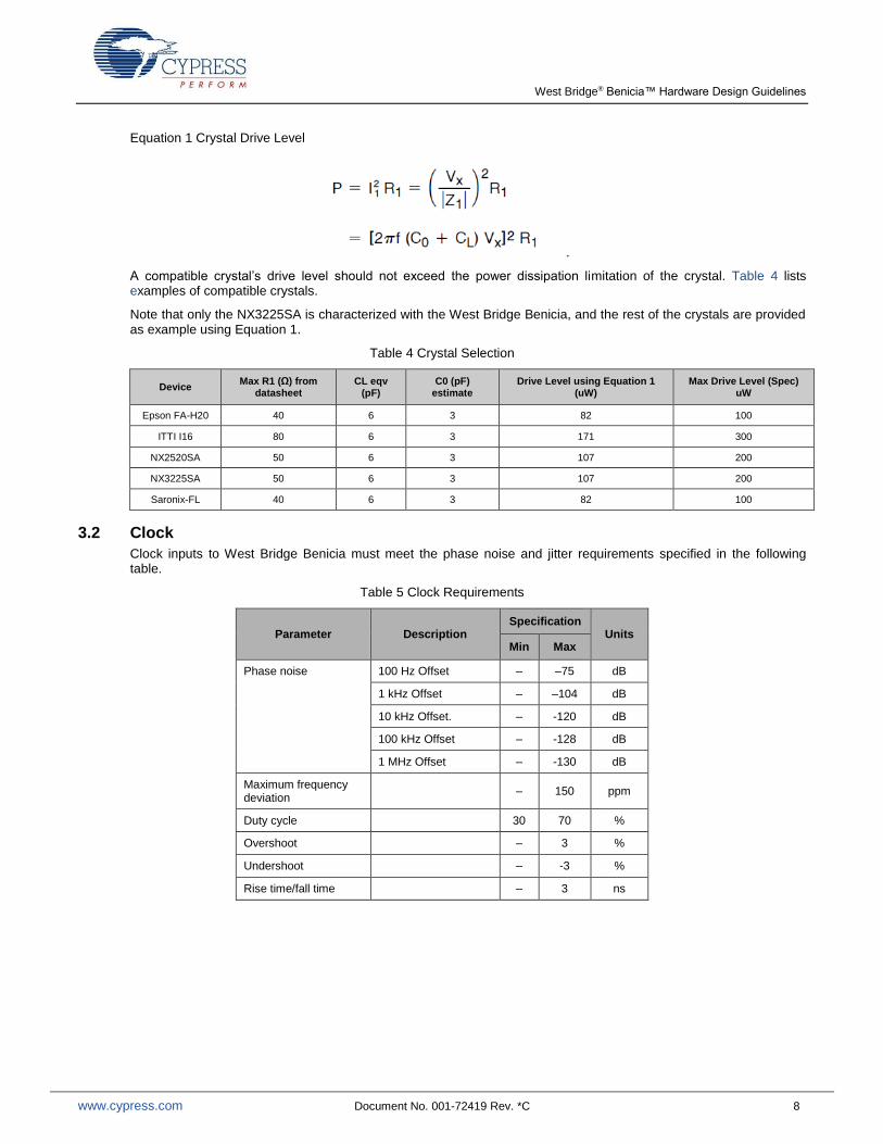
A compatible crystal’s drive level should not exceed the power dissipation limitation of the crystal. Table 4 lists examples of compatible crystals.
Note that only the NX3225SA is characterized with the West Bridge Benicia, and the rest of the crystals are provided as example using Equation 1.
Table 4 Crystal Selection
Device Max R1 (Ω) from
datasheet CL eqv
(pF) C0 (pF)
estimate Drive Level using Equation 1
(uW) Max Drive Level (Spec)
uW
Epson FA-H20 40 6 3 82 100
ITTI I16 80 6 3 171 300
NX2520SA 50 6 3 107 200
NX3225SA 50 6 3 107 200
Saronix-FL 40 6 3 82 100
3.2 Clock
Clock inputs to West Bridge Benicia must meet the phase noise and jitter requirements specified in the following table.
Table 5 Clock Requirements
Parameter Description Specification
Units Min Max
Phase noise 100 Hz Offset – –75 dB
1 kHz Offset – –104 dB
10 kHz Offset. – -120 dB
100 kHz Offset – -128 dB
1 MHz Offset – -130 dB
Maximum frequency deviation
– 150 ppm
Duty cycle 30 70 %
Overshoot – 3 %
Undershoot – -3 %
Rise time/fall time – 3 ns
West Bridge® Benicia™ Hardware Design Guidelines
www.cypress.com Document No. 001-72419 Rev. *C 9
3.3 Frequency Select
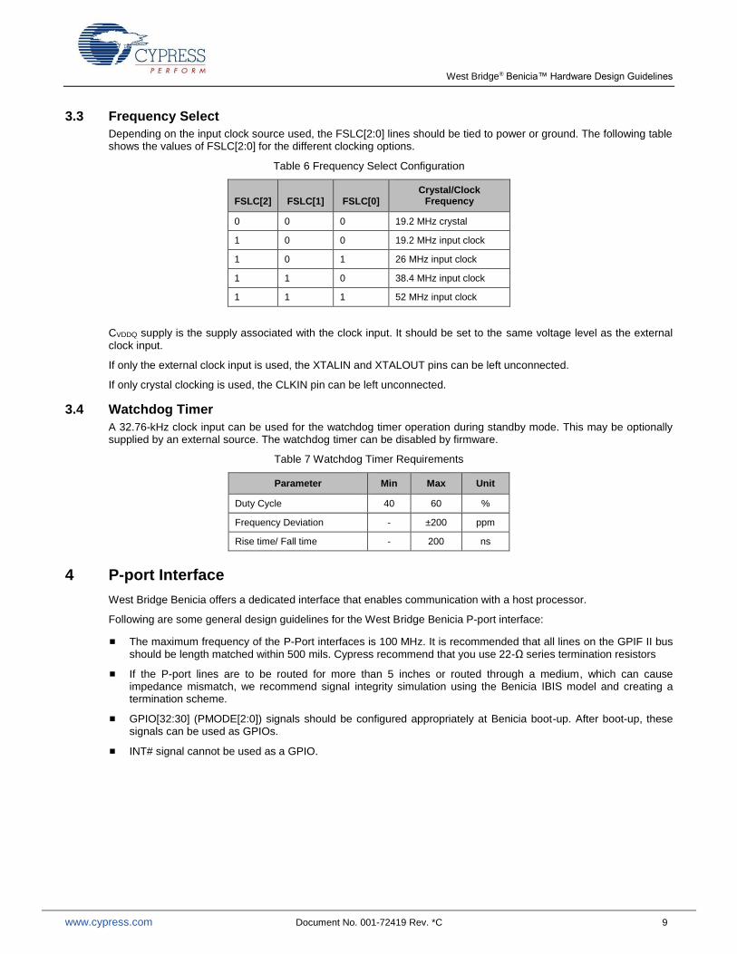
Depending on the input clock source used, the FSLC[2:0] lines should be tied to power or ground. The following table shows the values of FSLC[2:0] for the different clocking options.
Table 6 Frequency Select Configuration
FSLC[2] FSLC[1] FSLC[0] Crystal/Clock
Frequency
0 0 0 19.2 MHz crystal
1 0 0 19.2 MHz input clock
1 0 1 26 MHz input clock
1 1 0 38.4 MHz input clock
1 1 1 52 MHz input clock
CVDDQ supply is the supply associated with the clock input. It should be set to the same voltage level as the external clock input.
If only the external clock input is used, the XTALIN and XTALOUT pins can be left unconnected.
If only crystal clocking is used, the CLKIN pin can be left unconnected.
3.4 Watchdog Timer
A 32.76-kHz clock input can be used for the watchdog timer operation during standby mode. This may be optionally supplied by an external source. The watchdog timer can be disabled by firmware.
Table 7 Watchdog Timer Requirements
Parameter Min Max Unit
Duty Cycle 40 60 %
Frequency Deviation - ±200 ppm
Rise time/ Fall time - 200 ns
4 P-port Interface
West Bridge Benicia offers a dedicated interface that enables communication with a host processor.
Following are some general design guidelines for the West Bridge Benicia P-port interface:
The maximum frequency of the P-Port interfaces is 100 MHz. It is recommended that all lines on the GPIF II bus should be length matched within 500 mils. Cypress recommend that you use 22-Ω series termination resistors
If the P-port lines are to be routed for more than 5 inches or routed through a medium, which can cause impedance mismatch, we recommend signal integrity simulation using the Benicia IBIS model and creating a termination scheme.
GPIO[32:30] (PMODE[2:0]) signals should be configured appropriately at Benicia boot-up. After boot-up, these signals can be used as GPIOs.
INT# signal cannot be used as a GPIO.

West Bridge® Benicia™ Hardware Design Guidelines
www.cypress.com Document No. 001-72419 Rev. *C 10
5 S-port Interface
West Bridge Benicia has two independent storage ports (S0-port and S1-port). Both storage ports support the following:
MMC-system specification, MMCA Technical Committee, Version 4.4
SD specification Version, 3.0
SDIO host controller compliant with SDIO specification Version 2.00 (Jan 30, 2007)
To satisfy the tight requirements of these specifications, the following guidelines should be followed while designing the storage port circuitry on a West Bridge Benicia system PCB.
All data lines, and command and clock lines should be length matched.
The trace lengths should be at least 3.2 inches and not more than 5 inches. These numbers are calculated based on the worst-case timing parameters for SD cards, eMMC devices, and the West Bridge Benicia device and should be taken only as a recommendation.
In the case of SD card, the VDD (pin 9 of SD socket) should be tied to 3.3 V regardless of the I/O voltage used on the other SD lines, as illustrated in Figure 11.
In case of an eMMC device, VCC should be tied to 3.3 V and VCC should be tied to the port I/O voltage supply (S0VDDQ or S1VDDQ). Figure 12 shows an eMMC device circuit.
Add a 10 KΩ pull-up resistor to the SD data signals, except for SD_D3, which is used as one of the card insertion’s detect mechanism. A 470 K is used to pull down SD_DQ3. SD_CLK is pulled up using only a 1 KΩ resistor.
Card insertion and removal detection is provided using the following mechanisms:
SD-D3 data line: SD cards have an internal 10-kΩ pull-up resistor. When you insert or remove the card from the SD/MMC connector, the voltage level at the SD_D3 pin changes and triggers an interrupt to the CPU. Note that older generations of MMC cards do not support this card detection mechanism.
S0/S1_INS pin: Some SD/MMC connectors facilitate a micro switch for card insertion and removal detection. This micro switch can be connected to S0/S1_INS. When you insert or remove the card from the SD/MMC connector, it turns the micro switch on and off. This changes the voltage level at the pin that triggers the interrupt to the CPU. Note that this S0/S1_INS pin is shared between the two S-Ports. Register configuration determines which port gets to use this pin. This pin is mapped to the S1VDDQ power domain; if S0VDDQ and S1VDDQ are at different voltage levels, this pin cannot be used as S1_INS. The insertion/removal detection mechanism is not used for eMMC devices because the devices are usually soldered on the board and do not involve insertion/removal detection.
The following figures show different implementation of the SD cards and eMMC devices.
Figure 11. SD Card Circuit

West Bridge® Benicia™ Hardware Design Guidelines
www.cypress.com Document No. 001-72419 Rev. *C 11
Figure 12. eMMC Device Circuit
6 Low Performance Peripherals (LPP)
6.1 I2C Interface
West Bridge Benicia’s I2C interface is compatible with the I2C Bus Specification Revision 3. The interface is capable of operating as I2C Master only. For example, West Bridge Benicia may boot from an EEPROM connected to the I2C interface, as a selectable boot option. West Bridge Benicia’s I2C Master Controller also supports multi-master mode functionality.
The power supply for the I2C interface is I2CVDDQ, which is a separate power domain from the other serial peripherals. This is to allow the I2C interface the flexibility to operate at a different voltage than the other serial interfaces.
The bus frequencies supported by the I2C controller are 100 kHz, 400 kHz, and 1 MHz. When I2CVDDQ is 1.2 V, the maximum operating frequency supported is 100 kHz. When I2CVDDQ is 1.8 V, 2.5 V, or 3.3 V, the operating frequencies supported are 400 kHz and 1 MHz.
Both SCL and SDA signals of the I2C interface require external pull-up resistors. The pull-up resistors must be connected to I2CVDDQ as shown in Figure 13.
Figure 13. I2C Configuration

West Bridge® Benicia™ Hardware Design Guidelines
www.cypress.com Document No. 001-72419 Rev. *C 12
6.2 JTAG
West Bridge Benicia has a JTAG interface to provide a standard five-pin interface for connecting to a JTAG debugger. This feature enables debugging of the firmware through the CPU core's on-chip debug circuitry. There is no need for external pull up or pull-down on the JTAG signals as the JTAG signals (TDI, TMC, TRST# signals) have fixed 50-kΩ internal pull-ups and the TCK signal has a fixed 10-kΩ pull-down resistor.
6.3 I2S
West Bridge Benicia has an I2S port to support external audio codec devices. It functions as an I2S master (transmitter only). The I2S interface consists of four signals: clock line (I2S_CLK), serial data line (I2S_SD), word select line (I2S_WS), and master system clock (I2S_MCLK). Benicia can generate the system clock as an output on I2S_MCLK or accept an external-system clock input on I2S_MCLK. The I2S interface supports sampling frequencies of 32 kHz, 44.1 kHz, and 48 kHz.
6.4 SPI and UART
West Bridge Benicia supports an SPI master interface on the serial peripherals port. The SPI GPIOs are shared with the UART GPIOs. There should be no pull up or pull-down on MOSI and MISO signals. Figure 14 shows the correct SPI signal connection using the M25P40-VMN6TPB SPI device.
Figure 14. SPI Configuration
7 Booting
West Bridge Benicia can load boot images from various sources. It can be the main processor in a system or a co-processor. The booting option depends on the specific system implementation. PMODE[2:0] configures the boot option and can be connected directly to the external processor on the p-port or hardwired on the board depending on the booting option that is used. The following table shows the levels of the PMODE[2:0] signals required for the different booting options.
Table 8. PMODE Signal Setting
PMODE[2:0] Boot From
000 S0-port (eMMC) On failure, USB boot is enabled
001 PMMC pass through On failure, USB boot is enabled
010 PMMC pass through
011 PMMC relay (enables secure boot)
100 S0-port (eMMC)
101 Sync ADMUX (16 bit data bus)
110 PMMC legacy
111 USB boot
00Z Async SRAM (16 bit data bus)
01Z Async ADMUX (16 bit data bus)
West Bridge® Benicia™ Hardware Design Guidelines
www.cypress.com Document No. 001-72419 Rev. *C 13
PMODE[2:0] Boot From
10Z I2C On failure, USB boot is enabled
11Z I2C only
1Z1 PMMC relay (enables secure boot) On failure, USB boot is enabled
Note Z = High-Z, Open drain, No connect
Cypress recommends that you add pull-up and pull-down options on the PMODE[2:0] signals and load the combination needed for the preferred booting option. This gives the flexibility to debug the system during early development.
Contact Cypress technical support (www.cypress.com > Design Support > Create a Customer Case) for more information on boot options, EEPROM size required etc.
8 EMI and ESD Considerations
EMI and ESD should be considered on a case-by-case basis, relative to the product enclosure, deployment environment, and regulatory statutes. Though this application note does not give specific recommendations regarding EMI, West Bridge Benicia meets EMI requirements outlined by FCC 15B (USA) and EN55022 (Europe) for consumer electronics. West Bridge Benicia can tolerate reasonable EMI, which is conducted by the aggressor, outlined in the above specifications and continue to function as expected. However this application note gives general EMI and ESD considerations. Refer to Appendix A – PCB Layout Tips for general information on PCB layout techniques. Refer to ‘AN61290 – PSoC® 3 and PSoC 5 Hardware Design Considerations’, which has a list of layout tips to improve EMI/EMC and suggests reference books on this topic.
West Bridge Benicia has built-in ESD protection on the D+, D–, and GND pins on the USB interface. The ESD protection levels given on these ports are:
±2.2 kV Human Body Model (HBM) based on the JESD22-A114 Specification.
±6 kV Contact Discharge and ±8 kV Air Gap Discharge based on IEC61000-4-2 level 3A.
±8 kV Contact Discharge and ±15 kV Air Gap Discharge based on IEC61000-4-2 level 4C.
This protection ensures that the device continues to function after ESD events up to the levels stated.
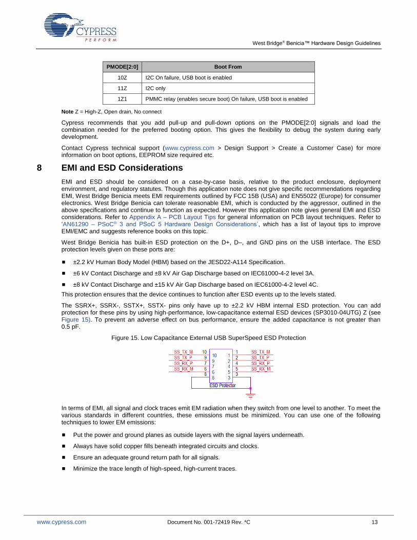
The SSRX+, SSRX-, SSTX+, SSTX- pins only have up to ±2.2 kV HBM internal ESD protection. You can add protection for these pins by using high-performance, low-capacitance external ESD devices (SP3010-04UTG) Z (see Figure 15). To prevent an adverse effect on bus performance, ensure the added capacitance is not greater than 0.5 pF.
Figure 15. Low Capacitance External USB SuperSpeed ESD Protection
In terms of EMI, all signal and clock traces emit EM radiation when they switch from one level to another. To meet the various standards in different countries, these emissions must be minimized. You can use one of the following techniques to lower EM emissions:
Put the power and ground planes as outside layers with the signal layers underneath.
Always have solid copper fills beneath integrated circuits and clocks.
Ensure an adequate ground return path for all signals.
Minimize the trace length of high-speed, high-current traces.

West Bridge® Benicia™ Hardware Design Guidelines
www.cypress.com Document No. 001-72419 Rev. *C 14
9 Benicia Device Package Dimensions
West Bridge Benicia is packaged on a 4.659 × 5.099 mm, 0.4-mm pitch chip scale package (CSP). The recommended pad size is 0.2077 mm (8.18 mils).
Figure 16. West Bridge Benicia Package Dimension
10 Electrical Design Consideration
USB 3.0 protocol enhances USB speed up to 5 Gbps. By including SuperSpeed lines along with High Speed lines, it is backward compatible with the USB 2.0 specification. Both buses require a greater level of attention to electrical design. Careful attention to component selection, supply decoupling, signal line impedance, and noise are required when designing for SuperSpeed USB. These physical issues are mostly affected by the PCB design. Refer to Appendix A – PCB Layout Tips for general information on PCB layout techniques.
10.1 USB 3.0 SuperSpeed Design Guidelines
West Bridge Benicia has SuperSpeed USB lines and High Speed USB lines. Use the following best practices when designing with these busses (for detailed high speed routing guidelines, see AN1168 - High-Speed USB PCB Layout Recommendations):
Minimize USB lines. These should be routed first to make sure certain recommendations on this list are achievable. Long traces affect the transmitter quality and introduce inter-symbol interference (ISI) on the receive side.
The polarity can be swapped on the USB 3.0 differential pairs. Polarity detection is done automatically by the USB 3.0 PHY during link training, as defined in the USB 3.0 specification section 6.4.2, and does not require any additional changes to device firmware. Because the USB connector pinout is defined, this is a mechanism to ensure that these traces do not cross each other.
Tie the R_USB2 pin to ground through a 1% 6.04-kΩ precision resistor. R_USB3 pin should be tied to ground through a 1% 200-Ω precision resistor.
Figure 17. USB2 and USB3 Reference Resistors
USB 3.0 traces require additional AC coupling capacitors (0.1 µF) placed on the SS_TX lines. Place these capacitors symmetrically and close to the Benicia device as shown in the following figure.

West Bridge® Benicia™ Hardware Design Guidelines
www.cypress.com Document No. 001-72419 Rev. *C 15
Figure 18. SuperSpeed TX Line Decoupling Caps
Two immediate planes under these AC coupling capacitors should have a cutout in the shape of these capacitors to avoid extra capacitance on the lines because of the capacitor pads. The following figure shows the proper layout of the decoupling caps.
Figure 19. SuperSpeed TX decoupling Caps Layout
Recommended
Plane cut out under caps
Not recommended
USB signal line impedance should be 90 Ω differential (±7%).
Keep trace spacing between differential pairs constant to avoid impedance mismatches.
Figure 20. Differential Pairs Impedance Matching Techniques
Not recommended
Not recommended
Recommended
All SS signal lines should be routed entirely over a solid ground plane on an adjacent layer. Splitting the ground plane under the SS signals introduces impedance mismatches and increases electrical emissions. The following figure shows a solid ground plain under the SuperSpeed signal.

West Bridge® Benicia™ Hardware Design Guidelines
www.cypress.com Document No. 001-72419 Rev. *C 16
Figure 21. Solid Ground Plain under the SuperSpeed Signal
SS trace
Signal layer
Ground layer
Differential SS pair trace lengths should be matched within 0.12 mm (5 mils). The HS D+ and D– signal trace lengths should be matched within 1.25 mm (50 mils). Adjustment for HS signals should be made near the receptacle, if necessary. Adjustments for SS Rx signals should be made near the USB 3.0 receptacle, while adjustments for SS Tx signals should be made near the device, if necessary. An example for length matching for the SuperSpeed signal is shown in the following figure.
Figure 22. SuperSpeed Signal Length Matching
The number of layers on the PCB should be at least four. Use a solid reference power plane to maintain 90 Ω differential impedance.
When two pairs of USB traces cross each other in different layers, a ground layer should run all the way between the two USB signal layers as illustrated in the following figure.
Figure 23. Ground Insertion
SS traces on top layer
Top signal layer
Ground layer b/w signal
layers
Inner signal layer
Crossing SS traces on inner
layer
USB 3.0
Receptacle Rx lines
USB 3.0 device
Tx lines
West Bridge® Benicia™ Hardware Design Guidelines
www.cypress.com Document No. 001-72419 Rev. *C 17
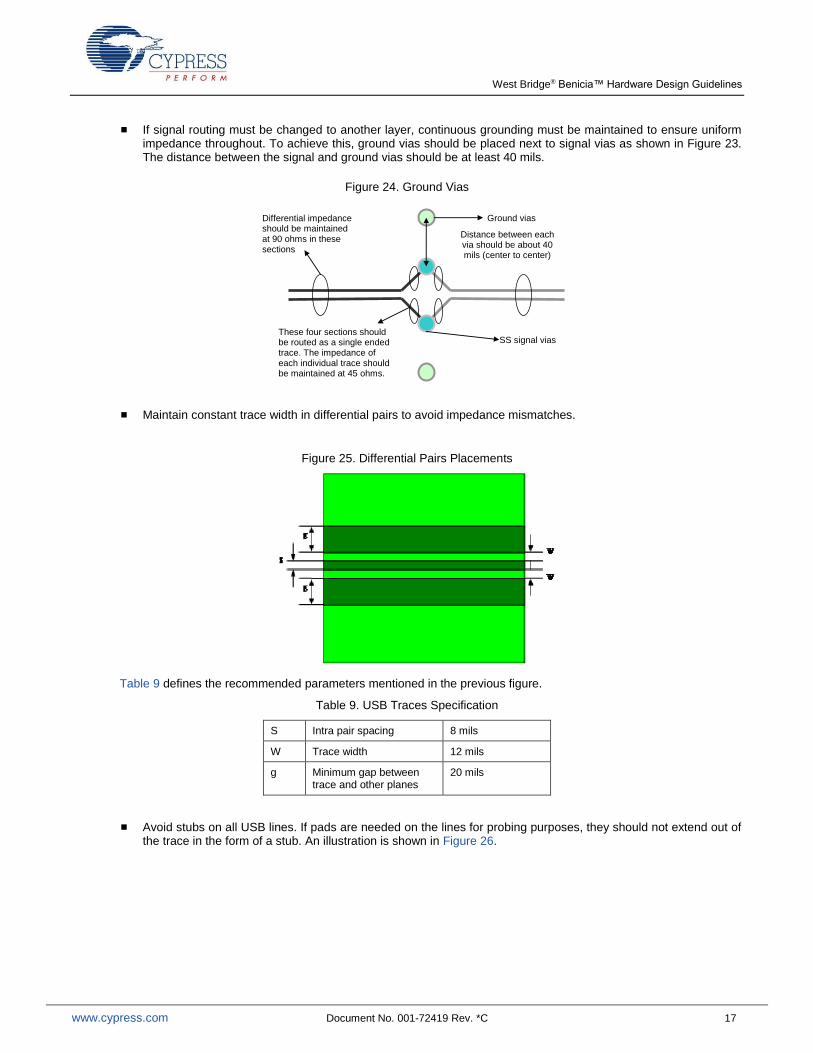
If signal routing must be changed to another layer, continuous grounding must be maintained to ensure uniform impedance throughout. To achieve this, ground vias should be placed next to signal vias as shown in Figure 23. The distance between the signal and ground vias should be at least 40 mils.
Figure 24. Ground Vias
Ground vias
SS signal vias
Distance between each via should be about 40 mils (center to center)
These four sections should be routed as a single ended trace. The impedance of each individual trace should be maintained at 45 ohms.
Differential impedance should be maintained at 90 ohms in these sections
Maintain constant trace width in differential pairs to avoid impedance mismatches.
Figure 25. Differential Pairs Placements
Table 9 defines the recommended parameters mentioned in the previous figure.
Table 9. USB Traces Specification
S Intra pair spacing 8 mils
W Trace width 12 mils
g Minimum gap between trace and other planes
20 mils
Avoid stubs on all USB lines. If pads are needed on the lines for probing purposes, they should not extend out of the trace in the form of a stub. An illustration is shown in Figure 26.

West Bridge® Benicia™ Hardware Design Guidelines
www.cypress.com Document No. 001-72419 Rev. *C 18
Figure 26. Probing Pads Placement
Recommended
Not recommended
Probe pads
Stubs
Void for vias on the SS signal lines should be common for the differential pair. Having a common void, as shown in the following figure, maintains better impedance matching in comparison to separate vias.
Figure 27. Void VIAS Placement For SS Traces
Distance between each via pair should be about 40 mils.
Void in plane for vias
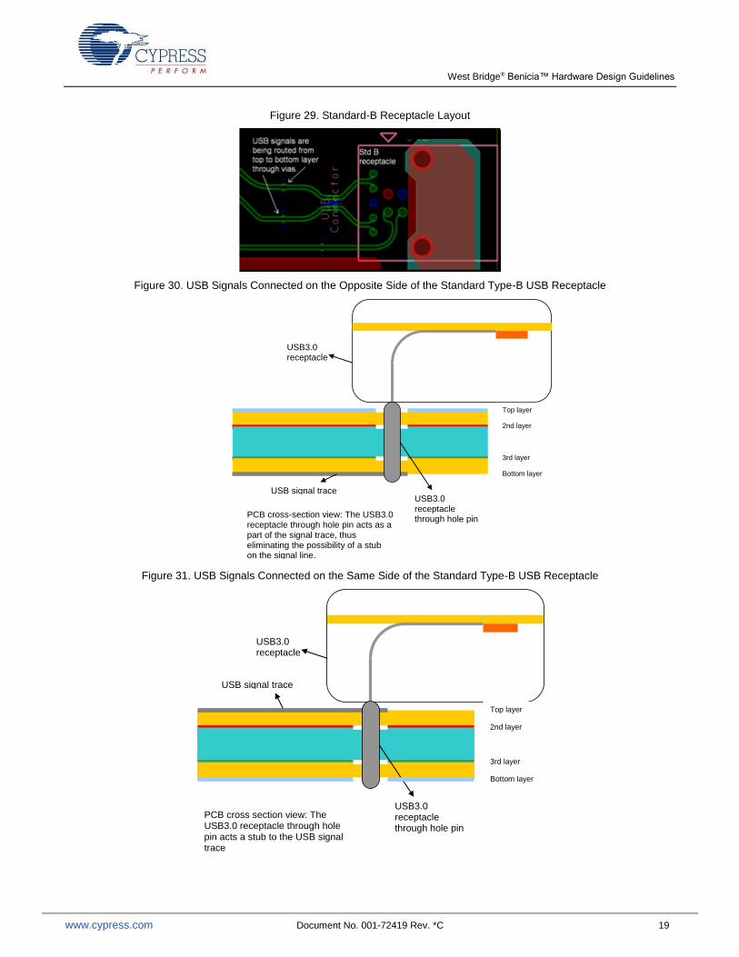
Cypress recommends that, when using a Type B receptacle (through a hole receptacle), you must connect the USB signal lines to the receptacle pins on the opposite layer of where the receptacle is placed (see Figure 28 and Figure 29). For example, if the Type B receptacle is placed on the top layer, the signal lines should connect to the receptacle pins on the bottom layer. This prevents the unnecessary stubs due to the USB receptacle pins. A diagram of the recommended layout versus the stub producing layout is illustrated in Figure 30 and Figure 31 respectively.
Figure 28. Standard-B Receptacle Placement
West Bridge® Benicia™ Hardware Design Guidelines
www.cypress.com Document No. 001-72419 Rev. *C 19
Figure 29. Standard-B Receptacle Layout
Figure 30. USB Signals Connected on the Opposite Side of the Standard Type-B USB Receptacle
Top layer
2nd layer
3rd layer
Bottom layer
USB3.0 receptacle
USB signal trace USB3.0 receptacle through hole pin
PCB cross-section view: The USB3.0 receptacle through hole pin acts as a part of the signal trace, thus eliminating the possibility of a stub on the signal line.
Figure 31. USB Signals Connected on the Same Side of the Standard Type-B USB Receptacle
Top layer
2nd layer
3rd layer
Bottom layer
USB3.0 receptacle
USB signal trace
USB3.0 receptacle through hole pin
PCB cross section view: The USB3.0 receptacle through hole pin acts a stub to the USB signal trace

West Bridge® Benicia™ Hardware Design Guidelines
www.cypress.com Document No. 001-72419 Rev. *C 20
Connect the “shield” pins on the USB 3.0 receptacle to ground through an inductor for AC isolation.
On the USB signal lines, use as few bends as possible. Avoid 90-degree bends. If bends are necessary, use 45 degrees or rounded (curved) bends as illustrated in the following figure.
Figure 32. USB Signal Bends
Not recommended
Recommended
Recommended
To avoid crosstalk, do not place the differential pairs close to other differential pairs, clock signals, or any other high-speed signals.
The following four images (Figure 33 through Figure 36) show an example of routing the USB signals from the device to the receptacle.
The SS_Rx signals are routed on the top layer while the SS_Tx signals are routed on the bottom layer. The SS_Rx signals come out of the device in 2.5 mils width because of the small pitch of the Benicia device. After the device area is cleared, the trace width increases to 11 mils. The SS_Tx signal traces come out of the device on the bottom layer in 2.5 mils width. After the device area is cleared, the width increases to 11 mils. The SS_Tx signals finally route back to the top layer (same layer as the USB 3.0 receptacle) through vias. The D+ and D- signals are shown in Figure 35.

West Bridge® Benicia™ Hardware Design Guidelines
www.cypress.com Document No. 001-72419 Rev. *C 21
The following table shows the trace width recommendations for optimal signal routing.
Table 10. USB Traces Specification
Trace Width Air Gap
Inside package area 2.5 mils 2.5 mils
Outside package area 11 mils on top, 4.25 mils in inner layers
9 mils on top, 10.75 mils in inner layers
Figure 33. USB Signals Layout Example
Figure 34. USB Signals Layout Example

West Bridge® Benicia™ Hardware Design Guidelines
www.cypress.com Document No. 001-72419 Rev. *C 22
Figure 35. USB Signals Layout Example
Figure 36. USB Signals Layout Example

West Bridge® Benicia™ Hardware Design Guidelines
www.cypress.com Document No. 001-72419 Rev. *C 23
A Appendix A – PCB Layout Tips There are many classic techniques for designing PCBs for low noise and EMC. Some of the techniques are as follows:
Multiple layers: Although they are more expensive, it is best to use a multi-layer PCB with separate layers
dedicated to the VSS and VDD supplies. This gives good decoupling and shielding effects. Separate fills on these layers should be provided for VSSA, VSSD, VDDA, and VDDD.
To reduce cost, a 2-layer or even a single-layer PCB can be used. In that case, you must have a good layout for all VSS and VDD.
Component Position: You should separate the different circuits on the PCB according to their electromagnetic
interference (EMI) contribution. This helps to reduce cross-coupling on the PCB. For example, you should separate noisy high current circuits, low voltage circuits, and digital components.
Ground and Power Supply: There should be a single point for gathering all ground returns. Avoid ground loops
or minimize their surface area. All component-free surfaces of the PCB should be filled with additional grounding to create a shield, especially when using 2-layer or single-layer PCBs.
The power supply should be close to the ground line to minimize the area of the supply loop. The supply loop can act as an antenna and can be a major emitter or receiver of EMI.
Decoupling: The standard decoupler for external power is a 100-μF capacitor. Supplementary 0.1-μF capacitors
should be placed as close as possible to the VSS and VDD pins of the device, to reduce high frequency power supply ripple.
Generally, you should decouple all sensitive or noisy signals to improve electromagnetic compatibility (EMC) performance. Decoupling can be both capacitive and inductive.
Signal Routing: When designing an application, study the following areas closely to improve EMC performance:
Noisy signals (for example, signals with fast edge times)
Sensitive and high-impedance signals
Signals that capture events, such as interrupts and strobe signals
To increase EMC performance, keep the trace lengths as short as possible and isolate the traces with VSS
traces. To avoid crosstalk, do not route them near to or parallel to other noisy and sensitive traces. For more information, several references are available:
The Circuit Designer's Companion, Second Edition, (EDN Series for Design Engineers) by Tim Williams
PCB Design for Real-World EMI Control (The Springer International Series in Engineering and Computer Science), by Bruce R. Archambeault and James Drewniak
Printed Circuits Handbook (McGraw Hill Handbooks), by Clyde Coombs
EMC and the Printed Circuit Board: Design, Theory, and Layout Made Simple, by Mark I. Montrose
Signal Integrity Issues and Printed Circuit Board Design, by Douglas Brooks

West Bridge® Benicia™ Hardware Design Guidelines
www.cypress.com Document No. 001-72419 Rev. *C 24
Document History
Document Title: AN72419 - West Bridge® Benicia™ Hardware Design Guidelines and Schematic Checklist
Document Number: 001-72419
Revision ECN Orig. of Change
Submission Date
Description of Change
** 3407282 MRKA 10/18/2011 New application note.
*A 3537155 MRKA 02/28/2012 1. Added schematic design checklist section; also added ‘Schematic Checklist’ to the title.
2. Changed U3TXVDDQ and U3RXVDDQ decoupling cap values to 22 µF.
3. Added P-port interface guidelines.
4. Changed heading of Benicia package section to ‘Benicia Device Package Dimensions.’
*B 3794475 ROSM 11/26/2012 Added Power block diagram
Changed the VBUS min to 4.0 V
Replaced the “F” symbol in the Booting section with High-Z
Added Crystal and Clock specification and added a list of compatible crystals
Added Inrush Consideration and Power Supply Design section
Added decoupling cap placement sample
Added values for termination resistors
Changed the 32.768 kHz clock input to standby mode support
Added ESD part number and placement example
Updated the loading capacitance requirements for the external USB 3.0 ESD
Added the location of USB3.0 Polarity Inversion section in the USB 3.0 Spec
Added LLP interface I2C, SPI/UART, I2S Consideration
Added Appendix A.
*C 4874828 RAGO 08/06/2015 Updated template
West Bridge® Benicia™ Hardware Design Guidelines
www.cypress.com Document No. 001-72419 Rev. *C 25
Worldwide Sales and Design Support
Cypress maintains a worldwide network of offices, solution centers, manufacturer’s representatives, and distributors. To find the office closest to you, visit us at Cypress Locations.
Products
Automotive cypress.com/go/automotive
Clocks & Buffers cypress.com/go/clocks
Interface cypress.com/go/interface
Lighting & Power Control cypress.com/go/powerpsoc
Memory cypress.com/go/memory
PSoC cypress.com/go/psoc
Touch Sensing cypress.com/go/touch
USB Controllers cypress.com/go/usb
Wireless/RF cypress.com/go/wireless
PSoC® Solutions
psoc.cypress.com/solutions
PSoC 1 | PSoC 3 | PSoC 4 | PSoC 5LP
Cypress Developer Community
Community | Forums | Blogs | Video | Training
Technical Support
cypress.com/go/support
PSoC is a registered trademark and PSoC Creator is a trademark of Cypress Semiconductor Corp. All other trademarks or registered trademarks referenced herein are the property of their respective owners.
Cypress Semiconductor 198 Champion Court San Jose, CA 95134-1709
Phone : 408-943-2600 Fax : 408-943-4730 Website : www.cypress.com
© Cypress Semiconductor Corporation, 2011-2015. The information contained herein is subject to change without notice. Cypress Semiconductor Corporation assumes no responsibility for the use of any circuitry other than circuitry embodied in a Cypress product. Nor does it convey or imply any license under patent or other rights. Cypress products are not warranted nor intended to be used for medical, life support, life saving, critical control or safety applications, unless pursuant to an express written agreement with Cypress. Furthermore, Cypress does not authorize its products for use as critical components in life-support systems where a malfunction or failure may reasonably be expected to result in significant injury to the user. The inclusion of Cypress products in life-support systems application implies that the manufacturer assumes all risk of such use and in doing so indemnifies Cypress against all charges. This Source Code (software and/or firmware) is owned by Cypress Semiconductor Corporation (Cypress) and is protected by and subject to worldwide patent protection (United States and foreign), United States copyright laws and international treaty provisions. Cypress hereby grants to licensee a personal, non-exclusive, non-transferable license to copy, use, modify, create derivative works of, and compile the Cypress Source Code and derivative works for the sole purpose of creating custom software and or firmware in support of licensee product to be used only in conjunction with a Cypress integrated circuit as specified in the applicable agreement. Any reproduction, modification, translation, compilation, or representation of this Source Code except as specified above is prohibited without the express written permission of Cypress. Disclaimer: CYPRESS MAKES NO WARRANTY OF ANY KIND, EXPRESS OR IMPLIED, WITH REGARD TO THIS MATERIAL, INCLUDING, BUT NOT LIMITED TO, THE IMPLIED WARRANTIES OF MERCHANTABILITY AND FITNESS FOR A PARTICULAR PURPOSE. Cypress reserves the right to make changes without further notice to the materials described herein. Cypress does not assume any liability arising out of the application or use of any product or circuit described herein. Cypress does not authorize its products for use as critical components in life-support systems where a malfunction or failure may reasonably be expected to result in significant injury to the user. The inclusion of Cypress’ product in a life-support systems application implies that the manufacturer assumes all risk of such use and in doing so indemnifies Cypress against all charges. Use may be limited by and subject to the applicable Cypress software license agreement.
Related Documents