ECE280: Nano-Plasmonics and Its Applications Week1 Week1 Basics for Plasmonics Basics for Plasmonics

Welcome message from author
This document is posted to help you gain knowledge. Please leave a comment to let me know what you think about it! Share it to your friends and learn new things together.
Transcript
ECE280: Nano-Plasmonics and Its Applications
Week1Week1
Basics for PlasmonicsBasics for Plasmonics

Light Matter InteractionsLight Matter Interactions
Incident light
reflected light
transmitted lightpropagation through the medium
General Phenomena
refraction absorption and luminescence
scattering
Phenomena that can occur as a light beam propagates through an optical medium

• Crystalline insulators and semiconductors
• Glasses
• Metals
• Molecular Materials
• Doped glasses and insulators
Optical Materials Optical Materials

SilverSilver
Electron shell diagram
Among metals, pure silver has the highest thermal conductivity, the whitest color,and the highest optical reflectivity.
Major Applications
Photography
Jewelry
Industrial
Coins & medals
24%
33%
40%
3%
Based on data in 2001

Dielectric Constant for MetalsDielectric Constant for Metals
tieeEteEdtdxm
dtxdm ωγ −−=−=+ 002
2
0 )(
)()()( 2
0 γωω imteEtx+
=
Drude-Lorentz model:
tiexx ω−= 0
)( 20
2
000 γωωεεεε
imENeEPEED r +
−=+==
NexP −=
)(11)( 2
00
2
γωωεωε
imNe
r +−=
"i' , ,)(
1)( r00
2
p2
2
εεεε
ωγωω
ωωε +==
+−=
mNe
ip
r

ExamplesExamples
0.2 0.4 0.6 0.8 1-50
-40
-30
-20
-10
0
Wavelength (um)
Per
mit
tivi
tyAg
Real part
Imaginary part

EE--M wave at the interface (1)M wave at the interface (1)
Consider a p-polarized wave propagates in z-x plane:
Z>0 H2 = (0,Hy2,0)exp(ikx2x+ikz2z-iωt)E2 = (Ex2,0,Ez2)exp(ikx2x+ikz2z-iωt)
Z<0 H1 = (0,Hy1,0)exp(ikx1x+ikz1z-iωt)E1 = (Ex1,0,Ez1)exp(ikx1x+ikz1z-iωt)
1i i iH E
c tε ∂
∇× =∂
v v v
1i iE H
c t∂
∇× = −∂
v v v
0i iEε ∇ ⋅ =v v
0iH∇⋅ =v v
Maxwell’s equations: (μ=1)
Media 1
k2
k1
z
x
Media 2

ˆ ˆ ˆ1
ˆˆexp( ) exp( ) ( ,0, )exp( )
( ,0, )exp( ) ( ,0, )exp( )
x y z
x y x z z y x z x z x z
z y x y x z x z x z
x y z
Ex y z c t
H H H
ik H ik x ik z i t z ik H ik x ik z i t x i E E ik x ik z i tc
k H k H ik x ik z i t E E ik x ik z i tc
H ε
ωω ω ε ω
ωω ε ω
∂ ∂ ∂ ∂= =∂ ∂ ∂ ∂
⋅ + − − ⋅ + − = − + −
− + − = − + −
∇×v vuv
Boundary condition:Ex1=Ex2, Hy1=Hy2, ε1Ez1= ε2Ez2
2 22 2 2
2 2y x z
z x
H E Ek c k cε ω ε ω
= = −1 11 1 1
1 1y x z
z x
H E Ek c k cε ω ε ω
= = −
kx1=kx2=kx kz1/ ε1= kz2/ ε2
EE--M wave at the interface (2)M wave at the interface (2)

also, 2 2 2( )xi zi ik kcωε+ =
EE--M wave at the interface (3)M wave at the interface (3)
2 22 211 1
2 22 22 2
2
( )
( )
xz
zx
kk ck k
c
ωε εω εε
−= =
−
We have:
22
1 2 1 2 1 2 1 22( )( ) ( )xkcωε ε ε ε ε ε ε ε+ − = −

EE--M wave at the interface (4)M wave at the interface (4)
Case 1:
1 2k k=v v
1 2ε ε=
Media 1
k2
k1
z
x
Media 2
Means homogeneous media
kx= any allowed value
1 2( ) 0ε ε− =

EE--M wave at the interface (5)M wave at the interface (5)
12
1 2
1 2xk real number
cω ε ε
ε ε⎛ ⎞
= =⎜ ⎟+⎝ ⎠
1 2( ) 0ε ε− ≠ 1 2, 0ε ε >Case 2: and
1 2ε ε=
Media 1
k2
k1
z
x
Media 212 2
11
1 2zk
cω ε
ε ε⎛ ⎞
= ⎜ ⎟+⎝ ⎠
12 2
22
1 2zk
cω ε
ε ε⎛ ⎞
= ⎜ ⎟+⎝ ⎠
We have:
θ
21 2
1 11
tan( ) x
z
k nk n
εθ
ε= = =
The Brewster angle !

EE--M wave at the interface (6)M wave at the interface (6)
1 2 0ε ε <Case 3: and 1 2 0ε ε+ >
1122
1 21 2
1 2 1 2xk i imaginary number
c cε εω ε ε ω
ε ε ε ε⎛ ⎞⎛ ⎞
= = =⎜ ⎟⎜ ⎟+ +⎝ ⎠ ⎝ ⎠
We have:
Exponentially increase in -X direction !
Since the media in -x direction is infinite, the EM field will diverge, which means the solution is non-physical.

EE--M wave at the interface (7)M wave at the interface (7)
12
1 2
1 2xk real number
cω ε ε
ε ε⎛ ⎞
= =⎜ ⎟+⎝ ⎠
1 20, 0ε ε> <Case 4: and 1 2 0ε ε+ <
We have:
122
11
1 2zk i imaginary number
cω ε
ε ε⎛ ⎞
= − =⎜ ⎟+⎝ ⎠
122
22
1 2zk i imaginary number
cω ε
ε ε⎛ ⎞
= =⎜ ⎟+⎝ ⎠
EM wave propagates in x direction, but exponentially decays awayfrom the interface ! This is called the surface plasma.
Media 1
kx2
kx1
z
x
Media 2ε2<0
ε1>0
kz2
kz1

Surface Surface PlasmonsPlasmons
2/1
21
21⎟⎟⎠
⎞⎜⎜⎝
⎛+
=εε
εεωc
k x
21
21
'''εεεεω+
=c
k x 21
1
2/3
21
21
)'(2"
''
"εε
εεεεω
⎟⎟⎠
⎞⎜⎜⎝
⎛+
=c
k x
• Shorter wavelength (comparing with excitation light)
• Bound to the surface• Propagation along the surface
• Shorter wavelength (comparing with excitation light)
• Bound to the surface• Propagation along the surface

SP Excitation using ElectronsSP Excitation using Electrons
Fast electrons are a good tool with which to study the dispersion relation at larger kx, e.g., measurements up to kx~0.3A have been performed.
However, it is not convenient to reach the region of small kx with electrons.

Coupling Light to Coupling Light to SPsSPs
dielectricmetal
prism
θc
SPmetaldielectric
prism
θc
SP
Otto configuration Kretschmann configuration
metal
dielectric
prism
SP
Grating configuration
n=ω/k n> ω/k
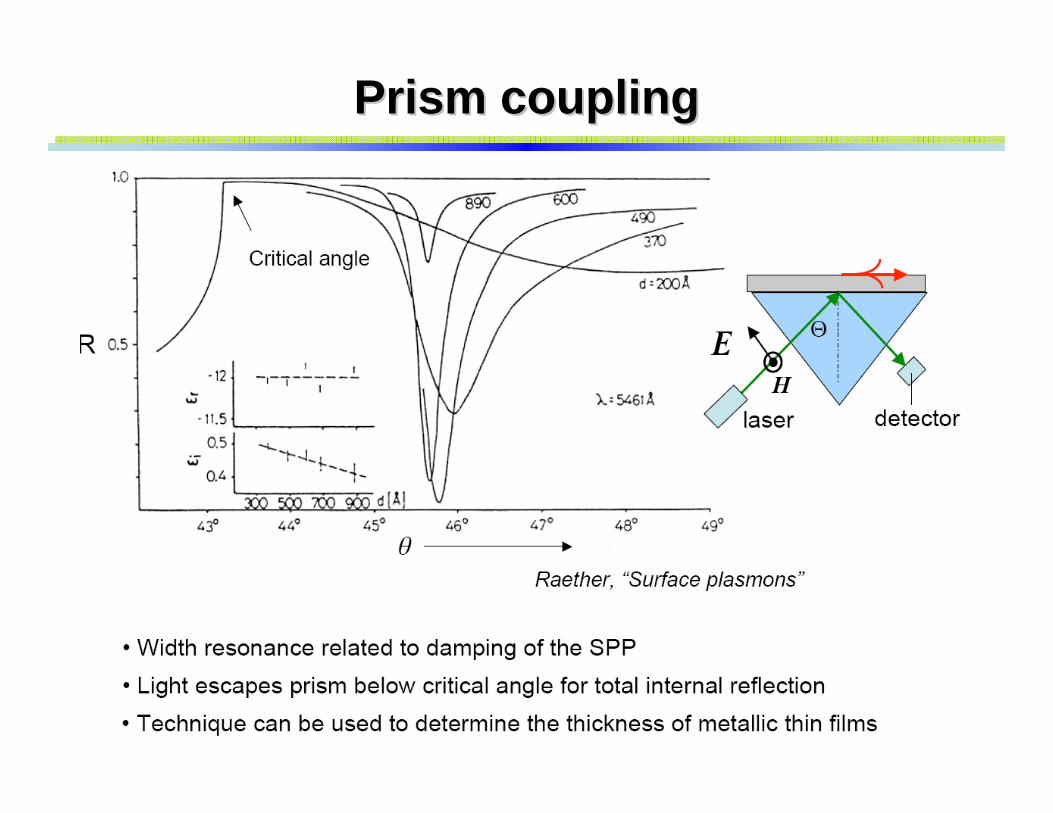
Prism couplingPrism coupling
-40 0 40 80 120 1600.0
0.1
0.2
0.3
0.4
0.5
0.6
Ral
ativ
e A
mpl
itude
Z Direction (nm)
Ez Ex
PRAl
0 1 2 3 4 50.0
0.2
0.4
0.6
Ex Ez
Ampl
itude
(a.u
.)X Direction (μm)
Wavelength: 365nm
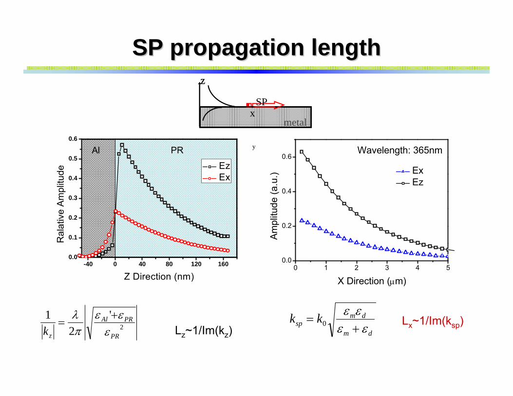
2'
21
PR
PRAl
zk εεε
πλ +
=dm
dmsp kk
εεεε+
= 0Lz~1/Im(kz)
Lx~1/Im(ksp)
SP propagation length SP propagation length
y
metal
SPx
zz

SP coupling between interfaces SP coupling between interfaces
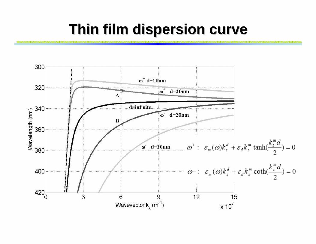
Thin film dispersion curveThin film dispersion curve

Plasmonics at nanoscalePlasmonics at nanoscale
Related Documents


![INVITED PAPER QuantumPlasmonics€¦ · ters near plasmonic structures [20], graphene plasmonics [21], semiconductor plasmonics [22], hot electrons [23], and active quantum plasmonics](https://static.cupdf.com/doc/110x72/5f0859367e708231d4219104/invited-paper-quantumplasmonics-ters-near-plasmonic-structures-20-graphene-plasmonics.jpg)


