Weak mismatch epitaxy and structural feedback in graphene growth on copper foil Neil R. Wilson 1 ( ), Alexander J. Marsden 1 , Mohammed Saghir 1 , Catherine J. Bromley 2 , Renald Schaub 2 , Giovanni Costantini 3 , Thomas W. White 3 , Cerianne Partridge 3 , Alexei Barinov 4 , Pavel Dudin 4 , Ana M. Sanchez 1 , James J. Mudd 1 , Marc Walker 1 , and Gavin R. Bell 1 1 Department of Physics, University of Warwick, Coventry, CV4 7AL, UK 2 EaStCHEM School of Chemistry, University of St Andrews, St Andrews, KY16 9ST, UK 3 Department of Chemistry, University of Warwick, Coventry, CV4 7AL, UK 4 Sincrotrone Trieste S.C.p.A., Area Science Park, I-34012 Basovizza, Trieste, Italy Received: 12 September 2012 Revised: 9 November 2012 Accepted: 3 December 2012 © The Author(s) 2013. This article is published with open access at Springerlink.com KEYWORDS graphene, chemical vapor deposition, mismatch epitaxy, structural feedback, low energy electron diffraction, angle resolved photo-emission spectroscopy (ARPES) ABSTRACT Graphene growth by low-pressure chemical vapor deposition on low cost copper foils shows great promise for large scale applications. It is known that the local crystallography of the foil influences the graphene growth rate. Here we find an epitaxial relationship between graphene and copper foil. Interfacial restructuring between graphene and copper drives the formation of (n10) facets on what is otherwise a mostly Cu(100) surface, and the facets in turn influence the graphene orientations from the onset of growth. Angle resolved photoemission shows that the electronic structure of the graphene is decoupled from the copper indicating a weak interaction between them. Despite this, two preferred orientations of graphene are found, ±8° from the Cu[010] direction, creating a non-uniform distribution of graphene grain boundary misorientation angles. Comparison with the model system of graphene growth on single crystal Cu(110) indicates that this orientational alignment is due to mismatch epitaxy. Despite the differences in symmetry the orientation of the graphene is defined by that of the copper. We expect these observations to not only have importance for controlling and understanding the growth process for graphene on copper, but also to have wider implications for the growth of two-dimensional materials on low cost metal substrates. 1 Introduction Since the first demonstration in 2009 [1], graphene growth by chemical vapor deposition (CVD) on copper foil has become established as one of the most promising routes for the large-scale production of graphene for electronic and opto-electronic applications. Catalytic decomposition of hydrocarbons on a copper Nano Research 2013, 6(2): 99–112 DOI 10.1007/s12274-013-0285-y Address correspondence to [email protected]

Welcome message from author
This document is posted to help you gain knowledge. Please leave a comment to let me know what you think about it! Share it to your friends and learn new things together.
Transcript

Weak mismatch epitaxy and structural feedback in graphene growth on copper foil
Neil R. Wilson1 (), Alexander J. Marsden1, Mohammed Saghir1, Catherine J. Bromley2, Renald Schaub2,
Giovanni Costantini3, Thomas W. White3, Cerianne Partridge3, Alexei Barinov4, Pavel Dudin4, Ana M. Sanchez1,
James J. Mudd1, Marc Walker1, and Gavin R. Bell1
1 Department of Physics, University of Warwick, Coventry, CV4 7AL, UK 2 EaStCHEM School of Chemistry, University of St Andrews, St Andrews, KY16 9ST, UK 3 Department of Chemistry, University of Warwick, Coventry, CV4 7AL, UK 4 Sincrotrone Trieste S.C.p.A., Area Science Park, I-34012 Basovizza, Trieste, Italy
Received: 12 September 2012 Revised: 9 November 2012 Accepted: 3 December 2012 © The Author(s) 2013. This article is published with open access at Springerlink.com KEYWORDS graphene, chemical vapor deposition, mismatch epitaxy, structural feedback, low energy electron diffraction, angle resolved photo-emission spectroscopy (ARPES)
ABSTRACT Graphene growth by low-pressure chemical vapor deposition on low cost copperfoils shows great promise for large scale applications. It is known that the localcrystallography of the foil influences the graphene growth rate. Here we find anepitaxial relationship between graphene and copper foil. Interfacial restructuringbetween graphene and copper drives the formation of (n10) facets on what is otherwise a mostly Cu(100) surface, and the facets in turn influence the grapheneorientations from the onset of growth. Angle resolved photoemission shows thatthe electronic structure of the graphene is decoupled from the copper indicatinga weak interaction between them. Despite this, two preferred orientations ofgraphene are found, ±8° from the Cu[010] direction, creating a non-uniform distribution of graphene grain boundary misorientation angles. Comparisonwith the model system of graphene growth on single crystal Cu(110) indicatesthat this orientational alignment is due to mismatch epitaxy. Despite thedifferences in symmetry the orientation of the graphene is defined by that of thecopper. We expect these observations to not only have importance for controllingand understanding the growth process for graphene on copper, but also to havewider implications for the growth of two-dimensional materials on low cost metal substrates.
1 Introduction
Since the first demonstration in 2009 [1], graphene growth by chemical vapor deposition (CVD) on copper
foil has become established as one of the most promising routes for the large-scale production of graphene for electronic and opto-electronic applications. Catalytic decomposition of hydrocarbons on a copper
Nano Research 2013, 6(2): 99–112 DOI 10.1007/s12274-013-0285-y
Address correspondence to [email protected]

| www.editorialmanager.com/nare/default.asp
100 Nano Res. 2013, 6(2): 99–112
surface can grow graphene self-limited to a monolayer coverage, forming a continuous polycrystalline sheet (an atomic patchwork quilt [2]) with the individual graphene grains joined at grain boundaries [2–6]. The grain boundaries can significantly degrade the otherwise superlative mechanical and electrical properties of CVD grown graphene [6–10]. However, the misorientation angle of the grain boundary (i.e., the relative orientation of the graphene grains either side of the grain boundary) plays an important role in defining its properties. For example, it has been reported that the mechanical strength of the grain boundary can approach that of defect-free graphene for large misorientation angles [9].
Early surface science studies on “monolayer graphite” concentrated on graphene overlayers on transition metals such as Ni, Pt, and Ir. In many cases the (111) surface of the transition metal was used; the triangular lattice of the (111) surface of such face-centered cubic crystals provides a suitable three-fold symmetry match to the graphene lattice, and hence graphene growth can be epitaxial with the crystallographic orientation of the graphene determined by the crystallography of the metal surface [11]. An important question to ask is whether the orientation of graphene grown on copper foil is similarly influenced by the local crystallography of the copper surface.
Recently the graphene growth rate has been shown to be dependent on the crystallographic orientation of the copper grain by using electron backscatter diffraction (EBSD) to determine the grain structure and local crystallography of the foil [12–15], with faster growth rates reported on Cu(111) than Cu(100) [15]. Recent studies have also applied surface science techniques to study the orientation of graphene grown on single crystal copper substrates [16–18], on heteroepitaxial Cu films deposited on sapphire substrates [19, 20], and on copper foil [20, 21]. Wofford et al. used low energy electron microscopy (LEEM) and low energy electron diffraction (LEED, sensitive to the surface crystallography) to study graphene growth on copper foil and, although the graphene was often in registry with the [010] direction of the Cu(100) surface, a range of relative in-plane orientations were observed [21]. Analysis of moiré patterns in STM has also been used to study the orientation of graphene relative to the copper surface [17, 18, 22], whereby
Gao et al. showed that graphene was mostly either aligned with the Cu(111) surface or rotated by 7° [18]. Similarly Zhao et al. found that the graphene grew primarily in registry with the underlying copper lattice for both Cu(111) and Cu(100) [17]. There is clear evidence that the growth mechanism depends on the growth conditions, and those used in all of these ultra-high vacuum (UHV) growth studies were very different from the “standard” conditions used for low-pressure (LP-) CVD. Orofeo et al. have shown that on a heteroepitaxial Cu(111) film, ambient pressure CVD can give graphene well-aligned to the copper substrate [20] but no such orientational relationship has been established for LP-CVD growth of graphene on low cost foil substrates.
In this work we study the effect of substrate topography and orientation on graphene growth under standard LP-CVD conditions on the most industrially relevant substrate, copper foil. We find compelling evidence, across length scales from nm to mm, for preferred orientations of the graphene grains relative to the crystallography of the underlying copper, predominantly near (100) in orientation. There is an apparent structural feedback between the graphene and copper surface, whereby the graphene induces and stabilizes restructuring of the Cu surface to form (n10) facets and in turn these facets play an important role in the nucleation and growth of the graphene. The preferential orientations of the graphene result in a peak in the distribution of graphene grain boundary misorientation angles. By studying graphene grown on the simplest example of a Cu(n10) facet, single crystal Cu(110), we find a clear indication that the preferred orientations are due to mismatch epitaxy of the hexagonal graphene overlayer on the lower symmetry lattice of the copper foil surface. Angle resolved photo-emission spectroscopy (ARPES) within graphene grains on the copper foil shows that epitaxial alignment occurs despite the graphene being only weakly physisorbed onto the copper.
2 Results and discussion
2.1 Copper crystallography and topography after graphene growth
After the growth process, which included a 20 min
www.theNanoResearch.com∣www.Springer.com/journal/12274 | Nano Research
101Nano Res. 2013, 6(2): 99–112
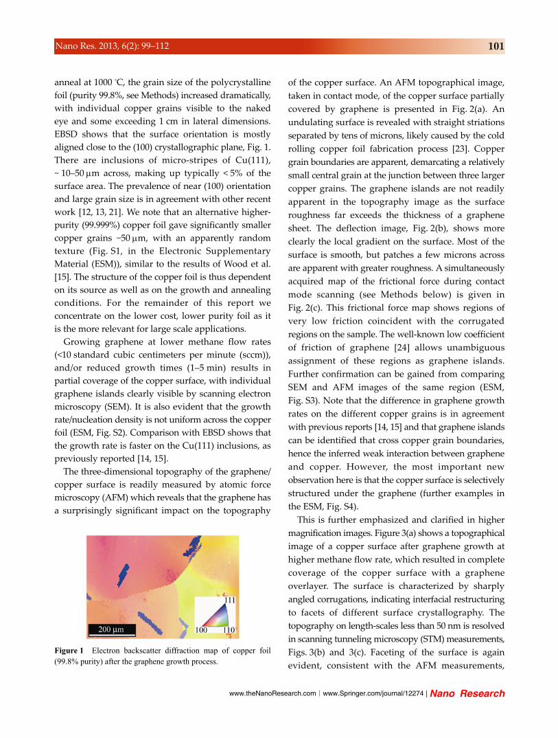
anneal at 1000 °C, the grain size of the polycrystalline foil (purity 99.8%, see Methods) increased dramatically, with individual copper grains visible to the naked eye and some exceeding 1 cm in lateral dimensions. EBSD shows that the surface orientation is mostly aligned close to the (100) crystallographic plane, Fig. 1. There are inclusions of micro-stripes of Cu(111), ~ 10–50 m across, making up typically < 5% of the surface area. The prevalence of near (100) orientation and large grain size is in agreement with other recent work [12, 13, 21]. We note that an alternative higher- purity (99.999%) copper foil gave significantly smaller copper grains ~50 m, with an apparently random texture (Fig. S1, in the Electronic Supplementary Material (ESM)), similar to the results of Wood et al. [15]. The structure of the copper foil is thus dependent on its source as well as on the growth and annealing conditions. For the remainder of this report we concentrate on the lower cost, lower purity foil as it is the more relevant for large scale applications.
Growing graphene at lower methane flow rates (<10 standard cubic centimeters per minute (sccm)), and/or reduced growth times (1–5 min) results in partial coverage of the copper surface, with individual graphene islands clearly visible by scanning electron microscopy (SEM). It is also evident that the growth rate/nucleation density is not uniform across the copper foil (ESM, Fig. S2). Comparison with EBSD shows that the growth rate is faster on the Cu(111) inclusions, as previously reported [14, 15].
The three-dimensional topography of the graphene/ copper surface is readily measured by atomic force microscopy (AFM) which reveals that the graphene has a surprisingly significant impact on the topography
Figure 1 Electron backscatter diffraction map of copper foil (99.8% purity) after the graphene growth process.
of the copper surface. An AFM topographical image, taken in contact mode, of the copper surface partially covered by graphene is presented in Fig. 2(a). An undulating surface is revealed with straight striations separated by tens of microns, likely caused by the cold rolling copper foil fabrication process [23]. Copper grain boundaries are apparent, demarcating a relatively small central grain at the junction between three larger copper grains. The graphene islands are not readily apparent in the topography image as the surface roughness far exceeds the thickness of a graphene sheet. The deflection image, Fig. 2(b), shows more clearly the local gradient on the surface. Most of the surface is smooth, but patches a few microns across are apparent with greater roughness. A simultaneously acquired map of the frictional force during contact mode scanning (see Methods below) is given in Fig. 2(c). This frictional force map shows regions of very low friction coincident with the corrugated regions on the sample. The well-known low coefficient of friction of graphene [24] allows unambiguous assignment of these regions as graphene islands. Further confirmation can be gained from comparing SEM and AFM images of the same region (ESM, Fig. S3). Note that the difference in graphene growth rates on the different copper grains is in agreement with previous reports [14, 15] and that graphene islands can be identified that cross copper grain boundaries, hence the inferred weak interaction between graphene and copper. However, the most important new observation here is that the copper surface is selectively structured under the graphene (further examples in the ESM, Fig. S4).
This is further emphasized and clarified in higher magnification images. Figure 3(a) shows a topographical image of a copper surface after graphene growth at higher methane flow rate, which resulted in complete coverage of the copper surface with a graphene overlayer. The surface is characterized by sharply angled corrugations, indicating interfacial restructuring to facets of different surface crystallography. The topography on length-scales less than 50 nm is resolved in scanning tunneling microscopy (STM) measurements, Figs. 3(b) and 3(c). Faceting of the surface is again evident, consistent with the AFM measurements,

| www.editorialmanager.com/nare/default.asp
102 Nano Res. 2013, 6(2): 99–112
whilst on the facets hexagonal patterns characteristic of graphene are seen, Fig. 3(c). Along with Raman spectroscopy (ESM, Fig. S5) and transmission electron microscopy (TEM, see later), this proves that the majority of the surface is covered by a monolayer of graphene.
Observations of the restructuring of the copper surface under graphene have recently been reported [25], with evidence for periodic surface depressions induced by partial dislocations in the copper covered by graphene. Such periodic depressions were not observed on our samples, but the interfacial reconstruction of the copper under the graphene is clear.
Figures 2 and 3 are taken after growth, and so cannot determine the surface topography as it was whilst the graphene was forming. However, it is known that the copper surface is highly mobile at
the growth temperature [21]. From this we infer that the interfacial restructuring occurs underneath the graphene and hence must be caused and/or stabilized by the presence of the graphene overlayer. To study the surface arrangement of the copper and the relationship between the copper and graphene in more detail, we use LEED which is sensitive to only the top few atomic layers of a sample. LEED is complementary to EBSD in that EBSD probes the near surface crystallography and hence is sensitive to the underlying crystallography of the copper grains but not to the surface rearrangements or graphene overlayer.
2.2 Surface crystallography of copper foil and graphene overlayer
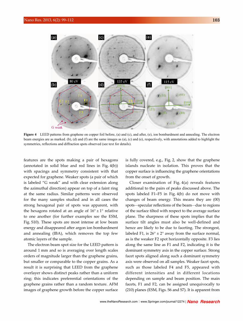
A typical LEED pattern of a copper foil after growth of graphene is shown in Fig. 4(a); the pattern was taken at low beam energy (80 eV). The most striking
Figure 2 AFM of graphene grown on copper foil at sub-monolayer coverage: (a) the topography and (b) the deflection image. A qualitative map of the local friction is given in (c), formed by subtracting the lateral force images in the trace and retrace directions (see Methods).
Figure 3 (a) AFM, (b) and (c) STM topography images of graphene on copper foil. In (c) a hexagonal ball and stick lattice representation of graphene is overlaid in black to indicate the atomic positions. The full height scale in (b) is 3 nm and (c) 0.1 nm.
www.theNanoResearch.com∣www.Springer.com/journal/12274 | Nano Research
103Nano Res. 2013, 6(2): 99–112
features are the spots making a pair of hexagons (annotated in solid blue and red lines in Fig. 4(b)) with spacings and symmetry consistent with that expected for graphene. Weaker spots (a pair of which is labeled “G weak” and with clear extension along the azimuthal direction) appear on top of a faint ring at the same radius. Similar patterns were observed for the many samples studied and in all cases the strong hexagonal pair of spots was apparent, with the hexagons rotated at an angle of 16° ± 1° relative to one another (for further examples see the ESM, Fig. S10). These spots are most intense at low beam energy and disappeared after argon ion bombardment and annealing (IBA), which removes the top few atomic layers of the sample.
The electron beam spot size for the LEED pattern is around 1 mm and so is averaging over length scales orders of magnitude larger than the graphene grains, but smaller or comparable to the copper grains. As a result it is surprising that LEED from the graphene overlayer shows distinct peaks rather than a uniform ring; this indicates preferential orientations of the graphene grains rather than a random texture. AFM images of graphene growth before the copper surface
is fully covered, e.g., Fig. 2, show that the graphene islands nucleate in isolation. This proves that the copper surface is influencing the graphene orientations from the onset of growth.
Closer examination of Fig. 4(a) reveals features additional to the pairs of peaks discussed above. The spots labeled F1–F5 in Fig. 4(b) do not move with changes of beam energy. This means they are (00) spots—specular reflections of the beam—due to regions of the surface tilted with respect to the average surface plane. The sharpness of these spots implies that the surface tilt angles must also be well-defined and hence are likely to be due to faceting. The strongest, labeled F1, is 26° ± 2° away from the surface normal, as is the weaker F2 spot horizontally opposite. F3 lies along the same line as F1 and F2, indicating it is the dominant symmetry axis in the copper surface. Strong facet spots aligned along such a dominant symmetry axis were observed on all samples. Weaker facet spots, such as those labeled F4 and F5, appeared with different intensities and in different locations depending on sample and beam position. The main facets, F1 and F2, can be assigned unequivocally to (210) planes (ESM, Figs. S6 and S7). It is apparent from
Figure 4 LEED patterns from graphene on copper foil before, (a) and (c), and after, (e), ion bombardment and annealing. The electron beam energies are as marked. (b), (d) and (f) are the same images as (a), (c) and (e), respectively, with annotations added to highlight the symmetries, reflections and diffraction spots observed (see text for details).
| www.editorialmanager.com/nare/default.asp
104 Nano Res. 2013, 6(2): 99–112
examination of LEED patterns at varying electron beam energy that there are diffraction peaks centered on F1 (see the video in the ESM). The most prominent are those associated with graphene (labeled by the sections of dashed hexagons in Fig. 4(b)) and these have the same orientational relationship to the dominant symmetry axis as the main graphene spots, indicating that the copper substrate facets are large (on the atomic scale) and the graphene is continuous across them. Further details about the LEED patterns and their indexing are given in the ESM, Figs. S8, S9 and S10.
Crucially, LEED allows the registry between the substrate and graphene overlayer to be examined directly. The LEED patterns appear significantly more complicated at higher beam energies, where more Cu substrate spots appear. A typical pattern at 135 eV is shown in Fig. 4(c). The dominant symmetry axis is the [010] direction, labeled by the horizontal solid green line in Fig. 4(d), on which most of the facet reflections appear. The parallel dashed lines highlight rows of Cu spots whose spacing is consistent with (n10) and (100) spots, as would be expected on the predominantly Cu(100) surface with facets in the [010] direction. It is clear that the graphene and substrate diffraction features are mutually aligned, sharing a two-fold symmetry, i.e., the graphene is oriented with respect to the dominant symmetry axis of the faceted copper surface.
Subjecting graphene on copper foil to cycles of ion bombardment and annealing (IBA) in UHV (as typically used to clean single crystal samples), resulted in LEED patterns consistently similar to the one shown in Fig. 4(e). The square pattern is easily indexed to Cu(100). After IBA, AFM measurements show a locally smooth, facet-free surface (ESM, Fig. S11). This confirms that the surface reconstruction of the copper is caused and stabilized by the graphene.
In summary, AFM, STM and LEED indicate interfacial restructuring of the copper surface under the graphene, resulting in pronounced faceting mostly from Cu(100) to Cu(n10). Note that this suggests caution should be taken in studying the crystallographic dependence of graphene growth by EBSD alone; EBSD has a depth sensitivity of ~10–100 nm and so
does not give information about the kind of surface rearrangements observed here by LEED (which is only sensitive to the top few atomic layers). As a result EBSD and LEED are highly complementary. LEED detects not only the copper crystallography, but also the macroscopically averaged graphene orientations and here shows that graphene predominately adopts two preferred orientations ±8° from the Cu[010]. For epitaxially oriented growth of graphene on a square lattice like the fcc metal (100) surface, one would expect to see four orientations each having equivalent registry to the (100) surface (i.e., reflected about [010] and [001] surface mirror axes). The two orientations dominantly observed here indicate that the symmetry is broken. This is likely to be caused by the surface restructuring: (n10) facets have rectangular rather than square unit cells. The effect of this mismatch in symmetry between graphene and copper surface is discussed later.
2.3 Microscopic analysis of graphene grain structure
In order to investigate the effect of the preferential orientations of graphene on the grain boundary misorientation angles, it is necessary to measure the orientations of individual graphene grains. Recently it has been demonstrated that these can be directly visualized by TEM [2–4], although to do so the graphene must be removed from the copper substrate and hence information on the surface crystallography of the copper, and the graphene/copper registry, is lost. Figure 5(a) shows a bright-field TEM image of CVD grown graphene suspended on a lacy carbon support (darker grey contrast). The graphene membrane is clearly continuous, but the bright field image does not distinguish between the individual graphene grains. High resolution TEM (HR-TEM), as shown in Fig. 5(d), resolves the graphene lattice, but it is not practical to acquire atomically resolved HR- TEM images over the length scales (> 1 m) required to analyze complete graphene grains. Selected area electron diffraction (SAED) patterns from each of the two regions that make up the bright-field image are shown in Figs. 5(b) and 5(c). The SAED patterns are similar and in each two superimposed hexagonal patterns can be seen, indicating that two different
www.theNanoResearch.com∣www.Springer.com/journal/12274 | Nano Research
105Nano Res. 2013, 6(2): 99–112
Figure 5 (a) Bright-field TEM image of graphene transferred to a lacy carbon TEM grid; the image is composed of two separate images stitched together. The black borders show the edges of the circular apertures used for the SAED patterns given in (b) and (c). The red and blue hexagons in (b) highlight the two orientations of graphene present. (d) HR-TEM of a suspended graphene sheet.
orientations of graphene are within each aperture, i.e., both SAED patterns are consistent with the presence of at least two misoriented graphene grains.
Dark-field TEM (DFTEM) has been used to directly visualize grains within a polycrystalline graphene film, and when combined with SAED can be used to measure the misorientation angles at the grain boundaries [2–4]. DFTEM forms an image selectively from the electrons diffracted through a given diffraction spot. DFTEM images of the same area taken from different diffraction spots can be merged to form a composite image, where the intensity of a given color gives the intensity of a given diffraction peak for that spatial area (ESM, Fig. S12).
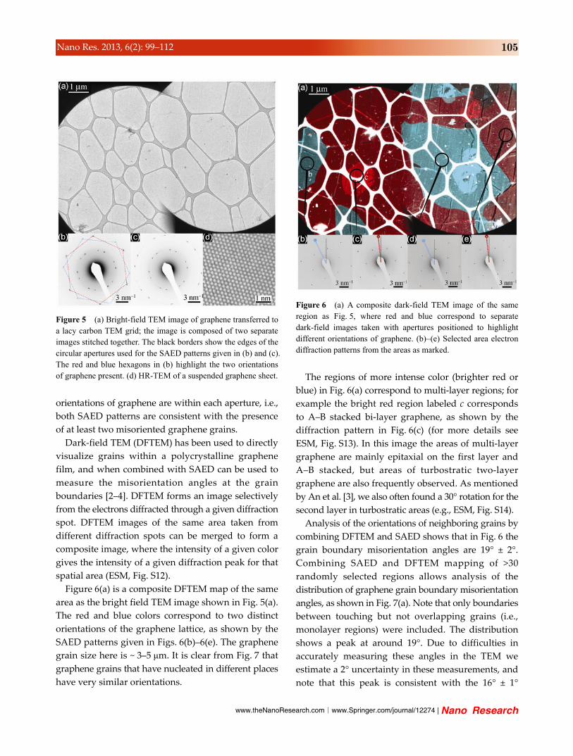
Figure 6(a) is a composite DFTEM map of the same area as the bright field TEM image shown in Fig. 5(a). The red and blue colors correspond to two distinct orientations of the graphene lattice, as shown by the SAED patterns given in Figs. 6(b)–6(e). The graphene grain size here is ~ 3–5 μm. It is clear from Fig. 7 that graphene grains that have nucleated in different places have very similar orientations.
Figure 6 (a) A composite dark-field TEM image of the same region as Fig. 5, where red and blue correspond to separate dark-field images taken with apertures positioned to highlight different orientations of graphene. (b)–(e) Selected area electron diffraction patterns from the areas as marked.
The regions of more intense color (brighter red or blue) in Fig. 6(a) correspond to multi-layer regions; for example the bright red region labeled c corresponds to A–B stacked bi-layer graphene, as shown by the diffraction pattern in Fig. 6(c) (for more details see ESM, Fig. S13). In this image the areas of multi-layer graphene are mainly epitaxial on the first layer and A–B stacked, but areas of turbostratic two-layer graphene are also frequently observed. As mentioned by An et al. [3], we also often found a 30° rotation for the second layer in turbostratic areas (e.g., ESM, Fig. S14).
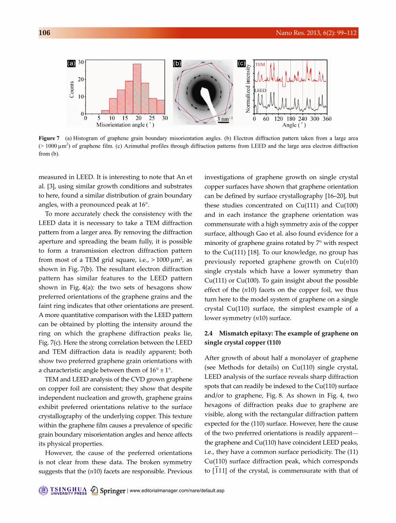
Analysis of the orientations of neighboring grains by combining DFTEM and SAED shows that in Fig. 6 the grain boundary misorientation angles are 19° ± 2°. Combining SAED and DFTEM mapping of >30 randomly selected regions allows analysis of the distribution of graphene grain boundary misorientation angles, as shown in Fig. 7(a). Note that only boundaries between touching but not overlapping grains (i.e., monolayer regions) were included. The distribution shows a peak at around 19°. Due to difficulties in accurately measuring these angles in the TEM we estimate a 2° uncertainty in these measurements, and note that this peak is consistent with the 16° ± 1°
| www.editorialmanager.com/nare/default.asp
106 Nano Res. 2013, 6(2): 99–112
measured in LEED. It is interesting to note that An et al. [3], using similar growth conditions and substrates to here, found a similar distribution of grain boundary angles, with a pronounced peak at 16°.
To more accurately check the consistency with the LEED data it is necessary to take a TEM diffraction pattern from a larger area. By removing the diffraction aperture and spreading the beam fully, it is possible to form a transmission electron diffraction pattern from most of a TEM grid square, i.e., > 1000 m2, as shown in Fig. 7(b). The resultant electron diffraction pattern has similar features to the LEED pattern shown in Fig. 4(a): the two sets of hexagons show preferred orientations of the graphene grains and the faint ring indicates that other orientations are present. A more quantitative comparison with the LEED pattern can be obtained by plotting the intensity around the ring on which the graphene diffraction peaks lie, Fig. 7(c). Here the strong correlation between the LEED and TEM diffraction data is readily apparent; both show two preferred graphene grain orientations with a characteristic angle between them of 16° ± 1°.
TEM and LEED analysis of the CVD grown graphene on copper foil are consistent; they show that despite independent nucleation and growth, graphene grains exhibit preferred orientations relative to the surface crystallography of the underlying copper. This texture within the graphene film causes a prevalence of specific grain boundary misorientation angles and hence affects its physical properties.
However, the cause of the preferred orientations is not clear from these data. The broken symmetry suggests that the (n10) facets are responsible. Previous
investigations of graphene growth on single crystal copper surfaces have shown that graphene orientation can be defined by surface crystallography [16–20], but these studies concentrated on Cu(111) and Cu(100) and in each instance the graphene orientation was commensurate with a high symmetry axis of the copper surface, although Gao et al. also found evidence for a minority of graphene grains rotated by 7° with respect to the Cu(111) [18]. To our knowledge, no group has previously reported graphene growth on Cu(n10) single crystals which have a lower symmetry than Cu(111) or Cu(100). To gain insight about the possible effect of the (n10) facets on the copper foil, we thus turn here to the model system of graphene on a single crystal Cu(110) surface, the simplest example of a lower symmetry (n10) surface.
2.4 Mismatch epitaxy: The example of graphene on single crystal copper (110)
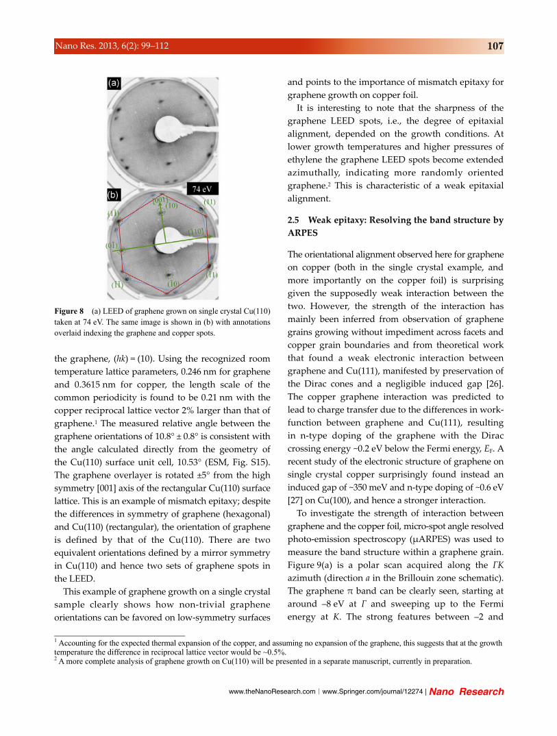
After growth of about half a monolayer of graphene (see Methods for details) on Cu(110) single crystal, LEED analysis of the surface reveals sharp diffraction spots that can readily be indexed to the Cu(110) surface and/or to graphene, Fig. 8. As shown in Fig. 4, two hexagons of diffraction peaks due to graphene are visible, along with the rectangular diffraction pattern expected for the (110) surface. However, here the cause of the two preferred orientations is readily apparent—
the graphene and Cu(110) have coincident LEED peaks, i.e., they have a common surface periodicity. The (11) Cu(110) surface diffraction peak, which corresponds to [111] of the crystal, is commensurate with that of
Figure 7 (a) Histogram of graphene grain boundary misorientation angles. (b) Electron diffraction pattern taken from a large area (> 1000 m2) of graphene film. (c) Azimuthal profiles through diffraction patterns from LEED and the large area electron diffractionfrom (b).
www.theNanoResearch.com∣www.Springer.com/journal/12274 | Nano Research
107Nano Res. 2013, 6(2): 99–112
Figure 8 (a) LEED of graphene grown on single crystal Cu(110) taken at 74 eV. The same image is shown in (b) with annotations overlaid indexing the graphene and copper spots.
the graphene, (hk) = (10). Using the recognized room temperature lattice parameters, 0.246 nm for graphene and 0.3615 nm for copper, the length scale of the common periodicity is found to be 0.21 nm with the copper reciprocal lattice vector 2% larger than that of graphene.1 The measured relative angle between the graphene orientations of 10.8° ± 0.8° is consistent with the angle calculated directly from the geometry of the Cu(110) surface unit cell, 10.53° (ESM, Fig. S15). The graphene overlayer is rotated ±5° from the high symmetry [001] axis of the rectangular Cu(110) surface lattice. This is an example of mismatch epitaxy; despite the differences in symmetry of graphene (hexagonal) and Cu(110) (rectangular), the orientation of graphene is defined by that of the Cu(110). There are two equivalent orientations defined by a mirror symmetry in Cu(110) and hence two sets of graphene spots in the LEED.
This example of graphene growth on a single crystal sample clearly shows how non-trivial graphene orientations can be favored on low-symmetry surfaces
and points to the importance of mismatch epitaxy for graphene growth on copper foil.
It is interesting to note that the sharpness of the graphene LEED spots, i.e., the degree of epitaxial alignment, depended on the growth conditions. At lower growth temperatures and higher pressures of ethylene the graphene LEED spots become extended azimuthally, indicating more randomly oriented graphene.2 This is characteristic of a weak epitaxial alignment.
2.5 Weak epitaxy: Resolving the band structure by ARPES
The orientational alignment observed here for graphene on copper (both in the single crystal example, and more importantly on the copper foil) is surprising given the supposedly weak interaction between the two. However, the strength of the interaction has mainly been inferred from observation of graphene grains growing without impediment across facets and copper grain boundaries and from theoretical work that found a weak electronic interaction between graphene and Cu(111), manifested by preservation of the Dirac cones and a negligible induced gap [26]. The copper graphene interaction was predicted to lead to charge transfer due to the differences in work- function between graphene and Cu(111), resulting in n-type doping of the graphene with the Dirac crossing energy ~0.2 eV below the Fermi energy, EF. A recent study of the electronic structure of graphene on single crystal copper surprisingly found instead an induced gap of ~350 meV and n-type doping of ~0.6 eV [27] on Cu(100), and hence a stronger interaction.
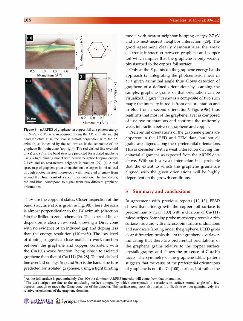
To investigate the strength of interaction between graphene and the copper foil, micro-spot angle resolved photo-emission spectroscopy (µARPES) was used to measure the band structure within a graphene grain. Figure 9(a) is a polar scan acquired along the ΓK azimuth (direction a in the Brillouin zone schematic). The graphene π band can be clearly seen, starting at around –8 eV at Γ and sweeping up to the Fermi energy at K. The strong features between –2 and
1 Accounting for the expected thermal expansion of the copper, and assuming no expansion of the graphene, this suggests that at the growthtemperature the difference in reciprocal lattice vector would be ~0.5%. 2 A more complete analysis of graphene growth on Cu(110) will be presented in a separate manuscript, currently in preparation.
| www.editorialmanager.com/nare/default.asp
108 Nano Res. 2013, 6(2): 99–112
Figure 9 µARPES of graphene on copper foil at a photon energy of 74 eV. (a) Polar scan acquired along the ΓK azimuth and (b) band structure at K, the scan is almost perpendicular to the ΓK azimuth, as indicated by the red arrows in the schematic of the graphene Brillouin zone (top right). The red dashed line overlaid on (a) and (b) is the band structure predicted for isolated graphene using a tight binding model with nearest neighbor hopping energy 2.7 eV and no next-nearest neighbor interaction [29]. (c) A real space map of graphene grain orientation on the copper foil visualized through photoemission microscopy with integrated intensity from around the Dirac point of a specific orientation. The two colors, red and blue, correspond to signal from two different graphene orientations.
–4 eV are the copper d states. Closer inspection of the band structure at K is given in Fig. 9(b); here the scan is almost perpendicular to the ΓK azimuth (direction b in the Brillouin zone schematic). The expected linear dispersion is clearly resolved, showing a Dirac cone with no evidence of an induced gap and doping less than the energy resolution (110 meV). The low level of doping suggests a close match in work-function between the graphene and copper, consistent with the Cu(100) work function1 being closer to isolated graphene than that of Cu(111) [26, 28]. The red dashed line overlaid on Figs. 9(a) and 9(b) is the band structure predicted for isolated graphene, using a tight binding
model with nearest neighbor hopping energy 2.7 eV and no next-nearest neighbor interaction [29]. The good agreement clearly demonstrates the weak electronic interaction between graphene and copper foil which implies that the graphene is only weakly physisorbed to the copper foil surface.
Only at the K points do the graphene energy bands approach EF. Integrating the photoemission near EF at a given azimuthal angle thus allows detection of graphene of a defined orientation; by scanning the sample, graphene grains of that orientation can be visualized. Figure 9(c) shows a composite of two such maps; the intensity in red is from one orientation and in blue from a second orientation2. Figure 9(c) thus reaffirms that most of the graphene layer is composed of just two orientations and confirms the uniformly weak interaction between graphene and copper.
Preferential orientations of the graphene grains are apparent in the LEED and TEM data, but not all grains are aligned along these preferential orientations. This is consistent with a weak interaction driving this epitaxial alignment, as expected from the ARPES data above. With such a weak interaction it is probable that the extent to which the graphene grains are aligned with the given orientations will be highly dependent on the growth conditions.
3 Summary and conclusions
In agreement with previous reports [12, 13], EBSD shows that after growth the copper foil surface is predominantly near (100) with inclusions of Cu(111) micro-stripes. Scanning probe microscopy reveals a rich surface structure with microscopic surface undulations and nanoscale faceting under the graphene. LEED gives clear diffraction peaks due to the graphene overlayer, indicating that there are preferential orientations of the graphene grains relative to the copper surface crystallography, and shows the presence of Cu(n10) facets. The symmetry of the graphene LEED pattern suggests that the cause of the preferential orientations of graphene is not the Cu(100) surface, but rather the
1 As the foil surface is predominantly Cu(100) the dominant ARPES intensity will come from that orientation. 2 The dark stripes are due to the undulating surface topography which corresponds to variations in surface normal angle of a few degrees, enough to move the Dirac cone out of the detector. This surface roughness also makes it difficult to extract quantitatively therelative orientations of the graphene domains.
www.theNanoResearch.com∣www.Springer.com/journal/12274 | Nano Research
109Nano Res. 2013, 6(2): 99–112
facets. There is thus structural feedback between the graphene and copper: the graphene growth induces and stabilizes faceting of the copper surface, and the facets in turn play an important role in the graphene growth mechanism.
Analysis of a model system, graphene growth on single crystal Cu(110) under UHV, presents a strikingly similar result with two graphene orientations on a rectangular Cu(110) surface lattice. The extent of the alignment depends on the growth conditions, with greater alignment observed at higher temperatures. Here, the epitaxial arrangement can clearly be attributed to a common periodicity which results in mismatch epitaxy of the hexagonal graphene on the rectangular crystal surface.
µARPES shows a weak electronic interaction with the graphene physisorbed to the copper foil surface and essentially decoupled from it. This makes the observed dependence of graphene grain orientation on copper crystallography all the more surprising. But the preferential orientations are also observed in TEM investigations of the microscopic graphene grain structure, and lead to a peak in the distribution of grain boundary misorientation angles consistent with the LEED patterns.
Our results lead to the conclusion that graphene growth on copper foil displays structural feedback and weak mismatch epitaxy.
Structural feedback is not a new concept. For example, it has previously been observed in calcite crystallization on self-assembled monolayers (SAM) [30], in the growth of ionic solids on copper surfaces [31], and the adsorption of C60 on Ni(110) [32]. It usually requires a strong interaction between the surface and adsorbate; in the metal surfaces this overcomes the energy required to break the surface bonds during restructuring, and in the SAM it drives the complementary nucleation of a crystalline phase in the fluid SAM below the crystallizing calcite. Here, the copper surface at the graphene growth temperature is extremely fluid, but the apparent weak interaction makes the restructuring remarkable. We suggest two possible explanations: (1) the weak interaction is sufficient due to the extremely fluid copper surface, or (2) there is a strong interaction during the onset of growth, presumably due to the non-planar graphene
nuclei, which drives the surface restructuring. Should the graphene–copper foil relationship be
described as “epitaxial”? The single crystal Cu(110) results clearly show an epitaxial arrangement defined by a common periodicity. However, comparison between the structure of graphene and Cu(100) or Cu(210) shows no obvious lattice vectors or reciprocal lattice vectors that are commensurate and would give the observed ±8° for graphene relative to Cu[010]. Instead of classical epitaxial alignment of infinite crystal lattices, the problem may be more akin to preferential orientational alignment of extended molecules on crystal surfaces. Yakobson and Ding suggested that the sp2-nuclei of graphene are likely to prefer orientations that are not necessarily the same as extended graphene sheets [5], as illustrated in their density functional theory study of graphene nucleation on Ni(111) [33]. Understanding the process here is made more complicated by the observation of structural feedback. Hence, without further theoretical work, it is not clear what mechanism is operating to orientationally pin the graphene to the copper, particularly given the weak interaction observed here between graphene and copper. However, since the dominant graphene orientation is defined by the copper surface orientation we can conclude that there is an epitaxial alignment between the two. The difference in symmetry between the copper surface and graphene means that it is mismatch epitaxy which, as the growth on single crystal Cu(110) shows, can result in non-trivial orientational alignments. The weak interaction, as observed by ARPES, means that the extent of epitaxial alignment will depend on growth conditions. Note also that we do not expect the observed orientations (±8° for graphene relative to Cu[010]) to be generic across all types of copper foil, but we do expect that the effects of weak mismatch epitaxy and structural feedback will be.
These results demonstrate the importance of the copper surface crystallography to the nucleation and growth of graphene, and in particular point to the importance of heterogeneities such as facets in defining the growth mechanisms. Our results suggest that the epitaxial alignment of graphene could be controlled by crystallographic engineering of the copper, even on relatively low cost, mass produced
| www.editorialmanager.com/nare/default.asp
110 Nano Res. 2013, 6(2): 99–112
copper foil. More generally, we expect structural feedback and mismatch epitaxy to play important roles in the growth of two-dimensional materials on metal surfaces.
4 Methods
4.1 Graphene growth on copper foil
Copper foil (99.5% purity, 0.025 mm thick, Alfa Aesar product number 13382 or 99.999% purity, 0.025 mm thick, Alfa Aesar product number 10950) was placed in a 1 inch diameter tube furnace and heated to 1000 °C at a rate of 15 °C/min, annealed for 20 min, exposed to methane (purity 99.95%), and then allowed to cool, with at all times a flow of 2 sccm hydrogen (pressure 6 × 10⁻² mbar, purity 99.999%). Growth times varied between 1 and 20 min (typically 10 min) with typical methane flow rates of 35 sccm (total pressure 8 × 10⁻¹ mbar).
4.2 Graphene growth on single crystal Cu(110)
A Cu(110) single crystal was prepared in an ultra-high- vacuum environment, with a base pressure below 10–10 mbar, by multiple IBA cycles (Ar+, 1.5 keV, 10 min at 300 K followed by 15 min anneal at 770 K). The presence of a clean surface was confirmed by LEED and STM measurements, revealing large terraces separated by solely mono-atomic steps. Graphene growth was achieved by following a previously reported methodology [18], whereby the Cu(110) surface is exposed to 10–6 mbar of ethylene while its temperature was ramped up and down between 300 K and 1000 K (approximately 30 minutes per cycle). The cooling down of the sample to 300 K in the last cycle was performed in an evacuated system. STM measurements (not shown here) indicated that the graphene coverage was roughly proportional to the number of cycles, and 10 cycles are enough to yield exclusively single domain graphene islands with sizes ranging up to few 100 nm in diameter.
4.3 Characterisation
AFM and frictional force microscopy were performed on an Asylum Research MFP3D-SA. By scanning the
AFM tip perpendicular to the AFM cantilever axis, changes in the frictional force between the tip and surface cause the cantilever to twist, a lateral force. This lateral force is dependent on the local topography, however, by subtracting the force from scanning in opposite directions (trace and retrace), a qualitative measure of the local friction can be gained as presented in Fig. 2(c). STM images on copper foil were acquired under ambient conditions with a Veeco STM with Nanoscope E controller and an A-type scanner, using mechanically-sheared Pt/Ir tips, a negative bias of ~–50 meV applied to the sample (i.e., filled state imaging) and tunneling currents of ~1 nA.
SEM and EBSD were acquired on a Zeiss Supra 55-VP field emission SEM with an EDAX EBSD System. EBSD is sensitive to the top 10–100 nm of the sample (and so does not resolve the graphene overlayer on the copper surface), and has spatial resolution of <100 nm. LEED is sensitive to just the top few atomic layers (including both the graphene and the copper surface). The spot size in conventional LEED systems such as those used here is typically around 1 mm. As a result LEED and EBSD are complementary tools.
LEED experiments on copper foil samples were performed in UHV using an electron energy in the range 25–250 eV. Prior to investigation, Cu foil samples were prepared in UHV by degassing to 300 °C for 30 min. The highly effective passivation of the Cu surface by the graphene layer means that even such gentle cleaning treatment is sufficient to reveal a clear LEED pattern. We show contrast-optimised patterns in the main figures: original data are given in the video in the ESM.
For TEM analysis, the graphene was transferred from the copper growth substrate to a lacy carbon support grid. A bilayer of methylmethacrylate (MMA)/poly methylmethacrylate (PMMA) film was spin coated on the graphene on copper substrate, and the copper removed by a copper etchant (FeCl3, Alfa Aesar 44583). After etching, the stack of graphene on MMA/PMMA was repeatedly washed by transferring to deionised water. A lacy carbon TEM grid (on 400 mesh copper grid) was then placed on top of the stack, lifted from the deionized water on a piece of paper, and dried in a vacuum oven at 60 °C for 30 min. Finally the MMA/PMMA was removed by gentle soaking in
www.theNanoResearch.com∣www.Springer.com/journal/12274 | Nano Research
111Nano Res. 2013, 6(2): 99–112
acetone for 90 min, and the resultant graphene TEM grid dried in a vacuum oven at 60 °C for 30 min. Conventional TEM and dark-field TEM were per- formed on a Jeol 2000FX operated at 200 kV with a Gatan Orius camera. High resolution TEM images were acquired on a Jeol ARM200F TEM/STEM with dual aberration correction, operated at 80 kV.
LEED and STM measurements on a single-crystal Cu(110) surface were performed in a UHV chamber with base pressure better than 10–10 mbar. Electron energies for LEED ranged from 50 to 200 eV. All STM measurements (low-temperature CreaTec instrument, Germany) were acquired with positive bias applied to the sample kept at 77 K by liquid nitrogen cryo- cooling of the STM block. Voltages used varied from a few mV to about 1 V, with tunneling currents of ~100 pA.
µARPES was performed at the spectromicroscopy beam line at the Elettra synchrotron light source using 74 eV light focused to a submicrometer spot [34]. The sample was at room temperature during measurements. Lateral, total energy and angular resolutions were ~1 µm, 110 meV and ±0.3o respectively.
Acknowledgments
We thank M. Papagno, D. P. Woodruff, N. V. Richardson, and R. Beanland for helpful discussions and S. York for technical support. We thank the EPSRC for support through the ULISSE grant (EP/G044864/1) and a studentship for AMS. AMS and NRW acknowledge support from the Warwick Centre for Analytical Science (EP/F034210/1). Equipment used in this research was funded by Birmingham Science City: Creating and Characterising Next Generation Advanced Materials, with support from Advantage West Midlands and partly funded by the European Regional Development Fund.
Electronic Supplementary Material: Supplementary Material (Raman spectroscopy, AFM, EBSD, LEED and TEM and a movie showing LEED as a function of beam energy for graphene on copper foil) is available in the online version of this article at http://dx.doi.org/10.1007/s12274-013-0285-y.
Open Access: This article is distributed under the terms of the Creative Commons Attribution Noncommercial License which permits any noncommercial use, distri- bution, and reproduction in any medium, provided the original author(s) and source are credited.
References
[1] Li, X.; Cai, W.; An, J.; Kim, S.; Nah, J.; Yang, D.; Piner, R.;
Velamakanni, A.; Jung, I.; Tutuc, E.; et al. Large-area synthesis
of high-quality and uniform graphene films on copper foils.
Science 2009, 324, 1312–1314.
[2] Huang, P. Y.; Ruiz-Vargas, C. S.; van der Zande, A. M.;
Whitney, W. S.; Levendorf, M. P.; Kevek, J. W.; Garg, S.;
Alden, J. S.; Hustedt, C. J.; Zhu, Y.; et al. Grains and grain
boundaries in single-layer graphene atomic patchwork quilts.
Nature 2011, 469, 389–392.
[3] An, J.; Voelkl, E.; Suk, J. W.; Li, X.; Magnuson, C. W.; Fu,
L.; Tiemeijer, P.; Bischoff, M.; Freitag, B.; Popova, E.; et al.
Domain (grain) boundaries and evidence of “twinlike”
structures in chemically vapor deposited grown graphene.
ACS Nano 2011, 5, 2433–2439.
[4] Kim, K.; Lee, Z.; Regan, W.; Kisielowski, C.; Crommie, M.
F.; Zettl, A. Grain boundary mapping in polycrystalline
graphene. ACS Nano 2011, 5, 2142–2146.
[5] Yakobson, B. I.; Ding, F. Observational geology of graphene,
at the nanoscale. ACS Nano 2011, 5, 1569–1574.
[6] Yu, Q.; Jauregui, L. A.; Wu, W.; Colby, R.; Tian, J.; Su, Z.;
Cao, H.; Liu, Z.; Pandey, D.; Wei, D.; et al. Control and
characterization of individual grains and grain boundaries in
graphene grown by chemical vapour deposition. Nat. Mater.
2011, 10, 443–449.
[7] Malola, S.; Häkkinen, H.; Koskinen, P. Structural, chemical,
and dynamical trends in graphene grain boundaries. Phys.
Rev. B 2010, 81, 165447.
[8] Zhang, J.; Zhao, J.; Lu, J. Intrinsic strength and failure
behaviors of graphene grain boundaries. ACS Nano 2012, 6,
2704–2711.
[9] Grantab, R.; Shenoy, V. B.; Ruoff, R. S. Anomalous strength
characteristics of tilt grain boundaries in graphene. Science
2010, 330, 946–948.
[10] Kumar, S. B.; Guo, J. Strain-induced conductance modulation
in graphene grain boundary. Nano Lett. 2012, 12, 1362–1366.
[11] Wintterlin, J.; Bocquet, M. L. Graphene on metal surfaces.
Surf. Sci. 2009, 603, 1841–1852.
[12] Robinson, Z. R.; Tyagi, P.; Murray, T. M.; Ventrice, C. A.;
Chen, S.; Munson, A.; Magnuson, C. W.; Ruoff, R. S.
Substrate grain size and orientation of Cu and Cu–Ni foils
used for the growth of graphene films. J. Vac. Sci. Technol.
A 2012, 30, 011401.
| www.editorialmanager.com/nare/default.asp
112 Nano Res. 2013, 6(2): 99–112
[13] Chen, S.; Cai, W.; Piner, R. D.; Suk, J. W.; Wu, Y.; Ren, Y.;
Kang, J.; Ruoff, R. S. Synthesis and characterization of large-
area graphene and graphite films on commercial Cu–Ni alloy
foils. Nano Lett. 2011, 11, 3519–3525.
[14] Ishihara, M.; Koga, Y.; Kim, J.; Tsugawa, K.; Hasegawa,
M. Direct evidence of advantage of Cu(111) for graphene
synthesis by using Raman mapping and electron backscatter
diffraction. Mater. Lett. 2011, 65, 2864–2867.
[15] Wood, J. D.; Schmucker, S. W.; Lyons, A. S.; Pop, E.;
Lyding, J. W. Effects of polycrystalline Cu substrate on
graphene growth by chemical vapor deposition. Nano Lett.
2011, 11, 4547–4554.
[16] Nie, S.; Wofford, J. M.; Bartelt, N. C.; Dubon, O. D.;
McCarty, K. F. Origin of the mosaicity in graphene grown
on Cu(111). Phys. Rev. B 2011, 84, 155425.
[17] Zhao, L.; Rim, K. T.; Zhou, H.; He, R.; Heinz, T. F.; Pinczuk,
A.; Flynn, G. W.; Pasupathy, A. N. Influence of copper
crystal surface on the CVD growth of large area monolayer
graphene. Solid State Commun. 2011, 151, 509–513.
[18] Gao, L.; Guest, J. R.; Guisinger, N. P. Epitaxial graphene
on Cu(111). Nano Lett. 2010, 10, 3512–3516.
[19] Ogawa, Y.; Hu, B.; Orofeo, C. M.; Tsuji, M.; Ikeda, K.-I.;
Mizuno, S.; Hibino, H.; Ago, H. Domain structure and
boundary in single-layer graphene grown on Cu(111) and
Cu(100) Films. J. Phys. Chem. Lett. 2011, 3, 219–226.
[20] Orofeo, C. M.; Hibino, H.; Kawahara, K.; Ogawa, Y.; Tsuji,
M.; Ikeda, K.-I.; Mizuno, S.; Ago, H. Influence of Cu metal
on the domain structure and carrier mobility in single-layer
graphene. Carbon 2012, 50, 2189–2196.
[21] Wofford, J. M.; Nie, S.; McCarty, K. F.; Bartelt, N. C.;
Dubon, O. D. Graphene islands on Cu foils: The interplay
between shape, orientation, and defects. Nano Lett. 2010,
10, 4890–4896.
[22] Rasool, H. I.; Song, E. B.; Allen, M. J.; Wassei, J. K.;
Kaner, R. B.; Wang, K. L.; Weiller, B. H.; Gimzewski, J. K.
Continuity of graphene on polycrystalline copper. Nano Lett.
2010, 11, 251–256.
[23] Zhang, B.; Lee, W. H.; Piner, R.; Kholmanov, I.; Wu, Y.; Li,
H.; Ji, H.; Ruoff, R. S. Low-temperature chemical vapor
deposition growth of graphene from toluene on electropolished
copper foils. ACS Nano 2012, 6, 2471–2476.
[24] Lee, C.; Li, Q.; Kalb, W.; Liu, X.-Z.; Berger, H.; Carpick, R.
W.; Hone, J. Frictional characteristics of atomically thin
sheets. Science 2010, 328, 76–80.
[25] Tian, J.; Cao, H.; Wu, W.; Yu, Q.; Guisinger, N. P.; Chen,
Y. P. Graphene induced surface reconstruction of Cu. Nano
Lett. 2012, 12, 3893–3899.
[26] Khomyakov, P. A.; Giovannetti, G.; Rusu, P. C.; Brocks, G.;
van den Brink, J.; Kelly, P. J. First-principles study of the
interaction and charge transfer between graphene and metals.
Phys. Rev. B 2009, 79, 195425.
[27] Walter, A. L.; Nie, S.; Bostwick, A.; Kim, K. S.; Moreschini,
L.; Chang, Y. J.; Innocenti, D.; Horn, K.; McCarty, K. F.;
Rotenberg, E. Electronic structure of graphene on single-
crystal copper substrates. Phys. Rev. B 2011, 84, 195443.
[28] Gartland, P. O.; Berge, S.; Slagsvold, B. J. Photoelectric
work function of a copper single crystal for the (100), (110),
(111), and (112) faces. Phys. Rev. Lett. 1972, 28, 738–739.
[29] Castro Neto, A. H.; Guinea, F.; Peres, N. M. R.; Novoselov,
K. S.; Geim, A. K. The electronic properties of graphene.
Rev. Mod. Phys. 2009, 81, 109–162.
[30] Quigley, D.; Rodger, P. M.; Freeman, C. L.; Harding, J. H.;
Duffy, D. M. Metadynamics simulations of calcite
crystallization on self-assembled monolayers. J. Chem.
Phys. 2009, 131, 094703.
[31] Fölsch, S.; Helms, A.; Zöphel, S.; Repp, J.; Meyer, G.; Rieder,
K. H. Self-organized patterning of an insulator-on-metal
system by surface faceting and selective growth: NaCl/Cu(211).
Phys. Rev. Lett. 2000, 84, 123–126.
[32] Murray, P. W.; Pedersen, M. Ø.; Lægsgaard, E.; Stensgaard,
I.; Besenbacher, F. Growth of C60 on Cu(110) and Ni(110)
surfaces: C60-induced interfacial roughening. Phys. Rev. B
1997, 55, 9360–9363.
[33] Gao, J.; Yip, J.; Zhao, J.; Yakobson, B. I.; Ding, F. Graphene
nucleation on transition metal surface: Structure transformation
and role of the metal step edge. J. Am. Chem. Soc. 2011,
133, 5009–5015.
[34] Dudin, P.; Lacovig, P.; Fava, C.; Nicolini, E.; Bianco, A.;
Cautero, G.; Barinov, A. Angle-resolved photoemission
spectroscopy and imaging with a submicrometre probe at
the spectromicroscopy-3.2l beamline of Elettra. J. Synchotron
Radiat. 2010, 17, 445–450.
Related Documents


![Wide-Bandga 16.Wide-BandgapII-VISemiconductors ... · molecular-beam epitaxy (MBE) [16.3], metalorganic molecular-beam epitaxy (MOMBE) [16.4] and atomic-layer epitaxy (ALE) [16.5].](https://static.cupdf.com/doc/110x72/5e1f371b74bffa7fb71fc624/wide-bandga-16wide-bandgapii-visemiconductors-molecular-beam-epitaxy-mbe.jpg)