Simulation Study of a 3-D Device Integrating FinFET and UTBFET Article by: Hossain M. Fahad, Chenming Hu and Muhammad M. Hussain Publisher: IEEE Transactions on Electron Devices Presented by: Ahmed AlAskalany Supervisor: Prof. Carl-Mikael Zetterling Course: Design of Nano Semiconductor Devices (IH2657) Royal Institute of Technology

Welcome message from author
This document is posted to help you gain knowledge. Please leave a comment to let me know what you think about it! Share it to your friends and learn new things together.
Transcript
Simulation Study of a 3-D Device IntegratingFinFET and UTBFET
Article by: Hossain M. Fahad, Chenming Hu and Muhammad M. Hussain
Publisher: IEEE Transactions on Electron Devices
Presented by: Ahmed AlAskalany
Supervisor: Prof. Carl-Mikael Zetterling
Course: Design of Nano Semiconductor Devices (IH2657)
Royal Institute of Technology

2 Agenda
What is Wavy FinFET? Device Simulation Transfer Characteristics Threshold Voltage Engineering Back-Bias Chip Area Efficiency Conclusion
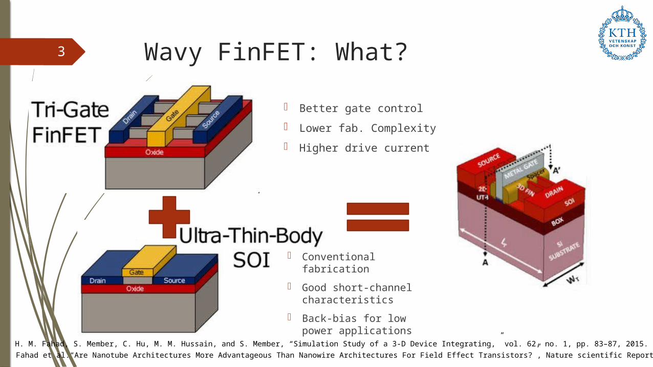
3 Wavy FinFET: What?
Fahad et al.“Are Nanotube Architectures More Advantageous Than Nanowire Architectures For Field Effect Transistors?”, Nature scientific Reports, 2012.
H. M. Fahad, S. Member, C. Hu, M. M. Hussain, and S. Member, “Simulation Study of a 3-D Device Integrating,” vol. 62, no. 1, pp. 83–87, 2015.
Conventional fabrication
Good short-channel characteristics
Back-bias for low power applications
Better gate control
Lower fab. Complexity
Higher drive current

4 Synopsys TCAD Simulation: Parameters
2013 Overall RTC FinFET Parameters:
Top Silicon: 30 nm
BOX: 20nm
Fin width: 6.8 nm
Fin spacing: 19 nm
Fin array termination edge: 25 nm
Fin height: 30 nm
Printed gate length: 18 nm
UTB: 2.5nm, 3.5nm, 4.5 nm
EOT: 0.5 nm (HfO2)
Total device length: 230 nm
Total device width: 108.4 nm
Device area: 0.025 um2
Wavy FinFETSOI Trigate FinFET
H. M. Fahad, S. Member, C. Hu, M. M. Hussain, and S. Member, “Simulation Study of a 3-D Device Integrating,” vol. 62, no. 1, pp. 83–87, 2015.

5 Transfer Characteristics
UTB: 2.5nm, 3.5nm, 4.5 nm
Non-normalized ON-drive: 109% higher
Increase in UTB → ON and OFF currents increase
Lower drive in thinner UTBs
For Trigate with same characteristics:
Larger area
Increased latency
Ultrahigh aspect ration
H. M. Fahad, S. Member, C. Hu, M. M. Hussain, and S. Member, “Simulation Study of a 3-D Device Integrating,” vol. 62, no. 1, pp. 83–87, 2015.
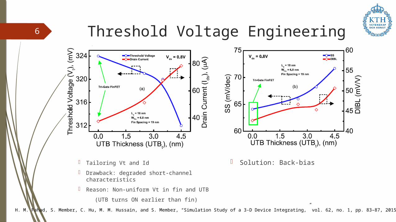
6 Threshold Voltage Engineering
Tailoring Vt and Id
Drawback: degraded short-channel characteristics
Reason: Non-uniform Vt in fin and UTB
(UTB turns ON earlier than fin)
Solution: Back-bias
H. M. Fahad, S. Member, C. Hu, M. M. Hussain, and S. Member, “Simulation Study of a 3-D Device Integrating,” vol. 62, no. 1, pp. 83–87, 2015.

7Reverse and Forward Back Bias
H. M. Fahad, S. Member, C. Hu, M. M. Hussain, and S. Member, “Simulation Study of a 3-D Device Integrating,” vol. 62, no. 1, pp. 83–87, 2015.
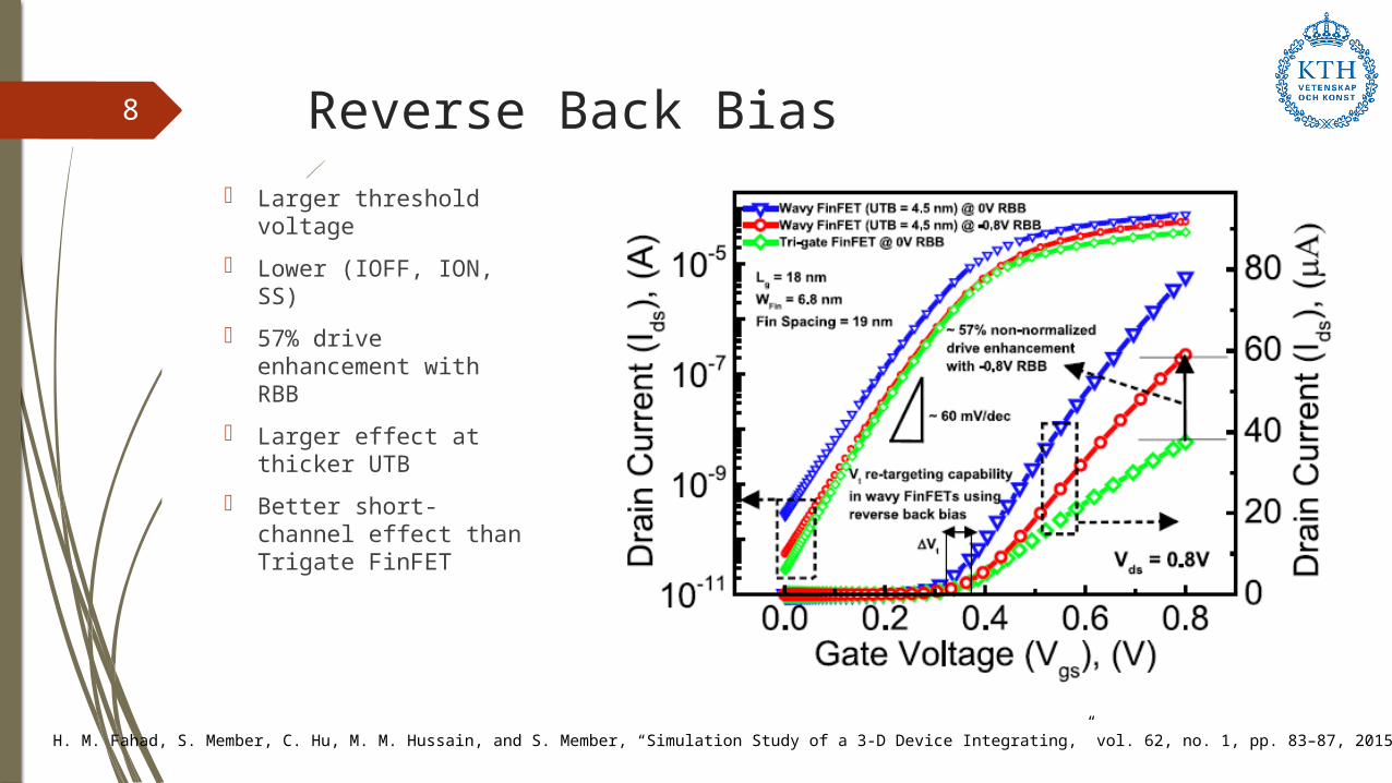
8 Reverse Back Bias
H. M. Fahad, S. Member, C. Hu, M. M. Hussain, and S. Member, “Simulation Study of a 3-D Device Integrating,” vol. 62, no. 1, pp. 83–87, 2015.
Larger threshold voltage
Lower (IOFF, ION, SS)
57% drive enhancement with RBB
Larger effect at thicker UTB
Better short-channel effect than Trigate FinFET

9 Electron Density Distribution
H. M. Fahad, S. Member, C. Hu, M. M. Hussain, and S. Member, “Simulation Study of a 3-D Device Integrating,” vol. 62, no. 1, pp. 83–87, 2015.
𝑉 𝑡 (300𝑚𝑣 )𝑎𝑡𝑉 𝑑𝑠=𝑉 𝑑𝑑 (0.8𝑉 ) 𝑉 𝑔𝑠=𝑉 𝑑𝑠=𝑉 𝑑𝑑(0.8𝑉 )
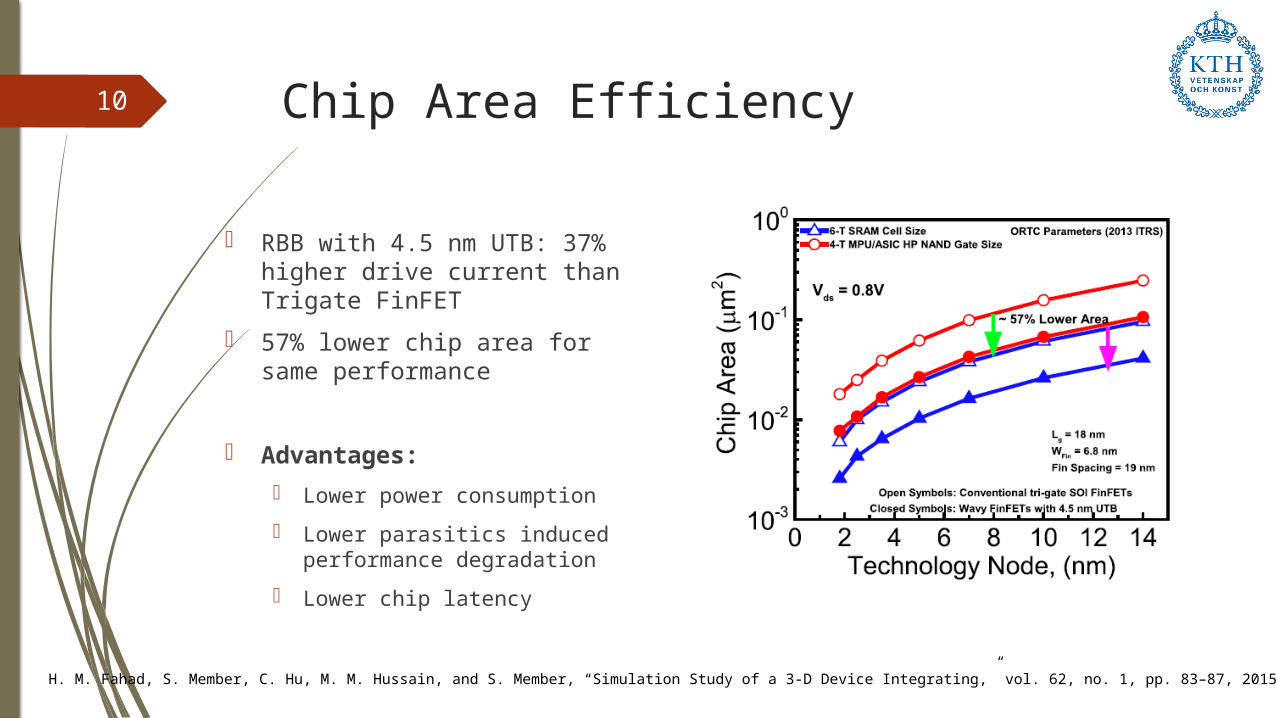
10 Chip Area Efficiency
RBB with 4.5 nm UTB: 37% higher drive current than Trigate FinFET
57% lower chip area for same performance
Advantages:
Lower power consumption
Lower parasitics induced performance degradation
Lower chip latency
H. M. Fahad, S. Member, C. Hu, M. M. Hussain, and S. Member, “Simulation Study of a 3-D Device Integrating,” vol. 62, no. 1, pp. 83–87, 2015.
11 Conclusion
Higher integration density, drive current, are efficiency
Introduces back-biasing for FinFETs
Attractive for high performance computing (servers and supercomputers)
Future:
Fabrication and characterization
UTB process variability effects on performance
UTB and Fin threshold mismatch

12
Related Documents


