W. G. Oldham EECS 42 Spring 2001 Lecture 19 Copyright Regents of University of California cal Limitations of Logic Gates – Week 10a In a computer we’ll have circuits of logic gates to perform specific functions • Computer Datapath: Boolean algebraic functions using binary variables • Symbolic representation of functions using logic gates • Example: D C A B •Every node has capacitance and interconnects have resistance. It takes time to charge these capacitances. •Thus, output of all circuits, including logic gates is delayed from input. •For example we will define the unit gate delay

W. G. Oldham EECS 42 Spring 2001 Lecture 19 Copyright Regents of University of California Physical Limitations of Logic Gates – Week 10a In a computer.
Dec 11, 2015
Welcome message from author
This document is posted to help you gain knowledge. Please leave a comment to let me know what you think about it! Share it to your friends and learn new things together.
Transcript

W. G. OldhamEECS 42 Spring 2001 Lecture 19 Copyright Regents of University of California
Physical Limitations of Logic Gates – Week 10aIn a computer we’ll have circuits of logic gates to perform specific functions
• Computer Datapath: Boolean algebraic functions using binary variables
• Symbolic representation of functions using logic gates• Example:
D
CAB
•Every node has capacitance and interconnects have resistance. It takes time to charge these capacitances.
•Thus, output of all circuits, including logic gates is delayed from input.
•For example we will define the unit gate delay

W. G. OldhamEECS 42 Spring 2001 Lecture 19 Copyright Regents of University of California
UNIT GATE DELAY DTime delay D occurs between input and output: “computation” is not instantaneous Value of input at t = 0+ determines value of output at later time t = D
A
BC
0
1
1
0
Logic State
t
t
D0
0
Input (A and B tied together)
Output

W. G. OldhamEECS 42 Spring 2001 Lecture 19 Copyright Regents of University of California
UNIT GATE DELAY D in ASYNCHRONOUS LOGIC
Time delay D is measured from the last input change
A
BC
0
1
1
0
Logic State
t
t
D0
0
Input B
Output
Input A
W. G. OldhamEECS 42 Spring 2001 Lecture 19 Copyright Regents of University of California
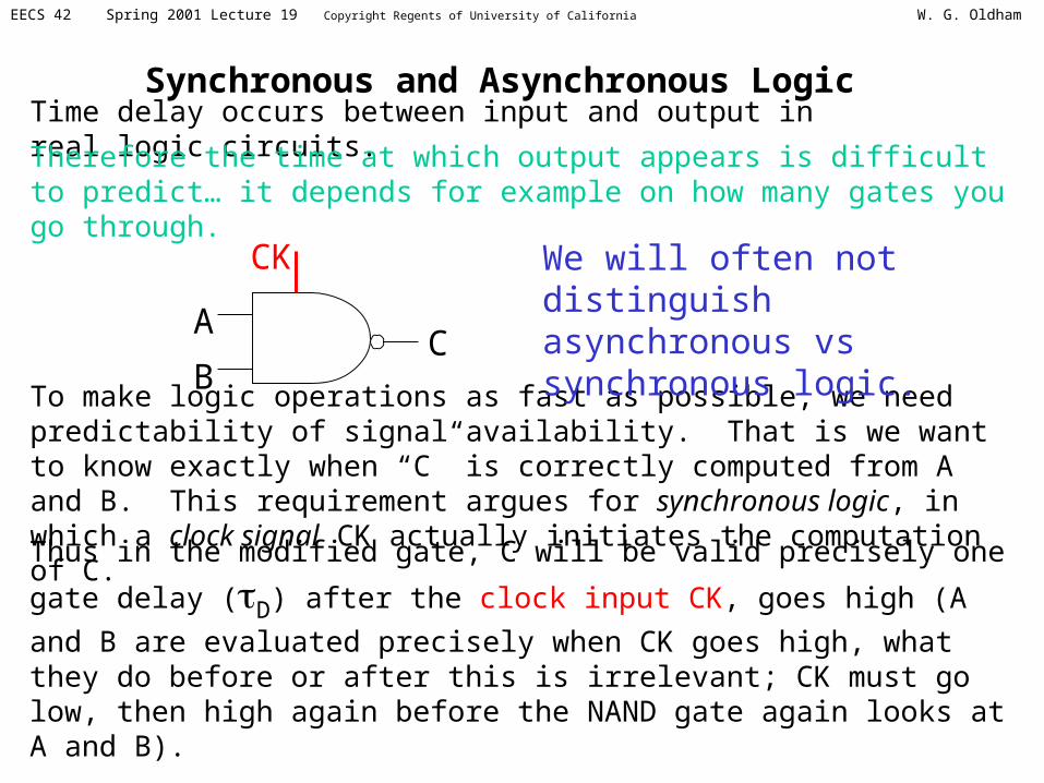
Synchronous and Asynchronous LogicTime delay occurs between input and output in real logic circuits.
Therefore the time at which output appears is difficult to predict… it depends for example on how many gates you go through.
A
BC
Thus in the modified gate, C will be valid precisely one gate delay (D) after
the clock input CK, goes high (A and B are evaluated precisely when CK goes high, what they do before or after this is irrelevant; CK must go low, then high again before the NAND gate again looks at A and B).
CK
To make logic operations as fast as possible, we need predictability of signal availability. That is we want to know exactly when “C” is correctly computed from A and B. This requirement argues for synchronous logic, in which a clock signal CK actually initiates the computation of C.
We will often not distinguish asynchronous vs synchronous logic.

W. G. OldhamEECS 42 Spring 2001 Lecture 19 Copyright Regents of University of California
EFFECT OF GATE DELAY
Cascade of Logic Gates
AB
C
D
Inputs have different delays, but we ascribe a single worst-case delay D to every gate
How many “gate delays for shortest path? ANSWER : 2
How many gate delays for longest path? ANSWER : 3
Which path is the important one? ANSWER : LONGEST

W. G. OldhamEECS 42 Spring 2001 Lecture 19 Copyright Regents of University of California
C,B,A
D
)BA(
)(__
CB
B
D
t
t
t
t
t
Logic state
D
D
D
2D
2D
0
3D
D
TIMING DIAGRAMS
Show transitions of variables vs time
AB
C
Note that becomes valid two gate delays after B&C switch, because the invert function takes one delay and the NAND function a second.
)(__
CB
No change at t = 3 D
Note becomes valid one gate delay after B switches
B
W. G. OldhamEECS 42 Spring 2001 Lecture 19 Copyright Regents of University of California
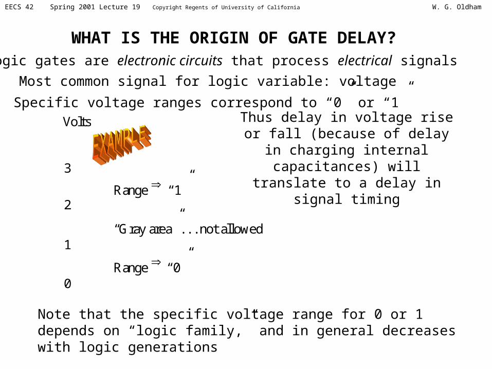
WHAT IS THE ORIGIN OF GATE DELAY?Logic gates are electronic circuits that process electrical signals
Most common signal for logic variable: voltage
Note that the specific voltage range for 0 or 1 depends on “logic family,” and in general decreases with logic generations
Specific voltage ranges correspond to “0” or “1”
Thus delay in voltage rise or fall (because of delay in charging
internal capacitances) will translate to a delay in signal timing
3
2
1
0
Volts
Range “0”
Range “1”
“Gray area” . . . not allowed
W. G. OldhamEECS 42 Spring 2001 Lecture 19 Copyright Regents of University of California
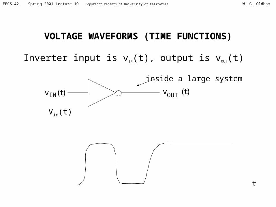
VOLTAGE WAVEFORMS (TIME FUNCTIONS)
Inverter input is vIN(t), output is vOUT(t)
inside a large system
)t(v IN )t(vOUT
t
Vin(t)

W. G. OldhamEECS 42 Spring 2001 Lecture 19 Copyright Regents of University of California
Approximation
D
GATE DELAY (PROPAGATION DELAY)
Define as the delay required for the output voltage to reach 50% of its final value. In this example we will use 3V logic, so halfway point is 1.5V.Inverters are designed so that the gate delay is symmetrical (rise and fall)
Vin(t)
t
1.5
Vout(t)
t
1.5
D D

W. G. OldhamEECS 42 Spring 2001 Lecture 19 Copyright Regents of University of California
EFFECT OF PROPAGATION DELAY ON PROCESSOR SPEED
Computer architects would like each system clock cycle to have between 20 and 50 gate delays … use 35 for calculations
Implication: if clock frequency = 500 MHz clock period = (5108 s1)1
Period = 2 10 9s = 2 ns (nanoseconds)
Gate delay must be D = (1/35) Period = (2 ns)/35 = 57 ps (picoseconds)
How fast is this? Speed of light: c = 3 108 m/s
Distance traveled in 57 ps is:
C X D = (3x10⁸m/s)(57x10-12s) = 17 x 10-4 m = 1.7cm
W. G. OldhamEECS 42 Spring 2001 Lecture 19 Copyright Regents of University of California
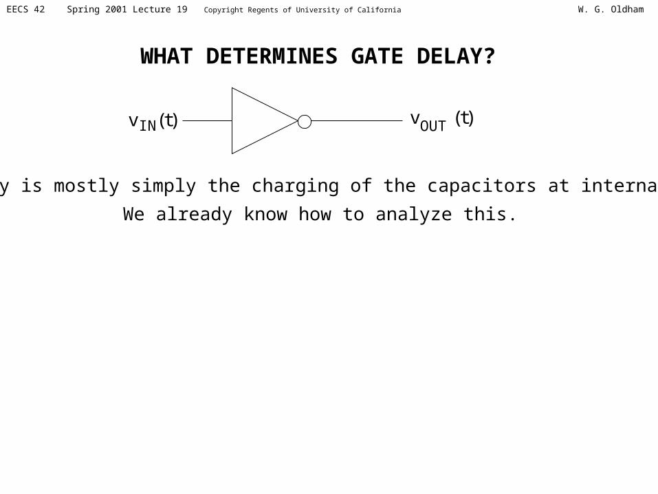
WHAT DETERMINES GATE DELAY?
)t(v IN )t(vOUT
The delay is mostly simply the charging of the capacitors at internal nodes.
We already know how to analyze this.

W. G. OldhamEECS 42 Spring 2001 Lecture 19 Copyright Regents of University of California
ExampleThe gate delay is simply the charging of the capacitors
at internal nodes.Oversimplified example using “ideal inverter, II”
and 5V logic swing
)t(vOUT
)t(v IN2.5
5)t(v IN )t(vOUT
RC = 0.1ns so 0.069ns after vIN switches by 5V, Vx moves 2.5V t
vIN
2.5
5
Vx
D = 0.069ns
vOUT
)t(v IN )t(vOUTIIR
C
Vx
RC = 0.1ns
MODEL
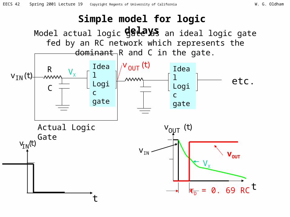
W. G. OldhamEECS 42 Spring 2001 Lecture 19 Copyright Regents of University of California
Simple model for logic delaysModel actual logic gate as an ideal logic gate fed by an
RC network which represents the dominant R and C in the gate.
)t(vIN
t
vIN
VX
D = 0. 69 RC
vOUT
)t(v IN
)t(vOUT
R
C
Ideal Logic gate
Actual Logic Gate
Ideal Logic gate
t
VX
)t(vOUT
etc.

W. G. OldhamEECS 42 Spring 2001 Lecture 19 Copyright Regents of University of California
How can we build inverters, NAND gates, etc. ?
We need some sort of controlled switch: that is a device in which a switch opens or closes in response to an input voltage (a control voltage). If we have a controlled switch it is an easy matter to build inverters, NAND gates, etc.
For example an electromagnetic relay has a coil producing a magnetic field causing some contacts to “snap shut” when a voltage is applied to the coil.
Lets imagine a simple controlled switch, but include in it some resistance (all real devices have non-zero resistance).

W. G. OldhamEECS 42 Spring 2001 Lecture 19 Copyright Regents of University of California
Controlled Switch Model
The basic idea: We need a switch which is controlled by an input voltage. For example: Input V = 0 means the switch is open, whereas an input voltage of 2V means that the switch is closed
(We will call this a “Type N controlled switch”)
VInput
Output
R
+
-
+
-
IInput high
I Output I vs. V
Input low

W. G. OldhamEECS 42 Spring 2001 Lecture 19 Copyright Regents of University of California
Controlled Switch Model
Now lets combine these switches to make an inverter.
-
Type N controlled switch” means switch is closed if input is high. (VG > VS)
Type P controlled switch” means switch is closed if input is low. (VG < VS)
Output
S
Input
RP
-
++
-
+
-G
Input
OutputRN +
+
-
+
-G
S

W. G. OldhamEECS 42 Spring 2001 Lecture 19 Copyright Regents of University of California
Controlled Switch Model of Inverter
So if VIN is 2V then SN is closed and SP is open. Hence VOUT is zero.
Input OutputRN
-
+
SP is closed if VIN < VDD
RP
-
+
+
-
+
-
VDD = 2V
VSS = 0V
SN
SP
SN is closed if VIN > VSS
VIN VOUT
But if VIN is 0V then SP is closed and SN is open. Hence VOUT is 2V.

W. G. OldhamEECS 42 Spring 2001 Lecture 19 Copyright Regents of University of California
Controlled Switch Model of Inverter
IF VIN is 2V then SN is closed and SP is open. Hence VOUT is zero (but driven through resistance RN).
RN
+
--
VDD = 2V
VSS = 0V
VIN =2V
VOUT
But if VIN is 0V then SP is closed and SN is open. Hence VOUT is 2V (but driven through resistance RP).
+
--
VDD = 2V
VSS = 0V
VIN =0V RP
VOUT

W. G. OldhamEECS 42 Spring 2001 Lecture 19 Copyright Regents of University of California
VIN jumps from 0V to 2V
Controlled Switch Model of Inverter
IF there is a capacitance at the output node (there always is) then VOUT responds to a change in VIN with our usual exponential form.
VOUT
t
VIN jumps from 2V to 0V
RN
+
--
VDD = 2V
VSS = 0V
VIN =2V
VOUT
+
--
VDD = 2V
VSS = 0V
VIN =0V RP
VOUT
W. G. OldhamEECS 42 Spring 2001 Lecture 19 Copyright Regents of University of California
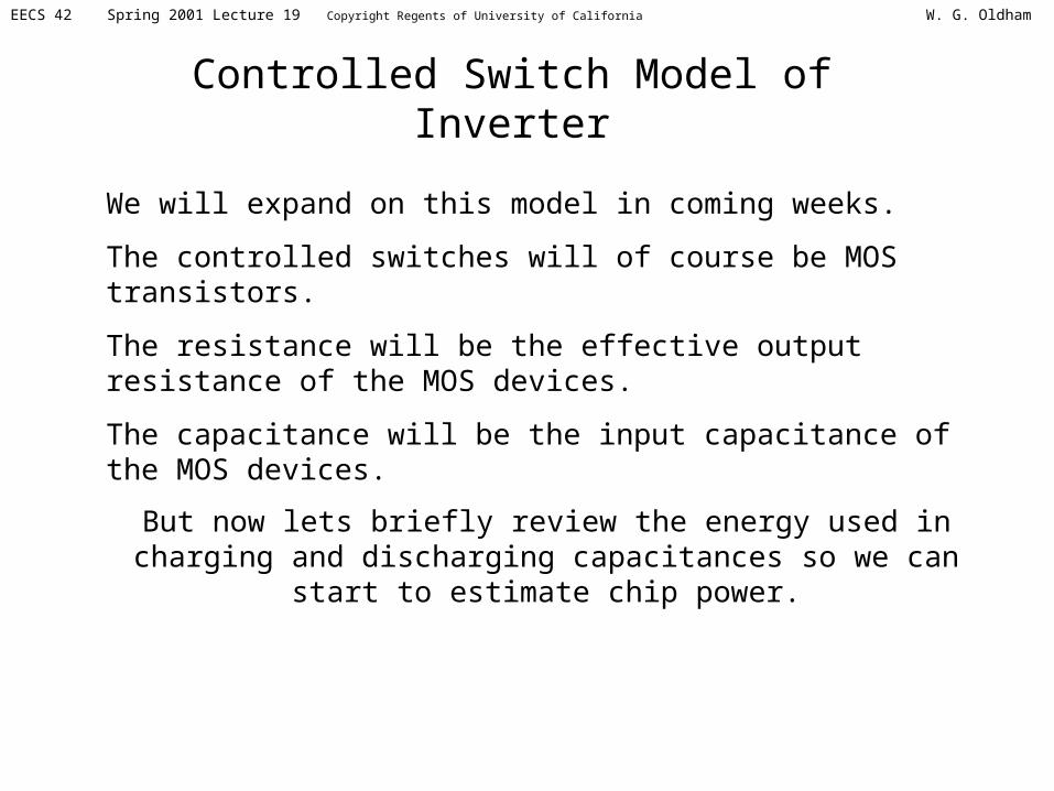
Controlled Switch Model of Inverter
We will expand on this model in coming weeks.
The controlled switches will of course be MOS transistors.
The resistance will be the effective output resistance of the MOS devices.
The capacitance will be the input capacitance of the MOS devices.
But now lets briefly review the energy used in charging and discharging capacitances so we can start to estimate chip power.

W. G. OldhamEECS 42 Spring 2001 Lecture 19 Copyright Regents of University of California
ENERGY AND POWER IN CHARGING/DISCHARGING CAPACITORS – A REVIEW
Capacitor initially uncharged (Q=CVDD at end)
Switch moves @ t=0
Energy out of "battery"
DDV)t(iP
2DD
DD0
DD
CV
QVdtiVE
This must be difference
of E and EC, i.e.
2DDCV
21
CASE 1-Charging
iVDD
t=0R
CRD
R)t(iP 2R
Energy into R (heat)
Power out of "battery" Power into RPower into C
)t(V)t(iP CC
0CC dtiVE
2DDCV
21
Energy into C
W. G. OldhamEECS 42 Spring 2001 Lecture 19 Copyright Regents of University of California
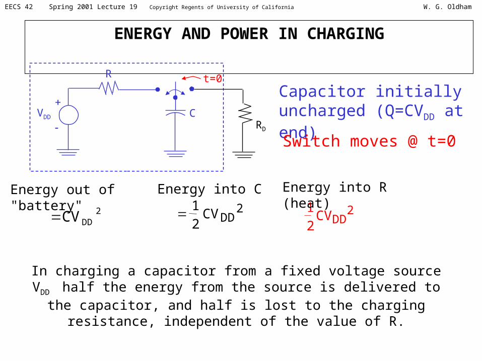
ENERGY AND POWER IN CHARGING
Capacitor initially uncharged (Q=CVDD at end)
Switch moves @ t=0
Energy out of "battery"
2DDCV 2
DDCV21
Energy into R (heat)
2DDCV
21
Energy into C
VDD
t=0R
CRD
In charging a capacitor from a fixed voltage source VDD half the energy from the source is delivered to the capacitor, and
half is lost to the charging resistance, independent of the value of R.
W. G. OldhamEECS 42 Spring 2001 Lecture 19 Copyright Regents of University of California
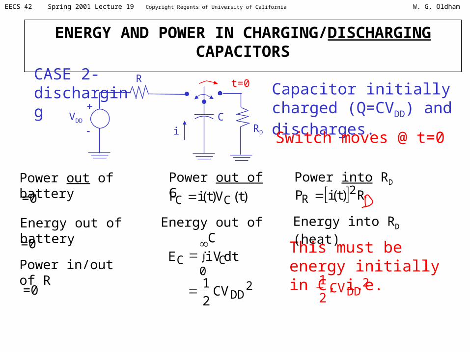
ENERGY AND POWER IN CHARGING/DISCHARGING CAPACITORS
Capacitor initially charged (Q=CVDD) and discharges.
Switch moves @ t=0
Energy out of battery
This must be energy initially in C, i.e.
2DDCV
21
CASE 2-discharging
iVDD
t=0R
CRD
R)t(iP 2R
Energy into RD (heat)
Power out of battery Power into RDPower out of C
)t(V)t(iP CC
0CC dtiVE
2DDCV
21
Energy out of C
=0
=0
Power in/out of R
=0
W. G. OldhamEECS 42 Spring 2001 Lecture 19 Copyright Regents of University of California
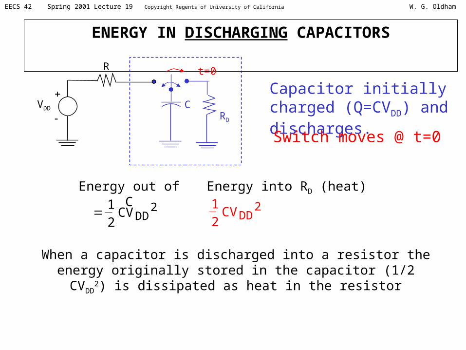
ENERGY IN DISCHARGING CAPACITORS
Capacitor initially charged (Q=CVDD) and discharges.
Switch moves @ t=0
2DDCV
21
VDD
t=0R
CRD
Energy into RD (heat)
2DDCV
21
Energy out of C
When a capacitor is discharged into a resistor the energy originally stored in the capacitor (1/2 CVDD
2) is dissipated as heat in the resistor
W. G. OldhamEECS 42 Spring 2001 Lecture 19 Copyright Regents of University of California
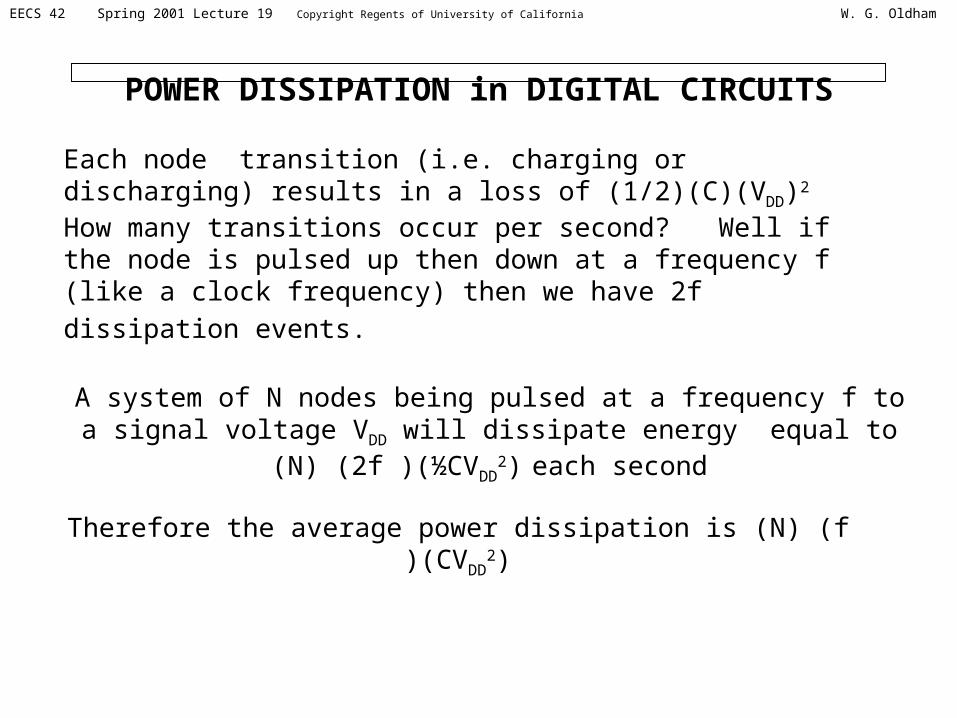
Each node transition (i.e. charging or discharging) results in a loss of (1/2)(C)(VDD)2 How many transitions occur per second? Well if the node is pulsed up then down at a frequency f (like a clock
frequency) then we have 2f dissipation events.
POWER DISSIPATION in DIGITAL CIRCUITS
A system of N nodes being pulsed at a frequency f to a signal voltage VDD will dissipate energy equal to (N) (2f )(½CVDD
2) each second
Therefore the average power dissipation is (N) (f )(CVDD2)

W. G. OldhamEECS 42 Spring 2001 Lecture 19 Copyright Regents of University of California
LOGIC POWER DISSIPATION
Power = (Number of gates) x (Energy per cycle) x (frequency)
N = 107; VDD = 2 V; node capacitance = 10 fF; f = 109 s-1 (1GHz)
P = 400 W! -- a toaster!
Pretty high but realistic
What to do? (N increases, f increases, hmm) 1) Lower VDD
2) Turn off the clock to the inactive nodes
Clever architecture and design!
Lets define as the fraction of nodes that are clocked (active). Then we have a new formula for power.
P = (N) (CVDD2) (f )
W. G. OldhamEECS 42 Spring 2001 Lecture 19 Copyright Regents of University of California
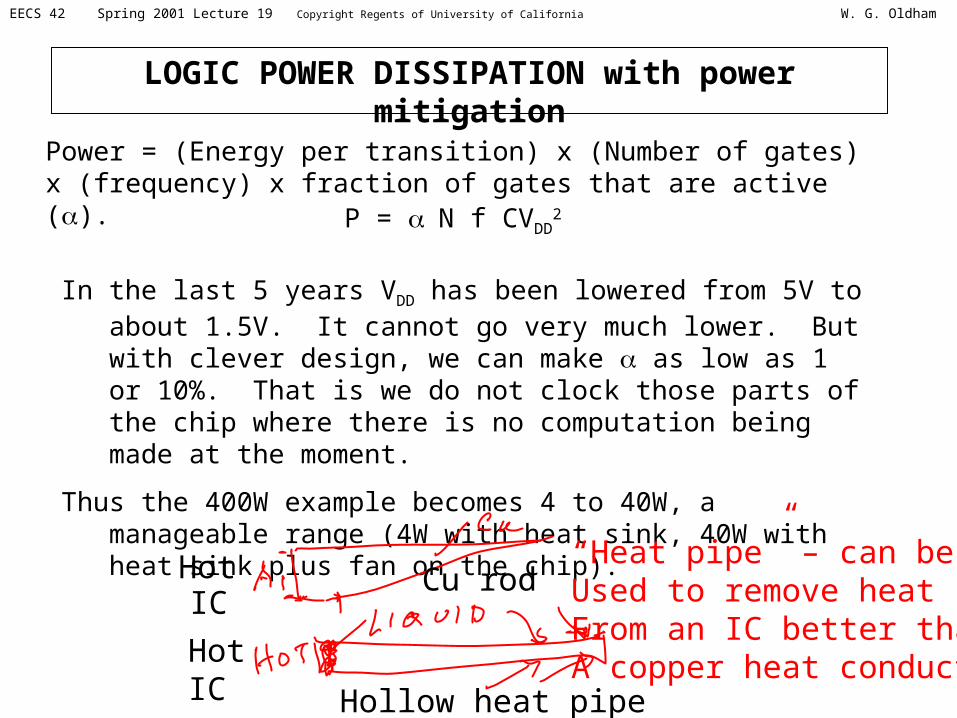
LOGIC POWER DISSIPATION with power mitigation
Power = (Energy per transition) x (Number of gates) x (frequency) x fraction of gates that are active ().
In the last 5 years VDD has been lowered from 5V to about 1.5V. It cannot go very much lower. But with clever design, we can make as low as 1 or 10%. That is we do not clock those parts of the chip where there is no computation being made at the moment.
Thus the 400W example becomes 4 to 40W, a manageable range (4W with heat sink, 40W with heat sink plus fan on the chip).
P = N f CVDD2
“Heat pipe” – can beUsed to remove heatFrom an IC better thanA copper heat conductor
ICHot
HotIC
Cu rod
Hollow heat pipe
Related Documents


