
Welcome message from author
This document is posted to help you gain knowledge. Please leave a comment to let me know what you think about it! Share it to your friends and learn new things together.
Transcript


A RECONFIGURABLE ANALOG-TO-DIGITAL CONVERTER FOR A MOBILE RECEIVER
Aleksandar Stojcevski, B.EngEE, M.EngEE
SUBMITTED IN FULFILLMENT OF THE REQUIREMENTS FOR THE DEGREE OF DOCTOR OF PHILOSOPHY
VICTORIA ^ UNIVERSITY
School of Electrical Engineering
Faculty of Science, Engineering and Technology
Victoria University
PC Box 14428
Melbourne City MC
Victoria, Australia, 8001

FTS THESIS 621.38456 STO 30001007971825 Stojcevski, Aleksandar A reconfigurable analog-to-digital converter for a mobile receiver

My work is dedicated to the two most important people in my life to date.
My wife Klementina Stojcevski, whose encouragement, support and endless love has made me the man I am today.
The other is my new born son Stefan Stojcevski, whose entrance on the l4 of May 2003, in this huge world has given me another reason to live.
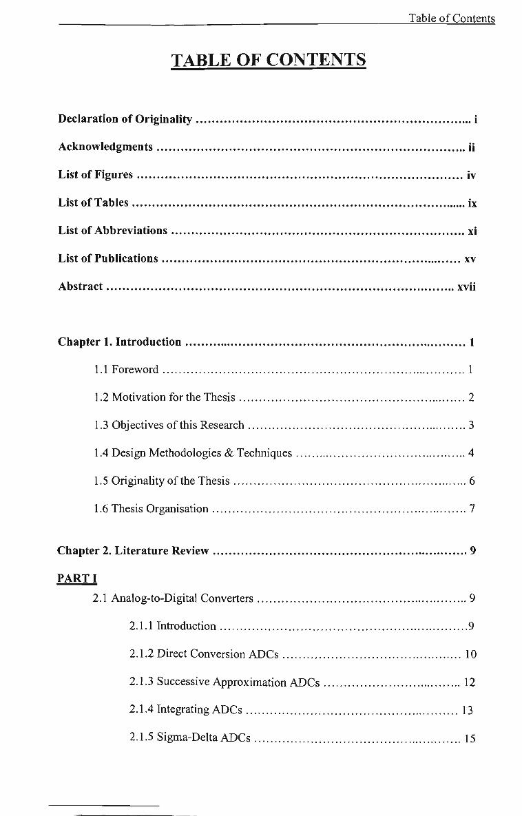
Table of Contents
TABLE OF CONTENTS
Declaration of Originality i
Acknowledgments ii
List of Figures iv
List of Tables ix
List of Abbreviations xi
List of Publications xv
Abstract xvii
Chapter 1. Introduction 1
1.1 Foreword 1
1.2 Motivation for the Thesis 2
1.3 Objectives of this Research 3
1.4 Design Methodologies & Techniques 4
1.5 Originality of the Thesis 6
1.6 Thesis Organisation 7
Chapter 2. Literature Review 9
PARTI
2,1 Analog-to-Digital Converters 9
2.1.1 Introduction 9
2.1.2 Direct Conversion ADCs 10
2.1.3 Successive Approximation ADCs 12
2.1.4 Integrating ADCs 13
2.1.5 Sigma-Delta ADCs 15
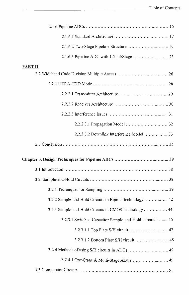
Table of Contents
2.1.6 Pipeline ADCs 16
2.1.6.1 Standard Architecture 17
2.1.6.2 Two-Stage Pipeline Structure 19
2.1.6.3 Pipeline ADC with 1.5-bit/Stage 23
PART II
2.2 Wideband Code Division Multiple Access 26
2.2.1 UTRA-TDD Mode 28
2.2.2.1 Transmitter Architecture 29
2.2.2.2 Receiver Architecture 30
2.2.2.3 Interference Issues 31
2.2.2.3.1 Propagation Model 32
2.2.2.3.2 Downlink Interference Model 33
2.3 Conclusion 35
Chapter 3. Design Techniques for Pipeline ADCs 38
3.1 Introduction 38
3.2. Sample-and-Hold Circuits 38
3.2.1 Techniques for Sampling 39
3.2.2 Sample-and-Hold Circuits in Bipolar technology 42
3.2.3 Sample-and-Hold Circuits in CMOS technology 44
3.2.3.1 Switched Capacitor Sample-and-Hold Circuits 46
3.2.3.1.1 Top Plate S/H circuit 47
3.2.3.1.2 Bottom Plate S/H circuit 48
3.2.4 Methods of using S/H circuits in ADCs 49
3.2.4.1 One-Stage & Multi-stage ADCs 49
3.3 Comparator Circuits 51

Table of Contents
3.3.1 Offset Cancellation Techniques 51
3.3.1.1 Circuit Topologies 51
3.3.1.2 Design Constraints in a CMOS Latch 54
3.4 Operational Amplifier Circuits 56
3.4.1 Telescopic Cascode Amplifier Design 56
3.4.2 Folded Amplifier Design 58
3.4.3 Miller AmpHfier Design 60
3.5 Digital-to-Analog Converter Architectures 61
3.5.1 Charge Division Architecture 61
3.5.2 Current Division Architecture 63
3.5.3 Resistor-Ladder Architecture 64
3.6 Proposed Circuit Techniques for most Critical components in ADC 65
3.6.1 Proposed Sample-and-Hold Circuit 65
3.6.2 Proposed Comparator Circuit 68
3.6.2.1 Comparator Optimisation 71
3.6.2.1.1 PMOS Differential Pair Optimisation 72
3.6.2.1.2 NMOS Regeneration Circuit Optimisation...73
3.6.2.1.3 S-R Latch Optimisation 75
3.6.2.2 Comparator Analysis 76
3.7 Conclusion 77
Chapter 4. Sub-ADC Architecture 79
4.1 Introduction 79
4.2 ADC Specifications 80
4.2.1 Static Specifications 80

Table of Contents
4.2.1.1 ADC Differential Non-Linearity (DNL) 80
4.2.1.2 ADC Integral Non-Linearity (INL) 81
4.2.2 Distortion Characteristics (Dynamic Specifications) 82
4.2.2.1 Total Harmonic Distortion 83
4.2.2.2 Signal-to-Noise Ratio 83
4.2.2.3 Signal-to-Noise plus Distortion Ratio 84
4.2.2.4 Effective Number of Bits 85
4.2.2.5 Spurious Free Dynamic Range 86
4.2.3 Receiver ADC Dynamic Range Analysis 86
4.3 First Pipeline ADC Stage 88
4.3.1 Sub-ADC (Modified-Flash) Architecture 88
4.3.1.1 Noise Analysis 92
4.3.1.1.1 Resistor Ladder Noise Analysis 92
4.3.1.1.2 2:1-Switch Noise Analysis 93
4.3.1.1.3 4:1-Switch Noise Analysis 96
4.3.1.1.4 Comparator Noise Analysis 97
4.3.1.2 Probability Analysis 99
4.3.2 Analysis ofthe Modified-Flash ADC 102
4.4 Conclusion 105
Chapters. Reconfigurable ADC with Fixed Filter 106
5.1 Introduction 106
5.2 Reconfigurable Pipeline ADC Design 108
5.2.1 Algorithm Formulation 108
5.2.2 Receiver Architecture with Reconfigurable ADC 112
5.2,2,1 Pipeline ADC Structure 113

Table of Contents
5.2.2.2 Decimation Factor 114
5.2.2.3 Signal Power Measurement 115
5.2.2.3.1 Full Wave Rectifier 115
5.2.2.3.2 Averaging Filter 116
5.2.2.4 Control Unit 118
5.3 Statistical Analysis 121
5.3.1 Simulation Enviroimient 121
5.3.2 Statistical Results 122
5.4 Implementation ofthe Reconfigurable ADC 126
5.4.1 Design Flow and Techniques 126
5.4.1.1 CMOS IC Design Flow 126
5.4.1.2 ADC Digital Section 129
5.4.1,2.1 Domino Logic 129
5.4.2 Layout Considerations 130
5,4,2,1 Mixed-Signal Layout Considerations 131
5.4.2.1.1 Floor-Planning 132
5.4.2.1.2 Power Supply and Ground Considerafions,133
5.4.2.1.3 Guard Rings 134
5.4.2.1.4 Shielding 135
5.4.3 Reconfigurable ADC Layout 135
5.5 Conclusion 139
Chapter 6. Effect of Scalable Filter on the Reconfigurable ADC
Architecture 141
6.1 Introduction 141
6.2 System Design 143

Table of Contents
6.2.1 Filter Considerations 143
6.2.2 Scalable RRC Filter 146
6.2.3 Modified Control Unit 149
6.3 Statistical Analysis 155
6.4 Conclusion 160
Chapter 7. Conclusions & Future Work 162
7.1 Introduction 162
7.2 Maj or Findings 163
7.3 Assumptions 167
7.4 Future Work 168
Bibliography 171
Appendix A. Spreading & Modulation in TDD 180
Appendix B. Comparator Noise Analysis 194
Appendix C. Cadence Power Consumption Measurement Flow 202

Declaration of Originality
Declaration of Originality
I declare that, to the best of my knowledge, the research described herein is the result of
my own work, except where otherwise stated in the text. It is submitted in fiilfillment of
the candidature for the degree of Doctor of Philosophy in Engineering at Victoria
University, Melbourne, Australia, No part of this work has been submitted for any other
degree.
A AJIXS^^^
Aleksandar Stojcevski

Acknowledgments
Acknowledgements
First I would like to express my sincere appreciation to my supervisors Professor
Jugdutt (Jack) Singh and Associate Professor Aladin Zayegh. Numerous motivating
and instructive discussions with them are the reason for the success of this project. Their
keen insight into microelectronics and IC design led me into the right direction of the
research, I am gratefiil to their patient guidance and encouragement throughout the
program,
I would also like to thank Professor Mike Faulkner for all the discussions and help on
the telecommunication section of my research, I would like to thank my colleagues
within the Telecommunications & Microelectronics group. In particular, I thank Rormy
Veljanovski for many long hours with me discussing various issues about the UTRA-
TDD system.
My gratitude also goes to Professor Akhtar Kalam, for his valuable suggestions and
discussions related to research, I'm also very gratefiil to the administration staff at
Victoria University, particularly Shirley Herrewyn and Maria Pylnyk, I would also like
n

Acknowledgments
to thank my colleagues and my fellow Chipskills assistants, Phuoc Nguyen, Vidya
Vibhute, Hai Le, Lei Huang, Cagil Ozansoy, Leon Gor and others for making my life at
Victoria University colorfiil.
My gratitude also goes to Dr, Song Cui from Semiconductor Technologies Australia,
the Australian Telecommunications Cooperative Research Centre (ARCRC) and the
Australia Federal Government for their financial support throughout my PhD program.
Large thanks must also go to my father Mr. Rade Stojcevski, and my parents-in-law,
Mr, Stance Gikovski and Mrs, Vesa Gikovska for their support, A special thanks goes
out to my brother-in-law, Valentino Gikovski for his words of encouragement.
Last, but not least, I would like to thank my wife Klementina Stojcevski and my son
Stefan Stojcevski, Their faith in me and never ceasing love are the impetus of my hard
work.
ni

List of Figures
List of Figures
Figure 1,1: Direct conversion receiver architecture 2
Figure 1.2: Mobile Terminal Receiver with Reconfigurable Properties 7
Figure 2,1: ADCs based on the direct-conversion architecture 11
Figure 2,2: Typical successive approximation ADC 12
Figure 2,3: Dual-Slope Integrating ADC 13
Figure 2,4: Timing relationships for a dual-slope integrating ADC 14
Figure 2,5: Sigma-delta converter 15
Figure 2,6: Standard Pipeline ADC block diagram 17
Figure 2,7: Single Pipeline stage block diagram 18
Figure 2,8: -bit ADC 19
Figure 2.9: Two-stage Pipeline ADC 20
Figure 2.10: Digital correction for (5+^- l)-bitADC 21
Figure 2.11: Single stage, 1,5-bit/stage pipeline ADC 23
Figure 2.12: Sub-DAC outputs, 1,5-bit/stage pipeline ADC 24
Figure 2,13: Digital error correction for 1,5-bit/stage pipeline ADC 25
Figure 2,14: UTRA duplex modes 26
Figure 2,15: UTRA-TDD Base band Transmitter (one time slot) 29
iv

List of Figures
Figure 2,16: UTRA-TDD Receiver architecture for one time slot 30
Figure 3,1: Parallel Sampling 38
Figure 3,2: Series Sampling 38
Figure 3,3: A typical CMOS switch 40
Figure 3,4: Input dependent sampling stage 40
Figure 3,5: Distortion due to disparity of switch on-resistance 40
Figure 3.6: Simplified diode bridge 41
Figure 3.7: Bridge with top diodes removed 42
Figure 3,8: Bridge with input follower 42
Figure 3,9: Unity gain sampling 43
Figure 3,10: Series sampling technique 43
Figure 3,11: S/H circuit architecture with multi-plexed input 44
Figure 3,12: Recycling S/H circuit architecture 45
Figure 3,13: MOS Sample-and-Hold 46
Figure 3,14: Bottom plate sample-and-hold circuit 47
Figure 3.15: Non-linearity of input capacitance in Flash ADC 48
Figure 3,16: Feedback of input signal to resistance ladder 49
Figure 3,17: Bubbles (sparks) appearing from timing disparity 49
Figure 3,18: Comparator offset cancellation techniques (input offset storage) 51
Figure 3,19: Comparator offset cancellation techniques (output offset storage) 51
Figure 3.20: Multi-stage offset cancellation 52
Figure 3.21: Dynamic CMOS latch 53
Figure 3,22: Telescopic Amplifier Circuit 56
Figure 3,23: Folded cascode amplifier 58
Figure 3,24: Two-Stage Miller Amplifier 59
List of Figures
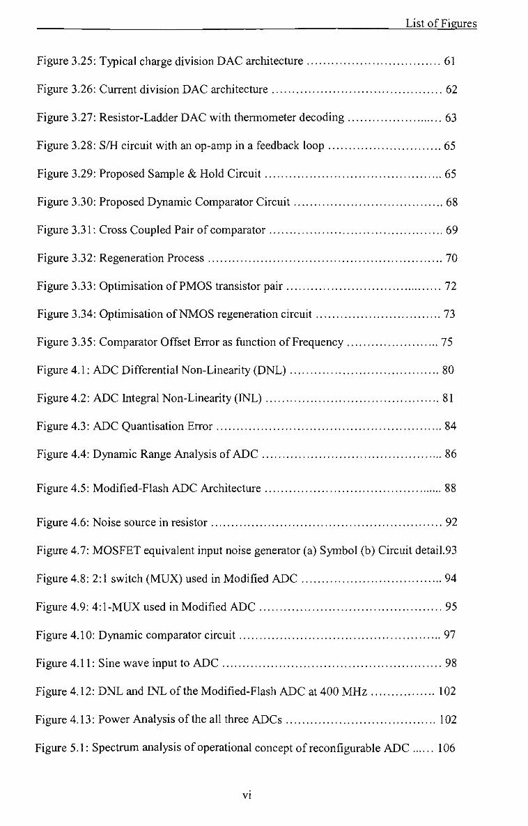
Figure 3,25: Typical charge division DAC architecture 61
Figure 3,26: Current division DAC architecture 62
Figure 3,27: Resistor-Ladder DAC with thermometer decoding 63
Figure 3,28: S/H circuit with an op-amp in a feedback loop 65
Figure 3,29: Proposed Sample & Hold Circuit 65
Figure 3,30: Proposed Dynamic Comparator Circuit 68
Figure 3,31: Cross Coupled Pair of comparator 69
Figure 3,32: Regeneration Process 70
Figure 3,33: Optimisation of PMOS transistor pair 72
Figure 3.34: Optimisation of NMOS regeneration circuit 73
Figure 3.35: Comparator Offset Error as fiinction of Frequency 75
Figure 4,1: ADC Differential Non-Linearity (DNL) 80
Figure 4,2: ADC Integral Non-Linearity (INL) 81
Figure 4,3: ADC Quantisation Error 84
Figure 4.4: Dynamic Range Analysis of ADC 86
Figure 4,5: Modified-Flash ADC Architecture 88
Figure 4,6: Noise source in resistor 92
Figure 4.7: MOSFET equivalent input noise generator (a) Symbol (b) Circuit detail,93
Figure4,8:2:l switch (MUX) used in Modified ADC 94
Figure 4.9: 4:1-MUX used in Modified ADC 95
Figure 4,10: Dynamic comparator circuit 97
Figure 4.11: Sine wave input to ADC 98
Figure 4,12: DNL and INL ofthe Modified-Flash ADC at 400 MHz 102
Figure 4,13: Power Analysis ofthe all three ADCs 102
Figure 5,1: Spectrum analysis of operational concept of reconfigurable ADC 106
VI

List of Figures
Figure 5,2: Downlink ACI scenario in UTRA-TDD 107
Figure 5,3: UTRA-TDD Interference Overlaps 108
Figure 5,4: UTRA-TDD Receiver architecture for one time slot 109
Figure 5.5: Reconfigurable receiver ADC architectural block diagram I l l
Figure 5,6: Reconfigurable Pipeline ADC block diagram 112
Figure 5.7: Decimation operation, down sampling by factor of 4 113
Figure 5,8: Signal Power Measurement 114
Figure 5,9: Two's compliment operation in digital hardware with a word 115
Figure 5,10: Operation ofthe FWR 115
Figure 5,11: RC Low Pass Filter Network 116
Figure 5.12: Digital Low-Pass Filter Network 117
Figure 5,13: Cell topology where muUiple cells are causing ACI 120
Figure 5,14: CDF ofADC word lengths 122
Figure 5.15: CDF ofADC Power Consumption 124
Figure 5,16: CMOS IC design flow 126
Figure 5,17: Design flow employed for reconfigurable ADC 127
Figure 5,18: Domino structure of encoder used 128
Figure 5,19: Mixed-Signal layout strategy 130
Figure 5.20: Mixed-Signal Floor-Plan 131
Figure 5,21: Power and ground connection 132
Figure 5,22: Block Diagram of ADC ASIC 135
Figure 5,23: Layout ofADC ASIC 136
Figure 5,24: Dynamic Power Consumption of ASIC components in ADC at 15,36
MHz 137
Figure 6,1: UTRA-TDD Mobile Receiver with reconfigurable ADC and Filter ,,., 142
vii

List of Figures
Figure 6,2: Transversal FIR filter structure 143
Figure 6,3: Linear Phase FIR filter structure 144
Figure 6,4: Scalable Digital Filter System 146
Figure 6,5: Scalable Digital Filter System (Detailed) 147
Figure 6.6: Reconfigurable Digital Filter Architecture 147
Figure 6,7: Frequency Response using various filter lengths 151
Figure 6,8: Inter-Symbol Interference Analysis 153
Figure 6.9: Combined Reconfigurable Architecture (CRA) 154
Figure 6,10: Statistical analysis of CRA(GA = 0.001 ^ 2 ) 156
Figure 6.11: Statistical analysis of CRA (G t = 4 ^ 10) 156
Figure 6.12: Statistical analysis of CRA (G*-2) 158
Figure 7,1: Schematic representation of a MIMO wireless system 168
Vlll

List of Tables
List of Tables
Table 2,1: Parameters comparison of UTRA-TDD and FDD 27
Table 3,1: Proposed Sample-and-Hold Results 66
Table 3,2: W/L Ratios ofthe PMOS transistors 72
Table 3,3: W/L Ratios of Regeneration circuit transistors 74
Table 3,4: W/L Ratios of S-R Latch 75
Table 3,5: Comparator Results at 2.5V supply 76
Table 4,1: Relationship between comparator outputs and ADC outputs 89
Table 4.2: Probability of each comparator 100
Table 4,3: Summary of noise power in New ADC 100
Table 4,4: Comparison results ofthe ADC circuits at 400 MHz 101
Table 4,5: Number of Comparators required for each Flash design 103
Table 4,6: Comparison results ofthe ADC circuits at 15.36 Ms/s 103
Table 5.1: Confrol Unit Lookup Table 119
Table 5,2: Simulation Parameters
121
Table 5,3: Effect on Resolution with different a 123
Table 5,4: ADC Performance Results 136
IX

List of Tables
Table 5,5: Power Consumption of Reconfigurable ADC 138
Table 6,1: Control Unit Look-up Table for Filter 151
Table 6,2: Base Band Transceiver Parameters 152
Table 6,3: Simulation Parameters 155
Table 6.4: Statistical analysis results of CRA 157

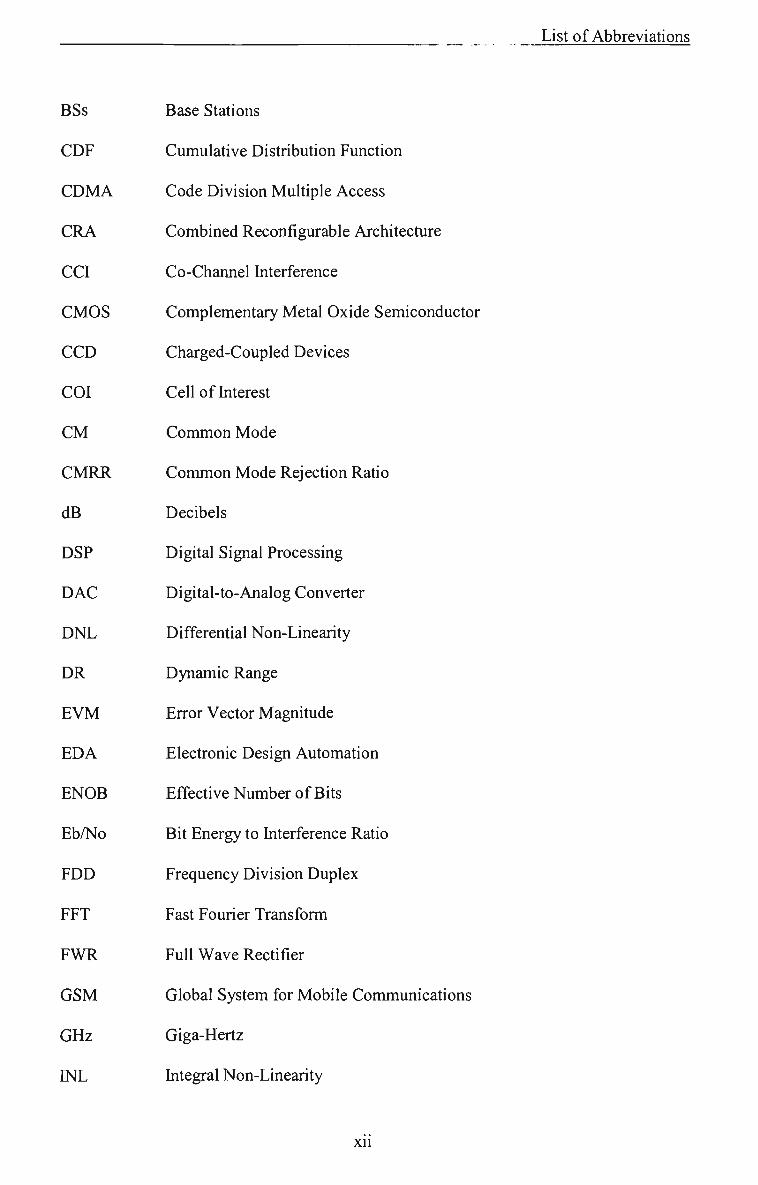
List of Abbreviations
List of Abbreviations
IGS First Generation System
2GS Second Generation System
3G Third Generation
3GS Third Generation System
3GPP Third Generation Partnership Project
w
nV
iV
S-A
ACI
ADC
ACP
ASIC
ACER
AF
ACS
BiCMOS
BS
femto-Fared
Nano-Volts
Micro-Volt
Sigma - Delta
Adjacent Channel Interference
Analog-to-Digital Converter
Adjacent Channel Protection
Application Specific Integrated Circuit
Adjacent Channel Leakage Ratio
Averaging Filter
Adjacent Channel Selectivity
Bipolar Complementary Metal Oxide Semiconductor
Base Station
XI
List of Abbreviations
BSs Base Stations
CDF Cumulative Distribution Function
CDMA Code Division Multiple Access
CRA Combined Reconfigurable Architecture
CCI Co-Channel Interference
CMOS Complementary Metal Oxide Semiconductor
CCD Charged-Coupled Devices
COI Cellofhiterest
CM Common Mode
CMRR Common Mode Rejection Ratio
dB Decibels
DSP Digital Signal Processing
DAC Digital-to-Analog Converter
DNL Differential Non-Linearity
DR Dynamic Range
EVM Error Vector Magnitude
EDA Electronic Design Automation
ENOB Effective Number of Bits
Eb/No Bit Energy to Interference Ratio
FDD Frequency Division Duplex
FFT Fast Fourier Transform
FWR Full Wave Rectifier
GSM Global System for Mobile Communications
GHz Giga-Hertz
INL Integral Non-Linearity
xn
List of Abbreviations
ISI Inter Symbol Interference
ICs Integrated Circuits
lOS Input Offset Storage
LSB Least Significant Bit
LNA Low Noise Amplifier
LPF Low Pass Filter
LUT Look Up Table
MSB Most Significant Bit
MS Mobile Station
MSs Mobile Stations
MSPS Mega-Sample per Second
MHz Mega-Hertz
MAC Multiply-Accumulate
MIMO Multiple hiput Multiple Output
NMOS Negative-Channel Metal Oxide Semiconductor
Nf Nyquist Frequency
OOS Output Offset Storage
OSVF Orthogonal Variable Spreading Factor
PCS Personal Communications System
PDC Personal Digital Communications
PSRR Power Supply Rejection Ratio
PMOS Positive-Channel Metal Oxide Semiconductor
Qn Quantisation Noise
QPSK Quadrature Phase Shift Key
RRC Root Raised Cosine
Xlll

List of Abbreviations
RF
rms
SNDR
SNR
SAR
S/H
SFDR
SDD
SoC
TDD
THD
Radio Frequency
Root Mean Square
Signal-to-Noise plus Distortion Ratio
Signal-to-Noise Ratio
Successive-Approximation Register
Sample-and-Hold
Spurious Free Dynamic Range
Space Division Duplex
System on a Chip
Time Division Duplex
Total Harmonic Distortion
TDMA Time Division Multiple Access
UMTS Universal Mobile Telecommunication System
UTRA UMTS Terrestrial Radio Access
VLSI Very Large Scale Integration
WCDMA Wideband Code Division Multiple Access
xiv

List of PubUcations
List of Publications
Journal Publications
[1] A. Stojcevski, H. P, Le, J. Singh, A. Zayegh, "Flash ADC Architectiire", lEE Journal, Electronic Letters, Vol. 39, No. 6, pp. 501-502, 2003.
[2] A, Stojcevski, R, Veljanovski, J, Singh, M. Faulkner, A. Zayegh, "A Low Cost Reconfigurable Architecture for UMTS Receiver" Accepted for publication in lEICE Transactions on Communications, Special Issue, 2003.
[3] A. Stojcevski, J. Singh, A, Zayegh, "An Efficient ADC for an UTRA-TDD System", Accepted for publication in Advances in Modeling & Simulation, AMSE Journal, 2003.
[4] A, Stojcevski, J, Singh, A, Zayegh, "Low Power, High Speed, 4-Stage Pipehne Analog-to-Digital Converter", Accepted for publication in Advances in Modeling & Simulation, AMSE Best-of-Book Journal, 2002,
[5] A, Stojcevski, R, Veljanovski, J. Singh, A. Zayegh, M. Faulkner, "Reconfigurable Architecture for UTRA-TDD System", lEE Journal, Electronic Letters, Vol. 38, No. 25, pp. 1732-1733, 2002.
[6] A, Stojcevski, J. Singh, A, Zayegh, "Design Implication of the Building Block Components of Pipeline Analog-to-Digital Converters", Accepted for publication in Advances in Modeling & Simulation, AMSE Journal, 2002,
XV

List of Publications
Conference Publications
[1] A, Stojcevski, R, Veljanovski, J, Singh, A, Zayegh, "Highly Efficient Reconfigurable Architecture of UTRA-TDD Mobile Terminal Receiver", Proceeding of IEEE, International Symposium on Circuits and Systems, ISCAS'03, Bangkok, Thailand, pp. n-45 - n-48, 2003
[2] A, Stojcevski, R, Veljanovski, J. Singh, A. Zayegh, "A Real-Time Reconfigurable Pipelined Architecture with Advanced Power management for UTRA-FDD", Proceeding of IEEE, PIMRC, 2003.
[3] A, Stojcevski, H. P. Le, J. Singh, A. Zayegh, "Low Cost Flash Architecture for Pipeline ADC", Proceeding of IEEE, 10* International Conference on Mixed Design of Integrated Circuits and Systems, MIXDES, Poland, 2003,
[4] A. Stojcevski, J. Singh, A, Zayegh, "Scalable Pipeline Analog-to-Digital Converter for UTRA-TDD Mobile Station Receiver", Proceeding of IEEE, International Conference on Semiconductor Electronics", ICSE'02, Penang, Malaysia, pp, 370-374, 2002.
[5] A. Stojcevski, J, Singh, A, Zayegh, "Modified Flash ADC Architecture with Reduced Power and Complexity", Proceedings of the 4' International Conference on Modeling and Simulation, MS'02, Melbourne, Australia, pp, 169-173,2002,
[6] A, Stojcevski, J. Singh, A, Zayegh, "A Reconfigurable Analog-to-Digital Converter for UTRA-TDD Mobile Terminal Receiver", Proceeding of IEEE, Midwest Symposium on Circuits and Systems, MWSCAS, Tulsa, Oklahoma, USA, pp, n-613 - n616, 2002.
[7] A. Stojcevski, J, Singh, A. Zayegh, "Quantisation Error Analysis for an ADC used in UTRA-TDD Mobile Station Receiver", Proceedings ofthe 2"'' ATCRC Telecommunications and Networking Conference, Fremantle, Ausfralia, pp, 2002. (Best Paper Award).
[8] A, Stojcevski, J, Singh, A, Zayegh, "Performance Analysis of a CMOS Analog to Digital Converter for Wireless Telecommunications," Proceedings of IEEE, ISIC-2001, Devices & Systems, Marina Mandarin, Singapore, pp, 59-62,2001.
XVI
Absfract
Abstract
The evolution of new telecommunication standards is increasingly leaning towards
higher data transmission rates. The boundaries between digital and analog signal
processing is impending closer to the antenna, therefore aiming for a software-defined
radio solution. In terms of analog-to-digital converters (ADCs) of mobile terminal
receivers, this indicates higher sample rate, lower power consumption and higher
resolution. With comparison to other ADCs, the pipelined ADC architecture has most
successfiilly covered the wide resolution limits and data rate requirements of these
terminal receiver architectures. However, even though fix word-length pipeline ADC
architecture could be a suitable device for the mobile receiver, it still has a distinct
disadvantage when it comes to power consumption. ADC optimisation techniques could
lower power consumption but will not reduce it to its most efficient level,
A solution in theory is to use minimum resolution, and still meet the performance
requirements of the Universal Mobile Telephone Service (UMTS) Terrestrial Radio
Access (UTRA) - Time Division Duplex (TDD) receiver specified by the 3' '
xvu

_ ^ Absfract
Generation Partnership Project (3GPP). To achieve this, in-band and out-of-band signal
powers need to be measured. The ADC then intelligently chooses the amount of
resolution required to ensure the out-of-band signal is below a certain tolerance level
and the Signal-to-Noise Ratio (SNR) is met. This scheme will reduce power
consumption, as it only utilises the required resolution as compared to traditional fixed
complexity architectures. To solve this, a more complex receiver ADC design and
implementation is required, which will have a significant impact on battery life in the
mobile terminal. Taking advantage of the software-defined radio theory, a solution can
be achieved using digital signal processing and application specific integrated circuit
(ASIC) technologies that can meet the performance and system needs of high speed and
low cost devices, A DSP can interface with an ASIC and control the ADC resolution
dependant on in-band and out-of-band power ratios, making the design a reconfigurable
solution. This could be embedded on a single chip to provide System-on-a-Chip (SoC)
solution.
In this thesis, the requirements of ADC of the mobile receiver architecture are studied
and analysed using the system specifications ofthe 3' '' Generation (3G) Wideband Code
Division Multiple Access (WCDMA) standard. From the standard and limited
performance of the building blocks, constraints at circuit design level and block level,
within the design ofthe pipeline ADCs are drawn. At the circuit level, topologies for the
most important components of the pipeline ADC have been developed and analysed.
These include a sample-and-hold (S/H) circuit and a dynamic comparator.
xvni

Absfract
The emphasis of the thesis is based on the reconfigurable properties of the pipeline
ADC, to be used within the mobile receiver, A reconfigurable 4-bit to 16-bit, 15.36-
MS/s embedded CMOS pipeline ADC, optimised for low-power direct conversion
receiver has been designed. The research was fiirther extended by making the Root
Raised Cosine (RRC) filter, also part of the mobile receiver, scalable, in order to
observe what effect this would have on the reconfigurable ADC. The final results
indicate and justify the design of a reconfigurable architecture as compared to a fixed
topology.
Keywords: analog integrated circuit, analog-to-digital conversion, reconfigurable
architecture, direct conversion receiver, pipelined analog-to-digital converter, mixed-
signal circuits.
xix

Chapter 1: Introduction
Chapter 1
Introduction
1.1 Foreword
With the explosive growth of wireless communication system and portable devices, the
power reduction of integrated circuits has become a major problem. In applications,
such as personal communication system (PCS), cellular phone, camcorders and portable
storage devices, low power dissipation, hence longer battery lifetime is a must. An
example for low power application is a wireless communication system. With the rapid
growth of internet and information-on-demand, handheld wireless terminals are
becoming increasingly popular, (eg. UPS and FeDex handheld pad for package
delivery.) With limited energy in a reasonable size battery, minimum power dissipation
in integrated circuits is necessary. Many of the communication systems today utilise
digital signal processing (DSP) to resolve the fransmitted information. Therefore,
between the received analog signal and DSP system, an analog-to-digital converter
(ADC) interface is necessary. This interface achieves the digitisation of received

Chapter 1: Introduction
waveform subject to a sampling rate requirement of the system. Being a part of
communication system, the ADC also needs to adhere to the low power consfraint.
1.2 Motivation for the Thesis
Wireless communication standards, like the Universal Mobile Telecommunication
System (UMTS), is evolving towards higher data rates, therefore permitting more
services to be provided. High data rates imply wide bandwidths, while a continuously
growing complexity of the modulation schemes. The desire for more efficient terminal
receivers push the boundary between analog and digital signal processing closer to the
antenna, thus aiming for a software defined radio. These two trends set the
specifications of the ADC in a radio receiver, the ultimate goal being a receiver with an
ADC directly sampling signals at the radio frequency (RF). However, this would
require an ADC with a sampling rate in the order ofthe RF input frequencies, which can
rise to numerous giga-hertz (GHz), and a dynamic range capable of handling signals
with nano-volt (nV) amplitudes in the presence of strong interferers. To accomplish
higher levels of integration, the direct conversion receiver is used, as shown in Figure
1.1.
Out-of-Band
Filter
y/RRC Hi i
De Scramble
OSVF„
i De
Spread
Filter
yJRRC -*\^ De
Scramble
OSVF„
De Spread
De-Mod ' data.
Figure 1.1: Direct conversion receiver architecture.

Chapter 1: Introduction
In the direct conversion receivers, analog channel selection filtering and variable gain
amplifiers relax the dynamic range requirement, and thus the resolution, of the ADCs,
The desired channel is also around zero frequency, which indicates a small sampling
linearity requirement and low sample rate. As the direct conversion receiver architecture
is almost exclusively used in the mobile terminal, the power dissipation is a significant
design constraint. Depending on the receiver architecture, analog filtering and gain
control range, for ADCs of such receiver, a resolution of 4-16 bits is required.
Furthermore, the ADC can be incorporated with either analog or digital parts of a
receiver, which states the technology ofthe ADC,
The most capable wide-band ADC architecture, covering a good combination of wide
resolution and sample rate range that can be applied in radio receivers is the pipeline
architecture. Pipeline architecture can contain numerous low-resolution stages operating
concurrently on different samples. Any number of stages can be cascaded to give the
required resolution. Pipeline ADCs can operate with supply voltages beneath 1-V, have
a great prospective for low power, and can be fabricated with Complementary Metal
Oxide Semiconductor (CMOS), bipolar Complementary Metal Oxide Semiconductor
(BiCMOS) or bipolar processes.
1.3 Objectives of this Research
The specific objectives of this research are listed below,
• Review of different ADC architectures
• Design and simulation ofthe most critical components ofthe pipeline ADC
o Sample-and-Hold circuit

Chapter 1: Introduction
o Comparator circuit
• Design, implementation and analysis of the sub-ADC (modified-flash ADC)
used within the pipeline ADC,
• Development of algorithms for the reconfigurable ADC in UMTS terrestiial
radio access (UTRA) - time division duplex (TDD) system,
• Design, implementation and analysis of the reconfigurable ADC architecture
with fixed RRC filter length,
• Analysis ofthe reconfigurable ADC architecture with a scalable RRC filter,
1.4 Design Methodologies & Techniques
The primary limitations or disciplines, which one needs to research in order to develop a
successfiil reconfigurable ADC are Microelectronic Circuits and Mixed Signal Design.
Knowledge of these disciplines is required in order to analyse and develop algorithms
capable of extracting information about the complexity, dynamic range and power
efficiency of the ADC. CMOS technology has been chosen to design this ADC, The
main advantage of CMOS over NMOS and bipolar technology is the much lower power
dissipation.
Unlike the negative-channel metal oxide semiconductor (NMOS) or bipolar circuits, a
CMOS circuit has very little static power dissipation. Power is only dissipated in case
the circuit actually switches on. This allows integrating many more CMOS gates on an
integrated circuit (IC) than in NMOS or bipolar technology, resulting in much better
performance.

Chapter 1: Introduction
The proposed methodology and techniques to accomplish the aims of this research are:
• Design and Implementation of analog-to-digital converter architectures: Two
different types of analog-to-digital converters were designed and simulated. The
two converter circuits include a modified-flash conversion method, and pipeline
converter circuits. The modified-flash ADC was used as a sub-ADC within the
pipeline topology. The pipeline ADC was chosen over various other existing
architectures, due to the fact that it offers a great combination of high speed, low
power consumption, and low complexity, which is extremely suitable for the design
of this ADC, Design and simulation was performed using Electronic Design
Automation (EDA) tools. Performance was measured on complexity, dynamic
range, and power consumption,
• Statistical Analysis ofthe UMTS system: Algorithms for the reconfigurable ADC in
UTRA-TDD were developed. The algorithm intelligently calculates the required
word lengths depending on the desired and interference signal powers and ensures
that the specified system signal-to-noise ratio (SNR) of 3.5 dB is met.
• Design and Implementation ofthe reconfigurable ADC architecture with fixed filter
length: The designed pipeline ADC architecture was modified to be made
reconfigurable, A confrol-switching unit was also designed and implemented to
switch between different stages ofthe pipeline topology,
• Effect of a scalable RRC filter on the Reconfigurable ADC: The reconfigurable
ADC was fiirther researched with the RRC filter within the terminal receiver this

Chapter 1: Introduction
time being scalable. The effect on the ADC with this scalable filter was statistically
analysed,
1.5 Originality ofthe Thesis
The objective of this research is to design and implement a low power, reduced
complexity, reconfigurable ADC for a mobile terminal receiver. The word length (bits)
ofthe reconfigurable ADC depends on the amount of interference experienced at certain
times. When adjacent channel interference (ACI) is low, the required number of word
length (bits) are reduced, which leads to lower power consumption.
A control unit is responsible for the decision making property depending on the ACI
level. This is desirable in battery-powered terminals to increase talk and standby times.
Figure 1.2 shows the alterations made to the standard mobile receiver to accommodate
this reconfigurable philosophy, A UTRA system was chosen to demonsfrate the power
saving capabilities of this architecture,
UMTS includes two duplex modes, frequency division duplex (FDD) and TDD, In
UTRA-FDD, the uplink and downlink transmissions use two separated radio frequency
bands. In UTRA-TDD, uplink and downlink transmissions are carried over same radio
frequency by using synchronised time intervals. Time slots in the physical channel are
divided into fransmission and reception part. Information on uplink and downlink are
transmitted reciprocally.

Chapter 1: Infroduction
De-mod
Control Unit
LPF (avg)
In-Bard Power Vl (Desired + Co-charrie )
«—I Qjt-of
« «
-Bard Power (Aa)
Desired signal Power data,
Figure 1,2: Mobile Terminal Receiver with Reconfigurable Properties
Requirements and optimisation of the pipeline ADCs, at the schematic and layout
levels, have been tackled to meet the uneven specifications of this application. Although
the reconfigurable architecture has been designed according to the specifications of the
UTRA-TDD application, it can be applied to various mobile standards by altering the
word length values and the controlling code ofthe ADC,
1.6 Thesis Organisation
The thesis is organised into seven chapters. Following the thesis overview, chapter 2 is
split into two parts, where the first part reviews the different ADC topologies and their
applications with a greater emphasis dedicated to the pipeline ADC. A survey of state-
of-the-art ADCs is given in terms of the physical limitations of power consumption,
sample rate, and accuracy. Due to the fact that the designed reconfigurable ADC will be
applied to the UTRA-TDD mode, therefore the second part of this chapter presents an
overview of this duplex. Chapter 3 presents design techniques of the building block
components of the pipeline ADC architecture used in the reconfigurable topology with
its most essential parameters. The proposed design topologies for these essential

Chapter 1: Infroduction
components are also presented and analysed. Design of the sub-ADC, which is a
modified-flash architecture together with noise and probability analysis of this design, is
presented in chapter 4, Chapter 5 firstly looks at the system design and algorithm
formulation ofthe reconfigurable ADC with a fixed filter length, followed by the design
and implementation of this novel ADC, A statistical analysis to demonsfrate the
efficiency ofthe ADC, which in effect justifies the design ofthe reconfigurable ADC, is
also presented in this chapter. Emphasis is on the minimisation of power consumption.
The chapter is concluded with the design of the control unit, which is the key
component for the reconfigurable ADC architecture. The effect of the scalable RRC
filter on the reconfigurable ADC is presented in chapter 6. This chapter also presents
some characteristics of the scalable RRC filter. The thesis conclusions with fiiture work
are presented in chapter ,7,

Chapter 2: Literature Review
Chapter 2
Literature Review
PARTI
2.1 Analog-to-Digital Converters
ADCs are vital crossing points in mixed-signal systems. With the fast growth in
semiconductor technology and scaling of devices, digital circuits have achieved both
low power consumption and high speed. This inclination has numerous blows on the
mixed-signal integrated circuits (ICs). First, ever more operations are performed by
digital circuits rather than by analog. Second, the speed of the ADC boundary needs to
scale with the speed ofthe digital circuits in order to fiilly exploit the advantages ofthe
complex technologies. Third, the performance and cost make it desirable to accomplish
the high levels of integration on a single chip,
2.1.1 Introduction
Most published literatiire about ADCs, which come close to the specifications and
consfrains mentioned in section 2.1 of this chapter are bipolar integrated circuits [1-6],

Chapter 2: Literature Review
The high speed and wide dynamic range of these circuits owes to the use of open-loop
precise building blocks, including low offset comparators, CMOS ADCs, by contrast
tend to use closed-loop auto zeroed comparators in quantisers resolving 4-bits or more.
Due to these reasons, it is difficult for these circuits to manage the speed of a bipolar
ADC. In one basic way, it can be stated that the ADC is the entrance bridge to the
digital domain. ADCs generally succumb into groups that essentially classify their basic
modes of operation.
This literature review is divided into two parts. Part I compares key characteristics of
the five most popular ADCs, and demonstrates their limitations in speed and accuracy.
Higher level of emphasis is directed towards the characteristics and design of the
pipeline ADC, Part n of the literature review describes the application of the pipeline
ADC, for the UTRA-TDD environment.
2.1.2 Direct Conversion ADCs
Out of the five techniques, which will be analysed, one of the fastest is direct
conversion, better known as "flash" conversion ADC, shown in Figure 2,1, ADCs based
on this architecture are particularly fast and perform their conversion directly. The
disadvantage of this design is that it requires complex analog design to handle the large
number of devices involved [7], The operation of this topology is as follows:
The resistor network sets the reference levels for the conversion. The outputs of the
comparators will be in one state when the input voltage is below the reference and in the
other state when the input voltage is above the reference. A change of input voltage
usually causes a change of state in more than one comparator output. These output
10

Chapter 2: Literature Review
changes are combined in an encoder logic unit that produces a parallel N-bit output
from the converter.
+Vref
-Vref 2 ^ Thermometer
Comparators Code
Figure 2,1: ADCs based on the direct-conversion architecture [7].
Even though flash converters are the fastest types available, their resolution is
consfrained by the available die size and by the large number of comparators used.
Their cyclic structure demands accurate matching between the parallel comparator
sections, due to the fact that any inequality can cause static inaccuracy such as a
magnified input offset voltage. Flash ADCs also come up with sporadic and erratic
outputs known as "sparkle codes". Sparkle codes have two major sources [8]:
• Metastability in the (2^-1) comparators.
• Thermometer-code bubbles.
Incompatible comparator delays can revolve logic 1 into logic 0 or logic 0 into logic 1,
causing the emergence of so-called "bubbles". Due to the fact that the ADC's encoder
11
Chapter 2: Literature Review
cannot sense this error, it generates an out-of-sequence code that also appears as an
output "spark". Another concern with flash ADCs is the area ofthe die, which is nearly
seven times larger for a 6-bit flash converter than for an equivalent pipelined analog to
digital converter. In fiirther contrast to the pipeline design, the flash converter's input
capacitance can be six times higher and its power dissipation twice as high [9],
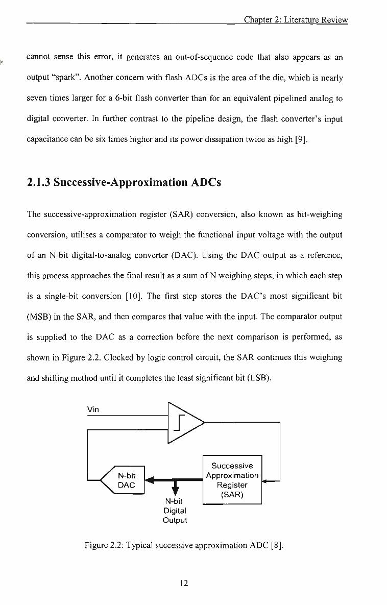
2.1.3 Successive-Approximation ADCs
The successive-approximation register (SAR) conversion, also known as bit-weighing
conversion, utilises a comparator to weigh the fiinctional input voltage with the output
of an N-bit digital-to-analog converter (DAC), Using the DAC output as a reference,
this process approaches the final result as a sum of N weighing steps, in which each step
is a single-bit conversion [10]. The first step stores the DAC's most significant bit
(MSB) in the SAR, and then compares that value with the input. The comparator output
is supplied to the DAC as a correction before the next comparison is performed, as
shown in Figure 2,2, Clocked by logic control circuit, the SAR continues this weighing
and shifting method until it completes the least significant bit (LSB).
Vin
N-bit DAC
N-bit Digital Output
Successive Approximation
Register (SAR)
Figure 2.2: Typical successive approximation ADC [8].
12

Chapter 2: Literature Review
As each bit is established, it is latched into the SAR as part ofthe ADC's output, SAR
converters consist of a comparator circuit, a DAC circuit, a SAR, and a logic confroller.
This type of conversion methods can sample at low data rates of only up to 1 Mega-
Samples-Per-Second (MSPS), use low supply current in the order of a few micro amps,
low power consumption of approximately 2mW and offer the lowest production cost in
the range of AUD$15 to AUD$600, The disadvantage of these designs is that their
analog design is demanding and time consuming,
2.1.4 Integrating ADCs
Integrating ADC technique, also known as dual-slope or multi-slope data converter, is
amongst the most popular converter types available. The standard dual-slope converter,
shown in Figure 2,3 [8, 11, 12], has two main sectors, which include a circuit that
attains and digitises the input, producing a time-domain interval, and a counter that
converts the result into a digital output code.
Switch-
w Switch, - V,fc i I 11.11 fc..
To Switch, & Switchj
Comparator
Oock
Figure 2,3: Dual-Slope hitegrating ADC [8]
13

Chapter 2: Literature Review
The dual-slope converter utilises an analog integrator with switched inputs, a
comparator, and a counter. The input voltage is integrated for a fixed time interval
(TCHARGE) that commonly corresponds to the maximum count of the internal counter, as
shown in Figure 2,4, At the conclusion of this interval, the device resets its counter and
applies an opposite-polarity to the integrator input. With this opposite-polarity signal
fiinctional, the integrator "de-integrates" until its output accomplishes zero. At this
stage, the counter is stopped and the integrator is reset. Charge that has been achieved
by the capacitor within the integrator during the first integrating/charging interval
'CHARGE
\v I V \'REF\ J
must equal that lost during the second, de-integrating/discharging
interval •'• CHARGE
\v I V y REF\ )
Under this condition the binary output is proportional to the ratio of
these time intervals.
••Time
*^ ' DISCHAR6E
Figure 2,4: Timing relationships for a dual-slope integrating ADC [8],
Integrating ADCs are particularly slow devices with low input bandwidth. However,
their ability to reject high frequency noise and fixed low frequencies, for example 60Hz,
makes these converters very usefiil in noisy environments [12],
14

Chapter 2: Literature Review
2.1.5 Sigma-Delta (E-A) ADCs
Sigma-delta (2-A) converters, also known as over-sampling converters have a
reasonably plain arrangement. They consist of a sigma-delta modulator, which is then
connected to a digital decimation filter, as shown in Figure 2.5 [14]. The modulator,
whose architecture is similar to that of a dual-slope ADC, includes an integrator and a
comparator with a feedback loop that contains a 1-bit DAC [13-15]. This internal DAC
is basically a switch that connects the comparator input to a reference voltage. The I-A
analog-to-digital converter also contains a clock that provides appropriate timing for the
modulator and digital filter [16, 17].
Integrator
Vs Comparator
OV
1-bit DAC
Digital Filter
Figure 2.5: Sigma-delta converter [14],
Low-bandwidth signals applied to the input of a S-A ADC are quantised with very low
resolution (1-bit), but require sampling frequencies greater than 2 MHz. Combined
with digital post-filtering, this over-sampling reduces the sampling rate to about 8 kHz
and increases the ADC's resolution to 16 bits or higher. Even though this type ofADC
is slower than the other described above, the standard of this converter has urbanised a
sturdy position in the ADC market.
15

Chapter 2: Literature Review
The E-A ADC offers three main advantages:
• Low-cost, high-performance conversion
• Integrated digital filter
• Digital Signal Processor (DSP) compatibility for system integration [14].
2.1.6 Pipeline ADCs
Due to the fact that pipeline ADCs provide an optimum balance of size, speed,
resolution, power dissipation, these ADCs topologies have become progressively more
eye-catching to data converter manufacturers and their designers [18-21], Also known
as sub-ranging quantisers, pipeline ADCs consist of several consecutive stages, each
containing a sample-and-hold (S/H) amplifier, a low-resolution ADC, DAC, and a
summing circuit that includes an amplifier to provide gain.
Applications for pipeline ADCs include communication systems, in which total
harmonic distortion (THD), spurious-free dynamic range (SFDR), and other frequency
domain specifications are relevant [8, 22-24], Another application ofthe pipeline ADC
is charged-coupled devices (CCD) based imaging systems, in which favorable time-
domain specifications for noise, bandwidth, and fast fransient response promising quick
settling. Pipeline ADCs are also used in data-acquisition systems, in which time and
frequency domain characteristics (i,e,, low spurs and high input bandwidth) are both
important [25, 26],
16
Chapter 2: Literature Review
2.1.6.1 Standard Architecture of Pipeline ADC
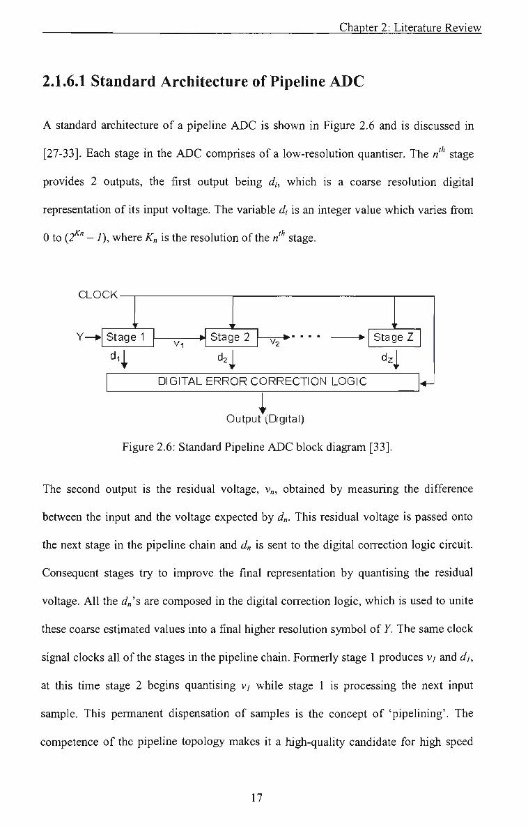
A standard architecture of a pipeline ADC is shown in Figure 2.6 and is discussed in
[27-33], Each stage in the ADC comprises of a low-resolution quantiser. The «"" stage
provides 2 outputs, the first output being di, which is a coarse resolution digital
representation of its input voltage. The variable di is an integer value which varies from
0 to (2 " - 1), where K„ is the resolution ofthe «"" stage.
CLOCK
Y-\ r
stage 1
d i |
^ ' V
h '-^t'^nri 9 ^ . . . . ^ "^tTr ,Q 7 w oLdyu z w ^ ^ o L j y i , 2_
d 2 | d z |
DIGITAL ERROR CORRECTION LOGIC ^
i Output (Digital)
Figure 2.6: Standard Pipehne ADC block diagram [33].
The second output is the residual voltage, v„, obtained by measuring the difference
between the input and the voltage expected by dn. This residual voltage is passed onto
the next stage in the pipeline chain and dn is sent to the digital correction logic circuit.
Consequent stages try to improve the final representation by quantising the residual
voltage. All the ^„'s are composed in the digital correction logic, which is used to unite
these coarse estimated values into a final higher resolution symbol of Y. The same clock
signal clocks all ofthe stages in the pipeline chain. Formerly stage 1 produces vy and di,
at this time stage 2 begins quantising v/ while stage 1 is processing the next input
sample. This permanent dispensation of samples is the concept of 'pipelining'. The
competence of the pipeline topology makes it a high-quality candidate for high speed
17

Chapter 2: Literature Review
and low power conversions. A one stage pipeline ADC block diagram is illusfrated in
Figure 2,7 and is discussed in several papers [34-37], A S/H amplifier is employed at
the input of each pipeline block. Each stage has a sub K„-hit ADC to provide the digital
output for that exact stage, A sub-DAC with comparable resolution to the sub-ADC is
utilised to convert the digital output back to an analog signal.
The analog signal is then subtracted from the initial sampled input, resulting in the
voltage error,/,. The consequential residual error/, is balanced by a gain factor and sent
to the following stage as v„. The gain usually has a value of (2^''-l), which depends on
the resolution of that particular stage. The gain factor is applied to scale the residual to
the fiill operating scale for the next stage. Choosing the gain as a power of two
extensively abridges the digital correction logic. Contravening the high-resolution
conversion into stages with low resolution has advantages and disadvantages. An
important advantage is a high conversion rate. Using pipeline block stages also saves
significant area, resulting in cost savings on silicon. If area is not a concern, more stages
can be added to acquire higher resolution.
S/H <5>
K„-bits
Sub^DC
' '
K^-bits
Sub-DAC
A
)Kn-1
d„(N„-bits)
Figure 2,7: Single Pipeline stage block diagram [37],
18
Chapter 2: Literature Review
2.1.6.2 Two-Stage Pipeline ADC Structure
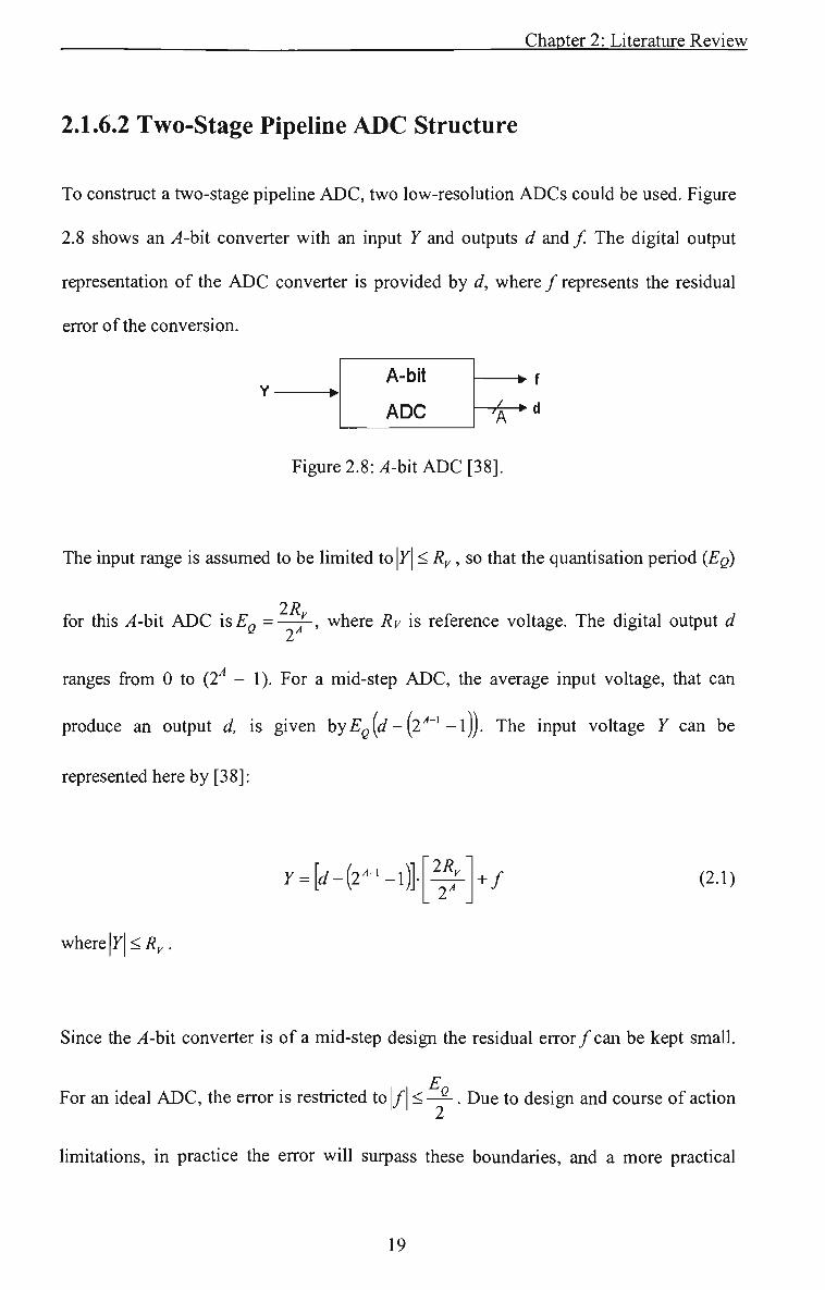
To construct a two-stage pipeline ADC, two low-resolution ADCs could be used. Figure
2,8 shows an .4-bit converter with an input Y and outputs d and / The digital output
representation of the ADC converter is provided by d, where / represents the residual
error ofthe conversion.
Y w
A-bit
ADC
h f • • 1
• fc H A * *•
Figure 2.8:/i-bit ADC [38].
The input range is assumed to be limited to |7| < i?^,, so that the quantisation period (EQ)
2R for this ^-bit ADC is Eg =—j^, where Ry is reference voltage. The digital output d
ranges from 0 to (2'^ - 1), For a mid-step ADC, the average input voltage, that can
produce an output d, is given hyEgyd-[2'^'^-Ij). The input voltage Y can be
represented here by [38]:
Y = [d-{2'-'-\)]-2R. + / (2.1)
where 7| < R„ .
Since the A-hii converter is of a mid-step design the residual error/can be kept small.
For an ideal ADC, the error is restricted to | / | < —^, Due to design and course of action
limitations, in practice the error will surpass these boundaries, and a more practical
19

Chapter 2: Literature Review
assumption would be|/ | < Eg. If/is available, a second ADC can be used to recover the
output by quantising this error.
A 5-bit converter is coimected at the output ofthe A-hit converter, as in Figure 2.9,
Y b
A-bit
ADC
^ ,
/ •d^
2 ^
A 1
> ^ B-bit
ADC
— •
- ^
Figure 2,9: Two-stage Pipeline ADC [38]
A gain factor is selected to make |v/| < Ry. Equation 2,1 can be written for the 5-bit
converter as.
2^.'l v.=k-(2--i)]-M^K/ 2"
(2.2)
w h e r e | / | < £ , = ^
However, since v, = 2 • / , therefore.
/,=k-(2'-'-l)]- 2R. "i r /, ^ iB+A-\ + tA-\
(2,3)
Using Equation 2,1, the A-hit converter output can be represented by [38]:
Out = \d, - ( 2 - - l ) ] - [ ^ ) + / , = ^ 2 - ' -(2'*^-^ - 2 - ' ) ) { ^ ) H - / , (2.4)
20

Chapter 2: Literature Review
By merging Equations 2,3 and 2,4, a term for the input Y and the quantised outputs can
be attained as [38]:
0«r = [r f ,2 ' -+ / , - (2- - - l ) ] . (^ + f2_
ryA-l (2,5)
The expression for Y in Equation 2,5 is in effect Equation 2.1, except it is written for a
single (B+A-l)-bit converter. By combining the two ADCs, a higher resolution
approximation ofthe input is obtained. The preferred digital output from Equation 2.5 is
given hyd -d^^2"~^ +d.^. The output d computation is carried out in the digital
correction logic of the topology. The quantisation period of the combined converter
is^, Q{B+A-\) 2*+-^-!
2/? 27? '' While 1/1 <—J-, the maximum error for the combined result is
restricted by / 2 , . 4 - 1
< 2R.
2^-2' T = EQf^g_^^_^^. The operation of the digital correction is to
calculate the final d for each sample by adding up all the stage outputs, d„. From the A-
bit and 5-bit representation, the concluding d is specified hyd^2"'^ +c?2 • ^^ ^^' ^^ ^
binary shift to line up the bits before transferring them to a binary addition. The outputs
are repositioned according to the resolution that each stage contributes to the final
estimate. Assuming d/ and d2 are divided into binary bits, Figure 2,10 shows the
configuration of these bits before the addition.
MSB
'A-l
(A+B-1)-bits
LSB
h h k ^B-1
d., is shifted by 2 -''
/ . / ,
Figure 2,10: Digital correction for (B +A - l)-bit ADC [38, 39],
21

Chapter 2: Literature Review
Notice that in Figure 2.10, // is the LSB and IA or IB is MSB ofthe consequent outputs.
The procedure of the ADC for input voltages > Ry needs meticulous consideration.
Analysis of the error correction logic shows that erroneous results are produced for both
d] = (2 - 1) and d2 = (2^ - 1). This conversion stipulation creates an arithmetic
overflow and cannot present a valid ADC output state. To resolve this setback, the
range of vaUd outputs for the A-hit converter is regularly limited.
Valid outputs vary from 0 to (2" - 2), thus this device will in no way create the
challenging output state (2 ^ - 1). In view ofthe fact that a mid-step design is practical
here, eliminating this output state will not degrade the performance of the converter.
The residual v„ will still satisfy the boundary |v„| < Ry provided that the input is
restricted hy \Y\< Ry. This will guarantee that the sample is predicted correctly and no
data is lost. The last stage of the pipeline ADC is only allowed to produce its diffusion
state d2 = 2^ - 1, This relationship corrects the saturation behavior of the converter, and
reduces the hardware required to implement all intermediate pipeline stages.
The number of stages in a pipeline ADC can differ. In the instance described previously,
the A-hit and 5-bit converters can be regarded as the 2 stages in (5+.^-/)-bit ADC. As
the resolution of a stage declines, the number of comparators needed for the entire
system also declines. An ^-bit stage can have up to (2' - 1) comparators to achieve a
resolution of yi-bits. Multiple stage pipeline ADC is what this research is concerned
about. By using this multiple stage philosophy, a reconfigurable pipeline ADC could be
constructed.
22

Chapter 2: Literature Review
2.1.6.3 Pipeline ADC with 1.5-bit/Stage
The requirements on the sub-ADC of a 1,5-bits/stage design are inhabited, hence
proficient high-speed designs can be structured. The 1.5-bits/stage only has three valid
quantisation periods, which are '00', '01'and '10'. In order to avoid overflowing in the
digital correction, the state ' 11' is not valid output, unless it comes from the last stage in
the pipeline string. To get ^-bits of resolution, (^ - 1) stages are required. Using this
characteristic architecture, the gain factor is set to a constant of 2 between the stages
[40, 41], A typical single stage structure ofthe 1.5-bits/stage architecture is illustrated in
Figure 2.11 and is described in several papers [42-45].
Y — • S/H < ^
Sub^DC
2
Sub-DAC
- •v„
Figure 2,11: Single stage, 1,5-bit/stage pipeline ADC [45],
D
Supposing that the input has a range of |7| < Ry, the quantisation period is -y. The
D D
sub-ADC should have thresholds of —^ and ^. hi practice, the definite ADC
4 4
thresholds will be different from these 'nominal' values. The ADC thresholds are
illusfrated in Figure 2.12 [38, 39], Figure 2,12 also illusfrates the corresponding digital
outputs of the sub-ADC and the analog voltages, which are produced by the sub-DAC,
The digital word-length is propelled to the digital correction logic of the ADC to be
23

Chapter 2: Literature Review
amalgamated with all the other outputs from the other stages. The digital output delivers
the input to the sub-DAC, This sub-DAC is designed to produce one of three possible
output voltages. For the 1.5-bits/stage architecture these voltages are set to —^, 0, and
D
— - for sub-ADC outputs codes '00', '01' and '10' respectively. The sub-DAC output
is deducted from the input and the residual voltage is amplified by a gain factor of 2. If
the sub-DAC outputs are accurate, this gain factor will level the residual error to ±Ry,
D
provided the sub-ADC quantisation thresholds are within —^ of their nominal values.
The subsequent stage will then quantise the residual error from this stage.
ADC Thresiiolds (Actual)
-Rx.
00
Rv
<'Y
ADC Thresholds (Nominal) 10
- H *
Digital outputs
# Represents the DAC "00", "01", "10" digital outputs
Figure 2,12: Sub-DAC outputs, 1,5-bit/stage pipeline ADC [38].
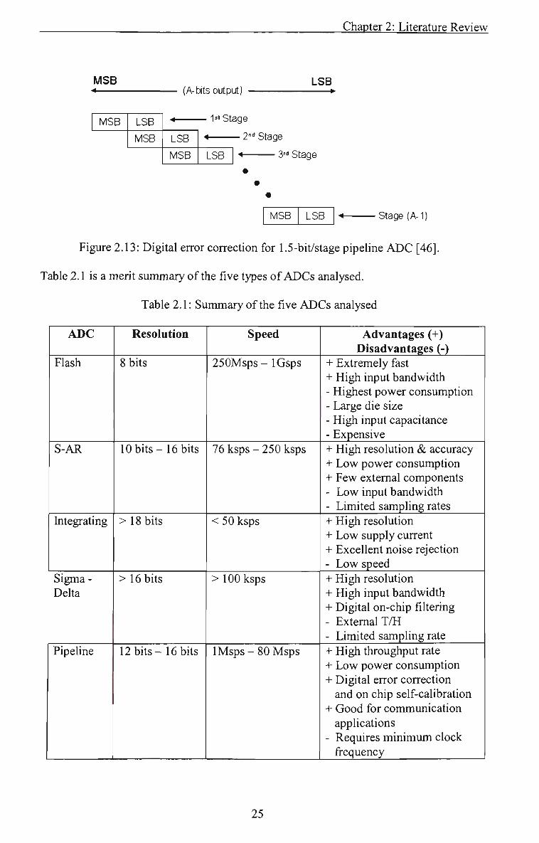
Digital error correction for a 1.5-bits/stage pipeline ADC is simple. Tentatively, the first
stage in a pipeline presents the MSB for the final output and the last stage presents the
LSB. Figure 2.13 [46] illusfrates how the bits from each stage are joined together.
24
Chapter 2: Literature Review
MSB (A-bits output)
LSB
MSB LSB
MSB
1« Stage
LSB
MSB
2"" Stage
LSB S'" Stage
MSB LSB * Stage (A1)
Figure 2.13: Digital error correction for 1,5-bit/stage pipeline ADC [46].
Table 2,1 is a merit summary ofthe five types of ADCs analysed.
Table 2.1: Summary ofthe five ADCs analysed
ADC
Flash
S-AR
Integrating
Sigma-Delta
Pipeline
Resolution
8 bits
10 bi ts -16 bits
> 18 bits
> 16 bits
12 bi ts -16 bits
Speed
250Msps-lGsps
76 ksps - 250 ksps
< 50 ksps
> 100 ksps
IMsps - 80 Msps
Advantages (+) Disadvantages (-)
+ Extremely fast + High input bandwidth - Highest power consumption - Large die size - High input capacitance - Expensive + High resolution & accuracy + Low power consumption + Few external components - Low input bandwidth - Limited sampling rates + High resolution + Low supply current + Excellent noise rejection - Low speed + High resolution + High input bandwidth + Digital on-chip filtering - External T/H - Limited sampling rate + High throughput rate + Low power consumption + Digital error correction
and on chip self-calibration + Good for communication
applications - Requires minimum clock
frequency
25

Chapter 2: Literature Review
Literature on existing reconfigurable ADCs clearly differs from the work presented in
this thesis. The work performed in [47], is one of these existing literatures. The design
performed in [47] takes an approach where the user defines the resolution, and then
depending on the selected resolution a particular ADC structure is selected, such as
Sigma-Delta ADC or a pipeline ADC, Also the work performed in [47] is only on the
architecture of the ADCs, not particularly selected for an application. However, one of
the most important aspects of the difference between the work presented in this thesis
and the design in [47] is that the design in [47] is not a real-time reconfiguration. The
proposed reconfigurable architecture in this thesis is fiilly real-time reconfigurable
design, where depending on the interference occurring from adjacent base and mobile
stations, the ADC, in real-time, by using an intelligent control unit, reconfigures it self
to meet the required specification.
PART II
2.2 Wideband Code Division Multiple Access
Second generation systems (2G) such as personal digital communications (PDC), global
system for mobile communications (GSM), cdmaOne (IS-95) and US-time division
multiple access (TDMA) (IS-136) have enabled voice communication to switch to
wireless. Also known as digital systems, they offer services such as text messaging and
access to data networks. Prior to this second generation of systems, the analog cellular
systems referred to as the first generation systems (IG) were in use. Lacking quality for
multimedia communications (person to person communication) and access to
information and services on public and private networks ofthe IG and 2G, the third
generation systems (3G) were designed. With the continuous evolution of the 2G and
the design of the 3G, new business opportunities for the manufacturer and the provider
using these networks have been created. Wideband code division multiple access
(WCDMA) technology has been surfaced as the most extensively accepted third
26

Chapter 2: Literature Review
generation air interface. The joint standardisation bodies from Japan, China, Europe,
USA, and Korea have created the specification for WCDMA in the third generation
partnership project (3GPP), Within this partnership project, WCDMA is referred to as
the Universal Terrestrial Radio Access (UTRA), WCDMA is characterised by two
duplex modes: Frequency Division Duplex (FDD) and Time Division Duplex (TDD)
[48], Figure 2,14 [48, 49] illusfrates the peculiarity between the two duplex modes. The
space division duplex (SDD) method is not considered here because this method is used
in fixed-point transmission where directive antennas can be used. This method is not
used in mobile terminals.
• ^ Bandwidth =5 MHz
Downlink 1
1 •
Uplink
\ Guard Period
Time Bandwidth = 5 MHz
Frequency
TDD
Separation Duplex 190 MHz —
FDD
Figure 2,14: UTRA duplex modes [48, 49],
In the UTRA-FDD mode, the uplink and downlink transmissions use paired radio
frequency bands whereas in UTRA-TDD, uplink and downlink transmissions are
carried over same radio frequency using synchronised time intervals. Time slots in the
physical channel are divided into transmission and reception part [50-52], Information
on uplink and downlink are fransmitted reciprocally [53]. This makes TDD mode
susceptible to adjacent channel interference (ACI) as nearby mobile stations (MS) and
base stations (BS) cause interference to each other depending on frame synchronisation
27

Chapter 2: Literature Review
and channel asymmetry. Table 2.2 [54] compares the key parameters of the UTRA-
TDD and FDD physical layer.
Table 2,2: Parameters comparison of UTRA-TDD and FDD
Duplex Method Multiple Access Method
Channel Spacing Carrier Chip Rate Timeslot Structure
Frame Length Modulation
Multirate Concept Intra-Frequency Handover Inter-Frequency Handover
Spreading factors
UTRA-TDD TDD
TDMA, CDMA, FDMA
UTRA-FDD FDD
CDMA (inherent FDMA) 5 MHz (nominal)
3,84 Mcps 15 slots/frame
10 ms QPSK
Multicode Hard Handover
Multicode and OVSF Soft Handover
Hard Handover 1 .,. 16 4 . . .512
The reconfigurable pipeline ADC is designed to be used on the downlink UTRA-TDD
mode due to its near far problem. The near far problem along with the interference
issues is described in section 2,2,2,3 of this chapter. Under this condition, the UTRA-
TDD mode is described in greater detail in the following section,
2.2.1 UTRA-TDD Mode
There are distinct advantages of the UTRA-TDD system in comparison to the FDD
system. The key advantage is that the TDD system can be implemented on an unpaired
frequency band, while the FDD system requires a pair of bands. This characteristic
solves some frequency band allocation issues resulting in effective and efficient use of
the spectrum [54, 55], Services such as mobile hitemet, multimedia applications and file
fransfers may have different capacity requirements for uplink and downUnk
fransmission, UTRA-TDD offers the advantages of flexibility in resource allocation, as
28
Chapter 2: Literature Review
the frequency band is not fixed between uplink and downlink [54, 55], Other advantages
ofthe TDD system are listed in [56] and include the following:
Adaptive support of asymmetric data rates
High speed data services for indoor or low-mobility operating environments
Large channel capacity (equivalent to FDD mode)
Small sized mobile terminal
Low complexity transceivers
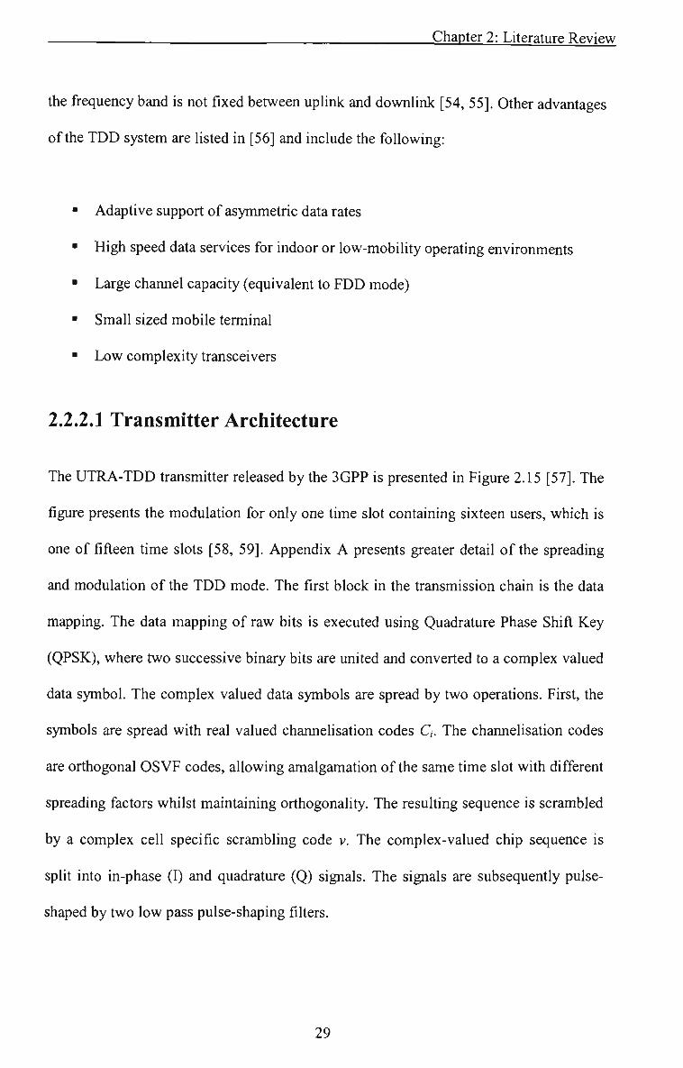
2.2.2.1 Transmitter Architecture
The UTRA-TDD transmitter released by the 3GPP is presented in Figure 2,15 [57], The
figure presents the modulation for only one time slot containing sixteen users, which is
one of fifteen time slots [58, 59], Appendix A presents greater detail ofthe spreading
and modulation of the TDD mode. The first block in the transmission chain is the data
mapping. The data mapping of raw bits is executed using Quadrature Phase Shift Key
(QPSK), where two successive binary bits are united and converted to a complex valued
data symbol. The complex valued data symbols are spread by two operations. First, the
symbols are spread with real valued channelisation codes C,. The channelisation codes
are orthogonal OSVF codes, allowing amalgamation ofthe same time slot with different
spreading factors whilst maintaining orthogonality. The resulting sequence is scrambled
by a complex cell specific scrambling code v. The complex-valued chip sequence is
split into in-phase (I) and quadrature (Q) signals. The signals are subsequently pulse-
shaped by two low pass pulse-shaping filters.
29

Chapter 2: Literature Review
User 1 Useri (Maxi= 16)
_i 1 QPSK
I QPSK
c , ^ c , ^
Cell Specific Scrambling Code ( v ) - > / \
[cos(ft*)]—»•(>< 2 GHz
Complex-Value Chip Sequence (S)
Xj^[-sm(at)] 2 GHz
Figure 2,15: UTRA-TDD Base band Transmitter (one time slot) [57]
The two DACs after the pulse-shaping filters, convert the digital signals to analog
signals. The signals are afterwards quadrature modulated to characterise the signal in
RF format at the 2 GHz carrier frequency. The whole information is enclosed in the
complex envelope and in the phase ofthe RF signal.
2.2.2.2 Receiver Architecture
Figure 2,16 [57] illusfrates the standard block diagram of a direct conversion UTRA-
TDD receiver. A RF signal is received by the antenna and then processed by the RF
filter and the low noise amplifier (LNA). The quadrature demodulator produces a
30

Chapter 2: Literature Review
complex valued chip sequence, both I and Q, The anti-aliasing filter removes aliasing in
the spectrum from both I and Q then the ADC converts the signal from analog to digital.
The RRC filter has a pulse-shape impulse response that attenuates out-of-band signals
from the I and Q channels before the in-band signal is brought to the other base band
signal processing blocks. The end user of the mobile terminal will experience a great
deal of interference noise if the out-of-band signals were not filtered. Once filtering is
completed, the signals are de-scrambled with a cell specific scrambling code V„, de-
spread with chaimelisation code, and finally de-modulated (de-QPSK) to obtain the
users' raw data bits,
Out-of-Band
In-Band
fMc-^i'^ De-
scramble
OSVF„
De-spread De-mod data,
Figure 2.16: UTRA-TDD Receiver architecture for one time slot [57]
2.2.2.3 Interference Issues (Downlink Analysis)
This section describes the adjacent channel interference (ACI) experienced at the mobile
terminal, where the signals arrive from the base stations, also known as downlink
analysis. Due to the fact that the Analog-to-Digital Converter is within the mobile
receiver (Ms), and the signals are sent from the BS to MS, it is appropriate to analyse
and review the downlink propagation ofthe signals arriving at the MS, Two interference
instances exist in this scenario, mobile station to mobile station (MS^MS) and base
station to mobile station (BS->MS) interference.
31

Chapter 2: Literature Review
2.2.2.3.1 Propagation Model
The path loss is modelled in accordance to the COST 231 indoor propagation
environment with no wall and floor losses [60-62]:
H: = 31 + r\0\og(d) + [dB] (2,6)
where / is the path loss exponent and d is the separation between fransmitter and
receiver. Lognormal shadowing is modelled by ^ [60] with a mean of zero and a
standard deviation of a. The receiver sensitivity is modelled as:
Rs=—+?7-pg + I^^rgin [dB] (2,7)
where Eb/No is the required bit-energy to interference ratio, t] is the thermal noise, pg is
the processing gain and Imargin is an additional interference margin from the presence of
other users in the same cell. Imargin is modelled as:
r 1 -'margm ^ _- j ( 2 . 8 )
Pg Eb/No
where M is the number of users in the cell of interest (COI). Transmission power (Ptx)
is derived from the receiver sensitivity Rs and the path loss model K and is as follows:
32
Chapter 2: Literature Review
Ptx = Rs + K [dB] (2.9)
2.2.2.3.2 Downlink Interference Model
The extent of this work was restricted to downlink analysis. As noted earlier, MSs
experience ACI from two sources, adjacent BSs and adjacent MSs dependant on the
synchronisation factor a. To gain an understanding of how this affects the amount of
ACI experienced from BSs and MSs, we need to examine toff. A small toff results in a
high BS->MS interference and a low MS->MS interference. It is vice versa for a large
toff. It cannot be assumed that synchronised frames in a fiilly flexible system, therefore
the computer simulations take into consideration misaligned frames and different
asymmetry. To explore the effect of ACI in the downlink with no adjacent charmel
protection (ACP) factor present, it would give the raw adjacent channel interference
power. These raw adjacent interference power measurements are needed to determine,
depending on location in the COI, how much ACP is needed to satisfy the required bit
energy to interference ratio (Eb/No).
To determine the interference power from a single adjacent channel BS at a MS in the
COI, we need to first determine the adjacent channel BS fransmission power and the
path loss between this BS and the MS in the COI, The ACI is then the BS transmission
power multiplied by how many users are being served in this adjacent channel cell, over
the path loss and is as follows:
_Ptx,^*M IBS- (2,10)
33

Chapter 2: Literature Review
where IBS is the interference experienced from the adjacent base stations, PtXbs is the
adjacent channel BS transmission power, M is the number of users served by this BS,
and Kbs is the path loss between the adjacent channel BS and the MS in the COI, Based
on this model, the total raw BS->MS ACI can be calculated with many adjacent channel
interferers. Hence, raw BS^MS adjacent channel interference including a
synchronisation factor is modelled by [62]:
" Ptx^MJ IB=ZU(}-^)—-J (2,11)
y=l '^ 5.
where IB is the raw adjacent channel interference experienced from MS -> BS, K:^B„ is
the path loss between they"" adjacent channel BS causing interference and the mobile
located at m in the COI, M^ is the number of users served by the/^ BS. Ptx' is the/**
adjacent BS fransmission power. The user facing the greatest attenuation in an adjacent
channel cell determines the transmission power of that adjacent channel BS. This results
in high or low BS fransmission powers.
To investigate the interference power from a single MS in one adjacent channel cell at a
MS in the COI, the transmission power ofthe MS in the adjacent channel cell needs to
be calculated. The path loss from the adjacent channel MS to the MS in the COI also
need be determined. The ACI results in:
Ptx IMS=^^^^ (2.12)
34

Chapter 2: Literature Review
where IMS is the interference experienced from the adjacent mobile stations, PtXms is the
adjacent channel MS transmission power and Xms is the path loss between the adjacent
channel MS and the MS in the COI, To investigate the raw MS->MS ACI caused by
many MSs in many adjacent channel cells incorporating a synchronisation factor, the
interference results in [62]:
H M pj
^A/=ZZ^ j ""' (2.13)
where IM is the raw adjacent channel interference experienced from MS -> MS,
K^MtM,„ is the path loss between the /"' MS in the f^ adjacent channel cell causing
interference and the mobile m in the COI. PtXi is the MS transmission power. It can
clearly be seen that when a = 0, all ACI is sourced from the adjacent BSs, If a = 0,01,
this would mean that ninety nine percent of ACI is from adjacent channel BSs and one
percent from adjacent channel MSs, The total ACI is a linear sum of both sources of
interference. Therefore, the total downlink raw ACI power a mobile experiences at point
m is:
Itotal=h+lM (2.14)
2.3 Conclusion
There are distinct advantages of using the pipeline ADC topology as compared with
other topologies such as Flash ADCs, SAR ADCs, Sigma-Delta ADCs and Integrating
ADCs, While the flash ADC architecture can reach very high speed, it consumes a lot of
35

Chapter 2: Literature Review
power due to the high cfrcuit complexity and large device count. The other ADC
architectures consume little power, but they operate at very low speeds, which are not
appropriate for the UTRA-TDD application, where the 3G specification of 15,36 MSPS
needs to be met. However, even though fix word-length pipeline ADC architecture
could be a suitable device for the mobile receiver, it still has a distinct disadvantage
when it comes to power consumption. In many cases a fixed word-length ADC is used,
say 12-bits, when the receiver requires and uses a converter of only 8-bits, During this
time the whole 12-bit device is powered up, which uses a lot more power than it is
supposed to. To achieve this, a more complex receiver ADC design and implementation
is required, which will have a significant impact on battery life in the mobile terminal.
ADC optimisation techniques could lower power consumption but will not reduce it to
its most efficient level. A solution in theory is to use minimum resolution, and still meet
the performance requirements of the UTRA-TDD receiver specified by the 3GPP, To
achieve this, in-band and out-of-band signal powers need to be measured. Then the
ADC intelligently chooses the amount of resolution required to ensure the out-of-band
signal is below a certain tolerance level and the SNR is met. This scheme will reduce
power consumption, as it only utilises the required resolution as compared to traditional
fixed complexity architectures.
To translate theory into reality, the solution has to take advantage of the software radio
concept and technologies [54], An exact definition for a software radio does not yet
exist, but there are many definitions to help gain an understanding [55, 56].
36

Chapter 2: Literature Review
Taking advantage of the software radio theory, a solution can be achieved using DSP
and application specific integrated circuit (ASIC) technologies that can meet the
performance and system needs of high speed and low cost devices. A DSP can interface
with an ASIC and control the ADC resolution dependant on in-band and out-of-band
power ratios, making the design a reconfigurable solution. This could be embedded on a
single chip to provide a System on a Chip (SoC) solution.
37
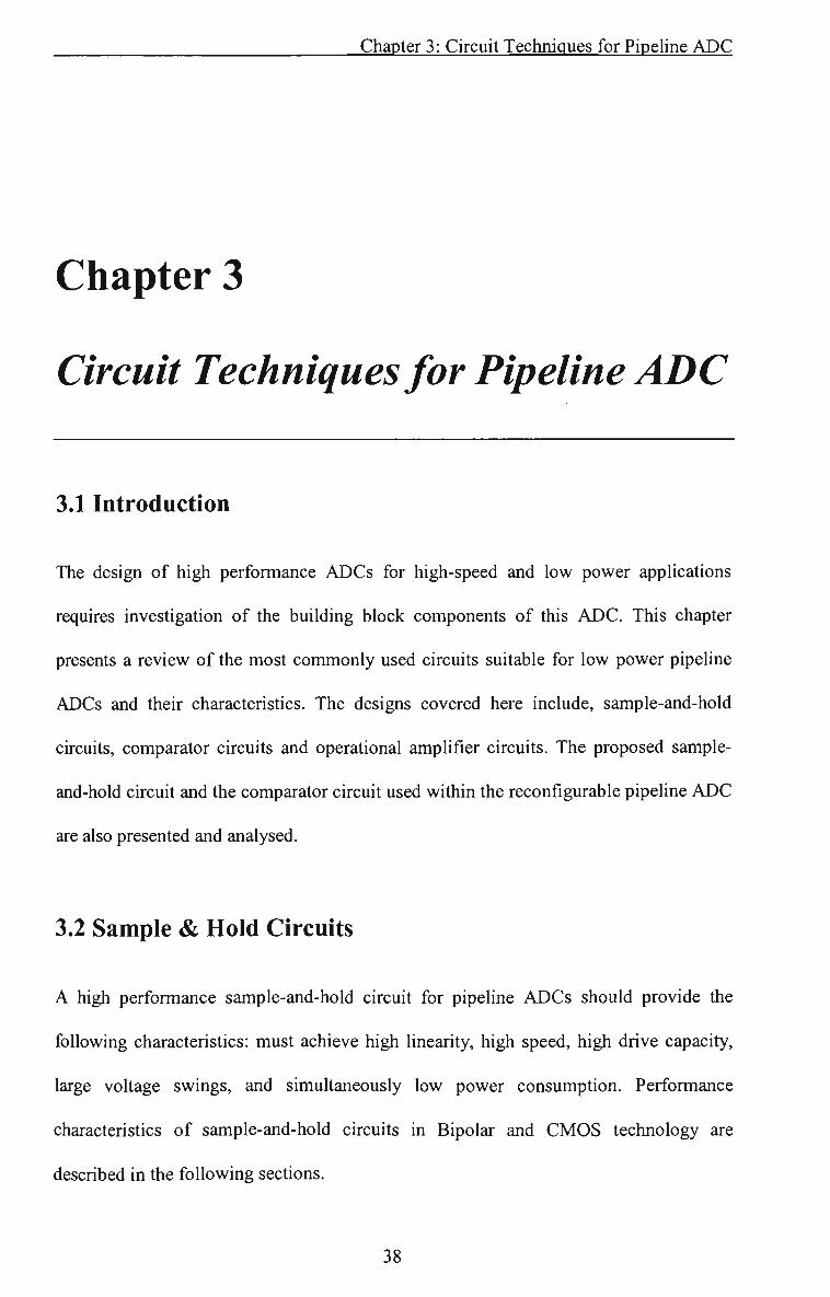
Chapter 3: Circuit Techniques for Pipeline ADC
Chapter 3
Circuit Techniques for Pipeline ADC
3.1 Introduction
The design of high performance ADCs for high-speed and low power applications
requires investigation of the building block components of this ADC, This chapter
presents a review of the most commonly used circuits suitable for low power pipeline
ADCs and their characteristics. The designs covered here include, sample-and-hold
circuits, comparator circuits and operational amplifier circuits. The proposed sample-
and-hold circuit and the comparator circuit used within the reconfigurable pipeline ADC
are also presented and analysed.
3.2 Sample & Hold Circuits
A high performance sample-and-hold circuit for pipeline ADCs should provide the
following characteristics: must achieve high linearity, high speed, high drive capacity,
large voltage swings, and simultaneously low power consumption. Performance
characteristics of sample-and-hold circuits in Bipolar and CMOS technology are
described in the following sections.
38
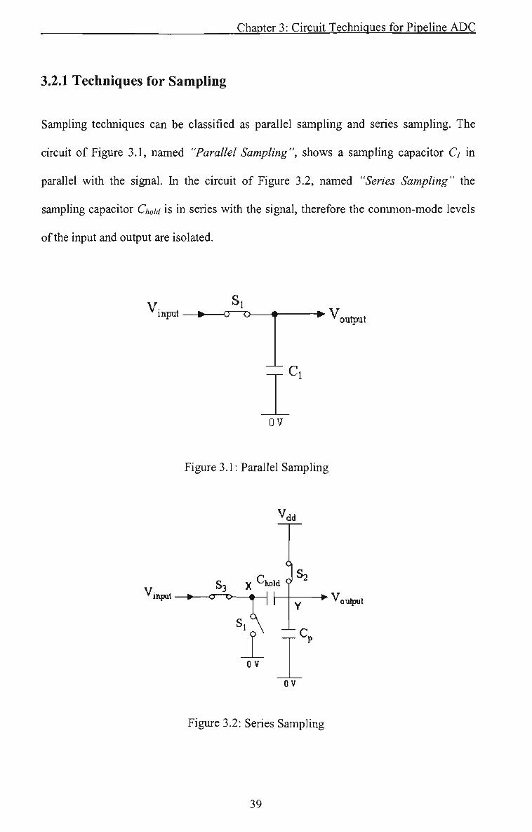
Chapter 3: Circuit Techniques for Pipeline ADC
3.2.1 Techniques for Sampling
Sampling techniques can be classified as parallel sampling and series sampling. The
circuit of Figure 3.1, named "Parallel Sampling", shows a sampling capacitor C; in
parallel with the signal. In the circuit of Figure 3.2, named "Series Sampling" the
sampling capacitor Choid is in series with the signal, therefore the common-mode levels
ofthe input and output are isolated.
v. 1 input — ^ C5—O-
^ V output
_ C i
OV
Figure 3.1: Parallel Sampling
'dd
S3 X »"W ^ ^ input — • o—o— •*v, output
OV
OV
Figure 3.2: Series Sampling
39

Chapter 3: Circuit Techniques for Pipeline ADC
In Figure 3.2, while the acquisition stage, switches S2 and S3 are on and in the fransition
to the hold mode, first node Y is released from Vdd and subsequently node X is shorted
to ground, producing a voltage charge at the output equal to the value of the input. The
"Series Sampling" technique has a great advantage over the "Parallel Sampling"
technique. Whilst parallel samphng endures from input dependent charge injection of
Si, series sampling doesn't demonsfrate such behavior due to the fact that S3 turns off
after S2, therefore injecting a constant charge onto node Y.
The "Series Sampling" technique has two disadvantages compared to the "Parallel
Sampling" technique. The non-linearity of the parasitic capacitance Cp at point Y
introduces distortion in the sampled value, consenting that the value of Choid be
adequately larger than that of Cp. Also, the hold settling time in series sampling is a lot
longer than in parallel sampling.
This is due to the fact that in the past the output voltage (Voutput), niust always begin
from a reset value while in the concluding stage, Voutput begins from a level close to its
finishing value. Sampling techniques could be implemented with various types of
switches. One of these types is by using MOS transistors, as shown in Figure 3,3,
MOS fransistors need low complexity and trouble-free circuitry but they reveal two
sources of dynamic errors, totaling to the channel charge injection and clock feed-
through. First, as shown in Figure 3,4, the finite fransition time ofthe sampling clock
consequences in an input dependent sampling instant [63].
40

Chapter 3: Circuit Techniques for Pipeline ADC
Figure 3.3: A typical CMOS switch [63]
Voltage
'ax
CLK
Ideal Sampling
fostant Vjapo, + VxH
Actual Sampling
Instant - • t
Figure 3,4: Input dependent sampling stage [63].
Second, as illusfrated in Figure 3.5, the disparity of the switch on-resistance with the
input level institutes distortion.
^lnj/!^^^\ffoo high
Figure 3,5: Distortion due to disparity of switch on-resistance [69],
Another issue that must be considered when designing in low voltage applications is the
high on-resistance of the actual MOS devices, in particular when the source/drain
41

Chapter 3: Cfrcuit Techniques for Pipeline ADC
common mode level is approximately YiVdd [69]. The design of low-voltage analog and
mixed signal circuits often imposes severe speed and precision limitations upon signal
processing systems. In multi-step ADC, such as the pipeline topology for example, the
front-end sample-and-hold amplifier must achieve high speed and high linearity with
low power consumption while the limited voltage headroom contains its dynamic range.
It is recommended that in pipeline ADC, series sampling to be used instead of parallel
sampling. This is because the parallel sampling suffers from input dependent charge
injection, where as series sampling does not illustrate such behavior.
3.2.2 Sample & Hold Circuits in Bipolar technology
In bipolar technology the simphfied sampling bridge of Figure 3.6 is used [63].
Achieving a high speed, the circuit nevertheless provides little dynamic range with a 3-
volt supply. Alternatively, the bridge can be modified as illustrated in Figure 3.7, where
the top two diodes are removed, the input diode is replaced with an emitter follower,
and the bottom current source is converted to a single-ended form, saving some voltage
headroom.
CLK
*-v, output
hold
Figure 3.6: Simphfied diode bridge [63].
42
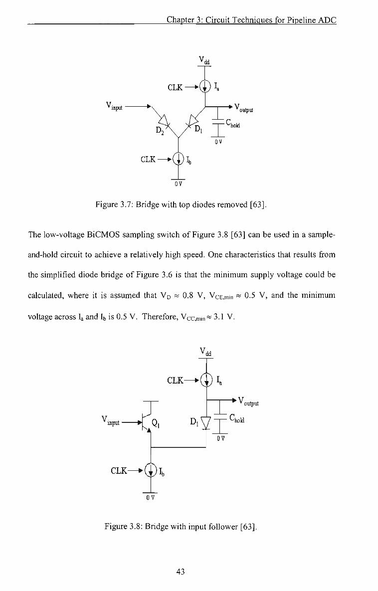
Chapter 3: Cfrcuit Techniques for Pipeline ADC
C L K - * ( i ) 4
OV
Figure 3.7: Bridge with top diodes removed [63].
The low-voltage BiCMOS sampling switch of Figure 3.8 [63] can be used in a sample-
and-hold circuit to achieve a relatively high speed. One characteristics that results from
the simplified diode bridge of Figure 3.6 is that the minimum supply voltage could be
calculated, where it is assumed that VD « 0.8 V, VcE,min « 0.5 V, and the minimum
vohage across la and lb is 0.5 V. Therefore, Vcc.min » 3.1 V.
V, dd
CLK—•( (t);
V input \ . Qi
• > v „ I '' * output
CLK—•O)] ,
wx' 'hold
OV
OV
Figure 3.8: Bridge with input follower [63].
43

Chapter 3: Circuit Techniques for Pipeline ADC
3.2.3 Sample & Hold Circuits in CIMOS technology
Sample-and-hold (S/H) circuits' architecture that is popular in CMOS technology is
shown in Figure 3.9, The design here is based on the series sampling technique, shown
in Figure 3,10, The approach illustrated in Figure 3,9 utilises a virtual ground to
perform a precise previous fiinction. Since at the end ofthe acquisition mode, Sj and S2
tum 'off after S3 and S4, the charge injected by the former two is equal, distributing
only the output Common Mode (CM) level. The difficult task however here is in the
design ofthe operational amplifier used in this technique.
V •o - 'o -
S5
- 0—0-
input
S2
+ > 'output
S4
S6
Figure 3.9: Unity gain sampling [64]
OV
input
6
\ Si 1 c,
-i—ft 1 1 •5^° 1 1 ,<
1 1 ' <r-^ —1 h—
>
3
C3
1 1 1 1
+ - v.. .6 '
1 1 1 1 C4
output
OV
Figure 3,10: Series sampling technique [64]
44

Chapter 3: Circuit Techniques for Pipeline ADC
More specifically:
• As the supply voltage of the op-amp is reduced, the op-amp suffers from
various frade-offs in dynamic range, speed, and linearity,
• The op-amp needs an input/output common-mode level approximately equal
to half the supply voltage, therefore limiting the gate-source overdrive
voltage of ^5 - S6 and degrading the settling behavior.
The circuit of Figure 3,9 only produces a maximum sampling frequency of 25 MHz
[64]. This can be partly attributed to the large device widths required in the op-amp so
as to achieve adequate voltage swings. Due to this reason, the architecture shown in
Figure 3.10 is suitable in a way that it allows independent choice ofthe input and output
common mode (CM) levels. Figure 3.11 illustrates a S/H circuit architecture proposed
in [65],
input + ^
CLK
+ T
—<^
« — • •
G2 + +
hold V, output
CLK
Figure 3.11: S/H architecture with transconductance and fransresistance stages [65],
The circuit employs a transresistance stage R and two transconductance stages, Gj and
G2, where GiR=G2R = 1- When the circuit is in the acquisition period, the combination
of Gi and R operate as a unity amplifier in which the output voltage Voutput is allowed to
45

Chapter 3: Cfrcuit Techniques for Pipeline ADC
track the input voltage Vi„put. When the circuit is in the hold period, the
transconductance G2 is enabled, Gj is disabled, and G2 and R are configured as a unity
gain amplifier in which the sampled value of Vi„put retained across capacitor Choid-
Another S/H circuit architecture similar in operation to the topology of Figure 3,11 with
is the recycling S/H circuit illustrated in Figure 3,12 [66],
input oiiput
Figure 3,12: Recycling S/H circuit architecture [66],
During the sample stage ofthe operation, Sj, S2 and S3 are switched on and the G stage
creates an implicit ground at point X, While the fransition from sample to hold mode
takes place, S3 turns off first, concurrently Sj and S2 tum off, and S4 turns on.
Therefore, Aj, A2 and G make up a unity gain feedback loop, which would hold the
samphng level on Ci,
3.2.3.1 Switched Capacitor Sample & Hold Circuits
Switched capacitor circuits are pervasive in highly integrated, mixed signal applications.
The sample-and-hold is the most basic and ubiquitous switched-capacitor building
block. Before a signal is processed by a discrete-time system, such as an ADC, it must
46

Chapter 3: Circuit Techniques for Pipeline ADC
be sampled and stored. This often greatly relaxes the bandwidth requirements of
following circuitry, which now can work with a DC voltage.
Due to the fact that the S/H is often the first block in the signal processing chain, the
accuracy and speed of entire application cannot exceed that ofthe S/H,
3.2.3.1.1 Top Plate Sample-and-Hold Circuits
In CMOS technology, the simplest S/H consists of a MOS switch and a capacitor as
shown in Figure 3,13 [67]. When Vg is high the NMOS transistor acts like a linear
resistor, allowing the output Vo to track the input signal Vj. When Vg transitions low,
the transistor cuts off isolating the input from the output, and the signal is held on the
capacitor at VQ.
M r J.
v„
Figure 3,13: MOS Sample-and-Hold [67]
There are several practical limitations to this circuit. Because the RC network has finite
bandwidth, the output cannot instantaneously track the input when the switch is
enabled. Therefore, a short acquisition period must be allocated for this (exponentially
decaying) step response.
47

Chapter 3: Circuit Techniques for Pipeline ADC
After the S/H has acquired the signal, there will be a fracking error due to the non-zero
phase lag and attenuation of the sampling network. The latter linear, low-pass filtering
does not introduce distortion and is usually benign for most applications,
3.2.3.1.2 Bottom Plate Sample-and-Hold Circuits
A technique called bottom-plate sampling to first order eliminates some of the errors in
the top-plate S/H circuit. Figure 3,14 shows the bottom-plate sampling configuration.
While clocks ^' and ^are high, Vo fracks the input voltage F,. When clock ^' transitions
from high to low, switch M2 turns off, and the charge on node X is trapped. The charge
on capacitor C is now fixed q=CVi. This is the defined sampling instant. When ^ clock
transitions from high to low, switch Mi is turned off and the output is isolated from the
input [67, 68],
J-g—Ih-h
1
Z^"
Figure 3.14: Bottom plate sample-and-hold circuit [67]
When M2 turns 'off, the voltage at node X is perturbed due to clock feed through and
charge injection. In this case, the charge injection is signal-independent because drain
and source see a fixed potential (ground). This condition eliminates signal-dependent
charge injection distortion.
48

Chapter 3: Circuit Techniques for Pipeline ADC
The charge injection from Mj does not alter the charge stored on capacitor C due to
charge conservation.
3.2.4 IMethods of using S/H circuits in ADCs
Using a front-end sample-and-hold circuit in ADC architecture is highly valuable in
some cases, but very much unnecessary in other cases. Some common applications are
considered below.
3.2.4.1 One-Stage & IMulti-Stage ADCs
The need of front-end sample-and-hold circuits in ADCs is highly beneficial. This is
due to the fact that one-stage ADCs, such as folding and flash topologies use a
distribution of samples in the cache of comparators. On the other hand, some not so
ideal timing issues in these architectures restrain the effective number of bits at high
input frequencies. A lot of apparatus report for this squalor [63]. Firstly, as illustrated
in Figure 3.15, the non-linearity noticed on the input capacitance, which occurs from a
large number of comparator circuits together with the source impedance resulting in a
harmonic distortion.
-fx • ^
.Oi Q:
' i - ^
P-
Pi
Figure 3,15: Non-linearity of input capacitance in Flash ADC [63]
49

Chapter 3: Circuit Techniques for Pipeline ADC
Secondly, as depicted in Figure 3.16, an input dependent offset from each comparator
circuit is introduced by the capacitive feedback from the input signal to the ladder of
resistors disturbing the reference stage voltages.
V; input
1
M, Mo
Q
R,
i t — •
R. T
GV
Figure 3.16: Feedback of input signal to resistance ladder [63]
Thirdly, as shown in Figure 3.17, sparks appear in the thermometer code of a flash ADC
due to mismatches between different sampling instants of neighboring comparator
circuits.
_^^ /-t-a Sampled by^/*i
J > > — 0
Samptod by Aj
Figure 3.17: Bubbles (sparks) appearing from timing disparity [63].
50
Chapter 3: Circuit Techniques for Pipeline ADC
3.3 Comparator Circuits
The design of fast precision comparators require careful trade-offs among parameters
such as speed, resolution, power consumption, and input capacitance. The speed of a
comparator is often limited by its preamplifier override recovery, while the resolution is
constrained by the input offset of its latch, A CMOS comparator utilising offset
cancellation technique has been introduced in this section. To achieve a small residual
offset, this technique combines a preamplifier and a regenerative latch, both with an
offset cancellation. Also in this section a design and simulated results have been
presented of a CMOS comparator used in an interleaved pipeline ADC that performs
analog processing only by means of open-loop circuits to achieve high conversion rate.
To achieve the correct residual output from one-stage pipeline ADC, an amplifier circuit
is employed to amplify the output, so it is equal to the original input. This amplification
factor is 2^, when N is the number of bits required. This section introduces a number of
comparator design techniques for use in ADC that are implemented in CMOS very large
scale integration (VLSI) technologies, in particular attention is paid to offset
cancellation techniques. The suggested techniques are intended to provide improved
speed and resolution while maintaining low power consumption and low complexity,
3.3.1 Offset Cancellation Techniques
3.3.1.1 Circuit Topologies
Of the various offset cancellation techniques, two of the most common approaches,
based on input offset storage (lOS) and output offset storage (OOS) are illusfrated in
Figure 3.18 and 3.19. The two approaches are design to be fimctional to a fiilly
51

Chapter 3: Circuit Techniques for Pipeline ADC
differential comparator, A preamplifier, a latch, and offset storage capacitors are
present in both of these topologies.
OV
OV
Figure 3.18: Comparator offset cancellation techniques (input offset storage) [70],
OV
' inpnt S'
OV OV
Figure 3,19: Comparator offset cancellation techniques (output offset storage) [70],
With lOS, closing a unity gain loop around the preamplifier and then storing the offset
on the input coupling capacitors perform the cancellation. In OOS, the preamplifier
input is shortened to cancel the offset, and then the amplifier offset is stored on the
output coupling capacitance.
In the comparator with lOS, the offset voltage VQS after calibration is:
52

Chapter 3: Circuit Techniques for Pipeline ADC
1 + A c (3.1)
where Vosj and Ao are the input offset and gain of the preamplifier, respectively, AQ is
the mismatch in charge injection from switches S5 and Ss onto capacitors C; and C2, and
VosL is the latch offset. In the comparator with OOS, the offset after calibration
(residual) is [71]:
V = '^ OS
Ae , V, +•
OSL
AQC AQ (3.2)
From Equations 3.1 and 3,2, it can be seen that for similar preamplifiers, the offset after
calibration achievable using OOS can be smaller than that for lOS, In conventional
CMOS comparator design, a standard dynamic CMOS latch typically follows the
preamplifier. As described in the following subsection, the latch has a prospectively
large input offset and therefore a high-gain preamplifier is required in order to obtain
low offset. In high-resolution designs, a single-stage of OOS cannot be used, whereas a
single stage high-gain preamplifier with lOS endures from a long delay. From the above
consideration, it has led to the use of multi-stage calibration techniques in high-
resolution applications. Figure 3,20 here depicts a multi-stage comparator architecture
that utilises both OOS and lOS, only when clocked sequentially [71],
ov
- • a — o *—
'input s-'2
* 0 D -
^ O
• • •
• • •
- ^ o I OV
Figure 3,20: Multi-stage offset cancellation [71],
53

Chapter 3: Circuit Techniques for Pipeline ADC
3.3.1.2 Design Constraints in a CMOS Latch
In order to provide the gain required to generate logic levels at the output, and to
synchronize the operation of a comparator with other parts of a system, a regenerative
amplifier is normally employed as the final comparator stage. A dynamic CMOS latch,
shown in Figure 3,21 [71], is employed to amplify small differences to CMOS levels.
The circuit operates as follow, when O is low, M3 is 'off. Si and S2 are 'on', and the
latch senses the input voltages F,„; and V^. When O turns high. Si and S2 tum off to
isolate nodes X and Y from the input terminals and M5 turns on to instigate renaissance.
In order to estimate a lower bound for the offset for the latch, and in order to reduce
calculations complexity, only the mismatches between Si and S2, and Mi and M2 have
been considered here. Considering only the mismatches between Mi and M2, and Si and
S2, the input offset ofthe latch can be expressed as [71]:
' OSM ^'TH ^ . ,
W {VGs-VrHVf (3,3)
where, AVTH and VJH are the standard deviation and mean of the threshold voltage,
AW/W and AL/L are relative dimension mismatches, VGS - Vm represents the initial
gate-source override, AQ is the charge injection mismatch between Si and S2, and CT is
the total capacitance at points X and Y (equal on both sides).
•Mini v ^ |C»M 00
SI • I n l " " r — 1 1 — " I n a
115 ? Figure 3.21: Dynamic CMOS latch [71].
54

Chapter 3: Circuit Techniques for Pipeline ADC
The major component that arises when calculating the offset voltage is the second term
in Equation 3,3, This term could be reduced by increasing W and L or by decreasing
VGS - VTH, (i.e. decreasing the initial drain current of Mi and M2). Conversely, these
preparations can degrade the speed of the latch by increasing the regeneration time
constant TGR. Therefore,
c T ^ G R = - ^ (3.4)
Om
where, gm is the initial transconductance of M; and M2. The delay-offset artifact of this
latch presumes the following outline [71]:
' GR '^ OSM '-^' TH ^ om
^AW AL , W L {VGS-VTH)^^^ (3.5)
o m o m
If CT is assumed to only include the gate-source capacitance of Mi and M2, then
Equation 3,5 can be reduced to a simpler form, as shown below in Equation 3,6:
* GR ' OSM •\l r T ^ ' T H ^ '
^ AW AL\L^ AQ + i i ^ (3.6)
6^1 J ^ ^KW L ) M„ g
where. ID is the initial drain current of My and M2, which is determined by the
dimensions of Mj and the high level of (j), fi„ is the elecfron mobility and Cox is the oxide
capacitance. It can be noted in Equation 3.6 that by increasing L, AL/L decreases.
When designing a Pipeline ADC, our aim is to achieve as high speed as possible. The
speed of the Pipeline ADC is dependent on the sub-ADC within the Pipeline ADC,
55

Chapter 3: Circuit Techniques for Pipeline ADC
which is usually a flash ADC, Within the flash ADC, a comparator operating at high
speeds must be designed. Out of the few comparator architectures available, it is
recommended in a Pipeline ADC that the comparator is designed with low-gain, and it
possesses the open loop amplifier topology, cascaded with a latch,
3.4 Operational Amplifier Circuits
The operational amplifier, which is part of the multiplying DAC, is a very decisive
component of any pipeline stage. The operational amplifier usually determines the
speed of the final ADC, The open loop DC-gain of the amplifier sets a perimeter on the
settling accuracy of the amplifier output, while the bandwidth and slew rate of the
amplifier verify the maximal operating clock frequency. To maximise the SNR of the
ADC, the amplifier should employ a large signal swing at the output.
For high-resolution and high-speed pipeline ADC designs, a large open loop DC-gain, a
wide bandwidth and a high slew rate are a necessity for the amplifier. These
requirements could be met by using one-stage amplifier, with folded and telescopic
topologies. High open loop DC-gain can also be achieved by using multi-stage amplifier
and Miller compensated amplifier. In multi-stage amplifiers, a frade off in the frequency
compensation exists between the stability and bandwidth.
3.4.1 Telescopic Cascode Amplifier Design
The most basic design for a high-gain operational amplifier is the one-stage telescopic
cascode amplifier, shown in Figure 3.22 [72],
56

Chapter 3: Circuit Techniques for Pipeline ADC
b1 M
M,
a—i—t Mo
b2
V,
CL
out 0—• II
^ ^ ^ ^ M e ^ ^
Vi:HLMi
X b3
out 4 • — 0
M2jHVin
•^sJH^^cmfb
Figure 3.22: Telescopic cascode amplifier circuit [72].
With this architecture, a high open loop DC-gain can be achieved. This topology is also
capable of achieving high speed when closed loop gain is low. An advantage of the
single-stage architecture is the low power dissipation. However, a big disadvantage is
its low maximum differential output swing (VLMDS), which is represented by [72]:
V =2-V -\0-V -6-V '^ LMDS ^ '^ dd ^ " '^ ds,sat " '^safety
(3.7)
where Vsa/ety is a safety margin added to Vds,sat, Vdd is the supply voltage and Vds,sat is the
saturation voltage of a fransistor.
The gain bandwidth (GBW) ofthe amplifier is given by [72]:
^BW ~ 8ml,2
(3.8)
57

Chapter 3: Cfrcuit Techniques for Pipeline ADC
where gmij is the fransconductance of transistors Mi and Af? and d is the load
capacitance. Therefore, the GBW is restricted by the load capacitance. Due to the simple
topology and dimensioning, the telescopic cascode amplifier would be selected for a
particular application, if its output swing were large enough for that specific application.
In order to preserve the good common mode rejection ratio (CMRR) and power supply
rejection ratio (PSRR) properties of the topology, additional feedback circuits for
compensation have to be added to these variations.
3.4.2 Folded Cascode Amplifier Design
The output swing of this amplifier design is confrolled by its cascoded output stage.
Considering the safety margins, and the Vds,sat needed across the cascode instances, the
differential output swing is given by:
' 0 5 ' ~ 2 • K^^ - 6 • yds,sat ~ ^ ' '''^safety (3-9)
The frequency response of this amplifier architecture is worse than that ofthe telescopic
cascode amplifier because of a smaller transconductance of the p-channel device and a
larger parasitic capacitance. The power consumption of the folded cascode amplifier is
equivalent to that of a two-stage amplifier. However, due to the folded architecture,
there is a larger period of freedom in trading between the input and output stage
currents, gain and bandwidth.
58

Chapter 3: Circuit Techniques for Pipeline ADC
Gain boosting by using regulation amplifiers can also be appUed in the folded cascode
amplifier architecture. Adding cascode transistors above the input differential pair could
also increase the DC-gain, However, the enhancement in the gain is not enough for a
high-resolution pipeline ADC [73], The open loop DC-gain of amplifiers having
cascode transistors can be boosted by regulating the gate voltages of the cascode
transistors [74], The selection ofthe feedback amplifier topology also has a physically
powerful effect on the reduction of the output swing of this amplifier. Indicated in
Figure 3,23 [74], the feedback amplifier input voltage is equivalent to the drain-source
voltage of the transistor Mi. A more rigorous performance restriction of a regulated
cascode amplifier can be obtained in S/H circuits where the amplifier enters slewing.
From the settling behavior of a characteristic cascode amplifier in a feedback
arrangement, it can be observed that after the beginning of the slewing, there is a delay
prior to the amplifier operating again. This delay makes the settling of the amplifier
output slower, which may cause problems in S/H circuits with fairly high voltage
swings.
'out
M, bi-v.,
M OHv, • y — — — I
b2
VbHLMio
y^z'-^Z''^
VinHLMi M J I - V
— NigHv,
FM, M J
b3
V * "out
M3jHVcmfb Vb4 H L M H
VbsHLMe - L
VcmfbHLM* 5 Figure 3.23: Folded cascode ampUfier [74].
59

Chapter 3: Circuit Techniques for Pipeline ADC
3.4.3 Miller Amplifier Design
Out ofthe numerous different two-stage amplifiers. Figure 3,24 shows a standard Miller
compensated amplifier [75, 76], With all of the instances in the output stage of this
amplifier placed in the saturation region, it has a differential output swing given by [75]:
V =2-V -AV ^ OS ^ ^ dd ^^ ds,sat
(3.10)
M, hi 1 i\\^l^^ I 5«e
V, out o—• Vi^HLMt M j H V i FM, M J
M7JHV, •? VbzHL M,
cmfb
"out
= T = C L
VcmfbHLM 5 Figure 3.24: Two-Stage Miller AmpUfier [75].
The gain bandwidth product (GBW) of a Miller compensated amplifier is given
approximately by [75]:
^BW ~ gml.2
Cc (3.11)
where g^ij is the fransconductance of Mi and M2. This constraint restricts the
bandwidth of a Miller compensated amphfier. In broad-spectrum, the open loop DC-
gain ofthe vital arrangement is not large enough for high-resolution applications.
60

Chapter 3: Cfrcuit Techniques for Pipeline ADC
Another drawback of this architecture is a poor power supply rejection at high
frequencies because ofthe connection of V^ through the gate-source capacitance,
3.5 Digital-to-Analog Converter Architectures
Digital-to-analog converters (DACs) for use in pipeline ADCs can be designed using a
number of different topologies. Each topology has a range of sfrengths and weaknesses,
which can be summarised by the following criteria: integral non-linearity, differential
non-linearity, chip area (in terms of die size), settling time, and matching requirements.
This section briefly examines the different architectures and discusses their advantages
and disadvantages.
3.5.1 Charge Division Architecture
A typical charge division circuit is shown in Figure 3.25, Capacitors C/ to CN are all
identical, and their bottom plates can switch between VREF and ground, allowing each
capacitor to inject an amount of charge {Q = CV = C- V^^p) onto the output node. Each
switch is controlled by the digital thermometer code, and hence the number of nodes
tumed 'on' determines the charge on the output node.
The circuit operates in two stages. In stage one, the switch Sp turns 'on' and all the
capacitor bottom nodes are connected to ground. This discharges the array of capacitors.
In stage two, Sp turns 'off, and the digital thermometer code is applied to individual
switches. This applies VREF to all the capacitors up to the height of the thermometer
code. The voltage on the output node is [76]:
61

Chapter 3: Cfrcuit Techniques for Pipeline ADC
Q--^...) out node
N (3.12)
wherey is the "heighf ofthe thermometer code and A' is the total bit number.
DN o_ _ _ CN
DN-IO- - -
Di o - -- — —
l - ^ h
CN-1
t-^H'
Cl
^-<^H-
VOUT
VREF SP \
Figure 3.25: Typical charge division DAC architecture [76].
Clearly, the timing and control logic for charge division digital-to-analog converters is
significantly more complex than that of resistor-ladder architectures. Another significant
problem with charge division architectures is that building decently sized capacitors in
CMOS takes a substantial amount of chip area. Finally, several additional nonlinearities
arise, including capacitor voltage dependence and the nonlinearity of the junction
capacitance connected to the output node. Implementing this topology would have used
the most area consuming and relatively imprecise, therefore it was ruled out as a
possible contender for the reconfigurable pipeline ADC design.
62
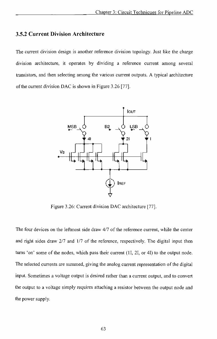
Chapter 3: Circuit Techniques for Pipeline ADC
3.5.2 Current Division Architecture
The current division design is another reference division topology. Just like the charge
division architecture, it operates by dividing a reference current among several
transistors, and then selecting among the various current outputs, A typical architecture
ofthe current division DAC is shown in Figure 3,26 [77],
Figure 3.26: Current division DAC architecture [77].
The four devices on the leftmost side draw 4/7 of the reference current, while the center
and right sides draw 2/7 and 1/7 of the reference, respectively. The digital input then
turns 'on' some ofthe nodes, which pass their current (II, 21, or 41) to the output node.
The selected currents are summed, giving the analog current representation ofthe digital
input. Sometimes a voltage output is desired rather than a current output, and to convert
the output to a voltage simply requires attaching a resistor between the output node and
the power supply.
63

Chapter 3: Cfrcuit Techniques for Pipeline ADC
There are two major disadvantages with current division topologies, Ffrst, the stack of
current dividing transistors positioned above IREF reduces the available output voltage
range, and therefore can be impractical in low voltage circuits. This is precarious,
because if the output voltage decreases enough, the current dividers may go out of
saturation. Secondly, since each device divides the reference current, IREF must be N
(the total number of input levels) times greater than each ofthe output currents. This can
require a huge device to provide the current source.
3.5.3 Resistor-Ladder Architecture
The resistor-ladder architecture is a string of resistors in series, with the 'top' resistor
tied to power and the 'bottom' resistor connected to ground, as shown in Figure 3,27
[78],
, VBEF
IHI (D
^ - ^
VOUT
Figure 3,27: Resistor-Ladder DAC with thermometer decoding [78],
The nodes in between each resistor have different voltages depending on their proximity
to power. Nodes that are higher in the ladder have higher voltages, and by using
64

Chapter 3: Cfrcuit Techniques for Pipeline ADC
thermometer or binary decoding on the digital signal one specific node can be selected
as the correct analog voltage. The number of resistor elements determines the resolution
ofthe resistor-ladder DAC, An M-bit DAC requires a ladder with 2!^ resistors.
Resistor-ladder DACs have some other advantages besides being simple to design. They
are naturally monotonic as long as the switching elements are designed correctly, and
their differential non-linearity (DNL) and integral non-linearity are relatively low
compared to other architectures. Due to these advantages, the resistor-ladder DAC is a
good candidate to be used within the pipeline ADC.
3.6 Proposed Circuit Techniques for most Critical Components in ADC Design
This section describes and analyses the two most critical circuit designs used within the
pipeline ADC architecture, which are the sample-and-hold (S/H) circuit and the
dynamic comparator,
3.6.1 Proposed Sample-and-Hold Circuit
The proposed S/H circuit employed within the pipeline ADC architecture is a
modification to the S/H illusfrated in Figure 3.28 [76], Before analysing the proposed
S/H circuit, illusfrated in Figure 3,29, the S/H circuit of Figure 3,28 must first be
understood.
65

Chapter 3: Circuit Techniques for Pipeline ADC
^ m * ^ " ^ ^
LV
•elk
I [> V^
aV • ^out
Figure 3.28: S/H circuit with an op-amp in a feedback loop [79]
When the clock ^cik is high, the complete circuit responds similarly to an op-amp in a
unity-gain feedback configuration. When ^cik goes low, the input voltage at that time is
stored on C/,, similarly to a simple S/H. By including an op-amp in the feedback loop,
the input impedance of the S/H is greatly increased. Another advantage of this
configuration is that even if the unity-gain buffer at the output has an offset voltage, the
DC error due to this buffer will be divided by the gain ofthe input op-amp, although the
input offset of the input op-amp will remain. Thus, very simple source followers can be
used for the output buffer.
V \ n ^ ^
Clk_Inw K
%
H ^ - ^
I- nf' ^ M
&5
• Vgwt
Figure 3,29: Proposed Sample-and-Hold Circuit
66

Chapter 3: Cfrcuit Techniques for Pipeline ADC
In the design of Figure 3,29, the holding capacitor is not dfrectly coimected to ground,
but it is placed in the feedback loop with another op-amp. Assuming the second op-amp
has a large gain, the input to the second op-amp is basically at zero volts. Therefore, the
voltages on both sides of switch Mo are nearly signal independent. Thus, when Mo turns
'off, there still be charge injection and clock feed-through to the left side of Cf,.
However, it is only going to be a DC offset and will be signal independent and cause no
distortion. In addition, because the voltages on both sides ofthe switch Mo is fixed close
to ground, the finite clock rise time and fall time will not cause any sampling jitter.
Another advantage of this design as compared to the design of Figure 3,28 is due to the
inclusion of Mi. This switch has two main benefits. It grounds the output ofthe first op-
amp during the hold operation. During the sample operation, the voltage at this node has
to go to the inverting input of the second op-amp, which is also close to ground.
Therefore this approach reduces the voltage swing at this node when the S/H goes from
hold operation to sample operation, and hence speeds up the acquisition time. The
switch also minimises the signal feed-through when the S/H is in hold operation by
grounding the signal path. The analysis results of the proposed S/H circuit are shown in
Table 3,1.
Table 3,1: Proposed Sample-and-Hold Results
Property
Sampling Rate SFDR
Signal swing Supply Voltage
Power Consumption Technology
Result
15,36 MSPS 64dBc 1,3 V 2,5 V
0,22 mW 0,18^mCMOS
67

Chapter 3: Cfrcuit Techniques for Pipeline ADC
3.6.2 Proposed Comparator Circuit
This section describes the design of the latch comparator used in the proposed ADC
architecture. In an ADC, comparators are the most critical components that directly
affect the ADC overall performance. Their input offset voltage, delay and input range
directly influence the resolution and speed of the ADCs, Fundamental function of
comparators is to compare an input signal (F,„) with a reference signal (VRej) and then to
generate the high logic value when Vi„>VRef and low logic value when Vi„<VRef. The
proposed comparator consists of a CMOS latch amplifier circuit and an S-R latch circuit
hugging the CMOS latch amplifier, as illustrated in Figure 3.30. The CMOS latch
circuit consists of a differential pair using PMOS switches (Mo, Mi and M2) and a cross-
coupled circuit using NMOS transistors (Mg, Mu). The roles of PMOS switch
transistors (M3 and M4) and NMOS switch transistors (Mio and Mn) are to isolate the
differential pair and the cross-coupled pair and to discharge the drains of M9 and Mu to
ground to keep the output unchanged of S-R latch circuit (Ms Ms, M7, Mg, Mi3_ Mi4_ Mis,
Mis) during the re-charge mode. The comparator operation is described as follows: In
re-charge mode (when the clock signal is high), the differential pair and cross-coupled
circuit are isolated. The drain gates of the NMOS transistors are pulled to ground while
the drain gates of the positive-channel metal oxide semiconductor (PMOS) fransistors
are pulled to VDD- When the clock signal goes low. Mo acts as a current source providing
current ID given by:
Io=^j(K^s-Voo-Vry (3.13)
where k = ^pC^, Vbias is the bias voltage, VT is threshold voltage. Wis the width of that
particular fransistor, and L is the corresponding length ofthe fransistor.
68

Chapter 3: Cfrcuit Techniques for Pipeline ADC
Figure 3,30: Dynamic Comparator Circuit
The voltage difference between F,„ and VRC/, will induce difference currents IDI and ID2
flowing in two perfectly matched PMOS fransistors (Mi and M2). These currents are
represented as follows [80]:
(3.14)
/„,=Z^-:^AF- | 4 ^ - A r D\ 2 AL (W^
(3.15)
where Ar=K/„- r^e /
These different currents create the regeneration process of the NMOS switches Mg and
Mil. The regeneration process could be further explained by the help of Figure 3.31.
69

Chapter 3: Cfrcuit Techniques for Pipeline ADC
^eql IQI ID2 ^eq2
Figure 3.31: Cross coupled pair of comparator
The capacitors C/ through Cj are lumps into Ceqi and Ceq2- This approximation is valid
because grounded capacitance has dominant value and one can represent the much
smaller coupling capacitance due to the Miller effect [81]. The inputs currents initially
charge the input capacitances Ceqi and Ceq2, while switches Mio and Mi2 are tumed off.
The rising of gate voltage of switches Mg and Mu will increase the drain current. The
regenerative action starts when the closed-loop gain through switches Mg and Mu
become greater than one [81]. This gain is given by:
gmg-RL9-S^u-^Ln > 1 (3.16)
where Rig and Rm are the load resistances of fransistor Mg and Mu respectively. This
phenomenon occurs when both Mg and Mu are in deep subthreshold region. The
regenerative action starts when [81]:
70

Chapter 3: Circuit Techniques for Pipeline 7\DC
> (X-4-Vy « 3x10" (3.17)
where parameter A, is a linear function of effective channel length and V, is the threshold
voltage. Suppose that F,„ > VRef then IDI < IDI-, therefore V2 will rise faster than Vi. Due
to the regenerative action, increasing V2 will fiirther decrease Vi. When V2 > Vi+Vrthe
NMOS Mil will go to saturation mode, thus it will pull voltage Vi to ground, where
NMOS Mg will be cut-off, and hence V2 will be pulled up to VDD- Figure 3,32 illustrates
the regeneration process.
Voltage
Initi d Charging 0^ Parasi tic Capacitai^ce
Regeneration Process
y Charging !J*arasitic Capaci{ance
Time
Figure 3.32: Regeneration Process [81].
3.6.2.1 Comparator Optimisation
The proposed comparator offers three main advantages, namely high speed, small
device size and minimal static power dissipation. However, the offset error of this
comparator is typically large. The reason for this is because when Vi„ and VRC/ are
approximately equal to each other, roughly equal input currents to the regeneration
71
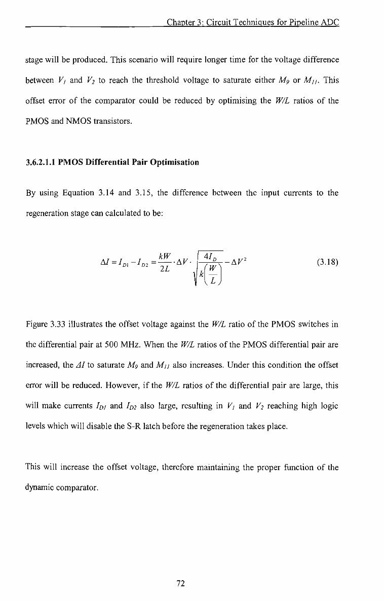
Chapter 3: Cfrcuit Techniques for Pipeline ADC
stage will be produced. This scenario will require longer time for the voltage difference
between Vi and V2 to reach the threshold voltage to saturate either Mg or Mu- This
offset error of the comp^ator could be reduced by optimising the W/L ratios of the
PMOS and NMOS fransistors,
3.6.2.1.1 PMOS Differential Pair Optimisation
By using Equation 3,14 and 3.15, the difference between the input currents to the
regeneration stage can calculated to be:
kW AI ^='m-Jo2=^rr-^f-l-jf^-'^^' (3-18) 2i ., ,
L
Figure 3,33 illustrates the offset voltage against the W/L ratio ofthe PMOS switches in
the differential pair at 500 MHz, When the W/L ratios ofthe PMOS differential pair are
increased, the AI to saturate Mg and Mu also increases. Under this condition the offset
error will be reduced. However, if the W/L ratios of the differential pair are large, this
will make currents IDI and ID2 also large, resulting in Vi and V2 reaching high logic
levels which will disable the S-R latch before the regeneration takes place.
This will increase the offset voltage, therefore maintaining the proper function of the
dynamic comparator.
72

Chapter 3: Circuit Techniques for Pipeline ADC
W/L Ratio
Figure 3,33: Optimisation of PMOS transistor pair
Hence, the offset error initially decreases as the W/L ratios are increased, and then as the
W/L ratios are further increased, the offset error increases. The optimised W/L ratios of
the PMOS fransistors are obtained when the offset error of the comparator is at its
minimum value of ImV, Table 3,2 shows the appropriate W/L ratios of these transistors.
Table 3,2: W/L Ratios ofthe PMOS transistors
Transistors (Figure 3.30)
Mo
Ml M2
W/L Ratio
5.6
2,94 2.94
3.6.2.1.2 NMOS Regeneration Circuit Optimisation
The switching time of a fransistor is given by [80]:
1 V^-WL-C To = — = 2;r
fr lo p (3.19)
73

Chapter 3: Circuit Techniques for Pipeline ADC
where/r is the switching frequency and Cjs is the source junction capacitance. Reducing
the lengths and widths of Mio and Mn will produce smaller switching time, however
this will be greatly influenced by the technology used. For the cross-coupled pafr of the
comparator, the drain current ID of the NMOS fransistor in the subthreshold region is
given by [80]:
W I^=--qXD„-n^, •e^ "'-e nVt ) ^
f 1-l J
(3.19)
where W is the width, L is the length, XD„ is the depletion-layer width, and q is the
charge. By increasing the W/L ratios of the NMOS transistors will produce larger ID and
therefore the regeneration process will begin sooner than as stated by Equation 3.17.
Figure 3.34 illustrated the offset voltage as a function ofthe W/L ratios ofthe NMOS
transistors in the regeneration circuit.
4.5
4
3.5
M10(W/L) = M12(W/L) = 4.71 M10(W/L) = M12(W/L) = 2.35 M10(W/L) = M12(W/L) = 1.17 M10(W/L) = M12(W/L) = 0.24
1 1.5 2 2.5 W/L Ratios Of M9&M11
3.5
Figure 3,34: Optimisation of NMOS regeneration circuit
74

Chapter 3: Cfrcuit Techniques for Pipeline ADC
As the lengths and widths of Mio and M12 are decreased, the comparator offset error
reduces accordingly. While the W/L ratios of Mp and Mu are increased, the offset error
mitially is reduced, and as the W/L ratios are further increased, the offset error is also
increases. Table 3,3 presents the NMOS transistor values for minimum offset error.
Table 3,3: W/L Ratios of Regeneration circuit transistors
Transistors (Figure 3.30)
Mg
Mio Mil
M12
W/L Ratio
1.18 0,24 1.18 0.24
3.6.2.1.3 S-R Latch Optimisation
The most critical optimisation of the comparator circuit is the optimisation of the S-R
latch circuit. It is the S-R latch that holds the output of the comparator when the
comparator is in recharge mode. The information is required to be ready at the output of
the S-R latch before the comparator changes to the recharge process. Thus, the smaller
the delay time ofthe S-R latch, the more accurate the result would be.
The rise time and fall time of the output signals must be balanced, therefore
optimisation of the S-R latch involves minimising the widths and lengths of the NMOS
and PMOS fransistors while maintaining balanced rise and fall time. At ahnost perfectly
balanced rise time and fall time, the W/L ratios ofthe fransistors within the S-R latch are
shown in Table 3,4,
75

Chapter 3: Circuit Techniques for Pipeline ADC
Table 3,4: W/L Ratios of S-R Latch
Transistors (Figure 3.30)
Ms Ms My Ms
W/L Ratio
1,25 1,25 1,25 1,25
3.6.2.2 Comparator Analysis
Optimisation strategies, such as the ones described above will reduced the offset error of
the dynamic comparator at certain sampling frequencies. However, the sampling
frequency has a rather big influence on the offset error. Figure 3.35 illustrates the offset
error ofthe comparator as a function of various sampling frequencies.
6-
> E r 4 2 m % 3 .<f>
0 100 200 300 400 500 600 700 800 900
Frequency (MHz)
Figure 3,35: Comparator Offset Error as function of Frequency
From Figure 3,35, it can be seen that for frequency less then 250 MHz, the offset error
is less than 100 |xV, and only ImV at 500 MHZ. The offset error is fairly linear between
76
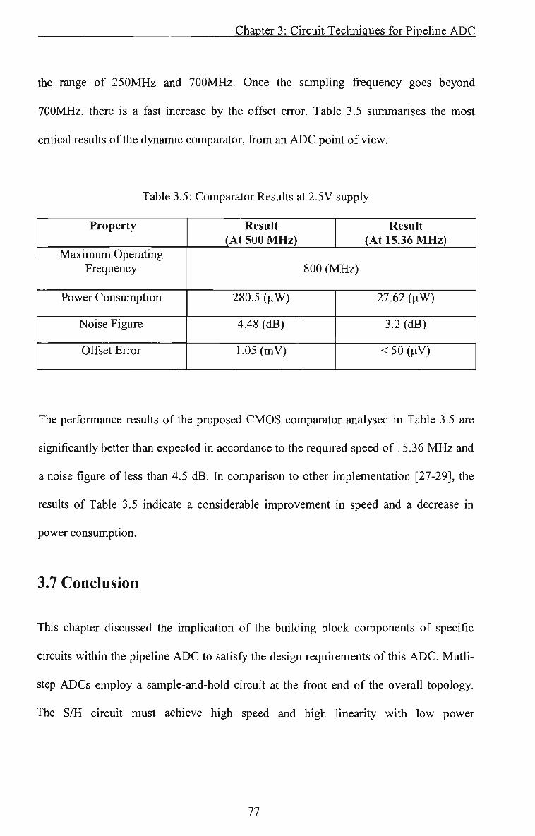
Chapter 3: Circuit Techniques for Pipeline ADC
the range of 250MHz and 700MHz. Once the samphng frequency goes beyond
700MHz, there is a fast increase by the offset error. Table 3,5 summarises the most
critical results ofthe dynamic comparator, from an ADC point of view.
Table 3.5: Comparator Results at 2,5V supply
Property
Maximum Operating Frequency
Power Consumption
Noise Figure
Offset Error
Result (At 500 MHz)
Result (At 15.36 MHz)
800 (MHz)
280,5 ( iW)
4,48 (dB)
1.05 (mV)
27,62 (iiW)
3,2 (dB)
< 50 ( iV)
The performance results ofthe proposed CMOS comparator analysed in Table 3.5 are
significantly better than expected in accordance to the required speed of 15,36 MHz and
a noise figure of less than 4,5 dB, In comparison to other implementation [27-29], the
results of Table 3,5 indicate a considerable improvement in speed and a decrease in
power consumption,
3.7 Conclusion
This chapter discussed the implication of the building block components of specific
circuits within the pipeline ADC to satisfy the design requirements of this ADC. Muth-
step ADCs employ a sample-and-hold circuit at the front end of the overall topology.
The S/H circuit must achieve high speed and high linearity with low power
77

Chapter 3: Cfrcuit Techniques for Pipeline ADC
consumption. Additionally, sampling circuits can be used to improve the timing and
bandwidth boundaries of one-step converters such as flash architectures.
On the other hand, design of fast exactness comparator circuits requires vigilant trade
offs among parameters such as speed, power consumption, and resolution. The
resolution of a comparator circuit is inhibited by the input offset of its latch, while the
speed is often limited by the preamplifier override recovery. From this statement, it can
be summarised that if the latch offset is reduced in a reliable way, the preamplifier can
be designed for lower gain and therefore faster recovery. CMOS comparator techniques
have been introduced, in particular the offset cancellation technique. To achieve a small
residual offset, the technique combines a preamplifier circuit and a regenerative latch,
both with offset cancellation. This architecture radically unwinds the preamplifier gain
requirements, allowing high speed and low power consumption. This chapter also
described design techniques for operational amplifiers, which are utilised for low
power, high-speed, and low-voltage data converters.
78

Chapter 4: Sub-ADC Architecture
Chapter 4
Sub'AD C A rch itecture
4.1 Introduction
The objective of this research is to design and implement a low power, reduced
complexity reconfigurable ADC for a mobile terminal receiver. The resolution of the
ADC will be scaled according to the interference experienced by the adjacent channel
and co-channel interferers. This chapter exploits the findings of chapter 2, where a
pipeline ADC topology, due to its good combination of high speed and low power
consumption, is the most suitable ADC architecture for the mobile receiver. In a
pipeline ADC, the most critical component is the sub-ADC, so careful investigation and
a wise choice of what kind of sub-ADC should be used, is most important. Usually, the
flash topology is employed, due to its fast speed, but because our concern here is power
consumption, we managed to create new design of a modified-flash ADC, In order to
get an in depth knowledge of the performance of an ADC, static and dynamic
specifications for a standard ADC are also defined in this chapter. Prior to designing the
sub-ADC, knowledge on the resolution of the first pipeline block is required, A
79
Chapter 4: Sub-ADC Architecture
statistical analysis on the dynamic range for this design is performed, which in fact
justifies the design of a 4-bit sub-ADC in the first block ofthe pipeline chain,
4.2 ADC Specifications
In order to fully understand the performance of any ADC, the specifications ofthe static
and dynamic domains need to be addressed. Firstly, the static domain, where the
integral non-linearity (INL) and differential non-linearity (DNL) of the converter is
described. Secondly, the dynamic domain where the communications specifications,
such as signal-to-noise ratio (SNR), total harmonic distortion (THD), effective number
of bits (ENOB) and the dynamic range (DR) are described.
4.2.1 Static Specifications
The most considerable evaluation of static specifications of an ADC is the DNL and
INL, The properties of these specifications include the quantisation error or noise {Q„)
of the converter, which is associated with the accuracy of the ADC, By analysing the
transfer curve of an ADC, the integral non-linearity and differential non-linearity could
be defined and explained,
4.2.1.1 ADC Differential Non-Linearity (DNL)
The ADC differential non-linearity can be calculated from the fransition voltages, which
are calculated from the histogram ofthe captured data points, shown in Figure 4,1,
80
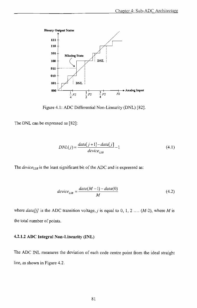
Chapter 4: Sub-ADC Architecture
Binary Output States
» Analog Input
Figure 4,1: ADC Differential Non-Linearity (DNL) [82].
The DNL can be expressed as [82]:
^ ^ data[J + l]-data[J] _
device LSB
(4.1)
The deviceisBi^ the least significant bit ofthe ADC and is expressed as:
device j^gg = data{M-l)-data{0)
M (4,2)
where data/jj is the ADC fransition voltage,y is equal to 0, 1, 2 ,,.. (M-2), where Mis
the total number of points,
4.2.1.2 ADC Integral Non-Linearity (INL)
The ADC INL measures the deviation of each code cenfre point from the ideal straight
line, as shown in Figure 4,2,
81

Chapter 4: Sub-ADC Architecture
Binary Output States 4
\—>• Analog Input
Figure 4,2: ADC fritegral Non-Linearity (INL) [83],
The INL of an ADC can be expressed as follows [83]:
J ^ data[j] - (devicei^sB ' J + ^^^[0])
device^sB (4.3)
where the deviceisB is also equivalent to data{M -l)-data{0)
M
4.2.2 Distortion Characteristics (Dynamic Specifications)
Distortion measurement is obtained by sourcing the input sine wave to the system. The
analog response is first captured and then analysed in the frequency domain. This means
that the processed waveform is converted into its spectrum using the Fast-Fourier-
Transform (FFT) algorithm, and the calculations are based on the frequency
components.
Typical distortion measures are:
• Total Harmonic Distortion (THD)
82

Chapter 4: Sub-ADC Architecture
• Signal-to-Noise Ratio (SNR)
• Signal-to-Noise plus Distortion Ratio (SNDR)
• Spurious Free Dynamic Range (SFDR)
• Effective Number of Bits (ENOB)
4.2.2.1 Total Harmonic Distortion (THD)
The THD compares the combined power of the M harmonics with the power of the
input signal. The THD is described and calculated as the ratio of the root mean square
(rms) sum of the first M harmonic components, usually up to the 5*'' harmonic, to the
rms value ofthe full-scale input voltage signal (VFS)- The THD expressed in decibels
(dB) is [83, 84]:
THD = 20-log
\M \
Ji ; \j=2
F,
\ J
(4,4)
where Fj (j=2 M) are the harmonics of the output signal, M is the number of
harmonics, and Fh is the fundamental ofthe output signal,
4.2.2.2 Signal-to-Noise Ratio (SNR)
The SNR is calculated as the ratio ofthe rms value ofthe input signal to the rms sum of
all other specfral components below the Nyquist frequency, excluding harmonics. The
SNR is expressed as [83, 85]:
83

Chapter 4: Sub-ADC Architectxu-e
SNR = 20-log . f (4,5) Tnaxa».
where Ff is the fundamental of the input signal, Mj are the spectral noise components
excluding harmonics, maxsw and minBw are the maximum and minimum bandwidths,
respectively. Equation 4,5 could also be expressed in terms of dB for a single-tone sine
signal, where SNR is given by [86]:
A /? = 2 ' ' J - = ( 6 , 0 2 M + 1,76) dB (4.6)
Equation 4,6 indicates that each additional bit, M, enhances the SNR by 6.02 dB.
4.2.2.3 Signal-to-Noise plus Distortion Ratio (SNDR)
The SNDR compares the power of the input signal with the combined power of the
harmonics and noise. SNDR is calculated as the ratio of the rms value of the input
signal to the rms sum of all other spectral components below the Nyquist frequency
(Nf), including harmonics. The Nyquist frequency (A ) is defined as:
m- Sampling Frequency ,. „.
The SNDR is expressed as [85]:
F SNDR = 20 • log , ^ (4,8)
84
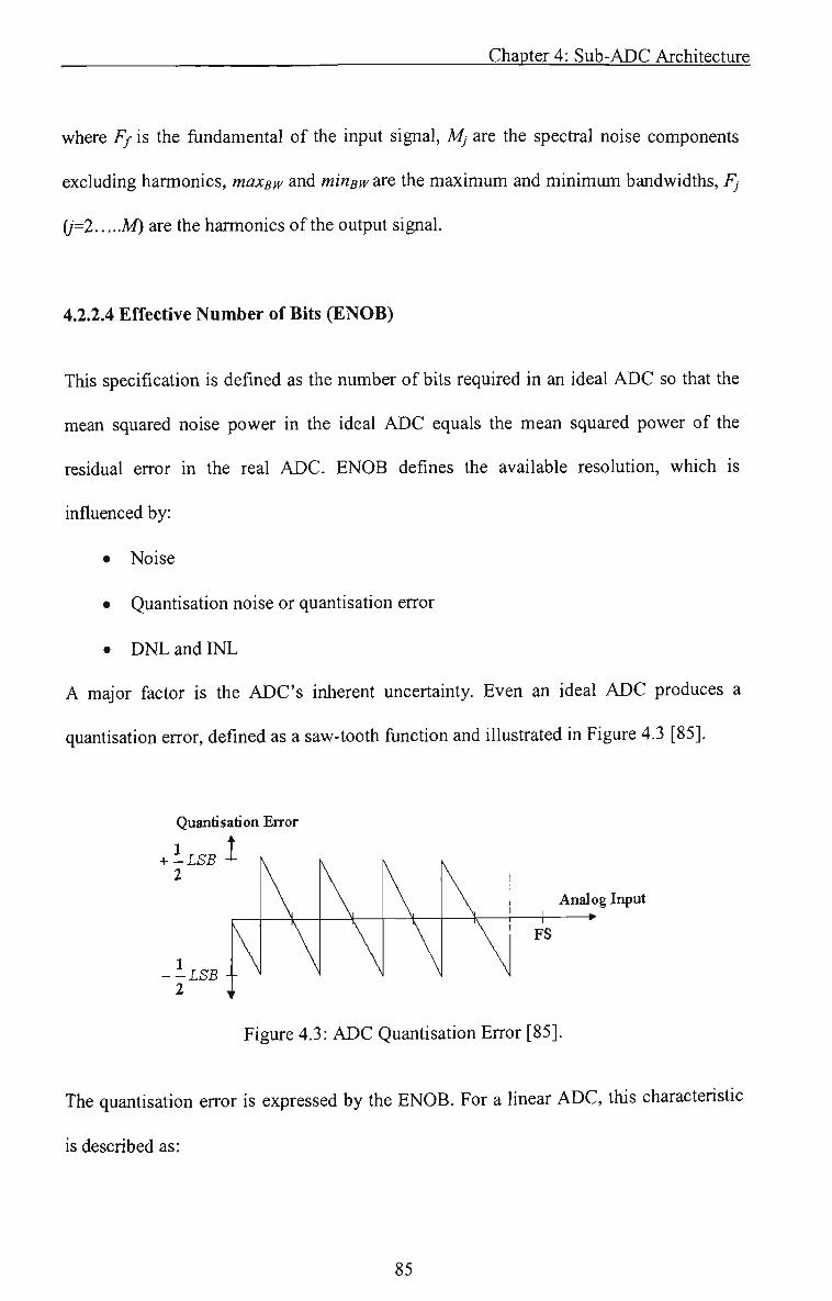
Chapter 4: Sub-ADC Architecture
where Ff is the fundamental of the input signal, Mj are the specfral noise components
excluding harmonics, maxsw and minBw^xe the maximum and minimum bandwidths, Fj
(1=2 M) are the harmonics ofthe output signal,
4.2.2.4 Effective Number of Bits (ENOB)
This specification is defined as the number of bits required in an ideal ADC so that the
mean squared noise power in the ideal ADC equals the mean squared power of the
residual error in the real ADC. ENOB defines the available resolution, which is
influenced by:
• Noise
• Quantisation noise or quantisation error
• DNL and INL
A major factor is the ADC's inherent uncertainty. Even an ideal ADC produces a
quantisation error, defined as a saw-tooth function and illustrated in Figure 4.3 [85],
Quantisation EjTor i
+ -LSB -2
--LSB -2
L
\ _ ^
\ ' A
\ FS
nalo — ^
Figure 4,3: ADC Quantisation Error [85].
The quantisation error is expressed by the ENOB, For a linear ADC, this characteristic
is described as:
85

Chapter 4: Sub-ADC Architectiire
^^^^„ SNR-1.76 ENOB = (4 9)
6,02 ^ ^
4.2.2.5 Spurious Free Dynamic Range (SFDR)
The SFDR is the ratio of the largest spectral component to the rms value of the full-
scale input signal, and is described as [87]:
SFDR = 20-log (v ^
' sc (4.10)
where Vsc is the voltage amplitude ofthe maximum spurious component, and f^is the
voltage amplitude ofthe fundamental,
4.2.3 Receiver ADC Dynamic Range Analysis
The dynamic range (DRADC) of an ADC is the input power for which the signal-to-noise
ratio of the ADC is greater than zero dB, To obtain the dynamic range the SNR as a
function of the input power needs to be calculated. The number of bits can also
determine the DR of an ADC,
This section presents the receiver ADC's dynamic range analysis which justifies the
design of a 4-bit first stage ADC of the entire pipeline chain. Altering the word-length
(bits) of the ADC can have a severe impact on the performance of the receiver if the
word-length is reduced. This may occur if the DR of the ADC may be below a certain
tolerance level, A dynamic range analysis with respect to a variable word-length ADC
86

Chapter 4: Sub-ADC Architecture
must be investigated to determine which word-lengths will not affect the noise
performance of the receiver. The relationship between DRADC and the effective number
of bits N, has been investigated in [87] and is as follows:
DR,^,=20-\og,,{2') (4,11)
Equation 4,10 yields 6,02 dB of dynamic range per bit, therefore is simplified to:
DR^j,r = 6.02-N [dB] (4.12)
To obtain the corresponding effective number of bits if the dynamic range is known, N
corresponds to:
^=^^ADC
6.02 (4.13)
Figure 4.4 illustrates the dynamic range ofthe ADC with variable resolutions.
100
4 6 8 to Wordlength (bits)
12 14 16
Figure 4,4: Dynamic Range Analysis ofADC
87

Chapter 4: Sub-ADC Architecture
The required system signal-to-noise ratio, which needs to be met for adequate
performance, is 6.5dB. An additional safety margin of 2 bits would be acceptable to
combat any input spikes. Therefore, acceptable word lengths are > 4. The minimum
word length is 4,
4.3 First Pipeline ADC Stage
The design ofthe first pipeline block ofthe reconfigurable ADC was largely influenced
by the dynamic analysis of the ADC within the UTRA-TDD system. The dynamic
range of the overall system, according to the UTRA-TDD specifications justified that
the ADC could have any number of pipeline stages, which also determines the number
of bit, as long as the minimum resolution is 4-bits. This was justified by Figure 4.4.
From this analysis, highest degree of emphasis must be given to the sub-ADC of the
pipeline architecture, because it is this block that produces the digital output. Usually a
flash ADC topology is used as a sub-ADC of the pipeline, but as described in the
literature review, chapter 2, this design dissipates a lot of power. Therefore a modified
flash architecture has been implemented and compared in terms of power consumption
with the typical flash ADC and the two-step ADC.
4.3.1 Sub-ADC (Modified Flash) Architecture
When speed is the first priority in the design process of an ADC, flash topology ADC is
considered as first choice, but when we add the complexity of the flash ADC, we are
forced to compromise between performance and complexity. The following steps are
used to design the new 4-bit flash ADC.
88

Chapter 4: Sub-ADC Architecture
(i) Start with 2^'^^ + 2 comparators and label them in ascending order, as shown
in Figure 4,5. The analog input voltage Vi„ is connected to the non-inverting
inputs of all the comparators and the inverting input of the MSB comparator
is set to 8VRef/16,4VRef/16 and 12VRef/16.
(ii) The outputs of these 3 comparators are used to control the switches, which
are connected to the appropriate fractions ofthe reference voltage, VRef.
(iii) The outputs of the comparators (Comp4, Comps, Comp6) are encoded into
appropriate values as shown in Table 4,1,
'ref
15V^16
14V^^16
2VR^16
lVw/16
avjis
4Vw/16-
12V,ur/16
9JJ16.
13W16-
2Vw/16 6Vw/16. lDVw/16
14Vw/15
3y/w/16 NJ1&.
llVw/16 ISVfc lfi
Figure 4,5: Modified-Flash ADC Architecture
89

Chapter 4: Sub-ADC Architecture
Table 4,1: Relationship between comparator outputs and ADC outputs
015 0 0 0 a 0 D 0 0 0 0 a 0
fT 0 2 J
014 0 0 0 0 0 0 0 0 0 0 0 0
T 0 1
In ^
013 0 0 0 0 0 0 0 Q 0 0 0 0
T) 1 1 u
012 0 0 0 D 0 0 0 D 0 0 0 0 1 1 1 1
oil 0 0 0 0 0 0 0 0
fO 0
°i In
O10 0 0 0 0 0 0 0 0 0 0 1
_,1 1
\1 \ ^ \ \
09 0 0 0 D 0 0 0 D OTj
1
08 0 0 0 0 0 0 0 0
07 0 0 0 0
fO ^0
06 0 0 0 0 0 0
°! ^ 1 1 1 1 1
\1 \ \ A ^\ 1 1 1
05 0 0 0 0 0]
J
1
\1
\ \ \
04 0 0 0 0
03 (t 0 0 ,
k
02 0 0 1
( v \ \ \ 1\ 1
01 0)
V
, 1 \1 \ \ \
M
D3 0 0 0 0 0 0 0 0
\
02 0 0 0 D 1 1 1 1 0 0 D 0 1 1 1 1
Di 0 0 1 1 0 0 1 1 0 0 1 1 0 0 1 1
00 0 1 0 1 0 1 0 1 0 1 0 1 0 1 0 1
02=1,01^ = 0 Os = 0,0^=1
©!= 0,04=0
0g=l ,0 |5= l
The main advantage of the modified flash ADC approach is the reduction of
comparators, which is most critical and the most area-consuming component in the flash
ADC design. For N-hit of resolution, the modified ADC architecture requires only
(2 " ^ + 2) comparators, comparing to 2' -l comparators required by the full flash ADC
topology. Also, the modified flash ADC requires a much less complex encoder, than
that of the traditional full flash ADC, The encoder logic expressions for the modified-
flash ADC are described below:
D,=0, _ D,=0,+0,.0,
(4,14)
where O, is the output of comparator /.
90

Chapter 4: Sub-ADC Architecture
It should be observed that intentionally the output ofthe second comparator (Comp2) is
switched instead of switching its input in the modified flash ADC, Although a
comparator will be saved if we switch the input of comp2, the speed ofthe system will
dramatically decrease since the data should be available at the output of compi before
the second comparator (Comp2) can initiate its comparison. Using the ADC architecture
in Figure 4.5, the first three comparators (Compi, Compa and Comps) can perform their
comparison simultaneously, and the delay to the selected output is only that of a 2:1
MUX, which is very small, and hence the system sampling speed will be increased.
Another key characteristic ofthe proposed ADC architecture in Figure 4,5 is that it can
perform the conversion in one clock cycle, similar to the full flash ADC topology. The
traditional full flash ADC and the proposed modified ADC both employ the dynamic
latched-type comparator, described in chapter 3, which includes a SR latch to keep the
comparator output during its recharge-mode. In the traditional fiill flash ADC topology,
described in chapter 2, to maximise the sampling speed, the comparators perform their
comparison simultaneously in the first half clock-cycle, and its logic encoder performs
its function in the other half clock-cycle while the comparators maintains their output
values (in recharge-mode). Thus, the digital data should be ready after one-clock cycle.
hi the modified-flash ADC architecture of Figure 4,5, the first three comparators
(Compi, Comp2 and Compa) complete the comparison, the 2:1 MUX perform the
selection and the appropriate reference voltages propagate through the 4:1 MUX to the
bottom three comparators in the first half clock-cycle. In the other half clock-cycle,
while all the data are maintained since the first three comparators keep thefr values in
91

Chapter 4: Sub-ADC Architecture
recharge-mode, the bottom comparators (Comp4, Comps and Compe) perform the
comparison and the last two bits (Di and Do) will be encoded. Obviously, there will be a
reduction of the sampling frequency of the modified flash ADC comparing with that of
the fiill flash but the sampling frequency reduction is minor,
4.3.1.1 Noise Analysis
The existence of noise in CMOS integrated circuits is basically due to the fact that
electrical charge is not continuous but is carried in discrete amounts to the elecfron
charge, and thus noise is associated with fundamental processes in the integrated-circuit
devices. When working at high frequencies, the noise generated within the device itself
will play an increasingly important role in its overall performance [88], Therefore, a
model that can accurately predict the noise characteristics of the device is crucial for
integrated circuit design.
As it was illustrated in Figure 4,5, the modified-flash ADC contains a resistor ladder,
which consists of 16 resistors, two 2:1 switches, three 4:1 switches and six comparators.
The noise model of each of these components is analysed mathematically and presented
in this section.
4.3.1.1.1 Resistor Ladder Noise Analysis
In a passive resistor, thermal noise is the most dominant source of noise, so here we
only consider this type of noise. This noise source is a fundamental physical
phenomenon and is present in any linear passive resistor. In a conventional resistor RL,
92

Chapter 4: Sub-ADC Architecture
as shown in Figure 4,6, the noise source can be represented by a series voltage generator
as [88]:
iRi
T
Figure 4,6: Noise source in resistor [88],
V\=AkTR,Af (4,14)
where k is the Boltzman's constant, T is the operation temperature, RL is the resistor
value. A/is the small bandwidth at frequency/. This type of noise is due to the random
thermal motion of the electrons and is unaffected by the presence or absence of direct
current, since typical electron drift velocities in a conductor are much less than electron
thermal velocities [88], Using equation 4.14, one resistor in the flash ADC resistor
chain ladder generates a noise power of 1.66x10''^•Af(V'^). Therefore the entire resistor
chain will generate a total noise power of 2.656x10' •Af(V ).
4.3.1.1.2 2:1-MUX Noise Analysis
Before considering the entire 2:1 MUX, noise source in a MOS transistor must first be
considered. The major noise sources in a MOS fransistor are thermal noise and flicker
noise,
^ = ^Af^K — Af (4.15) ^gm f
93
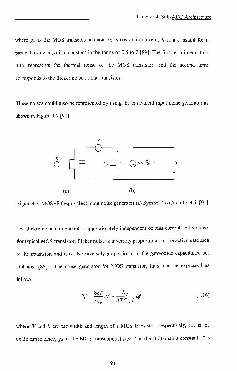
Chapter 4: Sub-ADC Architecture
where gm is the MOS transconductance. ID is the drain current, K is a. constant for a
particular device, a is a constant in the range of 0.5 to 2 [89]. The ffrst term in equation
4.15 represents the thermal noise of the MOS transistor, and the second term
corresponds to the flicker noise of that transistor.
These noises could also be represented by using the equivalent input noise generator as
shown in Figure 4.7 [90].
^ >
O
':t'- ® igaY. < 53
(a) (b)
Figure 4,7: MOSFET equivalent input noise generator (a) Symbol (b) Circuit detail [90]
The flicker noise component is approximately independent of bias current and voltage.
For typical MOS transistor, flicker noise is inversely proportional to the active gate area
of the transistor, and it is also inversely proportional to the gate-oxide capacitance per
unit area [88], The noise generator for MOS transistor, thus, can be expressed as
follows:
V^ = ^Af. 3gm
K,
WLC^J A/ (4,16)
where ^ and L are the width and length of a MOS fransistor, respectively. Cox is the
oxide capacitance, gm is the MOS fransconductance, k is the Boltzman's constant, T is
94
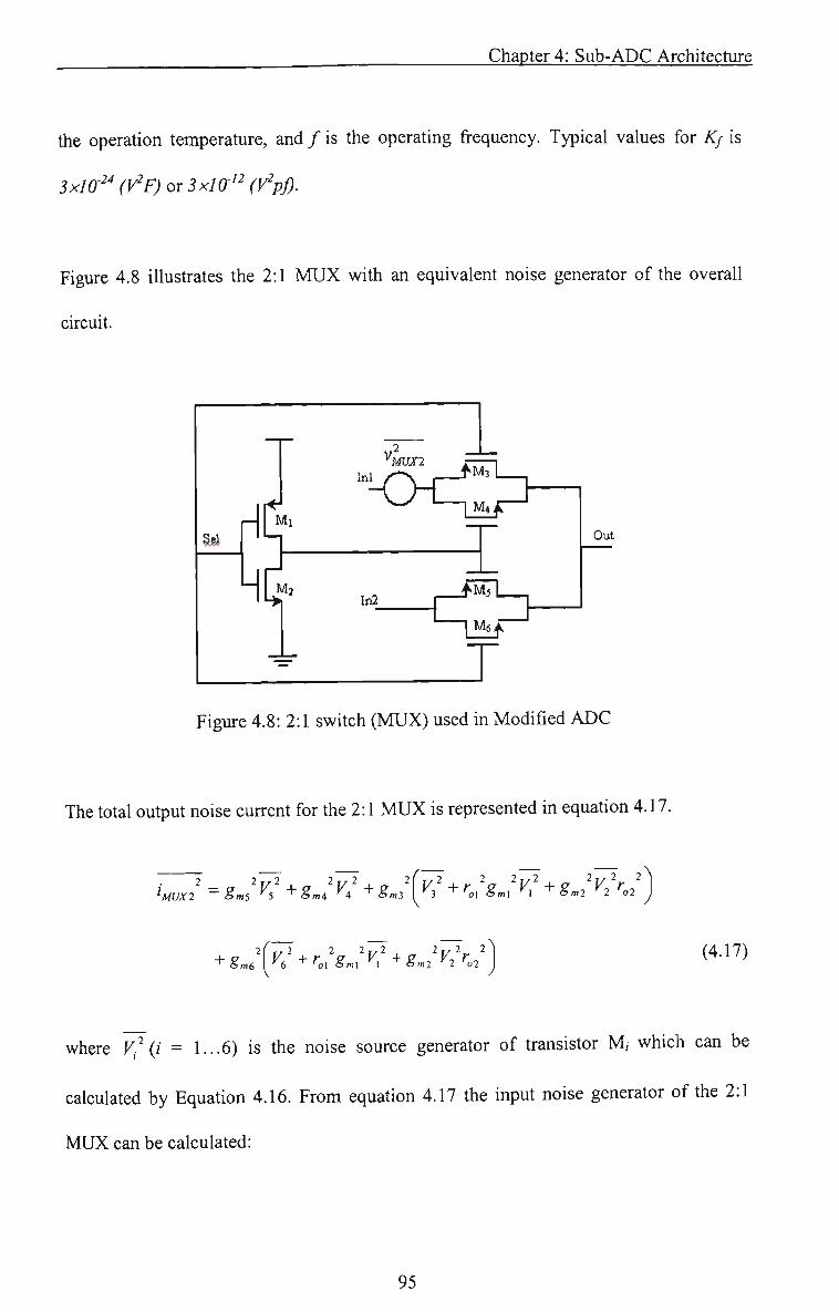
Chapter 4: Sub-ADC Architecture
the operation temperature, and / is the operating frequency. Typical values for Kf is
3x10'^^ (V^F) or 3x10-'^ (V^pf).
Figure 4,8 illustrates the 2:1 MUX with an equivalent noise generator ofthe overall
circuit.
Gilt
Figure 4,8: 2:1 switch (MUX) used in Modified ADC
The total output noise current for the 2:1 MUX is represented in equation 4.17.
i.ux2 = g.x ^8jv:^g„,\v,'^r^:g„:v;^g^x\2) 2{ rr2 2 Ijrl , lr/2 2
+ g«6 [^6 + 01 gm. ^! + g<m Vl 02 (4.17)
where V^ (i = l..,6) is the noise source generator of fransistor M, which can be
calculated by Equation 4.16. From equation 4.17 the input noise generator of the 2:1
MUX can be calculated:
95

Chapter 4: Sub-ADC Architecture
V ' =i Hr IIr y =i '^ MUX2 '•MVX2 yoi"'oAf .
MUX2 r -r
03 04
r + r V'o3 ^ ^ 0 4 7
(4.18)
Using Equation 4,18, one 2:1 MUX generates a total noise power of 4.41x10''^•Af(y^)
at an operating frequency of 400 MHz. Therefore the total noise power generated by the
two 2:1 MUX is 8.82x10-'^•Af(W\
4.3.1.1.3 4:1-Switch Noise Analysis
Figure 4.9 illustrated the 4:1 MUX with the equivalent noise generator included.
Let,
Sell HI M I '^O
HI InvSeli
M ]
Iii2
Sel] ^ InvSi
In3
In4
M i l
M64
J-
M7I
Ms J
Ms I
MM
^M„L
ML
^MBL
| M H ^
Mijl
^MiJL
Ms
Mis>L
Out
|M:
J Figure 4.9: 4:1-MUX used in Modified ADC
y 2 _ 2 2 T ^ 2 2 2 T ^ 2 (4.19)
96
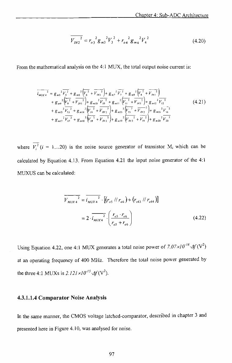
Chapter 4: Sub-ADC Architecture
^^INl' = r^i'Smi'^i' + '"o4'^m4'^4' (4 .20)
From the mathematical analysis on the 4:1 MUX, the total output noise current is:
7 = gj'i^ + gJ^ •^'f^h S„/y,' + g j ^ +Vm')
+ gJ^+Vm^)+g.^o'y7 + g.u'iru^ + ym")+g.nVn' (4.21)
" ^ g / n l ? ' 1 7 ' ' " g m l g \\S "•" ' W2 /"•" g m l 9 \ ' / /V2 "'"''^19 /'^ gm20 ' 2 (
2 16
where V^^ (i = 1,,,20) is the noise source generator of transistor M, which can be
calculated by Equation 4,13, From Equation 4,21 the input noise generator of the 4:1
MUXUS can be calculated:
^MUx/ = IMUX/ • [{^05 II 06 ) + ( 013 / / ^ol4 )]
- 9 • ^ ^o5 ' ^o6
\^o5 "^^06 J
(4,22)
Using Equation 4,22, one 4:1 MUX generates a total noise power of 7.07x10' •Af{V )
at an operating frequency of 400 MHz, Therefore the total noise power generated by
the three 4:1 MUXs is 2.121 xlO''^-Af{W\
4.3.1.1.4 Comparator Noise Analysis
In the same manner, the CMOS voltage latched-comparator, described in chapter 3 and
presented here in Figure 4.10, was analysed for noise.
97

Chapter 4: Sub-ADC Architecture
ri
Vin
Vb Hi
TMI ^ ^ Vref
- ^ ' krH
C 'M5
M7"
Figure 4,10: Dynamic comparator circuit
The input noise generator for one comparator can be described as:
V = comp \gm2 J
vl+2vl+2 f \
\Sm2j vl+2
\gm2 J
• - ( ^ \
vi+2 gmi
\gm2 J
+ 4 g, wlO
. gmlO "*" gml4 v,;+4 6/«
V^mlO "*~§ml4.
(4,23)
Using equation 4,23 one comparator generates a total noise power of 5.3x10' •Af{V )
at an operating frequency of 400 MHz. Therefore the total noise power generated by six
comparators working full time will be 3.18x10'^^•Af(Y^). Detailed noise analysis and
calculations on the latched-comparator used in this design could be found in Appendix
B,
98
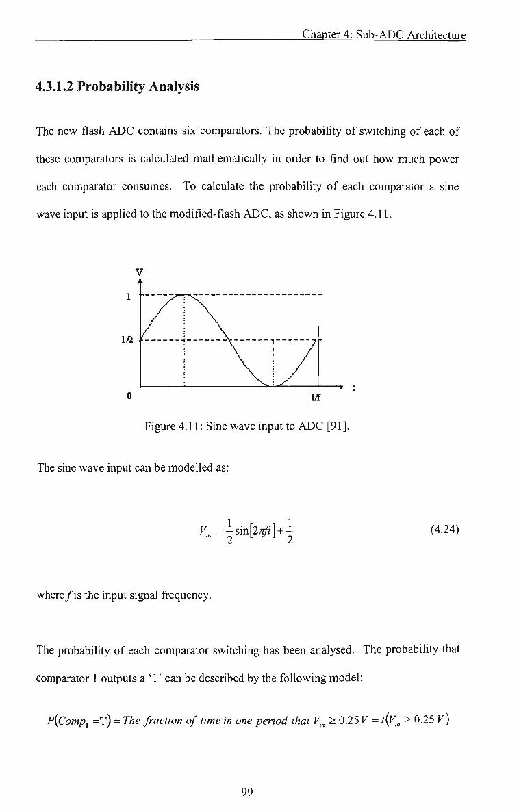
Chapter 4: Sub-ADC Architecture
4.3.1.2 Probability Analysis
The new flash ADC contains six comparators. The probability of switching of each of
these comparators is calculated mathematically in order to fmd out how much power
each comparator consumes. To calculate the probability of each comparator a sine
wave input is applied to the modified-flash ADC, as shown in Figure 4.11,
Ifl •
* t
Figure 4,11: Sine wave input to ADC [91].
The sine wave input can be modelled as:
P^,=isin[2#]+1 (4.24)
where/is the input signal frequency.
The probability of each comparator switching has been analysed. The probability that
comparator 1 outputs a ' 1' can be described by the following model:
P[Comp, ='!') = The fraction of time in one period that F„ > 0,25 V = t{y.„ > 0,25 V)
99

Chapter 4: Sub-ADC Architecture
In similar manner the probability of the rest of the comparators switching were
calculated and are shown below,
P(Comp2 ='l')= t [Vi„ > 0,5 V] (4.25)
P(Comp3 ='!')= t[Vin > 0,75 V] (4.26)
P(Comp4 ='l')= t[Vi„ > 0,8125 V] + f/"0,5625 < Vi„ < 0.15]
+ t [03125 < Vin < 0.57+^/0.0625 < Vm < 0.257 (4.27)
P(Comps ='l')= tfVin > 0.875 V] + //0.625 < Vi„ < 0.15]
+ t [0.315 < Vin < 0.57 +?/"0,125 ^ Vm < 0,257 (4,28)
P(Comp6 ='\')= t[Vin > 0.9315 V] + t [0.6S15 < Vi„ < 0.15]
+ t[0.A315 < Vin < 0.5] +1 [0.1S15 < Vi„ < 0.257 (4.29)
The probability of a certain comparator is off can be described as:
P(Compi ='0') = 1- P(Compi = '\') (4.30)
where / is the comparator number (/ = 1.. .6). Table 4.2 shows the probability switching
of all six comparators, P(Output = '\') describes the probability that a certain
comparator output is on, and P(Output = '0') describes that a comparator output is zero.
The probability of a certain comparator being on or off will affect the noise that the new
flash ADC will generate.
100

Chapter 4: Sub-ADC Architecture
Table 4.2: Probability of each comparator
Comparator number
Compi
Comp2 Comp3 Comp4
Comps
Compe
PfOuput = '1')
0.75
0.5 0.25
0.707
0.5 0.293
P(Output = ' c ;
0.25 0.5 0.75
0.293
0.5 0.707
From the probability analysis of each comparator, it can be stated that the six
comparators are equivalent to three ofthe comparators working full time. Therefore the
total noise power generated can be said to be:
Noise Power = ^•^^''^^—'M. (y\ or 1.59x10''^-Af (V^).
Table 4.3 presents a summary of the noise analysis for each component within the new
flash ADC architecture. The total noise power is also calculated and presented in Table
4.3.
Table 4,3: Summary of noise power in New ADC.
Resistor
2:1 MUX
4:1 MUX
Comp.
Total Noise ofADC
Noise in one component
1.66x10'''-Af
4.41xlO"-Af
7.07xlO'"^-Af
5.30x}0-'^-Af
Number of components in new flash ADC
16
2
3
3 (operating full
time)
Total Noise in specific
components
2.65xlO-"-Af
8.82xlO"-Af
2.12x10'^-Af
1.59xia"-Af
4.86x10'^-Af
101
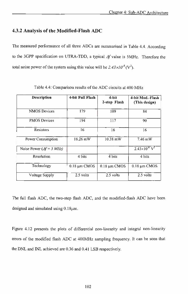
Chapter 4: Sub-ADC Architecture
4.3.2 Analysis ofthe JVIodified-Flash ADC
The measured performance of all three ADCs are summarised in Table 4,4. Accordmg
to the 3GPP specification on UTRA-TDD, a typical Af value is 5MHz. Therefore the
total noise power ofthe system using this value will be 2.43x10'^ (V^).
Table 4,4: Comparison results ofthe ADC circuits at 400 MHz
Description
NMOS Devices
PMOS Devices
Resistors
Power Consumption
Noise Power {Af= 5 MHz)
Resolution
Technology
Voltage Supply
4-bit Full Flash
179
194
16
18.26 mW
4 bits
0.18 im CMOS
2.5 volts
4-bit 2-$tep Flash
109
117
16
10.38 mW
4 bits
0.18 ^m CMOS
2.5 volts
4-bit Mod.-Flash (This design)
84
90
16
7.46 mW
2.43x10"* V^
4 bits
0.18 im CMOS
2.5 volts
The full flash ADC, the two-step flash ADC, and the modified-flash ADC have been
designed and simulated using 0.18fim.
Figure 4.12 presents the plots of differential non-linearity and integral non-linearity
errors of the modified flash ADC at 400MHz sampling frequency. It can be seen that
the DNL and INL achieved are 0.36 and 0.41 LSB respectively.
102
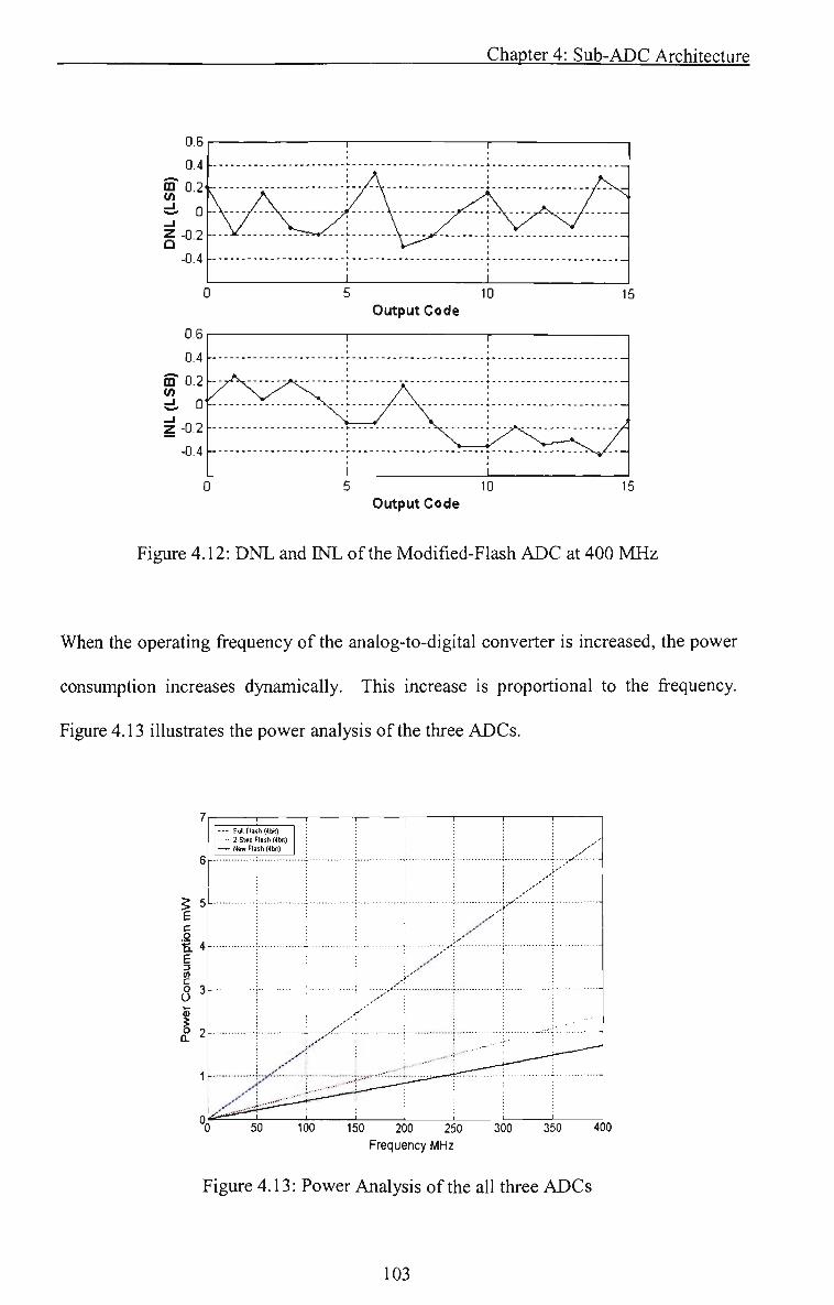
Chapter 4: Sub-ADC Architecture
0.6
0.4
S" 0.2
=i 0
Z -0.2 Q
-0.4
0,6
0.4
m 0.2 v> d. Of
^ -0 .2
-0.4
L - - _ - - - . _ - - . _ _ « _ . _ . . _ . . _ A - - _ . . _ - - - _ . . . _ _ _ . _ _ . _ _ _
5 10 Output Code
5 10 Output Code
15
15
Figure 4.12: DNL and INL ofthe Modified-Flash ADC at 400 MHz
When the operating frequency of the analog-to-digital converter is increased, the power
consumption increases dynamically. This increase is proportional to the frequency.
Figure 4,13 illustrates the power analysis ofthe three ADCs,
1 4
E 3 (A C
2-
1 -
1
— Foil f l » * (<«) 2.Step Flash (4bJ)
— Nsw Flash (4bil)
^
r 1 1 1 1 1
; ; ; ; : ; ^ '
i i i : : ,.-!•''
' i : : .''': 1 : , ' ' 1
i ; ^ / ;
i i i y''' i i i
y
:,,-'' 1 j 1 I--" : ^_^__
i _ (• ' i _ . _ . — — T " " ^ ^
-•(• _ _ „ — r — " " " " ^ ;
i i ; 1 i i
50 100 150 200 250 300 350 400
Frequency MHz
Figure 4,13: Power Analysis ofthe all three ADCs
103

Chapter 4: Sub-ADC Architecture
As mentioned earlier, the comparator is the most critical and the most area-consuming
component of the modified-flash ADC design. Table 4,5 shows the number of
comparators required for all three flash ADC circuits.
Table 4,5: Number of Comparators required for each Flash design
Resolution (bits)
4 6 8 10 12 14 16
4-bit, Full Flash
(2'' - 1 )
15 63
255 1023 4095 16383 65535
4-bit, 2-Step Flash
2(N-1)
8 32 128 512
2048 8192
32768
4-bit Flash (This design)
2(N-2)^2
6 18 66 258 1026 4098 16386
The specifications of the UTRA-TDD system require a sampling rate of only 15,36
MSPS, therefore analysis on the modified-flash ADC has also been performed at this
frequency. Table 4,6 compares the power consumption of all three designs at 15,36
MSPS.
Table 4,6: Comparison results ofthe ADC circuits at 15,36 MSPS
Power Consumption
Supply Voltage
Technology
4-bit, Full Flash
(2^ - 1 )
6.50 mW
2.5 V
0.18 urn CMOS
4-bit, 2-Step Flash 2(N-1)
2.39 mW
2.5 V
0.18 im CMOS
4-bit Flash (This design)
2(N-2)^2
1.68 mW
2.5 V
0.18 im CMOS
From the above analysis, it can be concluded that the advantages of the new ADC
architecture include less components therefore smaller size, and lower power
104
Chapter 4: Sub-ADC Architecture
consumption. These characteristics make this new device better candidate for many
appUcations where power and size are the major factors.
4.4 Conclusion
The Sub-ADC is the most critical component of the pipeline ADC architecture. Making
the right choice of which topology to employ is highly dependent on the design
application. In this research, power consumption is the greatest concem due to the
UTRA-TDD application. The standard flash design can operate at high frequencies, but
it consumes large power due to the high device count. Therefore modification to the
standard flash design has been done to compromise between power consumption and
speed requirement.
The first block of the pipeline ADC, which is a 4-bit, CMOS modified ADC has been
presented in this chapter. It requires only (2 ' ^ + 2) comparators to implement the
modified N-bit flash ADC, This approach greatly reduces the complexity of the full
flash ADC and the two-step flash ADC, The new ADC architectiu-e dissipates only
1.68 milliwatts of power at 15,36 MSPS as compared to a full flash ADC of 6.5
milliwatts and a two-step flash of 2,39 milliwatts. Results indicate that a 74% power
saving is obtained and 53% of die size could be saved when the modified-flash ADC is
used instead of the full flash architecture within the first pipeline ADC block. For
comparison reasons all three analog-to-digital converters were operated at the UTRA-
TDD system-sampling rate of 15,36 MSPS.
105
Chapter 5: Reconfigurable ADC with Fixed Filter
Chapter 5
Reconfigurable ADC with Fixed Filter
5.1 Introduction
In this chapter, a reconfigurable pipeline ADC architecture for TDD mode of the
Universal Mobile Telephone Service, terrestrial radio access is presented. The advances
in this chapter develop the findings of chapter 2, where the sfrength of quantisation
noise (Qn) is dependant on various dynamics and there is a minor probability of highly
severe Qn- Therefore, a fixed length for the receiver ADC would be inefficient resulting
in unnecessary battery power drain. The basic concept of the reconfigurable ADC is to
only utilise the required Qn to meet the specified bit energy to interference ratio
(Eb/No), while restricting the filter adjacent channel protection (ACP) factor within the
receiver at a fixed value of 33 dB, as per the 3GPP specifications.
This is obtained by employing a variable Qn, which yields optimum efficiency. The Q„
power, which meets the required Eb/No depends on the sfrength of ACI powers (out-of-
band) received and the power of the in-band (desired signal and infra-cell interference)
received power. This concept is demonstrated in a spectrum presented in Figure 5,1, As
106

Chapter 5: Reconfigurable ADC with Fixed Filter
illusfrated in Figure 5,1 (a), when the adjacent channel interference (ACI) and the co-
channel interference are both low, the noise floor ofthe ADC can be increased resulting
in low resolution. On the other hand, as shown in Figure 5,1 (b), if the ACI and the co-
channel interference are both high, the noise floor is decreased, providing high
resolution. In the case where the SNR levels are always high, there is a distinct
advantage ofthe proposed pipehne ADC, This means that the ACI will be low, resulting
in low resolution and therefore saving vast amount of power. The in-band and out-of-
band signal powers are monitored in real time.
Low # of ADC Co-channel Interferers
Low ACI High # of Co-channel Interferers ^^
Increase noise Q„
-lOMHz -5MHz I n - B a n d +5MH2 +10MHZ
Out-of-Bands Out-of-Bands
1 Decrease noise Q„ ! -lOMHz -5MH2 I n - B a n d +5MHz +10MH2
Out-of-Bands Out-of-Bands
(a) (b)
Figure 5,1: Spectrum analysis of operational concept of reconfigurable ADC
The chapter is structured as follows: section 5,2 presents and details the reconfigurable
ADC design. All components within the reconfigurable architecture are described
together with their operation, A statistical analysis of the reconfigurable ADC in a
simulation environment is performed in section 5,3, The analysis demonsfrates the
efficiency of the design when applied to the UTRA-TDD system. The statistical
analysis is of a static nature. Section 5.4 describes the implementation of the
reconfigurable ADC, and illusfrates the implemented design. Conclusions are presented
in section 5.5,
107

Chapter 5: Reconfigurable ADC with Fixed Filter
5.2 Reconfigurable Pipeline ADC Design
The architecture of the reconfigurable pipeline ADC consists of a number of
components to enable a scalable Q„. Firstly, the algorithm enabling the ADC to exploit
scalable Qn is formulated and the corresponding system architecture is introduced. The
subsequent sections describe the operation of each of the components in the
reconfigurable architecture.
5.2.1 Algorithm Formulation
In UTRA-TDD, uplink and downlink transmissions are carried over the same radio
frequency by using synchronised time intervals. Time slots in the physical channel are
divided into transmission and reception part. Information on upHnk and downlink are
transmitted reciprocally [89], This makes TDD mode susceptible to ACI as nearby MSs
and BSs cause interference to each other depending on frame synchronisation and
channel asymmetry. This design presents results for downlink UTRA-TDD operation
due to its near far problem. Figure 5,2 [93] presents a multi-operator downlink ACI
scenario in UTRA-TDD,
< » Desired Link Interference Link
,pperator B
Operator A »•"
Figure 5,2: Downlink ACI scenario in UTRA-TDD [90],
108

Chapter 5: Reconfigurable ADC with Fixed Filter
Two interference sources exist in the downlink: adjacent MS and adjacent BS. The
interference overlaps are BS->MS and MS-^MS. If adjacent operators have
synchronised frames and employ the same asymmetry, it would eliminate MS->MS
interference. This cannot be assumed in practice and hence interference is experienced
from both sources dependant on frame synchronisation and asymmetry. To obtain an
understanding, consider Figure 5.3 [93]. User MSi employs a time offset (toff) and both
users MSi and MS2 have time slots (tsiot) that represents the time allocated for uplink and
downlink. Due to the offset in time, each user jams the other in uplink and downlink
mode.
Figure 5,3: UTRA-TDD friterference Overiaps [93].
A synchronisation factor (a) needs to be employed in determining the amount of
interference experienced at a source. This is modeled by the arbitrary time offset, toff
and normahsed by the time slot, tsiot producing [93]:
a = — ^ t slot
(5.1)
109

Chapter 5: Reconfigurable ADC with Fixed Filter
Figure 5,4, illusfrates the architecture of an UTRA-TDD MS receiver [57]. The block
diagram demonsfrates the general operation of the receiver showing the location of the
proposed reconfigurable device in the topology, A control unit is proposed that makes a
comparison between in-band (reference) and out-of-band (comparison) powers and
scales the resolution ofthe ADC,
Outof-Band
In-Band r Ui RF
/
RF — • ADC " : := - -*ylRRC -» H —
i De-
scramble
OSVF„
De-spread
- • De-mod data.
Figure 5,4: UTRA-TDD receiver architecture for one time slot [57],
The algorithm for the reconfigurable ADC is formulated from the Eb/No model given in
Equation 5,2, Considering intra-cell interference is always present as orthogonality may
not be achievable in practice and the received signal powers have been propagated.
EblNo = ^rx'pg
ACT' ?rx' {M-\) + ^^^ + ri + Qn'
(5.2)
where Prx is the received desired signal power at the f" MS in the COI and is defined as
follows:
P ' p I _ ^ rec rx
K (5,3)
110

Chapter 5: Reconfigurable ADC with Fixed Filter
Prx' is determined by the code power of the BS divided by the path loss of the /''' MS
within one time slot in the COI, The processing gain pg and thermal noise rj are known
(static), as well as the target bit energy to interference ratio (Eb/No). Solving Equation
5,2 for Q ; yields:
Pg \
EbINo)
ACT Q;, =Yxx'\\^—^ -^xx'M-^^^—ri (5.4)
ACP
To differentiate the signals the following definitions are needed:
• In-band signal (Prx'M) - This is purely the output of the filter containing the
desired signal as well as intra-cell interference from other MS's served by the
BS within the same timeslot.
• Out-of-band signal (ACI') - This signal is the interference that the receiver RRC
filter has moderated. It can be obtained by using a high pass filter (HPF)
corresponding to an inverse of the receiver filter. This method is inefficient, as
the processing complexity will be doubled. In digital signal processing (DSP), a
HPF equivalent filter can be a subfraction operation where the output ofthe LPF
is subtracted from a delay unit. This is efficient to implement in hardware and is
significantly less costly than a complex HPF,
• Desired signal (Prx^) - This signal can only be obtained once the in-band signal
is de-spread with the corresponding user orthogonal variable spreading factor
(OSVF) code.
111

Chapter 5: Reconfigurable ADC with Fixed Filter
Based on the above definitions, the reconfigurable ADC will be established by a feed
back structure as some receiver processing is requfred to obtain the necessary signals for
a Qn calculation,
5.2.2 Receiver Architecture with Reconfigurable ADC
The reconfigurable ADC architecture for a receiver is proposed in Figure 5,5. The
architecture consists of pipeline ADC architecture, RRC filter, de-spreader, de-
scrambler, de-modulator, decimation factor and signal power measurement. The three
inputs required by the control unit in order to reconfigure the ADC, are obtained from
the filter and the de-spreader. Cleariy varying amplitudes of each signal is required
before they are reprocessed by the control unit where the most efficient Q„ is calculated.
This is achieved by the signal power measurement components in the architecture where
the signals are averaged over a certain length of time.
RFSigr^l- Filter
SC JZ u
i_ De-
scramble
OSVF
L_ De-
spread
fie — 3 g cn Cl Oi
Control Unit
In-Band Power
c
TO w C (D
Cos
O)
&
Out-of-Band Power
De-tnod
daia
(TiS
Desired Signal Power
Figure 5,5: Reconfigurable receiver ADC architectural block diagram
112
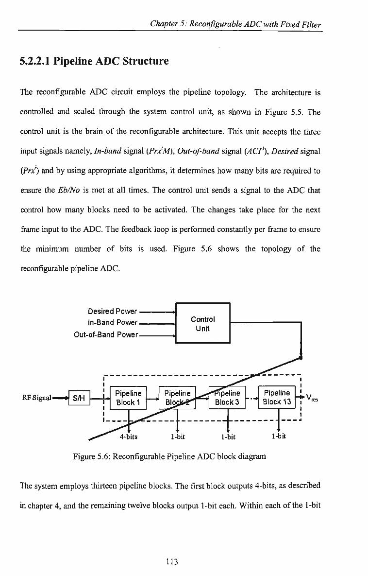
Chapter 5: Reconfigurable ADC with Fixed Filter
5.2.2.1 Pipeline ADC Structure
The reconfigurable ADC circuit employs the pipeline topology. The architecture is
controlled and scaled through the system control unit, as shown in Figure 5,5. The
confrol unit is the brain of the reconfigurable architecture. This unit accepts the three
input signals namely, In-band signal (Prx'M), Out-of-band signal (ACI'), Desired signal
(Prx') and by using appropriate algorithms, it determines how many bits are required to
ensure the Eb/No is met at all times. The control unit sends a signal to the ADC that
control how many blocks need to be activated. The changes take place for the next
frame input to the ADC, The feedback loop is performed constantly per frame to ensure
the minimum number of bits is used. Figure 5,6 shows the topology of the
reconfigurable pipeline ADC.
Desired Power In-Band Power
Out-of-Band Power
Control Unit
^
RF Signal 'res
Figure 5.6: Reconfigurable Pipeline ADC block diagram
The system employs thirteen pipeline blocks. The first block outputs 4-bits, as described
in chapter 4, and the remaining twelve blocks output 1-bit each. Within each ofthe 1-bit
113

Chapter 5: Reconfigurable ADC with Fixed Filter
blocks, a 1.5-bit pipeline topology is used, consisting of a sub-ADC, sub-DAC, and a
gain amplifier,
5.2.2.2 Decimation Factor
The task of the decimation factor in the architecture is simply to down sample the
received symbols by the same factor that is employed in the interpolation stage within
the transmitter. Figure 5.7 illustrates an example of operation of the decimation
algorithm. The decimation factor for 3GPP specification is 4 for the receiver ADC,
therefore down sampling the data rate to 3,84 MHz, The decimation procedure is an
essential process in multirate signal processing. It competently allows the sampling
frequency of the system to decrease without unnecessary effects on the signal such as
the quantisation noise.
Q> T 3 3
.±^ O .
M.
.
a> T 3
3 a. E <
(^
1
1
• •
^ « 1
1 1
» 1 1
* • c B
4 1
<3 »
<
/ S a m p l e s 15.36 MHz , - ' "
J r' <»" > 1 ^
1
J These are the output samples
1
Samples 3.84 MHz
Figure 5,7: Decimation operation, down sampling by factor of 4,
114

Chapter 5: Reconfigurable ADC with Fixed Filter
In the TDD receiver mode, the decimation phase only allows every fourth sample of its
input to go through to the output, therefore omitting every three samples of its input,
5.2.2.3 Signal Power Measurement
The signal power measurement consists of two components, which are the fiill wave
rectifier (FWR) and the averaging filter (AF), Figure 5,8 illusfrates the operation ofthe
signal power measurement component.
Signal Power Measurement
L FWR
*—
Averaging Filter
/ ' i r\ A /•} )
Figure 5,8: Signal Power Measurement
5.2.2.3.1 Full Wave Rectifier
The first component is the FWR. The absolute amplitude of each signal must be taken
before an average is found with the subsequent averaging filter. In digital signal
processing it is a low complex operation. The inverse of each sample is found
dependent if the sample is negative in magnitude. In hardware, the FWR is a two's
compliment operation. Figure 5.9 depicts an example demonstrating the operational
steps for a negative input with a word length of five bits. The first bit is the sign bit and
the subsequent four bits are the magnitude. Figure 5,10 illustrates the operation ofthe
FWR in a flowchart format.
115

Chapter 5: Reconfigurable ADC with Fixed Filter
In =\^J^^
Sign Bit Magnitude
Out = 5 Y= 0 0100 J
+1
Inverse the input, then
add1
0 0101
Out = Y
Figure 5,9: Two's compliment operation in digital hardware with a word
Figure 5.10: Operation ofthe FWR
5.2.2.3.2 Averaging Filter
The averaging filter is a first order HR digital low pass filter (LPF). It computes an
average on a vector of sampled data using a delayed input sample and the previous
output sample for each input sample. The requirement for implementation will not be
costly as only two multipUers and two addition units are required, A delay unit is
represented by Z"^ as shown in Figure 5,11, and the difference equation >>(«> is defined
as follows [94, 95]:
116
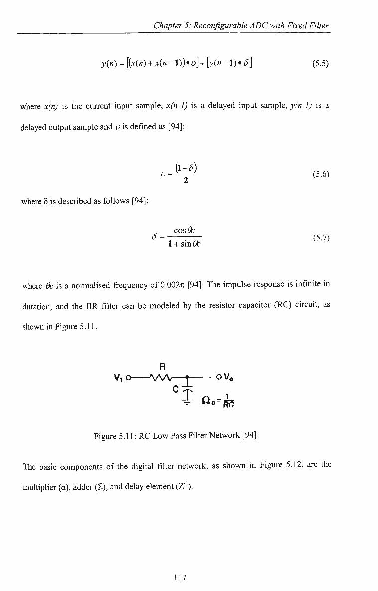
Chapter 5: Reconfigurable ADC with Fixed Filter
y(n) = [(x(«) + x{n - !))• u]+ [y(« -l)»S] (5,5)
where x(n) is the current input sample, x(n-l) is a delayed input sample, y(n-I) is a
delayed output sample and v is defined as [94]:
- ^ (5.6)
where 8 is described as follows [94]:
cos^
where 6b is a normalised frequency of 0.0027t [94], The impulse response is infinite in
duration, and the HR filter can be modeled by the resistor capacitor (RC) circuit, as
shown in Figure 5.11.
R Vi o ^ A A - - f - o Vo
4r Qo=|Jg
Figure 5,11: RC Low Pass Filter Network [94],
The basic components of the digital filter network, as shown in Figure 5,12, are the
multiplier (a), adder (S), and delay element (Z' ),
117

Chapter 5: Reconfigurable ADC with Fixed Filter
x(n)0—T—r>-^ / 1—1=> y<n)
Figure 5.12: Digital Low-Pass Filter Network [94],
The final output sample ofthe filtered data is the average amplitude ofthe entfre stream
of input samples, which is fed to the control unit.
5.2.2.4 Control Unit
The confrol unit is the intelligence in the reconfigurable architecture. It calculates the
required quantisation noise based on the three signals powers, as presented in section
5.2.1, and by using an intelhgent algorithm calculates the appropriate dynamic range of
the ADC, A look-up-table (LUT) is used to intelligently switch the pipeline blocks of
the ADC 'off, if not required, saving significant power.
The Qn is not the only aspect to determine the new length of the ADC. If it was, there
would be a likelihood of some data loss. As the architecture employs a feedback loop,
and two ofthe inputs to the confrol unit come from the filter, the filter length is applied
to the next lot of samples, not the current, therefore any loss of information must be
dealt by the filter.
The architecture reconfigures the ADC to the new length and applies it to the next lot of
samples. As it is a TDD system where a near far problem exists, an adjacent MS may
switch-on close to the MS of interest at the same time it is receiving the next lot of
118

Chapter 5: Reconfigurable ADC with Fixed Filter
samples. If this adjacent MS is transmitting to its base station, it will result in a major
jamming of the signal. Therefore, the minimum 4-bits of resolution may not be
sufficient to meet the system Eb/No. The operation and reconfigurability aspect of the
ADC here is based on a fixed ACP value of 33 dB, obtained from the 3GPP
specifications. In order to obtain the word length of the ADC, the calculated Qn is
substituted in the following equation:
101 log 1 of ^^^' " ' "^ * i)ec//na//o«^ ^
«' = ^ ^ ^ '- + Safety, (5,8)
where n* is the word length of the ADC at a given location in the COI that satisfies the
Eb/No, ACT is the adjacent channel interference ofthe system fixed at 33 dB according
to the specifications ofthe 3GPP, SafetyM is the safety margin of additional 2 dB to take
care of large peaks. Once the Qn of the ADC is calculated from Equation 5,4, the
corresponding resolution can be derived by calculating the dynamic range. The dynamic
range (DR) ofthe ADC is a measure ofthe noise floor in comparison to the largest input
voltage, but in this case, it is in comparison to the largest input wattage yielding:
DR = \0\og f Max "*
10 w
Noise^ J \_dB\ (5,9)
where Noisew is the noise floor assigned to the quantisation noise derived in Equation
5,4, and Maxw is the maximum input wattage defined as a sum of the desired and out-
of-band signal powers and is given by:
119

Chapter 5: Reconfigurable ADC with Fixed Filter
Max^ = [Pj + I^jj j- Decimationf (5.10)
The summation of the desired and out-of-band signal powers are scaled by the
decimation factor, Decimationp. The corresponding ADC resolution is:
n ADC DR 6.02
(5.11)
A LUT can be used to convert the calculated dynamic range from Equation 5,9 to the
corresponding switches to control the pipeline ADC resolution. Equation 5.11 can be
used but will be inefficient as extra computational processing is needed. It will not only
give integer value for the required ADC resolution but floating point values as well.
Hence, LUT is still required to round the calculated resolution to an integer. The LUT to
convert dynamic range to corresponding ADC switches is presented in Table 5.1.
Table 5.1: Control Unit Look Up Table
Dynamic Range (dB)
DR< 24,0804 24,0804 <DR< 30.1005 30,1005<DR<36,1206 36,1206<DR<42,1407 42,1407<DR<48,1608 48.1608 <DR< 54.1809 54.1809<DR<60,2010 60,2010<DR< 66,2211 66,2211 <DR< 72.2412 72.2412 <DR< 78,2613 78,2613 <DR< 84,2814 84.2814<DR< 90,3015 90.3015 <DR< 96,3216
ADC Resolution
4 5 6 7 8 9 10 11 12 13 14 15 16
Bits_Switch (Logic "0" or "1") Corresponding to 13 Pipeline Blocks
1000000000000 1100000000000 1110000000000 1111000000000 1111100000000 1111110000000 1111111000000 1111111100000 1111111110000 11 111 11111000 m i l 111 11100 1111111111110 1111111111111
120

Chapter 5: Reconfigurable ADC with Fixed Filter
The dynamic range is given in dB units but in implementation can be left in units of
watts for simplification, therefore disregarding the log fiinctionality.
5.3 Statistical Analysis
A statistical analysis in the UTRA-TDD mode was performed to demonstrate the
efficiency of the reconfigurable ADC. Section 5.3.1 presents the simulation
environment, which consists of the simulation platform, and the simulation parameters
used in the system. In section 5,3,2 all results from the statistical analysis are presented,
which in fact justifies the design ofthe reconfigurable ADC.
5.3.1 Simulation Environment
The cell topology presented in Figure 5.13 is used as a simulation platform. The
distance between the COI (shaded cell) BS and the immediate adjacent channel BS
along the a axis is 50 meters. Parameters used in this work are presented in Table 5.2,
Figure 5.13: Cell topology where multiple cells are causing ACL
121

Chapter 5: Reconfigurable ADC with Fixed Filter
Table 5,2: Simulation Parameters
Parameter
Bit Rate Max TX Power (dBm) Thermal Noise (dBm) Required Eb/No (dB)
Receiver Sensitivity, without Imargin (dBm)
Lognormal Shadowing variable CT (dB)
Cell Radius (m) # of Interfering Adjacent Cells # of users in each Interfering
Adjacent Cell Synchronisation factor a
Path loss exponent y Full Scale input Voltage Vfs
Value
32 Kbits/s Downlink: 10, Uplink: 4
-102,85 3,5
-112.89
12
100 7 8
Uniform random 0 to 1 3,0 2
The layer of interfering hexagon cells was approximated with seven cells as it was
found that beyond these cells the caused interference was insignificant [96].
The BSs were located in the centre ofthe cells. The required Eb/No might seem low, but
this is due to the assumption of powerful coding mechanism, such as turbo coding. The
inherent assumption was that UTRA-TDD is primarily used for data-oriented services.
5.3.2 Statistical Results
Users in the COI and adjacent channel cells were placed randomly using a uniform
distribution. Monte Carlo simulations were carried out to obtain the cumulative
distribution fimction (CDF) of the interference powers IB and IM, at each random point.
In addition, the Q„ levels at each of these points were found.
122
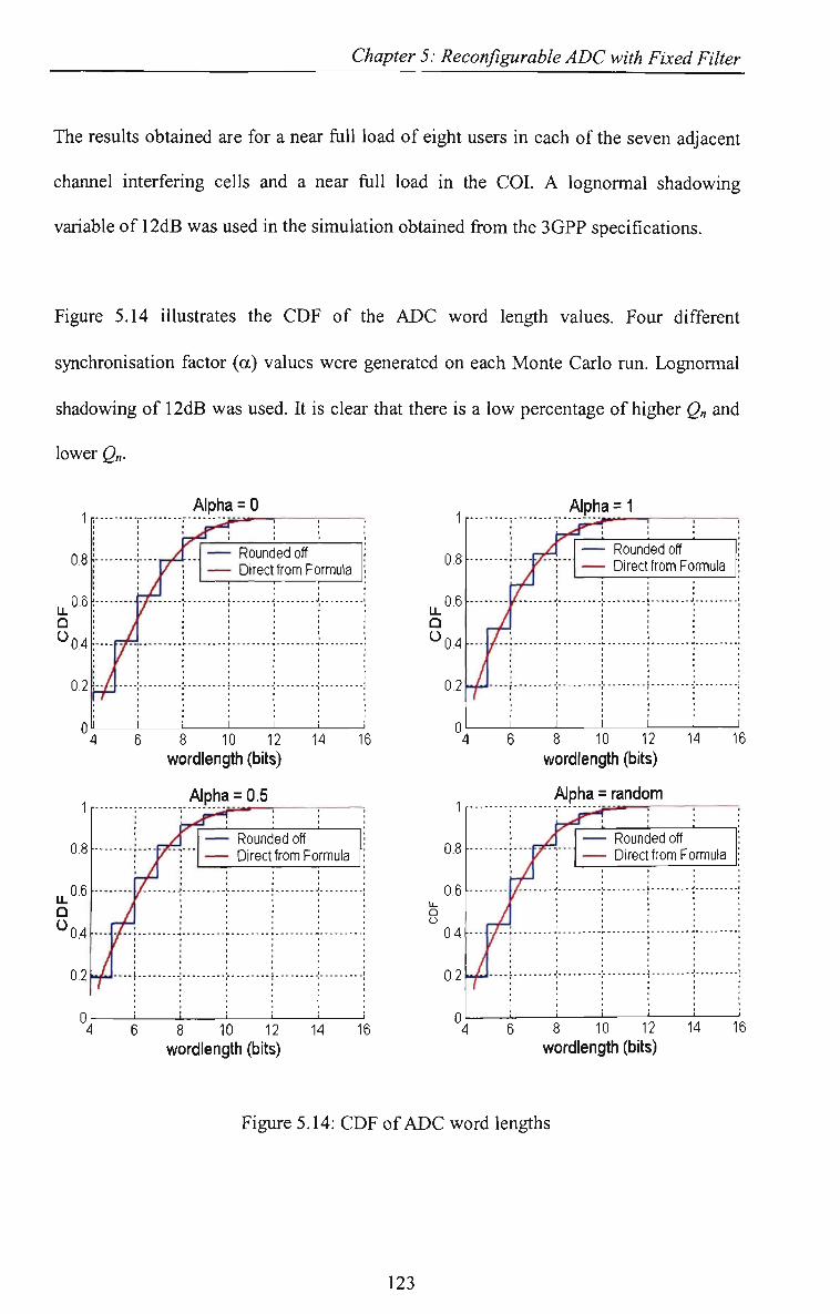
Chapter 5: Reconfigurable ADC with Fixed Filter
The results obtained are for a near fiill load of eight users in each ofthe seven adjacent
channel interfering cells and a near fiill load in the COI, A lognormal shadowing
variable of 12dB was used in the simulation obtained from the 3GPP specifications.
Figure 5,14 illusfrates the CDF of the ADC word length values. Four different
synchronisation factor (a) values were generated on each Monte Carlo run. Lognormal
shadowing of 12dB was used. It is clear that there is a low percentage of higher Q„ and
lower Qn-
LL Q O
1
0.8
0.6
0.4
0.2
Alpha = 0
VfT
M F^
— Rounded off — Direct from Formula
IL Q O
1
0.8
0.6
0.4
0.2 - /
F'
8 10 12 14 16 wordlength (bits)
Alpha = 0.5
— Rounded off — Direct from Formula
^
6 8 10 12 wordlength (bits)
14 16
Alpha = 1
6 8 10 12 14 wordlength (bits)
Alpha = random
16
Rounded off Direct from Formula
6 8 10 12 14 16 wordlength (bits)
Figure 5.14: CDF ofADC word lengths
123

Chapter 5: Reconfigurable ADC with Fixed Filter
Table 5.3 provides a comparison ofthe different median and standard deviation values
for all four different synchronisation factors by using the plots of Figure 5.13.
Table 5,3: Effect on Resolution with different a.
Alpha
a = 0 a = l a = 0,5 a = random
Median Value (bits)
5,897 5,649 5,728 5,764
Standard Deviation
2 2 2 2
From Table 5,3 it can be summarised that even though the difference between the
median values of the resolutions at different alpha values is significantly small, there is
still some percentage of difference. In the implementation process the alpha values will
not affect the resolution due to the rounding off condition. All resolution with decimal
points will have to be rounded off to the higher resolution.
It can be observed in Table 5.3 that when the synchronisation factor a = 0, which means
that there is MS -^ MS interference only, there is a high probability of the required
resolution being between 3,897-bits and 7,897-bits, When a = 1, meaning that there is
only BS -^ MS interference, the probability of required resolution is slightly different to
that when a = 0, and is between 3,649-bits and 7,649-bits, When a = 0,5, meaning that
50 % ofthe interference is from BS ^ MS and 50 % is from MS ^ BS, the probability
of required resolution is between 3.728-bits and 7.728-bits, The final value for a =
random, is when any possibility of interference can occur, and the probability of
required resolution is between 3,764-bits and 7,764-bits,
124
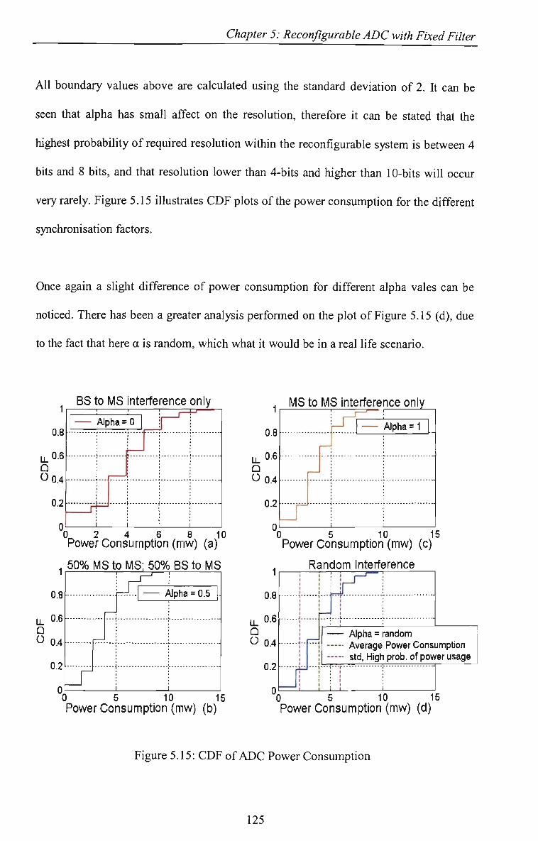
Chapter 5: Reconfigurable ADC with Fixed Filter
All boundary values above are calculated usmg the standard deviation of 2. It can be
seen that alpha has small affect on the resolution, therefore it can be stated that the
highest probability of required resolution within the reconfigurable system is between 4
bits and 8 bits, and that resolution lower than 4-bits and higher than 10-bits will occur
very rarely. Figure 5,15 illustrates CDF plots ofthe power consumption for the different
synchronisation factors.
Once again a slight difference of power consumption for different alpha vales can be
noticed. There has been a greater analysis performed on the plot of Figure 5,15 (d), due
to the fact that here a is random, which what it would be in a real life scenario.
i
0.8
U_0.6 Q O Q . 4
0.2
BS to MS Interference only
Alpha = 0
;'
• 1—H
i i i i L 2_ i % 6 8 10
1
0.8
Power Consumption (mw) (a)
50% MS to MS; 50% BS to MS
u. 0.6 Q O 0.4 [
0.2
0.
Alpha = 0.5
5 10 15 Power Consumption (mw) (b)
1
0.8
U_0.6 Q
O0.4
0.2
0
MS to MS interference only 1 ' ;
I—" — Alpha = 1 ;
i
;
' 0 5 10 15 Power Consumption (mw) (c)
H 1
0.8
U. 0-6 Q O o . 4
0.2
Random Interference
)
J i ^ i 1 ,
1 > \ \ 1 ,
; 1 ;
Alpha = random Average Power Consumption std, High prob. of power usage
i ) 10 1 5 Power Consumption (mw) (d)
Figure 5.15: CDF ofADC Power Consumption
125

Chapter 5: Reconfigurable ADC with Fixed Filter
The last CDF plot of Figure 5,15 (d), shows the power consumption for the entire 16-
bits ADC. The middle dotted line indicates the mean power consumption of the
converter, which is 3,92mW, and is present when the average 6-bits resolution of the
reconfigurable ADC is used. The other two dotted lines surrounding the mean power
consumption dotted line, are the st^idard deviation boundaries, which indicate the
highest probability of power usage of the reconfigurable architecture, which occur
between 1.68mW and 6.16mW, These boundaries correspond to 4-bits and 8-bits. The
results of Figure 5,15 also justify the analysed results illustrated in Figure 5.14.
5.4 Implementation of the Reconfigurable ADC
Prior to illustrating the final layout implementation of the reconfigurable ADC, the
design process, design techniques, and layout considerations are first presented in this
section,
5.4.1 Design Flow and Techniques
This section describes the appropriate CMOS design flow and the circuit design
techniques used for the design and layout ofthe components within the ADC,
5.4.1.1 CMOS IC Design Flow
The CMOS design flow consists of defining circuit inputs and outputs, hand
calculations, schematic entry of design, circuit simulations, layout of the circuit,
simulations including parasitics, re-evaluation of the circuit inputs and outputs, and
finally fabrication and testing. Figure 5,16 [94] illusfrates the CMOS IC design flow.
126

Chapter 5: Reconfigurable ADC with Fixed Filter
This is the general design flow used to design an integrated cfrcuit. More detailed
insight of the design flow used for the design, simulation and layout implementation of
the pipeline ADC is illusfrated in Figure 5,17, The figure illustrates the EDA tools used
to design, simulate, and implement the pipeline ADC, which are supplied by Cadence.
No, Fab Problem No, SpecKtatton Problem
Production
Figure 5,16: CMOS IC design process [97],
At first, the circuits were designed at fransistor level using the Virtuoso Schematic
Editor (Analog Artist), for every component of the ADC, where the designs were
checked and symbol cells for future use were created. The Spectre simulator was used
127
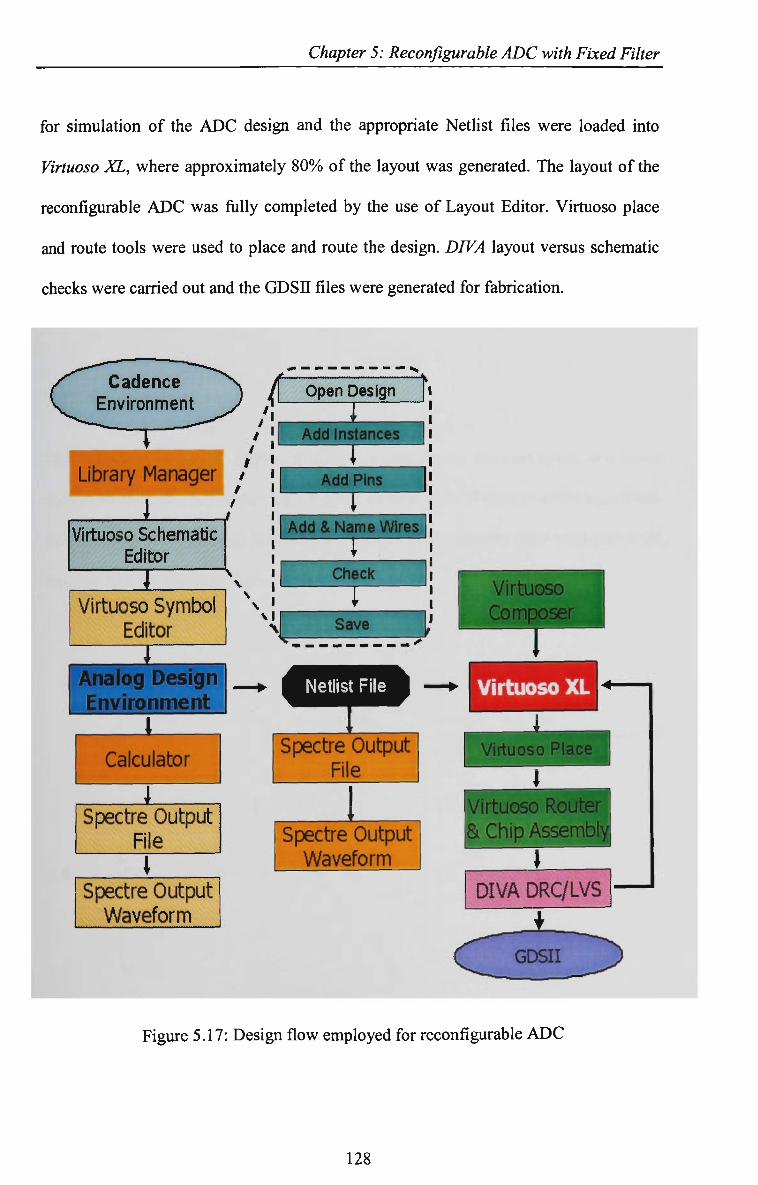
Chapter 5: Reconfigurable ADC with Fixed Filter
for simulation of the ADC design and the appropriate Netlist files were loaded into
Virtuoso XL, where approximately 80% of the layout was generated. The layout of the
reconfigurable ADC was fully completed by the use of Layout Editor. Virtuoso place
and route tools were used to place and route the design. DIVA layout versus schematic
checks were carried out and the GDSn files were generated for fabrication.
.1 Open Design
Add Instances
Library Manager
I Add Pins
Virtuoso Schematic Editor
Add & Name Wires 1
Check
Virtuoso Symbol Editor I
'/dialog Design Environment
i Calculator
1 Spectre Output
File i
Spectre Output Waveform
Save r ^ _ _ _ _ _ _ _ ^ ^
Netlist File
I Spectre Output
File
Spectre Output Waveform
,jpijyjyiu.ijj - I,.. I
Virtuoso Composer 5
Virtuoso XL
ace I
Virtuoso Router Si Chip Assembly
I DIVA DRC/LVS
Figure 5,17: Design flow employed for reconfigurable ADC
128
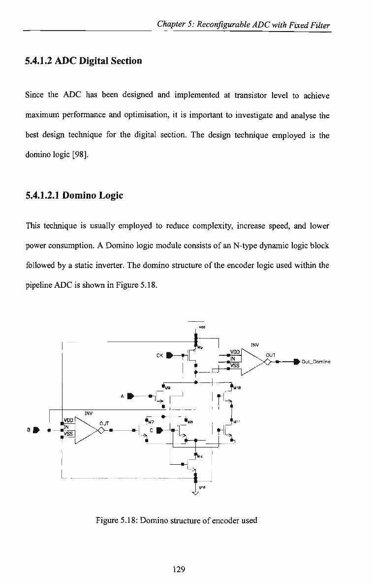
Chapter 5: Reconfigurable ADC with Fixed Filter
5.4.1.2 ADC Digital Section
Since the ADC has been designed and implemented at fransistor level to achieve
maximum performance and optimisation, it is important to investigate and analyse the
best design technique for the digital section. The design technique employed is the
domino logic [98],
5.4.1.2.1 Domino Logic
This technique is usually employed to reduce complexity, increase speed, and lower
power consumption, A Domino logic module consists of an N-type dynamic logic block
followed by a static inverter. The domino structure of the encoder logic used within the
pipeline ADC is shown in Figure 5,18,
> Out_0omino
Figure 5,18: Domino structure of encoder used
129

Chapter 5: Reconfigurable ADC with Fixed Filter
During precharge, the output of the N-type dynamic gate is charged up to VDD and the
output of the inverter is set to 0. During evaluation phase, based on the inputs, the
dynamic gate conditionally discharges and the output of the inverter makes a
conditional fransition from 0 -> 1. The input to a Domino gate always comes from the
output of another Domino gate. This ensures that all inputs to the Domino gate are set to
0 at end ofthe precharge period. Hence, the only possible transition for the input during
the evaluation period is the 0 -> 1 transition. The introduction of the static inverter has
the additional advantage that the fan-out of the gate is driven by a static inverter with a
low-impedance output, which increases noise immunity.
This circuit has the following properties:
• Since each dynamic gate has a static inverter, only noninverting logic can be
implemented,
• Very high speeds can be achieved: only a rising edge delay exists. The static
inverter can be optimised to match the fan-out.
5.4.2 Layout Considerations
In doing layouts for digital circuits, the speed and the area are the two most important
issues. In confrast, in doing layout for analog circuits, performance characteristics such
as speed, area, power consumption and timing, should all be considered simultaneously.
For example, in an amplifier design, good matching in devices is necessary to minimise
the offset voltage, and good shielding is required to protect critical nodes from being
disturbed. Without proper layout, the mismatches and the coupled noise would be quite
large and would significantly degrade the performance ofthe amplifiers.
130
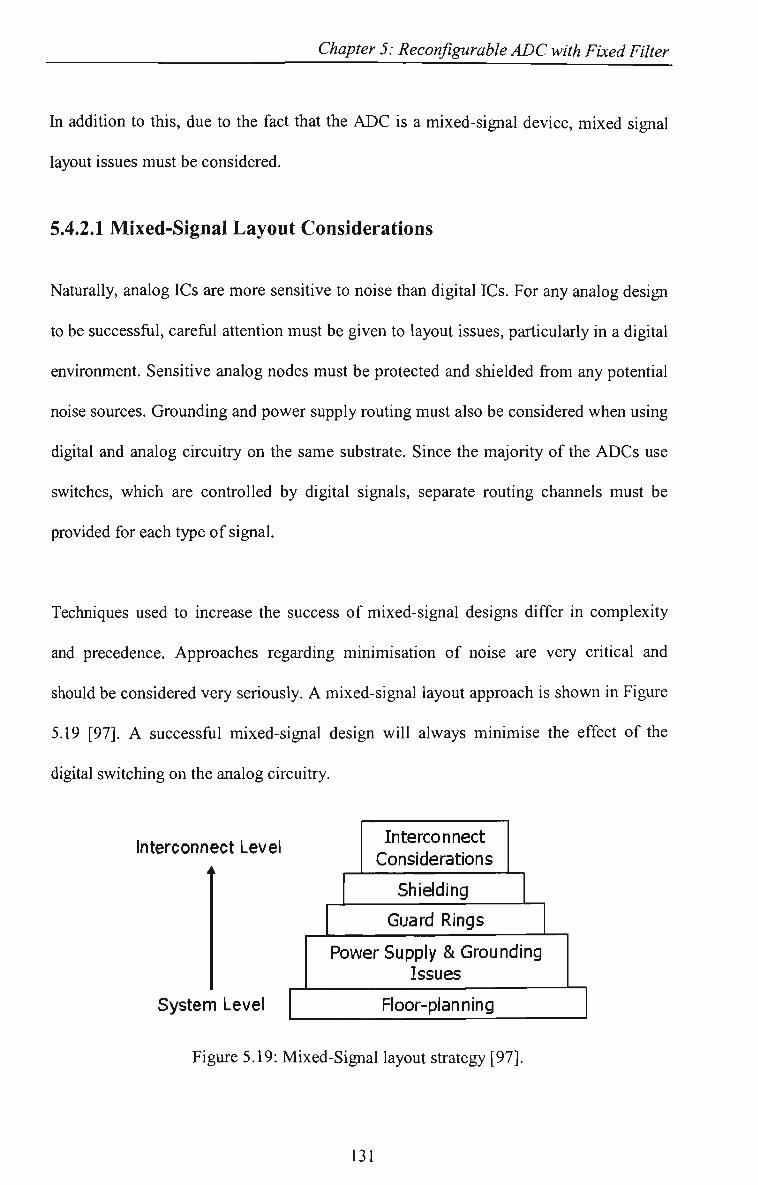
Chapter 5: Reconfigurable ADC with Fixed Filter
In addition to this, due to the fact that the ADC is a mixed-signal device, mixed signal
layout issues must be considered.
5.4.2.1 Mixed-Signal Layout Considerations
Naturally, analog ICs are more sensitive to noise than digital ICs. For any analog design
to be successfiil, carefiil attention must be given to layout issues, particularly in a digital
environment. Sensitive analog nodes must be protected and shielded from any potential
noise sources. Grounding and power supply routing must also be considered when using
digital and analog circuitry on the same substrate. Since the majority of the ADCs use
switches, which are controlled by digital signals, separate routing channels must be
provided for each type of signal.
Techniques used to increase the success of mixed-signal designs differ in complexity
and precedence. Approaches regarding minimisation of noise are very critical and
should be considered very seriously, A mixed-signal layout approach is shown in Figure
5,19 [97], A successfiil mixed-signal design will always minimise the effect of the
digital switching on the analog circuitry.
Interconnect Level
System Level
Interconnect Considerations
Shielding
Guard Rings
Power Supply & Grounding Issues
Floor-planning
Figure 5,19: Mixed-Signal layout sfrategy [97],
131

Chapter 5: Reconfigurable ADC with Fixed Filter
5.4.2.1.1 Floor-Planning
The position of responsive analog instances can greatly affect the performance of a
circuit. Many concerns must be considered. In designing a mixed-signal system,
approaches regarding the floor-plan ofthe circuitry should be analysed before the layout
is to take place. The analog circuitry should be classified by the sensitivity ofthe analog
signal to noise. For example, low-level signals or high impedance nodes typically
associated with the input signals are considered to be sensitive nodes. These signals
should be closely guarded and shielded especially from the digital output pins. High-
swing analog circuits such as comparators and output buffer amplifiers should be
positioned between the sensitive analog circuits and the digital circuits. The digital
circuitry is usually labeled by speed and function. Since digital output buffers are
usually designed to drive capacitive loads at very high speeds, they should be kept as far
as possible from the sensitive analog signals. The high and low speed digital circuits
should be placed between the insensitive analog and the output buffers. Figure 5.20 [99]
illustrates these mixed-signal floor-planning approaches.
Sensitive Analog
Medium-Swing Analog
High-Swing Analog
Low-Speed Digital
High-Speed Digital
Output Drivers
Figure 5.20: Mixed-Signal Floor-Plan [99].
132
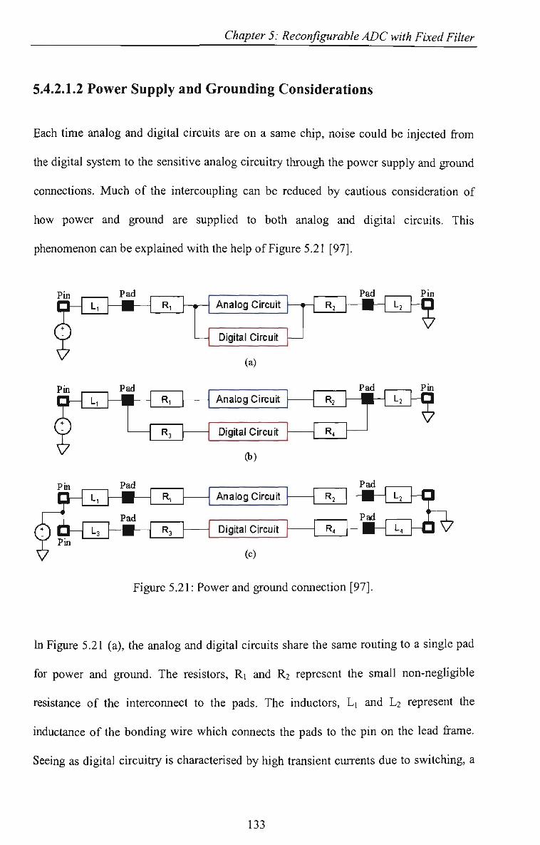
Chapter 5: Reconfigurable ADC with Fixed Filter
5.4.2.1.2 Power Supply and Grounding Considerations
Each time analog and digital circuits are on a same chip, noise could be injected from
the digital system to the sensitive analog circuitry through the power supply and ground
connections. Much of the intercoupling can be reduced by cautious consideration of
how power and ground are supplied to both analog and digital circuits. This
phenomenon can be explained with the help of Figure 5,21 [97],
Pad Analog Circuit
Digital Circuit
Pad , , Pin
(a)
Pad Analog Circuit
Pad
Digital Circuit R4
(b)
Pad Analog Circuit
Digital Circuit R4
Pad
Pad
I 1 ^"^
L. - a ^
(c)
Figure 5.21: Power and ground connection [97].
In Figure 5.21 (a), the analog and digital circuits share the same routing to a single pad
for power and ground. The resistors, Ri and R2 represent the small non-negligible
resistance of the interconnect to the pads. The inductors, Li and L2 represent the
inductance of the bonding wire which connects the pads to the pin on the lead frame.
Seeing as digital circuitry is characterised by high fransient currents due to switching, a
133
Chapter 5: Reconfigurable ADC with Fixed Filter
small amount of resistance associated with the interconnect can result in major voltage
spikes. Low-level analog signals are very sensitive to such interference, therefore
resulting in a impure analog system. One way to reduce the interference, illusfrated in
Figure 5.21 (b), is to exclude the analog and digital circuit from sharing the same
interconnect. The routing for the supply and ground for both the analog and digital
sections are provided separately. Even though this removes the parasitic resistance due
to the common intercormect, there is still a common inductance due to the bonding wire
which still will cause interference.
Another method that minimises interference even more that the method illustrated in
Figure 5,21 (b), is the method shown in Figure 5,21 (c). By using separate pads and
pins, the analog and the digital circuits are completely decoupled. The current through
the analog interconnect is much less sudden that the digital, therefore the analog
circuitry has a so called "quiet" power and ground. However, this technique is
dependent on whether exfra pins and pads are available for this use. It is a wise choice
to use two separate power supplies because if both types of circuits are not powered up
simultaneously, latch-up could easily result.
5.4.2.1.3 Guard Rings
Guard rings should be used wisely throughout a mixed-signal environment. Circuits that
process sensitive signals should be placed in a separate well with guard rings around
that particular circuit. This is usually performed on the analog sections of the chip
layout.
134

Chapter 5: Reconfigurable ADC with Fixed Filter
5.4.2.1.4 Shielding
Number of techniques subsist which can shield sensitive, low-level analog signals from
noise resulting from digital switching. A shield can take the form of a layer tied to
analog ground placed between two other layers, or it can be a barrier between two
signals running in parallel.
If at all possible, one should avoid crossing sensitive analog signals, such as low level
analog input signals, with any digital signals. The parasitic capacitance coupling the two
signal line can be as much as a couple offF, depending on the process. If it can not be
avoided, then attempt to carry the digital signal using the top layer of metal. Another
situation that should be avoided is running interconnect containing sensitive analog
signals parallel and adjacent to any interconnect carrying digital signals. Coupling
occurs due to the parasitic capacitance between the lines. If this situation can not be
avoided, then an additional line connected to analog ground should be placed between
the two signals. This method can also be used to partition the analog and digital sections
ofthe chip,
5.4.3 Reconfigurable ADC Layout
The pipeline ADC top-level block diagram is presented in Figure 5,22, Partitioning is a
critical aspect of layout implementation and must be considered very decisively. The
top level block diagram of the ADC shows all the digital inputs and outputs being at
opposites sides as far away from each other as possible. The maximum resolution for
the ADC is 16 bits where Out 1...Out 16 are the digital output pins, Vin is the analog
input to the ADC, Vref is the input reference voltage, CLK is the clock ofthe system.
135

Chapter 5: Reconfigurable ADC with Fixed Filter
VDD and Vssang are the power supply and ground to the analog section, respectively,
Vdd and Vss_difa.re the power supply and ground to the digital section respectively, Vb
is the bias voltage. Control is the confrol signal that activates which and how many
pipeline blocks need to be tum 'on', and Vres is the final analog output.
CD Q
Vdd
Vss_dig
Control
Outl N Outzi Out 3 Out 4 Outs Out 6 Out 7 Cute Out 9
Out 10 Out 11 Out 12 k Out 13 • Out 14 ]• Out 15 Out 16 V
RECONFIGURABLE ADC
VDD
Vss_ang
Vref
Vb
Vin > z > t— O Q
I CLK
Vres
Figure 5,22: Block Diagram ofADC ASIC
The schematic of the ASIC was designed using the Analog Design Environment tool
from Cadence and simulated using Spectre simulator. The layout of the ADC was
performed on Layout Editor from Cadence using fiill custom 0,18jxm technology.
Figure 5,23 illusfrates the layout ofthe 16-bits ADC.
Once again the ADC layout shows the appropriate partitioning with the analog cells
being separated from the digital cells. A guard ring around the analog section is also
used.
136

Chapter 5: Reconfigurable ADC with Fixed Filter
Guard
Figure 5,23: Layout ofADC
A performance analysis was completed on the ASIC ADC to ensure it meets timing
requirements as well as low power properties. The simulated results are presented in
Table 5.4,
Table 5,4: ADC Performance Results
Parameter
Core Supply Voltage Maximum Clock Frequency with
16 bits resolution Required Clock Frequency for
UTRA-TDD Average Power Consumption
@ 15,36 MHz Average SNR Average DR Critical Path Technology
INL DNL
Core Area
Performance Value
2.5 V 60 MHz
15.36MHz
3,92 mW
37,88 dB 36,12 dB 16,7 nsec
0,18 im CMOS 0,39 LSB 0,43 LSB 0,35mm^
137

Chapter 5: Reconfigurable ADC with Fixed Filter
Figure 5.24 illustrates the dynamic power consumption against the ADC resolution.
Appendix C describes the Cadence power consumption measurement flow.
16
14
§12 c o
| l O 3 CO
8« 6 6 Q.
.a E 4
Power Consumptton of Reconfigurable ADC @ 15,36 MHz
8 10 12 Wordlength (bits)
14 16
Figure 5.24: Dynamic Power Consumption of ASIC components in ADC at 15.36 MHz
It is clear that as the word length increases, the power consumption increases
proportionally. The power consumption ranges from 1.68mW to 15.12mW for word
lengths of 4 bits to 16 bits respectively. The power consumed by the new reconfigurable
ADC architecture can be given by:
P = U^ i
P A. p + p ^BLOCK ^ ^Sl H ^ ^DEC
(16) v % y
where n is the scalable word length, PBLOCK is the dynamic power consumption of a
specific ADC block of ^ bits, PS/H is the power consumed by the front end S/H, and
PDEC is the power consumed by the digital error correction circuit. Table 5,5 tabulates
the power consumption for the variable word length ADC, A maximum power reduction
of 88,89 % has been recorded excluding the DSP control unit, when only 4-bits are
138
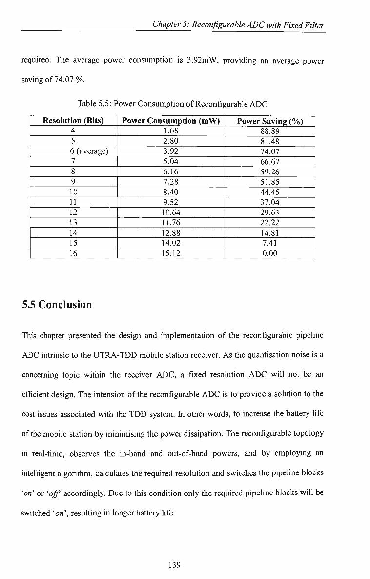
Chapter 5: Reconfigurable ADC with Fixed Filter
required. The average power consumption is 3,92mW, providing an average power
saving of 74,07%,
Table 5,5: Power Consumption of Reconfigurable ADC
Resolution (Bits) 4 5 6 (average) 7 8 9 10 11 12 13 14 15 16
Power Consumption (mW) 1,68 2,80 3,92 5,04 6,16 7,28 8.40 9.52 10,64 11,76 12,88 14.02 15,12
Power Saving (%) 88,89 81,48 74,07 66,67 59,26 51,85 44,45 37.04 29.63 22.22 14,81 7,41 0,00
5.5 Conclusion
This chapter presented the design and implementation of the reconfigurable pipeline
ADC intrinsic to the UTRA-TDD mobile station receiver. As the quantisation noise is a
concerning topic within the receiver ADC, a fixed resolution ADC will not be an
efficient design. The intension ofthe reconfigurable ADC is to provide a solution to the
cost issues associated with the TDD system. In other words, to increase the battery life
ofthe mobile station by minimising the power dissipation. The reconfigurable topology
in real-time, observes the in-band and out-of-band powers, and by employing an
intelligent algorithm, calculates the required resolution and switches the pipeline blocks
'o«' or ''off accordingly. Due to this condition only the required pipeline blocks will be
switched 'on', resulting in longer battery life.
139

Chapter 5: Reconfigurable ADC with Fixed Filter
A sampling frequency of 15.36MHz was used, due to the 3GPP specification, before
down sampling the data by a decimation factor of 4, This was performed due to the
interpolation factor of 4, which is used in the transmitter. The algorithm formulation for
the reconfigurable ADC concluded that three signals are required to determine the
appropriate Qn that gives the overall required resolution. This led to the proposal of the
system architecture presented in Section 5,2,2.
The reconfigurable ADC system consisted of a number of components, namely, pipeline
ADC sti-ucture with resolution switches managed by the control unit, a RRC filter with a
fixed ACP value of 33 dB, a decimation factor of 4 to compromise the interpolation
factor within the transmitter, and a signal power measurement components to provide
clearly varying amplitudes of each three input signals to the control unit. The control
unit calculates the appropriate Qn values and its corresponding bit values. A LUT is then
employed to determine how many blocks ofthe pipeline chain need to be switched 'on'
to provide the required resolution,
A static, statistical analysis on the reconfigurable ADC was performed which in fact
justified the design of a reconfigurable topology. ASIC implementation using O.lS im
technology was performed on the overall reconfigurable ADC, Performance analysis in
terms of power consumption was also presented, showing the significant power saving
ofthe reconfigurable ADC in contrast to a fixed 16-bits ADC,
140

Chapter 6: Effect of Scalable Filter on the Reconfigurable ADC Architecture
Chapter 6
Effect of Scalable Filter on the Reconfigurable ADC Architecture
6.1 Introduction
Chapter 5 presented a reconfigurable pipeline ADC architecture for a mobile terminal
receiver with a fixed filter. The reconfigurable phenomenon of the ADC was provided
by a measure of the quantisation noise (Q„) calculated by an intelligent algorithm of the
confrol unit, resulting in a variable ADC resolution. The inputs to the control unit came
after the filter within the receiver with a fixed ^Ci' of 33 dB. This research is fiirther
extended by combining both the ADC and the RRC filter of the receiver, meaning that
the Qn and the ACP be both variable, to see what effect a scalable filter, with variable
filter lengths would have on the reconfigurable ADC. The motivation for this design is
that the filter in the mobile receiver is also one ofthe major components that consumes
vast amounts of battery power. An optimum balance factor between the ADC and the
filter is found, optimising the power consumption between the two designs. This makes
the architecture power efficient and only consuming minimum power to meet the
signal-to-noise ratio ofthe system.
141

Chapter 6: Effect of Scalable Filter on the Reconfigurable ADC Architecture
The combined reconfigurable architecture (CRA) for an UTRA-TDD mobile terminal
receiver is described in this chapter. The reconfigurable architecture consists of a digital
filter with a variable filter length and a variable word length pipelined ADC, The filter
length and word length depend on the in-band and out-of-band power ratios. When ACI
and co-channel interference (CCI) are low, the required number of filter coefficients
(taps) and word length (bits) of the ADC are reduced which leads to lower power
consumption. This is desirable in battery-powered terminals to increase talk and standby
times. The downlink TDD mode of UMTS UTRA was once again chosen due to its near
far problem to demonstrate the power saving capabilities of this architecture.
Figure 6,1 presents the direct conversion UTRA-TDD mobile terminal receiver, with a
reconfigurable ADC and filter. The control unit accepts three signals (in-band, out-of-
band and desired signal) with clearly varying amplitudes, obtained by the fijll wave
rectifiers and the averaging filters. The basic concept of the combined reconfigurable
architecture is to only utilise the required filter adjacent channel selectivity (ACS) to
meet the required Eb/No. It also assigns any remaining noise available in the system to
quantisation noise ofthe ADC, The concept ofthe filter is similar to that ofthe ADC, If
adjacent channel interference and infra-cell interference powers are low, the ACS ofthe
filter can be reduced and the resolution of the ADC can be decreased to a level that
satisfies the Eb/No, therefore saving battery power. If ACI and infra-cell interference
powers have been increased, then the ACS of the filter and the resolution provided by
the ADC may have to increase in order to meet the Eb/No ratio. Once this is performed,
the control unit calculates the most efficient filter length and ADC word length to
reconfigures the filter and ADC respectively.
142

Chapter 6: Effect of Scalable Filter on the Reconfigurable ADC Architectiire
In-Band Out-of-Band
Modified Control
Unit
• 4 *
Pcwer (Desi red + Co-charhe
LPF (avg)
A. De-
saamble
OSVF^
De-spread
)
CXJt-of-Band Power (AQ)
Desired signal Power
De-mod
data.
Figure 6,1: UTRA-TDD mobile receiver with reconfigurable ADC and Filter
6.2 System Design
The combined reconfigurable architecture is described in this section. The architecture
consists on a number of components to enable a scalable ACP and Qn. Firstly, the filter
considerations are listed and described, containing the filter type and the interference
model ofthe filter.
Secondly, the algorithm enabling the ADC and filter to exploit scalable Qn and ACP
values is formulated and the corresponding system architecture is infroduced. The
subsequent sections describe the analysis ofthe scalable filter, and then the effect ofthe
filter on the reconfigurable ADC is presented and analysed.
6.2.1 Filter Considerations
Digital finite impulse response (FIR) filters can be implemented using various
architectures. The direct form or otherwise known as the transversal structure is the
143

Chapter 6: Effect of Scalable Filter on the Reconfigurable ADC Architecture
most common architecture and is depicted in Figure 6,2 [100], The input, x(n) and the
output yCw) ofthe filter structure are related by:
M
yin) = ^b^»x(n-m) (6,1) m=0
z ' represents a delay unit of one sample or unit of time, thus, x(n-l) is x(n) delayed by
one sample. The output sample is a weighted sum of the present input and M previous
samples ofthe input.
Figure 6,2: Transversal FIR filter structure [100]
The computation of each output sample requires the following hardware [100]:
• M memory locations to store the input samples
• M+1 memory locations to store the coefficients
• M multiplication operations
• M addition operations.
A linear phase structure is a variation ofthe fransversal structure, which takes advantage
of symmetrical coefficients and in effect, uses half the required multiplications and
additions. The only disadvantage is more complex indexing of data is required. For odd
and even phase filters, the fransfer fimction H(z) can be written as [97]:
144

Chapter 6: Effect of Scalable Filter on the Reconfigurable ADC Architectiire
m=o V 2 y
(M+\)l2-\
H{z)= £6„(z-'"-Hz-'"-"') m=0
Modd (6,2)
M even (6,3)
where z' is the filter delay with m varying from 0 to (M/2-1), M is the number of filter
coefficients (taps), and bm is the actual coefficient of the filter. The corresponding
difference equations are as follows [100]:
A//2-1
y{n)= YjKx{m-k) + x{m-{M-k))+b{{M)l2)x{m-{M 12)) Modd (6.4) *=o
A//2-1
y{n)= Y,b^x{m-k) + x{m-{M-k)) Meven (6.5) *=o
where x is the input signal with k varying from 0 to (M2-1). Figure 6.3 [100], illusfrates
the linear phase structure where seven coefficients are used.
x(n) z-i
t, t
+
z-i
+ XJL
'-I
+
b, bj
y(n)
Figure 6,3: Linear Phase FIR filter structure [100]
145

Chapter 6: Effect of Scalable Filter on the Reconfigurable ADC Architecture
Numerous optimisation techniques exist for reducing power dissipation in complex
digital FIR filter implementations for next generation telecommunications equipment
[101-109], These techniques will not reduce it to its most efficient structure as they are
not reconfigurable. In order to even consider the design of a reconfigurable filter, the
ACP and the ASC models must be obtained.
6.2.2 Scalable RRC Filter
This section describes the digital scalable filter. The filter is a pulse-shaping filter with a
FIR, The equation is as follows:
A ' - l
y(n) = Y,x(n-j)-b(]) (6.6)
where y(n) is the filter output sample at 'n', x(n-j) defines the input samples delayed by
y samples, bQ) defines the filter coefficients. A' is the filter length. The impulse
response ofthe pulse-shaping filter is a root-raised cosine (RRC), RCo(t), defined by the
3GPP and given by [96]:
RQ{t)=
f t } t ( t ^ sin ;T—(l-or) +4a—cos ;r—(l + a)
i> J If. V -T
n-T 1- 4a—
T
2\
(6.1)
where the roll-off factor a = 0,22 and Tc is the chip duration of 2.6042e-7 seconds. The
reconfigurable digital filter system block diagram is presented in Figure 6,4. The system
146

Chapter 6: Effect of Scalable Filter on the Reconfigurable ADC Architecture
block diagram presents the basic operation of the filter. The system employs a folded
FIR structure, and shaves off and adds taps to the ends of the impulse response to lower
or raise the stop band dB level. The components in the system are a variable low pass
filter (LPF); high pass filter, two full wave rectifiers, two simple LPF filter networks
and a control unit that determines how many taps are needed to attenuate interference.
As the receiver deals with a complex signal, it may not be necessary to have the confrol
loop on both in-phase (real) and quadrature (imaginary) signals. It may be sufficient for
the in-phase filter to control the tap length for both itself and the quadrature filter.
Therefore, the control unit applies only to the in-phase filter.
i * * -
Inpul output
-^^ ---'
-.._
•—k
— •
LPF
LPF
rcrerrnce
ccrnparB
~ ' •
Control Unit
Figure 6,4: Reconfigurable Digital Filter System
Figure 6.5 shows in detail how the filter taps using the intelhgent control unit algorithm,
are shaved off. The output of the confrol unit is also sent to the ADC to confrol the
resolution. The figure also depicts the operation of the LPFs, resulting in a high pass
signal.
147
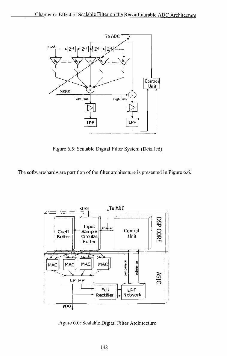
Chapter 6: Effect of Scalable Filter on the Reconfigurable ADC Architecture
To ADC '""T
Figure 6,5: Scalable Digital Filter System (Detailed)
The software/hardware partition ofthe filter architecture is presented in Figure 6,6.
x(n) To ADC
Coeff Buffer
5 ^ = ^
Input Sample Circular Buffer
sha>>er Control
Unh O
o 73
=*^ X MAC MAC
\ / ^ - ,
MAC I
LP HP
RJU Rectifier
LPF Network
n
Yin}
Figure 6,6: Scalable Digital Filter Architecture
148

Chapter 6: Effect of Scalable Filter on the Reconfigurable ADC Architecture
The architecture presents details of the system block diagram. It consists of a DSP core
and an ASIC, The DSP core is used for the control unit, coefficient buffer and input
sample buffer. The ASIC using standard digital libraries consist of four multiply-
accumulate (MAC) units, a LPHP block that outputs the desired low pass and unwanted
high pass signals, a fiill wave rectifier and the LPF networks,
6.2.3 Modified Control Unit
The control unit of the combined reconfigurable architecture required modification in
order to take care of scalable filter lengths as well as reconfigurable ADC resolution.
The modified control unit calculates the appropriate filter length and word length for the
filter and ADC respectively. The equation for the control unit is derived from the signal-
to-noise ratio (SNR) similar to that in [102] and is as follows:
EblNo = ^rx'pg ^ ^^^^
?rx' (M -1) + -^^^^ + rj + Qj ACP' "
where Prx' is the received desired signal power at the i"' MS in the cell of interest (COI).
Processing gain is defined as pg. PrxfM-l) is co-channel interference where M is the
number of users in the COI, The adjacent channel protection factor is defined by CP*,
Thermal noise is given by rj. ItotJ is the ACI signal received. It is mathematically
represented as:
^ total ~ 2^ j 7=1 '^ B„ (6.10)
149

Chapter 6: Effect of Scalable Fiher on the Reconfigurable ADC Architecture
where K^B„ is the path loss between the/ ' ' adjacent channel BS causing interference and
the mobile located at m in the COI, M^ is the number of users served by the/* BS. Pt*/
is the/*^ adjacent BS transmission power. Qn' is remaining noise in the system and is
defined as the quantisation noise:
a ' = G , . ^ (6.11)
where Gk is a gain control factor balancing Qn and ACP. If Gk is set to zero, the ACP'
will be at a minimum, therefore leaving no margin of error for Qn. Solving for ACP
results in:
1+ J^^ ?Tx' -7]-?rx'M EbINo
where Prx'M is the in-band signal. The actual attenuation of the filter is referred to as
adjacent channel selectivity (ACS). The ACS depends on the Adjacent Charmel Leakage
Ratio (ACLR) as well as the ACP requirement. The ACLR is the ratio ofthe transmitted
interference power to the power measured after a receiver filter in the out-of-band
channels. The relationships have been investigated in [110] and it is found that:
ACS'=^^ ^ — 1 ~ ( - ^^
ACP' ACLR
From Equation 6,13 it is clear that the ACP factor will be scaled higher as the ACI is
scaled by a factor of (Gk+l). Hence, if the Eb/No ratio is calculated, it will be higher
than the target allowing the difference to be utilised as quantisation noise. With the new
150

Chapter 6: Effect of Scalable Filter on the Reconfigurable ADC Architecture
calculated value for the ACP, the quantisation noise can be calculated in the control unit
as in Equation 6,11, This confrol unit accepts the three inputs, similar to the conttol unit
of chapter 5, and by using appropriate algorithms, it determines how many taps or bits
are required to be shaved off or added on to ensure the Eb/No is met at all times. The
control unit now sends a shaver signal to the coefficient and input sample buffer
adjusting their pointers with an offset. The shaver signal switches taps 'on' or 'off in
the FIR structure. It is defined as:
. t e v . r = ^ ' " ^ - ^ ' - ^ ^ " ^ - ^ " (6.14) 2
where Max/iength is the maximum filter length available and Newjiength is the new
calculated filter length. For example, if Newjiength is 19 and Maxjiength is 65, the shaver is
then set to 23, Therefore, 23 taps from each end of the impulse response will be
switched off and the other will be switched on. It also sends a signal to the ADC that
control how many blocks need to be activated. The changes take place for the next
frame input to the filter. The new tap length will also apply to the quadrature filter. The
feedback is performed constantly per frame to ensure the minimum number of taps and
bits are used. Figure 6.7 presents numerous frequency response plots of the pulse-
shaping filter as taps are shaved off the tails of its impulse response. The LUT
employed in the confrol unit that takes care of the reconfigurable filter is illustrated in
Table 6,1, where the filter length ranges from 5 to 65 taps with a margin of 4 in between
them. The LUT acquires the corresponding shaver value with the calculated ACP factor
and after each sample, the filter will reconfigure its value. Concurrently, the resolution
ofthe ADC is also being reconfigured.
151

Chapter 6: Effect of Scalable Filter on the Reconfigurable ADC Architecture
Frequency (Hz)
Figure 6,7: Frequency Response using various filter lengths
Table 6,1: Modified Control Unit Look-Up Table for Filter
ACP (dB)
44,8 < & < 44.9 44,7 < & < 44,8 44,5 < & < 44,7 43,8 < & < 44,5 43,6<&<43.8 43,2 < & < 43,6 42.0 < & < 43.2 38,8 < & < 42
36,4<&<38,8 34,6 < & < 36,4 29,8 < & < 34.6 27 < & < 29.8 25 < & < 27 20 < & < 25 1 4 < & < 2 0
<14
ACS (dB)
60 58 56 54 50 49 48 45 40 37 35 30 27 25 20 14
Filter Length
65 61 57 53 49 45 41 37 33 29 25 21 17 13 9 5
Filter Shaver
0 2 4 6 8 10 12 14 16 18 20 22 24 26 28 30
152

Chapter 6: Effect of Scalable Filter on the Reconfigurable ADC Architecture
Further analysis on the inter symbol interference ofthe filter was required to determine
what should be the minimum filter length to ensure the Eb/No requirement is met, A
base band transceiver simulation model was created to measure the effect of shaving
taps off with respect to inter symbol interference (ISI), The specifications for this
simulation model are presented in Table 6,2,
Table 6.2: Base Band Transceiver Parameters
Parameter
Number of users
OSVF Code length
Bit rate
MS Rx RRC Filter roll off factor
BS Tx RRC Filter roll off factor
# of taps in Tx RRC Filter
Value
8
16
16 Kbps
0,22
0,22
41
Analysis shows that as taps are shaved off the filter, there is an increase in error vector
magnitude (EVM) when analysing the received symbols. This leads to an increase in
ISI, which is defined as:
ISV =lO-log,o(mea«(£FM(«)^)J (6.15)
where EVM is a vector of n samples andy corresponds to a certain filter length. Figure
6,8 presents the results of the ISI analysis. Overall, the ISI reduces when the filter
153

Chapter 6: Effect of Scalable Filter on the Reconfigurable ADC Architecture
length increases as expected. However, the reduction is not smooth because certam filter
lengths have better ISI than others. The required signal-to-noise ratio for adequate
performance is 6,5dB (2 * Eb/No) for a QPSK modulator, obtained by usuig an Eb/No
of 3,5dB, specified by the 3GPP, ISI power should be made much less than -6,5dB if it
is not to affect the noise performance of the receiver. An additional safety margin of
20dB to take care of any additional interference in the system would be acceptable,
resulting in -26,5dB of ISI, Therefore, acceptable filter lengths are all the froughs in
Figure 6,8 under -26,5dB, such as 5, 11, 13 and > 19, The minimum filter length is 5,
Filter Taps vs. Inter Symbol Interference
-15
-20
-25.
-30
-35
2 . -40
-45
-50
-55
-60
-66
I — i — I 1 1 1 1 1 1 \ 1 1 I \ I I I I I I I I I I
10 15 20 26 30 Filter Taps
35 40 45 50
Figure 6,8: Inter-Symbol Interference Analysis
Based on the above algorithm the structure ofthe reconfigurable ADC with a scalable
filter is illusfrated in Figure 6,9,
154

Chapter 6: Effect of Scalable Filter on the Reconfigurable ADC Architecture
RF Signal. Pipeline '
Block 13 ^"^^' res
Modified Control
Unit
In-Band Power y(n)
-* De-mod
data,
Out-of-Band Power (AC!)
Desired signal Power
Figure 6.9: Combined Reconfigurable Architecture (CRA)
6.3 Statistical Analysis
A statistical analysis ofthe CRA, in a static environment to see the effect ofthe scalable
filter on the reconfigurable ADC is presented in this section. The analysis divulges the
efficiency of the CRA in the UTRA-TDD environment. The analysis on the CRA
provides an estimated power consumption savings in percentages, as compared to a
fixed ADC and filter structure. Simulation parameters for this design are listed in Table
6.3.
155

Chapter 6: Effect of Scalable Filter on the Reconfigurable ADC Architecture
Table 6,3: Simulation Parameters
Parameter
Standard deviation, a (dB) Gain Factors, Gk
Bit Rate Max TX Power (dBm) Thermal Noise (dBm) Required Eb/No (dB)
Receiver Sensitivity, without Imargin (dBm) Cell Radius (m)
# of Interfering Adjacent Cells # of users in each Interfering
Adjacent Cell Synchronisation factor a
Path loss exponent y
Value
12 0,001,0,1,0,5,1,2,4,6,8, 10
32 Kbits/s Downlink: 10, Uplink: 4
-102.85 3,5
-112,89
100 7 8
Uniform random 0 to 1 3,0
A range of gain factors, Gk, values are used to achieve a comparison between the
averages of the ADC resolution and the RRC filter ACP factors, A lognormal
shadowing variable standard deviation of 12 dB is employed as per statistical analysis
ofthe reconfigurable ADC presented in chapter 5, Figure 6,10 illustrates the CDF ofthe
filter ACP factors and the ADC resolution by Monte Carlo simulations of equation 6.12
and the bit value («') equation shown as:
10»logl0
n =
^ (ACT + Pr x') • Decimationp ^
6.02 + Safety M
(6,16)
where ACT is the adjacent channel interference, DecimationF is the decimation factor of
4, specified by the 3GPP, Qn is the quantisation noise of the system, and SafetyM is a
safety margin employed to take care of some large spikes at the input. The analysis
presented is for Gk values of 0.001 to 2, Figure 6,11 illusfrates the results for Gk values
156

Chapter 6: Effect of Scalable Filter on the Reconfigurable ADC Architecture
between 4 and 8. Table 6,4 corresponds to the recorded results of the figures where the
mean and standard deviation are listed.
C D F of A D C Resolution C D F of ACP Factor 1
0.9
0.8
0.7
0.6
U-Q 0 . 5 o
0.4
0.3
0.2
0.1
0
' , ^ ;n ,U '^ ;^ - l - ^ Imr-"'^^
1 / _ . . L m..f....
•7/ / " i 7// 7
i l\ /
! —
'
W> 1 1
1 /
Gk = 0.001 Gk = 0.1 Gk = 0.5 Gk = 1 Gk = 2
i 10 15
Resolution (bits) -20 0 20 40
A C P (dB) 60
Figure 6,10: Statistical analysis of CRA (Gk = 0,001 ^ 2)
CDF ofADC Resolution
Resolution (bits) (a)
CDF of Filter ACP Factors
-20 0 20 40 60 ACP(dB) (b)
Figure 6,11: Statistical analysis of CRA (G t = 4 ^ 10)
157

Chapter 6: Effect of Scalable Filter on the Reconfigurable ADC Architecture
Table 6,4: Statistical analysis results of CRA
Gain Factor, Gk
0,001 0.1 0,5 1 2 4 6 8 10
Mean (Bits) (dB)
11,3780 8,2394 7,2403 7,0099 6,8000 6,6401 6,6120 6,5980 6,5280
STD (Bits) (dB)
1,5094 1,6481 1,6214 1,6798 1.6300 1,6151 1.6043 1,6484 1,6060
Mean (ACP) (dB)
18.7144 19,7445 20,4441 22,0846 24.0559 26,0641 27,5431 28,8137 29,2661
STD (ACP) (dB)
12,2275 12.2294 12,6426 12,7245 12.1208 12.1137 12,3882 12,2289 12,1542
The lowest gain factor of 0,001 presents the most efficient case for the mean, M, of
ACP factors, but the least efficient case for mean of bits. The reason for this is because
there is only a slight increase of the availability of quantisation noise of the ADC,
corresponding to a necessarily higher dynamic range of the ADC, On the other hand the
mean of the ACP is lower as it has only been adjusted by a very small gain, A gain
factor of Gk= 10, presents the most efficient case for the mean ofthe ADC resolution,
but the least efficient case for the mean of the filter ACP factors. This case is the
opposite ofthe first case, when Gk = 0,001, as the ADC requires lower dynamic range
whereas the filter needs a greater ACP factor to take the edge off the ACI. A G* = 0,001
is suitable as it makes the filter efficient but the ADC not efficient as the mean
resolution is significantly high and reconfigurable approach has no advantage. On the
other hand, when G* = 10, the ADC benefits from the reconfigurable approach, as the
resolution is low, but the filter in this case has no benefit.
The standard deviation of the ACP factors and the ADC resolution does not vary
significantly as expected. The gain factor Gk should only have dramatic effects in the
means due to the fact that the ACP factors are scaled by a gain, A 0,5289 dB variation in
158

Chapter 6: Effect of Scalable Filter on the Reconfigurable ADC Architecttire
the standard deviation for the ACP factors has been recorded and 10% variation in the
ADC resolution,
A suitable gain factor which provides a good balance between the efficiency of the
ADC and filter where the mean resolution is 6.8-bits and the mean ACP factor is
12,1208 is a Gk value of 2, Gain factors between 0,001 and 2 also decrease the mean of
the ADC resolution by 40%, which is considered to be a dramatic improvement,
whereas the mean is only improved by 4% when gain factors between 2 and 10 are
used. Therefore, there is no need to increase Gk beyond a gain factor of 2, It is also
essential to note gain factors greater than 2 will result in the same mean in terms ofthe
ADC resolution, concurrently unnecessarily decreasing the efficiency of the filter.
Figure 6,12 depicts the statistical analysis ofthe ADC resolution and filter tap length
respectively.
1
0.9
0.8
0.7
0.6 U-Q 0 . 5 O
0.4
0.3
0.2
0.1
O
C D F Of A D C R e s o l u t i o n 1
0.9
0.8
0.7
0.6 Ll_ Q 0 . 5 O
0.4
0.3
0.2
0.1
C D F o f F i l te r L e n g t h
J—+1 __ L i _
10 15 Resolut ion (bits)
20 40 Filter Lengtf i
60
Figure 6.12: Statistical analysis of CRA (Gk = 2)
159
Chapter 6: Effect of Scalable Filter on the Reconfigurable ADC Architecture
The filter lengths were obtained using the LUT, Table 6.1, and the ADC resolutions
were obtained using the LUT, Table 5,1,
The average ADC resolution when compared to the reconfigurable ADC of chapter 5
with a fixed ACP factor is increased by 1 bit to 7-bits, This outcome corresponds to a
56% efficiency savings for the ADC, when compared to a maximum ADC resolution of
16-bits, and a 73% efficiency savings for the filter, compared to the 3GPP
specifications. The efficiency will correspond to foremost and essential power
consumption savings in both devices, the ADC and filter in the CRA,
6.4 Conclusion
In chapter 5, a reconfigurable ADC architecture with a fixed filter length was presented.
The effect of scalable filter on the reconfigurable ADC is presented in chapter 6,
A reconfigurable approach to extend battery life in the mobile station by minimising
power consumption has resolved cost issues in the receiver ADC, This combined
reconfigurable architecture (CRA) monitors the in-band and out-of-band signal powers
and intelligently calculates the required ACP factor, which in fact corresponds to a
certain filter length (taps). The system design led to the proposal ofthe system structure,
which consists ofthe reconfigurable pipeline ADC architecture in chapter 5, as well as
the filter structure. The filter is a pulse-shaping filter with a finite impulse response. The
impulse response of the pulse-shaping filter is a root-raised cosine. The system employs
this folded FIR structure, and shaves off and adds taps to the ends of the impulse
160

Chapter 6: Effect of Scalable Filter on the Reconfigurable ADC Architecture
response to lower or raise the stop band dB level. This is performed by the system
confrol unit. As the mobile receiver deals with a complex signal, it may not be
necessary to have the control loop on both in-phase (real) and quadrature (imaginary)
signals. It may be sufficient for the in-phase filter to control the tap length for both itself
and the quadrature filter. Therefore, the control unit applies only to the in-phase filter.
The control unit in the CRA calculates the required dynamic range of the ADC and the
corresponding ACP factor ofthe filter, and by employing LUTs it determines how many
ADC stages and filter taps need to be tumed 'on' or switch 'off, in order to provide the
required resolution and ACS respectively.
The efficiency of the ADC and filter have been dramatically affected by various gain
factors in search for the ultimate trade off between the two architectures, A gain factor
of 2 was found to provide the right balance of efficiency between the ADC and filter, A
statistical analysis provided an average ADC resolution of 7-bits and an average filter
length of 13. This offers a 56% power savings for the ADC and 73% saving for the
filter. These results are for an UTRA-TDD indoor environment in a static simulated
domain. The confrol unit was modified to take into account the safety margin
protection, but hysteresis was not considered. Simulations in a dynamic domain, where
hysteresis is considered, will not affect the average ADC resolution because the
quantisation noise is calculated before the protection takes effect, but it might very well
increase the filter length.
161
Chapter 7: Conclusions & Future Work
Chapter 7
Conclusions & Future Work
7.1 Introduction
During the last decade, wireless communications have been the inspiration behind
analog electronics development. By the emergence of new communication standards
comes an ever increasing signal bandwidth, allowing more services to be provided.
Concurrently, the limits between digital and analog signal processing is impending
closer to the antenna, therefore aiming for a software-defined radio solution. In terms of
ADCs of mobile terminal receivers, this indicates higher sample rate, lower power
consumption and higher resolution.
This chapter presents the final remarks on the major research findings, along with some
assumptions used through out the research. The chapter is concluded with some fiiture
work ideas for an extension on the present findings.
162
Chapter 7: Conclusions & Future Work
7.2 Major Findings
The objectives of this research together with the corresponding fmdmgs are listed
below:
• Design and implementation of a Modified-Flash ADC (Sub-ADC) architectures:
The Sub-ADC is the most critical component ofthe pipeline ADC architecture. Making
the right choice of which topology to employ is highly dependent on the design
appUcation, In this research, power consumption was of greatest concem due to the
UTRA-TDD application. The standard flash design can operate at high frequencies, but
it consumes large power due to the high design complexity and high device count.
Therefore modification to the standard flash design has been carried out in order to
compromise between power consumption and speed requirement.
Analysis on the UTRA-TDD system was performed in terms of its dynamic range in
order to find out the resolution of the first pipeline block. From the dynamic analysis
performed, it was concluded that for an enhancement of 6.02 dB of interference, an
additional 1-bit must be added. Therefore, the reconfigurable design consisted of 13
pipeline blocks. The first being a 4-bit block followed by 12 1-bit blocks. The first
block of the pipeline ADC, which uses a modified-flash architecture was presented in
chapter 4, It requires only (2^"^^ + 2) comparators to implement the modified N-bit flash
ADC, This approach greatly reduced the complexity and size ofthe full flash ADC and
the two-step flash ADC, The new ADC architecture dissipates only 1.68 mW of power
at 15.36 Ms/s as compared to a full flash ADC of 6,5 mW and a two-step flash of 2,39
mW, Results indicate that a 74% power saving is obtained and 53% of die size could be
163
Chapter 7: Conclusions & Future Work
saved when the modified flash ADC is used instead ofthe fiill flash architecture, as die
sub-ADC ofthe first pipeline chain.
• Design and implementation of a Pipeline ADC architectures:
It was found that there are distinct advantages of using the pipeline ADC topology as
compared to its counterparts. While the flash ADC architecture can reach very high
speed, it consumes a lot of power due to the high device count. The other ADC
architectures consume little power, but they operate at very low speeds, which are not
appropriate for the UTRA-TDD application, where the 3'"'' generation system
specification of 15,36 Ms/s needs to be met.
However, even though fix word-length pipeline ADC architecture could be suitable for
the mobile receiver, it still has a distinct disadvantage when it comes to power
consumption. In many cases a fixed word-length ADC is used, say 12-bits, when the
receiver requires and uses a converter of only 8-bits, During this time the whole 12-bit
device is powered up, which uses a lot more power than it is supposed to. To achieve
this, a more complex receiver ADC design and implementation is required, which will
have a significant impact on battery life in the mobile terminal.
ADC optimisation techniques could lower power consumption but will not reduce it to
its most efficient level, A solution in theory is to use minimum resolution, and still meet
the performance requirements of the UTRA-TDD receiver specified by the 3GPP, To
achieve this, in-band and out-of-band signal powers were measured. The ADC
intelligently choses the amount of resolution required to ensure the out-of-band signal is
164

Chapter 7: Conclusions & Future Work
below a certain tolerance level and the SNR is still met. This scheme vastly reduced
power consumption, as it only utilises the required resolution as compared to traditional
fixed complexity architectures.
The translation from theory into reality was obtained by taking advantage of the
software radio concept and technologies. Taking advantage ofthe software radio theory,
a solution was achieved using DSP and ASIC technologies that can meet the
performance and system needs of high speed and low cost devices.
• Design and implementation of a Reconfigurable ADC architecture:
Chapter 5 presented the design and implementation of the reconfigurable pipeline ADC
intrinsic to the UTRA-TDD mobile station receiver. The intension of the reconfigurable
ADC was to provide a solution to the cost issues associated with the TDD system. The
reconfigurable topology in real-time, observes the in-band and out-of-band powers, and
by employing an intelligent algorithm, calculates the required resolution and switches
the pipeline blocks 'on' or 'off accordingly,
A sampling frequency of 15.36 MHz was used, due to the 3GPP specification, before
down sampling the data by a decimation factor of 4, This was performed due to the
interpolation factor of 4, which is used in the fransmitter. The algorithm formulation for
the reconfigurable ADC concluded that three signals are required to determine the
appropriate Qe that gives the overall required resolution. The formulation led to the
proposal of the system architecture. It consisted of a number of components;
reconfigurable pipeline ADC structure, a RRC filter with a fixed ACP value of 33 dB, a
165
Chapter 7: Conclusions & Future Work
decimation factor of 4 to compromise the interpolation factor within the transmitter, and
a signal power measurement components to provide clearly varying ampUtudes of each
three input signals to the control unit. The control unit calculated the appropriate Qn
values and its corresponding bit values, A LUT was then employed to determine how
many blocks of the pipeline chain were required to be switched 'o«' to provide the
required resolution,
• Statistical analysis ofthe UMTS system:
A static, statistical analysis on the reconfigurable ADC was also performed and
presented in chapter 5, which in fact justified the design of a reconfigurable ADC, ASIC
implementation using 0,18^m CMOS technology was performed on the overall
reconfigurable ADC. Performance analysis in terms of power consumption and noise
was also presented, showing the significant power saving of the reconfigurable ADC in
contrast to a fixed 16-bits ADC. A CDF plot ofthe reconfigurable ADC with a random
synchronisation factor indicated that the average resolution of the converter is 6,
resulting in 3,92mW of power consumption,
• Effect ofthe scalable filter on the reconfigurable ADC architecture::
The effect ofthe scalable RRC filter on the reconfigurable ADC architecture inherent to
the UTRA-TDD mobile station receiver was presented in chapter 6. The analysis of this
architecture was an extension of the reconfigurable ADC presented and analysed in
chapter 5 to see the effect ofthe RRC filter on the ADC and cater for power efficiency
in the digital filter, A reconfigurable approach to extend battery life in the mobile
station by minimising power consumption had resolved cost issues in the receiver ADC,
166

Chapter 7: Conclusions & Future Work
This CRA monitored the in-band and out-of-band signal powers and inteUigently
calculates the required ACP factor, which in fact corresponds to a certain filter length
(taps). The system design led to the proposal of the system structure, which consists of
the reconfigurable pipeline ADC and filter architecture.
The efficiency of the ADC with a scalable filter was dramatically affected by various
gain factors in search for the ultimate trade off between the two architectures. A gain
factor of 2 was found to provide the right balance of efficiency between the ADC and
filter. A statistical analysis provided an average ADC resolution of 7-bits and an
average filter length of 13, This offers a 56% power savings for the ADC and 73%
saving for the filter. These results were for an UTRA-TDD indoor environment in a
static simulated domain. The control unit was modified to take care ofthe safety margin
protection, but hysteresis was not considered. Simulations in a dynamic domain, where
hysteresis is considered, did not affect the average ADC resolution because the
quantisation noise is calculated before the protection takes effect. However, the CRA
provides a proficient approach to deal with cost concerns intrinsic to the UTRA-TDD
mobile station receiver,
7.3 Assumptions
The statistical results presented in this thesis are based on computer simulations in
MATLAB, Therefore, they are limited with a set of assumptions. The analysis was
based on static simulations, which provided a good insight into the UTRA-TDD system
with respect to the sensitivity and how certain system parameters affect the analysis.
The performance of UTRA-TDD is greatly dependant on a certain set of parameters
167

Chapter 7: Conclusions & Future Work
such as Eb/No targets, cell structure and cluster geometry, processing gain and thermal
noise. Varying these parameters will accordingly vary the results of the analysis
especially if the Eb/No is changed.
Handover was also not assumed in the simulations where handover might improve the
statistical analysis results. In addition, the same bit rate for each user was assumed. In
practice, a time slot can be fully loaded by one user with high data rates. This case also
improves the results as intra-cell interference will not be severe. The analysis was
limited to one downlink time slot and only considered the +5 MHz adjacent channel.
Considering other adjacent channels (-5 MHz and ±10 MHz) will have an impact on the
results. It can be said that the results in the analysis are based on certain parameters and
do not apply to all scenarios. Nevertheless, a good insight is provided with a static
statistical analysis,
7.4 Future Work
Wireless transmission is weakened by signal fading and interference. The increasing
requirements on data rate and quality of service for wireless communications systems
call for new techniques to increase spectrum efficiency and to improve link reliability.
The analysis in this thesis used a single-input single-output antenna, to present the
reconfigurable phenomenon. The use of multiple antennas at both ends of a wireless
link promises significant improvements in terms of specfral efficiency and link
reliability. This technology is known as multiple-input multiple-output (MIMO)
wireless system, and is illusfrated in Figure 7,1,
168

Chapter 7: Conclusions & Future Work
It would be an interesting task to employ this reconfigurability to the MIMO system,
where the SNR of the system would be at a more accurate level as compared to the
smgle-input single-output scenario.
T X
I T
o o
T H
1 T
o o
T R X
Figure 7,1: Schematic representation of a MIMO wireless system
Employing handover within the system will also improve the statistical analysis results.
Handover is the mechanism that transfers an ongoing call from one cell to another as a
user travels through the coverage area of a cellular system. As smaller cells are
developed to meet the demands for an increased capacity, the number of cell boundary
crossing increases. Each handover requires network resources to re-route the call to a
new base station. Minimising an expected number of handovers decreases the switching
load. The design of reliable handover algorithm is critical to the operation of a cellular
communications system and especially important in micro-cellular systems where the
mobile receiver may traverse several cells during a call. The improvement to the
statistical results in the UTRA-TDD scenario will happen as there is less adjacent
mobiles within the cell of interest, there will be less transmission power, therefore less
interference. As it has been presented in this thesis, if the interference is low, then the
ADC resolution is low. If handover is not present, as the case in this thesis, there is
more fransmission power from base station to mobile, therefore more interference to the
receiver.
169

Chapter 7: Conclusions & Future Work
Another interesting scenario worth while investigating in order to reduce power besides
tuning the resolution ofthe proposed architecture is to employ voltage scalmg. Some of
the components within the system do not require the full scale voltage of 2,5 volts to do
their required operation, they may only need 1.5 volts or 2 volts to operate, therefore
DC-DC converters could be used to scale the voltage down and/or up. Obviously power
consumption is proportional to the supply voltage, therefore components operating at
lower supply voltages will have less power consumption, resulting in reduction of
power and longer battery life ofthe mobile terminal.
170

BibUographv
Bibliography
[1] "IEEE Standards for Terminology and Test Methods for Analog-to-Digital Converters, Standards, Measurements", IEEE Standard 1241-2000, 2000,
[2] L, Sumanen, M, Waltari, K, Halonen, "An 8-bit 40MS/s Pipeline A/D Converter for WCDMA Testbed", Analog Integrated Circuits and Signal Processing, vol,22, no.l, pp,41-49, 2000,
[3] W, T. Colleran, A, A, Abidi, "A 10-b, 75-MHz Two-Stage Pipelined Bipolar A/D Converter", IEEE J. of Solid State Circuits, vol,28, no. 12, pp,1187-1199,1993,
[4] K, Sone, Y. Nishida, N, Nakadai, "A 10-b 100-Msample/s Pipelined Subranging BiCMOS ADC", IEEE J, of Solid State Circuits, vol,28, no, 12, pp,l 180-1186, 1993,
[5] F, Murder, R. Gosser, "12b 40 Msamples/s Two-Stage A/D Converter", hit'l Solid State Circuits Conference, San Francisco, pp, 216-217, 1995,
[6] B, Nauta, A, G, W, Venes, "A 70 Msamples/s 110 mW 8b CMOS Folding Interpolating A/D Converter", Int'l Solid State Circuits Conference, San Francisco, pp,214-215, 1995,
[7] Y, Akazawa, A, Iwata, T, Wakimoto, T. Kamato, H, Nakamura, and H, Dcawa, "A 400 MSPS 8 b flash AD conversion LSI," in IEEE fritemational SoUd-State Circuits Conference, pp, 27-28, 1987.
[8] Maxim Editors "Pipeline A/D converters come of age", Maxim Engineering Journal, vol.33, pp.3-9, 1999,
[9] T, B, Cho, P, R, Gray, "A 10 b, 20 Msample/s, 35 mW pipeline A/D converter", IEEE J, of Solid State Circuits, vol,30, pp,166-172, 1995,
171

Biblio graph V
[10] J, Sevenhans, Z, Y, Chang, "A/D and D/A Conversion for telecommunication", IEEE Circuits & Devices, pp,32-42, 1998,
[11] M, Ito et al,, "A 10 bit 20 MS/s 3v supply CMOS A/D converter for integration into system VLSIs", ISSCC Dig, Tech. Papers, pp,48-49, 1994,
[12] M, Ito et al„ "A 10 bit 20 MS/s 3v supply CMOS A/D converter", IEEE J, of Solid State Circuits, vol,29, pp,1531-1536, 1994.
[13] Fujimori, K. Koyama, "A 5 v Single-Chip Delta-Sigma Audio A/D Converter with 111 dB Dynamic-Range", IEEE Custom Integrated Circuits Conference, pp,415-418,1996.
[14] T, Burger, Q, Huang, "A 13,5-mW 185-Msample/s A-S Modulator for UMTS/GSM Dual-Standard IF Reception", IEEE J. of Solid State Circuits, vol,36, no, 12, pp, 1868-1878, 2001.
[15] P, Ferguson, et al,, "An 18b 20KHz dual delta-sigma A/D converter", in Proc, ISSCC, pp.68-69, 1991,
[16] K, Falakshahi, C-K, K, Yang, B. A. Wooley, "A 14-bit, 10-Msamples/s D/A Converter Using Multibit S-A Modulation", IEEE J. of Solid State Circuits, vol,34, no,5, pp,607-615, 1999.
[17] S-I, Liu, C-H. Kuo, R-Y, Tsai, J, Wu, "A Double-Sampling Pseudo-Two-Path Bandpass A-Z Modulator", IEEE J, of Solid State Circuits, vol.35, no,2, pp,276-280, 2000,
[18] B, P, Brandt, J, Lutsky, "A 75-mW, 10-b, 20-MSPS CMOS Subranging ADC with 9.5 Effective Bits at Nyquist", IEEE J, of Solid State Circuits, vol.34, no,12,pp,1788-1795, 1999,
[19] K, Kusumoto, A, Matsuzawa, K, Murata, "A 10-b 20-MHz 30-mW Pipelined hiterpolating CMOS ADC", IEEE J, of Solid State Circuits, vol,28,no.l2,pp, 1200-1206, 1993,
[20] Mehr, L, Singer, "A 55-mW, 10-bit, 40-Msample/s Nyquist-Rate CMOS ADC", IEEE J, of Solid State Circuits, vol. 35, no. 3, pp. 318-325, 2000,
[21] Y-T Wang, B, Razavi, "An 8-bit 150-MHz CMOS A/D Converter", IEEE J, of Solid State Circuits, vol, 35, no. 3, pp, 308-317, 2000,
[22] S, A, Paul, H-S Lee, J, Goodrich, T. F. Alailima, D, D, Santiago, "A Nyquist-Rate Pipelined Oversampling A/D Converter", IEEE J, of Solid State Circuits, vol, 34, no, 12, pp, 1777-1787, 1999,
[23] A, M, Abo, P, R, Gray, "A 1.5V, 10-bit, 14,3-MS/s CMOS Pipeline Analog-to-Digital Converter", IEEE J, of Solid State Circuits, vol,34, no,5, pp,599-
172
BibUographv
605, 1999.
[24] E, Opris, B, C, Wong, S. W. Chin, "A pipeline A/D Converter Architecttu-e with Low DNL", IEEE J. of SoUd State Circuits, vol,35, no,2, pp,281-285, 2000,
[25] Y, Ren, B, H, Leimg, Y, M, Lin, "A mismatch-independent DNL pipelined analog-to-digital converter", IEEE Trans. Cfrcuits Symp, n, vol. 46, pp, 517-526, 1999.
[26] I. E, Opris, L, D, Lewicki, B, C. Wong, "A single-ended 12-bit 20 MS/s self calibrating pipeline A/D converter", Int'l Solid State Circuit Conf, pp. 138-139, 1998,
[27] R, H, Walden, "Analog-to-Digital Converter Survey and Analysis", J, on Selected Areas in Communications, vol.17, no,4, pp,539-550, 1999,
[28] L, Sumanen, M, Waltari, K, Halonen, "A 10-bit 200-MS/s Parallel Pipeline A/D Converter," IEEE J, Solid-State Circuits, vol, 36, no. 7, pp, 1048-1055, 2001,
[29] W. Yang, D, Kelly, I, Mehr, M. T, Sayuk, L. Singer, "A 3-V 340-mW 14-b 75- Msample/s CMOS ADC with 85-dB SFDR at Nyquist hiput", IEEE J. Solid-state Circuits, vol, 36, no. 12, pp. 1931-1936, Dec, 2001,
[30] W. Yang, D, Kelly, I, Mehr, M. T. Sayuk, L. Singer, "A 3-V 340-mW 14-bit 75-Msamples/s CMOS ADC with 85-dB SFDR at Nyquist hiput", IEEE J. Solid State Circuits, vol,36, no. 12, pp. 1931-1936, 2001.
[31] D. A, Johns, K, Martin, Analog Integrated Circuit Design, John Wiley & Sons, New York 1997,
[32] J, Goes, J, C, Vital, J, E, Franca, "A CMOS 4-bit MDAC with Self-Calibrated 14-bit Linearity for High-Resolution Pipelined A/D Converters," in Proceedings of the IEEE Custom Integrated Circuits Conference (CICC'96), pp, 105-108, 1999,
[33] J, Guilherme, P, Figueiredo, P, Azevedo, G, Minderico, A, Leal, J. Vital, J. Franca, "A Pipehne 15-b 10-Msample/s Analog-to-Digital Converter for ADSL Applications," in Proceedings of the IEEE Int, Symposium on Circuits and Systems (ISCAS' 01), pp, 1-396-399, 2001,
[34] R, Gregorian, G, C. Temes, "Analog MOS fritegrated Circuits for Signal Processing", John Wiley & Sons, Singapore, 1986,
[35] M, Waltari, Circuit Techniques for Low-Voltage and High-Speed A/D Converters, Doctoral Thesis, Helsinki University of Technology, 2002,
173

BibUographv
[36] D. W, Cline, P, R, Gray, "A Power (Optimized 13-b 5 Msamples/s Pipelined Analog-to-Digital Converter in l,2[im CMOS," IEEE J. SoUd-State Cfrcuits, vol, 31, no, 3, pp, 294-303, Mar. 1996,
[37] K, Poulton, R, Neff, A, Muto, W, Liu, A, Bumstein, M. Heshami, "A 4GSamples/s 8b ADC in 0,35pm CMOS", IEEE hit, SoUd State Cfrcuits Conference Digest of Technical Papers, pp, 166-167, 2002,
[38] K, Sockalingham, "Error Compensation in Pipeline A/D Converters", Masters Thesis, University of Maine, 2002.
[39] T, Cho, "Low-Power Low-Vohage Analog-to-Digital Conversion Techniques Using Pipelined Architectures", Memo-randum no, UCB/ERL M95/23, 2 April 1995,
[40] R. Zimmermann and W, Fichtner, "Low-Power Logic Styles: CMOS Versus Pass-Transistor Logic", IEEE Journal of SoUd-State Circuits, vol, 32, p. 1079-1090, July 1997.
[41] A, N, Karanicolas, H, S, Lee, and K, L. Barcrania, "A 15b IMS/s digitally self calibrated pipeline ADC", ISSCC Dig, Tech Papers, pp, 60-61, 1993,
[42] C, S, G, Conroy, "A high-speed parallel pipeline A/D converter technique in CMOS", Memorandum No, UCB/ERL M94/9, Electronics Research Laboratory, U, C. Berkeley, February 1994.
[43] D, W, Cline, "Noise, Speed and Power Trade-offs in Pipelined Analog to Digital Converters",Memorandum No. UCB/ERL M95/94, Elecfronics Research Laboratory, U,C, Berkeley, November 1995.
[44] T. B. Cho, G, Chien, F, Brianti, and P, R, Gray, "A Power-Optimized CMOS Baseband Channel Filterand ADC for Cordless Applications," Symposium On VLSI Circuits, June 1996,
[45] T, B, Cho and P. R, Gray, "A lObit, 20MS/s, 35mW Pipeline A/D Converter," Proc, IEEE Custom Integrated Circuits Conference, pp 23,2,1-23,2,4, 1994.
[46] K. Sockalingam and R. Thibodeau, "Design and Layout of a lObit 5MHz Pipeline A/D Converter", University of Maine, Dept. of Electiical and Computer Eng,, Orono, Maine, VLSI Design Report, 2002,
[47] K. Gulati, H,S. Lee, "Low Power Reconfigurable Analog-to-Digital Converter", IEEE Journal of Solid Stare Circuits, vol. 36, issue 12, 1900-1911,2001.
174

BibUographv
[48] Povey, G, J, R,, Nakagawa, M, "A review of Time Division Duplex -CDMA techniques" Proceedings of ISSSTA'98 International Symposium on Spread Spectrum Techniques and Applications, Vol,2,, pp. 630-633,1998.
[49] Povey, G, J, R, 'Time Division Duplex - Code Division Multiple Access for Mobile Multimedia Services' IEEE Conference Proceedings of 8th International Symposium on Personal, Indoor and Mobile Radio Communications - PIMRC '97, Vol,3., pp, 1034-1037, 1997,
[50] 3rd Generation Partnership Project, 'Technical Specification Group Radio Access Networks; Physical Layer - General Description 3G TS 25,201 version 3,0.2', 2000,
[51] R. Rummler, A. H. Aghvami, 'End-to-end IP multicast for software upgrades of reconfigurable user terminals within IMT-2000/UMTS networks' IEEE International Conference on Communications, ICC 2002, pp,502-506,2000,
[52] Guerrero, L. O,, Aghvami, A, H. 'Capacity Assessment for UTRA' IEEE 49th Vehicular Technology Conference. Moving Into a New Millennium, Vol, 2,pp, 1653-1657, 1998,
[53] W, Mohr, 'UTRA FDD and TDD, a harmonized proposal for IMT-2000' International Conference on Communication Technology ICCT'98, pp, SS22-03-1 - SS-22-03-5, 1998,
[54] Ojanpera, T,, and Prasad, R,, 'WCDMA: Towards IP Mobility and Mobile Internet' Artech House, 2001,
[55] T, Ojanpera and R, Prasad, 'An overview of Air Interface Multiple Access for IMT-2000/UMTS', IEEE Communications, pp, 82-95,1998.
[56] 3rd Generation Partnership Project, 'Physical Channels and Mapping of Transport Channels onto Physical Channels (TDD)' TS 25,221, version 3.2.0, 2000.
[57] 3rd Generation Partnership Project, 'Technical Specification Group Radio Access Networks; Spreading and Modulation (TDD) 3G TS 25,223 version 3,2,0', 2000,
[58] 3rd Generation Partnership Project. 'Technical Specification Group Radio Access Networks; UTRA (BS) TDD; Radio Transmission and Reception 3G TS 25,105 version 3,2,0', 2000,
[59] 3rd Generation Partnership Project, 'Technical Specification Group Radio Access Networks; UTRA (UE) TDD; Radio Transmission and Reception 3G TS 25,102 version 3,2,0', 2000.
175

BibUographv
[60] ETSI 30,03, "Universal Mobile Telecommunications System (UMTS); Selection procedures for choice of radio transmission technologies of the UMTS" V3,2,0, TR 101 112,1998,
[61] H, Haas, S, McLaughlin and G.J.R, Povey, "The Effects of friterference between the TDD and FDD mode in UMTS at the boundary of 1920MHz", IEEE 6* Internal Symposium on Spread Spectrum Technologies, 2000.
[62] H, Heikkinen, H, Haas, G,J,R, Povey, "Investigation of Adjacent Channel Interference in UTRA-TDD System", lEE Colloquium on UMTS Terminals and Software Radio, 1999,
[63] W, Yang, D, Kelly, I. Mehr, M, T, Sayuk, L, Singer, "A 3-V 340-mW 14-b 75-Msample/s CMOS ADC With 85-dB SFDR at Nyquist hiput," IEEE Journal of Solid-State Circuits, vol, 36, pp, 1931-1936, December 2001,
[64] K, Y, Kim, N. Kusayanagi, A. A. Abidi' A 10-b, 100-MS/s CMOS A/D Converter, IEEE Journal of Solid State circuits, 32(3), 1997.
[65] P, Petschacher et al, A 10-b 75-MSPS Subranging A/D Converter with Integrated Sample and Hold, IEEE Journal of Solid State Circuits, 25, 1339-1346, 1990,
[66] A, Boni, A, Pierazzi, C, Morandi, "A 10-b 185-MS/s Track-and-Hold in 0,35-nm CMOS," IEEE Journal of SoUd-State Circuits, vol, 36, pp, 195-203, February 2001,
[67] A, S, Sedra, K, C. Smith, "Microelectronic Circuits", Third Edition, Saunders CoUage Publishing, 1991.
[68] P, Real, D. Mercer, "A 14b Linear, 250 nsec Sample-and-Hold Subsystem with Self-Calibration", ISSCC Dig. Tech. Papers, pp. 164-165, 1991,
[69] B, Razavi, "Priciples of Data Conversion System Design", Workshop on Advances in Analog Circuit Design, Austiia, April 1995,
[70] R, Poujois et al, "Low-level fransistor amplifier using storage techniques", in ISSCC Dig, Tech, Papers, pp, 152-153, 1973,
[71] J, Doemberg, P, R, Gray, D, A. Hodges, "A 10-bit 5-Msample/s CMOS two-step flash ADC", IEEE Journal of SoUd State Circuits, vol, 24, pp,241-249, 1989,
[72] S. Chin, M, K, Mayes, R, Filippi, "A multistep ADC family with efficient architectinre", ISSCC Dig, Tech, Papers, pp. 16-17, 1989,
[73] P, J. Crawley, G, W, Roberts, "Designing Operational Transconductance Amplifiers for Low Voltage Operation," IEEE International Symposium on
176

BibUographv
Circuits and Systems, pp, 1455-1458, 1993.
[74] L, Sumanen, M, Waltari, K, Halonen, "Optimizing the Number of Parallel Channels and the Stage Resolution in Time Interleaved Pipelme A/D Converters," in Proceedings of the IEEE Int, Symposium on Circuits and Systems (ISCAS'2000), pp, V-613-616, 2000,
[75] K, Bult, G. Geelen, "A Fast Settling CMOS Op Amp for SC Circuits witii 90-dB DC Gain," IEEE J. SoUd-State Circuits, vol, 25, no, 12, pp, 1379-1384, Dec, 1990,
[76] J, Bastos, A, Marques, M, Steyaert, and W. Sanson, "A 12 -Bit Intrinsic Accuracy High-Speed CMOS DAC," IEEE Joumal of Solid State Circuits, Vol, 33, No, 12, 1998,
[77] R, R, Neff, P, R, Gray, and A, Sangiovanni -VincentelU, "A Module Generator for High-Speed CMOS Current Output Digital/Analog Converters", IEEE J, of Solid State Circuits, Vol.31, No,3, 1996,
[78] Chi-Hung Lin and Klaas BuU, "A 10-b, 500-MSample/s CMOS DAC in 0,6 mm 2", IEEE J, of SoUd-State Circuits, Vol, 33, No, 12, December 1998,
[79] D. Johns and K, Martin, Analog Integrated Circuit Design, ch, 8, John Wiley & Sons, hic, 1997,
[80] P, R, Gray, P, J, Hurst, S, H, Lewis, R, G, Meyer, "Analysis and Design of Analog Integrated Circuits", 4"" Edition, John Wiley & Sons, 2001,
[81] B, M. Wilamowski, D. L. Jordan, O. Kaynak, "Low Power Current Mode Loser-Take-All Circuit for Image Compression", 9" NASA Symposium on VLSI Design, New Mexico, pp. 7,6,1 - 7,6,8, 2000.
[82] IEEE Standard for Terminology and Test Methods for Analog-to-Digital Converters, Standard, Measurements," IEEE Standard 1241-2000, Dec. 2000,
[83] R, van de Plasshe, Integrated Analog-to-Digital and Digital-to-Analog Converters, Kluwer Academic Publishers, Dordrecht, 1994,
[84] PureBits,com "Measurement of SNR, THD, THD+N and IMD" http://www,purebits,com/appnote8.html AppUcations notes 8, 2003,
[85] M. Keramat, N, Kehtamavaz "DSP System Design using the TMS320C6000", Prentice Hall, 2001,
[86] Kalle Folkesson, Jan-Erik Eklund, Christer Svensson, Andreas Gustafsson, "A Matlab-based ADC Model for RF System Simulations" GHz 2000 Symposium, Gothenburg, Sweden, March 13-14, 2000,
177

BibUographv
[87] B. Razavi, "Principles of Data Conversion System Design", John Wiley & Sons, January 1995,
[88] P. G. Gray and R, G, Meyer, Analysis and Design of Analog Integrated Circuits: Second Edition, John Wiley & Son fric, 1984,
[89] G, Knoblinger, P, Klein, M, Teibout, "A New Model for Thermal Channel Noise of Deep-Submicron MOSFETS and its Application in RF-CMOS design", IEEE J, of SoUd-State Circuits, vol, 36, no, 5, 2001.
[90] J. S, Goo, S. Donati, C, H. Choi, Z. Yu, T. H. Lee, and R. W. Dutton, "Impact of Substrate Resistance on Drain Currene Noise in MOSFETs", Proceesings of SIP AD, 2001,
[91] E, Kreyszig, "Advanced Engineering Mathematics", Seventh Edition, John Wiley & Sons, hic, 1993,
[92] 3'''' Generation Partnership Project, TSGRAN, 'UTRA (UE) TDD; Radio Transmission and Reception' 3G TS 25,102, version 3,2,0, 1999
[93] H, Haas, "Interference analysis of and dynamic channel assignment algorithms in TD-CDMA/TDD systems", PhD Thesis, University Of Edinburgh, Scotland, 2000,
[94] Zysko, J,A,, and Lane, J.E., 'Infinite Impulse Response Filters for Postprocessing Noisy Field Test Data', Technical report, Kennedy Space Center, NASA and Dynacs hic, 2001. http://technologv.ksc.nasa.gov/WWWaccess/techreports/2001report/500/508.htm
[95] 3rd Generation Partnership Project (3GPP), Technical Specification Group (TSG), Radio Access Network (RAN), Working Group 4 (WG4), "Evaluation of up- and downlink adjacent channel performance" TSGR4#2(99) 048, February 1999,
[96] 3' ' Generation Partnership Project, 'Technical Specification Group Radio Access Networks; Spreading and Modulation (TDD) 3G TS 25,223 version 3,2.0', 2000,
[97] R. J, Baker, H, W, Li, D, E, Boyce, "CMOS Circuit Design, Layout, and Simulation", IEEE Press Series on Microelectronic Systems, Wiley and Sons fric. PubUcation, 1998,
[98] J, M, Rabaey, ''Digital Integrated Circuits - A Design Perspective", Prentice Hall, 1996,
[99] Y, Tsividis, "Mixed Analog-Digital VLSI Devices and Technology: An Infroduction", McGraw-Hill PubUshing Co., 1996,
178

BibUographv
[100] E, C, Ifeachor, and B. W, Jervis, 'Digital Signal Processing: A Practical Approach' Addison Wesley, 1993,
[101] R, Paako, et al, 'A new Algorithm for Elimination of Common Subexpressions', IEEE Trans, On Computer - Aided Design of Integrated Circuits and Systems, Vol, 18, no,l, Jan. 1999.
[102] A, G, Dempster, N, P. Murphy, 'Efficient interpolators and filter banks using muUiplier blocks' IEEE Transactions on Signal Processing, Vol. 48 Issue, 1, pp, 257-261, 2000.
[103] M, Potkonjak, et al,, 'Multiple Constant Multiplications: Efficient and Versatile Framework and Algorithms for Exploring Common Subexpression Elimination', IEEE Transactions on Computer-Aided Design of Integrated Circuits and Systems, Vol, 15, no,2, Feb. 1996.
[104] T. G. Noll, 'Carry-Save Arithmetic for High-Speed Digital Signal Processing', Joumal of VLSI Digital Signal Processing, Vol. 3, pp. 121-140, 1991.
[105] Y. C. Lim, 'Frequency-Response Masking Approach of Sharp Linear Phase Digital Filters', IEEE Transactions on Circuits and Systems, Vol. CAS-33, no,4, April 1986.
[106] T. Saramaki, Y, Neuvo, and S, K, Mitra, 'Design of Computationally Efficient Interpolated FIR filters', IEEE Transactions on Circuits and Systems, Vol, 35, no,l, Jan, 1988,
[107] T, Saramaki, H, Johansson, 'Optimization of FIR filters using the frequency-response masking approach' IEEE fritemational Symposium on Circuits and Systems, ISCAS, pp 177-180, 2001.
[108] D. R, Bull, and H, Horrocks, 'Primitive Operator Digital Filter Synthesis Using a Shift Biased Algorithm'. Intem. Symposium on Circuits and System, ISCAS, 1998.
[109] Z, Jing, and A, T. Fam, 'A New Sti^cture for Narrow Transition Band, Lowpass Digital Filter Design', IEEE Transactions on Acoustics, Speech and Signal Processing, Vol. ASSP-32, no.2, 1984.
[110] 3'"'' Generation Partnership Project (3GPP), Technical Specification Group (TSG), Radio Access Network (RAN), Working Group 4 (WG4), "Evaluation of up-and downlink adjacent channel performance", TSGR4#2(99) 048, 1999,
179

Appendix A: Spreading & Modulation in TDD
Appendix A
Spreading & Modulation in TDD
This documentation is taken directly from the 3' ' Generation Partnership Project
(3GPP), technical specification group radio access network, 3G TS 25,223, V3,3.0, This
document describes multiplexing, channel coding and interleaving for UTRA Physical
Layer TDD mode,
A.l General Information
In the following, a separation between the data modulation and the spreading
modulation has been made. The data modulation is defined in section A,2 and the
spreading modulation in section A,3,
Table A,l: Basic modulation parameters
Chip rate
Data moduiation Spreading cliaracteristics
Basic chiprate: 3.84 Mcliip/s
QPSK Ortliogonai
Q ciiips/symboi, wfiere Q = 2", 0 <= p <= 4
Low cliiprate: 1.28 Mchip/s
QPSK Orthogonai
Q chips/symboi, wliere Q = 2", 0 <= p <= 4
180

Appendix A: Spreading & Modulation in TDD
A.2 Data modulation
A.2.1 Symbol rate
The symbol duration Ts depends on the spreading factor Q and the chip duration Tc:
Ts = Q X T„ where Te = ^ ^
A.2.2 Mapping of bits onto signal point constellation
A.2.2.1 Mapping for burst type 1 and 2
The data modulation is performed to the bits from the output of the physical charmel
mapping procedure and combines always 2 consecutive binary bits to a complex valued
data symbol. Each user burst has two data carrying parts, termed data blocks:
d(*''>=(j|*''>,4*''),...,4''>)^ i = l,2;k = l,...,K. -yv^ (A.1 )
Nk is the number of symbols per data field for the user k. This number is linked to the
spreading factor Qk as described in table A.l. Data block d *'' is transmitted before the
midamble and data block d *' ^ after the midamble. Each ofthe A'* data symbols d}y^;
i=\, 2; k=l,.„,K; n=l,„,,Nk; of equation 1 has the symbol duration T^''^=Qk.Tc as afready
given.
The data modulation is QPSK, thus the data symbols ^ *'' are generated from two
consecutive data bits from the output ofthe physical channel mapping procedure in [8]:
181

Appendix A: Spreading & Modulation m TDD
bj'^/^ e {0,1} / = 1,2; k = \,...K; n = 1,...,/V ; / = 1,2 (A.2)
Using the following mapping to complex symbols:
Table A,2: Mapping to Complex Symbols
consecutive binary bit pattern
»r*r 00 01 10 11
complex symbol
—n
+i +1 -1
-j
The mapping corresponds to a QPSK modulation of the interleaved and encoded data
bits bj^f^ of equation 0,
A.2.2.2 Mapping for PRACH burst type
In case of PRACH burst type, the definitions in subclause 5,2,1 apply with a modified
number of symbols in the second data block. For the PRACH burst type, the number of
96 symbols in the second data block d *' ^ is decreased by Q^ symbols.
A.3 Spreading modulation
A.3.1 Basic spreading parameters
Spreading of data consists of two operations: Chaimelisation and Scrambling, Firstly,
each complex valued data symbol rf^*''^ of equation 1 is spread with a real valued
channeUsation code c * of length g e {1,2,4,8,16}, The resulting sequence is then
scrambled by a complex sequence v of length 16,
182

Appendix A: Spreading & Modulation in TDD
A.3.2 Channelisation codes
, W , i . _ The elements c ; k=l,„,,K; q=l,...,Qk; ofthe real valued channeUsation codes
c cc, ,C2 ,-,CQ^) _ j^^j^ J..
shall be taken from the set
V ={1,-1} (A,3)
.(*) The c ^ are Orthogonal Variable Spreading Factor (OVSF) codes, allowing to mix in
the same timeslot channels with different spreading factors while preserving the
orthogonality. The OVSF codes can be defined using the code tree of Figure A,l.
c ^=' =(l,l) Q=2 ^ ' ^
^'P = (U,U)
c«-'>=(l)
c - ^ =(1,1,-1,-1)
c^*='^=(l-l)
c^:;>=(i,-u-i)
c ;-> =(1,-1,-1,1)
Q=l Q = 2 Q=4
Figure A.l: Code-tree for generation of Orthogonal Variable Spreading Factor (OVSF) codes for Channelisation Operation
Each level in the code free defines a spreading factor indicated by the value of Q in the
figure. All codes within the code tree caimot be used simultaneously in a given timeslot.
A code can be used in a timeslot if and only if no other code on the path from the
specific code to the root ofthe free or in the sub-free below the specific code is used in
183
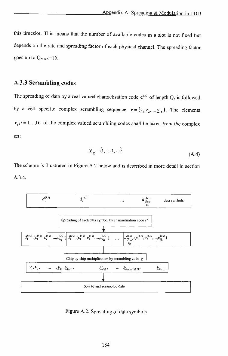
Appendix A: Spreading & Modulation in TDD
this timeslot. This means that the number of available codes in a slot is not fixed but
depends on the rate and spreading factor of each physical channel. The spreading factor
goesuptoQMAx=16,
A.3.3 Scrambling codes
The spreading of data by a real valued channelisation code c * of length Qk is followed
by a ceU specific complex scrambling sequence Y = (v,,V2'-'Zi6)- The elements
v,.;i = 1,..,,16 ofthe complex valued scrambling codes shall be taken from the complex
set:
Y^={l,j,-l,-j} (A,4)
The scheme is illustrated in Figure A.2 below and is described in more detail in section
A.3,4,
/ ( * , ' • ) j(*.0 SMAX
a data symbols
Spreading of each data symbol by channelisation code c***
Mkj) ( (k,i) (*,/) „(k.i)\j(k,n (M.i) (*,/) (* ,0N " I •^''1 f^2 '•••>'-Q, J " 2 -V^l »'-2 »—>^a )
MkJ) (JkJ) (kj) (kj).^ QMAX
a
Chip by chip multiplication by scrambling code y
Y.^Yi, ••-a'-a+i' »i:f2a' — 'i'a^^-a+i' —yuAx
Spread and scrambled data
Figure A,2: Spreading of data symbols
184

Appendix A: Spreading & Modulation in TDD
In Equation A.4 the letter j denotes the imaginary unit, A complex scrambling code y is
generated from the binary scrambling codes v =(vp v2,-,v,g) of length 16 shown in
Annex A, The relation between the elements y and v is given by:
li =(j)' -v,. v. G{l , - l i i = l,...,16
Hence, the elements v,. of the complex scrambling code y are altemating real and
imaginary. The length matching is obtained by concatenating QMAX/QU spread words
before the scrambling,
A.3.4 Spread signal of data symbols and data blocks
The combination of the user specific channelisation and cell specific scrambling codes
can be seen as a user and cell specific spreading code s *' =\s^p^) with
(*) _ (*)
..I(.-.)n,odeJ ,k=l,...,K,p=l,...,N,Q,.
With the root raised cosine chip impulse filter Cro(t) the transmitted signal belonging to
the data block d *'' of equation 1 transmitted before the midamble is
^A Qk
i'\t)=Y,£''^ ^.;„%^^^.Cr„(/-(v-l)7;-(«-l)a7;) " = i <?=' (A.6)
and for the data block d *' ^ of equation 1 transmitted after the midamble
Nk Qk
d_^'^>\t)= Y.^y^ Y.'V-\)Qk+q-^'^^^-^'i-^^'^C-(n-mkTc-NkQkTc-LmTc)-n=l 9=1 (A. 7)
where Lm is the number of midamble chips.
185

Appendix A: Spreading & Modulation in TDD
A.3.5 IModulation
The complex-valued chip sequence is QPSK modulated as shown in Figure A,3 below. COSM)
Complex-valued s chip sequence
Split real& Imag. parts
Re{S) Pulse-shaping
InHS} Pulse-shaping 13
-sin(cot)
Figure A, 3: Modulation of complex valued chip sequences
A.4 Synchronisation codes
A.4.1 Code Generation
The Primary code sequence, Cp is constmcted as a so-called generalised hierarchical
Golay sequence. The Primary SCH is furthermore chosen to have good aperiodic auto
correlation properties.
Define a = <xi,X2,X3, ...,xi6> = < l , 1, 1, 1, 1, 1,-1,-1, 1,-1, 1,-1, 1,-1,-1, 1 >
The PSC code word is generated by repeating the sequence 'a' modulated by a Golay
complementary sequence and creating a complex-valued sequence with identical real
and imaginary components.
The PSC code word Cp is defined as Cp=< y(0),y(l),y(2)„..,y(255) >
where j ; = (l-f j)x < a,a,a,-a,-a,a,-a,-a,a,a,a,-a,a,-a,a,a >
and the left most index corresponds to the chip fransmitted first in each time slot.
The 16 secondary synchronization code words, {Co,...,Ci5 } are complex valued with
identical real and imaginary components, and are constmcted from the position wise
multiplication of a Hadamard sequence and a sequence z, defined as:
186

Appendix A: Spreading & Modulation in TDD
z= <b,b,b,-b,b,b,-b,-b,b,-b,b,-b,-b,-b,-b,-b > , where
h=<x^,...,x,,-x,,...,-x^, > = <l, 1,1,1,1,1,-1,-1,-1,1,-1,1,-1,1,1,-l>.
The Hadamard sequences are obtained as the rows in a matrix H^ constmcted
recursively by:
Ho = (1)
, k>l Hk=\"'-' ^ * - . ^ Hk-\ - - ^ i - i y
The rows are numbered from the top starting with row 0 (the all zeros sequence).
Denote the n:th Hadamard sequence as a row of Hs numbered from the top, n = 0, 1,2,
,,.,255, in the sequel.
Furthermore, let hm(i) and z(i) denote the i:th symbol of the sequence hm and z,
respectively where / = 0, 1,2, ..., 255 and / = 0 corresponds to the leftmost symbol.
The i:th SCH code word, CSCH,;, i = 0,..., 15 is then defined as:
CscH,i = (1 +j) X <hn,{0) X z(0), /i„(l) X z(l), h„,i2) X z(2), ..., h„{255) x z(255)>,
where m = (16xi) and the leftmost chip in the sequence corresponds to the chip
fransmitted first in time. This code word is chosen from every 16 row ofthe matnx
Hs., which yields 16 possible codewords.
The Secondary SCH code words are defined in terms of CscH.i and the definition of
{Co,,..,Ci5} now follows as:
Ci = CscH.i^ 1=0,...,15
187

Appendix A: Spreading & Modulation in TDD
A.4.2 Code Allocation
Three SCH codes are QPSK modulated and transmitted in parallel witii the primary
synchronization code. The QPSK modulation carries the following mformation:
- the code group that the base station belongs to (5 bits; Cases 1, 2);
- the position ofthe frame within an interleaving period of 20msec (1 bit. Cases 1,
2);
- the position of the slot within the frame (1 bit. Case 2).
The modulated codes are also constmcted such that their cyclic-shifts are unique, i,e, a
non-zero cyclic shift less than 2 (Case 1) and 4 (Case 2) of any ofthe sequences is not
equivalent to some cyclic shift of any other of the sequences. Also, a non-zero cyclic
shift less than 2 (Case 1) and 4 (Case 2) of any of the sequences is not equivalent to
itself with any other cyclic shift less than 8. The secondary synchronization codes are
partitioned into two code sets for Case 1 and four code sets for Case 2. The set is used
to provide the following information:
Case 1:
Table A.2: Code Set Allocation for Case 1
Code Set 1 2
Code Group 0-15 16-31
The code group and frame position information is provided by modulating the
secondary codes in the code set.
188

Appendix A: Spreading & Modulation in TDD
Case 2:
Table A,4: Code Set Allocation for Case 2
Code Set 1 2 3 4
Code Group 0-7 8-15 16-23 24-31
The slot timing and frame position information is provided by the comma free property
ofthe code word and the Code group is provided by modulating some ofthe secondary
codes in the code set.
The following SCH codes are allocated for each code set:
Case 1
Code set 1: Co, Ci, C2.
Code set 2: C3, C4, C5.
Case 2
Code set 1: Co, Ci, C2.
Code set 2: C3, C4, C5.
Code set 3: Ce, C7, Cg.
Code set 4: C9, Cio, Cu.
The following subclauses 7,2.1 to 7,2,2 refer to the two cases of SCH/P-CCPCH usage
as described in [7], Note that in the Tables A.5 - A,7 corresponding to Cases 1, 2, and
3, respectively. Frame 1 implies the frame with an odd SFN and Frame 2 implies the
frame with an even SFN,
189
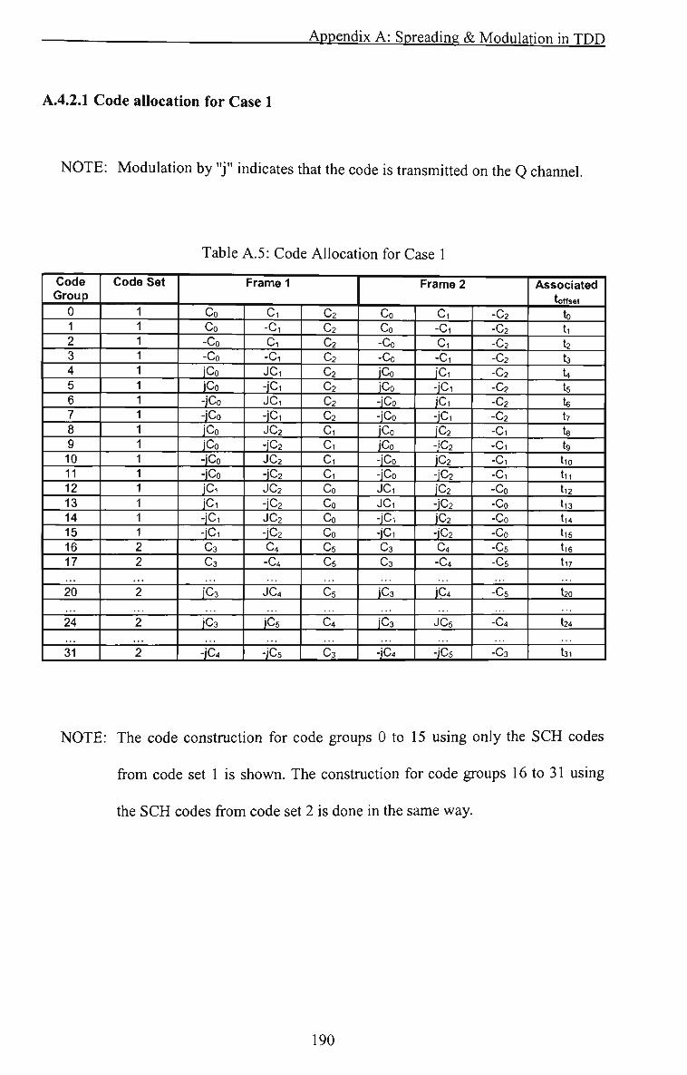
Appendix A: Spreading & Modulation in TDD
A.4.2.1 Code allocation for Case 1
NOTE: Modulation by "j" indicates that the code is fransmitted on the Q channel.
Table A,5: Code Allocation for Case 1
Code Group
0 1 2 3 4 5 6 7 8 9 10 11 12 13 14 15 16 17
20
24
31
Code Set
2 2
2
2
2
Frame 1
Co Co -Co -Co iCo jCo -iCo -jCo jCo jCo -jCo -iCo JCi jCi -jCi -iCi C3 C3
iC3
iC3
-iC4
Ci -Ci Ci -Ci JCi -jCi JC, -iCi JC2 -iC2 JC2 -iC2 JC2 -jC2 JC2 -iC2 C4 -C4
JC4
jCs
-jCs
C2 C2 C2 C2 C2 C2 C2 C2 Ci Ci Ci Ci Co Co Co Co Cs C5
Cs
C4
Ca
Frame 2
Co Co -Co -Co jCo jCo -jCo -jCo jCo jCo -iCo -iCo JCi JCi -jCi -jCi C3 C3
jC3
JC3
-JC4
Cl -Ci
Cl
-Cl
JCi -JCi JC, -iCi JC2 -jC2 JC2 -jC2 jC2 -jC2 iC2 -JC2 C4 -C4
JC4
JCs
-JCs
-C2
-C2
-C2
-C2
-C2
-C2
-C2
-C2 -Ci
-Ci
-Ci
-Ci
-Co -Co -Co -Co -Cs -Cs
-Cs
-C4
-Ca
Associated toffset
to tl
t2
ta t4 ts ts tr te ts tio tii
tl2
tl3
tl4
tl5
tl6
tl7
t20
t24
ta.
NOTE; The code constmction for code groups 0 to 15 using only the SCH codes
from code set 1 is shown. The constmction for code groups 16 to 31 using
the SCH codes from code set 2 is done in the same way.
190

Appendix A: Spreading & Modulation in TDD
A.4.2.2 Code allocation for Case 2
Table A,6: Code Allocation for Case 2
Code Group
0 1 2 3 4 5 6 7 8 9 10 11 12 13 14 15 16
23 24
31
Set
2 2 2 2 2 2 2 2 3
3 4
4
Frame 1
S l o t k
Co Co jCo jCo jCo jCo JCi JCi Ca C3 jC3 jCa JC3 JC3 jC4 jC4 Ce
jC7 Cg
jCio
Ci -Ci jCi -jCi jC2 -iC2 jC2 -jC2 C4 -C4 jC4 -iC4 jCs -jCs jCs -JCs c?
-iCs Cio
jC i i
C2 C2 C2 C2 Ci Ci Co Co Cs Cs Cs Cs C4 C4 Ca Ca Ce
Cs Ci 1
Cg
Slot k+8
Co Co jCo jCo jCo jCo JCi JCi Ca Ca jC3 JC3 jC3 iC3 iC4 iC4 Ce
iC7 Cg
jCio
Cl -Ci jCi -iCi jC2 -iC2 jC2 -jC2 C4 -C4 jC4 -iC4 jCs -jCs jCs -jCs Cz
-iCa Cio
jC i i
-C2 -C2 -C2 -C2 -Cl -Cl -Co -Co -Cs -Cs -Cs -Cs -C4 -C4 -C3 -C3 -Ce
-Ce -Cii
-Cg
Frame 2
S lo t k
-Co -Co -jCo -jCo -jCo -jCo -jCi -jCi -C3 -C3 -jC3 -jC3 -iCa -iC3 -jC4 -jC4 -Ce
-iC7 -Cg
jCio
-Ci Cl
-jCi jCi -jC2 jC2 -jC2 iC2 -C4 C4
-jC4 iC4 -jCs jCs -jCs jCs -C7
jCe -Cio
jC i i
C2 C2 C2 C2 Cl Ci Co Co Cs Cs Cs Cs C4 C4 C3 Ca Ce
Ce Ci 1
Cg
Slot k+8
-Co -Co -jCo -jCo -jCo -iCo -iCi -jCi -Ca -Ca -jCa -iCa -iC3 -iCa -jC4 -jC4 -Ce
-jC7 -Cg
jCio
-Cl Ci
-jCi jCi -jC2 jC2 -iC2 jC2 -C4 C4
-jC4 iC4 -jCs jCs -jCs iCs -C7
jCe -Cio
jC i i
-C2 -C2 -C2 -C2 -Ci -Ci -Co -Co -Cs -Cs -Cs -Cs -C4 -C4 -Ca -Ca -Ce
-Ce -Ci i
-Cg
Asso ciate
d toffset
to tl t2 ta t , ts te t7 te tg tio t i i
tl2
tia tl4
tis tie
t20
t24
tat
NOTE: The code constmction for code groups 0 to 15 using the SCH codes from
code sets 1 and 2 is shown. The constmction for code groups 16 to 31 using
the SCH codes from code sets 3 and 4 is done in the same way,
A.4.3 Evaluation of synchronisation codes
The evaluation of information fransmitted in SCH on code group and frame timing is
shown in table 6, where the 32 code groups are Usted, Each code group is containing 4
specific scrambling codes (cf subclause 6,3), each scrambUng code associated with a
specific short and long basic midamble code.
191

Appendix A: Spreading & Modulation in TDD
Each code group is additionally linked to a specific toffset, thus to a specific frame
timing. By using this scheme, the UE can derive the position ofthe frame border due to
the position ofthe SCH sequence and the knowledge of toffset- The complete mapping of
Code Group to Scrambling Code, Midamble Codes and toffset is depicted in Table A, 7.
Table A,7: Mapping scheme for Cell Parameters, Code Groups, Scrambling Codes, Midambles and toffset
CELL PARAMETER
0 1 2 3 4 5 6 7
Code Group
Group 0
Group 1
Associated Codes Scrambling
Code
CodeO Code 1 Code 2 Code 3 Code 4 Codes Code 6 Code 7
Long Basic Midamble
Code nripLo mpLi
mpL2
mpL3
mpL4
mpLs
mpLe
mpL7
Short Basic Midamble
Code msLo msLi
msL2
msL3
msL4
msLs msie msL7
Associat ed toffset
to
t l
124 125 126 127
Group 31 Code 124 Code 125 Code 126 Code 127
mpL124
inpL125
mpL126
mpL127
msL124
nrisLi2s msL126
mSL127
tai
Each cell shall cycle through two sets of cell parameters in a code group with the cell
parameters changing each frame.
Table A, 8 shows how the cell parameters are cycled according to the SFN,
192

Appendix A: Spreading & Modulation m TDD
Table A, 8: Alignment of cell parameter cycling and SFN
Initial Cell Parameter
Assignment 0 1 2 3 4 5 6 7
Code Group
Group 1
Group 2
Cell Parameter used when
SFN mod 2 = 0 0 1 2 3 4 5 6 7
Cell Parameter used when
SFN mod 2 = 1 1 0 3 2 5 4 7 6
124 125 126 127
Group 32 124 125 126 127
125 124 127 126
193

Appendix B: Comparator Noise Analvsis
Appendix B
Comparator Noise Analysis
Prior to the calculation ofthe total noise present in the dynamic comparator, lets remind
our selves about the major noise source in CMOS transistors,
B.l Noise in MOS Transistors
The two major noise sources found in CMOS transistors are thermal noise and flicker
noise. This section briefly describes these two noise sources,
B.1.1 Thermal Noise
The occurrence of thermal noise in CMOS transistors is due to the random thermal
motion of electrons since the typical electrons drift velocities in a conductor are much
less than elecfron thermal noise. This is independent of frequency and is given by:
ii" =AkT' ^^'"^ A/ (B.l) \ ^ J
where gm is the MOS fransconductance and Af is the bandwidth in Hz,
194

Appendix B: Comparator Noise Analvsis
B.1.2 Flicker Noise
The flicker noise in a transistor is caused by traps associated with contamination and
crystal defects. This noise is inversely proportional to the frequency and is given by:
i'=K-f T ''\
^ D
f ¥ (B.2)
\ J J
where ID is the drain current. A" is a constant for a particular device, Af is the bandwidth
in Hz, and a is a constant in the ranges of 0.5 -> 2. One of the most popular noise
models of MOS transistors was shown in Figure 4.7 and is used in this thesis for noise
calculations. In this model, all the noise sources from each transistor are lumped into an
equivalent input noise generator. The model is given by:
vi = ^Af + K^-^Af (B.3) ^gm f
The flicker noise component is approximately independent of bias current and voltage.
For typical MOS transistor, flicker noise is inversely proportional to the active gate area
of the fransistor, and it is also inversely proportional to the gate-oxide capacitance per
unit area. The noise generator for MOS transistor, thus, can be expressed as follows:
V'=^Af + ^-Af (B.4) ' 3g„ WLC^J
195

Appendix B: Comparator Noise Analvsis
where W and L are the width and length of a MOS transistor, respectively. Cox is tiie
oxide capacitance, gm is the MOS fransconductance, k is the Boltzman's constant, Tis
the operation temperature, and/is the operating frequency.
The noise analysis ofthe proposed comparator in Figure 3.27 will be analysed in two
sections. The first section will be the noise of the latch circuit, and the second section
will contain the noise ofthe S-R latch circuit.
B.2 Comparator Noise Analysis
B.2.1 CMOS Latch Noise Analysis
By equating all the output noise current from each transistor in Figure 3,27, the
equivalent input noise voltage can be given by:
latch
' gm, ^
Kg^J •Ko'+V,'+V,,'+
( \ ' gm, ^
gfnj •v,' +
( \ gm.
Kg^J •V
' | 4
gm 10
ygfn, •V + ' no ^
g^ l2
Kg^^ ) Kn +
(
•V ' + g^U
yg^ij in
(B,5)
The two branches of the latch circuit are identical, therefore Equation B,5 can be
simplified to:
latch 'gm,^
VgmJ .^.;.2.p^,^.2m • ^ • 3 + 2 .
' gm ^ 10
v ^ ^ i y
• V +2' ( \ ' g^u ^ Vg^J
•Ku (B-6)
196

Appendix B: Comparator Noise Analvsis
Since the thermal noise and flicker noise are independent of each, tiiey can be
considered separately. Therefore the input noise voltage of the latch cfrcuit can be
expressed by:
V, f =V +V ^ latch ' thermal ^ ' flidiST
(B.l)
B.2.1.1 Thermal Noise of Latch Circuit
The thermal noise model of each transistor is:
V' = r S-k-T
3-gm
\ Af (B,8)
Using Equation B,6 and Equation B,8, the equivalent thermal noise for the latch circuit
can be expressed as:
thermal
(B.9)
B.2.L2 Flicker Noise of Latch Circuit
One ofthe most widely used flicker noise model for each transistor is:
V^-v K, \
W-L-fC, Af
ox )
(B.IO)
197

Appendix B: Comparator Noise Analvsis
Solving Equation B,6 and Equation B,8, the equivalent flicker noise for the latch cfrcuit
can be expressed by:
flicker
2K.
WrLrC. 1 + A l + V , 1 Mn-Kn-L,' ^1 ^i„-K„-E
. V V 2 n^-K^-Lj 2 n^-K-L,,
2 ^
4/" (B.ll)
Substituting Equation B,9 and Equation B,ll into Equation B,7, the equivalent noise
generator for the latch circuit ofthe dynamic comparator could be expressed by:
(B.12)
K^rL^•C,xJ Lo' L,' 2 ^i-K-L,,' 2 n-K-L p p II J
B.2.L3 Noise Figure of Latch Circuit
The noise figure is a measure that specifies the noise performance of a certain circuit.
This measure can be defined as:
NF = Total Output Noise
That Part of Noise due to source rests tan ce = l + - lalch
A-k-T-R^Af (B.13)
By substituting Equation B.12 into Equation B,13, the noise figure ofthe latch circuit
within the comparator could be obtained. This is given by:
198
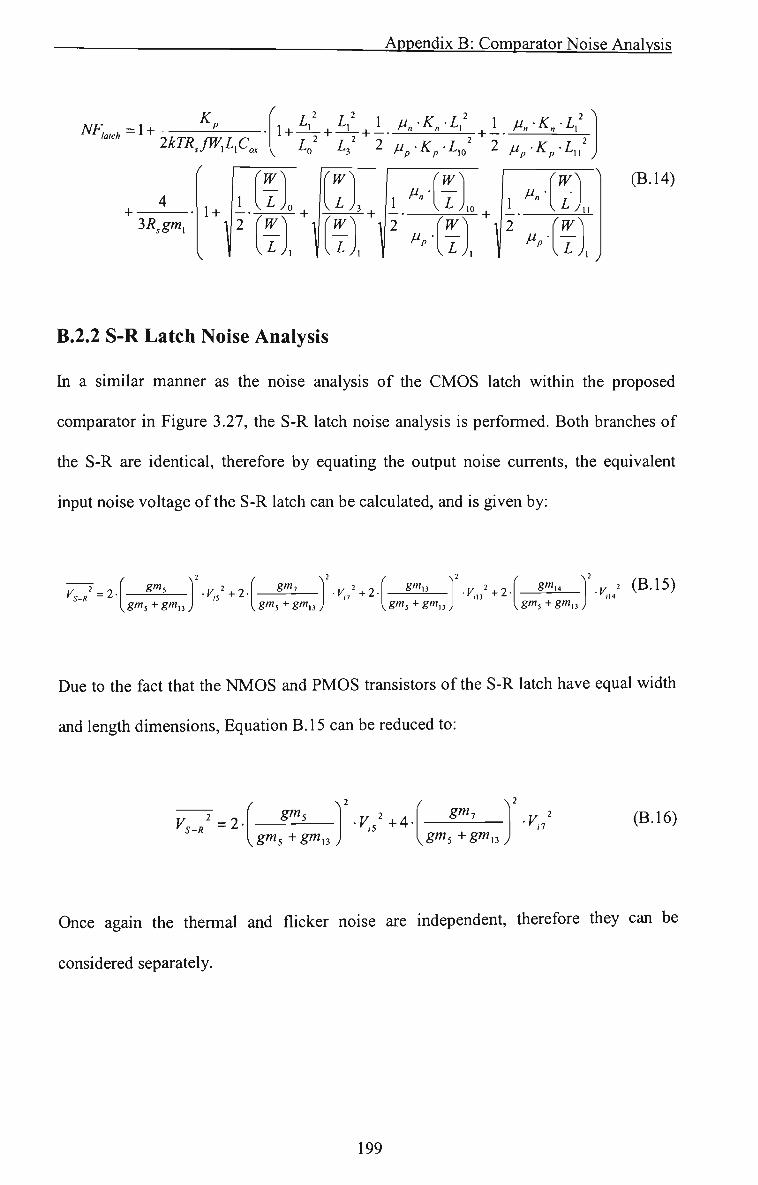
Appendix B: Comparator Noise Analvsis
NF,,tch='^ + K^
2kTR,JWAC.x f
V V 2 n^-K^-L,^ 2 n^-K^-L, 2 1 )
+ • 3R,gm^
rw^
1 ©, IS, J (W
1 ""• T . 10
2 r^^
fT
1 ^"\LJU
2 r^^
(B.14)
B.2.2 S-R Latch Noise Analysis
In a similar manner as the noise analysis of the CMOS latch within the proposed
comparator in Figure 3,27, the S-R latch noise analysis is performed. Both branches of
the S-R are identical, therefore by equating the output noise currents, the equivalent
input noise voltage ofthe S-R latch can be calculated, and is given by:
'S-R ~ 2 ' g'«5
g/«5 + g/Wij .K, /+2
gmy
{gm,+gm,j • K , / + 2 gn^y
\^
ygm,+gm,,^
( •V,/+2-
\2 .y ^ (B.15)
Due to the fact that the NMOS and PMOS transistors ofthe S-R latch have equal width
and length dimensions. Equation B.15 can be reduced to:
^ . - /=2 ' gm.
gm^+gm^^ .F,/+4.
gm,
gms+gmn V ' ''a (B.16)
Once again the thermal and flicker noise are independent, therefore they can be
considered separately.
199

Appendix B: Comparator Noise Analvsis
V =V +V ' iS ' iSUhermnl) ^ ' iS(flicVet)
( K^ \
V^5-4-Q.-/j \3-gm A/ +
(^•k-T\ ¥ (B.ll)
V. ^ =v ^ +v ^ ' i\3 '^ iU{thermal) ^'^ iUiflicker)
K. Af ^ ^ ^ '
\W,,-L,^-C,,-f) \3-gm A/ (B.18)
v-' 6"'i3y
Substituting Equation B.l7 and Equation B,18 into Equation B,16, the equivalent noise
generator for the S-R can be expressed as:
r ^.-/=4 gm.
f
{gm^+gm,^
(
f^n ?>-k-T\ • + •
-h 4 gm
V W,-L,-C,,-f 3gm Af
5 J
13
gm^+gm,^
K N
+ %-k-T\
VW,-L,,-C,,-f 3gm A/
13 y
(B.19)
The noise figure ofthe S-R latch is given by:
NF =1 + ^^ '-" A-k-T-R^-Af
(B,20)
Also equivalent to:
NF. „ = 1 + 1
S-R A-kT-R^-Af
gnis gm,+gm,.
( K, - + •
%-k-T
+ ^ ^ ^ , 3
V W^Ls-Cox-f 3-gm3
gm^+gm^j
K N • + • %-k-T\
Ws-Ln-C^x-f 3-gm,3 V " 5 -^13 ^ox
(B.21)
200

Appendix B: Comparator Noise Analvsis
The total noise figure ofthe comparator is given by:
NFc,mr>=NF,,tch-m-R = 4.48^5 (B,22)
201

Appendix C: Cadence Power Consumption Measurement ¥\o\\
Appendix C
Cadence Power Consumption Measurement Flow
Figure C, 1 illustrates the cadence power consumption measurement flow.
Design
I Simulation
Environment
— I Waveform
Viewer
£]q)ected Result
Incorrect Result
Repeat until entfre branch design is
complete
Multiplication Selection
Complete Formula of branch powers
Erase-Plot Option
Power Measurement Output
Figure C l : Cadence Power Consumption Measurement Flow
202


Related Documents


