
VT100 { Project Report
EDA385 { Computer Science { LTH
Mattias Jernberg, D06 ([email protected])Andreas Lord, D08 ([email protected])Bj�orn Uusitalo, D06 ([email protected])Supervisor: Flavius Gruian ([email protected])
November 8, 2010

Abstract
This projects implements a VT100-like serial terminal using a Nexys-2 FPGA board, VGA display, and a PS/2 keyboard. It features themost common subset of the ANSI escape codes de�ned in the ECMA-48standard, interrupt based input, serial port IO and a character-basedvideo controller. The �nal prototype is capable of running most com-mon terminal applications supporting the ECMA-48 standard, such as{ but not limited to { top, less and vim.
2

Contents
1 Introduction 1
2 System design 1
3 Protocols 2
3.1 ECMA-48 . . . . . . . . . . . . . . . . . . . . . . . . . . . . . 23.2 PS/2 . . . . . . . . . . . . . . . . . . . . . . . . . . . . . . . . 33.3 VGA . . . . . . . . . . . . . . . . . . . . . . . . . . . . . . . . 43.4 RS232 . . . . . . . . . . . . . . . . . . . . . . . . . . . . . . . 5
4 Hardware 5
4.1 VGA . . . . . . . . . . . . . . . . . . . . . . . . . . . . . . . . 54.1.1 Output generation . . . . . . . . . . . . . . . . . . . . 54.1.2 Bu�ering . . . . . . . . . . . . . . . . . . . . . . . . . 6
4.2 UART . . . . . . . . . . . . . . . . . . . . . . . . . . . . . . . 74.3 PS/2 . . . . . . . . . . . . . . . . . . . . . . . . . . . . . . . . 7
5 Software 7
6 Implementation problems 9
7 Result 9
8 Contributions 10
A Installation 11
B Downloadable resources 11
C XPS Block diagram 12
D Hardware diagrams 13
E Gallery 14
i

1 Introduction
This project aims to produce a serial terminal supporting ANSI escape codesfor formatting output and supporting a keyboard for output back to thehost device. Support is available for colourizing output, cursor placementand inserting text at any point on the screen.
The VT100 was a video terminal that was made by Digital EquipmentCorporation (DEC) in 1978. It connected to a host computer (read: main-frame) over a serial connection and allowed display of formatted text as wellas user input. The original standard for controlling the output was speci�edin ANSI X3.64, which later became ECMA-48.
The ECMA-48 is a standardization of the escape codes (usually known asANSI escape codes) which are interpreted by the terminal. The wide arrayof control codes and display modes, as well as its extensibility, has allowedit to stay relevant to this day and is enough to con�gure most embeddedequipment with a text-based serial connection.
Today most terminals are served using terminal emulation software, free-ing you from the hardware terminal and enabling use of any computer tointerface to a serially connected device. VT100 emulation can be seen as acommon factor in pretty much every such software.
2 System design
The general system design of our system is very similar to what is found ina description of a normal VT100:
� VGA output
� Keyboard input
� Serial connection
� Microcontroller
In our case however we use standard connections to all I/O instead of,like the VT100, provide them as part of the hardware. A PS/2 port providesan interface to the hardware and a HD15 VGA connector allows any VGAscreen to be connected. The microcontroller used is the Xilinx MicroBlazewhich ties together communication between the peripheral devices. Our �naldesign is shown in �gure 1. This is nearly identical with our proposal. Theshared video memory has been de�ned as being outside the VGA, whereasthe original integrated the memory inside the VGA controller. Secondly, thePmodAMP for audio beeps has been abandoned as the hardware was notavailable.
1

PLB
MicroBlaze
VGA Controller
Video RAM
Row buffer
Font ROM
Color
Pixel on/off
Color se lect
VGA out
UART PS/2PmodAMP
Copy logic
Figure 1: Architecture for the implementation
3 Protocols
As this is a system which is designed to interact with standardised periph-erals it is necessary to follow a set of protocols detailing the interactionspeci�cs of these peripherals.
3.1 ECMA-48
The ECMA-48 standard de�nes the speci�cs of terminal emulation for 7 and8 bit long characters. In addition to normal characters it de�nes controlsequences, functions, and strings that can be used to control the output tothe terminal. In this document we'll be describing the 7 bit protocol sinceit's the one we're using.
The normal way to control the output is through Control Sequences. Acontrol sequence has the following form:
CSI P...P I...I F
Where the Control Sequence Inducer (CSI) is the byte 0x5B, Parameter
2

bytes (P) are bytes between 0x30-0x3F, Intermediate bytes (I) are between0x20 and 0x2F and Final Bytes (F) are between 0x40-0x7E.
The parameter bytes encode the parameters in string of parameters instring representation. 0x30-0x39 represents the numbers 0-9, 0x3A acts asa separator between integer and decimal parts, and 0x3B separates param-eters. This maps well to the ASCII table where 0x30-0x39 maps to '0'-'9'and 0x3A, 0x3B maps to ':' and ';' respectively.
Control sequence provides a call to a control function which is speci�edby the intermediate byte and the �nal byte. The parameter bytes specifythe arguments to the function.
It's also possible to control the formatting through Independent controlfunctions and control strings. The independent control functions are mostlyaimed at controlling the device written to or the connection to the host.Control strings are prede�ned commands passed through the terminal tothe receiver without a prede�ned meaning in ECMA-48. Since neither isimplemented in our project we will not describe them in detail.
3.2 PS/2
A keyboard connecting via the PS/2 connector communicates using theprotocol devised by IBM for their PC AT computer. This protocol consistsof 8 bit commands and so called scan codes which are transferred over asynchronous serial connection.
The connector to the keyboard consists of 4 terminals, Vcc, Ground,Clock and Data. The host connector contains pull up resistors on Clock andData, keeping them normally high. The keyboard then pulls the signals tolow to send data. The keyboard clocks bits by pulling the clock low andthen releasing it making it return to a high state. First a start bit withvalue 0 is sent, followed by 8 data bits, 1 parity bit and a stop bit (a 1).
The host can also send data to the keyboard by forcing the clock to lowfor at least 60�s. This tells the keyboard to start clocking, expect a startbit and then the start of data. After the sequence of data the keyboardacknowledges by pulling the Data line low for one clock cycle.
The host to keyboard sending has priority. Thus whenever the host forcesthe clock to low to keyboard must abort or inhibit its current transmissionsto accept data from the host. To perform this safely the keyboard has asmall bu�er internally for storing key presses. This can be used to stop datafrom coming if the host cannot process any more at this time. By forcingthe clock to low and when releasing it keeping Data high (thus not sendingany start bit) the keyboard will abort the receiving of data and proceed tosend any data in its bu�er.
For an AT compatible keyboard each key has a de�ned scancode of atleast 8 bits. The scan code is sent when the key is pressed as well as on reg-ular intervals as long as the key is held down. This key repeat functionality,
3

PgUp0E7D
326
InsE070
HomeE06C
E24
R2D
Q15
W1D
636
73D
425
52E
U3C
I43
T2C
Y35
045
+4E
83E
946
Å54
¨5B
O44
P4D
´55
← 66
D23
F2B
A1C
S1B
J3B
K42
G34
H33
Ä52
'5D
L4B
Ö4C
X22
C21
<61
Z1A
N31
M3A
V2A
B32
-4A
,41
.49
⇑59
↵
5ACaps Lock
58
↹
⇑12
Ctrl14
↹0D
Alt11 29
AltGrE0 11
CtrlE0 14
F105
F206
ESC76
F503
F304
F40C
F80A
F60B
F783
F901
F1207
F1009
F1178
PgDnE07A
DelE071
EndE069
↑E075
→E074
←E06B
↓E072
21E
½0E
116
Figure 2: Scancodes on a swedish keyboard layout
called typematic, is on by default in keyboards but can be con�gured bysending commands to the keyboard. When a key is released the keyboardsends the byte F0 followed by the scan code. The scancodes and the cor-responding keys on a keyboard with Swedish layout can be seen in �gure2.
3.3 VGA
The VGA output signal is very simple; it consists of three analogue channels,one for each colour red, green and blue. In addition to these there are twosignals named vertical sync (Vsync) and horizontal sync (Hsync). These areused to tell the monitor when a new line or page is to be started.
The signal is based on how CRT monitors work. A cathode ray is guidedusing an electrical �eld which makes it sweep across the screen. As the hori-zontal voltage increases in this �eld the ray sweeps across the line outputtingthe colour which is currently put on the inputs. Hsync serves to dischargeto component supplying voltage to the electrical �eld. This is the amount oftime that Hsync is active. On a CRT there is also a part of the screen thatis hidden by the casing. To keep image stability there are two areas, one atthe beginning and one at the end named front and back porch respectivelywhich do not contain data.
All this also applies to vertical order as well, with Vsync instead ofHsync and a di�erent timing. Modern LCDs instead incorporate a chip
4
Fro
nt p
orch
Ba
ck po
rchH
sync
Figure 3: VGA scan to draw lines
which detects this timing and syncs with the incoming signal to converteach pixel to a pixel on the LCD panel.
3.4 RS232
For serial communication the RS232 protocol is used. It is an asynchronousprotocol and needs that both sides have previously agreed on a set data rateto properly communicate (since clock speeds are otherwise out of sync). Theactual serial transfer protocol is not relevant for the implementation and ishandled by a readily available chip. Thus it is not described further here.
4 Hardware
4.1 VGA
The VGA controller is the only core that was custom created. It implementsa 640x480 VGA signal at 60 Hz using a pre-made VHDL module availablefrom Digilent[4]. To generate characters from text a ROM is used to storea font with characters 8x16 pixels wide. Each character is represented inthis ROM using 16 bytes, one for each row of the character. Each bit thenrepresents the column. The output is done by two components, a pixelgenerator and a copying module lifting data from the shared video memory.Simpli�ed diagrams of these are available in appendix D.
4.1.1 Output generation
Since the counters operate on pixel positions it is necessary to translate thisinto two parts, the position of the current character and then the pixel inthat character which must be drawn. As the characters have both a widthand height as a power of 2, this is easily done by using the least signi�cant
5

Output bit Source bit(s)
Red 0 0Red 1 redRed 2 red & hi
Green 0 0Green 1 greenGreen 2 green & hiBlue 0 blueBlue 1 blue & hi
Table 1: Output colour conversion
bits as the pixel in the character and the rest of the bits as a position tellingus which character position in the frame to use.
This makes the pipeline quite straight forward. A memory is used tostore 16-bit words describing which characters to draw. This is split incolour and character number. The character value and row number is fedinto the font ROM and from this the output pixel is selected using thecurrent column.
The pixel value selects if either background or foreground colour is to beused, if reverse is on this is inverted so that foreground is background andvice versa and �nally a component tests if the current position is equal tothe set cursor position which inverts the choice once again.
The output of the VGA signal on the board is 8 bits and capable of gen-erating 256 colours. However as part of the standard we only need 7 colours(and high intensity for the foreground colour) which halves the necessarybits for storing colour values. To convert these colours with 1 bit for eachcolour to 8 bits, some trial and error resulted in the conversion shown intable 1.
A simpli�ed illustration of this pipeline can be seen in �gure 8. Inthis �gure, the output conversion as well as reversal of the colour has beenremoved to improve readability.
4.1.2 Bu�ering
When drawing to the screen, characters are drawn one pixel row at the timeand all characters on that row are drawn before the next row of pixels arebegun (as illustrated in �gure 4). If the software changes the contents ofthe memory often this can lead to strange output on the screen while done.To prevent this, a bu�ering mechanism is needed. The two choices arethe simple full bu�ering, which doubles the memory requirements, or rowbu�ering, which is the minimum amount that can be bu�ered to avoid thisproblem. This design uses a row bu�ering model since the choice at design
6
time was to preserve memory in order to avoid the need for a redesign latein the project should it be shown that there were an insu�cient amountof BRAMs in the FPGA. This result in a more complex set of states thatneeds to track both Vsync, Hsync, addresses to both bu�ers and when thereis an output signal (as there are multiple Hsync signals when we are notoutputting data on the top of the screen). This design is show in �gure 7.
Figure 4: Drawing order forpixels on the display
The general design of this copy logic is adirect copying of the current row from theshared RAM into the row bu�er. This isdriven by two counters, one for addressingeach of the memories. Since the main mem-ory is 32 bits wide a multiplexer is usedto divide this into 16 bit words which thehardware works with. The main memorycounter can be initialised to either address 0which contains 4 8-bit registers that controlthe hardware, currently they de�ne whichrow that is used as row 0 and the row andcolumn for the current cursor position.
The state machine initialises on Vsync and starts by loading address 0 inthe main counter to load the registers. It then loads the start row and waitsfor Hsync. Hsync indicates that a new set of 80 words should be loadedinto the bu�er. Afterwards it blocks until it detects an output signal to thescreen and returns to idle mode waiting for either Hsync or Vsync.
4.2 UART
For serial communication a 16550-compatible UART is used. This was cho-sen because its known features giving access to mainly FIFOs but also hand-shaking and ow control signals immediately in hardware. The latter fea-tures was shown not usable however, as the board does not connect thesepins to the FPGA. The UART in this project is provided by Xilinx andconnects to the MicroBlaze via the PLB-bus.[9]
4.3 PS/2
The PS/2 interface is provided by a pre-made core from Xilinx which con-nects to the PLB bus.[6]
5 Software
The software was written in C and can be split into three major parts.Initialisation, interrupts and the ECMA parsing which can be seen in �gure5.
7
The initialization sets up the hardware, and prints a welcome screen.The interrupts are triggered whenever the PS/2 keyboard sends a scancode.These are then decoded, keeping track of special characters and a few states,such as caps lock. Once decoded the corresponding commands or charactersare sent to the host over the serial port.
The ECMA routine decodes the response of the host and updates thescreen output accordingly. As seen in �gure 5 we handle three di�erent kindsof input: normal characters, special characters and escape codes.
Normal characters are just printed at the correct position on the screen.Special characters such as newline and backspace are interpreted correctly,for example 'nn' will cause the software to clear the next row, scroll thescreen if necessary and put the cursor at the �rst position of that row.
An escape sequence is more complex, the sequence may have a numberof parameters strings and/or a number of intermediary bytes before it endswith a �nal byte. In practice the escape sequence is a lot more complex thanneeded, no applications tested use intermediate bytes and the parametersonly contains integers. This allows us to implement a simpli�ed parsing ofescape sequences handling a �xed number of integer parameters. For debug-ging reasons a single intermediate byte is interpreted and stored, howeverno function makes use of this.
serial_getchar()
specialcharacter?
escapecode? read sequence
put VGA
PS/2 interrupt
Interpretsingle character Interpret
Update state
lookup serial_putchar()
Yes
No No
Yes
InitializeHardware
Figure 5: Drawing order for pixels on the display
8

6 Implementation problems
Design-wise our largest problem was is that we were too careful. Our designdecisions were to forego a full double bu�er of the video memory to avoidhaving to go o�-chip for more memory. To further limit memory consump-tion we limited ourselves to 2 bytes per character and removed features suchas blinking and underlined text for this reason. Given the current mem-ory usage, 3 bytes would allow for more formatting and result in a minimalincrease in device utilisation.
During the implementations we ran into a few hardware problems, wherea slow point in the execution causes hardware bu�ers to over ow. This wasparticularly visible in the PS/2 controller as the Xilinx PS/2 core does notimplement the ow control described in section 3.2 and only bu�ers a singlebyte. The biggest culprit causing these problems were the debugging asprinting to the JTAG terminal (provided by the MicroBlaze debug module)could sometimes take seconds to transfer the text. We did not �nd a goodsolution to this since no part of our input hardware were able to do owcontrol and thus only could over ow.
The Xilinx Platform Studio also provided its fair share of grief whenmigrating an ISE project into XPS as an IP core. When creating a customcore as we did using netlists from the Xilinx LogiCORE wizard intermixedwith VHDL and on top of that connecting it to a bus interface that is notcreatable using the peripheral creation wizard in XPS one have to consultthe reference manual for the �les describing peripherals[8]. This format isextremely versatile, and allows for the reuse of modules from other cores.Thus if a copy is made of a core it does, by default, use the hardware designfrom the old core without warnings. Also, while there is a version numberassociated with each core, XPS does not allow you to easily replace a corewith a newer version, even if their connections match exactly. This lead towhat was expected to take 2-3 hours for integration, took a whole day ofwork. Therefore a work ow doing design in XPS, exporting to ISE to buildthe cores and then updating the software using the SDK would be a morestreamlined method if possible. Any completed cores could then as a laststep be ported into XPS.
7 Result
The �nished prototype works well and has been tested with major softwaresuch as ncurses, vim, zshell as well as standalone hardware that utilisesescape codes to format a user interface. Currently only a single known issueexists, however its cause is unknown. The bug does not crash the devicebut merely garbles the output until a clear or similar redraw of the screen isperformed. The �nal device utilisation is shown in table 2. The software is
9
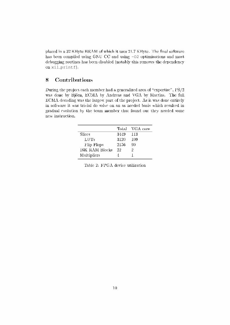
placed in a 32 KByte BRAM of which it uses 21:7 KByte. The �nal softwarehas been compiled using GNU CC and using -O2 optimisations and mostdebugging routines has been disabled (notably this removes the dependencyon xil printf).
8 Contributions
During the project each member had a generalized area of \expertise", PS/2was done by Bj�orn, ECMA by Andreas and VGA by Mattias. The fullECMA decoding was the largest part of the project. As it was done entirelyin software it was trivial do solve on an as needed basis which resulted ingradual evolution by the team member that found out they needed somenew instruction.
Total VGA core
Slices 3449 113LUTs 3120 109Flip Flops 2156 90
16K RAM Blocks 22 2Multipliers 4 1
Table 2: FPGA device utilization
10

A Installation
Using a Nexys2-1200 board, connect a VGA display, a PS/2 keyboard andyour serial device to the board. Make sure the device you are using is nottransmitting on the serial port (if possible, turn it o�).
Using a Nexys2-1200 FPGA board, download the bit �le to your board.Use vt100_CCLK.bit for programming the PROM and vt100_JTAGCLK.bitfor downloading directly to the FPGA chip. If programming the PROM,power cycle the board after completion. You will now see an instructionscreen helping you get started. The baud rate is con�gurable using theswitches on the board; each switch is mapped to a unique speed. No switchesenabled mean 1200 baud and then each switch is mapped in order to 2400,4800, 9600, 19200, 38400, 57600, 115200, 230400 baud. If multiple baudrates are selected the highest will be used. As you select a baud rate it willbe presented to you on the screen if you are unsure. Be advised that selecting230400 baud has not been proven safe and might lead to unexpected lockups.
When satis�ed, start your device using the same baud rate. The baudrate will now be locked for the rest of the session (you must press BTN0 toreset the board and tell it to load a new setting).
B Downloadable resources
http://users.student.lth.se/˜dt06mj4/vt100/vt100_CCLK.bithttp://users.student.lth.se/˜dt06mj4/vt100/vt100_JTAGCLK.bit
Bit �les for programming the Nexys2-board, see also appendix A.
http://users.student.lth.se/˜dt06mj4/vt100/report.zipReport source, with sources for graphics used. Permission granted to use
and modify these �les under CC-by-SA 3.0.
http://users.student.lth.se/˜dt06mj4/vt100/vt100.zipXilinx Platform Studio hardware project and external tools. The direc-
tory structure is as follows:
fpga/master The main Xilinx Platform Studio project
fpga/master/VT100 C code running on the MicroBlaze
fpga/vga ise Development project for the VGA hardware using XilinxISE
support/vgafont Converter tools for PSF1 font �les (Linux console fonts)
11
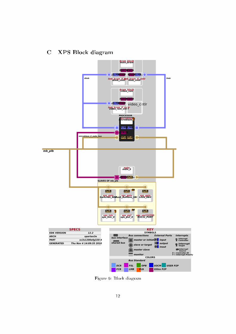
C XPS Block diagram
bram_blockmain_bram
PORTAPORTB
lmb_bram_if_cntlrdlmb_cntlr
SLMBBRAM
lmb_bram_if_cntlrilmb_cntlr
SLMBBRAM
bram_blockvideo_ram
PORTAPORTB
lmb_bram_if_cntlrvideo_ram_cntrl
SLMBBRAM
mdmmdm_0
SPLBMBDE
xps_gpioSwitches_8Bit
SPLB
xps_gpioPush_Buttons_3Bit
SPLB 00
xps_gpioLEDs_8Bit
SPLB
xps_intcxps_intc_0
SPLB 0
xps_ps2xps_ps2_0
SPLB 10
xps_uart16550RS232_PORT
SPLB
SLAVES OF mb_plb
microblazemicroblaze_0
DLMBILMB
DPLBIPLB
DEBUG
0
PROCESSOR
dlmb
microblaze_0_mdm_bus
ilmb
mb_plb
KEYSYMBOLS
bus interface
shared bus
Bus connections
master or initiator
slave or target
master slave
monitor
External Ports
input
output
inout
Interrupts
xInterruptController
xInterruptTarget
yxInterruptSource
X = Controller IDY = Interrupt Priority
COLORSBus Standard
DCR
FCB
FSL
LMB
OPB
PLB
SOCM
Xilinx P2P
USER P2P
SPECSEDK VERSION 12.2
ARCH spartan3e
PART xc3s1200efg320-4
GENERATED Thu Nov 4 14:09:35 2010
video_cntlr
Figure 6: Block diagram
12

D Hardware diagrams
11
16
78
16
11
1610
8
11
D
enableload
value
Counter
31:2423:1615:87:0
AD
we
Row buffer memory31:1615:0
VGA_MEM_START: 0x2
01
80
in2
in1
eq==
Main memory
10:10
EQ
D
REG_ADDR: 0x0
CE
valuecounter
1 0
OE
vsync
hsyncto_registers
read_registers
copy
to_top
State_Machine
A D
20
Figure 7: VGA row bu�ering component
3
7
7
3
11
4
16
104
8
4
9:43:0
9:32:0
14:87:43:0
A DA D
76543210
QD
01
07
FONT ROM
10:76:0
Row buffer
column row
vsync
hsync
VgaCtrl640_60
Outputcolor
Figure 8: VGA output component
13
E Gallery
14

References
[1] Digilent Inc. Digilent Plug-in for Xilinx 12.x Tools User Man-
ual. http://fileadmin.cs.lth.se/cs/Education/EDA385/HT10/documents/chipscope_digilent/Digilent_Plug-in_Xilinx_v12.pdf.
[2] ECMA. ECMA-48: Control Functions for Coded Character Sets. ECMA(European Association for Standardizing Information and Communica-tion Systems), pub-ECMA:adr, �fth edition, June 1991.
[3] Digilent Inc. Master ucf �le for the nexys2-1200. http://www.digilentinc.com/Data/Products/NEXYS2/Nexys2_1200General.zip.
[4] Digilent Inc. Vga controller reference design. http://www.digilentinc.com/Data/Documents/Reference%20Designs/VGA%20RefComp.zip.
[5] The Linux man-page project. console codes(4).
[6] Xilinx. LogiCORE IP XPS PS2 Controller (v1.01b), april 2010. DS707.
[7] Xilinx. MicroBlaze Processor Reference Guide, jul 2010. UG081 v11.1.
[8] Xilinx. Platform Speci�cation Format Reference Manual (EDK 12.2),jul 2010. UG642.
[9] Xilinx. XPS 16550 UART (v3.00a), may 2010. DS577.
15


