ORDER NO. PIONEER CORPORATION 4-1, Meguro 1-chome, Meguro-ku, Tokyo 153-8654, Japan PIONEER ELECTRONICS (USA) INC. P.O. Box 1760, Long Beach, CA 90801-1760, U.S.A. PIONEER EUROPE NV Haven 1087, Keetberglaan 1, 9120 Melsele, Belgium PIONEER ELECTRONICS ASIACENTRE PTE. LTD. 253 Alexandra Road, #04-01, Singapore 159936 PIONEER CORPORATION 2002 N∫m-Û.,, VSX-D511 RRV2581 AUDIO/VIDEO MULTI-CHANNEL RECEIVER VSX-D511 THIS MANUAL IS APPLICABLE TO THE FOLLOWING MODEL(S) AND TYPE(S). Model Type Power Requirement Remarks VSX-D511 KUXJI AC120V VSX-D511 KCXJI AC120V For details, refer to "Important symbols for good services" on the next page. T-ZZR FEB.2002.printed in Japan

Welcome message from author
This document is posted to help you gain knowledge. Please leave a comment to let me know what you think about it! Share it to your friends and learn new things together.
Transcript

PIONEER CORPORATION 4-1, Meguro 1-chome,PIONEER ELECTRONICS (USA) INC. P.O. Box 1760, LonPIONEER EUROPE NV Haven 1087, Keetberglaan 1, 912PIONEER ELECTRONICS ASIACENTRE PTE. LTD. 253
PIONEER CORPORATION 2002
DOWN
STATION
TUNER EDIT INPUT ATT FL DIMMERCLASS BAND MPX
STANDARDADVANCEDSURROUND
STEREO/DIRECT
SIGNALSELECT
UP
ENTER
INPUTSELECTOR
MASTER VOLUME
MULTI JOG
AUDIO/VIDEO MULTI-CHANNEL RECEIVER
R
STANDBY
STANDBY/ON
PHONES
TUNING MONITOR
MULTI JOG
MULTI JOG
MIDNIGHT LOUDNESS TONE QUICK SETUP
LISTENING MODE
N∫m-Û.,,
VSX-D511
Meguro-ku, Tokyo 153-8654, Japang Beach, CA 90801-1760, U.S.A.
0 Melsele, BelgiumAlexandra Road, #04-01, Singapore 159936
ORDER NO.
RRV2581
AUDIO/VIDEO MULTI-CHANNEL RECEIVER
VSX-D511THIS MANUAL IS APPLICABLE TO THE FOLLOWING MODEL(S) AND TYPE(S).
Model Type Power Requirement Remarks
VSX-D511 KUXJI AC120V
VSX-D511 KCXJI AC120V
For details, refer to "Important symbols for good services" on the next page.
T-ZZR FEB.2002.printed in Japan

A
B
C
D
1 2 3 4
VSX-D5112
SAFTY INFORMATION
This service manual is intended for qualified service technicians ; it is not meant for the casual do-it-yourselfer. Qualified technicians have the necessary test equipment and tools, and have been trainedto properly and safely repair complex products such as those covered by this manual.Improperly performed repairs can adversely affect the safety and reliability of the product and mayvoid the warranty. If you are not qualified to perform the repair of this product properly and safely, youshould not risk trying to do so and refer the repair to a qualified service technician.
WARNINGThis product contains lead in solder and certain electrical parts contain chemicals which are known to the state of California to causecancer, birth defects or other reproductive harm.
Health & Safety Code Section 25249.6 – Proposition 65
NOTICE(FOR CANADIAN MODEL ONLY)Fuse symbols (fast operating fuse) and/or (slow operating fuse) on PCB indicate that replacement parts mustbe of identical designation.
REMARQUE(POUR MODÈLE CANADIEN SEULEMENT)Les symboles de fusible (fusible de type rapide) et/ou (fusible de type lent) sur CCI indiquent que les piècesde remplacement doivent avoir la même désignation.
ANY MEASUREMENTS NOT WITHIN THE LIMITSOUTLINED ABOVE ARE INDICATIVE OF A POTENTIALSHOCK HAZARD AND MUST BE CORRECTED BEFORERETURNING THE APPLIANCE TO THE CUSTOMER.
2. PRODUCT SAFETY NOTICE Many electrical and mechanical parts in the appliancehave special safety related characteristics. These areoften not evident from visual inspection nor the protectionafforded by them necessarily can be obtained by usingreplacement components rated for voltage, wattage, etc.Replacement parts which have these special safetycharacteristics are identified in this Service Manual. Electrical components having such features are identifiedby marking with a on the schematics and on the parts listin this Service Manual.The use of a substitute replacement component which doesnot have the same safety characteristics as the PIONEERrecommended replacement one, shown in the parts list inthis Service Manual, may create shock, fire, or other hazards. Product Safety is continuously under review and newinstructions are issued from time to time. For the latestinformation, always consult the current PIONEER ServiceManual. A subscription to, or additional copies of, PIONEERService Manual may be obtained at a nominal charge fromPIONEER.
1. SAFETY PRECAUTIONS The following check should be performed for thecontinued protection of the customer and servicetechnician.
LEAKAGE CURRENT CHECK Measure leakage current to a known earth ground (waterpipe, conduit, etc.) by connecting a leakage current testersuch as Simpson Model 229-2 or equivalent between theearth ground and all exposed metal parts of the appliance(input/output terminals, screwheads, metal overlays, controlshaft, etc.). Plug the AC line cord of the appliance directlyinto a 120V AC 60Hz outlet and turn the AC power switchon. Any current measured must not exceed 0.5mA.
(FOR USA MODEL ONLY)
Leakagecurrenttester
Reading shouldnot be above0.5mADevice
undertest
Test allexposed metalsurfaces
Also test withplug reversed(Using AC adapterplug as required)
Earthground
AC Leakage Test
1 2 3 4
A
B
C
D
5 6 7 8
VSX-D511
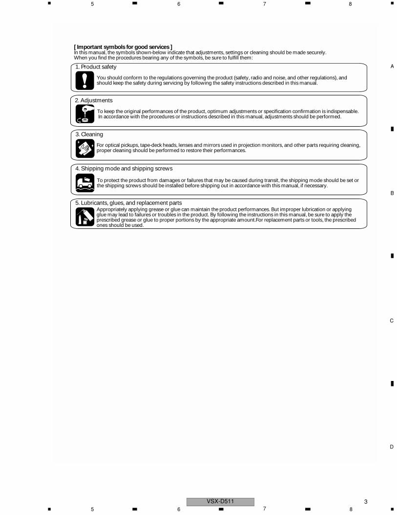
[ Important symbols for good services ]In this manual, the symbols shown-below indicate that adjustments, settings or cleaning should be made securely.When you find the procedures bearing any of the symbols, be sure to fulfill them:
2. Adjustments
To keep the original performances of the product, optimum adjustments or specification confirmation is indispensable. In accordance with the procedures or instructions described in this manual, adjustments should be performed.
3. Cleaning
For optical pickups, tape-deck heads, lenses and mirrors used in projection monitors, and other parts requiring cleaning,proper cleaning should be performed to restore their performances.
5. Lubricants, glues, and replacement partsAppropriately applying grease or glue can maintain the product performances. But improper lubrication or applying glue may lead to failures or troubles in the product. By following the instructions in this manual, be sure to apply theprescribed grease or glue to proper portions by the appropriate amount.For replacement parts or tools, the prescribed ones should be used.
4. Shipping mode and shipping screws
To protect the product from damages or failures that may be caused during transit, the shipping mode should be set orthe shipping screws should be installed before shipping out in accordance with this manual, if necessary.
1. Product safety
You should conform to the regulations governing the product (safety, radio and noise, and other regulations), and should keep the safety during servicing by following the safety instructions described in this manual.
5 6 7 83

A
B
C
D
1 2 3 4
VSX-D5114
CONTENTS SAFTY INFORMATION . . . . . . . . . . . . . . . . . . . . . . . . . . . . . . . . . . . . . . . . . . . . . 2
1. SPECIFICATIONS . . . . . . . . . . . . . . . . . . . . . . . . . . . . . . . . . . . . . . . . . . . . . . . 5
2. EXPLODED VIEWS AND PARTS LIST . . . . . . . . . . . . . . . . . . . . . . . . . . . . . . . . . . . . 6
2.1 PACKING . . . . . . . . . . . . . . . . . . . . . . . . . . . . . . . . . . . . . . . . . . . . . . . . . 6
2.2 EXTERIOR SECTION . . . . . . . . . . . . . . . . . . . . . . . . . . . . . . . . . . . . . . . . . . . 8
2.3 FRONT PANEL SECTION . . . . . . . . . . . . . . . . . . . . . . . . . . . . . . . . . . . . . . . . 10
3. BLOCK DIAGRAM AND SCHEMATIC DIAGRAM . . . . . . . . . . . . . . . . . . . . . . . . . . . . . . 12
3.1 BLOCK DIAGRAM . . . . . . . . . . . . . . . . . . . . . . . . . . . . . . . . . . . . . . . . . . . . 12
3.2 OVERALL WIRING CONNECTION DIAGRAM . . . . . . . . . . . . . . . . . . . . . . . . . . . . . 14
3.3 D.D & INPUT(1/4) ASSY. . . . . . . . . . . . . . . . . . . . . . . . . . . . . . . . . . . . . . . . . 16
3.4 D.D & INPUT(2/4) ASSY. . . . . . . . . . . . . . . . . . . . . . . . . . . . . . . . . . . . . . . . . 18
3.5 D.D & INPUT(3/4) ASSY. . . . . . . . . . . . . . . . . . . . . . . . . . . . . . . . . . . . . . . . . 20
3.6 D.D & INPUT(4/4) ASSY. . . . . . . . . . . . . . . . . . . . . . . . . . . . . . . . . . . . . . . . . 22
3.7 AMP & PRIMARY(1/2), TRANS2 and TRANS3 ASSYS . . . . . . . . . . . . . . . . . . . . . . . . . 24
3.8 AMP & PRIMARY(2/2), REGULATOR, AMP INPUT and TRANS1 ASSYS . . . . . . . . . . . . . . . 26
3.9 VIDEO, 6CH IN and S.VIDEO ASSYS. . . . . . . . . . . . . . . . . . . . . . . . . . . . . . . . . . 28
3.10 FRONT, R.ENCODER and POWER SW ASSYS . . . . . . . . . . . . . . . . . . . . . . . . . . . 30
3.11 DIGITAL IN, H.P. and KAWA ASSYS . . . . . . . . . . . . . . . . . . . . . . . . . . . . . . . . . . 32
3.12 FM/AM TUNER MODULE . . . . . . . . . . . . . . . . . . . . . . . . . . . . . . . . . . . . . . . 34
4. PCB CONNECTION DIAGRAM . . . . . . . . . . . . . . . . . . . . . . . . . . . . . . . . . . . . . . . 36
4.1 TRANS1, TRANS2 and TRANS3 ASSYS . . . . . . . . . . . . . . . . . . . . . . . . . . . . . . . . 37
4.2 D.D & INPUT ASSY . . . . . . . . . . . . . . . . . . . . . . . . . . . . . . . . . . . . . . . . . . . 38
4.3 AMP INPUT and AMP ASSYS. . . . . . . . . . . . . . . . . . . . . . . . . . . . . . . . . . . . . . 42
4.4 FRONT, POWER SW, H.P. and R.ENCODER ASSYS . . . . . . . . . . . . . . . . . . . . . . . . . 44
4.5 REGULATOR, HASHIGETA and KAWA ASSYS. . . . . . . . . . . . . . . . . . . . . . . . . . . . . 48
4.6 DIGITAL IN, 6CH IN, VIDEO and BOARD TO BOARD ASSYS . . . . . . . . . . . . . . . . . . . . . 50
4.7 FM/AM TUNER MODULE . . . . . . . . . . . . . . . . . . . . . . . . . . . . . . . . . . . . . . . . 52
5. PCB PARTS LIST . . . . . . . . . . . . . . . . . . . . . . . . . . . . . . . . . . . . . . . . . . . . . . 53
6. ADJUSTMENT . . . . . . . . . . . . . . . . . . . . . . . . . . . . . . . . . . . . . . . . . . . . . . . . 58
7. GENERAL INFORMATION. . . . . . . . . . . . . . . . . . . . . . . . . . . . . . . . . . . . . . . . . . 59
7.1 DISASSEMBLY and DIAGNOSI . . . . . . . . . . . . . . . . . . . . . . . . . . . . . . . . . . . . . 59
7.2 PARTS . . . . . . . . . . . . . . . . . . . . . . . . . . . . . . . . . . . . . . . . . . . . . . . . . . 64
7.2.1 IC . . . . . . . . . . . . . . . . . . . . . . . . . . . . . . . . . . . . . . . . . . . . . . . . . . . 64
7.2.2 DISPLAY . . . . . . . . . . . . . . . . . . . . . . . . . . . . . . . . . . . . . . . . . . . . . . . . 73
8. PANEL FACILITIES . . . . . . . . . . . . . . . . . . . . . . . . . . . . . . . . . . . . . . . . . . . . . 75
1 2 3 4

A
B
C
D
5 6 7 8
VSX-D511
1. SPECIFICATIONS
Î
Accessories
Remote control unit(XXD3038)
AM loop antenna(ATB7009)
FM wire antenna(ADH7004)
AA size IEC R6PDry cell batteries (x2)
Amplifier SectionContinuous average power output of 100 watts* per channel, min.,at 8 ohms, from 20 Hz to 20,000 Hz with no more than 0.2 %** totalharmonic distortion (front).
Continuous Power OutputFront .................................... 100 W per channel (1kHz, 1.0 %, 8 Ω)Center ..................................................... 100 W (1kHz, 1.0 %, 8 Ω)Surround .............................. 100 W per channel (1kHz, 1.0 %, 8 Ω)Surround Back .................... 100 W per channel (1kHz, 1.0 %, 8 Ω)
Input (Sensitivity/Impedance)CD, VCR/DVR, CD-R/TAPE/MD, DVD/LD, TV/SAT ... 200 mV/47 kΩ
Frequency ResponseCD, VCR/DVR, CD-R/TAPE/MD, DVD/LD,TV/SAT.................................................................. 5 Hz to 100,000 Hz dB
Output (Level/Impedance)VCR/DVR REC, CD-R/TAPE/MD REC .................... 200 mV/2.2 kΩ
Tone ControlBASS ...................................................................... ± 6 dB (100 Hz)TREBLE .................................................................. ± 6 dB (10 kHz)LOUDNESS ..................................... +9 dB/+9 dB (100 Hz/10 kHz)
Signal-to-Noise Ratio (IHF, short circuited, A network)CD, VCR/DVR, CD-R/TAPE/MD,DVD/LD, TV/SAT .................. 96 dB
Signal-to Noise Ratio [EIA, at 1 W (1 kHz)]CD, VCR/DVR, CD-R/TAPE/MD,DVD/LD, TV/SAT .................. 79 dB
Video Section
Input (Sensitivity/Impedance)VCR/DVR, DVD/LD, TV/SAT ......................................... 1 Vp-p/75 Ω
Output (Level/Impedance)VCR/DVR ...................................................................... 1 Vp-p/75 Ω
Frequency ResponseVCR/DVR, DVD/LD,TV/SAT ] MONITOR ........ 5 Hz to 7 MHz dBSignal-to-Noise Ratio .............................................................. 55 dBCross Talk ............................................................................... 55 dB
FM Tuner SectionFrequency Range .......................................... 87.5 MHz to 108 MHzUsable Sensitivity .......................Mono:13.2 dBf, IHF (1.3 µV/ 75 Ω)50 dB Quieting Sensitivity ......................................... Mono: 20.2 dB
Stereo: 38.6 dBfSignal-to-Noise Ratio ................................. Mono: 73 dB (at 85 dBf)
Stereo: 70 dB (at 85 dBf)Distortion ........................................................ Stereo: 0.5 % (1 kHz)Alternate Channel Selectivity ................................. 60 dB (400 kHz)Stereo Separation ...................................................... 40 dB (1 kHz)Frequency Response ................................. 30 Hz to 15 kHz (±1 dB)Antenna Input (DIN) .............................................. 75 Ω unbalanced
AM Tuner SectionFrequency Range ........................................... 530 kHz to 1,700 kHzSensitivity (IHF, Loop antenna) ......................................... 350 µV/mSelectivity ................................................................................ 25 dBSignal-to-Noise Ratio .............................................................. 50 dBAntenna ...................................................................... Loop antenna
MiscellaneousPower Requirements ............................................... AC 120 V, 60HzPower Consumption
VSX-D511 ...........................................................
...........................................................
260W (KU)
340VA (KC)
In Standby ............................................................................. 1 WAC Outlet ................................................ 100 W MAX. (SWITCHED)Dimensions ................................... 420 (W) x 158 (H) x 393 (D) mm
(16-9/16 (W) x 6-4/16 (H) x 15-8/16 (D) in.)Weight (without package)
kgVSX-D511 .......................................................................... 9.0 (19.8 lb)
Furnished PartsAM loop antenna ............................................................................ 1FM wire antenna ............................................................................ 1Dry cell batteries (AA size IEC R6P) .............................................. 2Remote control ............................................................................... 1Operating instructions .................................................................... 1
Specifications and the design are subject to possible modificationswithout notice, due to improvements.
* Measured pursuant to the Federal Trade Commission’s TradeRegulation rule on Power Output Claims for Amplifiers.
** Measured by Audio Spectrum Analyzer.
+0– 3
+0– 3
"DTS" ,“ES” and "DTS Digital Surround" are trademarks
of Digital Theater Systems, Inc.
Manufactured under license from Dolby Laboratories.
“Dolby”, “Pro Logic II” and the double D symbol 2 are
trademarks of Dolby Laboratorories.
INP
UT
SE
LEC
TOR CD
TV/S
ATD
VD
/LD
RECE
IVER
DV
D
DV
D C
ON
TRO
L
SUB
TITL
E
AU
DIO
TES
TTO
NE
LEV
EL
EFF
EC
T
ME
NU
DVD
TUN
ERED
IT
RECE
I-VE
R
TOP
ME
NU
STAN
DARD
STER
EOAD
VANC
EDSU
RROU
ND
INPU
TAT
TFL
DIM
MER
MUT
E
MA
STER
VOLU
ME
CD
-R/
TAP
E/M
DV
CR
/D
VR
ENTE
R
SETU
P
AV R
EC
EIV
ER
TUN
ING
BAN
DC
LASS
MPX
DISP
LAY
CH SE
LECT
STAT
ION
MIDN
IGHT
/LO
UDNE
SSTU
NE
R
1
¢4
¡
78
3
5 6 7 85
A
B
C
D
1 2 3 4
VSX-D5116
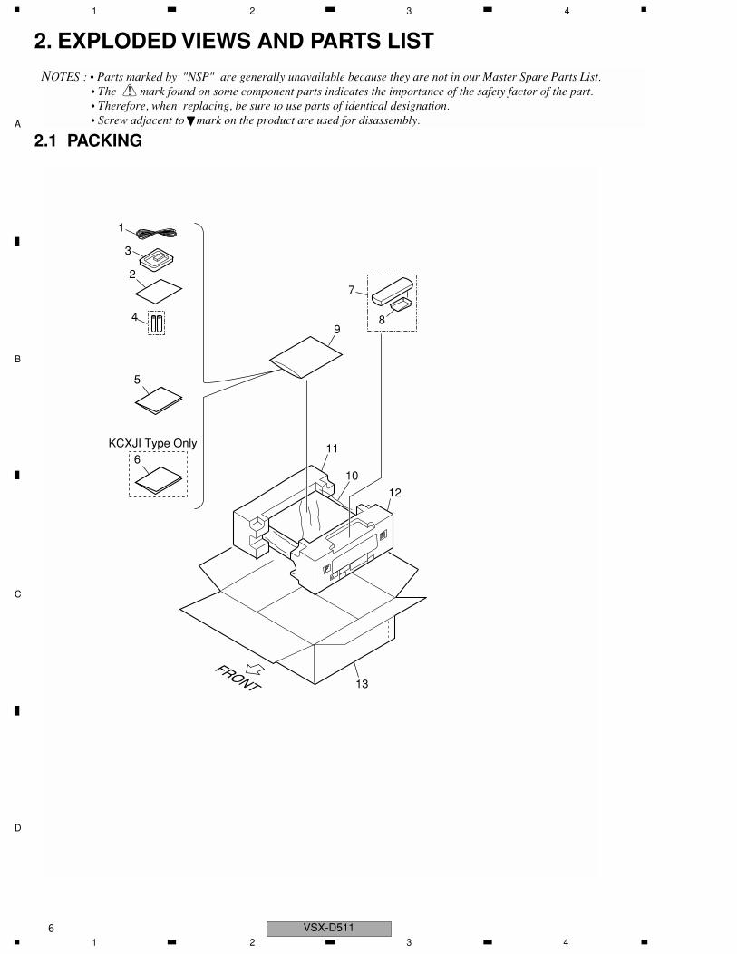
2. EXPLODED VIEWS AND PARTS LIST
2.1 PACKING
NOTES : • Parts marked by "NSP" are generally unavailable because they are not in our Master Spare Parts List. • The > mark found on some component parts indicates the importance of the safety factor of the part.
• Therefore, when replacing, be sure to use parts of identical designation. • Screw adjacent to mark on the product are used for disassembly.
1
3
2
49
11
12
7
10
13
5
6KCXJI Type Only
8
1 2 3 4
A
B
C
D
5 6 7 8
VSX-D511
PACKING partsList
(2) CONTRAST TABLE VSX-D511/KUXJI and KCXJI are constructed the same except for the following :
Mark No. Description Part No.
1 FM wire antenna ADH7004
2 Warranty Card ARY7045
3 AM loop antenna ATB7009
4 Dry cell batteries (AA/R6P) VEM-013
5 Operating instructions XRB3011
(English)
6 Operating instructions See Contrast table(2)
(French)
7 Remote Control Unit XXD3038
8 Battery Cover AZA7378
9 Polyethylene Bag Z21-038
10 Packing Sheet AHG7069
11 Left Pad R5 XHA3032
12 Right Pad R5 XHA3033
13 Packing Case XHD3200
Mark No. Description Part No.
Mark NO Symbol and Description VSX-D511/KUXJI VSX-D511/KCXJI
6 Operating Instructions (French)
Not used XRC3053
5 6 7 87

A
B
C
D
1 2 3 4
VSX-D5118
2.2 EXTERIOR SECTION
D
L
K
H
M
J
I
CI
J
MLK
H
E
A
B
CD
E
N
N
F
F
A
B
G
G
53
24
40
23
53
53
55
53
53
53
53
5353
5353
53
5353
53
53
44
28
18
1
15
3
43
39(1/2)
39(2/2)
45
6
5341
55
25
26
27
2953
5353
34
10
7
53
30
2
4
17 16
5
53
22
53
53
54
5450
5053
20
Accessory ofFront Panel
53
51
53
53
53
Refer to"2.3 FRONT PANEL SECTION".
55
55
48
47
49
46
9
31
53
52 37
53
H
A
L
N
J
8 M
B
E
F
13 K
X
D
C
I
G
53
38
53
53
22
36
36
21
NON-CONTACT SIDE
CONTACT SIDE
1 2 3 4

A
B
C
D
5 6 7 8
VSX-D511
EXTERIOR SECTION partsList
Mark No. Description Part No.
1 D.D & INPUT ASSY XWX3044
2 AMP ASSY XWZ3532
3 REGULATOR ASSY XWZ3544
4 AMP INPUT ASSY XWZ3547
5 TRANS2 ASSY XWZ3555
6 HASHIGETA ASSY XWZ3566
7 BOARD TO BOARD ASSY XWZ3527
8 6CH IN ASSY XWZ3507
9 DIGITAL IN ASSY XWZ3517
10 S. VIDEO ASSY XWZ3521
11 • • • • •
12 • • • • •
13 KAWA ASSY XWZ3529
14 • • • • •
15 VIDEO ASSY XWZ3490
16 TRANS1 ASSY XWZ3552
17 TRANS3 ASSY XWZ3560
18 FM/AM TUNER MODULE AXQ7231
19 • • • • •
> 20 Power Transformer (T1) XTS3058
> 21 Fuse (FU2:8A) REK1086
> 22 Fuse (FU1, FU701:10A) REK1087
> 23 AC Power Cord ADG7024
24 Cord Stopper CM-22C
25 28P F•F•C/30V (J31) XDD3097
DD CN102 - FRONT CN402
26 17P F•F•C/30V (J32) XDD3098
KAWA CN5001 - FRONT CN401
27 7P F•F•C/30V (J33) XDD3099
KAWA CN5004 - VIDEO CN503
28 13P F•F•C/30V (J34) XDD3100
KAWA CN5005 - FM/AM TUNER CN201
29 19P F•F•C/30V (J35) XDD3101
DD CN106 - AMP INPUT CN254
30 23P F•F•C/30V (J36) XDD3102
AMP CN53 - REGULATOR CN801
31 7P F•F•C/30V (J37) XDD3103
DD CN9101 - DIGITAL IN CN1901
32 • • • • •
33 • • • • •
34 9P F•F•C/30V (J48) XDD3106
DD CN104 - 6CH IN CN307
35 • • • • •
36 Rubber Sheet AEB1111
37 Under Base 409 ANA7094
38 Insulator AMR7198
39 FFC Cover R5 XMR3047
40 Rear Panel XNC3139
41 Bonnet D510 XZN3112
42 • • • • •
43 Tuner Shield R5 XNG3072
44 PCB Angle R5 XNG3073
45 Reg Support R5 XNG3074
46 Heat Sink Assy 0.4*40 ANH7112
47 Heat Sink Angle F ANG7251
48 Heat Sink Angle R ANG7252
49 Heat Sink ANH7109
50 Screw 3x23 ABA7043
51 PCB Mold AMR2533
52 Energy Star Label AAX7876
53 Screw BBZ30P080FMC
54 Screw BBZ30P200FMC
55 Screw FBT40P080FZK
Mark No. Description Part No.
5 6 7 89

A
B
C
D
1 2 3 4
VSX-D51110
2.3 FRONT PANEL SECTION
18
9
15
10
132
12
11
7
14
6
1
3
16
16
17
1616
16
16
16
16
16
16
16
16
4
8
Q
U O
P
1 2 3 4
A
B
C
D
5 6 7 8
VSX-D511
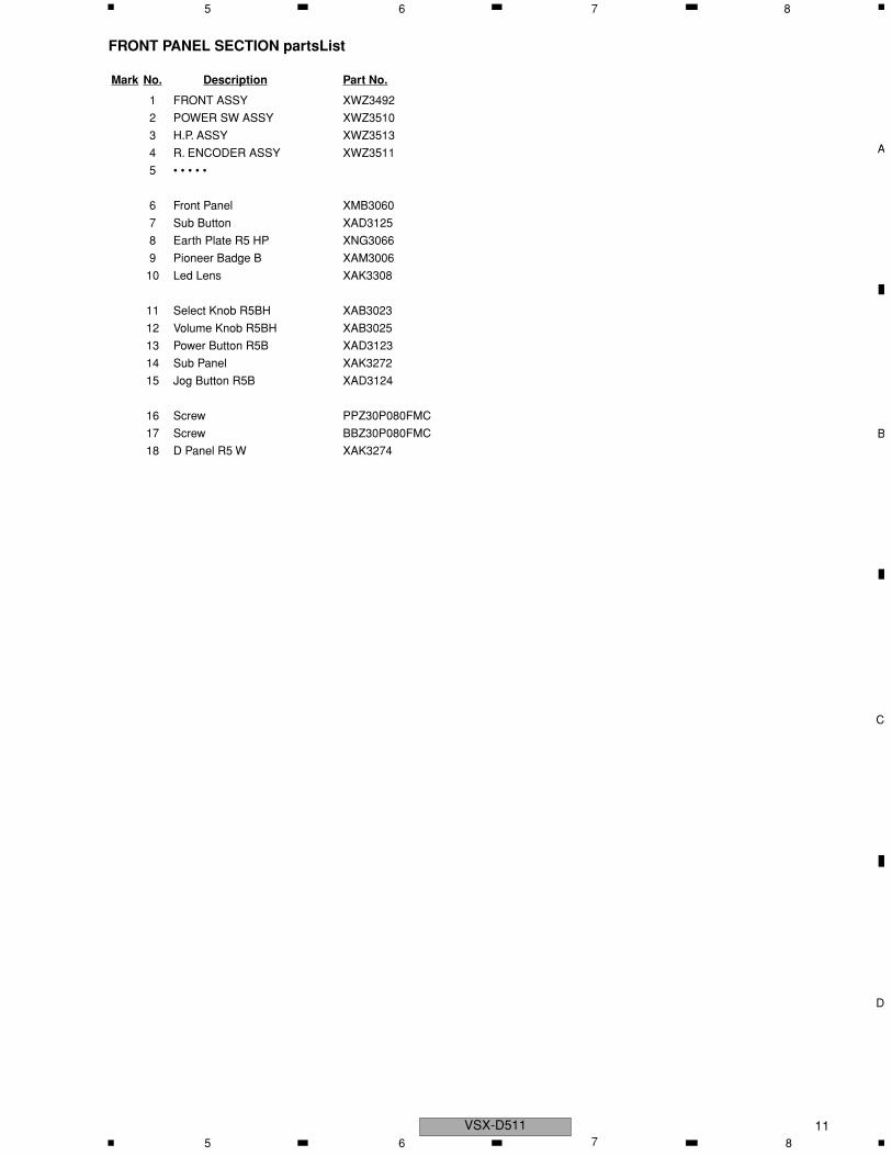
FRONT PANEL SECTION partsList
Mark No. Description Part No.
1 FRONT ASSY XWZ3492
2 POWER SW ASSY XWZ3510
3 H.P. ASSY XWZ3513
4 R. ENCODER ASSY XWZ3511
5 • • • • •
6 Front Panel XMB3060
7 Sub Button XAD3125
8 Earth Plate R5 HP XNG3066
9 Pioneer Badge B XAM3006
10 Led Lens XAK3308
11 Select Knob R5BH XAB3023
12 Volume Knob R5BH XAB3025
13 Power Button R5B XAD3123
14 Sub Panel XAK3272
15 Jog Button R5B XAD3124
16 Screw PPZ30P080FMC
17 Screw BBZ30P080FMC
18 D Panel R5 W XAK3274
5 6 7 811

A
B
C
D
1 2 3 4
VSX-D51112
3. BLOCK DIAGRAM AND SCHEMATIC DIAGRAM3.1 BLOCK DIAGRAM
1
1
3
1
AXQ7231
CN101
10
CN201
7
CN307
IC101
TC9273F-007(FUNCTION SEL)
IC303
IC1901
IC302
IC302
IC104
IC102NJU7312AM
IC9701
IC9101
IC9508
IC9504
IC9503
IC9502
(ADC)
(DIR)
(DAC) (FL/FR)
(EXP/DSP)
(SL/SR)
(C)
(SW)
(CODEC)
(for DECODE)
(SP config)
IC9501
BS62LV 1024TC-70(RAM for AAC)
PDN030A(ROM for DECODE)
TC74VHC574F
TC74VHC574F
CRYSTAL DSP
A
M
J
31
7
1 5
9
CN1047
5
1
CN1901
6
CN9101
2
3
5
3
2
5
15
4
3
2
123
32
43
39-40
11-13
1022
30
27
2826
2 1
IC97022 1
IC97033 1
IC97035 7
IC97042 1
IC92013 1
IC97052 1
AK4586 NJM4558MD (LPF)
NJM4558MD (6dB AMP)
NJM2100M
TC9601NJU7313AM
4
6
3
8
7
20
2119
1211
10
9
5
1
7
5
9
10 11
N
9
5
7
3
9
5
7
311
11IC351
IC352 (Y SEL)
(C SEL)
8
X
CN107
1
K
(8 16bit)
S. VIDEO ASSY
6CH IN ASSY
DIGITAL IN ASSY
D.D & INPUT ASSY
1 2 3 4
A
B
C
D
5 6 7 8
VSX-D511
14.1/24.1 14.7/27.3 13.8
IC103
IC105
IC106
IC107
IC107
Q112Q303
Q603
Q601
Q1552
Q653
Q651
Q632
Q631
uPC2570(PRE AMP)
LECN101
14
CN302
1
11
15
17
31
34
33
36
6
9
5 7
5 7
3 1
5 7
IC601
2426
IC60224 26
IC601 RY751
RY753
RY752
22 15
U
BH
CN702 6
CN15516
CN106
4CN6019
8 5
1 11
+12V
-12V
T1POWERTRANSFORMER
T51
AC IN
D801–D804
U+5V
D51-D54RY51
IC51
IC801
T+12VIC805
CN101IC802
NECK+B
POWER AMPIC601, IC602
NECK-B
D702
D701
+BVL
+BVH
-BVH
-BVL
FL AC
FL AC
Q701
Q702
B
BA
D+5VD721–D724
IC803
A+5VIC804
CN101
EA
CN101A
CN402O
IC301
(CONPONENT SEL)
L9
5
7
1
11
36
VIDEO ASSY
AM
P IN
PU
T A
SS
Y
AMP & PRIMARY ASSY
5 6 7 813
A
B
C
D
1 2 3 4
VSX-D51114
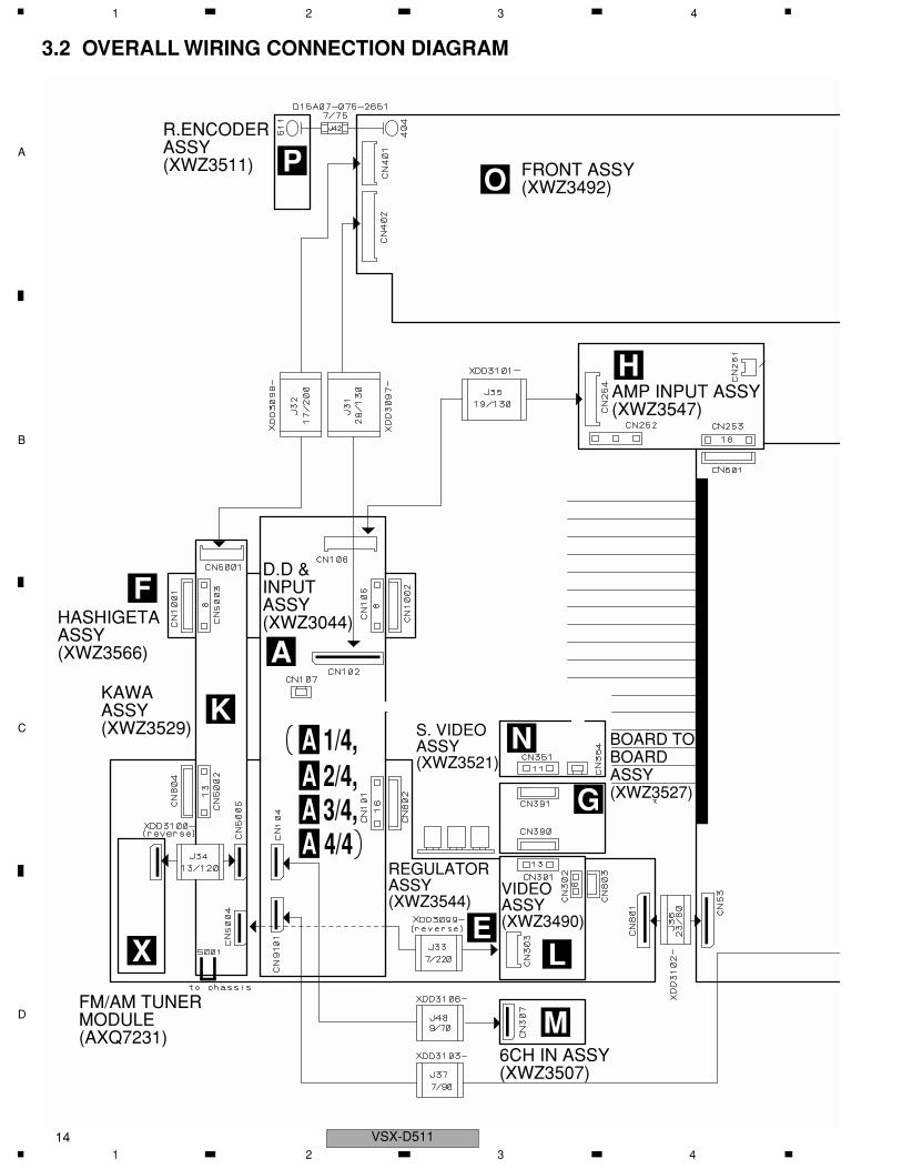
3.2 OVERALL WIRING CONNECTION DIAGRAM
FRONT ASSY(XWZ3492)O
BOARD TOBOARD ASSY(XWZ3527)
S. VIDEOASSY(XWZ3521)
N
G
R.ENCODER ASSY(XWZ3511) P
D.D & INPUT ASSY(XWZ3044)
A
REGULATOR ASSY(XWZ3544)
E
6CH IN ASSY(XWZ3507)
M
VIDEO ASSY(XWZ3490)
FM/AM TUNER MODULE(AXQ7231)
LX
HASHIGETA ASSY(XWZ3566)
F
AMP INPUT ASSY(XWZ3547)
H
KAWA ASSY(XWZ3529)
KA 1/4,A 2/4,A 3/4,A 4/4
1 2 3 4
A
B
C
D
5 6 7 8
VSX-D511
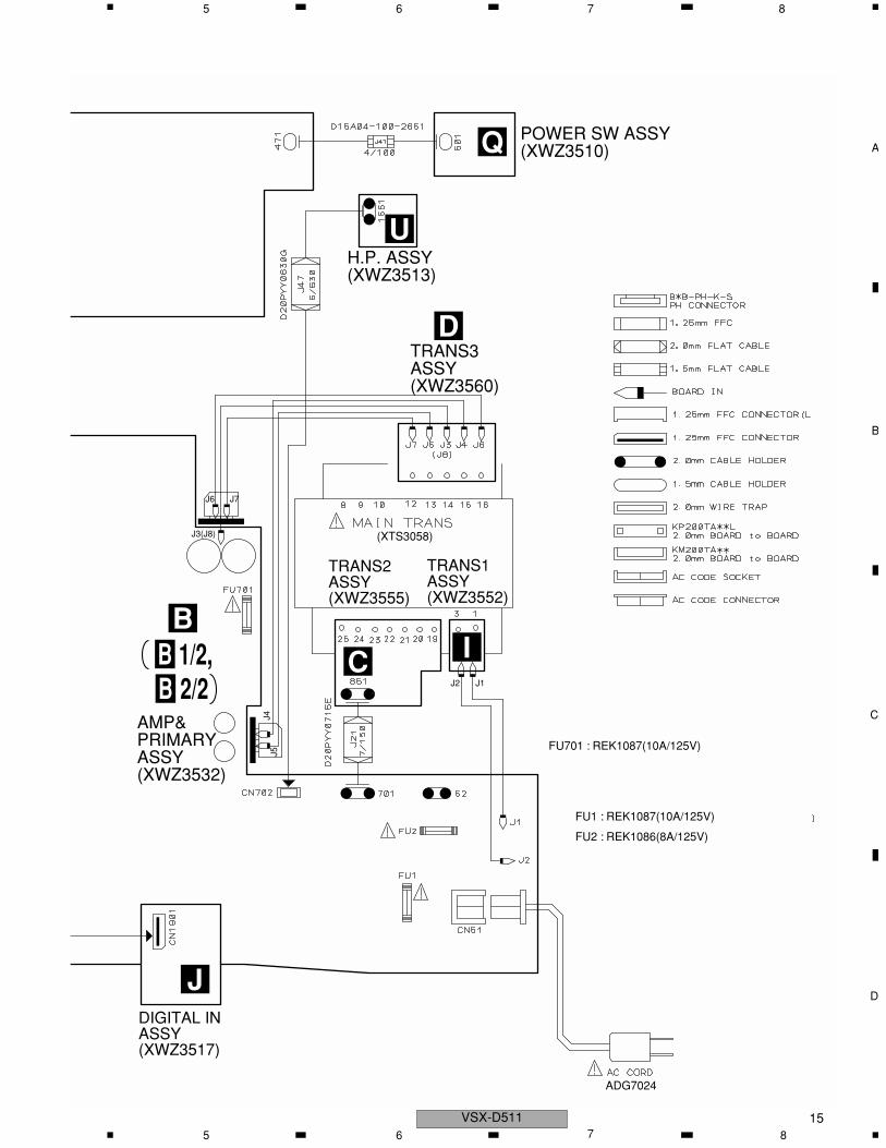
FU1 : REK1087(10A/125V)
FU2 : REK1086(8A/125V)
FU701 : REK1087(10A/125V)
(XTS3058)
ADG7024
DIGITAL IN ASSY(XWZ3517)
J
POWER SW ASSY(XWZ3510)Q
UH.P. ASSY(XWZ3513)
TRANS3 ASSY(XWZ3560)
D
TRANS2 ASSY(XWZ3555)
TRANS1 ASSY(XWZ3552)
C I
AMP&PRIMARY ASSY(XWZ3532)
B
J3(J8)
J7J6
J1J2
J4J5
B 1/2,B 2/2
5 6 7 815

A
B
C
D
1 2 3 4
VSX-D51116
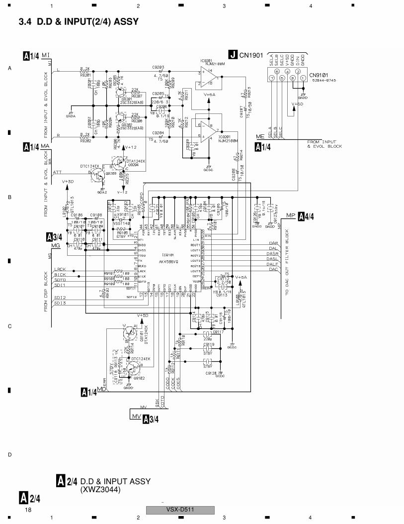
3.3 D.D & INPUT(1/4) ASSY
A
D.D & INPUT ASSY(XWZ3044)
A 1/4
A 1/4A 2/4
CN802E
1 2 3 4

A
B
C
D
5 6 7 8
VSX-D511
A 1/4
CN
402
O
A 2/4
A 4/4
A 4/4
A 2/4A 4/4 A 3/4,4/4
A 2/4 A 2/4 A 3/4CN1002F
CN307M: The power supply is shown with the marked box.
,
5 6 7 817
A
B
C
D
1 2 3 4
VSX-D51118
3.4 D.D & INPUT(2/4) ASSY
AD.D & INPUT ASSY(XWZ3044)
A 2/4
A 2/4
A 1/4
A 4/4
A 1/4
A 1/4
A 3/4
CN1901J
A 3/4
A 1/4
1 2 3 4

A
B
C
D
5 6 7 8
VSX-D511
A 2/4
CN
254
H
A 1/4
A 1/4
A 1/4A 1/4
A 1/4
5 6 7 819

A
B
C
D
1 2 3 4
VSX-D51120
3.5 D.D & INPUT(3/4) ASSY
AA 3/4
A 1/4
1 2 3 4

A
B
C
D
5 6 7 8
VSX-D511
D.D & INPUT ASSY(XWZ3044)
A 3/4
A 3/4
A 2/4A 1/4
A 2/4
5 6 7 821

A
B
C
D
1 2 3 4
VSX-D51122
3.6 D.D & INPUT(4/4) ASSY
A
D.D & INPUT ASSY(XWZ3044)
A 4/4
A 4/4
A 1/4
A 1/4
A 1/4
A 2/4 A 1/4
1 2 3 4

A
B
C
D
5 6 7 8
VSX-D511
A 4/4
A 1/4
5 6 7 823

A
B
C
D
1 2 3 4
VSX-D51124
3.7 AMP & PRIMARY(1/2), TRANS2 and TRANS3 ASSYS
AMP&PRIMARY ASSY (XWZ3532)B 1/2
B 2/2
CN
253
H
B 1/2
1 2 3 4

A
B
C
D
5 6 7 8
VSX-D511
REK1087(10A)
C D
TRANS3 ASSY
D
TRANS2 ASSY
(XWZ3555)
C
(XWZ3560)
POWER TRANSFORMER
1551U
CAUTION : FOR CONTINUED PROTECTION AGAINST RISK OF FIRE.REPLACE ONLY WITH SAME TYPE NO. 49101.6 FOR IC853 MFD, BY LITTELFUSE INC.
CAUTION : FOR CONTINUED PROTECTION AGAINST RISK OF FIRE.REPLACE ONLY WITH SAME TYPE NO. 491010 FOR IC604, IC605, IC606, AND IC607 MFD, BY LITTELFUSE INC.
CAUTION : FOR CONTINUED PROTECTION AGAINST RISK OF FIRE.REPLACE ONLY WITH SAME TYPE NO. 491001 FOR IC603 MFD, BY LITTELFUSE INC.
CAUTION : FOR CONTINUED PROTECTION AGAINST RISK OF FIRE.REPLACE ONLY WITH SAME TYPE NO. 49101.6 FOR IC851 AND IC852 MFD, BY LITTELFUSE INC.
CAUTION : FOR CONTINUED PROTECTION AGAINST RISK OF FIRE.REPLACE ONLY WITH SAME TYPE NO. 491.125 FOR IC701 AND IC702 MFD, BY LITTELFUSE INC.
B 2/2
• NOTE FOR FUSE REPLACEMENTFOR CONTINUED PROTECTION AGAINST RISK OF FIRE.REPLACE WITH SAME TYPE AND RATINGS ONLY.
CAUTION - B 1/2
5 6 7 825
A
B
C
D
1 2 3 4
VSX-D51126
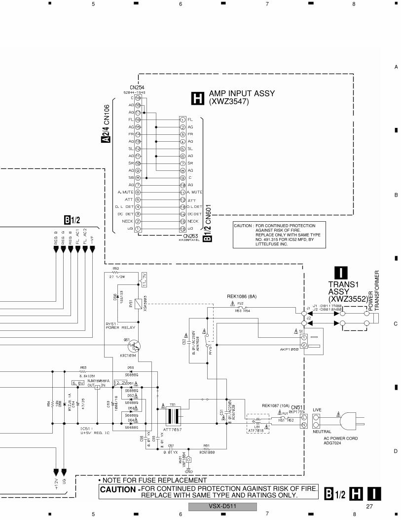
3.8 AMP & PRIMARY(2/2), REGULATOR, AMP INPUT and TRANS1 ASSYS
E F G
CN
101
B 1/2
A1/4
A1/4
CN
5002
CN302L
BOARD TOBOARD ASSY(XWZ3527)
G
REGULATOR ASSY(XWZ3544)
E
HASHIGETA ASSY(XWZ3566)
F
AMP&PRIMARY ASSY(XWZ3532)
B 2/2
B 1/2
KC
N50
03K
CN351N
CN301L
CN
105
1 2 3 4
A
B
C
D
5 6 7 8
VSX-D511
REK1086 (8A)
H I
CN
106
A2/4
CN
601
B1/2
B 1/2
PO
WE
R
TR
AN
SF
OR
ME
R
LIVE
NEUTRAL
REK1087 (10A)
AC POWER CORDADG7024
• NOTE FOR FUSE REPLACEMENTFOR CONTINUED PROTECTION AGAINST RISK OF FIRE.REPLACE WITH SAME TYPE AND RATINGS ONLY.
CAUTION -
CAUTION : FOR CONTINUED PROTECTION AGAINST RISK OF FIRE.REPLACE ONLY WITH SAME TYPE NO. 491.315 FOR IC52 MFD, BY LITTELFUSE INC.
AMP INPUT ASSY(XWZ3547)H
TRANS1 ASSY(XWZ3552)
I
B 1/2
5 6 7 827

A
B
C
D
1 2 3 4
VSX-D51128
3.9 VIDEO, 6CH IN and S.VIDEO ASSYS
L M
6CH IN ASSY(XWZ3507) M
VIDEO ASSY(XWZ3490) L
CN
803
EC
N39
0G
CN5004KCN104A 1/4
1 2 3 4

A
B
C
D
5 6 7 8
VSX-D511
N
S. VIDEO ASSY(XWZ3521)N
CN
391
G
5 6 7 829
A
B
C
D
1 2 3 4
VSX-D51130
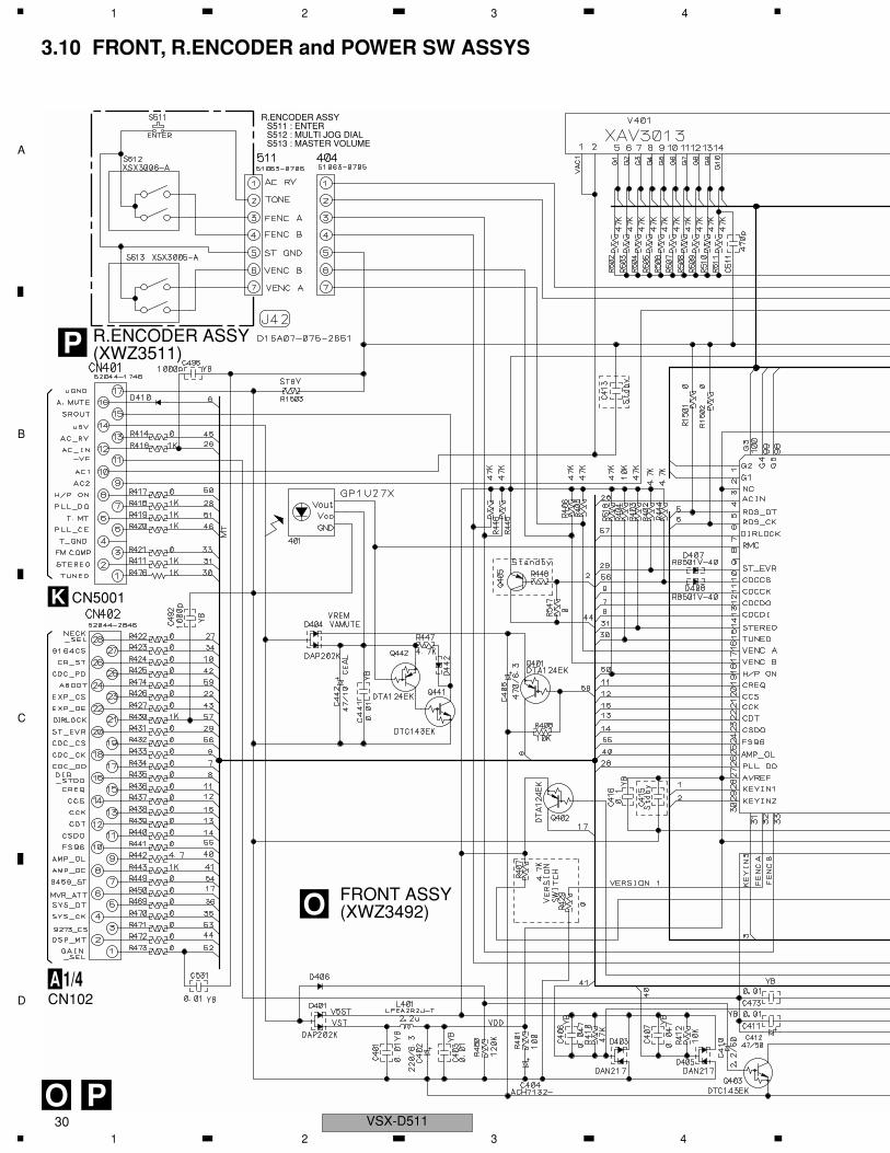
3.10 FRONT, R.ENCODER and POWER SW ASSYS
O P
FRONT ASSY(XWZ3492)O
R.ENCODER ASSY(XWZ3511)P
CN102A 1/4
CN5001
R.ENCODER ASSYS511 : ENTERS512 : MULTI JOG DIALS513 : MASTER VOLUME
K
1 2 3 4

A
B
C
D
5 6 7 8
VSX-D511
MONITOR
FL DIMER
IMPUT ATT
MIDNIGHT
LOUDNESS
PDG268B
O Q
POWER SW ASSY(XWZ3510)
Q
FRONT ASSYS451 : SIGNAL SELECTS452 : MONITORS453 : MIDNIGHTS454 : LOUDNESSS455 : TONES456 : SETUPS457 : ADVANCED SURRS458 : DIRECTS459 : FL DIMERS460 : IMPUT ATTS461 : MPXS462 : BANDS463 : STANDARDS464 : TUNING(+)S465 : TUNING(–)S466 : STATION(+)S467 : STATION(–)S468 : MULTI JOGS476 : CLASS
POWER SW ASSYS501 : POWER STANDBY/ON
5 6 7 831

A
B
C
D
1 2 3 4
VSX-D51132
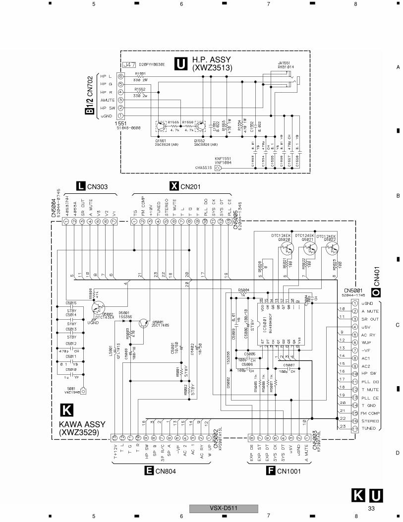
3.11 DIGITAL IN, H.P. and KAWA ASSYS
J
DIGITAL IN ASSY(XWZ3517)J
CN
9101
A2/4
1 2 3 4
A
B
C
D
5 6 7 8
VSX-D511
U
KAWA ASSY(XWZ3529)
K
CN
401
O
CN804E CN1001F
CN303L CN201X
K
U H.P. ASSY(XWZ3513)
CN
702
B1/2
5 6 7 833

A
B
C
D
1 2 3 4
VSX-D51134
3.12 FM/AM TUNER MODULE
FM FRONT END
MW RF TUNING BLOCK
FM/AM TUNER MODULE (AXQ7231)X
OSC : 981 - 2052kHz 9k step
(AM)
(AM
)
(AM
)
(AM) (AM)
(AM)
(FM)
(FM
)(F
M)
(FM)
(FM)
(FM)
(FM) (FM)
(FM
)
(FM
)
X
1 2 3 4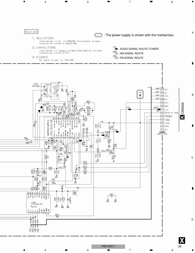
A
B
C
D
5 6 7 8
VSX-D511
L201
ATE7003
PLL IC
AM
/FM
IF+
MP
X IC
ATF7026
: AUDIO SIGNAL ROUTE (TUNER)(TX)
: AM SIGNAL ROUTE(AM)
: FM SIGNAL ROUTE(FM)
(AM)
(AM)
(FM)
(AM
)(A
M)
(AM
)
(AM
)
(AM
)
(AM
)
(FM
)
(AM
)
(FM)
(TX)
(TX)
(TX)
(TX)
(TX)
(FM)
: The power supply is shown with the marked box.
X
CN
5005
K
5 6 7 835

A
B
C
D
1 2 3 4
VSX-D51136
4. PCB CONNECTION DIAGRAM
NOTE FOR PCB DIAGRAMS :1. Part numbers in PCB diagrams match those in the schematic diagrams.2. A comparison between the main parts of PCB and schematic diagrams is shown below.
3. The parts mounted on this PCB include all necessary parts for several destinations. For further information for respective destinations, be sure to check with the schematic diagram.4. View point of PCB diagrams.Symbol In PCB
DiagramsSymbol In SchematicDiagrams
Part Name
B C E
D
D
G
G
S
S
B C E
B C E
D G S
B C E B C E
B C E
Transistor
Transistorwith resistor
Field effecttransistor
Resistor array
3-terminalregulator
CapacitorConnector
P.C.Board Chip Part
SIDE A
SIDE B
1 2 3 4
A
B
C
D
5 6 7 8
VSX-D511
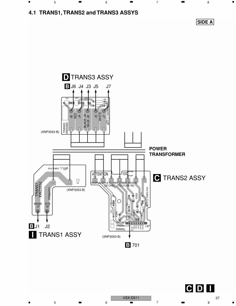
4.1 TRANS1, TRANS2 and TRANS3 ASSYS
NP
DE CHEZ LITTELFUSE INC.REMPLACER LE IC LINKS COMME INDIQUE.
XWZ3555 J21
FL
AC
FL
AC
RE
G
RE
GR
EG
DR
EG
DR
EG
TRANS2
NP
NP
XWZ3556
CM
KS
-P3X
ATTENTION
1
C85
3
IC85
3IC
852
IC85
1
851
R85
1
C85
2
C85
1
R85
2
R85
3
CMKS-P3X
BROWN BLUE
XW
Z35
52
PR
IMA
RY
TR
AN
S1
J2J1
NP
J7
BLA
CK
BLU
EJ8
XW
Z35
60T
RA
NS
3
NP
NP
RE
DJ6 J5J4 J3
WH
ITE
CM
KS
-P3X
C881R881
R882
C883C882
(XNP3053-B)
(XNP3053-B)
(XNP3053-B)
TRANS3 ASSYD
TRANS2 ASSYC
I701B
J1 J2B
J6 J4 J3 J5 J7B
POWER TRANSFORMER
TRANS1 ASSY
C D I
SIDE A
5 6 7 837

A
B
C
D
1 2 3 4
Q9601 Q9602
Q9203
IC9506
VSX-D51138
4.2 D.D & INPUT ASSY
D.D & INPUT ASSYA
CN1002F
CN402O
CN254H
Q9603 Q9604 Q9605 Q9606IC102IC103 Q9611
Q9609 Q0608 Q9607Q9610 Q9601 Q9602 IC9601
Q111
IC301Q107 Q108Q109 Q110
IC110IC105IC106IC107 Q112
A
SIDE AC
N10
2
CN106 CN105
1 2 3 4

A
B
C
D
5 6 7 8
CN1002F
04 Q9605 Q9606 QIC9601
CN105
VSX-D511
CN802E
CN1901JCN307M
Note : The pin of function IC(IC101 TC9273F-007)can be checked from side-A by the through-hole round. The pin No. is printed on the side-A.
9611 Q9601 Q9602 IC9101 IC9504IC9507 IC9501
Q9203 Q9204
IC9506 IC9102 IC9505 IC9508
IC9201IC104
IC9812Q9201 Q9202
(XNP3056-C)
A
SIDE A
CN101
CN9101CN104
5 6 7 839

A
B
C
D
1 2 3 4
9705IC9707
IC9704IC9705
VSX-D51140
D.D & INPUT ASSYA
IC9502IC9503 Q9552Q9551
IC101IC9811
ICIC9703
IC9701IC9702
A
SIDE B
1 2 3 4

A
B
C
D
5 6 7 8
IC9703
IC9701IC9702
VSX-D511
IC9705 IC112IC9707
IC9704IC9705
(XNP3056-C)
A
SIDE B
5 6 7 841

A
B
C
D
1 2 3 4
NP
PRODUCTION C
WHITERED
SD.
E
J4J5
AN
P G
D5SBA20
CM
KS
-P3X
rd surface
C60
6
C60
7
C609
C61
2
C614
C615
3 C704
D60
1
D6
D702
IC601 R61
5
Q604
Q6
Q602
R61
0
R61
1
R61
7
R61
9
R62
1
R6
W508
W561
W57
9
W58
0W
516
W51
7
W56
4
W56
3
W54
1
W542
W565
W562
C
C60
4
DJ5D
85C
155U
Q
IC
IC
VSX-D51142
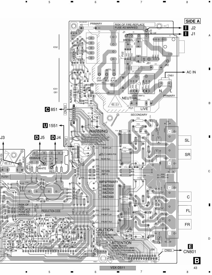
4.3 AMP INPUT and AMP ASSYS
31
31
31
STOP
-12VGND
AGFL
UG
SL
AG
FR
AG
SL
AG
SR
AG
FL
C
ATT
DC
AG
AG
AG
AT
T
DC
UG
FR
A.MUTE
OL
NECK
SR
SB
AG
AGA
G
A.M
UT
E
OL
NE
CK
AG
UG
AG
J35
CMKS-P3X
XWZ3548XWZ3547
AMP INPUT
+12V
FAN+FAN-
J22
NP
AGC
119
14
8
5
1 16
W60
6
CN253
CN255
R270
R26
8
D25
4
W61
3
W62
9
W60
5
W62
8
R25
1
R25
6
R25
2
R25
5D
253
W60
7
CN
251
R264W626
IC251
Q25
4
C25
3
CN252
C252
R26
7
Q253 Q25
1
R26
6
Q25
5
R26
2
C25
4
R26
3
R25
7R
261
W61
0Q
256
W60
9
W68
4
W60
4
Q25
2
D25
2
W627R26
0
R25
9
W61
4
W60
8
R265
R25
8
D25
1R
253
W68
2
Q25
8
W611
W61
2
R269
W73
6
Q25
7
C25
1C
N25
4
NP
NP
NP
CMKS-P3X
J701J701
BOND
BOND
J3
FUSE AMARKE
RISK OFFIRE-REPLAC
AGFL
FR
AG
SL
AG
SR
AG
C
AG
AMUTE
ATT
OL
DCNECK
UG
WHITE
RED
BLUEJ8
J6
J7
4910
10
FU701
VL+
VL-
AN
P G
NE
CK
+VH
+
NE
CK
+
VL+
VH
-
NE
CK
-
VL-
NE
CK
-
1
D5S
BA
20
22
491.
125
GRAY
GRAY
BLA
CK
491.125
E
E
word surface
26
1
116
W683
W578IC701
C601
C602
C60
5 C61
1
C613
C63
1
C63
3
C63
4C
635
C63
6
C637
C638
C65
1
C65
2
C65
5
C65
6
C65
7 C658
C65
9
C66
0C66
1
C66
2
C663 C664
C665
C66
6
C691
C70
1
C70
2
C70
C705
C706
CN
601
D63
1
D632
D633
D634
D651 D65
2
D653
D65
4
D70
1
H701 H702
IC602
IC60
6
IC60
7
R66
5
R66
6
R63
8
Q633
Q65
6
Q603
Q65
2
Q63
1
Q65
5
Q63
2
Q65
4
Q601
Q703
Q65
1
Q701
Q702
Q704
R601
R602
R603
R604R605
R606
R607
R608
R60
9
R613
R61
4
R631
R632R633
R634
R63
5
R63
6R63
7
R63
9
R640
R641
R64
2
R643
R644
R64
5R65
1
R652
R65
3
R65
4
R65
5
R65
6
R65
7
R65
8
R65
9
R66
0
R66
1
R66
2
R66
3
R66
4
R66
7
R66
8
R669 R670
R67
1
R672
R67
3
R674
R691
R701
R702
R703
R704
R705
R706
R707
R708
W505
IC702
C653
W50
3
W501
W502
W575
W576
W507
W554
W553
W550
W55
9
W574
W573
W557
W556
W51
0
W51
1
W51
2
W504
W552
W53
0
W555
W53
1
W53
2
W551
W53
3
W51
5
W53
4
W50
6
W53
5
W53
7
W53
8
W53
6
W529
W558
W53
9
W54
0
W56
0
W51
3
W577
W51
4
W594
W572
W595
Q692
Q65
3
C70
7
Q691
C654
C63
2W
730
C603
C692
B H
SIDE A
AMP INPUT ASSYH
AMP&PRIMARY ASSYBCN106A
Q604Q606Q605
Q602
Q601Q603
IC601
IC605IC604
IC603
Q632
Q704Q702IC702Q703
Q701IC701
Q631
IC606IC607
Q656Q683
IC602
Q633
Q655
Q697Q696Q681Q682
Q652Q654
Q651Q653
J7D
J6D
(XNP3053-B)
(XNP3053-B)
Q255Q254Q252
Q256
Q253
Q251IC251
Q257Q258
J3D
CN254
1 2 3 4
A
B
C
D
5 6 7 8
J701
J3
FUSMAR
RISFIRREP
FU701
VL+
AN
P G
NE
CK
+VH
+
VL+
NE
CK
-
VL-
491.
125
Y
5
W683
W57801
C601
C602
C60
5 C61
1
C613
H701 H
Q603
Q601
703
R601
R603
R604R605
R606
R607
R60
9
R613
R64
2
02
W507
W55
9
W51
5W
506
W53
7
W53
8
W53
6
W558
W53
9
W54
0
7
C603
J3D
VSX-D511
1
XWZ3580
NP
NP
PRODUCTION CODE
UG
RE
G
GN
D
RE
G
DR
EG
DR
EG
LN
TUBE SIDE
BLUE
GRAY
WHITERED
BLACKRED
J44
4910
01
E ASKED.
K OFE-LACE
491.315
J11
LINKS AS MARKED.MED.
DR
EG
DR
EG
RE
G
GN
D
RE
G
-VF
AC
1A
C2
W U
PA
CR
YU
+5V U
G
+12
VA
RY
R/C
RY
491010
231
BROWN
FUSE AS MARKED.
COMME INDIQUE.
FU
2
FU
3
RISK OF FIRE-REPLACE
FU1
XWZ3532XWZ3533
ATTENTIONREMPLACER LE IC LINKS
CAUTIONREPLACE IC
BY LITTELFUSE INC.
PRIMARY
SECONDARY
PRIMARYSECONDARY
J1 J2
J4J5
FLACFLAC
REG
REG
REG
DREG
DREG
DE CHEZ LITTELFUSE INC.
4910
10
2
J12 J13
NJM
78M
56J2
1
VL-
VL-VL+
AN
P G
VH
+
VL+
VH
-
VH-
AMP&PRIMARY
THIS PRODUCT CONTAINS LEAD INSOLDER AND CERTAIN ELECTRICALPARTS CONTAIN CHEMICALS WHICH AREKNOWN TO THE STATE OF CALIFORNIATO CAUSE CANCER, BIRTH DEFECTS OROTHER REPRODUCTIVE HARM.HEALTH & SAFETY CODESECTION 25249.6 - PROPOSITION 65
J36
REAR Lch
REAR Rch
RETURN
AMP G
CENTER
FRONT Lch
WARNING
FRONT Rch
AN
P G
XWZ3534
D5SBA20
22
HP RHP GHP L
U GNDHP SWMUTE
VH+
BLA
CK
C
FR
J47
FL
CMKS-P3X
J52
NC
SR
SL1
1
J51
CM
KS
-P3X
NP
NP
HP
SW
word surface
61
51
52
53
CN51
C53
C54
C55
C56
C57
C60
6
C60
7
C60
8
C609
C61
0
C61
2
C614
C615
C61
6
C703 C704
C711
C712
D724
D722
D721
D723
CN
752
D55
D56
D57
D58
D60
1
D60
2
D603
D60
4
D605D606
D702
D712
D751
D752
D755D756
H51 H52
H53
H54
H55
H56
702
IC52
IC601
IC60
3
IC60
4
IC605
KN51
KN601
R61
5
R61
6
L51
L751
L752
L753
L761
L762
Q51
Q604
Q605
Q602
Q60
6
RY51
R51
R52
R53
R54
R602
R608
R61
0
R61
1
R61
2
R61
4
R61
7
R61
8
R61
9
R62
0
R62
1
R62
2
R623
R62
4
R62
5
R62
6
R62
7
R711
R751
R752
R755
R761
R762
RY753
T51
W52
8
CN53
W584
W571
W73
4
W526
W598
IC51
C52
C51
W508
W561
W589
W590
W591
W636
W58
2
W58
1
W57
9
W58
0
W525
W661
W66
2
W509
W51
6
W51
7
W56
4
W56
3
W56
0
W54
1
W585
W569
W568
W566
W52
4
W545
W596
W587
W544
W586
W542
W543
W565
W51
9W
520
W52
1
W52
3
W597
W588
W634
W635
W63
9
W562
W567
W649
W66
6
W66
8
W66
7
W63
8
W63
7
W64
2
W64
0
W64
1
W52
2
W518
W615W
665
W66
3
W66
4
D51
D52
D53
D54
D711
701
C771
W54
7
W592
C75
4
W549
C75
8C
759
C770
C708
W61
9
W61
8
W617
C769
R763
R764
W59
3
C76
4
C76
3
C762
C76
1
C75
2
C755
RY751
RY752
R753
W546
R756
R75
4
C751
C75
7
C756
W73
7C
753
C76
5C
766
W59
9
W732
C77
6
W731
C77
5
C60
4
W583
CN
751
W75
8
W735
W733
W57
0
W54
8
CN
702
B
SIDE A
II
J4DJ5D
851C
1551U
Q51
IC52
IC51
AC IN
NEUTRAL
LIVE
J2J1
CN801E
CN53
CN
701
CN
702
5 6 7 843
A
B
C
D
1 2 3 4
(XNP3052-B)
VSX-D51144
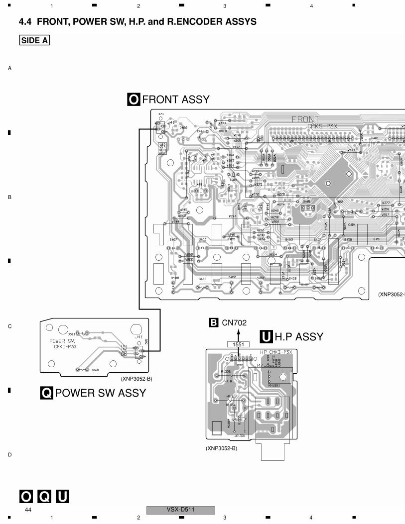
4.4 FRONT, POWER SW, H.P. and R.ENCODER ASSYS
FRONT ASSYO
CN702B
POWER SW ASSYQ
O Q U
SIDE A
H.P ASSYU
(XNP3052-B)
(XNP3052-B)
1551
1 2 3 4

A
B
C
D
5 6 7 8
ASSY
VSX-D511
CN5001K
CN102A
R.ENCODER ASSYP
O P
SIDE A
(XNP3052-B)
(XNP3052-B)
CN
402
CN
401
5 6 7 845

A
B
C
D
1 2 3 4
U
IC401 Q40
VSX-D51146
FRONT ASSYO
R.ENCODER ASSYP
(XNP3052-B)
O P
SIDE B
Q401 Q441 Q442
1 2 3 4

A
B
C
D
5 6 7 8
VSX-D511
POWER SW ASSYQ
H.P ASSYU
(XNP3052-B)
(XNP3052-B)
(XNP3052-B)
O Q U
SIDE B
IC481IC401 Q402 Q405 Q403 Q481 Q482 Q483 Q471
5 6 7 847

A
B
C
D
1 2 3 4
IDE A
(XN
KK
Q5001
VSX-D51148
4.5 REGULATOR, HASHIGETA and KAWA ASSYS
CM
KI-
P3X
81
81
HA
SH
IGE
TA
XW
Z3566
UG
A M
UT
E
U+
5V
SY
S.D
T
A M
UT
E
U+
5V
UG
SY
S.D
TS
YS
.CK
SY
S.C
KE
XP
.DT
EX
P.S
TE
XP
.CE
EX
P.D
TE
XP
.ST
EX
P.C
E
CN1001
CN1002
DG
T.L
-12V
D+
5V
AG
RE
TU
RN
DR
EG
RE
G G
RE
G B
-12V
RE
G G
KNIFE SPACE
+12
V
+12
V
-VF
AC
2A
C1
STBY
XNP3053-B
U+
5V
6 1
W U
P
AC
2
-VF
NJM
78M
12
SP-R
/C
NJM
78M
05
NJM78M05
T+
12V
AD
G
REG -B
UG
SW
OU
T
NC
16 1
RE
G B
AC
RY
NJM
79M
12
AC
RY
AG
RE
G B
DR
EG
DR
EG
NJM78M12
AD
+5V
UG
U+
5VDA
G
T.G
T.R
UG
H.P
SW
+12
V
SW
OU
T
RE
GU
LAT
OR
CMKS-P3X
AD
G
REG +B
-12V
W.U
P
SP
-A
A R
Y
R/C
RY
CM
KS
-P3X
P I D
REG +B
AC
1
T.L
T.G
T.R
HP
SW
NC
XW
Z35
44
+12V
AG
UG
ADG
DG
13 1
D +5V
J36
RE
G B
DR
EG
ATTENTION
1 23
C81
2
W632
R801
W603
W631
W747
W655
W743
W75
1
W75
0
W672
C803
W660
W625
W621
IC805
W657
C814
CN803
W60
1
IC804
C801
C807
W62
0
W648
D81
0
C81
1
W658
W643
W746
CN802
Q803
D80
1
D80
2
D80
3
W674
W644
D80
4
W633
W645
W675
W673
W647
W60
0
W630
Q804 W75
2
CN801
IC80
3IC
802
IC80
1
D80
9Q801
C809
W754
W67
1
W622
C808
W748801
C804
C813
C806
W753
C805
CN804
W697
C802
W602
C81
0
Q802
W74
5
E F
SIDE A S
(XNP3053-B)
(XNP3053-B)
Q805
Q803Q806Q801
Q804
Q802
IC804
IC805
REGULATOR ASSYE
HASHIGETA ASSYF
CN53BCN302L
CN101A
CN105A
IC802
IC803
IC801
CN1002
CN802
CN801CN803
1 2 3 4

A
B
C
D
5 6 7 8
CN101
VSX-D511
K
SIDE BSIDE A
(XNP3052-B) (XNP3052-B)
KAWA ASSYK KAWA ASSYK
CN303L
CN201X
CN401O
Q5001
Q5002
Q5020
Q5021
Q5022
IC5001
CN
5001
CN
5005
CN
5004
5 6 7 849

A
B
C
D
1 2 3 4
6CH INM
(XNP3052-B)
BOAG
VSX-D51150
4.6 DIGITAL IN, 6CH IN, VIDEO and BOARD TO BOARD ASSYS
AD
G
VID
EO
1
+5V
AD
G
SR
5 1
13 1
CM
KI-P
3X
+5V
AD
G
4053INH-5V
-5V
VID
EO
3
AD
G
4053A
VID
EO
2
UG
FR
ON
TV
J38
4053
INH
UG
VID
EO
1 SR
AD
G
4053
A
VID
EO
3
-5V
VID
EO
2
AD
G
FR
ON
TVB
OA
RD
TO
BO
AR
D
+5V
AD
G
111
XW
Z3527
CN392
W749
CN390391
CN391W756
W757
G J L M
SIDE A
DIGITAL IN ASSYJ6CH IN ASSYM
CN9101A
CN104A
CN351N
CN803E
CN5004K
(XNP3052-B)
(XNP3052-B)
(XNP3052-B)
(XNP3053-B)
BOARD TO BOARD ASSYG
VIDEO ASSYL
Q302
Q301
CN1901
CN307
CN
302
CN
391
CN
303
1 2 3 4

A
B
C
D
5 6 7 8
IN ASSY
CN104A
CN307
VSX-D511
G J L M
SIDE B
DIGITAL IN ASSYJ6CH IN ASSYM
(XNP3052-B)
(XNP3052-B)
(XNP3053-B)
(XNP3052-B)BOARD TO BOARD ASSYG
VIDEO ASSYL
IC1902IC1903
IC304
IC303
IC302
IC305
IC1901
IC301
Q303
51
131
1
CM
KI-
P3X S
R
UG
AD
G
AD
G
AD
G
-5V
V3
V2
V1
J38
F V
-5V
+5V
AD
G
4053INH
4053
INH
4053
A
AD
G
V1
V3
F V
UG
SR
V2
AD
G
-5V
4053A
AD
G
+5V
BO
AR
D T
O B
OA
RD
+5V
XWZ3527
5 6 7 851

A
B
C
D
1 2 3 4
VSX-D51152
4.7 FM/AM TUNER MODULE
(ANP7338-B)
(ANP7338-B)
CN5005K
FM/AM TUNER MODULEX
FM/AM TUNER MODULEX
IC201 Q205Q204
Q203IC202
Q201
Q202
X X
SIDE A
SIDE A
SIDE B
SIDE B
CN201
1 2 3 4

A
B
C
D
5 6 7 8
VSX-D511
5. PCB PARTS LIST Parts marked by "NSP" are generally unavailable because they are not in our Master Spare Parts List.The mark found on some component parts indicates the importance of the safety factor of the part.Therefore, when replacing, be sure to use parts of identical designation.When ordering resistors, first convert resistance values into code form as shown in the following examples.Ex.1 When there are 2 effective digits (any digit apart from 0), such as 560 ohm and 47k ohm (tolerance is shown by J=5%, and K=10%).
Ex.2 When there are 3 effective digits (such as in high precision metal film resistors).
5 6 14 7 3
R 5 01 R 0
5 6 2 1
NOTES:
560 Ω47k Ω0.5 Ω1 Ω
RD1/4PU JRD1/4PU JRN2H KRS1P K
56 x 10 1
47 x 10 3
R501R0
561473
5.62k Ω RN1/4PC F562 x 10 1 5621
Mark No. Description Part No.
LIST OF ASSEMBLIES 1..D.D & INPUT ASSY XWX3044 NSP 1..AMP & PS ASSY XWK3052 2..AMP & PRIMARY ASSY XWZ3532 2..REGULATOR ASSY XWZ3544 2..AMP INPUT ASSY XWZ3547 NSP 2..TRANS1 ASSY XWZ3552 2..TRANS2 ASSY XWZ3555 NSP 2..TRANS3 ASSY XWZ3560 2..HASHIGETA ASSY XWZ3566 2..BOARD TO BOARD ASSY XWZ3527 NSP 1..COMPLEX ASSY XWK3037 2..FRONT ASSY XWZ3492 2..6CH IN ASSY XWZ3507 2..POWER SW ASSY XWZ3510 2..H.P. ASSY XWZ3513 2..DIGITAL IN ASSY XWZ3517 2..S. VIDEO ASSY XWZ3521 2..KAWA ASSY XWZ3529 2..R. ENCODER ASSY XWZ3511 2..VIDEO ASSY XWZ3490 1..FM/AM TUNER MODULE AXQ7231
Mark No. Description Part No.
COMPLEX ASSYOTHERS
J 41 (JUMPER WIRED) D15A04-100-2651J 42 (JUMPER WIRED) D15A07-075-2651J 47 (JUMPER WIRED) D20PYY0630E
AMP & PS ASSYOTHERS
J 701 (AWG14 BOARD IN) DB812NBOJ 21 (JUMPER WIRED) D20PYY0715E
A D.D & INPUT ASSY
SEMICONDUCTORSIC9101 AK4586VQIC301 BU4094BCFIC9501 CS493292IC103 M62446FPIC9201 NJM2100M
IC9812 NJM2391DL1-25IC9811 NJM2391DL1-33IC102 NJU7312AM
IC9601 NJU7313AMIC9504 PD8097A
IC9505 TC74LVX244FTIC9502, IC9503 TC74VHC574FIC9506 TC74VHCT244AFTIC9507 TC7WU04FUIC101 TC9273F-007
IC104-IC107, IC9701-IC9705, IC9707 UPC4570G2Q107-Q112, Q9201, Q9202 2SC3326Q9101, Q9204, Q9607, Q9609, Q9610 DTA124EKQ9102, Q9203, Q9608 DTC124EKD9601, D9602 1SS181
D105, D106, D301, D9921 1SS355D107, D108 DAN217D201, D202 RB501V-40D104 UDZS5.1BD101, D102 UDZS6.8B
COILS AND FILTERSL9101, L9501, L9504, L9811, L9812 ATL7002L111-L114, L1601, L1602 QTL1013L9102, L9103, L9502, L9503 QTL1013L9506, L9507 QTL1013
CAPACITORSC9510, C9511 CCSRCH100D50C101-C114, C121-C123 CCSRCH101J50C126-C128, C152-C154 CCSRCH101J50C207, C208, C221, C222 CCSRCH101J50C228, C229, C9160, C9201, C9202 CCSRCH101J50
C9101, C9102 CCSRCH220J50C235, C9117 CCSRCH221J50C9509 CCSRCH271J50C9530, C9731, C9735 CCSRCH331J50C9103, C9110, C9111, C9114, C9503 CCSRCH471J50
C9505, C9507, C9513, C9515, C9518 CCSRCH471J50C9520, C9522, C9525, C9528, C9571 CCSRCH471J50C9611-C9614, C9625, C9639, C9729 CCSRCH471J50C9815, C9816 CCSRCH471J50C9707, C9708, C9721, C9722 CCSRCH820J50
C130-C137, C146-C151, C305 CEAT100M50C9207, C9208, C9523, C9526 CEAT100M50C9105, C9106, C9108, C9116, C9516 CEAT101M10C9551, C9792, C9812, C9814 CEAT101M10C9740 CEAT220M25
C9205 CEAT221M6R3C9112, C9529, C9769, C9770 CEAT2R2M50C9713, C9714, C9727, C9728, C9739 CEAT330M25
Mark No. Description Part No.
5 6 7 853

A
B
C
D
1 2 3 4
VSX-D51154
C9765-C9768 CEAT330M25C144, C145 CEAT3R3M50
C117, C118, C225, C226 CEAT470M50C232, C233, C239 CEAT470M50C155, C156 CEAT471M10C115, C116, C234, C240 CEAT4R7M50C9203, C9204, C9615-C9618, C9811 CEAT4R7M50
C9813 CEAT4R7M50C271, C9703, C9704, C9717, C9718 CKSRYB102K50C119, C120, C124, C125, C138 CKSRYB103K50C141, C171, C172, C179, C180 CKSRYB103K50C183, C199, C223, C224 CKSRYB103K50
C230, C231, C237, C238, C304 CKSRYB103K50C9104, C9107, C9109, C9121, C9209 CKSRYB103K50C9502, C9504, C9506, C9508, C9512 CKSRYB103K50C9514, C9517, C9519, C9521, C9524 CKSRYB103K50C9527, C9531, C9584, C9636, C9637 CKSRYB103K50
C9709-C9712, C9723-C9726 CKSRYB103K50C9737, C9738, C9817 CKSRYB103K50C140, C143, C1631, C1632 CKSRYB104K16C173, C174, C9113, C9115, C9126 CKSRYB104K16C9206, C9818 CKSRYB104K16
C9701, C9702, C9715, C9716 CKSRYB222K50C9736 CKSRYB223K25C139, C142, C9626 CKSRYB223K50C236 CKSRYB472K50C184, C185, C9732 CKSRYB473K25
C227, C9730 CKSRYF104Z25
RESISTORSR9104 RS1/16S1802F
> R174, R175 RS1LMF101JOtherResistors RS1/16S###J
OTHERSCN9101 7P FFC CONNECTOR 52044-0745CN104 9P FFC CONNECTOR 52044-0945CN106 19P FFC CONNECTOR 52045-1945CN102 28P FFC CONNECTOR 52045-2845JA103, JA104 4P PIN JACK AKB7048
JA105 6P PIN JACK AKB7050CN101 16P SOCKET KP200TA16LCN105 8P SOCKET KP200TA8LX9501 (CRYSTAL RES. 27.0MHz) VSS1086X9101 (CRYSTAL RES. 12.3MHz) VSS1140
B AMP & PRIMARY ASSY
SEMICONDUCTORS> IC603 AEK7009> IC701, IC702 AEK7020> IC604-IC607 AEK7022
IC51 NJM78M56FA> IC601 PAC010A
> IC602 PAC011AQ703 2SA1145Q702 2SA1837Q691, Q692 2SC1740SQ704 2SC1845
Q605, Q606, Q633, Q655, Q656 2SC2240Q601-Q604, Q631, Q632 2SC2878
Mark No. Description Part No.Q651-Q654 2SC2878Q701 2SC4793Q51 KRC101M
D56, D601-D604, D631, D632 1SS133D651-D654, D752, D756 1SS133
> D701, D702 D5SBA20(B)D605, D606, D633, D634 MTZJ16AD711 MTZJ22D
D58 MTZJ5.1AD712 MTZJ5.1B
> D51-D55, D721-D724 S5688G
COILS AND FILTERS> L51 ATF7018
L751-L753, L761, L762 ATH1004
SWITCHES AND RELAYSRY751-RY753 XSR3002
> RY51 XSR3003
CAPACITORSC707, C708 ACG1005
> C51, C52 ACG7020C703, C704 ACH7135C701, C702 ACH7137C607-C610, C634, C635 CCPUCH6R8K50
C657-C660 CCPUCH6R8K50C615, C616, C638, C665, C666 CEANP2R2M50C775, C776 CEANP470M50C705, C706 CEAT100M2AC712 CEAT101M10
C611, C612, C636, C661, C662 CEAT101M16C711 CEAT101M35C53 CEAT102M16C692 CEAT221M10C54 CEAT470M25
C605, C606, C633, C655, C656 CEAT4R7M50C751, C752, C755, C761, C762 CFTYA104J50C601, C602, C631, C651, C652 CKPUYB102K50C691 CKPUYB102K50C603, C604, C632, C653, C654 CKPUYB331K50
C55-C57 CKPUYF103Z25
RESISTORS> R51 RCN1080> R52 RD1/2PM270J> R751, R752, R755, R761, R762 RD1/4PUF101J> R753, R754, R756, R763, R764 RS1LMF4R7J> R711 RS2LMF392J
> R615, R616, R638, R665, R666 XCN3001OtherResistors RD1/4PU###J
OTHERSCN53(23P FFC CONNECTOR) 52045-2345CN702(6P CONNECTOR) 52147-061051(1P AC SOCKET) AKP1060H51-H54 , H701, H702(FUSE CLIP) AKR7001
> T51(SUB TRANS FORMER) ATT7057
CN601(16P PLUG) KM200TA16CN51(AC INLET) RKP1751KN51,KN601 (EARTH METAL FITTING) VNF1084CN752(4P SPEAKER TERMINAL) XKE3010CN751(6P SPEAKER TERMINAL) XKE3012
Mark No. Description Part No.
1 2 3 4

A
B
C
D
5 6 7 8
VSX-D511
701 7P CABLE HOLDER XKP3047J21 20P JUMPER WIRE D20PYY0715EJ6 JUMPER WIRE DB215NB0
C TRANS 2 ASSYSEMICONDUCTORS> IC851-IC853 AEK7012
OTHERS851 XKP3047
D TRANS 3 ASSYTRANS3 ASSY has no service part.
EREGULATOR ASSYSEMICONDUCTORS
IC803, IC804 NJM78M05FAIC801, IC805 NJM78M12FAIC802 NJM79M12FAQ801, Q803 KRA103MQ802, Q804 KRC102M
D809, D810 MTZJ6.2A> D801-D804 S5688G
CAPACITORSC808, C811 CEAT101M10C805, C806, C813 CEAT101M16C801, C802 CEAT222M25C809 CEAT332M16C803, C804, C807, C810, C812 CKPUYF103Z25
OTHERSCN801(23P CONNECTOR) 52045-2345CN804 (13P PLUG) KM200TA13CN802 (16P PLUG) KM200TA16CN803 (6P PLUG) KM200TA6
FHASHICETA ASSYOTHERS
CN1001, CN1002(8P PLUG) KM200TA8
G BOARD TO BOARD ASSYOTHERS
CN391 (11P PLUG) KM200TA11CN390 (13P PLUG) KM200TA13
H AMP INPUT ASSYOTHERS
CN254 (19P FFC SOCKET) 52044-1945CN253 (16P SOCKET) KP200TA16L
I TRANS1 ASSYTRANS1 ASSY has no service part.
J DIGITAL IN ASSYSEMICONDUCTORS
IC1901 TC74ACT151FIC1903 TC74HCU04AF
COILS AND FILTERS
Mark No. Description Part No.F1901-F1903 DTF1067L1905 QTL1013
CAPACITORSC1918 CCSRCH221J50C1907, C1928 CCSRCH271J50C1925 CCSRCH470J50C1926 CCSRCH471J50C1904, C1905, C1912 CEAT101M10
C1915 CKSRYB102K50C1906, C1919, C1920, C1923, C1929 CKSRYB103K50C1902, C1908, C1909, C1921, C1922 CKSRYB104K25
RESISTORSOtherResistors RS1/16S###J
OTHERSCN1901(7P FFC CONNECTOR) 52045-0745JA1902 (REMOTE RECEIVER UNIT) JFJ4000-010020JA1907 (1P PIN JACK) VKB1077
K KAWA ASSYSEMICONDUCTORS
IC5001 BU4094BCFQ5001 2SC1740SQ5020-Q5022 DTC124EKQ5002 DTC143EKD5001, D5002 1SS355
COILS AND FILTERSL5001 QTL1013
CAPACITORSC5004-C5007 CCSRCH101J50C5012 CCSRCH471J50C5001, C5002 CEAT100M50C5003 CEAT101M16C5009 CKSRYB103K50
C5011 CKSRYB104K16C5010 CKSRYF105Z10
RESISTORSAll Resistors RS1/16S###J
OTHERSCN5004 (7P FFC CONNECTOR ) 52044-0745CN5005 (13P FFC CONNECTOR) 52044-1345CN5001 (17P FFC CONNECTOR) 52044-1745CN5002 (13P SOCKET) KP200TA13LCN5003 (8P SOCKET) KP200TA8L
5001 (SCREW TERMINAL) VNE1948
L VIDEO ASSYSEMICONDUCTORS
IC301 NJM2296MQ302 2SA1515Q303 2SC3326Q301 2SC3377D301, D302, D305, D306 1SS355
D303, D304 UDZS6.2B
CAPACITORSC347 CCSRCH470J50C307-C310, C312, C314, C338 CEAT470M25
Mark No. Description Part No.
5 6 7 855

A
B
C
D
1 2 3 4
VSX-D51156
C1360, C302 CKSRYB103K50C339, C340 CKSRYB104K25C304-C306 CKSRYB221K50
C333 CKSRYB331K50C311, C313 CKSRYB473K25
RESISTORS> R313, R316 RS3LMF560J
OtherResistors RS1/16S###J
OTHERSCN303 (7P CONNECTOR) 52044-0745CN305 (6P PIN JACK) AKB7123CN301 (13P SOCKET) KP200TA13LCN302 (6P SOCKET) KP200TA6L
M6CH IN ASSYSEMICONDUCTORS
IC302, IC303 NJM4558MDCAPACITORS
C319, C320, C327, C328 CCSRCH101J50C342-C345 CCSRCH101J50C321, C324, C331, C332 CEAT4R7M50C316, C322, C323, C329, C330 CKSRYB103K50C317, C318, C325, C326 CKSRYB221K50
RESISTORSAll Resistors RS1/16S###J
OTHERSCN307 (9P CONNECTOR) 52044-0945CN309 (6P PIN JACK) AKB7087
NS.VIDEO ASSYSEMICONDUCTORS
IC351, IC352 NJM2296MD351-D354 1SS355
CAPACITORSC375, C376 CCSRCH470J50C352, C355, C358, C361-C363 CEAT470M25C366 CEAT470M25C372, C373, C378 CKSRYB103K50C351, C353, C354, C356, C357 CKSRYB104K25
C359, C367 CKSRYB104K25C364, C365, C368-C371 CKSRYB221K50
RESISTORSAll Resistors RS1/16S###J
OTHERSCN353 (4Px2 MINI DIN SOCKET) AKP7020CN352 (4Px3 MINI DIN SOCKET) AKP7043CN351 (11P SOCKET) KP200TA11LJA351 (REMOTE JACK) RKN1004
OFRONT ASSYSEMICONDUCTORS
IC401 PDG268BQ401, Q402, Q442, Q471 DTA124EKQ403, Q441 DTC143EKD406, D410, D442 1SS355D403, D405 DAN217
D401, D404 DAP202K
Mark No. Description Part No.D407, D408 RB501V-40
COILS AND FILTERSL401 LFEA2R2J
SWITCHESANDRELAYSS451-S468, S476 ASG1051
CAPACITORSC420 (220mF/35V) ACH7101C404 (0.047F/5.5V) ACH7132C511 CCSRCH471J50C442 CEAL470M10C402 CEAT221M6R3
C409, C410 CEAT2R2M50C412 CEAT470M50C405 CEAT471M6R3C451-C453, C472, C492, C495 CKSRYB102K50C401, C403, C411, C419, C441 CKSRYB103K50
C531 CKSRYB103K50C408, C416, C418, C471 CKSRYB104K16C406, C407 CKSRYB473K16
RESISTORSAll Resistors RS1/16S###J
OTHERS471 (4P CABLE HOLDER) 51063-0405404 (7P CABLE HOLDER) 51063-0705CN401 (17P FFC CONNCTOR) 52044-1745CN402 (28P FFC CONNCTOR) 52044-2845V401 (FL TUBE) XAV3013
401 (REMOTE CONTROL UNIT) GP1U27XJ41 (4P JUMPER WIRE) D15A04-100-2651J42 (7P JUMPER WIRE) D15A07-075-2651X401 CERAMIC RESO.(7.2MHz) ASS7039
PR.ENCODER ASSYSWITCHESANDRELAYS
S511 ASG1051S513 (ROTARY ENCODER) XSX3005S512 (ROTARY ENCODER) XSX3006
OTHERS511 (7P CABLE HOLDER) 51063-0705
Q POWER SW ASSYSEMICONDUCTORS
D501 BR3371XJ30A
SWITCHESANDRELAYSS501 ASG1051
RESISTORSAll Resistors RS1/16S###J
OTHERS501(CABLEB HOLDER 4P) 51063-0405
UH.P. ASSYSEMICONDUCTORS
Q1551, Q1552 2SC3326
CAPACITORS
Mark No. Description Part No.
1 2 3 4

A
B
C
D
5 6 7 8
VSX-D511
C1554, C1557 CCSRCH471J50C1553, C1556 CKSRYB103K50C1555, C1558 CKSRYB104K16C1551, C1552 CKSRYB223K50
RESISTORS> R1553, R1554 RS1LMF471J> R1551, R1552 RS2LMF331J
Other Resistors RS1/16S###J
OTHERS1551 (6P CABLE HOLDER) 51048-0600JA1551 (HEADPHONE JACK) RKB1014KN1551 (EARTH METAL FITTING) VNF1084J47 D20PYY0630E
X FM/AM TUNER MODULESEMICONDUCTORS
IC201 BA1451FIC202 LC72131MDQ201, Q204, Q205 2SC2412KQ202 DTA124ESQ203 DTC124EK
D201 1SS133D202 MTZJ5.1C
COILS AND FILTERSL201 (FM DETECTOR COIL) ATE7003F202 (CERAMIC FILTER) ATF-107F201 (CERAMIC FILTER) ATF-119F203 (AM CERAMIC FILTER) ATF7026
CAPACITORSC206 CCSRCH100D50C212, C213, C226, C233-C235 CCSRCH101J50C240 CCSRCH101J50C231, C232 CCSRCH150J50C223 CEAT100M50
C229 CEAT101M10C224 CEAT1R0M50C227 CEAT220M25C241 CEAT2R2M50C243 CEAT330M16
C228 CEAT3R3M50C237 CEAT470M10C211 CEJA1R0M50C210 CEJA470M16C204, C238, C602 CKSRYB102K50
C101, C102, C208, C220, C239 CKSRYB103K50C242, C601 CKSRYB103K50C216, C217, C225 CKSRYB153K50C201, C205, C209, C214, C230 CKSRYB223K50C236, C603 CKSRYB223K50
C221 CKSRYB224K10C202, C222 CKSRYB473K16C215 CKSRYB681K50
RESISTORSR211 RD1/4PU221JR221 RD1/4PU222JR233 RD1/4PU391JR243 RS1/10S0R0JR103 RS1/10S331J
Mark No. Description Part No.R104 RS1/10S391JOtherResistors RS1/16S###J
OTHERSCN201 (13P SOCKET) 52044-1345BN201 (4P ANTENNA TERM.) AKA7003 (SHIELD CASE T) ANK7072 (SHIELD CASE B) ANK7073X201 (CRYSTAR RES.(7.2MHz) ASS1093
FM FRONT END AXF7003 AM RF TUNING BLOCK AXX7071
Mark No. Description Part No.
5 6 7 857
A
B
C
D
1 2 3 4
VSX-D51158
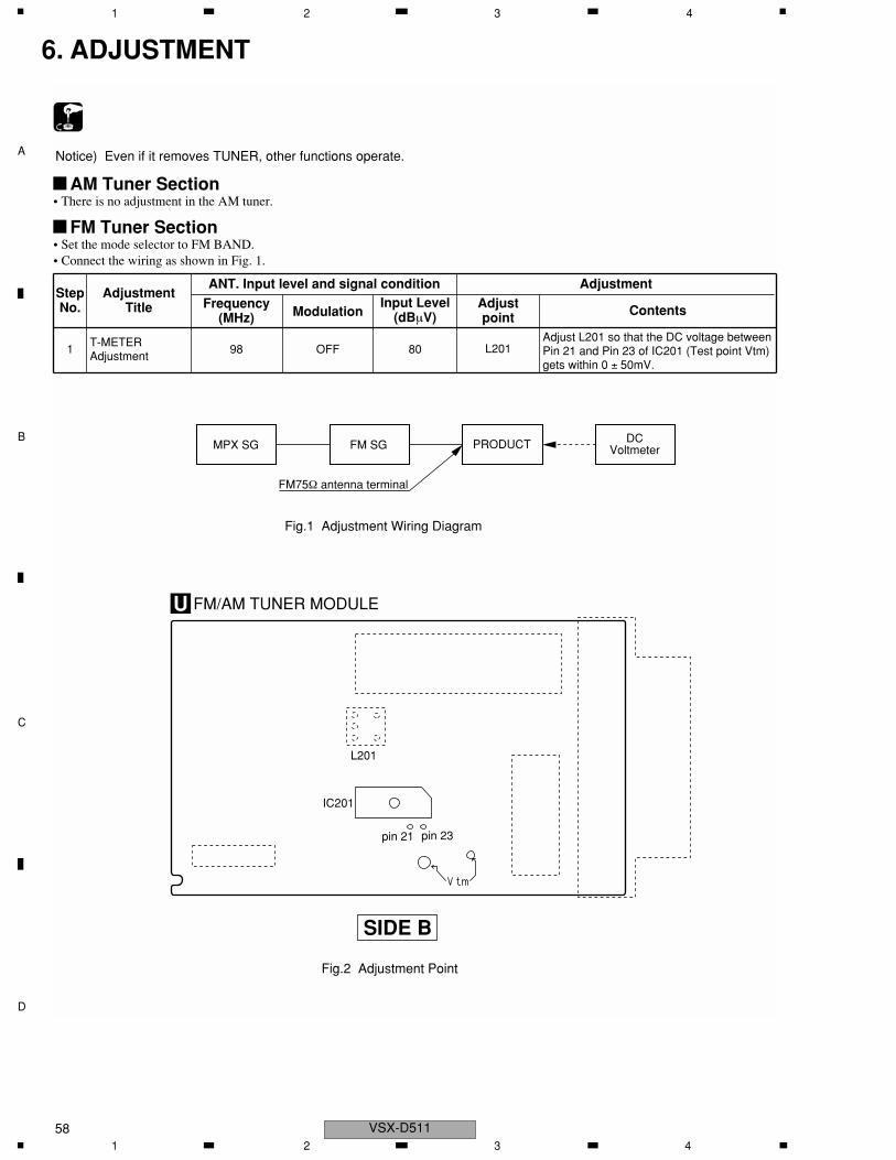
6. ADJUSTMENT
MPX SG FM SG PRODUCT DCVoltmeter
L201
IC201
pin 21 pin 23
FM/AM TUNER MODULEU
SIDE B
StepNo.
AdjustmentTitle
ANT. Input level and signal condition AdjustmentInput Level
(dBµV)Adjustpoint ContentsFrequency
(MHz) Modulation
1T-METER Adjustment
98 OFF 80 L201Adjust L201 so that the DC voltage between Pin 21 and Pin 23 of IC201 (Test point Vtm) gets within 0 ± 50mV.
AM Tuner Section• There is no adjustment in the AM tuner.
FM75Ω antenna terminal
Fig.1 Adjustment Wiring Diagram
Notice) Even if it removes TUNER, other functions operate.
Fig.2 Adjustment Point
FM Tuner Section• Set the mode selector to FM BAND.• Connect the wiring as shown in Fig. 1.
1 2 3 4

A
B
C
D
5 6 7 8
VSX-D511
7. GENERAL INFORMATION7.1 DISASSEMBLY and DIAGNOSI
2 ×2
Remove the Bonnet (seven screws).1
Rear PanelPull up
2
2
4
Diagnosis
AMP&PRIMARY AssyREGULATOR Assy
Heat Sink
5
×22 ×3
2 ×5
3 ×3
×2
2 ×3
Disassembly
PCB Location
AMP&PRIMARY Assy
FRONT Assy
AMP INPUT Assy
D.D & INPUT Assy
VIDEO Assy
FM/AM TUNER Unit
6CH IN Assy
POWER SW Assy
TRANS 3 Assy
TRANS 2 Assy
TRANS 1 Assy
R. ENCODER Assy
NOTE : This photograph is VSX-D711
P
HA
KAWA Assy KL
DIGITAL IN Assy JM
OQ
DICB
REGULATOR AssyE
H.P. AssyU
Note : This photograph shows other models. However, the work method is the same.
Note : If a speaker and the screw of a rear panel are removed, a set will stop moving. Even if it removes TUNER Unit, it is uninfluential in operation of those other than TUNER Unit.
7.1.1 DISASSEMBLY and PCB LOCATION
5 6 7 859

A
B
C
D
1 2 3 4
VSX-D51160
IC 5001: Expand ICBU4094BCF TUNER MODULE
2: Serial InIC 9504
3: CLK SYS CK SYS CLK SYS CLKROM FOR
IC9502: FLIP/FLOP1: ST EXP ST SYS DATA SYS DATA
DD/DTSIC9503: FLIP/FLOP
15: OE EXP OE TUNED TUNEDPD8097A(MR27V802D) TC74VHC574F
IC 301: Expand IC STEREO STEREOBU4094BCF PLL CE PLL CE
2: Serial In SYS DT PLL DO PLL DO10: Q 3: CLK SYS CK T MUTE T MUTE
1: ST EXP ST15: OE EXP OE OE CLK CLK
IC101: Function SelectorTC9273F-007
15: DATA SYS DT14: CLK SYS CK
16: ST 9273STST
IC103: EVOL (6-CH)M62446FP
40: DATA SYS DT41: CLK SYS CK CE OE
39: LATCH EVRST SDI1~4SDTO
IC9101: CODEC SDI1~3 BICK IC 9501: Main DSPAK4586VQ SDTO LRCK CS493292
BICKLRCK
IC9601:NJU7313AM
17: DATA SYS DT16: CLK SYS CK
14: ST SYS ST
IC102: Function SelectorNJU7312AM
17: DATA SYS DT 5V/3V Level Shifter16: CLK SYS CK IC9505: 5V -->3V TC74LVX244FT
14: ST SYS ST IC9506: 3V-->5V TC74VHCT244AFT
96kCDTO
CRSTPLL DO CCSPLL CS IC401: CCKTUNED System Microprocessor CDTSTEREO CSDOTMUTE
PDG268BCRES
RDS DATARDS CLK
SC
DO
UT
INT
RE
Q
SC
DIN
SC
CLK
CS
RE
SE
T
CK
CS
DO
PD
N
DI ER
R
CO
CS
CO
DO
CO
PD
FS
96
ER
R
EV
RS
T
EX
P O
E
9273ST
ST
CO
CK
SY
S D
T
SY
S C
K
SY
S S
T
59ST
K
A
A
A
A
A
A
A
A
U
A A
A
O
7.1.2 U-COM BLOCKDIAGRAM
1 2 3 4

A
B
C
D
5 6 7 8
VSX-D511
1. DC abnormal detection
7.1.3 PROTECTION CIRCUIT
It processes more preferentially than overload detection.
*A.MUTE : Audio mute command
↓
An unusual state continues for 3 seconds.
↓ continuation ↓ return
A power supply is shut off. A program is performed from the
beginning.
↓
The power key cannot be effective for 60 seconds
If the AC plug is pulled off within 60 sec, and then it is plugged in again, the unit will be reset for 60 se
2. Overload detection
↓
An unusual state continues for 3 seconds.
↓ continuation ↓ return
A power supply is shut off. A power supply is shut off even if it
returns.
When detected DC abnormal, A.MUTE* is on
and speaker relay is off, then flash
"AMP_ERR" on display.
When detected overload, A.MUTE* is on and
speaker relay is off, then flash
"OVERLOAD" on display.
5 6 7 861

A
B
C
D
1 2 3 4
VSX-D51162
020
040
010
0012
0014
0018
0028
0030
0036
0048
0052
00 (
mse
c)
AC
rel
ay"H
"
(on
)
"L"
(
mut
e)
(por
t)
A.M
UT
E"L
"or"
H"
(por
t)
FU
NC
TIO
N S
Wfu
ll op
enla
st d
ata
(TC
9273
F)
IC10
1
DS
P,2c
h, 5
.1ch
LIN
Efu
ll op
enla
st d
ata
(NJU
7313
AM
) IC
9601
VID
EO
sys
tem
mut
e(of
f)la
st d
ata
(NJM
2296
) IC
301
IC35
1/IC
352
TU
NE
Rdu
mm
y da
tala
st d
ata
(LC
7213
1) IC
202
E-V
OLU
ME
mut
ela
st d
ata
(M62
446F
P)
IC10
3
DS
Pre
set
star
t con
trol
(CS
4932
9) IC
9501
DIR
/CO
DE
Cre
set
star
t con
trol
(AK
4586
) IC
9101
SP
EK
ER
rel
ayof
fon
OV
ER
LOA
D D
ET
EC
Tst
art c
ontr
ol
AM
P E
RR
OR
DE
TE
CT
star
t con
trol
A
A
A A ALN
U
PO
WE
R O
N S
EQ
UE
NC
E7.1.4 POWER ON SEQUENCE
1 2 3 4

A
B
C
D
5 6 7 8
VSX-D511
0 200 400
AC relay "H" "L"
(port)
A.MUTE "L"
(port)
FUNCTION SW full open
(TC9273F) IC101
DSP,2ch, 5.1ch LINE full open
(NJU7313AM) IC9601
VIDEO system mute
(NJM2296) IC301IC351/IC352
TUNER mute
(LC72131) IC202
E-VOLUME mute
(M62446FP) IC103
DSP
(CS49329) IC9501
DIR/CODEC
(AK4586) IC9101
SPEKER relay on off
(port)
OVERLOAD DETECT
AMP ERROR DETECT
A
A
A
A
A
LN
U
POWER OFF SEQUENCE
7.1.5 POWER OFF SEQUENCE
5 6 7 863

A
B
C
D
1 2 3 4
VSX-D51164
7.2 PARTS7.2.1 IC
7 Pin Arrangement (Top View)
7 PDG268A (FRONT ASSY : IC401)• System Control MCU
• The information shown in the list is basic information and may not correspond exactly to that shown in the schematic diagrams.
• List of ICPDG268A, AK4586VQ, BD3812F, NJU7312AM, PD8097A, AK4382
1G2
G1
NC
ACIN
RDS_DT
RDS_CK
OVFB
RMC
VER_2
PLL_CE
CDC_CS
CDC_CK
CDC_DO
CDC_DI
STEREO
TUNED
VENC_A
VENC_B
A.MUTE
CSB
DSP_CS
DSP_CK
DSP_SI
DSP_SO
MVOL_ATT
ST_EVR
PLL_DO
KEYIN1
KEYIN2
G1/A1
G0/A0
NC
PE0/EC0/INT0
PE1/EC1/INT1
PE2/INT2
PE3/INT3/NMI
PE4/RMC
PE5
PE6/PWM
PE7/TO/ADJ
PC0/KR0
PC1/KR1
PC2/KR2
PC3/KR3
PC4/KR4
PC5/KR5
PC6/KR6
PC7/KR7
PB0/CINT
PB1/CS0
PB2/SCK0
PB3/SI0
PB4/SO0
PB5/SCK1
PB6/SI1
PB7/SO1
AVREF
PA1/AN0
PA1/AN1
KE
YIN
3
VE
R_1
FE
NC
_A
FE
NC
_B
AM
P_D
C
AM
P_O
L
9459
_ST
MV
RA
TT
SY
S_C
K
SY
S_D
T
PA
2/A
N2
PA
3/A
N3
PA
4/A
N4
PA
5/A
N5
PA
6/A
N6
PA
7/A
N7
AV
SS
RS
T
EX
TA
L
XT
AL
VS
S
TX
TE
X
VD
D
VF
IP
PD
0/A
55
PD
1/A
54
PD
2/A
53
PD
3/A
52
PD
4/A
51
A21
A22
A23
PH7/A24
PH6/A25
PH5/A26
PH4/A27
PH3/A28
PH2/A29
PH1/A30
PH0/A31
PG7/A32
PG6/A33
PG5/A34
PG4/A35
PG3/A36
PG2/A37
PG1/A38
PG0/A39
PF7/A40
PF6/A41
PF5/A42
PF4/A43
PF3/A44
PF2/A45
PF1/A46
PF0/A47
PD7/A48
PD6/A49
PD5/A50
S11
S12
S13
S14
S15
S16
S17
S18
S19
S20
S21
S22
4053INH
4053A
RY_B
RY_C/R
RY_A
RY_AC
GAIN_SEL
NECK_SEL
DSP_RST
9164_CS
T_MUTE
T_POWON
NC
FM+(RDS)
CDC_RST
DSP_MT
9273_CS
D_MUTE
G2/
A2
G3/
A3
G4/
A4
G5/
A5
G6/
A6
G7/
A7
G8/
A8
G9/
A9
G10
/A10
G11
/A11
G12
/A12
VD
D
G13
/A13
G14
/A14
G15
/A15
A16
A17
A18
A19
A20
G3
G4
G5
G6
G7
G8
G9
G10
NC
S1
S2
S3
S4
S5
S6
S7
S8
S9
S10
2
3
4
5
6
7
8
9
10
11
12
13
14
15
16
17
18
19
20
100
99 98 97 96 95 94 93 92 91 90 89 88 87 86 85 84 83 82 81
31 32 33 34 35 36 37 38 39 40 41 42 43 44 45 46 47 48 49 50
21
22
23
24
25
26
27
28
29
30
80
79
78
77
76
75
74
73
72
71
70
69
68
67
66
65
64
63
62
61
60
59
58
57
56
55
54
53
52
51
1 2 3 4
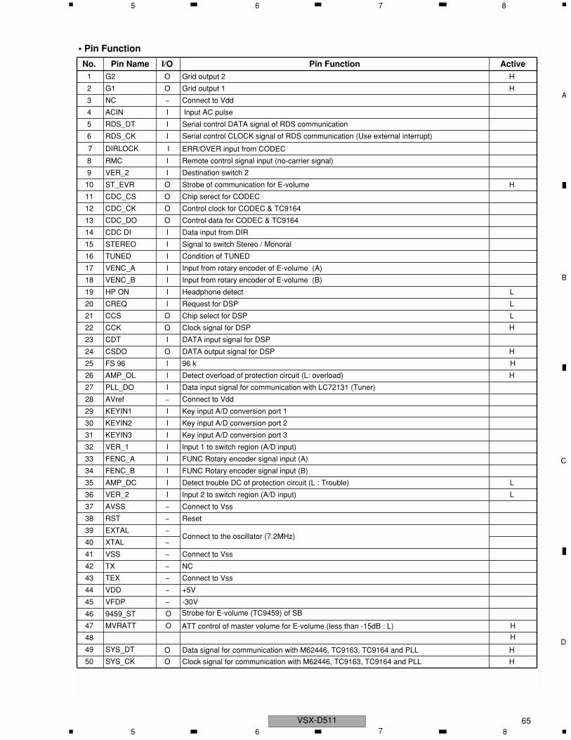
A
B
C
D
5 6 7 8
VSX-D511
• Pin Function
No. Pin Name I/O Pin Function Active1 G2 O Grid output 2 H
2 G1 O Grid output 1 H
3 NC − Connect to Vdd
4 ACIN I lnput AC pulse
5 RDS_DT I Serial control DATA signal of RDS communication
6 RDS_CK I Serial control CLOCK signal of RDS communication (Use external interrupt)
7 DIRLOCK I ERR/OVER input from CODEC
8 RMC I Remote control signal input (no-carrier signal)
9 VER_2 I Destination switch 2
10 ST_EVR O Strobe of communication for E-volume H
11 CDC_CS O Chip serect for CODEC
12 CDC_CK O Control clock for CODEC & TC9164
13 CDC_DO O Control data for CODEC & TC9164
14 CDC DI I Data input from DIR
15 STEREO I Signal to switch Stereo / Monoral
16 TUNED I Condition of TUNED
17 VENC_A I Input from rotary encoder of E-volume (A)
18 VENC_B I Input from rotary encoder of E-volume (B)
19 HP ON I Headphone detect L
20 CREQ l Request for DSP L
21 CCS O Chip select for DSP L
22 CCK O Clock signal for DSP H
23 CDT I DATA input signal for DSP
24 CSDO O DATA output signal for DSP H
25 FS 96 l 96 k H
26 AMP_OL l Detect overload of protection circuit (L: overload) H
27 PLL_DO I Data input signal for communication with LC72131 (Tuner)
28 AVref − Connect to Vdd
29 KEYIN1 I Key input A/D conversion port 1
30 KEYIN2 I Key input A/D conversion port 2
31 KEYIN3 I Key input A/D conversion port 3
32 VER_1 I lnput 1 to switch region (A/D input)
33 FENC_A I FUNC Rotary encoder signal input (A)
34 FENC_B I FUNC Rotary encoder signal input (B)
35 AMP_DC I Detect trouble DC of protection circuit (L : Trouble) L
36 VER_2 I lnput 2 to switch region (A/D input) L
37 AVSS − Connect to Vss
38 RST − Reset
39 EXTAL −Connect to the oscillator (7.2MHz)
40 XTAL −
41 VSS − Connect to Vss
42 TX − NC
43 TEX − Connect to Vss
44 VDD − +5V
45 VFDP − -30V
46 9459_ST
O
O Strobe for E-volume (TC9459) of SB
ATT control of master volume for E-volume (less than -15dB : L) H
H
47 MVRATT
48
49 SYS_DT O Data signal for communication with M62446, TC9163, TC9164 and PLL H
O Clock signal for communication with M62446, TC9163, TC9164 and PLL H50 SYS_CK
5 6 7 865
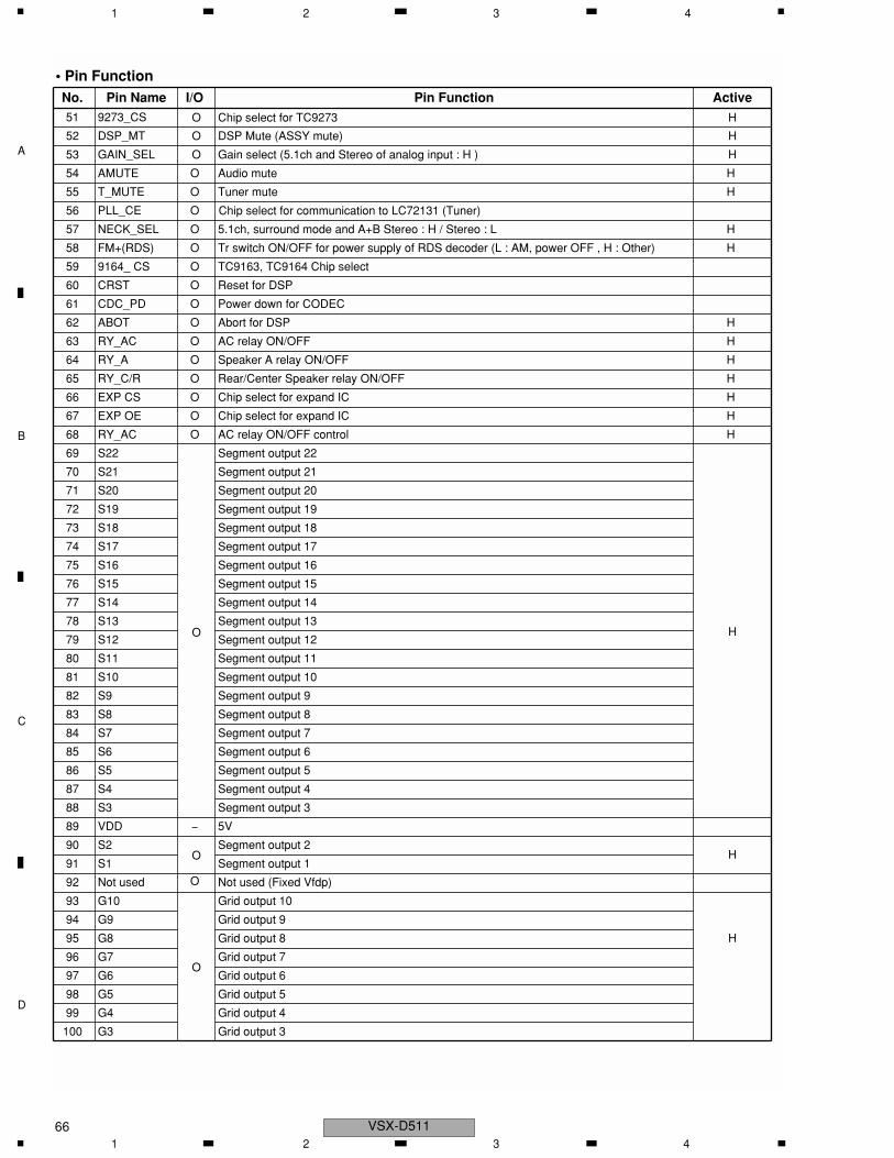
A
B
C
D
1 2 3 4
VSX-D51166
• Pin FunctionNo. Pin Name I/O Pin Function Active51 9273_CS
O DSP Mute (ASSY mute)
O Chip select for TC9273
O Gain select (5.1ch and Stereo of analog input : H )
H
H
H
52 DSP_MT
53 GAIN_SEL
54 AMUTE O Audio mute H
55 T_MUTE O Tuner mute H
56 PLL_CE O
57 NECK_SEL O 5.1ch, surround mode and A+B Stereo : H / Stereo : L H
58 FM+(RDS) O Tr switch ON/OFF for power supply of RDS decoder (L : AM, power OFF , H : Other) H
59 9164_ CS O TC9163, TC9164 Chip select
60 CRST O Reset for DSP
61 CDC_PD O Power down for CODEC
62 ABOT O Abort for DSP H
63 RY_AC O AC relay ON/OFF H
64 RY_A O Speaker A relay ON/OFF H
65 RY_C/R O Rear/Center Speaker relay ON/OFF H
66 EXP CS O Chip select for expand IC H
67 EXP OE O Chip select for expand IC H
68 RY_AC O
O
AC relay ON/OFF control H
69 S22
O
Segment output 22
H
70 S21 Segment output 21
71 S20 Segment output 20
72 S19 Segment output 19
73 S18 Segment output 18
74 S17 Segment output 17
75 S16 Segment output 16
76 S15 Segment output 15
77 S14 Segment output 14
78 S13 Segment output 13
79 S12 Segment output 12
80 S11 Segment output 11
81 S10 Segment output 10
82 S9 Segment output 9
H
83 S8 Segment output 8
84 S7 Segment output 7
85 S6 Segment output 6
86 S5 Segment output 5
87 S4 Segment output 4
88 S3 Segment output 3
89 VDD − 5V
90 S2
O
OSegment output 2
H
91 S1 Segment output 1
92 Not used Not used (Fixed Vfdp)
93 G10 Grid output 10
94 G9 Grid output 9
95 G8 Grid output 8
96 G7 Grid output 7
97 G6 Grid output 6
98 G5 Grid output 5
99 G4 Grid output 4
100 G3 Grid output 3
Chip select for communication to LC72131 (Tuner)
1 2 3 4

A
B
C
D
5 6 7 8
VSX-D511
7 Pin Arrangement (Top View)
7 Block Diagram
7 AK4586VQ (DD & INPUT ASSY : IC9101)• 96kHz 24Bit 6-channel CODEC with DIR
5 6 7 867

A
B
C
D
1 2 3 4
VSX-D51168
7 Pin / Function
1 2 3 4

A
B
C
D
5 6 7 8
VSX-D511
7 Pin / Function
5 6 7 869
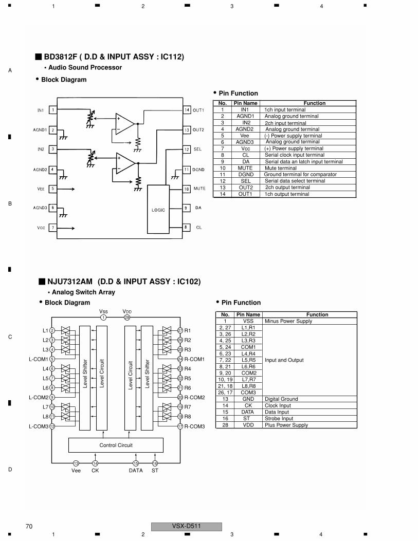
A
B
C
D
1 2 3 4
VSX-D51170
• Pin FunctionNo. Pin Name Function1 IN1 1ch input terminal2 AGND1 Analog ground terminal3 IN24 AGND25 Vee6 AGND37 Vcc8 CL
2ch input terminal
9 DA10 MUTE11 DGND12 SEL13 OUT214 OUT1
• Pin Function
No. Pin Name Function1 VSS Minus Power Supply
2, 27 L1,R13, 26 L2,R24, 25 L3,R35, 24 COM16, 23 L4,R47, 22 L5,R5 Input and Output8, 21 L6,R69, 20 COM210, 19 L7,R721, 18 L8,R826, 17 COM3
13 GND Digital
Plus Power Supply
Ground14 CK Clock Input15 DATA Data Input16 ST Strobe Input28 VDD
Analog ground terminal(-) Power supply terminalAnalog ground terminal(+) Power supply terminalSerial clock input terminalSerial data an latch input terminalMute terminalGround terminal for comparatorSerial data select terminal2ch output terminal1ch output terminal
VDDVss
L1
281
CKVee
1413
STDATA
1615
2
L2 3
L3 4
L-COM1
Leve
l Shi
fter
Leve
l Shi
fter
Leve
l Circ
uit
Leve
l Circ
uit5
L4 6
L5 7
L6 8
L-COM2 9
L7 10
Control Circuit
L8 11
L-COM3
R1
R2
R3
R-COM1
R4
R5
R6
R-COM2
R7
R8
R-COM312
27
26
25
24
23
22
21
20
19
18
17
NJU7312AM (D.D & INPUT ASSY : IC102) • Analog Switch Array
• Block Diagram
Block Diagram
BD3812F ( D.D & INPUT ASSY : IC112) • Audio Sound Processor
•
1 2 3 4

A
B
C
D
5 6 7 8
VSX-D511
7 Pin Arrangement (Top View)
7 Block Diagram
7 PD8097A (D.D & INPUT ASSY : IC9504)
• 4Mb P2ROM
5 6 7 871
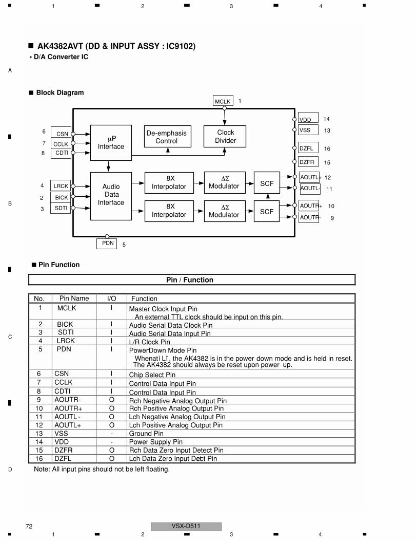
A
B
C
D
1 2 3 4
VSX-D51172
7 Pin Function
1
2
3
4
5
6
7
816
15
14
13
12
11
10
9
7 Block Diagram
Pin / Function
No. Pin Name I/O Function 1 MCLK I Master Clock Input Pin
An external TTL clock should be input on this pin. 2 BICK I Audio Serial Data Clock Pin 3 SDTI I Audio Serial Data Input Pin 4 LRCK I L/R Clock Pin 5 PDN I Power-Down Mode Pin
When at ì Lî , the AK4382 is in the power- down mode and is held in reset. The AK4382 should always be reset upon power- up.
6 CSN I Chip Select Pin 7 CCLK I Control Data Input Pin 8 CDTI I Control Data Input Pin 9 AOUTR- O Rch Negative Analog Output Pin 10 AOUTR+ O Rch Positive Analog Output Pin 11 AOUTL - O Lch Negative Analog Output Pin 12 AOUTL+ O Lch Positive Analog Output Pin 13 VSS - Ground Pin 14 VDD - Power Supply Pin 15 DZFR O Rch Data Zero Input Detect Pin 16 DZFL O Lch Data Zero Input Detect Pin
Note: All input pins should not be left floating.
LRCK
BICK
SDTI
AudioData
Interface
MCLK
PDN
∆ΣModulator
AOUTL+8XInterpolator SCF
AOUTR+SCF
VDD
VSSDe-emphasisControlµP
Interface
ClockDivider
CSN
CCLK
CDTI
DZFR
∆ΣModulator
8XInterpolator
AOUTL-
AOUTR-
DZFL
7 AK4382AVT (DD & INPUT ASSY : IC9102)• D/A Converter IC
1 2 3 4

A
B
C
D
5 6 7 8
VSX-D511
7.2.2 DISPLAY
• Pin Assignment
• Grid Assignment
• Segment Designation
(1G)(9G to 2G)
n ce
Dp1
Dp2
pr
d1 d2
m
k bf
g
jh
S1S2 S3 S4
a2a1
ce
d
bfg
a
49 1
1G10G
9G 8G 7G 6G 5G 4G 3G 2G
7 XAV3013 (FRONT ASSY : V401)• FL DISPLAY
dB
SIGNAL AUTO SB MIDNIGHT
LOUDNESS
DIRECT MONITORSTEREO TUNEDMONOANALOG DTS MPEG
DIGITAL ADV.SURR. NEO:6
DIGITAL PRO LOGIC ∏
ATT
MPEG
RF ATT EON
SP £ AB
dB
SIGNAL AUTO SB
MIDNIGHTLOUDNESS
DIRECT MONITORTUNED
MONOANALOG DTS MPEGSTEREO DIGITAL
DIGITAL PRO LOGIC∏
ATTRe-EQMPEGADV.SURR.
RF ATT EONRDS
Neo:6DIGITAL
SP ‰ AB
DIGITAL Re-EQ RDS
5 6 7 873

A
B
C
D
1 2 3 4
VSX-D51174
Pin No. 26 2549 48 47 46 45 44 43 42 41 40 39 38 37 36 35 34 33 32 31 30 29 28 27
Connection F2 F2 NP NP P22 P21 P20 P19 P18 P17 P16 P15 P14 P13 P12 P11 P10 P9 P8 P7 P6 P5 P4 P3 P2
Pin No. 24 23 22 21 20 19 18 17 16 15 14 13 12 11 10 9 8 7 6 5 4 3 2 1
Connection P1 NX NX NX NX NX NX NX NX NX 10G 9G 8G 7G 6G 5G 4G 3G 2G 1G NP NP F1 F1
• Pin Connection
• Anode Connection
NOTE 1) F1, F2.......... Filament2) NP................ No pin3) NX................ No extend pin4) DL................. Datum Line5) 1G to 10G..... Grid6) Field of vision is a minimum of 21.8° from the lower side.
2GP1P2P3P4P5P6P7P8P9P10P11P12P13P14P15P16P17P18P19P20P21P22
a2
a1
S3
h
j
k
b
f
mg
c
e
r
pn
d1
d2
Dp2
Dp1S1
S4
S2
10G 9G
a2
a1
S3
h
j
k
b
f
mg
c
e
r
pn
d1
d2
Dp2
Dp1S1
S4
S2
8G
a2
a1
S3
h
j
k
b
f
mg
c
e
r
pn
d1
d2
Dp2
Dp1S1
S4
S2
7G
a2
a1
S3
h
j
k
b
f
mg
c
e
r
pn
d1
d2
Dp2
Dp1S1
S4
S2
6G
a2
a1
S3
h
j
k
b
f
mg
c
e
r
pn
d1
d2
Dp2
Dp1S1
S4
S2
5G
a2
a1
S3
h
j
k
b
f
mg
c
e
r
pn
d1
d2
Dp2
Dp1S1
S4
S2
4G
a2
a1
S3
h
j
k
b
f
mg
c
e
r
pn
d1
d2
Dp2
Dp1S1
S4
S2
3G
a2
a1
S3
h
j
k
b
f
mg
c
e
r
pn
d1
d2
Dp2
Dp1S1
S4
S2
1G
EON
√
TUNED
RDS
S1
A
B1a
1b
1f
1g
1c1e
1d
RFATT
MONO
DTS
MPEG
ANALOG
2e
S1
DIRECT
MIDNIGHT
AUTO
SB
MONITOR
PROLOGIC ∏
DIGITAL (L)
Neo:6
2f
MPEG
2g
2b
2d
DIGITAL
DIGITAL (R)
ATT
ADV.SURR.
Re-EQ
LOUDNESS
STEREO
2c
2a
1 2 3 4

A
B
C
D
5 6 7 8
VSX-D511
8. PANEL FACILITIES
DOWN
STATION
TUNER EDIT INPUT ATT FL DIMMERCLASS BAND MPX
STANDARDADVANCEDSURROUND
STEREO/DIRECT
SIGNALSELECT
UP
ENTER
INPUTSELECTOR
MASTER VOLUME
MULTI JOG
AUDIO/VIDEO MULTI-CHANNEL RECEIVER
R
STANDBY
STANDBY/ON
PHONES
TUNING MONITOR
MULTI JOG
MULTI JOG
MIDNIGHT LOUDNESS TONE QUICK SETUP
LISTENING MODE
N∫m-Û.,,
31 2 4
17 18 19 20108 9 11 12 13 14 15 16 21
6 75
22
1 STANDBY/ON
Switches the receiver between on and standby.
2 STANDBY indicatorLights when the receiver is in standby mode.
3 STATION (+/–) buttons Selects station presets when using the tuner.
4 TUNING (+/–) buttons
5 Remote sensorReceives the signals from the remote control.
6 ENTER
8 PHONES jack Use to connect headphones.
9 TUNER EDIT Press to memorize and name a station for recall using the station (+/-) buttons.
10 CLASS Switches between the three banks (classes) of station presets.
11 BAND Switches between AM and FM radio bands.
12 MPX Press the MPX button to receive a radio broadcast in mono.
Selects the frequency when using the tuner.
7 MULTI JOG/INPUT SELECTOR dial
The MULTI JOG/INPUT SELECTOR dial performs a number of tasks. Use it to select options after pressing TONE CONTROL, QUICK SETUP or TUNER EDIT.
When the headphones are connected, there is no sound output from the speakers.
13 INPUT ATT Use to attenuate (lower) the level of an analog input signal to prevent distortion.
14 FL DIMMER Use this button to make the fluorescent display (FL) dimmer or brighter.
15 LISTENING MODE buttons STANDARD Press for Standard decoding and to switch between the various Pro Logic II options.ADVANCED SURROUND Use to switch between the various surround modes.
STEREO/DIRECT Switches direct playback on or off. Direct playback bypasses the tone controls and channel levels for the most accurate reproduction of a source.
16 SIGNAL SELECT Use to select between an analog or digital signal.
17 MONITOR Press to switch tape monitoring on/off.
18 MIDNIGHT Use when listening to movie soundtracks at low volumes.
19 LOUDNESS Use to boost the bass and treble at low volumes.
20 TONE Press this button to access the bass and treble controls,
which you can then adjust with the MULTI JOG/INPUT SELECTOR dial.
21 QUICK SETUP22 MASTER VOLUME
Front panel
5 6 7 875

A
B
C
D
1 2 3 4
VSX-D51176
1 2 3 4 5 6 7 8 9
10 131211 14
Display
1 SIGNAL SELECT indicatorsLights to indicate the type of input signal assigned for the currentcomponent:
AUTOLights when AUTO signal select is on
SB Depending on the source, this lights when a signal withsurround back channel encoding is detected.
DIGITALLights when a digital audio signal is detected.
2 DIGITALLights when a Dolby Digital encoded signal is detected.
ANALOGLights when an analog signal is detected.
DTSLights when a source with DTS encoded audio signals isdetected.
2 DTSWhen the Standard mode of the receiver is on, this lights to indicatedecoding of a DTS signal.
3 2 DIGITALWhen the Standard mode of the receiver is on, this lights to indicatedecoding of a Dolby Digital signal.
4 2 PRO LOGIC IIWhen the Standard mode of the receiver is on, this lights to indicatePro Logic II decoding.
5 ATTLights when INPUT ATT is used to attenuate (reduce) the level ofthe analog input signal.
6 DIRECTLights when source direct playback is in use. This functionbypasses all tone, balance, Advanced surround, and DolbySurround effects.
7 MIDNIGHTLights during Midnight listening.
8 MONITORLights when MONITOR is selected
9 Speaker indicatorShows the speaker system currently in use.
10 Character display
11 ADV. SURR (Advanced Surround)Lights when one of the Advanced Surround modes has beenselected.
12 LOUDNESSLights when LOUDNESS has been selected.
13 TUNER indicators
STEREO:Lights when a stereo FM broadcast is being received in auto stereomode.
MONO:Lights when the mono mode is set using the
MPX button.
TUNED:Lights when a broadcast is being received.
14 Master volume levelShows the overall volume level. ---dB indicates the minimum level,and −0 dB indicates the maximum level.
Depending on your level settings for each channel, the maximumlevel can range between –10 dB and –0 dB.
1 2 3 4

A
B
C
D
5 6 7 8
VSX-D511
Remote control
1 RECEIVER Switches the receiver between on and standby.
2 MIDNIGHT/LOUDNESSUse to switch to Midnight or Loudness listening.
3 LISTENING MODE buttons STANDARD Press for Standard decoding and to switch between the various Pro Logic II options.
ADVANCED SURROUND Use to switch between the various surround modes.
STEREO/DIRECT (pages 24–25) Switches direct playback on or off. Direct playback bypasses the tone controls and channel levels for the most accurate reproduction of a source.
4 INPUT ATTUse to attenuate (lower) the level of an analog input signal to prevent distortion.
5 FL DIMMER Use this button to make the fluorescent display (FL) dimmer or brighter.
6 MENU (DVD control)Use to access different menus associated with your DVD player. TUNER EDIT (Receiver control) (pages 35–36)Press to memorize and name a station for recall using the STATION (+/–) buttons.
7 DVD Use to switch over to the DVD controls on the remote control.
The DVD controls on the remote control (TOP MENU, MENU, ] ’ ‘ and ENTER/SETUP buttons) can only be used for DVD control after pressing DVD on the remote. See the next page for more on the seperate DVD CONTROL buttons.
8 INPUT SELECTOR buttonsUse to select the input source. 9 Volume buttonsUse MASTER VOLUME +/– to set the overall listening volume. Use MUTE to mute the sound or restore the sound if it has been muted.
10 Tuner controlsThe TUNING +/– buttons can be used to find radio frequencies. The STATION +/– buttons can be used to select preset radio stations.
BAND Use to switch between the AM and FM bands when the tuner is selected.
CLASS Use to switch between the three banks
(classes) of station presets.
MPX Use to switch between auto stereo and mono
reception of FM broadcasts. If the signal is weak then switching to mono will improve the sound quality.
DISPLAY Use to switch the display between the station preset name
and the frequency.
11 TOP MENUDisplays the disc ‘top’ menu of a DVD.
12 ] ’ ‘ and ENTER/SETUP buttons Use these arrow buttons when setting up your surround sound system. These buttons are also used to control DVD menus/options.
INPUT SELECTORCDTV/SATDVD/LDRECEIVER
DVD
DVD CONTROL
SUB TITLE
AUDIOTESTTONE LEVEL EFFECT
MENU
DVD
TUNEREDIT
RECEI-VER
TOP MENU
STANDARD STEREOADVANCEDSURROUND
INPUTATT
FLDIMMER MUTE
MASTERVOLUME
CD-R/TAPE/MD
VCR/DVR
ENTER
SETUP
AV RECEIVER
TUNING
BAND CLASS MPX DISPLAY
CH SELECT
STATION
MIDNIGHT/LOUDNESS TUNER
Î
1
¢4
¡
7 8
3
2
6
7
1
345
11
12
13
10
15
14
9
8
5 6 7 877
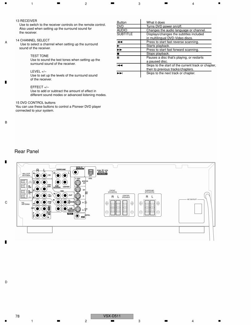
A
B
C
D
1 2 3 4
VSX-D51178
MONITOROUT
OUT
IN
IN
IN
S - VIDEO
VCR /DVR
T V /SAT
DVD /LD
CONTROLOUT
AMLOOP
FMUNBAL75Ω
PREOUT
VIDEO
ASSIGNABLEDIGITAL IN
Rear Panel
AM LOOPANTENNA
FM ANTENNA
LR
LRR L
SURROUNDSPEAKERS
CENTERSPEAKER
AC OUTLETLR
FRONTSPEAKERS
TOMONTORTV
VCR /DVR
CDIN
IN
INOUT
OUT
CD - R/ TAPE
/ MD
SURROUND
CENTERSUBWOOFER
SUBWOOFERPREOUT
IN
IN
IN
IN
TV /SAT
DVD/ LD
OPT
(CD)
PLAY
PCM / / DTSDIGITAL INASSIGNABLE
13 RECEIVER Use to switch to the receiver controls on the remote control. Also used when setting up the surround sound for the receiver.
14 CHANNEL SELECT Use to select a channel when setting up the surround sound of the receiver.
TEST TONE Use to sound the test tones when setting up the
surround sound of the receiver.
LEVEL +/– Use to set up the levels of the surround sound
of the receiver.
EFFECT +/– Use to add or subtract the amount of effect in
different sound modes or advanced listening modes.
15 DVD CONTROL buttonsYou can use these buttons to control a Pioneer DVD player connected to your system.
Button What it doesDVD Turns DVD power on/off.AUDIO Changes the audio language or channel.SUBTITLE Displays/changes the subtitles included
in multilingual DVD-Video discs.1 Press to start fast reverse scanning. 3 Starts playback.¡ Press to start fast forward scanning. 7 Stops playback.8 Pauses a disc that’s playing, or restarts
a paused disc.4 Skips to the start of the current track or chapter,
then to previous tracks/chapters.¢ Skips to the next track or chapter.
1 2 3 4
Related Documents