International Journal of Engineering Research and Development e-ISSN: 2278-067X, p-ISSN: 2278-800X, www.ijerd.com Volume 10, Issue 12 (December 2014), PP.46-57 46 VSC BASED HVDC SYTEM DESIGN AND PROTECTION AGAINST OVER VOLTAGES Ch.Yaswanth 1 , A.Vijayasri 2 1 PG scholar, Department of Electrical and Electronics Engineering, P.V.P .Siddhartha Institute of Technology, Vijayawada-520007, 2 Assistant professor, Department of Electrical and Electronics Engineering, P.V.P. Siddhartha Institute of Technology, Vijayawada-520007, Abstract:- High Voltage Direct Current system based on voltage source converter (VSC-HVDC) is becoming more effective solution for offshore wind plants and supplying power to remote regions. In this paper, the control of a VSC-based HVDC system (VSC-HVDC) is described. Based on this control strategy, appropriate controllers utilizing PI controllers are designed to control the active and reactive power at each end station.The operation performance of a voltage source converter (VSC) based HVDC (VSC-HVDC system) system is explained under some characteristic faulted conditions with and without protection measures. A protection strategy is proposed to enhance the continuous operation performance of the VSC-HVDC system. The strategy utilizes a voltage chopper to suppress over-voltages on the DC side of the VSC. Digital simulation is done to verify the validity of the proposed control strategy and protection strategy. Index Terms:- Voltage source converter, VSC-HVDC system, Control strategies, Faults, Protection I. INTRODUCTION High Voltage Direct Current (HVDC) transmission is a high power electronics technology used in electric power systems for power transmission over very long distances. For many years HVDC based on thyristor commutated converters was used. With the development of semiconductors and control equipment HVDC transmission with voltage source converters (VSC) based on IGBT are used. HVDC transmission based on VSC uses pulse width modulation with relatively high switching frequencies which makes it possible to generate ac output voltage with any desired phase angle or amplitude instantly. VSC converter topology can rapidly control both active and reactive power independently of one another [3]. Reactive power can also be controlled at each terminal independent of the dc transmission voltage level. The dynamic support of the ac voltage at each converter terminal improves the voltage stability and increase the transfer capability of the sending end receiving end ac system. For continuous operation, the VSC-HVDC system should supply as much electric power as possible during faults. Controls must be adjusted to provide the optimized response over the range of normal system operation, transient, and faulted conditions. The reliable operation of a VSC-HVDC system requires that at any time the circuit elements should not exceed its ratings. The protection is used to suppress over-voltage. In this paper a proper control of the VSC-HVDC system is described in detail [5]-[7]. The protection strategy study and its performance verification are carried out on the base of simulation results obtained by MATLAB for different operation conditions. II. SYSTEM DISCRIPTION A Typical VSC-HVDC System is shown in the fig1.the HVDC link itself constituted by two VSCs connected either back to back or through a dc cable, depending on the application. The VSC is three phase three level twelve pulse bridges, employing IGBT power semiconductors [8]. The converters are connected to phase reactors, which are connected to conventional transformers. The reactors are used for controlling the active and reactive power by regulating the currents through them and for reducing the high frequency harmonic content of the ac line current caused by the switching of the VSCs. Tuned shunt filters are used to reduce high frequency ripple on the ac voltage and current. The transformers reduce the ac system voltage to a value suitable for converters. The dc capacitors provide a low inductance path for the turn-off current and energy storage to be able to control the power flow [2]-[4]. Capacitors are also used to reduce the voltage ripple on the dc side. Polymeric cables are preferred for HVDC.

VSC BASED HVDC SYTEM DESIGN AND PROTECTION AGAINST OVER VOLTAGES
Jul 13, 2015
Welcome message from author
This document is posted to help you gain knowledge. Please leave a comment to let me know what you think about it! Share it to your friends and learn new things together.
Transcript

International Journal of Engineering Research and Development
e-ISSN: 2278-067X, p-ISSN: 2278-800X, www.ijerd.com
Volume 10, Issue 12 (December 2014), PP.46-57
46
VSC BASED HVDC SYTEM DESIGN AND PROTECTION
AGAINST OVER VOLTAGES
Ch.Yaswanth1, A.Vijayasri
2
1PG scholar, Department of Electrical and Electronics Engineering, P.V.P .Siddhartha Institute of Technology,
Vijayawada-520007, 2Assistant professor, Department of Electrical and Electronics Engineering, P.V.P. Siddhartha Institute of
Technology, Vijayawada-520007,
Abstract:- High Voltage Direct Current system based on voltage source converter (VSC-HVDC) is becoming
more effective solution for offshore wind plants and supplying power to remote regions. In this paper, the
control of a VSC-based HVDC system (VSC-HVDC) is described. Based on this control strategy, appropriate
controllers utilizing PI controllers are designed to control the active and reactive power at each end station.The
operation performance of a voltage source converter (VSC) based HVDC (VSC-HVDC system) system is
explained under some characteristic faulted conditions with and without protection measures. A protection
strategy is proposed to enhance the continuous operation performance of the VSC-HVDC system. The strategy
utilizes a voltage chopper to suppress over-voltages on the DC side of the VSC. Digital simulation is done to
verify the validity of the proposed control strategy and protection strategy.
Index Terms:- Voltage source converter, VSC-HVDC system, Control strategies, Faults, Protection
I. INTRODUCTION High Voltage Direct Current (HVDC) transmission is a high power electronics technology used in
electric power systems for power transmission over very long distances. For many years HVDC based on
thyristor commutated converters was used. With the development of semiconductors and control equipment
HVDC transmission with voltage source converters (VSC) based on IGBT are used.
HVDC transmission based on VSC uses pulse width modulation with relatively high switching
frequencies which makes it possible to generate ac output voltage with any desired phase angle or amplitude
instantly. VSC converter topology can rapidly control both active and reactive power independently of one
another [3]. Reactive power can also be controlled at each terminal independent of the dc transmission voltage
level. The dynamic support of the ac voltage at each converter terminal improves the voltage stability and
increase the transfer capability of the sending end receiving end ac system.
For continuous operation, the VSC-HVDC system should supply as much electric power as possible
during faults. Controls must be adjusted to provide the optimized response over the range of normal system
operation, transient, and faulted conditions. The reliable operation of a VSC-HVDC system requires that at any
time the circuit elements should not exceed its ratings. The protection is used to suppress over-voltage.
In this paper a proper control of the VSC-HVDC system is described in detail [5]-[7]. The protection
strategy study and its performance verification are carried out on the base of simulation results obtained by
MATLAB for different operation conditions.
II. SYSTEM DISCRIPTION A Typical VSC-HVDC System is shown in the fig1.the HVDC link itself constituted by two VSCs
connected either back to back or through a dc cable, depending on the application. The VSC is three phase three
level twelve pulse bridges, employing IGBT power semiconductors [8]. The converters are connected to phase
reactors, which are connected to conventional transformers. The reactors are used for controlling the active and
reactive power by regulating the currents through them and for reducing the high frequency harmonic content of
the ac line current caused by the switching of the VSCs. Tuned shunt filters are used to reduce high frequency
ripple on the ac voltage and current. The transformers reduce the ac system voltage to a value suitable for
converters. The dc capacitors provide a low inductance path for the turn-off current and energy storage to be
able to control the power flow [2]-[4]. Capacitors are also used to reduce the voltage ripple on the dc side.
Polymeric cables are preferred for HVDC.

VSC BASED HVDC SYTEM DESIGN AND PROTECTION AGAINST OVER VOLTAGES
47
Fig.1: Configuration of VSC-HVDC.
III. CONTROL SYSTEM The control system of the VSC-HVDC is based on the fast inner current control loop controlling the ac
current. The ac current references are supplied by the outer controllers. The outer controller includes the dc
voltage controller, active power controller, reactive power controller, frequency controller [5]-[9]. The reference
value of the active current is derived from the dc voltage controller, active power controller. The reference value
of the reactive current is derived from the ac voltage controller, reactive power controller. In all these controllers
integrators are used to eliminate the steady state errors. In these one converter control the dc voltage to achieve
the power balance [13][14]. The other converter can set any active power value within the limits for the system.
Fig. 2: Control system of VSC-HVDC.
A.INNERCURRENTCONTROLLER
The inner current control loop is implemented in the dq-frame. The objectives of the inner current
controller are to track the current reference values given by the outer controllers and to generate the voltage
reference values i.e. and fed to controlled voltage source.
From fig. 2. The quantities at the ac side of the converter are related by
(1)
Rewriting in Laplace domain leads to
(2)
Transforming to the dq-components results in
(3)
(4)
Where V is the common bus voltage, L is the leakage inductance of the phase reactor, i is the current flowing at
the ac side of the converter, U is the voltage generated by the converter, S is the Laplace operator, is the d
axis component of the common bus voltage, is the q axis component of the common bus voltage, is the q-
axis component of current flowing at the ac side of the converter, is the q-axis component of current flowing at
the ac side of the converter, is the d-axis component of the voltage generated by the converter, is the q-axis
component of the voltage generated by the converter.

VSC BASED HVDC SYTEM DESIGN AND PROTECTION AGAINST OVER VOLTAGES
48
The speed voltage terms , introduces cross coupling between d axis quantities and q axis
quantities. This cross coupling makes controlling of the reactive power independently to the active power
difficult. In order to eliminate the cross coupling, and are feed forward on the d-axis controller while
and are feed forward on q- axis controller [7]. The inner current controller is shown in the fig.3.
Fig.3: Inner current controller.
B.OUTER CONTROLLERS
1) DC VOLTAGE CONTROL:
The instantaneous active power and reactive power transmitted in the three-phase system and the
power transmitted on the dc side of the VSC are expressed in dq frame is
(5)
(6)
(7)
Neglecting the losses in the phase reactor and converter, equating the power on the dc and ac sides of the
converter using the above equations (5) and (7)
(8)
Any unbalance between ac and dc power leads to change in voltage over the dc link Capacitor
(9)
Where, is the current through the dc cable
By integrating between and and dividing by , assuming that the average value of and are
constant during the interval and that the dc voltage tracks the reference equation is
(10)
Substituting the equation (8) in (10)
(11)
Finally from the control equation for the current reference is
(12)
Where ,
2) ACTIVE POWER CONTROLLER:
A simple method to control the active power is open loop control [8]. The active current reference is
obtained as
(13)
Where, p is the desired active power.
If more accurate control is needed then a feedback loop and an open loop is used.
VSC BASED HVDC SYTEM DESIGN AND PROTECTION AGAINST OVER VOLTAGES
49
3) REACTIVE POWER CONTROLLER:
A simple method to control the reactive power is open loop control [8]. The reactive power reference is
obtained as
(14)
Where, q is the desired reactive power.
If more accurate control is needed then a feedback loop and an open loop control is used.
IV. SIMULATION STUDY To test the response of the designed control system, the system shown in the fig1 is simulated by using
MATLAB SIMULINK software. All the simulation has been performed with three level converters. The
converter bridge values are represented as ideal switches. On state losses and switching losses are neglected
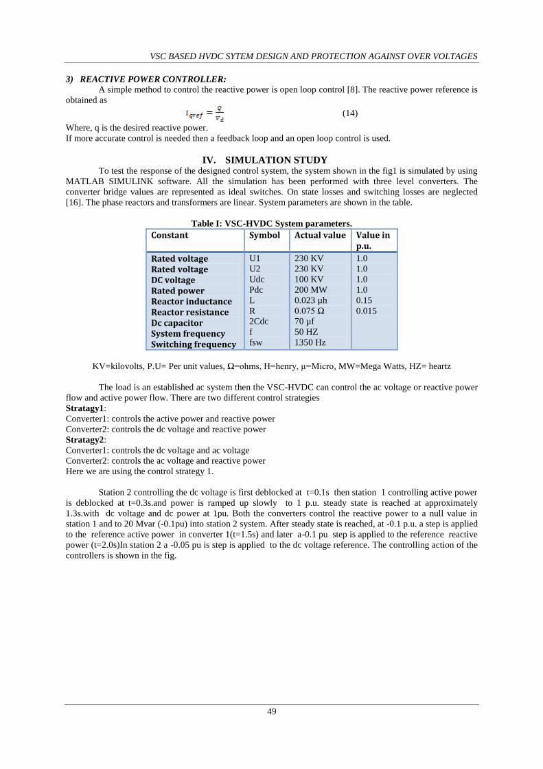
[16]. The phase reactors and transformers are linear. System parameters are shown in the table.
Table I: VSC-HVDC System parameters.
Constant Symbol Actual value Value in p.u.
Rated voltage Rated voltage DC voltage Rated power Reactor inductance Reactor resistance Dc capacitor System frequency Switching frequency
U1
U2
Udc
Pdc
L
R
2Cdc
f
fsw
230 KV
230 KV
100 KV
200 MW
0.023 µh
0.075 Ω
70 µf
50 HZ
1350 Hz
1.0
1.0
1.0
1.0
0.15
0.015
KV=kilovolts, P.U= Per unit values, Ω=ohms, H=henry, µ=Micro, MW=Mega Watts, HZ= heartz
The load is an established ac system then the VSC-HVDC can control the ac voltage or reactive power
flow and active power flow. There are two different control strategies
Stratagy1:
Converter1: controls the active power and reactive power
Converter2: controls the dc voltage and reactive power
Stratagy2:
Converter1: controls the dc voltage and ac voltage
Converter2: controls the ac voltage and reactive power
Here we are using the control strategy 1.
Station 2 controlling the dc voltage is first deblocked at t=0.1s then station 1 controlling active power
is deblocked at t=0.3s.and power is ramped up slowly to 1 p.u. steady state is reached at approximately
1.3s.with dc voltage and dc power at 1pu. Both the converters control the reactive power to a null value in
station 1 and to 20 Mvar (-0.1pu) into station 2 system. After steady state is reached, at -0.1 p.u. a step is applied
to the reference active power in converter 1(t=1.5s) and later a-0.1 pu step is applied to the reference reactive
power (t=2.0s)In station 2 a -0.05 pu is step is applied to the dc voltage reference. The controlling action of the
controllers is shown in the fig.

VSC BASED HVDC SYTEM DESIGN AND PROTECTION AGAINST OVER VOLTAGES
50
V. SIMULATION RESULTS
Fig.4: DC voltage, DC power at sending end.
Fig.5: Three phase Ac voltage, three phase Ac current at sending end.
Fig.6: DC voltage,DC power at receving end.
Fig.7: Three phase Ac voltage, three phase Ac current at the receiving end.
.

VSC BASED HVDC SYTEM DESIGN AND PROTECTION AGAINST OVER VOLTAGES
51
Fig.8: Active power, Reactive power due to step change in input at sending end.
Fig.9: Dc voltage,Reactive power due to step change in input at receiving end.
VI. FAULT ANALYSIS A. Single line to ground fault at the sending end side:
A single phase fault is made in phase A at the receiving end side at 2.1sec and is cleared at 2.5sec. The
voltage at the faulted phase a in receiving end side decreases from1 p.u. to ground and recovers to normal value
after clearing fault. The voltages in the sending end side are not affected by the unbalanced voltage at the
receiving end side. The phase currents at fault side increases and at the other side there is small decrease in
value [5]. The active power and reactive power at the faulted side decreases and recovers to normal value after
clearing the fault. As the corresponding active power and reactive power at the sending end is constant about
small oscillations at the beginning and ending of the fault. Due to ac side fault the power that can inject into the
ac system is decreased. This will cause the dc capacitors will charge then the dc voltage at the receiving end side
and sending end side increases during the fault and recovers to normal value after clearing the fault. The
increased DC voltage at the receiving end side and sending end side are shown in the fig 10&11.
B. Phase to phase fault at the receiving end side:
A phase to phase fault is simulated between phase A and phase B at the receiving end side ac network
at 2.1sec and is cleared at 2.5sec. The phase voltages at receiving end side it is observed that the voltage in
phase c is not effected by the fault while the voltages in phase a and b are reduced. The dc voltage ripple appears
during the fault, which is bigger than the dc voltage ripple produced by the single line to ground fault [5]. The
active power in the receiving end side decreases due to decrease in voltage but as in the sending end side active
and reactive power are maintained constant about a small oscillations during the fault period the side also. The
current values at the receiving side are increased and in sending end side they are decreased. The increased DC
voltage at the receiving end side and sending end side are shown in the fig12&13.

VSC BASED HVDC SYTEM DESIGN AND PROTECTION AGAINST OVER VOLTAGES
52
C. Phase to phase to ground fault at the receiving end side:
Another case is simulated when phase a and b are grounded at the receiving end side at 2.1sec and is
cleared at 2.5sec. The phase voltages at the receiving end side it is observed that that the voltages in phase a and
b reduces to ground due to ground fault. The dc voltage is raised and power is decreased due to decrease in the
ac system voltage [5]. As the fault in phase to phase to ground is severe fault when compared to single line to
ground fault and double line to ground fault. The increased DC voltage at the receiving end side and sending
end side are shown in the fig14&15.
D. Three phase to ground fault at the receiving end side:
A three phase to ground fault is simulated at the receiving end side at 2.1sec and is cleared at 2.5sec.
The voltage at the sending end side is maintained to 1 p.u except small oscillations during the fault. The ac
voltage at the receiving end side is reduced during fault and recovers fast and successfully to the reference value
after clearing the fault. The real power flow is reduced to very low during the fault and recovers to normal value
after clearing the fault. The phase currents at receiving end side increases and have over current transients at the
beginning and ending of the fault. From the simulation it can be observed that during a three phase fault the
decreased voltages at converter terminals strongly reduce the power flow by the dc link. When the fault is
cleared normal operation is recovered fast.so the severity of the three phase fault is more when compared to the
unbalanced faults. For all these faults the change in the values of the HVDC system are tabulated. The increased
DC voltage at the receiving end side and sending end side are shown in the fig16&17.
Table II: Fault analysis at receiving end.
Type of fault
Udc (p.u)
Pdc (p.u)
Pmeas (p.u)
Qmeas (p.u)
Umeas (p.u)
Uabc (p.u)
SLGF 1.4 0.8 0.7 oscillates 0.7 Va=0
LLF 2 0.6 0.4 oscillates 0.6 Va=vb
LLGF 2.5 0.5 0.2 oscillates 0.3 Va=vb=0
LLLGF 3 0.3 0 0 0 Va=vb=vc=0
P.U= per unit values
Table III: Fault analysis at sending end
Type of fault
Udc (p.u)
Pdc (p.u)
Pmeas (p.u)
Qmeas (p.u)
Umeas (p.u)
Uabc (p.u)
SLGF 1.4 0.8 Small Transients Small Transient Constant Constant
LLF 2 0.6 Small Transients oscillates Constant Small Transients
LLGF 2.5 0.5 Small Transients oscillates Constant Small Transient
LLLGF 3 0.3 Small Transients oscillates Constant Small Transient
P.U= per unit values.
Fig.10: Single line to ground fault at the sending end.

VSC BASED HVDC SYTEM DESIGN AND PROTECTION AGAINST OVER VOLTAGES
53
Fig.11. Single line to ground fault at the receiving end.
Fig.12: Double line fault at the sending end.
Fig.13: Double line fault at the receiving end.
Fig.14: Double line to ground fault at sending end.

VSC BASED HVDC SYTEM DESIGN AND PROTECTION AGAINST OVER VOLTAGES
54
Fig.15: Double line to ground fault at receiving end.
Fig.16: Three phase fault at sending end.
Fig.17: Three phase fault at receiving end.
VII. PROTECTION AGAINST OVER VOLTAGE To overcome the over-voltage problem, a voltage chopper with a fast switch IGBT and a resistor in
series, can be Provided in parallel to the DC capacitor bank. The chopper can be used to discharge the capacitor
banks in a controlled manner and to reduce the DC voltage to a suitable value. For example, as soon as the
voltage Udl exceeds its upper limit value, the switch Tcl will be triggered on, then the capacitors will be
discharged through resister and Tcl, thus Udl decreases. On the time of Udl decreases to its lower limit value,
Tcl will be triggered off. Therefore, Udl can never exceed its permitted upper limit value [16].
A. Operation performance of VSC-HVDC system with proposed protection strategy Under Faulted condition
The simulation results corresponding to the characteristic fault cases are shown in below figs. from
which we can conclude that the magnitude of the DC voltage during fault conditions are greatly decreased,
while compared with the results in the same fault condition with protection.

VSC BASED HVDC SYTEM DESIGN AND PROTECTION AGAINST OVER VOLTAGES
55
Fig.18: Single line to ground fault at sending end.
Fig.19: Single line to ground fault at the receiving end.
Fig.20: Double line fault at the sending end.
Fig.21: Double line to ground fault at receiving end.

VSC BASED HVDC SYTEM DESIGN AND PROTECTION AGAINST OVER VOLTAGES
56
Fig.22: Double line to ground fault at sending end.
Fig.23: Double line to ground fault at receiving end.
Fig.24: Three phase fault at the sending end.
Fig.25: Three phase fault at the receiving end.

VSC BASED HVDC SYTEM DESIGN AND PROTECTION AGAINST OVER VOLTAGES
57
VIII. CONCLUSION This paper presents the performance of VSC based HVDC system under normal and fault conditions
with and without protection strategies. The modeling and controlling of HVDC system with three level VSC are
discussed. From the simulation results it is conclude that the system performance is fast .High quality ac
currents, ac voltages are obtained. The active power and the reactive power can be controlled independently and
are bi-directional. During the faults the performance of the VSC-HVDC system analyzed. From this analysis we observe
that the three phase fault is severe when compared to the unbalanced faults. DC voltage choppers are used to
suppress the over-voltages on the dc side of VSC-HVDC.
REFERENCES [1]. Schettler F., Huang H., and Christl N. "HVDC transmission systems using voltage source converters –
design and applications," IEEE Power Engineering Society Summer Meeting, July 2000.
[2]. Du, C. and E. Agneholm. Investigation of Frequency/Ac voltage control for inverter station of VSC-
HVDC. in Proc. 32nd IEEE Annual Conference on Industrial Electronics. 2007. Paris, France.
[3]. Bajracharaya, C., "Control of VSC-HVDC for wind power", M.Sc. thesis, Norwegian University of
Science and Technology, June 2008.
[4]. Lie Xu, Andersen B. R.; Cartwright P., Control of VSC transmission systems under unbalanced
network conditions, Transmission and Distribution Conference and Exposition, 7-12 Sept, 2003 IEEE
PES, 2003, 2, pp. 626-632.
[5]. Modelling, Control design and Analysis of VSC based HVDC Transmission Systems. R. Padiyar and
Nagesh Prabhu, 2004 international Conference on Power System Technology - POWERCON 2004
Singapore, 21-24 November 2004.
[6]. C. Du, A. Sannino, and M. H. J. Bollen, “Analysis of the control algorithms of voltage-source converter
HVDC,” accepted to IEEE Powertech 2005.
[7]. Hongtao Liu, Zheng Xu, Zhi Gao. A Control Strategy for Three-level VSC-HVDC system System
Proceedings of IEEE PES Summer Meeting2002. Chicago, USA, July.21-25,2002
[8]. K. Suzuki, T. Nakajima, H. Konishi, T. Nakamura, "A Study of Control System for Self-Commutated
Convener Compensator”. LEE Japan, Vol.] 12-B No. I. Jan., 1992.
[9]. Lindberg, Anders "PWM and control of two and three level high power voltage source converters,"
Licentiate thesis, ISSN-1100-1615, TRITA-EHE 9501, The Royal Institute of Technology, Sweden,
1995.
[10]. R. Ruder all, J. Charpentier, and R. Sharma, High voltage direct current (HVDC) transmission systems
technology review paper, in Energy Week, Washington, D.C, USA, Mar. 2000.
[11]. Harnefors, L. Control of VSC-HVDC Transmissions. in Proc. 2008 IEEE Power Electronics Specialists
Conference. 2008. Rhodes, Greece.
[12]. U. Axelsson, A. Holm, C. Liljegren, and K. Eriksson, Gotland HVDC Light transmission-world first
commercial small scale dc transmission, in CIRED Conference, Nice, France, May 1999.
[13]. A Edstrom, “High power electronics HVDC and SVC”, Electric Power Research Center, Stockholm,
Sweden.
[14]. J. Arrillaga, High Voltage Direct Current Transmission. London: The Institution of Electrical
Engineers, 1998.
[15]. D. F.Menzies, J. Graham, and F. U. Ribeiro, Garabi the Argentina-Brazil 1000MW interconnection
commissioning and early operating experience, in ERLAC Conference, Foz do Iguacu, Brazil, May-
June 2001.
[16]. T. Larsson, A. Edris, D. Kidd, and F. Aboytes, Eagle Pass back-to-back tie: a dual purpose application
of voltage source converter technology, in Proc. of IEEE Power Engineering Society Summer Meeting,
vol. 3, July 2001, pp. 1686 – 1691.
[17]. Hongtao Liu, Hangzhou, Zheng Xu , Ying Huang” study of protection strategy for vsc based hvdc
system” Transmission and Distribution Conference and Exposition, 2003 IEEE PES .
Related Documents