VR5500 High voltage PMIC with multiple SMPS and LDO Rev. 6 — 29 January 2020 Product data sheet 1 General description The VR5500 is an automotive high-voltage multi-output power supply integrated circuit, with focus on Radio, V2X, and Infotainment applications. It includes multiple switch mode and linear voltage regulators. It offers external frequency synchronization input and output, for optimized system EMC performance and it is qualified in compliance with AEC-Q100 rev H (Grade1, MSL3). Several device versions are available, offering choice in number of output rails, output voltage setting, operating frequency, and power up sequencing, to address multiple applications. 2 Features and benefits • 60 V DC maximum input voltage for 12 V and 24 V applications • VPRE synchronous buck controller with external MOSFETs. Configurable output voltage, switching frequency, and current capability up to 10 A peak. • Low voltage integrated synchronous BUCK1 converter, dedicated to MCU core supply with SVS capability. Configurable output voltage and current capability up to 3.6 A peak. • Low voltage integrated synchronous BUCK2 converter. Configurable output voltage and current capability up to 3.6 A peak. Multi-phase capability with BUCK1 to extend the current capability up to 7.2 A peak on a single rail. Static voltage scaling capability. • Low voltage integrated synchronous BUCK3 converter. Configurable output voltage and current capability up to 3.6 A peak. • BOOST converter with integrated low-side switch. Configurable output voltage and max input current up to 1.5 A peak. • EMC optimization techniques including SMPS frequency synchronization, spread spectrum, slew rate control, manual frequency tuning • Two linear voltage regulators for MCU IOs and ADC supply, external physical layer. Configurable output voltage and current capability up to 400 mA DC. • OFF mode with very low sleep current (10 μA typ) • Two input pins for wake-up detection and battery voltage sensing • Device control via I2C interface with CRC • Power synchronization pin to operate two VR5500 devices or VR5500 plus an external PMIC • Three voltage monitoring circuits, dedicated interface for MCU monitoring, power good, reset, and interrupt outputs • Configuration by OTP programming. Prototype enablement to support custom setting during project development in engineering mode.

Welcome message from author
This document is posted to help you gain knowledge. Please leave a comment to let me know what you think about it! Share it to your friends and learn new things together.
Transcript

VR5500High voltage PMIC with multiple SMPS and LDORev. 6 — 29 January 2020 Product data sheet
1 General description
The VR5500 is an automotive high-voltage multi-output power supply integrated circuit,with focus on Radio, V2X, and Infotainment applications. It includes multiple switchmode and linear voltage regulators. It offers external frequency synchronization inputand output, for optimized system EMC performance and it is qualified in compliance withAEC-Q100 rev H (Grade1, MSL3).
Several device versions are available, offering choice in number of output rails, outputvoltage setting, operating frequency, and power up sequencing, to address multipleapplications.
2 Features and benefits
• 60 V DC maximum input voltage for 12 V and 24 V applications• VPRE synchronous buck controller with external MOSFETs. Configurable output
voltage, switching frequency, and current capability up to 10 A peak.• Low voltage integrated synchronous BUCK1 converter, dedicated to MCU core supply
with SVS capability. Configurable output voltage and current capability up to 3.6 Apeak.
• Low voltage integrated synchronous BUCK2 converter. Configurable output voltageand current capability up to 3.6 A peak. Multi-phase capability with BUCK1 to extendthe current capability up to 7.2 A peak on a single rail. Static voltage scaling capability.
• Low voltage integrated synchronous BUCK3 converter. Configurable output voltageand current capability up to 3.6 A peak.
• BOOST converter with integrated low-side switch. Configurable output voltage and maxinput current up to 1.5 A peak.
• EMC optimization techniques including SMPS frequency synchronization, spreadspectrum, slew rate control, manual frequency tuning
• Two linear voltage regulators for MCU IOs and ADC supply, external physical layer.Configurable output voltage and current capability up to 400 mA DC.
• OFF mode with very low sleep current (10 μA typ)• Two input pins for wake-up detection and battery voltage sensing• Device control via I2C interface with CRC• Power synchronization pin to operate two VR5500 devices or VR5500 plus an external
PMIC• Three voltage monitoring circuits, dedicated interface for MCU monitoring, power good,
reset, and interrupt outputs• Configuration by OTP programming. Prototype enablement to support custom setting
during project development in engineering mode.
NXP Semiconductors VR5500High voltage PMIC with multiple SMPS and LDO
VR5500 All information provided in this document is subject to legal disclaimers. © NXP B.V. 2020. All rights reserved.
Product data sheet Rev. 6 — 29 January 20202 / 131
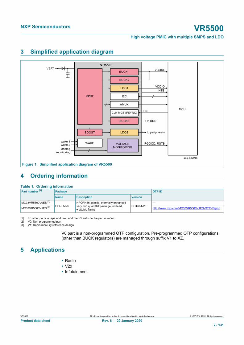
3 Simplified application diagram
aaa-032945
VBATVR5500
BUCK1
BUCK2
BUCK3 to DDR
to peripherals
LDO1
LDO2
VCORE
VDDIOINTB
I2C
AMUX
CLK MGT (FSYNC)
VPRE
MCU
WAKEwake 1wake 2analog
monitoring
BOOST
VOLTAGEMONITORING
PGOOD, RSTB
FIN
Figure 1. Simplified application diagram of VR5500
4 Ordering informationTable 1. Ordering information
PackagePart number [1]
Name Description Version
OTP ID
MC33VR5500V0ES [2] —
MC33VR5500V1ES [3] HPQFN56HPQFN56, plastic, thermally enhancedvery thin quad flat package, no lead,wettable flanks
SOT684-23http://www.nxp.com/MC33VR5500V1ES-OTP-Report
[1] To order parts in tape and reel, add the R2 suffix to the part number.[2] V0: Non-programmed part[3] V1: Radio mercury reference design
V0 part is a non-programmed OTP configuration. Pre-programmed OTP configurations(other than BUCK regulators) are managed through suffix V1 to XZ.
5 Applications
• Radio• V2x• Infotainment

NXP Semiconductors VR5500High voltage PMIC with multiple SMPS and LDO
VR5500 All information provided in this document is subject to legal disclaimers. © NXP B.V. 2020. All rights reserved.
Product data sheet Rev. 6 — 29 January 20203 / 131
6 Block diagram
aaa-032946
CLK_MGT
BIASCONTROL
POWER MANAGEMENTSTATE MACHINE
ANALOGMUX
PGOODDRIVERVOLTAGE
SUPERVISION
VMON1
VDDIO
RESETDRIVER
VR5500
IN (s) VDDIO
AMUX
BUCK3
ILIMTSD GB1 BUCK3-SWBUCK3-FBBUCK3-INQBUCK3-IN
VPRECONTROLLER
ILIM
FIN/Bias
GB1PRE_GLSPRE_BOOT
PRE_SW
PRE_GHS
VDDIO
VCOREMON
VMON1
SCLSDA
VDDI2C
WAKE2WAKE1
LDO1
LDO1_IN
DBG
FIN
PGOOD
RSTB
FOUT
INTBPSYNC
OSC
I2C
WAKE
VSUP
ePAD
Vdig
OTP
BUCK2
ILIMTSD GB1LDO1
ILIMTSD GB1
LDO2
VBOOST
LDO2
ILIMTSD GB1
BOOST_LS BOOST
VBOS BOS
ILIMTSD GB1
BUCK2-SWBUCK2-FBBUCK2-IN
ePAD
BUCK1
ILIMTSD GB1BUCK1-SWBUCK1-FBBUCK1-IN
ePAD
ePAD
GND VSUP1/2 PRE_CSPPRE_COMP PRE_FB
Figure 2. Block diagram of VR5500

NXP Semiconductors VR5500High voltage PMIC with multiple SMPS and LDO
VR5500 All information provided in this document is subject to legal disclaimers. © NXP B.V. 2020. All rights reserved.
Product data sheet Rev. 6 — 29 January 20204 / 131
7 Pinning information
7.1 Pinning
aaa-032947
LDO
1_IN
56
LDO
155
LDO
254
VBO
OST
53
n.c.
52
VSU
P251
VSU
P150
WAK
E149
PRE_
FB48
VBO
S47
PRE_
BOO
T46
PRE_
GH
S45
PRE_
SW44
PRE_
GLS
43
PRE_CSP42
PRE_COMP41
n.c.40
BUCK1_FB39
PSYNC38
BUCK1_SW37
BUCK1_IN36
BUCK2_IN35
BUCK2_SW34
INTB33
BUCK2_FB32
n.c.31
n.c.30
AMUX29
n.c.
15
VMO
N1
16
VCO
REM
ON
17
PGO
OD
18
RST
B19
FIN
20
GN
D21
GN
D22
VDD
IO23
FOU
T24
n.c.
25
n.c.
26
n.c.
27
n.c.
28
WAKE2 1
n.c. 2
BUCK3_INQ 3
VDDI2C 4
BOOT_LS 5
BUCK3_IN 6
BUCK3_SWEXPOSED PAD
7
DBG 8
BUCK3_FB 9
SCL 10
SDA 11
n.c. 12
n.c. 13
n.c. 14
Figure 3. Pin configuration for HVQFN56
7.2 Pin descriptionSee Section 8 for connection of unused pins.
Table 2. Pin descriptionSymbol Pin Type Description
WAKE2 1 A_IN / D_IN Wake-up input 2An external serial resistor is required if WAKE2 is a global pin
n.c. 2 n.c. Not connected pin
BUCK3_INQ 3 A_IN Low voltage Buck3 quiet input voltage
VDDI2C 4 A_IN Input voltage for I2C buffers
BOOST_LS 5 A_IN Boost low-side drain of internal MOSFET
BUCK3_IN 6 A_IN Low voltage Buck3 input voltage
BUCK3_SW 7 A_OUT Low voltage Buck3 switching node
DBG 8 A_IN Debug mode entry
BUCK3_FB 9 A_IN Low voltage Buck3 voltage feedback
NXP Semiconductors VR5500High voltage PMIC with multiple SMPS and LDO
VR5500 All information provided in this document is subject to legal disclaimers. © NXP B.V. 2020. All rights reserved.
Product data sheet Rev. 6 — 29 January 20205 / 131
Symbol Pin Type Description
SCL 10 D_IN I2C-busClock input
SDA 11 D_IN/OUT I2C-busBidirectional data line
n.c. 12 n.c. Not connected pin
n.c. 13 n.c. Not connected pin
n.c. 14 n.c. Not connected pin
n.c. 15 n.c. Not connected pin
VMON1 16 A_IN Voltage monitoring input 1
VCOREMON 17 A_IN VCORE monitoring input: Must be connected to Buck1 outputvoltage
PGOOD 18 D_OUT Power good outputActive lowPull up to VDDIO mandatory
RSTB 19 D_OUT Reset outputActive lowThe main function is to reset the MCU. Reset input voltage ismonitored to detect external reset and fault condition.Pull up to VDDIO mandatory
FIN 20 D_IN Frequency synchronization input
GND 21 GND Ground
GND 22 GND Ground
VDDIO 23 A_IN Input voltage FOUT and AMUX buffersAllow voltage compatibility with MCU I/Os
FOUT 24 D_OUT Frequency synchronization output
n.c. 25 n.c. Not connected pin
n.c. 26 n.c. Not connected pin
n.c. 27 GND External pull down to GND
n.c. 28 n.c. Not connected pin
AMUX 29 A_OUT Multiplexed output to connect to MCU ADCSelection of the analog parameter through I2C
n.c. 30 n.c. Not connected pin
n.c. 31 n.c. Not connected pin
BUCK2_FB 32 A_IN Low voltage Buck2 voltage feedback
INTB 33 D_OUT Interrupt output
BUCK2_SW 34 A_OUT Low voltage Buck2 switching node
BUCK2_IN 35 A_IN Low voltage Buck2 input voltage
BUCK1_IN 36 A_IN Low voltage Buck1 input voltage
BUCK1_SW 37 A_OUT Low voltage Buck1 switching node
PSYNC 38 D_IN/OUT Power synchronization input/output
BUCK1_FB 39 A_IN Low voltage Buck1 voltage feedback
n.c. 40 GND External pull down to GND
PRE_COMP 41 A_IN VPRE compensation network
PRE_CSP 42 A_IN VPRE positive current sense input
NXP Semiconductors VR5500High voltage PMIC with multiple SMPS and LDO
VR5500 All information provided in this document is subject to legal disclaimers. © NXP B.V. 2020. All rights reserved.
Product data sheet Rev. 6 — 29 January 20206 / 131
Symbol Pin Type Description
PRE_GLS 43 A_OUT VPRE low-side gate driver for external MOSFET
PRE_SW 44 A_OUT VPRE switching node
PRE_GHS 45 A_OUT VPRE high-side gate driver for external MOSFET
PRE_BOOT 46 A_IN/OUT VPRE bootstrap capacitor
VBOS 47 A_OUT Best of supply output voltage
PRE_FB 48 A_IN VPRE voltage feedback and negative current sense input
WAKE1 49 A_IN / D_IN Wake up input 1An external serial resistor is required if WAKE1 is a global pin
VSUP1 50 A_IN Power supply 1 of the deviceAn external reverse battery protection diode in series ismandatory
VSUP2 51 A_IN Power supply 2 of the deviceAn external reverse battery protection diode in series ismandatory
n.c. 52 n.c. Not connected pin
VBOOST 53 A_IN VBOOST voltage feedback
LDO2 54 A_OUT Linear regulator 2 output voltage
LDO1 55 A_OUT Linear regulator 1 output voltage
LDO1_IN 56 A_IN Linear regulator 1 input voltage
EP 57 GND Exposed pad (BUCK1, BUCK2 and BUCK3 low-side GNDsare connected to the expose pad)Must be connected to GND
8 Connection of unused pinsTable 3. Connection of unused pinsPin Name Type Connection if not used
1 WAKE2 A_IN / D_IN External pull down to GND
2 n.c. n.c. Open
3 BUCK3_INQ A_IN Open
4 VDDI2C A_IN Open
5 BOOST_LS A_IN See Section 21.5 "VBOOST not populated"
6 BUCK3_IN A_IN Open
7 BUCK3_SW A_OUT Open
8 DBG A_IN Connection mandatory
9 BUCK3_FB A_IN Open – 1.5 MΩ internal resistor bridge pull down to GND
10 SCL D_IN External pull down to GND
11 SDA D_IN/OUT External pull down to GND
12 n.c. n.c. Open
13 n.c. n.c. Open
14 n.c. n.c. Open
15 n.c. n.c. Open
16 VMON1 A_IN Open – 2 MΩ internal pull down to GND, OTP_VMON1_EN=0

NXP Semiconductors VR5500High voltage PMIC with multiple SMPS and LDO
VR5500 All information provided in this document is subject to legal disclaimers. © NXP B.V. 2020. All rights reserved.
Product data sheet Rev. 6 — 29 January 20207 / 131
Pin Name Type Connection if not used
17 VCOREMON A_IN Connection mandatory
18 PGOOD D_OUT Connection mandatory
19 RSTB D_OUT Connection mandatory
20 FIN D_IN External pull down to GND
21 GND GND Connection mandatory
22 GND GND Connection mandatory
23 VDDIO A_IN Connection mandatory
24 FOUT D_OUT Open – push pull structure
25 n.c. n.c. Open
26 n.c. n.c. Open
27 n.c. GND External pull down to GND
28 n.c. n.c. Open
29 AMUX A_OUT Open
30 n.c. n.c. Open
31 n.c. n.c. Open
32 BUCK2_FB A_IN Open – 1.5 MΩ Internal resistor bridge pull down to GND
33 INTB D_OUT Open – 10 kΩ internal pull up to VDDIO
34 BUCK2_SW A_OUT Open
35 BUCK2_IN A_IN Open
36 BUCK1_IN A_IN Connection mandatory
37 BUCK1_SW A_OUT Connection mandatory
38 PSYNC D_IN/OUT External pull up to VBOS
39 BUCK1_FB A_IN Connection mandatory
40 n.c. n.c. External pull down to GND
41 PRE_COMP A_IN See Section 20.7 "VPRE not populated"
42 PRE_CSP A_IN See Section 20.7 "VPRE not populated"
43 PRE_GLS A_OUT See Section 20.7 "VPRE not populated"
44 PRE_SW A_OUT See Section 20.7 "VPRE not populated"
45 PRE_GHS A_OUT See Section 20.7 "VPRE not populated"
46 PRE_BOOT A_IN/OUT See Section 20.7 "VPRE not populated"
47 VBOS A_OUT Connection mandatory
48 PRE_FB A_IN See Section 20.7 "VPRE not populated"
49 WAKE1 A_IN / D_IN External pull down to GND
50 VSUP1 A_IN Connection mandatory
51 VSUP2 A_IN Connection mandatory
52 n.c. n.c. Open
53 VBOOST A_OUT See Section 21.5 "VBOOST not populated"
54 LDO2 A_OUT Open – power sequence slot 7, OTP_LDO1S[2:0] = ‘111’
55 LDO1 A_OUT Open – power sequence slot 7, OTP_LDO2S[2:0] = ‘111’
56 LDO1_IN A_IN Open
57 EP GND Connection mandatory

NXP Semiconductors VR5500High voltage PMIC with multiple SMPS and LDO
VR5500 All information provided in this document is subject to legal disclaimers. © NXP B.V. 2020. All rights reserved.
Product data sheet Rev. 6 — 29 January 20208 / 131
9 Maximum ratingsTable 4. Maximum ratingsAll voltages are with respect to ground, unless otherwise noted. Exceeding these ratings may cause a malfunction orpermanent damage to the device.
Symbol Parameter Conditions Min Max Unit
Voltage ratings
VSUP1/2 DC voltage power supply VSUP1,2 pins −0.3 60 V
WAKE1/2 DC voltage WAKE1,2 pins; external serial resistormandatory
−1.0 60 V
PRE_SW DC voltage PRE_SW pin −2.0 60 V
VMON1, VCOREMON DC voltage VMON1, VCOREMON pins −0.3 60 V
PRE_GHS, PRE_BOOT
DC voltage PRE_GHS, PRE_BOOT pins −0.3 65.5 V
DBG DC voltage DBG pin −0.3 10 V
BOOST_LS DC voltage BOOST_LS pin −0.3 8.5 V
VBOOST, LDO1_IN DC voltage VBOOST, LDO1_IN pins −0.3 6.5 V
BUCKx_IN DC voltage BUCK1_IN, BUCK2_IN, BUCK3_IN,BUCK3_INQ
−1.0 5.5 V
BUCKx_IN Transient voltage < 3 µs BUCK1_IN, BUCK2_IN, BUCK3_IN,BUCK3_INQ
−1.0 6.5 V
BUCKx_SW Transient voltage < 20 ns BUCK1_SW, BUCK2_SW, BUCK3_SW
−2.0 6.5 V
All other pins DC voltage at all other pins −0.3 5.5 V
Current ratings
I_WAKE Maximum current capability WAKE1,2 −5.0 5.0 mA
I_SUP Maximum current capability VSUP1,2 −5.0 — mA
10 Electrostatic discharge
10.1 Human body model (JESD22/A114)The device is protected up to ±2 kV, according to the human body model standard with100 pF and 1.5 kΩ. This protection is ensured at all pins.
10.2 Charged device modelThe device is protected up to ±500 V, according to the AEC-Q100 - 011 charged devicemodel standard. This protection is ensured at all pins.
10.3 Discharged contact testThe device is protected up to ±8 kV, according to the following discharged contact tests.
Discharged contact test (IEC61000-4-2) at 150 pF and 330 ΩDischarged contact test (ISO10605.2008) at 150 pF and 2 kΩDischarged contact test (ISO10605.2008) at 330 pF and 2 kΩ
This protection is ensured at VSUP1, VSUP2, WAKE1, WAKE2 pins.
NXP Semiconductors VR5500High voltage PMIC with multiple SMPS and LDO
VR5500 All information provided in this document is subject to legal disclaimers. © NXP B.V. 2020. All rights reserved.
Product data sheet Rev. 6 — 29 January 20209 / 131
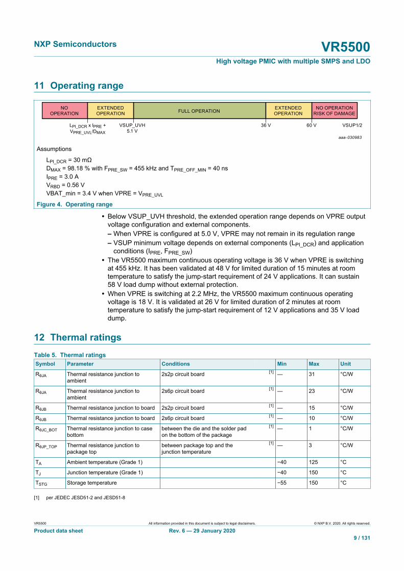
11 Operating range
aaa-030983
NOOPERATION
NO OPERATIONRISK OF DAMAGE
VSUP1/260 V
EXTENDEDOPERATION FULL OPERATION EXTENDED
OPERATION
36 VVSUP_UVH5.1 V
LPI_DCR x IPRE +VPRE_UVL/DMAX
Assumptions
LPI_DCR = 30 mΩDMAX = 98.18 % with FPRE_SW = 455 kHz and TPRE_OFF_MIN = 40 nsIPRE = 3.0 AVRBD = 0.56 VVBAT_min = 3.4 V when VPRE = VPRE_UVL
Figure 4. Operating range
• Below VSUP_UVH threshold, the extended operation range depends on VPRE outputvoltage configuration and external components.– When VPRE is configured at 5.0 V, VPRE may not remain in its regulation range– VSUP minimum voltage depends on external components (LPI_DCR) and application
conditions (IPRE, FPRE_SW)• The VR5500 maximum continuous operating voltage is 36 V when VPRE is switching
at 455 kHz. It has been validated at 48 V for limited duration of 15 minutes at roomtemperature to satisfy the jump-start requirement of 24 V applications. It can sustain58 V load dump without external protection.
• When VPRE is switching at 2.2 MHz, the VR5500 maximum continuous operatingvoltage is 18 V. It is validated at 26 V for limited duration of 2 minutes at roomtemperature to satisfy the jump-start requirement of 12 V applications and 35 V loaddump.
12 Thermal ratingsTable 5. Thermal ratingsSymbol Parameter Conditions Min Max Unit
RθJA Thermal resistance junction toambient
2s2p circuit board [1] — 31 °C/W
RθJA Thermal resistance junction toambient
2s6p circuit board [1] — 23 °C/W
RθJB Thermal resistance junction to board 2s2p circuit board [1] — 15 °C/W
RθJB Thermal resistance junction to board 2s6p circuit board [1] — 10 °C/W
RθJC_BOT Thermal resistance junction to casebottom
between the die and the solder padon the bottom of the package
[1] — 1 °C/W
RθJP_TOP Thermal resistance junction topackage top
between package top and thejunction temperature
[1] — 3 °C/W
TA Ambient temperature (Grade 1) −40 125 °C
TJ Junction temperature (Grade 1) −40 150 °C
TSTG Storage temperature −55 150 °C
[1] per JEDEC JESD51-2 and JESD51-8
NXP Semiconductors VR5500High voltage PMIC with multiple SMPS and LDO
VR5500 All information provided in this document is subject to legal disclaimers. © NXP B.V. 2020. All rights reserved.
Product data sheet Rev. 6 — 29 January 202010 / 131
13 CharacteristicsTable 6. Electrical characteristicsTA = −40 °C to 125 °C, unless otherwise specified. VSUP = VSUP_UVH to 36 V, unless otherwise specified. All voltagesreferenced to ground.
Symbol Parameter Min Typ Max Unit
Power supply
ISUP_NORMAL Current in Normal mode, all regulators ON (IOUT = 0) — 15 25 mA
ISUP_STANDBY Current in Standby mode, all regulators OFF exceptVBOS
— 5 10 mA
ISUP_OFF1 Current in OFF mode (power down), TA < 85 °C — 10 15 μA
ISUP_OFF2 Current in OFF mode (power down), TA = 125 °C — — 25 μA
VSUP_UV7 VSUP undervoltage threshold (7.0 V) 7.2 7.5 7.8 V
VSUP undervoltage threshold high (during power-upand Vsup rising) OTP_VSUP_CFG = 0
4.7 — 5.1 VVSUP_UVH
VSUP undervoltage threshold high (during power-upand Vsup rising) OTP_VSUP_CFG = 1
6.0 — 6.4 V
VSUP undervoltage threshold low (during power-upand Vsup falling) OTP_VSUP_CFG = 0
4.0 — 4.4 VVSUP_UVL
VSUP undervoltage threshold low (during power-upand Vsup falling) OTP_VSUP_CFG = 1
5.3 — 5.7 V
TSUP_UV VSUP_UV7, VSUP_UVH, and VSUP_UVL filtering time 6.0 10 15 μs
14 Functional description
The VR5500 device has two independent logic blocks. The main state machine managesthe power management, the Standby mode and the wake-up sources. The fail-safe statemachine manages the voltage monitoring of the power management.
NXP Semiconductors VR5500High voltage PMIC with multiple SMPS and LDO
VR5500 All information provided in this document is subject to legal disclaimers. © NXP B.V. 2020. All rights reserved.
Product data sheet Rev. 6 — 29 January 202011 / 131
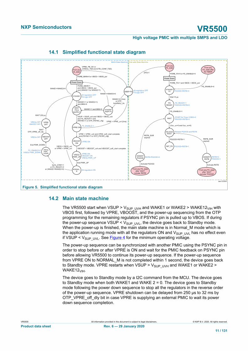
14.1 Simplified functional state diagram
aaa-032948
From anyFS_state
From anyM_state
From anyFS_state after
`8s TIMER'
From any FS_stateafter `WAIT'
exclude `PGOOD'
PORB_FS=0 or FS_ENABLE=0
PORB_FS=1 and VBOS > VBOS_por
PGOOD=RSTB=0
Release PGOOD and RSTB
RSTB=PGOOD=0 RSTB=0,PGOOD=1
FS_READY=1PGOOD=RSTB=0
START 8s Timer if DBG=0PGOOD=RSTB=0
Power Down
STANDBYFS
Wait 10 µs
FS_ENABLE=0
RSTB_DURexpired
RSTB_DURexpired
FSREADY
FS_ENABLE=1
WAIT
(Vxx_uv=0 and Vxx_ov=0)
DEEP-FS
RELEASERESET
PGOOD=RSTB=1
PGOOD=RSTB=1INIT_FS
ASSERTRSTB
Activate RSTB
From any FS_stateafter `WAIT'
include `RSTB'
ASSERTPGOOD
Activate PGOOD
PORB_MAIN=0 or VBOS < VBOS_por
PORB_MAIN=1and VBOS > VBOS_porand (WAKE1=1or WAKE2=1)
All regulators OFFFS logic OFF
VPRE ONVBOOST ONVREGx PWR_UP
All regulators ON
VPRE > VPRE_uvh and VPRE_soft_start completeand (PSYNC=1 or !OTP_PSYNC_cfg)
VPRE ON
FS_ENABLE=1
VPRE < VPRE_uvl (2ms)
Power Down
STANDBY
(WAKE1=1 or WAKE2=1)and DBG=0
WAKE1=WAKE2=0
WAKE1=1 and DBG=0
WAKE1=0 (1ms)or OTP_
AutoRetry_4s
WAKE1=WAKE2=0
VPRE_FB_OV or(VREGx_TSD and OTB_CONF_TSD)
All regulators OFFFS logic OFF
DFS=1
Fail-safe State MachineMAIN State Machine
WAITFS &
SUPPLYSTANDBYDEEP-FS
VSUP > VSUP_uvh and VBOS > VBOS_uvhand FS_READY=1 and(PSYNC=1 or OTP_PSYNC_cfg)
VPRE ON
VBOOSTON
VBOOST > VBOOST_uvh and VBOOST_soft_start complete
VREGxPWR_UP
VPREOFF
VBOOSTOFF
End PWR_DOWN
VREGx OFF
VREGx OFFVBOOST OFF
WAIT 250 µs
FS_ENABLE=0VREGx PWR_DOWN
GoTo_STBY=1or FS_READY=0
or (WAKE1=WAKE2=0)
VBOS < VBOS_uvlor VPRE < VPRE_uvl
WAITOTP_VPRE_off_dly
VREGxPWR_DOWN
End PWR_UP
NORMAL_M
Figure 5. Simplified functional state diagram
14.2 Main state machineThe VR5500 start when VSUP > VSUP_UVH and WAKE1 or WAKE2 > WAKE12VIH withVBOS first, followed by VPRE, VBOOST, and the power-up sequencing from the OTPprogramming for the remaining regulators if PSYNC pin is pulled up to VBOS. If duringthe power-up sequence VSUP < VSUP_UVL, the device goes back to Standby mode.When the power-up is finished, the main state machine is in Normal_M mode which isthe application running mode with all the regulators ON and VSUP_UVL has no effect evenif VSUP < VSUP_UVL. See Figure 4 for the minimum operating voltage.
The power-up sequence can be synchronized with another PMIC using the PSYNC pin inorder to stop before or after VPRE is ON and wait for the PMIC feedback on PSYNC pinbefore allowing VR5500 to continue its power-up sequence. If the power-up sequencefrom VPRE ON to NORMAL_M is not completed within 1 second, the device goes backto Standby mode. VPRE restarts when VSUP > VSUP_UVH and WAKE1 or WAKE2 >WAKE12VIH.
The device goes to Standby mode by a I2C command from the MCU. The device goesto Standby mode when both WAKE1 and WAKE 2 = 0. The device goes to Standbymode following the power down sequence to stop all the regulators in the reverse orderof the power-up sequence. VPRE shutdown can be delayed from 250 μs to 32 ms byOTP_VPRE_off_dly bit in case VPRE is supplying an external PMIC to wait its powerdown sequence completion.

NXP Semiconductors VR5500High voltage PMIC with multiple SMPS and LDO
VR5500 All information provided in this document is subject to legal disclaimers. © NXP B.V. 2020. All rights reserved.
Product data sheet Rev. 6 — 29 January 202012 / 131
In case of loss of VPRE (VPRE < VPRE_UVL) or loss of VBOS (VBOS < VBOS_UVL), thedevice stops and goes directly to Standby mode without power down sequence. VPRErestarts when VSUP > VSUP_UVH and WAKE1 or WAKE2 > WAKE12VIH.
In case of VPRE_FB_OV detection, or TSD detection on a regulator depending onOTP_conf_tsd[5:0] bits configuration, or deep fail-safe request from the fail-safe statemachine when DFS = 1, the device stops and goes directly to DEEP-FS mode withoutpower down sequence.
Exit of DEEP-FS mode is only possible by WAKE1 = 0 or after 4 s if the autoretry featureis activated by OTP_Autorety_en bit. The number of autroretry can be limited to 15 orinfinite depending on OTP_Autoretry_infinite bit. VPRE restarts when VSUP > VSUP_UVHand WAKE1 > WAKE12VIH.
14.3 Fail-safe state machineThe fail-safe state machine starts when VBOS > VBOS_POR. RSTB and PGOOD pins arereleased and the initialization of the device is opened.
When RSTB and PGOOD pins are released, the device is ready for application runningmode with all the selected monitoring activated. From now on, the VR5500 reactsby asserting the pins (PGOOD, RSTB) according to its configuration when a fault isdetected.
14.4 Power sequencingVPRE is the first regulator to start automatically, followed by the BOOST, before theSLOT_0. The other regulators are starting from the OTP power sequencing configuration.Seven slots are available to program the start-up sequence of BUCK1, BUCK 2, BUCK 3,LDO1, and LDO2 regulators. The delay between each slot is configurable to 250 µs or 1ms by OTP using OTP_Tslot bit to accommodate the different ramp up speed of BUCK1,BUCK2, and BUCK3.
The power-up sequence starts at SLOT_0 and ends at SLOT_7 while the power downsequence is executed in reverse order. All the SLOTs are executed even if there is noregulator assigned to a SLOT. The regulators assigned to SLOT_7 are not started duringthe power-up sequence. They can be started (or not) later in Normal_M mode with a I2Ccommand to write in M_REG_CTRL1 register, if enabled by OTP.

NXP Semiconductors VR5500High voltage PMIC with multiple SMPS and LDO
VR5500 All information provided in this document is subject to legal disclaimers. © NXP B.V. 2020. All rights reserved.
Product data sheet Rev. 6 — 29 January 202013 / 131
aaa-030985
FromVBOOST ON
VBOOST > VBOOST_uvhand VBOOST_soft_start complete
SLOT_0
ToNORMAL_M
tslot
SLOT_1
tslot
SLOT_2
tslot
SLOT_3
tslot
SLOT_4
tslot
SLOT_5
tslot
SLOT_6
tslot
Figure 6. Power sequencing (VREGx PWR_UP)
Each regulator is assigned to a SLOT by OTP configuration using OTP_VB1S[2:0] forBUCK1, OTP_VB2S[2:0] for BUCK2, OTP_VB3S[2:0] for BUCK3, OTP_LDO1S[2:0] forLDO1 and OTP_LDO2S[2:0] for LDO2.
The different soft start duration of the BUCKs and the LDOs should be considered in theSLOT assignment to achieve the correct sequence.
NXP Semiconductors VR5500High voltage PMIC with multiple SMPS and LDO
VR5500 All information provided in this document is subject to legal disclaimers. © NXP B.V. 2020. All rights reserved.
Product data sheet Rev. 6 — 29 January 202014 / 131
aaa-030986
VSUP1,2
VSUP > VSUP_uvh
WAKE12VIH
VBOS_uvh
VPRE_uvh andVPRE_soft_start complete
VBOOST_uvh andVBOOST_Soft_start complete
VPRE - VBOOST_diode
tslot
WAKE1or WAKE2
VBOS
VPRE
VBOOST
SLOT_0
SLOT_1
SLOT_2
SLOT_6
PGOOD
RSTB
tslot
Note: See Section 14.1 for PGOOD/RSTB released sequence.
Figure 7. Power-up sequence example
The VR5500_OTP_Mapping file used to generate the OTP configuration of the devicedraws the power-up sequence of an OTP configuration in the OTP_conf_summary sheet.
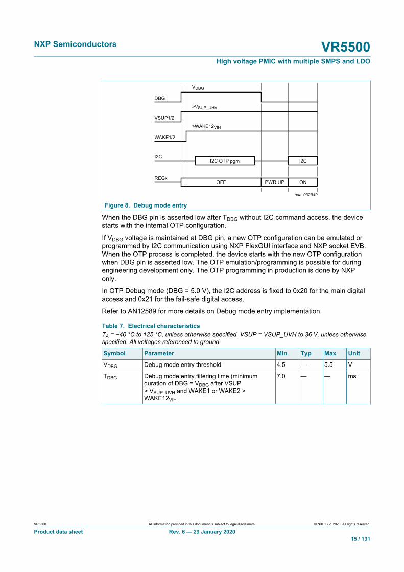
14.5 Debug modeThe VR5500 enters in Debug mode with the sequence described in Figure 8:
1. DBG pin = VDBG and VSUP > VSUP_UVH2. WAKE1 or WAKE2 > WAKE12VIH
VDBG and VSUP can come up at the same time as long as WAKE1 or WAKE2 comes upthe last.
NXP Semiconductors VR5500High voltage PMIC with multiple SMPS and LDO
VR5500 All information provided in this document is subject to legal disclaimers. © NXP B.V. 2020. All rights reserved.
Product data sheet Rev. 6 — 29 January 202015 / 131
aaa-032949
DBG
VDBG
I2C OTP pgm I2C
VSUP1/2
>VSUP_UHV
WAKE1/2
>WAKE12VIH
I2C
OFF ONREGx
PWR UP
Figure 8. Debug mode entry
When the DBG pin is asserted low after TDBG without I2C command access, the devicestarts with the internal OTP configuration.
If VDBG voltage is maintained at DBG pin, a new OTP configuration can be emulated orprogrammed by I2C communication using NXP FlexGUI interface and NXP socket EVB.When the OTP process is completed, the device starts with the new OTP configurationwhen DBG pin is asserted low. The OTP emulation/programming is possible for duringengineering development only. The OTP programming in production is done by NXPonly.
In OTP Debug mode (DBG = 5.0 V), the I2C address is fixed to 0x20 for the main digitalaccess and 0x21 for the fail-safe digital access.
Refer to AN12589 for more details on Debug mode entry implementation.
Table 7. Electrical characteristicsTA = −40 °C to 125 °C, unless otherwise specified. VSUP = VSUP_UVH to 36 V, unless otherwisespecified. All voltages referenced to ground.
Symbol Parameter Min Typ Max Unit
VDBG Debug mode entry threshold 4.5 — 5.5 V
TDBG Debug mode entry filtering time (minimumduration of DBG = VDBG after VSUP> VSUP_UVH and WAKE1 or WAKE2 >WAKE12VIH
7.0 — — ms

NXP Semiconductors VR5500High voltage PMIC with multiple SMPS and LDO
VR5500 All information provided in this document is subject to legal disclaimers. © NXP B.V. 2020. All rights reserved.
Product data sheet Rev. 6 — 29 January 202016 / 131
15 Register mappingAddressRegister M/FS
Adr_5 Adr_4 Adr_3 Adr_2 Adr_1 Adr_0
R/WI2C
Read / Write Reference
M_FLAG 0 0 0 0 0 0 0 1/0 Read / Write Section 16.3
M_MODE 0 0 0 0 0 0 1 1/0 Read / Write Section 16.4
M_REG_CTRL1 0 0 0 0 0 1 0 1/0 Read / Write Section 16.5
M_REG_CTRL2 0 0 0 0 0 1 1 1/0 Read / Write Section 16.6
M_AMUX 0 0 0 0 1 0 0 1/0 Read / Write Section 16.7
M_CLOCK 0 0 0 0 1 0 1 1/0 Read / Write Section 16.8
M_INT_MASK1 0 0 0 0 1 1 0 1/0 Read / Write Section 16.9
M_INT_MASK2 0 0 0 0 1 1 1 1/0 Read / Write Section 16.10
M_FLAG1 0 0 0 1 0 0 0 1/0 Read / Write Section 16.11
M_FLAG2 0 0 0 1 0 0 1 1/0 Read / Write Section 16.12
M_VMON_REGX 0 0 0 1 0 1 0 1/0 Read / Write Section 16.13
M_LVB1_SVS 0 0 0 1 0 1 1 1 Read only Section 16.14
M_MEMORY0 0 1 0 0 0 1 1 1/0 Read / Write Section 16.15
M_MEMORY1 0 1 0 0 1 0 0 1/0 Read / Write Section 16.16
M_DEVICEID 0 1 0 0 1 0 1 1 Read only Section 16.17
FS_GRL_FLAGS 1 0 0 0 0 0 0 1 Read only Section 17.3
FS_I_OVUV_SAFE_REACTION1 1 0 0 0 0 0 1 1/0 Write during INIT thenRead only
Section 17.4
FS_I_NOT_OVUV_SAFE_REACTION1 1 0 0 0 0 1 0 1/0 Write during INIT thenRead only
FS_I_OVUV_SAFE_REACTION2 1 0 0 0 0 1 1 1/0 Write during INIT thenRead only
Section 17.5
FS_I_NOT_OVUV_SAFE_REACTION2 1 0 0 0 1 0 0 1/0 Write during INIT thenRead only
FS_I_FSSM 1 0 0 1 0 0 1 1/0 Write during INIT thenRead only
Section 17.6
FS_I_NOT_FSSM 1 0 0 1 0 1 0 1/0 Write during INIT thenRead only
FS_I_SVS 1 0 0 1 0 1 1 1/0 Write during INIT thenRead only
Section 17.7
FS_I_NOT_SVS 1 0 0 1 1 0 0 1/0 Write during INIT thenRead only
FS_OVUVREG_STATUS 1 0 1 0 0 0 1 1/0 Read / Write Section 17.8
FS_SAFE_IOS 1 0 1 0 0 1 1 1/0 Read / Write Section 17.9
FS_DIAG 1 0 1 0 1 0 0 1/0 Read / Write Section 17.10
FS_INTB_MASK 1 0 1 0 1 0 1 1/0 Read / Write Section 17.11
FS_STATES 1 0 1 0 1 1 0 1/0 Read / Write Section 17.12

NXP Semiconductors VR5500High voltage PMIC with multiple SMPS and LDO
VR5500 All information provided in this document is subject to legal disclaimers. © NXP B.V. 2020. All rights reserved.
Product data sheet Rev. 6 — 29 January 202017 / 131
16 Main register mapping
16.1 Main writing registers overview
Table 8. Main writing registers overviewbit 23 bit 22 bit 21 bit 20 bit 19 bit 18 bit 17 bit 16Logic Register name
bit 15 bit 14 bit 13 bit 12 bit 11 bit 10 bit 9 bit 8
0 0 0 0 0 0 0 0M_FLAG
0 0 0 0 0 0 I2C_M_CRC I2C_M_REQ
0 0 0 0 0 0 0 0M_MODE
0 EXT_FIN_DIS 0 0 0 W2DIS W1DIS GoToSTBY
VPRE_PD_DIS VPDIS BOOSTDIS BUCK1DIS BUCK2DIS BUCK3DIS LDO1DIS LDO2DISM_REG_CTRL1
0 VPEN BOOSTEN BUCK1EN BUCK2EN BUCK3EN LDO1EN LDO2EN
VBSTSR[1:0] BOOSTTSDCFG
BUCK1TSDCFG BUCK2TSDCFG BUCK3TSDCFG LDO1TSDCFG LDO2TSDCFGM_REG_CTRL2
0 0 0 VPRESRLS[1:0] 0 VPRESRHS[1:0]
0 0 0 0 0 0 0 0M_AMUX
0 0 RATIO AMUX[4:0]
MOD_CONF FOUT_MUX_SEL[3:0] FOUT_PHASE[2:0]M_CLOCK
FOUT_CLK_SEL
EXT_FIN_SEL FIN_DIV MOD_EN CLK_TUNE[3 :0]
0 VPREOC_M 0 BUCK1OC_M BUCK2OC_M BUCK3OC_M LDO1OC_M LDO2OC_MM_INT_MASK1
0 0 BOOSTTSD_M BUCK1TSD_M BUCK2TSD_M BUCK3TSD_M LDO1TSD_M LDO2TSD_M
0 0 0 0 VBOOSTOV_M VBOSUVH_M COM_M VPRE_FB_OV_M
M_INT_MASK2
VBOOST_UVH_M
VSUPUV7 0 VPREUVH VSUPUVL_M VSUPUVH_M WAKE1_M WAKE2_M
VBOSUVH VBOOSTUVH VPREOC BUCK1OC BUCK2OC BUCK3OC LDO1OC LDO2OCM_FLAG1
0 VBOOSTOV VBOOSTOT BUCK1OT BUCK2OT BUCK3OT LDO1OT LDO2OT
VPRE_FB_OV VSUPUV7 0 0 0 0 0 0M_FLAG2
VPREUVL VPREUVH VSUPUVL VSUPUVH 0 0 WK2FLG WK1FLG
0 0 0 0 0 0 0 0M_VMON_REGX
0 0 0 0 0 VMON1_REG[2:0]
M_MEMORY0 MEMORY0[15:0]
Main
M_MEMORY1 MEMORY1[15:0]

NXP Semiconductors VR5500High voltage PMIC with multiple SMPS and LDO
VR5500 All information provided in this document is subject to legal disclaimers. © NXP B.V. 2020. All rights reserved.
Product data sheet Rev. 6 — 29 January 202018 / 131
16.2 Main reading registers overview
Table 9. Main reading registers overviewbit 23 bit 22 bit 21 bit 20 bit 19 bit 18 bit 17 bit 16Logic Register name
bit 15 bit 14 bit 13 bit 12 bit 11 bit 10 bit 9 bit 8
COM_ERR WU_G VPRE_G VBOOST_G VBUCK1_G VBUCK2_G VBUCK3_G VLDO1_GM_FLAG
VLDO2_G 0 0 0 0 0 I2C_M_CRC I2C_M_REQ
RESERVED RESERVED RESERVED RESERVED RESERVED RESERVED RESERVED PLL_LOCK_RTM_MODE
EXT_FIN_SEL_RT
RESERVED MAIN_NORMAL RESERVED RESERVED W2DIS W1DIS RESERVED
VPRE_PD_DIS VPDIS BOOSTDIS BUCK1DIS BUCK2DIS BUCK3DIS LDO1DIS LDO2DISM_REG_CTRL1
0 VPEN BOOSTEN BUCK1EN BUCK2EN BUCK3EN LDO1EN LDO2EN
VBSTSR[1:0] BOOSTTSDCFG
BUCK1TSDCFG BUCK2TSDCFG BUCK3TSDCFG LDO1TSDCFG LDO2TSDCFGM_REG_CTRL2
RESERVED RESERVED RESERVED VPRESRLS[1:0] RESERVED VPRESRHS[1:0]
RESERVED RESERVED RESERVED RESERVED RESERVED RESERVED RESERVED RESERVEDM_AMUX
RESERVED RESERVED RATIO AMUX[4:0]
MOD_CONF FOUT_MUX_SEL[3:0] FOUT_PHASE[2:0]M_CLOCK
FOUT_CLK_SEL
RESERVED FIN_DIV MOD_EN CLK_TUNE[3 :0]
RESERVED VPREOC_M RESERVED BUCK1OC_M BUCK2OC_M BUCK3OC_M LDO1OC_M LDO2OC_MM_INT_MASK1
RESERVED RESERVED BOOSTTSD_M BUCK1TSD_M BUCK2TSD_M BUCK3TSD_M LDO1TSD_M LDO2TSD_M
RESERVED RESERVED RESERVED RESERVED VBOOSTOV_M VBOSUVH_M COM_M VPRE_FB_OV_M
M_INT_MASK2
VBOOST_UVH_M
VSUPUV7_M RESERVED VPREUVH_M VSUPUV_M VSUPUVH_M WAKE1_M WAKE2_M
VBOSUVH VBOOSTUVH VPREOC BUCK1OC BUCK2OC BUCK3OC LDO1OC LDO2OCM_FLAG1
CLK_FIN_DIV_OK
VBOOSTOV VBOOSTOT BUCK1OT BUCK2OT BUCK3OT LDO1OT LDO2OT
VPRE_FB_OV VSUPUV7 BOOST_ST BUCK1_ST BUCK2_ST BUCK3_ST LDO1_ST LDO2_STM_FLAG2
VPREUVL VPREUVH VSUPUVL VSUPUVH WK2RT WK1RT WK2FLG WK1FLG
RESERVED RESERVED RESERVED RESERVED RESERVED RESERVED RESERVED RESERVEDM_VMON_REGX
RESERVED RESERVED RESERVED RESERVED RESERVED VMON1_REG[2:0]
RESERVED RESERVED RESERVED RESERVED RESERVED RESERVED RESERVED RESERVEDM_LVB1_SVS
RESERVED RESERVED RESERVED LVB1_SVS[4:0]
M_MEMORY0 MEMORY0[15:0]
M_MEMORY1 MEMORY1[15:0]
FM_REV[3:0] MM_REV[3:0]
Main
M_DEVICEID
DEVICEID[7:0]
16.3 M_FLAG register
Table 10. M_FLAG register bit allocationBit 23 22 21 20 19 18 17 16
Write 0 0 0 0 0 0 0 0
Read COM_ERR WU_G VPRE_G VBOOST_G VBUCK1_G VBUCK2_G VBUCK3_G VLDO1_G
Reset 0 1 1 0 0 0 0 0
Bit 15 14 13 12 11 10 9 8
Write 0 0 0 0 0 0 I2C_M_CRC I2C_M_REQ
Read VLDO2_G 0 0 0 0 0 I2C_M_CRC I2C_M_REQ
Reset 0 0 0 0 0 0 0 0

NXP Semiconductors VR5500High voltage PMIC with multiple SMPS and LDO
VR5500 All information provided in this document is subject to legal disclaimers. © NXP B.V. 2020. All rights reserved.
Product data sheet Rev. 6 — 29 January 202019 / 131
Table 11. M_FLAG register bit descriptionBit Symbol Description
Report an error in the communication (I2C)COM_ERR = I2C_M_CRC or I2C_M_REQ or FS_COM_G
0 No failure
1 Failure
23 COM_ERR
Reset condition: Real-time information - cleared when all individual bits are cleared
Report a wake-up event by WAKE1 or WAKE2WU_G = WK1FLG or WK2FLG
0 No wake event
1 Wake event
22 WU_G
Reset condition: Real-time information - cleared when all individual bits are cleared
Report an event on VPRE (status change or failure)VPRE_G = VPREOC or VPREUVH or VPREUVL or VPRE_FB_OV
0 No event
1 Event occurred
21 VPRE_G
Reset condition: Real-time information - cleared when all individual bits are cleared
Report an event on VBOOST (status change or failure)VBOOST_G = VBOOSTOT or BOOSTOV
0 No event
1 Event occurred
20 VBOOST_G
Reset condition: Real-time information - cleared when all individual bits are cleared
Report an event on BUCK1 (status change or failure)VBUCK1_G = BUCK1OC or BUCK1OT
0 No event
1 Event occurred
19 VBUCK1_G
Reset condition: Real-time information - cleared when all individual bits are cleared
Report an event on BUCK2 (status change or failure)VBUCK2_G = BUCK2OC or BUCK2OT
0 No event
1 Event occurred
18 VBUCK2_G
Reset condition: Real-time information - cleared when all individual bits are cleared
Report an event on BUCK3 (status change or failure)VBUCK3_G = BUCK3OC or BUCK3OT
0 No event
1 Event occurred
17 VBUCK3_G
Reset condition: Real-time information - cleared when all individual bits are cleared
Report an event on LDO1 (status change or failure)VLDO1_G = LDO1OC or LDO1OT
0 No event
1 Event occurred
16 VLDO1_G
Reset condition: Real-time information
NXP Semiconductors VR5500High voltage PMIC with multiple SMPS and LDO
VR5500 All information provided in this document is subject to legal disclaimers. © NXP B.V. 2020. All rights reserved.
Product data sheet Rev. 6 — 29 January 202020 / 131
Bit Symbol Description
Report an event on LDO2 (status change or failure)VLDO2_G = LDO2OC or LDO2OT
0 No event
1 Event occurred
15 VLDO2_G
Reset condition: Real-time information
Main domain I2C communication CRC issue
0 No error
1 Error detected in the I2C CRC
9 I2C_M_CRC
Reset condition: POR / clear on write (write ‘1’)
Invalid main domain I2C access (wrong Write or Read, Write to INIT registers in normal mode,wrong address)
0 No error
1 I2C violation
8 I2C_M_REQ
Reset condition: POR / clear on Write (write ‘1’)
16.4 M_MODE register
Table 12. M_MODE register bit allocationBit 23 22 21 20 19 18 17 16
Write 0 0 0 0 0 0 0 0
Read RESERVED RESERVED RESERVED RESERVED RESERVED RESERVED RESERVED PLL_LOCK_RT
Reset 0 0 0 0 0 0 0 0
Bit 15 14 13 12 11 10 9 8
Write 0 EXT_FIN_DIS
0 0 0 W2DIS W1DIS GoToSTBY
Read EXT_FIN_SEL_RT
RESERVED MAIN_NORMAL
RESERVED RESERVED W2DIS W1DIS RESERVED
Reset 0 0 1 0 0 0 0 0
Table 13. M_MODE register bit descriptionBit Symbol Description
Real-time status of the PPL
0 PLL not locked
1 PLL locked
16 PLL_LOCK_RT
Reset condition: POR
Real-time status of FIN clock selection
0 Internal clock oscillator is selected
1 External FIN clock is selected
15 EXT_FIN_SEL_RT
Reset condition: POR

NXP Semiconductors VR5500High voltage PMIC with multiple SMPS and LDO
VR5500 All information provided in this document is subject to legal disclaimers. © NXP B.V. 2020. All rights reserved.
Product data sheet Rev. 6 — 29 January 202021 / 131
Bit Symbol Description
Disable request of EXT FIN selection at PLL input
0 No effect
1 Disable FIN selection
14 EXT_FIN_DIS
Reset condition: POR
Main state machine status
0 Main state machine is not in Normal mode
1 Main state machine is in Normal mode
13 MAIN_NORMAL
Reset condition: POR
WAKE2 wake up disable
0 wake up enable
1 wake up disable
10 W2DIS
Reset condition: POR
WAKE1 wake up disable
0 Wake up enable
1 Wake up disable
9 W1DIS
Reset condition: POR
Standby mode request
0 Device remains in current state
1 Device enters in Standby mode
8 GOTOSTBY
Reset condition: POR
16.5 M_REG_CTRL1 register
Table 14. M_REG_CTRL1 register bit allocationBit 23 22 21 20 19 18 17 16
Write VPRE_PD_DIS
VPDIS BOOSTDIS BUCK1DIS BUCK2DIS BUCK3DIS LDO1DIS LDO2DIS
Read VPRE_PD_DIS
RESERVED RESERVED RESERVED RESERVED RESERVED RESERVED RESERVED
Reset 0 0 0 0 0 0 0 0
Bit 15 14 13 12 11 10 9 8
Write 0 VPEN BOOSTEN BUCK1EN BUCK2EN BUCK3EN LDO1EN LDO2EN
Read RESERVED RESERVED RESERVED RESERVED RESERVED RESERVED RESERVED RESERVED
Reset 0 0 0 0 0 0 0 0
Table 15. M_REG_CTRL1 register bit descriptionBit Symbol Description
Force disable of VPRE pull-down
0 No effect (VPRE pull-down is automatically controlled by the logic)
1 VPRE pull-down disable request
23 VPRE_PD_DIS
Reset condition: POR

NXP Semiconductors VR5500High voltage PMIC with multiple SMPS and LDO
VR5500 All information provided in this document is subject to legal disclaimers. © NXP B.V. 2020. All rights reserved.
Product data sheet Rev. 6 — 29 January 202022 / 131
Bit Symbol Description
Disable request of VPRE
0 No effect (regulator remains in existing state)
1 VPRE disable request
22 VPDIS
Reset condition: POR
Disable request of BOOST
0 No effect (regulator remains in existing state)
1 BOOST disable request
21 BOOSTDIS
Reset condition: POR
Disable request of BUCK1
0 No effect (regulator remains in existing state)
1 BUCK1 disable request
20 BUCK1DIS
Reset condition: POR
Disable request of BUCK2
0 No effect (regulator remains in existing state)
1 BUCK2 disable request
19 BUCK2DIS
Reset condition: POR
Disable request of BUCK3
0 No effect (regulator remains in existing state)
1 BUCK3 disable request
18 BUCK3DIS
Reset condition: POR
Disable request of LDO1
0 No effect (regulator remains in existing state)
1 LDO1 disable request
17 LDO1DIS
Reset condition: POR
Disable request of LDO2
0 no effect (regulator remains in existing state)
1 LDO2 disable request
16 LDO2DIS
Reset condition: POR
Enable request of VPRE
0 No effect (regulator remains in existing state)
1 VPRE enable request (after a VPDIS request)
14 VPEN
Reset condition: POR
Enable request of BOOST
0 No effect (regulator remains in existing state)
1 BOOST enable request
13 BOOSTEN
Reset condition: POR
Enable request of BUCK1
0 No effect (regulator remains in existing state)
1 BUCK1 enable request
12 BUCK1EN
Reset condition: POR
NXP Semiconductors VR5500High voltage PMIC with multiple SMPS and LDO
VR5500 All information provided in this document is subject to legal disclaimers. © NXP B.V. 2020. All rights reserved.
Product data sheet Rev. 6 — 29 January 202023 / 131
Bit Symbol Description
Enable request of BUCK2
0 No effect (regulator remains in existing state)
1 BUCK2 enable request
11 BUCK2EN
Reset condition: POR
Enable request of BUCK3
0 No effect (regulator remains in existing state)
1 BUCK3 enable request
10 BUCK3EN
Reset condition: POR
Enable request of LDO1
0 No effect (regulator remains in existing state)
1 LDO1 enable request
9 LDO1EN
Reset condition: POR
Enable request of LDO2
0 no effect (regulator remains in existing state)
1 LDO2 enable request
8 LDO2EN
Reset condition: POR
16.6 M_REG_CTRL2 register
Table 16. M_REG_CTRL2 register bit allocationBit 23 22 21 20 19 18 17 16
Write VBSTSR[1:0] BOOSTTSDCFG
BUCK1TSDCFG
BUCK2TSDCFG
BUCK3TSDCFG
LDO1TSDCFG
LDO2TSDCFG
Read VBSTSR[1:0] BOOSTTSDCFG
BUCK1TSDCFG
BUCK2TSDCFG
BUCK3TSDCFG
LDO1TSDCFG
LDO2TSDCFG
Reset OTP OTP OTP OTP OTP OTP OTP OTP
Bit 15 14 13 12 11 10 9 8
Write 0 0 0 VPRESRLS[1:0] 0 VPRESRHS[1:0]
Read RESERVED RESERVED RESERVED VPRESRLS[1:0] RESERVED VPRESRHS[1:0]
Reset 0 0 0 1 1 0 OTP OTP
Table 17. M_REG_CTRL2 register bit descriptionBit Symbol Description
VBOOST low-side slew rate control
00 50 V/μs - slow
01 100 V/μs – medium
10 300 V/μs – fast
11 500 V/μs – ultra fast
23 to 22 VBSTSR[1:0]
Reset condition: POR
NXP Semiconductors VR5500High voltage PMIC with multiple SMPS and LDO
VR5500 All information provided in this document is subject to legal disclaimers. © NXP B.V. 2020. All rights reserved.
Product data sheet Rev. 6 — 29 January 202024 / 131
Bit Symbol Description
BOOST behavior in case of TSD
0 Regulator shutdown
1 Regulator shutdown and state machine transition to DEEP-FS
21 BOOSTTSDCFG
Reset condition: POR
BUCK1 behavior in case of TSD
0 Regulator shutdown
1 Regulator shutdown and state machine transition to DEEP-FS
20 BUCK1TSDCFG
Reset condition: POR
BUCK2 behavior in case of TSD
0 Regulator shutdown
1 Regulator shutdown and state machine transition to DEEP-FS
19 BUCK2TSDCFG
Reset condition: POR
BUCK3 behavior in case of TSD
0 Regulator shutdown
1 Regulator shutdown and state machine transition to DEEP-FS
18 BUCK3TSDCFG
Reset condition: POR
LDO1 behavior in case of TSD
0 Regulator shutdown
1 Regulator shutdown and state machine transition to DEEP-FS
17 LDO1TSDCFG
Reset condition: POR
LDO2 behavior in case of TSD
0 Regulator shutdown
1 Regulator shutdown and state machine transition to DEEP-FS
16 LDO2TSDCFG
Reset condition: POR
VPRE low-side slew rate control
00 130 mA typical drive capability - slow
01 260 mA typical drive capability - medium
10 520 mA typical drive capability - fast
11 900 mA typical drive capability - ultra fast
12 to 11 VPRESRLS[1:0]
Reset condition: POR
VPRE high-side slew rate control
00 130 mA typical drive capability - slow
01 260 mA typical drive capability - medium
10 520 mA typical drive capability - fast
11 900 mA typical drive capability - ultra fast
9 to 8 VPRESRHS[1:0]
Reset condition: POR
NXP Semiconductors VR5500High voltage PMIC with multiple SMPS and LDO
VR5500 All information provided in this document is subject to legal disclaimers. © NXP B.V. 2020. All rights reserved.
Product data sheet Rev. 6 — 29 January 202025 / 131
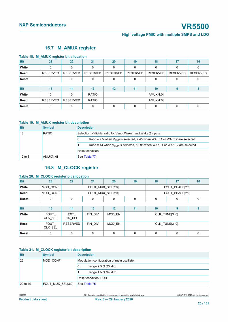
16.7 M_AMUX register
Table 18. M_AMUX register bit allocationBit 23 22 21 20 19 18 17 16
Write 0 0 0 0 0 0 0 0
Read RESERVED RESERVED RESERVED RESERVED RESERVED RESERVED RESERVED RESERVED
Reset 0 0 0 0 0 0 0 0
Bit 15 14 13 12 11 10 9 8
Write 0 0 RATIO AMUX[4:0]
Read RESERVED RESERVED RATIO AMUX[4:0]
Reset 0 0 0 0 0 0 0 0
Table 19. M_AMUX register bit descriptionBit Symbol Description
Selection of divider ratio for Vsup, Wake1 and Wake 2 inputs
0 Ratio = 7.5 when VSUP is selected, 7.45 when WAKE1 or WAKE2 are selected
1 Ratio = 14 when VSUP is selected, 13.85 when WAKE1 or WAKE2 are selected
13 RATIO
Reset condition
12 to 8 AMUX[4:0] See Table 77
16.8 M_CLOCK register
Table 20. M_CLOCK register bit allocationBit 23 22 21 20 19 18 17 16
Write MOD_CONF FOUT_MUX_SEL[3:0] FOUT_PHASE[2:0]
Read MOD_CONF FOUT_MUX_SEL[3:0] FOUT_PHASE[2:0]
Reset 0 0 0 0 0 0 0 0
Bit 15 14 13 12 11 10 9 8
Write FOUT_CLK_SEL
EXT_FIN_SEL
FIN_DIV MOD_EN CLK_TUNE[3 :0]
Read FOUT_CLK_SEL
RESERVED FIN_DIV MOD_EN CLK_TUNE[3 :0]
Reset 0 0 0 0 0 0 0 0
Table 21. M_CLOCK register bit descriptionBit Symbol Description
Modulation configuration of main oscillator
0 range ± 5 % 23 kHz
1 range ± 5 % 94 kHz
23 MOD_CONF
Reset condition: POR
22 to 19 FOUT_MUX_SEL[3:0] See Table 75

NXP Semiconductors VR5500High voltage PMIC with multiple SMPS and LDO
VR5500 All information provided in this document is subject to legal disclaimers. © NXP B.V. 2020. All rights reserved.
Product data sheet Rev. 6 — 29 January 202026 / 131
Bit Symbol Description
FOUT phase shifting configuration (see Section 25.2 "Phase shifting")
000 No shift
001 Shifted by 1 clock cycle of CLK running at 20 MHz
010 Shifted by 2 clock cycle of CLK running at 20 MHz
011 Shifted by 3 clock cycle of CLK running at 20 MHz
100 Shifted by 4 clock cycle of CLK running at 20 MHz
101 Shifted by 5 clock cycle of CLK running at 20 MHz
110 Shifted by 6 clock cycle of CLK running at 20 MHz
111 Shifted by 7 clock cycle of CLK running at 20 MHz
18 to 16 FOUT_PHASE[2:0]
Reset condition: POR
FOUT_clk frequency selection (CLK1 or CLK2)
0 FOUT_clk = CLK1
1 FOUT_clk = CLK2
15 FOUT_CLK_SEL
Reset condition: POR
Enable request of EXT FIN selection at PLL input
0 No effect
1 FIN selection request
14 EXT_FIN_SEL
Reset condition: POR
FIN input signal divider selection
0 Divider by 1
1 Divider by 6
13 FIN_DIV
Reset condition: POR
Modulation activation of main oscillator
0 Modulation disabled
1 Modulation enabled
12 MOD_EN
Reset condition: POR
11 to 8 CLK_TUNE[3:0] See Table 74
16.9 M_INT_MASK1 register
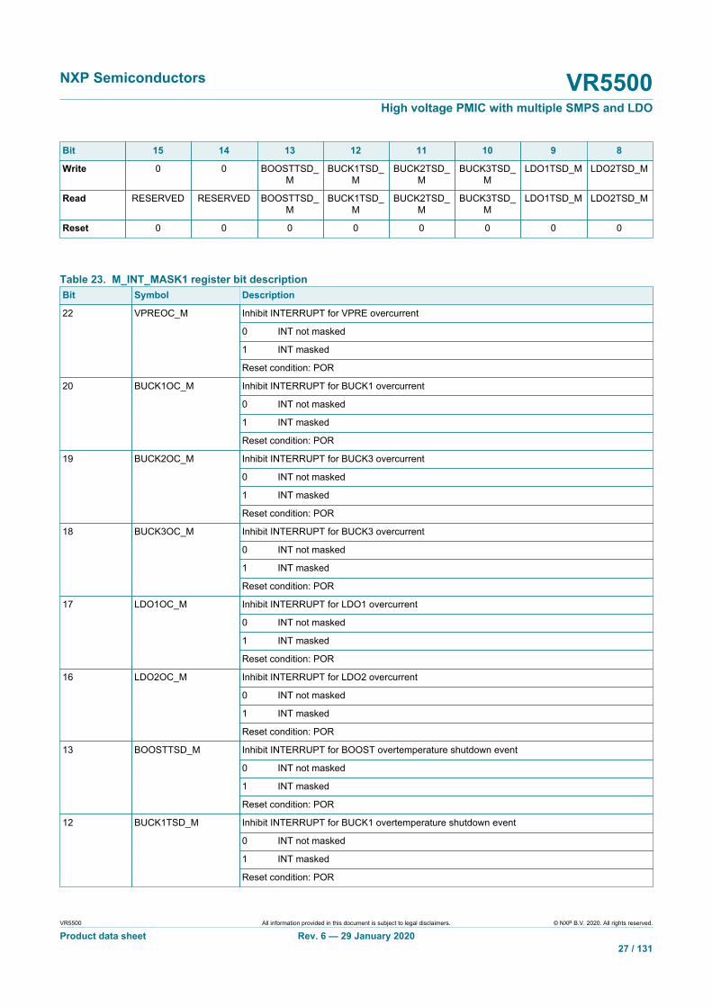
Table 22. M_INT_MASK1 register bit allocationBit 23 22 21 20 19 18 17 16
Write 0 VPREOC_M 0 BUCK1OC_M
BUCK2OC_M
BUCK3OC_M
LDO1OC_M LDO2OC_M
Read RESERVED VPREOC_M RESERVED BUCK1OC_M
BUCK2OC_M
BUCK3OC_M
LDO1OC_M LDO2OC_M
Reset 0 0 0 0 0 0 0 0
NXP Semiconductors VR5500High voltage PMIC with multiple SMPS and LDO
VR5500 All information provided in this document is subject to legal disclaimers. © NXP B.V. 2020. All rights reserved.
Product data sheet Rev. 6 — 29 January 202027 / 131
Bit 15 14 13 12 11 10 9 8
Write 0 0 BOOSTTSD_M
BUCK1TSD_M
BUCK2TSD_M
BUCK3TSD_M
LDO1TSD_M LDO2TSD_M
Read RESERVED RESERVED BOOSTTSD_M
BUCK1TSD_M
BUCK2TSD_M
BUCK3TSD_M
LDO1TSD_M LDO2TSD_M
Reset 0 0 0 0 0 0 0 0
Table 23. M_INT_MASK1 register bit descriptionBit Symbol Description
Inhibit INTERRUPT for VPRE overcurrent
0 INT not masked
1 INT masked
22 VPREOC_M
Reset condition: POR
Inhibit INTERRUPT for BUCK1 overcurrent
0 INT not masked
1 INT masked
20 BUCK1OC_M
Reset condition: POR
Inhibit INTERRUPT for BUCK3 overcurrent
0 INT not masked
1 INT masked
19 BUCK2OC_M
Reset condition: POR
Inhibit INTERRUPT for BUCK3 overcurrent
0 INT not masked
1 INT masked
18 BUCK3OC_M
Reset condition: POR
Inhibit INTERRUPT for LDO1 overcurrent
0 INT not masked
1 INT masked
17 LDO1OC_M
Reset condition: POR
Inhibit INTERRUPT for LDO2 overcurrent
0 INT not masked
1 INT masked
16 LDO2OC_M
Reset condition: POR
Inhibit INTERRUPT for BOOST overtemperature shutdown event
0 INT not masked
1 INT masked
13 BOOSTTSD_M
Reset condition: POR
Inhibit INTERRUPT for BUCK1 overtemperature shutdown event
0 INT not masked
1 INT masked
12 BUCK1TSD_M
Reset condition: POR

NXP Semiconductors VR5500High voltage PMIC with multiple SMPS and LDO
VR5500 All information provided in this document is subject to legal disclaimers. © NXP B.V. 2020. All rights reserved.
Product data sheet Rev. 6 — 29 January 202028 / 131
Bit Symbol Description
Inhibit INTERRUPT for BUCK2 overtemperature shutdown event
0 INT not masked
1 INT masked
11 BUCK2TSD_M
Reset condition: POR
Inhibit INTERRUPT for BUCK3 overtemperature shutdown event
0 INT not masked
1 INT masked
10 BUCK3TSD_M
Reset condition: POR
Inhibit INTERRUPT for LDO1 overtemperature shutdown event
0 INT not masked
1 INT masked
9 LDO1TSD_M
Reset condition: POR
Inhibit INTERRUPT for LDO2 overtemperature shutdown event
0 INT not masked
1 INT masked
8 LDO2TSD_M
Reset condition: POR
16.10 M_INT_MASK2 register
Table 24. M_INT_MASK2 register bit allocationBit 23 22 21 20 19 18 17 16
Write 0 0 0 0 VBOOSTOV_M
VBOSUVH_M
COM_M VPRE_FB_OV_M
Read RESERVED RESERVED RESERVED RESERVED VBOOSTOV_M
VBOSUVH_M
COM_M VPRE_FB_OV_M
Reset 0 0 0 0 0 0 0 0
Bit 15 14 13 12 11 10 9 8
Write VBOOST_UVH_M
VSUPUV7_M 0 VPREUVH_M
VSUPUVL_M VSUPUVH_M
WAKE1_M WAKE2_M
Read VBOOST_UVH_M
VSUPUV7_M RESERVED VPREUVH_M
VSUPUVL_M VSUPUVH_M
WAKE1_M WAKE2_M
Reset 0 0 0 0 0 0 0 0
Table 25. M_INT_MASK2 register bit descriptionBit Symbol Description
Inhibit INTERRUPT for VBOOST_OV any transition
0 INT not masked
1 INT masked
19 VBOOSTOV_M
Reset condition: POR
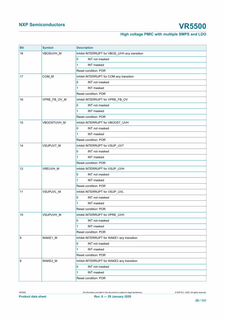
NXP Semiconductors VR5500High voltage PMIC with multiple SMPS and LDO
VR5500 All information provided in this document is subject to legal disclaimers. © NXP B.V. 2020. All rights reserved.
Product data sheet Rev. 6 — 29 January 202029 / 131
Bit Symbol Description
Inhibit INTERRUPT for VBOS_UVH any transition
0 INT not masked
1 INT masked
18 VBOSUVH_M
Reset condition: POR
Inhibit INTERRUPT for COM any transition
0 INT not masked
1 INT masked
17 COM_M
Reset condition: POR
Inhibit INTERRUPT for VPRE_FB_OV
0 INT not masked
1 INT masked
16 VPRE_FB_OV_M
Reset condition: POR
Inhibit INTERRUPT for VBOOST_UVH
0 INT not masked
1 INT masked
15 VBOOSTUVH_M
Reset condition: POR
Inhibit INTERRUPT for VSUP_UV7
0 INT not masked
1 INT masked
14 VSUPUV7_M
Reset condition: POR
Inhibit INTERRUPT for VSUP_UVH
0 INT not masked
1 INT masked
12 VREUVH_M
Reset condition: POR
Inhibit INTERRUPT for VSUP_UVL
0 INT not masked
1 INT masked
11 VSUPUVL_M
Reset condition: POR
Inhibit INTERRUPT for VPRE_UVH
0 INT not masked
1 INT masked
10 VSUPUVH_M
Reset condition: POR
Inhibit INTERRUPT for WAKE1 any transition
0 INT not masked
1 INT masked
9 WAKE1_M
Reset condition: POR
Inhibit INTERRUPT for WAKE2 any transition
0 INT not masked
1 INT masked
8 WAKE2_M
Reset condition: POR

NXP Semiconductors VR5500High voltage PMIC with multiple SMPS and LDO
VR5500 All information provided in this document is subject to legal disclaimers. © NXP B.V. 2020. All rights reserved.
Product data sheet Rev. 6 — 29 January 202030 / 131
16.11 M_FLAG1 registerWhen device starts-up, it is recommended to clear all the flags by writing 1 on all bits.
Table 26. M_FLAG1 register bit allocationBit 23 22 21 20 19 18 17 16
Write VBOSUVH VBOOSTUVH
VPREOC BUCK1OC BUCK2OC BUCK3OC LDO1OC LDO2OC
Read VBOSUVH VBOOSTUVH
VPREOC BUCK1OC BUCK2OC BUCK3OC LDO1OC LDO2OC
Reset 1 1 0 0 0 0 0 0
Bit 15 14 13 12 11 10 9 8
Write 0 VBOOSTOV VBOOSTOT BUCK1OT BUCK2OT BUCK3OT LDO1OT LDO2OT
Read CLK_FIN_DIV_OK
VBOOSTOV VBOOSTOT BUCK1OT BUCK2OT BUCK3OT LDO1OT LDO2OT
Reset 0 0 0 0 0 0 0 0
Table 27. M_FLAG1 register bit descriptionBit Symbol Description
VBOS undervoltage high event (falling)
0 No event
1 Event occurred
23 VBOSUVH
Reset condition: POR / Clear on Write (write ‘1’)
VBOOST undervoltage high event (falling)
0 No event
1 Event occurred
22 VBOOSTUVH
Reset condition: POR / Clear on Write (write ‘1’)
VPRE overcurrent event
0 No event
1 Event occurred
21 VPREOC
Reset condition: POR / Clear on Write (write ‘1’)
BUCK1 overcurrent event
0 No event
1 Event occurred
20 BUCK1OC
Reset condition: POR / Clear on Write (write ‘1’)
BUCK3 overcurrent event
0 No event
1 Event occurred
19 BUCK2OC
Reset condition: POR / Clear on Write (write ‘1’)
BUCK3 overcurrent
0 No event
1 Event occurred
18 BUCK3OC
Reset condition: POR / Clear on Write (write ‘1’)

NXP Semiconductors VR5500High voltage PMIC with multiple SMPS and LDO
VR5500 All information provided in this document is subject to legal disclaimers. © NXP B.V. 2020. All rights reserved.
Product data sheet Rev. 6 — 29 January 202031 / 131
Bit Symbol Description
LDO2 overcurrent
0 No event
1 Event occurred
17 LDO1OC
Reset condition: POR / Clear on Write (write ‘1’)
LDO1 overcurrent
0 No event
1 Event occurred
16 LDO2OC
Reset condition: POR / Clear on Write (write ‘1’)
CLK_FIN_DIV monitoring
0 Not OK: FINERR_LONG < CLK_FIN_DIV deviation < FINERR_SHORT
1 OK: FINERR_SHORT < CLK_FIN_DIV deviation < FINERR_LONG
15 CLK_FIN_DIV_OK
Reset condition: Real time information
VBOOST overvoltage protection event
0 No event
1 Event occurred
14 VBOOSTOV
Reset condition: POR / Clear on Write (write ‘1’)
VBOOST overtemperature shutdown event
0 No event
1 Event occurred
13 VBOOSTOT
Reset condition: POR / Clear on Write (write ‘1’)
BUCK1 overtemperature shutdown event
0 No event
1 Event occurred
12 BUCK1OT
Reset condition: POR / Clear on Write (write ‘1’)
BUCK2 overtemperature shutdown event
0 No event
1 Event occurred
11 BUCK2OT
Reset condition: POR / Clear on Write (write ‘1’)
BUCK3 overtemperature shutdown event
0 No event
1 Event occurred
10 BUCK3OT
Reset condition: POR / Clear on Write (write ‘1’)
LDO1 overtemperature shutdown event
0 No event
1 Event occurred
9 LDO1OT
Reset condition: POR / Clear on Write (write ‘1’)
LDO2 overtemperature shutdown event
0 No event
1 Event occurred
8 LDO2OT
Reset condition: POR / Clear on Write (write ‘1’)

NXP Semiconductors VR5500High voltage PMIC with multiple SMPS and LDO
VR5500 All information provided in this document is subject to legal disclaimers. © NXP B.V. 2020. All rights reserved.
Product data sheet Rev. 6 — 29 January 202032 / 131
16.12 M_FLAG2 registerWhen device starts-up, it is recommended to clear all the flags by writing 1 on all bits.
Table 28. M_FLAG2 register bit allocationBit 23 22 21 20 19 18 17 16
Write VPRE_FB_OV
VSUPUV7 0 0 0 0 0 0
Read VPRE_FB_OV
VSUPUV7 BOOST_ST BUCK1_ST BUCK2_ST BUCK3_ST LDO1_ST LDO2_ST
Reset 0 1 1 1 1 1 1 1
Bit 15 14 13 12 11 10 9 8
Write VPREUVL VPREUVH VSUPUVL VSUPUVH 0 0 WK2FLG WK1FLG
Read VPREUVL VPREUVH VSUPUVL VSUPUVH WK2RT WK1RT WK2FLG WK1FLG
Reset 1 1 1 1 0 1 0 1
Note: Reset value for VR5500, wake up by Wake1, all regulators started by defaultduring power-up sequence.
Table 29. M_FLAG2 register bit descriptionBit Symbol Description
VPRE_FB_OV event
0 No event
1 Event occurred
23 VPRE_FB_OV
Reset condition: POR / Clear on Write (write ‘1’)
VSUP_UV7 event
0 No event
1 Event occurred
22 VSUPUV7
Reset condition: POR / Clear on Write (write ‘1’)
BOOST state
0 Regulator OFF
1 Regulator ON
21 BOOST_ST
Reset condition: Real-time information
BUCK1 state
0 Regulator OFF
1 Regulator ON
20 BUCK1_ST
Reset condition: Real-time information
BUCK2 state
0 Regulator OFF
1 Regulator ON
19 BUCK2_ST
Reset condition: Real-time information
BUCK3 state
0 Regulator OFF
1 Regulator ON
18 BUCK3_ST
Reset condition: Real-time information

NXP Semiconductors VR5500High voltage PMIC with multiple SMPS and LDO
VR5500 All information provided in this document is subject to legal disclaimers. © NXP B.V. 2020. All rights reserved.
Product data sheet Rev. 6 — 29 January 202033 / 131
Bit Symbol Description
LDO1 state
0 regulator OFF
1 regulator ON
17 LDO1_ST
Reset condition: Real-time information
LDO2 state
0 regulator OFF
1 regulator ON
16 LDO2_ST
Reset condition: Real-time information
VPRE_UVL event
0 No event
1 Event occurred
15 VPREUVL
Reset condition: POR / Clear on Write (write ‘1’)
VPRE_UVH event
0 No event
1 Event occurred
14 VPREUVH
Reset condition: POR / Clear on Write (write ‘1’)
VSUP_UVL event
0 No event
1 Event occurred
13 VSUPUVL
Reset condition: POR / Clear on Write (write ‘1’)
VSUP_UVH event
0 No event
1 Event occurred
12 VSUPUVH
Reset condition: POR / Clear on Write (write ‘1’)
Report event: WAKE2 real-time state
0 WAKE2 is low level
1 WAKE2 is high
11 WK2RT
Reset condition: Real-time information
Report event: WAKE1 real-time state
0 WAKE1 is low level
1 WAKE1 is high
10 WK1RT
Reset condition: Real-time information
WAKE2 wake up source flag
0 No event
1 Event occurred
9 WK2FLG
Reset condition: POR / Clear on Write (write ‘1’)
WAKE1 wake up source flag
0 No event
1 Event occurred
8 WK1FLG
Reset condition: POR / Clear on Write (write ‘1’)
NXP Semiconductors VR5500High voltage PMIC with multiple SMPS and LDO
VR5500 All information provided in this document is subject to legal disclaimers. © NXP B.V. 2020. All rights reserved.
Product data sheet Rev. 6 — 29 January 202034 / 131
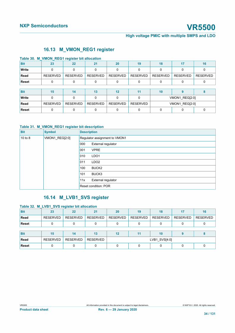
16.13 M_VMON_REG1 register
Table 30. M_VMON_REG1 register bit allocationBit 23 22 21 20 19 18 17 16
Write 0 0 0 0 0 0 0 0
Read RESERVED RESERVED RESERVED RESERVED RESERVED RESERVED RESERVED RESERVED
Reset 0 0 0 0 0 0 0 0
Bit 15 14 13 12 11 10 9 8
Write 0 0 0 0 0 VMON1_REG[2:0]
Read RESERVED RESERVED RESERVED RESERVED RESERVED VMON1_REG[2:0]
Reset 0 0 0 0 0 0 0 0
Table 31. M_VMON_REG1 register bit descriptionBit Symbol Description
Regulator assignment to VMON1
000 External regulator
001 VPRE
010 LDO1
011 LDO2
100 BUCK2
101 BUCK3
11x External regulator
10 to 8 VMON1_REG[2:0]
Reset condition: POR
16.14 M_LVB1_SVS register
Table 32. M_LVB1_SVS register bit allocationBit 23 22 21 20 19 18 17 16
Read RESERVED RESERVED RESERVED RESERVED RESERVED RESERVED RESERVED RESERVED
Reset 0 0 0 0 0 0 0 0
Bit 15 14 13 12 11 10 9 8
Read RESERVED RESERVED RESERVED LVB1_SVS[4:0]
Reset 0 0 0 0 0 0 0 0

NXP Semiconductors VR5500High voltage PMIC with multiple SMPS and LDO
VR5500 All information provided in this document is subject to legal disclaimers. © NXP B.V. 2020. All rights reserved.
Product data sheet Rev. 6 — 29 January 202035 / 131
Table 33. M_LVB1_SVS register bit descriptionBit Symbol Description
Static voltage scaling negative offset
00000 0 mV
00001 −6.25 mV
00010 −12.50 mV
00011 −18.75 mV
00100 −25 mV
00101 −31.25 mV
00110 −37.5 mV
00111 −43.75 mV
01000 −50 mV
01001 −56.25 mV
01010 −62.5 mV
01011 −68.75 mV
01100 −75 mV
01101 −81.25 mV
01110 −87.5 mV
01111 −93.75 mV
10000 −100 mV
12 to 8 LVB1_SVS[4:0]
Reset condition: POR
16.15 M_MEMORY0 register
Table 34. M_MEMORY0 register bit allocationBit 23 22 21 20 19 18 17 16
Write MEMORY0[15:8]
Read MEMORY0[15:8]
Reset 0 0 0 0 0 0 0 0
Bit 15 14 13 12 11 10 9 8
Write MEMORY0[7:0]
Read MEMORY0[7:0]
Reset 0 0 0 0 0 0 0 0
Table 35. M_MEMORY0 register bit descriptionBit Symbol Description
Free memory field for data storage
0...
...1
16 bits free memory
23 to 8 MEMORY0[15:0]
Reset condition: POR

NXP Semiconductors VR5500High voltage PMIC with multiple SMPS and LDO
VR5500 All information provided in this document is subject to legal disclaimers. © NXP B.V. 2020. All rights reserved.
Product data sheet Rev. 6 — 29 January 202036 / 131
16.16 M_MEMORY1 register
Table 36. M_MEMORY1 register bit allocationBit 23 22 21 20 19 18 17 16
Write MEMORY1[15:0]
Read MEMORY1[15:0]
Reset 0 0 0 0 0 0 0 0
Bit 15 14 13 12 11 10 9 8
Write MEMORY1[15:0]
Read MEMORY1[15:0]
Reset 0 0 0 0 0 0 0 0
Table 37. M_MEMORY1 register bit descriptionBit Symbol Description
Free memory field for data storage
0…
…1
16 bits free memory
23 to 8 MEMORY1[15:0]
Reset condition: POR
16.17 M_DEVICEID register
Table 38. M_DEVICEID register bit allocationBit 23 22 21 20 19 18 17 16
Read FMREV[3:0] MMREV[3:0]
Reset 0 0 1 1 0 0 0 0
Bit 15 14 13 12 11 10 9 8
Read DEVICEID[7:0]
Reset 0 0 0 0 0 0 0 0
Table 39. M_DEVICEID register bit descriptionBit Symbol Description
Full mask revision
Full mask revision configured by metal connection
23 to 20 FMREV[3:0]
Reset condition: POR
Metal Mask Revision
Metal mask revision configured by metal connection
19 to 16 MMREV[3:0]
Reset condition: POR
Device ID
x…x Device ID from OTP_DEVICEID[7:0] bits
15 to 8 DEVICEID[7:0]
Reset condition: POR
NXP Semiconductors VR5500High voltage PMIC with multiple SMPS and LDO
VR5500 All information provided in this document is subject to legal disclaimers. © NXP B.V. 2020. All rights reserved.
Product data sheet Rev. 6 — 29 January 202037 / 131
17 Fail-safe register mapping
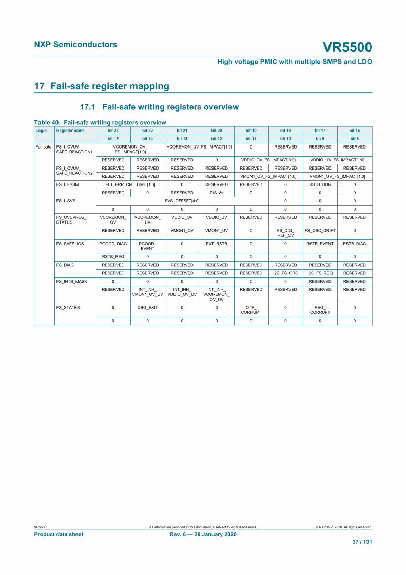
17.1 Fail-safe writing registers overview
Table 40. Fail-safe writing registers overviewbit 23 bit 22 bit 21 bit 20 bit 19 bit 18 bit 17 bit 16Logic Register name
bit 15 bit 14 bit 13 bit 12 bit 11 bit 10 bit 9 bit 8
VCOREMON_OV_FS_IMPACT[1:0]
VCOREMON_UV_FS_IMPACT[1:0] 0 RESERVED RESERVED RESERVEDFS_I_OVUV_SAFE_REACTION1
RESERVED RESERVED RESERVED 0 VDDIO_OV_FS_IMPACT[1:0] VDDIO_UV_FS_IMPACT[1:0]
RESERVED RESERVED RESERVED RESERVED RESERVED RESERVED RESERVED RESERVEDFS_I_OVUV_SAFE_REACTION2
RESERVED RESERVED RESERVED RESERVED VMON1_OV_FS_IMPACT[1:0] VMON1_UV_FS_IMPACT[1:0]
FLT_ERR_CNT_LIMIT[1:0] 0 RESERVED RESERVED 0 RSTB_DUR 0FS_I_FSSM
RESERVED 0 RESERVED DIS_8s 0 0 0 0
SVS_OFFSET[4:0] 0 0 0FS_I_SVS
0 0 0 0 0 0 0 0
VCOREMON_OV
VCOREMON_UV
VDDIO_OV VDDIO_UV RESERVED RESERVED RESERVED RESERVEDFS_OVUVREG_STATUS
RESERVED RESERVED VMON1_OV VMON1_UV 0 FS_DIG_REF_OV
FS_OSC_DRIFT 0
PGOOD_DIAG PGOOD_EVENT
0 EXT_RSTB 0 0 RSTB_EVENT RSTB_DIAGFS_SAFE_IOS
RSTB_REQ 0 0 0 0 0 0 0
RESERVED RESERVED RESERVED RESERVED RESERVED RESERVED RESERVED RESERVEDFS_DIAG
RESERVED RESERVED RESERVED RESERVED RESERVED I2C_FS_CRC I2C_FS_REQ RESERVED
0 0 0 0 0 0 RESERVED RESERVEDFS_INTB_MASK
RESERVED INT_INH_VMON1_OV_UV
INT_INH_VDDIO_OV_UV
INT_INH_VCOREMON_
OV_UV
RESERVED RESERVED RESERVED RESERVED
0 DBG_EXIT 0 0 OTP_CORRUPT
0 REG_CORRUPT
0
Fail-safe
FS_STATES
0 0 0 0 0 0 0 0

NXP Semiconductors VR5500High voltage PMIC with multiple SMPS and LDO
VR5500 All information provided in this document is subject to legal disclaimers. © NXP B.V. 2020. All rights reserved.
Product data sheet Rev. 6 — 29 January 202038 / 131
17.2 Fail-safe reading registers overview
Table 41. Fail-safe reading registers overviewbit 23 bit 22 bit 21 bit 20 bit 19 bit 18 bit 17 bit 16Logic Register name
bit 15 bit 14 bit 13 bit 12 bit 11 bit 10 bit 9 bit 8
FS_COM_G RESERVED FS_IO_G FS_REG_OVUV_G
RESERVED RESERVED RESERVED RESERVEDFS_GRL_FLAGS
RESERVED RESERVED RESERVED RESERVED RESERVED RESERVED RESERVED RESERVED
VCOREMON_OV_FS_IMPACT[1:0]
VCOREMON_UV_FS_IMPACT[1:0] RESERVED RESERVED RESERVED RESERVEDFS_I_OVUV_SAFE_REACTION1
RESERVED RESERVED RESERVED RESERVED VDDIO_OV_FS_IMPACT[1:0] VDDIO_UV_FS_IMPACT[1:0]
RESERVED RESERVED RESERVED RESERVED RESERVED RESERVED RESERVED RESERVEDFS_I_OVUV_SAFE_REACTION2
RESERVED RESERVED RESERVED RESERVED VMON1_OV_FS_IMPACT[1:0] VMON1_UV_FS_IMPACT[1:0]
FLT_ERR_CNT_LIMIT[1:0] RESERVED RESERVED RESERVED RESERVED RSTB_DUR RESERVEDFS_I_FSSM
RESERVED RESERVED RESERVED DIS_8s FLT_ERR_CNT[3:0]
SVS_OFFSET[4:0] RESERVED RESERVED RESERVEDFS_I_SVS
RESERVED RESERVED RESERVED RESERVED RESERVED RESERVED RESERVED RESERVED
VCOREMON_OV
VCOREMON_UV
VDDIO_OV VDDIO_UV RESERVED RESERVED RESERVED RESERVEDFS_OVUVREG_STATUS
RESERVED RESERVED VMON1_OV VMON1_UV RESERVED FS_DIG_REF_OV
FS_OSC_DRIFT RESERVED
PGOOD_DIAG PGOOD_EVENT
PGOOD_SNS EXT_RSTB RSTB_DRV RSTB_SNS RSTB_EVENT RSTB_DIAGFS_SAFE_IOS
RESERVED RESERVED RESERVED RESERVED RESERVED RESERVED RESERVED RESERVED
RESERVED RESERVED RESERVED RESERVED ERRMON RESERVED RESERVED RESERVEDFS_DIAG
RESERVED RESERVED RESERVED RESERVED RESERVED I2C_FS_CRC I2C_FS_REQ RESERVED
RESERVED RESERVED RESERVED RESERVED RESERVED RESERVED RESERVED RESERVEDFS_INTB_MASK
RESERVED INT_INH_VMON1_OV_UV
INT_INH_VDDIO_OV_UV
INT_INH_VCOREMON_
OV_UV
RESERVED RESERVED RESERVED RESERVED
RESERVED RESERVED DBG_MODE RESERVED OTP_CORRUPT
RESERVED REG_CORRUPT
RESERVED
Fail-safe
FS_STATES
RESERVED RESERVED RESERVED FSM_STATE[4:0]
17.3 FS_GRL_FLAGS register
Table 42. FS_GRL_FLAGS register bit allocationBit 23 22 21 20 19 18 17 16
Read FS_COM_G RESERVED FS_IO_G FS_REG_OVUV_G
RESERVED RESERVED RESERVED RESERVED
Reset 0 0 0 1 0 0 0 0
Bit 15 14 13 12 11 10 9 8
Read RESERVED RESERVED RESERVED RESERVED RESERVED RESERVED RESERVED RESERVED
Reset 0 0 0 0 0 0 0 0

NXP Semiconductors VR5500High voltage PMIC with multiple SMPS and LDO
VR5500 All information provided in this document is subject to legal disclaimers. © NXP B.V. 2020. All rights reserved.
Product data sheet Rev. 6 — 29 January 202039 / 131
Table 43. FS_GRL_FLAGS register bit descriptionBit Symbol Description
Report an issue in the communication (I2C)FS_COM_G = I2C_FS_CRC or I2C_FS_REQ
0 No failure
1 Failure
23 FS_COM_G
Reset condition: Real time information - cleared when all individual bits are cleared
Report an issue in one of the fail-safe IOsFS_IO_G = PGOOD_DIAG or RSTB_DIAG
0 No failure
1 Failure
21 FS_IO_G
Reset condition: real time information - cleared when all individual bits are cleared
Report an issue in one of the voltage monitoring (OV or UV)FS_REG_OVUV_G = VCOREMON_OV or VCOREMON_UV or VDDIO_OV or VDDIO_UV orVMON1_OV or VMON1_UV
0 No failure
1 Failure
20 FS_REG_OVUV_G
Reset condition: real time information - cleared when all individual bits are cleared
17.4 FS_I_OVUV_SAFE_REACTION1 register
Table 44. FS_I_OVUV_SAFE_REACTION1 register bit allocationBit 23 22 21 20 19 18 17 16
Write VCOREMON_OV_FS_IMPACT[1:0]
VCOREMON_UV_FS_IMPACT[1:0]
0 RESERVED RESERVED RESERVED
Read VCOREMON_OV_FS_IMPACT[1:0]
VCOREMON_UV_FS_IMPACT[1:0]
RESERVED RESERVED RESERVED RESERVED
Reset 1 1 0 1 0 0 0 0
Bit 15 14 13 12 11 10 9 8
Write RESERVED RESERVED RESERVED 0 VDDIO_OV_FS_IMPACT[1:0]
VDDIO_UV_FS_IMPACT[1:0]
Read RESERVED RESERVED RESERVED RESERVED VDDIO_OV_FS_IMPACT[1:0]
VDDIO_UV_FS_IMPACT[1:0]
Reset 0 0 0 0 1 1 0 1
Table 45. FS_I_OVUV_SAFE_REACTION1 register bit descriptionBit Symbol Description
23 to 22 VCOREMON_OV_FS_IMPACT[1:0] Table 87
21 to 20 VCOREMON_UV_FS_IMPACT[1:0] Table 87
11 to 10 VDDIO_OV_FS_IMPACT[1:0] Table 90
9 to 8 VDDIO_UV_FS_IMPACT[1:0] Table 90

NXP Semiconductors VR5500High voltage PMIC with multiple SMPS and LDO
VR5500 All information provided in this document is subject to legal disclaimers. © NXP B.V. 2020. All rights reserved.
Product data sheet Rev. 6 — 29 January 202040 / 131
17.5 FS_I_OVUV_SAFE_REACTION2 register
Table 46. FS_I_OVUV_SAFE_REACTION2 register bit allocationBit 23 22 21 20 19 18 17 16
Write RESERVED RESERVED RESERVED RESERVED RESERVED RESERVED RESERVED RESERVED
Read RESERVED RESERVED RESERVED RESERVED RESERVED RESERVED RESERVED RESERVED
Reset 1 1 0 1 1 1 0 1
Bit 15 14 13 12 11 10 9 8
Write RESERVED RESERVED RESERVED RESERVED VMON1_OV_FS_IMPACT[1:0]
VMON1_UV_FS_IMPACT[1:0]
Read RESERVED RESERVED RESERVED RESERVED VMON1_OV_FS_IMPACT[1:0]
VMON1_UV_FS_IMPACT[1:0]
Reset 1 1 0 1 1 1 0 1
Table 47. FS_I_OVUV_SAFE_REACTION2 register bit descriptionBit Symbol Description
11 to 10 VMON1_OV_FS_IMPACT[1:0]
9 to 8 VMON1_UV_FS_IMPACT[1:0]
See Table 92
17.6 FS_I_FSSM register
Table 48. FS_I_FSSM register bit allocationBit 23 22 21 20 19 18 17 16
Write FLT_ERR_CNT_LIMIT[1:0] 0 RESERVED RESERVED 0 RSTB_DUR 0
Read FLT_ERR_CNT_LIMIT[1:0] RESERVED RESERVED RESERVED RESERVED RSTB_DUR RESERVED
Reset 0 1 0 1 0 0 0 0
Bit 15 14 13 12 11 10 9 8
Write RESERVED 0 RESERVED DIS_8s 0 0 0 0
Read RESERVED RESERVED RESERVED DIS_8s FLT_ERR_CNT[3:0]
Reset 1 0 0 0 0 0 0 1
Table 49. FS_I_FSSM register bit descriptionBit Symbol Description
23 to 22 FLT_ERR_CNT_LIMIT[1:0] See Table 95
RSTB pulse duration configuration
0 10 ms
1 1.0 ms
17 RSTB_DUR
Reset condition: POR
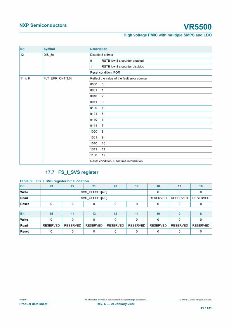
NXP Semiconductors VR5500High voltage PMIC with multiple SMPS and LDO
VR5500 All information provided in this document is subject to legal disclaimers. © NXP B.V. 2020. All rights reserved.
Product data sheet Rev. 6 — 29 January 202041 / 131
Bit Symbol Description
Disable 8 s timer
0 RSTB low 8 s counter enabled
1 RSTB low 8 s counter disabled
12 DIS_8s
Reset condition: POR
Reflect the value of the fault error counter
0000 0
0001 1
0010 2
0011 3
0100 4
0101 5
0110 6
0111 7
1000 8
1001 9
1010 10
1011 11
1100 12
11 to 8 FLT_ERR_CNT[3:0]
Reset condition: Real time information
17.7 FS_I_SVS register
Table 50. FS_I_SVS register bit allocationBit 23 22 21 20 19 18 17 16
Write SVS_OFFSET[4:0] 0 0 0
Read SVS_OFFSET[4:0] RESERVED RESERVED RESERVED
Reset 0 0 0 0 0 0 0 0
Bit 15 14 13 12 11 10 9 8
Write 0 0 0 0 0 0 0 0
Read RESERVED RESERVED RESERVED RESERVED RESERVED RESERVED RESERVED RESERVED
Reset 0 0 0 0 0 0 0 0

NXP Semiconductors VR5500High voltage PMIC with multiple SMPS and LDO
VR5500 All information provided in this document is subject to legal disclaimers. © NXP B.V. 2020. All rights reserved.
Product data sheet Rev. 6 — 29 January 202042 / 131
Table 51. FS_I_SVS register bit descriptionBit Symbol Description
Static voltage scaling negative offset
0 0000 0 mV
0 0001 −6.25 mV
0 0010 −12.50 mV
0 0011 −18.75 mV
0 0100 −25 mV
0 0101 −31.25 mV
0 0110 −37.5 mV
0 0111 −43.75 mV
0 1000 −50 mV
0 1001 −56.25 mV
0 1010 −62.5 mV
0 1011 −68.75 mV
0 1100 −75 mV
0 1101 −81.25 mV
0 1110 −87.5 mV
0 1111 −93.75 mV
1 0000 −100 mV
23 to 19 SVS_OFFSET[4:0]
Reset condition: POR
17.8 FS_OVUVREG_STATUS register
Table 52. FS_OVUVREG_STATUS register bit allocationBit 23 22 21 20 19 18 17 16
Write VCOREMON_OV
VCOREMON_UV
VDDIO_OV VDDIO_UV RESERVED RESERVED RESERVED RESERVED
Read VCOREMON_OV
VCOREMON_UV
VDDIO_OV VDDIO_UV RESERVED RESERVED RESERVED RESERVED
Reset 0 1 0 1 0 1 0 1
Bit 15 14 13 12 11 10 9 8
Write RESERVED RESERVED VMON1_OV VMON1_UV 0 FS_DIG_REF_OV
FS_OSC_DRIFT
0
Read RESERVED RESERVED VMON1_OV VMON1_UV RESERVED FS_DIG_REF_OV
FS_OSC_DRIFT
RESERVED
Reset 0 1 0 1 0 0 0 0
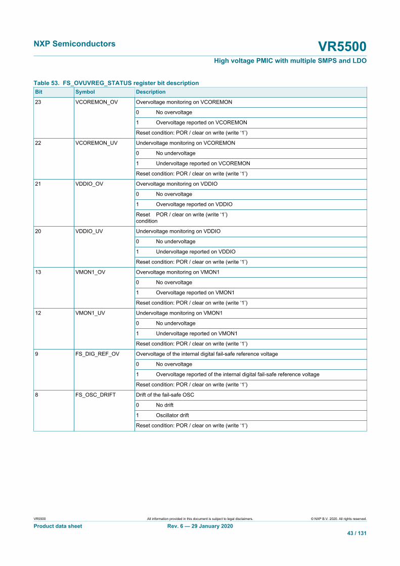
NXP Semiconductors VR5500High voltage PMIC with multiple SMPS and LDO
VR5500 All information provided in this document is subject to legal disclaimers. © NXP B.V. 2020. All rights reserved.
Product data sheet Rev. 6 — 29 January 202043 / 131
Table 53. FS_OVUVREG_STATUS register bit descriptionBit Symbol Description
Overvoltage monitoring on VCOREMON
0 No overvoltage
1 Overvoltage reported on VCOREMON
23 VCOREMON_OV
Reset condition: POR / clear on write (write ‘1’)
Undervoltage monitoring on VCOREMON
0 No undervoltage
1 Undervoltage reported on VCOREMON
22 VCOREMON_UV
Reset condition: POR / clear on write (write ‘1’)
Overvoltage monitoring on VDDIO
0 No overvoltage
1 Overvoltage reported on VDDIO
21 VDDIO_OV
Resetcondition
POR / clear on write (write ‘1’)
Undervoltage monitoring on VDDIO
0 No undervoltage
1 Undervoltage reported on VDDIO
20 VDDIO_UV
Reset condition: POR / clear on write (write ‘1’)
Overvoltage monitoring on VMON1
0 No overvoltage
1 Overvoltage reported on VMON1
13 VMON1_OV
Reset condition: POR / clear on write (write ‘1’)
Undervoltage monitoring on VMON1
0 No undervoltage
1 Undervoltage reported on VMON1
12 VMON1_UV
Reset condition: POR / clear on write (write ‘1’)
Overvoltage of the internal digital fail-safe reference voltage
0 No overvoltage
1 Overvoltage reported of the internal digital fail-safe reference voltage
9 FS_DIG_REF_OV
Reset condition: POR / clear on write (write ‘1’)
Drift of the fail-safe OSC
0 No drift
1 Oscillator drift
8 FS_OSC_DRIFT
Reset condition: POR / clear on write (write ‘1’)
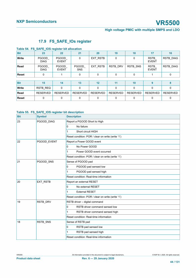
NXP Semiconductors VR5500High voltage PMIC with multiple SMPS and LDO
VR5500 All information provided in this document is subject to legal disclaimers. © NXP B.V. 2020. All rights reserved.
Product data sheet Rev. 6 — 29 January 202044 / 131
17.9 FS_SAFE_IOs register
Table 54. FS_SAFE_IOS register bit allocationBit 23 22 21 20 19 18 17 16
Write PGOOD_DIAG
PGOOD_EVENT
0 EXT_RSTB 0 0 RSTB_EVENT
RSTB_DIAG
Read PGOOD_DIAG
PGOOD_EVENT
PGOOD_SNS
EXT_RSTB RSTB_DRV RSTB_SNS RSTB_EVENT
RSTB_DIAG
Reset 0 1 0 0 0 0 1 0
Bit 15 14 13 12 11 10 9 8
Write RSTB_REQ 0 0 0 0 0 0 0
Read RESERVED RESERVED RESERVED RESERVED RESERVED RESERVED RESERVED RESERVED
Reset 0 0 0 0 0 0 0 0
Table 55. FS_SAFE_IOS register bit descriptionBit Symbol Description
Report a PGOOD Short to High
0 No failure
1 Short circuit HIGH
23 PGOOD_DIAG
Reset condition: POR / clear on write (write ‘1’)
Report a Power GOOD event
0 No Power GOOD
1 Power GOOD event occurred
22 PGOOD_EVENT
Reset condition: POR / clear on write (write ‘1’)
Sense of PGOOD pad
0 PGOOD pad sensed low
1 PGOOD pad sensed high
21 PGOOD_SNS
Reset condition: Real-time information
Report an external RESET
0 No external RESET
1 External RESET
20 EXT_RSTB
Reset condition: POR / clear on write (write ‘1’)
RSTB driver – digital command
0 RSTB driver command sensed low
1 RSTB driver command sensed high
19 RSTB_DRV
Reset condition: Real-time information
Sense of RSTB pad
0 RSTB pad sensed low
1 RSTB pad sensed high
18 RSTB_SNS
Reset condition: Real-time information

NXP Semiconductors VR5500High voltage PMIC with multiple SMPS and LDO
VR5500 All information provided in this document is subject to legal disclaimers. © NXP B.V. 2020. All rights reserved.
Product data sheet Rev. 6 — 29 January 202045 / 131
Bit Symbol Description
Report a RSTB event
0 No RESET
1 RESET occurred
17 RSTB_EVENT
Reset condition: POR / clear on write (write ‘1’)
Report a RSTB short to high
0 No failure
1 Short circuit high
16 RSTB_DIAG
Reset condition: POR / clear on write (write ‘1’)
Request assertion of RSTB (Pulse)
0 No assertion
1 RSTB assertion (pulse)
15 RSTB_REQ
Reset condition: POR
17.10 FS_DIAG register
Table 56. FS_DIAG register bit allocationBit 23 22 21 20 19 18 17 16
Write RESERVED RESERVED RESERVED RESERVED RESERVED RESERVED RESERVED RESERVED
Read RESERVED RESERVED RESERVED RESERVED RESERVED RESERVED RESERVED RESERVED
Reset 0 0 0 0 0 0 0 0
Bit 15 14 13 12 11 10 9 8
Write RESERVED RESERVED RESERVED RESERVED RESERVED I2C_FS_CRC I2C_FS_REQ RESERVED
Read RESERVED RESERVED RESERVED RESERVED RESERVED I2C_FS_CRC I2C_FS_REQ RESERVED
Reset 1 0 0 0 0 0 0 1
Table 57. FS_DIAG register bit descriptionBit Symbol Description
Invalid fail-safe I2C access (wrong write or read, write to INIT registers in normal mode, wrongaddress)
0 No error
1 I2C violation
10 I2C_FS_CRC
Reset condition: POR / clear on write (write ‘1’)
Fail-safe I2C communication CRC issue
0 No error
1 Error detected in the CRC
9 I2C_FS_REQ
Reset condition: POR / clear on write (write ‘1’)

NXP Semiconductors VR5500High voltage PMIC with multiple SMPS and LDO
VR5500 All information provided in this document is subject to legal disclaimers. © NXP B.V. 2020. All rights reserved.
Product data sheet Rev. 6 — 29 January 202046 / 131
17.11 FS_INTB_MASK register
Table 58. FS_INTB_MASK register bit allocationBit 23 22 21 20 19 18 17 16
Write 0 0 0 0 0 0 RESERVED RESERVED
Read RESERVED RESERVED RESERVED RESERVED RESERVED RESERVED RESERVED RESERVED
Reset 0 0 0 0 0 0 0 0
Bit 15 14 13 12 11 10 9 8
Write RESERVED INT_INH_VMON1_OV_UV
INT_INH_VDDIO_OV_UV
INT_INH_VCOREMON_
OV_UV
RESERVED RESERVED RESERVED RESERVED
Read RESERVED INT_INH_VMON1_OV_UV
INT_INH_VDDIO_OV_UV
INT_INH_VCOREMON_
OV_UV
RESERVED RESERVED RESERVED RESERVED
Reset 0 0 0 0 0 0 0 0
Table 59. FS_INTB_MASK register bit descriptionBit Symbol Description
Inhibit INTERRUPT on VMON1 OV and UV event
0 Interruption NOT MASKED
1 Interruption MASKED
14 INT_INH_VMON1_OV_UV
Reset condition: POR
Inhibit INTERRUPT on VDDIO OV and UV event
0 Interruption NOT MASKED
1 Interruption MASKED
13 INT_INH_VDDIO_OV_UV
Reset condition: POR
Inhibit INTERRUPT on VCOREMON OV and UV event
0 Interruption NOT MASKED
1 Interruption MASKED
12 INT_INH_VCOREMON_OV_UV
Reset condition: POR
17.12 FS_STATES register
Table 60. FS_STATES register bit allocationBit 23 22 21 20 19 18 17 16
Write 0 DBG_EXIT 0 0 OTP_CORRUPT
0 REG_CORRUPT
0
Read RESERVED RESERVED DBG_MODE RESERVED OTP_CORRUPT
RESERVED REG_CORRUPT
RESERVED
Reset 0 0 0 0 0 0 0 0
Bit 15 14 13 12 11 10 9 8
Write 0 0 0 0 0 0 0 0
Read RESERVED RESERVED RESERVED FSM_STATE[4:0]
Reset 0 0 0 0 0 1 1 0

NXP Semiconductors VR5500High voltage PMIC with multiple SMPS and LDO
VR5500 All information provided in this document is subject to legal disclaimers. © NXP B.V. 2020. All rights reserved.
Product data sheet Rev. 6 — 29 January 202047 / 131
Table 61. FS_STATES register bit descriptionBit Symbol Description
Leave DEBUG mode
0 No action
1 Leave DEBUG mode
22 DBG_EXIT
Reset condition: POR
DEBUG mode status
0 NOT in DEBUG mode
1 In DEBUG mode
21 DBG_MODE
Reset condition: Real-time information
OTP bits corruption detection (5 ms cyclic check)
0 No error
1 OTP CRC error detected
19 OTP_CORRUPT
Reset condition: POR / clear on write (write ‘1’)
INIT register corruption detection (real-time comparison)
0 No error
1 INIT register content error detected (mismatch between FS_I_Register / FS_I_NOT_Register)
167
REG_CORRUPT
Reset condition: POR / clear on write (write ‘1’)
Report fail-safe state machine current state
0 0110 INIT_FS
12 to 8 FSM_STATE[4:0]
Reset condition: Real-time information

NXP Semiconductors VR5500High voltage PMIC with multiple SMPS and LDO
VR5500 All information provided in this document is subject to legal disclaimers. © NXP B.V. 2020. All rights reserved.
Product data sheet Rev. 6 — 29 January 202048 / 131
18 OTP bits configuration
18.1 Overview
Table 62. Main OTP_REGISTERSLegend: bold — Regulator behavior in case of TSD, VPRE, and VBOOST slew rate parameters can be changed later byI2C.Name Address BIT7 BIT6 BIT5 BIT4 BIT3 BIT2 BIT1 BIT0
OTP_CFG_VPRE_1 14 0 0 VPREV[5:0]
OTP_CFG_VPRE_2 15 0 0 VPRESC[5:0]
OTP_CFG_VPRE_3 16 VPREILIM[1:0] 1 0 1 1 VPRESRHS[1:0]
OTP_CFG_BOOST_1 17 0 0 VPRE_MODE 0 VBSTV[3:0]
OTP_CFG_BOOST_2 18 BOOSTEN VBSTTONTIME[1:0] VBSTSC[4:0]
OTP_CFG_BOOST_3 19 0 0 0 0 0 1 VBSTSR[1:0]
OTP_CFG_BUCK1_1 1A VB1V[7:0]
OTP_CFG_BUCK1_2 1B 0 0 0 VB1INDOPT[1:0] VB1SWILIM[1:0] VB12MULTIPH
OTP_CFG_BUCK2_1 1C VB2V[7:0]
OTP_CFG_BUCK2_2 1D 0 VB2INDOPT[1:0] BUCK2EN VB2SWILIM[1:0] 0 0
OTP_CFG_BUCK3_1 1E BUCK3EN VB3INDOPT[1:0] VB3V[4:0]
OTP_CFG_BUCK3_2 1F VB2GMCOMP[2:0] VB1GMCOMP[2:0] VB3SWILIM[1:0]
OTP_CFG_LDO 20 LDO2ILIM LDO2V[2:0] LDO1ILIM LDO1V[2:0]
OTP_CFG_SEQ_1 21 0 0 VB2S[2:0] VB1S[2:0]
OTP_CFG_SEQ_2 22 0 0 LDO2S[2:0] LDO1S[2:0]
OTP_CFG_SEQ_3 23 DVS_BUCK12[1:0] DVS_BUCK3[1:0] Tslot 0 VB3S[2:0]
OTP_CFG_CLOCK_1 24 0 0 VPRE_ph[2:0] 1 0 0
OTP_CFG_CLOCK_2 25 0 0 BUCK1_ph[2:0] VBST_ph[2:0]
OTP_CFG_CLOCK_3 26 0 0 BUCK3_ph[2:0] BUCK2_ph[2:0]
OTP_CFG_CLOCK_4 27 BUCK3_clk_sel
BUCK2_clk_sel
BUCK1_clk_sel
VBST_clk_sel VPRE_clk_sel PLL_sel 0 1
OTP_CFG_SM_1 28 0 0 conf_TSD[5:0]
OTP_CFG_SM_2 29 0 0 0 VPRE_off_dly 1 1 PSYNC_CFG PSYNC_EN
OTP_CFG_VSUP_UV 2A 0 0 0 0 0 0 0 VSUPCFG
OTP_CFG_I2C 2B 0 0 0 0 M_I2CDEVADDR[3:0]
OTP_CFG_OV 2C 0 0 0 0 0 VDDIO_REG_ASSIGN[2:0]
OTP_CFG_DEVID 2D DeviceID[7:0]

NXP Semiconductors VR5500High voltage PMIC with multiple SMPS and LDO
VR5500 All information provided in this document is subject to legal disclaimers. © NXP B.V. 2020. All rights reserved.
Product data sheet Rev. 6 — 29 January 202049 / 131
Table 63. Fail-safe OTP_REGISTERSName Address BIT7 BIT6 BIT5 BIT4 BIT3 BIT2 BIT1 BIT0
OTP_CFG_UVOV_1 0A VCORE_V[7:0]
OTP_CFG_UVOV_2 0B VDDIOOVTH[3:0] VCOREOVTH[3:0]
OTP_CFG_UVOV_3 0C 0 0 VDDIO_V VCORE_SVS_CLAMP[4:0]
OTP_CFG_UVOV_4 0D 0 0 0 0 VMON1OVTH[3:0]
OTP_CFG_UVOV_5 0E 0 0 0 0 0 0 0 0
OTP_CFG_UVOV_6 0F VDDIOUVTH[3:0] VCOREUVTH[3:0]
OTP_CFG_UVOV_7 10 0 0 0 0 VMON1UVTH[3:0]
OTP_CFG_UVOV_8 11 0 0 0 0 0 0 0 0
OTP_CFG_PGOOD 12 0 PGOOD_RSTB
0 0 0 PGOOD_VMON1
PGOOD_VDDIO
PGOOD_VCORE
OTP_CFG_ABIST1 13 0 0 0 0 0 0 0 0
OTP_CFG_ASIL 14 1 0 0 0 0 0 0 VMON1_EN
OTP_CFG_I2C 15 0 0 0 0 FS_I2CDEVADDR[3:0]
OTP_CFG_DGLT_DUR_1 16 0 0 VCORE_UV_DGLT[1:0] VCORE_OV_DGLT
VDDIO_UV_DGLT[1:0] VDDIO_OV_DGLT
OTP_CFG_DGLT_DUR_2 17 0 0 0 0 0 VMON1_UV_DGLT[1:0] VMON1_OV_DGLT
18.2 Main OTP bit description
Table 64. Main OTP bit descriptionAddress Register Bit Symbol Value Description
VPRE output voltage
00 1111 3.3 V
01 0100 3.8 V
01 0111 4.1 V
14 OTP_CFG_VPRE_1 5 to 0 VPREV[5:0]
10 0000 5.0 V
VPRE slope compensation
00 0100 40 mV/µs
00 0101 50 mV/µs
00 0110 60 mV/μs
00 0111 70 mV/μs
00 1000 80 mV/µs
00 1001 90 mV/µs
00 1010 100 mV/μs
00 1110 140 mV/μs
01 0001 170 mV/μs
01 0100 200 mV/μs
15 OTP_CFG_VPRE_2 5 to 0 VPRESC[5:0]
01 1000 240 mV/μs

NXP Semiconductors VR5500High voltage PMIC with multiple SMPS and LDO
VR5500 All information provided in this document is subject to legal disclaimers. © NXP B.V. 2020. All rights reserved.
Product data sheet Rev. 6 — 29 January 202050 / 131
Address Register Bit Symbol Value Description
VPRE current limitationthreshold
00 50 mV
01 80 mV
10 120 mV
7 to 6 VPREILIM[1:0]
11 150 mV
VPRE low-side slew ratecontrol
3 to 2 VPRESRLS[1:0]
11 PU/PD/900 mA
VPRE high-side slew ratecontrol
00 PU/PD/130 mA
01 PU/PD/260 mA
10 PU/PD/520 mA
16 OTP_CFG_VPRE_3
1 to 0 VPRESRHS[1:0]
11 PU/PD/900 mA
VPRE mode (PWM, APS)
0 Force PWM for 455 kHzsetting
5 VPRE_MODE
1 Automatic Pulse Skipping(APS) for 2.2 MHz setting
VBOOST output voltage
0110 5.0 V
17 OTP_CFG_BOOST_1
3 to 0 VBSTV[3:0]
1101 5.74 V
BOOST enable
0 Disabled
7 BOOSTEN
1 Enabled
BOOST minimum ON time
00 60 ns
6 to 5 VBSTTONTIME[1:0]
01 50 ns
VBOOST slopecompensation
0 0110 160 mV/μs
0 1100 125 mV/μs
18 OTP_CFG_BOOST_2
4 to 0 VBSTSC[4:0]
0 1110 79 mV/μs
VBOOST low-side slew ratecontrol
10 300 V/μs
19 OTP_CFG_BOOST_3 1 to 0 VBSTSR[1:0]
11 500 V/μs

NXP Semiconductors VR5500High voltage PMIC with multiple SMPS and LDO
VR5500 All information provided in this document is subject to legal disclaimers. © NXP B.V. 2020. All rights reserved.
Product data sheet Rev. 6 — 29 January 202051 / 131
Address Register Bit Symbol Value Description
VBUCK1 output voltage
0100 0000 0.8 V
0100 0100 0.825 V
0101 0000 0.9 V
0101 1000 0.95 V
0110 0000 1.0 V
01100100 1.025 V
0110 0101 1.03125 V
0111 0000 1.1 V
1000 0000 1.2 V
1000 1000 1.25 V
1001 0000 1.3 V
1001 1000 1.35 V
1010 0000 1.4 V
1011 0000 1.5 V
1A OTP_CFG_BUCK1_1 7 to 0 VB1V[7:0]
1011 0001 1.8 V
BUCK1 inductor selection
00 1 μH
01 0.47 μH
4 to 3 VB1INDOPT[1:0]
10 1.5 μH
BUCK1 current limitation
01 Reserved
2 to 1 VB1SWILIM1:0]
11 4.5 A
VBUCK1 and VBUCK2multiphase operation enable
0 Disabled
1B OTP_CFG_BUCK1_2
0 VB12MULTIPH
1 Enabled

NXP Semiconductors VR5500High voltage PMIC with multiple SMPS and LDO
VR5500 All information provided in this document is subject to legal disclaimers. © NXP B.V. 2020. All rights reserved.
Product data sheet Rev. 6 — 29 January 202052 / 131
Address Register Bit Symbol Value Description
VBUCK2 output voltage
0100 0000 0.8 V
0100 0100 0.825 V
0101 0000 0.9 V
0101 1000 0.95 V
0110 0000 1.0 V
01100100 1.025 V
0110 0101 1.03125 V
0111 0000 1.1 V
1000 0000 1.2 V
1000 1000 1.25 V
1001 0000 1.3 V
1001 1000 1.35 V
1010 0000 1.4 V
1011 0000 1.5 V
1C OTP_CFG_BUCK2_1 7 to 0 VB2V[7:0]
1011 0001 1.8 V
BUCK2 inductor selection
00 1 μH
01 0.47 μH
6 to 5 VB2INDOPT[1:0]
10 1.5 μH
BUCK2 enable
0 Disabled
4 BUCK2EN
1 Enabled
BUCK2 current limitation
01 Reserved
1D OTP_CFG_BUCK2_2
3 to 2 VB2SWILIM[1:0]
11 4.5 A

NXP Semiconductors VR5500High voltage PMIC with multiple SMPS and LDO
VR5500 All information provided in this document is subject to legal disclaimers. © NXP B.V. 2020. All rights reserved.
Product data sheet Rev. 6 — 29 January 202053 / 131
Address Register Bit Symbol Value Description
BUCK3 enable
0 Disabled
7 BUCK3EN
1 Enabled
BUCK3 inductor selection
00 1 μH
01 0.47 μH
6 to 5 VB3INDOPT[1:0]
10 1.5 μH
VBUCK3 output voltage
0 0000 1.0 V
0 0001 1.1 V
0 0010 1.2 V
0 0011 1.25 V
0 0100 1.3 V
0 0101 1.35 V
0 0110 1.5 V
0 0111 1.6 V
0 1000 1.8 V
0 1110 2.3 V
1 0000 2.5 V
1 0001 2.8 V
1E OTP_CFG_BUCK3_1
4 to 0 VB3V[4:0]
1 0101 3.3 V
BUCK2 compensationnetwork
001 16.25 GM
010 32.5 GM
011 48.75 GM
100 65 GM
101 81.25 GM
7 to 5 VB2GMCOMP[2:0]
110 97.5 GM
BUCK1 compensationnetwork
001 16.25 GM
010 32.5 GM
011 48.75 GM
100 65 GM
101 81.25 GM
4 to 2 VB1GMCOMP[2:0]
110 97.5 GM
BUCK3 current limitation
01 2.6 A
1F OTP_CFG_BUCK3_2
1 to 0 VB3SWILIM[1:0]
11 4.5 A
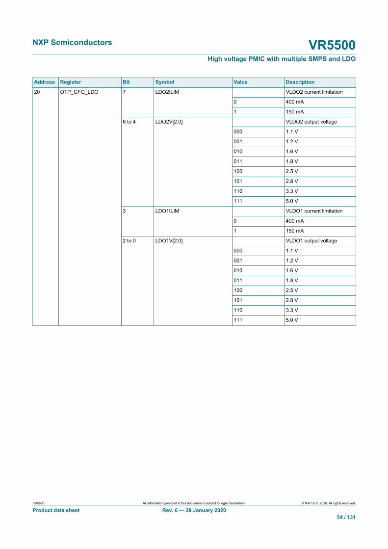
NXP Semiconductors VR5500High voltage PMIC with multiple SMPS and LDO
VR5500 All information provided in this document is subject to legal disclaimers. © NXP B.V. 2020. All rights reserved.
Product data sheet Rev. 6 — 29 January 202054 / 131
Address Register Bit Symbol Value Description
VLDO2 current limitation
0 400 mA
7 LDO2ILIM
1 150 mA
VLDO2 output voltage
000 1.1 V
001 1.2 V
010 1.6 V
011 1.8 V
100 2.5 V
101 2.8 V
110 3.3 V
6 to 4 LDO2V[2:0]
111 5.0 V
VLDO1 current limitation
0 400 mA
3 LDO1ILIM
1 150 mA
VLDO1 output voltage
000 1.1 V
001 1.2 V
010 1.6 V
011 1.8 V
100 2.5 V
101 2.8 V
110 3.3 V
20 OTP_CFG_LDO
2 to 0 LDO1V[2:0]
111 5.0 V

NXP Semiconductors VR5500High voltage PMIC with multiple SMPS and LDO
VR5500 All information provided in this document is subject to legal disclaimers. © NXP B.V. 2020. All rights reserved.
Product data sheet Rev. 6 — 29 January 202055 / 131
Address Register Bit Symbol Value Description
BUCK2 sequencing slot
000 Regulator start and stop inSlot 0
001 Regulator start and stop inSlot 1
010 Regulator start and stop inSlot 2
011 Regulator start and stop inSlot 3
100 Regulator start and stop inSlot 4
101 Regulator start and stop inSlot 5
110 Regulator start and stop inSlot 6
5 to 3 VB2S[2:0]
111 Regulator does not start(enabled by I2C)
BUCK1 sequencing slot
000 Regulator start and stop inSlot 0
001 Regulator start and stop inSlot 1
010 Regulator start and stop inSlot 2
011 Regulator start and stop inSlot 3
100 Regulator start and stop inSlot 4
101 Regulator start and stop inSlot 5
110 Regulator start and stop inSlot 6
21 OTP_CFG_SEQ_1
2 to 0 VB1S[2:0]
111 Regulator does not start(enabled by I2C)
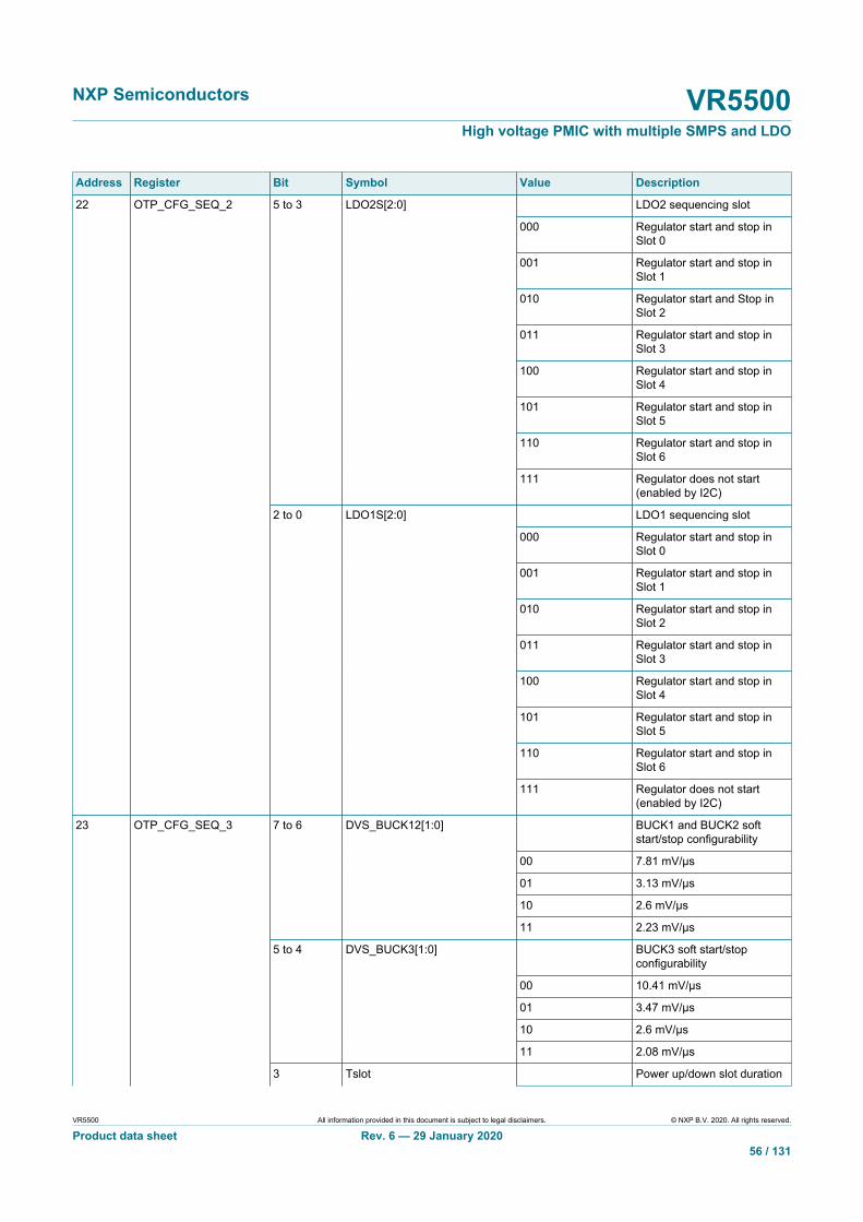
NXP Semiconductors VR5500High voltage PMIC with multiple SMPS and LDO
VR5500 All information provided in this document is subject to legal disclaimers. © NXP B.V. 2020. All rights reserved.
Product data sheet Rev. 6 — 29 January 202056 / 131
Address Register Bit Symbol Value Description
LDO2 sequencing slot
000 Regulator start and stop inSlot 0
001 Regulator start and stop inSlot 1
010 Regulator start and Stop inSlot 2
011 Regulator start and stop inSlot 3
100 Regulator start and stop inSlot 4
101 Regulator start and stop inSlot 5
110 Regulator start and stop inSlot 6
5 to 3 LDO2S[2:0]
111 Regulator does not start(enabled by I2C)
LDO1 sequencing slot
000 Regulator start and stop inSlot 0
001 Regulator start and stop inSlot 1
010 Regulator start and stop inSlot 2
011 Regulator start and stop inSlot 3
100 Regulator start and stop inSlot 4
101 Regulator start and stop inSlot 5
110 Regulator start and stop inSlot 6
22 OTP_CFG_SEQ_2
2 to 0 LDO1S[2:0]
111 Regulator does not start(enabled by I2C)
BUCK1 and BUCK2 softstart/stop configurability
00 7.81 mV/µs
01 3.13 mV/µs
10 2.6 mV/µs
7 to 6 DVS_BUCK12[1:0]
11 2.23 mV/µs
BUCK3 soft start/stopconfigurability
00 10.41 mV/µs
01 3.47 mV/µs
10 2.6 mV/µs
5 to 4 DVS_BUCK3[1:0]
11 2.08 mV/µs
23 OTP_CFG_SEQ_3
3 Tslot Power up/down slot duration

NXP Semiconductors VR5500High voltage PMIC with multiple SMPS and LDO
VR5500 All information provided in this document is subject to legal disclaimers. © NXP B.V. 2020. All rights reserved.
Product data sheet Rev. 6 — 29 January 202057 / 131
Address Register Bit Symbol Value Description
0 250 µs
1 1.0 ms
BUCK3 sequencing slot
000 Regulator start and stop inSlot 0
001 Regulator start and stop inSlot 1
010 Regulator start and Stop inSlot 2
011 Regulator start and stop inSlot 3
100 Regulator start and stop inSlot 4
101 Regulator start and stop inSlot 5
110 Regulator start and stop inSlot 6
2 to 0 VB3S[2:0]
111 Regulator does not start(enabled by I2C)
VPRE phase (delay)selection
000 no delay
001 delay 1
010 delay 2
011 delay 3
100 delay 4
101 delay 5
110 delay 6
24 OTP_CFG_CLOCK_1 5 to 3 VPRE_ph[2:0]
111 delay 7

NXP Semiconductors VR5500High voltage PMIC with multiple SMPS and LDO
VR5500 All information provided in this document is subject to legal disclaimers. © NXP B.V. 2020. All rights reserved.
Product data sheet Rev. 6 — 29 January 202058 / 131
Address Register Bit Symbol Value Description
VBUCK1 phase (delay)selection
000 no delay
001 delay 1
010 delay 2
011 delay 3
100 delay 4
101 delay 5
110 delay 6
5 to 3 BUCK1_ph[2:0]
111 delay 7
VBOOST phase (delay)selection
000 no delay
001 delay 1
010 delay 2
011 delay 3
100 delay 4
101 delay 5
110 delay 6
25 OTP_CFG_CLOCK_2
2 to 0 VBST_ph[2:0]
111 delay 7
VBUCK3 phase (delay)selection
000 no delay
001 delay 1
010 delay 2
011 delay 3
100 delay 4
101 delay 5
110 delay 6
5 to 3 BUCK3_ph[2:0]
111 delay 7
VBUCK2 phase (delay)selection
000 no delay
001 delay 1
010 delay 2
011 delay 3
100 delay 4
101 delay 5
110 delay 6
26 OTP_CFG_CLOCK_3
2 to 0 BUCK2_ph[2:0]
111 delay 7

NXP Semiconductors VR5500High voltage PMIC with multiple SMPS and LDO
VR5500 All information provided in this document is subject to legal disclaimers. © NXP B.V. 2020. All rights reserved.
Product data sheet Rev. 6 — 29 January 202059 / 131
Address Register Bit Symbol Value Description
BUCK3 clock selection7 BUCK3_clk_sel
0 CLK_DIV1 = 2.22 MHz
BUCK2 clock selection6 BUCK2_clk_sel
0 CLK_DIV1 = 2.22 MHz
BUCK1 clock selection5 BUCK1_clk_sel
0 CLK_DIV1 = 2.22 MHz
VBOOST clock selection4 VBST_clk_sel
0 CLK_DIV1 = 2.22 MHz
VPRE clock selection
0 CLK_DIV1 = 2.22 MHz
3 VPRE_clk_sel
1 CLK_DIV2 = 455 kHz
PLL enable
0 Disabled
27 OTP_CFG_CLOCK_4
2 PLL_sel
1 Enabled
BOOST behavior in case ofTSD
0 BOOST shutdown
conf_TSD[5]
1 BOOST shutdown + DFS
BUCK1 behavior in case ofTSD
0 BUCK1 shutdown
conf_TSD[4]
1 BUCK1 shutdown + DFS
BUCK2 behavior in case ofTSD
0 BUCK2 shutdown
conf_TSD[3]
1 BUCK2 shutdown + DFS
BUCK3 behavior in case ofTSD
0 BUCK3 shutdown
conf_TSD[2]
1 BUCK3 Shutdown + DFS
LDO1 behavior in case ofTSD
0 LDO1 shutdown
conf_TSD[1]
1 LDO1 shutdown + DFS
LDO2 behavior in case ofTSD
0 LDO2 shutdown
28 OTP_CFG_SM_1 5 to 0
conf_TSD[0]
1 LDO2 shutdown + DFS

NXP Semiconductors VR5500High voltage PMIC with multiple SMPS and LDO
VR5500 All information provided in this document is subject to legal disclaimers. © NXP B.V. 2020. All rights reserved.
Product data sheet Rev. 6 — 29 January 202060 / 131
Address Register Bit Symbol Value Description
Delay to turn OFF VPRE atdevice power down
0 250 μs
4 VPRE_off_dly
1 32 ms
Power up synchronization
0 2x VR5500
1 PSYNC_CFG
1 1x VR5500 and 1x externalPMIC
Synchronization with twodevices
0 Disabled
29 OTP_CFG_SM_2
0 PSYNC_EN
1 Enabled
VSUP undervoltagethreshold configuration
0 4.9 V for Vpre < 4.5 V
2A OTP_CFG_VSUP_UV 0 VSUP_CFG
1 6.2 V for Vpre > 4.5 V
Device I2C address
0000 Address D0
… ...
2B OTP_CFG_I2C 3 to 0 M_I2CDEVADDR[3:0]
1111 Address D15
Regulator assigned toVDDIO
000 External regulator
001 VPRE
010 LDO1
011 LDO2
100 BUCK3
101 External regulator
110 External regulator
2C OTP_CFG_OV 2 to 0 VDDIO_REG_ASSIGN[2:0]
111 External regulator
2D OTP_CFG_DEVID 7 to 0 DeviceID[7:0] Device ID

NXP Semiconductors VR5500High voltage PMIC with multiple SMPS and LDO
VR5500 All information provided in this document is subject to legal disclaimers. © NXP B.V. 2020. All rights reserved.
Product data sheet Rev. 6 — 29 January 202061 / 131
18.3 Fail-safe OTP bit description
Table 65. Fail-safe OTP bit descriptionAddress Register Bit Symbol Value Description
VCORE (VBUCK1) monitoring voltage
0100 0000 0.8 V
0100 0100 0.825 V
0101 0000 0.9 V
0101 1000 0.95 V
0110 0000 1 V
01100100 1.025 V
0110 0101 1.03125 V
0110 0000 1.1 V
1000 0000 1.2 V
1000 1000 1.25 V
1001 0000 1.3 V
1001 1000 1.35 V
1010 0000 1.4 V
1011 0000 1.5 V
0A OTP_CFG_UVOV_1 7 to 0 VCORE_V[7:0]
1011 0001 1.8 V

NXP Semiconductors VR5500High voltage PMIC with multiple SMPS and LDO
VR5500 All information provided in this document is subject to legal disclaimers. © NXP B.V. 2020. All rights reserved.
Product data sheet Rev. 6 — 29 January 202062 / 131
Address Register Bit Symbol Value Description
VDDIO overvoltage threshold configuration
0000 104.5 %
0001 105 %
0010 105.5 %
0011 106 %
0100 106.5 %
0101 107 %
0110 107.5
0111 108 %
1000 108.5 %
1001 109 %
1010 109.5 %
1011 110 %
1100 110.5 %
1101 111 %
1110 111.5 %
7 to 4 VDDIOOVTH[3:0]
1111 112 %
VCOREMON overvoltage thresholdconfiguration
0000 104.5 %
0001 105 %
0010 105.5 %
0011 106 %
0100 106.5 %
0101 107 %
0110 107.5
0111 108 %
1000 108.5 %
1001 109 %
1010 109.5 %
1011 110 %
1100 110.5 %
1101 111 %
1110 111.5 %
0B OTP_CFG_UVOV_2
3 to 0 VCOREOVTH[3:0]
1111 112 %
VDDIO voltage selection
0 3.3 V
5 VDDIO_V
1 5 V
SVS max value allowed (mask)
00000 2 steps available (−12.5 mV)
0C OTP_CFG_UVOV_3
4 to 0 VCORE_SVS_CLAMP[4:0]
00001 4 steps available (−25 mV)

NXP Semiconductors VR5500High voltage PMIC with multiple SMPS and LDO
VR5500 All information provided in this document is subject to legal disclaimers. © NXP B.V. 2020. All rights reserved.
Product data sheet Rev. 6 — 29 January 202063 / 131
Address Register Bit Symbol Value Description
00011 8 steps available (−50 mV)
00100 16 steps available (−100 mV)
VMON1 overvoltage threshold configuration
0000 104.5 %
0001 105 %
0010 105.5 %
0011 106 %
0100 106.5 %
0101 107 %
0110 107.5
0111 108 %
1000 108.5 %
1001 109 %
1010 109.5 %
1011 110 %
1100 110.5 %
1101 111 %
1110 111.5 %
0D OTP_CFG_UVOV_4 3 to 0 VMON1OVTH[3:0]
1111 112 %

NXP Semiconductors VR5500High voltage PMIC with multiple SMPS and LDO
VR5500 All information provided in this document is subject to legal disclaimers. © NXP B.V. 2020. All rights reserved.
Product data sheet Rev. 6 — 29 January 202064 / 131
Address Register Bit Symbol Value Description
VDDIO undervoltage threshold configuration
0000 95.5 %
0001 95 %
0010 94.5 %
0011 94 %
0100 93.5 %
0101 93 %
0110 92.5 %
0111 92 %
1000 91.5 %
1001 91 %
1010 90.5 %
1011 90 %
1100 89.5 %
1101 89 %
1110 88.5 %
7 to 4 VDDIOUVTH[3:0]
1111 88 %
VCOREMON undervoltage thresholdconfiguration
0000 95.5 %
0001 95 %
0010 94.5 %
0011 94 %
0100 93.5 %
0101 93 %
0110 92.5 %
0111 92 %
1000 91.5 %
1001 91 %
1010 90.5 %
1011 90 %
1100 89.5 %
1101 89 %
1110 88.5 %
0F OTP_CFG_UVOV_6
3 to 0 VCOREUVTH[3:0]
1111 88 %

NXP Semiconductors VR5500High voltage PMIC with multiple SMPS and LDO
VR5500 All information provided in this document is subject to legal disclaimers. © NXP B.V. 2020. All rights reserved.
Product data sheet Rev. 6 — 29 January 202065 / 131
Address Register Bit Symbol Value Description
VMON1 undervoltage threshold configuration
0000 95.5 %
0001 95 %
0010 94.5 %
0011 94 %
0100 93.5 %
0101 93 %
0110 92.5 %
0111 92 %
1000 91.5 %
1001 91 %
1010 90.5 %
1011 90 %
1100 89.5 %
1101 89 %
1110 88.5 %
10 OTP_CFG_UVOV_7 3 to 0 VMON1UVTH[3:0]
1111 88 %
RSTB assignment to PGOOD
0 Not assigned
6 PGOOD_RSTB
1 Assigned
VMON1 assignment to PGOOD
0 Not assigned
2 PGOOD_VMON1
1 Assigned
VDDIO assignment to PGOOD
0 Not assigned
1 PGOOD_VDDIO
1 Assigned
VCORE (BUCK1) assignment to PGOOD
0 Not assigned
12 OTP_CFG_PGOOD
0 PGOOD_VCORE
1 Assigned
VMON1 monitoring enable
0 Disabled
14 OTP_CFG_ASIL 0 VMON1_EN
1 Enabled
Device I2C address
0000 Address D0
… …
15 OTP_CFG_I2C 3 to 0 FS_I2CDEVADDR[3:0]
1111 Address D15

NXP Semiconductors VR5500High voltage PMIC with multiple SMPS and LDO
VR5500 All information provided in this document is subject to legal disclaimers. © NXP B.V. 2020. All rights reserved.
Product data sheet Rev. 6 — 29 January 202066 / 131
Address Register Bit Symbol Value Description
VCORE undervoltage filtering time
00 5 μs
01 15 μs
10 25 μs
5 to 4 VCORE_UV_DGLT[1:0]
11 40 μs
VCORE overvoltage filtering time
0 25 μs
3 VCORE_OV_DGLT
1 45 μs
VDDIO undervoltage filtering time
00 5 μs
01 15 μs
10 25 μs
2 to 1 VDDIO_UV_DGLT[1:0]
11 40 μs
VDDIO overvoltage filtering time
0 25 μs
16 OTP_CFG_DGLT_DUR_1
0 VDDIO_OV_DGLT
1 45 μs
VMON1 undervoltage filtering time
00 5 μs
01 15 μs
10 25 μs
2 to 1 VMON1_UV_DGLT[1:0]
11 40 μs
VMON1 overvoltage filtering time
0 25 μs
17 OTP_CFG_DGLT_DUR_2
0 VMON1_OV_DGLT
1 45 μs
19 Best of supply
19.1 Functional descriptionVBOS regulator manages the best of supply from VSUP, VPRE, and VBOOST toefficiently generate 5.0 V output to supply the internal biasing of the device. VBOS isalso the supply of VPRE high-side and low-side gate drivers and VBOOST low-side gatedriver.
VBOS undervoltage may not guarantee the full functionality of the device. Consequently,VBOS_UVL detection powers down the device.
VSUP_UV7 undervoltage threshold is used to enable the path from VSUP to VBOS whenVSUP < VSUP_UV7 to have a low drop path from VSUP, while VPRE is going low and topower up the device when VPRE is not started. When VSUP > VSUP_UV7, VBOS is forcedto use either VPRE or VBOOST to optimize the efficiency.
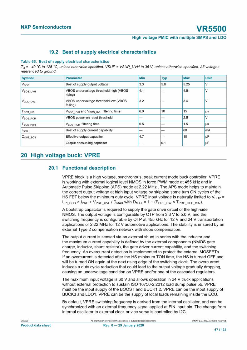
NXP Semiconductors VR5500High voltage PMIC with multiple SMPS and LDO
VR5500 All information provided in this document is subject to legal disclaimers. © NXP B.V. 2020. All rights reserved.
Product data sheet Rev. 6 — 29 January 202067 / 131
19.2 Best of supply electrical characteristics
Table 66. Best of supply electrical characteristicsTA = –40 °C to 125 °C, unless otherwise specified. VSUP = VSUP_UVH to 36 V, unless otherwise specified. All voltagesreferenced to ground.
Symbol Parameter Min Typ Max Unit
VBOS Best of supply output voltage 3.3 5.0 5.25 V
VBOS_UVH VBOS undervoltage threshold high (VBOSrising)
4.1 — 4.5 V
VBOS_UVL VBOS undervoltage threshold low (VBOSfalling)
3.2 — 3.4 V
TBOS_UV VBOS_UVH and VBOS_UVL filtering time 6.0 10 15 μs
VBOS_POR VBOS power-on reset threshold — — 2.5 V
TBOS_POR VBOS_POR filtering time 0.5 — 1.5 μs
IBOS Best of supply current capability — — 60 mA
Effective output capacitor 4.7 — 10 µFCOUT_BOS
Output decoupling capacitor — 0.1 — µF
20 High voltage buck: VPRE
20.1 Functional descriptionVPRE block is a high voltage, synchronous, peak current mode buck controller. VPREis working with external logical level NMOS in force PWM mode at 455 kHz and inAutomatic Pulse Skipping (APS) mode at 2.22 MHz . The APS mode helps to maintainthe correct output voltage at high input voltage by skipping some turn ON cycles of theHS FET below the minimum duty cycle. VPRE input voltage is naturally limited to VSUP =LPI_DCR × IPRE + VPRE_UVL / DMAX with DMAX = 1 − (FPRE_SW × TPRE_OFF_MIN).
A bootstrap capacitor is required to supply the gate drive circuit of the high-sideNMOS. The output voltage is configurable by OTP from 3.3 V to 5.0 V, and theswitching frequency is configurable by OTP at 455 kHz for 12 V and 24 V transportationapplications or 2.22 MHz for 12 V automotive applications. The stability is ensured by anexternal Type 2 compensation network with slope compensation.
The output current is sensed via an external shunt in series with the inductor andthe maximum current capability is defined by the external components (NMOS gatecharge, inductor, shunt resistor), the gate driver current capability, and the switchingfrequency. An overcurrent detection is implemented to protect the external MOSFETs.If an overcurrent is detected after the HS minimum TON time, the HS is turned OFF andwill be turned ON again at the next rising edge of the switching clock. The overcurrentinduces a duty cycle reduction that could lead to the output voltage gradually dropping,causing an undervoltage condition on VPRE and/or one of the cascaded regulators.
The maximum input voltage is 60 V and allows operation in 24 V truck applicationswithout external protection to sustain ISO 16750-2:2012 load dump pulse 5b. VPREmust be the input supply of the BOOST and BUCK1,2. VPRE can be the input supply ofBUCK3 and LDO1. VPRE can be the supply of local loads remaining inside the ECU.
By default, VPRE switching frequency is derived from the internal oscillator, and can besynchronized with an external frequency signal applied at FIN input pin. The change frominternal oscillator to external clock or vice versa is controlled by I2C.
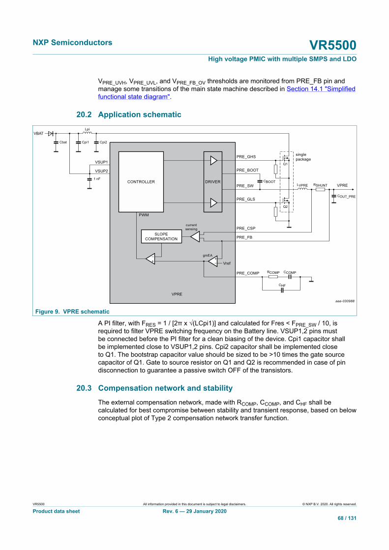
NXP Semiconductors VR5500High voltage PMIC with multiple SMPS and LDO
VR5500 All information provided in this document is subject to legal disclaimers. © NXP B.V. 2020. All rights reserved.
Product data sheet Rev. 6 — 29 January 202068 / 131
VPRE_UVH, VPRE_UVL, and VPRE_FB_OV thresholds are monitored from PRE_FB pin andmanage some transitions of the main state machine described in Section 14.1 "Simplifiedfunctional state diagram".
20.2 Application schematic
SLOPECOMPENSATION
PWM
Lpi
Cpi2Cpi1Cbat
VSUP1
VBAT
VSUP2
aaa-030988
currentsensing
gmEA
DRIVER
PRE_GHS
PRE_BOOT
PRE_SW
PRE_GLS
PRE_COMP
PRE_CSP
PRE_FB
Vref
singlepackage
VPRE
Q1
Q2
COUT_PRE
RSHUNTLVPRECBOOT
RCOMP CCOMP
CHF
CONTROLLER
VPRE
1 nF
Figure 9. VPRE schematic
A PI filter, with FRES = 1 / [2π x √(LCpi1)] and calculated for Fres < FPRE_SW / 10, isrequired to filter VPRE switching frequency on the Battery line. VSUP1,2 pins mustbe connected before the PI filter for a clean biasing of the device. Cpi1 capacitor shallbe implemented close to VSUP1,2 pins. Cpi2 capacitor shall be implemented closeto Q1. The bootstrap capacitor value should be sized to be >10 times the gate sourcecapacitor of Q1. Gate to source resistor on Q1 and Q2 is recommended in case of pindisconnection to guarantee a passive switch OFF of the transistors.
20.3 Compensation network and stabilityThe external compensation network, made with RCOMP, CCOMP, and CHF shall becalculated for best compromise between stability and transient response, based on belowconceptual plot of Type 2 compensation network transfer function.
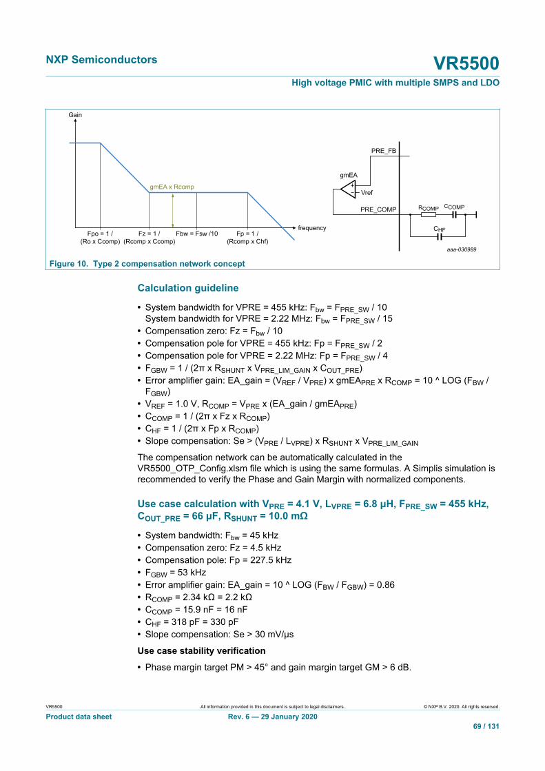
NXP Semiconductors VR5500High voltage PMIC with multiple SMPS and LDO
VR5500 All information provided in this document is subject to legal disclaimers. © NXP B.V. 2020. All rights reserved.
Product data sheet Rev. 6 — 29 January 202069 / 131
aaa-030989
PRE_COMP
Vref
gmEA
frequency
Gain
gmEA x Rcomp
Fz = 1 /(Rcomp x Ccomp)
Fpo = 1 /(Ro x Ccomp)
Fp = 1 /(Rcomp x Chf)
Fbw = Fsw /10
RCOMP CCOMP
CHF
PRE_FB
Figure 10. Type 2 compensation network concept
Calculation guideline
• System bandwidth for VPRE = 455 kHz: Fbw = FPRE_SW / 10System bandwidth for VPRE = 2.22 MHz: Fbw = FPRE_SW / 15
• Compensation zero: Fz = Fbw / 10• Compensation pole for VPRE = 455 kHz: Fp = FPRE_SW / 2• Compensation pole for VPRE = 2.22 MHz: Fp = FPRE_SW / 4• FGBW = 1 / (2π x RSHUNT x VPRE_LIM_GAIN x COUT_PRE)• Error amplifier gain: EA_gain = (VREF / VPRE) x gmEAPRE x RCOMP = 10 ^ LOG (FBW /
FGBW)• VREF = 1.0 V, RCOMP = VPRE x (EA_gain / gmEAPRE)• CCOMP = 1 / (2π x Fz x RCOMP)• CHF = 1 / (2π x Fp x RCOMP)• Slope compensation: Se > (VPRE / LVPRE) x RSHUNT x VPRE_LIM_GAIN
The compensation network can be automatically calculated in theVR5500_OTP_Config.xlsm file which is using the same formulas. A Simplis simulation isrecommended to verify the Phase and Gain Margin with normalized components.
Use case calculation with VPRE = 4.1 V, LVPRE = 6.8 μH, FPRE_SW = 455 kHz,COUT_PRE = 66 μF, RSHUNT = 10.0 mΩ
• System bandwidth: Fbw = 45 kHz• Compensation zero: Fz = 4.5 kHz• Compensation pole: Fp = 227.5 kHz• FGBW = 53 kHz• Error amplifier gain: EA_gain = 10 ^ LOG (FBW / FGBW) = 0.86• RCOMP = 2.34 kΩ = 2.2 kΩ• CCOMP = 15.9 nF = 16 nF• CHF = 318 pF = 330 pF• Slope compensation: Se > 30 mV/μs
Use case stability verification
• Phase margin target PM > 45° and gain margin target GM > 6 dB.

NXP Semiconductors VR5500High voltage PMIC with multiple SMPS and LDO
VR5500 All information provided in this document is subject to legal disclaimers. © NXP B.V. 2020. All rights reserved.
Product data sheet Rev. 6 — 29 January 202070 / 131
aaa-030990
-71.08028
71.077183
-3.10028 m
REFfrequency (Hz)10 106105102 104103
-45
0
-90
45
90phase
(°)
-135
-40
60
40
20
0
-20
100
80Gain(dB)
PM = 71°
-12.16019
-37.7993 m
-12.19798
REFfrequency (Hz)10 106105102 104103
-45
0
-90
45
90phase
(°)
-135
-40
60
40
20
0
-20
100
80Gain(dB)
GM = 12 dB
Figure 11. Phase and gain margin simulation
Use case transient response verification

NXP Semiconductors VR5500High voltage PMIC with multiple SMPS and LDO
VR5500 All information provided in this document is subject to legal disclaimers. © NXP B.V. 2020. All rights reserved.
Product data sheet Rev. 6 — 29 January 202071 / 131
aaa-030991
4.1
4.0
4.2
4.3
VOUT(V)
3.9
time (ms) 200 µs / div0 1.00.80.4 0.60.2
1.0
2.0
3.0
4.0
I_OUT(A)
0
load step from 1 A to 3 A300 mA / µs
257.0194 µs 508.2793 µs251.2599 µs
REF A
min UV - 84 mV
max OV + 84 mV
167.3434 mV
4.1830110
4.0156676
Figure 12. Transient response simulation
20.4 VPRE electrical characteristics
Table 67. VPRE electrical characteristicsTA = −40 °C to 125 °C, unless otherwise specified. VSUP = VSUP_UVH to 36 V, unless otherwise specified. All voltagesreferenced to ground.
Symbol Parameter Min Typ Max Unit
3.2 3.3 3.4 V
3.68 3.8 3.92 V
3.98 4.1 4.22 V
VPRE Output voltage (OTP_VPREV[5:0] bits)
4.85 5.0 5.15 V
Output voltage from 10 % to 90 % 250 450 650 μsVPRE_SOFT_START
Digital DAC soft start completion — — 1.35 ms
VPRE_STARTUP Overshoot at startup — — 3 %
VPRE_FB_OV Over voltage threshold protection 5.5 6.0 6.5 V
TPRE_FB_OV VPRE_FB_OV filtering time 1 2 3 μs

NXP Semiconductors VR5500High voltage PMIC with multiple SMPS and LDO
VR5500 All information provided in this document is subject to legal disclaimers. © NXP B.V. 2020. All rights reserved.
Product data sheet Rev. 6 — 29 January 202072 / 131
Symbol Parameter Min Typ Max Unit
VPRE_UVH Under voltage threshold high 2.9 — 3.1 V
VPRE_UVL Under voltage threshold low 2.5 — 2.7 V
TPRE_UV VPRE_UVH and VPRE_UVL filtering time 6.0 10 15 μs
430 455 480 kHzFPRE_SW Switching frequency range (OTP_VPRE_clk_selbit)
2.1 2.22 2.35 MHz
Typical inductor value for FPRE_SW = 455 kHz 4.7 6.8 10 μHLVPRE
Typical inductor value for FPRE_SW = 2.22 MHz 1.5 2.2 4.7 µH
VPRE_LOAD_REG_455k Transient load regulation at 455 kHzVSUP = 6.0 V to 36 V(LVPRE = 6.8 µH, COUT_PRE = 66 μF, from 1.0 Ato 3.0 A, di/dt = 300 mA/μs)
−3 — 3 %
VPRE_LOAD_REG_2.2M Transient load regulation at 2.22 MHzVSUP = 6.0 V to 18 V(LVPRE = 2.2 µH, COUT_PRE = 44 μF, from 1.0 Ato 3.0 A, di/dt = 300 mA/μs)
−3 — 3 %
VPRE_LINE_REG_455k Transient line regulation at 455 kHzVSUP = 6.0 V to 18 V and VSUP = 12 V to 36 V(Cin = 47 µF + PI filter, LVPRE = 6.8 µH,COUT_PRE = 66 μF, dv/dt = 100 mV/μs)
−3 — 3 %
VPRE_LINE_REG_2.2M Transient line regulation at 2.22 MHzVSUP = 6.0 V to 18 V(Cin = 47 µF + PI filter, LVPRE = 2.2 µH,COUT_PRE = 44 μF, dv/dt = 100 mV/μs)
−3 — 3 %
VPRE_RIPPLE_455k Ripple at 455 kHzVSUP = 12 V and VSUP = 24 V(LVPRE = 6.8 µH, COUT_PRE = 66 μF, VPRE = 3.3V and 5.0 V, IPRE = 4A)
−1 — 1 %
VPRE_RIPPLE_2.2M Ripple at 2.22 MHzVSUP = 12 V(LVPRE = 2.2 µH, COUT_PRE = 44 μF, VPRE = 3.3V and 5.0 V, IPRE = 2A)
−0.5 — 0.5 %
TPRE_ON_MIN HS minimum ON time 15 25 35 ns
TPRE_OFF_MIN HS minimum OFF time 20 40 60 ns
RSHUNT Current sense resistor (±1 %) 10 — 20 mΩ
VPRE_LIM_GAIN Current sense amplifier gain 4.5 5 5.5
37 50 63 mV
60.8 80 99.2 mV
93.6 120 146.4 mV
VPRE_LIM_TH1 Current sense amplifier peak detectionthreshold(OTP_VPREILIM[1:0] bits) Note: 150 mV settingis not available for 2.22 MHz
117 150 183 mV
ILIM_PRE = VPRE_LIM_TH / RSHUNTInductor peak current limitation range (RSHUNT =10 mΩ, VPRE_LIM_TH1 = 50 mV)
3.75 5 6.25 AILIM_PRE
Inductor peak current limitation range (RSHUNT =10 mΩ, VPRE_LIM_TH1 = 150 mV)To be recalculated for different RSHUNT anddifferent VPRE_LIM_TH
12 15 18 A
VPRE_DRV HS and LS gate driver output voltage — VBOS — V
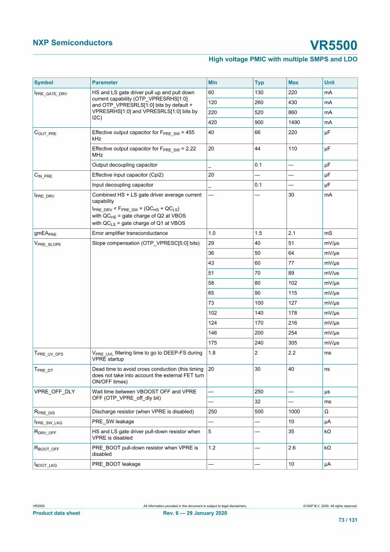
NXP Semiconductors VR5500High voltage PMIC with multiple SMPS and LDO
VR5500 All information provided in this document is subject to legal disclaimers. © NXP B.V. 2020. All rights reserved.
Product data sheet Rev. 6 — 29 January 202073 / 131
Symbol Parameter Min Typ Max Unit
60 130 220 mA
120 260 430 mA
220 520 860 mA
IPRE_GATE_DRV HS and LS gate driver pull up and pull downcurrent capability (OTP_VPRESRHS[1:0]and OTP_VPRESRLS[1:0] bits by default +VPRESRHS[1:0] and VPRESRLS[1:0] bits byI2C)
420 900 1490 mA
Effective output capacitor for FPRE_SW = 455kHz
40 66 220 μF
Effective output capacitor for FPRE_SW = 2.22MHz
20 44 110 µF
COUT_PRE
Output decoupling capacitor _ 0.1 — μF
Effective input capacitor (Cpi2) 20 — — μFCIN_PRE
Input decoupling capacitor _ 0.1 — μF
IPRE_DRV Combined HS + LS gate driver average currentcapabilityIPRE_DRV < FPRE_SW × (QCHS + QCLS)with QCHS = gate charge of Q2 at VBOSwith QCLS = gate charge of Q1 at VBOS
— — 30 mA
gmEAPRE Error amplifier transconductance 1.0 1.5 2.1 mS
29 40 51 mV/μs
36 50 64 mV/μs
43 60 77 mV/μs
51 70 89 mV/us
58 80 102 mV/μs
65 90 115 mV/μs
73 100 127 mV/μs
102 140 178 mV/μs
124 170 216 mV/μs
146 200 254 mV/μs
VPRE_SLOPE Slope compensation (OTP_VPRESC[5:0] bits)
175 240 305 mV/μs
TPRE_UV_DFS VPRE_UVL filtering time to go to DEEP-FS duringVPRE startup
1.8 2 2.2 ms
TPRE_DT Dead time to avoid cross conduction (this timingdoes not take into account the external FET turnON/OFF times)
20 30 40 ns
— 250 — μsVPRE_OFF_DLY Wait time between VBOOST OFF and VPREOFF (OTP_VPRE_off_dly bit)
— 32 — ms
RPRE_DIS Discharge resistor (when VPRE is disabled) 250 500 1000 Ω
IPRE_SW_LKG PRE_SW leakage — — 10 µA
RDRV_OFF HS and LS gate driver pull-down resistor whenVPRE is disabled
5 — 35 kΩ
RBOOT_OFF PRE_BOOT pull-down resistor when VPRE isdisabled
1.2 — 2.6 kΩ
IBOOT_LKG PRE_BOOT leakage — — 10 µA

NXP Semiconductors VR5500High voltage PMIC with multiple SMPS and LDO
VR5500 All information provided in this document is subject to legal disclaimers. © NXP B.V. 2020. All rights reserved.
Product data sheet Rev. 6 — 29 January 202074 / 131
20.5 VPRE external MOSFETsMOSFETs selection:
• Logical level NMOS, gate drive comes from VBOS (5.0 V)• VDS > 60 V for 24 V truck, bus applications• VDS > 40 V for 12 V automotive applications• Qg < 15 nC at Vgs = 5.0 V is recommended for 455 kHz
Qg < 7 nC at Vgs = 5.0 V is recommended for 2.22 MHz• Recommended example references
Table 68. VPRE external MOSFETs recommendationApplications
Fpre Ipre < 2.0 A Ipre < 4.0 A Ipre < 6.0 A Ipre < 10 A
455 kHz BUK9K25-40E,BUK9K18-40E
BUK9K25-40E,BUK9K18-40E
BUK9K18-40E BUK9K18-40E,NVTFS5C471NLWFTAG,HS = BUK9M9R5-40H,LS = BUK9M3R3-40H
12 V
2.22 MHz BUK9K25-40E,BUK9Y29-40E
BUK9K25-40E,BUK9Y29-40E
BUK9K25-40E,BUK9Y29-40E
N/A
24 V 455 kHz BUK9K35-60E,BUK9K52-60E
BUK9K35-60E,BUK9K52-60E
BUK9K35-60E , BUK9K12-60E
Other MOSFETs are possible but should have similar performances as compared to therecommended references. The maximum current at 2.22 MHz is limited to 6.0 A for whichthe efficiency is equivalent to 10 A at 455 kHz. The power dissipation in the externalMOSFETs is important and the junction temperature may rise above 175 °C.
VPRE switching slew rate can be configured by I2C to align with external MOSFETselection, VPRE switching frequency, and to optimize power dissipation and EMCperformance. It is recommended to configure the maximum slew rate by OTP and reduceit later by I2C if needed. VR5500 is using current source to drive the external MOSFETso adding an external serial resistor with the gate does not affect the slew rate. It isrecommended to change the current source selection by I2C to change the slew rate.
VPRE MOSFET switching time can be estimated to TSW = (QGD + QGS / 2) /IPRE_GATE_DRV using the gate charge definition from Figure 13. QGD and QGS can beextracted from the MOSFET data sheet.
aaa-030992
VDS
ID
VGS(pl)
VGS
VGS(th)
QGS2
QGSQG(tot)
QGD
QGS1
Figure 13. MOSFET gate charge definition
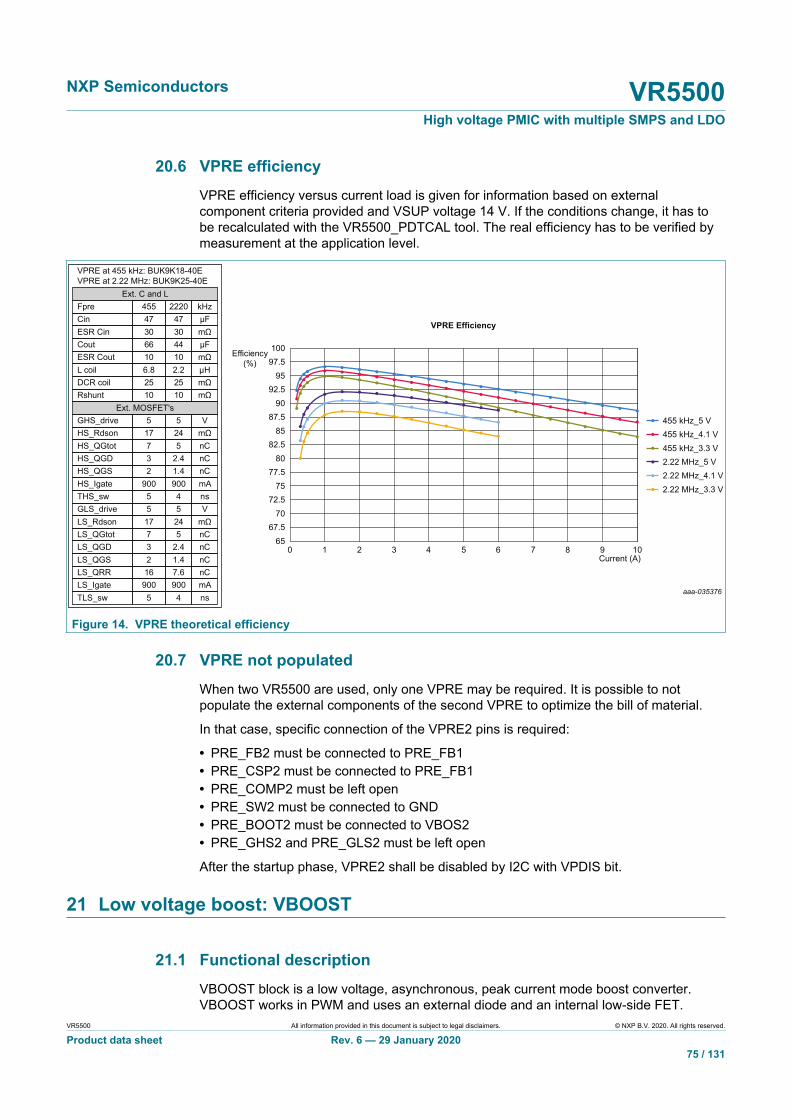
NXP Semiconductors VR5500High voltage PMIC with multiple SMPS and LDO
VR5500 All information provided in this document is subject to legal disclaimers. © NXP B.V. 2020. All rights reserved.
Product data sheet Rev. 6 — 29 January 202075 / 131
20.6 VPRE efficiencyVPRE efficiency versus current load is given for information based on externalcomponent criteria provided and VSUP voltage 14 V. If the conditions change, it has tobe recalculated with the VR5500_PDTCAL tool. The real efficiency has to be verified bymeasurement at the application level.
Current (A)0 1 3 5 7
VPRE Efficiency
98 10642
aaa-035376
Efficiency(%)
65
455 kHz_5 V455 kHz_4.1 V455 kHz_3.3 V2.22 MHz_5 V2.22 MHz_4.1 V2.22 MHz_3.3 V
FpreExt. C and L
Ext. MOSFET's
455 2220Cin 47 47ESR Cin
VPRE at 455 kHz: BUK9K18-40EVPRE at 2.22 MHz: BUK9K25-40E
30 30Cout 66 44ESR Cout 10 10L coil 6.8 2.2
GHS_drive 5 5HS_Rdson 17 24HS_QGtot 7 5HS_QGD 3 2.4HS_QGS 2 1.4HS_Igate 900 900THS_sw 5 4GLS_drive 5 5LS_Rdson 17 24LS_QGtot 7 5LS_QGD 3 2.4LS_QGS 2 1.4
LS_Igate 900 900TLS_sw 5 4
kHzµFmΩµFmΩµH
DCR coil 25 25Rshunt 10 10
mΩmΩ
VmΩnCnCnCmAnsV
mΩnCnCnC
mALS_QRR 16 7.6 nC
ns
67.570
72.575
77.580
82.585
87.590
92.595
97.5100
Figure 14. VPRE theoretical efficiency
20.7 VPRE not populatedWhen two VR5500 are used, only one VPRE may be required. It is possible to notpopulate the external components of the second VPRE to optimize the bill of material.
In that case, specific connection of the VPRE2 pins is required:
• PRE_FB2 must be connected to PRE_FB1• PRE_CSP2 must be connected to PRE_FB1• PRE_COMP2 must be left open• PRE_SW2 must be connected to GND• PRE_BOOT2 must be connected to VBOS2• PRE_GHS2 and PRE_GLS2 must be left open
After the startup phase, VPRE2 shall be disabled by I2C with VPDIS bit.
21 Low voltage boost: VBOOST
21.1 Functional descriptionVBOOST block is a low voltage, asynchronous, peak current mode boost converter.VBOOST works in PWM and uses an external diode and an internal low-side FET.

NXP Semiconductors VR5500High voltage PMIC with multiple SMPS and LDO
VR5500 All information provided in this document is subject to legal disclaimers. © NXP B.V. 2020. All rights reserved.
Product data sheet Rev. 6 — 29 January 202076 / 131
VBOOST enters Skip mode to maintain the correct output voltage in light load condition.The output voltage is configurable by OTP at 5.0 V or 5.74 V, the switching frequencyis 2.22 MHz and the output current is limited to 1.5 A peak input current. The input ofthe boost is connected to the output of VPRE. This block is intended to supply LDO1,LDO2, BUCK3, or an external regulator. The stability is ensured by an internal Type 2compensation network with slope compensation.
By default, VBOOST switching frequency is derived from the internal oscillator, and canbe synchronized with an external frequency signal applied on FIN input pin. The changefrom internal oscillator to external clock or vice versa is controlled by I2C.
An overcurrent detection and a thermal shutdown are implemented to protect the internalMOSFET. If an overcurrent is detected after the LS minimum TON time, the LS is turnedOFF and will be turned ON again at the next rising edge of the switching clock. Theovercurrent induces a duty cycle reduction that could lead to the output voltage graduallydropping, causing an undervoltage condition on one of the cascaded regulators.
Since the current limitation is on the input current, Table 69 summarizes the expectedoutput current capability depending on VPRE and VBOOST voltage configurations and L= 4.7 μH.
Table 69. Output current capabilityVPRE VBOOST IBOOST_OUT
5.0 V 800 mA3.3 V
5.74 V 700 mA
5.0 V 1 A4.1 V
5.74 V 900 mA
5.0 V 5.74 V 1.1 A
An overvoltage protection is implemented on BOOST_LS pin. When VBOOST_OV isdetected during two consecutive turn ON cycles, VBOOST is disabled. An I2C commandis required to enable it again.

NXP Semiconductors VR5500High voltage PMIC with multiple SMPS and LDO
VR5500 All information provided in this document is subject to legal disclaimers. © NXP B.V. 2020. All rights reserved.
Product data sheet Rev. 6 — 29 January 202077 / 131
21.2 Application schematic
aaa-030994
PWM
driver
EPAD
RCOMP
CCOMP
CHF
Vref
LBOOST
DBOOST
COUT_BOOST
BOOST_LS
VBOOST
BOOST
VBOOST
VPRE
CONTROLLER
SLOPECOMPENSATION
gm
Figure 15. BOOST schematic
It is recommended to select a Schottky diode for DBOOST to limit the impact on the SMPSefficiency.
21.3 Compensation network and stabilityThe internal compensation network, made with RCOMP, CCOMP, and CHF is optimized forbest compromise between stability and transient response with RCOMP = 750 kΩ, CCOMP= 125 pF, and CHF = 2.0 pF.
Use case with VBOOST = 5.74 V, LVBOOST = 4.7 μH, FBOOST_SW = 2.22 MHz,COUT_BOOST = 22 μF
Use case stability verification
• Phase margin target PM > 45° and gain margin target GM > 6 dB.
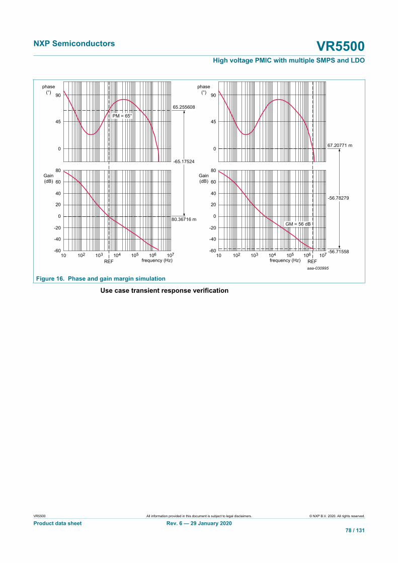
NXP Semiconductors VR5500High voltage PMIC with multiple SMPS and LDO
VR5500 All information provided in this document is subject to legal disclaimers. © NXP B.V. 2020. All rights reserved.
Product data sheet Rev. 6 — 29 January 202078 / 131
aaa-030995
phase(°)
0
-20
20
-40
40
80
60Gain(dB)
-60
-65.17524
65.255608
80.36716 m
-56.78279
67.20771 m
-56.71558
frequency (Hz)10 107104 105 106102 103
REF REF
45
90
0
phase(°)
frequency (Hz)10 107104 105 106102 103
45
90
0
0
-20
20
-40
-60
40
80
60Gain(dB)
PM = 65°
GM = 56 dB
Figure 16. Phase and gain margin simulation
Use case transient response verification

NXP Semiconductors VR5500High voltage PMIC with multiple SMPS and LDO
VR5500 All information provided in this document is subject to legal disclaimers. © NXP B.V. 2020. All rights reserved.
Product data sheet Rev. 6 — 29 January 202079 / 131
aaa-030996
5.6
5.2
5.4
5.8
6.0
6.2VOUT
(V)
5.0
time (ms) 500 µs / div1.0 5.54.52.5 3.51.5 2.0 3.0 4.0 5.0
0
100
200
300
I_OUT(A)
-100
load step from 10 mA to 0.21 A20 mA/µs
2.053190 ms 3.572365 ms1.519175 ms
REF A
min UV - 170 mV
max OV + 150 mV
319.8099 mV
5.891551
5.571741
Figure 17. Transient response simulation
21.4 VBOOST electrical characteristics
Table 70. VBOOST electrical characteristicsTA = −40 °C to 125 °C, unless otherwise specified. VSUP = VSUP_UVH to 36 V, unless otherwise specified. All voltagesreferenced to ground.
Symbol Parameter Min Typ Max Unit
5.57 5.74 5.91 VVBOOST Output voltage (OTP_VBSTV[3:0] bits)
4.85 5.0 5.15 V
Output voltage from 10 % to 90 % — 500 — μsVBOOST_SOFT_START
Digital DAC soft start completion — — 825 µs
VBOOST_STARTUP Overshoot at startup — — 3 %
VBOOST_UVH Undervoltage threshold high 3.3 — 3.7 V
TBOOST_UVH VBOOST_UVH filtering time 6.0 10 15 μs
VBOOST_OV Overvoltage protection threshold 7.4 — 7.9 V
FBOOST_SW Switching frequency range 2.1 2.22 2.35 MHz

NXP Semiconductors VR5500High voltage PMIC with multiple SMPS and LDO
VR5500 All information provided in this document is subject to legal disclaimers. © NXP B.V. 2020. All rights reserved.
Product data sheet Rev. 6 — 29 January 202080 / 131
Symbol Parameter Min Typ Max Unit
LBOOST Inductor for VBOOST_SW = 2.22 MHz 2.2 4.7 6.8 μH
COUT_BOOST Effective output capacitor 22 — 66 μF
VBOOST_LOAD_REG Transient load regulation (COUT_BOOST = 22 μF,from 10 mA to 400 mA, di/dt = 200 mA/μs)
— — 750 mV
VBOOST_LOAD_REG Transient load regulation (COUT_BOOST = 22 μF,from 1.0 mA to 20 mA, di/dt = 200 mA/μs)
— — 500 mV
ILIM_BOOST Inductor peak current limitation range (OTP_VBSTILIM[1:0] bits)
1.5 2.0 2.75 A
40 60 90 nsTBOOST_ON_MIN LS minimum ON time (OTP_VBSTTONTIME[1:0]bits)
30 50 80 ns
RBOOST_RON LS NMOS RDSon — 150 280 mΩ
— 500 1500 V/μsTBOOST_SR Switching output slew rate (OTP_VBSTSR[1:0]bits by default + VBSTSR[1:0] bits by I2C)
— 300 750 V/μs
gmEABOOST Error amplifier transconductance 3.5 7.0 9.0 μS
40 79 110 mV/μs
70 125 190 mV/μs
VBOOST_SLOPE Slope compensation (OTP_VBSTSC[3:0] bits)
90 160 230 mV/μs
500 750 1200 kΩRCOMP Compensation network resistor
250 500 1000 kΩ
CCOMP Compensation network capacitor 90 125 175 pF
TSDBOOST Thermal shutdown threshold 160 — — °C
TSDBOOST_HYST Thermal shutdown threshold hysteresis — 9 — °C
TBOOST_TSD Thermal shutdown filtering time 3.0 5.0 8.0 μs
21.5 VBOOST not populatedIt is possible to not use the VBOOST when VPRE is configured at 4.1 V or 5.0 V. Inthis case, the external VBOOST components can be unpopulated to optimize the bill ofmaterial. The OTP_BOOSTEN bit shall be programmed to 0 and VBOOST pin must beconnected to VPRE. BOOST_LS pin must be left open.
VBOOST must be used when VPRE is configured at 3.3 V or 3.8 V to supply VBOS.
22 Low voltage buck: BUCK1 and BUCK2
22.1 Functional descriptionBUCK1 and BUCK2 blocks are low voltage, synchronous, valley current mode buckconverters with integrated HS PMOS and LS NMOS. BUCK1 and BUCK2 work in forcePWM and the output voltage is configurable by OTP from 0.8 V to 1.8 V, the switchingfrequency is 2.22 MHz and the output current is limited to 3.6 A peak. The input of theseblocks must be connected to the output of VPRE. The stability is ensured by an internalType 2 compensation network with slope compensation.
By default, BUCK1 and BUCK2 switching frequency is derived from the internal oscillatorand can be synchronized with an external frequency signal applied on FIN input pin. Thechange from internal oscillator to external clock or vice versa is controlled by I2C.

NXP Semiconductors VR5500High voltage PMIC with multiple SMPS and LDO
VR5500 All information provided in this document is subject to legal disclaimers. © NXP B.V. 2020. All rights reserved.
Product data sheet Rev. 6 — 29 January 202081 / 131
BUCK1 and BUCK2 can work independently or in Dual phase mode to double the outputcurrent capability. When BUCK1 and BUCK2 are used in dual phase, they must have thesame output voltage configuration. Any action like TSD, OV, disable by I2C, on BUCK1affects BUCK2 and vice versa.
An overcurrent detection and a thermal shutdown are implemented on BUCK1 andBUCK2 to protect the internal MOSFETs. The overcurrent induces a duty cycle reductionthat could lead to the output voltage gradually dropping, causing an undervoltagecondition.
The ramp up and ramp down of BUCK1 and BUCK2 when they are enabled and disabledis configurable with OTP_DVS_BUCK12[1:0] bits to accommodate multiple MCU softstart requirements. Static Voltage Scaling (SVS) feature is available to decrease theoutput voltage after power up during INIT_FS Programmable phase shift control isimplemented, see Section 25 "Clock management".
22.2 Application schematic: Single phase modeIn this configuration, BUCK1 and BUCK2 are configured as independent outputs, workingindependently. Each output is configured and controlled independently by I2C.
INTERNALCOMPENSATION
aaa-030997
DRIVER BUCK1/2_SW
BUCK1/2_FB
EPAD
BUCK1/2_IN
COUT_BUCK1/2
CIN_BUCK1/2
LBUCK1/2
VPRE
VBUCK1/2CONTROLLER
BUCK1/2
Figure 18. BUCK1/2 standalone schematic
22.3 Application schematic: Dual phase modeIn this configuration, BUCK1 and BUCK2 are configured in dual phase mode to doublethe output current capability. The dual phase mode is enable with OTP_VB12MULTIPHbit. The PCB layout of BUCK1 phase and BUCK2 must be symmetric for optimum EMCperformance.
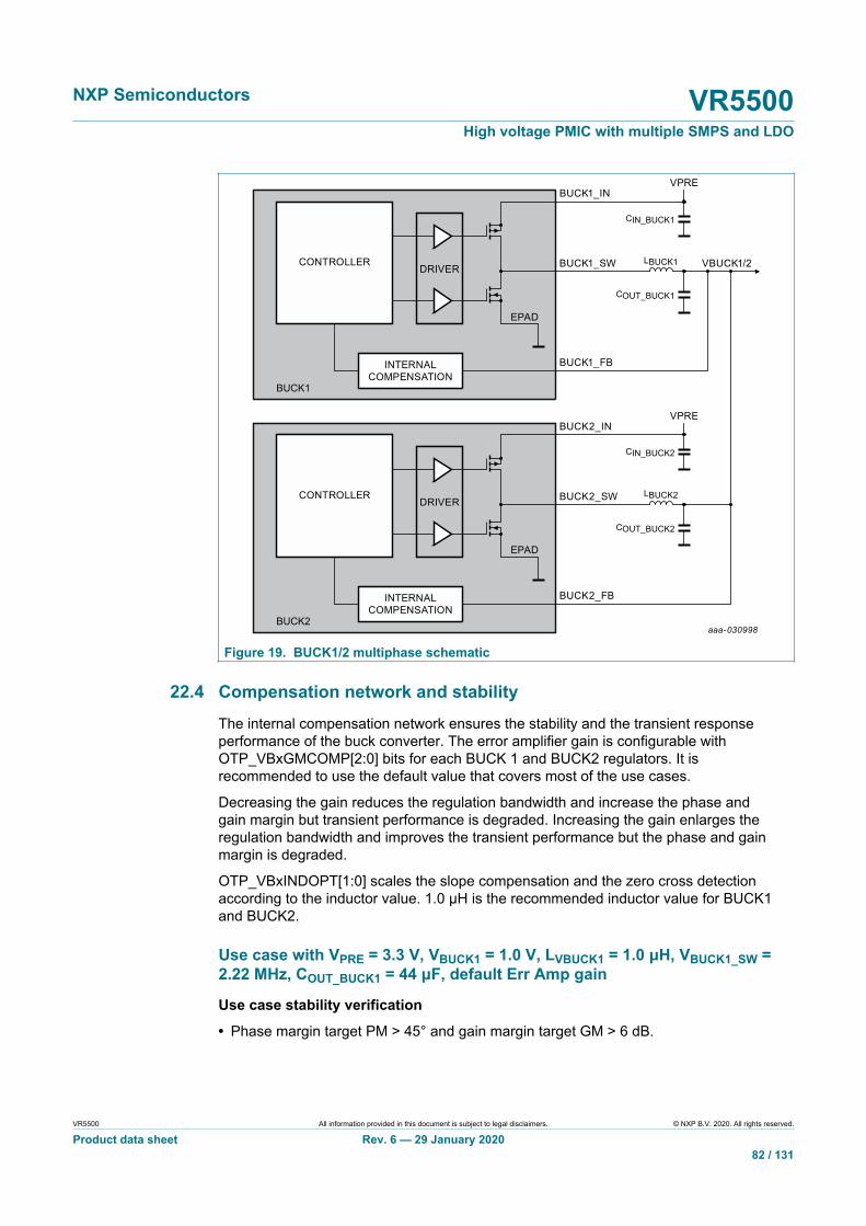
NXP Semiconductors VR5500High voltage PMIC with multiple SMPS and LDO
VR5500 All information provided in this document is subject to legal disclaimers. © NXP B.V. 2020. All rights reserved.
Product data sheet Rev. 6 — 29 January 202082 / 131
INTERNALCOMPENSATION
DRIVER BUCK1_SW
BUCK1_FB
EPAD
BUCK1_IN
COUT_BUCK1
CIN_BUCK1
LBUCK1
VPRE
VBUCK1/2CONTROLLER
BUCK1
INTERNALCOMPENSATION
aaa-030998
DRIVER BUCK2_SW
BUCK2_FB
EPAD
BUCK2_IN
COUT_BUCK2
CIN_BUCK2
LBUCK2
VPRE
CONTROLLER
BUCK2
Figure 19. BUCK1/2 multiphase schematic
22.4 Compensation network and stabilityThe internal compensation network ensures the stability and the transient responseperformance of the buck converter. The error amplifier gain is configurable withOTP_VBxGMCOMP[2:0] bits for each BUCK 1 and BUCK2 regulators. It isrecommended to use the default value that covers most of the use cases.
Decreasing the gain reduces the regulation bandwidth and increase the phase andgain margin but transient performance is degraded. Increasing the gain enlarges theregulation bandwidth and improves the transient performance but the phase and gainmargin is degraded.
OTP_VBxINDOPT[1:0] scales the slope compensation and the zero cross detectionaccording to the inductor value. 1.0 μH is the recommended inductor value for BUCK1and BUCK2.
Use case with VPRE = 3.3 V, VBUCK1 = 1.0 V, LVBUCK1 = 1.0 μH, VBUCK1_SW =2.22 MHz, COUT_BUCK1 = 44 μF, default Err Amp gain
Use case stability verification
• Phase margin target PM > 45° and gain margin target GM > 6 dB.
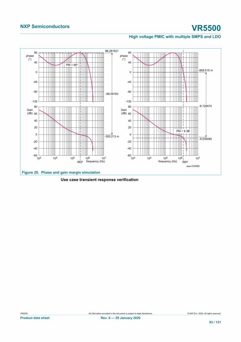
NXP Semiconductors VR5500High voltage PMIC with multiple SMPS and LDO
VR5500 All information provided in this document is subject to legal disclaimers. © NXP B.V. 2020. All rights reserved.
Product data sheet Rev. 6 — 29 January 202083 / 131
aaa-030999
-45
0
-90
45
90phase
(°)
-135
frequency (Hz)103 107106104 105
REF
0
-20
20
-40
40
80
60Gain(dB)
-60
-88.58183
88.281621
-300.213 m
PM = 88°
-45
0
-90
45
90phase
(°)
-135
frequency (Hz)103 107106104 105
REF
0
-20
20
-40
40
80
60Gain(dB)
-60
-8.726570
-808.515 m
-9.535085
PM = 9 dB
Figure 20. Phase and gain margin simulation
Use case transient response verification
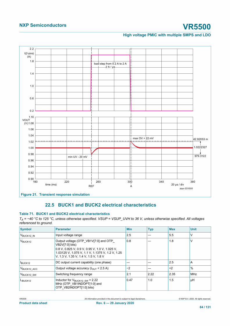
NXP Semiconductors VR5500High voltage PMIC with multiple SMPS and LDO
VR5500 All information provided in this document is subject to legal disclaimers. © NXP B.V. 2020. All rights reserved.
Product data sheet Rev. 6 — 29 January 202084 / 131
aaa-031000
0.98
0.96
1.02
1.00
0.94
0.92
1.06
1.08
1.04
1.10VOUT
(V)
0.90
time (ms) 20 µs / div180 380340260 300220
1.0
1.4
0.6
1.8
2.2I(2-pos)
(A)
0.2
load step from 0.2 A to 2 A2 A / µs
REF A
min UV - 20 mV
max OV + 22 mV
1.0222327
42.92053 m
979.3122
Figure 21. Transient response simulation
22.5 BUCK1 and BUCK2 electrical characteristics
Table 71. BUCK1 and BUCK2 electrical characteristicsTA = −40 °C to 125 °C, unless otherwise specified. VSUP = VSUP_UVH to 36 V, unless otherwise specified. All voltagesreferenced to ground.
Symbol Parameter Min Typ Max Unit
VBUCK12_IN Input voltage range 2.5 — 5.5 V
VBUCK12 Output voltage (OTP_VB1V[7:0] and OTP_VB2V[7:0] bits)0.8 V, 0.825 V, 0.9 V, 0.95 V, 1.0 V, 1.025 V,1.03125 V, 1.075 V, 1.1 V, 1.1375 V, 1.2 V, 1.25V, 1.3 V, 1.35 V, 1.4 V, 1.5 V, 1.8 V
0.8 — 1.8 V
IBUCK12 DC output current capability (one phase) — — 2.5 A
VBUCK12_ACC Output voltage accuracy (IOUT < 2.5 A) −2 — +2 %
VBUCK12_SW Switching frequency range 2.1 2.22 2.35 MHz
LBUCK12 Inductor for VBUCK12_SW = 2.22MHz (OTP_VB1INDOPT[1:0] andOTP_VB2INDOPT[1:0] bits)
0.47 1.0 1.5 μH

NXP Semiconductors VR5500High voltage PMIC with multiple SMPS and LDO
VR5500 All information provided in this document is subject to legal disclaimers. © NXP B.V. 2020. All rights reserved.
Product data sheet Rev. 6 — 29 January 202085 / 131
Symbol Parameter Min Typ Max Unit
Effective Output capacitor 40 — 160 μFCOUT_BUCK12
Output decoupling capacitor — 0.1 — μF
Effective Input capacitor (close to BUCK1_IN andBUCK2_IN pins)
4.7 — — μFCIN_BUCK12
Input decoupling capacitor (close to BUCK1_INand BUCK2_IN pins)
— 0.1 — μF
VBUCK12_TLR Transient load regulation for VBUCK12 < 1.2 V(Cout = 40 μF, from 200 mA to 1.0 A, di/dt = 2.0A/μs), single phase(Cout = 40 μF, from 400 mA to 2.0 A, di/dt = 4.0A/μs), dual phase
−25 — +25 mV
VBUCK12_TLR Transient load regulation for VBUCK12 >1.2 V(Cout = 40 μF, from 200 mA to 1.0 A, di/dt = 2.0A/μs), single phase(Cout = 40 μF, from 400 mA to 2.0 A, di/dt = 4.0A/μs), dual phase
−3 — +3 %
ILIM_BUCK12 Inductor peak current limitation range for onephase (OTP_VB1SWILIM[1:0] and OTP_VB2SWILIM[1:0] bits)
3.6 4.5 5.45 A
Ramp up speed, OTP_DVS_BUCK12[1:0] = 00 5.86 7.81 9.77 mV/μs
Ramp up speed, OTP_DVS_BUCK12[1:0] = 01 2.34 3.13 3.91 mV/μs
Ramp up speed, OTP_DVS_BUCK12[1:0] = 10 1.95 2.60 3.26 mV/μs
VBUCK12_DVS_UP(for VBUCK12 up to 1.5V)
Ramp up speed, OTP_DVS_BUCK12[1:0] = 11 1.67 2.23 2.79 mV/μs
Ramp up speed, OTP_DVS_BUCK12[1:0] = 00 7.33 9.763 12.21 mV/μs
Ramp up speed, OTP_DVS_BUCK12[1:0] = 01 2.93 3.91 4.89 mV/μs
Ramp up speed, OTP_DVS_BUCK12[1:0] = 10 2.44 3.25 4.08 mV/μs
VBUCK12_DVS_UP(for VBUCK12 = 1.8 V)
Ramp up speed, OTP_DVS_BUCK12[1:0] = 11 2.09 2.79 3.49 mV/μs
Ramp down speed, OTP_DVS_BUCK12[1:0] = 00 3.91 5.21 6.51 mV/μs
Ramp down speed, OTP_DVS_BUCK12[1:0] = 01 2.34 3.13 3.91 mV/μs
Ramp down speed, OTP_DVS_BUCK12[1:0] = 10 1.95 2.6 3.26 mV/μs
VBUCK12_DVS_DOWN(for VBUCK12 up to 1.5V)
Ramp down speed, OTP_DVS_BUCK12[1:0] = 11 1.67 2.23 2.79 mV/μs
Ramp down speed, OTP_DVS_BUCK12[1:0] = 00 4.89 6.51 8.14 mV/μs
Ramp down speed, OTP_DVS_BUCK12[1:0] = 01 2.93 3.91 4.89 mV/μs
Ramp down speed, OTP_DVS_BUCK12[1:0] = 10 2.44 3.25 4.08 mV/μs
VBUCK12_DVS_DOWN(for VBUCK12 = 1.8 V)
Ramp down speed, OTP_DVS_BUCK12[1:0] = 11 2.09 2.79 3.49 mV/μs
VBUCK12_SOFT_START = VBUCK12 / VBUCK12_DVS_UPSoft start for VBUCK12 = 1.2 V andOTP_DVS_BUCK12[1:0] = 00
122.9 153.6 204.8 μsTBUCK12_SOFT_START
Soft start for VBUCK12 = 1.2 V andOTP_DVS_BUCK12[1:0] = 11To be recalculated for different VBUCK12 anddifferent VBUCK12_DVS_UP
430.1 538.1 718.5 μs
VBUCK12_STARTUP Overshoot at startup — — 50 mV
TBUCK12_OFF_MIN HS minimum OFF time 9 30 54 ns
TBUCK12_DT Dead time to avoid cross conduction 0.01 3 20 ns
RBUCK12_HS_RON HS PMOS RDSon — — 135 mΩ

NXP Semiconductors VR5500High voltage PMIC with multiple SMPS and LDO
VR5500 All information provided in this document is subject to legal disclaimers. © NXP B.V. 2020. All rights reserved.
Product data sheet Rev. 6 — 29 January 202086 / 131
Symbol Parameter Min Typ Max Unit
RBUCK12_LS_RON LS NMOS RDSon — — 80 mΩ
RBUCK12_DISch Discharge resistance (when BUCK1,2 is disabled) 250 500 1000 Ω
TSDBUCK12 Thermal shutdown threshold 160 — — °C
TSDBUCK12_HYST Thermal shutdown threshold hysteresis — 9 — °C
TBUCK12_TSD Thermal shutdown filtering time 3 5 8 μs
22.6 BUCK1 and BUCK2 efficiencyBUCK1 and BUCK2 efficiency versus current load is given for information based onexternal component criteria provided and VPRE voltage 4.1 V. If the conditions change,it has to be recalculated with the VR5500_PDTCAL tool. The real efficiency has to beverified by measurement at the application level.
Current (A)
BUCK1 Efficiency (VPRE = 4.1 V)
aaa-035374
Efficiency(%)
0.8 V_Eff1.25 V_Eff1.8 V_Eff
CinExt. C and L
Int. MOSFET's
60 µFESR Cin 10 mΩCout 44 µFESR Cout 10 mΩL coil 1 µHDCR coil 20 mΩ
HS_Rdson 135 mΩ
QLS 0.5 nC
QHS 0.5 nCTHS_sw 3 ns
GLS_drive 5 V
GHS_drive 5 VLS_Rdson 80 mΩ
TLS_sw 3 ns
0 2.52.01.0 1.50.5 2.251.750.75 1.250.25
90
85
95
100
80
Figure 22. BUCK1 and BUCK2 theoretical efficiency
23 Low voltage buck: BUCK3
23.1 Functional descriptionBUCK3 block is a low voltage, synchronous, peak current mode buck converter withintegrated HS PMOS and LS NMOS. BUCK3 works in force PWM and the output voltageis configurable by OTP from 1.0 V to 3.3 V, the switching frequency is 2.22 MHz and theoutput current is limited to 3.6 A peak. The input of this block can be connected to theoutput of VPRE or VBOOST when VBOOST = 5.0 V only. The stability is ensured by aninternal Type 2 compensation network with slope compensation.
By default, BUCK3 switching frequency is derived from the internal oscillator, and canbe synchronized with an external frequency signal applied on FIN input pin. The changefrom internal oscillator to external clock or vice versa is controlled by I2C.
An overcurrent detection and a thermal shutdown are implemented on BUCK3 to protectthe internal MOSFETs. The overcurrent induces a duty cycle reduction that could lead tothe output voltage gradually dropping, causing an undervoltage condition.

NXP Semiconductors VR5500High voltage PMIC with multiple SMPS and LDO
VR5500 All information provided in this document is subject to legal disclaimers. © NXP B.V. 2020. All rights reserved.
Product data sheet Rev. 6 — 29 January 202087 / 131
BUCK3 is part number dependent according to OTP_BUCK3EN bit. BUCK3_INQ pin,used to bias internal BUCK3 driver, and must be connected to the same source pin thanBUCK3_IN pin. The ramp up and ramp down of BUCK3 when it is enabled and disabledis configurable with OTP_DVS_BUCK3[1:0] bits to accommodate multiple MCU soft startrequirements.
Programmable phase shift control is implemented, see Section 25 "Clock management".
23.2 Application schematic
INTERNALCOMPENSATION
aaa-031002
DRIVER BUCK3_SW
BUCK3_FB
EPAD
BUCK3_IN
BUCK3_INQ
COUT_BUCK3
CIN_BUCK3
LBUCK3
VPRE or VBOOST
VBUCK3CONTROLLER
BUCK3
Figure 23. BUCK3 schematic
23.3 Compensation network and stabilityThe internal compensation network ensures the stability and the transient responseperformance of the buck converter. OTP_VB3INDOPT[1:0] scales the slopecompensation and the zero cross detection according to inductor value. 1.0 μH is therecommended inductor value for BUCK3.
Use case with VPRE = 3.3 V, VBUCK3 = 2.3 V, LVBUCK3 = 1.0 μH, FBUCK3_SW =2.22 MHz, COUT_BUCK3 = 44 μF
Use case stability verification
• Phase margin target PM > 45° and gain margin target GM > 6 dB.

NXP Semiconductors VR5500High voltage PMIC with multiple SMPS and LDO
VR5500 All information provided in this document is subject to legal disclaimers. © NXP B.V. 2020. All rights reserved.
Product data sheet Rev. 6 — 29 January 202088 / 131
aaa-031003
0
45
-45
90
135phase
(°)
-90
frequency (Hz)103 107106104 105
REF
-20
-40
0
-60
20
60
40Gain(dB)
-80
-65.72816
65.577201
-150.958 m
PM = 65°
0
45
-45
90
135phase
(°)
-90
frequency (Hz)103 107106104 105
REF
-20
-40
0
-60
20
60
40Gain(dB)
-80
-26.56473
-541.098 m
-27.10583
PM = 26 dB
Figure 24. Phase and gain margin simulation
Use case transient response verification

NXP Semiconductors VR5500High voltage PMIC with multiple SMPS and LDO
VR5500 All information provided in this document is subject to legal disclaimers. © NXP B.V. 2020. All rights reserved.
Product data sheet Rev. 6 — 29 January 202089 / 131
aaa-031004
2.40
2.28
2.32
2.24
2.36
2.40VOUT
(V)
2.20
time (ms) 200 µs / div0 1.00.80.4 0.60.2
0.6
0.8
0.4
1.0
1.2I(R9-P)
(A)
0.2
load step from 0.2 A to 1 A2 A / µs
REF A
min UV - 20 mV
max OV + 22 mV
48.22034 mV
2.3219836
2.2737633
Figure 25. Transient response simulation
23.4 BUCK3 electrical characteristics
Table 72. BUCK3 electrical characteristicsTA = −40 °C to 125 °C, unless otherwise specified. VSUP = VSUP_UVH to 36 V, unless otherwise specified. All voltagesreferenced to ground.
Symbol Parameter Min Typ Max Unit
VBUCK3_IN Input voltage range 2.5 — 5.5 V
VBUCK3 Output voltage (OTP_VB3V[4:0] bits)1.0 V, 1.1 V, 1.2 V, 1.25 V, 1.3 V, 1.35 V,1.5 V, 1.6 V, 1.8 V, 2.3 V, 2.5 V, 2.8 V, 3.3 V
1.0 — 3.3 V
IBUCK3 DC output current capability — 2.5 — A
VBUCK3_ACC Output voltage accuracy (Iout < 2.5 A) −2 — +2 %
VBUCK3_SW Switching frequency range 2.1 2.22 2.35 MHz
LBUCK3 Inductor for VBUCK3_SW = 2.22 MHz(OTP_VB3INDOPT[1:0] bits)
0.47 1.0 1.5 μH
Effective output capacitor 40 — 120 μFCOUT_BUCK3
Output decoupling capacitor — 0.1 — μF

NXP Semiconductors VR5500High voltage PMIC with multiple SMPS and LDO
VR5500 All information provided in this document is subject to legal disclaimers. © NXP B.V. 2020. All rights reserved.
Product data sheet Rev. 6 — 29 January 202090 / 131
Symbol Parameter Min Typ Max Unit
Effective input capacitor (close to BUCK3_IN pin) 4.7 — — μFCIN_BUCK3
Input decoupling capacitor (close to BUCK3_INpin)
— 0.1 — μF
VBUCK3_TLR Transient load regulation (Cout = 40 μF, from 200mA to 1.0 A, di/dt = 2.0 A/μs)
−50 — +50 mV
2.0 2.6 3.1 AILIM_BUCK3 Inductor peak current limitation range (OTP_VB3SWILIM[1:0] bits)
3.6 4.5 5.45 A
TBUCK3_ON_MIN HS minimum ON time 5 50 80 ns
Ramp up and ramp down speed, OTP_DVS_BUCK3[1:0] = 00
7.81 10.42 13.02 mV/µs
Ramp up and ramp down speed, OTP_DVS_BUCK3[1:0] = 01
2.6 3.47 4.34 mV/µs
Ramp up and ramp down speed, OTP_DVS_BUCK3[1:0] = 10
1.95 2.6 3.26 mV/µs
VBUCK3_DVS_UP_DOWN
Ramp up and ramp down speed, OTP_DVS_BUCK3[1:0] = 11
1.56 2.08 2.60 mV/µs
VBUCK3_SOFT_START = VBUCK3 / VBUCK3_DVS_UPSoft start for VBUCK3 = 1.8 V andOTP_DVS_BUCK3[1:0] = 00
84.8 105.6 140.08 μsTBUCK3_SOFT_START
Soft start for VBUCK3 = 1.8 V andOTP_DVS_BUCK3[1:0] = 11To be recalculated for different VBUCK3 anddifferent VBUCK3_DVS_UP_DOWN
422.4 528 704 μs
VBUCK3_STARTUP Overshoot at startup — — 50 mV
TBUCK3_DT Dead time to avoid cross conduction 0.01 3 20 ns
RBUCK3_HS_RON HS PMOS RDSon — — 135 mΩ
RBUCK3_LS_RON LS NMOS RDSon — — 80 mΩ
RBUCK3_DISCH Discharge resistance (when BUCK3 is disabled) 250 500 1000 Ω
TSDBUCK3 Thermal shutdown threshold 160 — — °C
TSDBUCK3_HYST Thermal shutdown threshold hysteresis — 9 — °C
TBUCK3_TSD Thermal shutdown filtering time 3 5 8 μs
23.5 BUCK3 efficiencyBUCK3 efficiency versus current load is given for information based on externalcomponent criteria provided and VPRE voltage 4.1 V. If the conditions change, it has tobe recalculated with the VR5500_PDTCAL tool. The real efficiency has to be verified bymeasurement at the application level.

NXP Semiconductors VR5500High voltage PMIC with multiple SMPS and LDO
VR5500 All information provided in this document is subject to legal disclaimers. © NXP B.V. 2020. All rights reserved.
Product data sheet Rev. 6 — 29 January 202091 / 131
Current (A)
BUCK3 Efficiency (VPRE = 4.1 V)
aaa-035375
Efficiency(%)
1.25 V_Eff1.8 V_Eff0.8 V_Eff
CinExt. C and L
Int. MOSFET's
60 µFESR Cin 10 mΩCout 44 µFESR Cout 10 mΩL coil 1 µHDCR coil 20 mΩ
HS_Rdson 135 mΩ
QLS 0.5 nC
QHS 0.5 nCTHS_sw 3 ns
GLS_drive 5 V
GHS_drive 5 VLS_Rdson 80 mΩ
TLS_sw 3 ns
0 2.52.01.0 1.50.5 2.251.750.75 1.250.25
90
85
95
100
80
75
65
70
Figure 26. BUCK3 theoretical efficiency
24 Linear voltage regulator: LDO1, LDO2
24.1 Functional descriptionLDO1 and LDO2 blocks are two linear voltage regulators. The output voltage isconfigurable by OTP from 1.1 V to 5.0 V. A minimum voltage drop is required dependingon the output current capability (0.5 V for 150 mA and 1.0 V for 400 mA). The LDOcurrent capability is linear with the voltage drop and can be estimated to I(mA) = 500 xVLDO12_DROP – 100 for intermediate voltage drop between 0.5 V and 1.0 V.
LDO1 input supply is externally connected to VPRE, VBOOST, or another supply. LDO2input supply is internally connected to the output of VBOOST. An overcurrent detectionand a thermal shutdown are implemented on LDO1 and LDO2 to protect the internalpass device.

NXP Semiconductors VR5500High voltage PMIC with multiple SMPS and LDO
VR5500 All information provided in this document is subject to legal disclaimers. © NXP B.V. 2020. All rights reserved.
Product data sheet Rev. 6 — 29 January 202092 / 131
24.2 Application schematics
aaa-032950
I2CINTERFACE
VLDO1_EN
LDO1_IN
VLDO1
CIN_LDO1
COUT_LDO1
VLDO1_IN
discharge
VREF
VLDO1
Figure 27. LDO1 block diagram
aaa-032951
I2CINTERFACE
VLDO2_EN
VLDO2
VBOOST
COUT_LDO2
discharge
VREF
VLDO2
Figure 28. LDO2 block diagram

NXP Semiconductors VR5500High voltage PMIC with multiple SMPS and LDO
VR5500 All information provided in this document is subject to legal disclaimers. © NXP B.V. 2020. All rights reserved.
Product data sheet Rev. 6 — 29 January 202093 / 131
24.3 LDO1 and LDO2 electrical characteristics
Table 73. LDO1 and LDO2 electrical characteristicsTA = −40 °C to 125 °C, unless otherwise specified. VSUP = VSUP_UVH to 36 V, unless otherwise specified. All voltagesreferenced to ground.Symbol Parameter Min Typ Max Unit
VLDO12_IN Input voltage range 2.5 — 6.5 V
VLDO12 Output voltage (OTP_VLDO1V[2:0] and OTP_LDO2V[2:0]bits)1.1 V, 1.2 V, 1.6 V, 1.8 V, 2.5 V, 2.8 V, 3.3 V, 5.0 V
1.1 — 5.0 V
VLDO12_ACC_150 Output voltage accuracy, 150 mA current capability −2 — +2 %
VLDO12_ACC_400 Output voltage accuracy, 400 mA current capability −3 — +3 %
VLDO12_DROP_150 Minimum voltage drop for 150 mA current capability 0.5 — — V
VLDO12_DROP_400 Minimum voltage drop for 400 mA current capability 1.0 — — V
CIN_LDO1 Input capacitor (close to LDO1_IN pin) 1.0 — — μF
COUT_LDO12_150 Output capacitor, 150 mA current capability 4.7 — 10 μF
COUT_LDO12_400 Output capacitor, 400 mA current capability 6.8 — 10 μF
COUT_LDO12 Output decoupling capacitor 0.1 — — μF
VLDO12_LTR_150 Transient load regulation (from 10 mA to 150 mA in 2.0 μs) −4 — +4 %
VLDO12_LTR_400 Transient load regulation (from 10 mA to 400 mA in 4.0 μs) −5 — +5 %
VLDO12_LR Line regulation — — 0.5 %
VLDO12_ILIM_150 Current limitation, 150 mA current capability (OTP_LDO1ILIM and OTP_LDO2ILIM bits)
200 280 500 mA
VLDO12_ILIM_400 Current limitation, 400 mA current capability (OTP_LDO1ILIM and OTP_LDO2ILIM bits)
430 560 800 mA
VLDO12_SOFT_START Soft start (enable to 90 %) — 1.0 1.3 ms
VLDO12_STARTUP Overshoot at startup — — 2 %
RLDO12_DISCH Discharge resistance (when LDO1,2 is disabled) 10 20 60 Ω
TSDLDO12 Thermal shutdown threshold 160 — — °C
TSDLDO12_HYST Thermal shutdown threshold hysteresis — 9 — °C
TLDO12_TSD Thermal shutdown filtering time 3 5 8 μs
25 Clock management
25.1 Clock descriptionThe clock management block is made of the internal oscillator, the Phase Locked Loop(PLL) and multiple dividers. This block manages the clock generation for the internaldigital state machines, the switching regulators, and the external clock synchronization.
The internal oscillator is running at 20 MHz by default after startup. The frequency isprogrammable by I2C and a spread spectrum feature can be activated by I2C to reducethe emission of the oscillator fundamental frequency.
VPRE switching frequency is coming from CLK2 (455 kHz) or CLK1 (2.22 MHz).BUCK1,2,3 and BOOST switching frequency is coming from CLK1 (2.22 MHz). Theswitching regulators can be synchronized with an external frequency coming from FINpin. A dedicated watchdog monitoring is implemented to verify and report the correct FINfrequency range. Different clocks can be sent to FOUT pin to synchronize an external ICor for diagnostic.

NXP Semiconductors VR5500High voltage PMIC with multiple SMPS and LDO
VR5500 All information provided in this document is subject to legal disclaimers. © NXP B.V. 2020. All rights reserved.
Product data sheet Rev. 6 — 29 January 202094 / 131
aaa-031008
20 MHz INT. OSC(SPREAD SPECTRUM,
FREQ TUNING)enable
CLK2
CLK1
PLL x 48
out
in
DIVIDER/48
DIVIDER 2/44 (OTP)
PHASESHIFTING
FOUT_clkVPRE_clk
BUCK1,2,3_clkBOOST_clk
FOUT
PHASESHIFTING0
1FIN
VDDI2C
DIVIDER/1, /6
CLK_FIN_DIVMONITORING
OSC_MAIN/48
CLK_FIN_DIV
EXT_FIN_SELEXT_FIN_DIS
Vddio
FOUT_MUX_SEL
FOUT_clkVPRE_clk
BUCKs & BOOST_clkCLK_FIN_DIVOSC_Main/48
OSC_FS/48
DIVIDER 1/9 (OTP)
0
1OTP:PLL_SEL
Figure 29. Clock management block diagram
25.2 Phase shiftingThe clocks of the switching regulators (VPRE_clk, BOOST_clk, BUCK1_clk, BUCK2_clkand BUCK3_clk) can be delayed in order to avoid all the regulators to turn ON at thesame time to reduce peak current and improve EMC performance.
Each clock of each regulator can be shifted from 1 to 7 clock cycles of CLK runningat 20 MHz what corresponds to 50 ns. The phase shift configuration is done by OTPconfiguration using OTP_VPRE_ph[2:0], OTP_VBST_ph[2:0], OTP_BUCK1_ph[2:0],OTP_BUCK2_ph[2:0], and OTP_BUCK3_ph[2:0].
VPRE and BUCK3 have a peak current detection architecture. The PWM synchronizesthe turn ON of the high-side switch. BUCK1 and BUCK2 have a valley current detectionarchitecture. The PWM synchronizes the turn ON of the low-side switch.
Figure 30. BUCK1,2,3_clk = 2.22 MHz without clock phase shifting

NXP Semiconductors VR5500High voltage PMIC with multiple SMPS and LDO
VR5500 All information provided in this document is subject to legal disclaimers. © NXP B.V. 2020. All rights reserved.
Product data sheet Rev. 6 — 29 January 202095 / 131
Figure 31. BUCK1,2,3_clk = 2.22 MHz with clock phase shifting
25.3 Manual frequency tuningThe internal oscillator frequency, 20 MHz by default, can be programmed from 16 MHzto 24 MHz with 1.0 MHz frequency step by I2C. The oscillator functionality is guaranteedfor frequency increment of one step at a time in either direction, with a minimum of 10μs between two steps. For any unused code of the CLK_TUNE [3:0] bits, the internaloscillator is set at the default 20 MHz frequency.
To change the internal oscillator frequency from 20 MHz to 24 MHz, four I2C commandsare required with 10 μs wait time between each command (21 MHz – wait 10 μs – 22MHz – wait 10 μs – 23 MHz – wait 10 μs – 24 MHz). To change the internal oscillatorfrequency from 24 MHz to 16 MHz, eight I2C commands are required with 10 μs waittime between each command (23 MHz – wait 10 μs – 22 MHz – wait 10 μs – 21 MHz– wait 10 μs – 20 MHz – wait 10 μs – 19 MHz – wait 10 μs – 18 MHz – wait 10 μs – 17MHz – wait 10 μs – 16 MHz).
Table 74. Manual frequency tuning configurationCLK_TUNE [3:0] Oscillator frequency [MHz]
0000 (default) 20
0001 21
0010 22
0011 23
0100 24
1001 16
1010 17
1011 18
1100 19
Reset condition POR
25.4 Spread spectrumThe internal oscillator can be modulated with a triangular carrier frequency of 23 kHz or94 kHz with ±5 % deviation range around the oscillator frequency. The spread spectrumfeature can be activated by I2C with the MOD_EN bit and the carrier frequency can beselected by I2C with the MOD_CONF bit. By default, the spread spectrum is disabled.

NXP Semiconductors VR5500High voltage PMIC with multiple SMPS and LDO
VR5500 All information provided in this document is subject to legal disclaimers. © NXP B.V. 2020. All rights reserved.
Product data sheet Rev. 6 — 29 January 202096 / 131
The spread spectrum and the manual frequency tuning functions cannot be used at thesame time.
The main purpose of the spread spectrum is to improve the EMC performance byspreading the energy of the internal oscillator and VPRE frequency on VBAT frequencyspectrum. It is recommended to select 23 kHz carrier frequency when VPRE isconfigured at 455 kHz and 94 kHz when VPRE is configured at 2.2 MHz for the bestperformance.
25.5 External clock synchronizationTo synchronize the switching regulators with an external frequency coming from FIN pin,the PLL is enabled with OTP_PLL_SEL bit. The FIN pin accepts two ranges of frequencydepending on the divider selection to always have CLK clock at the output of the PLL inthe working range of the digital blocks from 16 MHz to 24 MHz. When FIN_DIV = 0, theinput frequency range must be between 333 kHz and 500 kHz. When FIN_DIV = 1, theinput frequency range must be between 2.0 MHz and 3.0 MHz.
After the FIN clock divider configuration with FIN_DIV bit, the FIN clock is routed to thePLL input with EXT_FIN_SEL bit. The CLK clock changes from the internal oscillator toFIN external clock with EXT_FIN_SEL bit. So, the configuration procedure is FIN_DIVfirst, then apply FIN and finally set EXT_FIN_SEL.
If FIN is out of range, CLK clock moves back to the internal oscillator and reportsthe error using the CLK_FIN_DIV_OK bit. When FIN comes back in the range, theconfiguration procedure described above is executed again.
The FOUT pin can be used to synchronize an external device with the VR5500. Thefrequency sent to FOUT is selected by I2C with the FOUT_MUX_SEL [3:0] bits.
Table 75. FOUT multiplexer selectionFOUT_MUX_SEL [3:0] FOUT multiplexer selection
0000 (default) No signal, FOUT is low
0001 VPRE_clk
0010 BOOST_clk
0011 BUCK1_clk
0100 BUCK2_clk
0101 BUCK3_clk
0110 FOUT_clk (CLK1 or CLK2 selected with FOUT_CLK_SEL bit)
0111 OSC_MAIN/48 (when PLL is enabled by OTP)
1000 OSC_FS/48
1001 CLK_FIN_DIV
Others No signal, FOUT is low
Reset condition POR

NXP Semiconductors VR5500High voltage PMIC with multiple SMPS and LDO
VR5500 All information provided in this document is subject to legal disclaimers. © NXP B.V. 2020. All rights reserved.
Product data sheet Rev. 6 — 29 January 202097 / 131
25.6 Electrical characteristics
Table 76. Electrical characteristicsTA = −40 °C to 125 °C, unless otherwise specified. VSUP = VSUP_UVH to 36 V, unless otherwise specified. All voltagesreferenced to ground.
Symbol Parameter Min Typ Max Unit
20 MHz internal oscillator
F20MHz Oscillator nominal frequency (programmable) — 20 — MHz
F20MHz_ACC Oscillator accuracy −6 — +6 %
T20MHz_step Oscillator frequency tuning step transition time — 10 — μs
Spread spectrum
— 23 — kHzFSSMOD Spread spectrum frequency modulation (MOD_CONF I2C configuration)
— 94 — kHz
FSSRANGE Spread spectrum range (around the nominalfrequency)
−5 — +5 %
Clock synchronization (FIN)
VFIN_IN Input voltage range — VDDI2C — V
DCFIN_FOUT FIN and FOUT duty cycle 40 50 60 %
333 417 500 kHzFINRANGE FIN input frequency range (FIN_DIV I2Cconfiguration)
2.25 2.5 2.75 MHz
FINVIL FIN low-voltage threshold 0.3 x VDDI2C — — V
FINVIH FIN high-voltage threshold — — 0.7 x VDDI2C V
FINHYST FIN hysteresis 0.1 — — V
FINIPD FIN internal pull-down current source 7 10 13 μA
FINDLY FIN input buffer propagation delay — — 8 ns
FINERR_LONG CLK_FIN_DIV monitoring, long deviationdetection
5 — — μs
FINERR_SHORT CLK_FIN_DIV monitoring, short deviationdetection
— — 1.5 μs
FINTLOST Time to switch to internal oscillator when FIN islost
— — 3 μs
Clock synchronization (FOUT)
VFOUT_OUT Output voltage range — VDDIO — V
FOUTVOL FOUT low-voltage threshold at 2.0 mA — — 0.5 V
FOUTVOH FOUT high-voltage threshold at −2.0 mA VDDIO − 0.5 — — V
IFOUT 3-state leakage current (VDDIO = 5.0 V) −1.0 — 1.0 μA
FOUTTRISE FOUT rise time (from 20 % to 80 % of VDDIO,Cout = 30 pF)
— — 20 ns
FOUTTFALL FOUT fall time (from 80 % to 20 % of VDDIO,Cout = 30 pF)
— — 20 ns
PLLTLOCK PLL lock time — — 90 μs
PLLTSET PLL settling time (from EXT_FIN_DIS enable to±1 % of output frequency)
— — 125 μs
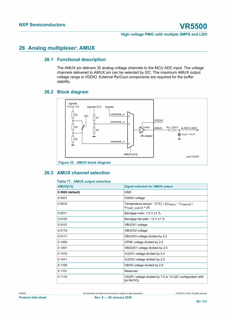
NXP Semiconductors VR5500High voltage PMIC with multiple SMPS and LDO
VR5500 All information provided in this document is subject to legal disclaimers. © NXP B.V. 2020. All rights reserved.
Product data sheet Rev. 6 — 29 January 202098 / 131
26 Analog multiplexer: AMUX
26.1 Functional descriptionThe AMUX pin delivers 32 analog voltage channels to the MCU ADC input. The voltagechannels delivered to AMUX pin can be selected by I2C. The maximum AMUX outputvoltage range is VDDIO. External Rs/Cout components are required for the bufferstability.
26.2 Block diagram
aaa-032952
channels_x
signalssignals /2.5signals
/7.5 or /14
I2C x
z
channels_yx
channels_z
AGND
VDDIO
AMUX to MCU ADC
Cout = 10 nF
Rs = 220 Ωbuffer
AMUX [4:0]
R1
R2R4
R3
R5
Figure 32. AMUX block diagram
26.3 AMUX channel selection
Table 77. AMUX output selectionAMUX[4:0] Signal selection for AMUX output
0 0000 (default) GND
0 0001 VDDIO voltage
0 0010 Temperature sensor : T() = [(VAMUX − VTEMP25) /VTEMP_COEFF] + 25
0 0011 Bandgap main: 1.0 V ±1 %
0 0100 Bandgap fail-safe: 1.0 V ±1 %
0 0101 VBUCK1 voltage
0 0110 VBUCK2 voltage
0 0111 VBUCK3 voltage divided by 2.5
0 1000 VPRE voltage divided by 2.5
0 1001 VBOOST voltage divided by 2.5
0 1010 VLDO1 voltage divided by 2.5
0 1011 VLDO2 voltage divided by 2.5
0 1100 VBOS voltage divided by 2.5
0 1101 Reserved
0 1110 VSUP1 voltage divided by 7.5 or 14 (I2C configuration withbit RATIO)

NXP Semiconductors VR5500High voltage PMIC with multiple SMPS and LDO
VR5500 All information provided in this document is subject to legal disclaimers. © NXP B.V. 2020. All rights reserved.
Product data sheet Rev. 6 — 29 January 202099 / 131
AMUX[4:0] Signal selection for AMUX output
0 1111 WAKE1 voltage divided by 7.45 or 13.85 (I2C configurationwith bit RATIO)
1 0000 WAKE2 voltage divided by 7.45 or 13.85 (I2C configurationwith bit RATIO)
1 0001 Vana: internal main analog voltage supply: 1.6 V ±2 %
1 0010 Vdig: internal main digital voltage supply: 1.6 V ±2 %
1 0011 Vdig_fs: internal fail-safe digital voltage supply: 1.6 V ±2 %
1 0100 PSYNC voltage
Others Same as default value (00000): GND
26.4 AMUX electrical characteristics
Table 78. AMUX electrical characteristicsTA = −40 °C to 125 °C, unless otherwise specified. VSUP = VSUP_UVH to 36 V, unless otherwise specified. All voltagesreferenced to ground.
Symbol Parameter Min Typ Max Unit
VAMUX_VDDIO Minimum VDDIO operating voltage for AMUX 3.2 — — V
VAMUX_IN Input voltage range for VSUP, WAKE1, WAKE2• Ratio 7.45 and 7.5• Ratio 13.85 and 14
2.254.2
——
22.542
V
IAMUX Output buffer current capability — — 2.0 mA
VAMUX_OFF Offset voltage (Iout = 1.0 mA) −7 — +7 mV
VAMUX_RATIO Ratio accuracy• Ratio 1• Ratio 2.5• Ratio 7.5 for VSUP1• Ratio 7.45 for WAKE12• Ratio 14 for VSUP1• Ratio 13.85 for WAKE12
−0.5−1.5−2.0−2.0−2.0−2.0
——————
0.51.52.02.02.02.0
%
VAMUX_BRIDGE VSUP1, WAKE1, WAKE2 resistor bridge 0.75 1.5 3 MΩ
VTEMP25 Temperature sensor voltage at 25 °C 2.01 2.07 2.12 V
VTEMP_COEFF Temperature sensor coefficient −6.25 −6 −5.75 mV/°C
TAMUX_SET Settling time (from 10 % to 90 % of VDDIO, Rs =220 Ω, Cout = 10 nF)
— — 10 μs
Rs Output resistor — 220 — Ω
Cout Output capacitor — 10 — nF
26.5 1.8 V MCU ADC input use caseVR5500 AMUX buffer is referenced to VDDIO, 3.3 V, or 5.0 V. In case the MCU requiresa 1.8 V ADC input voltage, an external resistor bridge R1/R2 can be added in betweenAMUX output and ADC input as shown in Figure 33. It is recommended to use 0.1 %resistor accuracy to limit the conversion error impact.

NXP Semiconductors VR5500High voltage PMIC with multiple SMPS and LDO
VR5500 All information provided in this document is subject to legal disclaimers. © NXP B.V. 2020. All rights reserved.
Product data sheet Rev. 6 — 29 January 2020100 / 131
aaa-031012
AGND
VDDIO (3.3 V or 5.0 V)
AMUX
Optional: for 1.8 V ADC
to MCU ADCRs R1
Cout R2
buffer
Figure 33. Optional 1.8 V ADC use case
The total resistor bridge value (R1 + R2) shall consume between min 10x ADC inputcurrent and max 1 mA at AMUX output to neither disturb the AMUX output buffer nor theADC input. A good estimate is to calculate the resistor bridge value for 200 μA currentconsumption at VDDIO = 3.3 V.
Target R1 + R2 = 20 kΩ
For VDDIO = 3.3 V, R2 / (R1 + R2) = 1.8 / 3.3 = 0.545
After calculation, R2 = 11 kΩ and R1 = 9.3 kΩ
27 I/O interface pins
27.1 WAKE1, WAKE2WAKE pins are used to manage the internal biasing of the device and the main statemachine transitions.
• When WAKE1 or WAKE2 is > WAKE12VIH, the internal biasing is started and theequivalent digital state is '1'
• When WAKE1 or WAKE2 is < WAKE12VIL, the equivalent digital state is '0'• When WAKE1 and WAKE2 are < WAKE12AVIL, the internal biasing is stopped if the
device was in Standby mode
WAKE1 and WAKE2 are level based wake-up input signals with analog measurementcapability through AMUX. WAKE1 can be, for example, connected to a switched VBAT(KL 15 line) and WAKE2 to the wake-up output of a CAN or FlexRay transceiver. Whena WAKE pin is used as a global pin, a C-R-C protection is required (see Section 29"Application information").
Table 79. WAKE1, WAKE2 electrical characteristicsTA = −40 °C to 125 °C, unless otherwise specified. VSUP = VSUP_UVH to 36 V, unless otherwise specified. All voltagesreferenced to ground.
Symbol Parameter Min Typ Max Unit
WAKE12AVIL Analog low input voltage threshold 1.0 — — V
WAKE12VIL Digital low input voltage threshold 2.0 — — V
WAKE12VIH Digital high input voltage threshold — — 4.0 V
Input current leakage at WAKE12 = 36 V — — 100 µAIWAKE12
Input current leakage at WAKE12 = 60 V — — 300 μA
TWAKE12 Filtering time 50 70 100 μs

NXP Semiconductors VR5500High voltage PMIC with multiple SMPS and LDO
VR5500 All information provided in this document is subject to legal disclaimers. © NXP B.V. 2020. All rights reserved.
Product data sheet Rev. 6 — 29 January 2020101 / 131
27.2 INTBINTB is an open drain output pin with internal pull up to VDDIO. This pin generates apulse when an internal interrupt occurs to inform the MCU. Each interrupt can be maskedby setting the corresponding inhibit interrupt bit in M_INT_MASK registers.
Table 80. INTB electrical characteristicsTA = −40 °C to 125 °C, unless otherwise specified. VSUP = VSUP_UVH to 36 V, unless otherwise specified. All voltagesreferenced to ground.
Symbol Parameter Min Typ Max Unit
INTBPULL-up Internal pull-up resistor to VDDIO 5.5 10 15 kΩ
INTBVOL Low output level threshold (I = 2.0 mA) — — 0.5 V
INTBPULSE Pulse duration (without manual frequency tuning) 90 100 110 μs
Table 81. List of interrupts from main logicInterrupt main Description
VSUP_UV7 VSUP undervoltage 7.0 V
VSUP_UVH VSUP undervoltage high
VSUP_UVL VSUP undervoltage low
VBOS_UVH VBOS undervoltage high
VPRE_OC VPRE overcurrent
VPRE_FB_OV VPRE overvoltage protection
VPRE_UVH VPRE undervoltage high
BUCK1_TSD BUCK1 overtemperature shutdown event
BUCK1_OC BUCK1 overcurrent
BUCK2_TSD BUCK2 over temperature shutdown event
BUCK2_OC BUCK2 overcurrent
BUCK3_TSD BUCK3 overtemperature shutdown event
BUCK3_OC BUCK3 overcurrent
BOOST_TSD BOOST overtemperature shutdown event
VBOOST_OV BOOST overvoltage
VBOOST_UVH BOOST undervoltage high
LDO1_TSD LDO1 overtemperature shutdown event
LDO1_OC LDO1 overcurrent
LDO2_TSD LDO2 overtemperature shutdown event
LDO2_OC LDO2 overcurrent
WAKE1 WAKE1 transition
WAKE2 WAKE2 transition
COM I2C communication error

NXP Semiconductors VR5500High voltage PMIC with multiple SMPS and LDO
VR5500 All information provided in this document is subject to legal disclaimers. © NXP B.V. 2020. All rights reserved.
Product data sheet Rev. 6 — 29 January 2020102 / 131
Table 82. List of interrupts from fail-safe logicInterrupt fail-safe Description
VCOREMON_OV VCOREMON overvoltage detected
VCOREMON_UV VCOREMON undervoltage detected
VDDIO_OV VDDIO overvoltage detected
VDDIO_UV VDDIO undervoltage detected
VMON1_OV VMON1 overvoltage detected
VMON1_UV VMON1 undervoltage detected
27.3 PSYNC for two VR5500PSYNC function allows to manage complex startup sequence with multiple powermanagement ICs like two VR5500 (OTP_PSYNC_CFG = 0) or one VR5500 plus onePF82 (OTP_PSYNC_CFG = 1). This function is enabled with the OTP_PSYNC_EN bit.
When PSYNC is used to synchronize two VR5500, PSYNC pins of each device shallbe connected together and pulled up to VBOS pin of the VR5500 master device asshown in Figure 34. In this configuration, VR5500 #1 state machine stops before VR5500#1_VPRE starts and waits for VR5500 #2 to synchronize VR5500#2_VPRE start.
aaa-032955
sync_into digital
VR5500 #1
PSYNC
sync_outfrom digital
VBOS
PSYNCIPD
PSYNCRPU
PSYNCCOUT
sync_into digital
VR5500 #2
PSYNC
sync_outfrom digital
VBOS
PSYNCIPD
Figure 34. Synchronization of two VR5500

NXP Semiconductors VR5500High voltage PMIC with multiple SMPS and LDO
VR5500 All information provided in this document is subject to legal disclaimers. © NXP B.V. 2020. All rights reserved.
Product data sheet Rev. 6 — 29 January 2020103 / 131
aaa-032956
VR5500 #2 ready
VR5500 #1 ready
VSUP
VR5500 #1,Sync_out
VR5500 #1,VPRE
PSYNC
VR5500 #1,Sync_in
VR5500 #2,Sync_out
VR5500 #2,VPRE
VR5500 #2,Sync_in
T
VR5500 ready means VSUP > VSUP_UVH and WAKE1or WAKE2 > WAKE12VIH
During T, VR5500 #1 Sync_in is held low by VR5500 #2Sync_out
Whatever the start up delay T between the 2 x VR5500devices, PSYNC synchronization allows both VPRE tostart at the same time.
Figure 35. Two VR5500 synchronization timing diagram
27.4 PSYNC for VR5500 and external PMICWhen PSYNC is used to synchronize one VR5500 and one external PMIC, PSYNC pinof VR5500 is connected to PGOOD pin of the external PMIC.
When the external PMIC is PF82 from NXP, it can be pulled up to VSNVS pin of PF82.In this configuration, VR5500 state machine stops after VPRE starts and waits for thePGOOD pin of the external PMIC to be released to continue its own power sequencing. Itallows to synchronize the power up sequence of both devices.
During power-down sequence, VR5500 should wait for the external PMIC power-downsequence completion before turning OFF VPRE (VPRE is powering the external PMIC).OTP_VPRE_off_dly bit is configured to extend VPRE turn OFF delay from 250 μs defaultvalue to 32 ms.
aaa-032957
sync_into digital
VR5500
PF82
PSYNC PGOOD
sync_outfrom digital
VSNVS
PSYNCIPD
PSYNCRPU
PSYNCCOUT
LOGIC
Figure 36. Synchronization of one VR5500 and one external PMIC (PF82)

NXP Semiconductors VR5500High voltage PMIC with multiple SMPS and LDO
VR5500 All information provided in this document is subject to legal disclaimers. © NXP B.V. 2020. All rights reserved.
Product data sheet Rev. 6 — 29 January 2020104 / 131
aaa-032958
PF82 PGOOD release
VR5500 VPRE starts
VSUP
PSYNC
VR5500 VREGx
PF82 PGOOD
VR5500 VPRE
PF82 VREGx
VR5500 Sync_in
VR5500 Sync_out
T
When VR5500 VPRE starts, VR5500 waits PSYNCto be released by PF82 PGOOD beforecontinuing its own power up sequence.
Whatever PF82 power up sequence durationT, PSYNC synchronization allows
sequential power up sequencing.
Figure 37. VR5500 and one external PMIC (PF82) synchronization timing diagram
Table 83. PSYNC electrical characteristicsTA = −40 °C to 125 °C, unless otherwise specified. VSUP = VSUP_UVH to 36 V, unless otherwise specified. All voltagesreferenced to ground.
Symbol Parameter Min Typ Max Unit
PSYNCVIL Low-level input voltage threshold 1.0 — — V
PSYNCVIH High-level input voltage threshold — — 2.0 V
PSYNCHYST Hysteresis 0.1 — — V
PSYNCVOL Low-level output threshold (I = 2.0 mA) — — 0.5 V
PSYNCIPD Internal pull down current source 7.0 10 13 μA
PSYNCRPU External pull up resistor to VBOS — 10 — kΩ
PSYNCCOUT External decoupling capacitor — 0.1 — μF
PSYNCTFB Feedback filtering time 6.0 10 15 μs
28 I2C interface
28.1 I2C interface overviewThe VR5500 uses an I2C interface following the high-speed mode definition up to 3.4Mbit/s. I2C interface protocol requires a device address for addressing the target IC on amulti-device bus. The VR5500 has two device address: one to access the main logic andone to access the fail-safe logic. These two I2C addresses are set by OTP.
The I2C interface is using a dedicated power input pin VDDI2C and it is compatible with1.8 V / 3.3 V input supply. Timing, diagrams, and further details can be found in the NXPI2C specification UM10204 rev6.
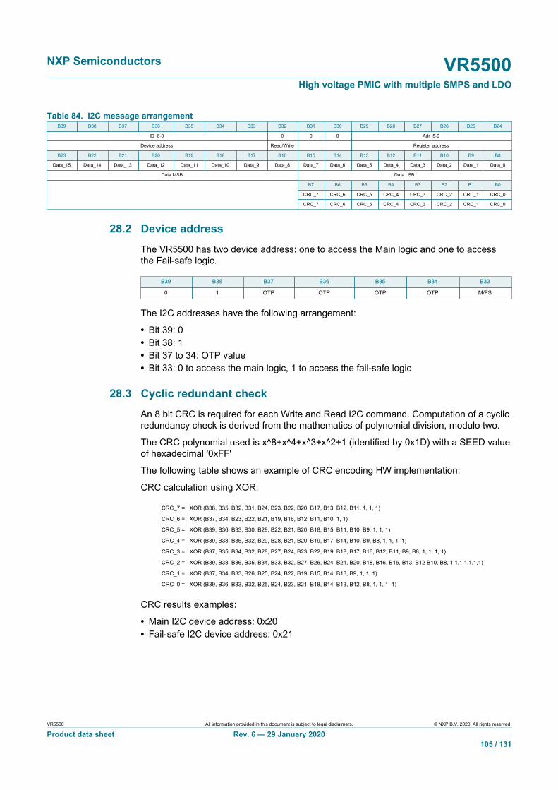
NXP Semiconductors VR5500High voltage PMIC with multiple SMPS and LDO
VR5500 All information provided in this document is subject to legal disclaimers. © NXP B.V. 2020. All rights reserved.
Product data sheet Rev. 6 — 29 January 2020105 / 131
Table 84. I2C message arrangementB39 B38 B37 B36 B35 B34 B33 B32 B31 B30 B29 B28 B27 B26 B25 B24
ID_6-0 0 0 0 Adr_5-0
Device address Read/Write Register address
B23 B22 B21 B20 B19 B18 B17 B16 B15 B14 B13 B12 B11 B10 B9 B8
Data_15 Data_14 Data_13 Data_12 Data_11 Data_10 Data_9 Data_8 Data_7 Data_6 Data_5 Data_4 Data_3 Data_2 Data_1 Data_0
Data MSB Data LSB
B7 B6 B5 B4 B3 B2 B1 B0
CRC_7 CRC_6 CRC_5 CRC_4 CRC_3 CRC_2 CRC_1 CRC_0
CRC_7 CRC_6 CRC_5 CRC_4 CRC_3 CRC_2 CRC_1 CRC_0
28.2 Device addressThe VR5500 has two device address: one to access the Main logic and one to accessthe Fail-safe logic.
B39 B38 B37 B36 B35 B34 B33
0 1 OTP OTP OTP OTP M/FS
The I2C addresses have the following arrangement:
• Bit 39: 0• Bit 38: 1• Bit 37 to 34: OTP value• Bit 33: 0 to access the main logic, 1 to access the fail-safe logic
28.3 Cyclic redundant checkAn 8 bit CRC is required for each Write and Read I2C command. Computation of a cyclicredundancy check is derived from the mathematics of polynomial division, modulo two.
The CRC polynomial used is x^8+x^4+x^3+x^2+1 (identified by 0x1D) with a SEED valueof hexadecimal '0xFF'
The following table shows an example of CRC encoding HW implementation:
CRC calculation using XOR:
CRC_7 = XOR (B38, B35, B32, B31, B24, B23, B22, B20, B17, B13, B12, B11, 1, 1, 1)
CRC_6 = XOR (B37, B34, B23, B22, B21, B19, B16, B12, B11, B10, 1, 1)
CRC_5 = XOR (B39, B36, B33, B30, B29, B22, B21, B20, B18, B15, B11, B10, B9, 1, 1, 1)
CRC_4 = XOR (B39, B38, B35, B32, B29, B28, B21, B20, B19, B17, B14, B10, B9, B8, 1, 1, 1, 1)
CRC_3 = XOR (B37, B35, B34, B32, B28, B27, B24, B23, B22, B19, B18, B17, B16, B12, B11, B9, B8, 1, 1, 1, 1)
CRC_2 = XOR (B39, B38, B36, B35, B34, B33, B32, B27, B26, B24, B21, B20, B18, B16, B15, B13, B12 B10, B8, 1,1,1,1,1,1,1)
CRC_1 = XOR (B37, B34, B33, B26, B25, B24, B22, B19, B15, B14, B13, B9, 1, 1, 1)
CRC_0 = XOR (B39, B36, B33, B32, B25, B24, B23, B21, B18, B14, B13, B12, B8, 1, 1, 1, 1)
CRC results examples:
• Main I2C device address: 0x20• Fail-safe I2C device address: 0x21
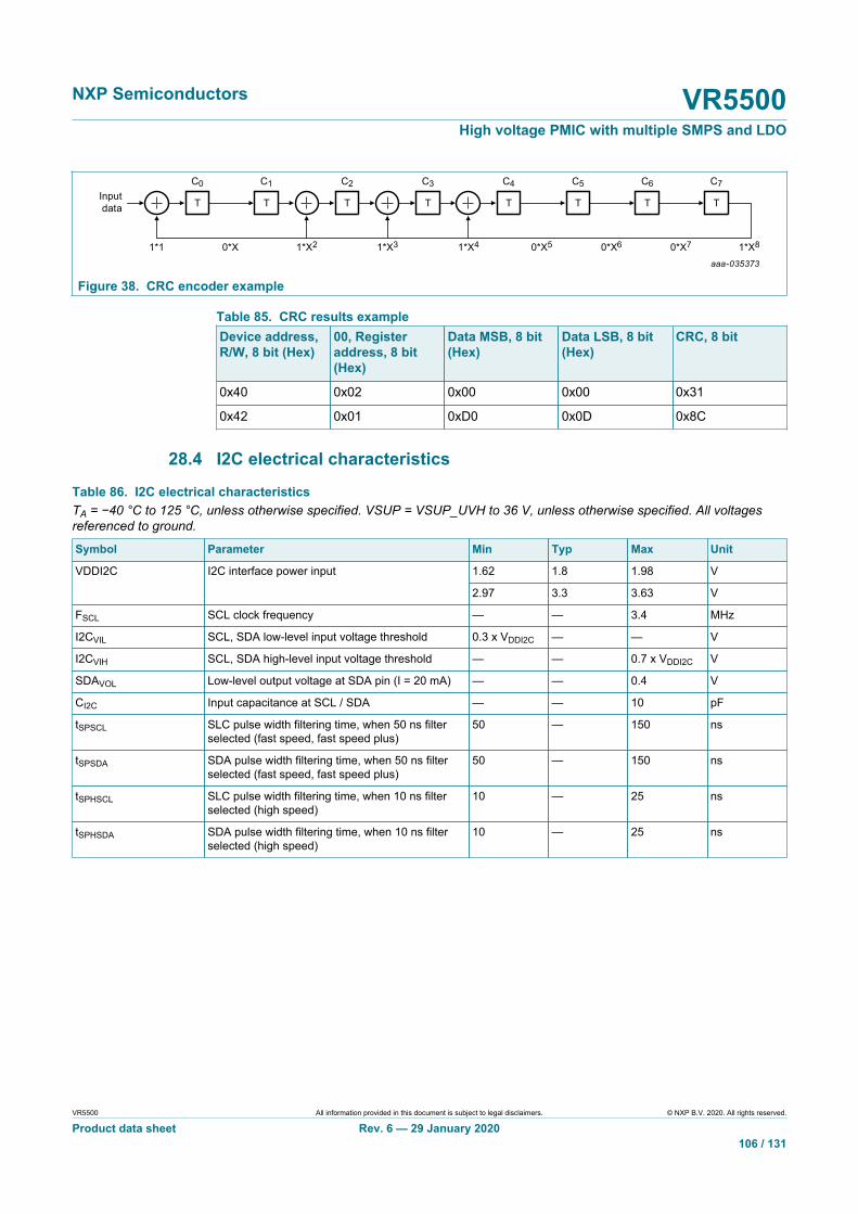
NXP Semiconductors VR5500High voltage PMIC with multiple SMPS and LDO
VR5500 All information provided in this document is subject to legal disclaimers. © NXP B.V. 2020. All rights reserved.
Product data sheet Rev. 6 — 29 January 2020106 / 131
aaa-035373
T
C0
1*1 0*X 1*X2 1*X3 1*X4 0*X5 0*X6 0*X7 1*X8
Inputdata T
C2
T
C3
T
C4
T
C1
T
C5
T
C6
T
C7
Figure 38. CRC encoder example
Table 85. CRC results exampleDevice address,R/W, 8 bit (Hex)
00, Registeraddress, 8 bit(Hex)
Data MSB, 8 bit(Hex)
Data LSB, 8 bit(Hex)
CRC, 8 bit
0x40 0x02 0x00 0x00 0x31
0x42 0x01 0xD0 0x0D 0x8C
28.4 I2C electrical characteristics
Table 86. I2C electrical characteristicsTA = −40 °C to 125 °C, unless otherwise specified. VSUP = VSUP_UVH to 36 V, unless otherwise specified. All voltagesreferenced to ground.
Symbol Parameter Min Typ Max Unit
1.62 1.8 1.98 VVDDI2C I2C interface power input
2.97 3.3 3.63 V
FSCL SCL clock frequency — — 3.4 MHz
I2CVIL SCL, SDA low-level input voltage threshold 0.3 x VDDI2C — — V
I2CVIH SCL, SDA high-level input voltage threshold — — 0.7 x VDDI2C V
SDAVOL Low-level output voltage at SDA pin (I = 20 mA) — — 0.4 V
CI2C Input capacitance at SCL / SDA — — 10 pF
tSPSCL SLC pulse width filtering time, when 50 ns filterselected (fast speed, fast speed plus)
50 — 150 ns
tSPSDA SDA pulse width filtering time, when 50 ns filterselected (fast speed, fast speed plus)
50 — 150 ns
tSPHSCL SLC pulse width filtering time, when 10 ns filterselected (high speed)
10 — 25 ns
tSPHSDA SDA pulse width filtering time, when 10 ns filterselected (high speed)
10 — 25 ns

NXP Semiconductors VR5500High voltage PMIC with multiple SMPS and LDO
VR5500 All information provided in this document is subject to legal disclaimers. © NXP B.V. 2020. All rights reserved.
Product data sheet Rev. 6 — 29 January 2020107 / 131
29 Application information
VR5500BUCK1 and 2 can operate in multiphaseBUCK3_IN can be VPRE or VBOOSTLDO1_IN can be VPRE or VBOOST
VDDIO input can be LDOx, VPRE or otherVDDI2C input can be LDOx, VPRE or other
VMON1 is compared to 0.8 VWAKE1 global and WAKE2 local in this example
aaa-032953
47 F
1 H
1 H
100 nF
1 nF
6.8 nF
5.1 kΩ
1 MΩ1 MΩ
10 mΩ
5.1 kΩ
5.1 kΩ
5.1 kΩ
100 kΩ
VSUP1 BOOST_LS
LDO1_IN
PSYNC
BUCK2-FB
BUCK2-SW
BUCK1-FB
BUCK1-SW
VDDI2CVDDIOLDO2
VCOREMON
3.3 V
VCORE
ADC_REF
ADC_IN
RESET
POR
VBOOST
single package decoulping capacitors close to device pin
PRE
_GH
S
PRE
_GLS
PRE
_BO
OT
PRE
_SW
VBAT
VSUP2
WAKE1
VBOS
10 F
22 nF
2 x 10 F 60 F
22 F
100 nF
40 F/100 nF
40 F/100 nF
10 F 100 nF
10 nF
4.7 F 100 nF 1 nF47 nF
6.8 H
4.7 H
1 H
1 H
10 nF
22 nF 5 V
WAKE2
DBG
Wake up source
To ext IC
To synch ext IC with FIN
Independent voltagemonitoring from VR5500
or other regulators
I2C communication(for OTP programming)
VDDI2C
VDDI2C
10 F100 nF
LDO15 V
BUCK3-FB
SDA
SCL
BUCK3-SW
CAN4.7 F
40 F/100 nF
100 nF
FOUT
VMON1220 ΩAMUX
MCU
GN
D
ePAD
5.1 kΩVDDIOPGOOD
INTB
FIN
5.1 kΩ
5.1 kΩ
VDDIO
VBOS
RSTB
PRE
_CSP
PRE
_FB
PRE
_CO
MP
BUC
K1-
IN
BUCK1-INVPRE
4.7 F 100 nF
BUCK2-IN
4.7 F 100 nF
BUCK3-IN
RSTB
1 nF
PGOOD
1 nF
INTB
100 nF
VDDIO
100 nF
VDDI2C
BUC
K2-
IN
BUC
K3-
IN
BUC
K3-
INQ
Figure 39. VR5500 application diagram
30 Fail-safe domain description
30.1 Functional descriptionThe fail-safe domain is electrically independent and physically isolated. The fail-safedomain is supplied by its own reference voltages and current, has its own oscillator.
The fail-safe domain and the dedicated pins are represented in Figure 40:

NXP Semiconductors VR5500High voltage PMIC with multiple SMPS and LDO
VR5500 All information provided in this document is subject to legal disclaimers. © NXP B.V. 2020. All rights reserved.
Product data sheet Rev. 6 — 29 January 2020108 / 131
aaa-032954
Vdig_FS OTPFAIL-SAFE STATE MACHINE PGOODDRIVER
RESETDRIVER
VOLTAGESUPERVISION
VDDIO
Vdig_FS
VMON1
VCOREMON
PGOOD
RSTBOSCFS
I2CFS
VMON1
Figure 40. Fail-safe block diagram
30.2 Voltage supervisorThe voltage supervisor is in charge of overvoltage and undervoltage monitoring ofVCOREMON, VDDIO and VMON1 input pins. When an overvoltage occurs on a VR5500regulator monitored by one of these pins, the associated VR5500 regulator is switchedoff till the fault is removed. The voltage monitoring is active as soon as FS_ENABLE=1and UV/OV flags are then reported accordingly.
30.2.1 VCOREMON monitoring
VCOREMON input pin is dedicated to BUCK1 or BUCK1 and BUCK2, in case ofmultiphase operation. When overvoltage or undervoltage fault is detected, the fail-safereaction on RSTB is configurable with the VCOREMON_OV/UV_FS_IMPACT[1:0] bitsduring the INIT_FS phase.
Table 87. VCOREMON error impact configurationVCOREMON_OV_FS_IMPACT[1:0] VCOREMON OV impact on RSTB
00 No effect on RSTB
01 Reserved
1x (default) RSTB is asserted
Reset condition POR
VCOREMON_UV_FS_IMPACT[1:0] VCOREMON UV impact on RSTB
00 No effect on RSTB
01 (default) No effect on RSTB
1x RSTB is asserted
Reset condition POR

NXP Semiconductors VR5500High voltage PMIC with multiple SMPS and LDO
VR5500 All information provided in this document is subject to legal disclaimers. © NXP B.V. 2020. All rights reserved.
Product data sheet Rev. 6 — 29 January 2020109 / 131
Table 88. VCOREMON electrical characteristicsTA = −40 °C to 125 °C, unless otherwise specified. VSUP = VSUP_UVH to 36 V, unless otherwise specified. All voltagesreferenced to ground.
Symbol Parameter Min Typ Max Unit
VCOREMON_OV_min Overvoltage threshold minimum — +4.5 — %
VCOREMON_OV_max Overvoltage threshold maximum — +12 — %
VCOREMON_OV_step Overvoltage threshold step (OTP_VCOREOVTH[7:0] bits)
— +0.5 — %
VCOREMON_OV_acc Overvoltage threshold accuracy −2 — 2 %
20 25 30 μsTCOREMON_OV Overvoltage filtering time (OTP_VCORE_OV_DGLT bit)
40 45 50 μs
VCOREMON_UV_min Undervoltage threshold minimum — −4.5 — %
VCOREMON_UV_max Undervoltage threshold maximum — −12 — %
VCOREMON_UV_step Undervoltage threshold step (OTP_VCOREUVTH[7:0] bits)
— −0.5 — %
VCOREMON_UV_acc Undervoltage threshold accuracy −2 — 2 %
2.5 5 7.5 μs
10 15 20 μs
20 25 30 μs
TCOREMON_UV Undervoltage filtering time (OTP_VCORE_UV_DGLT[1:0] bits)
35 40 45 μs
30.2.2 Static voltage scaling (SVS)
A static voltage scaling function is implemented to allow the MCU to reduce the outputvoltage initially configured at start-up of BUCK1 (and BUCK2 if used in multiphase). TheSVS configuration must be done in INIT_FS phase. The offset value is configurable byI2C with the SVS_OFFSET[4:0] bits and the exact complemented value shall be writtenin the NOT_SVS_OFFSET[4:0] bits.
Table 89. SVS offset configurationSVS_OFFSET[4:0] NOT_SVS_OFFSET[4:0] Offset applied to BUCK1
(and BUCK2 if used inmultiphase)
0 0000 (default) 1 1111 0 mV
0 0001 1 1110 −6.25 mV
... ... −6.25 mV step per bit
1 0000 0 1111 −100 mV
Reset condition POR
The BUCK1/2 output voltage transition starts when the NOT_SVS_OFFSET[4:0] I2Ccommand is received and confirmed good. If the NOT_SVS_OFFSET[4:0] I2C commandis not the exact opposite to the SVS_OFFSET[4:0] I2C command, the SVS procedureis not executed and the BUCK1 output voltage remains at its original value. The OV/UV threshold changes immediately when the NOT_SVS_OFFSET[4:0] I2C command isreceived and confirmed good. Therefore, the BUCK1 output voltage transition is donewithin TCOREMON_OV.

NXP Semiconductors VR5500High voltage PMIC with multiple SMPS and LDO
VR5500 All information provided in this document is subject to legal disclaimers. © NXP B.V. 2020. All rights reserved.
Product data sheet Rev. 6 — 29 January 2020110 / 131
aaa-032959
OV
UV
TCOREMON_OV
VBUCK1 =VCOREMON= 0.75 V
VBUCK1 =VCOREMON
= 0.8 V
I2CFS_I_NOT_SVS
I2CFS_I_SVS
VBUCK12_SVS
Figure 41. SVS principle
30.2.3 VDDIO monitoring
VDDIO input pin can be connected to VPRE, LDO1, LDO2, BUCK3, or an externalregulator. The regulator connected to VDDIO must be at 3.3 V or 5.0 V to be compatiblewith overvoltage and undervoltage monitoring thresholds. In order to turn OFF theregulator in case of overvoltage detection, the configuration of which regulator isconnected to VDDIO is done with OTP_VDDIO_REG_ASSIGN[2:0] bits. If an externalregulator (not delivered by the VR5500) is connected to VDDIO, this regulator cannotbe turned OFF, but the overvoltage flag is reported to the MCU which can takeappropriate action. In all cases, the reaction on RSTB is configured with VDDIO_OV/UV_FS_IMPACT[1:0] bits.
aaa-031023
UV
bandgap_FS
OTP_VDDIOOVTH[3:0]OTP_VDDIOUVTH[3:0]
OTP_VDDIO_V
VDDIO
OV
Figure 42. VDDIO monitoring principle
When overvoltage or undervoltage fault is detected, the fail-safe reaction on RSTB isconfigurable with the VDDIO_OV/UV_IMPACT[1:0] bits during the INIT_FS phase.

NXP Semiconductors VR5500High voltage PMIC with multiple SMPS and LDO
VR5500 All information provided in this document is subject to legal disclaimers. © NXP B.V. 2020. All rights reserved.
Product data sheet Rev. 6 — 29 January 2020111 / 131
Table 90. VDDIO error impact configurationVDDIO_OV_FS_IMPACT[1:0] VDDIO OV impact on RSTB
00 No effect on RSTB
01 Reserved
1x (default) RSTB is asserted
Reset condition POR
VDDIO_UV_FS_IMPACT[1:0] VDDIO UV impact on RSTB
00 No effect on RSTB
01 (default) No effect on RSTB
1x RSTB is asserted
Reset condition POR
Table 91. VDDIO electrical characteristicsTA = −40 °C to 125 °C, unless otherwise specified. VSUP = VSUP_UVH to 36 V, unless otherwise specified. All voltagesreferenced to ground.
Symbol Parameter Min Typ Max Unit
VDDIO_OV_min Overvoltage threshold minimum — +4.5 — %
VDDIO_OV_max Overvoltage threshold maximum — +12 — %
VDDIO_OV_step Overvoltage threshold step (OTP_VDDIOOVTH[7:0] bits)
— +0.5 — %
VDDIO_OV_acc Overvoltage threshold accuracy −2 — 2 %
20 25 30 μsTVDDIO_OV Overvoltage filtering time (OTP_VDDIO_OV_DGLT bit)
40 45 50 μs
VDDIO_UV_min Undervoltage threshold minimum — −4.5 — %
VDDIO_UV_max Undervoltage threshold maximum — −12 — %
VDDIO_UV_step Undervoltage threshold step (OTP_VDDIOUVTH[7:0] bits)
— −0.5 — %
VDDIO_UV_acc Undervoltage threshold accuracy −2 — 2 %
2.5 5 7.5 μs
10 15 20 μs
20 25 30 μs
TVDDIO_UV Undervoltage filtering time (OTP_VDDIO_UV_DGLT[1:0] bits)
35 40 45 μs
30.2.4 VMON1 monitoring
Each VMON1 monitoring feature is enabled by OTP. VMON1 input pin can be connectedto VPRE, LDO1, LDO2, BUCK3, BUCK2 (in case BUCK2 is not used in multiphase),or even an external regulator. In order to turn OFF the regulator in case of Overvoltagedetection, the configuration of which regulator is connected to VMON1 is done by I2C inthe register M_VMON_REGx. If an external regulator (not delivered by the VR5500) isconnected to VMON1, this regulator cannot be turned OFF, but the Overvoltage flag isreported to the MCU which can take appropriate action. In all cases, the fail-safe reactionon RSTB is configured with VMON1_OV/UV_FS_IMPACT[1:0] bits.

NXP Semiconductors VR5500High voltage PMIC with multiple SMPS and LDO
VR5500 All information provided in this document is subject to legal disclaimers. © NXP B.V. 2020. All rights reserved.
Product data sheet Rev. 6 — 29 January 2020112 / 131
aaa-032960
UV
bandgap_FS
OTP_VMON1OVTH[3:0]OTP_VMON1UVTH[3:0]
ext_R1
ext_R2
VREGx
VMON1
OV
Figure 43. VMON1 monitoring principle
The external resistor bridge connected to VMON1 shall be calculated to delivera middle point of 0.8 V. It is recommended to use ±1 % or less resistor accuracy.When overvoltage or undervoltage fault is detected, the fail-safe reaction on RSTB isconfigurable with the VMON1_OV/UV_FS_IMPACT[1:0] bits during the INIT_FS phase.
Table 92. VMON1 error impact configurationVMON1_OV_FS_IMPACT[1:0] VMON1 OV impact on RSTB
00 No effect on RSTB
01 Reserved
1x (default) RSTB is asserted
Reset condition POR
VMON1_UV_FS_IMPACT[1:0] VMON1 UV impact on RSTB
00 No effect on RSTB
01 (default) No effect on RSTB
1x RSTB is asserted
Reset condition POR
Table 93. VMON1 (without ext resistor accuracy) electrical characteristicsTA = −40 °C to 125 °C, unless otherwise specified. VSUP = VSUP_UVH to 36 V, unless otherwise specified. All voltagesreferenced to ground.
Symbol Parameter Min Typ Max Unit
VMON1_OV_min Overvoltage threshold minimum — +4.5 — %
VMON1_OV_max Overvoltage threshold maximum — +12 — %
VMON1_OV_step Overvoltage threshold step (OTP_VMON1OVTH[7:0] bits)
— +0.5 — %
VMON1_OV_acc Overvoltage threshold accuracy −2 — 2 %
20 25 30 μsTMON1_OV Overvoltage filtering time (OTP_VMON1_OV_DGLT bit)
40 45 50 μs
VMON1_UV_min Undervoltage threshold minimum — −4.5 — %
VMON1_UV_max Undervoltage threshold maximum — −12 — %

NXP Semiconductors VR5500High voltage PMIC with multiple SMPS and LDO
VR5500 All information provided in this document is subject to legal disclaimers. © NXP B.V. 2020. All rights reserved.
Product data sheet Rev. 6 — 29 January 2020113 / 131
Symbol Parameter Min Typ Max Unit
VMON1_UV_step Undervoltage threshold step (OTP_VMON1UVTH[7:0] bits)
— −0.5 — %
VMON1_UV_acc Undervoltage threshold accuracy −2 — 2 %
2.5 5 7.5 μs
10 15 20 μs
20 25 30 μs
TMON1_UV Undervoltage filtering time (OTP_VMON1_UV_DGLT[1:0] bits)
35 40 45 μs
VMON1_PD Internal passive pull down 1 2 4 MΩ
30.3 Fault management
30.3.1 Fault source and reaction
In normal operation when RSTB is released, the fault error counter is incremented whena fault is detected by the VR5500 fail-safe state machine. Table 94 lists the faults andtheir impact on PGOOD and RSTB pins according to the device configuration. The faultsthat are configured to not assert RSTB will not increment the fault error counter. In thatcase, only the flags are available for MCU diagnostic.
Table 94. Application related fail-safe fault list and reactionIn Orange, the reaction in not configurable.In Green, the reaction is configurable by OTP for PGOOD and I2C for RSTB during INIT_FS.
Application-related fail-safe faults FLT_ERR_CNTincrement
RSTB assertion PGOOD assertion
VCOREMON_OV +1 VCOREMON_OV_FS_IMPACT[1] OTP config
VDDIO_OV +1 VDDIO_OV_FS_IMPACT[1] OTP config
VMON1_OV +1 VMON1_OV_FS_IMPACT[1] OTP config
VCOREMON_UV +1 VCOREMON_UV_FS_IMPACT[1] OTP config
VDDIO_UV +1 VDDIO_UV_FS_IMPACT[1] OTP config
VMON1_UV +1 VMON1_UV_FS_IMPACT[1] OTP config
External RESET (out of extendedRSTB)
+1 Yes (low externally) No
RSTB pulse request by MCU No Yes No
RSTB short to high +1 No (high externally) No
REG_CORRUPT = 1 +1 No No
OTP_CORRUPT = 1 +1 No No
If OTP_PGOOD_RSTB = '0' (default configuration), RSTB and PGOOD pins workindependently according to Table 94. If OTP_PGOOD_RSTB = '1', RSTB and PGOODpins work concurrently and all the faults asserting RSTB will also assert PGOOD.
30.3.2 Fault error counter
The VR5500 integrates a configurable fault error counter which is counting the numberof faults related to the device itself and also caused by external events. The fault errorcounter starts at level '1' after a POR or resuming from Standby. The final value of thefault error counter is used to transition in DEEP-FS mode. The maximum value of this

NXP Semiconductors VR5500High voltage PMIC with multiple SMPS and LDO
VR5500 All information provided in this document is subject to legal disclaimers. © NXP B.V. 2020. All rights reserved.
Product data sheet Rev. 6 — 29 January 2020114 / 131
counter is configurable with the FLT_ERR_CNT_LIMIT[1:0] bits during the INIT_FSphase.
Table 95. Fault error counter configurationFLT_ERR_CNT_LIMIT[1:0] Fault error counter max value configuration
00 2
01 (default) 6
10 8
11 12
Reset condition POR
30.4 PGOOD, RSTBThese two output pins have a hierarchical implementation in order to guarantee the safestate.
• PGOOD has the priority one. If PGOOD is asserted, RSTB is asserted.• RSTB has the priority two. If RSTB is asserted, PGOOD may not be asserted.
30.4.1 PGOOD
PGOOD is an open-drain output that can be connected in the application to the PORB ofthe MCU. PGOOD requires an external pull-up resistor to VDDIO and a filtering capacitorto GND for immunity. An internal pull-down RPD ensures PGOOD low-level in Standbyand Power down mode. VCOREMON, VDDIO, VMON1 can be assigned to PGOOD byOTP.
PGOOD is asserted low by the FS_LOGIC when any of the assigned regulators are inundervoltage or overvoltage. When PGOOD is asserted low, RSTB is also asserted low.An internal pull-up on the gate of the low-side MOS ensures PGOOD low-level in case ofFS_LOGIC failure.
aaa-031028
FS_LOGIC
VSUP PGOOD to MCU PORB
VDDIO
RPD
5.1 kΩ
1 nF
Figure 44. PGOOD pin implementation

NXP Semiconductors VR5500High voltage PMIC with multiple SMPS and LDO
VR5500 All information provided in this document is subject to legal disclaimers. © NXP B.V. 2020. All rights reserved.
Product data sheet Rev. 6 — 29 January 2020115 / 131
Table 96. PGOOD electrical characteristicsTA = −40 °C to 125 °C, unless otherwise specified. VSUP = VSUP_UVH to 36 V, unless otherwise specified. All voltagesreferenced to ground.
Symbol Parameter Min Typ Max Unit
PGOODVIL Low-level input voltage threshold 1.0 — — V
PGOODVIH High-level input voltage threshold — — 2.0 V
PGOODHYST Input voltage hysteresis 100 — — mV
PGOODVOL Low-level output voltage (I = 2.0 mA) — — 0.5 V
PGOODRPD Internal pull-down resistor 200 400 800 kΩ
PGOODILIM Current limitation 4.0 — 20 mA
PGOODTFB Feedback filtering time 8.0 — 15 μs
30.4.2 RSTB
RSTB is an open-drain output that can be connected in the application to the RESET ofthe MCU. RSTB requires an external pull-up resistor to VDDIO and a filtering capacitorto GND for immunity. An internal pull-down RPD ensures RSTB low level in Standby andPower down mode. RSTB assertion depends on the device configuration during INIT_FSphase. An internal pull up on the gate of the low-side MOS ensures RSTB low level incase of FS_LOGIC failure. When RSTB is stuck low for more than RSTBT8S, the devicetransitions in DEEP-FS mode.
aaa-031029
FS_LOGIC
VSUP RSTB to MCU reset
VDDIO
RPD
5.1 kΩ
1 nF
Figure 45. RSTB pin implementation
NXP Semiconductors VR5500High voltage PMIC with multiple SMPS and LDO
VR5500 All information provided in this document is subject to legal disclaimers. © NXP B.V. 2020. All rights reserved.
Product data sheet Rev. 6 — 29 January 2020116 / 131
Table 97. RSTB electrical characteristicsTA = −40 °C to 125 °C, unless otherwise specified. VSUP = VSUP_UVH to 36 V, unless otherwise specified. All voltagesreferenced to ground.
Symbol Parameter Min Typ Max Unit
RSTBVIL Low-level input voltage threshold 1.0 — — V
RSTBVIH High-level input voltage threshold — — 2.0 V
RSTBHYST Input voltage hysteresis 100 — — mV
RSTBVOL Low-level output voltage (I = 2.0 mA) — — 0.5 V
RSTBRPB Internal pull-down resistor 200 400 800 kΩ
RSTBILIM Current limitation 4.0 — 20 mA
RSTBTFB Feedback filtering time 8.0 — 15 μs
RSTBTSC Short to high filtering time 500 — 800 us
RSTBTLG Long pulse (configurable with RSTB_DUR bit) 9.0 — 11 ms
RSTBTST Short pulse (configurable with RSTB_DUR bit) 0.9 — 1.1 ms
RSTBT8S 8 second timer 7.0 8.0 9.0 s
RSTBTRELEASE Time to release RSTB from wake-up or POR withall regulators started in Slot 0
— 8.0 — ms
31 Package information
VR5500 package is a QFN (sawn), thermally enhanced wettable flanks, 8 x 8 x 0.85 mm,0.5 mm pitch, 56 pins. The assembly can be done at two different NXP assembly siteswith slight wettable flank difference but sharing the same PCB footprint.
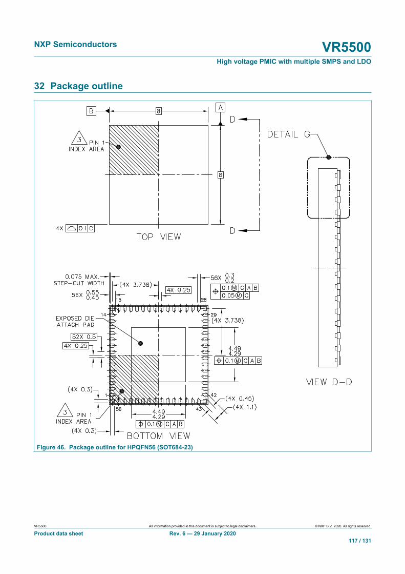
NXP Semiconductors VR5500High voltage PMIC with multiple SMPS and LDO
VR5500 All information provided in this document is subject to legal disclaimers. © NXP B.V. 2020. All rights reserved.
Product data sheet Rev. 6 — 29 January 2020117 / 131
32 Package outline
Figure 46. Package outline for HPQFN56 (SOT684-23)

NXP Semiconductors VR5500High voltage PMIC with multiple SMPS and LDO
VR5500 All information provided in this document is subject to legal disclaimers. © NXP B.V. 2020. All rights reserved.
Product data sheet Rev. 6 — 29 January 2020118 / 131
Figure 47. Package outline detail for HPQFN56 (SOT684-23)
Figure 48. Package outline notes for HPQFN56 (SOT684-23)

NXP Semiconductors VR5500High voltage PMIC with multiple SMPS and LDO
VR5500 All information provided in this document is subject to legal disclaimers. © NXP B.V. 2020. All rights reserved.
Product data sheet Rev. 6 — 29 January 2020119 / 131
33 Layout and PCB guidelines
33.1 Landing pad information
Figure 49. Solder mask pattern
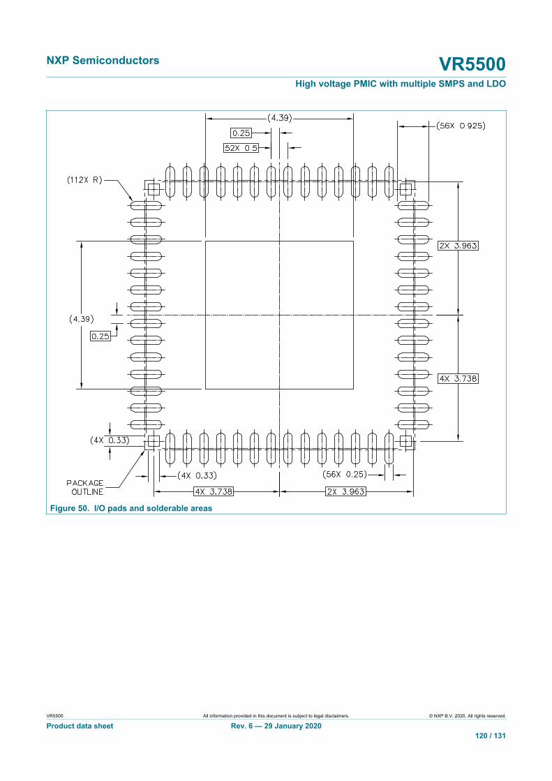
NXP Semiconductors VR5500High voltage PMIC with multiple SMPS and LDO
VR5500 All information provided in this document is subject to legal disclaimers. © NXP B.V. 2020. All rights reserved.
Product data sheet Rev. 6 — 29 January 2020120 / 131
Figure 50. I/O pads and solderable areas

NXP Semiconductors VR5500High voltage PMIC with multiple SMPS and LDO
VR5500 All information provided in this document is subject to legal disclaimers. © NXP B.V. 2020. All rights reserved.
Product data sheet Rev. 6 — 29 January 2020121 / 131
Figure 51. Solder paste stencil
33.2 Component selection• SMPS input and output capacitors shall be chosen with low ESR (ceramic or MLCC
type of capacitors). X7R ceramic type is preferred. Input decoupling capacitors shall beplaced as close as possible to the device pin. Output capacitor voltage rating shall beselected to be 3x the voltage output value to minimize the DC bias degradation.
• SMPS inductors shall be shielded with ISAT higher than maximum inductor peakcurrent.
33.3 VPRE• Inductor charging and discharging current loop is designed as small as possible.• Input decoupling capacitors are placed close to the high-side drain transistor pin.• The boot strap capacitor is placed close to the device pin using wide and short track to
connect to the external low-side drain transistor.

NXP Semiconductors VR5500High voltage PMIC with multiple SMPS and LDO
VR5500 All information provided in this document is subject to legal disclaimers. © NXP B.V. 2020. All rights reserved.
Product data sheet Rev. 6 — 29 January 2020122 / 131
• PRE_GLS, PRE_GHS and PRE_SW tracks is wide and short and should not cross anysensitive signal (current sensing, for example).
aaa-032961
L1 connection
implementationNote : L2 is system ground.
VR5500L3 connection
1 2 3 4PR
E_G
HS
PRE_
SWPR
E_G
LS
• PRE_FB used as voltage feedback and current sense shall be connected to RSHUNT
and routed as a pair with CSP.
aaa-032962
layout as a pairdo not cross any noisy signal
VR5500
GND
coil wire
gound plane(and no sxxxx and pair)
GND
CSP
PRE_
FB
• The external transistor thermal shape should be in the range of 25 x 25 mm for
optimum Rth.• The LFPAK56 application note can give better insight: http://assets.nexperia.com/
documents/application-note/AN10874.pdf
33.4 VBUCKx• Inductor charging and discharging current loop is designed as small as possible.
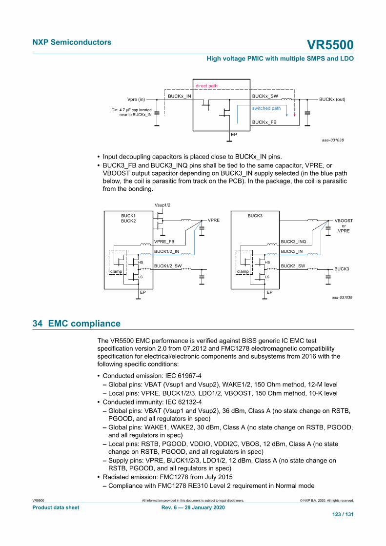
NXP Semiconductors VR5500High voltage PMIC with multiple SMPS and LDO
VR5500 All information provided in this document is subject to legal disclaimers. © NXP B.V. 2020. All rights reserved.
Product data sheet Rev. 6 — 29 January 2020123 / 131
aaa-031038
BUCKx_IN BUCKx_SW
EP
switched path
direct path
Vpre (in) BUCKx (out)
Cin: 4.7 µF cap locatednear to BUCKx_IN
BUCKx_FB
• Input decoupling capacitors is placed close to BUCKx_IN pins.• BUCK3_FB and BUCK3_INQ pins shall be tied to the same capacitor, VPRE, or
VBOOST output capacitor depending on BUCK3_IN supply selected (in the blue pathbelow, the coil is parasitic from track on the PCB). In the package, the coil is parasiticfrom the bonding.
aaa-031039
BUCK1BUCK2
VPRE_FB
Vsup1/2
VPRE
BUCK1/2_IN
BUCK1/2_SW
EP
clamp
HS
LS
BUCK3
BUCK3_INQ
VBOOSTor
VPRE
BUCK3
BUCK3_IN
BUCK3_SW
EP
clamp
HS
LS
34 EMC compliance
The VR5500 EMC performance is verified against BISS generic IC EMC testspecification version 2.0 from 07.2012 and FMC1278 electromagnetic compatibilityspecification for electrical/electronic components and subsystems from 2016 with thefollowing specific conditions:
• Conducted emission: IEC 61967-4– Global pins: VBAT (Vsup1 and Vsup2), WAKE1/2, 150 Ohm method, 12-M level– Local pins: VPRE, BUCK1/2/3, LDO1/2, VBOOST, 150 Ohm method, 10-K level
• Conducted immunity: IEC 62132-4– Global pins: VBAT (Vsup1 and Vsup2), 36 dBm, Class A (no state change on RSTB,
PGOOD, and all regulators in spec)– Global pins: WAKE1, WAKE2, 30 dBm, Class A (no state change on RSTB, PGOOD,
and all regulators in spec)– Local pins: RSTB, PGOOD, VDDIO, VDDI2C, VBOS, 12 dBm, Class A (no state
change on RSTB, PGOOD, and all regulators in spec)– Supply pins: VPRE, BUCK1/2/3, LDO1/2, 12 dBm, Class A (no state change on
RSTB, PGOOD, and all regulators in spec)• Radiated emission: FMC1278 from July 2015
– Compliance with FMC1278 RE310 Level 2 requirement in Normal mode

NXP Semiconductors VR5500High voltage PMIC with multiple SMPS and LDO
VR5500 All information provided in this document is subject to legal disclaimers. © NXP B.V. 2020. All rights reserved.
Product data sheet Rev. 6 — 29 January 2020124 / 131
• Radiated immunity: FMC1278 from July 2015– Injection level per FMC1278 RI112 Level 2 requirement in Normal mode,– Injection level per FMC1278 RI112 Level 2 requirement in Normal mode,– No wake up when injecting FMC1278 RI112 Level 2 requirement in Standby mode
Table 98. Regulators setup for the EMC testsOutput voltage 3.3 V
Switching frequency 455 kHz
VPRE
Output current 3 A
Output voltage 1.25 V
Switching frequency 2.22 MHz
BUCK1
Output current 1.2 A
Output voltage 0.8 V
Switching frequency 2.22 MHz
BUCK2
Output current 1.2 A
Output voltage 2.3 V
Switching frequency 2.22 MHz
BUCK3
Output current 1.2 A
Output voltage 5 V
Switching frequency 2.22 MHz
BOOST
Output current 275 mA
Output voltage 2.5 VLDO1
Output current 75 mA
Output voltage 1.1 VLDO2
Output current 200 mA
35 References
[1] VR5500_PDTCALC[1] — VPRE compensation network calculation and power dissipation tool (Excel file)
[2] VR5500_OTP_Mapping[1] — OTP programming configuration (Excel file)
[3] VR5500_VPRE_Simplis_Model[1] — Simplis model for stability and transient simulations
[4] Schematic[1] — Reference schematic in Cadence and PDF formats
[5] Layout[1] — Reference layout in Cadence format
[6] EVB[1] — Evaluation board (EVB)
[7] FlexGUI[1] — Graphical user interface to be used with the EVB
[1] Contact NXP sales representative.

NXP Semiconductors VR5500High voltage PMIC with multiple SMPS and LDO
VR5500 All information provided in this document is subject to legal disclaimers. © NXP B.V. 2020. All rights reserved.
Product data sheet Rev. 6 — 29 January 2020125 / 131
36 Revision historyTable 99. Revision historyDocument ID Release date Data sheet status Change notice Supersedes
VR5500 v.6.0 20200129 Product data sheet 201912015I VR5500 v.5.0
Modifications • Global: deleted "SPI" references• Section 15: corrrected typo (deleted R/W SPI column)
VR5500 v.5.0 20191218 Product data sheet 201912015I VR5500 v.4.0
Modifications • Global: changed document status from "Preliminary" to "Product"
VR5500 v.4.0 20191216 Preliminary data sheet 201912015I VR5500 v.3.0
Modifications • Global: multiple formatting and wording updates• Table 1: added OTP ID• Table 2: updated ground pin description• Table 4: added values for BUCKx_SW and updated min value for DC voltage (replaced −1.0 by −0.3)• Table 5: updated TA and TJ description (added "Grade1")• Table 7: updated TDBG values and unit• Table 8, Table 12: replaced "GOTOSTBY" by "GoToSTBY"• Table 19: updated description for RATIO• Table 26: updated reset value for Bit 22 and Bit 23 (replaced 0 by 1)• Table 54: updated reset value for Bit 17 and Bit 22 (replaced 0 by 1)• Table 64: updated OTP_CFG_BUCK1_2 and OTP_CFG_BUCK2_2 register description (replaced 2.6 A by Reserved)• Table 65: updated OTP_CFG_UVOV_3 register description• Table 66, Table 67, Table 70, Table 76, Table 72, Table 71: updated parameters• Figure 8: replaced "WAKE1" by "WAKE1/2"• Section 10: updated description for charged device model• Section 11: updated assumptions and description (replaced "VFPRE_SW" by "FPRE_SW")• Section 20.5: updated description and values in Table 68• Section 20.6: updated Figure 14• Section 22.6: updated Figure 22• Section 23.5: updated Figure 26• Section 25.1: replaced "VPRE switching frequency is coming from CLK2 (455 kHz)" by "VPRE switching frequency is
coming from CLK2 (455 kHz) or CLK1 (2.22 MHz)"• Section 27.4: updated figure title and description• Section 28.3: enhanced description (added Figure 38 and Table 85)• Section 30.4.1, Section 30.4.2: updated current limiting parameters• Section 33.3, Section 33.4: updated description
VR5500 v.3.0 20190522 Preliminary data sheet - VR5500 v.2.0
Modifications • Global: deleted safety references throughout the document• Section 30: updated section title (replaced "Functional safety" by "Fail-safe domain description")
VR5500 v.2.0 20190415 Preliminary data sheet - VR5500 v.1.0
Modifications • Global: changed document status from Objective to Preliminary• Table 1: replaced MC by PC• Table 4: added parameters for BUCKx_IN• Section 10: updated description• Section 11: updated Figure 4, assumptions, and description• Section 15: renamed column R/W to R/W SPI and added a column R/W I2C• Table 64: replaced CLK_DIV1 by 2.22 MHz• Table 64: updated the value and description for OTP_CFG_CLOCK_4 register bit 3 (replaced 0 by 1 and 2.22 MHz by 455
kHz)• Section 20.1: replaced "VSUP = VPRE / (TPRE_ON_MIN × VPRE_SW)" by "VSUP = LPI_DCR × IPRE + VPRE_UVL / DMAX with DMAX =
1 − (VPRE_SW × TPRE_OFF_MIN)"• Figure 14: deleted 2.22 MHz curves
VR5500 v.1.0 20190221 Objective data sheet - -

NXP Semiconductors VR5500High voltage PMIC with multiple SMPS and LDO
VR5500 All information provided in this document is subject to legal disclaimers. © NXP B.V. 2020. All rights reserved.
Product data sheet Rev. 6 — 29 January 2020126 / 131
37 Legal information
37.1 Data sheet status
Document status[1][2] Product status[3] Definition
Objective [short] data sheet Development This document contains data from the objective specification for productdevelopment.
Preliminary [short] data sheet Qualification This document contains data from the preliminary specification.
Product [short] data sheet Production This document contains the product specification.
[1] Please consult the most recently issued document before initiating or completing a design.[2] The term 'short data sheet' is explained in section "Definitions".[3] The product status of device(s) described in this document may have changed since this document was published and may differ in case of multiple
devices. The latest product status information is available on the Internet at URL http://www.nxp.com.
37.2 DefinitionsDraft — The document is a draft version only. The content is still underinternal review and subject to formal approval, which may result inmodifications or additions. NXP Semiconductors does not give anyrepresentations or warranties as to the accuracy or completeness ofinformation included herein and shall have no liability for the consequencesof use of such information.
Short data sheet — A short data sheet is an extract from a full data sheetwith the same product type number(s) and title. A short data sheet isintended for quick reference only and should not be relied upon to containdetailed and full information. For detailed and full information see therelevant full data sheet, which is available on request via the local NXPSemiconductors sales office. In case of any inconsistency or conflict with theshort data sheet, the full data sheet shall prevail.
Product specification — The information and data provided in a Productdata sheet shall define the specification of the product as agreed betweenNXP Semiconductors and its customer, unless NXP Semiconductors andcustomer have explicitly agreed otherwise in writing. In no event however,shall an agreement be valid in which the NXP Semiconductors productis deemed to offer functions and qualities beyond those described in theProduct data sheet.
37.3 DisclaimersLimited warranty and liability — Information in this document is believedto be accurate and reliable. However, NXP Semiconductors does notgive any representations or warranties, expressed or implied, as to theaccuracy or completeness of such information and shall have no liabilityfor the consequences of use of such information. NXP Semiconductorstakes no responsibility for the content in this document if provided by aninformation source outside of NXP Semiconductors. In no event shall NXPSemiconductors be liable for any indirect, incidental, punitive, special orconsequential damages (including - without limitation - lost profits, lostsavings, business interruption, costs related to the removal or replacementof any products or rework charges) whether or not such damages are basedon tort (including negligence), warranty, breach of contract or any otherlegal theory. Notwithstanding any damages that customer might incur forany reason whatsoever, NXP Semiconductors’ aggregate and cumulativeliability towards customer for the products described herein shall be limitedin accordance with the Terms and conditions of commercial sale of NXPSemiconductors.
Right to make changes — NXP Semiconductors reserves the right tomake changes to information published in this document, including withoutlimitation specifications and product descriptions, at any time and without
notice. This document supersedes and replaces all information supplied priorto the publication hereof.
Applications — Applications that are described herein for any of theseproducts are for illustrative purposes only. NXP Semiconductors makesno representation or warranty that such applications will be suitablefor the specified use without further testing or modification. Customersare responsible for the design and operation of their applications andproducts using NXP Semiconductors products, and NXP Semiconductorsaccepts no liability for any assistance with applications or customer productdesign. It is customer’s sole responsibility to determine whether the NXPSemiconductors product is suitable and fit for the customer’s applicationsand products planned, as well as for the planned application and use ofcustomer’s third party customer(s). Customers should provide appropriatedesign and operating safeguards to minimize the risks associated withtheir applications and products. NXP Semiconductors does not accept anyliability related to any default, damage, costs or problem which is basedon any weakness or default in the customer’s applications or products, orthe application or use by customer’s third party customer(s). Customer isresponsible for doing all necessary testing for the customer’s applicationsand products using NXP Semiconductors products in order to avoid adefault of the applications and the products or of the application or use bycustomer’s third party customer(s). NXP does not accept any liability in thisrespect.
Limiting values — Stress above one or more limiting values (as defined inthe Absolute Maximum Ratings System of IEC 60134) will cause permanentdamage to the device. Limiting values are stress ratings only and (proper)operation of the device at these or any other conditions above thosegiven in the Recommended operating conditions section (if present) or theCharacteristics sections of this document is not warranted. Constant orrepeated exposure to limiting values will permanently and irreversibly affectthe quality and reliability of the device.
Terms and conditions of commercial sale — NXP Semiconductorsproducts are sold subject to the general terms and conditions of commercialsale, as published at http://www.nxp.com/profile/terms, unless otherwiseagreed in a valid written individual agreement. In case an individualagreement is concluded only the terms and conditions of the respectiveagreement shall apply. NXP Semiconductors hereby expressly objects toapplying the customer’s general terms and conditions with regard to thepurchase of NXP Semiconductors products by customer.
No offer to sell or license — Nothing in this document may be interpretedor construed as an offer to sell products that is open for acceptance orthe grant, conveyance or implication of any license under any copyrights,patents or other industrial or intellectual property rights.
Suitability for use in automotive applications — This NXPSemiconductors product has been qualified for use in automotiveapplications. Unless otherwise agreed in writing, the product is not designed,authorized or warranted to be suitable for use in life support, life-critical orsafety-critical systems or equipment, nor in applications where failure ormalfunction of an NXP Semiconductors product can reasonably be expected

NXP Semiconductors VR5500High voltage PMIC with multiple SMPS and LDO
VR5500 All information provided in this document is subject to legal disclaimers. © NXP B.V. 2020. All rights reserved.
Product data sheet Rev. 6 — 29 January 2020127 / 131
to result in personal injury, death or severe property or environmentaldamage. NXP Semiconductors and its suppliers accept no liability forinclusion and/or use of NXP Semiconductors products in such equipment orapplications and therefore such inclusion and/or use is at the customer's ownrisk.
Export control — This document as well as the item(s) described hereinmay be subject to export control regulations. Export might require a priorauthorization from competent authorities.
Translations — A non-English (translated) version of a document is forreference only. The English version shall prevail in case of any discrepancybetween the translated and English versions.
37.4 TrademarksNotice: All referenced brands, product names, service names andtrademarks are the property of their respective owners.
NXP — is a trademark of NXP B.V.

NXP Semiconductors VR5500High voltage PMIC with multiple SMPS and LDO
VR5500 All information provided in this document is subject to legal disclaimers. © NXP B.V. 2020. All rights reserved.
Product data sheet Rev. 6 — 29 January 2020128 / 131
TablesTab. 1. Ordering information ..........................................2Tab. 2. Pin description ...................................................4Tab. 3. Connection of unused pins ............................... 6Tab. 4. Maximum ratings ...............................................8Tab. 5. Thermal ratings ................................................. 9Tab. 6. Electrical characteristics ..................................10Tab. 7. Electrical characteristics ..................................15Tab. 8. Main writing registers overview ....................... 17Tab. 9. Main reading registers overview ......................18Tab. 10. M_FLAG register bit allocation ........................18Tab. 11. M_FLAG register bit description ......................19Tab. 12. M_MODE register bit allocation ...................... 20Tab. 13. M_MODE register bit description .................... 20Tab. 14. M_REG_CTRL1 register bit allocation ............ 21Tab. 15. M_REG_CTRL1 register bit description .......... 21Tab. 16. M_REG_CTRL2 register bit allocation ............ 23Tab. 17. M_REG_CTRL2 register bit description .......... 23Tab. 18. M_AMUX register bit allocation .......................25Tab. 19. M_AMUX register bit description .....................25Tab. 20. M_CLOCK register bit allocation .....................25Tab. 21. M_CLOCK register bit description ...................25Tab. 22. M_INT_MASK1 register bit allocation ..............26Tab. 23. M_INT_MASK1 register bit description ........... 27Tab. 24. M_INT_MASK2 register bit allocation ..............28Tab. 25. M_INT_MASK2 register bit description ........... 28Tab. 26. M_FLAG1 register bit allocation ......................30Tab. 27. M_FLAG1 register bit description ....................30Tab. 28. M_FLAG2 register bit allocation ......................32Tab. 29. M_FLAG2 register bit description ....................32Tab. 30. M_VMON_REG1 register bit allocation ........... 34Tab. 31. M_VMON_REG1 register bit description .........34Tab. 32. M_LVB1_SVS register bit allocation ............... 34Tab. 33. M_LVB1_SVS register bit description ............. 35Tab. 34. M_MEMORY0 register bit allocation ............... 35Tab. 35. M_MEMORY0 register bit description ............. 35Tab. 36. M_MEMORY1 register bit allocation ............... 36Tab. 37. M_MEMORY1 register bit description ............. 36Tab. 38. M_DEVICEID register bit allocation ................ 36Tab. 39. M_DEVICEID register bit description .............. 36Tab. 40. Fail-safe writing registers overview ................. 37Tab. 41. Fail-safe reading registers overview ................38Tab. 42. FS_GRL_FLAGS register bit allocation ...........38Tab. 43. FS_GRL_FLAGS register bit description .........39Tab. 44. FS_I_OVUV_SAFE_REACTION1 register
bit allocation .................................................... 39Tab. 45. FS_I_OVUV_SAFE_REACTION1 register
bit description .................................................. 39Tab. 46. FS_I_OVUV_SAFE_REACTION2 register
bit allocation .................................................... 40Tab. 47. FS_I_OVUV_SAFE_REACTION2 register
bit description .................................................. 40Tab. 48. FS_I_FSSM register bit allocation ...................40Tab. 49. FS_I_FSSM register bit description .................40Tab. 50. FS_I_SVS register bit allocation ......................41
Tab. 51. FS_I_SVS register bit description ................... 42Tab. 52. FS_OVUVREG_STATUS register bit
allocation ......................................................... 42Tab. 53. FS_OVUVREG_STATUS register bit
description ....................................................... 43Tab. 54. FS_SAFE_IOS register bit allocation .............. 44Tab. 55. FS_SAFE_IOS register bit description ............ 44Tab. 56. FS_DIAG register bit allocation .......................45Tab. 57. FS_DIAG register bit description .....................45Tab. 58. FS_INTB_MASK register bit allocation ............46Tab. 59. FS_INTB_MASK register bit description ......... 46Tab. 60. FS_STATES register bit allocation ..................46Tab. 61. FS_STATES register bit description ................47Tab. 62. Main OTP_REGISTERS ................................. 48Tab. 63. Fail-safe OTP_REGISTERS ............................49Tab. 64. Main OTP bit description .................................49Tab. 65. Fail-safe OTP bit description ...........................61Tab. 66. Best of supply electrical characteristics ...........67Tab. 67. VPRE electrical characteristics ....................... 71Tab. 68. VPRE external MOSFETs recommendation ....74Tab. 69. Output current capability ................................. 76Tab. 70. VBOOST electrical characteristics .................. 79Tab. 71. BUCK1 and BUCK2 electrical
characteristics ..................................................84Tab. 72. BUCK3 electrical characteristics ..................... 89Tab. 73. LDO1 and LDO2 electrical characteristics .......93Tab. 74. Manual frequency tuning configuration ............95Tab. 75. FOUT multiplexer selection .............................96Tab. 76. Electrical characteristics ..................................97Tab. 77. AMUX output selection ....................................98Tab. 78. AMUX electrical characteristics .......................99Tab. 79. WAKE1, WAKE2 electrical characteristics .... 100Tab. 80. INTB electrical characteristics ....................... 101Tab. 81. List of interrupts from main logic ................... 101Tab. 82. List of interrupts from fail-safe logic ...............102Tab. 83. PSYNC electrical characteristics ...................104Tab. 84. I2C message arrangement ............................105Tab. 85. CRC results example .................................... 106Tab. 86. I2C electrical characteristics ..........................106Tab. 87. VCOREMON error impact configuration ........108Tab. 88. VCOREMON electrical characteristics .......... 109Tab. 89. SVS offset configuration ................................109Tab. 90. VDDIO error impact configuration ................. 111Tab. 91. VDDIO electrical characteristics ....................111Tab. 92. VMON1 error impact configuration ................112Tab. 93. VMON1 (without ext resistor accuracy)
electrical characteristics ................................ 112Tab. 94. Application related fail-safe fault list and
reaction ..........................................................113Tab. 95. Fault error counter configuration ................... 114Tab. 96. PGOOD electrical characteristics ..................115Tab. 97. RSTB electrical characteristics ......................116Tab. 98. Regulators setup for the EMC tests .............. 124Tab. 99. Revision history .............................................125

NXP Semiconductors VR5500High voltage PMIC with multiple SMPS and LDO
VR5500 All information provided in this document is subject to legal disclaimers. © NXP B.V. 2020. All rights reserved.
Product data sheet Rev. 6 — 29 January 2020129 / 131
FiguresFig. 1. Simplified application diagram of VR5500 .........2Fig. 2. Block diagram of VR5500 ................................. 3Fig. 3. Pin configuration for HVQFN56 .........................4Fig. 4. Operating range ................................................ 9Fig. 5. Simplified functional state diagram ..................11Fig. 6. Power sequencing (VREGx PWR_UP) ........... 13Fig. 7. Power-up sequence example ..........................14Fig. 8. Debug mode entry .......................................... 15Fig. 9. VPRE schematic ............................................. 68Fig. 10. Type 2 compensation network concept ...........69Fig. 11. Phase and gain margin simulation .................. 70Fig. 12. Transient response simulation ........................ 71Fig. 13. MOSFET gate charge definition ......................74Fig. 14. VPRE theoretical efficiency .............................75Fig. 15. BOOST schematic ...........................................77Fig. 16. Phase and gain margin simulation .................. 78Fig. 17. Transient response simulation ........................ 79Fig. 18. BUCK1/2 standalone schematic ......................81Fig. 19. BUCK1/2 multiphase schematic ......................82Fig. 20. Phase and gain margin simulation .................. 83Fig. 21. Transient response simulation ........................ 84Fig. 22. BUCK1 and BUCK2 theoretical efficiency ....... 86Fig. 23. BUCK3 schematic ........................................... 87Fig. 24. Phase and gain margin simulation .................. 88Fig. 25. Transient response simulation ........................ 89Fig. 26. BUCK3 theoretical efficiency ...........................91Fig. 27. LDO1 block diagram ....................................... 92Fig. 28. LDO2 block diagram ....................................... 92Fig. 29. Clock management block diagram .................. 94
Fig. 30. BUCK1,2,3_clk = 2.22 MHz without clockphase shifting .................................................. 94
Fig. 31. BUCK1,2,3_clk = 2.22 MHz with clock phaseshifting ............................................................. 95
Fig. 32. AMUX block diagram ...................................... 98Fig. 33. Optional 1.8 V ADC use case ....................... 100Fig. 34. Synchronization of two VR5500 .................... 102Fig. 35. Two VR5500 synchronization timing
diagram ..........................................................103Fig. 36. Synchronization of one VR5500 and one
external PMIC (PF82) ................................... 103Fig. 37. VR5500 and one external PMIC (PF82)
synchronization timing diagram .....................104Fig. 38. CRC encoder example ..................................106Fig. 39. VR5500 application diagram ......................... 107Fig. 40. Fail-safe block diagram ................................. 108Fig. 41. SVS principle .................................................110Fig. 42. VDDIO monitoring principle ...........................110Fig. 43. VMON1 monitoring principle ......................... 112Fig. 44. PGOOD pin implementation ..........................114Fig. 45. RSTB pin implementation ............................. 115Fig. 46. Package outline for HPQFN56 (SOT684-23) . 117Fig. 47. Package outline detail for HPQFN56
(SOT684-23) ..................................................118Fig. 48. Package outline notes for HPQFN56
(SOT684-23) ..................................................118Fig. 49. Solder mask pattern ......................................119Fig. 50. I/O pads and solderable areas ...................... 120Fig. 51. Solder paste stencil .......................................121

NXP Semiconductors VR5500High voltage PMIC with multiple SMPS and LDO
VR5500 All information provided in this document is subject to legal disclaimers. © NXP B.V. 2020. All rights reserved.
Product data sheet Rev. 6 — 29 January 2020130 / 131
Contents1 General description ............................................ 12 Features and benefits .........................................13 Simplified application diagram .......................... 24 Ordering information .......................................... 25 Applications .........................................................26 Block diagram ..................................................... 37 Pinning information ............................................ 47.1 Pinning ...............................................................47.2 Pin description ................................................... 48 Connection of unused pins ................................69 Maximum ratings .................................................810 Electrostatic discharge .......................................810.1 Human body model (JESD22/A114) ..................810.2 Charged device model .......................................810.3 Discharged contact test ..................................... 811 Operating range .................................................. 912 Thermal ratings ................................................... 913 Characteristics .................................................. 1014 Functional description ......................................1014.1 Simplified functional state diagram .................. 1114.2 Main state machine ......................................... 1114.3 Fail-safe state machine ................................... 1214.4 Power sequencing ........................................... 1214.5 Debug mode .................................................... 1415 Register mapping ..............................................1616 Main register mapping ......................................1716.1 Main writing registers overview ....................... 1716.2 Main reading registers overview ......................1816.3 M_FLAG register ............................................. 1816.4 M_MODE register ............................................2016.5 M_REG_CTRL1 register ..................................2116.6 M_REG_CTRL2 register ..................................2316.7 M_AMUX register ............................................ 2516.8 M_CLOCK register .......................................... 2516.9 M_INT_MASK1 register ...................................2616.10 M_INT_MASK2 register ...................................2816.11 M_FLAG1 register ........................................... 3016.12 M_FLAG2 register ........................................... 3216.13 M_VMON_REG1 register ................................ 3416.14 M_LVB1_SVS register .....................................3416.15 M_MEMORY0 register .....................................3516.16 M_MEMORY1 register .....................................3616.17 M_DEVICEID register ......................................3617 Fail-safe register mapping ............................... 3717.1 Fail-safe writing registers overview ..................3717.2 Fail-safe reading registers overview ................ 3817.3 FS_GRL_FLAGS register ................................ 3817.4 FS_I_OVUV_SAFE_REACTION1 register ...... 3917.5 FS_I_OVUV_SAFE_REACTION2 register ...... 4017.6 FS_I_FSSM register ........................................ 4017.7 FS_I_SVS register ...........................................4117.8 FS_OVUVREG_STATUS register ................... 4217.9 FS_SAFE_IOs register .................................... 4417.10 FS_DIAG register ............................................ 4517.11 FS_INTB_MASK register .................................4617.12 FS_STATES register ....................................... 46
18 OTP bits configuration ..................................... 4818.1 Overview ..........................................................4818.2 Main OTP bit description ................................. 4918.3 Fail-safe OTP bit description ........................... 6119 Best of supply ...................................................6619.1 Functional description ......................................6619.2 Best of supply electrical characteristics ........... 6720 High voltage buck: VPRE .................................6720.1 Functional description ......................................6720.2 Application schematic ...................................... 6820.3 Compensation network and stability ................ 6820.4 VPRE electrical characteristics ........................7120.5 VPRE external MOSFETs ............................... 7420.6 VPRE efficiency ...............................................7520.7 VPRE not populated ........................................7521 Low voltage boost: VBOOST ........................... 7521.1 Functional description ......................................7521.2 Application schematic ...................................... 7721.3 Compensation network and stability ................ 7721.4 VBOOST electrical characteristics ...................7921.5 VBOOST not populated ...................................8022 Low voltage buck: BUCK1 and BUCK2 ...........8022.1 Functional description ......................................8022.2 Application schematic: Single phase mode ......8122.3 Application schematic: Dual phase mode ........ 8122.4 Compensation network and stability ................ 8222.5 BUCK1 and BUCK2 electrical characteristics ...8422.6 BUCK1 and BUCK2 efficiency .........................8623 Low voltage buck: BUCK3 ............................... 8623.1 Functional description ......................................8623.2 Application schematic ...................................... 8723.3 Compensation network and stability ................ 8723.4 BUCK3 electrical characteristics ......................8923.5 BUCK3 efficiency .............................................9024 Linear voltage regulator: LDO1, LDO2 ............ 9124.1 Functional description ......................................9124.2 Application schematics .................................... 9224.3 LDO1 and LDO2 electrical characteristics ....... 9325 Clock management ........................................... 9325.1 Clock description ............................................. 9325.2 Phase shifting .................................................. 9425.3 Manual frequency tuning ................................. 9525.4 Spread spectrum ............................................. 9525.5 External clock synchronization ........................ 9625.6 Electrical characteristics .................................. 9726 Analog multiplexer: AMUX ...............................9826.1 Functional description ......................................9826.2 Block diagram ..................................................9826.3 AMUX channel selection ................................. 9826.4 AMUX electrical characteristics ....................... 9926.5 1.8 V MCU ADC input use case ......................9927 I/O interface pins .............................................10027.1 WAKE1, WAKE2 ............................................10027.2 INTB ...............................................................10127.3 PSYNC for two VR5500 ................................ 10227.4 PSYNC for VR5500 and external PMIC .........103

NXP Semiconductors VR5500High voltage PMIC with multiple SMPS and LDO
Please be aware that important notices concerning this document and the product(s)described herein, have been included in section 'Legal information'.
© NXP B.V. 2020. All rights reserved.For more information, please visit: http://www.nxp.comFor sales office addresses, please send an email to: [email protected]
Date of release: 29 January 2020Document identifier: VR5500
28 I2C interface .................................................... 10428.1 I2C interface overview ................................... 10428.2 Device address ..............................................10528.3 Cyclic redundant check ................................. 10528.4 I2C electrical characteristics .......................... 10629 Application information ..................................10730 Fail-safe domain description ......................... 10730.1 Functional description ....................................10730.2 Voltage supervisor .........................................10830.2.1 VCOREMON monitoring ................................10830.2.2 Static voltage scaling (SVS) .......................... 10930.2.3 VDDIO monitoring ..........................................11030.2.4 VMON1 monitoring ........................................ 11130.3 Fault management .........................................11330.3.1 Fault source and reaction ..............................11330.3.2 Fault error counter .........................................11330.4 PGOOD, RSTB ..............................................11430.4.1 PGOOD ..........................................................11430.4.2 RSTB ............................................................. 11531 Package information .......................................11632 Package outline ...............................................11733 Layout and PCB guidelines ........................... 11933.1 Landing pad information ................................ 11933.2 Component selection ..................................... 12133.3 VPRE ............................................................. 12133.4 VBUCKx .........................................................12234 EMC compliance ............................................. 12335 References ....................................................... 12436 Revision history .............................................. 12537 Legal information ............................................ 126
Related Documents