This is information on a product in full production. October 2013 DocID16503 Rev 5 1/36 VND5E012MY-E Double channel high-side driver with analog current sense for automotive applications Datasheet - production data Features • General – Inrush current active management by power limitation – Very low standby current – 3.0V CMOS compatible inputs – Optimized electromagnetic emissions – Very low electromagnetic susceptibility – In compliance with the 2002/95/EC european directive – Very low current sense leakage • Diagnostic functions – Proportional load current sense – High current sense precision for wide current range – Current sense disable – Overload and short to ground (power limitation) indication – Thermal shutdown indication • Protections – Undervoltage shutdown – Overvoltage clamp – Load current limitation – Self limiting of fast thermal transients – Protection against loss of ground and loss of V CC – Overtemperature shutdown with auto restart (thermal shutdown) – Reverse battery protection with self switch on of the Power MOSFET – Electrostatic discharge protection Applications • All types of resistive, inductive and capacitive loads • Suitable as LED driver Description The VND5E012MY-E is a double channel high- side driver manufactured in the STMicroelectronics ® VIPower ® M0-5 technology and housed in the tiny PowerSSO-36 package. The VND5E012MY-E is designed to drive 12 V automotive grounded loads delivering protection, diagnostics and easy 3 V and 5 V CMOS compatible interface with any microcontroller. The device integrates advanced protective functions such as load current limitation, inrush and overload active management by power limitation, overtemperature shut-off with auto restart and over-voltage active clamp. A dedicated analog current sense pin is associated with every output channel in order to provide Enhanced diagnostic functions including fast detection of overload and short-circuit to ground through power limitation indication and overtemperature indication. The current sensing and diagnostic feedback of the whole device can be disabled by pulling the CS_DIS pin high to allow sharing of the external sense resistor with other similar devices. Max transient supply voltage V CC 41V Operating voltage range V CC 4.5 to 28V Max on-state resistance (per ch.) R ON 12 mΩ Current limitation (typ) I LIMH 74 A Off-state supply current I S 2 μA (1) 1. Typical value with all loads connected. PowerSSO-36 www.st.com

Welcome message from author
This document is posted to help you gain knowledge. Please leave a comment to let me know what you think about it! Share it to your friends and learn new things together.
Transcript

This is information on a product in full production.
October 2013 DocID16503 Rev 5 1/36
VND5E012MY-E
Double channel high-side driver with analog current sense for automotive applications
Datasheet - production data
Features
• General– Inrush current active management by
power limitation– Very low standby current– 3.0V CMOS compatible inputs– Optimized electromagnetic emissions– Very low electromagnetic susceptibility– In compliance with the 2002/95/EC
european directive– Very low current sense leakage
• Diagnostic functions– Proportional load current sense– High current sense precision for wide
current range– Current sense disable– Overload and short to ground (power
limitation) indication– Thermal shutdown indication
• Protections– Undervoltage shutdown– Overvoltage clamp
– Load current limitation– Self limiting of fast thermal transients– Protection against loss of ground and loss
of VCC
– Overtemperature shutdown with auto restart (thermal shutdown)
– Reverse battery protection with self switch on of the Power MOSFET
– Electrostatic discharge protection
Applications• All types of resistive, inductive and capacitive
loads
• Suitable as LED driver
DescriptionThe VND5E012MY-E is a double channel high-side driver manufactured in the STMicroelectronics® VIPower® M0-5 technology and housed in the tiny PowerSSO-36 package. The VND5E012MY-E is designed to drive 12 V automotive grounded loads delivering protection, diagnostics and easy 3 V and 5 V CMOS compatible interface with any microcontroller.
The device integrates advanced protective functions such as load current limitation, inrush and overload active management by power limitation, overtemperature shut-off with auto restart and over-voltage active clamp. A dedicated analog current sense pin is associated with every output channel in order to provide Enhanced diagnostic functions including fast detection of overload and short-circuit to ground through power limitation indication and overtemperature indication.
The current sensing and diagnostic feedback of the whole device can be disabled by pulling the CS_DIS pin high to allow sharing of the external sense resistor with other similar devices.
Max transient supply voltage VCC 41V
Operating voltage range VCC 4.5 to 28V
Max on-state resistance (per ch.) RON 12 mΩ
Current limitation (typ) ILIMH 74 A
Off-state supply current IS 2 µA(1)
1. Typical value with all loads connected.
PowerSSO-36
www.st.com

Contents VND5E012MY-E
2/36 DocID16503 Rev 5
Contents
1 Block diagram and pin description . . . . . . . . . . . . . . . . . . . . . . . . . . . . . 5
2 Electrical specifications . . . . . . . . . . . . . . . . . . . . . . . . . . . . . . . . . . . . . . 7
2.1 Absolute maximum ratings . . . . . . . . . . . . . . . . . . . . . . . . . . . . . . . . . . . . . 7
2.2 Thermal data . . . . . . . . . . . . . . . . . . . . . . . . . . . . . . . . . . . . . . . . . . . . . . . 8
2.3 Electrical characteristics . . . . . . . . . . . . . . . . . . . . . . . . . . . . . . . . . . . . . . . 9
2.4 Waveforms . . . . . . . . . . . . . . . . . . . . . . . . . . . . . . . . . . . . . . . . . . . . . . . . 18
2.5 Electrical characteristics curves . . . . . . . . . . . . . . . . . . . . . . . . . . . . . . . . 20
3 Application information . . . . . . . . . . . . . . . . . . . . . . . . . . . . . . . . . . . . . 23
3.1 Load dump protection . . . . . . . . . . . . . . . . . . . . . . . . . . . . . . . . . . . . . . . . 23
3.2 MCU I/Os protection . . . . . . . . . . . . . . . . . . . . . . . . . . . . . . . . . . . . . . . . . 23
3.3 Current sense and diagnostic . . . . . . . . . . . . . . . . . . . . . . . . . . . . . . . . . . 24
3.4 Maximum demagnetization energy (VCC = 13.5V) . . . . . . . . . . . . . . . . . 25
4 Package and PCB thermal data . . . . . . . . . . . . . . . . . . . . . . . . . . . . . . . 26
4.1 PowerSSO-36 thermal data . . . . . . . . . . . . . . . . . . . . . . . . . . . . . . . . . . . 26
5 Package information . . . . . . . . . . . . . . . . . . . . . . . . . . . . . . . . . . . . . . . . 30
5.1 ECOPACK® package . . . . . . . . . . . . . . . . . . . . . . . . . . . . . . . . . . . . . . . . 30
5.2 PowerSSO-36 mechanical data . . . . . . . . . . . . . . . . . . . . . . . . . . . . . . . . 31
5.3 Packing information . . . . . . . . . . . . . . . . . . . . . . . . . . . . . . . . . . . . . . . . . 33
6 Order codes . . . . . . . . . . . . . . . . . . . . . . . . . . . . . . . . . . . . . . . . . . . . . . . 34
7 Revision history . . . . . . . . . . . . . . . . . . . . . . . . . . . . . . . . . . . . . . . . . . . 35

DocID16503 Rev 5 3/36
VND5E012MY-E List of tables
3
List of tables
Table 1. Pin function . . . . . . . . . . . . . . . . . . . . . . . . . . . . . . . . . . . . . . . . . . . . . . . . . . . . . . . . . . . . . . 5Table 2. Suggested connections for unused and not connected pins . . . . . . . . . . . . . . . . . . . . . . . . 6Table 3. Absolute maximum rating . . . . . . . . . . . . . . . . . . . . . . . . . . . . . . . . . . . . . . . . . . . . . . . . . . . 7Table 4. Thermal data. . . . . . . . . . . . . . . . . . . . . . . . . . . . . . . . . . . . . . . . . . . . . . . . . . . . . . . . . . . . . 8Table 5. Power section . . . . . . . . . . . . . . . . . . . . . . . . . . . . . . . . . . . . . . . . . . . . . . . . . . . . . . . . . . . . 9Table 6. Switching (VCC = 13V; Tj = 25°C) . . . . . . . . . . . . . . . . . . . . . . . . . . . . . . . . . . . . . . . . . . . . 9Table 7. Logic inputs. . . . . . . . . . . . . . . . . . . . . . . . . . . . . . . . . . . . . . . . . . . . . . . . . . . . . . . . . . . . . 10Table 8. Protections and diagnostics . . . . . . . . . . . . . . . . . . . . . . . . . . . . . . . . . . . . . . . . . . . . . . . . 10Table 9. Current sense (8V<VCC<18V) . . . . . . . . . . . . . . . . . . . . . . . . . . . . . . . . . . . . . . . . . . . . . . 11Table 10. Truth table. . . . . . . . . . . . . . . . . . . . . . . . . . . . . . . . . . . . . . . . . . . . . . . . . . . . . . . . . . . . . . 16Table 11. Electrical transient requirements (part 1) . . . . . . . . . . . . . . . . . . . . . . . . . . . . . . . . . . . . . . 17Table 12. Electrical transient requirements (part 2) . . . . . . . . . . . . . . . . . . . . . . . . . . . . . . . . . . . . . . 17Table 13. Electrical transient requirements (part 3) . . . . . . . . . . . . . . . . . . . . . . . . . . . . . . . . . . . . . . 17Table 14. Thermal parameter . . . . . . . . . . . . . . . . . . . . . . . . . . . . . . . . . . . . . . . . . . . . . . . . . . . . . . . 28Table 15. PowerSSO-36 mechanical data . . . . . . . . . . . . . . . . . . . . . . . . . . . . . . . . . . . . . . . . . . . . . 32Table 16. Device summary . . . . . . . . . . . . . . . . . . . . . . . . . . . . . . . . . . . . . . . . . . . . . . . . . . . . . . . . . 34Table 17. Document revision history . . . . . . . . . . . . . . . . . . . . . . . . . . . . . . . . . . . . . . . . . . . . . . . . . 35

List of figures VND5E012MY-E
4/36 DocID16503 Rev 5
List of figures
Figure 1. Block diagram . . . . . . . . . . . . . . . . . . . . . . . . . . . . . . . . . . . . . . . . . . . . . . . . . . . . . . . . . . . . 5Figure 2. Configuration diagram (top view) . . . . . . . . . . . . . . . . . . . . . . . . . . . . . . . . . . . . . . . . . . . . . 6Figure 3. Current and voltage conventions . . . . . . . . . . . . . . . . . . . . . . . . . . . . . . . . . . . . . . . . . . . . . 7Figure 4. Current sense delay characteristics . . . . . . . . . . . . . . . . . . . . . . . . . . . . . . . . . . . . . . . . . . 12Figure 5. Switching characteristics . . . . . . . . . . . . . . . . . . . . . . . . . . . . . . . . . . . . . . . . . . . . . . . . . . 13Figure 6. Delay response time between rising edge of output current and rising edge of current sense
(CS enabled). . . . . . . . . . . . . . . . . . . . . . . . . . . . . . . . . . . . . . . . . . . . . . . . . . . . . . . . . . . . 14Figure 7. Output voltage drop limitation . . . . . . . . . . . . . . . . . . . . . . . . . . . . . . . . . . . . . . . . . . . . . . . 14Figure 8. IOUT/ISENSE vs IOUT . . . . . . . . . . . . . . . . . . . . . . . . . . . . . . . . . . . . . . . . . . . . . . . . . . . . . . 15Figure 9. Maximum current sense ratio drift vs load current . . . . . . . . . . . . . . . . . . . . . . . . . . . . . . . 15Figure 10. Normal operation . . . . . . . . . . . . . . . . . . . . . . . . . . . . . . . . . . . . . . . . . . . . . . . . . . . . . . . . 18Figure 11. Overload or short to GND . . . . . . . . . . . . . . . . . . . . . . . . . . . . . . . . . . . . . . . . . . . . . . . . . . 18Figure 12. Intermittent overload . . . . . . . . . . . . . . . . . . . . . . . . . . . . . . . . . . . . . . . . . . . . . . . . . . . . . . 19Figure 13. TJ evolution in overload or short to GND . . . . . . . . . . . . . . . . . . . . . . . . . . . . . . . . . . . . . . 19Figure 14. Off-state output current. . . . . . . . . . . . . . . . . . . . . . . . . . . . . . . . . . . . . . . . . . . . . . . . . . . . 20Figure 15. High level input current . . . . . . . . . . . . . . . . . . . . . . . . . . . . . . . . . . . . . . . . . . . . . . . . . . . . 20Figure 16. Input clamp voltage. . . . . . . . . . . . . . . . . . . . . . . . . . . . . . . . . . . . . . . . . . . . . . . . . . . . . . . 20Figure 17. Input high level voltage . . . . . . . . . . . . . . . . . . . . . . . . . . . . . . . . . . . . . . . . . . . . . . . . . . . . 20Figure 18. Input low level voltage . . . . . . . . . . . . . . . . . . . . . . . . . . . . . . . . . . . . . . . . . . . . . . . . . . . . 20Figure 19. Input hysteresis voltage . . . . . . . . . . . . . . . . . . . . . . . . . . . . . . . . . . . . . . . . . . . . . . . . . . . 20Figure 20. On-state resistance vs Tcase. . . . . . . . . . . . . . . . . . . . . . . . . . . . . . . . . . . . . . . . . . . . . . . . 21Figure 21. On-state resistance vs VCC. . . . . . . . . . . . . . . . . . . . . . . . . . . . . . . . . . . . . . . . . . . . . . . . . 21Figure 22. Undervoltage shutdown . . . . . . . . . . . . . . . . . . . . . . . . . . . . . . . . . . . . . . . . . . . . . . . . . . . 21Figure 23. ILIMH vs Tcase . . . . . . . . . . . . . . . . . . . . . . . . . . . . . . . . . . . . . . . . . . . . . . . . . . . . . . . . . . . 21Figure 24. Turn-on voltage slope . . . . . . . . . . . . . . . . . . . . . . . . . . . . . . . . . . . . . . . . . . . . . . . . . . . . . 21Figure 25. Turn-off voltage slope . . . . . . . . . . . . . . . . . . . . . . . . . . . . . . . . . . . . . . . . . . . . . . . . . . . . . 21Figure 26. CS_DIS clamp voltage . . . . . . . . . . . . . . . . . . . . . . . . . . . . . . . . . . . . . . . . . . . . . . . . . . . . 22Figure 27. Low level CS_DIS voltage . . . . . . . . . . . . . . . . . . . . . . . . . . . . . . . . . . . . . . . . . . . . . . . . . 22Figure 28. High level CS_DIS voltage . . . . . . . . . . . . . . . . . . . . . . . . . . . . . . . . . . . . . . . . . . . . . . . . . 22Figure 29. Application schematic . . . . . . . . . . . . . . . . . . . . . . . . . . . . . . . . . . . . . . . . . . . . . . . . . . . . . 23Figure 30. Current sense and diagnostic . . . . . . . . . . . . . . . . . . . . . . . . . . . . . . . . . . . . . . . . . . . . . . . 24Figure 31. Maximum turn-off current versus inductance . . . . . . . . . . . . . . . . . . . . . . . . . . . . . . . . . . . 25Figure 32. PowerSSO-36 PC board. . . . . . . . . . . . . . . . . . . . . . . . . . . . . . . . . . . . . . . . . . . . . . . . . . . 26Figure 33. Rthj-amb vs PCB copper area in open box free air condition (one channel ON) . . . . . . . . 27Figure 34. PowerSSO-36 thermal impedance junction ambient single pulse (one channel ON). . . . . 27Figure 35. Thermal fitting model of a double channel HSD in PowerSSO-36(1) . . . . . . . . . . . . . . . . . 28Figure 36. PowerSSO-36 package dimensions . . . . . . . . . . . . . . . . . . . . . . . . . . . . . . . . . . . . . . . . . . 31Figure 37. PowerSSO-36 tube shipment (no suffix) . . . . . . . . . . . . . . . . . . . . . . . . . . . . . . . . . . . . . . 33Figure 38. PowerSSO-36 tape and reel shipment (suffix “TR”) . . . . . . . . . . . . . . . . . . . . . . . . . . . . . . 33

DocID16503 Rev 5 5/36
VND5E012MY-E Block diagram and pin description
35
1 Block diagram and pin description
Figure 1. Block diagram
Table 1. Pin function
Name Function
VCC Battery connection
OUT1,2 Power output
GND Ground connection
IN1,2Voltage controlled input pin with hysteresis, CMOS compatible. Controls output switch state
CS1,2 Analog current sense pin, delivers a current proportional to the load current
CS_DIS Active high CMOS compatible pin, to disable the current sense pin
Block diagram and pin description VND5E012MY-E
6/36 DocID16503 Rev 5
Figure 2. Configuration diagram (top view)
Table 2. Suggested connections for unused and not connected pins
Connection / pin
Current Sense N.C. Output Input CS_DIS
Floating Not allowed X X X X
To groundThrough 1 KΩ
resistorX Not allowed
Through 10 KΩ resistor
Through 10 KΩ resistor
TAB = VCC
OUT1 - 1OUT1 - 2OUT1 - 3OUT1 - 4OUT1 - 5OUT1 - 6OUT1 - 7OUT1 - 8OUT1 - 9OUT1 -10
36 - OUT235 - OUT234 - OUT233 - OUT232 - OUT231 - OUT230 - OUT229 - OUT228 - OUT227 - OUT2
N.C. - 11
IN1 - 13N.C. - 14
N.C - 12
CS1 - 15N.C. - 16N.C. - 17GND - 18
26 - N.C.25 - N.C.
22 - CS2 21 - N.C.20 - N.C.19 - CS_DIS.
24 - IN223 - N.C.
GAPGRI00288
DocID16503 Rev 5 7/36
VND5E012MY-E Electrical specifications
35
2 Electrical specifications
Figure 3. Current and voltage conventions
2.1 Absolute maximum ratingsApplying stress which exceeds the ratings listed in the Table 3 may cause permanent damage to the device. These are stress ratings only and operation of the device at these or any other conditions above those indicated in the operating sections of this specification is not implied. Exposure to the conditions in this section for extended periods may affect device reliability.
Table 3. Absolute maximum rating
Symbol Parameter Value Unit
VCC DC supply voltage 28 V
VCCPK Transient supply voltage (T<400ms, RLOAD > 0.5Ω) 41 V
-VCC Reverse DC supply voltage 16 V
VCC_LSCMaximum supply voltage for full protection to short-circuit (acc. AEC-Q100-012)
18 V
IOUT DC output current Internally limited A
- IOUT Reverse DC output current 50 A
IIN DC input current -1 to 10 mA
ICSD DC current sense disable input current -1 to 10 mA
VCSENSE Current sense maximum voltageVCC-41+VCC
VV
EMAX
Maximum switching energy (single pulse)(L = 0.47 mH; RL = 0 Ω; Vbat = 13.5 V; Tjstart = 150 ºC; IOUT = IlimL(Typ.))
110 mJ

Electrical specifications VND5E012MY-E
8/36 DocID16503 Rev 5
2.2 Thermal data
VESD
Electrostatic discharge(Human Body Model: R=1.5KΩ; C=100pF)
– VCC, OUTPUT– INPUT, CS_DIS– CURRENT SENSE
500040002000
V
VESD Charge device model (CDM-AEC-Q100-011) 750 V
Tj Junction operating temperature -40 to 150 °C
Tstg Storage temperature -55 to 150 °C
Table 3. Absolute maximum rating (continued)
Symbol Parameter Value Unit
Table 4. Thermal data
Symbol Parameter Maximum value Unit
Rthj-caseThermal resistance junction-case (MAX) (with one channel ON)
2 °C/W
Rthj-amb Thermal resistance junction-ambient (MAX)See Figure 33 in the
thermal section°C/W

DocID16503 Rev 5 9/36
VND5E012MY-E Electrical specifications
35
2.3 Electrical characteristicsValues specified in this section are for 8V<VCC<28V; -40°C< Tj <150°C, unless otherwise specified.
Table 5. Power section
Symbol Parameter Test conditions Min. Typ. Max. Unit
VCC Operating supply voltage 4.5 13 28 V
VUSD Undervoltage shutdown 3.5 4.5 V
VUSDhystUndervoltage shutdown hysteresis
0.5 V
RON On-state resistance
IOUT= 5A; Tj= 25°C 11 mΩ
IOUT= 5A; Tj= 150°C 24 mΩ
IOUT= 5A; VCC= 5V; Tj= 25°C 16 mΩ
RON REVReverse battery on-state resistance
VCC= -13V; IOUT= -5A; Tj= 25°C 12 mΩ
Vclamp Clamp voltage IS= 20 mA 41 46 52 V
IS Supply current
Off-state; VCC=13V; Tj=25°C;
VIN=VOUT=VSENSE=VCSD=0V 2 (1)
1. PowerMOS leakage included.
5(1) µA
On-state; VCC=13V; VIN=5V; IOUT=0A
3.5 6.5 mA
IL(off) Off-state output current (2)
2. For each channel.
VIN=VOUT=0V; VCC=13V; Tj=25°C
0 0.01 3
VIN=VOUT=0V; VCC=13V; Tj=125°C
0 5 µA
Table 6. Switching (VCC = 13V; Tj = 25°C)
Symbol Parameter Test conditions Min. Typ. Max. Unit
td(on) Turn-on delay time RL= 2.6Ω (see Figure 5) - 30 - µs
td(off) Turn-off delay time RL= 2.6Ω (see Figure 5) - 20 - µs
(dVOUT/dt)on Turn-on voltage slope RL= 2.6Ω -See
Figure 24- V/µs
(dVOUT/dt)off Turn-off voltage slope RL= 2.6Ω -See
Figure 25- V/µs
WONSwitching energy losses during tWON
RL= 2.6Ω (see Figure 5) - 1 - mJ
WOFFSwitching energy losses during tWOFF
RL= 2.6Ω (see Figure 5) - 0.5 - mJ

Electrical specifications VND5E012MY-E
10/36 DocID16503 Rev 5
Table 7. Logic inputs
Symbol Parameter Test conditions Min. Typ. Max. Unit
VIL Input low level voltage 0.9 V
IIL Low level input current VIN= 0.9V 1 µA
VIH Input high level voltage 2.1 V
IIH High level input current VIN= 2.1V 10 µA
VI(hyst) Input hysteresis voltage 0.25 V
VICL Input clamp voltageIIN= 1mAIIN= -1mA
5.5-0.7
7 VV
VCSDL CS_DIS low level voltage 0.9 V
ICSDL Low level CS_DIS current VCSD= 0.9V 1 µA
VCSDH CS_DIS high level voltage 2.1 V
ICSDH High level CS_DIS current VCSD= 2.1V 10 µA
VCSD(hyst) CS_DIS hysteresis voltage 0.25 V
VCSCL CS_DIS clamp voltageICSD= 1mA
ICSD= -1mA
5.5
-0.7
7 V
V
Table 8. Protections and diagnostics (1)
1. To ensure long term reliability under heavy overload or short circuit conditions, protection and related diagnostic signals must be used together with a proper software strategy. If the device is subjected to abnormal conditions, this software must limit the duration and number of activation cycles.
Symbol Parameter Test conditions Min. Typ. Max. Unit
IlimHDC short circuit current
VCC=13V5V<VCC<18V
52 74 104104
AA
IlimLShort circuit current during thermal cycling
VCC=13V; TR<Tj<TTSD 18.5 A
TTSDShutdown temperature
150 175 200 °C
TR Reset temperatureTRS +
1TRS +
5°C
TRSThermal reset of status
135 °C
THYSTThermal hysteresis (TTSD-TR)
7 °C
VDEMAGTurn-off output voltage clamp
IOUT=2A; VIN=0; L=6mHVCC-28
VCC-31
VCC-35
V
VONOutput voltage drop limitation
IOUT=0.4A; Tj=-40°C...150°C(see Figure 7)
25 mV

DocID16503 Rev 5 11/36
VND5E012MY-E Electrical specifications
35
)
Table 9. Current sense (8V<VCC<18V)
Symbol Parameter Test conditions Min. Typ. Max. Unit
K0 IOUT/ISENSEIOUT=0.25A; VSENSE=0.5VTj= -40°C...150°C
2615 5130 7770
K1 IOUT/ISENSE
IOUT=5A; VSENSE=0.5VTj=-40°C...150°CTj=25°C...150°C
41554530
53305330
66506130
dK1/K1(1) Current sense ratio drift
IOUT=5A; VSENSE= 0.5V;VCSD=0V;
TJ= -40 °C to 150 °C
-8 8 %
K2 IOUT/ISENSE
IOUT=10A; VSENSE=4V
Tj=-40°C...150°CTj=25°C...150°C
47054865
52905290
59505715
dK2/K2(1) Current sense ratio drift
IOUT= 10 A; VSENSE= 4 V;VCSD=0V;TJ= -40 °C to 150 °C
-5 5 %
K3 IOUT/ISENSE
IOUT=25A; VSENSE=4VTj=-40°C...150°C
Tj=25°C...150°C
4935
4985
5250
5250
5565
5515
dK3/K3(1) Current sense ratio drift
IOUT= 25 A; VSENSE= 4 V;
VCSD= 0V;TJ= -40 °C to 150 °C
-4 4 %
ISENSE0Analog sense leakage current
IOUT=0A; VSENSE=0V;VCSD=5V; VIN=0V;
Tj=-40°C...150°CVCSD=0V; VIN=5V; Tj=-40°C...150°C
IOUT=5A; VSENSE=0V; VCSD=VIN=5V;
0
0
0
1
2
1
µA
µA
µA
VSENSEMax analog sense output voltage
IOUT=15A; VCSD=0V 5 V
VSENSEH
Analog sense output voltage in fault condition(2)
VCC=13V; RSENSE=10KΩ 8 V
ISENSEH
Analog sense output current in fault condition(2)
VCC=13V; VSENSE=5V 9 mA
tDSENSE1H
Delay response time from falling edge of CS_DIS pin
VSENSE<4V, 1.5A<Iout<25A ISENSE=90% of ISENSE max
(see Figure 4)50 100 µs
tDSENSE1L
Delay response time from rising edge of CS_DIS pin
VSENSE<4V, 1.5A<Iout<25A ISENSE=10% of ISENSE max
(see Figure 4)
5 20 µs

Electrical specifications VND5E012MY-E
12/36 DocID16503 Rev 5
Figure 4. Current sense delay characteristics
tDSENSE2HDelay response time from rising edge of INPUT pin
VSENSE<4V, 1.5A<Iout<25A ISENSE=90% of ISENSE max
(see Figure 4)
70 300 µs
ΔtDSENSE2H
Delay response time between rising edge of output current and rising edge of current sense
VSENSE < 4V,
ISENSE = 90% of ISENSEMAX,
IOUT = 90% of IOUTMAX
IOUTMAX= 5A (see Figure 6)
300 µs
tDSENSE2LDelay response time from falling edge of INPUT pin
VSENSE<4V, 1.5A<Iout<25A ISENSE=10% of ISENSE max
(see Figure 4)
100 250 µs
1. Parameter guaranteed by design; it is not tested.
2. Fault condition includes: power limitation and overtemperature.
Table 9. Current sense (8V<VCC<18V) (continued)
Symbol Parameter Test conditions Min. Typ. Max. Unit

DocID16503 Rev 5 13/36
VND5E012MY-E Electrical specifications
35
Figure 5. Switching characteristics

Electrical specifications VND5E012MY-E
14/36 DocID16503 Rev 5
Figure 6. Delay response time between rising edge of output current and rising edge of current sense (CS enabled)
Figure 7. Output voltage drop limitation
DocID16503 Rev 5 15/36
VND5E012MY-E Electrical specifications
35
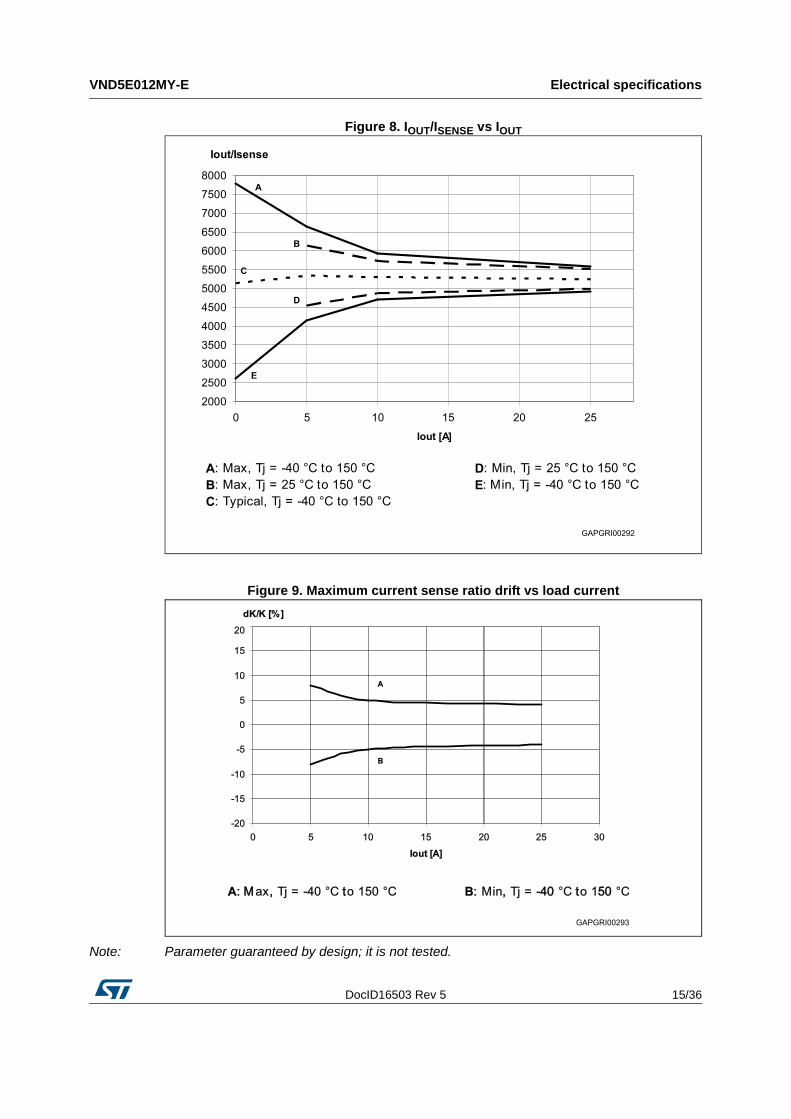
Figure 8. IOUT/ISENSE vs IOUT
Figure 9. Maximum current sense ratio drift vs load current
Note: Parameter guaranteed by design; it is not tested.
Electrical specifications VND5E012MY-E
16/36 DocID16503 Rev 5
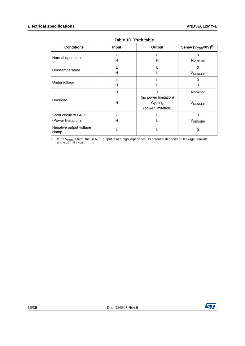
Table 10. Truth table
Conditions Input Output Sense (VCSD=0V)(1)
1. If the VCSD is high, the SENSE output is at a high impedance, its potential depends on leakage currents and external circuit.
Normal operationLH
LH
0Nominal
OvertemperatureLH
LL
0VSENSEH
UndervoltageLH
LL
00
Overload
H
H
X(no power limitation)
Cycling
(power limitation)
Nominal
VSENSEH
Short circuit to GND
(Power limitation)
L
H
L
L
0
VSENSEH
Negative output voltage clamp
L L 0

DocID16503 Rev 5 17/36
VND5E012MY-E Electrical specifications
35
Table 11. Electrical transient requirements (part 1)
ISO 7637-2: 2004(E)
Test pulse
Test levels(1)
1. The above test levels must be considered referred to VCC = 13.5 V except for pulse 5b.
Number of pulses or test times
Burst cycle/pulse repetition time
Delays andimpedanceIII IV
1 -75 V -100 V5000
pulses0.5 s 5 s 2 ms, 10 Ω
2a +37 V +50 V5000
pulses0.2 s 5 s 50 µs, 2 Ω
3a -100 V -150 V 1h 90 ms 100 ms 0.1 µs, 50 Ω
3b +75 V +100 V 1h 90 ms 100 ms 0.1 µs, 50 Ω
4 -6 V -7 V 1 pulse 100 ms, 0.01 Ω
5b(2)
2. Valid in case of external load dump clamp: 40V maximum referred to ground. The protection strategy allows PowerMOS to be cyclically switched on during load dump, so distributing the load dump energy along the time and to transfer a part of it to the load.
+65 V +87 V 1 pulse 400 ms, 2 Ω
Table 12. Electrical transient requirements (part 2)
ISO 7637-2: 2004(E)
Test pulse
Test level results(1)
1. The above test levels must be considered referred to VCC = 13.5 V except for pulse 5b
III IV
1 C C
2a C C
3a C C
3b C C
4 C C
5b(2)(3)
2. Valid in case of external load dump clamp: 40V maximum referred to ground. The protection strategy allows PowerMOS to be cyclically switched on during load dump, so distributing the load dump energy along the time and to transfer a part of it to the load.
3. Suppressed load dump (pulse 5b) is withstood with a minimum load connected as specified in Table 3: Absolute maximum rating.
C C
Table 13. Electrical transient requirements (part 3)
Class Contents
C All functions of the device are performed as designed after exposure to disturbance.
EOne or more functions of the device are not performed as designed after exposure to disturbance and cannot be returned to proper operation without replacing the device.

Electrical specifications VND5E012MY-E
18/36 DocID16503 Rev 5
2.4 Waveforms
Figure 10. Normal operation
Figure 11. Overload or short to GND
DocID16503 Rev 5 19/36
VND5E012MY-E Electrical specifications
35
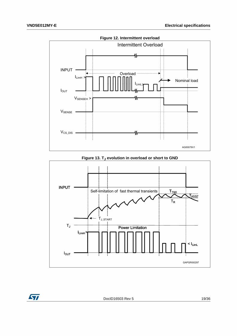
Figure 12. Intermittent overload
Figure 13. TJ evolution in overload or short to GND
Electrical specifications VND5E012MY-E
20/36 DocID16503 Rev 5
2.5 Electrical characteristics curves
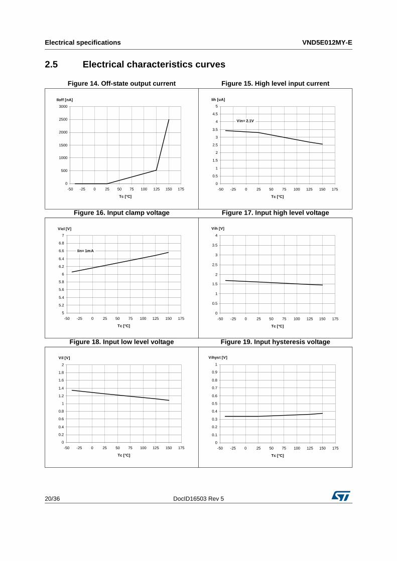
Figure 14. Off-state output current Figure 15. High level input current
Figure 16. Input clamp voltage Figure 17. Input high level voltage
Figure 18. Input low level voltage Figure 19. Input hysteresis voltage
Iloff [nA]
0
500
1000
1500
2000
2500
3000
-50 -25 0 25 50 75 100 125 150 175
Tc [°C]
Iih [uA]
0
0.5
1
1.5
2
2.5
3
3.5
4
4.5
5
-50 -25 0 25 50 75 100 125 150 175
Tc [°C]
Vin= 2.1V
Vicl [V]
5
5.2
5.4
5.6
5.8
6
6.2
6.4
6.6
6.8
7
-50 -25 0 25 50 75 100 125 150 175
Tc [°C]
Iin= 1mA
Vih [V]
0
0.5
1
1.5
2
2.5
3
3.5
4
-50 -25 0 25 50 75 100 125 150 175
Tc [°C]
Vil [V]
0
0.2
0.4
0.6
0.8
1
1.2
1.4
1.6
1.8
2
-50 -25 0 25 50 75 100 125 150 175
Tc [°C]
Vihyst [V]
0
0.1
0.2
0.3
0.4
0.5
0.6
0.7
0.8
0.9
1
-50 -25 0 25 50 75 100 125 150 175
Tc [°C]
DocID16503 Rev 5 21/36
VND5E012MY-E Electrical specifications
35
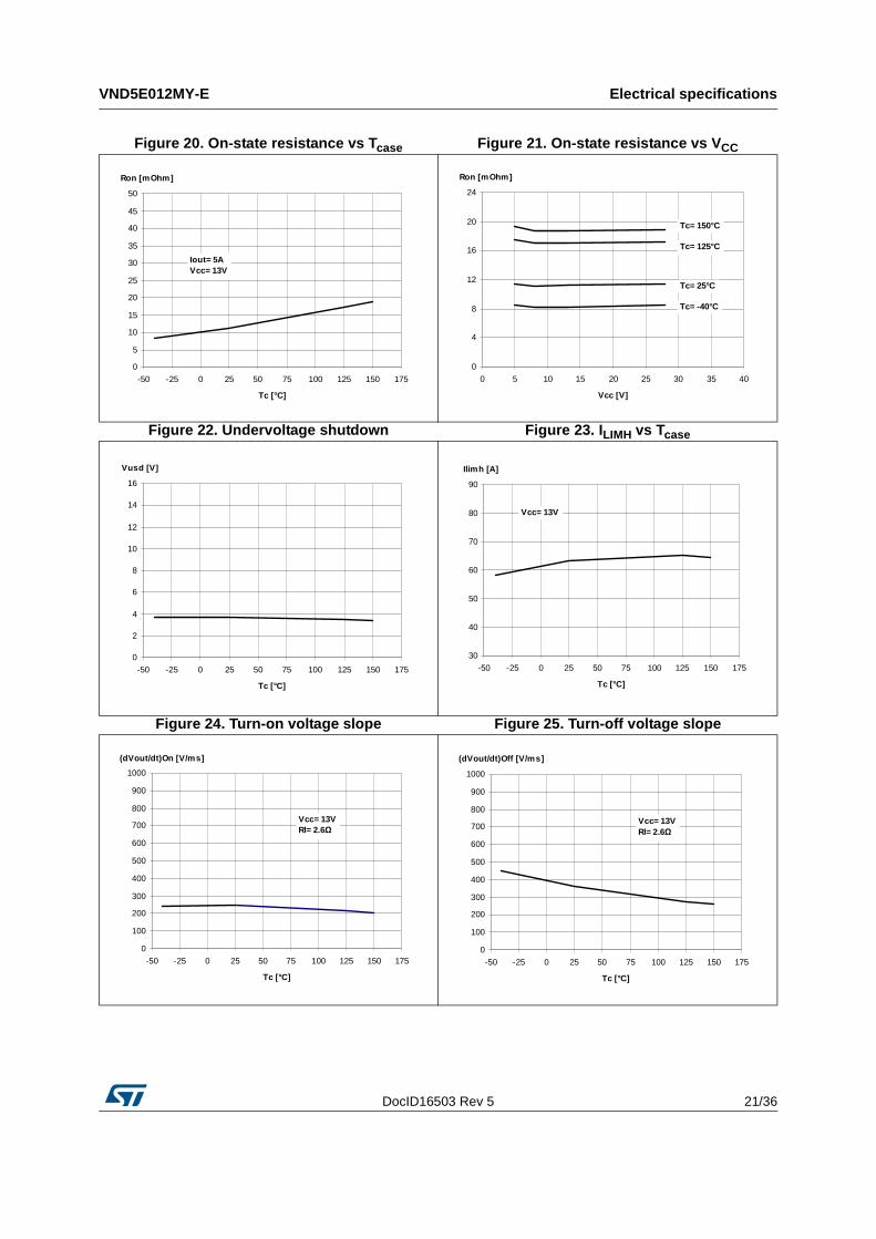
Figure 20. On-state resistance vs Tcase Figure 21. On-state resistance vs VCC
Figure 22. Undervoltage shutdown Figure 23. ILIMH vs Tcase
Figure 24. Turn-on voltage slope Figure 25. Turn-off voltage slope
Ron [mOhm]
0
5
10
15
20
25
30
35
40
45
50
-50 -25 0 25 50 75 100 125 150 175
Tc [°C]
Iout= 5AVcc= 13V
Ron [mOhm]
0
4
8
12
16
20
24
0 5 10 15 20 25 30 35 40
Vcc [V]
Tc= -40°C
Tc= 25°C
Tc= 125°C
Tc= 150°C
Vusd [V]
0
2
4
6
8
10
12
14
16
-50 -25 0 25 50 75 100 125 150 175
Tc [°C]
Ilimh [A]
30
40
50
60
70
80
90
-50 -25 0 25 50 75 100 125 150 175
Tc [°C]
Vcc= 13V
(dVout/dt)On [V/ms]
0
100
200
300
400
500
600
700
800
900
1000
-50 -25 0 25 50 75 100 125 150 175
Tc [°C]
Vcc= 13VRl= 2.6Ω
(dVout/dt)Off [V/ms]
0
100
200
300
400
500
600
700
800
900
1000
-50 -25 0 25 50 75 100 125 150 175
Tc [°C]
Vcc= 13VRl= 2.6Ω
Electrical specifications VND5E012MY-E
22/36 DocID16503 Rev 5
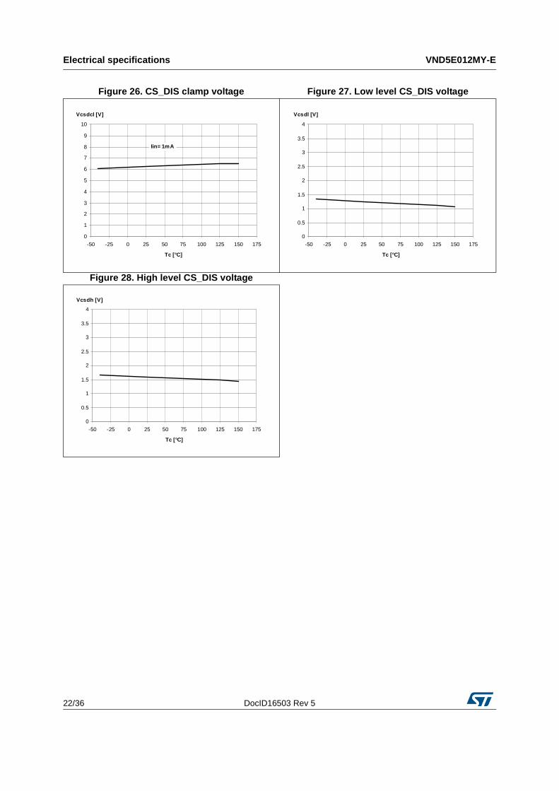
Figure 26. CS_DIS clamp voltage Figure 27. Low level CS_DIS voltage
Figure 28. High level CS_DIS voltage
Vcsdcl [V]
0
1
2
3
4
5
6
7
8
9
10
-50 -25 0 25 50 75 100 125 150 175
Tc [°C]
Iin= 1mA
Vcsdl [V]
0
0.5
1
1.5
2
2.5
3
3.5
4
-50 -25 0 25 50 75 100 125 150 175
Tc [°C]
Vcsdh [V]
0
0.5
1
1.5
2
2.5
3
3.5
4
-50 -25 0 25 50 75 100 125 150 175
Tc [°C]

DocID16503 Rev 5 23/36
VND5E012MY-E Application information
35
3 Application information
Figure 29. Application schematic
Note: Channel 2 has the same internal circuit as channel 1.
3.1 Load dump protection Dld is necessary (Voltage Transient Suppressor) if the load dump peak voltage exceeds the VCCPK max rating. The same applies if the device is subject to transients on the VCC line that are greater than the ones shown in the ISO 7637-2: 2004(E) table.
3.2 MCU I/Os protectionWhen negative transients are present on the VCC line, the control pin is pulled negative to approximately -1.5 V. ST suggests to insert a resistor (Rprot) in line to prevent the microcontroller I/Os pins from latching-up.
The value of these resistors is a compromise between the leakage current of microcontroller and the current required by the HSD I/Os (input levels compatibility) with the latch-up limit of microcontroller I/Os.
Equation 1
Calculation example:
For VCCpeak = - 1.5 V; Ilatchup ≥ 20 mA; VOHμC ≥ 4.5 V
75 Ω ≤ Rprot ≤ 240 kΩ.
vccpeak llatchup⁄ Rprot VOHμC VIH–( )≤ lIHmax⁄≤

Application information VND5E012MY-E
24/36 DocID16503 Rev 5
Recommended values: Rprot =10 kΩ, CEXT =10 nF.
3.3 Current sense and diagnosticThe current sense pin performs a double function (see Figure 30: Current sense and diagnostic):
• Current mirror of the load current in normal operation, delivering a current proportional to the load one according to a know ratio KX. The current ISENSE can be easily converted to a voltage VSENSE by means of an external resistor RSENSE. Linearity between IOUT and VSENSE is ensured up to 5V minimum (see parameter VSENSE in Table 9: Current sense (8V<VCC<18V)). The current sense accuracy depends on the output current (refer to current sense electrical characteristics Table 9: Current sense (8V<VCC<18V)).
• Diagnostic flag in fault conditions, delivering a fixed voltage VSENSEH up to a maximum current ISENSEH in case of the following fault conditions (refer to Truth table):
– Power limitation activation
– Overtemperature
A logic level high on CS_DIS pin sets at the same time all the current sense pins of the device in a high impedance state, thus disabling the current monitoring and diagnostic detection. This feature allows multiplexing of the microcontroller analog inputs by sharing of sense resistance and ADC line among different devices.
Figure 30. Current sense and diagnostic
Main MOSn41V
OUTn
RSENSE
RPROT
To uC ADC
Pwr_Lim
VSENSE
Overtemperature
CURRENT SENSEn
IOUT/KX
ISENSEH
VBAT
VSENSEH
Load
VCC
GND
CS_DIS

DocID16503 Rev 5 25/36
VND5E012MY-E Application information
35
3.4 Maximum demagnetization energy (VCC = 13.5V)
Figure 31. Maximum turn-off current versus inductance
Note: Values are generated with RL = 0 Ω.In case of repetitive pulses, Tjstart (at beginning of each demagnetization) of every pulse must not exceed the temperature specified above for curves A and B.
C: Tjstart = 125°C repetitive pulse
A: Tjstart = 150°C single pulse
B: Tjstart = 100°C repetitive pulse
1
10
100
1 10 100L (mH)
I (A
)
VNx5E012 - Single Pulse
Repetitive pulse Tjstart=100°C
Repetitive pulse Tjstart=125°C

Package and PCB thermal data VND5E012MY-E
26/36 DocID16503 Rev 5
4 Package and PCB thermal data
4.1 PowerSSO-36 thermal data
Figure 32. PowerSSO-36 PC board
Note: Layout condition of Rth and Zth measurements (PCB: Double layer, Thermal Vias, FR4 area= 129mm x 60mm, PCB thickness=1.6mm, Cu thickness=70μm (front and back side), Copper areas: from minimum pad lay-out to 8 cm2).

DocID16503 Rev 5 27/36
VND5E012MY-E Package and PCB thermal data
35
Figure 33. Rthj-amb vs PCB copper area in open box free air condition (one channel ON)
Figure 34. PowerSSO-36 thermal impedance junction ambient single pulse (one channel ON)

Package and PCB thermal data VND5E012MY-E
28/36 DocID16503 Rev 5
Figure 35. Thermal fitting model of a double channel HSD in PowerSSO-36(1)
1. The fitting model is a simplified thermal tool and is valid for transient evolutions where the embedded protections (power limitation or thermal cycling during thermal shutdown) are not triggered.
Equation 2: pulse calculation formula
Table 14. Thermal parameter
Area/island (cm2) Footprint 2 8
R1 (°C/W) 0.1
R2 (°C/W) 0.3
R3 (°C/W) 5
R4 (°C/W) 8
R5 (°C/W) 18 10 10
R6 (°C/W) 27 23 14
R7 (°C/W) 0.1
R8 (°C/W) 0.3
C1 (W.s/°C) 0.0025
C2 (W.s/°C) 0.005
C3 (W.s/°C) 0.04
C4 (W.s/°C) 0.5
C5 (W.s/°C) 1 2 2
C6 (W.s/°C) 3 6 9
ZTHδ RTH δ ZTHtp 1 δ–( )+⋅=
where δ tp T⁄=

DocID16503 Rev 5 29/36
VND5E012MY-E Package and PCB thermal data
35
C7 (W.s/°C) 0.0025
C8 (W.s/°C) 0.005
Table 14. Thermal parameter
Area/island (cm2) Footprint 2 8

Package information VND5E012MY-E
30/36 DocID16503 Rev 5
5 Package information
5.1 ECOPACK® packageIn order to meet environmental requirements, ST offers these devices in different grades of ECOPACK® packages, depending on their level of environmental compliance. ECOPACK® specifications, grade definitions and product status are available at: www.st.com. ECOPACK® is an ST trademark.

DocID16503 Rev 5 31/36
VND5E012MY-E Package information
35
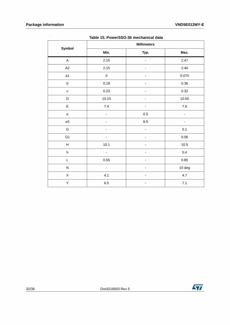
5.2 PowerSSO-36 mechanical data
Figure 36. PowerSSO-36 package dimensions
Package information VND5E012MY-E
32/36 DocID16503 Rev 5
l
Table 15. PowerSSO-36 mechanical data
SymbolMillimeters
Min. Typ. Max.
A 2.15 - 2.47
A2 2.15 - 2.40
a1 0 - 0.075
b 0.18 - 0.36
c 0.23 - 0.32
D 10.10 - 10.50
E 7.4 - 7.6
e - 0.5 -
e3 - 8.5 -
G - - 0.1
G1 - - 0.06
H 10.1 - 10.5
h - - 0.4
L 0.55 - 0.85
N - - 10 deg
X 4.1 - 4.7
Y 6.5 - 7.1
DocID16503 Rev 5 33/36
VND5E012MY-E Package information
35
5.3 Packing information
Figure 37. PowerSSO-36 tube shipment (no suffix)
Figure 38. PowerSSO-36 tape and reel shipment (suffix “TR”)
All dimensions are in mm.
Base Q.ty 49Bulk Q.ty 1225Tube length (± 0.5) 532A 3.5B 13.8C (± 0.1) 0.6
Base Q.ty 1000
Bulk Q.ty 1000A (max) 330B (min) 1.5
C (± 0.2) 13F 20.2G (+ 2 / -0) 24.4
N (min) 100T (max) 30.4
REEL DIMENSIONS
TAPE DIMENSIONSAccording to Electronic Industries Association(EIA) Standard 481 rev. A, Feb 1986
All dimensions are in mm.
Tape width W 24Tape Hole Spacing P0 (± 0.1) 4
Component Spacing P 12Hole Diameter D (± 0.05) 1.55Hole Diameter D1 (min) 1.5
Hole Position F (± 0.1) 11.5Compartment Depth K (max) 2.85Hole Spacing P1 (± 0.1) 2
Top
cover
tape
End
Start
No componentsNo components Components
500mm min
500mm minEmpty components pocketssaled with cover tape.
User direction of feed
Order codes VND5E012MY-E
34/36 DocID16503 Rev 5
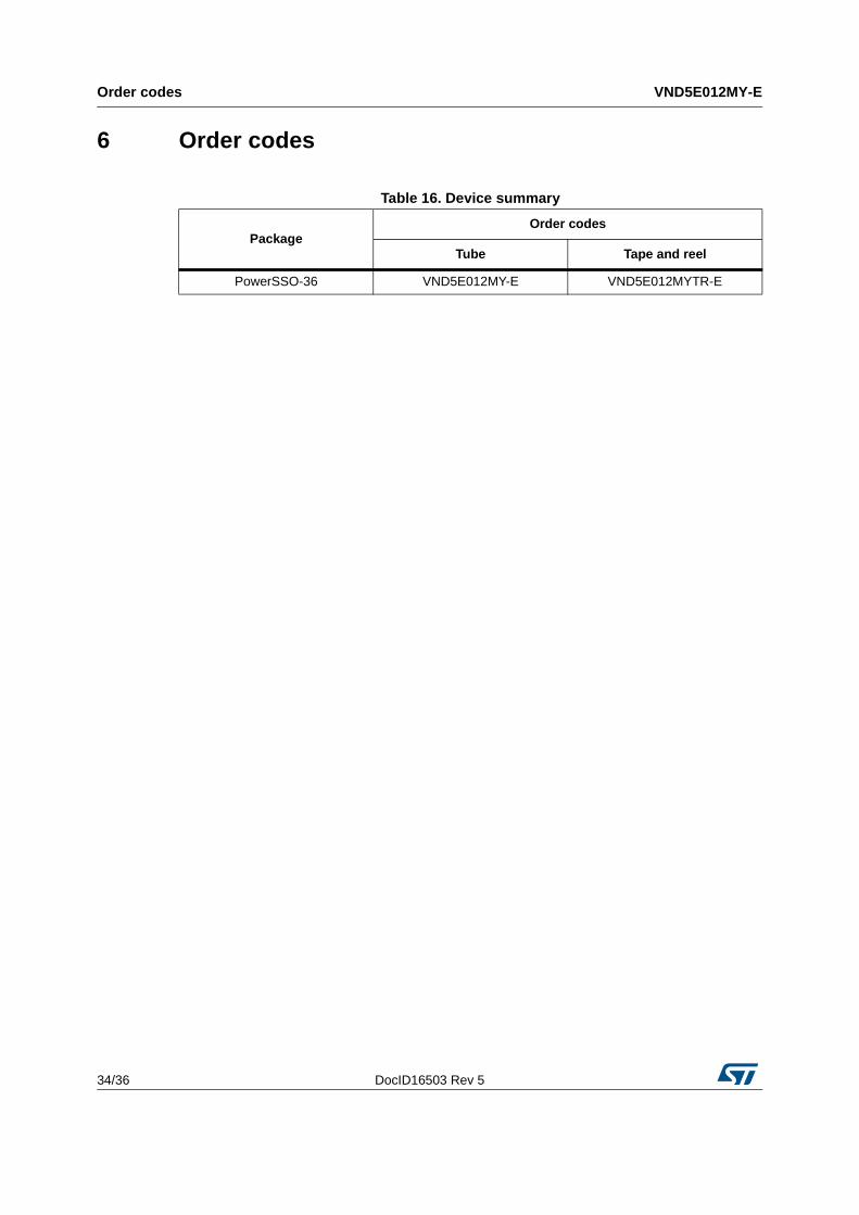
6 Order codes
Table 16. Device summary
PackageOrder codes
Tube Tape and reel
PowerSSO-36 VND5E012MY-E VND5E012MYTR-E
DocID16503 Rev 5 35/36
VND5E012MY-E Revision history
35
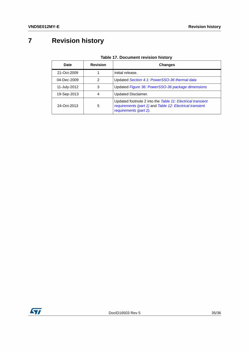
7 Revision history
Table 17. Document revision history
Date Revision Changes
21-Oct-2009 1 Initial release.
04-Dec-2009 2 Updated Section 4.1: PowerSSO-36 thermal data
11-July-2012 3 Updated Figure 36: PowerSSO-36 package dimensions
19-Sep-2013 4 Updated Disclaimer.
24-Oct-2013 5Updated footnote 2 into the Table 11: Electrical transient requirements (part 1) and Table 12: Electrical transient requirements (part 2).

VND5E012MY-E
36/36 DocID16503 Rev 5
Please Read Carefully:
Information in this document is provided solely in connection with ST products. STMicroelectronics NV and its subsidiaries (“ST”) reserve the right to make changes, corrections, modifications or improvements, to this document, and the products and services described herein at any time, without notice.
All ST products are sold pursuant to ST’s terms and conditions of sale.
Purchasers are solely responsible for the choice, selection and use of the ST products and services described herein, and ST assumes no liability whatsoever relating to the choice, selection or use of the ST products and services described herein.
No license, express or implied, by estoppel or otherwise, to any intellectual property rights is granted under this document. If any part of this document refers to any third party products or services it shall not be deemed a license grant by ST for the use of such third party products or services, or any intellectual property contained therein or considered as a warranty covering the use in any manner whatsoever of such third party products or services or any intellectual property contained therein.
UNLESS OTHERWISE SET FORTH IN ST’S TERMS AND CONDITIONS OF SALE ST DISCLAIMS ANY EXPRESS OR IMPLIED WARRANTY WITH RESPECT TO THE USE AND/OR SALE OF ST PRODUCTS INCLUDING WITHOUT LIMITATION IMPLIED WARRANTIES OF MERCHANTABILITY, FITNESS FOR A PARTICULAR PURPOSE (AND THEIR EQUIVALENTS UNDER THE LAWS OF ANY JURISDICTION), OR INFRINGEMENT OF ANY PATENT, COPYRIGHT OR OTHER INTELLECTUAL PROPERTY RIGHT.
ST PRODUCTS ARE NOT DESIGNED OR AUTHORIZED FOR USE IN: (A) SAFETY CRITICAL APPLICATIONS SUCH AS LIFE SUPPORTING, ACTIVE IMPLANTED DEVICES OR SYSTEMS WITH PRODUCT FUNCTIONAL SAFETY REQUIREMENTS; (B) AERONAUTIC APPLICATIONS; (C) AUTOMOTIVE APPLICATIONS OR ENVIRONMENTS, AND/OR (D) AEROSPACE APPLICATIONS OR ENVIRONMENTS. WHERE ST PRODUCTS ARE NOT DESIGNED FOR SUCH USE, THE PURCHASER SHALL USE PRODUCTS AT PURCHASER’S SOLE RISK, EVEN IF ST HAS BEEN INFORMED IN WRITING OF SUCH USAGE, UNLESS A PRODUCT IS EXPRESSLY DESIGNATED BY ST AS BEING INTENDED FOR “AUTOMOTIVE, AUTOMOTIVE SAFETY OR MEDICAL” INDUSTRY DOMAINS ACCORDING TO ST PRODUCT DESIGN SPECIFICATIONS. PRODUCTS FORMALLY ESCC, QML OR JAN QUALIFIED ARE DEEMED SUITABLE FOR USE IN AEROSPACE BY THE CORRESPONDING GOVERNMENTAL AGENCY.
Resale of ST products with provisions different from the statements and/or technical features set forth in this document shall immediately void any warranty granted by ST for the ST product or service described herein and shall not create or extend in any manner whatsoever, any liability of ST.
ST and the ST logo are trademarks or registered trademarks of ST in various countries.Information in this document supersedes and replaces all information previously supplied.
The ST logo is a registered trademark of STMicroelectronics. All other names are the property of their respective owners.
© 2013 STMicroelectronics - All rights reserved
STMicroelectronics group of companies
Australia - Belgium - Brazil - Canada - China - Czech Republic - Finland - France - Germany - Hong Kong - India - Israel - Italy - Japan - Malaysia - Malta - Morocco - Philippines - Singapore - Spain - Sweden - Switzerland - United Kingdom - United States of America
www.st.com
Related Documents