DEVELOPMENT OF A GSM BASED VEHICLE MONITORING & SECURITY SYSTEM Chapter 1 1. Introduction 1.1 Aim The main aim of this project is to provide security to the vehicles. The system automatically locks the vehicle as soon as it receives a predefined message from the user. 1.2 Features • The controlling unit contains the microcontroller and the GSM modem interfaced to it. The controlling unit will be fixed to the vehicle. • The microcontroller continuously checks whether it has received any message from the modem. • The modem provides the communication interface. The GSM modem is a wireless modem that works with a GSM wireless network • Whenever anyone tries to unlock or take away the vehicle, immediately a message will be sent to the user mobile. • The user, after checking the message, can respond immediately to save his vehicle. • The microcontroller retrieves this message from the modem by issuing certain AT and T commands to the modem. • Thus, after receiving the message from the modem, the microcontroller automatically locks the vehicle. • This will be done perfectly without the involvement of any human. 1.3 Applications

Welcome message from author
This document is posted to help you gain knowledge. Please leave a comment to let me know what you think about it! Share it to your friends and learn new things together.
Transcript

DEVELOPMENT OF A GSM BASED VEHICLE MONITORING & SECURITY SYSTEM
Chapter 1
1. Introduction
1.1 Aim
The main aim of this project is to provide security to the vehicles. The system automatically locks the vehicle as soon as it receives a predefined message from the user.
1.2 Features
• The controlling unit contains the microcontroller and the GSM modem interfaced to it. The controlling unit will be fixed to the vehicle.
• The microcontroller continuously checks whether it has received any message from the modem.
• The modem provides the communication interface. The GSM modem is a wireless modem that works with a GSM wireless network
• Whenever anyone tries to unlock or take away the vehicle, immediately a message will be sent to the user mobile.
• The user, after checking the message, can respond immediately to save his vehicle.
• The microcontroller retrieves this message from the modem by issuing certain AT and T commands to the modem.
• Thus, after receiving the message from the modem, the microcontroller automatically locks the vehicle.
• This will be done perfectly without the involvement of any human.
1.3 Applications
using GPS tracking system we can detect the vehicle any where in the global
automatic reduction of vehicle speed where an obstacle on the way to present loss in an accident
diction of aichohol for a driver and limit the speed of the vechile not more than 40km/hr
The GSM Modem supports popular "AT" command set so that users can develop
applications quickly
Uses GSM technology for following applications:
1. Access control devices: Access control devices can communicate with
servers and security staff through SMS messaging. Complete log of
transaction is available at the head-office Server instantly without any
wiring involved and device can instantly alert security personnel on their

mobile phone in case of any problem
2. Transaction terminals: EDC (Electronic Data Capturing) machines can
use SMS messaging to confirm transactions from central servers. The
main benefit is that central server can be anywhere in the world
3. Supply Chain Management: With a central server in your head office
with GSM capability, you can receive instant transaction data from all
your branch offices, warehouses and business associates with nil
downtime and low cost.
Limitations
The control kit should be placed inside the vehicle far away from the temperature
Care should be taken such that all components in the control kit must be in
condition
Must and should specify the predefined messages in the source program
The gsm frequencys must be considered
literature survey
THE 8051 MICROCONTROLLER AND EMBEDDED SYSTEMS
-Muhammad ali mazidi -janice gillispie mazidi
THE 8051 MICROCONTROLLER ARCHITECTURE,PROGRAMING AND APPLICATIONS
-Kenneth j.Ayala -Ramesh s.gaonkar
ELECTRONIC COMPONENTS -D.V.Prasad
INTRDUCTION TO GSM -Lawrence Harte
1.4 Organization of the Thesis
In view of the proposed thesis work explanation of theoretical aspects and
algorithms used in this work are presented as per the sequence described below.
Chapter 1 describes a brief review of introduction of the project.

Chapter 2 discusses the theoretical chapters of project.
Chapter 3 describes the hardware design considerations.
Chapter 4 explains about software implementations.
Chapter 5 describes about application implementation.
Chapter 6 gives results and conclusions
Chapter 2
Theoretical chapter
Embedded Systems:
An embedded system can be defined as a computing device that does a specific focused
job. Appliances such as the air-conditioner, VCD player, DVD player, printer, fax
machine, mobile phone etc. are examples of embedded systems. Each of these appliances
will have a processor and special hardware to meet the specific requirement of the
application along with the embedded software that is executed by the processor for
meeting that specific requirement. The embedded software is also called “firm ware”.
The desktop/laptop computer is a general purpose computer. You can use it for a variety
of applications such as playing games, word processing, accounting, software
development and so on. In contrast, the software in the embedded systems is always fixed
listed below:
· Embedded systems do a very specific task, they cannot be programmed to do different
things. Embedded systems have very limited resources, particularly the memory.
Generally, they do not have secondary storage devices such as the CDROM or the
floppy disk. Embedded systems have to work against some deadlines. A specific job has
to be completed within a specific time. In some embedded systems, called real-time
systems, the deadlines are stringent. Missing a deadline may cause a catastrophe-loss of
life or damage to property. Embedded systems are constrained for power. As many
embedded systems operate through a battery, the power consumption has to be very
low.
· Some embedded systems have to operate in extreme environmental conditions such as
very high temperatures and humidity.

Following are the advantages of Embedded Systems:
1. They are designed to do a specific task and have real time performance
constraints which must be met.
2. They allow the system hardware to be simplified so costs are reduced.
3. They are usually in the form of small computerized parts in larger devices which
serve a general purpose.
4. The program instructions for embedded systems run with limited computer
hardware resources, little memory and small or even non-existent keyboard or
screen.
The Evolution of Mobile Telephone Systems
Cellular is one of the fastest growing and most demanding telecommunications
applications. Today, it represents a continuously increasing percentage of all new
telephone subscriptions around the world. Currently there are more than 45 million
cellular subscribers worldwide, and nearly 50 percent of those subscribers are located in
the United States.
The concept of cellular service is the use of low power transmitters where frequencies
can be reused within a geographic area. The idea of cell based mobile radio service was
formulated in the United States at Bell Labs in the early 1970s. Cellular systems began in
the United States with the release of the advanced mobile phone service (AMPS) system
in 1983. The AMPS standard was adopted by Asia, Latin America and Oceanic countries,
creating the largest potential market in the world for cellular.
In the early 1980s, most mobile telephone systems were analog rather than digital, like
today's newer systems. One challenge facing analog systems was the inability to handle
the growing capacity needs in a cost efficient manner. As a result, digital technology was
welcomed.
The advantages of digital systems over analog systems include ease of signaling, lower
levels of interference, integration of transmission and switching and increased ability to

meet capacity demands. The table below shows the worldwide development of mobile
telephone systems.
The implementation of the project design can be divided in two parts.
Hardware implementation
Firmware implementation
Hardware implementation deals in drawing the schematic on the plane paper according to
the application, testing the schematic design over the breadboard using the various IC’s to
find if the design meets the objective, carrying out the PCB layout of the schematic tested
on breadboard, finally preparing the board and testing the designed hardware.
The firmware part deals in programming the microcontroller so that it can control the
operation of the IC’s used in the implementation. In the present work, we have used the
Orcad design software for PCB circuit design, the Keil µv3 software development tool to
write and compile the source code, which has been written in the C language. The
Proload programmer has been used to write this compile code into the microcontroller.
The firmware implementation is explained in the next chapter.

The project design and principle are explained in this chapter using the block diagram
and circuit diagram. The block diagram discusses about the required components of the
design and working condition is explained using circuit diagram and system wiring
diagram.
Microcontrollers:
Microprocessors and microcontrollers are widely used in embedded systems products.
Microcontroller is a programmable device. A microcontroller has a CPU in addition to a
fixed amount of RAM, ROM, I/O ports and a timer embedded all on a single chip. The
fixed amount of on-chip ROM, RAM and number of I/O ports in microcontrollers makes
them ideal for many applications in which cost and space are critical.
The Intel 8051 is Harvard architecture, single chip microcontroller (µC) which was
developed by Intel in 1980 for use in embedded systems. It was popular in the 1980s and
early 1990s, but today it has largely been superseded by a vast range of enhanced devices
with 8051-compatible processor cores that are manufactured by more than 20
independent manufacturers including Atmel, Infineon Technologies and Maxim
Integrated Products.
8051 is an 8-bit processor, meaning that the CPU can work on only 8 bits of data at a
time. Data larger than 8 bits has to be broken into 8-bit pieces to be processed by the
CPU. 8051 is available in different memory types such as UV-EPROM, Flash and NV-
RAM.
Features of AT89S52:

8K Bytes of Re-programmable Flash Memory.
RAM is 256 bytes.
4.0V to 5.5V Operating Range.
Fully Static Operation: 0 Hz to 33 MHz’s
Three-level Program Memory Lock.
256 x 8-bit Internal RAM.
32 Programmable I/O Lines.
Three 16-bit Timer/Counters.
Eight Interrupt Sources.
Full Duplex UART Serial Channel.
Low-power Idle and Power-down Modes.
Interrupt recovery from power down mode.
Watchdog timer.
Dual data pointer.
Power-off flag.
Fast programming time.
Flexible ISP programming (byte and page mode).
Description:
The AT89s52 is a low-voltage, high-performance CMOS 8-bit microcomputer with 8K
bytes of Flash programmable memory. The device is manufactured using Atmel’s high
density nonvolatile memory technology and is compatible with the industry-standard
MCS-51 instruction set. The on chip flash allows the program memory to be
reprogrammed in system or by a conventional non volatile memory programmer. By
combining a versatile 8-bit CPU with Flash on a monolithic chip, the Atmel AT89s52 is a
powerful microcomputer, which provides a highly flexible and cost-effective solution to
many embedded control applications.
In addition, the AT89s52 is designed with static logic for operation down to zero
frequency and supports two software selectable power saving modes. The Idle Mode
stops the CPU while allowing the RAM, timer/counters, serial port and interrupt system

to continue the functioning. The power-down mode saves the RAM contents but freezes
the oscillator disabling all other chip functions until the next hardware reset.
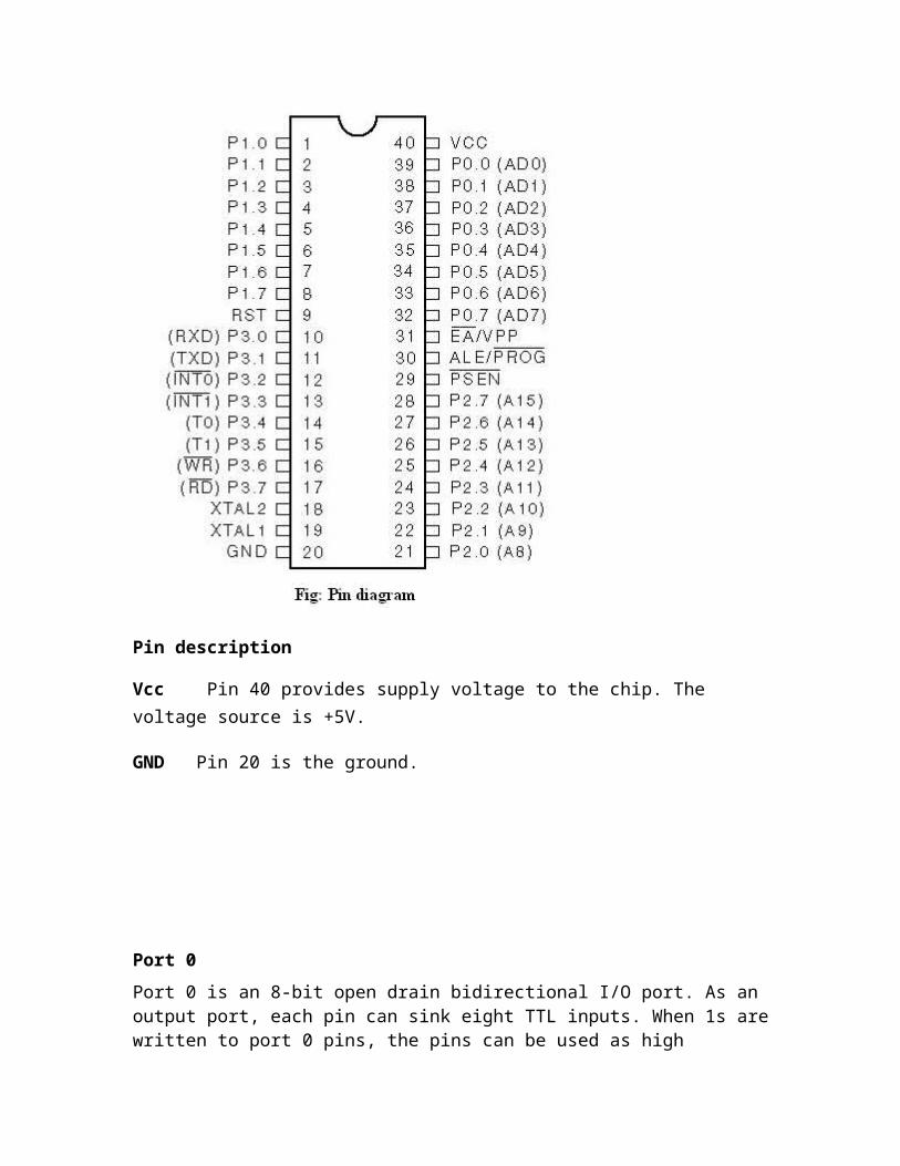
Pin description
Vcc Pin 40 provides supply voltage to the chip. The voltage source is +5V.
GND Pin 20 is the ground.
Port 0
Port 0 is an 8-bit open drain bidirectional I/O port. As an output port, each pin can sink eight TTL inputs. When 1s are written to port 0 pins, the pins can be used as high impedance inputs. Port 0 can also be configured to be the multiplexed low-order

address/data bus during accesses to external program and data memory. In this mode, P0
has internal pull-ups.
Port 0 also receives the code bytes during Flash programming and outputs the code bytes
during Program verification. External pull-ups are required during program verification
Port 1
Port 1 is an 8-bit bidirectional I/O port with internal pull-ups. The Port 1 output buffers
can sink/source four TTL inputs. When 1s are written to Port 1 pins, they are pulled high
by the internal pull-ups and can be used as inputs. As inputs, Port 1 pins that are
externally being pulled low will source current (IIL) because of the internal pull-ups. In
addition, P1.0 and P1.1 can be configured to be the timer/counter 2 external count input
(P1.0/T2) and the timer/counter 2 trigger input (P1.1/T2EX), respectively, as shown in
the following table.
Port 1 also receives the low-order address bytes during Flash programming and
verification.
Port 2
Port 2 is an 8-bit bidirectional I/O port with internal pull-ups. The Port 2 output buffers
can sink/source four TTL inputs. When 1s are written to Port 2 pins, they are pulled high
by the internal pull-ups and can be used as inputs. As inputs, Port 2 pins that are
externally being pulled low will source current (IIL) because of the internal pull-ups.
Port 2 emits the high-order address byte during fetches from external program memory
and during accesses to external data memory that uses 16-bit addresses (MOVX @
DPTR). In this application, Port 2 uses strong internal pull-ups when emitting 1s. During

accesses to external data memory that uses 8-bit addresses (MOVX @ RI), Port 2 emits
the contents of the P2 Special Function Register. The port also receives the high-order
address bits and some control signals during Flash programming and verification.
Port 3
Port 3 is an 8-bit bidirectional I/O port with internal pull-ups. The Port 3 output buffers can sink/source four TTL inputs. When 1s are written to Port 3 pins, they are pulled high by the internal pull-ups and can be used as inputs. As inputs, Port 3 pins that are externally being pulled low will source current (IIL) because of the pull-ups. Port 3 receives some control signals for Flash programming and verification.
Port 3 also serves the functions of various special features of the AT89S52, as shown in
the following table.
RST
Reset input A high on this pin for two machine cycles while the oscillator is running
resets the device. This pin drives high for 98 oscillator periods after the Watchdog times
out. The DISRTO bit in SFR AUXR (address 8EH) can be used to disable this feature. In
the default state of bit DISRTO, the RESET HIGH out feature is enabled.
ALE/PROG
Address Latch Enable (ALE) is an output pulse for latching the low byte of the address
during accesses to external memory. This pin is also the program pulse input (PROG)
during Flash programming.

In normal operation, ALE is emitted at a constant rate of 1/6 the oscillator frequency and
may be used for external timing or clocking purposes. Note, however, that one ALE pulse
is skipped during each access to external data memory.
If desired, ALE operation can be disabled by setting bit 0 of SFR location 8EH. With the
bit set, ALE is active only during a MOVX or MOVC instruction. Otherwise, the pin is
weakly pulled high. Setting the ALE-disable bit has no effect if the microcontroller is in
external execution mode.
PSEN
Program Store Enable (PSEN) is the read strobe to external program memory. When
the AT89S52 is executing code from external program memory, PSEN is activated twice
each machine cycle, except that two PSEN activations are skipped during each access to
external data memory.
EA/VPP
External Access Enable EA must be strapped to GND in order to enable the device to
fetch code from external program memory locations starting at 0000H up to FFFFH.
Note, however, that if lock bit 1 is programmed, EA will be internally latched on reset.
EA should be strapped to VCC for internal program executions. This pin also receives the
12-volt programming enable voltage (VPP) during Flash programming.
XTAL1
Input to the inverting oscillator amplifier and input to the internal clock operating circuit.
XTAL2
Output from the inverting oscillator amplifier.
XTAL1 and XTAL2 are the input and output, respectively, of an inverting amplifier that
can be configured for use as an on-chip oscillator. Either a quartz crystal or ceramic
resonator may be used. To drive the device from an external clock source, XTAL2 should
be left unconnected while XTAL1 is driven. There are no requirements on the duty cycle
of the external clock signal, since the input to the internal clocking circuitry is through a
divide-by-two flip-flop, but minimum and maximum voltage high and low time
specifications must be observed.
UART
The Atmel 8051 Microcontrollers implement three general purpose, 16-bit timers/
counters. They are identified as Timer 0, Timer 1 and Timer 2 and can be independently
configured to operate in a variety of modes as a timer or as an event counter. When
operating as a timer, the timer/counter runs for a programmed length of time and then
issues an interrupt request. When operating as a counter, the timer/counter counts

negative transitions on an external pin. After a preset number of counts, the counter
issues an interrupt request. The various operating modes of each timer/counter are
described in the following sections.
A basic operation consists of timer registers THx and TLx (x= 0, 1) connected in cascade
to form a 16-bit timer. Setting the run control bit (TRx) in TCON register turns the timer
on by allowing the selected input to increment TLx. When TLx overflows it increments
THx; when THx overflows it sets the timer overflow flag (TFx) in TCON register.
Setting the TRx does not clear the THx and TLx timer registers. Timer registers can be
accessed to obtain the current count or to enter preset values. They can be read at any
time but TRx bit must be cleared to preset their values, otherwise the behavior of the
timer/counter is unpredictable.
The C/T control bit (in TCON register) selects timer operation or counter operation, by
selecting the divided-down peripheral clock or external pin Tx as the source for the
counted signal. TRx bit must be cleared when changing the mode of operation, otherwise
the behavior of the timer/counter is unpredictable. For timer operation (C/Tx# = 0), the
timer register counts the divided-down peripheral clock. The timer register is incremented
once every peripheral cycle (6 peripheral clock periods). The timer clock rate is FPER /
6, i.e. FOSC / 12 mode. There are no restrictions on the duty cycle of the external input
signal, but to ensure that a given level is sampled at least once before it changes, it should
be held for at least one full peripheral cycle. In addition to the “timer” or “counter”
selection, Timer 0 and Timer 1 have four operating modes from which to select which are
selected by bit-pairs (M1, M0) in TMOD. Modes 0, 1and 2 are the same for both
timer/counters. Mode 3 is different.
The four operating modes are described below. Timer 2, has three modes of operation:
‘capture’, ‘auto-reload’ and ‘baud rate generator’.
in standard mode or FOSC / 6 in X2 mode. For counter operation (C/Tx# = 1), the timer
register counts the negative transitions on the Tx external input pin. The external input is
sampled every peripheral cycle. When the sample is high in one cycle and low in the next
one, the counter is incremented.

GSM Technology:
Definition of GSM:
GSM (Global System for Mobile communications) is an open, digital cellular technology
used for transmitting mobile voice and data services.
GSM (Global System for Mobile communication) is a digital mobile telephone system
that is widely used in Europe and other parts of the world. GSM uses a variation of Time
Division Multiple Access (TDMA) and is the most widely used of the three digital
wireless telephone technologies (TDMA, GSM, and CDMA).
GSM digitizes and compresses data, then sends it down a channel with two other streams
of user data, each in its own time slot. It operates at either the 900 MHz or 1,800 MHz
frequency band. It supports voice calls and data transfer speeds of up to 9.6 kbit/s,
together with the transmission of SMS (Short Message Service).
Since it takes 2 cycles (12 peripheral clock periods) to recognize a negative transition, the
maximum count rate is FPER / 12, i.e. FOSC / 24 in standard mode or FOSC / 12 in X2
History
In 1982, the European Conference of Postal and Telecommunications Administrations
(CEPT) created the Group Special Mobile (GSM) to develop a standard for a mobile
telephone system that could be used across Europe. In 1987, a memorandum of
understanding was signed by 13 countries to develop a common cellular telephone
system across Europe. Finally the system created by SINTEF lead by Torleiv Maseng
was selected.
In 1989, GSM responsibility was transferred to the European Telecommunications
Standards Institute (ETSI) and phase I of the GSM specifications were published in 1990.
The first GSM network was launched in 1991 by Radiolinja in Finland with joint
technical infrastructure maintenance from Ericsson.

By the end of 1993, over a million subscribers were using GSM phone networks being
operated by 70 carriers across 48 countries. As of the end of 1997, GSM service was
available in more than 100 countries and has become the de facto standard in Europe and
Asia.
GSM Frequencies
GSM networks operate in a number of different frequency ranges (separated into GSM
frequency ranges for 2G and UMTS frequency bands for 3G). Most 2G GSM networks
operate in the 900 MHz or 1800 MHz bands. Some countries in the Americas (including
Canada and the United States) use the 850 MHz and 1900 MHz bands because the 900
and 1800 MHz frequency bands were already allocated. Most 3G GSM networks in
Europe operate in the 2100 MHz frequency band. The rarer 400 and 450 MHz frequency
bands are assigned in some countries where these frequencies were previously used for
first-generation systems.
GSM-900 uses 890–915 MHz to send information from the mobile station to the base
station (uplink) and 935–960 MHz for the other direction (downlink), providing 124 RF
channels (channel numbers 1 to 124) spaced at 200 kHz. Duplex spacing of 45 MHz is
used. In some countries the GSM-900 band has been extended to cover a larger frequency
range. This 'extended GSM', E-GSM, uses 880–915 MHz (uplink) and 925–960 MHz
(downlink), adding 50 channels (channel numbers 975 to 1023 and 0) to the original
GSM-900 band.
Time division multiplexing is used to allow eight full-rate or sixteen half-rate speech
channels per radio frequency channel. There are eight radio timeslots (giving eight burst
periods) grouped into what is called a TDMA frame. Half rate channels use alternate
frames in the same timeslot. The channel data rate for all 8 channels is 270.833 Kbit/s,
and the frame duration is 4.615 ms.
The transmission power in the handset is limited to a maximum of 2 watts in
GSM850/900 and 1 watt in GSM1800/1900. GSM operates in the 900MHz and 1.8GHz
bands in Europe and the 1.9GHz and 850MHz bands in the US. The 850MHz band is also
used for GSM and 3G in Australia, Canada and many South American countries. By
having harmonized spectrum across most of the globe, GSM’s international roaming
capability allows users to access the same services when travelling abroad as at home.
This gives consumers seamless and same number connectivity in more than 218
countries.
Terrestrial GSM networks now cover more than 80% of the world’s population. GSM
satellite roaming has also extended service access to areas where terrestrial coverage is
not available.
Mobile Telephony Standards
Standard Generation Frequency band Throughput
GSM 2GAllows transfer of voice or low-volume digital data. 9.6 kbps
9.6 kbps
GPRS 2.5GAllows transfer of voice or moderate-volume digital data.
21.4-171.2 kbps
48 kbps
EDGE 2.75GAllows simultaneous transfer of voice and digital data.
43.2-345.6 kbps
171 kbps
UMTS 3GAllows simultaneous transfer of voice and high-speed digital data. 0.144-2 Mbps
384 kbps
1G
The first generation of mobile telephony (written 1G) operated using analogue
communications and portable devices that were relatively large. It used primarily the
following standards:
AMPS (Advanced Mobile Phone System), which appeared in 1976 in the United
States, was the first cellular network standard. It was used primarily in the
Americas, Russia and Asia. This first-generation analogue network had weak
security mechanisms which allowed hacking of telephones lines.
TACS (Total Access Communication System) is the European version of the
AMPS model. Using the 900 MHz frequency band, this system was largely used
in England and then in Asia (Hong-Kong and Japan).

ETACS (Extended Total Access Communication System) is an improved version
of the TACS standard developed in the United Kingdom that uses a larger number
of communication channels.
The first-generation cellular networks were made obsolete by the appearance of an
entirely digital second generation.
Second Generation of Mobile Networks (2G)
The second generation of mobile networks marked a break with the first generation of
cellular telephones by switching from analogue to digital. The main 2G mobile telephony
standards are:
GSM (Global System for Mobile communications) is the most commonly used
standard in Europe at the end of the 20th century and supported in the United
States. This standard uses the 900 MHz and 1800 MHz frequency bands in
Europe. In the United States, however, the frequency band used is the 1900 MHz
band. Portable telephones that are able to operate in Europe and the United States
are therefore called tri-band.
CDMA (Code Division Multiple Access) uses a spread spectrum technique that
allows a radio signal to be broadcast over a large frequency range.
TDMA (Time Division Multiple Access) uses a technique of time division of
communication channels to increase the volume of data transmitted
simultaneously. TDMA technology is primarily used on the American continent,
in New Zealand and in the Asia-Pacific region.
With the 2G networks, it is possible to transmit voice and low volume digital data, for
example text messages (SMS, for Short Message Service) or multimedia messages
(MMS, for Multimedia Message Service). The GSM standard allows a maximum data
rate of 9.6 kbps.

Extensions have been made to the GSM standard to improve throughput. One of these is
the GPRS (General Packet Radio System) service which allows theoretical data rates on
the order of 114 Kbit/s but with throughput closer to 40 Kbit/s in practice. As this
technology does not fit within the "3G" category, it is often referred to as 2.5G
The EDGE (Enhanced Data Rates for Global Evolution) standard, billed as 2.75G,
quadruples the throughput improvements of GPRS with its theoretical data rate of 384
Kbps, thereby allowing the access for multimedia applications. In reality, the EDGE
standard allows maximum theoretical data rates of 473 Kbit/s, but it has been limited in
order to comply with the IMT-2000 (International Mobile Telecommunications-2000)
specifications from the ITU (International Telecommunications Union).
3G
The IMT-2000 (International Mobile Telecommunications for the year 2000)
specifications from the International Telecommunications Union (ITU) defined the
characteristics of 3G (third generation of mobile telephony). The most important of these
characteristics are:
1. High transmission data rate.
2. 144 Kbps with total coverage for mobile use3. 384 Kbps with medium coverage for pedestrian use.
4. 2 Mbps with reduced coverage area for stationary use.
5. World compatibility.
6. Compatibility of 3rd generation mobile services with second generation networks.
3G offers data rates of more than 144 Kbit/s, thereby allowing the access to multimedia
uses such as video transmission, video-conferencing or high-speed internet access. 3G
networks use different frequency bands than the previous networks: 1885-2025 MHz and
2110-2200 MHz.
The main 3G standard used in Europe is called UMTS (Universal Mobile
Telecommunications System) and uses WCDMA (Wideband Code Division Multiple
Access) encoding. UMTS technology uses 5 MHz bands for transferring voice and data,
with data rates that can range from 384 Kbps to 2 Mbps. HSDPA (High Speed Downlink
Packet Access) is a third generation mobile telephony protocol, (considered as "3.5G"),
which is able to reach data rates on the order of 8 to 10 Mbps. HSDPA technology uses
the 5 GHz frequency band and uses WCDMA encoding.
Introduction to the GSM Standard
The GSM (Global System for Mobile communications) network is at the start of the
21st century, the most commonly used mobile telephony standard in Europe. It is called as
Second Generation (2G) standard because communications occur in an entirely digital
mode, unlike the first generation of portable telephones.
When it was first standardized in 1982, it was called as Group Special Mobile and later,
it became an international standard called "Global System for Mobile
communications" in 1991.
In Europe, the GSM standard uses the 900 MHz and 1800 MHz frequency bands. In the
United States, however, the frequency band used is the 1900 MHz band. For this reason,
portable telephones that are able to operate in both Europe and the United States are
called tri-band while those that operate only in Europe are called bi-band.
The GSM standard allows a maximum throughput of 9.6 kbps which allows transmission
of voice and low-volume digital data like text messages (SMS, for Short Message
Service) or multimedia messages (MMS, for Multimedia Message Service).
GSM Standards:
GSM uses narrowband TDMA, which allows eight simultaneous calls on the same radio
frequency.
There are three basic principles in multiple access, FDMA (Frequency Division Multiple
Access), TDMA (Time Division Multiple Access), and CDMA (Code Division Multiple

Access). All three principles allow multiple users to share the same physical channel. But
the two competing technologies differ in the way user sharing the common resource.
TDMA allows the users to share the same frequency channel by dividing the signal into
different time slots. Each user takes turn in a round robin fashion for transmitting and
receiving over the channel. Here, users can only transmit in their respective time slot.
CDMA uses a spread spectrum technology that is it spreads the information contained in
a particular signal of interest over a much greater bandwidth than the original signal.
Unlike TDMA, in CDMA several users can transmit over the channel at the same time.
TDMA in brief:
In late1980’s, as a search to convert the existing analog network to digital as a means to
improve capacity, the cellular telecommunications industry association chose TDMA
over FDMA.
Time Division Multiplex Access is a type of multiplexing where two or more channels of
information are transmitted over the same link by allocating a different time interval for
the transmission of each channel. The most complex implementation using TDMA
principle is of GSM’s (Global System for Mobile communication). To reduce the effect
of co-channel interference, fading and multipath, the GSM technology can use frequency
hoping, where a call jumps from one channel to another channel in a short interval.

TDMA systems still rely on switch to determine when to perform a handoff. Handoff
occurs when a call is switched from one cell site to another while travelling. The TDMA
handset constantly monitors the signals coming from other sites and reports it to the
switch without caller’s awareness. The switch then uses this information for making
better choices for handoff at appropriate times. TDMA handset performs hard handoff,
i.e., whenever the user moves from one site to another, it breaks the connection and then
provides a new connection with the new site.
Advantages of TDMA:
There are lots of advantages of TDMA in cellular technologies.
1. It can easily adapt to transmission of data as well as voice communication.
2. It has an ability to carry 64 kbps to 120 Mbps of data rates. This allows the
operator to do services like fax, voice band data and SMS as well as bandwidth
intensive application such as multimedia and video conferencing.
3. Since TDMA technology separates users according to time, it ensures that there
will be no interference from simultaneous transmissions.
4. It provides users with an extended battery life, since it transmits only portion of
the time during conversations. Since the cell size grows smaller, it proves to save
base station equipment, space and maintenance.

TDMA is the most cost effective technology to convert an analog system to digital.
Disadvantages of TDMA:
One major disadvantage using TDMA technology is that the users has a predefined time
slot. When moving from one cell site to other, if all the time slots in this cell are full the
user might be disconnected. Likewise, if all the time slots in the cell in which the user is
currently in are already occupied, the user will not receive a dial tone.
The second problem in TDMA is that it is subjected to multipath distortion. To overcome
this distortion, a time limit can be used on the system. Once the time limit is expired, the
signal is ignored.
The concept of cellular network
Mobile telephone networks are based on the concept of cells, circular zones that overlap
to cover a geographical area.
Cellular networks are based on the use of a central transmitter-receiver in each cell,
called a "base station" (or Base Transceiver Station, written BTS). The smaller the
radius of a cell, the higher is the available bandwidth. So, in highly populated urban
areas, there are cells with a radius of a few hundred meters, while huge cells of up to 30
kilometers provide coverage in rural areas.
In a cellular network, each cell is surrounded by 6 neighbouring cells (thus a cell is
generally drawn as a hexagon). To avoid interference, adjacent cells cannot use the same
frequency. In practice, two cells using the same frequency range must be separated by a
distance of two to three times the diameter of the cell.
Architecture of the GSM Network
In a GSM network, the user terminal is called a mobile station. A mobile station is made
up of a SIM (Subscriber Identity Module) card allowing the user to be uniquely identified
and a mobile terminal.
The terminals (devices) are identified by a unique 15-digit identification number
called IMEI (International Mobile Equipment Identity). Each SIM card also has a unique
(and secret) identification number called IMSI (International Mobile Subscriber
Identity). This code can be protected using a 4-digit key called a PIN code.
The SIM card therefore allows each user to be identified independently of the terminal
used during communication with a base station. Communications occur through a radio
link (air interface) between a mobile station and a base station.
All the base stations of a cellular network are connected to a base station
controller (BSC) which is responsible for managing distribution of the resources. The
system consisting of the base station controller and its connected base stations is called
the Base Station Subsystem (BSS).
Finally, the base station controllers are themselves physically connected to the Mobile
Switching Centre (MSC), managed by the telephone network operator, which connects
them to the public telephone network and the Internet. The MSC belongs to a Network
Station Subsystem (NSS), which is responsible for managing user identities, their
location and establishment of communications with other subscribers. The MSC is
generally connected to databases that provide additional functions:
1. The Home Location Register (HLR) is a database containing information
(geographic position, administrative information etc.) of the subscribers registered
in the area of the switch (MSC).
2. The Visitor Location Register (VLR) is a database containing information of
users other than the local subscribers. The VLR retrieves the data of a new user
from the HLR of the user's subscriber zone. The data is maintained as long as the
user is in the zone and is deleted when the user leaves or after a long period of
inactivity (terminal off).
3. The Equipment Identify Register (EIR) is a database listing the mobile
terminals.
4. The Authentication Centre (AUC) is responsible for verifying user identities.
5. The cellular network formed in this way is designed to support mobility via
management of handovers (movements from one cell to another).
Finally, GSM networks support the concept of roaming i.e., movement from one
operator network to another.
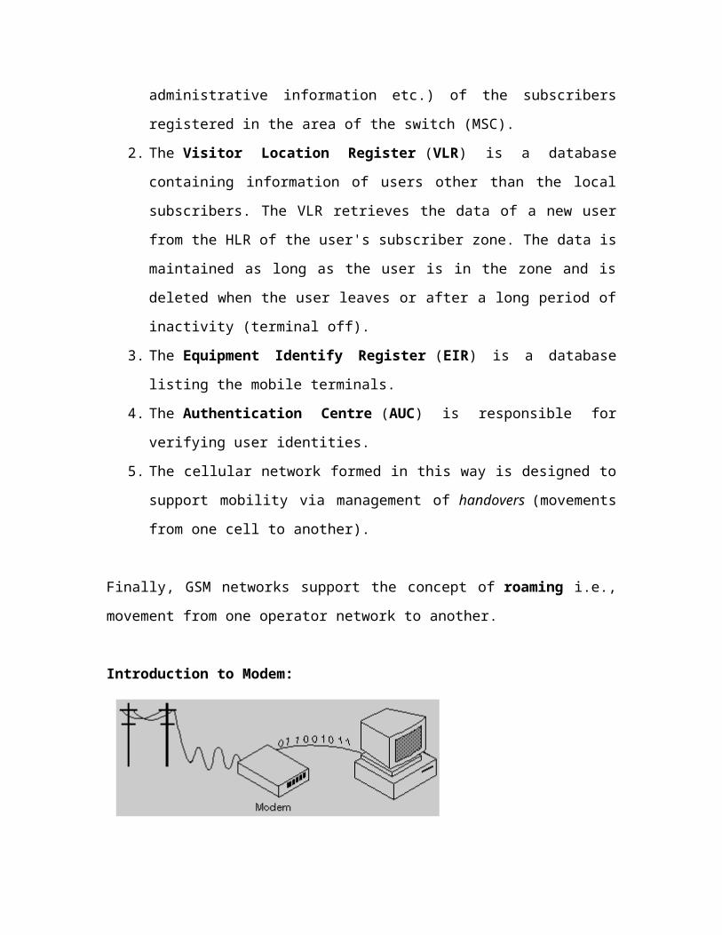
Introduction to Modem:
Modem stands for modulator-demodulator.
A modem is a device or program that enables a computer to transmit data over telephone
or cable lines. Computer information is stored digitally, whereas information transmitted
over telephone lines is transmitted in the form of analog waves. A modem converts
between these two forms.

Fortunately, there is one standard interface for connecting external modems to computers
called RS-232. Consequently, any external modem can be attached to any computer that
has an RS-232 port, which almost all personal computers have. There are also modems
that come as an expansion board that can be inserted into a vacant expansion slot. These
are sometimes called onboard or internal modems.
While the modem interfaces are standardized, a number of different protocols for
formatting data to be transmitted over telephone lines exist. Some, like CCITT V.34 are
official standards, while others have been developed by private companies. Most modems
have built-in support for the more common protocols at slow data transmission speeds at
least, most modems can communicate with each other. At high transmission speeds,
however, the protocols are less standardized.
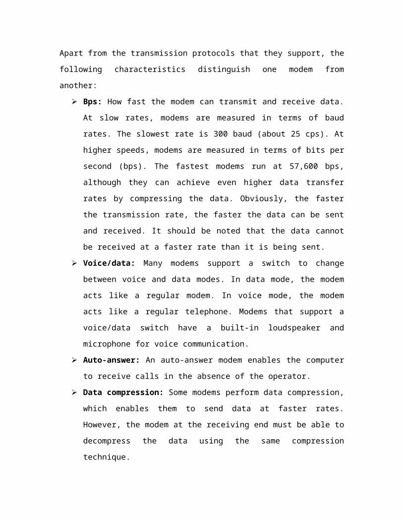
Apart from the transmission protocols that they support, the following characteristics
distinguish one modem from another:
Bps: How fast the modem can transmit and receive data. At slow rates, modems
are measured in terms of baud rates. The slowest rate is 300 baud (about 25 cps).
At higher speeds, modems are measured in terms of bits per second (bps). The
fastest modems run at 57,600 bps, although they can achieve even higher data
transfer rates by compressing the data. Obviously, the faster the transmission rate,
the faster the data can be sent and received. It should be noted that the data cannot
be received at a faster rate than it is being sent.
Voice/data: Many modems support a switch to change between voice and data
modes. In data mode, the modem acts like a regular modem. In voice mode, the
modem acts like a regular telephone. Modems that support a voice/data switch
have a built-in loudspeaker and microphone for voice communication.
Auto-answer: An auto-answer modem enables the computer to receive calls in
the absence of the operator.
Data compression: Some modems perform data compression, which enables
them to send data at faster rates. However, the modem at the receiving end must
be able to decompress the data using the same compression technique.

Flash memory: Some modems come with flash memory rather than conventional
ROM which means that the communications protocols can be easily updated if
necessary.
Fax capability: Most modern modems are fax modems, which mean that they
can send and receive faxes.
GSM Modem:
A GSM modem is a wireless modem that works with a GSM wireless network. A
wireless modem behaves like a dial-up modem. The main difference between them is that
a dial-up modem sends and receives data through a fixed telephone line while a wireless
modem sends and receives data through radio waves.
A GSM modem can be an external device or a PC Card / PCMCIA Card. Typically, an
external GSM modem is connected to a computer through a serial cable or a USB cable.
A GSM modem in the form of a PC Card / PCMCIA Card is designed for use with a
laptop computer. It should be inserted into one of the PC Card / PCMCIA Card slots of a
laptop computer.
Like a GSM mobile phone, a GSM modem requires a SIM card from a wireless carrier in
order to operate.
A SIM card contains the following information:
Subscriber telephone number (MSISDN)
International subscriber number (IMSI, International Mobile Subscriber Identity)
State of the SIM card
Service code (operator)
Authentication key
PIN (Personal Identification Code)
PUK (Personal Unlock Code)
Computers use AT commands to control modems. Both GSM modems and dial-up
modems support a common set of standard AT commands. In addition to the standard AT
commands, GSM modems support an extended set of AT commands. These extended AT
commands are defined in the GSM standards. With the extended AT commands, the
following operations can be performed:
Reading, writing and deleting SMS messages.
Sending SMS messages.
Monitoring the signal strength.
Monitoring the charging status and charge level of the battery.
Reading, writing and searching phone book entries.
Chapter 3 Hardware design considerations3.1 Introduction Hardware design deals in drawing the schematic on the plane paper according
to the application, testing the schematic design over the breadboard using the various IC’s
to find if the design meets the objective, carrying out the PCB layout of the schematic
tested on breadboard, finally preparing the board and testing the designed hardware.
The project design and principle are explained in this chapter using the block
diagram and circuit diagram. The block diagram discusses about the required components

of the design and working condition is explained using circuit diagram and system wiring
diagram.
3.2 components used
Fig: Block diagram for the project design The components used are
1. power supply2. max 2323. sensors 4. crystal circuit5. reset circuit6. lcd display7. buzzer8. gsm modem9. ignition switch10. micro controller
3.3 power supply The input to the circuit is applied from the regulated power supply. The a.c. input
i.e., 230V from the mains supply is step down by the transformer to 12V and is fed to a
rectifier. The output obtained from the rectifier is a pulsating d.c voltage. So in order to
get a pure d.c voltage, the output voltage from the rectifier is fed to a filter to remove any
a.c components present even after rectification. Now, this voltage is given to a voltage
regulator to obtain a pure constant dc voltage.
Transformer:
Usually, DC voltages are required to operate various electronic equipment and
these voltages are 5V, 9V or 12V. But these voltages cannot be obtained directly. Thus
the a.c input available at the mains supply i.e., 230V is to be brought down to the
required voltage level. This is done by a transformer. Thus, a step down transformer is
employed to decrease the voltage to a required level.
Rectifier:
The output from the transformer is fed to the rectifier. It converts A.C. into
pulsating D.C. The rectifier may be a half wave or a full wave rectifier. In this project, a
bridge rectifier is used because of its merits like good stability and full wave rectification.
Filter:

Capacitive filter is used in this project. It removes the ripples from the output of
rectifier and smoothens the D.C. Output received from this filter is constant until the
mains voltage and load is maintained constant. However, if either of the two is varied,
D.C. voltage received at this point changes. Therefore a regulator is applied at the output
stage.
Voltage regulator:
As the name itself implies, it regulates the input applied to it. A voltage regulator
is an electrical regulator designed to automatically maintain a constant voltage level. In
this project, power supply of 5V and 12V are required. In order to obtain these voltage
levels, 7805 and 7812 voltage regulators are to be used. The first number 78 represents
positive supply and the numbers 05, 12 represent the required output voltage levels.
3.4 Max 232
Max232 IC is a specialized circuit which makes standard voltages as required by
RS232 standards. This IC provides best noise rejection and very reliable against
discharges and short circuits. MAX232 IC chips are commonly referred to as line drivers.
To ensure data transfer between PC and microcontroller, the baud rate and voltage levels
of Microcontroller and PC should be the same. The voltage levels of microcontroller are
logic1 and logic 0 i.e., logic 1 is +5V and logic 0 is 0V. But for PC, RS232 voltage levels
are considered and they are: logic 1 is taken as -3V to -25V and logic 0 as +3V to +25V.
So, in order to equal these voltage levels, MAX232 IC is used. Thus this IC converts
RS232 voltage levels to microcontroller voltage levels and vice versa.
RS232 CABLE:
To allow compatibility among data communication equipment, an interfacing standard called RS232 is used. Since the standard was set long before the advent of the TTL logic family, its input and output voltage levels are not TTL compatible. For this reason, to connect any RS232 to a microcontroller system, voltage converters such as MAX232 are used to convert the TTL logic levels to the RS232 voltage levels and vice versa3.5 Sensors
The sensors used in this project are Heartbeat and Temperature sensor. The
Heartbeat sensor used is basically a LED and LDR arrangement.
3.5.1 LED and LDR arrangement
The Heartbeat sensor used in this project is basically a LED and LDR arrangement. The
LED used in this arrangement is a high intensity LED.
Heart beat is sensed by using a high intensity type LED and LDR. The finger is placed
between the LED and LDR. As sensor, a photo diode or a photo transistor can be used.
The skin may be illuminated with visible (red) using transmitted or reflected light for
detection. The very small changes in reflectivity or in transmittance caused by the
varying blood content of human tissue are almost invisible. Various noise sources may
produce disturbance signals with amplitudes equal or even higher than the amplitude of

the pulse signal. Valid pulse measurement therefore requires extensive preprocessing of
the raw signal.
The setup described here uses a red LED for transmitted light illumination and a LDR as
detector. With only slight changes in the preamplifier circuit the same hardware and
software could be used with other illumination and detection concepts.
3.5.2 Precision Centigrade Temperature Sensor
LM35 converts temperature value into electrical signals. LM35 series sensors are
precision integrated-circuit temperature sensors whose output voltage is linearly
proportional to the Celsius temperature. The LM35 requires no external calibration since
it is internally calibrated. . The LM35 does not require any external calibration or
trimming to provide typical accuracies of ±1⁄4°C at room temperature and ±3⁄4°C over a
full −55 to +150°C temperature range.
The LM35’s low output impedance, linear output, and precise inherent calibration make
interfacing to readout or control circuitry especially easy. It can be used with single
power supplies, or with plus and minus supplies. As it draws only 60 μA from its supply,
it has very low self-heating, less than 0.1°C in still air.
Features
Calibrated directly in ° Celsius (Centigrade)
Linear + 10.0 mV/°C scale factor
0.5°C accuracy guaranteed (at +25°C)

Rated for full −55° to +150°C range
Suitable for remote applications
Low cost due to wafer-level trimming
Operates from 4 to 30 volts
Less than 60 μA current drain
Low self-heating, 0.08°C in still air
Nonlinearity only ±1⁄4°C typical
Low impedance output, 0.1 W for 1 mA load
The characteristic of this LM35 sensor is:
For each degree of centigrade temperature it outputs 10milli volts.
The arrangement of this sensor in our board is as shown in the figure below.
In this we directly connect the output of the sensor to the base of the transistor as of
LM35 for every 1˚C rise of temperature the output will increase for 10mV. Now if the
temperature reaches 70˚C the output voltage will be 0.7V which is enough for the
transistor junction to be biased. Hence the transistor gets on and the output is sensed by
the microcontroller.
Operation:

The number of SMS messages that can be processed by a GSM modem per minute is
very low i.e., about 6 to 10 SMS messages per minute.
Chapter 4 Software implementation Introduction
The firmware part deals in programming the microcontroller so that it can control the operation of the IC’s used in the implementation. In the present work, we have used the Orcad design software for PCB circuit design, the Keil µv3 software development tool to write and compile the source code, which has been written in the C language. The Proload programmer has been used to write this compile code into the microcontroller
Algorithm
Serial Programming Algorithm To program and verify the AT89S52 in the serial programming mode, the following sequence is recommended: 1. Power-up sequence: Apply power between VCC and GND pins. Set RST pin to "H". If a crystal is not connected across pins XTAL1 and XTAL2, apply a 3 MHz to 33
MHz clock to XTAL1 pin and wait for at least 10 milliseconds. 2. Enable serial programming by sending the Programming Enable serial instruction to pin MOSI/P1.5. The frequency of the shift clock supplied at pin SCK/P1.7 needs to be less than the CPU clock at XTAL1 divided by 16. 3. The Code array is programmed one byte at a time by supplying the address and data together with the appropriate Write instruction. The write cycle is self timed and typically takes less than 1 ms at 5V. 4. Any memory location can be verified by using the Read instruction which returns the content at the selected address at serial output MISO/P1.6. 5. At the end of a programming session, RST can be set low to commence normal device operation
source code
4.3.1 C file
#include<reg51.h> #include"lcddisplay.h" #include"UART.h" #include"eeprom.h" #include<string.h>
sbit MOTOR = P2^4;sbit buz = P2^7;sbit sw = P2^5;
unsigned char mobilenum[];
void main(){ code unsigned char msg1[]="WELCOME",c1[]="at",c2[]="ate0"; bit l1=0,l2=0,control=0;
unsigned char GSMdata[43];
unsigned char numcnt;unsigned char a,b,count,ccount,status=0,jjj,i,b1; buz=0; MOTOR=0; sw=1; lcd_init(); UART_init(); lcdcmd(0x85); msgdisplay(msg1); delay(300);
a=read_eeprom(0); if(a==0xff) for(i=0;i<10;i++) { write_eeprom(i,mobilenum[i]); delay(200); } lcdcmd(0x01); msgdisplay("searching for"); lcdcmd(0xc0); msgdisplay("GSM modem"); delay(100); send_to_modem(c2); //to avoid echo signals, enter(); send_to_modem(c1); // TO CHECKING GSM MODEM... enter();
while(RI==0); // not. RI=0; lcdcmd(0x01); msgdisplay("SYSTEM CONNECTED"); send_to_modem("at+cmgf=1"); enter(); lcdcmd(0x01); msgdisplay(mobilenum); st: lcdcmd(0x01); msgdisplay("VEHICLE"); lcdcmd(0xC0); msgdisplay("SECURITY SYSTEM"); delay(500);
while(RI==1) { RI=0; delay(100); }
if(control) { send_to_modem("at+cmgs=");
ch_send_to_modem('"'); send_to_modem(mobilenum); ch_send_to_modem('"');
enter(); if(l1)
{ lcdcmd(0x01);
msgdisplay("vehicle stopped"); send_to_modem("vehicle stopped ");
} if(l2) { lcdcmd(0x01);
msgdisplay("vehicle on"); send_to_modem("vehicle on");
} control=l1=l2=0;
} while(1) { if((sw==0)&&(status==0))
{ buz=0; while(sw==0); MOTOR=1; lcdcmd(0x01); msgdisplay("vehicle on");
goto st;}if(RI==1) { RI=0; b=SBUF; while(RI==0);
b=SBUF; RI=0;
while(RI==0); b=SBUF;
RI=0; while(RI==0); b=SBUF;
RI=0; if(b=='C') {
while(RI==0); b=SBUF;
RI=0; if(b=='M') {
while(RI==0); b=SBUF;
RI=0; }
if(b=='T') {
while(RI==0); b=SBUF;
RI=0;

} if(b=='I')
{
lcdcmd(0x01); msgdisplay("NEW message ");
delay(100); b1=b; send_to_modem("at+cmgr="); ch_send_to_modem(b); enter(); count=0; jjj=0; a=0; ccount=0; numcnt=0; while(count!=3) { while(RI==0);
b=SBUF; if(b==',') { if(numcnt<15)
{ if(numcnt>4) mobilenum[numcnt-5]=b; a=1; numcnt++; }
else a=0;
} if(count==2) GSMdata[jjj++]=SBUF;
RI=0; if(b==10) count+=1; ccount+=1; } mobilenum[10]='\0'; lcdcmd(0x01);
send_to_modem("at+cmgd="); ch_send_to_modem(b1); enter(); msgdisplay("message reading"); delay(500); lcdcmd(0x01);
msgdisplay(gpsdata); lcdcmd(0xc0);
msgdisplay(mobilenum); delay(500);

if(!strcmp(gpsdata,"STOP")) { MOTOR=0; status=1; l1=1; control=1; buz=1; }
if(!strcmp(gpsdata,"123")) { MOTOR=1; status=0; l2=1; control=1; buz=0; }
}
goto st; } } }
4.3.2 UART
#include<reg51.h>void UART_init(void);void send_to_modem (unsigned char s[]);void enter (void);void ch_send_to_modem (unsigned char single_char);
void UART_init(void) { TMOD=0x20; TH1=0xFD; SCON=0x50; TR1=1; }
void send_to_modem (unsigned char s[])

{ unsigned char r;
for(r=0;s[r]!='\0';r++) // to send the command to GSM modem to avoid echo signal { // the command is "ate0", SBUF=s[r]; while(TI==0); TI=0; delay(100); } // enter(); }
void enter (void) { SBUF=13; // Enter ASC values are 13 and 10, while(TI==0); // After sending commands to GSM modem you must be send Enter's ASC values. TI=0; SBUF=10; while(TI==0); TI=0; }
void ch_send_to_modem (unsigned char single_char) {
TMOD=0x20; TH1=0xFd; SCON=0x50; TR1=1; SBUF=single_char; while(TI==0); TI=0; delay(10); }

Chapter 5 Application Implementation
5.1 Hardware implementation
5.2 software implementation Software Tools Required
Keil µv3, Proload are the two software tools used to program microcontroller.
The working of each software tool is explained below in detail.
Keil Compiler:
Keil compiler is software used where the machine language code is written and
compiled. After compilation, the machine source code is converted into hex code which

is to be dumped into the microcontroller for further processing. Keil compiler also
supports C language code.
Proload:
Proload is software which accepts only hex files. Once the machine code is
converted into hex code, that hex code has to be dumped into the microcontroller and this
is done by the Proload. Proload is a programmer which itself contains a microcontroller
in it other than the one which is to be programmed. This microcontroller has a program in
it written in such a way that it accepts the hex file from the Keil compiler and dumps this
hex file into the microcontroller which is to be programmed. As the Proload programmer

kit requires power supply to be operated, this power supply is given from the power
supply circuit designed above. It should be noted that this programmer kit contains a
power supply section in the board itself but in order to switch on that power supply, a
source is required. Thus this is accomplished from the power supply board with an output
of 12volts.
Features
Supports major Atmel 89 series devices
Auto Identify connected hardware and devices
Error checking and verification in-built
Lock of programs in chip supported to prevent program copying
20 and 40 pin ZIF socket on-board
Auto Erase before writing and Auto Verify after writing
Informative status bar and access to latest programmed file
Simple and Easy to use
Works on 57600 speed
Chapter 6
Results and Discussions
5.1 Results
Assemble the circuit on the PCB as shown in Fig 5.1. After assembling the circuit
on the PCB, check it for proper connections before switching on the power supply.

5.2 Conclusion
The implementation of GSM based Vehicle Security system is done successfully.
The communication is properly done without any interference between different modules
in the design. Design is done to meet all the specifications and requirements. Software
tools like Keil Uvision Simulator, Proload to dump the source code into the
microcontroller, Orcad Lite for the schematic diagram have been used to develop the
software code before realizing the hardware.
Continuously reading the output values from the sensors, check the values, if they
are triggered, alert the buzzer and also send the predefined message to the user mobile
through GSM modem is the main job carried out by the microcontroller. The mechanism
is controlled by the microcontroller.
Circuit is implemented in Orcad and implemented on the microcontroller board.
The performance has been verified both in software simulator and hardware design. The
total circuit is completely verified functionally and is following the application software.
It can be concluded that the design implemented in the present work provide portability,
flexibility and the data transmission is also done with low power consumption.
Working procedure:
GSM based vehicle security system is an Embedded system that provides security to the
vehicles using GSM technology.
The working of the project is as below:

Whenever the user wants to start his vehicle, he has to press the ignition switch. When
this switch is pressed, the microcontroller detects this and sends the predefined message
to the user mobile. Thus, the user can have the complete control of the vehicle in his
hand. If anyone other than the user or the driver presses the switch, the user receives the
message from the controlling unit and thus, the user can know that someone is trying to
take away the vehicle and can immediately send the predefined message to stop the
vehicle to the controlling unit.
After the user gets the message to his mobile, the user can now send the predefined message in the form of a password to start or stop the vehicle. The motor of the vehicle is operated when the controller receives the message from the user mobile
BIBLIOGRAPHY
THE 8051 MICROCONTROLLER AND EMBEDDED SYSTEMS
-Muhammad ali mazidi -janice gillispie mazidi
THE 8051 MICROCONTROLLER ARCHITECTURE,PROGRAMING AND APPLICATIONS
-Kenneth j.Ayala -Ramesh s.gaonkar
ELECTRONIC COMPONENTS -D.V.Prasad
INTRDUCTION TO GSM -Lawrence Harte
http://www.national.comhttp://www.atmel.comhttp://www.microsoftsearch.com
Related Documents