University of Ulster at Jordanstown University of Applied Sciences, Augsburg Master of Engineering VLSI Design Project Report Processor Implementation in VHDL According to Computer Organisation & Design by David A. Patterson and John L. Hennessy Author(s): M. Linder M. Schmid Supervisor(s): J. Färber A. Eder Submitted: 06/07/07

Welcome message from author
This document is posted to help you gain knowledge. Please leave a comment to let me know what you think about it! Share it to your friends and learn new things together.
Transcript

University of Ulster at JordanstownUniversity of Applied Sciences, Augsburg
Master of EngineeringVLSI Design Project Report
ProcessorImplementation
in VHDLAccording to Computer Organisation & Design
by David A. Patterson and John L. Hennessy
Author(s): M. LinderM. Schmid
Supervisor(s): J. FärberA. Eder
Submitted: 06/07/07

Document Revision History, Designers
Document Revision History
Rev. Date Author Description
0.1 15/05/2007 M. Schmid First draft release
0.2 15/05/2007 M. Linder Features of the project
0.3 29/05/2007 M. Linder Target Spec. (2.1, 2.2)
0.4 10/06/2007 M. Linder Target Spec. (2.3)
0.5 30/06/2007 M. Linder - include jump instruction to Target Spec.
- Module Spec. of Control
0.6 02/07/2007 M. Linder Module Spec. of Data
0.6.1 02/07/2007 M. Schmid Module Spec. of ALU and Memory
0.6.2 03/07/2007 M. Schmid Design Tasks
0.7 04/07/2007 M. Linder - Module Spec. of Datapath
- Synthesis Results
- References
0.8 05/07/2007 M. Linder, M. Schmid - Synthesis Results
- Source Code
- Conclusion
1.0 05/07/2007 M. Linder, M. Schmid Final release
Designer(s)
M. Linder [email protected]
M. Schmid [email protected]
Contact
Michael LinderAngerstraße 8a86356 Neusäß, GermanyPhone: +49 (0) 176 22 93 58 30Mail: [email protected]
Martin SchmidFichtenstraße 286500 Kutzenhausen, GermanyPhone: +49 (0) 160 92 94 91 54Mail: [email protected]
M. Linder, M. Schmid II
Department of Electrical Engineering

Contents
Contents
1 Introduction................................................................................ 11.1 Starting from a Simple Implementation Scheme...................................11.2 Using Multicycle Implementations.........................................................21.3 Enhancing Performance with Pipelining................................................2
2 Target Specification................................................................... 32.1 Building a Datapath...............................................................................3
2.1.1 Major Components.................................................................................... 32.1.2 Components for Arithmetic and Logic Functions....................................... 42.1.3 Load word (lw) and store word (sw) instructions........................................ 52.1.4 Branch on equal instruction....................................................................... 62.1.5 Jump Instruction........................................................................................ 6
2.2 Simple Implementation Scheme............................................................72.2.1 Creating a Single Datapath....................................................................... 72.2.2 ALU Control............................................................................................... 82.2.3 Main Control.............................................................................................. 92.2.4 Disadvantages of a Single-Cycle Implementation................................... 10
2.3 Multicycle Implementation...................................................................112.3.1 Additions and Changes in the Scheme.................................................... 112.3.2 Execution of Instructions in Clock Cycles................................................ 142.3.3 Defining the Control by a Finite State Machine........................................ 18
3 Design Tasks............................................................................ 21
4 Module Specification............................................................... 224.1 ALU......................................................................................................22
4.1.1 Functional Description............................................................................. 224.1.2 Block Diagram......................................................................................... 234.1.3 Simulation Results................................................................................... 264.1.4 Design Files............................................................................................. 26
4.2 Memory................................................................................................274.2.1 Functional Description............................................................................. 274.2.2 Block Diagram......................................................................................... 284.2.3 Simulation Results................................................................................... 284.2.4 Design Files............................................................................................. 29
M. Linder, M. Schmid III
Department of Electrical Engineering

Contents
4.3 Control..................................................................................................304.3.1 Functional Description............................................................................. 304.3.2 State Diagram......................................................................................... 314.3.3 Block Diagram......................................................................................... 324.3.4 Simulation Results................................................................................... 334.3.5 Design Files............................................................................................. 33
4.4 Data Path.............................................................................................344.4.1 Instruction Fetch...................................................................................... 34
4.4.1.1 Functional Description.................................................................................... 34
4.4.1.2 Block Diagram................................................................................................ 34
4.4.1.3 Design Files.................................................................................................... 35
4.4.2 Instruction Decode.................................................................................. 354.4.2.1 Functional Description.................................................................................... 35
4.4.2.2 Block Diagram................................................................................................ 35
4.4.2.3 Design Files.................................................................................................... 36
4.4.3 Execution................................................................................................. 364.4.3.1 Functional Description.................................................................................... 36
4.4.3.2 Block Diagram................................................................................................ 37
4.4.3.3 Design Files.................................................................................................... 38
4.4.4 Memory Writeback.................................................................................. 394.4.4.1 Functional Description.................................................................................... 39
4.4.4.2 Block Diagram................................................................................................ 40
4.4.4.3 Design Files.................................................................................................... 41
4.4.5 Data Path................................................................................................ 424.4.5.1 Block Diagram................................................................................................ 42
4.4.5.2 Design Files.................................................................................................... 42
4.5 Processor and Memroy........................................................................434.5.1 Functional Description............................................................................. 434.5.2 Block Diagram......................................................................................... 434.5.3 Design Files............................................................................................. 44
5 Synthesis Results.................................................................... 45
6 Results of Prototype Testing.................................................. 476.1 Description...........................................................................................476.2 Simulation Result.................................................................................49
7 Conclusion................................................................................ 507.1 Our own experiences...........................................................................50
M. Linder, M. Schmid IV
Department of Electrical Engineering

Contents
7.2 Annotations to “Computer Organization & Design” [PaHe98].............507.3 Further work on the project..................................................................51
8 Appendix................................................................................... 528.1 Design files..........................................................................................52
8.1.1 Project Entities........................................................................................ 528.1.2 Project Architectures............................................................................... 588.1.3 Package.................................................................................................. 798.1.4 Testbenches............................................................................................ 80
8.2 References...........................................................................................91
M. Linder, M. Schmid V
Department of Electrical Engineering

Contents
List of Figures
Figure 1.1: Simple block diagram with datapaths [PaHe98] p. 352....................... 1
Figure 1.2: Multicycle Datapath [PaHe98] p. 414...................................................2
Figure 1.3: Pipelined Version of the Datapath [PaHe98], p. 452...........................2
Figure 2.1: Instruction Memory, Program Counter and Adder [PaHe98], p 344....3
Figure 2.2: Datapath for fetching instructions and incrementing the PC
[PaHe98] p. 345......................................................................................................3
Figure 2.3: Register and ALU [PaHe98] p. 346......................................................4
Figure 2.4: Datapath for R-type Instructions [PaHe98] p. 347...............................4
Figure 2.5: Data Memory and Sign extension unit [PaHe98] p. 348......................5
Figure 2.6: Load or Store Word instruction field.....................................................5
Figure 2.7: Datapath for Load Word and Store Word [PaHe98] p. 348.................5
Figure 2.8: Datapath for a branch instruction [PaHe98] p. 350..............................6
Figure 2.9: Completed Simple Datapath [PaHe98] p. 353.....................................7
Figure 2.10: MIPS field...........................................................................................8
Figure 2.11: Table for ALU Control.........................................................................8
Figure 2.12: Datapath with ALU Control Unit [PaHe98] p. 358..............................9
Figure 2.13: Meaning of the main control signals [PaHe98] p. 359....................... 9
Figure 2.14: The simple datapath with the control unit [PaHe98] p. 360.............10
Figure 2.15: Truth table of the main control unit [PaHe98] p. 361.......................10
Figure 2.16: Abstract view of a multicycle desing [PaHe98] p. 378.....................11
Figure 2.17: Complete Datapath for multicycle design [PaHe98] p. 383.............13
Figure 2.18: Actions of 1-bit control signals [PaHe98] p. 384..............................14
Figure 2.19: Actions of 2-bit control signals [PaHe98] p. 384..............................14
Figure 2.20: Summary of the multicycle steps [PaHe98] p. 389..........................18
Figure 2.21: Complete finite state machine control [PaHe98] p. 396.................. 19
Figure 2.22: Setting of Control Signals.................................................................20
Figure 4.1: ALU 1/3...............................................................................................23
Figure 4.2: ALU 2/3...............................................................................................24
Figure 4.3: ALU 3/3...............................................................................................25
Figure 4.4: Simulation Results of ALU..................................................................26
Figure 4.5: Memory...............................................................................................28
M. Linder, M. Schmid VI
Department of Electrical Engineering

Contents
Figure 4.6: Simulation Results of Memory (registered outputs)...........................28
Figure 4.7: Simulation Results of Memory (unregistered outputs).......................29
Figure 4.8: Control Finite State Machine..............................................................31
Figure 4.9: Control FSM........................................................................................32
Figure 4.10: ALU Control......................................................................................32
Figure 4.11: Control..............................................................................................33
Figure 4.12: Simulation Results of the Control FSM............................................33
Figure 4.13: Instruction Fetch...............................................................................34
Figure 4.14: Instruction Decode............................................................................35
Figure 4.15: Execution..........................................................................................37
Figure 4.16: Memory Writeback...........................................................................40
Figure 4.17: Processing Unit (Datapath & Controlpath).......................................43
Figure 4.18: Processing Unit & Memory...............................................................43
Figure 5.1: Analysis & Synthesis Summary..........................................................45
Figure 5.2: Analysis & Synthesis Settings............................................................46
Figure 5.3: Compilation History............................................................................46
Figure 6.1: Simulation Results of MIPS and Memory.......................................... 49
M. Linder, M. Schmid VII
Department of Electrical Engineering

Contents
List of VHDL-Source
VHDLSource 8.1: e_control_ControlFSM.vhd......................................................52
VHDLSource 8.2: e_control_ALUControl.vhd......................................................52
VHDLSource 8.3: e_control.vhd...........................................................................52
VHDLSource 8.4: e_tempreg.vhd.........................................................................53
VHDLSource 8.5: e_pc.vhd..................................................................................53
VHDLSource 8.6: e_instreg.vhd...........................................................................53
VHDLSource 8.7: e_regfile.vhd............................................................................54
VHDLSource 8.8: e_alu_vhd................................................................................54
VHDLSource 8.9: e_data_fetch.vhd.....................................................................54
VHDLSource 8.10: e_data_decode.vhd...............................................................55
VHDLSource 8.11: e_data_execution.vhd...........................................................55
VHDLSource 8.12: e_data_memwriteback.vhd................................................... 56
VHDLSource 8.13: e_data.vhd.............................................................................56
VHDLSource 8.14: e_ram.vhd..............................................................................56
VHDLSource 8.15: e_memory.vhd.......................................................................57
VHDLSource 8.16: e_mips.vhd............................................................................57
VHDLSource 8.17: e_procmem.vhd.....................................................................57
VHDLSource 8.18: a_control_ControlFSM.vhd....................................................60
VHDLSource 8.19: a_control_ALUControl.vhd....................................................61
VHDLSource 8.20: a_control.vhd.........................................................................62
VHDLSource 8.21: a_tempreg_behave.vhd.........................................................63
VHDLSource 8.22: a_pc_behave.vhd..................................................................63
VHDLSource 8.23: a_instreg_behave.vhd...........................................................64
VHDLSource 8.24: a_regfile_behave.vhd............................................................64
VHDLSource 8.25: a_alu_behave.vhd.................................................................65
VHDLSource 8.26: a_data_fetch.vhd...................................................................67
VHDLSource 8.27: a_data_decode.vhd...............................................................69
VHDLSource 8.28: a_data_execution.vhd...........................................................69
VHDLSource 8.29: a_data_memwriteback.vhd................................................... 70
VHDLSource 8.30: a_data.vhd.............................................................................73
VHDLSource 8.31: a_ram_rtl.vhd.........................................................................73
M. Linder, M. Schmid VIII
Department of Electrical Engineering

Contents
VHDLSource 8.32: a_memory_behave.vhd.........................................................75
VHDLSource 8.33: a_mips.vhd............................................................................77
VHDLSource 8.34: a_procmem.vhd.....................................................................78
VHDLSource 8.35: p_procmem_definitions.vhd.................................................. 79
VHDLSource 8.36: t_alu_fileio.vhd.......................................................................83
VHDLSource 8.37: t_memory.vhd........................................................................86
VHDLSource 8.38: t_procmem.vhd......................................................................87
M. Linder, M. Schmid IX
Department of Electrical Engineering


1 Introduction
1 Introduction
“The performance of software systems is dramatically affected by how well soft-
ware designers understand the basic hardware technologies at work in a sys-
tem.” According to the book “Computer Organization & Design” written by David
A. Patterson and John L. Hennessy the hardware and behaviour of a micropro-
cessor is implemented in VHDL.
1.1 Starting from a Simple Implementation Scheme
In the first section starting from a simple implementation scheme of a MIPS sub-
set the basic hardware of the microcontroller´s datapath and its control is devel-
oped step by step and implemented in VHDL. Testbenches will verify the correct
implementation of the arithmetic-logical instructions (add, sub, and, or and slt),
the memory-reference instructions (load word and store word) and the branch in-
structions (beq and jump).
M. Linder, M. Schmid, 07/07 1
Figure 1.1: Simple block diagram with datapaths [PaHe98] p. 352
Department of Electrical Engineering
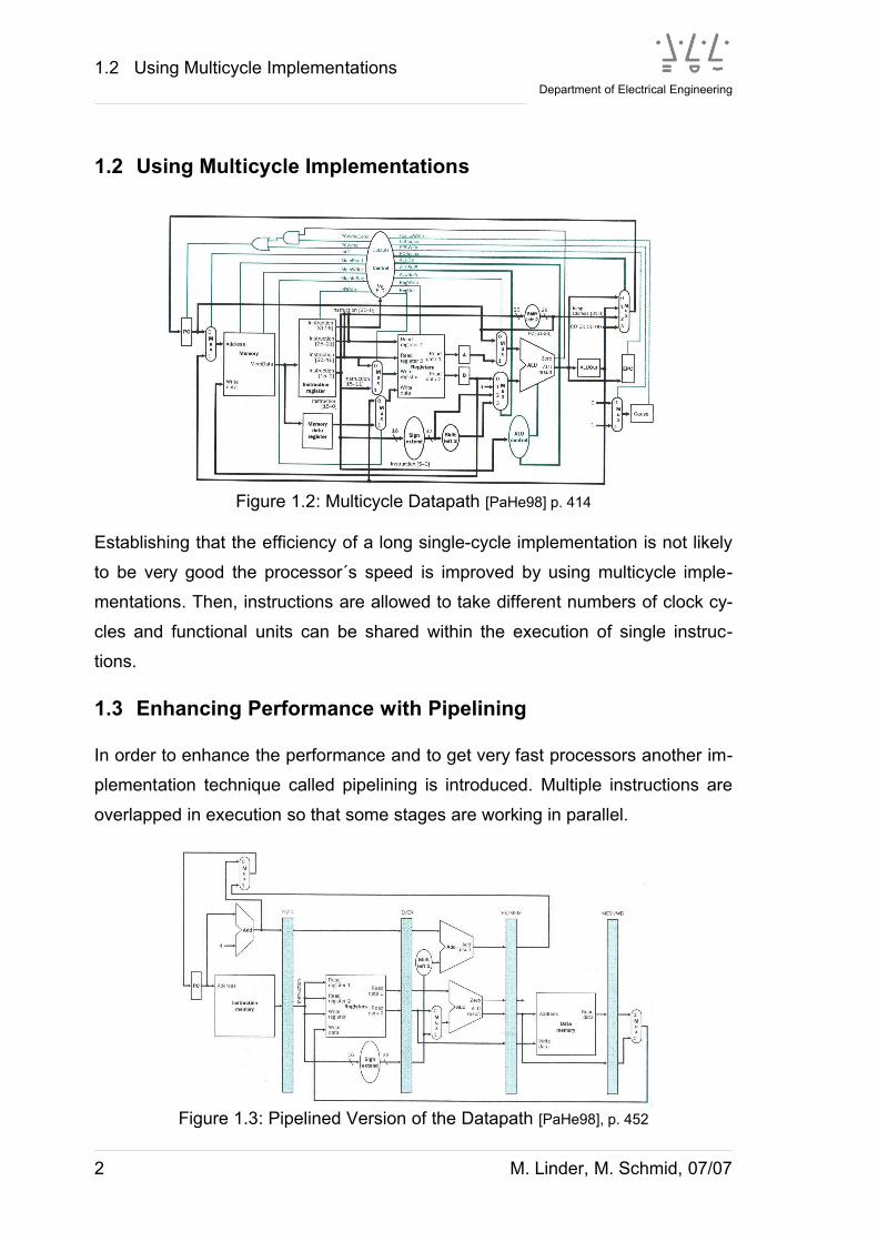
1.2 Using Multicycle Implementations
1.2 Using Multicycle Implementations
Establishing that the efficiency of a long single-cycle implementation is not likely
to be very good the processor´s speed is improved by using multicycle imple-
mentations. Then, instructions are allowed to take different numbers of clock cy-
cles and functional units can be shared within the execution of single instruc-
tions.
1.3 Enhancing Performance with Pipelining
In order to enhance the performance and to get very fast processors another im-
plementation technique called pipelining is introduced. Multiple instructions are
overlapped in execution so that some stages are working in parallel.
2 M. Linder, M. Schmid, 07/07
Figure 1.2: Multicycle Datapath [PaHe98] p. 414
Figure 1.3: Pipelined Version of the Datapath [PaHe98], p. 452
Department of Electrical Engineering

2 Target Specification
2 Target Specification
2.1 Building a Datapath
2.1.1 Major Components
At first we look at the elements required to execute the MIPS instructions and
their connection.
The first element needed is a place to store the program instructions. This In-
struction Memory is used to hold and supply instructions given an address.
The address must be kept in the Program Counter (PC), and in order to incre-
ment the PC to the address of the next instruction, we also need an Adder.
All these elements are shown in figure 2.1.
After fetching one instruction from the instruction memory, the program counter
has to be incremented so that it points to the address of the next instruction 4
bytes later.
This is realised by the datapath shown in figure 2.2.
M. Linder, M. Schmid, 07/07 3
Figure 2.1: Instruction Memory, Program Counter and Adder [Pa-He98], p 344
Figure 2.2: Datapath for fetching instructions and incrementing the PC[PaHe98] p. 345
Department of Electrical Engineering

2.1 Components for Arithmetic and Logic Functions
2.1.2 Components for Arithmetic and Logic Functions
The instructions we use all read two registers, perform an ALU operation and
write back the result.
These arithmetic-logical instructions are also called R-type instructions
([PaHe98] p. 154). This instruction class considers add, sub, slt, and and or.
The 32 registers of the processor are stored in a Register File. To read a data-
word two inputs and two outputs are needed. The inputs are 5 bits wide and
specify the register number to be read, the outputs are 32 bits wide and carry the
value of the register.
To write the result back two inputs are needed: one to specify the register num-
ber and one to supply the data to be written. The Register is shown in Figure 2.3.
To process the data from the Register, an ALU with two data inputs is used.
Figure 2.4 shows the combination of Register and ALU to operate on R-type in-
structions.
4 M. Linder, M. Schmid, 07/07
Figure 2.3: Register and ALU [PaHe98] p. 346
Figure 2.4: Datapath for R-type Instructions [PaHe98] p. 347
Department of Electrical Engineering

2.1 Load word (lw) and store word (sw) instructions
2.1.3 Load word (lw) and store word (sw) instructions
Two more elements are needed to implement the sw- and lw-instructions: the
Data Memory and the Sign Extension Unit.
The sw- and lw-instructions compute a memory address by adding a register val-
ue to the 16-bit signed offset field contained in the instruction.
Because the ALU has 32-bit values, the instruction offset field must be sign ex-
tended from 16 to 32 bits simply by concatenating the sign-bit 16 times to the
original value.
The instruction field for a lw- or sw-instruction is shown in figure 2.6:
op rs rt address6 bits 5 bits 5 bits 16 bits
Figure 2.6: Load or Store Word instruction field
M. Linder, M. Schmid, 07/07 5
Figure 2.5: Data Memory and Sign extension unit [PaHe98] p. 348
Figure 2.7: Datapath for Load Word and Store Word [PaHe98] p. 348
Department of Electrical Engineering

2.1 Branch on equal instruction
2.1.4 Branch on equal instruction
The beq instruction has three operands, two registers that are compared for
equality, and a 16-bit offset used to compute the branch target address relative
to the branch instruction address.
Figure 2.8 shows the datapath for a branch on equal instruction. This datapath
must do two operations: compare the register contents and compute the branch
target.
Therefore two things must be done: The address field of the branch instruction
must be sign extended from 16 bits to 32 bits and must be shifted left 2 bits so
that it is a word offset.
The branch target address is computed by adding the address of the next in-
struction (PC + 4) to the before computed offset.
2.1.5 Jump Instruction
The jump instruction is similar to the branch instruction, but computes the target
PC differently and not conditional.
The destination address for a jump is formed by concatenating the upper 4 bits
of the current PC + 4 to the 26-bit address field in the jump instruction (see figure
2.10 on page 8) and adding “00” as the last two bits.
6 M. Linder, M. Schmid, 07/07
Figure 2.8: Datapath for a branch instruction [PaHe98] p. 350
Department of Electrical Engineering

2.2 Simple Implementation Scheme
2.2 Simple Implementation Scheme
The simplest possible implementation of the MISP Processor contains the datap-
ath segments explained above added by the required control lines.
2.2.1 Creating a Single Datapath
The simplest datapath might attempt to execute all instructions in one clock cy-
cle. This means that any element can be used only once per instruction. So
these elements have to be duplicated.
If possible datapath elements can be shared by different instruction flows. There-
fore multiple connections to the input must be realised. This is commonly done
by a multiplexer.
Figure 2.9 shows the combined datapath including a memory of instructions and
one for data, the ALU, the PC-unit and the mentioned multiplexers.
M. Linder, M. Schmid, 07/07 7
Figure 2.9: Completed Simple Datapath [PaHe98] p. 353
Department of Electrical Engineering

2.2 ALU Control
2.2.2 ALU Control
The MIPS field that contains the information about the instruction has the follow-
ing structure:
op rs rt rd shamt funct6 bits 5 bits 5 bits 5 bits 5 bits 6 bits
Figure 2.10: MIPS field
The meaning of the fields are:
• op: basic operation
• rs: first register source
• rt: second register source
• rd: register destination
• shamt: shift amount
• funct: function
Instructionopcode ALUOp
Instructionoperation Funct field
DesiredALU action
ALU controlinput
LW 00 load word XXXXXX add 010
SW 00 store word XXXXXX add 010
Branch equal 01 branch equal XXXXXX subtract 110
R-type 10 add 100000 add 010
R-type 10 subtract 100010 subtract 110
R-type 10 AND 100100 and 000
R-type 10 OR 100101 or 001
R-type 10 set on less than 101010 set on less than 111
Figure 2.11: Table for ALU Control
Figure 2.11 shows in the last column the 3-bit ALU control input.
It depends on the 6-bit funct field of the MIPS instruction and the 2-bit ALUOp
signal generated form the Main Control Unit (see Chapter 2.2.3).
Figure 2.12 shows the datapath including the ALU Control Unit.
8 M. Linder, M. Schmid, 07/07
Department of Electrical Engineering

2.2 ALU Control
2.2.3 Main Control
The main control unit generates the control bits for the multiplexers, the data
memory and the ALU control unit.
The input of the main control unit is the 6-bit op-field of the MIPS instruction field
(see figure 2.9 on page 7).
Figure 2.13 shows the meaning of the several control signals.
Signal name Effect when deasserted Effect when asserted
RegDst The register destination number for the Write re-gister comes from the rt field (bits 20-16).
The register destination number for the Write re-gister comes from the rd field (bits 15-11).
RegWrite None The register on the Write register input is written with the value on the Write data input.
ALUSrc The second ALU operand comes from the se-cond register file output (Read data 2).
The second ALU operand is the sign-extended, lower 16 bits of the instruction.
PCSrc The PC is replaced by the output of the adder that computes the value of PC + 4.
The PC is replaced by the output of the adder that computes the branch target.
MemRead None Data memory contents designated by the ad-dress input are put on the Read data output.
MemWrite None Data memory contents designated by the ad-dress input are replaced by the value on the Wri-te data input.
MemtoReg The value fed to the register Write data input co-mes from the ALU.
The value fed to the register Write data input co-mes from the data memory.
Figure 2.13: Meaning of the main control signals [PaHe98] p. 359
M. Linder, M. Schmid, 07/07 9
Figure 2.12: Datapath with ALU Control Unit [PaHe98] p. 358
Department of Electrical Engineering

2.2 Main Control
The connection of the main control unit is shown in figure 2.14. This and the
meaning of the signals described in figure 2.13 leads directly to the truth table for
the main control unit shown in figure 2.15.
Instruction RegDst ALUSrcMemto-
RegReg
WriteMemRead
MemWrite Branch ALUOp1 ALUOp2
R-format 1 0 0 1 0 0 0 1 0
lw 0 1 1 1 1 0 0 0 0
sw X 1 X 0 0 1 0 0 0
beq X 0 X 0 0 0 1 0 1
Figure 2.15: Truth table of the main control unit [PaHe98] p. 361
2.2.4 Disadvantages of a Single-Cycle Implementation
In modern designs a single cycle implementation of a processor is not used, be-
cause it is inefficient.
A clock cycle must have the same length for every instruction and therefore it is
determined by the longest possible path. Almost this is the path of the load word
instruction which uses five functional units in series: the instruction memory, the
register file, the ALU, the data memory and the register file again.
However a single cycle implementation can be used for a small instruction set.
But if the machine gets more powerful there can be used thousands of functional
units and then the longest path causes the cycle time.
10 M. Linder, M. Schmid, 07/07
Figure 2.14: The simple datapath with the control unit [PaHe98] p. 360
Department of Electrical Engineering

2.3 Multicycle Implementation
2.3 Multicycle Implementation
To avoid the disadvantages of the single cycle implementation described in the
section before, a multicycle implementation is used.
This technique divides each instruction into steps and each step is executed in
one clock cycle.
The multicycle implementation allows a functional unit to be used more than
once in a instruction, so that the number of functional units can be reduced.
The major advantage of a multicycle design is the ability to share functional units
within an execution.
2.3.1 Additions and Changes in the Scheme
Figure 2.16 shows a abstract design of a multicycle datapath.
Comparing to the single-cycle datapath the differences are that only one memory
unit is used for instructions and data, there is only one ALU instead of an ALU
and two adders and several output registers are added to hold the output value
of a unit until it is used in a later clock cycle.
The instruction register (IR) and the memory data register (MDR) are added to
save the output of the memory. The registers A and B hold the register operands
read form the register file and the ALUOut holds the output of the ALU.
With exception of the IR all these registers hold data only between a pair of
adjacent clock cycles.
M. Linder, M. Schmid, 07/07 11
Figure 2.16: Abstract view of a multicycle desing [PaHe98] p. 378
Department of Electrical Engineering

2.3 Additions and Changes in the Scheme
Because the IR holds the value during the whole time of the execution of a
instruction, it requires a write control signal.
The reduction from former three ALUs to one causes also the following changes
in the datapath:
An additional multiplexer is added for the first ALU input to choose between the
A register and the PC.
The multiplexer at the second ALU input is changed from a two-way to a four-
way multiplexer. The two new inputs are a constant 4 to increment the PC and
the sign-extended and shifted offset field for the branch instruction.
In order to handle branches and jumps more additions in the datapath are
required.
The three cases of R-type instructions, branch instruction and jump instruction
cause three different values to be written into the PC:
• The output of the ALU which is PC + 4 should be stored directly to the PC.
• The register ALUOut after computing the branch target address.
• The lower 26 bits of the IR shifted left by two and concatenated with the
upper 4 bits of the incremented PC, when the instruction is jump.
If the instruction is branch, the write signal for the PC is conditional. Only if the
the two compared registers are equal, the computed branch address has to be
written to the PC.
Therefore the PC needs two write signals, which are PCWrite if the write is
unconditional (value is PC + 4 or jump instruction) and PCWriteCond if the write
is conditional.
12 M. Linder, M. Schmid, 07/07
Department of Electrical Engineering

2.3 Additions and Changes in the Scheme
Figure 2.17 shows the completed datapath for a multicycle implementation
including the whole control.
It also shows that the write signal for the PC is combined form the ALU zero bit
and the two write signals PCWrite and PCWriteCond by an AND gate and OR
gate.
M. Linder, M. Schmid, 07/07 13
Figure 2.17: Complete Datapath for multicycle design [PaHe98] p. 383
Department of Electrical Engineering

2.3 Execution of Instructions in Clock Cycles
2.3.2 Execution of Instructions in Clock Cycles
The execution of an instruction is broken into clock cycles, that means that each
instruction is divided into a series of steps.
Therefore the setting of the control signals are shown in figures 2.18 and 2.19.
Signal name Effect when deasserted Effect when asserted
RegDst The register file destination number for the Write register comes from the rt field
The register file destination for the Write register comes from the rd field
RegWrite None The general-purpose register selected by the Wri-te register number is written with the value of the Write data input.
ALUSrcA The first ALU operand is the PC The first ALU operand comes from the A register
MemRead None Content of memory at the location specified by the Address input is put on Memory data output.
MemWrite None Memory contents at the location specified by the Address input is replaced by value on Write data input.
MemtoReg The value fed to the register file Write data input comes from ALUOut.
The value fed to the register file Write data input comes from the MDR.
IorD The PC is used to supply the address to the me-mory unit.
ALUOut is used to supply the address to the me-mory unit.
IRWrite None The output of the memory is written into the IR.
PCWrite None The PC is written; the source is controlled byPCSource.
PCWriteCond None The PC is written if the Zero output from the ALU is also active.
Figure 2.18: Actions of 1-bit control signals [PaHe98] p. 384
Signal name Value Effect
ALUOp 00 The ALU performs an add operation.
01 The ALU performs an subtract operation.
10 The function field of the instruction determines the ALU operation.
ALUSrcB 00 The second input to the ALU comes from the B register.
01 The second input to the ALU is the constant 4.
10 The second input to the ALU is the sign-extended, lower 16 bits of the IR.
11 The second input to the ALU is the sign-extended, lower 16 bits of the IR shifted left2 bits.
PCSource 00 Output of the ALU (PC + 4) is sent to the PC for writing.
01 The contents of ALUOut (the branch target address) are sent to the PC for writing.
10 The jump target address (IR[25-0] shifted left 2 bits and concatenated withPC +4[31-28]) is sent to the PC for writing.
Figure 2.19: Actions of 2-bit control signals [PaHe98] p. 384
14 M. Linder, M. Schmid, 07/07
Department of Electrical Engineering

2.3 Execution of Instructions in Clock Cycles
The execution of an instruction is divided into maximal five steps.
Different elements of the datapath can work in parallel during one clock cycle,
whereas others can only be used in series.
So there must be sure, that after one step the values computed are stored either
in the memory or in one of the registers.
The operation steps are:
1. Instruction fetch step
Fetch the instruction from the memory and computed the address of the
sequential instruction:IR = Memory[PC]PC = PC + 4
Control signal setting:MemRead = 1IRWrite = 1IorD = 0ALUSrcA = 1ALUSrcB = 01ALUOp = 00PCSource = 00PCWrite = 1
2. Instruction decode and register fetch step
It is still unknown what the instruction is, so there can only be performed
actions that are applicable for all instructions or are not harmful.
The registers indicated by the rs and rd field of the instruction are read
and store into the A and B register, and the potential branch target is
computed and stored into the ALUOut register.A = Reg[IR[25-21]]B = Reg[IR[20-16]]ALUOut = PC + (sign-extend (IR[15-0]) << 2)
Control signal setting:ALUSrcA = 0ALUSrcB = 11ALUOp = 00
M. Linder, M. Schmid, 07/07 15
Department of Electrical Engineering

2.3 Execution of Instructions in Clock Cycles
3. Execution, memory address computation or branch completion
In this step the instruction is known and the operation depends on what
the instruction is. One of these four functions is executed:
1. Memory reference:ALUOut = A + sign-extend(IR[15-0])
Control signal setting:ALUSrcA = 1ALUSrcB = 10ALUOp = 00
2. Arithmetic-logical instruction:ALUOut = A op B
Control signal setting:ALUSrcA = 1ALUSrcB = 00ALUOp = 10
3. Branch:if (A == B) PC = ALUOut
Control signal setting:ALUSrcA = 1ALUSrcB = 00ALUOp = 01PCWriteCond = 1PCSource = 01
4. Jump:PC = PC[31-28] & (IR[25-0] << 2)
Control signal setting:PCWrite = 1
16 M. Linder, M. Schmid, 07/07
Department of Electrical Engineering

2.3 Execution of Instructions in Clock Cycles
4. Memory access or R-type instruction completion step
In this step a load or store instruction accesses memory or a arithmetic-
logical instruction writes its result.
1. Memory reference:MDR = Memory [ALUOut]orMemory [ALUOut] = B
Control signal setting:
MemRead = 1 or MemWrite = 1IorD = 1
2. Arithmetic-logical instruction:Reg[IR[15-11]] = ALUOut
Control signal setting:RegDst = 1RegWrite = 1MemtoReg = 0
5. Memory read completion step
The load instruction is completed by writing back the value from the
memory:Reg[IR[20-16]] = MDR
Control signal setting:MemtoReg = 1RegWrite = 1RegDst = 0
These five steps are summarised in figure 2.20.
M. Linder, M. Schmid, 07/07 17
Department of Electrical Engineering

2.3 Execution of Instructions in Clock Cycles
Step name Action for R-typeinstructions
Action for memory-reference instructions
Action forbranches
Action forjumps
Instruction fetch IR = Memory[PC]PC = PC + 4
Instruction decoderegister fetch
A = Reg[IR[25-21]]B = Reg[IR[20-16]]
ALUOut = PC + (sign-extend(IR[15-0] << 2)
Execution, address computation, branch/jump completi-on
ALUOut = A op B ALUOut = A + sign-extend(IR[15-0])
if (A == B) then PC = ALUOut
PC = PC[31-28] || (IR[25-0] << 2)
Memory access or R-type completion
Reg[IR[15-11]] = ALUOut
Load: MDR = Memory[ALUOut]or
Store: Memory[ALUOut] = B
Memory read comple-tion
Load: Reg[IR[20-16]] = MDR
Figure 2.20: Summary of the multicycle steps [PaHe98] p. 389
2.3.3 Defining the Control by a Finite State Machine
In the single step implementation the control was defined by simple truth tables
that set the control signals depending on the instruction.
This does not work for a mulitcycle datapath.
The control is more complex, because it must specify both the signals to be set
in any step and the next step in the sequence.
Therefore a finite state machine is used.
Figure 2.21 shows the finite state machine for the control of the multicycle
datapath implementation.
18 M. Linder, M. Schmid, 07/07
Department of Electrical Engineering

2.3 Defining the Control by a Finite State Machine
The setting of the control signals is also shown in figure 2.21.
All unused signals have to be deasserted or keep their value during the next
states until they are set again.
All signal settings in all states is shown in figure 2.22.
M. Linder, M. Schmid, 07/07 19
Figure 2.21: Complete finite state machine control [PaHe98] p. 396
Department of Electrical Engineering

2.3 Defining the Control by a Finite State Machine
Signal name State
0 1 2 3 4 5 6 7 8 9
RegDst 0 0 0 0 0 0 0 1 0 0
RegWrite 0 0 0 0 1 0 0 1 0 0
ALUSrcA 0 0 1 1 1 1 1 1 1 0
MemRead 1 0 0 1 0 0 0 0 0 0
MemWrite 0 0 0 0 0 1 0 0 0 0
MemtoReg 0 0 0 0 1 0 0 0 0 0
IorD 0 0 0 1 0 1 0 0 0 0
IRWrite 1 0 0 0 0 0 0 0 0 0
PCWrite 1 0 0 0 0 0 0 0 0 1
PCWriteCond 0 0 0 0 0 0 0 0 1 0
ALUOp 00 00 00 00 00 00 10 10 01 00
ALUSrcB 01 11 10 10 10 10 00 00 00 11
PCSource 00 00 00 00 00 00 00 00 01 10
Figure 2.22: Setting of Control Signals
20 M. Linder, M. Schmid, 07/07
Department of Electrical Engineering

3 Design Tasks
3 Design Tasks
• Block Diagram of first hierarchy levels
• Register Transfer Level Models implemented in pure VHDL
• VHDL Testbench of important RTL Models
• Implementation in Altera Target Technology
• Prototype Testing
• Simulation Tool: ModelSim
• Synthesis Tool: Altera Quartus
• Milestone Presentations
• Design Project Report in OpenOffice Document Format
• Design Directory Structure is mandatory according to the following table:
Object Description
toplevel Root directory for a VHDL design projecttoplevel/src directory for VHDL source codetoplevel/work directory for VHDL working library, contains compiled object code of
ModelSim VHDL compilertoplevel/simulation simulation resultstoplevel/stimuli stimuli files of extended simulation runs should be stored in
this directorytoplevel/pnr data produced after a place&route run can be found in this directorytoplevel/scripts scriptfiles for automated batch processing of the design steps
should be placed heretoplevel/log log files of the different design stepstoplevel/doc directory for project documentation, data sheets, etc.
M. Linder, M. Schmid, 07/07 21
Department of Electrical Engineering

4 Module Specification
4 Module Specification
4.1 ALU
4.1.1 Functional Description
The arithmetic-logic unit (ALU) performs basic arithmetic and logic operations
which are controlled by the opcode. The result of the instruction is written to the
output. An additional zero-bit signalizes an high output if the result equals zero.
At the present time, the basic arithmetic operations add and sub and the logic
operations and, or and slt can be applied to inputs. The inputs are 32 bit wide
with type unsigned. A detection of overflow or borrow is not supported at the mo-
ment.
22 M. Linder, M. Schmid, 07/07
Department of Electrical Engineering

4.1 Block Diagram
4.1.2 Block Diagram
M. Linder, M. Schmid, 07/07 23
Department of Electrical Engineering
Figure 4.1: ALU 1/3

4.1 Block Diagram
24 M. Linder, M. Schmid, 07/07
Department of Electrical Engineering
Figure 4.2: ALU 2/3

4.1 Block Diagram
M. Linder, M. Schmid, 07/07 25
Department of Electrical Engineering
Figure 4.3: ALU 3/3

4.1 Simulation Results
4.1.3 Simulation Results
4.1.4 Design Files
File Name File Type Description
e_alu.vhda_alu_behave.vhd
VHDL Source Files Arithmetic-logic unit
t_alu.vhd VHDL Testbench File Testbench for single operations
t_alu_fileio.vhd VHDL Testbench File Testbench using file I/O
26 M. Linder, M. Schmid, 07/07
Figure 4.4: Simulation Results of ALU
Department of Electrical Engineering

4.2 Memory
4.2 Memory
4.2.1 Functional Description
Data is synchronously written to or read from the memory with a data bus width
of 32 bit. The memory consists of four ram blocks with 8 bit data width each.
A control signal enables the memory to be written, otherwise data is only read. In
order to store data to the memory the data word is subdivided into four bytes
which are separately written to the ram blocks. Vice versa, the single bytes are
concatenated to get the data word back again.
At the moment, it is only possible to read and write data words. An addressing of
half-words or single bytes is not allowed. In order to write or read data words, all
ram blocks have to be selected. Hence, the lowest two bit are not examined for
chip-select logic.
Data is addressed by the MIPS-processor with an address width of 32 bit, while
the address width of a ram block is 8 bit each. All ram blocks are connected to
the same address, namely from mem_address(9 downto 2). Since we do not use
the full address width for addressing and chip selects, data words are addressed
by multiple addresses.
Unfortunately, some problems occurred during simulation of the memory unit.
According to the MIPS design shown in literature [PaHe98], there should be im-
plemented a memory unit with an unregistered output. The Altera Quartus
MegaWizard Plug-In Manager yielded a ram block with a synchronous output
(a_ram_syn.vhd) , although the output was defined as unregistered.
In order to get an unregistered memory output, another ram block was defined in
VHDL code (a_ram_rtl.vhd). There, the output directly yields the data being ad-
dressed by the unregistered input address. Unfortunately, the synthesizer does
not support memory initialisation files in the RTL-code for setting data to the
memory. Hence, it was not possible to implement the memory in real hardware.
M. Linder, M. Schmid, 07/07 27
Department of Electrical Engineering

4.2 Block Diagram
4.2.2 Block Diagram
4.2.3 Simulation Results
Figure 4.6 shows the simulation results with registered data output.
28 M. Linder, M. Schmid, 07/07
Figure 4.5: Memory
Figure 4.6: Simulation Results of Memory (registered outputs)
Department of Electrical Engineering
4.2 Simulation Results
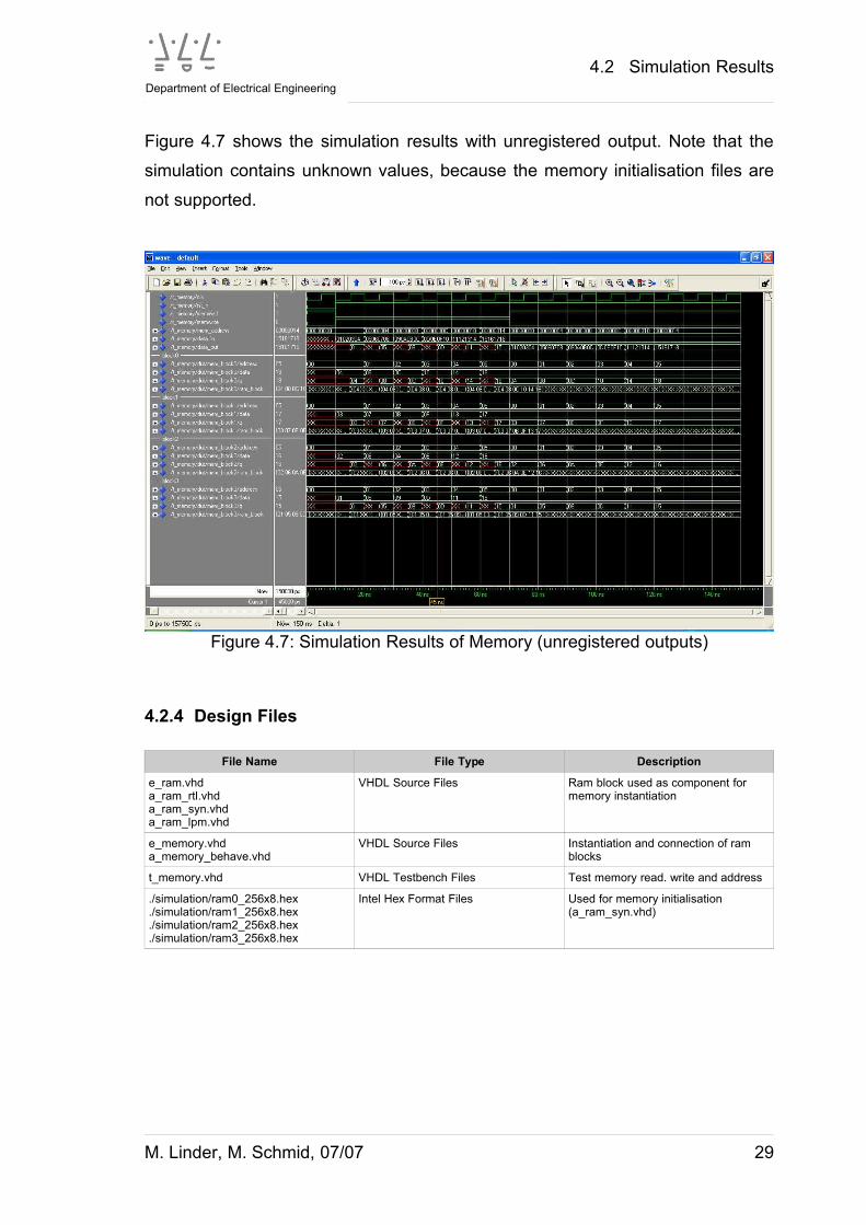
Figure 4.7 shows the simulation results with unregistered output. Note that the
simulation contains unknown values, because the memory initialisation files are
not supported.
4.2.4 Design Files
File Name File Type Description
e_ram.vhda_ram_rtl.vhda_ram_syn.vhda_ram_lpm.vhd
VHDL Source Files Ram block used as component for memory instantiation
e_memory.vhda_memory_behave.vhd
VHDL Source Files Instantiation and connection of ram blocks
t_memory.vhd VHDL Testbench Files Test memory read. write and address
./simulation/ram0_256x8.hex
./simulation/ram1_256x8.hex
./simulation/ram2_256x8.hex
./simulation/ram3_256x8.hex
Intel Hex Format Files Used for memory initialisation (a_ram_syn.vhd)
M. Linder, M. Schmid, 07/07 29
Department of Electrical Engineering
Figure 4.7: Simulation Results of Memory (unregistered outputs)
4.3 Control
4.3 Control
4.3.1 Functional Description
The control of the processor is realised by a Finite State Machine described in
section 2.3.3.
The input to the State Machine are the upper 6 bits of the function field contain-
ing the instruction.
The outputs of the state machine are the control signals of the single functional
units of the processor implementation especially the multiplexers of the datapath.
The Operation Code of the ALU is stored in a truth table and the corresponding
Opcode is produced depending on the ALUOp signal of the state machine and
the lower 6 bits of the function field containing the information which of the arith-
metic or logic instruction is to use.
30 M. Linder, M. Schmid, 07/07
Department of Electrical Engineering

4.3 State Diagram
4.3.2 State Diagram
An additional Error State is inserted which is a deadlock. If any unknown instruc-
tion occurs the Error State is entered.
M. Linder, M. Schmid, 07/07 31
Figure 4.8: Control Finite State Machine
ErrorState
Department of Electrical Engineering

4.3 Block Diagram
4.3.3 Block Diagram
32 M. Linder, M. Schmid, 07/07
Figure 4.9: Control FSM
Department of Electrical Engineering
Figure 4.10: ALU Control

4.3 Block Diagram
4.3.4 Simulation Results
4.3.5 Design Files
File Name File Type Description
e_control_ControlFSM.vhda_control_ControlFSM.vhd
VHDL Source Files Finite State Machine for Control
e_control_ALUControl.vhda_control_ALUControl.vhd
VHDL Source Files Truth Tabel for ALU Control
e_control.vhda_control.vhd
VHDL Source Files Controlpath
M. Linder, M. Schmid, 07/07 33
Figure 4.11: Control
Figure 4.12: Simulation Results of the Control FSM
Department of Electrical Engineering

4.4 Data Path
4.4 Data Path
The datapath is divided into four sections with respect to the pipelining structure
of a processor. The four parts are the Instruction Fetch, Instruction Decode, Exe-
cution and Memory Writeback.
These sections are synthesized of their own and then combined to the Data
Block.
4.4.1 Instruction Fetch
4.4.1.1 Functional Description
The Instruction Fetch Block contains the PC the Instruction Register and the
Memory Data Register.
This part provides the data and instruction form the memory.
4.4.1.2 Block Diagram
34 M. Linder, M. Schmid, 07/07
Figure 4.13: Instruction Fetch
Department of Electrical Engineering

4.4 Instruction Fetch
4.4.1.3 Design Files
File Name File Type Description
e_pc.vhda_pc_behave.vhd
VHDL Source Files Program Counter
e_tempreg.vhda_tempreg_behave.vhd
VHDL Source Files Temporary Memory Data Register
e_instreg.vhda_instreg_behave.vhd
VHDL Source Files Instruction Register
e_data_fetch.vhda_data_fetch_behave_vhd
VHDL Source Files Instruction Fetch Block
4.4.2 Instruction Decode
4.4.2.1 Functional Description
The Instruction Decode Block writes the instruction of the Instruction Register to
the Register File and computes the second operand for a Branch Instruction or a
sw- or lw-instruction.
4.4.2.2 Block Diagram
M. Linder, M. Schmid, 07/07 35
Figure 4.14: Instruction Decode
Department of Electrical Engineering

4.4 Instruction Decode
4.4.2.3 Design Files
File Name File Type Description
e_regfile.vhda_regfile_behave.vhd
VHDL Source Files Register File
e_tempreg.vhda_tempreg_behave.vhd
VHDL Source Files Temporary Memory Data Register
e_data_decode.vhda_data_decode_behave.vhd
VHDL Source Files Data Decode Block
4.4.3 Execution
4.4.3.1 Functional Description
The Execution contains the ALU as main element and computes the desired re-
sult of the instruction.
It also computes the jump target address and provides it for the Memory Write-
back Block.
The operands loaded to the ALU are chosen by two multiplexers which are sen-
sible to the signals ALUSrcA and ALUSrcB.
36 M. Linder, M. Schmid, 07/07
Department of Electrical Engineering

4.4 Execution
4.4.3.2 Block Diagram
M. Linder, M. Schmid, 07/07 37
Department of Electrical Engineering
Figure 4.15: Execution

4.4 Execution
4.4.3.3 Design Files
File Name File Type Description
e_alu.vhda_alu_behave.vhd
VHDL Source Files ALU
e_data_execution.vhda_data_execution.vhd
VHDL Source Files Execution Block
38 M. Linder, M. Schmid, 07/07
Department of Electrical Engineering

4.4 Memory Writeback
4.4.4 Memory Writeback
4.4.4.1 Functional Description
The Memory Writeback Block consists of the ALUOut register and a multiplexer
with source signal PCSource.
This block leads the result of the computation either back to memory or to the
register file.
The multiplexer leads back the next PC value depending on the PCSource sig-
nal.
M. Linder, M. Schmid, 07/07 39
Department of Electrical Engineering

4.4 Memory Writeback
4.4.4.2 Block Diagram
40 M. Linder, M. Schmid, 07/07
Department of Electrical Engineering
Figure 4.16: Memory Writeback

4.4 Memory Writeback
4.4.4.3 Design Files
File Name File Type Description
e_tempreg.vhda_tempreg_behave.vhd
VHDL Source Files Temporary ALUOut Register
e_data_memwriteback.vhda_data_memwriteback.vhd
VHDL Source Files Memory Writeback Block
M. Linder, M. Schmid, 07/07 41
Department of Electrical Engineering

4.4 Data Path
4.4.5 Data Path
4.4.5.1 Block Diagram
4.4.5.2 Design Files
File Name File Type Description
e_data.vhda_data_vhd
VHDL Source Files Datapath
e_data_fetch.vhda_data_fetch.vhd
VHDL Source Files Data Fetch Block
e_data_decode.vhda_data_decode.vhd
VHDL Source Files Data Decode Block
e_data_execution.vhda_data_execution.vhd
VHDL Source Files Data Execution Block
e_data_memwriteback.vhda_data_memwriteback.vhd
VHDL Source Files Memory Writeback Block
e_tempreg.vhda_tempreg_behave.vhd
VHDL Source Files Temporary ALUOut Register
e_alu.vhda_alu_behave.vhd
VHDL Source Files ALU
e_regfile.vhda_regfile_behave.vhd
VHDL Source Files Register File
e_pc.vhda_pc_behave.vhd
VHDL Source Files Program Counter
e_instreg.vhda_instreg_behave.vhd
VHDL Source Files Instruction Register
42 M. Linder, M. Schmid, 07/07
Department of Electrical Engineering

4.5 Processor and Memroy
4.5 Processor and Memroy
4.5.1 Functional Description
The both parts Datapath and Controlpath are combined to the processing unit.
Together with the Memory the whole processor is completed.
4.5.2 Block Diagram
M. Linder, M. Schmid, 07/07 43
Department of Electrical Engineering
Figure 4.17: Processing Unit (Datapath & Controlpath)
Figure 4.18: Processing Unit & Memory

4.5 Design Files
4.5.3 Design Files
File Name File Type Description
e_control_ControlFSM.vhda_control_ControlFSM.vhd
VHDL Source Files Finite State Machine for Control
e_control_ALUControl.vhda_control_ALUControl.vhd
VHDL Source Files Truth Tabel for ALU Control
e_control.vhda_control.vhd
VHDL Source Files Controlpath
e_data.vhda_data.vhd
VHDL Source Files Datapath
e_data_fetch.vhda_data_fetch.vhd
VHDL Source Files Data Fetch Block
e_data_decode.vhda_data_decode.vhd
VHDL Source Files Data Decode Block
e_data_execution.vhda_data_execution.vhd
VHDL Source Files Data Execution Block
e_data_memwriteback.vhda_data_memwriteback.vhd
VHDL Source Files Memory Writeback Block
e_tempreg.vhda_tempreg_behave.vhd
VHDL Source Files Temporary ALUOut Register
e_alu.vhda_alu_behave.vhd
VHDL Source Files ALU
e_regfile.vhda_regfile_behave.vhd
VHDL Source Files Register File
e_pc.vhda_pc_behave.vhd
VHDL Source Files Program Counter
e_instreg.vhda_instreg_behave.vhd
VHDL Source Files Instruction Register
e_ram.vhda_ram_rtl.vhda_ram_syn.vhda_ram_lpm.vhd
VHDL Source Files Ram block used as component for memory instantiation
t_procmem.vhdt_procmem_init.vhd
VHDL Testbench Files Testbench for testing the processor
44 M. Linder, M. Schmid, 07/07
Department of Electrical Engineering

5 Synthesis Results
5 Synthesis Results
+------------------------------------------------------------------------------+; Analysis & Synthesis Summary ;+------------------------------------+-----------------------------------------+; Analysis & Synthesis Status ; Successful - Thu Jul 05 11:15:33 2007 ;; Quartus II Version ; 7.0 Build 33 02/05/2007 SJ Full Version ;; Revision Name ; procmem ;; Top-level Entity Name ; procmem ;; Family ; Cyclone II ;; Total logic elements ; 0 ;; Total combinational functions ; 0 ;; Dedicated logic registers ; 0 ;; Total registers ; 0 ;; Total pins ; 2 ;; Total virtual pins ; 0 ;; Total memory bits ; 0 ;; Embedded Multiplier 9-bit elements ; 0 ;; Total PLLs ; 0 ;+------------------------------------+-----------------------------------------+
Figure 5.1: Analysis & Synthesis Summary
+--------------------------------------------------------------------------------------------------------------+; Analysis & Synthesis Settings ;+--------------------------------------------------------------------+--------------------+--------------------+; Option ; Setting ; Default Value ;+--------------------------------------------------------------------+--------------------+--------------------+; Device ; EP2C20F484C7 ; ;; Top-level entity name ; procmem ; procmem ;; Family name ; Cyclone II ; Stratix ;; Restructure Multiplexers ; Auto ; Auto ;; Create Debugging Nodes for IP Cores ; Off ; Off ;; Preserve fewer node names ; On ; On ;; Disable OpenCore Plus hardware evaluation ; Off ; Off ;; Verilog Version ; Verilog_2001 ; Verilog_2001 ;; VHDL Version ; VHDL93 ; VHDL93 ;; State Machine Processing ; Auto ; Auto ;; Safe State Machine ; Off ; Off ;; Extract Verilog State Machines ; On ; On ;; Extract VHDL State Machines ; On ; On ;; Ignore Verilog initial constructs ; Off ; Off ;; Add Pass-Through Logic to Inferred RAMs ; On ; On ;; DSP Block Balancing ; Auto ; Auto ;; NOT Gate Push-Back ; On ; On ;; Power-Up Don't Care ; On ; On ;; Remove Redundant Logic Cells ; Off ; Off ;; Remove Duplicate Registers ; On ; On ;; Ignore CARRY Buffers ; Off ; Off ;; Ignore CASCADE Buffers ; Off ; Off ;; Ignore GLOBAL Buffers ; Off ; Off ;; Ignore ROW GLOBAL Buffers ; Off ; Off ;; Ignore LCELL Buffers ; Off ; Off ;; Ignore SOFT Buffers ; On ; On ;; Limit AHDL Integers to 32 Bits ; Off ; Off ;; Optimization Technique -- Cyclone II ; Balanced ; Balanced ;; Carry Chain Length -- Stratix/Stratix GX/Cyclone/MAX II/Cyclone II ; 70 ; 70 ;; Auto Carry Chains ; On ; On ;; Auto Open-Drain Pins ; On ; On ;; Perform WYSIWYG Primitive Resynthesis ; Off ; Off ;; Perform gate-level register retiming ; Off ; Off ;; Allow register retiming to trade off Tsu/Tco with Fmax ; On ; On ;; Auto ROM Replacement ; On ; On ;; Auto RAM Replacement ; On ; On ;; Auto Shift Register Replacement ; On ; On ;; Auto Clock Enable Replacement ; On ; On ;; Allow Synchronous Control Signals ; On ; On ;; Force Use of Synchronous Clear Signals ; Off ; Off ;; Auto RAM to Logic Cell Conversion ; Off ; Off ;; Auto Resource Sharing ; Off ; Off ;; Allow Any RAM Size For Recognition ; Off ; Off ;; Allow Any ROM Size For Recognition ; Off ; Off ;; Allow Any Shift Register Size For Recognition ; Off ; Off ;; Ignore translate_off and synthesis_off directives ; Off ; Off ;; Show Parameter Settings Tables in Synthesis Report ; On ; On ;; Ignore Maximum Fan-Out Assignments ; Off ; Off ;
M. Linder, M. Schmid, 07/07 45
Department of Electrical Engineering

5 Synthesis Results
; Retiming Meta-Stability Register Sequence Length ; 2 ; 2 ;; PowerPlay Power Optimization ; Normal compilation ; Normal compilation ;; HDL message level ; Level2 ; Level2 ;; Suppress Register Optimization Related Messages ; Off ; Off ;; Number of Removed Registers Reported in Synthesis Report ; 100 ; 100 ;; Use smart compilation ; Off ; Off ;+--------------------------------------------------------------------+--------------------+--------------------+
Figure 5.2: Analysis & Synthesis Settings
+-----------------------------------------------------+; Compilation Hierarchy ;+-----------------------------------------------------+; |procmem ;; |mips ;; |control:inst_control| ;; |ALUControl:inst_ALUControl| ;; |ControlFSM:inst_ControlFSM| ;; |data:inst_data| ;; |data_decode:inst_data_decode| ;; |regfile:inst_regfile| ;; |tempreg:A| ;; |tempreg:B| ;; |data_execution:inst_data_execution| ;; |alu:alu_inst| ;; |data_fetch:inst_data_fetch| ;; |instreg:instr_reg| ;; |pc:proc_cnt| ;; |tempreg:mem_data_reg| ;; |data_memwriteback:inst_data_memwriteback| ;; |tempreg:tempreg_inst| ;; |memory ;; |ram:mem_block0| ;; |altsyncram:ram_block_rtl_0| ;; |altsyncram_ia61:auto_generated| ;; |ram:mem_block1| ;; |altsyncram:ram_block_rtl_1| ;; |altsyncram_ia61:auto_generated| ;; |ram:mem_block2| ;; |altsyncram:ram_block_rtl_2| ;; |altsyncram_ia61:auto_generated| ;; |ram:mem_block3| ;; |altsyncram:ram_block_rtl_3| ;; |altsyncram_ia61:auto_generated| ;+-----------------------------------------------------+
Figure 5.3: Compilation History
46 M. Linder, M. Schmid, 07/07
Department of Electrical Engineering

6 Results of Prototype Testing
6 Results of Prototype Testing
6.1 Description
For the first test of the completed processor and the memory a simple addition of
two numbers was done.
Therefore at first the memory has to be loaded with the instructions and data by
using *.mif-files to write the information into the memory blocks before starting
the simulation.
The instructions written into the memory are:
Memory
Address Instruction
Instruction Field
op rs rt rd shamt funct
000 lw $s0, 128($zero) 1 0 0 0 1 1 0 0 0 0 0 1 0 0 0 0 0 0 0 0 0 0 0 0 1 0 0 0 0 0 0 0004 lw $s1, 132($zero) 1 0 0 0 1 1 0 0 0 0 0 1 0 0 0 1 0 0 0 0 0 0 0 0 1 0 0 0 0 1 0 0008 add $s2, $s0, $s1 0 0 0 0 0 0 1 0 0 0 0 1 0 0 0 1 1 0 0 1 0 0 0 0 0 0 1 0 0 0 0 0012 sw $s2, 136($zero) 1 0 1 0 1 1 0 0 0 0 0 1 0 0 1 0 0 0 0 0 0 0 0 0 1 0 0 0 1 0 0 0016 sub $s3, $s1, $s0 0 0 0 0 0 0 1 0 0 0 1 1 0 0 0 0 1 0 0 1 1 0 0 0 0 0 1 0 0 0 1 0020 sw $s3, 140($zero) 1 0 1 0 1 1 0 0 0 0 0 1 0 0 1 1 0 0 0 0 0 0 0 0 1 0 0 0 1 1 0 0024 and $s4, $s1, $s0 0 0 0 0 0 0 1 0 0 0 1 1 0 0 0 0 1 0 1 0 0 0 0 0 0 0 1 0 0 1 0 0028 sw $s4, 144($zero) 1 0 1 0 1 1 0 0 0 0 0 1 0 1 0 0 0 0 0 0 0 0 0 0 1 0 0 1 0 0 0 0032 or $s5, $s1, $s0 0 0 0 0 0 0 1 0 0 0 1 1 0 0 0 0 1 0 1 0 1 0 0 0 0 0 1 0 0 1 0 1036 sw $s5, 148($zero) 1 0 1 0 1 1 0 0 0 0 0 1 0 1 0 1 0 0 0 0 0 0 0 0 1 0 0 1 0 1 0 0040 slt $s6, $s1, $s0 0 0 0 0 0 0 1 0 0 0 0 1 0 0 0 1 1 0 1 1 0 0 0 0 0 0 1 0 1 0 1 0044 sw $s6, 152($zero) 1 0 1 0 1 1 0 0 0 0 0 1 0 1 1 0 0 0 0 0 0 0 0 0 1 0 0 1 1 0 0 0048 beq $s0, $s4, 56 0 0 0 1 0 0 1 0 0 0 0 1 0 1 0 0 0 0 0 0 0 0 0 0 0 0 0 0 0 0 0 1052 UNDEFINED U U U U U U U U U U U U U U U U U U U U U U U U U U U U U U U U056 j 8 0 0 0 0 1 0 0 0 0 0 0 0 0 0 0 0 0 0 0 0 0 0 0 0 0 0 0 0 0 0 1 0
The data written to the memory are:
Memory
Address Data (dec) Data (bin)
128 379 0 0 0 0 0 0 0 0 0 0 0 0 0 0 0 0 0 0 0 0 0 0 0 1 0 1 1 1 1 0 1 1132 383 0 0 0 0 0 0 0 0 0 0 0 0 0 0 0 0 0 0 0 0 0 0 0 1 0 1 1 1 1 1 1 1
M. Linder, M. Schmid, 07/07 47
Department of Electrical Engineering
6.1 Description
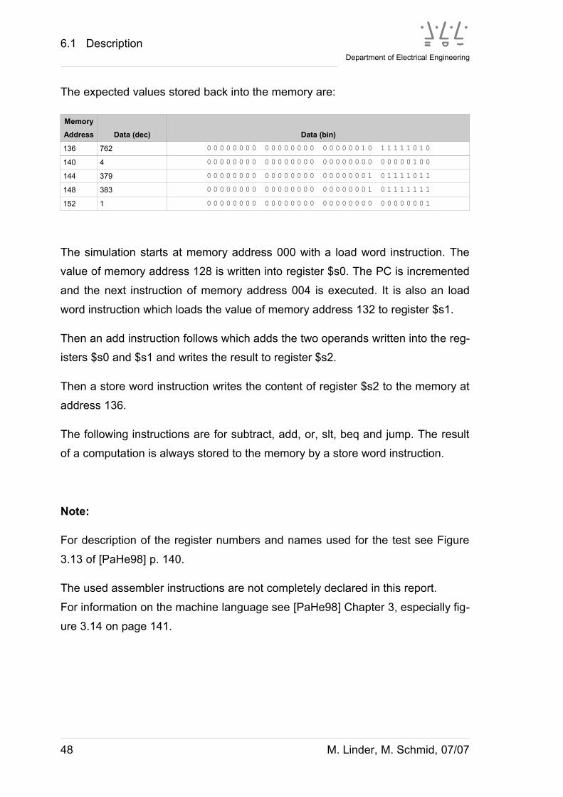
The expected values stored back into the memory are:
Memory
Address Data (dec) Data (bin)
136 762 0 0 0 0 0 0 0 0 0 0 0 0 0 0 0 0 0 0 0 0 0 0 1 0 1 1 1 1 1 0 1 0140 4 0 0 0 0 0 0 0 0 0 0 0 0 0 0 0 0 0 0 0 0 0 0 0 0 0 0 0 0 0 1 0 0144 379 0 0 0 0 0 0 0 0 0 0 0 0 0 0 0 0 0 0 0 0 0 0 0 1 0 1 1 1 1 0 1 1148 383 0 0 0 0 0 0 0 0 0 0 0 0 0 0 0 0 0 0 0 0 0 0 0 1 0 1 1 1 1 1 1 1152 1 0 0 0 0 0 0 0 0 0 0 0 0 0 0 0 0 0 0 0 0 0 0 0 0 0 0 0 0 0 0 0 1
The simulation starts at memory address 000 with a load word instruction. The
value of memory address 128 is written into register $s0. The PC is incremented
and the next instruction of memory address 004 is executed. It is also an load
word instruction which loads the value of memory address 132 to register $s1.
Then an add instruction follows which adds the two operands written into the reg-
isters $s0 and $s1 and writes the result to register $s2.
Then a store word instruction writes the content of register $s2 to the memory at
address 136.
The following instructions are for subtract, add, or, slt, beq and jump. The result
of a computation is always stored to the memory by a store word instruction.
Note:
For description of the register numbers and names used for the test see Figure
3.13 of [PaHe98] p. 140.
The used assembler instructions are not completely declared in this report.
For information on the machine language see [PaHe98] Chapter 3, especially fig-
ure 3.14 on page 141.
48 M. Linder, M. Schmid, 07/07
Department of Electrical Engineering

6.2 Simulation Result
6.2 Simulation Result
M. Linder, M. Schmid, 07/07 49
Department of Electrical Engineering
Figure 6.1: Simulation Results of MIPS and Memory

7 Conclusion
7 Conclusion
7.1 Our own experiences
While working on our miniproject, we applied a lot of knowledge learned in the
lecture VHDL. Furthermore, we gained a lot of experience in using the simulation
and synthesis tools. It was very interesting and exciting to describe real hardware
and to see the expected results in simulation and the block diagrams after syn-
thesis.
Our miniproject implementing a processor in VHDL has been a real challenge.
The complexity was not located in the single components, but rather in the imple-
mentation of the synchronous operation of the whole control and datapath. Due
to an intensive preparation of the desired hardware according to the literature
“Computer Organization & Design” [PaHe98], we prevented unintended design
errors. Since our project transcends a pure implementation of VHDL code, we
were able to gain experience in hierarchical design with component instantiation
and package design.
Additionally, while implementing a microprocessor, we could refresh our knowl-
edge in processor operations, memory addressing and MIPS instruction coding.
7.2 Annotations to “Computer Organization & Design” [PaHe98]
Since the design of our MIPS processor is closely connected to the literature
[PaHe98], we read the chapter 5 in detail. Overall, we adjusted the design as
conform as possible to the description in [PaHe98]. There are some passages
which do not provide a full description, e.g. the output signals of the control FSM
are not listed completely for each state. Nevertheless, “Computer Organization &
Design” by Patterson and Hennessy provides a brilliant composition describing
the control and datapath of a processor implementation.
50 M. Linder, M. Schmid, 07/07
Department of Electrical Engineering

7.3 Further work on the project
7.3 Further work on the project
Although we spent much more time than scheduled, we did not reach all our
aims. For further work on the project, we recommend our successors to continue
the following tasks:
– Verify the synthesis results (with VHDL code created by Quartus) with desired
behavior implemented in RTL and seen in testbench simulation in order to
obtain the desired unregistered memory output mentioned in chapter 4.2.
– Realise an hardware implementation of processor and memory in order to
verify the behavior of the desired hardware on the Cyclone II Development &
Education Board, e.g. debug the memory data.
– Introduce the pipelining of instructions described in chapter 6 [PaHe98] to im-
prove the performance of the MIPS processor.
M. Linder, M. Schmid, 07/07 51
Department of Electrical Engineering

8 Appendix
8 Appendix
8.1 Design files
8.1.1 Project Entities
LIBRARY IEEE;USE IEEE.std_logic_1164.ALL;ENTITY ControlFSM IS PORT (clk, rst_n : IN std_ulogic; instr_31_26 : IN std_ulogic_vector(5 downto 0); RegDst, RegWrite, ALUSrcA, MemRead, MemWrite, MemtoReg, IorD, IRWrite, PCWrite, PCWriteCond : OUT std_ulogic; ALUOp, ALUSrcB, PCSource : OUT std_ulogic_vector(1 downto 0) );END ControlFSM;
VHDLSource 8.1: e_control_ControlFSM.vhd
LIBRARY IEEE;USE IEEE.std_logic_1164.ALL;ENTITY ALUControl IS PORT (instr_15_0 : IN std_ulogic_vector(15 downto 0); ALUOp : IN std_ulogic_vector(1 downto 0); ALUopcode : OUT std_ulogic_vector(2 downto 0) );END ALUControl;
VHDLSource 8.2: e_control_ALUControl.vhd
LIBRARY IEEE;USE IEEE.std_logic_1164.ALL;ENTITY control IS PORT (clk, rst_n : IN std_ulogic; instr_31_26 : IN std_ulogic_vector(5 downto 0); instr_15_0 : IN std_ulogic_vector(15 downto 0); zero : IN std_ulogic; ALUopcode : OUT std_ulogic_vector(2 downto 0); RegDst, RegWrite, ALUSrcA, MemRead, MemWrite, MemtoReg, IorD, IRWrite : OUT std_ulogic; ALUSrcB, PCSource : OUT std_ulogic_vector(1 downto 0); PC_en : OUT std_ulogic );END control
VHDLSource 8.3: e_control.vhd
52 M. Linder, M. Schmid, 07/07
Department of Electrical Engineering

8.1 Project Entities
LIBRARY IEEE;USE IEEE.std_logic_1164.ALL;USE IEEE.numeric_std.ALL;-- use packageUSE work.procmem_definitions.ALL;ENTITY tempreg IS PORT ( clk : IN STD_ULOGIC; rst_n : IN STD_ULOGIC; reg_in : IN STD_ULOGIC_VECTOR(width-1 DOWNTO 0); reg_out : OUT STD_ULOGIC_VECTOR(width-1 DOWNTO 0) );END tempreg
VHDLSource 8.4: e_tempreg.vhd
LIBRARY IEEE;USE IEEE.std_logic_1164.ALL;USE IEEE.numeric_std.ALL;-- use packageUSE work.procmem_definitions.ALL;ENTITY pc IS PORT ( clk : IN STD_ULOGIC; rst_n : IN STD_ULOGIC; pc_in : IN STD_ULOGIC_VECTOR(width-1 DOWNTO 0); PC_en : IN STD_ULOGIC; pc_out : OUT STD_ULOGIC_VECTOR(width-1 DOWNTO 0) );END pc;
VHDLSource 8.5: e_pc.vhd
LIBRARY IEEE;USE IEEE.std_logic_1164.ALL;USE IEEE.numeric_std.ALL;-- use packageUSE work.procmem_definitions.ALL;ENTITY instreg IS PORT ( clk : IN STD_ULOGIC; rst_n : IN STD_ULOGIC; memdata : IN STD_ULOGIC_VECTOR(width-1 DOWNTO 0); IRWrite : IN STD_ULOGIC; instr_31_26 : OUT STD_ULOGIC_VECTOR(5 DOWNTO 0); instr_25_21 : OUT STD_ULOGIC_VECTOR(4 DOWNTO 0); instr_20_16 : OUT STD_ULOGIC_VECTOR(4 DOWNTO 0); instr_15_0 : OUT STD_ULOGIC_VECTOR(15 DOWNTO 0) );
END instreg;VHDLSource 8.6: e_instreg.vhd
M. Linder, M. Schmid, 07/07 53
Department of Electrical Engineering

8.1 Project Entities
LIBRARY IEEE;USE IEEE.std_logic_1164.ALL;-- use packageUSE work.procmem_definitions.ALL;ENTITY regfile IS PORT (clk,rst_n : IN std_ulogic; wen : IN std_ulogic; -- write control writeport : IN std_ulogic_vector(width-1 DOWNTO 0); -- register input adrwport : IN std_ulogic_vector(regfile_adrsize-1 DOWNTO 0);-- address write adrport0 : IN std_ulogic_vector(regfile_adrsize-1 DOWNTO 0);-- address port 0 adrport1 : IN std_ulogic_vector(regfile_adrsize-1 DOWNTO 0);-- address port 1 readport0 : OUT std_ulogic_vector(width-1 DOWNTO 0); -- output port 0 readport1 : OUT std_ulogic_vector(width-1 DOWNTO 0) -- output port 1 );END regfile;
VHDLSource 8.7: e_regfile.vhd
LIBRARY IEEE;USE IEEE.std_logic_1164.ALL;USE IEEE.numeric_std.ALL;-- use packageUSE work.procmem_definitions.ALL;ENTITY alu IS PORT ( a, b : IN STD_ULOGIC_VECTOR(width-1 DOWNTO 0); opcode : IN STD_ULOGIC_VECTOR(2 DOWNTO 0); result : OUT STD_ULOGIC_VECTOR(width-1 DOWNTO 0); zero : OUT STD_ULOGIC);END alu;
VHDLSource 8.8: e_alu_vhd
LIBRARY IEEE;USE IEEE.std_logic_1164.ALL;USE IEEE.numeric_std.ALL;-- use packageUSE work.procmem_definitions.ALL;ENTITY data_fetch IS PORT ( -- inputs clk : IN STD_ULOGIC; rst_n : IN STD_ULOGIC; pc_in : IN STD_ULOGIC_VECTOR(width-1 DOWNTO 0); alu_out : IN STD_ULOGIC_VECTOR(width-1 DOWNTO 0); mem_data : IN std_ulogic_vector(width-1 DOWNTO 0); -- control signals PC_en : IN STD_ULOGIC; IorD : IN STD_ULOGIC; IRWrite : IN STD_ULOGIC; -- outputs reg_memdata : OUT STD_ULOGIC_VECTOR(width-1 DOWNTO 0); instr_31_26 : OUT STD_ULOGIC_VECTOR(5 DOWNTO 0); instr_25_21 : OUT STD_ULOGIC_VECTOR(4 DOWNTO 0); instr_20_16 : OUT STD_ULOGIC_VECTOR(4 DOWNTO 0); instr_15_0 : OUT STD_ULOGIC_VECTOR(15 DOWNTO 0); mem_address : OUT std_ulogic_vector(width-1 DOWNTO 0); pc_out : OUT std_ulogic_vector(width-1 DOWNTO 0) ); END data_fetch;
VHDLSource 8.9: e_data_fetch.vhd
54 M. Linder, M. Schmid, 07/07
Department of Electrical Engineering

8.1 Project Entities
LIBRARY IEEE;USE IEEE.std_logic_1164.ALL;USE IEEE.numeric_std.ALL;-- use packageUSE work.procmem_definitions.ALL;ENTITY data_decode IS PORT ( -- inputs clk : IN STD_ULOGIC; rst_n : IN STD_ULOGIC; instr_25_21 : IN STD_ULOGIC_VECTOR(4 DOWNTO 0); instr_20_16 : IN STD_ULOGIC_VECTOR(4 DOWNTO 0); instr_15_0 : IN STD_ULOGIC_VECTOR(15 DOWNTO 0); reg_memdata : IN STD_ULOGIC_VECTOR(width-1 DOWNTO 0); alu_out : IN STD_ULOGIC_VECTOR(width-1 DOWNTO 0); -- control signals RegDst : IN STD_ULOGIC; RegWrite : IN STD_ULOGIC; MemtoReg : IN STD_ULOGIC; -- outputs reg_A : OUT STD_ULOGIC_VECTOR(width-1 DOWNTO 0); reg_B : OUT STD_ULOGIC_VECTOR(width-1 DOWNTO 0); instr_15_0_se : OUT STD_ULOGIC_VECTOR(width-1 DOWNTO 0); instr_15_0_se_sl : OUT STD_ULOGIC_VECTOR(width-1 DOWNTO 0) );END data_decode;
VHDLSource 8.10: e_data_decode.vhd
LIBRARY IEEE;USE IEEE.std_logic_1164.ALL;USE IEEE.numeric_std.ALL;-- use packageUSE work.procmem_definitions.ALL;ENTITY data_execution IS PORT (instr_25_21 : IN std_ulogic_vector(4 downto 0); instr_20_16 : IN std_ulogic_vector(4 downto 0); instr_15_0 : IN std_ulogic_vector(15 downto 0); ALUSrcA : IN std_ulogic; ALUSrcB : IN std_ulogic_vector(1 downto 0); ALUopcode : IN std_ulogic_vector(2 downto 0); reg_A, reg_B : IN std_ulogic_vector(width-1 downto 0); pc_out : IN std_ulogic_vector(width-1 downto 0); instr_15_0_se : IN std_ulogic_vector(width-1 downto 0); instr_15_0_se_sl : IN std_ulogic_vector(width-1 downto 0); jump_addr : OUT std_ulogic_vector(width-1 downto 0); alu_result : OUT std_ulogic_vector(width-1 downto 0); zero : OUT std_ulogic );END data_execution;
VHDLSource 8.11: e_data_execution.vhd
M. Linder, M. Schmid, 07/07 55
Department of Electrical Engineering

8.1 Project Entities
LIBRARY IEEE;USE IEEE.std_logic_1164.ALL;USE IEEE.numeric_std.ALL;-- use packageUSE work.procmem_definitions.ALL;ENTITY data_memwriteback IS PORT (clk, rst_n : IN std_ulogic; jump_addr : IN std_ulogic_vector(width-1 downto 0); alu_result : IN std_ulogic_vector(width-1 downto 0); PCSource : IN std_ulogic_vector(1 downto 0); pc_in : OUT std_ulogic_vector(width-1 downto 0); alu_out : OUT std_ulogic_vector(width-1 downto 0) );END data_memwriteback;
VHDLSource 8.12: e_data_memwriteback.vhd
LIBRARY IEEE;USE IEEE.std_logic_1164.ALL;USE IEEE.numeric_std.ALL;-- use packageUSE work.procmem_definitions.ALL;ENTITY data IS PORT (clk, rst_n : IN std_ulogic; PC_en, IorD, MemtoReg, IRWrite, ALUSrcA, RegWrite, RegDst : IN std_ulogic; PCSource, ALUSrcB : IN std_ulogic_vector(1 downto 0); ALUopcode : IN std_ulogic_vector(2 downto 0); mem_data : IN std_ulogic_vector(width-1 downto 0); reg_B, mem_address : OUT std_ulogic_vector(width-1 downto 0); instr_31_26 : OUT std_ulogic_vector(5 downto 0); instr_15_0 : OUT std_ulogic_vector(15 downto 0); zero : OUT std_ulogic );END data;
VHDLSource 8.13: e_data.vhd
LIBRARY IEEE;USE IEEE.std_logic_1164.ALL;-- use altera_mf library for RAM blockLIBRARY altera_mf;USE altera_mf.ALL;-- use packageUSE work.procmem_definitions.ALL;ENTITY ram IS GENERIC (adrwidth : positive := ram_adrwidth; datwidth : positive := ram_datwidth; ramfile : string := ramfile_std -- initial RAM content -- in IntelHEX Format ); PORT (address : IN std_logic_vector(ram_adrwidth-1 DOWNTO 0); data : IN std_logic_vector(ram_datwidth-1 DOWNTO 0); inclock : IN std_logic; -- used to write data in RAM cells wren_p : IN std_logic; q : OUT std_logic_vector(ram_datwidth-1 DOWNTO 0));END ram;
VHDLSource 8.14: e_ram.vhd
56 M. Linder, M. Schmid, 07/07
Department of Electrical Engineering

8.1 Project Entities
LIBRARY IEEE;USE IEEE.std_logic_1164.ALL;USE IEEE.numeric_std.ALL;-- use packageUSE work.procmem_definitions.ALL;ENTITY memory IS PORT ( clk : IN STD_ULOGIC; rst_n : IN STD_ULOGIC; MemRead : IN STD_ULOGIC; MemWrite : IN STD_ULOGIC; mem_address : IN STD_ULOGIC_VECTOR(width-1 DOWNTO 0); data_in : IN STD_ULOGIC_VECTOR(width-1 DOWNTO 0); data_out : OUT STD_ULOGIC_VECTOR(width-1 DOWNTO 0) );END memory;
VHDLSource 8.15: e_memory.vhd
LIBRARY IEEE;USE IEEE.std_logic_1164.ALL;USE IEEE.numeric_std.ALL;-- use packageUSE work.procmem_definitions.ALL;ENTITY mips IS PORT (clk, rst_n : IN std_ulogic; mem_data : IN std_ulogic_vector(width-1 downto 0); reg_B, mem_address : OUT std_ulogic_vector(width-1 downto 0); MemRead, MemWrite : OUT std_ulogic );END mips;
VHDLSource 8.16: e_mips.vhd
LIBRARY IEEE;USE IEEE.std_logic_1164.ALL;USE IEEE.numeric_std.ALL;-- use packageUSE work.procmem_definitions.ALL;ENTITY procmem IS PORT (clk, rst_n : IN std_ulogic );END procmem;
VHDLSource 8.17: e_procmem.vhd
M. Linder, M. Schmid, 07/07 57
Department of Electrical Engineering

8.1 Project Architectures
8.1.2 Project Architectures
58 M. Linder, M. Schmid, 07/07
Department of Electrical Engineering

8.1 Project Architectures
LIBRARY IEEE;USE IEEE.std_logic_1164.ALL;ARCHITECTURE behave OF ControlFSM IS --------------------------------------------------------------------------------- Definition of the state names TYPE state_type IS (InstDec, MemAddComp, MemAccL, MemReadCompl, MemAccS, Exec, RCom-pl, BranchCompl, JumpCompl, ErrState, InstFetch); SIGNAL state, next_state : state_type; BEGIN--------------------------------------------------------------------------------- State processstate_reg : PROCESS(clk, rst_n)BEGIN IF rst_n = '0' THEN state <= InstFetch; ELSIF RISING_EDGE(clk) THEN state <= next_state; END IF;END PROCESS;--------------------------------------------------------------------------------- Logic Processlogic_process : PROCESS(state, instr_31_26) -- RegDst RegWrite ALUSrcA MemRead MemWrite MemtoReg IorD IRWrite PCWrite PCWriteCond 10x1bit -- ALUOp ALUSrcB PCSource 3x2bit VARIABLE control_signals : std_ulogic_vector(15 downto 0); -- Defintion of Constants for the value of the Inst_Funct_Field Constant LOADWORD : std_ulogic_vector(5 Downto 0) := "100011"; Constant STOREWORD : std_ulogic_vector(5 Downto 0) := "101011"; Constant RTYPE : std_ulogic_vector(5 Downto 0) := "000000"; Constant BEQ : std_ulogic_vector(5 Downto 0) := "000100"; Constant JMP : std_ulogic_vector(5 Downto 0) := "000010"; BEGIN CASE state IS-- Instruction Fetch WHEN InstFetch => control_signals := "0001000110000100"; next_state <= InstDec;
-- Instruction Decode and Register Fetch WHEN InstDec => control_signals := "0000000000001100"; IF instr_31_26 = LOADWORD OR instr_31_26 = STOREWORD THEN next_state <= MemAddComp; ELSIF instr_31_26 = RTYPE THEN next_state <= Exec; ELSIF instr_31_26 = BEQ THEN next_state <= BranchCompl; ELSIF instr_31_26 = JMP THEN next_state <= JumpCompl;
ELSE next_state <= ErrState;
END IF;-- Memory Address Computation WHEN MemAddComp => control_signals := "0010000000001000"; if instr_31_26 = LOADWORD THEN next_state <= MemAccL; ELSIF instr_31_26 = STOREWORD THEN next_state <= MemAccS;
ELSE next_state <= ErrState;
END IF;
M. Linder, M. Schmid, 07/07 59
Department of Electrical Engineering

8.1 Project Architectures
-- Memory Access Load Word WHEN MemAccL => control_signals := "0011001000001000"; next_state <= MemReadCompl;-- Memory Read Completion WHEN MemReadCompl => control_signals := "0110010000001000"; next_state <= InstFetch;-- Memory Access Store Word WHEN MemAccS => control_signals := "0010101000001000"; next_state <= InstFetch;-- Execution WHEN Exec => control_signals := "0010000000100000"; next_state <= RCompl;-- R-type Completion WHEN RCompl => control_signals := "1110000000100000"; next_state <= InstFetch;-- Branch Completion WHEN BranchCompl => control_signals := "0010000001010001"; next_state <= InstFetch;-- Jump Completion WHEN JumpCompl => control_signals := "0000000010001110"; next_state <= InstFetch; WHEN OTHERS => control_signals := (others => 'X'); next_state <= ErrState; END case; RegDst <= control_signals(15); RegWrite <= control_signals(14); ALUSrcA <= control_signals(13); MemRead <= control_signals(12); MemWrite <= control_signals(11); MemtoReg <= control_signals(10); IorD <= control_signals(9); IRWrite <= control_signals(8); PCWrite <= control_signals(7); PCWriteCond <= control_signals(6); ALUOp <= control_signals(5 downto 4); ALUSrcB <= control_signals(3 downto 2); PCSource <= control_signals(1 downto 0); END process; END behave;
VHDLSource 8.18: a_control_ControlFSM.vhd
60 M. Linder, M. Schmid, 07/07
Department of Electrical Engineering

8.1 Project Architectures
LIBRARY IEEE;USE IEEE.std_logic_1164.ALL;ARCHITECTURE behave OF ALUControl IS BEGINAlu_Control : PROCESS(instr_15_0, ALUOp)
CONSTANT cADD : std_ulogic_vector(5 downto 0) := "100000";CONSTANT cSUB : std_ulogic_vector(5 downto 0) := "100010";CONSTANT cAND : std_ulogic_vector(5 downto 0) := "100100";CONSTANT cOR : std_ulogic_vector(5 downto 0) := "100101";CONSTANT cSLT : std_ulogic_vector(5 downto 0) := "101010";
BEGIN case ALUOp is when "00" => ALUopcode <= "010"; -- add when "01" => ALUopcode <= "110"; -- subtract when "10" => -- operation depends on function field case instr_15_0(5 downto 0) is when cADD => ALUopcode <= "010"; -- add when cSUB => ALUopcode <= "110"; -- subtract when cAND => ALUopcode <= "000"; -- AND when cOR => ALUopcode <= "001"; -- OR when cSLT => ALUopcode <= "111"; -- slt when others => ALUopcode <= "000"; end case; when others => ALUopcode <= "000"; end case;END PROCESS; END behave;
VHDLSource 8.19: a_control_ALUControl.vhd
M. Linder, M. Schmid, 07/07 61
Department of Electrical Engineering

8.1 Project Architectures
LIBRARY IEEE;USE IEEE.std_logic_1164.ALL;ARCHITECTURE behave OF control IS COMPONENT ControlFSM PORT ( clk, rst_n : IN std_ulogic; instr_31_26 : IN std_ulogic_vector(5 downto 0); RegDst, RegWrite, ALUSrcA, MemRead, MemWrite, MemtoReg, IorD, IRWrite, PCWrite, PCWriteCond : OUT std_ulogic; ALUOp, ALUSrcB, PCSource : OUT std_ulogic_vector(1 downto 0) ); END COMPONENT; COMPONENT ALUControl PORT ( instr_15_0 : IN std_ulogic_vector(15 downto 0); ALUOp : IN std_ulogic_vector(1 downto 0); ALUopcode : OUT std_ulogic_vector(2 downto 0) ); END COMPONENT; SIGNAL ALUOp_intern : std_ulogic_vector(1 downto 0); SIGNAL PCWrite_intern : std_ulogic; SIGNAL PCWriteCond_intern : std_ulogic;BEGIN inst_ControlFSM : ControlFSM PORT MAP ( clk => clk, rst_n => rst_n, instr_31_26 => instr_31_26, RegDst => RegDst, RegWrite => RegWrite, ALUSrcA => ALUSrcA, MemRead => MemRead, MemWrite => MemWrite, MemtoReg => MemtoReg, IorD => IorD, IRWrite => IRWrite, PCWrite => PCWrite_intern, PCWriteCond => PCWriteCond_intern, ALUOp => ALUOp_intern, ALUSrcB => ALUSrcB, PCSource => PCSource );
inst_ALUControl : ALUControl PORT MAP ( instr_15_0 => instr_15_0, ALUOp => ALUOp_intern, ALUopcode => ALUopcode ); PC_en <= PCWrite_intern OR (PCWriteCond_intern AND zero); END behave;
VHDLSource 8.20: a_control.vhd
62 M. Linder, M. Schmid, 07/07
Department of Electrical Engineering

8.1 Project Architectures
LIBRARY IEEE;USE IEEE.std_logic_1164.ALL;USE IEEE.numeric_std.ALL;-- use packageUSE work.procmem_definitions.ALL;ARCHITECTURE behave OF tempreg IS BEGIN temp_reg: PROCESS(clk, rst_n) BEGIN IF rst_n = '0' THEN reg_out <= (OTHERS => '0'); ELSIF RISING_EDGE(clk) THEN -- write register input to output at rising edge reg_out <= reg_in; END IF; END PROCESS; END behave;
VHDLSource 8.21: a_tempreg_behave.vhd
LIBRARY IEEE;USE IEEE.std_logic_1164.ALL;USE IEEE.numeric_std.ALL;-- use packageUSE work.procmem_definitions.ALL;ARCHITECTURE behave OF pc IS BEGIN proc_pc : PROCESS(clk, rst_n) VARIABLE pc_temp : STD_ULOGIC_VECTOR(width-1 DOWNTO 0); BEGIN IF rst_n = '0' THEN pc_temp := (OTHERS => '0'); ELSIF RISING_EDGE(clk) THEN IF PC_en = '1' THEN pc_temp := pc_in; END IF; END IF; pc_out <= pc_temp; END PROCESS; END behave;
VHDLSource 8.22: a_pc_behave.vhd
M. Linder, M. Schmid, 07/07 63
Department of Electrical Engineering

8.1 Project Architectures
LIBRARY IEEE;USE IEEE.std_logic_1164.ALL;USE IEEE.numeric_std.ALL;-- use packageUSE work.procmem_definitions.ALL;ARCHITECTURE behave OF instreg IS BEGIN proc_instreg : PROCESS(clk, rst_n) BEGIN IF rst_n = '0' THEN instr_31_26 <= (OTHERS => '0'); instr_25_21 <= (OTHERS => '0'); instr_20_16 <= (OTHERS => '0'); instr_15_0 <= (OTHERS => '0'); ELSIF RISING_EDGE(clk) THEN -- write the output of the memory into the instruction register IF(IRWrite = '1') THEN instr_31_26 <= memdata(31 DOWNTO 26); instr_25_21 <= memdata(25 DOWNTO 21); instr_20_16 <= memdata(20 DOWNTO 16); instr_15_0 <= memdata(15 DOWNTO 0); END IF; END IF; END PROCESS; END behave;
VHDLSource 8.23: a_instreg_behave.vhd
LIBRARY IEEE;USE IEEE.std_logic_1164.ALL;USE IEEE.numeric_std.ALL;-- use packageUSE work.procmem_definitions.ALL;ARCHITECTURE behave OF regfile IS SUBTYPE WordT IS std_ulogic_vector(width-1 DOWNTO 0); -- reg word TYPE TYPE StorageT IS ARRAY(0 TO regfile_depth-1) OF WordT; -- reg array TYPE SIGNAL registerfile : StorageT; -- reg file contents BEGIN -- perform write operation PROCESS(rst_n, clk) BEGIN IF rst_n = '0' THEN FOR i IN 0 TO regfile_depth-1 LOOP registerfile(i) <= (OTHERS => '0'); END LOOP; ELSIF rising_edge(clk) THEN IF wen = '1' THEN registerfile(to_integer(unsigned(adrwport))) <= writeport; END IF; END IF; END PROCESS; -- perform reading ports readport0 <= registerfile(to_integer(unsigned(adrport0))); readport1 <= registerfile(to_integer(unsigned(adrport1)));END behave;
VHDLSource 8.24: a_regfile_behave.vhd
64 M. Linder, M. Schmid, 07/07
Department of Electrical Engineering

8.1 Project Architectures
LIBRARY IEEE;USE IEEE.std_logic_1164.ALL;USE IEEE.numeric_std.ALL;ARCHITECTURE behave OF alu IS BEGIN PROCESS(a, b, opcode) -- declaration of variables VARIABLE a_uns : UNSIGNED(width-1 DOWNTO 0); VARIABLE b_uns : UNSIGNED(width-1 DOWNTO 0); VARIABLE r_uns : UNSIGNED(width-1 DOWNTO 0); VARIABLE z_uns : UNSIGNED(0 DOWNTO 0); BEGIN -- initialize values a_uns := UNSIGNED(a); b_uns := UNSIGNED(b); r_uns := (OTHERS => '0'); z_uns(0) := '0'; -- select desired operation CASE opcode IS -- add WHEN "010" => r_uns := a_uns + b_uns; -- sub WHEN "110" => r_uns := a_uns - b_uns; -- and WHEN "000" => r_uns := a_uns AND b_uns; -- or WHEN "001" => r_uns := a_uns OR b_uns; -- slt WHEN "111" => r_uns := a_uns - b_uns; IF SIGNED(r_uns) < 0 THEN r_uns := TO_UNSIGNED(1, r_uns'LENGTH); ELSE r_uns := (OTHERS => '0'); END IF; -- others WHEN OTHERS => r_uns := (OTHERS => 'X'); END CASE; -- set zero bit if result equals zero IF TO_INTEGER(r_uns) = 0 THEN z_uns(0) := '1'; ELSE z_uns(0) := '0'; END IF; -- assign variables to output signals result <= STD_ULOGIC_VECTOR(r_uns); zero <= z_uns(0); END PROCESS; END behave;
VHDLSource 8.25: a_alu_behave.vhd
M. Linder, M. Schmid, 07/07 65
Department of Electrical Engineering

8.1 Project Architectures
LIBRARY IEEE;USE IEEE.std_logic_1164.ALL;USE IEEE.numeric_std.ALL;-- use packageUSE work.procmem_definitions.ALL;ARCHITECTURE behave OF data_fetch ISCOMPONENT instreg IS PORT ( clk : IN STD_ULOGIC; rst_n : IN STD_ULOGIC; memdata : IN STD_ULOGIC_VECTOR(width-1 DOWNTO 0); IRWrite : IN STD_ULOGIC; instr_31_26 : OUT STD_ULOGIC_VECTOR(5 DOWNTO 0); instr_25_21 : OUT STD_ULOGIC_VECTOR(4 DOWNTO 0); instr_20_16 : OUT STD_ULOGIC_VECTOR(4 DOWNTO 0); instr_15_0 : OUT STD_ULOGIC_VECTOR(15 DOWNTO 0) );END COMPONENT; COMPONENT tempreg IS PORT ( clk : IN STD_ULOGIC; rst_n : IN STD_ULOGIC; reg_in : IN STD_ULOGIC_VECTOR(width-1 DOWNTO 0); reg_out : OUT STD_ULOGIC_VECTOR(width-1 DOWNTO 0) );END COMPONENT;COMPONENT pc IS PORT ( clk : IN STD_ULOGIC; rst_n : IN STD_ULOGIC; pc_in : IN STD_ULOGIC_VECTOR(width-1 DOWNTO 0); PC_en : IN STD_ULOGIC; pc_out : OUT STD_ULOGIC_VECTOR(width-1 DOWNTO 0) );END COMPONENT; -- signals for components SIGNAL pc_out_intern : STD_ULOGIC_VECTOR(width-1 DOWNTO 0);BEGIN -- instances of components proc_cnt: pc PORT MAP ( clk => clk, rst_n => rst_n, pc_in => pc_in, PC_en => PC_en, pc_out => pc_out_intern); instr_reg : instreg PORT MAP ( clk => clk, rst_n => rst_n, memdata => mem_data, IRWrite => IRWrite, instr_31_26 => instr_31_26, instr_25_21 => instr_25_21, instr_20_16 => instr_20_16, instr_15_0 => instr_15_0 ); mem_data_reg : tempreg PORT MAP ( clk => clk, rst_n => rst_n, reg_in => mem_data, reg_out => reg_memdata ); -- multiplexer addr_mux : PROCESS(IorD, pc_out_intern, alu_out) VARIABLE mem_address_temp : STD_ULOGIC_VECTOR(width-1 DOWNTO 0); BEGIN IF IorD = '0' THEN mem_address_temp := pc_out_intern; ELSIF IorD = '1' THEN mem_address_temp := alu_out; ELSE
66 M. Linder, M. Schmid, 07/07
Department of Electrical Engineering

8.1 Project Architectures
mem_address_temp := (OTHERS => 'X'); END IF; mem_address <= mem_address_temp; END PROCESS; pc_out <= pc_out_intern; END behave;
VHDLSource 8.26: a_data_fetch.vhd
M. Linder, M. Schmid, 07/07 67
Department of Electrical Engineering
8.1 Project Architectures
LIBRARY IEEE;USE IEEE.std_logic_1164.ALL;USE IEEE.numeric_std.ALL;-- use packageUSE work.procmem_definitions.ALL;ARCHITECTURE behave OF data_decode ISCOMPONENT regfile IS PORT (clk,rst_n : IN std_ulogic; wen : IN std_ulogic; -- write control writeport : IN std_ulogic_vector(width-1 DOWNTO 0); -- register input adrwport : IN std_ulogic_vector(regfile_adrsize-1 DOWNTO 0);-- address write adrport0 : IN std_ulogic_vector(regfile_adrsize-1 DOWNTO 0);-- address port 0 adrport1 : IN std_ulogic_vector(regfile_adrsize-1 DOWNTO 0);-- address port 1 readport0 : OUT std_ulogic_vector(width-1 DOWNTO 0); -- output port 0 readport1 : OUT std_ulogic_vector(width-1 DOWNTO 0) -- output port 1 );END COMPONENT; COMPONENT tempreg IS PORT ( clk : IN STD_ULOGIC; rst_n : IN STD_ULOGIC; reg_in : IN STD_ULOGIC_VECTOR(width-1 DOWNTO 0); reg_out : OUT STD_ULOGIC_VECTOR(width-1 DOWNTO 0) );END COMPONENT;-- internal signalsSIGNAL write_reg : STD_ULOGIC_VECTOR(regfile_adrsize-1 DOWNTO 0);SIGNAL write_data : STD_ULOGIC_VECTOR(width-1 DOWNTO 0);SIGNAL data_1 : STD_ULOGIC_VECTOR(width-1 DOWNTO 0);SIGNAL data_2 : STD_ULOGIC_VECTOR(width-1 DOWNTO 0); BEGIN A : tempreg PORT MAP ( clk => clk, rst_n => rst_n, reg_in => data_1, reg_out => reg_A ); B : tempreg PORT MAP ( clk => clk, rst_n => rst_n, reg_in => data_2, reg_out => reg_B );
inst_regfile : regfile PORT MAP ( clk => clk, rst_n => rst_n, wen => RegWrite, writeport => write_data, adrwport => write_reg, adrport0 => instr_25_21, adrport1 => instr_20_16, readport0 => data_1, readport1 => data_2 ); -- multiplexer for write register write_reg <= instr_20_16 WHEN RegDst = '0' ELSE instr_15_0(15 DOWNTO 11) WHEN RegDst = '1' ELSE (OTHERS => 'X'); -- multiplexer for write data write_data <= alu_out WHEN MemtoReg = '0' ELSE reg_memdata WHEN MemtoReg = '1' ELSE (OTHERS => 'X'); -- sign extension and shift proc_sign_ext : PROCESS(instr_15_0) -- variables needed for reading result of sign extension VARIABLE temp_instr_15_0_se : STD_ULOGIC_VECTOR(width-1 DOWNTO 0); VARIABLE temp_instr_15_0_se_sl : STD_ULOGIC_VECTOR(width-1 DOWNTO 0); BEGIN
68 M. Linder, M. Schmid, 07/07
Department of Electrical Engineering

8.1 Project Architectures
-- sign extend instr_15_0 to 32 bits temp_instr_15_0_se := STD_ULOGIC_VECTOR(RESIZE(SIGNED(instr_15_0), instr_15_0_se'LENGTH)); -- shift left 2 temp_instr_15_0_se_sl := temp_instr_15_0_se(width-3 DOWNTO 0) & "00"; instr_15_0_se <= temp_instr_15_0_se; instr_15_0_se_sl <= temp_instr_15_0_se_sl; END PROCESS; END behave;
VHDLSource 8.27: a_data_decode.vhd
LIBRARY IEEE;USE IEEE.std_logic_1164.ALL;USE IEEE.numeric_std.ALL;-- use packageUSE work.procmem_definitions.ALL;ARCHITECTURE behave OF data_execution IS COMPONENT alu PORT ( a, b : IN STD_ULOGIC_VECTOR(width-1 DOWNTO 0); opcode : IN STD_ULOGIC_VECTOR(2 DOWNTO 0); result : OUT STD_ULOGIC_VECTOR(width-1 DOWNTO 0); zero : OUT STD_ULOGIC ); END COMPONENT; SIGNAL mux_A_out : std_ulogic_vector(width-1 downto 0); SIGNAL mux_B_out : std_ulogic_vector(width-1 downto 0);BEGIN alu_inst: alu PORT MAP ( a => mux_A_out, b => mux_B_out, opcode => ALUopcode, result => alu_result, zero => zero ); -- Multiplexor for ALU input A: mux_A : PROCESS (ALUSrcA, PC_out, reg_A) BEGIN CASE ALUSrcA IS WHEN '0' => mux_A_out <= PC_out; WHEN '1' => mux_A_out <= reg_A; WHEN OTHERS => mux_A_out <= (OTHERS => 'X'); END CASE; END PROCESS; -- Multiplexor for AlU input B: mux_B : PROCESS (ALUSrcB, reg_B, instr_15_0_se, instr_15_0_se_sl) BEGIN CASE ALUSrcB IS WHEN "00" => mux_B_out <= reg_B; WHEN "01" => mux_B_out <= STD_ULOGIC_VECTOR(TO_UNSIGNED(4, width)); -- constant 4 WHEN "10" => mux_B_out <= instr_15_0_se; WHEN "11" => mux_B_out <= instr_15_0_se_sl; WHEN OTHERS => mux_B_out <= (OTHERS => 'X'); END CASE; END PROCESS;-- Computation of Jump Address: jump_addr <= PC_out(width-1 downto width-4) & instr_25_21 & instr_20_16 & instr_15_0 & "00"; END behave;
VHDLSource 8.28: a_data_execution.vhd
M. Linder, M. Schmid, 07/07 69
Department of Electrical Engineering
8.1 Project Architectures
LIBRARY IEEE;USE IEEE.std_logic_1164.ALL;USE IEEE.numeric_std.ALL;-- use packageUSE work.procmem_definitions.ALL;ARCHITECTURE behave OF data_memwriteback IS COMPONENT tempreg PORT ( clk : IN STD_ULOGIC; rst_n : IN STD_ULOGIC; reg_in : IN STD_ULOGIC_VECTOR(width-1 DOWNTO 0); reg_out : OUT STD_ULOGIC_VECTOR(width-1 DOWNTO 0) ); END COMPONENT; SIGNAL alu_out_internal : std_ulogic_vector(width-1 downto 0);BEGIN tempreg_inst: tempreg PORT MAP ( clk => clk, rst_n => rst_n, reg_in => alu_result, reg_out => alu_out_internal ); -- Multiplexor for ALU input A: mux : PROCESS (PCSource, ALU_result, ALU_out_internal, jump_addr) BEGIN CASE PCSource IS WHEN "00" => pc_in <= alu_result; WHEN "01" => pc_in <= alu_out_internal; WHEN "10" => pc_in <= jump_addr; WHEN OTHERS => pc_in <= (OTHERS => 'X'); END CASE; END PROCESS; alu_out <= alu_out_internal; END behave;
VHDLSource 8.29: a_data_memwriteback.vhd
70 M. Linder, M. Schmid, 07/07
Department of Electrical Engineering

8.1 Project Architectures
LIBRARY IEEE;USE IEEE.std_logic_1164.ALL;USE IEEE.numeric_std.ALL;-- use packageUSE work.procmem_definitions.ALL;ARCHITECTURE behave OF data IS COMPONENT data_fetch PORT ( clk : IN STD_ULOGIC; rst_n : IN STD_ULOGIC; pc_in : IN STD_ULOGIC_VECTOR(width-1 DOWNTO 0); alu_out : IN STD_ULOGIC_VECTOR(width-1 DOWNTO 0); mem_data : IN std_ulogic_vector(width-1 DOWNTO 0); PC_en : IN STD_ULOGIC; IorD : IN STD_ULOGIC; IRWrite : IN STD_ULOGIC; reg_memdata : OUT STD_ULOGIC_VECTOR(width-1 DOWNTO 0); instr_31_26 : OUT STD_ULOGIC_VECTOR(5 DOWNTO 0); instr_25_21 : OUT STD_ULOGIC_VECTOR(4 DOWNTO 0); instr_20_16 : OUT STD_ULOGIC_VECTOR(4 DOWNTO 0); instr_15_0 : OUT STD_ULOGIC_VECTOR(15 DOWNTO 0); mem_address : OUT std_ulogic_vector(width-1 DOWNTO 0); pc_out : OUT std_ulogic_vector(width-1 DOWNTO 0)); END COMPONENT; COMPONENT data_decode PORT ( clk : IN STD_ULOGIC; rst_n : IN STD_ULOGIC; instr_25_21 : IN STD_ULOGIC_VECTOR(4 DOWNTO 0); instr_20_16 : IN STD_ULOGIC_VECTOR(4 DOWNTO 0); instr_15_0 : IN STD_ULOGIC_VECTOR(15 DOWNTO 0); reg_memdata : IN STD_ULOGIC_VECTOR(width-1 DOWNTO 0); alu_out : IN STD_ULOGIC_VECTOR(width-1 DOWNTO 0); RegDst : IN STD_ULOGIC; RegWrite : IN STD_ULOGIC; MemtoReg : IN STD_ULOGIC; reg_A : OUT STD_ULOGIC_VECTOR(width-1 DOWNTO 0); reg_B : OUT STD_ULOGIC_VECTOR(width-1 DOWNTO 0); instr_15_0_se : OUT STD_ULOGIC_VECTOR(width-1 DOWNTO 0); instr_15_0_se_sl : OUT STD_ULOGIC_VECTOR(width-1 DOWNTO 0)); END COMPONENT; COMPONENT data_execution PORT ( instr_25_21 : IN std_ulogic_vector(4 downto 0); instr_20_16 : IN std_ulogic_vector(4 downto 0); instr_15_0 : IN std_ulogic_vector(15 downto 0); ALUSrcA : IN std_ulogic; ALUSrcB : IN std_ulogic_vector(1 downto 0); ALUopcode : IN std_ulogic_vector(2 downto 0); reg_A, reg_B : IN std_ulogic_vector(width-1 downto 0); pc_out : IN std_ulogic_vector(width-1 downto 0); instr_15_0_se : IN std_ulogic_vector(width-1 downto 0); instr_15_0_se_sl : IN std_ulogic_vector(width-1 downto 0); jump_addr : OUT std_ulogic_vector(width-1 downto 0); alu_result : OUT std_ulogic_vector(width-1 downto 0); zero : OUT std_ulogic); END COMPONENT; COMPONENT data_memwriteback PORT ( clk, rst_n : IN std_ulogic; jump_addr : IN std_ulogic_vector(width-1 downto 0); alu_result : IN std_ulogic_vector(width-1 downto 0); PCSource : IN std_ulogic_vector(1 downto 0); pc_in : OUT std_ulogic_vector(width-1 downto 0); alu_out : OUT std_ulogic_vector(width-1 downto 0)); END COMPONENT;SIGNAL pc_in_intern : std_ulogic_vector(width-1 downto 0);SIGNAL alu_out_intern : std_ulogic_vector(width-1 downto 0);SIGNAL reg_memdata_intern : std_ulogic_vector(width-1 downto 0);SIGNAL instr_25_21_intern : std_ulogic_vector(4 downto 0);SIGNAL instr_20_16_intern : std_ulogic_vector(4 downto 0);
M. Linder, M. Schmid, 07/07 71
Department of Electrical Engineering

8.1 Project Architectures
SIGNAL instr_15_0_intern : std_ulogic_vector(15 downto 0);SIGNAL pc_out_intern : std_ulogic_vector(width-1 downto 0);SIGNAL reg_A_intern : std_ulogic_vector(width-1 downto 0);SIGNAL reg_B_intern : std_ulogic_vector(width-1 downto 0);SIGNAL instr_15_0_se_intern : std_ulogic_vector(width-1 downto 0);SIGNAL instr_15_0_se_sl_intern : std_ulogic_vector(width-1 downto 0);SIGNAL jump_addr_intern : std_ulogic_vector(width-1 downto 0);SIGNAL alu_result_intern : std_ulogic_vector(width-1 downto 0);BEGIN inst_data_fetch: data_fetch PORT MAP ( clk => clk, rst_n => rst_n, pc_in => pc_in_intern, alu_out => alu_out_intern, mem_data => mem_data, PC_en => PC_en, IorD => IorD, IRWrite => IRWrite, reg_memdata => reg_memdata_intern, instr_31_26 => instr_31_26, instr_25_21 => instr_25_21_intern, instr_20_16 => instr_20_16_intern, instr_15_0 => instr_15_0_intern, mem_address => mem_address, pc_out => pc_out_intern); inst_data_decode : data_decode PORT MAP ( clk => clk, rst_n => rst_n, instr_25_21 => instr_25_21_intern, instr_20_16 => instr_20_16_intern, instr_15_0 => instr_15_0_intern, reg_memdata => reg_memdata_intern, alu_out => alu_out_intern, RegDst => RegDst, RegWrite => RegWrite, MemtoReg => MemtoReg, reg_A => reg_A_intern, reg_B => reg_B_intern, instr_15_0_se => instr_15_0_se_intern, instr_15_0_se_sl => instr_15_0_se_sl_intern ); inst_data_execution: data_execution PORT MAP ( instr_25_21 => instr_25_21_intern, instr_20_16 => instr_20_16_intern, instr_15_0 => instr_15_0_intern, ALUSrcA => ALUSrcA, ALUSrcB => ALUSrcB, ALUopcode => ALUopcode, reg_A => reg_A_intern, reg_B => reg_B_intern, pc_out => pc_out_intern, instr_15_0_se => instr_15_0_se_intern, instr_15_0_se_sl => instr_15_0_se_sl_intern, jump_addr => jump_addr_intern, alu_result => alu_result_intern, zero => zero ); inst_data_memwriteback : data_memwriteback PORT MAP ( clk => clk, rst_n => rst_n, jump_addr => jump_addr_intern, alu_result => alu_result_intern, PCSource => PCSource, pc_in => pc_in_intern, alu_out => alu_out_intern ); reg_B <= reg_B_intern;
72 M. Linder, M. Schmid, 07/07
Department of Electrical Engineering

8.1 Project Architectures
instr_15_0 <= instr_15_0_intern; END behave;
VHDLSource 8.30: a_data.vhd
LIBRARY ieee;USE ieee.std_logic_1164.ALL;USE ieee.numeric_std.ALL;-- use packageUSE work.procmem_definitions.ALL;ARCHITECTURE rtl OF ram IS TYPE MEM IS ARRAY(0 TO (2**ram_adrwidth)-1) OF std_logic_vector(ram_datwidth-1 DOWN-TO 0); SIGNAL ram_block : MEM; SIGNAL read_address_reg : std_logic_vector(ram_adrwidth-1 DOWNTO 0);BEGIN PROCESS (inclock) BEGIN IF rising_edge(inclock) THEN IF (wren_p = '1') THEN ram_block(to_integer(unsigned(address))) <= data; END IF; -- address is registered at rising edge -- not used, because asynchronous data output is needed for MIPS design --read_address_reg <= address; END IF; END PROCESS; -- registered address is used for synchronous data output --q <= ram_block(to_integer(unsigned(read_address_reg))); -- asynchronous memory output (needed for MIPS design according to [PaHe98]) -- address is unregistered q <= ram_block(to_integer(unsigned(address)));END rtl;
VHDLSource 8.31: a_ram_rtl.vhd
M. Linder, M. Schmid, 07/07 73
Department of Electrical Engineering

8.1 Project Architectures
LIBRARY IEEE;USE IEEE.std_logic_1164.ALL;USE IEEE.numeric_std.ALL;-- use packageUSE work.procmem_definitions.ALL;ARCHITECTURE behave OF memory ISCOMPONENT ram IS GENERIC (adrwidth : positive := 8; datwidth : positive := 8; -- initial RAM content in IntelHEX Format ramfile : string := "../simulation/ram256x8.hex" ); PORT (address : IN std_logic_vector(adrwidth-1 DOWNTO 0); data : IN std_logic_vector(datwidth-1 DOWNTO 0); inclock : IN std_logic; -- used to write data in RAM cells wren_p : IN std_logic; q : OUT std_logic_vector(datwidth-1 DOWNTO 0));END COMPONENT;-- internal signals SIGNAL wren_p : STD_LOGIC; SIGNAL data_in_0 : STD_LOGIC_VECTOR(ram_datwidth-1 DOWNTO 0); SIGNAL data_in_1 : STD_LOGIC_VECTOR(ram_datwidth-1 DOWNTO 0); SIGNAL data_in_2 : STD_LOGIC_VECTOR(ram_datwidth-1 DOWNTO 0); SIGNAL data_in_3 : STD_LOGIC_VECTOR(ram_datwidth-1 DOWNTO 0); SIGNAL data_out_0 : STD_LOGIC_VECTOR(ram_datwidth-1 DOWNTO 0); SIGNAL data_out_1 : STD_LOGIC_VECTOR(ram_datwidth-1 DOWNTO 0); SIGNAL data_out_2 : STD_LOGIC_VECTOR(ram_datwidth-1 DOWNTO 0); SIGNAL data_out_3 : STD_LOGIC_VECTOR(ram_datwidth-1 DOWNTO 0); SIGNAL address_0 : STD_LOGIC_VECTOR(ram_adrwidth-1 DOWNTO 0); SIGNAL address_1 : STD_LOGIC_VECTOR(ram_adrwidth-1 DOWNTO 0); SIGNAL address_2 : STD_LOGIC_VECTOR(ram_adrwidth-1 DOWNTO 0); SIGNAL address_3 : STD_LOGIC_VECTOR(ram_adrwidth-1 DOWNTO 0); BEGIN -- instances of 4 ram blocks mem_block0 : ram -- generic map used for definition of different ramfiles GENERIC MAP ( adrwidth => ram_adrwidth, datwidth => ram_datwidth, ramfile => ramfile_block0) PORT MAP ( address => address_0, data => data_in_0, inclock => clk, wren_p => wren_p, q => data_out_0 ); mem_block1 : ram -- generic map used for definition of different ramfiles GENERIC MAP ( adrwidth => ram_adrwidth, datwidth => ram_datwidth, ramfile => ramfile_block1) PORT MAP ( address => address_1, data => data_in_1, inclock => clk, wren_p => wren_p, q => data_out_1 ); mem_block2 : ram -- generic map used for definition of different ramfiles GENERIC MAP ( adrwidth => ram_adrwidth, datwidth => ram_datwidth, ramfile => ramfile_block2) PORT MAP ( address => address_2, data => data_in_2, inclock => clk, wren_p => wren_p, q => data_out_2 );
74 M. Linder, M. Schmid, 07/07
Department of Electrical Engineering

8.1 Project Architectures
mem_block3 : ram -- generic map used for definition of different ramfiles GENERIC MAP ( adrwidth => ram_adrwidth, datwidth => ram_datwidth, ramfile => ramfile_block3) PORT MAP ( address => address_3, data => data_in_3, inclock => clk, wren_p => wren_p, q => data_out_3 ); -- create a write_enable for instances wren_p <= '1' WHEN MemWrite = '1' AND MemRead = '0' ELSE '0' WHEN MemWrite = '0' AND MemRead = '1' ELSE '0' WHEN MemWrite = '0' AND MemRead = '0' ELSE 'X'; -- assert address to ram blocks (pure logic) addr_assert: PROCESS(mem_address) VARIABLE temp_ram_address : STD_ULOGIC_VECTOR(ram_adrwidth-1 DOWNTO 0); BEGIN -- read/write only words: A1 A0 --> not used for address -- note: ram blocks can be addressed with mulitple addresses temp_ram_address := mem_address(ram_adrwidth-1+2 DOWNTO 2); address_0 <= TO_STDLOGICVECTOR(temp_ram_address); address_1 <= TO_STDLOGICVECTOR(temp_ram_address); address_2 <= TO_STDLOGICVECTOR(temp_ram_address); address_3 <= TO_STDLOGICVECTOR(temp_ram_address); END PROCESS; -- assert data_in to ram blocks (pure logic) -- separate bytes out of data_in data_in_3 <= TO_STDLOGICVECTOR(data_in(4*ram_datwidth-1 DOWNTO 3*ram_datwidth)); data_in_2 <= TO_STDLOGICVECTOR(data_in(3*ram_datwidth-1 DOWNTO 2*ram_datwidth)); data_in_1 <= TO_STDLOGICVECTOR(data_in(2*ram_datwidth-1 DOWNTO ram_datwidth)); data_in_0 <= TO_STDLOGICVECTOR(data_in(ram_datwidth-1 DOWNTO 0)); -- assert output of memory blocks to data_out (pure logic) data_out <= TO_STDULOGICVECTOR( data_out_3 & data_out_2 & data_out_1 & data_out_0); END behave;
VHDLSource 8.32: a_memory_behave.vhd
M. Linder, M. Schmid, 07/07 75
Department of Electrical Engineering

8.1 Project Architectures
LIBRARY IEEE;USE IEEE.std_logic_1164.ALL;USE IEEE.numeric_std.ALL;-- use packageUSE work.procmem_definitions.ALL;ARCHITECTURE behave OF mips IS COMPONENT control PORT ( clk, rst_n : IN std_ulogic; instr_31_26 : IN std_ulogic_vector(5 downto 0); instr_15_0 : IN std_ulogic_vector(15 downto 0); zero : IN std_ulogic; ALUopcode : OUT std_ulogic_vector(2 downto 0); RegDst, RegWrite, ALUSrcA, MemRead, MemWrite, MemtoReg, IorD, IRWrite : OUT std_ulogic; ALUSrcB, PCSource : OUT std_ulogic_vector(1 downto 0); PC_en : OUT std_ulogic); END COMPONENT; COMPONENT data PORT ( clk, rst_n : IN std_ulogic; PC_en, IorD, MemtoReg, IRWrite, ALUSrcA, RegWrite, RegDst : IN std_ulogic; PCSource, ALUSrcB : IN std_ulogic_vector(1 downto 0); ALUopcode : IN std_ulogic_vector(2 downto 0); mem_data : IN std_ulogic_vector(width-1 downto 0); reg_B, mem_address : OUT std_ulogic_vector(width-1 downto 0); instr_31_26 : OUT std_ulogic_vector(5 downto 0); instr_15_0 : OUT std_ulogic_vector(15 downto 0); zero : OUT std_ulogic); END COMPONENT;-- internal signals for connection of componentsSIGNAL instr_31_26_intern : std_ulogic_vector(5 downto 0);SIGNAL instr_15_0_intern : std_ulogic_vector(15 downto 0);SIGNAL zero_intern : std_ulogic;SIGNAL ALUopcode_intern : std_ulogic_vector(2 downto 0);SIGNAL RegDst_intern : std_ulogic;SIGNAL RegWrite_intern : std_ulogic;SIGNAL ALUSrcA_intern : std_ulogic;SIGNAL MemtoReg_intern : std_ulogic;SIGNAL IorD_intern : std_ulogic;SIGNAL IRWrite_intern : std_ulogic;SIGNAL ALUSrcB_intern : std_ulogic_vector(1 downto 0);SIGNAL PCSource_intern : std_ulogic_vector(1 downto 0);SIGNAL PC_en_intern : std_ulogic;BEGIN inst_control : control PORT MAP ( clk => clk, rst_n => rst_n, instr_31_26 => instr_31_26_intern, instr_15_0 => instr_15_0_intern, zero => zero_intern, ALUopcode => ALUopcode_intern, RegDst => RegDst_intern, RegWrite => RegWrite_intern, ALUSrcA => ALUSrcA_intern, MemRead => MemRead, MemWrite => MemWrite, MemtoReg => MemtoReg_intern,
76 M. Linder, M. Schmid, 07/07
Department of Electrical Engineering

8.1 Project Architectures
IorD => IorD_intern, IRWrite => IRWrite_intern, ALUSrcB => ALUSrcB_intern, PCSource => PCSource_intern, PC_en => PC_en_intern ); inst_data: data PORT MAP ( clk => clk, rst_n => rst_n, PC_en => PC_en_intern, IorD => IorD_intern, MemtoReg => MemtoReg_intern, IRWrite => IRWrite_intern, ALUSrcA => ALUSrcA_intern, RegWrite => RegWrite_intern, RegDst => RegDst_intern, PCSource => PCSource_intern, ALUSrcB => ALUSrcB_intern, ALUopcode => ALUopcode_intern, mem_data => mem_data, reg_B => reg_B, mem_address => mem_address, instr_31_26 => instr_31_26_intern, instr_15_0 => instr_15_0_intern, zero => zero_intern ); END behave;
VHDLSource 8.33: a_mips.vhd
M. Linder, M. Schmid, 07/07 77
Department of Electrical Engineering
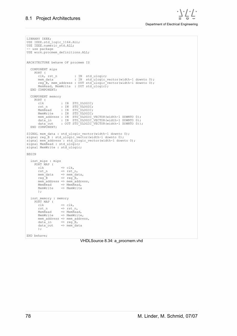
8.1 Project Architectures
LIBRARY IEEE;USE IEEE.std_logic_1164.ALL;USE IEEE.numeric_std.ALL;-- use packageUSE work.procmem_definitions.ALL;
ARCHITECTURE behave OF procmem IS COMPONENT mips PORT ( clk, rst_n : IN std_ulogic; mem_data : IN std_ulogic_vector(width-1 downto 0); reg_B, mem_address : OUT std_ulogic_vector(width-1 downto 0); MemRead, MemWrite : OUT std_ulogic); END COMPONENT; COMPONENT memory PORT ( clk : IN STD_ULOGIC; rst_n : IN STD_ULOGIC; MemRead : IN STD_ULOGIC; MemWrite : IN STD_ULOGIC; mem_address : IN STD_ULOGIC_VECTOR(width-1 DOWNTO 0); data_in : IN STD_ULOGIC_VECTOR(width-1 DOWNTO 0); data_out : OUT STD_ULOGIC_VECTOR(width-1 DOWNTO 0)); END COMPONENT; SIGNAL mem_data : std_ulogic_vector(width-1 downto 0);signal reg_B : std_ulogic_vector(width-1 downto 0);signal mem_address : std_ulogic_vector(width-1 downto 0);signal MemRead : std_ulogic;signal MemWrite : std_ulogic;BEGIN inst_mips : mips PORT MAP ( clk => clk, rst_n => rst_n, mem_data => mem_data, reg_B => reg_B, mem_address => mem_address, MemRead => MemRead, MemWrite => MemWrite ); inst_memory : memory PORT MAP ( clk => clk, rst_n => rst_n, MemRead => MemRead, MemWrite => MemWrite, mem_address => mem_address, data_in => reg_B, data_out => mem_data ); END behave;
VHDLSource 8.34: a_procmem.vhd
78 M. Linder, M. Schmid, 07/07
Department of Electrical Engineering

8.1 Package
8.1.3 Package
PACKAGE ProcMem_definitions IS -- globals CONSTANT width : NATURAL := 32; -- definitions for regfile CONSTANT regfile_depth : positive := 32; -- register file depth = 2**adrsize CONSTANT regfile_adrsize : positive := 5; -- address vector size = log2(depth) -- definitions for memory CONSTANT ram_adrwidth : positive := 8; -- m x n - RAM Block CONSTANT ram_datwidth : positive := 8; -- initial RAM content in IntelHEX Format CONSTANT ramfile_std : string := "./simulation/ram_256x8.hex"; CONSTANT ramfile_block0 : string := "./simulation/ram0_256x8.hex"; CONSTANT ramfile_block1 : string := "./simulation/ram1_256x8.hex"; CONSTANT ramfile_block2 : string := "./simulation/ram2_256x8.hex"; CONSTANT ramfile_block3 : string := "./simulation/ram3_256x8.hex"; END ProcMem_definitions;
VHDLSource 8.35: p_procmem_definitions.vhd
M. Linder, M. Schmid, 07/07 79
Department of Electrical Engineering

8.1 Testbenches
8.1.4 Testbenches
80 M. Linder, M. Schmid, 07/07
Department of Electrical Engineering

8.1 Testbenches
LIBRARY ieee;USE ieee.std_logic_1164.ALL;USE ieee.numeric_std.ALL;USE std.textio.ALL;USE ieee.std_logic_textio.ALL;-- use packageUSE work.procmem_definitions.ALL;-------------------------------------------------------------------------------ENTITY t_alu ISEND t_alu;-------------------------------------------------------------------------------ARCHITECTURE tbenchfileio OF t_alu IS -- component generics CONSTANT width : NATURAL := 32; COMPONENT alu PORT ( a, b : IN STD_ULOGIC_VECTOR(width-1 DOWNTO 0); opcode : IN STD_ULOGIC_VECTOR(2 DOWNTO 0); result : OUT STD_ULOGIC_VECTOR(width-1 DOWNTO 0); zero : OUT STD_ULOGIC); END COMPONENT; -- component ports SIGNAL a, b : STD_ULOGIC_VECTOR(width-1 DOWNTO 0); SIGNAL opcode : STD_ULOGIC_VECTOR(2 DOWNTO 0); SIGNAL result : STD_ULOGIC_VECTOR(width-1 DOWNTO 0); SIGNAL zero : STD_ULOGIC; -- definition of a clock period CONSTANT period : time := 10 ns; FUNCTION TO_string(arg : std_ulogic) RETURN string IS VARIABLE result_string : string(1 DOWNTO 1); BEGIN CASE arg IS WHEN 'U' => result_string(1) := 'U'; WHEN 'X' => result_string(1) := 'X'; WHEN '0' => result_string(1) := '0'; WHEN '1' => result_string(1) := '1'; WHEN 'Z' => result_string(1) := 'Z'; WHEN 'W' => result_string(1) := 'W'; WHEN 'L' => result_string(1) := 'L'; WHEN 'H' => result_string(1) := 'H'; WHEN '-' => result_string(1) := '-'; END CASE; RETURN result_string; END TO_string; FUNCTION TO_string(arg : unsigned) RETURN string IS ALIAS u : unsigned(arg'length DOWNTO 1) IS arg; VARIABLE result_string : string(arg'length DOWNTO 1); BEGIN FOR i IN u'range LOOP CASE u(i) IS WHEN 'U' => result_string(i) := 'U'; WHEN 'X' => result_string(i) := 'X'; WHEN '0' => result_string(i) := '0'; WHEN '1' => result_string(i) := '1'; WHEN 'Z' => result_string(i) := 'Z'; WHEN 'W' => result_string(i) := 'W'; WHEN 'L' => result_string(i) := 'L'; WHEN 'H' => result_string(i) := 'H'; WHEN '-' => result_string(i) := '-'; END CASE; END LOOP; RETURN result_string; END TO_string;BEGIN -- tbenchfileio
M. Linder, M. Schmid, 07/07 81
Department of Electrical Engineering

8.1 Testbenches
-- component instantiation DUT: alu PORT MAP ( a => a, b => b, opcode => opcode, result => result, zero => zero); stimuli_observer : PROCESS VARIABLE errflag : boolean := false; VARIABLE Li : line; -- pointer to file input buffer VARIABLE Lo : line; -- pointer to file output buffer FILE vectorfile : text OPEN read_mode IS "./stimuli/testpattern-ALU.in"; -- definition of input file structure: -- # comment line starts with hash character -- otherwise a space is required for the first character ! -- following definition of corresponding temp input buffer variables CONSTANT commentchar : character := '#'; -- comment character VARIABLE vectorfirstc : character := commentchar; -- first character VARIABLE vectornum : integer := 0; -- vector number VARIABLE vectordelimit : character := ' '; -- delimiter character between vectors -- variables used in file-io VARIABLE opcode_fio : STD_ULOGIC_VECTOR(2 DOWNTO 0); VARIABLE a_fio : INTEGER; VARIABLE b_fio : INTEGER; VARIABLE result_fio : INTEGER; VARIABLE zero_fio : STD_ULOGIC; BEGIN WHILE NOT endfile(vectorfile) LOOP -- read stimuli line by line readline(vectorfile, Li); IF (Li /= NULL) AND (Li'length > 0) THEN read(Li, vectorfirstc); IF (vectorfirstc /= commentchar) THEN read(Li, vectornum); read(Li, vectordelimit); -- read opcode read(Li, opcode_fio); opcode <= opcode_fio; -- read operand a read(Li, vectordelimit); read(Li, a_fio); a <= STD_ULOGIC_VECTOR(TO_UNSIGNED(a_fio, width)); -- read operand b read(Li, vectordelimit); read(Li, b_fio); b <= STD_ULOGIC_VECTOR(TO_UNSIGNED(b_fio, width)); -- read result read(Li, vectordelimit); read(Li, result_fio); -- read zero bit read(Li, vectordelimit); read(Li, zero_fio); WAIT FOR period; -- compare expected result IF result /= STD_ULOGIC_VECTOR(TO_UNSIGNED(result_fio, width)) THEN write(Lo, string'("Pattern No. ")); write(Lo, vectornum); writeline(OUTPUT, Lo); REPORT "Error: Wrong result!" & lf & to_string(UNSIGNED(result)) & " = result" & lf & to_string(TO_UNSIGNED(result_fio, width)) & " = expected result" & lf SEVERITY failure; errflag := true; END IF; -- compare zero-bit IF zero /= zero_fio THEN
82 M. Linder, M. Schmid, 07/07
Department of Electrical Engineering
8.1 Testbenches
write(Lo, string'("Pattern No. ")); write(Lo, vectornum); writeline(OUTPUT, Lo); REPORT "Error: Wrong zero-bit!" & lf & to_string(zero) & " = zero-bit" & lf & to_string(zero_fio) & " = expected zero-bit" SEVERITY failure; errflag := true; END IF; END IF; -- first character is a comment END IF; -- line is not null END LOOP; -- while not end of FILE ASSERT errflag REPORT "No errors !" SEVERITY note; WAIT; END PROCESS;END tbenchfileio;
VHDLSource 8.36: t_alu_fileio.vhd
M. Linder, M. Schmid, 07/07 83
Department of Electrical Engineering

8.1 Testbenches
LIBRARY ieee;USE ieee.std_logic_1164.ALL;USE IEEE.numeric_std.ALL;-- use packageUSE work.procmem_definitions.ALL;-------------------------------------------------------------------------------ENTITY t_memory ISEND t_memory;-------------------------------------------------------------------------------ARCHITECTURE tbench OF t_memory ISCOMPONENT memory IS PORT ( clk : IN STD_ULOGIC; rst_n : IN STD_ULOGIC; MemRead : IN STD_ULOGIC; MemWrite : IN STD_ULOGIC; mem_address : IN STD_ULOGIC_VECTOR(width-1 DOWNTO 0); data_in : IN STD_ULOGIC_VECTOR(width-1 DOWNTO 0); data_out : OUT STD_ULOGIC_VECTOR(width-1 DOWNTO 0) );END COMPONENT; -- component ports SIGNAL clk : STD_ULOGIC; SIGNAL rst_n : STD_ULOGIC; SIGNAL MemRead : STD_ULOGIC; SIGNAL MemWrite : STD_ULOGIC; SIGNAL mem_address : STD_ULOGIC_VECTOR(width-1 DOWNTO 0); SIGNAL data_in : STD_ULOGIC_VECTOR(width-1 DOWNTO 0); SIGNAL data_out : STD_ULOGIC_VECTOR(width-1 DOWNTO 0); -- definition of a clock period CONSTANT period : time := 10 ns; -- switch for clock generator SIGNAL clken_p : boolean := true; -- STD_ULOGIC_VECTOR TO STRING FUNCTION TO_string(arg : std_ulogic_vector) RETURN string IS ALIAS u : STD_ULOGIC_VECTOR(arg'length DOWNTO 1) IS arg; VARIABLE result : string(arg'length DOWNTO 1); BEGIN FOR i IN u'range LOOP CASE u(i) IS WHEN 'U' => result(i) := 'U'; WHEN 'X' => result(i) := 'X'; WHEN '0' => result(i) := '0'; WHEN '1' => result(i) := '1'; WHEN 'Z' => result(i) := 'Z'; WHEN 'W' => result(i) := 'W'; WHEN 'L' => result(i) := 'L'; WHEN 'H' => result(i) := 'H'; WHEN '-' => result(i) := '-'; END CASE; END LOOP; RETURN result; END TO_string; -- UNSIGNED TO STRING FUNCTION TO_string(arg : unsigned) RETURN string IS ALIAS u : unsigned(arg'length DOWNTO 1) IS arg; VARIABLE result : string(arg'length DOWNTO 1); BEGIN FOR i IN u'range LOOP CASE u(i) IS WHEN 'U' => result(i) := 'U'; WHEN 'X' => result(i) := 'X'; WHEN '0' => result(i) := '0'; WHEN '1' => result(i) := '1'; WHEN 'Z' => result(i) := 'Z'; WHEN 'W' => result(i) := 'W'; WHEN 'L' => result(i) := 'L'; WHEN 'H' => result(i) := 'H'; WHEN '-' => result(i) := '-';
84 M. Linder, M. Schmid, 07/07
Department of Electrical Engineering

8.1 Testbenches
END CASE; END LOOP; RETURN result; END TO_string;
BEGIN -- tbench -- component instantiation DUT: memory PORT MAP ( clk => clk, rst_n => rst_n, MemRead => MemRead, MemWrite => MemWrite, mem_address => mem_address, data_in => data_in, data_out => data_out ); -- clock generation clock_proc : PROCESS BEGIN WHILE clken_p LOOP clk <= '0'; WAIT FOR period/2; clk <= '1'; WAIT FOR period/2; END LOOP; WAIT; END PROCESS; -- reset generation reset : rst_n <= '0', '1' AFTER period;
-- waveform generation WaveGen_Proc : PROCESS VARIABLE mem_temp : STD_ULOGIC_VECTOR(width-1 DOWNTO 0); TYPE array_vector IS ARRAY (0 TO 5) OF STD_ULOGIC_VECTOR(width-1 DOWNTO 0); VARIABLE addr_pattern : array_vector; VARIABLE data_pattern : array_vector; BEGIN -- initialization MemRead <= '1'; MemWrite <= '0'; mem_address <= (OTHERS => '0'); -- addr_pattern addr_pattern := ( -- block: 3, 2, 1, 0 x"00000000", -- use correct word address x"00000004", x"00000008", x"0000000C", x"00000010", x"00000014"); data_pattern := ( -- data arises every byte x"01020304", x"05060708", x"090A0B0C", x"0D0E0F10", x"11121314", x"15161718"); -- reset WAIT FOR period; -- write pattern to mem MemRead <= '0'; MemWrite <= '1'; FOR i in data_pattern'RANGE LOOP data_in <= data_pattern(i); mem_address <= addr_pattern(i); WAIT FOR period; END LOOP; -- read memory and compare with pattern
M. Linder, M. Schmid, 07/07 85
Department of Electrical Engineering

8.1 Testbenches
MemRead <= '1'; MemWrite <= '0'; FOR k in data_pattern'RANGE LOOP mem_address <= addr_pattern(k); WAIT FOR period; ASSERT data_out = data_pattern(k) REPORT "p.no. " & TO_STRING(TO_UNSIGNED(k, data_pattern'LENGTH-1)) & lf & "act. address: " & lf & TO_STRING(mem_address) & lf & "actual value: " & lf & TO_STRING(data_out) & lf & "expected value: " & lf & TO_STRING(data_pattern(k)) SEVERITY note; END LOOP; WAIT FOR period; clken_p <= false; WAIT; END PROCESS WaveGen_Proc;END tbench;
VHDLSource 8.37: t_memory.vhd
86 M. Linder, M. Schmid, 07/07
Department of Electrical Engineering

8.1 Testbenches
LIBRARY ieee;USE ieee.std_logic_1164.ALL;USE IEEE.numeric_std.ALL;USE work.procmem_definitions.ALL;-------------------------------------------------------------------------------ENTITY t_procmem ISEND t_procmem;-------------------------------------------------------------------------------ARCHITECTURE tbench OF t_procmem ISCOMPONENT procmem IS PORT ( clk, rst_n : IN STD_ULOGIC );END COMPONENT; -- component ports SIGNAL clk : STD_ULOGIC; SIGNAL rst_n : STD_ULOGIC; -- definition of a clock period CONSTANT period : time := 10 ns; -- switch for clock generator SIGNAL clken_p : boolean := true; BEGIN -- tbench -- component instantiation DUT: procmem PORT MAP ( clk => clk, rst_n => rst_n ); -- clock generation clock_proc : PROCESS BEGIN WHILE clken_p LOOP clk <= '0'; WAIT FOR period/2; clk <= '1'; WAIT FOR period/2; END LOOP; WAIT; END PROCESS; -- reset generation reset : rst_n <= '0', '1' AFTER period; -- waveform generation WaveGen_Proc : PROCESS BEGIN -- reset WAIT FOR period; -- wait for results WAIT FOR 25*period; clken_p <= false; WAIT; END PROCESS WaveGen_Proc;END tbench;
VHDLSource 8.38: t_procmem.vhd
M. Linder, M. Schmid, 07/07 87
Department of Electrical Engineering

8.1 Testbenches
LIBRARY ieee;USE ieee.std_logic_1164.ALL;USE IEEE.numeric_std.ALL;-- use packageUSE work.procmem_definitions.ALL;-------------------------------------------------------------------------------ENTITY t_procmem_init ISEND t_procmem_init;-------------------------------------------------------------------------------ARCHITECTURE tbench OF t_procmem_init IS COMPONENT mips PORT ( clk, rst_n : IN std_ulogic; mem_data : IN std_ulogic_vector(width-1 downto 0); reg_B, mem_address : OUT std_ulogic_vector(width-1 downto 0); MemRead, MemWrite : OUT std_ulogic); END COMPONENT; COMPONENT memory PORT ( clk : IN STD_ULOGIC; rst_n : IN STD_ULOGIC; MemRead : IN STD_ULOGIC; MemWrite : IN STD_ULOGIC; mem_address : IN STD_ULOGIC_VECTOR(width-1 DOWNTO 0); data_in : IN STD_ULOGIC_VECTOR(width-1 DOWNTO 0); data_out : OUT STD_ULOGIC_VECTOR(width-1 DOWNTO 0)); END COMPONENT; -- component ports SIGNAL clk : STD_ULOGIC; SIGNAL rst_n : STD_ULOGIC; SIGNAL mem_data : std_ulogic_vector(width-1 downto 0); signal reg_B : std_ulogic_vector(width-1 downto 0); signal mem_address : std_ulogic_vector(width-1 downto 0); signal MemRead : std_ulogic; signal MemWrite : std_ulogic; SIGNAL mem_data_ini : std_ulogic_vector(width-1 downto 0); signal reg_B_ini : std_ulogic_vector(width-1 downto 0); signal mem_address_ini : std_ulogic_vector(width-1 downto 0); signal MemRead_ini : std_ulogic; signal MemWrite_ini : std_ulogic; SIGNAL mem_data_mux : std_ulogic_vector(width-1 downto 0); signal reg_B_mux : std_ulogic_vector(width-1 downto 0); signal mem_address_mux : std_ulogic_vector(width-1 downto 0); signal MemRead_mux : std_ulogic; signal MemWrite_mux : std_ulogic; -- definition of a clock period CONSTANT period : time := 10 ns; -- switch for clock generator SIGNAL clken_p : boolean := true; BEGIN -- tbench inst_mips : mips PORT MAP ( clk => clk, rst_n => rst_n, mem_data => mem_data_mux, reg_B => reg_B, mem_address => mem_address, MemRead => MemRead, MemWrite => MemWrite ); inst_memory : memory
88 M. Linder, M. Schmid, 07/07
Department of Electrical Engineering

8.1 Testbenches
PORT MAP ( clk => clk, rst_n => rst_n, MemRead => MemRead_mux, MemWrite => MemWrite_mux, mem_address => mem_address_mux, data_in => reg_B_mux, data_out => mem_data ); -- clock generation clock_proc : PROCESS BEGIN WHILE clken_p LOOP clk <= '0'; WAIT FOR period/2; clk <= '1'; WAIT FOR period/2; END LOOP; WAIT; END PROCESS; -- reset generation -- not used because of initialisation during explicit reset --reset : rst_n <= '0', '1' AFTER period; -- multiplexer for memory initialization signals, -- because there is only one driver allowed at each signal mux : PROCESS(rst_n, MemWrite_ini, MemRead_ini, mem_data_ini, reg_B_ini, mem_address_ini, MemWrite, MemRead, mem_data, reg_B, mem_address) BEGIN IF rst_n = '0' THEN MemWrite_mux <= MemWrite_ini; MemRead_mux <= MemRead_ini; mem_data_mux <= mem_data_ini; reg_B_mux <= reg_B_ini; mem_address_mux <= mem_address_ini; ELSE MemWrite_mux <= MemWrite; MemRead_mux <= MemRead; mem_data_mux <= mem_data; reg_B_mux <= reg_B; mem_address_mux <= mem_address; END IF; END PROCESS; -- waveform generation WaveGen_Proc : PROCESS VARIABLE mem_temp : STD_ULOGIC_VECTOR(width-1 DOWNTO 0); TYPE array_vector IS ARRAY (0 TO 15) OF STD_ULOGIC_VECTOR(width-1 DOWNTO 0); VARIABLE addr_pattern : array_vector; VARIABLE data_pattern : array_vector; BEGIN -- pattern needed for memory initialisation at the beginning addr_pattern := ( x"00000000", x"00000004", x"00000008", x"0000000C", x"00000010", x"00000014", x"00000018", x"0000001C", x"00000020", x"00000024", x"00000028", x"0000002C", x"00000030", x"00000038", x"00000080", x"00000084" ); data_pattern := (
M. Linder, M. Schmid, 07/07 89
Department of Electrical Engineering

8.1 Testbenches
"10001100000100000000000010000000", "10001100000100010000000010000100", "00000010000100011001000000100000", "10101100000100100000000010001000", "00000010001100001001100000100010", "10101100000100110000000010001100", "00000010001100001010000000100100", "10101100000101000000000010010000", "00000010001100001010100000100101", "10101100000101010000000010010100", "00000010000100011011000000101010", "10101100000101100000000010011000", "00010010000101000000000000000001", "00001000000000000000000000000010", "00000000000000000000000101111011", "00000000000000000000000101111111"); -- explicit reset rst_n <= '0'; -- initialize memory output mem_data_ini <= (OTHERS => '0'); -- write pattern to mem MemWrite_ini <= '1'; MemRead_ini <= '0'; FOR i in data_pattern'RANGE LOOP reg_B_ini <= data_pattern(i); mem_address_ini <= addr_pattern(i); WAIT FOR period; END LOOP; -- set signals to zero before quitting initialisation WAIT FOR period; MemWrite_ini <= '0'; MemRead_ini <= '0'; reg_B_ini <= (OTHERS => '0'); mem_address_ini <= (OTHERS => '0'); mem_data_ini <= (OTHERS => '0'); WAIT FOR 2*period; -- start rst_n <= '1'; -- wait for results WAIT FOR 100*period; clken_p <= false; WAIT; END PROCESS WaveGen_Proc;
END tbench;
90 M. Linder, M. Schmid, 07/07
Department of Electrical Engineering

8.2 References
8.2 References
[PaHe98]: David A. Patterson, John L. Hennessy:
„Computer Organization and Design - The Hardware/Software
Interface“
Second Editon (1998)
Morgan Kaufmann Publisher, Inc.
es_cycii.pdf Altera Corporation
Cyclone II FPGA Family Erata Sheet ES-030405-1.3
www.altera.com
vhdl_course.pdf Alfred Eder:
„VHDL Short Course & Guide to Synthesizable Code“
Version 03/2004
www.fh-augsburg.de
M. Linder, M. Schmid, 07/07 91
Department of Electrical Engineering
Related Documents