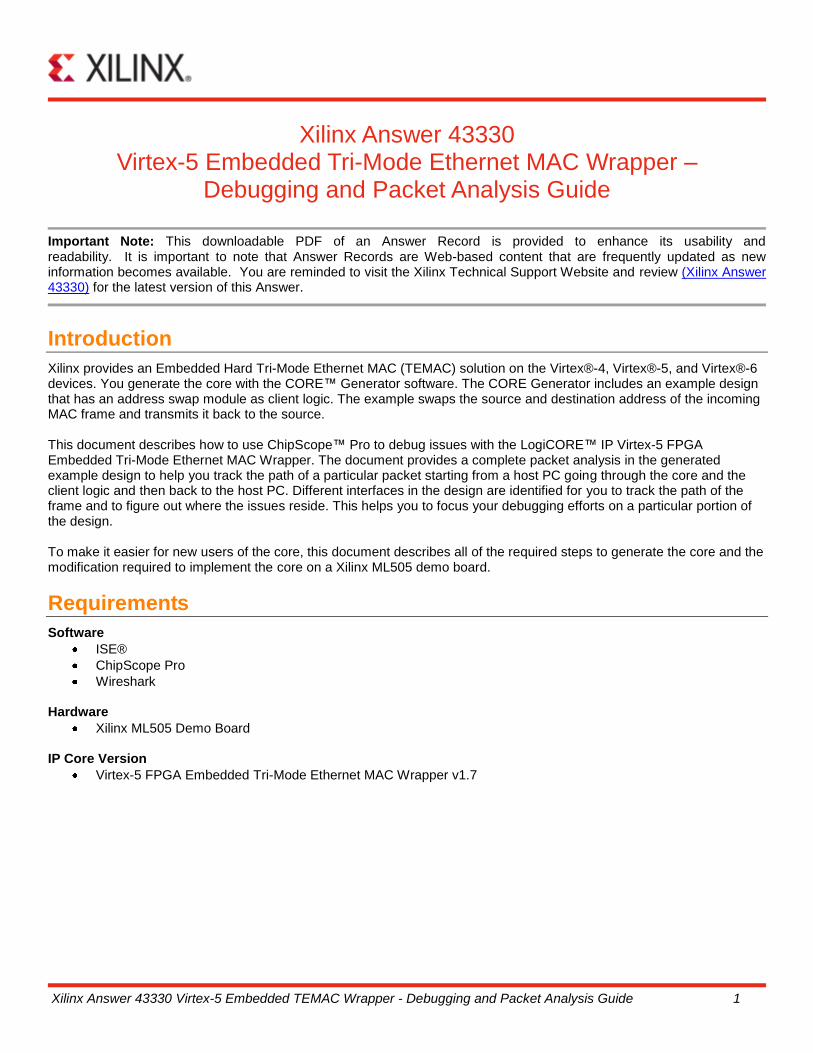
Xilinx Answer 43330 Virtex-5 Embedded TEMAC Wrapper - Debugging and Packet Analysis Guide 1 Xilinx Answer 43330 Virtex-5 Embedded Tri-Mode Ethernet MAC Wrapper – Debugging and Packet Analysis Guide Important Note: This downloadable PDF of an Answer Record is provided to enhance its usability and readability. It is important to note that Answer Records are Web-based content that are frequently updated as new information becomes available. You are reminded to visit the Xilinx Technical Support Website and review (Xilinx Answer 43330) for the latest version of this Answer. Introduction Xilinx provides an Embedded Hard Tri-Mode Ethernet MAC (TEMAC) solution on the Virtex®-4, Virtex®-5, and Virtex®-6 devices. You generate the core with the CORE™ Generator software. The CORE Generator includes an example design that has an address swap module as client logic. The example swaps the source and destination address of the incoming MAC frame and transmits it back to the source. This document describes how to use ChipScope™ Pro to debug issues with the LogiCORE™ IP Virtex-5 FPGA Embedded Tri-Mode Ethernet MAC Wrapper. The document provides a complete packet analysis in the generated example design to help you track the path of a particular packet starting from a host PC going through the core and the client logic and then back to the host PC. Different interfaces in the design are identified for you to track the path of the frame and to figure out where the issues reside. This helps you to focus your debugging efforts on a particular portion of the design. To make it easier for new users of the core, this document describes all of the required steps to generate the core and the modification required to implement the core on a Xilinx ML505 demo board. Requirements Software ISE® ChipScope Pro Wireshark Hardware Xilinx ML505 Demo Board IP Core Version Virtex-5 FPGA Embedded Tri-Mode Ethernet MAC Wrapper v1.7

Welcome message from author
This document is posted to help you gain knowledge. Please leave a comment to let me know what you think about it! Share it to your friends and learn new things together.
Transcript
Xilinx Answer 43330 Virtex-5 Embedded TEMAC Wrapper - Debugging and Packet Analysis Guide 1
Xilinx Answer 43330 Virtex-5 Embedded Tri-Mode Ethernet MAC Wrapper –
Debugging and Packet Analysis Guide
Important Note: This downloadable PDF of an Answer Record is provided to enhance its usability and readability. It is important to note that Answer Records are Web-based content that are frequently updated as new information becomes available. You are reminded to visit the Xilinx Technical Support Website and review (Xilinx Answer 43330) for the latest version of this Answer.
Introduction
Xilinx provides an Embedded Hard Tri-Mode Ethernet MAC (TEMAC) solution on the Virtex®-4, Virtex®-5, and Virtex®-6 devices. You generate the core with the CORE™ Generator software. The CORE Generator includes an example design that has an address swap module as client logic. The example swaps the source and destination address of the incoming MAC frame and transmits it back to the source. This document describes how to use ChipScope™ Pro to debug issues with the LogiCORE™ IP Virtex-5 FPGA Embedded Tri-Mode Ethernet MAC Wrapper. The document provides a complete packet analysis in the generated example design to help you track the path of a particular packet starting from a host PC going through the core and the client logic and then back to the host PC. Different interfaces in the design are identified for you to track the path of the frame and to figure out where the issues reside. This helps you to focus your debugging efforts on a particular portion of the design. To make it easier for new users of the core, this document describes all of the required steps to generate the core and the modification required to implement the core on a Xilinx ML505 demo board.
Requirements
Software
ISE®
ChipScope Pro
Wireshark Hardware
Xilinx ML505 Demo Board IP Core Version
Virtex-5 FPGA Embedded Tri-Mode Ethernet MAC Wrapper v1.7
Xilinx Answer 43330 Virtex-5 Embedded TEMAC Wrapper - Debugging and Packet Analysis Guide 2
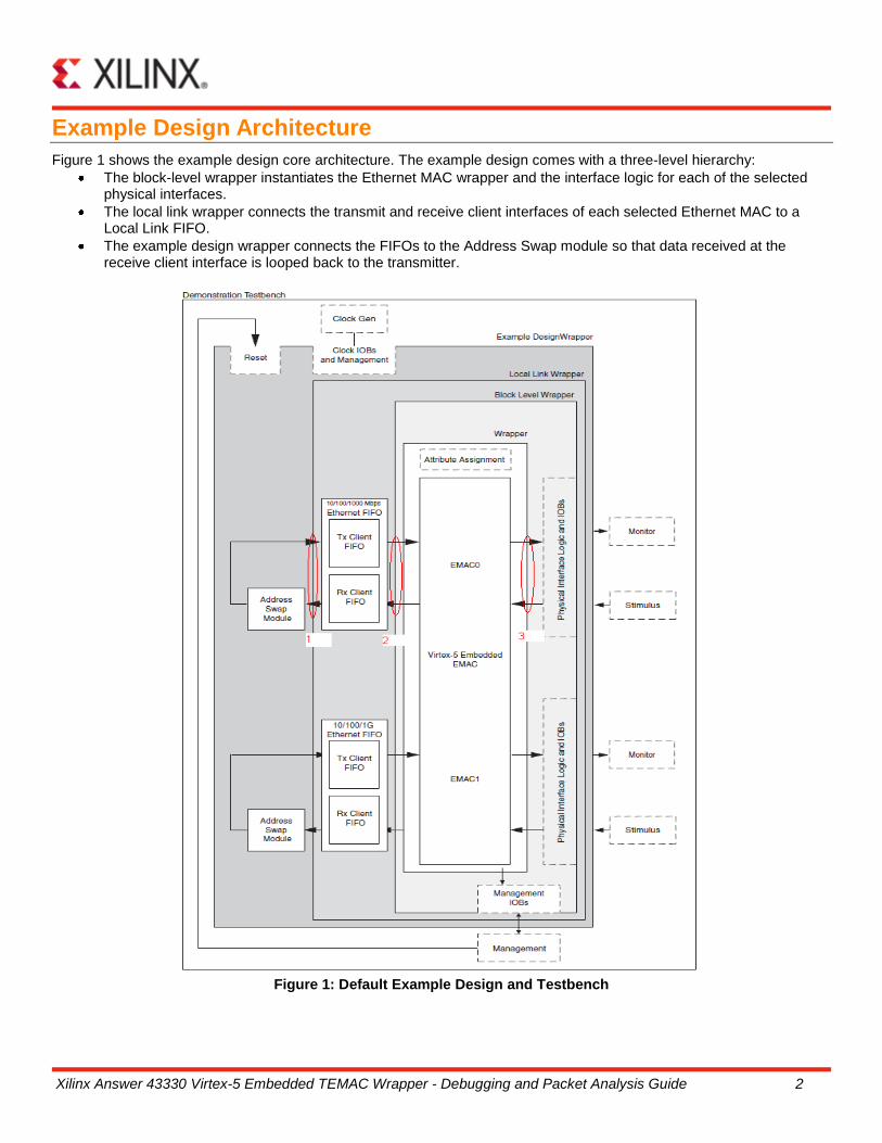
Example Design Architecture
Figure 1 shows the example design core architecture. The example design comes with a three-level hierarchy:
The block-level wrapper instantiates the Ethernet MAC wrapper and the interface logic for each of the selected physical interfaces.
The local link wrapper connects the transmit and receive client interfaces of each selected Ethernet MAC to a Local Link FIFO.
The example design wrapper connects the FIFOs to the Address Swap module so that data received at the receive client interface is looped back to the transmitter.
Figure 1: Default Example Design and Testbench

Xilinx Answer 43330 Virtex-5 Embedded TEMAC Wrapper - Debugging and Packet Analysis Guide 3
The Address Swap module represents the back-end client logic user application. To implement your own design, you replace this module with your design. The Address Swap module swaps the source and destination addresses of the incoming frame. Using this method, frames received from a link partner, for example, a protocol tester or a host PC, are relayed back to the source.
Example Design Interfaces
This section describes each interface in the SGMII example design. The main idea for identifying these interfaces is to track the path of the packet. If the design is not working, for example, a packet transmitted from the core to the link partner is not received, it is recommended that you probe each of these interfaces step-by-step and make sure that the packet appears correctly in these interfaces. There are six different interfaces that you can use to probe for debugging purposes as follows:
1. RX Physical (GTP) Interface [Interface-3 in Figure 1] 2. TX Physical (GTP) Interface [Interface-3 in Figure 1] 3. RX MAC Client Interface [Interface-2 in Figure 1] 4. TX MAC Client Interface [Interface-2 in Figure 1] 5. RX Local Link Interface [Interface-1 in Figure 1] 6. TX Local Link Interface [Interface-1 in Figure 1]
The next sections list the signals at each interface in the SGMII example design.
RX Physical (GTP) Interface
This section lists the signals that can be probed in ChipScope Pro to debug issues related to the RX Physical (GTP) interface.
RESETDONE
ENMCOMMAALIGN
ENPCOMMAALIGN
LOOPBACK
POWERDOWN
RXUSRCLK
This section lists the signals that can be probed in ChipScope Pro to debug issues related to the RXUSRCLK interface.
RXUSRCLK2
RXRESET
TXCHARDISPMODE
TXCHARDISPVAL
TXCHARISK
TXDATA
TXUSRCLK
TXUSRCLK2
TXRESET
RXCHARISCOMMA
RXCHARISK
RXCLKCORCNT
RXDATA
RXDISPERR
RXNOTINTABLE
RXRUNDISP
RXBUFERR
TXBUFERR

Xilinx Answer 43330 Virtex-5 Embedded TEMAC Wrapper - Debugging and Packet Analysis Guide 4
PLLLKDET
TXOUTCLK
RXELECIDLE
GTRESET
PMARESET
DCM_LOCKED
RX MAC Client Interface
This section lists the signals that can be probed in ChipScope Pro to debug issues related to the RX MAC Client Interface.
EMAC#CLIENTRXCLIENTCLKOUT
CLIENTEMAC#RXCLIENTCLKIN
EMAC#CLIENTRXD
EMAC#CLIENTRXDVLD
EMAC#CLIENTRXDVLDMSW
EMAC#CLIENTRXGOODFRAME
EMAC#CLIENTRXBADFRAME
EMAC#CLIENTRXFRAMEDROP
EMAC#CLIENTRXSTATS
EMAC#CLIENTRXSTATSVLD
EMAC#CLIENTRXSTATSBYTEVLD
TX MAC Client Interface
This section lists the signals that can be probed in ChipScope Pro to debug issues related to the TX MAC Client Interface.
EMAC#CLIENTTXCLIENTCLKOUT
CLIENTEMAC#TXCLIENTCLKIN
CLIENTEMAC#TXD
CLIENTEMAC#TXDVLD
CLIENTEMAC#TXDVLDMSW
EMAC#CLIENTTXACK
CLIENTEMAC#TXFIRSTBYTE
CLIENTEMAC#TXUNDERRUN
EMAC#CLIENTTXCOLLISION
EMAC#CLIENTTXRETRANSMIT
CLIENTEMAC#TXIFGDELAY
EMAC#CLIENTTXSTATS
EMAC#CLIENTTXSTATSVLD
EMAC#CLIENTTXSTATSBYTEVLD
RX Local Link Interface
This section lists the signals that can be probed in ChipScope Pro to debug issues related to the RX Local Link Interface.
RX_LL_CLOCK_#
RX_LL_RESET_#
RX_LL_DATA_#
RX_LL_SOF_N_#
RX_LL_EOF_N_#
RX_LL_SRC_RDY_N_#
RX_LL_DST_RDY_N_#
RX_LL_FIFO_STATUS_#
Xilinx Answer 43330 Virtex-5 Embedded TEMAC Wrapper - Debugging and Packet Analysis Guide 5
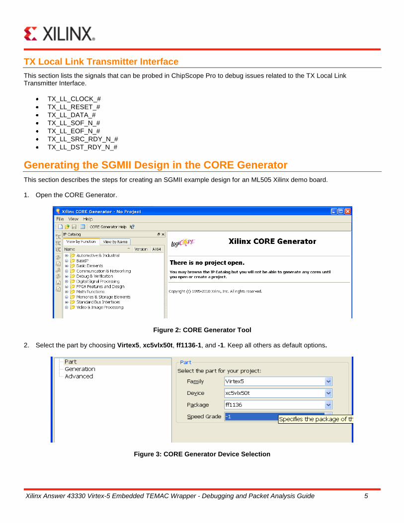
TX Local Link Transmitter Interface
This section lists the signals that can be probed in ChipScope Pro to debug issues related to the TX Local Link Transmitter Interface.
TX_LL_CLOCK_#
TX_LL_RESET_#
TX_LL_DATA_#
TX_LL_SOF_N_#
TX_LL_EOF_N_#
TX_LL_SRC_RDY_N_#
TX_LL_DST_RDY_N_#
Generating the SGMII Design in the CORE Generator
This section describes the steps for creating an SGMII example design for an ML505 Xilinx demo board. 1. Open the CORE Generator.
Figure 2: CORE Generator Tool 2. Select the part by choosing Virtex5, xc5vlx50t, ff1136-1, and -1. Keep all others as default options.
Figure 3: CORE Generator Device Selection

Xilinx Answer 43330 Virtex-5 Embedded TEMAC Wrapper - Debugging and Packet Analysis Guide 6
3. Double click Virtex-5 Embedded Tri- Mode Ethernet MAC Wrapper 1.7.
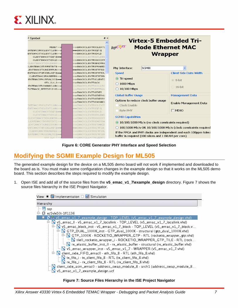
Figure 4: CORE Generator Core Selection 4. Configure the Virtex-5 Embedded Tri-Mode Ethernet MAC Wrapper as follows and generate the core.
Host Type – None
Enable Emacs – Only Enable Emac 0
PHY Interface – SGMII
Speed – Tri-speed
SGMII Capabilities – 10/100/1000 Mb/s (no clock constraints required)
Flow Control Configuration – Enable Rx and Tx Flow Control Figure 5 and Figure 6 show the CORE Generator selections.
Figure 5: CORE Generator Host Type Selection
Xilinx Answer 43330 Virtex-5 Embedded TEMAC Wrapper - Debugging and Packet Analysis Guide 7
Figure 6: CORE Generator PHY Interface and Speed Selection
Modifying the SGMII Example Design for ML505
The generated example design for the device on a ML505 demo board will not work if implemented and downloaded to the board as is. You must make some configuration changes in the example design so that it works on the ML505 demo board. This section describes the steps required to modify the example design. 1. Open ISE and add all of the source files from the v5_emac_v1_7\example_design directory. Figure 7 shows the
source files hierarchy in the ISE Project Navigator.
Figure 7: Source Files Hierarchy in the ISE Project Navigator

Xilinx Answer 43330 Virtex-5 Embedded TEMAC Wrapper - Debugging and Packet Analysis Guide 8
2. Modify the example design as follows:
a) Add PHY_RESET as an output port in the top level file. This is the signal connected to the reset input of the PHY.
The reset signal is active low. Connect the port as follows:
PHY_RESET <= not reset_i;
b) Add following in the top level, the PHY address for phy0 is 7.
signal PHYAD_0_int: std_logic_vector (4 downto 0) := "00111";
signal CLIENTEMAC0PAUSEREQ_int: std_logic := '0';
signal CLIENTEMAC0PAUSEVAL_int: std_logic_vector (15 downto 0) := x"0000";
signal CLIENTEMAC0TXIFGDELAY_int:std_logic_vector(7 downto 0):=(others=>'0');
c) Comment out all of the following from the top level and put 'open' in the corresponding output ports of the module
instantiation. --Client Receiver Interface - EMAC0
-- EMAC0CLIENTRXDVLD: out std_logic;
-- EMAC0CLIENTRXFRAMEDROP: out std_logic;
-- EMAC0CLIENTRXSTATS : out std_logic_vector(6 downto 0);
-- EMAC0CLIENTRXSTATSVLD: out std_logic;
-- EMAC0CLIENTRXSTATSBYTEVLD: out std_logic;
--Client Transmitter Interface - EMAC0
-- CLIENTEMAC0TXIFGDELAY : in std_logic_vector(7 downto 0);
-- EMAC0CLIENTTXSTATS : out std_logic;
-- EMAC0CLIENTTXSTATSVLD: out std_logic;
-- EMAC0CLIENTTXSTATSBYTEVLD: out std_logic;
--MAC Control Interface - EMAC0
-- CLIENTEMAC0PAUSEREQ: in std_logic;
-- CLIENTEMAC0PAUSEVAL: in std_logic_vector(15 downto 0);
--EMAC-MGT link status
-- EMAC0CLIENTSYNCACQSTATUS: out std_logic;
--EMAC0 Interrupt
-- EMAC0ANINTERRUPT: out std_logic;
3. In the v5_emac_v1_7.vhd file, change the following line:
constant EMAC0_PHYINITAUTONEG_ENABLE : boolean := TRUE;
-- FALSE by default
4. Modify the UCF file as follows:
INST"*GTX_DUAL_1000X_inst?GTX_1000X?tile0_rocketio_wrapper_gtx_i?gtx_dual_i" LOC =
"GTP_DUAL_X0Y3"; # for ML505 SGMII
INST "MGTCLK_N" LOC = "P3"; INST "MGTCLK_P" LOC = "P4";
5. Add the following lines in the UCF file. U8 is connected to a push button on the board. J14 is connected to the PHY
reset port: NET "RESET" LOC = "U8";
NET "PHY_RESET" LOC = "J14";
Xilinx Answer 43330 Virtex-5 Embedded TEMAC Wrapper - Debugging and Packet Analysis Guide 9
6. Implement the design in ISE to generate the bit stream.
Testing the Example Design
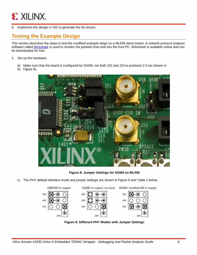
This section describes the steps to test the modified example deign on a ML505 demo board. A network protocol analyzer software called Wireshark is used to monitor the packets from and into the host PC. Wireshark is available online and can be downloaded for free. 1. Set up the hardware.
a) Make sure that the board is configured for SGMII: set both J22 and J23 to positions 2-3 (as shown in b) Figure 8).
Figure 8: Jumper Settings for SGMII on ML505
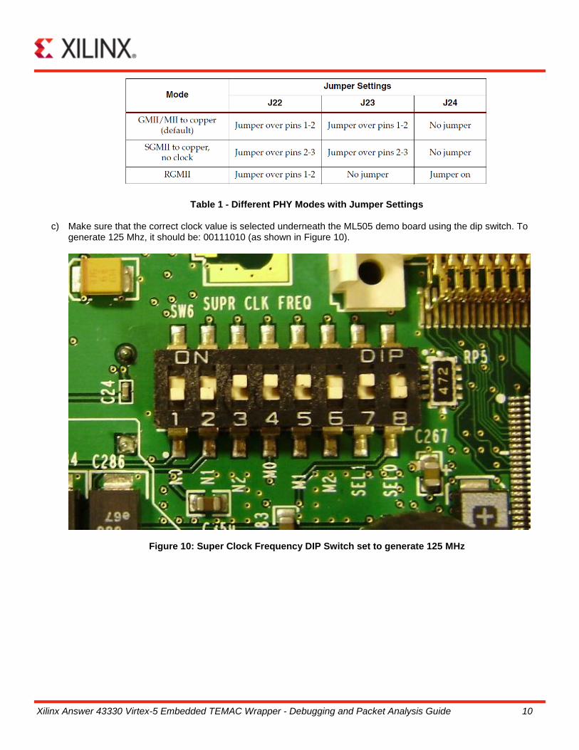
c) The PHY default interface mode and jumper settings are shown in Figure 9 and Table 1 below.
Figure 9: Different PHY Modes with Jumper Settings
Xilinx Answer 43330 Virtex-5 Embedded TEMAC Wrapper - Debugging and Packet Analysis Guide 10
Table 1 - Different PHY Modes with Jumper Settings
c) Make sure that the correct clock value is selected underneath the ML505 demo board using the dip switch. To generate 125 Mhz, it should be: 00111010 (as shown in Figure 10).
Figure 10: Super Clock Frequency DIP Switch set to generate 125 MHz

Xilinx Answer 43330 Virtex-5 Embedded TEMAC Wrapper - Debugging and Packet Analysis Guide 11
Table 2 shows the DIP switch table for the Super Clock frequency (SW6).
Table 2 - Super Clock Frequency DIP Switch (SW6) 2. Set up the Network.
a) In the Network Connection, right click on the Ethernet Adapter and select Properties. Set your host PC to the IP
address as shown in Figure 11.
Figure 11: IP Address Setup
b) In the Network Connection, right click on the Ethernet Adapter and select Properties; and then click Configure.

Xilinx Answer 43330 Virtex-5 Embedded TEMAC Wrapper - Debugging and Packet Analysis Guide 12
3. In the Advanced tab, set the Flow Control to Auto.
Figure 12: Flow Control Setup
a) Set Speed & Duplex to Auto.
Figure 13: Speed & Duplex Setup

Xilinx Answer 43330 Virtex-5 Embedded TEMAC Wrapper - Debugging and Packet Analysis Guide 13
4. Connect an Ethernet cable from the ML505 demo board to the Gigabit Ethernet Adapter.
Figure 14: Ethernet Cable Connection with PC For the detailed SGMII schematics on the ML505 demo board, see the PDF referenced below. http://www.xilinx.com/support/documentation/boards_and_kits/ml50x_schematics.pdf. 5. Download the bitstream using iMPACT on the ML505 demo board. 6. Capture the packets in Wireshark.
a) Open a command shell. b) Type: arp –s 1.2.3.5 00-0a-35-01-93-40
This arp command associates an IP Address with an Ethernet MAC Address.
Figure 15: Command to Associate an IP Address with a MAC Address

Xilinx Answer 43330 Virtex-5 Embedded TEMAC Wrapper - Debugging and Packet Analysis Guide 14
7. Start Wireshark.
a) Select Capture > Options… b) Select the Gigabit adapter on your computer as the interface and deselect Display Options. c) Click Start.
Figure 16: Wireshark Capture Options
d) In the command shell, type: ping –w 1 –n 1 1.2.3.5 and allow it to time out.
Figure 17: The ping Command
Xilinx Answer 43330 Virtex-5 Embedded TEMAC Wrapper - Debugging and Packet Analysis Guide 15
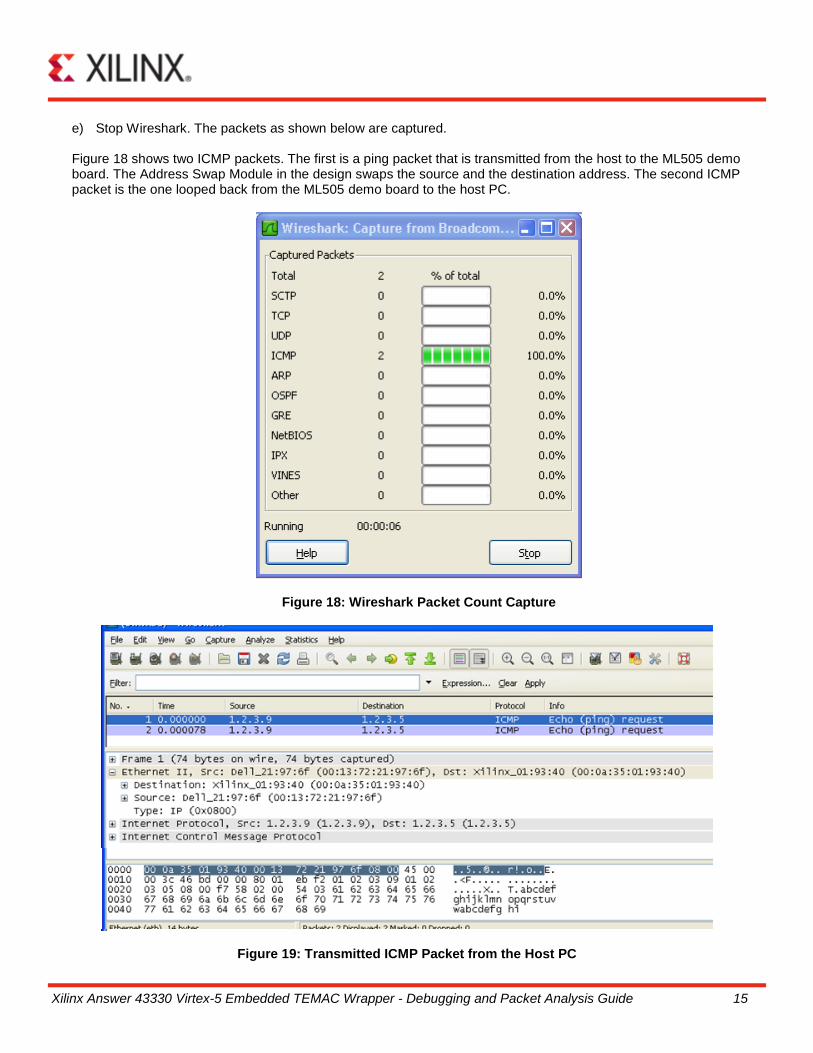
e) Stop Wireshark. The packets as shown below are captured.
Figure 18 shows two ICMP packets. The first is a ping packet that is transmitted from the host to the ML505 demo board. The Address Swap Module in the design swaps the source and the destination address. The second ICMP packet is the one looped back from the ML505 demo board to the host PC.
Figure 18: Wireshark Packet Count Capture
Figure 19: Transmitted ICMP Packet from the Host PC
Xilinx Answer 43330 Virtex-5 Embedded TEMAC Wrapper - Debugging and Packet Analysis Guide 16
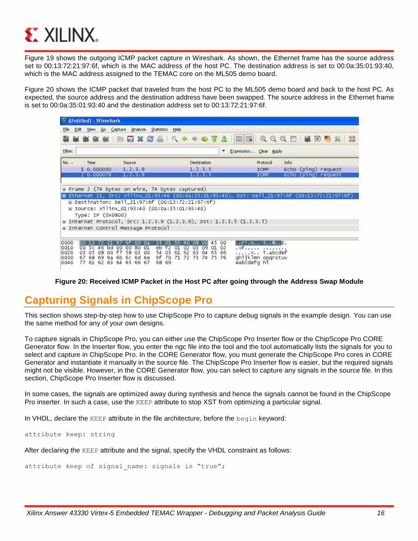
Figure 19 shows the outgoing ICMP packet capture in Wireshark. As shown, the Ethernet frame has the source address set to 00:13:72:21:97:6f, which is the MAC address of the host PC. The destination address is set to 00:0a:35:01:93:40, which is the MAC address assigned to the TEMAC core on the ML505 demo board. Figure 20 shows the ICMP packet that traveled from the host PC to the ML505 demo board and back to the host PC. As expected, the source address and the destination address have been swapped. The source address in the Ethernet frame is set to 00:0a:35:01:93:40 and the destination address set to 00:13:72:21:97:6f.
Figure 20: Received ICMP Packet in the Host PC after going through the Address Swap Module
Capturing Signals in ChipScope Pro
This section shows step-by-step how to use ChipScope Pro to capture debug signals in the example design. You can use the same method for any of your own designs. To capture signals in ChipScope Pro, you can either use the ChipScope Pro Inserter flow or the ChipScope Pro CORE Generator flow. In the Inserter flow, you enter the ngc file into the tool and the tool automatically lists the signals for you to select and capture in ChipScope Pro. In the CORE Generator flow, you must generate the ChipScope Pro cores in CORE Generator and instantiate it manually in the source file. The ChipScope Pro Inserter flow is easier, but the required signals might not be visible. However, in the CORE Generator flow, you can select to capture any signals in the source file. In this section, ChipScope Pro Inserter flow is discussed. In some cases, the signals are optimized away during synthesis and hence the signals cannot be found in the ChipScope
Pro inserter. In such a case, use the KEEP attribute to stop XST from optimizing a particular signal.
In VHDL, declare the KEEP attribute in the file architecture, before the begin keyword:
attribute keep: string
After declaring the KEEP attribute and the signal, specify the VHDL constraint as follows:
attribute keep of signal_name: signals is “true”;
Xilinx Answer 43330 Virtex-5 Embedded TEMAC Wrapper - Debugging and Packet Analysis Guide 17
In Verilog, add following:
(* KEEP = "{TRUE}" *) wire signal_name;
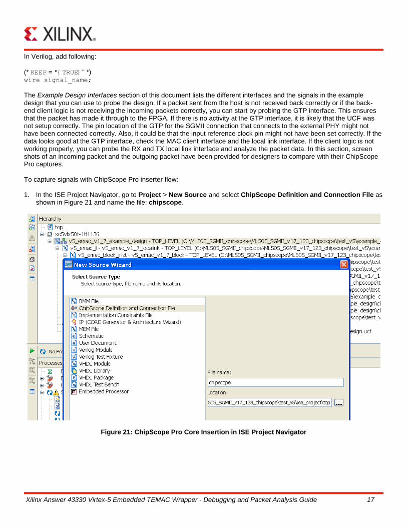
The Example Design Interfaces section of this document lists the different interfaces and the signals in the example design that you can use to probe the design. If a packet sent from the host is not received back correctly or if the back-end client logic is not receiving the incoming packets correctly, you can start by probing the GTP interface. This ensures that the packet has made it through to the FPGA. If there is no activity at the GTP interface, it is likely that the UCF was not setup correctly. The pin location of the GTP for the SGMII connection that connects to the external PHY might not have been connected correctly. Also, it could be that the input reference clock pin might not have been set correctly. If the data looks good at the GTP interface, check the MAC client interface and the local link interface. If the client logic is not working properly, you can probe the RX and TX local link interface and analyze the packet data. In this section, screen shots of an incoming packet and the outgoing packet have been provided for designers to compare with their ChipScope Pro captures. To capture signals with ChipScope Pro inserter flow: 1. In the ISE Project Navigator, go to Project > New Source and select ChipScope Definition and Connection File as
shown in Figure 21 and name the file: chipscope.
Figure 21: ChipScope Pro Core Insertion in ISE Project Navigator

Xilinx Answer 43330 Virtex-5 Embedded TEMAC Wrapper - Debugging and Packet Analysis Guide 18
After completing step 1, the CDC file appears in the sources window hierarchy as shown in Figure 22. The CDC file is the project file for ChipScope Pro Inserter.
Figure 22: ChipScope CDC file in Source Window in ISE Project Navigator 2. Double click on the CDC file. By doing so, the ChipScope Pro Core Inserter opens as shown in Figure 23.
Figure 23: ChipScope Pro Core Inserter

Xilinx Answer 43330 Virtex-5 Embedded TEMAC Wrapper - Debugging and Packet Analysis Guide 19
3. Click Next and then click New ILA Unit.
Figure 24: Add New ChipScope ILA 4. Change the settings as shown in Figure 25.
Figure 25: Change Trigger Parameters Options
Xilinx Answer 43330 Virtex-5 Embedded TEMAC Wrapper - Debugging and Packet Analysis Guide 20
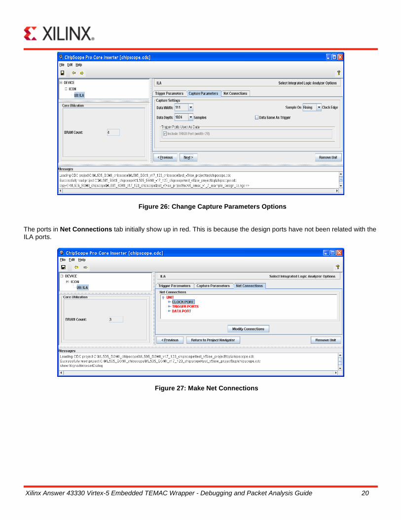
Figure 26: Change Capture Parameters Options The ports in Net Connections tab initially show up in red. This is because the design ports have not been related with the ILA ports.
Figure 27: Make Net Connections
Xilinx Answer 43330 Virtex-5 Embedded TEMAC Wrapper - Debugging and Packet Analysis Guide 21
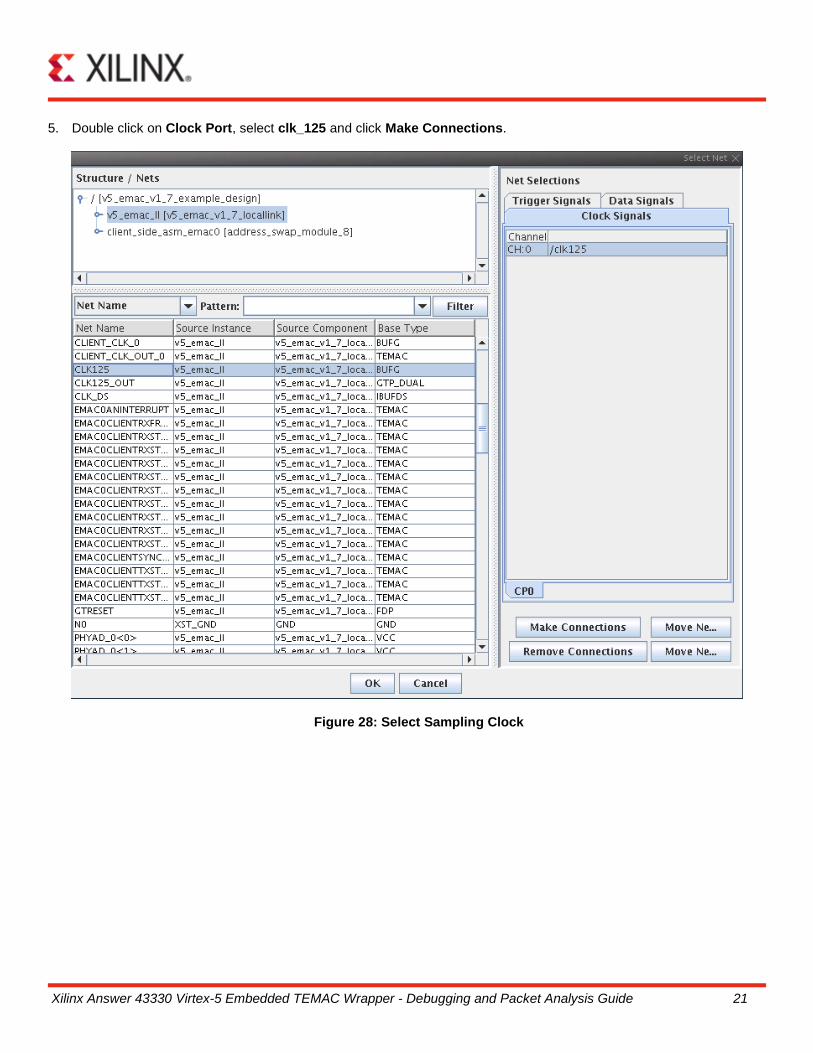
5. Double click on Clock Port, select clk_125 and click Make Connections.
Figure 28: Select Sampling Clock
Xilinx Answer 43330 Virtex-5 Embedded TEMAC Wrapper - Debugging and Packet Analysis Guide 22
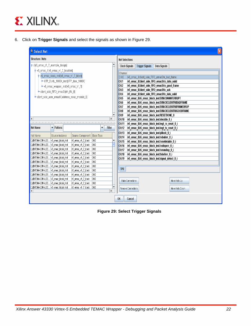
6. Click on Trigger Signals and select the signals as shown in Figure 29.
Figure 29: Select Trigger Signals
Xilinx Answer 43330 Virtex-5 Embedded TEMAC Wrapper - Debugging and Packet Analysis Guide 23
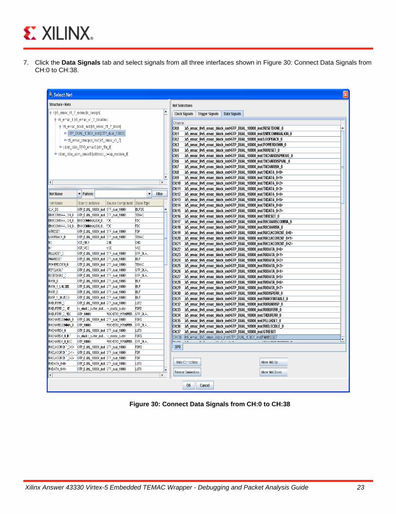
7. Click the Data Signals tab and select signals from all three interfaces shown in Figure 30: Connect Data Signals from
CH:0 to CH:38.
Figure 30: Connect Data Signals from CH:0 to CH:38
Xilinx Answer 43330 Virtex-5 Embedded TEMAC Wrapper - Debugging and Packet Analysis Guide 24
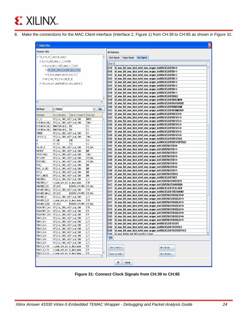
8. Make the connections for the MAC Client interface (Interface 2, Figure 1) from CH:39 to CH:85 as shown in Figure 31.
Figure 31: Connect Clock Signals from CH:39 to CH:85
Xilinx Answer 43330 Virtex-5 Embedded TEMAC Wrapper - Debugging and Packet Analysis Guide 25
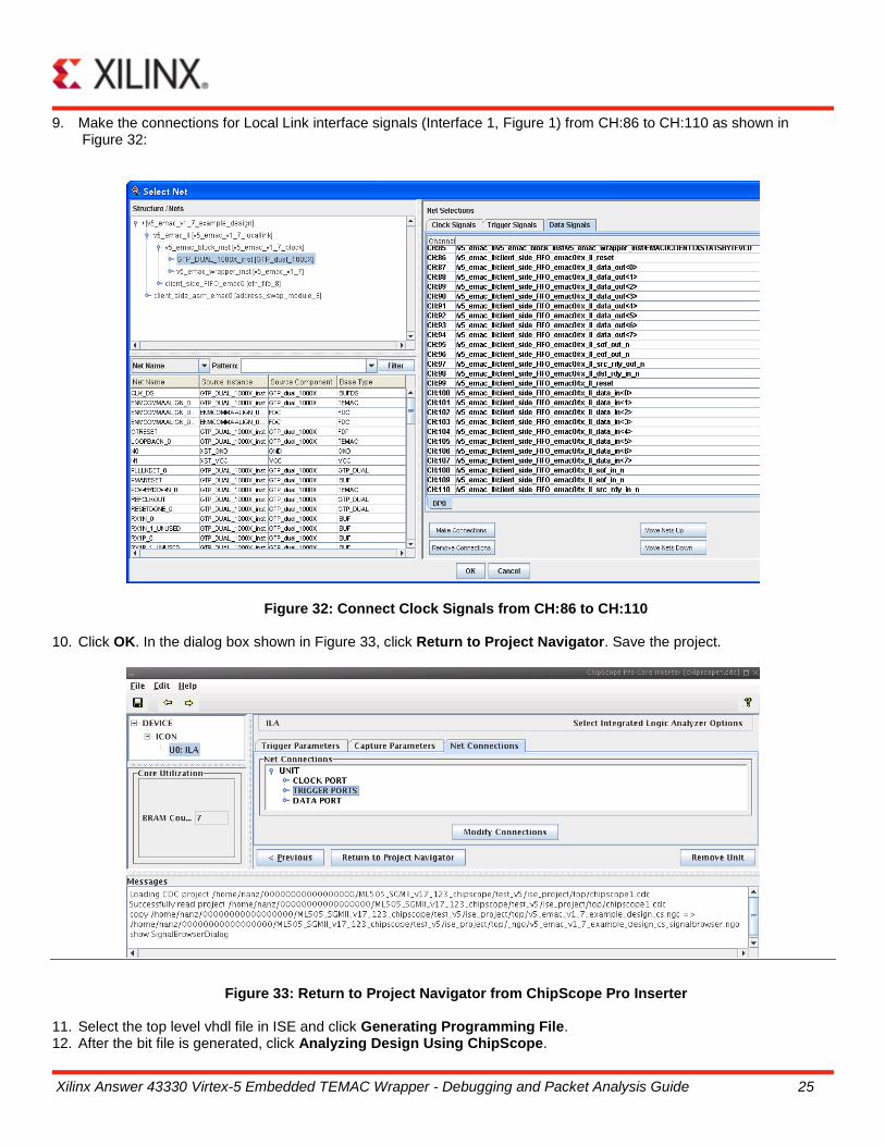
9. Make the connections for Local Link interface signals (Interface 1, Figure 1) from CH:86 to CH:110 as shown in Figure 32:
Figure 32: Connect Clock Signals from CH:86 to CH:110 10. Click OK. In the dialog box shown in Figure 33, click Return to Project Navigator. Save the project.
Figure 33: Return to Project Navigator from ChipScope Pro Inserter 11. Select the top level vhdl file in ISE and click Generating Programming File. 12. After the bit file is generated, click Analyzing Design Using ChipScope.
Xilinx Answer 43330 Virtex-5 Embedded TEMAC Wrapper - Debugging and Packet Analysis Guide 26
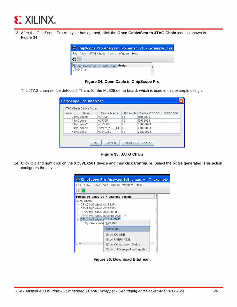
13. After the ChipScope Pro Analyzer has opened, click the Open Cable/Search JTAG Chain icon as shown in Figure 34:
Figure 34: Open Cable in ChipScope Pro
The JTAG chain will be detected. This is for the ML505 demo board, which is used in this example design.
Figure 35: JATG Chain 14. Click OK and right click on the XC5VLX50T device and then click Configure. Select the bit file generated. This action
configures the device.
Figure 36: Download Bitstream
Xilinx Answer 43330 Virtex-5 Embedded TEMAC Wrapper - Debugging and Packet Analysis Guide 27
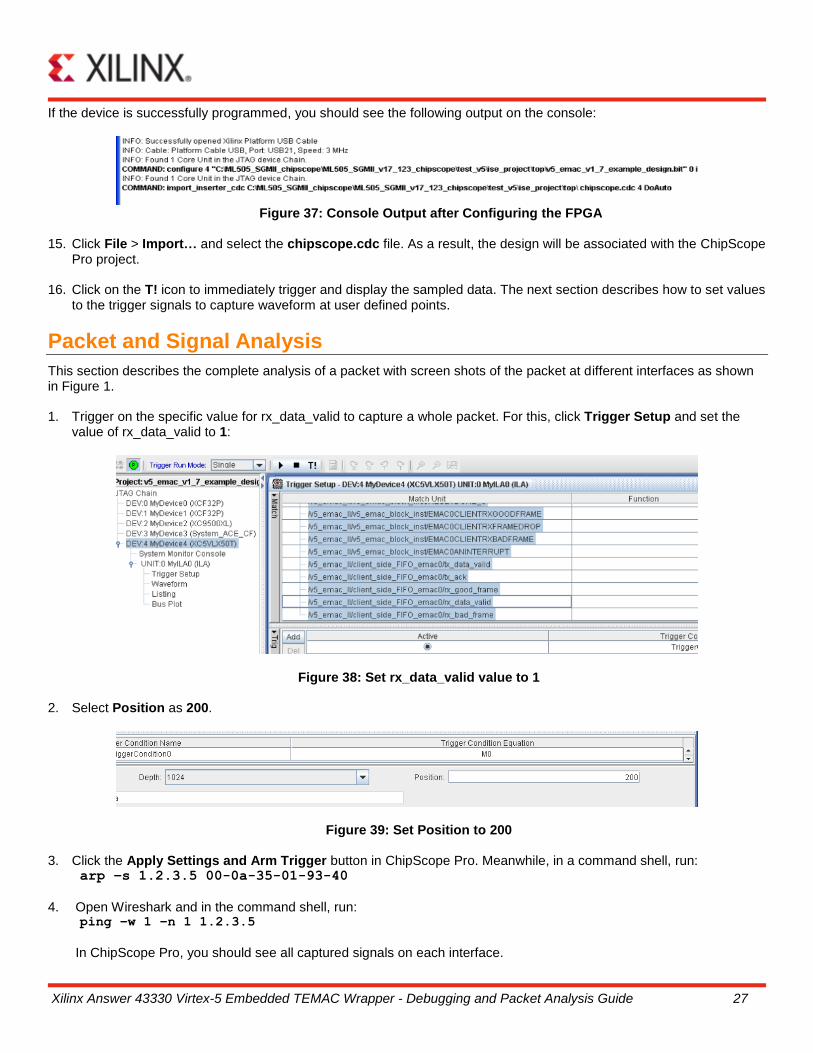
If the device is successfully programmed, you should see the following output on the console:
Figure 37: Console Output after Configuring the FPGA
15. Click File > Import… and select the chipscope.cdc file. As a result, the design will be associated with the ChipScope
Pro project. 16. Click on the T! icon to immediately trigger and display the sampled data. The next section describes how to set values
to the trigger signals to capture waveform at user defined points.
Packet and Signal Analysis
This section describes the complete analysis of a packet with screen shots of the packet at different interfaces as shown in Figure 1. 1. Trigger on the specific value for rx_data_valid to capture a whole packet. For this, click Trigger Setup and set the
value of rx_data_valid to 1:
Figure 38: Set rx_data_valid value to 1 2. Select Position as 200.
Figure 39: Set Position to 200 3. Click the Apply Settings and Arm Trigger button in ChipScope Pro. Meanwhile, in a command shell, run:
arp –s 1.2.3.5 00-0a-35-01-93-40
4. Open Wireshark and in the command shell, run:
ping –w 1 –n 1 1.2.3.5
In ChipScope Pro, you should see all captured signals on each interface.
Xilinx Answer 43330 Virtex-5 Embedded TEMAC Wrapper - Debugging and Packet Analysis Guide 28
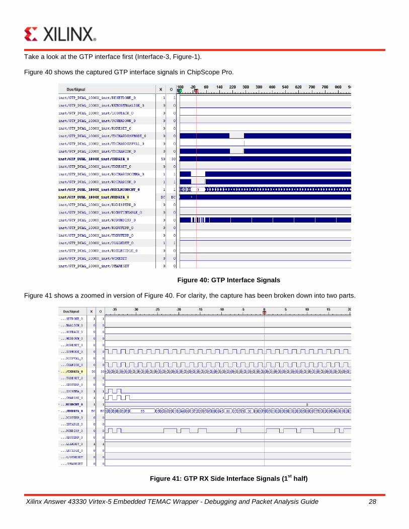
Take a look at the GTP interface first (Interface-3, Figure-1). Figure 40 shows the captured GTP interface signals in ChipScope Pro.
Figure 40: GTP Interface Signals Figure 41 shows a zoomed in version of Figure 40. For clarity, the capture has been broken down into two parts.
Figure 41: GTP RX Side Interface Signals (1st
half)

Xilinx Answer 43330 Virtex-5 Embedded TEMAC Wrapper - Debugging and Packet Analysis Guide 29
Figure 42: GTP RX Side Interface Signals (2nd
half) In Figure 41, in RXDATA, “FB” is the start of frame; „FD‟, in Figure 42, indicates termination of the frame. There are few 55s in the first column of RXDATA. This is the preamble. D5 is the start of the frame data, seen at the end of the preamble. After D5, there is the Destination Address (00-0a-35-01-93-40) followed by the Source Address (00-13-72-21-97-6f) and the data type 0800. The RX side contains data packet sent from the PC to the ML505 demo board.

Xilinx Answer 43330 Virtex-5 Embedded TEMAC Wrapper - Debugging and Packet Analysis Guide 30
Now, check if the correct data was received by examining the data frame in Wireshark. Figure 43 [a] is the Frame 1, from the PC to the ML505 demo board, in Wireshark.
Figure 43: Wireshark Data Capture (From PC to ML505) [a] In Wireshark, you can see the Destination Address as 00-0a-35-01-93-40; and Source Address as 00-13-72-21-97-6f; which are the same as you observed in ChipScope Pro. If you take a further look in Wireshark, the data from 45 to 05 highlighted in Figure 44 [b] shows the IP data.
Figure 44: Wireshark Data Capture (From PC to ML505) [b]

Xilinx Answer 43330 Virtex-5 Embedded TEMAC Wrapper - Debugging and Packet Analysis Guide 31
And the data from 08 to 69 (highlighted in Figure 45) is the ICMP data.
Figure 45: Wireshark Data Capture (From PC to ML505) [c]
This shows that the data received at the RX GTP interface is exactly the same as shown in Wireshark. The same analysis can be done at the TX side of GTP interface as well. Figure 46 and Figure 47 show the TX side GTP interface.
Figure 46: GTP TX Side Interface Signals (1st
half)
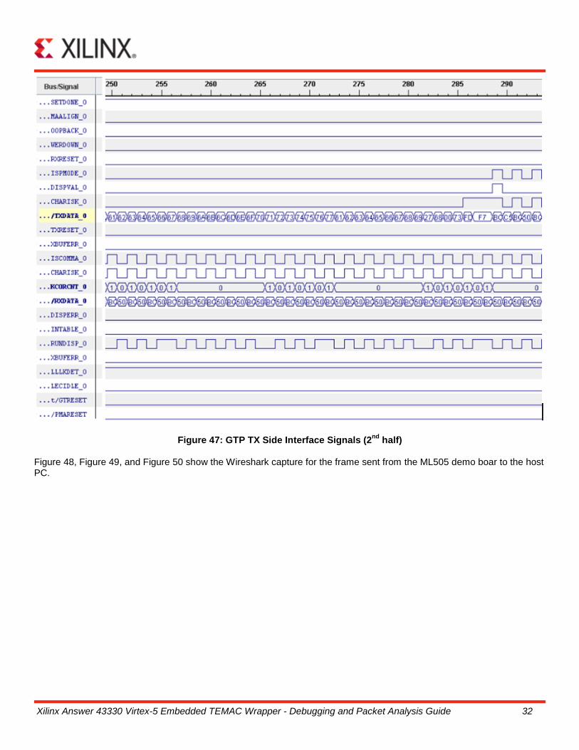
Xilinx Answer 43330 Virtex-5 Embedded TEMAC Wrapper - Debugging and Packet Analysis Guide 32
Figure 47: GTP TX Side Interface Signals (2nd
half) Figure 48, Figure 49, and Figure 50 show the Wireshark capture for the frame sent from the ML505 demo boar to the host PC.

Xilinx Answer 43330 Virtex-5 Embedded TEMAC Wrapper - Debugging and Packet Analysis Guide 33
Figure 48: Wireshark Data Capture (From ML505 to PC) [a] Here, the Destination Address and the Source Address are swapped in compare to the Frame that was sent from the PC to the ML505 demo board as shown in Figure 43.
Figure 49: Wireshark Data Capture (From ML505 to PC) [b]

Xilinx Answer 43330 Virtex-5 Embedded TEMAC Wrapper - Debugging and Packet Analysis Guide 34
Figure 50: Wireshark Data Capture (From ML505 to PC) [c] Examine the MAC Client interface signals (Interface-2, Figure 1) of all the MAC-Client interface signals in ChipScope Pro. Figure 51 shows the MAC Client Interface Signals.
Figure 51: MAC-Client Interface Signals

Xilinx Answer 43330 Virtex-5 Embedded TEMAC Wrapper - Debugging and Packet Analysis Guide 35
Figure 52 to Figure 55 shows zoomed in views of RX side and TX client interface signals.
Figure 52: MAC-Client RX Side Interface Signals (1
st half)
Figure 53: MAC-Client RX Side Interface Signals (2
nd half)
Figure 54: MAC-Client TX Side Interface Signals (1
st half)
Figure 55: MAC-Client TX Side Interface Signals (2
nd half)
In Figure 53, we can see the GOODFRAME signal goes high after successfully receiving one data frame.
Xilinx Answer 43330 Virtex-5 Embedded TEMAC Wrapper - Debugging and Packet Analysis Guide 36
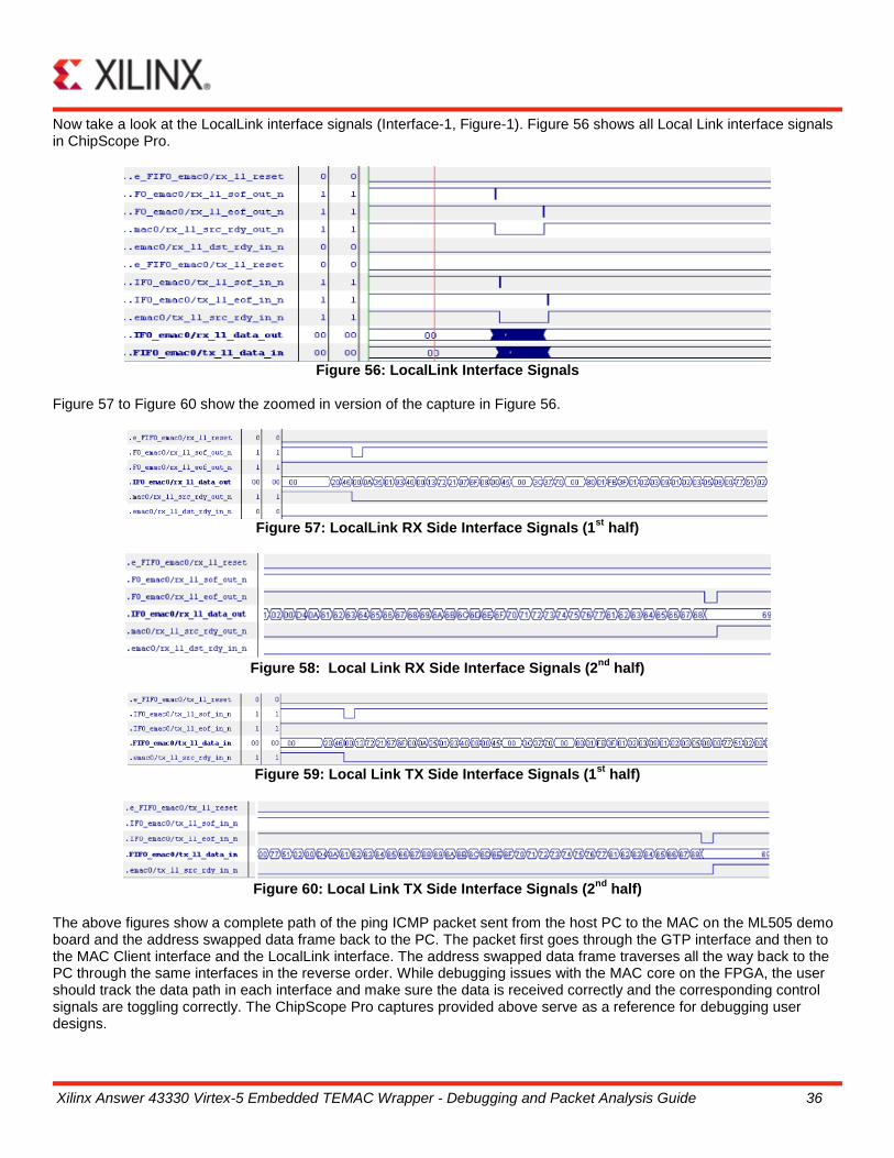
Now take a look at the LocalLink interface signals (Interface-1, Figure-1). Figure 56 shows all Local Link interface signals in ChipScope Pro.
Figure 56: LocalLink Interface Signals
Figure 57 to Figure 60 show the zoomed in version of the capture in Figure 56.
Figure 57: LocalLink RX Side Interface Signals (1
st half)
Figure 58: Local Link RX Side Interface Signals (2
nd half)
Figure 59: Local Link TX Side Interface Signals (1
st half)
Figure 60: Local Link TX Side Interface Signals (2
nd half)
The above figures show a complete path of the ping ICMP packet sent from the host PC to the MAC on the ML505 demo board and the address swapped data frame back to the PC. The packet first goes through the GTP interface and then to the MAC Client interface and the LocalLink interface. The address swapped data frame traverses all the way back to the PC through the same interfaces in the reverse order. While debugging issues with the MAC core on the FPGA, the user should track the data path in each interface and make sure the data is received correctly and the corresponding control signals are toggling correctly. The ChipScope Pro captures provided above serve as a reference for debugging user designs.

Xilinx Answer 43330 Virtex-5 Embedded TEMAC Wrapper - Debugging and Packet Analysis Guide 37
Debugging Guidelines
This document described how to use ChipScope Pro and to perform packet analysis to help debug issues in bringing up TEMAC designs. You might run into different problems during implementation, problems with transmitting and receiving frames, link bring-up, and so on. In such a scenario, consult the Debugging Designs section in the Virtex-5 FPGA Embedded Tri-Mode Ethernet MAC Wrapper v1.7 Getting Started Guide. The Debugging Designs section talks about debugging common issues during simulation, implementation, and hardware bring up. The user guide section provides a list of signals to probe during specific cases. You can use those signals as trigger signals in ChipScope Pro. For a valid
link up, EMAC#PHYSYNCACQSTATUS should be high to indicate that the SYNC_ACQUIRED state from the IEEE Std 802.3-
2005, clause 36 state machine has been achieved. Pull EMAC#PHYSYNCACQSTATUS as a trigger signal and set the
triggering point when this signal is asserted. Similarly, you can use mgt_tx_reset and mgt_rx_reset as trigger
signals to make sure that the serial transceiver is not being held in reset. Also, monitor the RXBUFSTATUS signal when
auto-negotiation is disabled. If this is being asserted, the elastic buffer in the receiver path of the serial transceiver is either under flowing or overflowing. This indicates a clock correction problem caused by differences between the transmitting and receiving ends. You can use various other signals to trigger in ChipScope Pro. All these signals are listed in Example Design Interfaces
section of this document. Some signals that you could use if you are running into link issues are PLLLKDET, RESETDONE,
RXDIPSERR, RXNOTINTABLE, and so on. PLLLKDET indicates that the VCO rate is within the acceptable tolerances of
the desired rate. RESETDONE indicates that the GTP transceiver has finished reset and is ready for use. For details on
other signals, check the Virtex-5 FPGA RocketIO GTP Transceiver User Guide. Frequent toggling of RXDISPERR and
RXNOTINTABLE indicate signal integrity issue on the board.
To check whether a packet is being received at the locallink interface, trigger on TX_LL_SOF_N for the transmitter side
and RX_LL_SOF_N for the receive side. Other signals that can be used for triggering are EMAC#CLIENTRXDVLD,
EMAC#CLIENTRXGOODFRAME,EMAC#CLIENTRXBADFRAME and EMAC#CLIENTRXFRAMEDROP. These are RX MAC Client
interface signals and indicate whether a valid MAC frame made it into the FPGA or not. After careful study of the resulting waveform in ChipScope Pro, it should provide very valuable information to debug the design. If the issue is not resolved, create a webcase with Xilinx Technical Support and make sure you describe all the details of the debugging you did and attach all the waveforms you captured. In ChipScope Pro, you could export the existing waveform into a VCD format. Before attaching the VCD file, make sure the file contains valid waveform data. A VCD file can be opened with tools such as Simvision. If you have ModelSim, convert the VCD file into a WLF file.
References
1. Virtex-5 FPGA RocketIO GTP Transceiver User Guide, UG196. http://www.xilinx.com/support/documentation/user_guides/ug196.pdf
2. Virtex-5 FPGA Embedded Tri-Mode Ethernet MAC User Guide, UG194. http://www.xilinx.com/support/documentation/user_guides/ug194.pdf
3. ChipScope Pro Software and Cores User Guide. http://www.xilinx.com/support/documentation/dt_chipscopepro_chipscope12-4_userguides.htm
4. ChipScope Pro Tutorials. http://www.xilinx.com/support/documentation/dt_chipscopepro_chipscope12-4_tutorials.htm
5. Wireshark Network Analyzer tool. http://www.wireshark.org/ 6. Virtex-5 FPGA Embedded Tri-Mode Ethernet MAC Wrapper Getting Started Guide, UG340.
http://www.xilinx.com/support/documentation/ip_documentation/v5_emac_gsg340.pdf
Revision History
08/16/2011 - Initial Release
Related Documents