VERY HIGH SPEED INTEGRATED CIRCUITS - VHSIC - N o FINAL PROGRAM REPORT N 1980- 1990 A ,-- o VHSIC PROGRAM OFFICE OFFICE OF THE UNIDER SECRETARY OF DEFENSE FOR ACQUISITION DEPUTY DIRECTOR, DEFENSE RESEARCH ANT) ENGINEERING FOR RESEARCH AND ADVANCED TECHNOLOGY SEPTEMBER 30, 1990 APPROVEI) FOR PUBLIC RELEASE: I)ISTRIBUTION IS UNINIIrrEI)

Welcome message from author
This document is posted to help you gain knowledge. Please leave a comment to let me know what you think about it! Share it to your friends and learn new things together.
Transcript

VERY HIGH SPEED INTEGRATED CIRCUITS
- VHSIC -
N
o FINAL PROGRAM REPORT
N 1980- 1990
A ,-- o
VHSIC PROGRAM OFFICE
OFFICE OF THE UNIDER SECRETARY OF DEFENSE FOR ACQUISITIONDEPUTY DIRECTOR, DEFENSE RESEARCH ANT) ENGINEERING
FOR RESEARCH AND ADVANCED TECHNOLOGY
SEPTEMBER 30, 1990
APPROVEI) FOR PUBLIC RELEASE: I)ISTRIBUTION IS UNINIIrrEI)
FOREWORI)
This report presents a description and final account of the VI ISIC program during itsten years of successfully developing advanccd integrated circuit technologies and products formilitary systems. The new technologies and the products that VHSIC has produced havesteadily found their way not only into defense systems but also into the commercial industrialbasc. They provide the reservoir from which new system capabilities are emerging and afounddtion upon which continual further advances are being made.
Over the course of the past decadtc, the VIISIC program has been active in thedevelopment of new materials, new circuit design concepts, advanced fabrication processes, newmanufacturing equipment, higher levels of radiation hardening, new data interface standardsand specifications, and improved techniques for built-in-test and maintainability. The VI ISICHlardware I)escription Language and other design autonmation tools have broken throughmajor integrated circuit complexity barriers and will decrease the cost and the development(niwc of modern electronic systems. The resulting 1:chicvemenls have he!pcd to produr' a newlevel of sysctm dcsignr and tahrication --- one that approaches an integrated conccpt-to-systemncapability, i- .7
The broad scope of Itchnology that VI ISIC activities include-d and the almost universalapplication of IC technology in in ilitary systems required an unusual structure andmanagement strategy for the program. Although most of the technology work was in the"research and developmcnt" category, the identified goals and near term objectives weie toinsert tihe technology products into systems as soon as possible --- either as updates to then-current systems or its enhancements to systems in the design and development phase. In"•1Jidtion, the applicahility of almost all of the technical achievements of the program tocommercial IC production meant a continuing high interest on the part of the entiresemiconductor industry in the progress of the program. A L-orresponding responsibility wasicquired on the part of the VI IS(IC program managers to consult with the industry leaders andhe aware of I heir concerns. Finally, since the technology was (and is) broadly applicable totlhe electronic system requirements of all tile Military Services, a1 intCgrated l)DCpatrtmclt ofI)efense management was adopted which involved the participation of technical and contractmanagers at the Services" hcadquautcrs and techical specialists from many of the Servicelaboratorics.
The results of the VI ISI(C programl will continue to he absor-hed into induttlrial practicea rd l)o I) procurLmCnl for many years as new IW production capabilities aire achieved and newsvstems designs are placed into operation. Continuing developmie nts in ilteCgratcd s'stclildesign techniqucts will allow a design, simutmht ion, and re-design i)Jocess t hat CeStLire-s oIpt i tintpe 1rformance at low developmnenii t cost.s. The cýoltutiol of the (.)tulificd N Manufacturing ! :neproceditre will matkc it p ssihlc to producc highly complex ICS as nimilitary qualified inrtsWithout incutirring cxcc.ssi vc qualificatilo costs.
iii

PAGESARE
MISSINGIN
ORIGINALDOCUMENT
The legacy of the VIISIC program is a broad spectrum of technological advances, tileenhanced military capabilities, and the maintenance of U.S. leadership in an area of technologythat is vital to our national wJll being.
In carrying out its activities the VI ISIC program involved a major portion of the U.S.semiconductor industry and a considerable number of technical managers and specialists in theI)epartment of Defense. The success and achievements of the program would not have beenpossible without their leadership initiatives and dedicated, enthusiastic efforts.
~~. MdLc( JilumDirector, VIISIC Program OfficeO)DI) R /R&AI"
iv
CONTENTS
CHAPTER I - EXECUTIVE SUMMARY
Background and Program Objectives ... ................................. 2Program Structure ............................................... 3S ecu rity . . . . . . . . . . . . . . . . . . . . . . . . . . . . . . . . . . . . . . . . . . . . . . . . . . . . . 7Program R esults ................................................ 7
Design and Design Automation ...... ................................ 9Fabrication and Manufacturing Technology .. ......................... 10System Insertion ...... ........................................ 12Technology T ransfer ........................................... 13
The Impact of VIISIC - Leonard R. Weisberg ............................... 14
CHAPTER 2 - THE VHSIC IPROGIRAM HISTORY, STRUCTURF, AND POLICIES
2.1 Program Origins and Objectives .................................. 24The Legacy of VIISIC - Larry W. Sumne. ............................ 26
2.2 Program Structure ............................................. 302.2.1 Phase 0 Concept Definition .. ............................... 302.2.2 P hase I . .. . .. . . . .. . ... . . . . .. . . . . . . . . . . . . . . . . . . . . . . . . . 3.322.2.3 Phase 1 Yield Enhancement ... ............................... 342.2.4 Phase 1 Technology Insertion .............................. 352.2.5 Phase 2 Submicrometer Technology Development ................. 352.2.6 Phase 3 and Other Supporting Technologies ...................... 372.2.7 D esign A utom ation ...................................... 382.2.8 VIISIC Manufacturing Technology Program - .Joscph A. Key ........ 39
2.3 Program Management ....... ................................. . 402.4 F unding . . . . .. . .. . . .. . . . . . .. . . . . . . . . . . . . . . . . . . . . . . . . . . . .. . .. 422.5 Security - James J. I lower .......................................... 42
2.5.1 H listory of VIISIC Security Measures ... ......................... 422.5.2 Additional Security Decisions ... .............................. 47
CtAPI"TER 3 - DEVELIOPMENT TASKS
3 .1 D esig n . . . . . . . . . . . . . . . . . . . . . . . . . . . . . . . . . . . . . . . . . . . . . . . . . . . . 50The Impact of VIISIC on System Level l)csign - Robert W. Rolfc........... 51
3.2 Test and Life Cycle Support .................................... "743.3 C hip Fabrication ........................................ .... 88
The Impact of VHSIC on FMbrication Technology - Charles S. Meyer ....... 883.4 Description ot VH SIC Chips .................... ............... 120
v
('14APTIER 4 - IRASSBOAIR) I)EMONSIRATIONS
4 .1 P h ase I .1 . . . . . . . . . . . . . . . . . . . . . . . . . . . . . . . . . . . . . . . . . . . . . . . 14 24.2 P h ý, . 2 . . . . . . . . . . . . . . . . . . . . . . . . . . . . . . . . . . . . . . . . . . . . . . . . . . . . 14 5
CHAPTER 5 - 1TICIINOLO(;Y INSERTION
'l[he Impact of VIISIC on the 1)ol) System Life Cycle - Joel Nv. Schoen ....... 150.1 Army System Insertion Projects .................................. 154
5.2 Navy System Insertion Projects ................................... 1605.3 Air Force System Insertion Projects ..... ........................... 1645.4 Other System Insertion Projects (Namic only) ........................... 1705.5 Logistics Retrofit Engierirg ......................................... 1725.6 Projects Involving VI II)L Insertion .................................. 173The Impact of VIISIC on D)oI) Weapon Systemis: A Case Study
- John E . S tuelpnagcl ........................................... 177
CHATEI'R 6 - TI'ICNNOLO(;Y TRANSIER
6.1 T rain ing . . . . . . . . . . . . . . . . . . . . . . . . . . . . . . . . . . . . . . . . . . . . . . . . . . . I ,);6.2 Conferences and W orkshops ..................................... 1866.3 Technology Transfer of Design Tools ................................ 1906.4 Testability and Built-In-Self-Test .. ................................. 1916.5 Commercial Applications .......... ............................. . 192
CHlAPTER 7 - VIISIC INDUSTRIAL BASE
The Impact of VIISIC at IBM: A Case Study- Robert II. Estrada and lHarley A. Cloud . .......................... 197
7.1 I)esign and Manufacturing Capabilities .............................. 2007.2 Commercially Availahle VI ISIC Design Tools ......................... 213'ihe Impact of VIIDL on Design Autonmation - Randolph F,. I larr ........... 213
ACKNOW LEID GI,'ILNTS ........................................... 229
APPENDICES
Appendix A - References ........................................... 231Appendix B - VHSIC Contracts .................................... 243Appendix C - Glossary . ........................................... 259
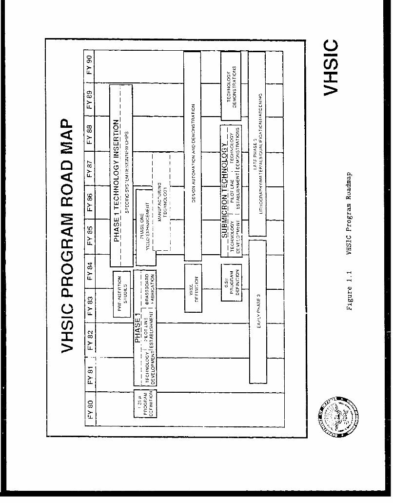
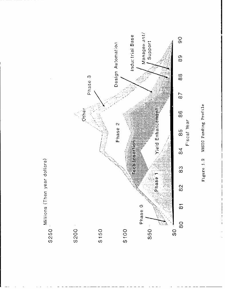
Figures:1.1 VHSIC Program Roadmap .. ................................... 51.2 VHSIC Funding Profile .......... ........... ... ....... 62.1 VHSIC Program Roadmap .. ................................. 433.1 Built-In Self-Test Features (TRW ) .. ............................. 593.2 Relationship of Frameworks To Application Domains .............. 723.3 SOS-Ill VHSIC Phase 1 Process (Hughes) ....................... 923.4 PPP Architecture Partitioning Into Chips (Honeywell) .............. 1233.5 Single Channel Digital Correlator (Hughes) ...................... 1253.6 Complex Multiplier/Accumulator (IBM) . ......................... 1273.7 Data Processor Unit (Texas Instruments) ........................ 1283.8 Window Addressable Memory (TRW) .......................... 1313.9 Pipeline Arithmetic Unit (Westinghouse) ........................ 1333.1(i Array Processor Unit (Honeywell) ............................. 1353.11 Systolic Processor (IBM) . .................................... 1363.12 Central Processing Unit, Arithmetic Extended (TRW) .............. 1395.1 Programmable Signal Processor Improvement ...................... 1785.2 Advanced PSP Architecture .................................... 1805.3 Airborne Surveillance Radar Processor ........................... 181
Tables:1.2 VHSIC Chips Demonstrated in Phase 1 and Phase 2 . .............. 81.1 Major Events, Milestones, and Highlights ..... ................... 202.1 V HSIC Funding H istory . .................................... 443.1 113M 0.5 Micron CMOS Technology Features ..................... 1023.2 VHISIC Phase 1 Chip Characteristics ........................... 1213.3 VIISIC Phase 2 Chip Characteristics ........................... 122---------------------------------------..............
SI I
ci.. ...0
A l
v ii " .. .
CHAPTER I - EXECUTIVE SUMMARY
Background And Program Obi ectives .................................
Program Structure . ................................................. .7
S ecu rity . . . . . . . . . . . . . . . . . . . . . . . . . . . . . . . . . . . . . . . . . . . . . . . . . . . . . . . . . . 7
Design and Design Automation .................................... 9Fabrication and Manufacturing Technology ........................... 10System Insertion ..I ... .. ..... .. ... ..... .. ... ... .. .. . .. . .. . .. . . . 12Technology T ransfer ........................................... 13
The Impact of VHSIC - L.eonard R. WXcisherg ............................. 14
CH1APTEIR I
EXEICUTJ[IXE SUNINIAWR
III March 19,80, thle Department of lDefense began the V'ery High Speed IntegratedCircuits (VI ISIC) programi to deveIlop advanced silicon integrated circuits. In September1990, thle VI ISIC programl oftiCiall\' came to anl end in termis of starting new activities. Duringthle intervening decade, wNithl funding of approximately $918N4, VIISIC organized thle effortsof hundreds of engineers, scientists, and managers, and scores of companies in a highlytechnical and complex enterprise. For much of that time VHSIC was considered one of thlelioghest priority technology program tin thle lol) and of vital imotac to sustainling thlemilitary superiority of the United States. TLhis Final Report is an update to and summary ofthe Annual Reports for 1986, 1987, and 1988 (References 2.27-2.29). Together, these fourreports providIe an overall dlocumentat ion of the VI IS IC program.
This report presents the rationale and objectives of thle program, the organization andstructure through which it directed its efforts, thle results that were achieved from its manYvactivities, and indepenldent ass"essments ot thle impact that it has had on Integrated circuittechniology and Its ulse InI military' systemls. Such an assessmtie nt byon of the primary initiatorsof the \VI ISIC Program is included at the end of this Executive Summary.
VlISIC i.% ou). highest /)riOrit , ' lec hilOIW,' (uld we ~itill coliillue to pr)-i~dt'
t,Wohr4 m)ahUgllaIp t lcl emphasis ill ordeFr to (U hieci' the i/urease(I mIliitdF capa)(bility
L'XI)L't('d /)1omn its resiuIh x.'
-Ricluard J). [)ehaitr. Undicer Sec reta/vy of 1w.1f'Clim, Thr Research andAl,z1'uilc'jou,'. Stcitc',ncu to die Ylzh ('aI C 'n'rss- First Session, A'Iarch 1983.
Background And Program OlbJectives - (Chapter 2)
P~rior to 198(O, the IDoI) had spent several years carecfully assessing its needs anddeficiencies inl Integrated circuit technology The major deficiency perceived was that theD~OD I) dpoymenCIt of' military products Incorporating state of thie art microelectronic technologywas runnling tenl or more year's behlind the appearance of that technology in thle commercialmarket. WVorse still, the delay was increcasing with timec. I lowever, the need for ready accessto this technology had becomle increasingly vital to thie U.S. defense posture as thle weaponsystems being deployed bCcamei m1-ore and mote depci ident Onl electronic subIsystems for- theireffectiveness, for 1I hci speed of' response, and for thecir adlaptabi Iity in rapidly changing battleeniviron ienclts.
CHlAPTEi I / I XECt IFIVE SUMMARY
The goal of the VIISIC programn was to correct that deficiency by giving systemdevelopers and acquisition managers a military qualified mIicroelcctronics technology that wason par with or better than the technology available commeurcially.
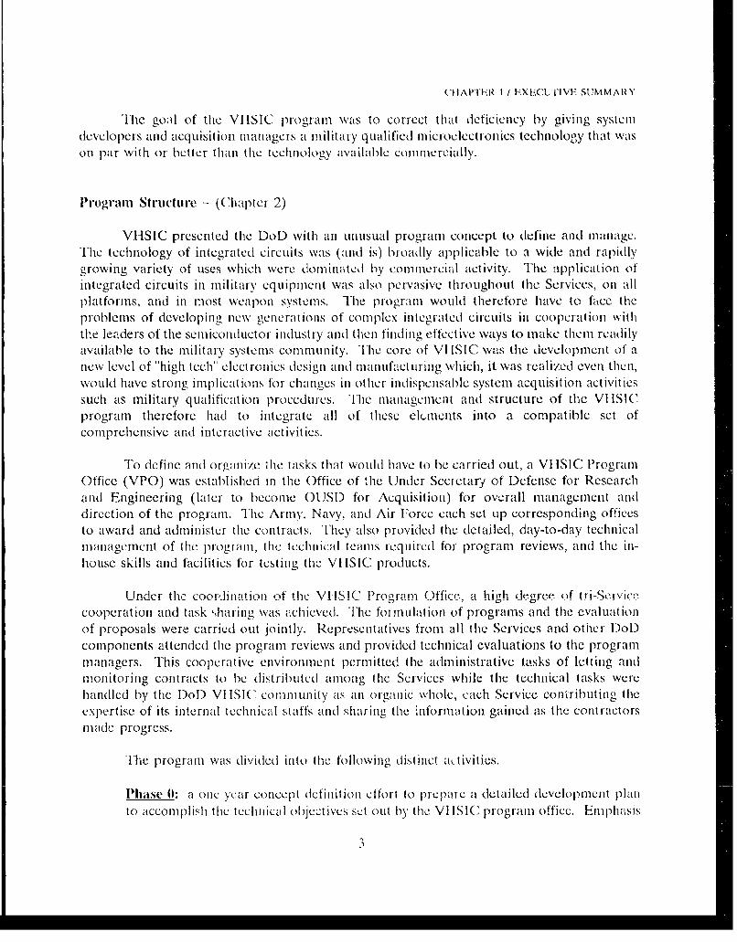
lPrograIml Structure - (Chapter 2)
VIISIC presented the DoD with an unusual program concept to define and manage.The technology of integrated circuits was (and is) broadly applicable to a wide and rapidlygrowing variety of uses which were dominated by commercial activity. The application ofintegrated circuits in military equipment was also pervasive throughout the Services, oil all
platforms, and in most weapon systems. I-lie progpran would therefore have to face theproblems of developing new gCnCratiolls of complex integrated circuits in cooperation withthe leaders of the semiconductor industry and then finding effective ways to make them readilyavailable to tile military systems community. The core of VI ISIC was the development of a
new level of "ligh tech" electronics design and manu.1facturing which, it was realized even then,would have strong implications for changes in other indispensable system acquisition activitiessuch as military qualification procedures. Tihe management and structure of the VIISICprogram therefore had to integrate all of these e lments into a compatible set of
comprehensive and interactive activities.
To define and organize the tasks that would have to he carried out, a VItSIC ProgramOffice (VPO) was establishied in the Office of the Under Secretary of Defense for Researchand Engineering (later to become OUSD for Acquisition) for overall management anddirection of the program. The Army, Navy, and Air Force each set uIp corresponding officesto award and administer the contracts. They also provided the detailed, day-to-day technicalmanagement of the program, the technical teams required for program reviews, and the in-house skills and facilities for testing tile VI ISIC products.
Under the coordination of the VIISIC Program Office, a high degree of tri-ServiCecooperation and task ';haring was achieved. The foximulation of programs and the evaluationof proposals were carried out jointly. Representatives from all the Services and other Dol)components attended the program reviews and provided technical evaluations to the programmanagers. This cooperative environment permitted the administrative tasks of letting andmonitoring contracts to he distributed among the Scrvices while the technical tasks wverehandlcd by the Do!) VI ISIIC community as an organic whole, each Service coniribut ing theCxpertise of its internal technical staffs and sharing the information gained as the contractorsmade progress.
The program was divided into the following distinct ac tivities.
IPhiase 0: a one year concept definilion effort to prepare a detailed dcvclopmcnt plan
to accomplish the technical objectives set out by the VIISI(C program office. Emphasis

CIHAPTER I / EXECUTIVI- SUMMAIRY
was put on 1.25 micron minimum feature size and 25 megahertz clock speed. Ninecompanies participated in I Lla " 0, starting in March 1980.
Phase I: a primary effort, based on the approaches defined in Phase 0, to develop andproduce silicon chips with 1.25 micron minimum feature sizes and 25 Ml 1z clock speed,and to demonstrate them in subsystem brassboards. Phase 1 contracts were awardedto Honeywell, I lughcs. IBM, Texas Instruments, TRW, and Westinghouse in May 1981.
This phase was later expanded to include a yield enhancement program to increase theyield or producibility of the VI ISIC chips.
Nanlufacturing Techniology1: the duvelopment of better manufacturing tools andtechniques that werCe nccded to make lthe VIISIC chips prodiucible and affordable.These projects were defined and funded jointly with tile manufacturing technologyprograms in the Services.
Design Automation: the development of the design tools, standards, software, andhardware needed to make the design of large, complex VHSIC chips more effectiveand affordable.
"lechnoloav Insertion: the demonstration of VIISIC Phase ! chips and technology byinserting themi into a broad variety of military systems, both existing systems and othersstill in development. In cooperation with the system program offices, VI ISIC co-fundedboth feasibility studies and demonstrations of hardware in operating systems.
Phase 2: a primary effort to develop and produce (on a pilot line basis) silicon chipswith 0.5 micron minimum feature size and 100 megahertz clock speed. This phasewas started after it became clear that development of the 1.25 micron technology andits transition into manufacturale1c products could, in fact, be accomplished. Thecontractors selectted to ilnuirfa keo the iihnllicron (deve.l~lome_.nt tasks were I loneywel!,
IBM, and TRW. Contracts were awarded and work began in November 1984.
Phase 3: a broadly based collection of separately funded contiacts conductedconcurrently with Phases 1 and 2. These supporting technologies were found necessaryto meet the prcgram objcctivcs. Specific efforts were undertaken to deal with teclino-logy applications, materials requirements, lithography and fabrication tools, designsoftware development, packaging, chip qualification, and radiation hardness.
A ", oadmap" of thliese program activities and the overall program funding profile from19,() to 199(0 are shown in Figures 1.1 and 1.2.
4
00
LLL
00
w -
U- QI 0
IF I <
LL0
_j I rZ z-i~ r
00 r 0
D I 1 2'r
LL <0 IV
CO I ZI
I~ u-i~ 0 0O j
00
LL0cr 9 2 . C: t
0'cc V-
0LL L
CLLi_ _ __._ _
Q)
4- .4-
cl00
CYC
"..........
L0i
co
...................
A/Y//"~'/$ O
-00 cz~4U.1 QJ
0 :.74;44/7/;.4;.00
w 0
CC)
co
0~~ LO\ 0 C
(I \flRI /I FXF CH I' \IV' SUMNMAR V
*IeIC l1ouse anld Scutite (Thdlncicet IRepori for (thc 19s(1 IDcfenlse budgeýt, whichautho; 11Iie thle in it iii 11,undi ig 1ot 111 VI ISI I (ipI11111ila, Included thle following statciement:
"I/flc (t /i( b ( I(( 11 (40. I/i dt' V i/ope .1i' 1116 U I/ ( Vi IINIC.) flroi'Fd/ would be
lchl ol 1i;ý pi'oyn..ý.w.N lo //uI(. 'i/il h/2 Ith l O! 110 11 nid W un ' ,Ilri.s ity fa
Thits stateme nt ucipresenited Z, dc i'l:um t ire t 11n he existin adminilstrAtive Controls oilin iCIOC led ronlics. ()nl t hti. i-~ i s sped I wall designed for mnilita ry applicat ion hadp1 eviouslv beenl k: -,a llcd h\ "11C I ARN. All1 duail -1se of gC1cn at pulpst devices, eVell t hosemul 1() to i1 lit af r \ pecifi callo bt\, X\CI ecci intl cdit nde I (thc I xport Adm mistiation PRegulationlS(FAR) of t he I )cpa U micl kit of (\a nmccc.
A"s t11e DI')emn VI 1SR( Pio~tailn otticrali camel lo an1 enid, ihe VI() nlo longerlC0onSiltcId it nicce~ssa; oI aIpplopt iatc to sinwlc o: t VI 151(7' dev ices for special control. Thetlet 111 of I e(ti 'on lpcssii illaI mandmi c fin jclcie ti om I I AR control were meit by the diffusionlof (he techniologN t hrou l~ou~t ne~ Ii odust IY anid thle subseq uent availability of comparabletechnologiiy InI Fluopc anti the v\k"clci PaIcific.
'I lhe \ P( ak 1st suppor t.d a t lI 0ioi .IIL 111 t hic us o! dciclc!s lICveIopecl under. U)is ProgramI)cnil I ClllcciO ZI)applica I joltS. SLItCh11 dtcViCC, \Wltt hi be pOpe lv1 iden~tified ZI 'dualZI-uIse and wouldhien he subject to thev sa met I ARN ~ontlo 'I"i s0 ohic colin mci cial integratctl circuit deVices.
Pi-ogirami Re'sult s
il 0CICe rcIudtI Of IheI decatic f 111.or iv. Aodce 1wthhVloI pora ae unatipintercnainc f ii \'U ~ Smmtv Acgoooy of some of thle mlore siginificant
eventsl that occur ici durli me th couisc of thLc priol,,jtmi are listed inl Table 1.1 at thie etild of thischap1-tter. more del a iI alre (Iescr bed H, r' inplceis 2 thirough 7 of this report. Thc mostComplete technical account ',Illa the t10 VA di ci i11ntent loll of results will he found inl therefcienccs t hat aie listed in Appic ldix AN. I icl udcd Iat appi opriate places throughout thisreport are Individual as,,sessiiwli of thev VI 1151 piogi ami which have beeni conitributed bypeople who hlave eCt~il imist I outsidokc ') ilt- h VII SI( 'program oft ilce-s but who have participatedinl Vi ISI(, activlIt. l Nc iii vat I jo 10"s pisloni. Iah m it1 blilltionl provides anl evaluation, froml thleaut hot's peý-solnmlp' r~ c oft 11ek 111-1,1 t11t VI I[SIt' has, had either ol a conipanly position
wit repclto Wi) techn~lolopy. on id) a ) I ) alica Ions1 of W( tcchtology, or oil particular areasof IW ehn.iig
-7
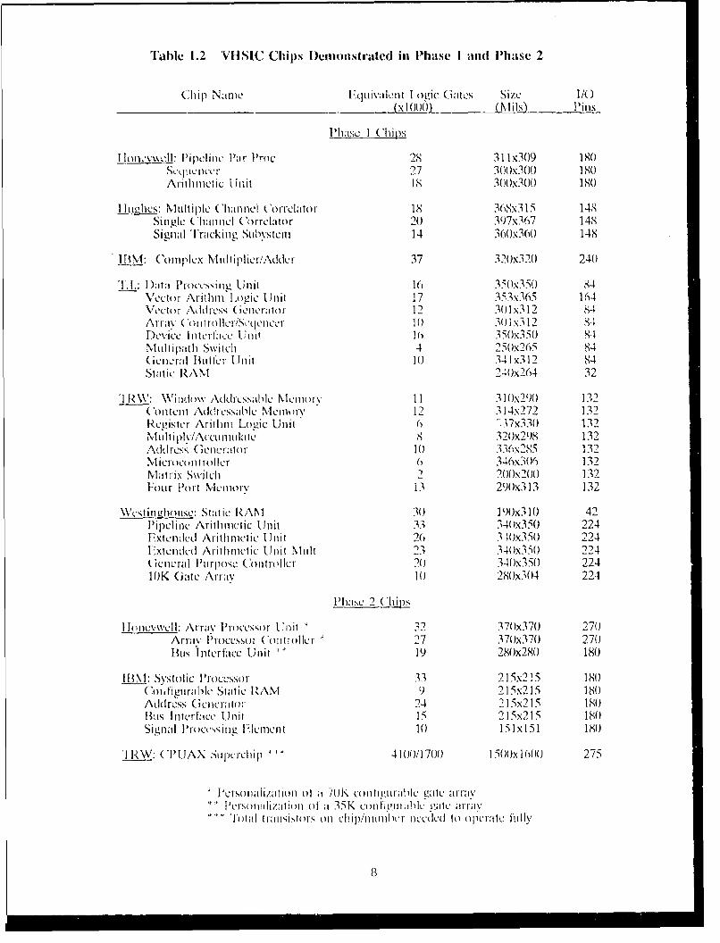
TIable 1.2 'V[IISC CldPs D~emonostrated in Phase I and PhIase 2
(hip Nanic biov Len ogic G.'I;Ics SizC /(x 1000) (NIils) pins
lliase I ('hip~s
I onvd :Pipelno: Pa~r IProc 28 31 10x09 1 WS"qllcilccr 27 3000300 180iArithnictic Unit 1s 300x0() 180
I Iitglics: Multiple C hainnel 1. orreclator is 368x315 148Sin~gle Cihannel ('orreclator 20 3970367 148Signal TIracking Stihvstem 14 360000( 148
ITI~NA: Conmplex N'Iiltiplier./AdderI 37 320'x320) 240
A. I.: Daita Proccs'i ni Uniti I1(1 3500350 84Vector Arithim Logic Unit 17 3530365 104X'eetnr ,Vhlrcss ( iclirator 12 30] 0312 84Arrav ('0111llrS~ee 10 3010312 84fDev\ice Intertface Unilt 10 350035( S4Multipalth Switch 4 2-50x2605 84(jeneral:1 BtIifCr Unit 10 3410312 84Static. RA\Id '240Ž264 32
'I k \\: Winidow Addrcssalhlc Menu ory 11 3] 0x'-90 13',2Conitcnit AddreCss.hle Nk ilntt 12 3 14x272 132Registcr Arithim Logic Unit 0 ',37x330) 132MLNIII ply/Accumidailae 8 320)x2958 132Address ;flrý tr1 336N285 132NMicroco i i )I c r 6 340x'3(t6 132Mat rix Switch 2 1200x20t)0 132lollr Port Meniorv 13 2900313 132
\Vcstin ~tiIuse: Static RANI 30 1 900310 42Pipe)cliuc Arithmetic Untiit 33 340035( 224Fxtended Arithlinitie Unmit 26 310,0x50 224:xtended Arit n\Ietitc U nit Miilt 23 3400%51 224
( icileral Ptirpose Oiontroller 203400350 22410K Gate Array 10 28003O4 224
]PIise 2 (Chips
1Ilonevxvell: Array 1'rncceýssr Un Jit 32 3700370 270/\rrav 1Prneessor ('oatrollcr 27 3700370 270BIS ijsltcrlacc Unit t~19 280x2S0 180
113NI: Systolic 1'r-occSsor 33 21]5x2!15 180(,Oil it'irahhT'Il Sta'tic RA\M 9 21 57x2 15 180Address (ienerato 24 21 5x2 15 180Mis Interfatce Unit 1.5 215x215 180Shia rcsii~Lcun 10 I51xi~ 180
'I KW: ('1 JAX Supcrcllip 4100/1700 1 5(OOX 1 000 27.5
i'Ctsonlalizatiou of ai /OK Ct)IIItL1IraIhIC gate arrayiPaesouuilization od a 351K eonti'iYmdIr : alecat ra
Tintal tralvtsbtors oil Ch'lui)/ItItIeINr nee..ded to opwrate fu.lly
8
CHAPTER 1 / EXECUTIVE SUMMARY
The direct activities of VIISIC were concentrated in four broad areas -..- design anddesign automation, fabrication and manufacturing technology for VHSIC chips, insertion ofVHSIC products into systems, and the transfer of the technology into the broader industrialcommunity involved in military system development.
Design and Design Automation: (Chapter 3, Sections 3.1 and 3.2)
Twenty-nine chips for Phase 1 and nine chips for Phase 2 were designed, produced, anddemonstrated during the VHSIC program. They constituted very complete and powerful chipsets which were capable of performing the wide variety of signal processing functions neededby military weapon systems and were used experimentally to explore specific systemapplications. These chips are listed in Table 1.2.
In order to design chips of such functional complexity and large physical size, theVI-SIC program needed advanced design automation tools. Design standards were alsoneeded to make sure that the resulting chips would operate successfully in real systemenvironments. The VI ISIC efforts in this very dynamic and rapidly growing field of technologyhave had a strong influence on many of the directions taken in design tool development. Themost visible influence has been the development of the VHSIC Hardware DescriptionLanguage (VHDL) which was adopted as a international commercial standard by the IEEEin December 1988.
The VHDL provides a powerful computer language by which both the hardwarestructure and the electrical behavior of any IC can be described. The VHDL description canbe used in the design process to simulate the performance of the chip and make sure that itwill operate as desired. It can also be used to generate the computer programs for testing thechip after manufacture, to transfer the design data from one company to another for secondsource production, and to provide archival documentation of the chip design in case it needsto be remanufactured in the future, As a result of its usefulness in the acquisition andmaintenance of electronic systems, VII)L has been adopted as a DoD requirement formicrocircuit documentation.
"ASIC dotinulntation in VIIIDL. Digital Appli.ation-Speci fiu Integrated Circu.its(ASICs) deLsigned after 30 September 1988 shall be doc'tiented by vineans of.structural and behavioral VIlSIC Ilardware Description Language (VHIDL)desc riptions inl cc'ordalnce with IEEE 1076. lBehavioral VI-DL descriptions shalldescribe the input/outJutl behavior at a sit ' Ilicientl) dletailed level to permit thebehaiiviral d' ril fitn i1(' 1.•u 1, ld within a lI'.ei VIIDL model for testgeneration and J1,l0t/1 grading of the c'onlaining model.
9

CHAP LIZR 11 IEXECUTIVE SUMMARY
Fault coverage. Fault coverage shall be reported for the manufacturing-level logictests for all digital inicrocircuits demi,,ed after 3(0 September 1988. Faultcoverage shall be based on the equivalence classes of single, permanent, stuck-at-zero and stuck-at-one fatdts on all lines of a TISSS-comipatible structural VIlDL
model, where the structural model is e.vpressed in terms of gate-level primitivesor simple atomic fiections (such as flip-flops)."
DOD All L-STD-454L, Requirement 64 (Microelectronic Devices)
September 20, 1988
VHSIC also emphasized the need for system level design tools. The increasingfunctional complexity of VHSIC chips was bringing the concept of an "electronic system ona chip" much closer to realization and so the design of individual chips was no longer isolatedfrom the design of the overall system. The Architectural Design and Assessment Systcmwhich was developed under a Phase 3 contract has found widespread use in the design ofoptimal system architectures. The development efforts begun by VHSIC have been continuedin many cases under separate Service sponsorship.
VHSIC required that testing capabilities be built into the chips so that they couldprovide self-generated data on their readiness to operate. This requirement resulted in thedevelopment of very sophisticated built-in test design methodologies that are now in use.
Four standards were dcveloped to provide for the interoperability of VHSIC chips witheach other and with the other system ;omponents. The standards include an electricalspecification for direct interfacing of all VIISIC chips, a parallel interface bus for messageand data communication onl a systcm backplane, a serial test and maintenance bus for sendingand receiving test data signals on the ';ystem backplane, and a serial element test andmaintc.nance bus tor test data communication with individual chips on the same circuit board.Thcse standards are part of a group of data bus and interface standards that were developedand transferred to the larger industrial (and international) electronic community for use in thecontrolled exchange of data.
Fabrication and Manuffacturing Tcchnology: t(ChaptcrL3ection 3.3
The VI 1SI" contractors developed tcchnologics for fabricating the complex, large area,signal processing chips first with 1.25 micron and then with 0.5 micron feature sizes. Theyaccomplished this on timne schedules which, in both cases, produced manufacturing prototypechips ahead of the time schedules for the production of equivalent commercial chips. Twenty
1(1
CHAPTER 1 / EXECUTIVE SUMMARY
nine different 1.25 micron chips and nine 0.5 micron chips were designed, fabricated, anddemonstrated. Many new and difficult fabrication problems had to be solved, especially in theareas of silicon substrate material, fine-line lithography, multi-layer metalization, andpackaging.
"...most experts agree that wiihout VHSIC, semiconductor development in the U.S.wi'ouldn't have progressed so quickly toward submicron geometries, even in the
commercial world ."
"Among the technical breakthrou hs spawned by VHSIC is the use of multiple
layers of wetal in advianced semiconductors, now a routine design lfeature inhigh-density ICs."
"What Did We Get From VHSIC", Electronics, June 1989, p. 97
The first VIISIC chip with 1.25 micron technology was produced in February 1983.
Since that time, the technology has evolved into a full production capability at a large numberof industrial manufacturing lines. A representative list of such companies with their VHSICmanufacturing capabilities is included in Chapter 7.
The culmination of the manufacturing technology developed in the VHSIC programwas the successful fabrication anmd operation by the Phase 2 contractors of highly complex,
capable, 100 megahertz, 0.5 micin chips. IBM demonstrated a set of four signal processingchips in an acoustic beamformer brassboard in December 1988, TRW demonstrated an
operating VHSJC "superchip" in December 1989, and 1Honeywell is scheduled to demonstrate
a set of three customized gate array chips in a cruise missile guidance application inSeptember 1990. The TRW "superchip", for example, measures 1.5 inch by 1.6 inch and
contains over 4 million transistors. More than one half of the transistors are used as
redundant elements that are automatically switched into operation, if needed, to ensure that
the chip is functioning properly before it leaves the manufacturing line. This designicharacteristic also guarantees that the chip will have an extraordinarily extended lifetime insatellite applications or other unattended operations.
After an intensive effort on manufacturing yield enhancement, the various Phase 1chip types were produced on pilot production lines at yields that ranged froim under 10%,which is marginal for production, to over 70% which is high enough to enter confidently intofull seakl pi oduetiuii
11
CHAPTER 1 / EXECUTIVE SUMMARY
One of the major requirements of VHSIC was that the chips be operable in severeradiation environments. In coordination with the Defense Nuclear Agency, the VIISICprogiam developed fabrication technologies which could, by the end of Phase 2, produce chipsthat were fully capable of meeting military radiation hard specifications at very little, if any,extra cost.
System Insertion: (Chapter 5)
A very substantial portion of the VHSIC management efforts and funding went intoapproximately twenty-seven system demonstration projects in which VHSIC chips and boardswere integrated into system hardware so that the benefits and advantages could be realisticallyevaluated in a variety of applicitions. An even larger number of system insertion demonstra-tions were undertaken independently by system program offices, using the design andmanufacturing capabilities developed by VIISIC program contractors. The technologyinsertion demonstrations, many of which continued beyond the formal close of the VHSICprogram, have shown that VHSIC is highly effective in benefiting the performance, weight,space, power, and reliability of systems. Some platform systems in development, such as theLIX helicopter and the ATF fighter, are using electronic subsystems which would beimpossible to design and build within the constraints of weight and space imposed by theplatforms without the technology made available by the VI-SIC program.
"When the helicopter-borne version of the AT&T-built ANIUSY-2 enhancedmodular signal processor enters fleet service in 1995, it will give anti-submarineforces 18 iines the povi'er of existing units at half the weight."
Defense Science, April 1990, p. 50
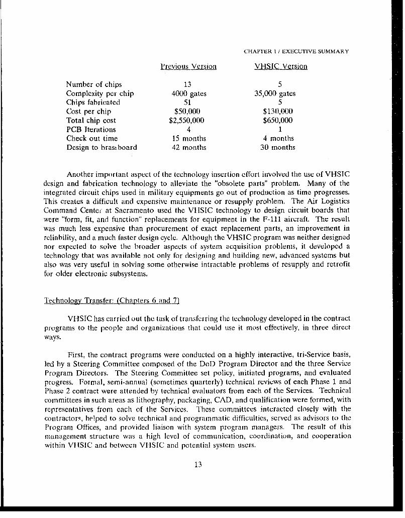
Two examples of the successful early insertion of VIHSIC technology into systems thathave passed the full scale development stage and are scheduled for production are theAN/APG-68 airborne radar signal processor by Westinghouse for the F-16 aircraft (scheduledfor 1991 production) and the AN/AYK-14(V) airborne computer by Control Data Corporation(scheduled for 1990 production). These are described in Sections 5.3.4 and 5.2.2 respectively.In particular, the AN/AYK(V) insertion proved that the benefits expected of VHSIC could infact be achieved in real systems, as the following table shows.
12
CHAPTER I / EXECUTIVE SUMMARY
Previous Version VHSIC Version
Number of chips 13 5Complexity per chip 4000 gates 35,000 gatesChips fabricated 51 5Cost per chip $50,000 $130,000Total chip cost $2,550,000 $650,000PCB Iterations 4 1Check out time 15 months 4 monthsDesign to brasstboard 42 months 30 months
Another important aspect of the technology insertion effort involved the use of VHSICdesign and fabrication technology to alleviate the "obsolete parts" problem. Many of theintegrated circuit chips used in military equipments go out of production as time progresses.This creates a difficult and expensive maintenance or resupply problem. The Air LogisticsCommand Center at Sacramento used the VHSIC technology to design circuit boards thatwere "form, fit, and function" replacements for equipment in the F-111 aircraft. The resultwas much less expensive than procurement of exact replacement parts, an improvement inreliability, and a much faster design cycle. Although the VHSIC program was neither designednor expected to solve the broader aspects of system acquisition problems, it developed atechnology that was available not only for designing and building new, advanced systems butalso was very useful in solving some otherwise intractable problems of resupply and retrofitfor older electronic subsystems.
Technology Transfer: (Chapters 6 and _
VHSIC has carried out the task of transferring the technology developed in the contractprograms to the people and organizations that could use it most effectively, in three directways.
First, the contract programs were conducted on a highly interactive, tri-Service basis,led by a Steering Committee composed of the DoD Program Director and the three ServiceProgram Directors. The Steering Committee set policy, initiated programs, and evaluatedprogress. Formal, semi-annual (sometimes quarterly) technical reviews of each Phase 1 andPhase 2 contract were attended by technical evaluators from each of the Services. Technicalcommittees in such areas as lithography, packaging, CAD, and qualification were formed, withrepresentatives from each of the Services. These committees interacted closely with thecontractorg, he!ped to solve technical and programmatic difficulties, served as advisors to theProgram Offices, and provided liaison with system program managers. The result of thismanagement structure was a high level of communication, coordination, and cooperationwithin VHSIC and between VHSIC and potential system users.
13
CHAPTER 1 / EXECUTIVE SUMMARY
Second, in order to increase the flow of information to potential users, the ProgramOffice set up a series of VHSIC Application Workshops to describe the products being
developed and the ways in which they could be applied in systems. Workshops for specialists
in technical areas such as CAD, packaging, and qualification were organized and held at which
information was exchanged, problems defined, and various approaches charted. More than
forty such workshops were conducted in all sections of the U.S.
Third, a number of major conferences were organized, the most prominent of which
were Annual VHSIC Conferences, held from 1982 to 1989. At these, the status of the total
program was presented to a wide spectrum of technical and management attendees from
Government and industry. Two VHSIC Tech Fairs were held at which the wares of most of
the VHSIC contractors were displayed and demonstrated. Technical VHSIC sessions were
organized at the Government Microelectronic Conference (GOMAC) fol the years 1978
through 1989.
An important indirect mode of technology transfer activity also took place. The very
existence of the VIISIC program and the visible results of its contract efforts spurred other
companies to initiate independent IC technology development programs with the intention of
remaining current and competitive. Several companies (including Raytheon in Phase 1 and
I larris in Phase 2) even entered into no-cost contracts with the Government in order mutually
to share information during their development activities. By the end of the VHSIC programthe list of companies that had gained a VHSIC capability included most of the major ICfabrication and/or design houses in the United States.
There were other indirect processes, such as the wide distribution of technical reportsand the development of DoD requirements documents, hy which VHSIC technology diffusedinto the electronics industry and into the procedures for the procurement of militaryequipment.
The Impact of VHSIC
VHSIC pursued certain specific goals in carrying out its program. ICs with fixedspecifications and electronic brassboards configured for particular weapon systems wererequired to be demonstrated. On the other hand, because of the broad utility of ICtechnology, the impact of VI ISIC activities and results could be equally broad and, therefore,difficult to measure. In order to assess the impact correctly one must, therefore, have a clearunderstanding of what VItSIC was expected to produce.
The fabrication goals of 1.25 and 0.5 micron feature sizes and the VFR goals of 5x10¹¹
and 1xl0 13 gate-IllTcm 2 wcre expected to he within the boundaries of the. then-current
development programs of the leading semiconductor companies. In fact, those were the
14
CHAPTER 1 / EXECUTIVE SUMMARY
conditions under which the development contracts were let. The expectation was that thesegoals would accelerate the emergence of technology that was already under active commercialdevelopment and hasten its application to military designs. In many cases these VHSIC goalsrequired the contractors to operate at the leading edge of their development efforts. Forexample, increased chip functionality required larger chip sizes which in turn required advancesin optical lithography, multilevel chip interconnects, and packaging technology. The reductionin feature size to 0.5 micron in particular put a heavy emphasis on the development of highresolution lithography using both electron beams and light optics.
Therefore, the specific chips that were developed during Phases 1 and 2 and used inapplication brassboards were primarily intended to demonstrate that a comprehensive masteryof the technology which met the stringent VHSIC requirements could indeed be achieved. Itwas also hoped that derivatives of these chips would find wide spread system application and,therefore, be required in increasingly large numbers. They would also be quickly absorbedinto the DoD acquisition process. This indeed did happen in some cases. In other cases thetechnology has evolved and diffused more indirectly so that the impact of VHSIC must belooked for beyond the bounds of the VHSIC hardware itself.
Chapters 2, 3, 5, and 7 of this report include articles on VHSIC that have beencontributed by people who were participants in the program or who have closely followed theprogram activity in a particular field of technology. The papers they have written are theirpersonal views of the impact VIISIC has had and include some descriptions of company-specific case histories by managers involved in VH-SIC contracts. The contributed papers alsoemphasize that many of the applications of VHSIC, especially in the design automation area,are ongoing and even accelerating. Therefore the impact of VHSIC in some areas will increasein time.
This Executive Summary concludes with one such assessment by the initial architect ofthe VHISIC program in his role as a former Director for Electronic and Physical Sciences inthe Office of the Under Secretary of Defense for Research and Engineering.
The Impact of VHSIC
Leonard R. Weisberg
Vice President, Corporate Research and EngineeringHoneywell, Inc.
The VHSIC program has had a profound impact on Honeywell's and othercompanies' technology and business strategies, and thus on the United Statesdefense capabilities. Besides greatly accelerating the use of new technology ICs in
15
CHAPTER 1 / EXECUTIVE SUMMARY
our military systems, VHSIC provided additional significant advantages includingthe VHDL language, high-speed multi-chip packaging, and interoperabilitystandards. Furthermore, ".he VHSIC program established, at Honeywell, a sourceof highly advanced radiation hard ICs for critical space and strategic applications.
Impact on DoD Systems
In order to maintain the U.S. technology lead, the use of new technology ICsin military systems had to be accelerated. Highly advanced ICs had to be availablefor military use at the same time they became available for the commercial market,or even earlier. Even though the military portion of the IC market had shrunk to7%, industry's attention had to be refocused onto military needs.
To accomplish this, a very different kind of program was needed. VHSICwas established with strong DoD policy support and unprecedented funding levelsfor a broad technology research and development program. VHSIC focusedattention not only on advancing the IC technology, but also on special militarysystem requirements including ultra-high speed processors for which thecommercial demand is limited.
The VHSIC program galvanized the semiconductor IC industry into action.Several of the largest IC manufacturers became contractors or subcontractors in theVHSIC program including IBM, Motorola, TI, and National; it is noteworthy thatthe last three are presently among the top five producers of military ICs. Similarly,VHSIC became the focal point of attention among the top military contractors forelectronic 5ystems and subsystems, with Westinghouse, Hughes, TRW, andHoneywell as main contractors in VHSIC.
The VHSIC technology goals were symbolized by the numbers 1.25 micron("near-micron") and 0.5 micron ("submicron"). These numbers set new,demanding goals for the production of military ICs at both merchant ICmanufacturers and system developers. Achieving submicron dimensions was nolonger a distant goal, oriented mostly to commercial memory requirements.Instead, it became a real target whose achievement would ensure a leading businessposition for those companies that reached it.
As a result, the VHSIC contractors built up their IC capabilities withinvestments estimated at double (or more) the VHSIC funding. For example,Honeywell invested about $300 million, nearly triple its total VHSIC contractfunding. Even companies that did not have VHSIC contracts felt that they had toremain competitive and therefore also significantly increased the investment in theirmilitary IC capabilities.
It is our estimate that near-micron and submicron military ICs have becomeavailable to the designers of military systems three to five years earlier than wouldhave happened without the VHSIC Program. Military systems and equipment arenow in development with these advanced ICs, or their direct derivatives, which giveunprecedented performance, size, weight, power and reliability that could not havebeen achieved without VHSIC.
There are now over 40 programs in which VHSIC has been or is beingdesigned into future prodtict-. In Honeywell alone, these include the Enhanced
16
CHIAPTER 1 / EXECUTIVE SUMMARY
Modular Signal Processor (the new Navy standard processor), the MK-50Advanced Lightweight Torpedo, the Advanced Spaceborne Computer Module, theMultipurpose Space Computer, and upgrades to Milstar.
ImFact on Technology
Besides meeting the main VHSIC goal of accelerating military IC capabilitiesby three to five years, other important capabilities emerged tr'on, the VHSICprogram of significant importance to industry.
VHSIC Hardware Description Language (VHDL)
The development of VHDL is particularly notable. The VHDL portion of theVHSIC program was a far-sighted endeavor with an outstanding payoff. It is nowpossible to start an IC design at a functional system-level description, proceedinto more and more detailed design levels and end up with a fully documented andwell validated circuit layout ready for fabrication. This is all done under thecontrol of a computer aided design (CAD) system. It significantly reduces thetime and cost of the design by virtually eliminating the need for major redesign.
VHDL has been established by the IEEE and accepted by industry as astandard language for the description of ICs. It will reduce the cost of ICprocurement by providing better documentation of design specifications. It willmake second sourcing much easier, allow designers to mix and match ICs fromdifferent vendors in their designs, and alleviate the perennial problem ofreplacement of obsolete IC parts.
Multi-Chip Packaging
It has long been recognized that shrinking the feature sizes on the IC chipis not a complete solution to the need for increased electronic functionality. TheIC chips themselves need to be more densely packaged in order to increase thespeed of interchip data exchange and achieve further reductions in size and weight.The development of thin film multi-layer (TFML) multi-chip IC packaging underthe VHSIC program was again a far-sighted development.
Interoperability Standards
The VHSIC program has helped in the establishment of standards forinterfaces between chips on a board and between boards, and for test andmaintenance buses. As these standards become broadly established and used innew designs, the circuits developed by different contractors will be able to operatetogether compatibly and built-in or self test becomes more practical and cost
17

CHAPTER 1 / EXECUTIVE SUMMARY
effective. The Vi1SIC standards form the basic foundation of the common moduledevelopments which have become increasingly important in the design of militaryavionics systems.
Impact on Honeywell
The impact of VHSIC on Honeywell is probably similar to those of the otherVHSIC contractors and can be viewed as a typical case history.
By 1980, Honeywell had established a major IC capability oriented mostlyto internal needs. This was not unusual for companies with a major computerbusiness. Special ICs were required and, before the advent of silicon foundrycompanies, total dependence on independent vendors for the development anddelivery of the needed ICs was considered to be too risky. Some very specializedproducts were also needed and these could most easily be held as proprietaryproducts with an internal facility. However, maintenance of such internal facilitieswere (and are) expensive and becoming more so as the IC technology rapidlychanged.
When the VHSIC program was first announced, it was recognized thatparticipation in the program would require a major change in the company'sbusiness strategy for ICs. Winning a VHSIC contract would mean operating underDoD specifications and restrictions and losing some proprietary advantage. On theother hand, it would accelerate the technology advances already under way in thecompany and would potentially provide a stronger and more responsive capabilityfor its military business.
To respond to the VHSIC challenge, Honeywell formed a new programorganizatio', and a new plan for technology development was put in place. Forexample, a program on CAD (computer aided design) underway in one of thecomputer divisions was accelerated by nearly two years to meet the VHSICprogram needs. Major corporate investments were made for both new equipmentand facilities. People at all levels worked long and hard on the VHSIC programto make it a success.
One particular result was that Honeywell combined its new VHSICtechnology with ongoing efforts on radiation hard ICs. This provided a nowgeneration of radiation hard memories, gate arrays, and processors withoutstanding performance, size, power, and reliability for space and strategicapplications.
This, VHSIC created in Honeywell both a major new technology capabilityand a major new source of supply for military ICs. Without the VHSIC program,this capability would not exist.
Conclusions
The VHSIC program has had profound effects on military ICs, changing theindustry and advancing the technology and product availability by several years.The full impact of the VHSIC program may not be seen for a few more years
18
CHAPTER 1 / EXECUTIVE SUMMARY
during which the many systems now in development are deployed. The VHSICprogram has had a positive and decisive role in making these systems possible.
19
Table 1.1 - Major Events, Milestones, and Highlights
1978 o I)oD letter of instru-tion to the three Services culminating the period ofprogram concept discussions in Dol) (July 19)
o Program "kick-off' meeting in DoT), chaired by Mr. L. R. Weisberg; formationof Overview Committee and technical working committees for lithography,fabrication, and DAST (Design, Automation, Software, rest) (August 9)
o Extensive organi';ational, policy, and technical meetings within the Governmentand with industry to define the program in detail (August 1978 - April 1979)
1979 o Mr. L. W. Sumney appointed first VIISIC Program Directoro New line items for $12M per Service established in FY80 budget (January)o Formulation of procurement procedures (February - March)
o Commerce Business Daily Announcement #117, describing the VttSIC program(April 15)
o RFP for Phase 0 - Program Definition issued (June 22)o REP for Phase 3 issued (November)
1980 o Phase 0 awaids (9 contracts, $10.5M): (March)Hughes, Rockwell., GE (Army)TRW, IBM, Westinghouse (Navy)T.I., Iloneywell, Raythcon (Air Force)
o Phase 3 contract awards (April - October)o Phase 1 RFP issued (September 10)o Phase 0 completed (December)
1981 o Phase 1 contracts ($167M) started (May 1)I lughes, T.I. (Army)IBM, TRW (Navy)Hloneywell, Westinghouse (Air Force)
o First Annual VIISIC Review and program kick-off meeting (June)
1982 o Mr, F. D. Maynard, Jr. appointed VIISIC Program Directoro Technology Insertion studies begun
1983 o Fifteen weapon systems selected for Technology Insertiono First fully functional VIISIC chip - TRW Matrix Switch (Febru! -y)o Nine contracts awarded for Submicron Program Definitiono Yield Enhancement program definedo Manufacturing Technology program( definedo VI ISIC I lardware Dcscription Language (VI IDL) development began with one
year program definition phase (July)
20
CHAPTER If EXECUTLVE SUMMARY
198'4 o Yield Enihancemnent nmodificat ions to Phiasze i contiacts executedo Acoustic signal processor using. VI ISIC chip demnonsirated by IBM (May)o Integratcd Design Automnation Systemn procurement startedo VI IIL information releasceO from ITAR control (January)o Phase 2 contract awards (Novermher'l to
I11M (Army)TRW (Navy)Hloneywell (Ah Forcc)
o Additional Technology Insertion candidates selected
1985 o Yield Enlhancemcnt and %lanufacturing Technology programs startedo Information oin Bus Intcifacc Unit released from ITAR control (August)o Elc op cSignal Processor brassboard demonst rated by IHoneywell
(September)o VI IDL Support Environment information released from ITAR control
(Octobcr)
1986 o VIISIC TISSS information '-ased from ITAR control (Junie)o First systemi demonstration ot VI-SIC technology: AN/ALQ-131 electronic
wvarfare pod with TRW Phase 1 chips flight tested at Eglin AFB (July),o MIL-STD-1750A comiputer 1-ras,;boarcl using VI-SIC chips demonstrated by
Texas Instruments (Juily)o Navy flight dIemonstration of 113M VI ISIC Signal Conditioner for the AN/UYS-
I it, a P-3 aircraft, kSeptcmiber)o AE13LE-150 electron beam lithography ma'"line delivered to Motorola for use
in the Phase 2 (October)o Dernovstrat ion of VI ISIC chip set in thc Enhanced Position Location and
Reportinig System by H ughes (Decenmhcr)
ofnt litl fully- functional VI ISIC. chip types fabricated with total productionofVIISIC chips over 100,000 (IDecember)
0 Phase 2 cuiiti actov establish chip ijitelopei ability specificatiOii
1987 o, V1 ISIC version of the F-I 11 D igital Signal Transfe- Unit demonstrated in flighto VIISIC chip packaging information releasý-d from ITAR control (March)
oNavy AN/SRS- 1 Combat 1)/F system wtith VI ISIC chilps demionstrated by SandersAssociates (Septcnibc')
Co VI IS! (Circuijt boar1dS With I loneywel I chips demonstrated in Navy AN/UYS-2Fifihanced Modul-ir Signal Processor (Scptebhe& )
0 VI ISIC automa11tic tartget tracking systemi with I Iughics chips for the MIAl tankdemiorst rated (De)ceniber)\ VI ISi( I b'rdware lDem~rlption Languiage (VI IDL) adoptt_-d for industry widedc"Ifp ,1i 1 i~ca 1FF IFT Stofndard 17i ThIcebr1t
CHAPTER 1 / EXECUTIVE SUMMARY
1988 o Dr. J. M. MacCallum appointed VHSIC Program Directoro ADAS in-)rmation rele-ed from ITAR control (March)o VHDL documentý,,ou mandated by DoD for all new systems (September)o Complex vector proc.isor module for Advanced Tactical Fighter demonstrated
by Westinghouse (November)o Demonstration of Phase 2 radiation hard 0.5 micron chips in an anti-submarine
warfare beamformer brassboard by IBM (December)o Insertion of Phase 2 VHSIC technology into cruise missile advanced guidance
unit begun by Honeywell and General Dynamics
1989 o Demonstration of a fully functional CPUAX superchip designed by TRW andfabricated by Motorola; running at 12 MHz (December)
1990 o General Dynamics demonstration of Honeywell Phase 2 chips in brassboard ofcruise missile advanced guidance unit (scheduled for September)
22
CHAPTER 2 - THE VHSIC PROGRAM HISTORY, STRUCTURE, AND POLICIES
2.1 Program Origins and Objectives .................................. 24
The Legacy of VHSIC - Larry W. Surn ey ........................... 26
2.2 Program Structure . ............................................ 302.2.1 Phase 0 - Concept Definition . ............................... 302.2.2. Phase 1 ....... .......................................... 322.2.3 Phase 1 Yield Enhancement . ................................ 342.2.4 Phase 1 Te.chnology Insertion . ............................... 352.2.5 Phase 2 Submicrometer Technology Development ................ 352.2.6 Phase 3 and Other Supporting Technologies .................... 372.2.7 D esign Autom ation . ...................................... 382.2.8 VIISIC Manufacturing Technology Program - Joseph A. Key ........ 39
2.3 Program M anagement .. ......................................... 40
2.4 Funding .. ................................................... 42
2.5 Security - Jam es .1. Hower . . ..................................... 422.5.1 1listory of VIISIC Security M easures ......................... 422.5.2 Additional Security Decisions . ............................... 47
23
CHAPTER 2
THE VHSIC PROGRAM - HISTORY, STRUCTURE, AND POLICIES
Yery High Speed Integrated Circuits (VHSIC) is the name of the program which theDepartment of Defense program conducted over a period of more than ten years beginningin March 1980. Over this period of time, the objective of the program was to develop twonew generations of the silicon integrated circuits for use in DoD weapon systems.
This final report on VHSIC summarizes the background and origins of the program,its structure, and the contract efforts undertaken to accomplish the program objectives. Italso covers the accomplishments made during this period, the activities of DoD laboratoriesin support of the contract efforts, and an assessment of the impact that VHSIC has had oil thetechnology of the integrated circuit and its use in military equipments.
2.1 Program Origins and Objectives
The defense posture of thý, Unized States has been increasingly based upon the conceptof a military force that is technologically superior to any potential adversary. We useadvanced technology, particularly electronic technology, wherever possible to ensure ourability to defend against numerically grcater forces. In any modern electronic system thesilicon integrated circuit is the basic device for processing signals and it has becomeindispensable in the design of modern military weapons. The technology for making thedevice is a very demanding one. Complex and expensive equipments are required to produceit, advanced skills and knowledge are required to use it, and large continuing investments arerequired to keep it up-to-date.
During the 1960s, the DoT.) was the leading world force behind the development ofintegrated circuits (ICs). It supplied much of the research and development investment andaccounted for over 70% of the user market in the United States. It was, therefore, able tomaintain a coml'ortable lead in the military applications of ICs. During the 1970s, thecommercial exploitations of this new technology grew very rapidly and resulted in a largeexpansion of commercial sales, By 1978, even though the DoD use of microcircuits had itselfgrown substantially, commercial applications represented more than 90% of the totalintegrated circuit market sales,
As a result, the WC manufacturers became oriented toward the large commercialmarket and less interested in supporting military requirements. Through law, regulation, andtpolicy, the [o)oD's limited buying power was further diluted by fragmented purchasing patternsacross the industry. The "comfortable lead" of the U.S. in the military applications of ICsbegan to erode.
The DoD, concerned about this change, spent several years carefully assessing its nccdsarnd deficiencies in thi,; qrea of to.chr•olgy he r'nor deficiency perceived was that too often,military microelectronic products did not incorporate the state of the art technology used in
24

CHAPTlER 2 / HISTORY, STRUCTURH, AND POLICIES
commercial products. Advances in the semiconductor industry were not focused on militaryapplications and most chips had to be separately qualified on low volume manufacturing linesto meet military specifications after their qualification for the commercial market. A gapresulted between the commercial introduction of advanced technologies and their use inmilitary systems. Worse still, the delay was increasing with time. By 1980, this time lag hadgrown to 10 years or more for many DoD systems.
Using commercial products could not solve the problem because their performance didnot generally meet military system needs, especially in the environmental areas of temperatureand radiation. Compounding the pioblcm was the fact that weapon systcems were becomingincreasingly dependent on electronic subsystems for their effectiveness, speed of response andadaptability to changing battle environments. There was also increasing evidence that Sovietweapons systems were beginning to use sophisticated integrated circuits.
Based on these considerations, the DoD decided to correct the deficiency by givngsystem developers and acquisition managers a military qualified microelectronics technologythat was on par with the technology available commercially. It established the program calledVHSIC, with the objective of being able to design, manufacture, and use silicon ICs inmilitary systems with state-of-the-art fabrication technology, i.e. concurrently with commercialproducts.
After a number of discussions between Government and industry representatives, thetechnical goals of one-half micron feature size and 100 megahertz clocking frequency werechoseen to quantify the desired product. IC chips combining these two characteristics wouldimply the ability to process electronic signal much more effectively than the technology cur-rent at that time. A figure of merit called the functional throughput rate (FTR) with unitsof gate-hertz/cm 2 was devised, which incorporated chip area, clock speed, and complexity (asmeasured by the number of electronic logic gates) into a set of desired attributes. One couldthus characterize the suitability of IC chips for various applications.
At the same time, it was realized that these ambitious goals could only be reachedafter prolonged development efforts. Therefore, an additional "mid-term" goal of 1.25 micronfeature size and 25 megahertz clock speed was chosen. This goal would be less difficult tomeet but would still represent a significant advance in technical capability. It would alsolessen the risk of the program and, if necessary, provide a decision point midway through theprogram on whether to proceed or not.
During the preparation of the VHSIC program plans, it was evident that. many of thedetailed technologies involved in IC design, fabrication, and use were sufficiently new that asupporting research and development effort in these areas was needed in order to reduce therisk of reaching the end goals. This supporting cffort should also be separate and independentof the main line of development.
It was also ::lear from the start of the planning that the wide spectrum of capability inthe U.S. semiconductor industry, and the equally wide technical approaches possible towardachieving the program goals, would make it impossible for the Government by itself to definethe detailed tasks necessary lo initiate a full scale development program. The DoD wouldneed closc interaction with industjy in putting the pirugiam intoi action. It decided to do thisby means of a concept definition phase in which many contractors would be funded to study
25
CHAPTER 2 / HISTORY, STRUCTURE, AND POLICIES
the problems posed by the VHSIC goals and to describe in detail their approach to solvingthem.
The following assessment of the impact that VHSIC has had on the semiconductorindustry and the technologies used in it, has been contributed by the first Director of the DoDVHSIC Program Office. As such he had the initial responsibility for formulating and carryingout the plans for getting the program started.
The Legacy of VHSIC
Larry W. SumneyPresident, Semiconductor Research Corporation(Former Director, DoD VHSIC Program Office)
Introduction
Eight years have passed since my association with the VHSIC program. Inthese years, I have continued to work closely with the semiconductor industry ofthe U.S. but in an environment not dominated by the strictures of government.This permits easier decisions, more rapid implementation, and greater cooperationthan is possible in Government programs such as VHSIC, and provides an excellent
technology and management perspective for evaluation of the impacts, products,and lessons that constitute the legacy of VHSIC.
Quoting from an earlier description of the VHSIC program, 1
"...the purpose of VIISIC is to apply a constructive bias to the direction of thedefense technical establishment and to the semiconductor cohmaunity so as toprepare them .or a radically altered fiture, and to increase both the ability anddesire of the inilustr y to respond to the Nation's defte/1' needs. In the processof achieving this larger goal, and in order to achieve it, specific VLSI chips willbe made, demonstrated, and applied in current vital defense systems. In addition,DoD nianagement innovations are being tested that will permnil more productivity
for generic research and techlnology ini'estments."
By this goal, VHSIC can only be viewed as a success. Defense technology hasbeen converted to the VLSI age and semiconductor manufacturers are veryresponsive to defense needs. Complex chips have been made and demonstrated,and management innovations have been applied successfully. As with most major
Suwnriy, L.W., "VW SI(: A Stitus Report", I EEL Spectrum, pp. 3.1-39, Decerntcr 1982
26
CHAPTER 2 / HISTORY, STRUCTURE, AND POLICIES
programs, the objectives were defined in different ways by different people. VHSIC
certainly did not succeed in meeting every objective defined for it. It has even
been criticized for not meeting objectives that were never defined. But for those
objectives defined either contractually or in policy statements, the return on DoD's
investment of funds and hard work has been gratifying and substantial. I will
illustrate with some of the more important ones.
Industry Teaming
At the 1987 VHSIC Tech Fair, Dr. William Perry, a former Undersecretary of
Defense for Research and Engineering, expressed disappointment that VHSIC had
only partially succeeded in integrating the efforts of merchant semiconductor
companies and defense system contractors. I take an opposite view. Inhibited by
competition, the usual adversarial habits of U.S. companies, or perhaps by the
legacy of anti-trust actions, U.S. companies have, for many years, had difficulty
in identifying ways to work together constructively. The team building established
as a requirement of VHSIC at first was forced but, under the severe demands of
the program, developed into strong cooperative relationships. The demonstration
that such cooperation can work in this country has made it easier to implement the
cooperative endeavors required for U.S. industry to effectively compete in
international markets and has provided the pattern for future teaming arrangements
that are now very common. Of course, not every teaming relationship worked andperhaps not as many were even proposed as we would have liked, but even for
those that did not work, I believe that better understandings developed and overall
benefits have accrued.
VHDL
In 1980, as VHSIC was beginning, the cost of designing a silicon chip was
between $100 and $200 per gate. The design of a 20,000 gate chip could entail an
investment of over $2 million and require over 2 calendar years. These costs were
prohibitive for the broad system applications contemplated by VHSIC planners. It
was even suggested 2 that complexity was advancing to the point that designmight become impossible and that design tools for VLSI did riot exist. The
reductio. dcnd simplification of complex chip design through the invention of
automatic design tools became a major focus of the VHSIC contractors.
The VHSIC hardware description language (VHDL) is a majcr output of this
design effort. It provides a common computer language which is applicable at
various levels of design as well as in testing, specification, procurement, and
logistics functions. VHDL has become an official IEEE standard (IEEE 1076) and
is now a widely used standard for design.
2 Robinson, A.L., Arc VLISI Microcircuits ',o I Isrd( "o I)csign?'", Scicnice. Vol. 2(9, p. 258, 1980.
27
CHAPTER 2 / HISTORY, STRUCTURE, AND POLICIES
VHDL is just one of many advances in the design area that resulted from theVHSIC program. Today, design automation has advanced to where the cost pergate for some designs is under $1, a two order of magnitude reduction in costmaking VHSIC chip design affordable. A significant portion, but by no means all,of this improvement is attributable directly to VHSIC. A major contribution to theU.S. microelectronics industry was made. Computer aided design remains one ofthe few strong assets of this vital U.S. industry.
Chips
Many chips were developed by the VHSIC contractors and probably just asmany by companies who chose to develop their own VHSIC capabilities. Some ofthese are now being tested, applied, and integrated into systems. Others have notfound application. Many VHSIC chips were developed by companies not fundedby the program but who were spurred by VHSIC to develop their own competitivetechnologies. The results are a large standardized set of VLSI chips designed andavailable for application in military systems. Their actual insertion into militarysystems has not been rapid due to the endemic system development cycle fordefense systems that takes ten years and is difficult to change. This is a largerchallenge than the VHSIC program was designed to address.
To cite one example of an outstanding VHSIC chip, the "superchip" developedby TRW and Motorola in Phase 2 of the program was demonstrated in December1989, as a proof of concept device at the very state of the art in either defense orcommercial technology. It contains 4 million devices, is capable of 200 million 32-bit floating point operations per second, consists of 142 macrocells (each one ascomplex as a normal chip) that can be externally reconfigured, uses 0.5 micronCMOS technology, and is designed for use in advanced signal processingapplications. The superchip is the first of the new generation of complex chipsthat will set the leading edge of the technology for the next generation of VLSI.It has created a challenge to which others will respond. It is a direct product ofthe VHSIC program.
Computers
At the 1989 IEEE Workstation Symposium, a desktop supercomputer wasdemonstrated by the Johns Hopkins Applied Physics Laboratory. Designed forapplications in computer visualization and capable of over I million computationsper second, it uses low cost chips in a parallel processing architecture andrepresents the current state of the art in workstation technology. It was developedusing VHSIC technology almost exclusively and represents one of the firstcommercial applications of VHSIC technology.
28
CHAPTER 2 / HISTORY, STRUCTURE, AN1) POLICIES
Lithography
Lithography, the process by which microcircuit patterns are transferred from thedesign station to the silicon, wafer, is perhaps the most critical of all semiconductortechnologies because of its key role as the pacing technology. VHSIC led in thedevelopment of the vital electron-beam machine that writes the patterns on amask and assisted in the development of the next generation optical steppers andX-ray machines that transfer the mask patterns onto the wafers. These tooldevelopment efforts have resulted in the continued availability of critical tools fromU.S. manufacturers even as the U.S. industry's share of the world market forlithography tools has deteriorated badly. Each of these areas are now beingaddressed by SEMATECH. Without the VHSIC activities in lithography, therewould most likely be no industrial base in this technology area for SEMATECH tosupport.
Commercial VLSI Technology
One of the principal reasons VHSIC was initiated was to leverage the significantadvances of the U.S. commercial industry for military applications. DuringVHSIC's lifetime, however, our commercial industry stumbled as it facedinternational competition. So, although the impact of VHSIC on U.S. commercialintegrated circuit manufacturers has been discounted because this was neither theintent nor the thrust of VHSIC, in fact, significant VHSIC resources were directedto merchant semiconductor manufacturers who found that the VHSIC goals reachedbeyond their commercial objectives. It caused them to accelerate the pace of theirtechnology development. Several years before the VHSIC program started, it waswidely believed that half-micron semiconductor technology would not becomeavailable before the turn of the century. Now, at least partially as a result of theacceleration of technology development by VHSIC and of the clear annunciation ofVHSIC technology goals, the half-micron technology is on the verge of broadcommercialization.
Conclusions
From the perspective I have, VHSIC is an outstanding success for which theDoD should take great credit. It has advanced both the defense and commercialtechnologies in the U.S. semiconductor industry, made design and fabrication toolsavailable that would not have otherwise existed at this time, and accelerated ICdevelopments in the U.S. industry. That it has not solved the major defensesystem development cycle challenge nor the competitiveness problems of the U.S.commercial semiconductor industry is not surprising. It was neither intended,directed, nor funded to do either. In the context of the actual intentions and goalsof the DoD VHSIC Program, it has been an outstanding success.
29
CHAPTER 2 / HISTORY, STRUCTURE, AND POLICIES
2.2 Program Structure
The program structure that evolved from all of the technical and administrative factorsthat had to be considered initially included four major phases. At various later times, certainareas of activity in these phases became separately identified. The final resulting programstructure is described below. Each program phase was carried out by contracts awardedcompetitively. For each contract, Appendix B lists the contractor, the contract title andnumber, and a reference to the final report if available.
The VHSIC program was structured to address the following general technical issues.
o ICs with greater functionality and higher speed would require a longer, morecomplex, and more costly design cycle.
o Greater functionality would require either larger area chips or smaller featuresizes (or both) in order to accommodate a larger number of transistors. Thiswould result in longer chip development time and higher manufacturing costs.
o Military ICs had to meet stringent requirements for radiation hardness, lowpower consumption, and high reliability over a wide temperature range. As thecomplexity and size of the chips increased so did the difficulty in meeting theseenvironmental conditions.
o High reliability, in turn, required the development and use of fault tolerantdesigns and built-in self-test (BIST) circuits in addition to a well disciplineddesign and manufacturing technology.
2.2.1 Phase 0 - Concept Definition
Phase 0 began in March 1980 as a nine month effort during which the contractorsconducted intensive preliminary technical studies and then defined a detailed developmentprogram to accomplish the technical objectives set out by the VHSIC program office. Thenine companies that participated in Phase 0 were General Electric, Honeywell, Hughes, IBM,Raytheon, Rockwell, Texas Instruments, TRW, and Westinghouse.
As guidance during the Phase 0 studies, the VHSIC Program Office required that thefirst phase of VItSIC technology meet certain minimum specifications which were chosen tobe a reasonable compromise between the ultimately desired chip performance and thedifficulties that were expected in developing the necessary technology. The desiredperformance was expressed as goals for the contractors to aim at. The specifications areshown in the table on the following page.
30
CHAPTER 2 / HISTORY, STRUCTURE, AND POLICIES
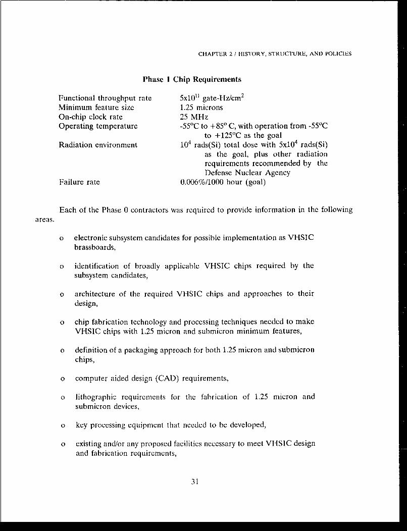
Phase 1 Chip Requirements
Functional throughput rate 5x10" gate-Hz/cm 2
Minimum feature size 1.25 micronsOn-chip clock rate 25 MHzOperating temperature -5511C to +85" C, with operation from -55'C
to +125'C as the goalRadiation environment 10 4 rads(Si) total dose with 5x10 4 rads(Si)
as the goal, plus other radiationrequirements recommended by theDefense Nuclear Agency
Failure rate 0.006%/1000 hour (goal)
Each of the Phase 0 contractors was required to provide information in the followingareas.
"o electronic subsystem candidates for possible implementation as VHSICbrassboards,
"o identification of broadly applicable VHSIC chips required by thesubsystem candidates,
"o architecture of the required VHSIC chips and approaches to theirdesign,
"o chip fabrication technology and processing techniques needed to makeVHSIC chips with 1.25 micron and submicron minimum features,
"o definition of a packaging approach for both 1.25 micron and submicronchips,
"o computer aided design (CAD) requirements,
"o lithographic requirements for the fabrication of 1.25 micron andsubmicron devices,
"o key processing equipment that needed to be developed,
"o existing and/or any proposed facilities necessary to meet VHSIC designand fabrication requirements,
31
CHAPTER 2,/ HISTORY, STRUCTURE, AND POLICIES
"o support environment, such as a higher order language for use in DoDsystems, which would simplify the use of VHSIC,
"o approaches to providing increased reliability and testability of VHSICdevices,
"o procedure for making VHSIC products available for sale to all otherDoD contractors and government laboratories,
"o procedure for making major equipment developed available to otherDoD contractors and government laboratories, and
"o corporate strategy for rapidly introducing VHSIC into DoD systems.
The study programs were completed in December 1980. Based on the work duringthe Phase 0 contracts, each company submitted a proposal to the Government for Phase 1,emphasizing the development of 1.25 micron technology and a brassboard which woulddemonstrate the advantages of its application in systems. Final technical reports for each ofthe Phase 0 contracts are listed as References 2.1-2.9.
2.2.2 Phase I
In May 1981, Phase 1 started with major emphasis on the development and pilotproduction of silicon chips with 1.25 micron minimum feature sizes, their demonstration insubsystem brassboards, and a minor exploratory effort on submicron technology. The twotechnical development efforts were separately designated as Phase la for the 1.25 microntechnology development, and Phase lb for the submicron technology feasibility study. ThePhase 1 contracts were awarded to six major companies, or teams, with expertise in weaponsystems development and semiconductor manufacturing. The contractors were Honeywell,Hughes Aircraft, IBM, Texas Instruments, TRW, and Westinghouse. The detailed contractrequirements are given in Reference 2.10 and the final reports are References 2.11-2.15.
Phase la
The goal of Phase la was to develop the necessary processes, tools, and designenvironments for tiLc prodluction of 1.25 micron signal processing chip sets that would performreliably in severe military environments, be affordable, and be usable in a wide variety ofapplications. This goal supported the key DoD objective of sign)ificantly reducing the delayin getting advanced semiconductor technology into fielded military systems. The technical
..r.i ..e..ents for the IC chips c 4...... ... t 1 i were thc same as thosc listd above forPhase 0 (Concept Definition).
32
i~~ I=modII I I I I I I
CHAPTER 2 / HISTORY, STRUCTURE, AND POLICIES
Phase lb
The goal of Phase lb was to develop a 0.5 micron VHSIC technology and to fabricatetest chips which demonstrated that the design and manufacture of VHSIC chips on a pilotproduction basis would be feasible during Phase 2. In attempting to meet 0.5 micron goals,all critical problems were to be identified and specific methods of approach for their solutionwere to be addressed. The technology developments needed in order to meet the VHSTC endguals of 1013 gate-Hz/cm 2 FTR with a minimum on-chip clock rate of 100 MHz were to beaccomplished in Phase lb.
In order to overcome the increasing limitations of conventional optical lithography ofpattern features in the submicron range, a separate additional contract was awarded toHughes Aircraft for the development of an electron beam lithography machine capable ofpatterning 0.5 micron circuits suitable for use in large scale manufactuti lg operations.
The specific tasks to which all of the Phase 1 contractors were committed were groupedinto four principal areas and summarized as follows.
Chip technology and fabrication
"o Develop a 1.25 micron baseline process to fabricate VtISIC circuits.
"o Establish a pilot production line to supply the projected number of VIISICchips needed.
"o Supply chip packages which meet the military environmental conditions, as wellas the performance requirements such as speed, input/output connections, andpower dissipation.
Design, architecture, software, and test
"o Develop an architectural approach and design methodology which supports theVHSIC performance requirements.
"o Provide software development systems at a high order language level, preferablyusing Ada.
"o Include provisions for on-chip self test and fault tolerance at the chip or modulelevel.
33
CHAP'ER 2 / HISTORY, STRUCTURE, AND POLICIES
o Define the CAD tools needed to support the full spectrum of the design processfrom architectural specification to physical chip interconnection and layout.
"o Develop a simulation methodology to validate circuit, chip, and subsystemdesigns and to project performance accurately before fabrication.
Chip and subsystem design
"o Carry out a detailed system analysis to define the VHSIC subsystem designrequirements.
"o Develop specifications for th&; VIISIC modules, chips, and functional macrocells.
"o Design and layout the VIISIC chips and modules needed for the brassboard,including provision for testability and fault tolerance.
"o Demonstrate the completed brassboard in simulated operational conditions.
Technology transfer
"o Provide an effective plan for making chips, design services, equipment, andsoftware available to other DoD contractors.
"o Establish a plan for developing a second source of supply for chips.
"o Prepare a plan for insertion of the VHSIC technology into DoD systems.
2.2.3 Phase 1 Yield Elnhancement
In order to demonstrate the advantages of VIISIC technology in technology insertionprojects a substantial supply of chips was needed. Because new fabrication techniques wereused in the VHSIC pilot lines, the chips initially produced on the lines were sufficientlyexpcnsive to discourage large scale use. The goal of the yield enhancement (YE) program wasto ensure the supply and affordability of the VIISIC chips by increasing the pilot lineproduction yield and by cstablishing a more disciplined production environment. The causesof low yield needed to he identified and corrected.
Industrial cxperience shows that the chip yield for a givel, rcCess increases as theamnunt of product processed through the line increases. This is the "learning curve'phenomenon normally encountercd in all production line systems. Therefore, a substantialamount of wafer processing was one of the requirements of the YE program. Progress in
34
CHAPItR 2 i HISTORY. STRtUCTURE, AND) POLICIES
achieving improved yield was macasured by periodically starting the fabrication of three
consecutive lots of wafers that •werc collcctively called a Yield Vcrification Run (YVR). Each
coritractor had a goad tol yield which the pilot line should achieve by the end of the progi am.
2.2.4 Phase I "lcchnolog* unsertion
"Technology Insertion" is the term used to describe the application of the produc.tsdevclopcd under the VlISI(. programn to (he d,:sign and acquisition of systems. Technologyinsertion constituted one of thle bhasic goals of the VI ISIC program. Since hardware insertionnecessarily involves the linkitig of "high tcch" with opcrational militalry systems, it was also oneof the more diffiCUIt problems that confronted the VIISIC program managers.
The Vi IS;C program1 aipproat:h to, rmectint" Ihis challclng was to support a substantial
i1uilbcr of system hardwarc inscertion projccts. The projects supported the use of VIISICchip!, in both existing. fielded .systemns and others still under development. In cooperation with
s,,stcm program offices VI ISIC co-tunded bhoth feasibilitv studies and hardware insertion into
opcra!ling systems, to demonstrate that VIISIC worked and that its use was beneficial. The
benefits becatme m1anifest in diffcrcnt ways depending on the application --- increased
performance, increasud rlicability, collanced maintainability, reduced acquisition costs, less
weight and space, or reduced life cycle costs. At least twenty-seven major system insertionefforts wcte underitaken in ,hich the use of VI ISIC technology derno.istrated the potential for
improved system perfornmricc. In somne ca)ses such as the Ar.wys Firefindcr radars and the
joint Nav.%,/Air Foice I1 W.'i-l IF communications terminal, the projected saving in system life
cycle costs approached the total cost of the VI ISIC program.Therc wcre ;also at number of independent insertion programs in the systems
applications area. TIhey uscd the advanced VIlSIC microelectronic hardware in system
devclopments but, since they were not directly funded by the VI ISIC Program Office, they are
no' dcscrihed in this report.Collectively, these VI IS IC technology insertion efforts reflected the growing activity by
I),'I contractors anld by the commercial elcctronics industry in introducing VHISIC products
and technology into milit1lry systems.
2.2.5 Phase 2 Stlmicronlwer ITechnoigy IDevelopnent
"1hC P]hise 2 subinici on goal wams to dcvclop a sccond( gcncration of silicon chips
charactcrizcd by 0i.5 micron feature sizes and a clock frequency of 100 MI-Iz. Phase 2 was
.ct'cdcl( by anothcr pro)gi a ) defii it ion study (Pha.tse 0') similar to Phase 0, in which detailed
atppioaches io the 01.5i micron goal wVCle developed in(] proposed by nine contractor teams
licadtid by I l•a•is, I hc':ywell, I lughcs. IBM, RCA, lexas InstrutmCnts, TRW, Westinghouse,":nd Western I:,lect ic.
-the nieC I'hbase 0' contractors finished their stuidy programs in January 1984 and
suthinilt Cd proposals in rcspo,',sc to the RIT1! is,,tltcd for Phase 2.' The final reports for Phase
35
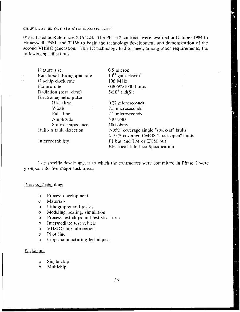
CHAPTER 2 / HISTORY, STRUCTURE, AND POLICIES
0' are listed as References 2.16-2.24. The Phase 2 contracts were awarded in October 1984 toHoneywell, IBM, and TRW to begin the technology development and demonstration of thesecond VHS1C generation. This IC technology had to meet, among other requirements, thefollowing specifications.
Feature size 0.5 micronFunctional throughput rate 1013 gate-Hz/cm 2
On-chip clock rate 100 MHzFailure rate 0.006%/1000 hoursRadiation (total dose) 5x10 4 rad(Si)Electromagnetic pulse
Risc timc 0.27 microsecondsWidth 7.1 microsecondsFall time 7.1 microsecondsAmplitude 500 voltsSource impedance 100 ohms
Built-in fault detection >95% coverage single "stuck-at" faults>-75% coverage CMOS "stuck-open" faults
Interoperability PI bus and TM or ETM busElectrical Interface Specification
The specific devclopmr:.ts to which the contractors were committed in Phase 2 weregrouped into five major task areas:
Process Technology
o Process developmento Materials"o Lithography and resists"o Modeling, scaling, simulation"o Process test chips and test structures"o Intermediate test vehicle"o VIISIC chip fabricaltion"o Pilot line"o Chip manufacturing techniques
Packaginrig
"o Single chip"o Multiclhip
36
CHAPTER 2 I HISTORY, STRUCTURE, AND POLICIES
"o Board/module packages
Design
"o Hierarchical design system"o Design simulation and verification"o Design methodology"o Testability"o Chip design and layout
AMI hcations
"o Major brassboard"o Chip definitions and brassboard module architecture"o VHSIC chip design"o Software development"o Life cycle cost factors"o Brassboard module fabrication
Technology transfer/business strategy
"o Interoperability standards"o Availability"o Second source"o External demonstration
2.2.6 Phase 3 and Other Supporting Technologies
In addition to the primary chip development efforts in Phase 1 and Phase 2, the VIHSICprogram included other funded contracts for the development of supporting technologies. Incontrast to Phases 1 and 2, which were large, comprehensive, multi-technology programs, theseprojects were more sharply focused on the areas of key technologies, equipment, and designtools needed to transform VHSIC technology into a readily usable industrial capability. Theseactivities were collectively called Phase 3 of the VHSIC program.
The initial Phase 3 program consisted of 59 projects or tasks (early Phase 3), most ofwhich began in 1980. They were carried out by 50 performing organizations which includedboth large and small industrial contractors, universities, research institutes, and threegovernment laboratories. Additional contracts were awarded during the period 1982-1988 (.latePhase 3). The technical categories covered by the projects included (1) architecture studies(devices and systems), (2) high resolution lithography, (3) design automation, (4) materialspreparation and charactcrization, (5) dcvicc technology, (6) advanced packaging technology,(7) reliability, (8) radiation hardening, (9) testing, and (10) standardization. L he more
37
CHAPTI'ER 2 / HISTORY, STRUCTURE, ANDI POLICIES
si.gnificarit results achieved in the Phase 3 projects are discussed in the pertinent sections ofChapter 3. Technical summaries of most of the early projects can be found in the VIISICBriefs (Phase 3 Projects), References 2.25 and 2.26. Appendix B also lists separately theproject titles, performing organizations, contract numbers and DTIC numbers of final reportsfor the early projects.
2.2.7 Design Automation
Because of the great complexity of the IC designs that were to be fabricated, it wasrealized in planning foy the VIISIC program that design automation would be a criticalelement in its success. This indeed turned out to be an accurate forecast of the needs of thesemiconductor industry. Accordingly, the Phase 1 tasks included varying efforts in thedevelopment and application of design automation tools. It was hoped that these tools wouldbe used not only by the contractors that developed them but that the entire DoD communitywould begin to make use of these software packages. For several reasons, this did not happen.Chief among them were (1) the VI-ISIC tools for the most part did not comprise a completeset in themselves but rather were used in conjunction with other proprietary and commercialpackages in each company, a mix that was changing continually and (2) users began to demandsoftware of commercial quality that was adequately supported, maintained, and updated.
Prior to Phase 2, the Government planned the development of an integrated designautomation system (IDAS) that would overcome the problems mentioned above. A RequestFor Proposals was issued and proposals were received and evaluated, However, during theevaluation phase it became increasingly evident that a program to develop a comprehensiveset of design tools that would be useful at the many necessary levels of design, and to providethe: sophisticated data bases and user interfaces that would be required, was not feasible at thattime. The projected cost of such a program was beyond the funds available and theprobability of developing the technology within the VttSIC program time schedule was verylow. Furthermore, industrial activity in design automation was in a dynamic state and growingrapidly in response to diverse commercial design needs and to the rapid advances in thef'abrication of lirge complex chips. It appeared very likely that commercial developments inthe design automation area would le able to meet most of the needs of the entire chip designcommunity, DoD as well as commercial.
A reassessment of the entire design automation area indicated that the VHSIC programwould be better advised to focus attention on efforts that would meet specific DoD needs andwhich could be leveraged on commercial developments for maximum effectiveness. A Phase1 subcontract from TRW with the Sperry Corporation to develop a multi-level designsimulator had shown the feasibility o• such a tool and gave renewed emphasis to theimportance of a specific common language in which to express designs. Previously, a VttSIC-sponsored workshop in the summer of 1981 had produced a prototype specification for sucha hardware description. language (I 1)L). In July 1983, a contract was awarded to Intermelrics,with 110M and Texas Instrulmcnts as teami members, to develop a VItSIC( HDL language whichbecame known as VIII)L, plIs a simulator and other associated tools. This activity, now
38
CHAPTER 2 1 HISTORY, STRUCTURE, AND POLICIES
successfully concluded, has enabled the Govei mnent to exert enormous leverage by havingVttDL established as an industry standard by the IEEE, After the development of VI-IDL wasunderway and its importance and utility recognized, other contracts were also funded to makeuse of it for efficient design, documentation and management of VHSIC hardware and soft-ware.
"VHSIC helped bring on the comltiper-aided design revolhiion, [and] acceleratethe emergence of sur/ace-lnounted package technology and on-chip testability ..."
"What Did We Get From VIISC", U'lectrofli(s, June 1989, p.97
A second fruitful effort was the development of design automation at the systems level,an area in which there was pi-actically nothing availahlc at the start of the VHSIC programand in which DoD had critical needs. A number of contracts of this type were funded. Oneof the most successful was the Architectural Design and Assessment System (ADAS) developedby the Research Triangle Institute. This software system can be used to assess varioushardware/software tradeoffs very early in the design stage of a data system and thus ensuregreater responsiveness of a proposed design to system requirements. ADAS, along with severalother VHSIC-sponsored system design developments have become fully supported commercialproducts.
2.2.8 VHSIC Manufacturing Technology Program- Joseph A. Key, Army LABCOM
The ViASIC manufacturing technology program (VItSIC-MT) was undertaken as abridge between i!- Phase 1 and Phase 3 development programs and the production of chipsand circuits to be us;•d in military systems. It was intended to serve both those systemsidentified through the VIISIC Technology Insertion program and, subsequently, all systemsutilizing VWISIC-like circuitry. The other major effort aimed at production capabilities wasthe Yield Enhancement Program described earlier. Both programs evolved from two jointIndustry/DoD workshops on manufacturing technology problems conducted in 1981 and 1982,that identified and defined the improvements required to enable production of affordable chipsandt circuits in the quantities iequired for early utilization. One of the recommendations fromthe workshops was that the production program be divided into two parts: one concerningsolution of specific problems being experienced on the pilot lines of the six Phase 1 contractors(Yield Enhancemnct), and the other concerning generic problems likely to be encountered byany manufacturer involved in VIISIC production (Manufacturing Technology).
39
CHAPTER 2 / HISTORY, 'TRUCTURE, AND POLICIES
The VISIC-MT program was divided into the following four major technologycategories or thrust areas and was supported mostly with funding external to the VHSICbudget.
Production and testingLithographyMaterials and processesPackaging
The manufacturing technology program was developed and coordinated as a VIISICprogram with each Service taking responsibility for technologies in which it had particularexpertise and interest. In the packaging area, the Army assumed responsibility for most of thefirst level interconnect and package production efforts; the Air Force established programs onproduction processes concerning second level packaging and attendant issues (packaged chipto printed wiring board); and the Navy developed third level interconnection technologies(printed wiring board or module to system), in addition to addressing some first levelapproaches not covered by the Army.
Most of the contractual programs began in 1985, for a nominal three year time period.Thc Air Force developed an integrated, comprehensive packaging effort which was started in1986 and was composed of three concurrent technology tasks followed by an integration task.
2.3 Program Management
The DoD recognized that the VHSIC program had to address both technical andmanagement problems. The primary technical task would be to develop the technology todesign and manufacture military specific ICs. At the same time, there were problems involvingthe management of the requirements of each of the Scivices, the transition from developmentof the technology to its insertion in systems, and providing a level of data security and controlthat would prevent compromise of the program and its goals. In 1978, the DoD adopted amanagement plan which would:
o establish the VHSIC Program Office within the Office of the Secretaryof Defcnse supported by similar offices in the Army, Navy, and AirForce,
* develop an industrial contracting program for two new generations ofadvanccd integrated circuits specifically designed to meet militarysystem needs and provide the capability to support long term use of thecircuits,
40
CHAPTER 2 / HISTORY, STRUCTURE, AND POLICIES
" initiate an aggressive program to insert this technology into systems insuch a way that it would minimize the financial and schedule risks tothe weapon system developer,
"o provide leadership and guidance for the semiconductor industry todevelop a VHSIC production capability that would continue to meetspecific military needs while complementing the commercial goals ofsemiconductor manufacturers,
"o operate the program under the International Traffic in Arms Regula-tions (ITAR) to ensure adequate security control.
The VHISIC Program Office was established in the Office of the Under Secretary ofDefense for Research and Engineering whose functions have since become part of the Officeof the Under Secretary of Defense for Acquisition. In order to ensure the widest possibledissemination to the three Services of information and data about the technology as it wasbeing developed by the contractors and to promote the early insertion of the technology intothe various weapons systems of the Services, it was decided from the outset to make VHSICa truly joint Tri-service program. Accordingly, the VHSIC Program Director was assisted byProgram Directors from each of the Services. All the development contracts were let throughthe Services and each of the Service Program Directors was directly responsible for theadministrative and technical management of the contracts in that Service.
Under the management of the VHSIC Program Office, current information about theprogram was made readily available to the entire DoD community. This was done byconducting frequent, periodic tri-Service reviews of each major development contract. Eachof the Services sent technical managers and specialists to these reviews which were attendedtby as many as 75 DoD representatives. Annual VHSIC Conferences were held in the years1982-1989. At these conferences, all of the VHSIC program activities and results werepresented to industry and Government representatives, with emphasis directed toward systemapplication of VHISIC technology. The VHSIC Program Office also published, for unlimitedpublic distribution, Annual Reports of the VHSIC Program in 1986, 1987, and 1988(References 2.27-2.29). Technical specialists held workshops on specific topics, and over 35advanced training sessions on how to use VHSIC technology were conducted over the period1984 through 1988. Joint Service committees were established to develop standards inappropriate areas. In the case of VHDL (the VtISIC Hardware Description Language),VlISIC program personnel supported and finally secured its adoption as a world wide IEEEstandard. (See, e.g., Sections 3.1.3, 6.2, and 6.3.)
A steady transfer of VI-ISIC information and products took place to weapon systemdevelopers and to the IC industry at large. In response to the technical impetus establishedby the VHtSIC contract programs and to the needs of the DoD of which VHSIC made themaware, many companies outside of the VI-ISIC funded efforts have developed design andmanufacturing facilities for the production of VIISIC chips. (see Chapter 7).
41
CHAPTER 2 / HISTORY, STRUCTURE, AND POLICIES
During the course of the program, various policy directives were issued by OUSD aswell as the Service Secretaries to encourage the adoption of VHSIC technology, to modifyexisting MIL-STDs and to promulgate new on,1s as required. See References 2.30 and 2.31.
2.4 Funding
A roadmap of the relation between the various portions of the VHSIC program andthe funding allocated to each of the various parts is shown in Figure 2.1 and Table 2.1. Achart of the funding profiles over the ten year program period is shown in Chapter 1,Figure 1.2.
2.5 Security - James J. Hower: Eagle Research Group, Inc.
2.5.1 History of VHSIC Security Measures
In the late 1970s and early 1980s, when the VHSIC program was first formulated,intelligence reports were warning of the erosion of the U.S. technological lead over theSoviets. One of tile plimialy reasons given for the erosion of our technological advantage wasthe "hemorrhaging of U.S. technology" to the Soviet Union via both legal and illegal means.Congress was in the process of passing a new Export Administration Act which wouldmandate the development of the Military Critical Technologies List (MCTL), becausemembers of the Congress and the Defense Department considered the licensing system of theDepartment of Commerce Export Administration Regulations (EAR) to be inadequate forproperly protecting critical technology. It was thought that critical technology could betterhe controlled by the State Department under the International Traffic in Arms Regulations(ITAR).
As a result of these considerations, the House and Senate Conference Report for the1980 Defense budget, which authorized the initial funding for the VHSIC program, stated:
"The export of the technology developed in this (VHSIC) program would becontrolled where applicable by the iTAR until the state-of-the-art for suchtechnology progresses to the point where national security permits its transfer toother controls for export".
This statement was significant not just because it was the first time that the controlstructure for a technology development was specifically mandated by Congress, but moreimportantly because it represented a departure from the existing control structure formicroelectronics in general. Only those devices specifically designed for military applicationhad previously been controlled by the ITAR. All dual-use or general purpose devices, eventhose built to military specifications, were controlled under the EAR. Moreover, all
42
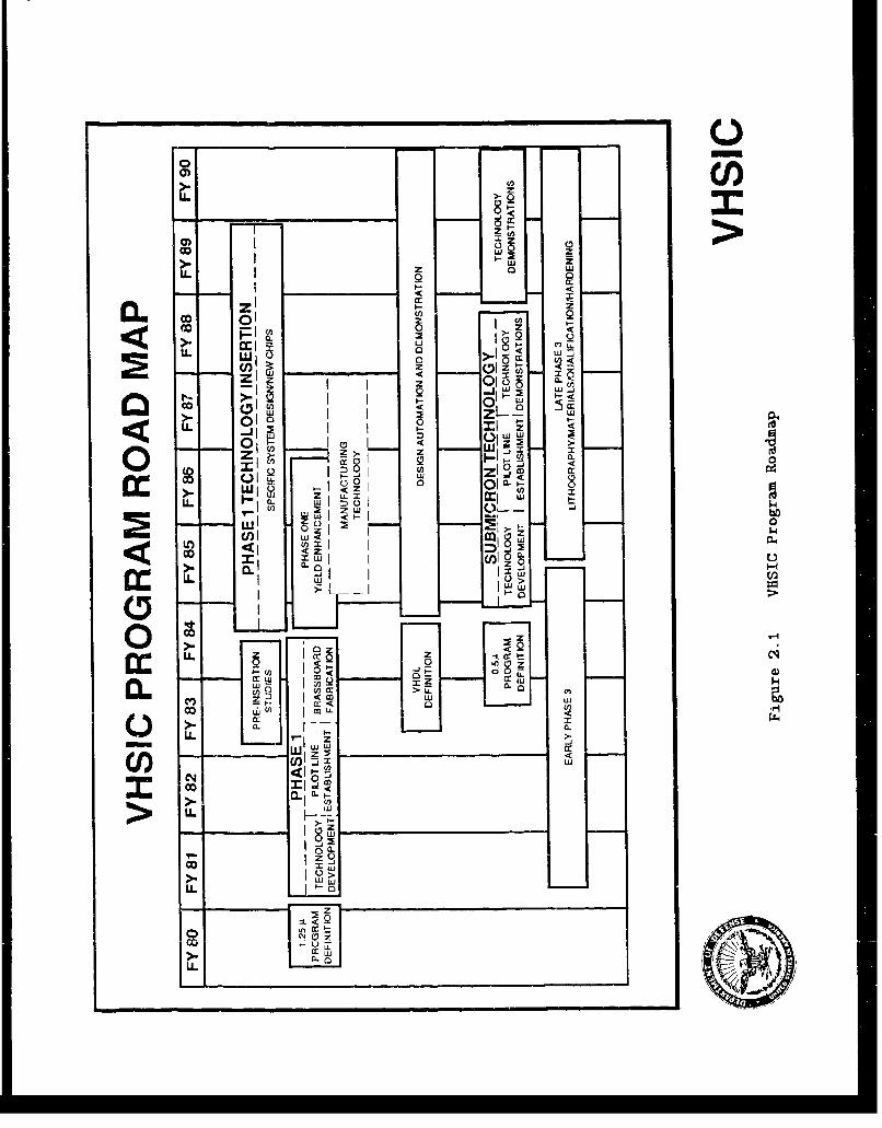
z
z 0
I-I
a: Qa-
cc~z.
CL co -ha:U
lo 0 0
01'-0IW S2 1S

.-4 Nl M~ to0 N- mf e) (N mA 'V 0D inin - 00 fn ;r (N .- 4 ( L n (n C14 LA
0; C.0 0 ' - 4 LA .L LA 4 C
>4i44
(h14 -4 0 C00 %D va C-4 0>4
OD '.0 ON N- N- a Ln
COD
LA)0 4 mv -4 U'. I--1-1 %D 0
C14 '.0 v CDC) 0 LA
C) cv 'N v~ 0 0 o-a r-'.0 N Ch( 0 0 N o>4 (N C44'. CD 0 ; in 01%
or C) ON Nf m N t- %Dn N C'
O co m .L
M CDC D m Lo o i
>4 (') C') C') -4C
Cý r- v -4
0) N, C ') ( '>L -OD *ý N>4 %D ýr I- to0 (D ' - D %D
NNC00 0 00 0
0~C C)) CD - 0L
00.
>4 0','. 0
o C) C
OD
%D CID
0
0) 4) 4J 4-)fro) ý r; F '-4 a) a) 0a ) 0 '4-4 .0 S4 4-) cl) a
U~C) 41) Q) z (a (d (a 0;j0 C) V) p
0n 1- 4 0s (n C'n (n)
P4 P-4 >4 E- n) P-4 P4 P4 P4 H 0
CHAPTER 2 / HISTORY, STRUCTURE, AND POLICIES
production equipment for dual-use and military devices was, and stil is, subject to EARcontrol.
One of the first actions of the VHSIC Program Office (VPO) to comply with theCongressional mandate was to draft a change to the ITAR that would bring VHSIC devicesunder ITAR control. The proposed entry, which was to be added to Category XI, wasforwarded to the Department of State by the Under Secretary of Defense for Policy (referredto hereafter as Policy) in December 1981. This entry read as follows:
"(d) Very High Speed Integrated Circuit (VHSIC) semi-conductor devices that are
specifically designed for military applications and which have a high-speedsignal and image processi.ng capability with an operational parameter greater
than 1011 gate-hertz/cm2 for an individual semiconductor device."
This entry was officially included in the revision of the ITAR which was published inDecember of 1984.
In 1984, there was a disagreement within the DoD over how to implement theCongressional mandate regarding the security controls for VHSIC. The technical siderepresented by the Under Secretary of Defense for Research and Engineering (R&E) generallyfavored minimum controls in order to foster technology transfer within the U.S. and with closeallies, while Policy recommended that the appropriate response to the Congressional mandatewas to classify the entire VHSIC program. While this action would ensure program security,R&E felt that it would create serious problems for the program managers in both the DoDand industry, as well as drive the program costs up sharply. For these reasons the VHSICProgram Office (VPO) considered it to be unacceptable. This classification issue thereforebecame an area of major disagreement within the OSD.
Efforts to reach agreement on the classification issue and other VHSIC securitymeasures continued within Defense without a consensus. As the discussions became protractedover an excessive period of time, Policy submitted its position to the Secretary of Defense forapproval. By this time, the Secretary of Defense had given primary responsibility for allexport control and technology transfer issues to Policy. The Secretary approved the Policyposition, and promulgated VHSIC security guidelines. While Policy set about to implementthe guidelines, R&E and some industry representatives advised the Secretary of the negativeimpact of these security guidelines. In an effort to make this more workable, the VPOprepared and submitted a VHSIC Classification Instruction (DODI 5210.75). Under thisInstruction, a VHSIC device would derive its classification from the system in which it wasused. The combination of this guideline coupled with industry pressure from the highest levelsfinally convinced Policy to agree to investigate and consider the use of industrial practices toprotect VHSIC technology.
While a VHSIC contractor panel was established to develop alternatives toclassification, Policy and R&E drafted a joint memorandum initiating a certification
45
CHAPTER 2 / HISTORY, STRUCTURE, AlD POLICIES
requirement for VIISIC-related contractors. The International Technology Transfer (IT 2)subpanel was directed to further evaluate VHSIC controls.
In an unrelated action, DOD Directive 5230.25, "Withholding of Unclassified TechnicalData From Public Disclosure", went into effect. This Dii'zctive is based on 10 USC Section140c, as added by P.L. 98-94, "Department of Defense Authorization Act, 1984", which allowsunclassified technical data under the control of a Defense element to be withheld from releaseto the public if it contains critical technology related to military or space applications.Certification procedures for contractors were included.
A second Directive, DODD 5230.24, "Distribution Statements on TechnicalDocuments", went into effect at approximately the same time. This Directive providedguidance regarding the marking of documents restricted from public release under DODD5230.25. The VHSIC Program Office directed that all VHSIC documents iestricted by DODD5230.25 would be marked with Distribution Statement X in order to ensure maximum possibleavailability to Defense contractors.
During the ensuing months, the VPO and its Policy counterparts in DefenseTechnology Security Administration (DTSA) attempted to reach agreement on a VHSICTechnology Security Instruction. DTSA had submitted the proposed alternative of theindustry panel for review by the Industrial Security Office within Defense. The industrydocument was rewritten by the Industrial Security Office into appropriate control language.The resulting Instruction, DODI 5230.26, "Very [igh Speed Integrated Circuit (VHSIC)Technology Security Program", imposed controls on unclassified information that were parallelto those required to protect classified information. A far more sophisticated certificationprocedure than was required by 5230.25 was also included. In spite of numerous negativecomments, this Instruction, dated March 17, 1986, was officially released in April 1986.
The VPO directed the VHSIC Program Managers to comply with this Instruction andtook the necessary action to have the requirements of this Instruction included as an interimrule in the DFAR. Nonetheless, few Defense contracts involving VHSIC were written ormodified in accordance with this Instruction.
With the Security Instruction in place, attention was turned to the development of aVIISIC export policy. The VPO prepared and submitted a series of release matricesemphasizing sharing with our allies for Policy consideration. In June of 1986, agreement wasreached and Policy drafted the export policy, based on the release matrix. DTSA forwardedthe first draft to the VPO in October 1986. A final coordinated VHSIC export policy wasissued on October 13, 1987.
A related security problem during the latter part of 1988 was the development of anexport policy for radiation hardened devices. The VPO was instrumental in quickly developinga policy on such devices that was acceptable to both industry and Government. This policydocument was promulgated by DTSA in April 1989.
During 1989 and 1990, the VPO worked with DTSA toward the cancellation of DODI5230.26, subject to modification of DODD 5230.25 to include specific reference to 'V HSICtechnology.
46

CHAPTER 2 / HISTORY, STRUCTURE, AND POLICIES
2.5.2 Additional Security Decisions
VHSIC was not just a program restricted to a few Defense contractors. It was the hopeand intent of the Congress and the VPO to recognize and encourage industry-wideparticipation. Products from every company that was able to design and produce devices thatmet VHSIC specifications were in fact tested, verified, and subsequently qualified for VHSICinsertion initiatives.
In the course of the program, it was periodically necessary for the VPO to providespecific policy on security regarding some element of the overall program. A summary of thekey determinations regarding VHSIC technology are listed below.
Date Subject or Action
February 1981 Briefing of all program participants on ITAR controls
January 23, 1984 Release from ITAR control of VHSIC HardwareDescription Language (VHDL) information
March 8, 1984 Release from IFAR control of VHSIC chip packaginginformation
August 5, 1985 Release from ITAR control of BIU data
October 15, 1985 Release from ITAR control of VHDL supportenvironment information
June 15, 1986 Release from ITAR control of VHSIC TISSS information
June 21, 1987 Definition of what constitutes a VHSIC device
December 8, 1987 Release from ITAR control of VHSIC chip packaginginformation
March 10, 1988 Public release of ADAS information
By the end of the program the VPO no longer considered it necessary or appropriateto single out "VHSIC" devices for special control. The diffusion of the technology throughoutthe industry and the availability of comparable technology in Europe and the western Pacifichad met the terms of the Congressional mandate for release from ITAR control.Consideration was given to generalizing the ITAR entry to read "electronic devices specifically
47
CHAPTER 2 / HISTORY, STRUCTURE, AND POLICIES
designed for military application" and deleting the gate-hertz/cm 2 performance parameterreferenced in the ITAR. The VPO supported the authorization of devices developed uaderVHSIC for use in commercial applications. Under this situation the result would be that a"VHSIC" device used commercially would be propeily identified as a "dual-use" device andthen be subject to the same EAR control as any other commercial VLSI device.
48
CIHAPTER 3 - DEVELOPMENT TASKS
3.1 D esign . . .. .. . . . . . . . . . . . . . . . . . . . . . .. . .. . . . . . . . . . .. . . . . . .. . .. 50
The Impact of VHSIC on Systern Level Design - Robert N. Rolfe ......... 51
3.1.1 Built-In Test/ Built-In Self Test (BITL 3IST) ....................... 563.1.2 Interoperability Standards . .................................. 603.1.3 VHISIC Jlardware Design Language (VHDL) ..................... 633,1,4 D esign Tools ............................................ 65
3.2 Test and Life Cycle Support .................................... 743.2.1 Test and Evaluation .......................................... 743.2.2 Test Technology ............................................. 793.2.3 Reliability and Q ualification ................................. 823.2.4 Maintenance Concepts for V1ISiC ............................ 86
3.3 C hip Fabrication .................... .......................... 88
The Impact of VHSIC on Fabricationi Technology - Charles S. Meyer ....... 88
3.3.1 1.25 Micron (Phase I and Yield Enhanccment) .................... S )7.3.2 0.5 M icfon (Phase 2) ..... . .................. ................ 993.3.3 Radiation Ilardenirng - J.ames J. McCarritv........................ 1043.3.4 "Improved Tools and Materials ................................ 1083.3.5 Packaging . .... ... ... ... ... .... ... ..... . .. .. . ... . ... ... 1 15
3A4 Description of VttSIC Chips .................................... 1203.41. Phase I ......................................... ....... 1203.4.2 Phase 2 ................................................ 134
49
CHAPTER 3
DEVELOPMENT TASKS
The goals for VI ISIC chip production were s..'. liz,'J by the values of their minimumfeature size --- 1.25 micron for Phase 1 and 0.5 miclun tor Phase 2. However, the completespecifications for VHSIC chips set limits for many other parameters such as functionalthroughput rate, radiation hardness, reliability, and temperature environment (see Chapter 2for Phase 1 and Phase 2 requirements). In addition, the program called for a variety ofimportant but less well defined requirements. Interoperability of VHSIC chips was neededbetween themselves and with other chips and electronic subsystems. Design methodologieswere desired which were more fully automated and which inMluded built-in (i.e. on-chip)testing. Packages for chips of these sizes, speed, and I/O count did not exist. New procedureswould have to be devised for testing and qualifying the chips for military use. If procurementfor production systems was expected, then second sources had to be developed.
Work in all of these areas of hardware and software technology became thedevelopment tasks that occupied the VHSIC contractors and the VHSIC Program Office forthe duration of the program.
This chapter describes in considerable detail the activities and the results of thedevelopment efforts down to the level of individual contracts. Further details are provided inthe references that are listed in each section. For readers not needing this level of detail, theintroductory paragraphs at the beginning of each numbered section provide a summary ordiscussion of the relevant issues.
3.1 Design
Although it was evident at the start of VIISIC that chip design and fabricationcapability were equally important to the final success of the program, it was not clear whichparticular design activitics should be supported by the Government. Obviously, the functionaldesign had to be included, but were there generic features critical for DoD applications thathad to be part of all designs? Were there design standards that should be implemented inorder to ensure manufacturability at reasonable cost, reliability, and adequate life cyclesupport? Were existing design tools capable of doing the job?
The direction of the design effort evolved during the course of the program. DuringPhase 1, stress was placed on design-for-test to ensure that fabricated chips worked reliablyand that they pc.formcd the functions for which they had been designed. In addition, designtool development was supported.
In the Phase 2 period, it was v,:alized that Government supported standardsdevelopment (rather than tool inprovemcnt) were activities that could have great industry-wide impact while at the same time meeting specific Dol) nceds. In the case of a hardwaredescription language, the VIISIC program not only created a standard (VHDL) but alsodemonstrated its use with a simulator and associated tools. Similarly, standards for the
50
CHAPTER 3 / DEVELOPMENT TASKS
interoperability of the Phase 2 chips were developed and used in their design. Greateremphasis was also placed on the interactions between the design of individual chipe And theoverall system specification and operation.
The following assessment of the impact of VHSIC on the procedures and tools forsystem level design has been included because it emphasizes the significant conceptual changesin approach that VHSIC promoted in its design automation developments.
The Impact of VHSIC on System Level Design
Robert M. RolfeInstitute for Defense Analys-s
Introduction
The advent of the VHSIC program focused attention on the concept of "asystem on a chip" and thereby brought to the forefront the following problems thatuntil then had not been adequately addressed by chip designers,
"o Making full use of the tremendous number of transistors (or gates)available to the designer in a VHSIC microcircuit can lead to lengthydesign time and very high design cost.
"o The high cost of large, complex, application specific chips makes anyincremental change to older systems expensive and therefore discouragingunless significant needed system capabilities are added.
"o Quality assurance and testing of the chip are no longer independent ofthe sysLem integration process but must now involve system levelspecifications.
"o System design requirements for software, maintenance, and life cyclereliability must also now be considered at the chip level.
These problems argue that the design of the chip architecture mustincorporate the necessary test strategy to remove latent manufacturing defects aswell as a test strategy for design verification to remove latent design defects. Onecan ask how one provides a design that is capable of identifying manufacturingdefects in a structure containing millions of interconnects and active elementsthrough an interface with only a few hundred electrical signal ports (namely, thechip periphery pads).
The VHSIC Hardware Description Language (VHDI_), described in detailin Section 3.1.3, is the hub arouncl which many specific tools have been created toaddress these problems. It supports model-based specifications which can be used
for simulation and other analyses. 51

CHAPTER 3 / DEVELOPMENT TASKS
A comprehensive implementation of the IC design process must consider ahost of specific issues if it is to be effective in meeting functional and physicalrequirements that will surely get even more complex and more difficult in the
future. Several of the most important are discussed below.
Design Methodology
Hardware/Software Trade-Off Analyses
One of the first issues that must be resolved in a complex system design isthe allocation of various system functions between hardware and software.
Premature binding of the system architecture to a specific solution may decreasesystem performance, adaptability, and maintainability. Incorrect allocation of
system functions to hardware or software will delay system development and agethe design solution unnecessarily. Under the VIISIC program several softwaretools were developed to support analyses of proposed allocations. ADAS (theArchitectural Design and Assessment System) and the JRS Automated VHDL/Microcode Compiler, described in Section 3.1.4 address these issues. ADASprovides a capability not only to analyze but also to refine the system architecturewhile the JRS tool provides a path to reusable macrocells of a silicon compilerleading to actual layout of the chip. The latter capabilities can greatly increasedesign efficiency and quality since the silicon compiler macrocells will have been
prechecked for functional accuracy.
Information Reuse
The VHSIC software products enable reuse of engineering information reuseduring and after the process of designing the system. These products includeVHDL and its descriptions of standard component models and test program sets.
Engineering information reuse in a controlled process enhances concurrency of thesystem design process which shortens the dcsign time while providing higherquality. VHSIC has also developed a specification framework for engineering
information systems (EIS) to support access to shared information for tools andusers. EIS is discussed below.
Product and Process Qualification
Using qualification or acceptance tests of a product chip after themanuf,3cturing process to provide quality assurance ignores the tremendous impactof early engineering design decisions on the product quality and maintainability thatis ultimately achievable. Qualification of the design as well as the manufacturingprocess reduces qualification costs when amriortized over a quantity of products andproduct types produced through the qualified processes and, at the same time, itincreases the product quality. The VtlSIC program focused on development and
52
CHAPTER 3 / DEVELOPMENT TASKS
manufacturing process qualification with the Qualified Manufacturing Lines (QML)concept (Section 3.2.3). This concept has the potential for not only reducing "redtape" but also for ultimately improving product quality by not constraining designand manufactuiing process solutions. It shifts the focus to pre-assured design andmanufacturing qua'ity versus "tested-in" quality.
Built-in Test and Maintenance
System test and maintenance have become one of the most important issueswhen designing highly complex systems comprised of highly complex chips. Incontrast to other issues where the correct design methodology allows manydifferent possible implementations, test and maintenance require standardizationby specification at the hardware interface level to permit chips designed by differentorganizations and at different times to be used together in systems. The VHSICprogram has developed a number of new system architectural features to facilitatethe integration of complex chips into systems and to provide for their test andmaintenance. (For details see Sections 3.1.1)
The standard for a powerful, general purpose backplane bus, the PI bus, hasbeen developed by VHSIC for data communications across local backplanes. Thisstandard is being used for the most recent tactical aircraft avionics programs.
Built-in test technology was mandated as part of the original VHSICrequirements, and the contractors have developed a number of enhanced techniquesLu accomplish it. Examples include level sensitive scan design (LSSD) and otherscan design techniques to fully automate detail tests of the chip structure used inmanufacturing and maintenance.
The architecture and specification for a test and maintenance (TM) bus weredeveloped by VHSIC to support built-in test (BIT) for electronic subsystems. TheBIT architecture integrates the built-in element test and maintenance (ETM) busof a single VHSIC microcircuit with the subsystem TM bus. VHSIC-basedelectronic subsystems which use these integrated test buses can be expected to beself-diagnosing for most of the anticipated fault modes. This self-diagnosisincludes identification to the faulty component even in a two level maintenancestrategy.
Computer Aided Test
The VHSIC program has developed an approach to a methodology fortesting VHSIC class microcircuits. The essential element of this approach is todevelop and validate a language which allows the capture of the product and testspecifications which, in turn, are linked to a set of standard test methods (e.g.MIL-STD-883) for VHSIC class microcircuits. By separating product and testspecifications from the implementation of test programs, VHSIC developed teststandards that cnable innovative computer aided test tools and extensive reuse ofproduct descriptions over the product life cycle.
53
CHAPTER 3 / DEVELOPMENT TASKS
This capability was demonstrated in the VHSIC Tester Independent SupportSoftware System (TISSS) discussed in Section 3.2.2. An extension to the TISSS,the Line Replaceable Module (LRM), is currently being developed for the AdvancedTactical Fighter (ATF) and the Joint Integrated Avionics Working Group (JIAWG).The JIAWG goal is to use simulatable product and test specifications for commonmodules across DoD weapons platforms.
Engineering Information Management
Any design as complex as a VHSIC based microcircuit system requires largedesign teams with concurrent access to product description information over thedevelopment cycle. The VHSIC Engineering Information System (EIS) hasaddressed this need by defining a generic set of standards for computer aidedengineering and design environments (Section 3.1.4). The basic EIS provides lifecycle support of any well described product and has demonstrated this for designand layout information modeling.
Standards and Practices
The VHSIC program has had a strong impact on commercial electricalproduct standards activities within the IEEE and the Electronics IndustryAssociation (EIA). VHSIC provided strawman standards for the DesignAutomation Standards Subcommittee of the IEEE including IEEE 1076 VHDL andIFEE WAVES (Waveform and Vector Exchange Specification). The VHSIC Phase2 test and measurement bus (TM bus) was provided to the IEEE test busstandards committee. The EIA has drafted standards to use the IEEE VHDL forthe specification of digital products and set out to develop guidelines for use ofVHDL for the specification of standard industrial components. If approved, thisguideline will become EIA 567.
The IEEE 1076 VHDL standard has been accepted for use in the commercialCAD industry even faster than in DoD (see the contributed paper in Section 7.2).Major commercial system developers have adopted it, and the marketplace now
has a growing base of available computer aided engineering vendors supplying IEEE1076 VHDL products.
The VHSIC program advanced the concept of virtual test of products basedon simulatable specifications and designs. 'This fact not only shortens designintervals, but effectively removes a large category of latent design defects beforeprototype or breadboard fabrication. The feasibility shown by the VHDL simulatorbuilt as part of the VHDL contract with Intermetrics encouraged the CAE industryto develop system level and design phase simulators. Today, many commercialsimulators are available for the VHSIC developed VHDL. Some of these simulatorswill even allow detailed VHDL descriptions of complete processing systems to hostsoftware development before the physical prototype is available. This capabilityenables design teams to practice concurrent engineering for software on customhardware platforms.
54
CHAPTER 3 / DEVELOPMENT TASKS
The following are some specific activities in standards and practices :,hathave taken place both in industry and in the Department of Defense.
o The Design Automation Standards Subcommittee of the IEEE hasrecently indicated it will develop a product and test specification languagestandard with strawman input initially derived from the VHSIC TISSS.
Use of this strawman language already has demonstrated largeengineering productivity improvements in the development of VHSICqualification test programs.
oThe Computer Aided Acquisition and Lo~.i~tics System (CALS)
specification references the IEEE 1076 VHDL for digital electronicproducts behavior description in MIL--STD--1840. IEEE 1076 VHDL isthe only standard language for hardware behavior functionality. CALSdelivery of VHDL electronic product descriptions that emulate productbehavior and interface specifications will be exploited for many decades.
o The VHSIC program has developed a standard data item description(DID) by which procurement contracts in the DoD can define theelectronic media delivery of hardware descriptions. MIL--STD--454 was
extended to include VHDL and TISSS descriptions for microcircuits thatmust conform to DoD Requirement 64.
o The VHSIC TISSS product and test specification model is to be extendedby the ATF program to support the full scale development (FSD)
acquisition statement of work (SOW) by specifying requirements fordelivery of simulatable specifications. The USAF Modular AvioniesSupport Architecture (MASA) plans to adopt tailored versions of the
JIAWG simulatable specification requirements.
o Specifications of digital subsystems for reprocurement should be greatlyimproved by the VHSIC developed product and test specification and
hardware description standards. Reprocurement is a critical issue in theDoD for long lived, routinely operated, space systems and complexweapons platforms.
oThe ASCM (Advanced Spaceborne Computer Module) follow--on to the
GVSC (Generic VHSIC Spaceborne Computer) is to be a standardmodule, consisting of many subassemblies, for spaceborne processing.
The GVSC program beta tested the VHSIC TISSS standards for productand test specification standards.
Long Term Systems Design Issues
Thp VHSIC program has identified opporttlniti• to improve design of
systems in the future, in particular, the EIS has identified the need to develop
55
CHAPTER 3 / DEVELOPMENT TASKS
better information modeling concepts, methods, and tools. Although theintegration of product data across the organization has been addressed for wellcooperating engineering information systems, weakly coupled systems underautonomous control still pose an important challenge; most of our existingoperational and maintenance support systems operate in this manner.
The VHSIC program has made great strides in built-in test (BIT) for digitalmicrocircuits and tightly coupled subsystems, yet much effort must be made tofully integrate test architecture across systems. Accurate BIT remains a problembecause VHSIC BIT solves the problem for only a small spectrum of electronic andmechanical systems.
Powerful BIT architectures create the need for significantly advancedautomatic test pattern generation (ATPG) tools for manufacturing and productsupport. The ATPG tools have hardly kept pace with system design tool progress.VHSIC has attempted to address this with standard test architectures, testinterfaces, and product description languages. Yet, much work remains indeveloping product description models that allow system designers to describe testarchitecture for the full spectrum of electronic and mechanical technologies used ina modern weapon system.
3.1.1 Built-In Test/ Built-In Self Test (BIT/BIST)
Complex digital systems consist of a hierarchy of chips, cards, and racks. At each level,tests must be performed to ensure that components work reliably in accordance with theirdesign specifications and are free of any logic errors and timing problems. In addition to testsof this structural organization, tests must also be performed at different times during the lifecycle of the various components: after manufacturing, at system start-up, and during on-lineor off-line operation.
In order to meet these diverse testing requirements, special hardware must beincorporated into chip and card designs to render the components testable down to levels atwhich faults can be isolated (Built-In Test). For a chip, this is the gate level. The techniquesfor producing such tcstalA:c ;2csig.uz.3 requir- q conp-'-hensive implementation methodologyusually referred to as design-for-test (DFT). While Built-In Test requires external test vectors,components with Built-In Self Test capability can generate their own test vectors and reporttheir status to the outside world. Such capability ;s important for quick response, on-lineoperation testing, or to decide whether redundant elements are needed to be activated in faulttolerant designs.
During Phase 1, design techniques were developed, documented, and demonstratedwhich provided increased reliability and testability of chip performance through the inclusionof on-chip tcsting and fault tolerant designs. The details are to be fuund i4 Refeleices 2.11-2.15. Phase 2 extended this work to encompass standards for chip-to-chip and card-to-cardcommunication (Section 3.1.2). TRW used BIST to improve fabrication yield on its
56
CHAPTER 3 / DEVELOPMENT TASKS
"superchip" to acceptal le levels by connecting enough working macrocells together to form afunctional chip. The Phase 2 work is described below.
Honeywell
The Honeywell approach to BIT/BIST was to include presettable sequential "flip-flops"(FFs) in all chip designs in such a way that all combinational logic and sequential elementportions of the circuit would be testable. Loading a value to one FF causes the propagationof that value to another FF where the value can be captured and scanned out. This techniqueis very similar to IBM's level sensitive scan design (LSSD) technique and became the basis ofHoneywell's standard design-for-test procedure.
To ensure defect free components and boards, Honeywell included both internal andboundary scan in its Phase 2 chips. With internal scan, all of the normal functional flip-flopswithin the design are replaced with scannable registers, i.e. registers whose setting can besensed. Serial access to the internal registers, combined with computer generated test patterns,gave greater than 98% coverage of single stuck-at faults within the components. To implementboundary scan, scannable flip-flops were placed at each I/O pin to allow direct serial accessto the chip I/O. This boundary scan approach, visible only during board test, providedthorough testing of interchip connections at the board level.
To meet the need for high coverage self-test, Honcywell implemented two approachesto pseudo-random self-test. The primary approach was to replace all registers in the designwith registers known as Built-In Logic Block Observers (BILBOs) which support normalfunctional mode, test reset, test serial shift, parallel pseudo-random test pattern generation,and parallel signature analysis. By using BILBO registers throughout the design, parallel testpatterns can be applied to the chip at full chip speed. In addition to this parallel approach,serially loaded pseudo-random test patterns are also supported to allow a cost/coveragecomparison of these two approaches.
Honeywell chips included the element test and maintenance (ETM) bus (the chip leveltest bus) as the standard interface to the BIT circuitry to allow either pseudo-random patterngeneration on the chip or deterministic patterns to be scanned in. Pseudo-random techniquesallow high fault coverage testing of the internal circuitry of an IC.
A hierarchical maintenance system was designed with two levels of test interface, a chiplevel interface (ETM-bus) and a backplane or board level test maintenance interface (TM-Bus). Individual Honeywell chips include an ETM interface. They can be connected to atHoneywell Test Interface Unit (TIU) for communication of chip test information to a systemtest controller. The TiU device was fabricated, packaged, tested, and documented in VHDL.An applications board will be developed as a VHSIC add-on task. The TIUs connected to theTM-Bus can provide the system test controller with diagnostic information.
57

C-t"TIER 3 / I)EVELOPMENT TASKS
113M
The IBM design methodology for built-in test was to use level sensitive scan design(LSSD) coupled to the standard ETM bus interface. LSSD ensures that all sequentialelements can be set to arbitrary values from an external interface. This allows the complexityof the test generation to be reduced to that for a combinational circuit. The LSSD latches canbe set to known valueF with external test vectors or by using internal linear feedback shiftregisters to generate pseudo-random patterns for built-in self-test. Pseudo-random patternsgenerated on chip can transfer data to the ILSSD latches at a much higher rate than patternsexternally scanned in. BIST stuck-at fault coverage was 59.4% for the AC chip, 90% for theCSR chip, 54.6% for the SP chip, and 78% for the V1I3LJ chip. For IBM, BIST can test onlythat logic bounded on both sides by an LSSD latch so that the logic between the LSSD latchesand the I/O pins renlains untested. This is tested by a "boundary scan" procedure thatsupplements the BIST. These two test procedures used together produced a combined faultcoverage of greater than 97% for all chip types.
The system level BISTl design used a hierarchical test bus architecture in which all chipscontain ETM Bus interfaces. These chips are connected to a diagnostic maintenance device(DXMl)) that contains the interface to the module level TI'M Bus. The DXMD was notftbricated for the VHSIC Phase 2 program. The TM-Bus can connect to IBM's "availabilitymanagement system" for system level diagnostics and testing.
I'RW
.T'RW's BIST approach was to partition a superchip into three sections: logicmacrocclls, interconnections between logic macrocells, and RAM arrays. The 131ST systemfirst tests the logic macrocelis, then uses working nlacrocells to test interconnections betweenmacrocells, and finally uses the working logic macrocells and interconnections to test thememory arrays. A serial test bus, the Logic Macrocell Test Bus (LMT Bus), providescommunication between the central test processor and the local test hardware resident in themacrocells and supports testing at full chip speed.
Figure 3.1 illustrates the BIST system. The superchip 131ST system minimizes thehardware located in the test node of macrocells tvider test and the size of the test bus. Testpattern generation and timing control hardware are located in the central test controller. T'he1,MI' Bus consists of four multiple-drop lines with pipelined repeaters. This test bus supportsat-speed logic macrocell, interconnect, and memory test with a simple protocol, thusminimizing bus interface hardware in the macrocell test node, the Logic Macrocell Test Slave(LM'IS). All bus transact ions are controlled by the Logic Macroccll Test Master (LM'TM) inthe central test controller.
Thie LMT master provides the capability to generate the LMT Bus packets necessaryto control LMT slaves for macrocell verification, configuration, and maintenance. A varietyof co,'trol and data streanlis, inccludihg psA.-,ra-dt'•i11 |,tte.lu., walking I's atid O'•, N.nd solid
58
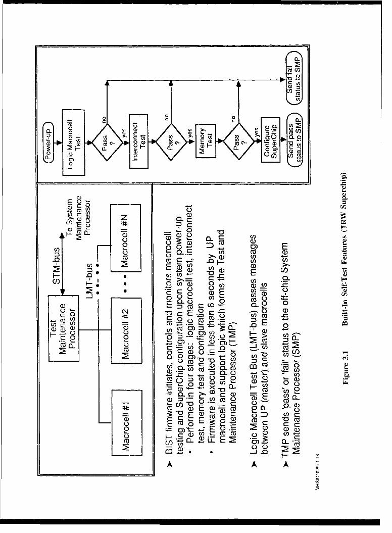
0-
-0
ci:
0 c 0
CL ) (f)
Q)0 Q) 1cn'
-9~~ cl C~.~
i.-- Q). I)_
00
EE
>,D C) a)v U)_U) Z 0
r-o 0 fQ,0a
0.-I VC ~
L))0, 0
czj
.- I cI
CHAPTER 3 / DEVELOPMENT TASKS
O's and l's, can be generated with minimal external control. The LMT master can controlmany other test busses including the ETM Bus and commercial scan registers.
The LMT slave responds to LMT Bus commands in order to exercise real-time controlover macrocell operation and perform at-speed compression of test results into an accessiblesignature. It also provides half rate and quarter rate clocks for the macrocell. Each logicmacrocell contains an LMT slave.
3.1.2 Interoperability Standards
Although several projects used Phase 1 chips from different vendors on the same board,it was realized that the interoperability between new VHSIC chips (both 1.25 and 0.5 micron)from different vendors would be greatly enhanced if standards were established to specify theirelectrical, data path, and test bus interfaces.
Accordingly, the VHSIC Phase 2 Statement of Work, issued in 1984, stated thefollowing requirements for interoperability:
"INTEROPERABILITY STANDARDS:
lnter/lace/Interoperabilityv Standards shall be established by agreement among allVHSIC Phase 2 Submicron contractors and the Government COTRs to assure thatall chips deLveloped under the VIISIC Phase 2 Submicron Program areinteroperable, both electricall/) and physically. Standard ivoltage level(s) shallbe established and utilized for all chips and input/outpat levels shall be equivalentfor all chip inter faces, whether contained in a single or multi-chip package. AVHSIC half-micron Bus Interfaice Unit (BIU) chip shall be developed to facilitatemodule interoperability with a Standard Interconnect System Bus. The BIU andany other VHSIC chips developed under this Phase 2 VHSIC SubmoicronProgram shall interface directly to a Standard System Maintenance Bus to bedefined by agreement among all the VHSIC Phase 2 Submicron contractors andthe Government COTRs. All these Standards shall be documented and delivered."
In accordance with this paragraph, a tri-Service Interoperability Committee negotiatedfour standards with the Phase 2 contractors (Reference 3.1). These were (1) electricalinterface standards, (2) the parallel interface bus (PI-Bus), (3) the test and maintenance bus(TM-Bus), and (4) the element test and maintenance bus (ETM-Bus). The standards exist ascopyrighted documents to prevent the propagation or publication of unauthorized changes, butthey may be copied without modification. They are "open" standards, and may be used byanyone. The following is a description of each and its current status.
60
CHAPTER 3/ DEVELOPMENT TASKS
Electrical Interface Specification (Version 2.4. January 1988)
This standard provides interoperability between all Phase 2 chips, new Phase 1 chips,and standard TTL-I/O chips. Its purpose is to ensure the operation of VHSIC Phase 2 ICsfrom various vendors on the same board.
To permit the use of the Phase 1 chips and Phase 2 chips on the same board, newPhase 1 chips should comply with the Electrical Interface Specification, except that they willutilize a maximum 25 MHz for the SYSCLK signal frequency, and the DFNCLK signal willbe operated at 1/4 of the SYSCLK frequency. Since both Phase 1 and Phase 2 chips operateat a maximum 25 MHz chip I/O at the package edge, this will provide direct interfacing.Redesign of original Phase 1 chips are expected to meet this specification also. It will ensurethat chips which use the name "VHSIC" will enhance rather than detract from the "-ilities" offuture DoD systems.
For existing printed circuit boards, the maximum I/O rate presently supported is 25MHz. This limit is imposed by the physics of the board level interconnects. In the future, ifimpedance matched lines are used, higher I/O rates will be feasible. Both Honeywell and IBMhave demonstrated that 50 MHz communications are achievable between ICs with impedancecontrolled lines on a multichip carrier. In addition, the Laser Pantography effort at LawrenceLivermore National Laboratory has constructed "Silicon PC Boards" with propagationvelocities of 23 cm/ns as part of its VHSIC Phase 3 effort (Section 3.3.4).
Parallel Interface Bus (Version 2.2, March 15 1988)
The PI-Bus standard specifies the backplane parallel interconnection betweenVHSIC-based subsystem boards. Unlike microcomputer busses such as the VME, MultiBus,or FutureBus, the PI-Bus has no separate set of lines for addresses. This bus is meant to bea communications medium for systems to exchange messages or buffers of information, andnot for CPUs to retrieve individual words from a memory. The bus provides a choice of 16-or 32-bit wide data paths, in either an "error detection" or a "single error correct, double errordetect (SECDED) mode". All three VHSIC Phase 2 contractors have chosen to implementa 16-bit, error detection version of the BIU as a PI-Bus interface for their demonstrationmodules. IBM has over 1200 fully tested chips available. Honeywell has at least one fullyfunctional part, and has packaged parts undergoing life testing, while TRW/Motorola hasabout 2700 functional BIUs which passed wafer probe. The bipolar drivers for the backplane-irc now available on the commercial market from Signetics. The PI-Bus is a standardinterface on the Air Force Common Signal Processor (CSP) and called out in SDI technologyprograms such as the Advanced Spaceborne Computer Module (ASCM). It has been chosenby the .oint Integrated Avionics Working Group (JIAWG) as the backplane control bus for,hr- \TA/ATF/ATI-l common avionics package. ,They will use a 16 bit error correcting versioni (f) ,, 111; buls configuration, along with a dual TM-Bus, a MIL-STD-1553B serial bus, and a
')ch petd D)ata Bus. The Air Forcb ATF and the Army ATI-H (or LHX) a'we each in the
61
CiIIAPTLR 3 / DEVELOPMENT I ASKS
DeonOnstration/Validation phase with two competing contractor teams. By the ATF/ATA/LI IXCommonality Memorandum of Agreement between the Services, the Navy is committed to ap 3I program to use the JIAWG specifications, and all three Services are committed to usingthe JIAWG avionics specifications/standards in deliveries after 1997. It also should be notedthat the SAE-9 HIINT committee, which was tasked to define a new parallel backplane bus,has selected the PI-Bus as the candidate for a new standard.
Test and Maintenance Bus (Version 3.0,.November 1987.
The TM-Bus provides a serial backplane interconnection for the same 32 module setserviced by the PI-Bus by using four interconnect lines: Clock, Master Data, Control, andSlave Data. The TM-Bus is used by the Phase 2 VIISIC contractors on their demonstrationbrassboards. In addition, it is being quoted as the maintenance interface for several VHSICcontractors insertion efforts, and will be used by the ATA/ATF/ATH as explained in theIII-Bus section. The TM-Bus is being incorporated into draft standard IEEE 1149.5.
Element Test and Maintenance Bus (Version 3.0, November 1987)
The ETM-Bus standard provides the electrical and protocol definitions for asynchronous serial bus. This standard allows the designer to use chips from various VIISICmanufacturers on the same board and connect them to a common maintenance controller,which in turn receives its control and instructions via a backplane TM-Bus. A singlecontroller can thus be used to test a board in both field and depot maintenance operations.
Because of interaction between the VHSIC ETM Bus group and the Joint Test Action(JTAG) working group, the proposed IEEE P1149.1 standard IC test bus proposed by JTAGcamne to be quite similar to the VIISIC ETM Bus. Honeywell has even designed a buscontroller chip which will work with either bus although some differences remain between thetwo busses. The likelihood of wide acceptance of the P1149.1 bus in the commercial marketmakes it reasonable to expect it to supersede the ETM-Bus, even for military systems.
Maintenance of the VIISIC Bus Standards
Soon after the VI ISIC bus standards were first proposed, a group at the Naval OceanSystems Center encoded the PI- and lM-BLIsses in SIMSCRIPT and simulated them fordifferent message types and load conditions. Several inconsistencies in the protocols, as wellas ambiguities in the specification documents were discovered and corrected.
In 1988, whe,' VIII)L had become an IEEE standard, the VIISiC InteropcrabilityCommittee decided that the bus standards shoutld be rewritten as VI tI)L descriptions to allowtcstI of the standards to be made in the widtely availa'ble VI1) 1 environ ment In addition, itwould also allow a designer to actually use a simulation model for a VlISIC bus with the
62
CHAPTER 3 / DEVELOPMENT TASKS
simulation of his system in order to evaluate which busses (16-bit, 32-bit, etc.) best fit thedesign requirements.
A team at the Science Applications International Corporation was contracted to writethe bus specifications and test environment for both the PI- and TM-Busses in VHDL. Theproject was successfully completed in May 1990, and the entire system was demonstrated at theNaval Research Laboratory.
Copies of the VHDL PI- and TM-Bus specifications are available for computerdownloading from the Naval Research Laboratory, Code 5305. A modified version that agreeswith the Joint Integrated Avionics Working Group backplane specifications is expected to beavailable in the future.
3.1.3 VHSIC Hardware Design Language (VHDL)
Like many programs, the VHSIC Hardware Description Language (VHDL) was bornout of necessity. By 1978, at the inception of the VHSIC program, DoD was alreadyexperiencing an unmanageable situation with parts obsolescence. Early VHSIC studiesforecast that by 1990 about 80% of non-memory components in DoD systems would beApplication Specific Integrated Circuits (ASICs). Additionally, the average lifetime of a semi-conductor fabrication process was projected to be shortened to about two years. With theaverage system development cycle for DoD systems being 7-10 years, DoD was assured ofparts obsolescence before a system was fielded.
The use of a Hardware Description Language (HDL) was viewed as the solution to theproblem. By capturing the function of the device, as well as its hierarchical structure, atechnology independent documentation would be created that could be used as a procurementspecification to build new devices that performed the same function as the old one, but wouldbe constructed in the prevailing technology. In addition, the HDL would produce a simulationmodel of the device that could be used to simulate at board, subsystem, and system levels.'[hus for the first time l)oD could also have the benefit of accurately knowing theperformance of systems before construction.
While the obvious solution to the problem was the use of an HDL, in late 1979 and1980I there were no commercial HDLs available. l-IDLs were in use in universities and customcomptuter aided design environments within large corporations.
I)ol) VIISIC program personnel believed that an industry standard hardwaretkd,,ription language (Ill)L) was needed. In late 1979 through 1980, surveys of HDLtclihnology were made. The conclusion was that while there were many I-IDUs in existence,:!]Iýwrce ither too limited in scope or proprietary. Thus, in the summer of 1981, the VIISIC,,h1ic ,ponsorcd a workshop at Woods H lole, MA, gathering together language experts from1)0t,1lVi, ,icaidcmii, and government, to define the requirements for a hardware descriptionI;twi,:ii,', . Oli, wmkdhiop pro(luce• (locumcntlation that was used to generate a specification
Ill .uly I 98;' ;1 Contract wa.s awardeI(I to Intermetrics, tearmed with 113M and Texas1(. ) , Ir• ve•1v•p "I VIISI C hardwaire description language, simulator, and other
0.1,
CHAPTER 3 / DEVELOPMEN1 TASKS
associated tools (Reference 3.2). The resulting VIIDL version 7.2 was released in August1985.
In December 1985, VHDL 7.2 was submitted to the IEEE as a candidate hardwaredescription language standard. As a result, the IEEE created the VHtDL Analysis andStandardization Group to standardize the language. The VHtSIC Hardware DescriptionLanguage (VHDL) became IEEE Standard 1076 in December 1987 and ANSI/IEEE 1076 inOctober 1988.
Since that time, the VI-IDL technology has been successfully transitioned to industry,academia, and government. About 50 Computer Aided Engineering tool suppliers haveVHIDL oriented products either on the market or in development. The IEEE and ElectionicIndustries Association are developing additional standards and practices based on VHDL. itis in production use within many companies and it is currently cstimated that there areupwards of 1000 sites with VHDL capability.
In 1988, a VHDL Users Group was established first as an independent organizationand, since June 1989, as a Technical Users Group under the IEHE Computer Society. Therearn currently about 800 members of the users group. More than 50 universities have VHDLactivities rangisig from research in areas such as design synthesis and formal verification, tousing the language as a teaching aid in the design classes at junior level and above.
The Government has a wide variety of VHDL activities underway. VHDL was addedas required documentation under MIL STD 454 Requirement 64 as of September 1988. Al)ata Item Description to cover VHtDL documentation under contract, was developed by a tri-Scr% ice working group and became effective as DI-EGDS-80811 in May 1989. In cooperationwith industry, t: government has agreed to establish validation procedures and certificationprocesses for VFI-DL models. This capability is expected to be on line by October 1990.Additionally, work is currently underway to place VHDL. documentation requirements intoMIL STD 1840 and usage guidelines into NiIL Handbook 59 under the Computer AidedAcquisition and Logistics System (CALS) and to certify VIIDL as a Federal InformationProcessing Standard (FIPS) in conjunction with the National Institute of Standards andTechnology. The FIS requirement covers svstems through components, and extends therecquiremnent to all government agencies.
Internationally, significant efforts with VItI)Dt are u dcrv'ay in many countries,including Canada, England, France, Germany, Israel, Italy, Japan, Korea, and Sweden.
VIHIDL Lapgpa4ge Definition and Devclopmcnt
The dcfinition and developmcnt of VIIDL was the cornerstone of the VHSIC designautomation program, and was carried out under ai -act with Intermetrics, Inc.Implementation of software started in August 1984, and .. aued into 1988. The softwaret10ol sOt developCd inIcLI(led an analyzer, design library rnanagcr, reverse analyzer, andsimulator. In September 1987, at VIIDL language version for IFEFE standardization wasreleased, and, on I)eccnibc 10, 1987, the VIII)L was approved as IEEE Standard 1076.Adoption of VHI)L as an ItLEE standard was a major VI ISIC milestone, a step that ensures
64
CHAPTER 3 / DEVELOPMENT 'rASKS
thai VHSIC designs documented in the VHIDL will be readily transportable throughout thecommercial and military IC design communities. The VHDL IEEE 1076 software (analyzer,dc.IiLgn library manager, and fully interactive simulator) was delivered during 1988. Softwareis now production quality and resident on VAX/VMS and Berkeley UNIX on Sunworkstations. An EDIF interface was added in 1990.
A VHDL newsletter is available from Intermetrics which regularly publishesinformation related to VHDL.
VYIDL Independent Validation and Verification (IV&V)
The purpose of the IV&V effort was to test the VHDL software in actual use in thefield. The primary contract for this effort was awarded to the United TechnologiesMicroelectronics Center in August 1985. The work was divided into two parts. The contractorperformed an initial test of the VHDL software and then acted as a focal point for secondarytesting at "beta" sites. User comments from the beta test sites were incorporated into theIEEE 1076 version of the VhDL software. The contract was completed during 1988 and thispart of the program concluded successfully with VIIDL as a production tool.
Joint U.S./Canadian Rehost
Under the Joint U.S./Canadian program started in July 1987, the VIIDL tools wereadapted for use with high performance workstations. The U.S. provided the VHDL software,graphics interface, EDIF interface, validation tests, and technical consultation. The Canadiancontractor, Bell Northern Research (BNR), installed the VHDL software on various high-end workstations and integrated some of its own design tools into that VHDL environment.The tools were ported to ,ui APOLLO 4500 series platform and beta testing began in March1990 for commercial release in June 1990. A DEC PMAX port was completed in May 1990,and beta testing began in .luly. Significant impiovements to simulation efficiency were madeby BNR. By using a different algorithm for event que management, a simulation speedimprovement of 50 to 100% was achieved from the version 1.5 to version 2.1 of theIntermctrics tool set. I3NR has also developed an EMACS based editor for VHDL that isavailable through the Canadian University Network. Additionally, work is progressing tointegiate the VIHDI.. system into the Cadence framework. The joint proj,,ram is due to becompleted in 1992.
3.1.4 D)esign Tools
At the very conception of the VI ISIC program it was realized that in order to designchips of the required functional complexity. it would bh neccssary to employ computer aideddesign to a much greater extent than was current at the time. Furtlh'rmore, the high cost and
(5
CHIAPIER 3 / DEVELOPMEINT TASKS
lengthy turn-around time of chip fabrication made it almost a necessity that designs be correctthe first time.
In 1980, chip design was a compartmtentalized process performed by separateindividuals (or groups) using mostly manual methods. An integrated design methodology wasneeded which would utilize a set of automated design tools that would work together. At thattime, among the six Phase 1 contractors, only IBM possessed an adequate CAD capability.
Dluring Phase 1, the contractors were tasked to develop integrated CAD systems withwhich to design VIISIC chips. ttowever, as described in Section 2.2.7, this approach was not.practical and subsequently, much more focused goals for the VHSIC design tools programwcre formulated. They were three-fold:
"o to provide advanced design tools to support the designer using the VHDL,"o to develop system level advanced design tools, and"o to develop a comprehensive framework in which the design tools and design data
could operate.
VI !I)L Insertion Tools
Workstations/Interfaces: The purpose of this effort was to develop terminals withinterfaces which assist the designer using VIII)L.
Gould (via subcontractor Vista Technologies) developed at prototype genericworkstation intcrtace for VIII)L using a SUN 3 workstation, which automated thegeneration of VIII)L co,,uc .iod checked for internal consistency. The work wascompleted successfully, and tie final software was delivered in December 1987 to theArmy at Ft. Mo1nmouth an~d the Navy at thc Naval Research Laboratory for evaluation.The new VIII)L workh'--nch allows a designer to input schematic diagrams and haveVI!I)L structural descriptions compiled in real time. If functional descriptions aredesired., the system provides "hand holding" by means of a syntax directed editor, Theuser can create VII )L code cvcn with limited knowledge of the language. This systemis a designer's entry into VI II)L. Thc technology embodied in this program is beingcommerciali,,cd by Vista T"cchnologies, and Vista is under subcontract to Intermctricson the Canadian Rchost contract (Section 3.13) to provide a graphics interface to theIntermetrics tool set.
rintegration of VI I)L and AI)AS: 'The goal of this contract was to intLgrate theArchitectural D)esign and Assessment System (AI)AS). developed by the Research"rlianglc Institute, with VIID)L in such i way that system designs may be captured(hierarchic, Illy) with AI)AS and archivcd in VI II)L, thereby enhancing the ADAS toolsul. To support this effolt, extensive modifications to the AI)AS graph editor, database, and simulator were carried ott. ihe net result was an integrated design systemwNVich i•;tu adWldvaniagc of the mouc iingr and simulattion capahilities of both AliAS and
66
CHAPTER 3 / DEVELOPMENT TASKS
VHDL. Using these tools, designers can capture and simulate their designs at severallevels of abstraction.
During 1988, implementation of the modifications to ADAS to support theVHDL interface was completed. The original interface was built around VH[DLVersion 7.2. After V1tDL was standardized by the IEEE in December 1987, theinterface was modified to support the new VHIDL standard.
The ADAS simulator was also extensively modified under this contract. Themodifications reduced the need to use functional simulation to model complex systems.The contract was completed in September 1988, and the results of the contract workwere delivered to the Government. See References 3,3 and 3.4 for further details.
Synthesis Tools: The purpose of these efforts was to develop software techniques whichwould derive chip design data automatically from a VIIDL behavioral description.
Honeywell developed a tool called V-Synth which determines a useful chiparchitecture from input that is algorithmic in nature and contains an implied structure.The output is an architectural description of a microprogrammed device in VHDL andthe microcode to drive the device. Honeywell delivered a prototype of the software inJune 1987 and tfi final version in November 1987. In i198, Honeywell upgraded theVHDL Synthesis System under the V1 ISIC Phase 2 contract to be compatible with theIEEE Standard VHIDL. The register transfer level VHDL behavioial description ofthe Phase 2 BTU chip den;ign was synthesized using V--Synth. The genciated miciocodcrequired 31 words of 40 6its each. The. contract was completed in September 1989 andthe software and final technical report were delivered. See Reference 3.5 for furtherdetails.
JRS Research developed an Automated VIIDL/Microcode Compiler Synthesisand Design System (AMSDS) which synthesizes a microprogrammed processorarchitecture from an Ada program and a VIIDL description of chips. Output fromthe program is a VIIDL description of the processor and optimized microcode for theprocessor.
Sperry (now Unisys) was under contract to interface the VHDL analyzer to theMIXSIM interactive simulator. The contract was completed in May 1987 and theVHDL interactive simulator was delivered to Govcrnznent laboratories for test.
Silicon Compiler Interfaces: Research Triangle Institute, Silicon Compiler Systems,and E-Systems completed the development and demonstration of the VtSIC SiliconCompiler (VSC). This effort involved the integration of ADAS, GENESIL and VHDL.Using the VSC, engineers can capture and model designs flom the system to thetransistor level. Designers can then use GENESIL as a fabrication mechanism for newintegrated circuits identified during the design process. Information is transmittedamong the tolls in the VSC with special purpose interfaces which provide the desiredcapabilities. Major capabilities include:
67
CIIAPTER 3 / DEVELOPMENT TASKS
"o the representation of GENESIL objects in ADAS such that designers canevaluate the performance and functionality of a proposed chip design in thecontext of the overall system,
"o the ability to partition a hardware hierarchy based on its estimated area andpower dissipation, and
"o the generation of VHDL functional models from GENESIL which can beincorporated into the hierarchical VHDL models produced by ADAS.
As part of the contract, E-Systems used the VSC tools to develop and simulatean image processing system. Part of the system included the development of a specialpurpose ASIC which performed the core calculations required for the imagingapplication. The simulation was done in VHDL Version 7.2.
The initial version of the VSC used Vt-DL Version 7.2. After the IEEEstandardized VDHL, the VSC tools were converted to the 1076 standard. The contractwas completed in September 1988 and the results were delivered to the Government.
The CMOS interface effort by National Semiconductor complemented this bymaking it possible to produce the chip designed with the GENESIL compiler on theNational Semiconductor CMOS VIISIC pilot line. This provided an experimentaldemonstration that the hardware output corresponds with the input designspecifications. See References 3.6 through 3.11 for further details.
VHDL Models: As part of its effort in the development of systems design toolsreported above, JRS improved the comprehensiveness of VHDL modeling to includecomplex behavioral models, detailed physical attributes, and a greater variety of devices.IRS produced, analyzed, and simulated VItI)L 1076 models of the TRW, TI, andHoneywell Phase 1 VIISIC chips.
S.ystcm Design Tools
Under this program, advanced design tools were developed aimed at making the higher(system) level of the design process more automated and more efficient. The efforts in thisarea provided a variety of tools in fields such as design verification, design for test, advaocedsystem synthesis, and life cycle cost modeling. Severa! corntracts were awarded to universitiesin )rder to develop advanced concepts in this subject area and, at the same time, introduceVI IDL into the academic community. Work. on this part of the program began in September1986. All work has been completed.
VIIDL Annotation Language (VAL) (Stanford Unive,;ity: The VHDL Annotation
lansgag'e (VAI .) is t languagoe exttciiionl of VHDIl which allows designs to be specifiedas annotations to VIIDL.. ltardware behavior is defined by simple abstract
68
CHAPTER 3 / DEVELOPMENT TASKS
specifications and the behavior is related to more detailed architectural descriptions inVIHDL. VAL augments VHDL by supporting powerful constructs for timing andabstraction, and simpler constructs for parallelism. It also provides some basicconstructs for expressing correspondence between VAL specifications and VHDLarchitectures. VAL annotations are used to check consistency between VALspecifications and VHDL architectures during simulation. The contract was completed,and the VAL preprocessor is available through Stanford University. For further detailssee References 3.12-3.14.
Automated VHDL Microcode Computer Synthesis and Design System (JRS ResearchLaboratories): The project goals were to provide an integrated set of high level designautomation/CAD tools for hardware/software design of high performance embeddedcomputers for DoD applications. Included in the tool set are (1) an Ada to microcodecompilation system that is automatically retargetable from VHDL, (2) an automatedsystem that synthesizes designs described in VHDL from specifications written in Ada,and (3) links to external tools including silicon compilers.
JRS has been actively pursuing the development of this technology for the pastnine years, including its association with the VIISIC Program since 1984. Versions ofAda to microcode compilers for four VHSIC Phase I processors were developed alongwith VHDL models of the chips. A functional prototype of the AMSDS was deliveredto the VHSIC( program offices of the three Services in June 1987, with additionalreleases through March 1990.
Highlights of the program are automatic compiler generation from a VHDLmodel of a processor, processor synthesis from application programs in Ada and C toa VHDL processor model, and a VHDL interface to the Seattle Silicon compiler. SeeReferences 3.15 and 3,16 for further details.
Advanced Design AutoMation (ADAM) System (University of Southern California):Prototype design tools were developed to allow a designer to specify requirements fora design in VIIDL and produce a registei transfer level description. A user interfacewas designed to provide the capability of entering design information into ADAM bywriting descriptions in either VIIDL or a natural language (i.e. English-like). Asynthesis subsystem takes a behavior specification of the design and creates a registertransfer level data path and a schedule of operations to be performed so that the dataflow can be pipelined. An object oriented database manages the information for thesystem. License agreements from the University of Southern California have beenobtained for distribution of the software to universities and industrial researchlaboratories within the United States, for research purposes only. All tasks werecompleted in the spring of 1990. For details see References 3.17 through 3.23.
Hlierarchical Design for TestabilitY (Research Triangle Institute): Utilization of theTest Engineer's Assistant (TEA) system methodology and computer-aided design(CAD) tools enables design and test of digital hardware to occur in parallel with system
69
CHAPTER 3 / DEVELOPMENT TASKS
functional design and results in systems that are maintainable at a lower life cycle cost.TEA provides a methodology and a supporting CAD system that all,,ws the systemdesigner to meet testability requirements. This is accomplished by supporting designfor testability and built-in test (BIT) techniques at all levels of design abstraction.TEA interfaces directly to ADAS tools and through ADAS to VHDL.
RTI developed five tools in 1988. The Design for Testability Guideline Checkeridentifies untestable structures and recommends alternatives that are more testable.BIT Recommendation divides a board into ambiguity groups (AGs) for fault isolationtesting and recommends a class of BIT techniques for each AG. BIT OverheadSummary calculates the approximate hardware overhead (i.e., test points, BIT supportmodules, and additional I/O) associated with the implementation of a particular boardlevel BIT technique. BIT Placement Recommendation generates a new schematic ofthe board with a sample implementation of the given technique. System Summaryitemizes the incremental hardware overhead attributable to added testability. Theconti act was completed in December 1988. See References 3.24-3.29 for further details.
Analog Design with VltDL (Dartmouth University): This effort explored the use ofthe VHDL linkage port to escape to other styles of design. An object oriented systembased on Prolog was constructed, and rules to allow the design of different filter typeswere generated. The contract was completed in 1989 and prototype software andtechnical report were delivered to the government. Sec Reference 3.30 for furtherdetails.
Object Oriented Chip Design Using VItDL (Rensselaer Polytechnic Institute): Anadvanced design tool was developed that uses a novel way of producing a design. Thedesigner has available a set of components, or building blocks, in a library from whichhe can build a chip. These blocks are keyed like jigsaw puzzle pieces so that the designprocess is analogous to putting a jigsaw puzzle together. As the design progresses, theVI IDL description and the chip physical layout are produced automatically. Theresearch was completed in 1989.
Artificial Ilntclligence for VIISIC Systems D)esign (AIVD) (RTI / OCTY): Anadvanced design tool was developed that uses a novel way of producing a design byworking at the systems level. The designer has available a set of components, orbuilding blocks from which lie can build a chip, or in the general case, an electronicsystem. The user interacts with the system through an object oriented interface whichpermits aLccss to components in an object oriented data base (the ROSE databasedeveloped at RPI). The system consists of an editor, the design library, a searchengine, and a tool for insertion and extraction of designs expressed in VHDL. As thedesign progresses, the VI II)L description is produced automatically. The contr, :t wascompleted in 1989. See References 3.31 and 3.32 for further details.
70l
CHAPTER 3 1 DEVELOPMENT TASKS
Engineering Information System__(EIS)
Requirements and Goals: An engineering automation system requires a frameworkwithin which hardware and software information can be managed from the inceptionof a design through its complete life cycle. The EIS allows data to reside in aheterogeneous hardware environment while presenting a homogeneous view of the datato the designer. The EIS program is being executed against a requirements documentcoiapiled by the Institute for Defense Analyses based on a series of industry,government, and academic workshops held in the mid-1980s. The prime contractor,Honeywell, began work in June 1987 and is due to finish in January 1991.
The main goal of the EIS program is to develop a set of specifications asstrawman standards for tool and data interoperability. These candidate standards arebeing introduced into the commercial standardization process with the intent that abroad base of support will carry them into general use. Secondary goals of the EISprogram are to demonstrate the feasibility and usefulness of these framework standardsvia prototypes and engineering demonstrations.
EIS will significantly enhance the payoff of prior VHSIC successes by increasingthe utility of the ViHSIC computer aided design and test tools and by lowering the costof designing and inserting VHSIC chips. In addition, EIS is highly synergistic with theVIIDL and TISSS programs (Sections 3.1.3 and 3.2.2).
Approach: In order to supply the necessary functionality, a broad set of services isnecessary. The specifications for these services were determined by:
o adopting an existing standard for a necessary service when one was available.
o extending an existing standard to provide necessary services when the need couldbe met in such a way, and
o dcvcloping a new candidate standard in areas where no standardization hasoccurred, or where an existing standard clearly was not meeting the needs of theEIS community.
The implemented approach for developing new standards is responsive to theEIS objectives to permit the maxinmum use of existing technology and to preservemigration paths tor vendors of products in related areas to meet the EIS specifications.FIS allows users to incorporate existing tools and databases so that the value ofprevious invwstments is retained.
Figure 3.2 shows the resulting conceptual nature of the EIS, wherein there isa set of general purpose framcwvork services which operate against domain specificmodeis. The basic paradigmn is object-oriented, which allows the data management
71
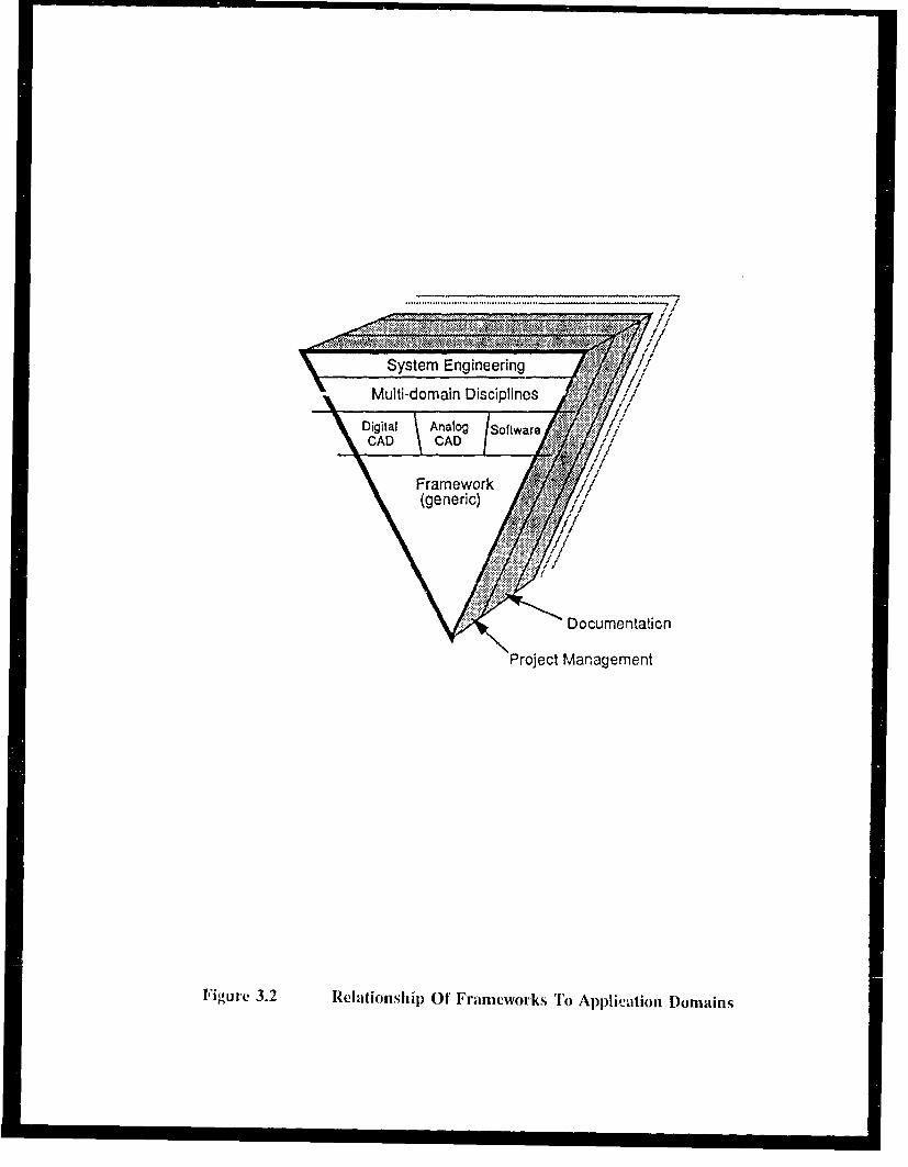
Digital Analog Software ~
... Documentation
Project Management
Figuret 3.2 Relatioiiship1 0f Fraewr h(OIks T'o Applicationi Domains
CHAPTER 3 / DEVELOPMENT TASKS
services to access other data organizations easily. The EIS has developed one domainspecific model for digital IC design.
Results, Accomplishments, and Conclusions: The specification phase resulted in athree-volume document (Reference 3.33) which compiled the feature approaches,language-independent service interfaces, and the information model to support digitalIC design. This material was widely reviewed throughout industry and received positiveevaluations. Incremental builds of these specifications have shown their feasibility andusefulness. EIS is the oihly comprehensive specification of a general purposeengineering framework available today.
The EIS program has had a substantial impact on the development of standardsin the CAD community. Within a year of the program outset, the CAD FrameworkInitiative (CFI) was formed. CH is a consortium of over 50 companies addressing thesame basic scope as the EIS specifications.
The EIS program has supported the CFI in providing strawman candidatestandards and in defining CAD interoperability. To date, the CFI has adopted severalEIS positions and used other EIS specifications as baselines for CFI subcommittees.
The EIS prootyping phase began in October 1989. The purpose of theprototypes is to establish validity of the specifications, determine feasibility ofimplementation, demonstrate that EIS can be built on existing software and adapt toexisting tools, and to provide a vehicle for application demonstrations (EIS in actualuse).
Build One of the prototypes, which has been completed, implements the highlevel object management services suitable for supporting CAD tool attachment anddata interoperability on a local network. In addition, Build One validated the basicobject/function invocation model. A user manual for the prototypes will be availablein January 1991 from Honeywell (Reference 3.34).
The EIS Program held a series of open workshops, the most recent being inNovember 1989. The next open workshop is scheduled for early in FY1991. Anewsletter is published monthly and distributed to a mailing list of 2500 individuals inthe US and abroad.
73
CHAPTER 3 / DEVELOPMENT TASKS
3.2 Test and Life Cycle Support
This section brings together the various VHSIC activities relating to the very importantareas of test and evaluation of the performance and radiation hardness of VHSIC chips, thequalification procedures to insure reliability, and new maintenance concepts needed forVI ISIC.
3.2.1 Test and Evaluation
In-Ilouse Test and Evaluation of VHSIC Chip Performance
Army (ETDL): The Reliability, Testability, and Quality Assurance Branch of theLABCOM ETDL tested and evaluated the following VHSIC chips. The characteristicsof each chip are described in Section 3.4.
Correlator (Hughes) - Parametric measurements were verified on both the correlatorwafer test structures and a packaged device. Functional tests were notperformed due to device tc.,ter limitations. All work was performed betweenMay 1984 and December 1985.
Static Random Access Memory (SRAM) (Texas Instruments) - Electrical performanceverification tests of the SRAM in a DIP package were performed using anon-pipelined mode in a joint effort by ETDL and the Rome Air DevelopmentCenter (RADC). Results of dc tests were in agreement with TI test data. Actest data, however, showed failures in access time and functional operation atelevated temperature. ETDL performed essential electrical characterization on105 SRAM samples in the LCC package including dc and ac parametric testsin both non-pipeline and pipeline modes. Of these, 95 devices were shipped withtest data to Hughes for use in the VI-ISIC Firefinder upgrade program. ETDLcoordinated preparation of a detailed specification in Military Drawing Formatby TI for the SRAM device. All work was performed between September 1984and October 1987.
Multiport Switch (MPS) (Texas Instruments) - Electrical performance tests wereperformed at ETDL and TI. ETDI, coordinated preparation of a detailedspecification in Military Drawing Format by TI for the MPS device. All workwas performed between December 1984 and July 1987.
Static Random Access Memory (SRAM) (Westinghouse) - The chip set was producedjointly by Wcstinghouse and National Semiconductor. Electrical performanceverification tests were performed at E'IDL over the full range of militarytemperature. Functional and parametric test data were in good agreement with
74
CHAPTER 3 / DEVELOPMENT TASKS
manufacturer's test data. All work was performed between August 1985 andNovember 1985.
Arithmetic Element Controller (AEC) (Hughes) - The AEC device was designed byHughes and manufactured by LSI Logic for use in the VIISIC Signal Processor(VSP) module in the VHSIC/Firefinder upgrade. Electrical performanceverification, functional, and parametric tests were performed at ETDL over thefull military temperature range. Test results showed satisfactory performanceand maximum data rates of 33 MHz at 215"C, 34 MHz at -55°C, and 26 MHzat 125'C. All work was performed between February 1984 and March 1989.
Signal Processing Element (SPE) (IBM) - Electrical performance verification tests atETDL showed functional failure at -55"C, and maximum data rates of 22 MHzat 25'C and 26 MHz at 125"C. Failure at low temperature was due to the
presence of electrical noise in the PGA package that increased as temperaturedecreased. Improved functional performance in the PGA package can beobtained with careful test fixturing and installation. In tests performed at ETDLand IBM, the SPE device in the PGA package did not function successfully at
specified frequency and threshold voltage. However, IBM did achieve
satisfactory performance of the SPE chip when used in a comparatively noisefree multichip package. Other problems included a static power supply currenit
(IDD) that exceeded the design specification, and a design problem in theon-chip-monitor (OCM) alleviated by use of a reset sequence in the data inputat start-up to release the data bus. IBM reviewed all of these problems todetermine corrective action. All work was performed between June 1988 andDecember 1989.
Bus Interface Unit (VBIU) (IBM) - Performance tests at ETDL included parametric
and functional. Functional verification at the 50 MHz data rate was not
achieved due to a noisy test fixture. Tests were performed at data rates of 36
Mllz at -55"C, 34 Mliz at 25"C, and 33 Milz at 125"C. All work was
performed between December 1988 and September 1989.
Air Force (RADC): Over the duration of the VIISIC program the MicroelectronicsReliability Division at the Rome Air Development Center performed detailed tests andevaluations of several VIISIC devices. The RADC test facility houses the enhancedVIISIC automated microcircuit electrical test system, the Tester Independent Support
Software System (iISSS) central host computer, and VLSI design workstations. A briefchronology of the electrical testing performed by RADC is described in the following
paragraphs.During FY87, RADC developed test programs and performed characterization
testing on four Vi iSIC device types: tile i loncywcil SCqueiieci, tIe elt, li-sti tilillls
72k SRAM, Westinghouse/National 16k and 64k SRAMs, and the IBM SPE chip.
75
CHAPTER 3 / DEVELOPMENT TASKS
Results of th,: memory device characterizations were documented in a joint AF/Armyreport (RADC-TM-86-5) and were also presented in a technical paper at the 1985Government Microcircuit Applications Conference (GOMAC). See Reference 3.35.Several device performance deficiencies were noted during the testing and werereported directly to the manufacturers to facilitate corrective actions. All device testingwas documented in report form and forwarded to the Army, Navy, and Air ForceVHSIC program offices.
In FY88, test program development and device characterization focused on theIntel VHSIC-like static RAM, MIL-M-38510/613. This was the first VHSIC or VHSIC-like device to receive military qualification status. The characterization included all ac,dc, and functional tests included in the specification along with plots of variousoperating characteristics and a mini-life test on a sample device. The testing performedon the samples obtained by RADC indicated that the devices were able to meet allspecification limits by wide margins and show good long term reliability potential.Results of the characterization were reported in RADC-TM-89-18.
RADC also investigated samples of TRW's CMOS 1028-bit Dual Static ShiftRegister. This device was fabricated using TRW's VHISIC CMOS process. Testingat TRW indicated that the device exhibited high supply currents when certain bits werestored in the shift register. This was confirmed by testing at RADC, and correctiveactions were suggested to TRW in order to eliminate the problem.
Navy (NOSC and NRL): In 1986, functional tests were performed at the Naval OceanSystems Center (NOSC) on Phase 1 CMAC and SPE chips from IBM, CAM andWAM chips from TRW, a 16k SRAM from National Semiconductor, and an FPMAKchip from Raytheon. The IBM, National, and Raytheon parts passed the functionaltests over the frequency range 1-25 MHz at room temperature. The TRW parts werefunctional at 1 MI tz, but defects in the tester adapter board prevented testing at higherclock speeds.
NOSC also performed parametric tests on Phase 1 test chips from IBM, TRW,Motorola, and H loneywell. Measurements included transistor parameters, contactresistance, and resistivity.
In 1987, the Naval Research Laboratory desinged a sidelobe canceller thatincorporated TRW's MAC chip and two personalizations of the Motorola V6000 gatearray. The system ran as designed at speeds tip to 19 MIT/ with simulated data.
ln-I louse Test of VI IDL Phase 2 Clhip l)cscriptions
Navy (NRL J: As part of the acceptance procedure for deliverables, the Naval ResearchLabor,,'ciy (Code 5305) was tasked to test and accept the VIIDL chip descriptionsdelivered on the Phase 2 contracts.
The descriptions delivered by IBM contained non-standard, VI-DL ANSI/iEEE-1076 code; therefore, simulations were not run.
76

CHAPI E~R 3 1 I)EVELOPMENT TASKS
VI IDL (Icwztiptions of the TRW macros wcvre found to fie in error after testingat packaged 11PRAM, for functionality on a Daisy PMX systemn. NRL corrected theInterinetrics V"lIIIA- model of the. 11PRAM and also wrote a correct set of test vectors.The mod'el and the actual part wetec then found to give identical results when runningtho saime set of test vectors.
Elect romnagnetic Efcects (ENME) include upset and damnage from radiated and conductedsources Such ats elect B oMaIgnutic pulse (F-MP), elect romlagnet ic interference (EMI), radiofrequency interference (RH'). high power UnilCtowaVes (I1111M), electrostaiOcdicag(S)a11d lightning. The EINI F Suhcom inittee of the VI ISIC Qualific-, -it Committee investigatedthe p1 ol)1ms associacd with estbl~ishing, sianrdards for testin n acccpting VII[SIC devicesJor military sistems Results were prescnted in the NMF! Subcmimittee report, Reference
I [31MWfjfilLeioanicIetsCM The 11I HNOI\'[SIC Phase 2 Final1'cchnicAl Report (Ruecrcnwc 3.45) states that (at) protection against electromagneticpulse (FNl) is at system problem and cannot be resolved at thc chip level, and (b) IBMhas demnnsi rated elect 051 at ic dis'charge kE'SI) protect i .r exceeding 800 V (hurnaitbody mode) on packaged VIIS iC chips. After lPhasm 2: work continluedl on ESI)
uImotect ion New I [3M designs were ma ut'act ured am' eva]utiatd using the VI [SICCPhase 2 piotcess. 'Ihcms ewIC'~ (leSiglis1 Offere ne~gligibIle perf0ot mane1C dugradation andUn 1ovidled protect ion level capability of up to 41000 voltzs.
A ':st Fr~ Evlutio of VI ISV'(i ailinIlrns
VI ISI( Q ch arc ie ba :qi totpvivie K~cnn emburimms sshih suWct them L
ii ti kar and sp";v radiation thrmta s: total dosc (ID) S clccsLcArIon dam-age: i(iaetrupset and latchuip (LU); ioniiiintq levecl A~ -i strvinability ml sii( ueetUpu tJ
"pro'ie'1ced by alpha ' t jZtidesN, protoZns, amd hcxavy ions. ]In Scct ion 3.3.2 (1IBM) and Section3'x.~.sveral1 of th e 5 m proc" mfve in ten"'s to e:nhance radial ion ha~rdness -.re described. The
)!e~iIsection giveN' the, I e.nl ts of the fadiation hardnecss tsson Phase I chips. D~etails of1wtest proced ires ai '2 giveni in the 119ýS7 VIISI ( Amiua tt Re poritIRefer cnec 2,28, Sect ion
X" U he results At the rhaiaon tests lot I13M Phabe 2 chips are gwiei in S, 1332.I lhe test chp that wcie usecd to denintoitsr. m the radiation hNOW -i ac . in the
1ŽNi\ VI ISI( IL-,t:xt'nsiim-I(-.si);c-te poouiar~n arc h!'ltcd iin !Ne toIlox~i: IAL
77
CHA;TER 3 1 DEVELOifl'ENT TASKS
Contractor TechnolopD' Test Chip Radiation Test*
Westinghouse/NSC CMOS 10k gate arrayl64k SRAM AllMotorola CMOS Discrete transistors TDIBM NMOS - CM/OS Macro 11 test chip TD/SEUHughes CMOS/SOS Test structures TD,SEUHarris/GE/RCA CMOS/SOS 64k SRAM AllHoneywell Bipolar SEU test chip SEUTI STL, ACS chip LUTRW Bipolar Macrocell test chip LU
T D =total dose; SEU = singlcecvent upset,, LU = latchup
WestinghoLISe: Trhe SAFE implant used b,, Westinghouse in hardening its gate arrayswas also used with thle 64k SRAM%, but the recessed n' change was not implementedinitially dlIc to the, Magnitude Of the layout' chan1ges that would have been required.A\ scherrte to incorporate thle recessed ný design into the SRAM was developed byNational Semiiconductor Corporation in a subsequent IRAD program. Without thlefully1 recessed n+, the SRAMI demonstrated it total dose hardness capability between 100
and '00 kilorads, With the recesscd ri' Valm~td the 61yk SRZAM was hardtmcgarad. The 10k gate array fabricated at Westinghouse was also hard to 1 megarad.
T1he use of p1 o1 p, cpitaxial substrates eliminiiated dose rate induced latch upaind led to an~ inlprovernenlt in the dose rate upset t hreshold from Ix105 iads/s tobetween 700 aml 'Irid Oit rads/s. H eavy ion SEU tests showed that the SRAM'sprojected error rate wvas reduced from 1x1()-5 to 5x 10⁶~ upsets/bit-day by the epitaxialSubstrate, and then to less than 5xlI ( upsets/bit-day by incorporating cross- "oupledresistors in thli SRI\NI mem~ory cell. These- values are based onl room teinperat lireoperation at 3.0 volts. At 5.0 volts. the SRAM improved to less thant 1x10' 0 upscts/bit-day, wýhile t lie. gate a mvy with no0 SFU. hardeninig wvas characterized by an error rateof 5XltV' upse"ts/bit-day.
IBMN: Following thle VI ISK l(' Phas 1 programi, I113M tranI1Sit 0iond theit radiationhardening activities to a1 1-25 in irofi h a 1k (M(IS r'roý:ss. '[his technology had beeninstalled as part of thltir slifrtcgy 10 P'OII0 odnee suom vron (NIUSi under Vi iSI( P 1hase 2.C'M(S also bcaimec thlv IBMN 1.25 111 eoit tvchnology aind hlas beniefited from theradliatIion hat deni ti activitiesý dum iig tie \'lISI l( PaSo 2 and C VSC pr" grainls. T]heI 13M Phlase 1 (CM ( s tc~hniolojiy is harid to 1 mega rad total do)se and 1 x10') rads/s dloserate uipset I hieslaId: ILess. tliat 1 xV "' l tipwSel/h1i-t-y Sl-LJ Is .tvailable; and it has no0
lat ei ri. 11 NI hs I ced t k Sl( i N-I it i tlls tech njoll gy aj~ ISd Is dVelopi :ig a 256kSR,\icti. 13 II " -,d cd01 N
CHAPTER 3 / I)EVEL0PMENT TASKS
Hug~hes Aircraft Corporat ion: CMOS/SOS correlator chips produced by Hughes duringthe regular Phase 1 program miet or exceeded space hardness levels, especially in tileareas of dose rate upset and latchup, where the use of SOS offers intrins ic advantages.In total dose testing, the correlator remained functional uip to doses of 2 to 3 megarads,but leakage currents became significant at several hundred kAilorads.
11arris/GE/RCA: Total dose tests have shown that the CMO0S/SOS 64k SRAMfunctionality is maintained to several tens of mnegarads. However, further work isneeded to reduce standby current which becomes significant and saturates afterapproximately 100 krads. Dose rate upset hardness has been demonstrated to mlorethan 2x10 11 rads/s, while SEU testing with heavy ions under normal bias conditionsproduced no upsets at effective linear energy transfers up to 250 MeV/(mg/cm 2 ), whichmakes it effectively immtune to cosflri ray upset.
At the present time, Harris is fabricating thle 64k SRAM along with 1.25 mi1crongate arrays and custom chips in thle CMOS/SOS process. Thus, -a spectrum of radiationlhard SOS chips is currently available.
TRW: Content Addressable Memory (CAM) chips were processed along with a testchip containing about 200 special structures for studying latchup effects. Process lotsincluded standard hulk, 7 micron, 10 micron, and 15 micron epitaxial starting wafers.CAM,; manufactured onl 7 micron epitaxial substrates exhibited no latchup responsesat (lose rates up to 2xl0'(' rads/s with supply voltages as high as 7 volts. PISCESmodeling, coupled with bench characterization of thle test structures,, revealed that the7 micron thicknoss was optlimum for preventing latchup in TRW's triple difftusedbipolar process. TVhese substrates eliminated latchup without de-rcasing manufacturingyield or perfOrmiance.
3.2.2 Test 'lechnology
11-V.- Fester I nd Uerllenoe Support Software Syste i l'IS$
Thre TISSS is a syste ni for the a uromated generation and mlaintenianec of electrical"sptcitications and test programls for (livital mie1rocircuits. The use of the TISSS requires thleChip decsignecr to address, at at very early stage ini thle design, thle question of flow thle desired]tiunet ional ity capit ured In thec de-sign Is to he tested. The lack of coordination beitween thetune' oion a speci ficat ioiis and( thle specificatlonls for' test waIs becomling a serious problem withIh'. advenlt of i nereasinrg Chip c( mplcxi ty. F urt he imore, thle pirepara tion of test vectors waseqaiculii! rig a ar" 'ffort and had "o be t 'lgCted to at parlticular tester.
J1 Syste il r11Id LeIs at da~ti1abase-eCutere~d software!- suppojrt systeml that P-, i n(ICpen(IC-ntot hothI the comlputer aided dcsigr and test curvi rollments and informiation represeniltation
* '''Sfor t:t\ct!!a~t 1.111 a N' tI "rv -cific.1rim ion iror mttionl to accolmnlish its
*79

CHAPTIER 3 / I)EVELOPMENT TASKS
aiutomation goals. These languages are currently undergoing standardization within the IEEEdesign and test communities.
The capability provided by TiSSS enables the user to develop and maintain complex,device design and test information in a standardized, transportable computer-accessible formatthat can be used to automatically generate test vectors for the device into the data formatappropriate to the tester being used. The Government use of TISSS significantly reduces thetime required to insert advanced technology microelectronics into operational systems. Inaddition, the device data stored in the database can be used for reprocurement of devices nolonger being manufactured.
Full scale development of TISSS was begun by the Harris Corporation in September1985 and software development and initial application to the Generic VI-ISIC SpaceborneComputer (GVSC) microcircuits was completed duiing 19891990. This initial use of TISSSwas for the generation of electrical test specifications and test programs for the GVSCmicrocircuits developed by the Air Force Space Technology Center (AFSTC). During thisdemonstration and application, the GVSC contractors, Honeywell and IBM, utilized TISSSsoftware installed at their sites for the generation and capture of electrical test specificationsfor their respective GVSC microcircuits. They also translated test vec.tor information to theTISSS Vector Language (TVL) for submission to tho TISSS data base. After this informationwas generated and captured, it was then sent to the Rome Air Development Center for auditusing the TISSS located there. After auditing, the information was used to atutomaticallygenerate test programns foir all of the GVSC microcircuits. The use of TISSS reduced the timeiceded( to generate these complex GVSC test programs from an estimated one man-year to
two man-weeks. The test programs were generated using the newly completed TISSS Teradyne1953 postprocessor.
Following the successful demonstration and application of TiSSS in the GVSC1Program, AFSTC required that the TISSS methodology be used in microcircuit developmentwork to be performed by the Advanced Spaccborne Computer Module (ASCM) Program.Uind,-r this program, TISSS will also be appied to support design and test information captureaid automatic test program generation for digital boards developed by the ASCM Program.
In 1990. the TISSS program will coniplete the development of a generic postprocessorthat will greatly enhance inidustry acceptance of the TISSS data standards and practices. Thegeneric postprocessor will reduce the tinme and cost associated with customizing the TISSSpostproccssor to work with new target mici ocircuit and printed circuit board testers. The"T'ISSS generic postproccssor, like the rest of the TISSS software, is coded entirely in Ada.
In addition to thie 'ISSS applications to digital microcircuits, TISSS is currentlyundergoing extensions to support digital line replaceable modules (LRMs) targeted fol nextgeneration aircraft platforms, such as the Advanced Tactical Fighter (ATF). The TISSSextension dcvelopment is currently supported by the A'TF Program Office. The TISSS will be(Cl01)nstratCd during the summer of 1990 with applications to LRMs targeted for the ATF.Sl,,i dcmonstratioll will consist of the capture of design and test information for Integrated
('ommtunication Na'igatlion Identification Avionics (ICNIA) LRMs and auditing of theintormation using 1ISSS. After automatic auditing by TISSS, the information will be used toautomatically generate test programs tfor two target testcrs, one located at RADC and the
80
CHAPTER 31 DEVEILOPMENT TASKS
other at the Sacramento Air Logistics Center. This demonstration wil! show the functionalityof TISSS as applied to digital LRMs and also the feasibility of the capture and use of designand test information for LRM production, integration, certification, and life cycle support.
The HISSS information standards used are the VI ISIC Hardware Description Language,discussed in Section 3.1.3 of this report, the; TISSS Vector Language (TVL), and the TestDescription Language (TDL). VIIIDL was standardized by the IEEE as ANSI/IEEE1076-1987. The TISSS TVL is currently undcrgoing IEEE standardization and will be calledthe Waveform and Vector Exchange Specification (WAVES). The Test Description Language(T[DL) is beginning TEEl standardization and will he called thc Test Specification Language(TSL). The successful standardization of thuese representations will fulfil! the VHSIC goal ofdefining the information languages for representing and easily interchanging for use allinformation necessary for microcircuit design, manufacture, test, insertion, and life cyclesupport. See References 3.37-3.41 foi additional information on 1ISSS.
Microcircuit Tresters
The Rome Air Development Center (RAI)C) is the lead organization responsible forthe generation of specifications for qualification testing of integrated circuits used by DoD.Accordingly, they have been concerned with the capability of available testers for testingVI ISIC-class devices.
At the start of the Vl ISIC program it was clear that existing microcircuit testers wouldnot be capable of adequately assessing the quality of Phase 1 VIISIC chips. For example, agood portion of the earliest electrical testing on VIISIC Phase 1 memory devices wasperformed on a Tektronix S.3270 automated tester. The S-3270 had the capability of testingdevices with up to 64 I/O pins at speeds up to 20 MI'z. H lowever, it did not have tileperformance necessary to test the majority of VI ISIC devices. Electrical testing was thereforetransitioned to a GenRad CR-18 capable of testing dcvices with up to 288 pins and clock ratesup to 40 MHz with patterns of up to 256k test vectors.
RADC surveyed the tester manufacturers arid it was apparent that even next generationtest equipment would not have the necessalv performnancc for characterizing Phase 2 VHSICdevices. Therefore, a contract was initiated with GenRad to develop a VIISIC-classmicrocircuit tester in 1984.
I lowever, GenRad decided not to continue in the tester business. In fulfillment of theircontract, however, they did deliver and install at RAI)C a Tleradyne .1953 tester which metRAD(;'s requirements that it be capable of testing 100% of VI-ISIC Phase 1 devices andapproximately 85% of VIISIC Phase 2 devices. It is capable of uncompromised testing ofdevices with up to 256 1/O pins at data rates up to 5.0 Mllz. By multiplexing adjacent pins,the J953 can test devices with clock rates up to 100 MlIz. The J953 can place timing edgeswitl, an accuracy of 500 ps and apply patterns to the device of up I - 4M vectors. The testhead hl s very low capacitance (301 pl") which lends itself to accurate waveform reproduction.
Of equal implortance with the hardware, is the capability of the software that can beused with any test system. A 'IISSS postproccssor for the J953 makes it possible to generate
81

CHAPTER 3 / DEVELOPMENT TASKS
entire test programs for complex devices in a few weeks instead of the several months that hadbeen required in the past.
3.2.3 Reliability and Qualification
Introduction
The reliability of integrated circuits has always been a serious issue for thesemiconductor industry. Military requirements have further necessitated the establishment ofqualifying procedures and standards, in order for parts to be used in DoD systems. However,as devices of increasing complexity, requiring new and complicated fabrication processes aredesigned and built, the problem of assuring their reliability becomes more difficult. The costof qualifying parts becomes an important consideration that in turn depends on their demand.
The VHSIC program attempted to address these problems with a three-fold approach.The first encouraged Phase 1 chip suppliers to demonstrate the use of the existing qualificationprocedures. These procedures are:
"o the certification of the production line (fabrication, assembly, and test procedures)in accordance with MIL-STD-976 to assure a controlled manufacturing process,
"o characterization and documentation of of the device in a dated specification (calleda "slash sheet") in accordance with MIL-STD-38510, and
"o testing of a designated production lot in accordance with MIL-STD-38510 and MIL-STD-883C procedures.
Devices which satisfy these recquilements are put on a Qualified Parts List (QPL). Thestatus of these procedures as of December 1988 are given in the 1988 VIISIC Annual Report(Reference 2.29). More recent additions to the QPL are given below.
The second approach was to support the development of improved test methods,reliability prediction models, and software tools. Early contracts are listed in Appendix B(Early Phase 3 Projects, Section 8). Contracts completed after 1986 are listed in Section 3.2ot iAppendix 13. Two of these arc discussed below: Reliability Assessment of Gate Arrays andReliability Prediction Modeling. The TISSS project has already been discussed in Section3.2.2.
The long lerm approach was to develop a set of generic qualification procedures thattake advantage of test areas on the VI ISIC chip, separate test chips, and separate test wafersto conitrol and document the extremely complex fabrication process. The design proceduresarc also subject to certification. Manufacturers whose fabrication, design and controlprocedurcs mect the requirements have their facility placed on the Qualified ManufacturersIlist (Q M I'.).-
82
CHAPTER 3/ DEVELOPMENT TASKS
Reliability Assessment of Gate Arrays (GTE)
This project by General Telephone and Electronics focused on the generic qualificationof gate arrays and the reliability of representative products. The final technical report(Reference 3.42) contains the contractor's results of step-stress, life tests, and failure analysisdone on CMOS standard evaluation circuits. The current military specifications for gate arraydevices require a Standard Evaluation Circuit (SEC) to be used to assess the quality andreliability of a manufacturer's gate array family. The concept behind the SEC is to runexhaustive reliability tests and characteriLe the electrical parameters of one device whichrepresents the design rules and macruceii library of a particular technology and array family.Subsequent designs in the same family would not require the life tests and qualification screensspecified for all QPL devices.
This program defined the recommended circuitry for CMOS and ECL SECs. Toevaluate the effectiveness of current military requirements, the SECs of two manufacturerswere tested. The SECs were electrically characterized and the results summarized. Reliability,step-stress, and life testing was done on a CMOS SEC to validate current test methods. Thefailure mechanisms studied were electromigration, hot electron effects, and dielectricbreakdown. The program concluded that current high temperature life testing and burn-intesting are adequate to detect any electromigration and dielectric breakdown problems. Theprogram recommended dynamic low temperature life testing of SECs and dynamic lowtemperature burn-in of production devices to monitor hot electron effects in CMOS devices.Also, a list of desirable features for computer aided design (CAD) tools was developed.
Reliability Prediction Modeling
IlT Research Institute (IITRI) and Honeywell SSED were teamed under Contract.t30602-86-C-0261 to RADC/RI3RA to develop a reliability prediction model for fielded CMOSVIISIC and VIISIC-like devices. Since little or no field reliability data was available, anapproach was taken that used methods which dcviatcd from the traditional statistical analysisof field failure rate data. Two models for predicting failure rates for VHSIC and VIISIC-like CMOS microcircuits were developed: a detailed model and a short form model.
The detailed model is based on the characteristics of specific failure modes, manufactrerspecific information such as defect density, wearout performance, and key application datasuch as temperature and operating time. The short form model is 1, condensed version of thedetailed model and does not require manufacturer specific informatio.A, but uses easilyaccessible information. The penalty in using the short model is its lower precision andaccuracy relative to the detailed model.
Thz rnodels account for both time dependent and defect-related failure mechanisms.A data base was built containing the life test, burn-in, and environmental test results from avarietv of manufacturers. Much of the da(a contained in this data base was used in thequantification of early life failure rates for various specific failure mechanisms, Therefore, the
83
CHAPTER 3 / DEVELOPMENT TASKS
detailed model, in predicting defect-related early life failure rates, yields an industry widerepresentative failure rate. The use of actual defect densities, if properly measured, will resultin predicted reliability values which are more precise and accurate than conventional regressiontype prediction models.
It was also determined in this study that it is these defect-related mechanisms that drivefailure rate in the part's useful life. Wearout mechanisms were also modeled which willprovide an approximate end of lifetime as a function of the part's design rules and itsparticular application.
The model addresses three time-dependent mechanisms: electromigration, time-dependent dielectric breakdown, and hot carrier effects. The model has factors for chip area,defect density, and/or minimum feature size so that changes in technology can readily befactored in. It has a correction factor to modify the model as VHSIC field experience becomesavailable and to modify the model for a particular fabrication process based on the availabilityof high quality life tests. The model can also utilize test pattern data from manufacturers inconjunction with the Yield Enhancement and Generic Qualification programs. There is apackage factor which considers the numbcr of package pins and includes the following packagetypes: pin grid arrays, chip carriers, and dual-in-line packages. It also has factors forEOS/ESD and whether or not the device is on the QPLUQML.
The detailed model was validated with life test data that was available on 1-0 and 1.25micron feature size devices from three separate manufacturing processes and both models wereproposed for inclusion in MI.L-HDBK-217 "Reliability Prediction of Electronic Equipment."The final report, (Reference 3.43) was circulated via an extensive mailing list. The modelswere well received and should prove to be very useful DoD/industry tools.
Qualification Procedures
As the VIISIC chips were being designed, developed, and produced, it becameincreasingly clear that the QPL procedures for qualifying them for military use were noteffective and would become even less so as time progressed. Because of their functionalcomplexity, the chips were much more application-specific than the standard logic or standardmicroprocessor chips used in the past. In addition, the dense, fine-line features of the chipsmade standard optical inspection and electrical testing ineffective in screening out the faultyor marginal ones. Finally, the cost of qualifying a specific part was sufficiently high thatqualification was undertaken only if the part were assured of use in a large procurement. Thecurrent status of QPL is given below and the alternative Qualified Manufacturers List (QML)procedures are discussed.
Qualified Parts List (OPL): The present status of manufacturing line and chipqualification, conducted under the Defense Electronic Supply Center (I)ESC) QualifiedParts List (QPL) guidelines, is described below.
84
CHAPTER 3 / DEVELOPMENT TASKS
Westinghouse
o A 1.25 micron (0.9 eff) CMOS 5 V gate array line was certified underMIL-STD-976 and MIL-M-38510, effective December 20, 1989.Included in this certification is the gate array design system, inaccordance with the "generic" gate array certification/qualificationmethod of MIL-M-38510/608.
o The Parametric Monitor (PM) design was approved January 12, 1989by RADC and DESC.
o A Standard Evaluation Circuit (SEC) was approved on May 31, 1989by RADC and DESC. This will serve as the qualification test vehicle,per MIL-M-38510/608 for a gate array family. The family consists of54k, 28k, 20k and 3k gate arrays.
IBM
o 620 SPEs were qualified to MIL-M-38510, effective June 1990.
Qualified Manufacturers List (OML): The goal of the QML program is to developstandards more appropriate for qualifying VFISIC chips than the traditional procedures.The new standards are based on establishing qualified manufacturing lines that canproduce fully qualified parts without the costly testing of each individual part.
Surrogate devices are used for controlling the process and revealing quality problems.CAD tools are fully integrated into the ceitification procedure and chip families andpackaging techniques which apply to more than one device are dealt with generically.This process of "generic" qualification for military products also depends on tightcontrol of the manufacturing process in order to assure that the quality and reliabilityof the product, once established, remain within required limits.
QML is a long term effort that is expected to continue beyond the VHSICprogram . A joint DoD/Semiconductor Industry Association statement announcing thisnew strategy for military microcircuit manufacturing and procurement was released in
February 1989. Ten major semiconductor companies participated in the refinement ofthe requirements originally developed under a VIISIC contract. These were AT&T,Ilarris Semiconductor (3 locations), IBM, Intel, LSI Logic, Nation:ll Semiconductor,Texas Instruments, and VLSI Technologies. The result of this effort, MIL-1-38535"General Specifications for Integrated Circuits (Microcircuits) Manufacturing", wasissued on I)ccember 18, 1989. These companies are now in various stages ofpreparation for certification validation reviews bascd on the MIL-I-38535 requirements.Certification validation reviews were conducted at A I&I and Intei. - he A F&T[(Allentown Pa) 1.25 micron UMOS process was certified on l)ccember 19, 1989, and
85
CHAPTER 3 / DEVELOPMENT TASKS
full AT&T qualification was completed during the first quarter 1990. Similarly, Intelcertified their 1.0 micron CMOS process in February 1990 and received fullqualification shortly thereafter.
Efforts to include linear devices and GaAs technology into the QML concept arecontinuing. Through the MIMIC program, industry working groups have beenestablished to address the QML requirements for GaAs circuits. Customer generateddesigns will be addressed in future updates to MIL-I-38535.
0.5 Micron QML: A 24 month modification to the IBM Phase 2 contract was awardedon June 1, 1988 to extend the QML procedures to 0.5 micron technology. Theobjectives were to (1) develop and implement statistical process control (SPC)techniques; (2) design and implement process control monitors and standar evaluationcircuits as in-line process monitors and reliability indicators; (3) develop a reliabilityprediction model; (4) validate the model lthrough testing; and (5) certify and qualifythe 0.5 micron CMOS process for inclusion on a qualified manufactuners list.
IBM has implemented a statistical process control program, as per JEDCPublication 19. A VIISIC/VLSI reliability model was completed and released to thePhase 2 program office. The screening and life test results for both the 1.0 micron arid0.5 micron CMOS signal processing clement (SPE) chips matched the modelpredictions.
3.2.4 Maintenance Concepts for VHSIC
Honeywell performed a study of the impact that advanced microelcctronics technologywill have on the development of appropriate maintenance concepts. This study identified andcharacterized the maintainability and diagnostic problems that might occur in advancedmicroelectronic systems. The guidelines are useful for specifying realistic maintenancerequirements and for designing systems to meet those requirements. The guidelines are writtenfor the system, module, and chip levels of assembly and generally provide options for thedesigner to choose which are most appropriate to the task. They were developed with theknowledge that VIISIC characteristics, such as built-in-test, might mitigate the problem.
System level guidelines include a discussion of maintainability as a primary systemrequirement, equal in importaacc to the mission requirements of that system. Diagnosticinformation management, packaging, fault diagnosis techniques, and VIISIC-1 and VHSIC-2i maintainability features are discussed.
Module level guidelines cover the electrical and mechanical characteristics associatedwith the maintenance features and the use of built-in test and automatic test equipment. Therolc of the modttle level (liugnost ics as a link between chip and system processes is stressed.
Chip level guidelines focus on methods used in the desigii of chips to implement ahierarchy of mailntcnance diagnosis throughout the system.
* ~ ~ ~ ~ % t*ttli a.lý1 .~j~~lJ~ ~ 1 1n114iCs -f good cý-g fo rnna a.Wnant an
the tradeoff betw%ecn the level of ma iiitaiinability achicvable and its associated cost. Several
86
CHAPTER 3 / DEVELOPMENT TASKS
appendices, which contain detailed examples of diagnostic techniques, are included in the finalreport for this project (Reference 3.44).
67
CIHAPTER 3 / DEVELOPMENT TASKS
3.3 Chip Fabrication
The following assessment of the impact of VHSIC on fabrication technology has beencontributed by one of the program managers intimately involved in the development of thePhase 2 VHSIC "superchips" which successfully pushed the prototype production of highdensity, large area, one-half micron silicon fabrication technology to its limits.
The Impact of VIISIC on Fabrication Technology
Charles S. MeyerMotorola
My involvement with the VHSIC Program started at its beginning in 1979.I helped prepare our Phase 0 proposal with teammates TRW and Sperry Univac,and I continued to work on the Program throughout Phase 1. I rejoined theTRW/Motorola effort as Motorola's Program Manager during the last two yearsof Phase 2 when it returned to our Advanced Products Research and DevelopmentLaboratory (APRDL).
What has been the impact of VHSIC on microcircuit fabrication technology?It is my opinion that it has served as a significant accelerating factor in ourprogression to successively denser integrated circuit generations.
The thrust of VHSIC technology was intended by the Government to beleading-edge in nature but firmly positioned in the mainstream of projectedintegrated circuit fabrication trends. This was true in Motorola's case becauseprocess/device development at both the 1.25 micron (Phase 1) and 0.5 micron(Phase 2) CMOS technology levels was planned and would have occurred withoutVHSIC. Even with VHSIC, Motorola paid for the process development activitiesitself. However, the Program provided us with the opportunity arid funding toexercise these processes on real circuits earlier than would have otherwise been thecase and to do this with schedule demands that forced the hard decisions necessaryfor yield enhancement.
An example from our Phase 1 experience was the use of polycide (the gateelectrode material comprised of a sandwich of a polysilicon and low resistancesilicide). We had developed the polycide process module and used it on aprototype commercial memory chip before employing it on our VHSIC circuit. TheVHSIC design, in turn, arrived somewhat ahead of a commercial microprocessorpart that was also scheduled to use polycide. This microprocessor's topographywas closer to that of the VHSIC circuit than the memory and thus we got a jumpstart on exercising the polycide module in a "logic" process. Both circuitsbenefitted, I think, from subsequently being run in parallel.
In the case of Phase 2, we have conclUded that the presence of VHSIC inAPRIL accelerated our progress on 0.5 micron technoiogy by almost a year. Wehad to redirect our internal resources to meeling the incredibly challenging demandsinvolved in assembling a 0.5 micron, salicided-transistor, triple -- level-- metal
CHAPTER 3 / I)EVELOPMENT TASKS
technology and successfully using it to fabricate 1.5 x 1.6 inch dice. Motorola'splanned purchase of a high numerical aperture stepper had to be expedited andmastery of the equipment was accelerated by the need to perform optical stitching.Again, although this developmental work was funded by our company, the VHSICtime schedules forced us to "make way" sooner for this generaticn of technologyand also provided the circuit vehicles to exercise it and measure progress. This 0.5micron technology is being transferred to TRW under a separate contract forcontinued application to the Government projects.
From a more global perspective, apart from the hardware aspects, I feel thatVHSIC has accomplished another important mission by facilitating the interactionbetween semiconductor technologists and military electronic equipment designers.As a result of this program, each has a better understanding of the other'scapabilities and limitations. It is my expectation that success in future applicationswill show this to have been a major benefit of VHSIC.
3.3.1 1.25 Micron (Phase I and Yield Enhaicemient)
Introduction
The six contractors usd• several different fabrication technologies and each had differentbaseline processes. Thus, although there were some common problems. for the most part eachcontractor had to overcome a different set of obstacles. In every case, these processingdifficulties were overcome and chips were successfully produced.
The fabrication goal of the VIISIC program was to develop a process which couldproduce complex 1.25 micron chips at a 10% or greater packaged yield so as to be affordablefor use in military equipment. The process was to be well characterized and controlled so asto produce consistent yields. Tlhe chips were required to be very reliable in the hostileenvironments experienced in battlefield conditions.
For many of the Phase 1 chips, these targcts could not be reached initially. Therefore,at Yield Enhancement cffort was undcrtakcn as anl addition to cach of thle Phase 1 contracts.The goal was to ccnter the process parameters to mnaximize yield and reproducibility. A targetvýlue for the yield of packaged chips was set at 10(li,. [he yield inhibitors had to be identifiedantd corrected by changing the manufacturing proccss. Progress toward tile stated goal wasmeasurcd by periodically running three consecemi ive' lots nominally consisting of 20 wafers each."Ihesc three lots weClc collcctivcly tcrmecd at Yicld Verification Run ( YVR). Yield at variouspoints in the process was measured and compared to interim goals. The yield inhibitors wCreidentified and listed in their imnportamce to Nield loss. Tlhis deter ntincd the arcas on which the,ork conllcltrated during tihe next pil iod. S ttr mar lIes for e;ach lcontractor', yield enhance ment
progran, are included below. Further details caln be found in, Refercnlle 2.27.
N9
CHAPTER 3 / 1)EVELOPMENT TASKS
I loneywell
Honeywell used an advanced digital bipolar (ADat 111) fabrication process throughoutthe Phase 1 and Yield Enhancement programs. It is based onl dielectric isolation, an ionimplanted buried collector layer with sheet resistance 3 to 5 times lower than the originalpolysilicon buried layer process, and three layers of metalization for interconnections.
Maintaining a semii-planar oxide dielectric process greatly improved the integrity of themetal interconnection layers. Metalization coverage over "steps" in the underlaying insulatorlayer was enhanced by sloping the walls of the vias with a well controlled etching process.IBuried-layer to buried-layer current leakage was reduced by modifying the KOH etch depthand by routinely monitoring the autodoping from the heavily doped buried layer. Thlestandard dielectric process was replaced by a bias sputtered quartz process to improveplanarization for better metal step coverage and to reduce mectal streamiers during the etchcycles.
A serious problemn manifested itself in the form of ,evere crystal defects in the cn-itterstructitre of the bipolar device after the emitter anneal. 'These detects were traced to -in effectby the ton implanter. '[le problem was eliminated by replacing the arsenic pentafluoridesource gas with arsine source gas.
Variations in metal line width resulted from reflections from thle surfaces during maskalignment. An anti-reflective coating of poly'inide/dve va~s develoncd to solve this problem.'['his process also helped to reduce particle co!.!amination and to .,.prove the cycle timec.
All of these process improvements led to a defect (len-t', i:. the V1 ISIC pilot linle lowenough to allow the fabrication of fully fntMC1iona hrassboard chip1s. I lowevCr. even thouPghthle process could produce. ful K ftinct ional chips, the yield was below the target package yieýldof 101%.
At the beginning of the Yield Enha neement eftort (1984) the major yield inhibhitorswere., iii order of de~crcaisintz sevecrit:
1. Collector-to-e nMCIte 'pipes'2. Schottkv diode lea kaoze
3.Pai tictidatcs In the equipment1C11 ew irnmerllit
I y Apr i 1986, the cot espotiding 11"t ws
1. Particullates2. 1 1mlat~ltg/edgf- detects
3.1 ttell~r la n mtalhos4. Mcletl "st nalllcts'5. 1Pi1pus
A,, ''an be seen. t\kt) Nears of c0rh'Crrtrat1tl cttol 0I] on1 thepoblem) ot pipeJS pus1'hed it to t11ehot toim of the l1It. As l tIimm \%0 110\ (A .thr o lhlom'. I Iih' rljflfl. kA111 novi thlk , lim hill
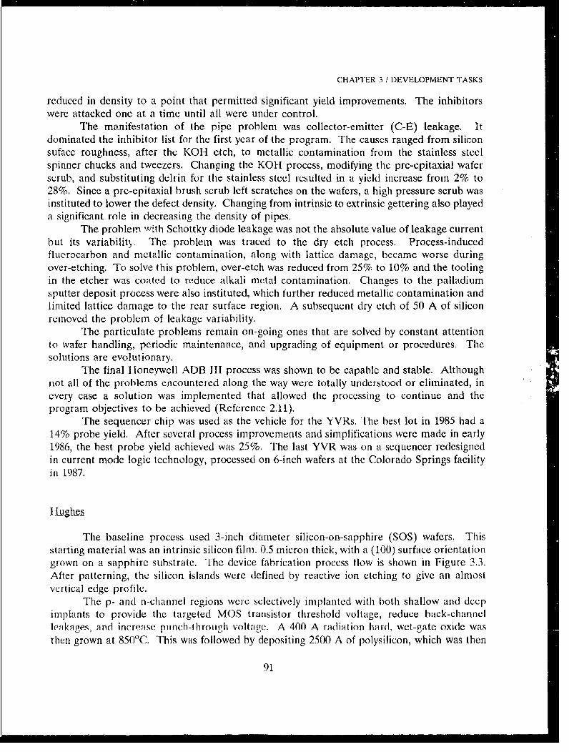
CHAPTER 3 / DEVELOPMENT TASKS
reduced in density to a point that permitted significant yield improvements. The inhibitorswere attacked one at a time until all were under control.
The manifestation of the pipe problem was collector-emitter (C-E) leakage. Itdominated the inhibitor list for the first year of the program. The causes ranged from siliconsuface roughness, after the KOH etch, to metallic contamination from the stainless steelspinner chucks and tweezers. Changing the KOH process, modifying the pre-epitaxial waferscrub, and substituting delrin for the stainless steel resulted in a yield increase from 2% to28%. Since a pre-epitaxial brush scrub left scratches on the wafers, a high pressure scrub wasinstituted to lower the defect density. Changing from intrinsic to extrinsic gettering also playeda significant role in decreasing the density of pipes.
The problem with Schottky diode leakage was not the absolute value of leakage currentbut its variability. The problem was traced to the dry etch process. Process-inducedfluorocarbon and metallic contamination, along with lattice damage, became worse duringover-etching. To solve this problem, over-etch was reduced from 25% to 10% and the toolingin the etcher was coated to reduce alkali metal contamination. Changes to the palladiumsputter deposit process were also instituted, which further reduced metallic contamination andlimited lattice damage to the rear surface region. A subsequent dry etch of 50 A of siliconremoved the problem of leakage variability.
The particulate problems remain on-going ones that are solved by constant attentionto wafer handling, periodic maintenance, and upgrading of equipment or procedures. Thesolutions are evolutionary.
The final Honeywell ADB III process was shown to be capable and stable. Althoughnot all of the problems encountered along the way were totally understood or eliminated, inevery case a solution was implemented that allowed the processing to continue and theprogram objectives to be achieved (Reference 2.11).
The sequencer chip was used as the vehicle for the YVRs. The best lot in 1985 had a14% probe yield. After several process improvements and simplifications were made in early1986, the best probe yield achieved was 25%. The last YVR was on a sequencer redesignedin current mode logic technology, processed on 6-inch wafers at the Colorado Springs facilityin 1987.
Hughes
The baseline process used 3-inch diameter silicon-on-sapphire (SOS) wafers. Thisstarting material was an intrinsic silicon film. 0.5 micron thick, with a (100) surface orientationgrown on a sapphire substrate. The device fabrication process flow is shown in Figure 3.3.After patterning, the silicon islands were defined by reactive ion etching to give an almostvertical edge profile.
The p- and n-channel regions were selectively implanted with both shallow and deepimplants to provide the targeted MOS transistor threshold voltage, reduce back-channelleakages, and increase punch-through voltaie. A 400 A rtdiation hard, wet-gate oxide wasthen grown at 850"C. This was followed by depositing 2500 A of polysilicon, which was then
91
1. MARK LAYERS
I ' ,,' t _ J - - iSi (0.5 pm )
"2. SI ISLAND MASK/ETCH A12 - - ." (033. P-MASK/IMPLANT -034. N-MASK/IMPLANT ,- r
. .- -- Ta Si25. GATE OXIDE POLY[~6. POLY/TaSi 2 DEPOSITION GATE OXIDE
.,• .-----. '=-RESIST
7. WINDOW MASK i POLYCIDE
8. POLY MASK/ETCH 7777-7
9. WINDOW MASK (10. P+ MASK/IMPLANT F N P 111. N+ MASK/IMPLANT ____ .._._C
12. SILOX DEPOSITION J.\.•./...Si 0213. WINDOW MASK
14. CONTACT MASK/ETCH / / / ',,/,, ?
15. AL/1% SI SPUTTER AI/Si16. WINDOW MASK - .L ..°17. METAL MASK/ETCH .....- A12 03
Figure 3.3 SOS-Ill VHSIC Phase I Fabrication Process (Hughes)
CHAPTER 3 / DEVELOPMENT TASKS
doped with phosphorous using POCI3. A 3000 A thick film of tantalum silicide was depositedonl top of the polysilicon and annealed at 850 "C in an argon atmosphere. This provided aresistivity of approximately 3 ohms per square for gate interconnects.
A single layer photoresist process was used to define uniform gate linewidths. Thetantalum silicide gate layer was etched, then the p- and n-channel source-drain regions wereselectively implanted with a thin layer of aluminum. Low pressure chemical vapor deposition(LPCVD) oxide was then deposited and annealed to provide isolation between the metal andgate interconnect layers. Annealing was performed at a low temperature to minimize thelateral diffusion of impurities under the gate region.
The contact regions were patterned and defined by dry plasma etching, followed byplasma ashling in oxygen to remove any polymer formed in the contact regions.Aluminum/silicon metal was sputtered on the wafers, patterned on a photo aligner, and etchedbefore cleaning and annealing. The final process step (not shown in Figure 3.3) consisted ofa standard protective glass deposition followed by patterning and ,:tching to clear the bondingpads (Reference 2.12).
Eight Yield Verification Runs were processed on the correlator chip and subjected toextensive in-process and test analysis t. monitor the progress of the yield enhancementprogram. Three key factors were used to measure the yield: the percentage of wafers thatsurvived fabrication (throughput), electrical parameter characterization of test structures ona wafer (parametric), and functional wafer probe yield (functional). Although the throughputyield improved from three scrapped lots in 1985 to no scrapped lots in 1986, both theparametric and functional yields were highly erratic and uncorrelated. The best lot had afunctional yield of 12%. During the course of the program, two test chips were used tomeasure metal and polycide bridging, continuity failures, gate shorts, and open contacts.Several process and manufacturing improvements were made (Reference 2.12).
I BM_
During Phase 1, IBM transferred a 1.25 micron, n-channel, metal oxide, silicon(NMOS) process that was under development at the IBM Burlington, VT Laboratory to theFederal Systems Division manufacturing/pilot line facility in Manassas, VA. The basic featuresof this process were as follows:
"o recessed oxide (ROX) for isolation between field effect transistor (FET) devices,"o insulated gate FET devices, provided in a menu of three different threshold voltage
levels, to optimize circuit density, speed, and power (This enabled fabrication ofdevices operating in three different modes: enhancement, regular depletion, andweak depletion.),
"o low resistance polysilicide for gate electrodes and short wiring runs, and"o two levels of electromigration-resistant metal wiring (aluminum-copper silicon) for
intracircuit and global signal/power connections.
93
CHAPTER 3 / DEVELOPMENT TASKS
During the early phase of the project (October 1982 to June 1983), two major yielddetractors were identified: contact resistance and erratic adhesion of the WSi, polysilicidelayer. The contact resistance problem was found to be caused by an unwanted polymer layerformed from the CF 4-H 2 gas mixture used in the reactive ion etch (RIE) process that occurredat low SiO 2 etch rates. The etch rate was increased by an optimal choice of power density,mass flow rate, and 112 concentration during RIE. The etch rate was also found to be sensitiveto the number of product wafers in a batch as the aluminum cathode was consumed. Theproblem was solved by incorporating an organic material as a cathode coating andsubsequently optimizing the process parameters.
The major cause of the erratic WSi. adhesion ,.'as identified as the POCI3 techniqueused to dope the polysilicon layer. It resulted in the production of an interface SiO 2 layerduring the WSix anneal. This increased the film stress and delaminated the WSi. layer. Theproblem was solved by incorporating a 150A, conformal, polysilicon layer depositedimmediately prior to the source-drain oxidation.
In the final phase of the project (June 1983 to March 1984). after completion of thefirst..pass fabrication of the Complex Multiply Accumulate (CMAC) chip, tile major yielddetractors were identified as input and reverse bias leakages. The problem was traced to a wetetch which attacked the gate oxide immediately underneath the polysilicide electrode. Thissubsequently led to a poor quality, wedge-shaped SiO 2 region underneath the polysilicideconductor causing significant leakage currents. The solution was to eliminate the wet etchentirely. A second component of the problem was poor step coverage for the first metalinterconnect caused by inappropriate topogiaphy of the phospho-silicate glass (PSG)planarization. This problem was solved by changing the composition of the PSG layer(Reference 2.13).
The various process modifications described above allowed the 1.25..micron process tobe successfully transferred to Manassas. Fully functional VHSIC CMAC chips were producedfrom both Pass 1 and Pass 2 design mask sets (Reference 2.13).
The yield enhancement program at IBM identified the key problems as metalizationdefects and polysilicide-to-substrate leakage. Both the CMAC and the SPE chips were usedas YVR vehicles. After transfer of a new base line process from Yorktown to Manassas andfurther process improvements, the best CMAC lot had a probe yield of 8% while the best SPEachieved a yield of 42%.
Texas InstrUments
Two technologies were developed to fabricate the Phase 1 ICs. The SRAM wasimplemented in an n-channel metal oxide semiconductor (NMOS) technology and the otherdevices were implemented in a bipolar Schottky transistor logic (STL) technology (Reference2.14).
S I L !Process: S'IL is an IC design technology that uses an npn transistor, a baseresistor, and two types of diodes to form a logic gate. Tihe base-to-collector junction
94
CHAPTER 3 / DEVELOPMENT TASKS
of the npn transistor is clamped with a high barrier voltage Schottky diode. Theconnection from the collector of one gate to the base of the other is made through alow barrier voltage Schottky diode. In the process developed for Phase 1, the lowbarrier diode was fabricated in the collector areas using titanium-tungsten (TiW). Thehigh barrier diode was fabricated between the collector and base area usingplatinum-silicide (PtSi).
The 1.25 micron STL process used eighteen mask levels. The levels define aprocess that included poly emitters, high and low barrier Schottky diodes, andtriple-level metal. The processing sequence consisted of the following major steps:
"o Buried collector process. The buried collector is necessary to lower theparasitic collector resistance of the npn transistor and to lower the gain ofthe y-.rasitic substrate pnp transistor. An anneal step consumes some siliconover the n' regions and aliows subsequent alignment to the buried collector.
"o -pitaxy/nitride process. An included oxide layer serves as a pad to relievestress between the nitride and the silicon.
"o Oxide isolation process. To minimize the "bird's head" effect that formswhen nitride masking is used for selective oxidation, the depm of the siliconetch and the thickness of the field oxide are chosen so that a thin layer ofepitaxial n-type silicon connects the active region tanks. A channel stop laterin the process is required to interrupt this leakage path.
"o Boron implant for the transistor base, resistor, and channel stop formationprocesses. Photoresist is used as an implant mask in all cases.
"o A deep n' diffusion connects the buried collector to the surface."o Polysilicon emitter process. The implant does not penetrate the polysilicon,
and the shallow emitter is formed by arsenic diffusing from the polysiliconinto the silicon during the anneal cycle.
"o Extrinsic base and resistor head formation. Substrate contacts are also madeat this level by putting a p+ region in a tank that also has the channel stopimplant but does not have the buried collector layer.
"o Contacts to the p-regions. PtSi forms the high barrier Schottky clamp whereit makes contact to the n-type epitaxial region. It forms an ohmic contactto the p+ regions and to the polysilicon.
"o Contact oxide removal process. The contacts are opened for the logic diodesto be formed.
"o Second and third level of metal with insulating layers of plasma oxide.
NMOS Process: An n-channel metal oxide semiconductor (NMOS) process wasselected for the VIISIC 72k static RAM (SRAM). The process has four transistortypes, single 1.. 1 metal, and silicided polysilicon. Buried contacts are available to usepolysilicon fo ' -.al interconnect. The major steps in this process were as follows:
95
CHAPTER 3/ DEVELOPMENT TASKS
"o Buried n". This mask level primarily defines the "Self Aligned Thick Oxide"subthreshold load transistors used in the memory array.
"o Gate oxide. The thin (250 A) gate oxide needed to permit IC operation athigh speeds required special precautions in order to prevent contaminationand avoid damaging electric fields during subsequent processing steps.
"o Buried contacts. This is needed to increase the SRAM cell packing density."o Gate channel length sizing control to achieve specified 40 ns access time."o Lightly doped drain structure. This is used to minimize short channels and
the effects of hot electrons."o Silicided gates and junctions. TiSi 2 is used to obtain the lower resistivity
needed for high speed."o Multilevel oxide contacts. The use of a two step dry contact etch process
with furnace reflow of boron phosphosilicate glass in between is needed forthe small contacts. The remaining traces of TiSi2 would be removed by thestandard wet etch process.
During 1985, the yield enhancement program focused on improving the front endprocess steps and isolating the yield loss mechanisms for both the NMOS and STL processes.The result of these efforts succeeded in surpassing the yield goals for each of the chip designs.
TRW
TRW fabricated seven bipolar parts designed with 1.0 micron design rules. In addition,a memory chip designed to 1.25 micron rules was fabricated in CMOS by Motorola, undersubcontract to TRW.
Bipolar Pocess: The VHSIC bipolar process provided the following enhancements toan existing 1.0 micron bipolar process:
"o Arsenic implanted silicon for resistors."o A double level metalization system that included improvements to etching
of Metal 1 sputtered AI(Cu) films (reactive ion etching) and to SiO 2deposition between Metal 1 and Metal 2 layers (polyimide wet etch andplasma chemical vapor deposition).
"o Low temperature processing."o Computer aided manufacturing system for process and product control.
During the early years of the program (1982-83), several processing problemsarose. Among them were oxide islands after Level 1 RIE, low yield on emitterwindows, imperfect TiW etching and resist adhesion. These, however, did not preventTRW from procliing the first fully functional chip of thc VIISIC program --- the
96
CHAPTER 3 / DEVELOPMENT TASKS
matrix switch --- in February 1983. By July 1984, foui of thc eight chip types had beentested to be fully functional.
In late 1984, the only substantial processing difficulty remaining was in etchingthe TiW layer of the Metal 1 film. In turn, this obstacle was also systematicallyeliminated leaving throughput as an issue to be addressed. A 1:1 projection stepperwas installed in the pilot line, replacing a 10:1 reduction stepper that had required overeight hours for setup and reticle verification per exposure level. By January 1985, alleight chips (including the Motorola 4-port memory) had been successfully fabricated.
CMOS Process: A 1.25 micron CMOS process was developed, under subcontract toMotorola, to fabricate a four-port memory chip. The basic process, established inFebruary 1982, consisted of bulk CMOS with p-wells, 1.25 micron polysilicon gates anddry etching employed on all critical layers. The capabilities to be added to the baselineprocess were initially planned as:
o Refractory metal silicide (TiSi 2) shunts on the polysilicon to reduce resistanceand thereby increase the opciating speed of the chip.
o Buried contacts from polysilicon to the n' diffusion layer to increase thelayout circuit density.
o A third layer of interconnect.
In October 1983, it was decided to use WSi 2 instead of TiSi2 as the shuntmaterial. Although, the tungsten silicide has a higher average sheet resistance than thetitanium silicide, it was found that internal stress caused by microcracks in the titaniumsilicide lines gave rise to a much higher actual line resistance. Erratic behavior ofseveral related device parameters observed in 1983 were eliminated by the changeoverto the tungsten silicide, changing the n ÷ poly doping technique from ion-implantedarsenic to PH 3 gas diffusion, and modification of subsequent heat cycles parameters.
By October 1984, process modifications were complete and life tests showed that thefour-port memory was capable of an equivalent of 2x10 7 device hours of operation, exceedingthe failure rate goal of 0.006%/1000 hours. Further design changes were made under the YieldEnhancement program to improve the circuit speed performance.
TRW designated the CAM chip as its YVR vehicle for its bipolar process, whilesubcontractor Motorola used the 4-port memory chip. The best probe yield at the wafer levelfor the CAM was 10%. After the 4-port yield inhibitor was identified as particles and aftersubsequent equipment and process improvements were made, the wafer probe yield improvedto 15%.
97
CHAPTER 3 / DEVELOPMENT TASKS
Westin1o, huse
The VHSIC baseline process established at National Semiconductor Corporation (NSC)was CMOS. It was an n-well process with the well implanted into a 5-7 ohm-cm, p-type epi-layer. The well used a high energy phosphorous implant driven to a depth of 2.0 microns.A nitride (Si 3N4) masked selective oxidation process was used for lateral isolation. A p-typefield implant was added after the oxide was grown to prevent field inversion. Boron wasimplanted prior to gate oxidation to adjust the threshold. The gate oxide was 200 A thick.Tight control was maintained over this thickness. The gate electrode material was POCI3 -
doped polysilicon. The polysilicon was imaged using positive resist with a contrastenhancement layer. This process maintained excellent control over the imaging of 1.0 microngates which were delineated by plasma etching. This process used chlorine chemistry withexcellent etching selectivity of polysilicon to oxide (66:1). The etch was completely anisotropicgiving etched gate lengths of 1.0 micron (0.8 micron Lcff).
Source/drain junctions were doped by ion implantation of BF 2 for p-channel devices andarsenic ions for n-channel devices. The junction depths were 0.25 micron. The contactresistances for these shallow junctions were minimized by selecting platinum silicide (PtSi) asthe contact metallurgy.
The first dielectric layer, between gate and metal 1, was silicon oxide deposited at900"C. After the 1.25 micron contacts were imaged, etched, and silicided, the first metal layerwas deposited on the oxide and patterned. The second dielectric, (between metal 1 and metal2) was a sandwich composed of a layer of phosphorus doped plasma oxide followed by a filmof bias-sputtered quartz (BSQ) and capped by phosphorus doped plasma oxide. The BSQprofile was controlled by tailoring the bias voltage during the deposition cycle. This profileprovided partial planarization to preclude metal 2 step coverage problems. Finally, 1.25micron vias were opened and the top layer of metal interconnect was deposited.
Metal 1 and metal 2 were both sandwich structures made up of a titanium-tungsten (Ti-W) layer, a layer of aluminum deposited with 1% silicon, 0.5 micron for metal 1 and 0.8micron for metal 2, and a thin top layer of Ti-W to serve as an anti-reflection coating whichaided the lithography process. The minimum line-to-line metal pitch was 3.0 micronsincluding contact and via pads.
A 0.5 micron thick boro-phospho-silicate glass (BPSG) on 0.1.2 micron nitride wasdeveloped as an alternative first layer dielectric where. greater planarization became a necessity.The use of BPSG increased the process latitude in the metal 1 linewidth by 0.25 micron overthe baseline process as measured by product yields. Yields for the baseline process weresimilar to those obtained with BPSG.
Intermittent cracking in the dielectric second layer was eliminated by modifying theheat cycle of the plasma oxide deposition and improving the uniformity of the dopantconcentration.
During the Yield Enhancement effort, 41,600 defect-free 16k SRAMs, 9775 defect-free64k SRAMs, 800 functional gate arrays, and 8 functional 30k gate custom chips wereproduced. The yield impiovcment over the period was more than a factor of 10 at the wafer
98
CHAPTER 3 / DEVELOPMENT TASKS
probe level. The highest lot yield for the 16k SRAM was 73%, and for the 64k SRAM was25%. The net defect density typically ranged from 6 to 12 defects per square centimeter.
In summary, a CMOS baseline process established at NSC was improved through theYield Enhancement program to exceed the VHSIC program yield objectives. 64k SRAMyields grew from 1% to 25%, and gate array yields grew from 0.5%7 to 10% during the courseof the program. NSC's VHSIC production foundry was the first to receive DESC certification.A similar VHSIC baseline process was also established at Westinghouse Advanced TechnologyLaboratory (Reference 2.15).
3.3.2 0.5 Micron (Phase 2)
Introduction
The fabrication of devices with 0.5 micron minimum feature sizes presented a uniquechallenge to each of the three contractors and required new processes and fabrication tools.These processes and many of the problems that were encountered are described below.Ultimately, all three programs were completely successful, resulting in the manufacture ofintegrated circuits that reached new levels of functionality and performance.
Honeywell
It wns decided to use electron beam lithography nrilv where needed and opticallithography elsewhere. This mix and match scheme allowed the highest possible processingthroughput. The technology used was current mode logic (CML) with trench isolation andfour levels of metal. The lower levels used e-beam lithography and the upper levels opticallithography. The major effort, in the initial stages of this development, was on the four-levelmetal process. The most critical initial task was dielectric deposition and planarization. Theplanarization process took the form of a conformal coating of oxide which was etched backto expose the metal interconnect pads. To reduce the complexity of this process, it wasdecided to define the metal by removing a narrow border around the interconnect, leavingmost of the metal between the interconnect. This would mean that the surface would be flateverywhere except in the borders. The.oxide would be used to planarize this small part. Theproblems that arose from the use of this scheme were increased capacitance and slowerperformance, so the technique was subsequently abandoned.
Initially, the groove process appeared to be under good control. It was later found thatthe groove etch was the leading cause of collector-to-collector leakage. If the groove bottomwas shaped improperly, stress would build up along the bottom edge causing crystal defectsin the adjacent material. These defects would be the leakage paths between the collectors.About this same time, the JEOL e-beam machines used to define the grooves developedprohlermns which affected the process schedules and which continued throughout the yelr
99
C1IAPTER 3 / DEVELOPMENT TASKS
During 1987, work continued on the groove isolation process, but the need for a processto form the interlayer metal connections (vias) took precedence. A decision was made topursue the development of a blanket tungsten via fill process. During this period, opticallydefined grooves were shown to meet the pre-etch specification of 1.2 + 0.1 microns and postetch specification of 1.1 + 0.15 microns. This process replaced the e-beam for the groovelithography. Since optical lithography had greater throughput than e-beam this change helpedreduce the cycle time.
The effort on planarization initially used bias sputtered quartz (BSQ), but investigationsquickly revealed that the effectiveness of this method over very dense areas was degraded. Thisprompted a study of boro-silicate glass (BSG) for planarization. The test runs showed adramatic improvement in the densely populated areas and results equivalent to BSQ in lesspopulated areas. The adhesion of BSQ to BSG was the only area of doubt. After someexperimentation, this question was resolved and a process was instituted in which improvedthe adhesion. The implementation of a new photoresist plug process significantly increasedyield of the dielectric layers. The yield was such that dielectric leakage was no longer a yieldinhibitor. This process also enhanced the planarization for the upper metal layers.
The third most serious yield inhibitor in this period was short circuits between metallines. This problem was traced to the pre-metal high pressure scrub. This was replaced bythe more effective brush scrub which totally solved the metal short problem.
The final problem was collector-emitter leakage. The following steps wereimplemented or changed to solve this problem: polysilicon backside gettered starting material,0.1% oxygen emitter-drive ambient, increased groove-emitter space, increased groove sacrificialoxidation temperature, and removal of the reactive ion etch damage caused by the plasmaplanarization etchback.
All of these improvements allowed a fully functional BIU to be fabricated by the thirdquarter of 1988. The first fully functional Array Process Controller (APC) was demonstratedin April 1989. Further improvement of the metalization processing resulted in reduced levelsof collector-emitter leakage, reduction in power supply shorts, and elimination of non-conductive vias --- all of which made possible the production of functional APCs and APUs.The non-conditctive via problem was solved by inc,.asing the thickness of the TiW anti-reflective coating from 300 A to 1500 A.
Due to a minor layout error, however, one of the resistors in the RAM interface cellof the APU was higher than the design value which limited the speed of the chip to less thanthe 100 MHz speed specification. But enough fully functional APC and APU chips werefabricated to satisfy the needs of the cruise missile guidance system brassboard.
With these deliveries, the process was shown to be capable of fabricating fullyfunctional chips and, with the correction of the resistor problem, chips that will run at fullspeed.
In summary, the program goals to demonstrate a wafer fabrication process that couldproduce VISIC circuits at yields sufficient to make the device affordable and reliable, weremet. The final design used 0.5 micron minimum geometries and four levels of metalinterconnect. The process was demonstrated with the fabrication and delivery of APC/APU
100
CHAPTER 3 / DEVELOPMENT TASKS
chips that were fully functional and operated at speeds sufficient to accomplish the tasksassigned ther,
IBM
The IBM approach to VIISIC Phase 2 was to develop a 1.0 micron CMOS technology,which was then scaled to 0.5 micron. Process development for VHSIC CMOS devicefabrication had been underway sincc 1983. These efforts included development of a 1.0 micronCMOS technology at IBM Burlington and a fully scaled 0.5 micron CMOS technology at IBMResearch. In 1984, IBM began a coordinated company effort to transfer these processes to theManassas VLSI pilot line facility.
Baseline Process: Key features of the partially scaled 0.5 micron CMOS technology arepresented in the Table 3.1, with details in Reference 3.45.
The silicon wafers used in Phase 2 processing were 100 mm diameter p-typesubstrates from Monsanto. An epitaxial p' layer with boron doping of 1.0 E16 per cm3
_+ 20 percent was used. Careful evaluation of materials properties of starting epitaxialsubstrates from three vendors resulted in selection of this starting material. The borondoping density in the epilayer of Monsanto substrates had to be adjusted with a boronion implant to achieve acceptable threshhold voltage characteristics for n- andp-channel devices. The resulting characteristics of optimized devices with 0.4 micronchannel length were in good agreement with device model predictions and short channeleffects could be eliminated.
The vertical profile supported 0.5 micron CMOS devices with 0.5 micronpolysilicon gates formed with electron beam lithography. The remaining dimensionswere patterned to 1.0 micron or greater with optical lithography. This approachguaranteed 0.5 micron speed performance and yet retained the greater maturity of the1.0 micron chip manufacturing process.
Processing at the front end of the line (starting substrates to first level metal)included seven optical levels and one e-beam lithography level. An additional opticallevel for the buried contact was an optional feature. All ion implants, depositions byevaporation or CVD, all hot oxidations, and reactive ion etching steps were part of thisprocess. Full capability for exercising all front end processing steps was established inthe Manassas VLSI pilot line. Changes in the process flow could be implemented, suchas the elimination of the TN photolevel, because of experience gained with fabricationof early test site hardware.
Back end of the line processing (everything after first metal) involved eightphotolevels. These photolevels supported three wiring levels of aluminum/copper andpad transfer metalization for area array interconnects. Evaporations and insulatordepositions as well as reactive ion etching for BEOL processing were also part of thissequence.
101
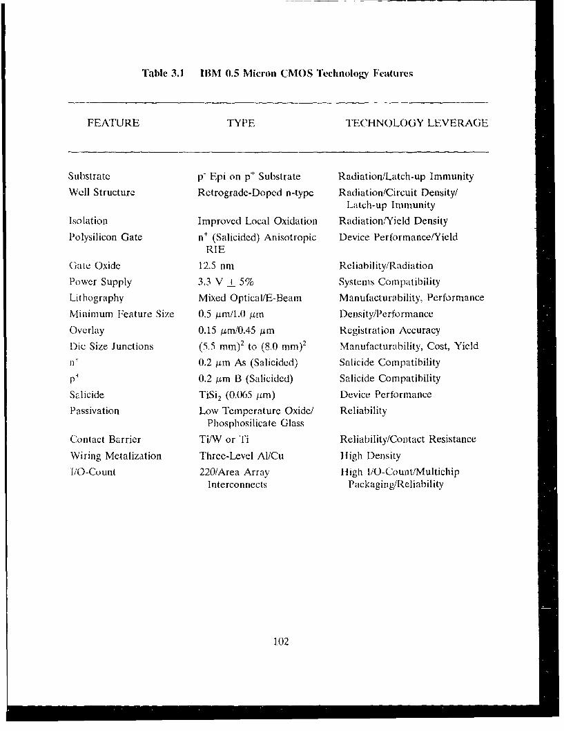
Table 3.1 IBM 0.5 Micron CMOS Technoloao• Features
FEATURE TYPE TECHNOLOGY LEVERAGE
Substrate p- Epi on p+ Substrate Radiation/Latch-up Immunity
Well Structure Retrograde-Doped n-type Radiation/Circuit Density/Latch-up Immunity
Isolation Improved Local Oxidation Radiation/Yield Density
Polysilicon Gate n' (Salicided) Anisotropic Device Performance/YieldRIE
Gate Oxide 12.5 nm Reliability/Radiation
Power Supply 3.3 V A 5% Systems Compatibility
Lithography Mixed Optical/E-Bearn Manufacturability, Performance
Minimum Feature Size 0,5 Am/1.0 Arm Density/Performance
Overlay 0.15 Am/0.45 Aim Registration Accuracy
Dic Size Junctions (5.5 mm) 2 to (8.0 mrm) 2 Manufacturability, Cost, Yield
n* 0.2 Aim As (Salicided) Salicide Compatibility
p+ 0.2 Am B (Salicided) Salicide Compatibility
Salicide TiSi2 (0.065 Aim) Device Performance
Passivation Low Temperature Oxide/ ReliabilityPhosphosilicate Glass
Contact Barrier Ti/W or Ti Reliability/Contact Resistance
Wiring Metalization Three-Level Al/Cu High Density
I/O-Count 220/Area Array Htigh 1/0-Count/MultichipInterconnects Packaging/Reliability
102
CHAPTER 3 / DEVELOPMENT TASKS
Enhanced lIocess: Two levels of radiation hardness were specified in the program; arequired, baseline level and a preferred, enhanced level (see Section 3.3.3). Tests ofdevices fabricated with the baseline process indicated that it exceeded all the radiationrequirement-s and the enhanced requirements for transient upset, survivability, latch-up,znd neutron fluenco. Areas that required improvement in order to meet the enhancedrequirements were identified as total dose and single event upset (SEU).
Total dose enhancement concentrated oii hardening the gate oxide and fieldoxide including the "bird's beak" transition region. This was accomplished by aJlassified process that was independent of the ,hip design and proved successful asdemonstrated by radiation testing. Polysilicon stringers were observed on initial testchips. These were elinminated by modifying the polysilicon RIE etching. The Phase 2chip set was fabricated simultaneously in thle baseline and enhanced processes. Sinceno first order impact on yield, cost, performance, or reliability was detected theenhanced Phase 2 process waý adopted as the primary process.
To facilitate the design of static RAMv (SRAM) cells with SEU protection, aSecond level of polysilicon was used for decoupling resistors and cell wiring in hardenedSRAM designs. The pioccss was tested on 4k x 9 memory arrays.
The performance and radiation hardening specifications were successfully met.Tiwelve split lots of Phase 2 product chirs were successfully processed with both thebascline and enhanced 0.5 micron CMOS process versions. The 0.5 micron devicessurvived 310 Mrad(Si) total dose exposure without any functional failure and with
mnlilirlnal impact to worst case performance.The overall processing flow, vertical device profiles, and other details of the
enhanced process arc given in Reference 3.45.
"The original program plan called for TRW to produce superchips in a 0.5 micron,iadiamion hardened, bipolar technology based on modifying the Phase 1 triply diffused process;Nlotorola wa• to fabricate the same designs in CMOS. The TRW enhancements were toinclude a self-aligned polycmitler, trench isolation, ion implanted arsenic resistors, and triplelevel metal. I lie process required a total of 13 mask levels, all of which would be defined by'-beam,, lithography.
l)uring 1985, "TRWN experienced inconsistent results with the e-beam version of thepoIdn,1ittcl pioccss,. Tihere were also problems with some of the interlayer dielectric materials.Poor device parameters were obtained on test chips and other problems with the triple levelme.tal system appcarcd. Furthermore, delays in delivery of the high throutghput AEBLE-150c-beam inaclhine (see Sect ion 3.3.4) forced the use of low throughput c-beam machines so thatthe slow gathrcling o( cxpcr ircnial tiata slowed the progress of development.
M,'nwlr•ih. M(troj. wa! procoeed-ing with the development of a submicron CMOSproces based initially on Tsing p-/p epitaxial wafers, trench isolation, 150 A gate oxide and
103
CHAPTER 3 / I)EVELOPMENT TASKS
polysilicon gates. Sidewall oxide was to be used for source and drain definition, partialplanarization for first metal, and oxide planarization for second metal.
Early in 1987, a decision was made to discontinue the bipolar effort at TRW and tocontinue developing the CMOS process at Motorola. It was decided to first fabricate allmacrocells to 0.8 micron design rules and then produce a CPUAX superchip (Section 3.4.2)in 0.5 micron geometry.
Motorola also had planned to use e-beam lithography, but when their AEBLE-150machine was finally delivered they found that the overlay accuracy was inadequate. They thenchanged to all optical lithography with a step-and-repeat machine employing a high numericalaperture G-line (later I-line) lens.
The 0.5 micron processing was extremely challenging, especially the lithography whichrequired 135 mask sets for the superchip. The final results were very successful; elevenmacrocells were individually produced in 0.8 micron geometry and two in 0.5 micron geometry.A 0.5 micron BIU chip with 35k active devices and the CPUAX superchip with all themacrocells in 0.5 micron geometry were also produced, the latter containing a total of 4.1million devices. The CPUAX and BIU were successfully demonstrated functioning as aprogrammable signal processor in December 1989.
3.3.3 Radiation Hardening - James J. McGarrity, Harry Diamond Laboratories
The Defense Nuclear Agency (DNA) administered a follow-on effort to the VHSICPhase 1 program (Reference 3.46) that was designed to improve the capability of selectedPhase 1 technologies to meet DoD's requirements for hardness to ionizing radiation in space.These space requirements are:
Neutron fluence .................. 1E12 n/cm 2
Total ionizing dose .............. 2E5 rads(Si)Dose rate/upset ................ . El0 rads(Si)/sDose rate/survivability ............ IE12 rads(Si)/sSingle event upset .............. 1E-10 upsets/bit-dayLatchup .. ...................... none
The work was initiated between 1984 and 1986 via DNA awards to eightcontractor/subcontractor teams. These efforts involved process development and/or circuitdesign, layout, fabrication, and characterization as appropriate to each particular hardeningtask. The areas of concern (luring the program were total dose (TD), (lose rate/upset, latchup(LU), and single-event upset (SEU). The neutron hardness and dose rate/survivability of thePhase 1 technologies were considered to be adequate and were not specifically addressed.
Considerable progress was made in this area by developing new radiation resistantfabrication processes and transistor designs and by implementing innovative, device-levelschemes. The DoD requirements were not only met, but in some cases were exceeded. TheIBM work on Phase 2 radiation hardening is discussed in Section 3.3.2.
104
CHAPTER 3 / DEVELOPMENT TASKS
Westinghouse
A contract was initiated with Westinghouse (prime contractor) and NationalSemiconductor Corporation (NSC) to develop radiation-hardened versions of the 64k SRAMand the 10k gate array which they designed and produced in CMOS during the Phase 1program.
Total dose hardness of the baseline process was limited largely by n-transistor leakagecurrent brought on by positive charge buildup in the field oxide. The approach to hardeningwas to implement a self-aligned field edge (SAFE) implant of boron prior to oxidation toprevent charge inversion and thus cut off source-drain leakage paths. This step was lateraugmented in the gate array with a modest layout revision that recessed the n' source-drainregions away from the "bird's beak" edge of the field oxide. The combination of the SAFEimplant plus the recessed n' yielded a gate array design capable of functioning up to themegarad level (Reference 3.47).
The latchup problem that was experienced initially with the baseline process (Reference3.46) was eliminated by converting to substrates which used epitaxial p layers on p4 as thestarting material.
Motorola
A contract was initiated in FY88 with Motorola to demonstrate a space radiationhardened CMOS 6000 gate array with production to begin in FY89 (Reference 3.48). Thetotal dose hardening approach was to revise the VHSIC baseline process while maintaining85% process flow compatibility with the commercial CMOS process. Motorola modified thegate oxidation process to minimize the oxide charge and interface state contributions to theradiation-induced threshold voltage shift. They optimized the nD doping and implemented agraded drain to improve hot carrier stability at 5 V. Motorola demonstrated a gate oxidewhich resulted in a total n-channel threshold shift of only -0.50 V at 1.00 Mrads. The programwas terminated in FY88 when Motorola announced it was moving its VHSIC technology fromArizona to Texas.
IBM
The objective of the IBM effort was to enhance the total dose and SEU tolerances ofthe 1.25 micron NMOS process. The main total dose hardening effort was directed towardsolving the transistor leakage problem that had limited IBM's Phase 1 "enhanced" process tothe 50 krad level. Additional process enhancements were developed that relied principally onheavier implants in the field and "bird's beak" regions to increase the threshold voltage in theseareas. Transistors incorporating these enhancements exhibited little or no leakage current
105
CHAPTER 3 / I)EVELOPMENT TASKS
increase at 500 krads, and threshold shifts were on the order of 0.5 V at 200 krads. Insubsequent follow-on activities at IBM, circuits were shown to meet the 200 krad spacehardness requirement (Reference 3.49).
A set of radiation environment specifications and goals were established for the baselineprocess. More stringent requirements for radiation hardening were set for the enhancedprocess. The technologies for each requirement were developed as parallel efforts. Theradiation hardening requirements for both baseline and enhanced CMOS device technologiesare given in Table 3-1 of Reference 3.45 which also compares VHSIC Phase 2 radiationrequirements with those for VHSIC Phase 1. The work on radiation hardening during Phase2 is also discussed in Section 3,3.2.
I lu.hes Aircraft Corporation
A comprehensive study was conducted into the effects of SOS starting material on backchannel and edge leakage behavior following irradiation. It was found that back channelleakage could be minimized by the use of Union Carbide type B wafers. Unfortunately,leakage currents remained too high for the CMOS/SOS technology to be considered for highdensity SRAM applications. Evidence obtained during the study indicated that leakage wasoccurring along the bottom edge of the n-transistor sidewall as a result of charge buildup inthe sapphire. Some additional improvements in total dose hardness (circuit functionality toapproximately 5 krads) were realized during the other programs, but the leakage problem wasnever completely ,olvcd (Reference 3.50).
I larris/GE/RCA
At the time of the Phrase 1 program. RCA was the major SOS device supplier in theUnited States and had demonstrated a 3 micron, 16k CMOS/SOS SRAM that was radiationhardened to space levels. Subsequently, a 1.25 micron technology was developed and RCAbecame a second source to Hughes during the Phase 1 program. Because of the interest inhigh density, hardened SRAMs for missile and space applications, a DNA contract wasinitiated with RCA to develop and produce a space-hardened 1.25 micron 64k CMOS/SOSSRAM.
The radiation hardening effort began in 1985 with an examination of means to improvethe hardness of commercial SOS test chips. The major challenge was to harden the basicCMOS/SOS transistor structures to total dose. This involved optimization of processingparameters in order to harden (1) the gate oxide, (2) the mesa edge, and (3) the siliconsapphire interface. Special attention was also given (luring design of the SRAM to furtherimproving its dose rate upset and SEIJ immunities. For example, upset immunity wasincreased in both environments through added memory cell capacitance.
106
CHAPTER 3 / I)EVELOPMENT T1ASKS
Honeywell
Honeywell's Phase 1 bipolar technology proved to be extremely sensitive to single eventupset (Reference 3.46), and a contract was initiated in 1985 to address this shortcoming.
Using the baseline ADB-III process at Honeywell, a family of registers and flip-flopmacrocells hardened to SEU was designed, developed, and tested. Several variations of twocircuit hardening techniques were implemented. These techniques provided SEU immunityby (1) keeping the correct data stored in a dual redundant register or (2) filtering the SEUby adding time delay to the flip-flop's feedback path.
The technique of using a dual redundant latch in place of each single flip-flop elementprovided the greatest SEU immunity (Reference 3.51). By storing data at two independentnodes (gated by Schottky diodes), the scheme permitted fast (1.4 ns - 3.1 ns) registers withlinear energy transfer (LET) thresholds beyond 80 MeV/(mg/cm 2). While doubling the numberof latches doubled the register layout area and power, the demonstrated error rates were lessthan 1E-10 upsets/bit-day. Since registers occupy only a small percentage of most bipolarlayouts, these redundant macrocells can be added to designs with almost no impact onperformance.
The second SEU hardening approach took advantage of the fact that the effect of anSEU strike dissipates within 2 to 380 ns of the event. With this information, flip-flopmacrocells were designed with varying time delay "filter" elements (made from resistors,capacitors, and/or transistors) within the feedback path. This delayed feedback technique wasused to intentionally slow the response time of several latch designs between 1.9 nsec and 30nsec, which demonstrated enhanced LET thresholds between 5 and 38 MeV/(tng/cm 2),respectively. Delayed feedback techniques proved successful where layout area and powerdissipation were most critical but speed could be sacrificed.
TRW
TRW's triple diffused (3D) bipolar technology exhibited latchup during dose ratetesting at about 8E8 rad/s (Reference 3.46). The original solution to this problem involvedenlarging the ground contacts on all n-type resistors. This solution prevents latchup byshunting the base-emitter junction of a parasitic lateral npn transistor in the latchup path, butrequires additional layout area.
The purpose of the DNA hardening effort was to investigate an alternate solution tothe latchup problem by using p- on p÷ epitaxial substrates in a process that is normallyfabricated without an epitaxial layer (Reference 3.52), Device modeling/simulation codes suchas PISCES were used to determine the critical parameters controlling latchup.
107
CHAPTER 3 / DEVELOPMENT TASKS
Texas Instruments
Initial dose rate testing of the Array Control Sequencer (ACS) customization of the 10kgate array chip demonstrated lat-hup on the 2-volt logic supply at approximately 2E8 rads/s(References 3.46 and 3.53). The latchup sensitive areas of this 10k gate array were identifiedby scanning the die using a focused Nd/YAG laser with 150 micron spot size and observingwhether latchup was induced. Infrared imaging of the hot regions revealed two suspectregister file macrocells. Subsequent testing revealed that other customizations of this gatearray which did not use these macrocells were immune to latchup.
Using a CAD workstation, layouts of latching and non-latching cells were compared.Non-latching cells had resistor well contacts spaced at regular intervals. The latching cell hada design error that resulted in only one contact being used in a large n-type epitaxial wellcontaining over 5,000 resistors. Consequently, the well would become debiased in transientradiation environments and trigger a latchup condition. To remedy this problem, twohardening techniques were incorporated: (1) approximately 500 additional contacts were addedto the resistor well; and (2) parts with a single well contact were fabricated using p- on p+epitaxial substrates that incorporated deep trench isolation extending down through the fieldoxide into the heavily doped substrate.
Two-volt latchup was not observed when modified devices were exposed to 1E12 rads/s.The additional contacts eliminated latchup by shunting the base-emitter junction on a parasiticvertical pnp transistor that is foin ed by (he resistor well. For the devices processed on p'substrates, the lower gain of the lateral parasitic npn transistor that is formed between theresistor well and an adjacent collector prevented the regeneration that results in latchup.
3.3.4 Improved Tools and Materials
E-Beam Lithograhy
E-Beam Lithograp[ly Equipment: E-beam lithography equipment with a capacity forhigh wafer throughput was developed to support the fabrication of 0.5 micron featuresize VHSIC chips on a pilot line basis. Hughes/Perkin-Elmer (PE) developed such amachine (the AEBLE-150) under a VHSIC contract which started in 1981 and finishedwith final acceptance test by the Army in February 1985. PE undertook an additional,independent, three year effort to improve the resolution and overlay accuracy in orderto meet the full machine specifications. An AEBLE 150 meeting the requirements wasaccepted by Motorola in September 1988, This successful development provided acapability for e-beam patterning which meets the needs of the U.S. for a machinecapable of moderate production of submicron chips. At the present time, Perkin-Elmer has s( Id approximately 14 AE13LE-150 machines to U.S. and foreign companies.Further improvement of the capabilities of this machine to 0.25 micron resolution isbeiitg undertaken ini a two year contract with the DARPA MIMIC program office. Forfurther details, see References 3.54, 3.55, and 3.56.
108

CHAPTER 3 / DEVELOPMENT TASKS
Perkin-Elmer plans to introduce a 0.5 micron mask maker (MEBES IV) in1991, and to have an enhanced AEBLE-150 capable of fabricating, by direct writing,0.25 micron minimum feature size chips by 1993. A highly accurate 1.25 micron maskmaker is planned for 1994/1995.
Electron Beam Lithography Components: The objective of this VHSIC Phase 3contract with Hughes Aircraft was to develop technologies necessary to build a direct-write e-beam machine capable of meeting the VHSIC Phase 2 goals. Three tasksspecifically addressed were: 1) the development of improved electron-beam columncomponents; 2) the evaluation of a thermal field emitting electron source; and 3) thedevelopment of a very accurate high-speed digital-to-analog converter (DAC).
Hughes developed a unique single lens shaper, the scanning electronics, and the.pattern generator, while Perkin-Elmer designed scanning optics, the final lens, and thebasic LaB 6 e-gun. Hughes was successful not only in developing the DAC, they alsosupplied an extremely accurate 18-bit DAC, a 15-bit DAC, as well as a very fast 13-bit DAC for the electrostatic deflection system. The first 5 AEBLEs built had HuglhsDACs in them. Further details are found in Reference 3.57.
Software for Electron Beam Lithography: The objective of this program by TRW andGCA was to develop the necessary software to operate the GCA e-beam machine,DWM-7000EB. The program called for the development of three versions of software.
Version 0 software consisted of the test programs necessary to support earlyintegration, plus testing of the prototype instrument.
Version 1 software was the minimum software configuration required tosupport basic system functions and test software design and has the followingcharacteristics: 1) emphasis on successful hardware/software integration rather thanthroughput; 2) step-and-repeat stage operation; 3) effect correction and first-orderproximity; and 4) support of non-Manhattan geometries but no support forphotocomposition.
Version 2 software consisted of programs required to support operation of afully-functional production lithography system. This program funded the softwarefunctional specifications.
The goal of this program was to allow GCA to maintain the scheduledavailability of an e-beam machine for the VHSIC Phase 2 submicron phase. Thiseffort was primarily funded to insure the availability of an e-beam machine in the eventthat Ilughes/Perkin-Elmer was unable to develop their e-beam machine in time.
The software program was completed on time and met all of the stated goals.I lowever, GCA shut down the e-beam program in 1984 because of insufficient internalfunds to maintain it. Their c-beam system, DWM 70000EB, was never marketed andthe software technology was never used. See Reference 3.58 for further details.
109
CHAPTER 3 / DEVELOPMENT TASKS
X-Ray Lithography
All of the X-ray lithography programs were awarded under VHSIC Phase 3. Initially,there was a feasibility study program awarded to Perkin-Elme~r. It showed that an X-ray-step-and-repeat lithography was possibl- and had high resolution capability providing the X-ray mask problem could be solved. In 1984, the Government awarded Perkin-Elmer a six yearX-ray development program leading to a submicrometer X-ray step-and-repeat lithographysystem.
Extension of X-Ray Lithography Technology to VHSIC: The objective of this programwith Perkin-Elmer was to develop alignment, work stage, mask, organic resist, andradiation damage free technologies, and to establish performance specifications for ahigh resolution (0.5 micron feature size), high throughput (eight 4-inch wafers/hour)X-ray lithographic machine, Induccd radiation-damage-caused resist exposure wasevaluated, and resist formulations were characterized for exposure properties, dry etchresistance. adhesion, and resolution.
This program was undertaken in support of the VHSIC Phase 2 goals of 0.5micron linewidths. It was intended to establish a high throughput replication techniquefor VHSIC and other submicron circuits, while trying to understand the radiationeffects. This program depended greatly on resist programs, mask technology, and theelectron beam programs for mask making at submicron lincwidths.
The project was completed in December 1981 and produced major enhancementsto X-ray lithography. The success of this program led directly to a program to buildan X-ray step-and-repeat lithography machine which is currently being funded throughDARPA's X-ray lithography initiative.
The program identified alignment sensing techniques for the requiredmask/wafer error of 0.1 micron at 0.5 micron resolution. Titanium and silicon carbidemasks were demonstrated. Several resist formulations were evaluated including drydevelopable resists. X-ray radiation studies showed no adverse effect on CMOS deviceyield, performance, or reliability. Specifications for an X-ray step and repeatlithography machine were developed. X-ray lithography was shown to be a viabletechnique for the high throughput production of submicron integrated circuits. Detailswill be found in References 3.59 and 3.60.
X-ray Lithography Equipment: The objective of this program with Perkin-Elmer wasto develop a lithographic machine capable of patterning submicron chips at highthroughput under moderate production volume. The key features of the X-ray step andrepeat (XSAR) machine specifications and goals for this piogram were: (1) 0.5 micronresolution, (2) 20 wafer levels/hr (with a 10 millijoules/cm 2 resist sensitivity) and fourinch diameter wafcrs, (3) development of a source for the fabrication of high qualitymasks, and (4) installation and testing of the tool in a VI ISIC Phase 2 pilot linc.
Thiq program was undertaken in support of the VHISIC Phase 2 goals of 0,5micron linewidths. It was a direct outgrowth of the "Extension of X-Ray Lithography
110
CHAPTER 3 / D)EVELOPMENT TASKS
Technology to VHSIC' contract and depended greatly on resist programs and theelectron beam programs for mask making at submicron linewidths.
The project was transferred to DARPA in 1989 and is now part of the NationalX-Ray Lithography Institute Initiative. As of January 1990, theie were two fullyoperational XASR machines. One, at Perkin-Elmer has been used by SEMATECHand IBM. The other, at Honeywell, underwent pilot line production testing. Thesemachines are currently for sale.
The program succeeded in building an X-ray step-and-repeat lithographymachine capable of about 15 wafer levels/hr (with a 20 millijoules/cm 2 resist). It alsodeveloped a mask technology capable of producing <0.5 micron linewidths on a boronnitride membrane using gold as the absorber. The machine was demonstrated to theGovernment and the semiconductor industry and one is now installed in a pilot lineenvironment. One other machine at Perkin-Elmer is available for use by interestedparties.
X-Ray J .ith__oraphyvfxpoMure Station: The objectives of this program with Spire, whichstarted in February 1988, were (1) to develop a simple, low cost, X-ray exposure stationfor X-ray resist and mask testing; (2) to develop high sensitivity, high resolution resistsfor X-ray lithography; (3) to test these resists in a pilot line environment, and (4) toprovide a domestic, commercial source for these resists.
This program was undertaken to provide X-ray resists and a means of testingthose resists in support of the VHSIC Phase 2 goals of 0.5 micron linewidths. Itdepends greatly on the electron beam program for making test masks at submicronlinewidths.
The project was transferred to DARPA in 1989 and is now part of the NationalX-Ray Lithography Institute Initiative. As of January 1990, there was one test stationready for acceptance testing, and resists delivered are 10 times more sensitive thanthose on the commercial market. The project was cancelled at this point, with themachine to stay at Spire until a suitable place has been found for it.
The program succeeded in building a low cost X-ray exposure station with thecapability of interchangeable targets. This enabled the machine to simulate X-raysfrom a variety of sources at different wavelengths. Negative resists were developed thatare at least 10 times more sensitive that those on the commercial market. Thisexposure station can be used for testing resists or replicating masks where an alignmentto another level is not needed.
Advanced Wafer Imaging System
The objectives of the VIHSIC sponsored Advanced Wafer Imaging System (AWLS)program were to significantly advance the state-of-the-art technology in optical step-and-repeatlithography. The goal was to develop a produclion prototype rnachiac which could produce
111
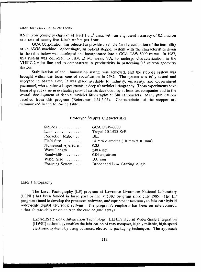
CHAPTER 3 / DEVELOPMENT TASKS
0.5 micron geometry chips of at least 1 cm 2 area, with an alignment accuracy of 0.1 micronat a rate of twenty five 4-inch wafers per hour.
GCA Corporation was selected to provide a vehicle for the evaluation of the feasibilityof an AWlS machine. Accordingly, an optical stepper system with the characteristics givenin the table below was developed and incorporated into a GCA DSW-8000 frame. In 1987,this system was delivered to IBM at Manassas, VA, to undergo characterization in theVHSIC-2 vilot line and to demonstrate its productivity in patterning 0.5 micron geometrydevices.
Stabilization of the illumination system was achieved, and the stepper system wasbrought within the focus control specification in 1987. The system was fully tested andaccepted in March 1988. It was made available to industry, university, and Governmentpcrsonnel, who conducted experiments in deep ultraviolet lithography. These experiments havebeen of great value in evaluating several rcsists developed by at least ten companies and in theoverall development of deep ultraviolet lithography at 248 nanometers. Many publicationsresulted from this program (References 3.61-3.67). Characteristics of the stepper aresummarized in the following table.
Prototype Stcppcr Characteristics
Stepper .......... GCA DSW-8000Lens ............ Tropel 10-1435 KrFReduction Ratio . .. 10:1Field Size ........ 14 mm diameter (10 mm x 10 mm)Numerical Aperture . 0.35Wave Length ..... 248.4 umBandwidth ........ 0.04 angstromWafer Size ....... 100 mmFocusing System ... Broadband Low Grazing Angle
Laser Pantography
The Laser Pantography (LP) program at Lawrence Livermore National Laboratory(LLNL) has been funded in large part by the VHSIC program since July 1985. The LPprogram aimed to develop the processes, software, and equipment necessary to fabricate hybridwafer-scale digital electronic systems. The program's emphasis has been on interconnect,either chip-to-chip or on-chip in the case of gate arrays.
Hybrid Wafer-scale Integration Technology: LLNL's Hybrid Wafer-Scale Integration(HWSI) technology enables the fabrication of very compact, highly reliable, high-speedelectronic systems by using advanced electronic packaging techniques. The approach
112

CHAPTER 3 / DEVELOPMENT TASKS
is that of a "multichip module" in which the interconnection substrate is fabricated ona silicon wafer (a "silicon circuit board," or SiCB). The silicon substrate is a very goodheat conductor and at the same time completely eliminates thermal expansionmismatch between the substrate and the chips. R' a!s,- permits the interconnectionmodule to be fabricated using more or less conventional integrated circuit (IC)fabrication equipment and techniques.
The LLNL metal interconnect is based on "medium film" technology: the metal(typically copper or gold) is about 5 microns thick and 10 microns wide over a groundplane. The pitch is typically 50 microns, which limits the crosstalk to acceptable levels.With this pitch, most complex systems can be routed on only two levels of microstripinterconnect. The fabrication techniques, the signal-propagation characteristics ot thesestructures, and other features of the technology such as on-module resistors aredescribed in Reference 3.68.
There are several techniques that may be used to electronically connect theintegrated circuits to form a functional multichip module. In response to limitationsof conventional bonding techniques, however, LLNL has developed a laser-basedinterconnection technology in which metalization is fabricated directly down the edgesof the chips. This technology coupled with a high quality die attachment, has yieldedextremely high pin-out (e.g., 25 micron pitch, or 1600 interconnections on a single 1cm 2 die). It also has provided low inductance (<0.25 nH per interconnect) andoutstanding heat conduction through the die attachment. The fundamentals of thisinterconnectioa technology are described in References 3.68-3.72. A recorder developedby Fairchild Corp. incorporating a solid state memory that utilizes this technology isnow deployed in a space satellite. A 20-chip memory module on which chips occupyover 80% of the module area has been fabricated with the chip-to-module interconnectwritten on the vertical chip walls.
LLNL SiCB-based HWSI technology has been targeted toward compact, highperformance digital and radio-frequency (rf) systems. Such systems may require liquidcooling. This has been achieved effectively and compactly by the use of microchannelcooling. Microchannel heat sinks can be fabricated directly within a silicon wafer, thusproviding a thermal expansion match to the SiCB. During 1987, LLNL appliedmicrochannel heat sinks to cooling solid-state lasers (Reference 3.73). During 1987through 1989, LLNL applied them to cooling rf power amplifiers, under Air Forcefunding (Reference 3.74).
Laser Direct Write Double Level Metal Technology: An all-dry, double-level metaltechnology for personalization of VLSI gate arrays has been established. The goal isto provide rapid prototyping of new electronic systems, and to serve as the nucleus fora potential job-shop, low-volume manufacturing environment. This resistless, all-drytechnology has numerous potential advantages. The direct-write eliminates theturnaround time for mask fabrication and inspection. The elimination of resist reducesthe number of processing steps and eliminates the need for a class-10 yellow roomenvironment.
113

CHAPTER 3 / DEVELOPMENT TASKS
LLNL has developed all six process modules for this technology: laserdirect-write, metal sputter deposition, metal magnetically enhanced reactive-ion etching(RIE), oxide plasma-enhanced CVD (PECVD), oxide RIE, and Si PECVD.Integration of these modules into a coherent technology has been accomplishedsuccessfully (References 3.68 and 3.75). Using 3-micron lines on 5.5-micron pitch formetal 1 and 4-micron lines on 6.5-micron pitch for metal 2, double-level-metalinterconnect through 100,000 laser-patterned, 2-micron vias has been successfullydemonstrated using this technology. In split runs, LLNL also showed that the yield oflaser patterning is comparable to, or somewhat better than, standard lithography.
LP Laser Equipment and CAD Systems:
LP Hardware: The LP program has developed two types of laser systems, onefor custom VLSI interconnect on flat surfaces, and one for hybrids, wherewriting in the z-dimension is required in addition to x and y. The custom VLSImachine uses acoustooptic (A/O) beam deflection and AKO intensity control toscan a focused argon ion laser beam over a 0.5 mm x 0.5 mm area ("window")of the wafer surface. Precision translation stages move the wafer from windowto window. The focal spot size is 1.0 micron and the positioning accuracy of themachine is 0.5 micron. The hybrid machine rasters the wafer back and forthunder the focused argon ion beam at high speed while an NO modulatorcontrols the intensity. The spot size of the laser on the surface is 5 microns orgreater, dimensions which are appropriate for the purposes of chip-to-chipinterconnect. To permit laser writing on a vertical chip wall, the laser beam isincident on the SiCB plane at 45 degrees.
CAD Systems: The standard means of design entry via a schematic layouteditor has been augmented with a VHDL entry path to allow the capture andsimulation of designs in VHDL format, For more information see Reference3.68.
Advanced Resist Materials and Processes
The objective of this program with H-lewlett Packard was to develop very highperformance electron beam resists. In neg:tive resists, this means a sensitivity of 0.5microcoulomb/cm 2 and a resolution of 0.5 micron lines and spaces. In positive resists, asensitivity of 1.0 microcoulomb/cm 2 is required and a resolution of 1.25 micron lines withvertical walls. Linewidth control must be +/-0.1 micron with dry etch resistance comparableto optical positive resist in CF 4/0 2 and CC14 plasma, and in an argon ion mill. Otherobjectives include wide process tolerance, low pin hole density, resistance to conventional wetetchants, and good adhesion to Si, SiO 2, and Cr.
114
CHAPTER 3 / DEVELOPMENT TASKS
This program was undertaken in support of VHSIC Phase 2 goals of 0.5 micronlinewidths and in direct support of the VttSIC electron beam lithography program. It wasintended to enable the throughput and resolution of the VHSIC and other commercial e-beam resists to be greatly enhanced while providing good dry processing compatibility.
The project was completed in January 1983. The program produced both positive andnegative resists with high sensitivity, good resolution, and high dry etch resistance. Theseinclude a high performance negative resist suitable for high sensitivity (<1 iicrocoulomb/cmn2)and submicron resolution (0.5 micron width <25% linewidth variation). Excellent maskingcapability for dry etching of polysilicon, silicon dioxide, and aluminum under IC processingconditions was demonstrated.
The program also produced two high sensitivity positive resists. One had a sensitivityof 15 microcoulombs/cm2 , resolution <0.5 micron, and fair dry etch resistance. The other wasa silicon containing resist with high oxygen etch resistance useful for multilayer lithography.This resist had a sensitivity of 50 microcoloumbs/cml, <0.5 micron resolution, and excellentdry etch resistance.
Both positive and negative resists were sent to eight VItSIC contractors and the resultswere reviewed. Sensitivity, contrast, resolution, and dry etch resistance were in essentialagreement with Hewlett-Packard data. Joint reviews were also held with Hughes ResearchLaboratory which had a similar resist contract with the Navy. Details are given in References3.76 and 3.77.
3.3.5 Packaging
Introduction
From the start of the VIISIC program it was understood that the packaging andinterconnection of integrated circuits would be critical if they were to operate properly inmilitary systems. A large number of input/output pins would be required in order to interfacethese highly complex devices. This, coupled with the requirement that they operate at highclock speeds, meant that adequate cooling would be necessary to take care of the resultinghigh power dissipation. In addition, the package must allow the ICs to operate under severeenvironmental conditions.
Since no commercial products were available that met these requirements, an extensiveand well-coordinated development effort was undertaken. The packaging/interconnecttechnology had to address such issues as: 1) the fabrication of fine lines on chip substrates,2) the cooling of large chips with high power densities, 3) the construction of multilayer,hybrid substrates, 4) thermal expansion mismatch between dissimilar materials, 5) packagehermiticity, and 6) low impedance leads to support fast rise times and low crosstalk.
In general, the development program was highly successful; the Phase 1 and Phase 2chips were adequately packaged and the state-of-the-art was advanced substantially-Abbreviated descriptions of this effort comprise the remainder of Section 3.3.5. Referencesto reports and contracts are provided for those needing further details.
115

CHAPTER 3 / I)EVELOPMENT TASKS
Feasibility Studies
The earliest efforts to develop the necessary technology were several Phase 3 contractsawarded in 1980 that established the feasibility of various advanced packaging concepts.
"o Honeywell developed the capacity to fabricate fine line contact grids on ceramicsubstrates. Attention was paid to ceramic selection and finishing, and various thinfilm processing techniques were explored (Reference 3.78). This technology becamethe basis for conductor patterning in copper/polyimide thin film multilayers that waseventually used in the Phase 2 program.
"o General Electric demonstrated the technical feasibility of large, complex, high leadcount, thermally and electrically efficient BeO ceramic package fabrication(Reference 3.79). The fabrication process proved difficult, however, resulting in highcost.
" Raytheon developed a methodology for evaluation of device and interconnectperformance using various simulation programs (Reference 3.80). In a separatecontract they also used standard multilayer wafer metalization processes todemonstrate interconnection technology suitable for submicron chips (Reference3.81).
Phase 1 Chip Packages
Single chip packages, both surface mount and pin grid arrays, were developed to housethe Phase 1 chips.
"o The most important features of the packages for the Texas Instruments chip setwere the low impedance signal and ground patterns and thermal pads that ranthrough the bottom of the package, underneath the die attach area (Reference 2.14).
"o A family of three single-chip packages with 42, 161 and 224 I/O pins was developedfor the Westinghouse chips. The package construction was co-fired alumina withperimeter leads on 20 mil centers (Reference 2.15).
"o Honeywell developed three 180-pin array packages on 0.1 inch and 0.05 inch centersand a solder bumped TAB process. New unique features included buried strip lineconstruction and programmable power and ground locations (Reference 2.11).
116

CHAPTER 3 / I)EVELOPMENT TASKS
AdvancedP-ackaMg
The next phase cxtenc -d the VHSIC packaging effort to single chip packages, multichipcarriers, and printed wiring boards to accommodate devices operating at 100 MHz clock rates%Nith greater than 250 terminals. For the most pait, the earlier contracts (1984) came underPhase 3, while the later contracts (1985-1986) were funded by the VHSIC Man(ufacturing)Tech(nology) program (Section 2.2.8).
"o An early Westinghouse contract used computer modeling to determine the mostimportant parameters o" hermetic chip carrier (HCC) - printed wiling board (PWB)systems. Sample HCC-PWB assemblies were fabricated of different materials. Theimportance of closely matching the coefficient of thermal expansion between the1ICC and PWB was confirmed (Referen-e 3.82).
"o I lughcs was the pi contractor for a study to determine the best fabricationapproach for a high (>264) terminal count package with perimeter contacts suitablefor connecting and protecting VHSIC devices. Co-fired ceramic packages producedby Textronix, Inc. offered the greatest ease of manufacture and reproducibility. Thetechnology was developed to produce single and multichip packages as large as 2.5in x 3.0 in with 20-mil and 25-mil pitch leads (Reference 3.83). Since 1985,Textronix has manufactured this type of package.
"o Martin-Marietta and Honeywell undertcok the challenging task of developing highlcaditerminal count, fine pitch packages with high speed electrical performance. A264-terminal, 20-mil pitch, 5-layer ceramic package was successfully designed andfabricated by Martin-Marietta (Reference 3.84) while Honeywell produced a 50-milpin-grid array, 240 1/0 package (References 3.85 and 3.86).
"o A low dielectric constant laminate material for fabrication of printed wiring boardscompatible with alumina leadless chip carrners was developed by I lughes References3.87I and 3.88).
"o Materials and inanufacturing proccsses were devel.ped bT Texas Instruments forhermetic cerainic packages for mountiv,'; and( interconnecting up to nine VHSICchips op,'awing ; tup to 100 MHz and having up to 303 I/O lead... Thin and thickfilm ,ly) iques, as well as tape automated bonding (TAB), were used asintcconuicting schemes (Reference 3.89). Several U.S. sources are available foith(IIIc iriultichip packages.
"o Teledyiie's approar:h to multichip pac'ages wis to develop a co'itrolled impedancestiwsratc. A iow temperature co-fired base with a multilayer thin filin polyimide,nicrosii it) a,;d striplinc signal path was used in order to achl'evc chip communicationat i0(• MHz. See Reference 3.90.
117
CHAPTER 3 / DEVELOPMENT TASKS
"o Low cost, mass production methods for TAB were developed by Honeywell forinterconnection of VHSIC chips to high lead count packages. See Reference 3.91.
" Martin Marietta was the prime contractor on a ManTech program to establishmanufacturing techniques, processes, and controls to produce VHSIC assemblies.Westinghouse was responsible for chip screening and inspection, General Electricwas in charge of the attachment of surface mounted devices to PWBs, and MartinMarietta developed electrical design guidelines to allow PWB designs of desiredimpedance and minimum crosstalk.
"o A ManTech contract with General Ceramics developed first level packaging andinterconnects.
"o A ManTech contract with IBM explored tape (decal) interconnect technology.
"o Third level interconnects were investigated by Sperry.
Testing and Screening
The replacement of aluminum or gold wires for electrical interconnections by polyimidetape and TAB structures introduced a potential reliability problem to microcircuits designedto operate in severe military environments.
o Sonoscan employed acoustic microscopy for non-destructive evaluation of the qualityof metallurgical bonds formed between a tape structure and the chips or substratesbeing interconnected. Good results were obtained (Reference 3.92).
Phase 2 Chip Packages
Each of the three Phase 2 contractors had to overcome challenging problems in orderto design and fabricate packages to house their complex, 0.5 micron devices. Package design,as IC design itself, now required computer aided modeling for the analysis of thermal andelectrical characteristics that was needed to select specific design options.
o 1loneywell designed, built, and demonstrated new single chip and multichippackages. The single chip packages (180- and 269-pin grid arrays) are based on co-fired multilayer ceramic and includes solder reflow TAB for the inner lead bondsand thermocompression outer lead bonds. The multichip package utilizescopper/polyimide fine line, thin film, multilayer intercouinections. See References3.93 and 3.94 for further details.
118
CHAPTER 3 / DEVELOPMENT TASKS
"o The TRW program was divided into two areas: packaging the very large (1.6 in x1.5 in) CPUAX SuperChip (Reference 3.95) and board interconnection. Thespecifications of the CPUAX co-fired alumina package for a cavity flatness of lessthan 0.001 in/in was successfully achieved. In order to limit voltage drops at internalnodes from the high transient currents expected from this complex chip, a uniquepower distribution grid was bonded to the face of the chip and parallel gold ribbonswere welded from the internal package metalization to the grid in several places.The I/O lead count of 308 pins was selected to be compatible with a test socketdeveloped by Texas Instruments (see Advanced Packages section above). Aninnovative, high speed, circuit board interconnection scheme, called "button boards",was developed and tested successfully. It consists of very small "steel-wool-like"buttons that make electrical contact between boards when the board assembly isplaced under compression (Reference 3,96).
"o IBM met all performance, reliability, and environmental objectives for its single chip(SCP) and multichip (MCP) packages. Both packages were attached by IBM's flip-chip, solder ball technique. The SCP is a peripherally leaded gullwing quad flatpack that can be surface mounted to a variety of printed wiring boards. It has 22025-mil pitch I/O leads. The substrate consists of eight ceramic layers. Decouplingcapacitor sites are included on the top surface which permits simultaneous switchingof 64 0.5-micron off-chip drivers across the full military temperature range.Extensive computer modeling, used to determine the thermal resistance of the SCP,facilitated the design of the cooling scheme. The MCP (64 mm x 64 mm) canaccommodate 16 chips and is based on a 42 layer multilayer ceramic substrate. Eachchip can have up to 236 leads. A chip-to-chip data rate of 100 MHz wasdemonstrated. Extensive details are given in Reference 3.97.
119
CHAPTER 3 / DEVELOPMENT TASKS
3.4 Description of VHSIC Chips
At the beginning of Phase 1, the VHSIC contractors undertook to develop, as a group,28 large, complex 1.25 micron silicon chips. They were chosen as demonstration vehicles toperform most of the signal processing functions required in military systems and wert, designedto meet the VHSIC specifications of speed, throughput, feature size, and environmentaloperating conditions. Shortly after the Phase 1 program began, two chips were added to theoriginal 28 and one was dropped leaving a total of 29 deliverable Phase 1 VHSIC chips. InPhase 2, a total of 10 chips of much greater complexity and functionality were originallyselected as demonstration vehicles for design and fabrication at 0.5 micron. Two of the chipswere dropped from the delivery requirements and one was added. These chips are describedbelow. Tables 3.2 and 3.3 list some of the physical and electrical characteristics of all of thedelivered chips. Block diagrams of selected chips have been included to illustrate the varietyof architectural and functional designs that were completed during the program (Figures 3.4through 3.12). Detailed descriptions of the chips from each contractor are contained in thereference listed for that contractor.
3.4.1 Phase I
I loneywell
The chip set (Reference 2.11 and Figure 3.4) consists of a parallel programmableprocessor (PPP), a sequencer, and an arithmetic chip intended for real-time image processing.The primary application is for the computation of enhancement and segmentation functionsused in automatic target acquisition subsystems. An array of up to 32 PPP chips can becontrolled by a single pair of chips (sequencer 4 arithmetic) at a maximum microinstructionrate of 25 MIz. Each PPP chip contains a 16-bit Processing Element (PE) which cancommunicate with its nearest alive neighbor to the left and right. An array of PPP chips hasself-test (originating from the sequencer chip), Dead PPP chips can be identified andbypassed; spare chips can be inserted into the array under the control of the sequencer chip.
PI'P: The PPP chip contains a 16-bit processing element (PE), a 512 x 8-bit PEmemory, a double buffered input I/O memory, a double buffered output I/Omemory, and a control/testing section. The PE can communicate with the left andright neighbor PEs in other PPP chips and can be interrogated by the controllersequencer chip. The PE has a status bit which goes off-chip where it is logicallyOR'd with other PE outputs. The PE has a PE memory associated with it. Theaddress to the PE memory can come from the controller arithmetic chip (globaladdress) or from the PE itself (local address). Each PE has an activity bit whichdisables writing into its own PE memory. A global constant can be transmitted toali ot the l'Ls via the controller architecture.
120
b)Oco 000 00000 0 -T- - ItI 14 r44441-4C1 1 4iNl 1 NNNINzrC'JN 4 -4t
00 ~ O0c) 0c4 4z 'T It 1 o 0N mN lNt I C 40H u r-4
r--r-4
-4 11-4 CNI r-. r- -q- - -4 -4 r-(-4 04C\J 0 C C
1.04) 1- 0 00 ~fr" r - CY 404 0 ii r) <r 4r CO4 r-4 C) C)10C) - r% C)%
a)C C .)r C 0r¼- 000 CC) C1NN4 0LnN-4ut 0 cq 0 W 4C'i0 m D0 0 0000
0 CD 0 1~-410 0- q L %D14ý 0LC %10 U q 1 ONOr-ma n'oC>0 -1 r000004 r)LnC
*.HP4 4CD0 0 0 r- 0 0 0C> nI-4 00o-40o 0 1r- C) O'.000 000> > ý000rnr4 -40C0C % \O'ON D C4 U r )C Nr r tri~0--0 - 4- m4 z N 00 (N U%' ~'t44-1 tm c'j'j m e) m Cl)NqCl)I l n mC4CN f-4 ~ cn Y mm0
"4 000 0. 9 r000 lz 0 0 6 .9( ( 0Zý00 4 0 14C W w 0 0 0 C 00Iid 0 -7 z z z
41 00
4j IQ
ý4 00
V4)
.fr. 'r-4 r-4 r--4 N~' -4 ir 'O4c .f c4 0 Y 0O1
CflO ~ ~ ~ ~ ~ ~ ~ ~ ~ -4c-N t'.-C . tý.4'N-4 ' 0C0A-A4O C(
( 0x
00-ooo 0000000'-40 u
ý4 14 000 0 ý4 0 0 0 000 0
ý4
Li 4-J44.) ý co > -..4m 0 e2 - Jý 4004 14 r-4
,--A41 ) : -4 0 : , -4), -
ý4 4 -uý ', .,-4O0 -i4 0 0 .,4Q w 4) C 4- 4)bO WUU
0 U : 4 r.-Hr (n ýD .- 0) -4 04J -44-Li 4J 0(/ r. Dbo4) 1- z -. 4.0 CO ý4 41 j4-'-
P6 , -4) U~ 0- UD- ý4) CD X D ý 0 >to - o ia u Eý :5 u 2c41 0 w f5 ~ >ýr=
-4 r.4. r c -4 0 LiM( 0 CV4 4)4V4 ~ 0 V) )W >4JCo 0 D ., r4)--4 4) (ni~ -4) 4-4 -4d na J: 4-4C E 4 4 10 Eci, UH m z4 4 (n Z. 0 ) 0 > 4 0 C 4-4 Q) " -4 0 1 4 ) (JL. r4) 0 a U-r4 --4 -4 ri 04
4) (L) 4 .. 0 : (V4) 1 W " Z 0 d 4 : 4) 44J4 4 '1 ý"4 < 34)zv~/ u Q) A 4 r '.CQ-441:, mP--4 F-I0 <ý 0 " J r V) 4 4. a) 0ii
0o 000 00000 fLnr-4lCN mlw N .10 0 0-14 r-- r- oo co 00 co a 0 r~ - en r'- r-Iq w r- r, vi 0 cN4
H 0 1 CNC -14-4 -I r-4 4-1 %4 r-4 1-4 r-i -1v-4
0o Lfl r-4N-It - C7%It0000ONcn r-CO 14 c-CNC'J3Cf 0'¼ M~ en O-t Lfc-C14 JLnNC
000 m tflCfl 0frU 0r-4 0CJ CD0 0N0 0r0
'e4ly r 0 -- 4 4-4
0000-1 tftftl-lv- O 0C'J00r4N-Lf
t ýý 00 00 %D0 000 0 00 0Z Z ZZZ v-IZZZ ZZ'ZZ
00
-I' - 4 CO C41 0 ca w
Ir t7 0'4 N-' n m'I U-1 fD 0) 4)4J 0
-4-40 w
ý4 00)
co a-C ada
r -r4 -H- U -It---4 0I 0
C*4~L 0 ý
rr 4.00)0 0 0 0 00 '40
u 04-4 0.
Ci v-0
O4 0000 0- 0-I zoo0 00 -4"
0~~~~- -45'4 U )~-
a) 1-4 r-4 0UW 4co
-4 4 r- 04J$)'b -'4$0)00Z $0C1 0o c C Co 4)j u ) - wJ
LI4i 0~-t)' Q~ i -4 U 0 U04 Q 6
-0 0 C-.)C0 ~ 0 r- UC W 0 jý .r-0U 4-) C-v00
t4-) Of--x b " r0-IWN Cd )
0 -0 4- $-J $ OflWJ4-40ý W0 Cr4 $x Cl.
wo "-Oj- 4.4 tI2 -) - :::) UWo C-i- 4C a r (btiit CW< DW~ 0r F ýC04)(
I-I) Q'.'->a)-CA0c a)a)I-w4 -00 -i 2 1 -4
4) ac) WCH'q , tu ibD C ~ '-Ir-4 O'dE 5:3-40
v- U 4 4 r-I L 4 ) 4 4 - 2
00p COU 4 4 P 40 ru (4C 4 () p C)p : L 1ug0ý a w .4: O J E . )Vz DV :- )>
9
z :
----
0-
(flL mw Iw I
s0 0I~.010 La
L --
200
i~FW1ia0
'34 .0-
CL 0 QUo(
CHAPTER 3 / DEVELOPMENT TASKS
Sequencer: The main function of the sequencer chip is to generate high-speed (25MHz) control signals for the PPP and arithmetic chips. The sequencer is amicrocode-sequenced machine, with a 1024 x 80 bit ROM on chip. The chip iscapable of issuing a PPP control and address instruction every sequencer microcycle.The sequencer chip has a PPP chip test, an arithmetic chip test, and a self-testsection. It also has an external RAM/ROM interface for microcode expansion, tobypass the internal microcode ROM during debug and checkout.
Arithmetic: The arithmetic chip has two arithmetic logic units (ALU), a specialaddress generator, and a bus interface section. The primary function of thearithmetic chip is to generate addresses at high speed (25 MHz) for the PPP chips.The arithmetic chip is a microcode-sequenced machine, with a 512 x 80 bitmicrocode ROM on chip. A PPP control and address instruction can be issuedevery arithmetic chip microcycle. Additional hardware automatically addresses aPE's own or neighbor memories.
The arithmetic chip has a self-test section. It also has an external RAM/ROMinterface, for microcode expansion, to bypass the internal microcode ROM duringdebug and checkout. The arithmetic chip can support two bus interfaces: a globalbus for communicating with a higher level processor and a local bus for externaldata RAM usage.
Hughes
Hughes selected three key signal processing functions which are generic to anti-jamspread spectrum communication applications and designed each of the functions into aseparate chip (Reference 2.12). Each chip is programmable through electronic reconfigurationof its internal cell interconnections to provide a wide range of system applications. Analgebraic coder/decoder chip, which was designed early in the Phase 1 program, was replacedby the multichannel correlator described below.
Multichannel Digital Correlator: This chip performs matched filter detection of longcoded preambles in which phase coherence is achievable over at least a portion ofthe preamble. Each chip is composed of four identical 32-stage, 4-bit, parallelcorrelator sections integrated into one 128-stage chip in a highly regular array. Bycascading multiple chips, correlators up to 10,912 stages long may be built. For fastfrequency hop applications, multiple input channels are provided for receiversoperating over portions of the frequency band.
Sinle-ChannelDiital Correlator: (Figure 3.5) The single-channel digital correlatorperforms the same matched filter detection of long coded preambles but the logicfunctions which provide independent input channels in the multichannel digital
124
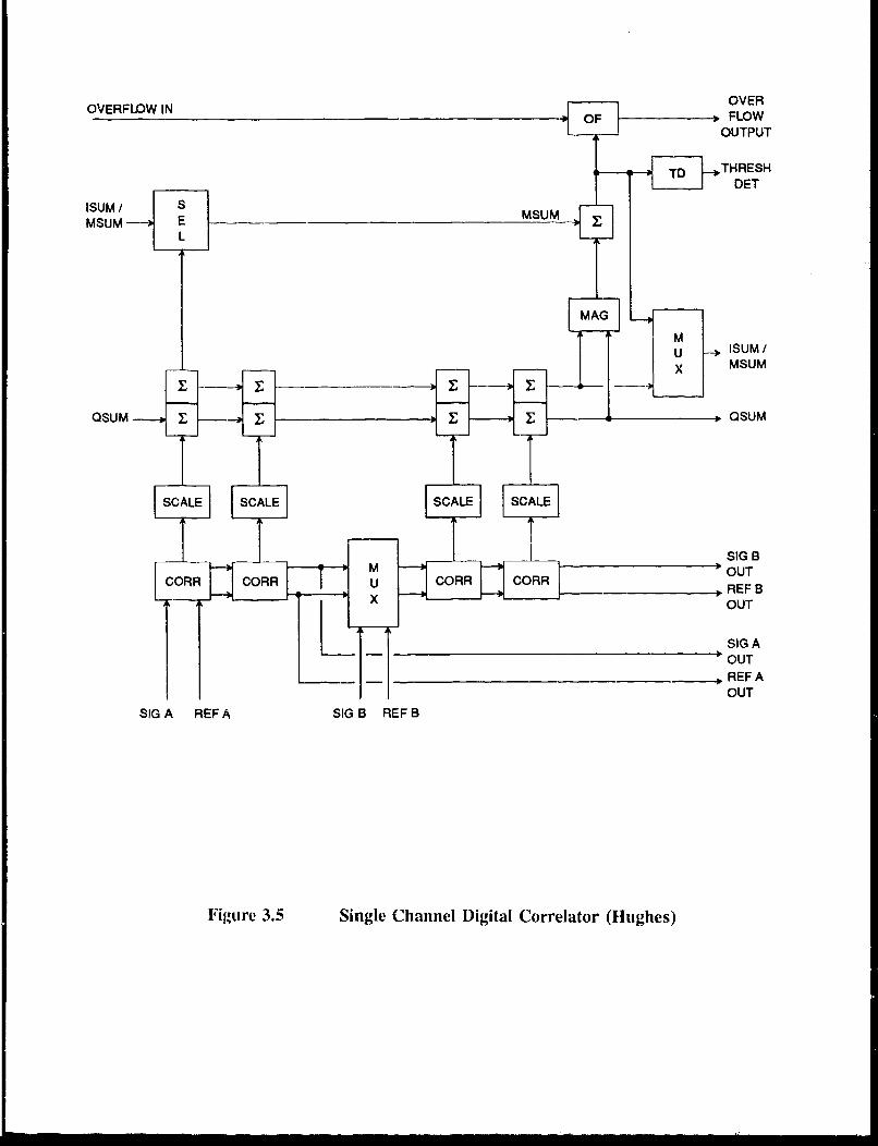
OVERFLOW IN OVEROV47W1F FLOW
OUTPUT
TD THRESH
DET
MSum EL
MAM
u ISUM/MSUM
SCALE SCALESCL
SIG B
CORR CORR U CORR CORR
OUT
SIG A• OUT
SREF AOUT
SIGA REFA SIGB REFB
Figure 3.5 Single Channel Digital Correlator (Hughes)
CHAPTER 3 / DEVELOPMENT TASKS
correlator have been eliminated. Each of the four sections is independentlycontrollable over a bus from an external control processor.
Signal Tracking Subsystem: The STS chip provides tracking and data detectionfunctions. The chip contains a programmable pseudo-noise (PN) pattern generator.Three types of digital tracking loops are implemented on the chip. These providePN code tracking and data demodulation and carrier phase or frequency tracking.
IBM
IBM designed a single chip tailored to the digital processing required in the front endof sensor systems such as sonar surveillance for which the signal processing demands areextremely high (Reference 2.13). Flexibility for use in a variety of such systems under differentconditions is obtained by using an initialization parameter to select from among a set of sixalgorithms that have been implemented in the chip. For acoustic signal applications thealgorithms include: finite impulse response (FIR) filtering, real and complex; real halfbandFIR filter with quarter band shift; beamforming; complex band shift; and discrete Fouriertransform.
Complex Multiplier/Accumulator (CMAC): (Figure 3.6) The CMAC is a parameter-selectable signal processor that can perform 100 million multiply and accumulatefunctions per second (with a 25 MHz clock). The high performance is achieved witha simple data flow that uses four subsections connected in a linear array. Eachsubsection contains a multiplier and adder which can be configured to execute realor complex multiplication and addition.
The chip also contains fault tolerant and self test features with monitoring andreconfiguration capabilities. A simplified version of this chip using only one of thearithmetic sections was designed and built. This signal processing element (SPE)chip became a part of Phase 2 of VHSIC and is described below.
Texas Instruments
Texas Instruments developed a set of eight ICs for military data processing and signalprocessing applications (Reference 2.14). The MIL-STD-1750A instruction set architecture(ISA) was selected for the data processor. An array processor optimized for 16-bit integerarithmetic was selected for the signal processor.
Data Processor Chip Family:
Data Processor Unit: (Figure 3.7) The DPUI is a general purpose microprocessorwhich implements the MIL-STD-1750A instruction set with extended precision
126
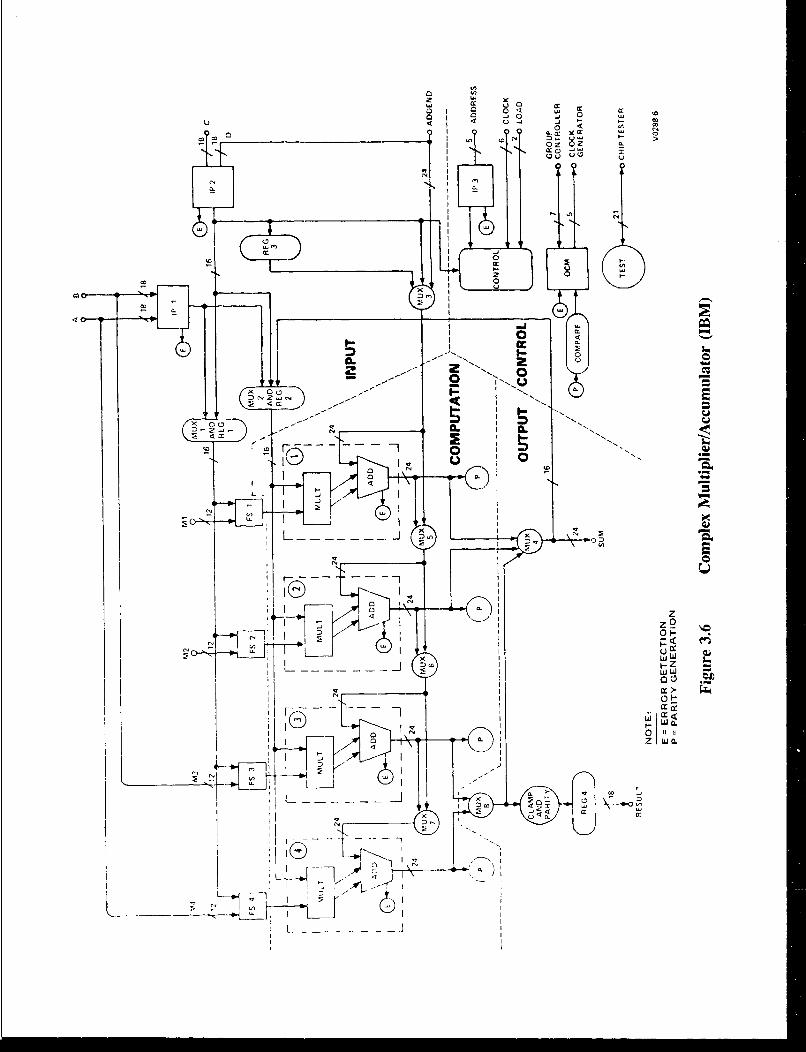
00
co D
LI 4-
x2
LAW i..
IS-
Z w m
CDDj Icc

M-BUS DATA ADDRES
Ki
J n,"- b, i: La -
< -INTERRUPTS
I ---
SIR• IAE IHF kII
BARE SHIFT
'gre 37 DMSR
i iX -BAR L _ ,i
RFO RFF" MI/MC
Figure 3.7 Data Process•or U~nit (Texas Instruments)
CHAPTER 3 / DEVELOPMENT TASKS
instructions. A pipelined architecture provides multilevel instruction look ahead and a 32-bitarithmetic path. The processor carries out all MIL-STD-1750A instructions including floatingpoint, and provides the interfaces required to support interrupt structures, memory extension,and I/O command structures defined in the standard. Four memory addressing methods aresupported by the DPU.
Device Interface Unit: The DIU provides interchip communications support for themultiprocessor with direct memory access, programmable I/O control, and operatingsystem kernels. The chip is similar in structure to the DPI.J. Features unique tothe DIU are provided in microcode.
General Buffer Unit: The GBU is a bus coupler between a memory bus and a systembus. It provides three methods for accessing the system bus: vying for the bustransmission, reception of message headers, and transmission of bus data.
Array Processor Chip Family:
Vector Arithmetic/Logic Unit: The VALU is a reconfigurable, 16-bit arithmeticpipeline with limited floating point operation and multiple precision. It is capableof 25-75 MOPS. The VALU includes a sequencer that generates 13-bit addressesfor addressing external microinstruction memory.
Vector Address Generator: The VAG generates two dimensional array addresses witha full function ALU, concurrent I/O support, and self-sequencing capability.
Array Controller/Sequencer: The ACS is a general purpose microprogram sequencerwhich provides addresses for external or internal memory. The ACS also handlesstarting and stopping of the array processor during reset and maintenanceoperations.
Multipath Switch: The MPS is a 6 x 6 crossbar switch, 4-bit slice deep. The number,direction, and arrangement of the paths can be changed each clock cycle. The chipalso contains a maintenance bus interface and conti.Iller to perform on-chip selftesting.
Memory Chip:
Static Random wccess Memory: The SRAM is read/write memory in an 8k x 9 bitarray organization with on-chip parity checking and lk block write protection. Ithas an internal register for pipeline operation and a reset function to return theSRAM to a known state.
129
CHAPTER 3 / DEVELOPMENT TASKS
TRW
TRW specialized the design of its chip set for high signal throughput electronic warfare(EW) applications but with sufficient flexibility to be useful in a wider range of signalprocessing systems (Reference 3.98).
Window Addressable Memory: (Figure 3.8) This specialized chip provides front-endsignal sorting based on data falling between stored upper and lower limits iiimultiple dimensions. It uses eight 48-bit windows each with up to 12 fields(dimensions) that can be loaded under program control. An incoming 48-bit wordcan be simultaneously tested for inclusion in the windows. An indication is providedif inclusion occurs and a register specifies within which window or windows it wasincluded.
Content Addressable Memory: This chip also provides high speed sorting capabilitybased on data exactly matching stored words. It has thirty-two 48-bit memory cellson each chip that can be loaded under program control. An incoming 48-bit wordcan then be tested for a match with any memory word. Bit masking permits thecomparison to ignore certain bits. A flag and match identifier are output.
Register Arithmetic Logic Unit: Arithmetic and boolean functions ale implementedin a 16-bit word format. The chip can perform double precision computation ormay be cascaded to implement a multi-chip RALU. A 16-bit x 32-word, 3-portRAM provides scratch pad memory.
Multiply/Accumulate: This chip computes sums of products, accumulates intermediatedata, and outputs results for such functions as dot products, matrix multiplies, andFFTs. Instructions control the loading of the input, output, and internal registersas well as reading from and writing into the RAM.
Address Generator: The AG generates a 16-bit address each clock cycle for fetchingand storing data words. Once set up, an AG will generate sequences of addresseswith minimal control, including stopping or auto-restoring on completion.Operations involve up to 6 registers which are held in separate RAM files. Anentire bank of 6 registers can be easily substituted for another to aid in contextswitching.
Microcontroller: The MC generates program addresses for fetching program controlwords. Address generation can be absolute or conditional, direct or offset.
Matrix Switch: The MS consists of an 8 x 8 crossbar switch, four bits deep to providehigh speed data line switching. Each of the eight output ports can be configured
130
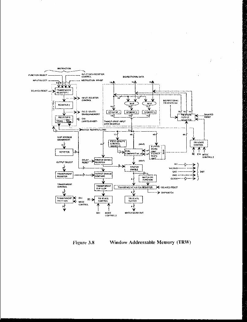
C,0,NTFCL *DIRECIONAL (ATA
DZIAY2) REhT -RRPS7'
REGISTE IEST
CO4*TROk OI fR IONAL(EISF Z AX & TRI STATF o
FVrLENGT 1 ITLZIt_. _1 lT
REaI-iP f(JES 8i
(WRITE f TRITATM
L T L..............-.- - ' T 'CIIIPG.DDES 4, 481, 45,
TAO I .TO
EGISTER~6 ENTUTNIJE wL,.] 7F
TRARSPAW(EN2
OVTPVPREN SEEC RESETJ'~N MRCH9OIE <-flA'E AE
E ARIF rOD .JATH WORD OUT
O(M ~ ~ ~ ~ ~ ~ C(JROL 2AAPRN n WNMXR0GE
F'i FLIP 3.8 P Window AdrssbeMeoy TW
C.IAPTER 3 / DEVELOPMENT TASKS
to select any of the eight input ports. The switching state may be changed eachclock cycle or set and left in any combination.
Four Port Memory: This chip has a 1024-word by 4-bit CMOS memory capable ofreading two independent addresses and writing into another two independentaddresses each clock cycle. Chip select address extension permits combining chipsfor up to 64k words of memory. It may be operated in a pipeline, synchronous, orasynchronous mode.
We.,•tinghouse (Reference 2.15)
Pipeline Arithmetic Unit: (Figure 3.9) The pipelined arithmetic unit (PLAU) is ageneral purpose, programmable, 40-MHz chip vector signal processor. The PLAUsupports logical, real, and complex operations in addition to integer and fixed pointfunctions. The PLAU can also be organized in a variety of pipelined configurationsand can be used in pairs to perform high speed complex computation.
Extended Airltinietic Unit: The extended arithmetic unit (EAU) is an arithmeticcomputing chip which can be combined with the general purpose controller,memories, and gate arrays to form a microcomputer which executes the MIL-STD-1750A instruction set. The major functional sections of the EAU are I/O,multiplier, 32-bit floating point ALU, 16-bit fixed point ALU, RAM, microcodecommand register, and built-in-test circuitry.
Extended Arithmetic Unit Multiplier: The 32-bit extended arithmetic unit multiplier(EAUM) chip provides high-speed, fixed and floating point multiply/divideoperations. It supports the 1750A format and is optimized for 32-bit operations ata 25-MHz clock rate.
General Purpose Controller: The GPC is designed for use as the microprogrammedcontrol element in embedded 1750A and 1750 GP computers. The GPC can directlyaddress 256k of memory and has instruction fetch overlap capability. A built-in testcapability also resides on the chip and can be used at the wafer, component, andmodule levels.
10k Gate Array: The gate array provides specialized support functions for the customchips and the 64k SRAM. These functions include random control logic, interfaces,crossbar switching, barrel shifting, memory address generation, and clockdistribution. The chip has 11.3k gates implemented as a routable array of 7904 cellssurrounded by 152 1/0 buffer cells. The chip is personalized with the help of aminicell library which contains approximately 60 standard logic functions.Approximately 20 percent of the gate count is dedicated to built in test.
132
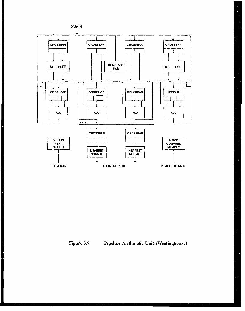
DATA IN
CROSSBAR CROSSBAR CROSSBAR CROSSBAR
MULTIPLIER CSTAMULTIPLIER
CRSSBAR CROSSBAR CROSSBAR CROSSBAR
I 1 _ I IRSSA
ALU ALU MALU ALU
CROSSBAR
BUILT IN MICRO"rEST COMMAND
CIRCUIT MEMORY
NO RMAL N R A
TEST BUS DATA OUTPUTS INSTRUCTIONS IN
Figure 3.9 Pipeline Arithmetic Unit (Westinghouse)
LM_
CHAPTER 3 / DEVELOPMENT TASKS
Static RAM: The 64 kbit SRAM has separate pass/latch control inputs for the on-chip input and output registers. Four modes of operation are possible: (1) fullyasynchronous; (2) asynchronous input and synchronous output; (3) synchronousinput and asynchronous output; and (4) fully synchronous mode for pipelinedoperation. The design of the 64k SRAM uses column redundancy to enhance theyield.
3.4.2 Phase 2
Honeywell
Honeywell chose to design its Phase 2 brassboard chip set (Reference 3.99) using twogeneric bipolar CML gate arrays --- a 35,000 gate array for the B3U chip and a 70,000 gatearray for an array processor and an array controller. The larger gate array is also configurablein the sense that custom macrocells may be substituted for any of the six sectors of the gatearray. The brassboard chips were then designed as personalizations of the basic gate array byappropriately routing the upper metalization layers.
Array Processor Unit (APU): (Figure 3.10) This chip performs the basic arithmeticcomputation optimized for electrooptical image processing. It is similar infunction to the PPP chip of Phase 1 described above.
Array Processor Controller (APC: This chip provides the control functions for theAPU and memory chips which constitute a logical processor module.
Bus Interface Unit (BIU): The BIU provides a data interface between a standardbackplane PI-bus and a Functional Interface Unit chip which then communicateswith the rest of the chips in a board. The board side of the BIU is a directmemory address interface with multiple block and block skip addressingcapability.
IBM
The IBM chip set was designed for general purpose, high speed, digital processing withspecific application to the iiceds of sonar systems (Reference 3.45).
Sfsytolic Processor .()': (Figure 3.11) The SP chip contains a dual 16-bit multiply/32-bit ALU and featu,.s a high speed partial product adder funtioning at 100 MI-1z.The SP is pipelined iiternally to maintain a high throughput rate. The twomultipliers can be used together to perform complex arithmetic or to perform Itwo-point, real arithmetic.
134
I I

U,
CL a.o Gc o c
0<<
x --
1 0 < < o a oO u c rr CC c 0 <0
w a) co
occ
cc LL.. W _
-x
co
S_..-
C*
< 0"0 Q.0
o w
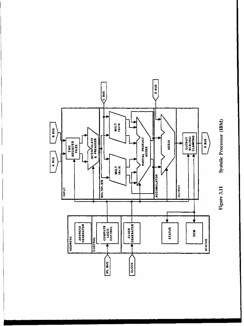
LID,
LUU
01-0 J
00
UA,
I-.
a --
w ,zo-
CHAPTER 3 / DEVELOPMENT TASKS
Configurable Static Ram (CSR): This 18-kbit static RAM provides a complete memorysubsystem on a chip. It has four independent 256 x 18-bit memories which canbe reconfigured electronically to into a variety of 18-bit and 36-bit wideorganizations. The CSR chip provides this reconfigurable structure through theuse of two 18-bit input ports, two 18-bit output ports, and two address ports.
Address Generator (AG): The AG chip generates memory addresses for the CSR andalso generates address sequences for use in digital processing. It has twoprogrammable 16-bit address generators and a 12-bit address counter withprogrammable start and stop addresses.
Bus Interface Unit (BTU): The BIU provides an interface between a standardbackplane PI-bus and the rest of the chips in a board. The board side of theBIU is a direct memory address interface with multiple block and block skipaddressing capability. The BIU can be used to write and read data of controlmemory, to verify memory integrity through the read capability of the directmemory address, or for initial program loading of discrete registers into chips.
Signal Processing Element (SPE): The SPE performs multiply and accumulatealgorithms. It consists of a single computational subsection similar to those inthe CMAC chip described above and performs the same algorithms.
TRW
The TRW/Motorola team developed a unique design and fabrication methodologycapable of producing "superchips" whose size (1.5 in x 1.6 in), number of transistors, andfunctionality were up to two orders of magnitude greater than current state-of-the-artintegrated circuits (Reference 3.100). To accomplish this, the superchip is comprised of blockscalled "macrocells", each equal to or greater in complexity and size than VHSIC Phase 1 chips.Different macrocell types are interconnected on one chip to achieve the functionality of thesuperchip. In order to attain overall yields of greater than 10%, a sufficient number of sparesof each type must be provided to achieve a working superchip. Built-in test circuitryautomatically checks the functionality of each macrocell and reconfigures their interconnectionsas needed. Triply redundant busses are used on the chip to ensure reliable connectionsbetween the various macrocells and I/O ports.
Two large area, 0.5 micron chips with high functional complexity ("superchips") wereoriginally begun in Phase 2 in addition to a BIlU chip. The superchips included a signalprocessor (in CMOS at Motorola and a convolver in bipolar at TRW). These superchips weredesigned but not built because the processing technology could not project a sufficiently highyield to make their successful fabrication likely. Instead the CPUAX, which consisted of the
137
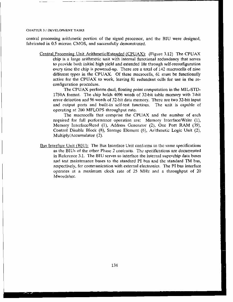
CHAPTER 3 / DEVELOPMENT TASKS
central processing arithmetic portion of the signal processor, and the BIU were designed,fabricated in 0.5 micron CMOS, and successfully demonstrated.
Central Processing Unit Arithmetic/Extended (CPUAX): (Figure 3.12) The CPUAXchip is a large arithmetic unit with internal functional redundancy that servesto provide both initial high yield and extended life through self-reconfigurationevery time the chip is powered-up. There are a total of 142 macrocells of ninedifferent types in the CPUAX. Of these macrocells, 61 must be functionallyactive for the CPUAX to work, leaving 81 redundant cells for use in the re-configuration procedure.
The CPUAX performs dual, floating point computation in the MIL-STD-1750A format. The chip holds 4096 words of 32-bit table memory with 7-biterror detection and 96 words of 32-bit data memory. There are two 32-bit inputand output ports and built-in self-test functions. The unit is capable ofoperating at 200 MFLOPS throughput rate.
The macrocells that comprise the CPUAX and the number of eachrequired for full performance operation are: Memory Interface/Write (1),Memory Interface/Read (1), Address Generator (2), One Port RAM (39),Control Disable Block (8), Storage Element (6), Arithmetic Logic Unit (2),Multiply/Accumulator (2).
Bus Interface Unit (BIU): The Bus Interface Unit conforms to the same specificationsas the BIUs of the other Phase 2 contracts. The specifications are documentedin Reference 3.1. The BIU serves to interface the internal superchip data busesand test maintenance buses to the standard PI bus and the standard TM bus,respectively, for communication with external electronics. The PI bus interfaceoperates at a maximum clock rate of 25 MHz and a throughput of 20Mwords/sec.
138
Table Memory (4k x 39)Write
MINT1W 1PRAM AGTable (3/1) (88/39) (3/1) AG Control
Memory -&,- go 0 DataLoad CDB Read Memory
Data
Tonstants
MITI (11/8 AG/6
AUMAC 1(7/2)(6/2)
I I-
Note: (# of macrocells in macroset / # of macrocells required)
Figure 3.12 Central Processing Unit, Arithmetic Extended (TRW)
CHAPTER 4 - BRASSBOARD DEMONSTRATIONS
4.1 Phase 1 .................................................... 1424.i.1 Electiooptic Signal Processor (EOSP) - Honeywell ............... 1424.1.2 Enhanced Position Location Reporting System (EPLRS) - Hughes .... 1434.1.3 Acoustic Signal Processor - IBM ............................. 1434.1.4 Multimode Fire and Forget Missile - Texas Instruments ............ 1444.1.5 Electronic Warfare Demonstrations - TRW ..................... 1444.1.6 SRAM, Gate Array, Arithmetic Unit, and an ATF Complex Vector
Processor - W estinghouse . .................................. 145
4.2 Phase 2 ..................................................... 1454.2.1 Acoustic Beamformer Module - IBM ......................... 14f4.2.2 Cruise Missile Advanced Guidance - Honeywell .................. 1454.2.3 Demonstration Module - TRW .............................. 145
141
CHAPTER 4
BRASSBOARD DEMONSTRATIONS
The products that resulted from the development tasks carried out by the contractorsduring Phases 1, 2, and 3 of the VHSIC program were tested, evaluated, and demonstratedin a variety of ways. The Phase 1 and Phase 2 contracts called for the demonstration ofVHSIC chips in brassboards which performed a useful system function --- such as high speedsorting of signals in electronic warfare receivers, or coding/decoding of secure communicationchannels. In most cases, the brassboard was designed to demonstrate a specialized functionof a particular class of military equipment. In a few cases, the brassboard demonstrated ageneric algorithm such as the Fast Fourier Transform which is widely used in signal processingapplications.
In addition to the brassboard demonstrations described in this chapter, a substantialeffort at Army, Navy, and Air Force facilities went into the test and evaluation of individualchip types delivered to the Services under the contracts. This activity is discussed in Section3.2.1.
Finally, the VHDL and other software tools developed under VHSIC have beendemonstrated through extensive use in many p1ojects in ordei to improve the efficiency of thedesign process and to document the hardware design data. VHDL_ and supporting softwaretools allow the performance of a system to be analyzed through modeling and simulation.Modeling allows the designer to capture, refine, and verify the properties of the system at alllevels of design. When the model can be simulated, then the behavior of the system in variousdynamic states can be observed. Some of these software demonstration projects are discussedin Section 5.6.
4.1 Phase 1
4.1.1 Electrooptic Signal Processor (EOSP) - Honeywell
Honeywell designed its Phase 1 chips and demonstration brassboard for use in theprocessing of electrooptical image signals. The final demonstration of the brassboard wasconducted for a tri-Service review team on September 17, 1985. Coirect operation of theEOSP chip set was successfully demonstrated while performing two different image processingalgorithms in near real-time. The capabilities of the chip set to perform self-test and toperform dynamic reconfiguration for fault tolerance were also successfully demonstrated.
The focal point of the brassboard demonstration was the segmentation algorithm.Microcode for the low-level computational primitives, which support both the execution of thealgorithm and the fault tolerance functions, was generated and stored in the on-chip ROMsof the sequencer and arithmetic chips. These primitives were sufficient to demonstrate theimage segmentation algorithm as well as seveial uthlii general purpose signal and imageprocessing algorithms.
142
CHAPTER 4 / BRASSBOAR1D DEMONSTRATIONS
Three manuals were prepared for delivery to the Air Force VHSIC Program Office.The "VHSIC EOSP User Manual" provides information to future users of the EOSP chip set.The tools utilized. the design methodology, and applications information is also provided. The"VHSIC Brassboard Development System Reference Manual" contains an operationaldescription of the hardware and software developed under the VHSIC Phase 1 developmentprogram in support of the EOSP brasssboard development and demonstration. It can be usedto operate and maintain the system. The "VHSIC EOSP Brassboard Reference Manual"provides descriptions of the brassboard hardware and firmware developed specifically to house,interconnect, and operate the Honeywell EOSP chip set for the purposes of test anddemonstration. See Reference 2.11.
4.1.2 Enhanced Position Location Reporting System (EPLRS) - Hughes
The manpack user unit of the Army EPLRS (formally identified as the PLRS JTIDSHybrid system) was the vehicle for brassboard demonstration of the Hughes VIISIC anti-jamcommunication chipset. The primary objectives were: (1) to demonstrate the performancecapabilities of the three chip types to the greatest extent practical for this application and (2)to evaluate the potential benefits of the chip set for that system. The versatility of the chipswas demonstrated by implementation of six new higher performance waveform modes in thebrassboard unit and in a companion Demonstration Driver Unit. By capitalizing on themicroprocessor controlled reconfigurability of each member of the chip set, a relatively simpletechnique for dynamically "programming" the signal processing parameters used by each chipwas also demonstrated. The demonstration was successfully conducted at Hughes in late 1986.See References 4.1 and 4.2. Further activity in the insertion of VHSIC into the EPLRS isdescribed in Section 5.1 (Army Insertions).
4.1.3 Acoustic Signal Processor - IBM
IBM successfully demonstrated its Phase 1 Complex Multiply and Accumulate (CMAC)chip in an acoustic signal processing brassboard on May 1, 1984. This demonstration verifiedthe ability of the CMAC to carry out high speed signal preprocessor functions in Navy anti-submarine warfare equipment.
For example, the Navy's P3-C ASW aircraft processes and analyzes acoustic data fromocean sensors (sonobuoys) in the AN/UYS-1 Advanced Signal Processor (ASP). The datafrom each sonobuoy is demultiplexed by the Input Signal Conditioner (ISC) of the ASP intothree separate data channels. These data channels are then analyzed by the ASP ArithmeticProcessor (AP) to provide target detection and bearing information. The brassboard containedfour VHSIC CMAC chips configured as a digital, high throughput replacement for theprimarily analog ISC in the AN/UYS-1. It also contained an Availability ManagementSubsystem that monitored the status of the four CMAC chips and demonstrated all of thebuilt-in-test and fault tolerant features of the CMAC. The brassboard subsystem was designed
143
CHAPTER 4 / BRASSBOARD DEMONSTRATIONS
as a plug-in, connector-compatible replacement for the ISC which would double the numberof sonobuoys that could be processed by the ASP. No haidware modifications to the ANFUYS-1 were necessary.
The VHSIC brassboard not only demonstrated the VHSIC technology, design tools,and CMAC chip performance but also the high speed control concepts that were developedfor the CMAC signal processing. It provided a baseline example for future technologyinsertion into the front end of acoustic signal processors. See Reference ""3.
4.1.4 Multimode Fire and Forget Missile - Texas Instruments
The Texas Instruments Phase 1 demonstration brassboard was originally defined tosupport the Multimode Fire and Forget (M 2F 2) missile. During the program, the scope of thebrassboard effort was expanded from a limited laboratory demonstration to a full flight testprogram. In order to have an early demonstration of the Phase 1 VHSIC chips, a newbrassboard was designed and developed to verify the principal computational and I/O featuresof the chip set. In addition, a MIL-STD-1750A evaluation computer was developed as atestbed for functional evaluation of the DPU chip. High density array processor (AP) anddata processor (DP) modules were also developed and delivered to several VtISIC insertionprograms.
The brassboard developed to demonstrate the operation of the chip set contains a smallMIL-STD-1750A computer which uses a DPU and two SRAMs as the CPU. Control andoperator interface to the brassboard is provided from a personal computer. A successfuldemonstration of the MIL-STD-1750A evaluation computer was conducted in July 1986 at theWright-Patterson AFB Software Engineering and Avionics Facility. See Reference 2.14.
4.1.5 Electronic Warfare Demonstrations - TRW
TRW demonstrated a preliminary version of its electronic warfare brassboard inDecember 1984, using seven functional VHSIC chips. The demonstration included a signalpre-processor, a pulse simulator, a maintenance system, and a VAX 11/788 as the testbedcontrol computer. Final demonstration and acceptance by the Navy took place on April 16,1985. A total of 57 VHSIC chips were used which included all eight types of the originalTRW/Motorola chip set. This EW demonstration verified the operation in a high pulseenvironment, the self-test capability, and the reduced weight, size and power consumption.See References 4.3 and 4.4.
TRW also demonstrated the use of its Phase 1 chips in the AN/ALQ-131 equipment,an airborne pod-mounted electronic countermeasure (ECM) system. The VHSIC chips wereused to redesign one of the circuit cards into a VtHSIC Transmit Control Assembly (VTCA).Demonstration of the VTCA in the system in December 1985 was the first demonstratedinsertion of V!-HSIC chips into an opcrational milility system. The initial flight test of the
144

CHAPTER 4 / BRASSBOARD DEMONSTRATIONS
pod took place in July 1986. See page 1 of the VHSIC Annual Report Lor 1986, (Reference2.27).
4.1.6 SRAM, Gate Array, Arithmetic Unit, and an ATF Complex Vector Processor -
Westinghouse
Westinghouse demonstrated a 64k memory board (containing RAMs and gate arrays)and a custom chip, the pipelined arithmetic unit (PLAU), with control provided by a (non-VHSIC) 1750A data processor. These demonstrations were completed in January 1987. Inaddition, Westinghouse demonstrated a Complex Vector Processor (CVP) module for theAdvanced Tactical Fighter (ATF) avionics using over fifty VHSIC chips. The CVPdemonstration was completed in November 1988.
The CVP module contains over 500,000 gates and 512k bytes of memory and wasdemonstrated to operate at a 25 MHz clock rate. The CVP can process large vectors of 32-bit complex data. One of the key vector instructions in the instruction set is the Fast FourierTransform. See Reference 2.15.
4.2 Phase 2
4.2.1 Acoustic Beamformer Module - IBM
For the demonstration of its 0.5 micron Phase 2 technology, IBM designed an acousticbeamforming brassboard. The beamforming computations dominate the throughputrequirements of ASW systems as the size of the acoustic sensor array grows and the new ASWsystems require the levels of speed and throughput provided by the IBM chip set. Thedemonstration of the brassboard with its 0.5 micron multi-chip modules took place onDecember 1, 1988. The beamformer algorithms as well as various diagnostic routines weresuccessfully run at a 50 MHz on-chip clock rate. See Reference 3.45.
4.2.2 Cruise Missile Advanced Guidance - Honeywell
The plans and schedule for this Phase 2 brassboard demonstration are discussed in
Section 5.3.3.
4.2.3 Demonstration Module - TRW
The TRW Phase 2 demonstration module consisted of three circuit hoards using fiveVHSIC chip types --- the CPUAX superchip, Bus Interface Unit (BIU), Microcontrol Unit
145
CHAPTER 4 1 BRASSBOARD DEMONSTRATIONS
(MCU), Universal Processor (UP), and Address Generator (AG). The signal processorafchitecture was divided into a self test and configuration processor (STCP), an I/O interface,and a central processor unit (CPU). The STCP was implemented as a single board with theUP plus an instruction ROM, 5k-word x 16-bit data RAM, and timing and control interfacecircuitry. The CPU was implemented in two boards. The first contained a 4k-word x 16-bitcontrol memory with one MCU and a 4k-word x 32-bit vector memory with four AGs. Thesecond board contained the CPUAX and interface circuitry. The entire unit was housed ina custom enclosure of 2016 cubic inches weighing 20 lbs.
The STCP, a 12.5 MIPS, 16-bit RISC computer, successfully executed the built-in selftest (BIST) and configuration of the C.UAX. The BIST routines identified good and badlogic macrocells and memory macrocells within the CPUAX and then correctly configuredaround faulty macrocells io give a working CPU".APX. The BIST operation ran at 16 MHz.
"T'he fully configured CPUAX performed a radix-2, in-place, decimation-in-time, 512-point fast fourier transform (PET) algorithm on several waveform types. The FF'f algorithm
used 83% of the internal processing thrroughput of the CPUAX and exercised almost all of thelogic, memory, and buses of the CPJA... The expected cesults for each input waveform werecalculated off-line on a Sun computer by a program writeon to emulate the CPUAX precision.The results from the CPUAX exactly matched the predicted retsulis. The BIST routinescontrolled by the Universal Niocessor provided identification and isolation of a short circuit(caused by a mask error) which severely leaded down an inteinal bus and limited the clockrate for the FF1" demonstration to 10 Mltz.
"The tests demonstrated the feasibility of programmable, monolithic, wafer-scaletntegration by pvovia.g the furctionality of the CPUAX, tho. largest monolithic logic circuitcvef ouilt. The redundancy in the CPUA.X deSign enabled the achievement of a functionalcircuit, with 1.7 million devices designed to 0.5 micron rules, despite the presence of processingdefects.
146
CHAPTER 5 - TE.--,NOYVOGX' INSERTION
The Impact of VIS IC on the DoD System Lift! Cycle - Joel M. Schoen . ... 150
5.1 Army System Insertion Projects....................................1545.1.1 Miniaturized ESM/ELINT Direction Finding and Location Intercept
(MEDFLI)................. ...... I......... I............ 1545.1.2 Light Helicopter Program (LHX) Mission 'Computer................ 1555.1.3 Enhanced PLRS User Unit (EPUU)............................. 1565.1.4 Firefinder Radars........................................... 1565.1.5 Common Module VHSIC Integrated System (CVIS)................. 1575,1.6 Tube Laiunc~hed, Optically Tracked, Wire Guided Missile (TOW) VHSIC
Automatic ;Target Tiracke ..................................... 1575.1.7 Hellfire Imaging Infrared Seeker............................... 1585.1.8 Multi-Role Survivable Radar (MRSR)........................... 1595.1.9 Application to Army Command and Control Systemn (ACCS).......... 159
5.2) Navy System Insertion Pro 'jects..................................... 1605.2.1 AN/UYS-2 Enhanced Modular Signal Processor (EMSP")..............1605.2.2 AN/AYK-14 Vi-SIC Processor Module (VPM)..................... 1605.2,3 Advanced ASW Receiver..................................... 1615.2.4 HiF/FHF, Commrunications: VHSIC Terminal Brassboard (VTB) ........ 1625.2.5 VI ISIC Comnmun ications Processor (VCP-)......................... 1625.2.6 AN/.SRS-1 Combat D)irection Finder............................. 1635.2.7 MK-50 T'orpedo............................................. 163
153 Air Force System Insertion Pro ,jects ................................. 1645.3.1 Generic VIISIC Spaceborne Computer (GVSC)................. 1645.3.2 Advanced Spacecraft Comiputer Module (.ASCM)................... 1645.3.3 Cruise Missile Advanced Guidance (CMAG).................. '*.... 1645,3.4 AN/APG-68 Radar Advanced Programmable Signal Processor (APSP) .1655.3.5 Milstar Terminal/Modemt Processor.............................. 16553.6 F-15 VIISIC Centra, Computer (VCC)........................... 1665.3.7 Radiation H ard 32-Hit Processor (RI 132)......................... 1665.3.8 VI-SIC Avionics Modular Processor (VAMP)...................... 1675.3.9 Short Range Attack Miksile (SRAM) 11 Missile Guidance Computer ,.1675.3.10 Advanced Tactical Fighter ( 'ATE) Processing....................... 1675.3.11 Common Signal P~rocessor (CS1)..................... I.........I. 167?5.3.12 E-3A Signal Processor........................................ 1685.3.13 Advanced Onboard Si~gnal Processor Radiation I lardenecd Vector
Processor (RIIVP)........................................... 1685.3.14 AN/Al-0-131 Electron1ic Counte rmeiiasutre Pod...................... 169
147
CHAPTER 5 - TECHNOL(CjY INSERTION
5.4 Other System Insertion Projects (Name only) ....................... 170
5.5 Logistics Retrofit Engineering ................................... 172
5.6 Projects Involving VHDL Insertion ............................... 1735.6.1 VHSIC. Modular Adaptive Signal Sorter (VMASS) (Army) ......... 1735.6.2 AN/UYS-2 Standard Signal Processor (Navy) .................... 1745.6.3 AN/BSY-2 Submarine Program (Navy) ........................ 1745.6.4 Joint Tactical Information Distibution System (JTIDS) - 2M Terminal
(A rm y) ................................ ... ...... ... ... 1745.6.5 Advanced Tactical Fighter (ATF) (Air Force) ................... 1745.6.6 JIAW G (tri-Service) ...................................... 1755.6.7 Generic VHSIC Spaceborne Computer (GVSC) (Air Force) ........ 1755.6.8 Advanced Spaceborne Computer Module (ASCM) (Air Force) ....... 1755.6.9 Radiation Hardened Vector Processor (RHVP) (Air Force) ......... 1765.6.10 Single Channel Ground and Airborne Radio System (SINCGARS)
(A rm y) ......... .... ......... ............. ............ 1765.6.11 TD-660 Communications Multiplexer (Army) ................... 1765.6.12 Silicon Services Using VHDL Chip Descriptions ................. 177
The Impact of VHSIC on Weapon Systems: A Case Study- John C. Stuelpnagel .................................... 177
148
CHAPIlER 5
TECHNOLOGY INSERTION
The migration path from technology development to the full use of that technology inthe acquisition of fielded military equipment can be a long and difficult one. As pointed outin the paper in Chapter 2 by Mr. L. W. Sumney, VHSIC was not ". . . intended, directed, norfunded..." to do that. The 1982 report of the Defense Science Board Task Force on VHSIC(Reference 5.1) discussed the problems of techaiology insertion in terms of the DoDacquisition process and noted that:
"... The importance of rapid technology insertion to provide visible and useful
demonstrations of the VHSIC chip technology cannot be overemphasized. ... U.S.
military systems must be provided with the technology rapidly in order that keydefense systems can become operational when needed to offset the continuedgrowth of adversary forces and to maintain a credible response capability. Themotivations for technology insertion are:
"o Higher performance in an existing function at the same cost
"o Equivalent performance at loiver cost"o Performance of a new function"o Higher reliability"o Reduced size and weight
"o Lower power"o Ease of maintenance"
But that report also pointed out that . "The weapon system acquisition process must
accomrnodate realistic lecimnology insertion plans instead of their coming as an afterthought."
A notable example of the successful insertion of VHSIC technology that has passed thefull scale development stage and is scheduled for early (P.191) insertion is that of the AN/APG-68 airborne radar signal processor by Westinghouse for the F-16 aircraft. For additionalexamples of early insertions see the paper at the end of this chapter.
This chapter describes a number of the insertions of VHSIC technology into systemsthat were formally included in the VHSIC program and were jointly funded by the systemprogram office and by VIiSIC. The scope of the insertions ranges from (1) extensive hardwarere-design of a system to use VHSIC hardware with the expectation that the VHSIC versionwould become the production prototype, to (2) detailed studies of the benefits that V14SICinsertion would have if it were implemented. Some projects that started out as firm hardwareinsertions had to be terminated because of major changes in tile overall system developmentplans.
149

CHAPTER 5- TECHNOLOGY INSERTION
This chapter also includes some Air Force logistics retrofit projects and several softwareprojects which were undertaken to demonstrate how effectively VHDL could be used toprovide computer based documenht7ion for the specification, design, and procurement of largesystems.
In addition to these formal VHSIC insertion projects there were many independentService sponsored insertions which are listed in Section 5.4 by name only.
The following paper has been included to describe the impact that VHSIC is projectedto make on the total system life cycle --- design, acquisition, maintenance, and reprocurement.All of these problems grow more difficult and costly with the increased complexity of systemsbut the VHSIC technology provides a potential for more effective management of thosecomplexities.
The Impact of VHSIC on the DoD System Life Cycle
Joel M. SchoenThe MITRE Corporation
The increased speed and density achievable with VHSIC technology makesit possible to design very com-!ex electronic systems on a single silicon chip. Thehuman mind, however, cannot handle the details of such complex systems without
the assistance of computer aided engineering (CAE) tools. Therefore, in additionto the primary goal of developing the technology to fabricate high speed, high
density IC chips for use in military weapon systems, the VHSIC program alsosupported the development of the CAE software tools needed for their design andapplication. The level of complexity achievable with these chips continues to
increase with time as the submicron technology pioneered by VHSIC is transferredinto the broad semiconductor community. The VHSIC insertion process thenbecomes, to some extent, an exercise in the management of greater and greater
complexity.The VHSIC Hardware Descriptive Language, VHDL, was developed as part
of the VHSIC Program. A hardware descriptive language allows a hardware
designer to describe or model the design of a digital circuit in a high level computerlanguage. The model can then be used as a simulation of the real hardware toverify the correctness of the design. In 1987, VHDL became an Institute ofElectrical and Electronic Engineers (IEEE) standard, and is rapidly becoming themedium for exchange of information concerning the behavior of digital components,
subsystems, and systems. Requirement 64 of the MIL-STD 454L mandates thedelivery of VHDL models of all application specific integrated circuits designed for
the DoD after September 30, 1988. Moreover, there is a concerted effort by theElectronic Industries Associatinn (EIA) to acquire VHDL modcls ot ,standardcommercial components. The availability of a library of VHDL models of
150
CHAPTER 5 - TECHNOLOGY INSERTION
commonly used components will encourage VHDL simulation and verification at theprinted-board level and beyond. It will also stimulate component reuse. It isanticipated that VHDL models will be required by the DoD for all printed boardassemblies designed after 1990.
The use of' VHLDL to model and simulate digital entities at varying levels ofabstraction, from the behavioral level to the logic gate level, enables one to gobeyond the management of chip complexity. VHDL becomes a key tool for efficientsystem design. VHDL can be used to describe systems and subsystems as wellas chips and, at the same time, can record design progress and document designintent. It does all this in a common data base. For example, the conformance ofa design to its specification can be validated by means of VHDL simulation. In thesame way, the performance of the chip within the system can be simulated usinga VHDL description of the system. In this way, one can simulate the operationof application specific integrated circuits within the system for which they areintended. Any incompatibilities or design flaws can then be detected and correctedbefore any real hardware is built. Current CAE tools and fabrication processes canproduce application specific integrated circuits with first-pass success rates inexcess of 90%. By using the full chip plus system simulation capabilities of VHDLit will be possible to sharply increase the first-pass success rate for electronicsystem designs. This will have significant impact on system development cost.
'The ability of VHDI_ to describe the requirements of digital integratedcircuits (simply by describing the desired behavior of the circuit at its boundaryterminals) makes it much easier to reprocure obsolete circuits. Rather than havingto recreate the chip requirements from obsolete documentation, the VHDLdescription provides both a human- and machine--readable data base that can beused with logic synthesis and silicon compiler tools to create correct-by-construction designs. Structural and behavioral VHDL models have also been usedas inputs to model-based diagnostic reasoning systems. Such systems are beingdeveloped to evaluate system diagnostic capabilities and to implement field and/ordepot maintenance systems. VHDL therefore optimizes not only the design phaseof the system life cycle, but also provides the software tool which can automateand improve system logistics,
Over the next few years, one can project that DOD will use VHDL as avehicle to communicate technical information on digital systems with contractorsand potential contractors throughout the system design cycle. This use of VHDLwill apply at the digital system and subsystem levels, in addition to the integratedcicuit level mandated by MIL-STD 454. Moreover, VH[DL. models may berequired as deliverables as the design progresses, as well as for finaldocumentation. The advantages of using VHDL for technical information transferin the acquisition and life cycle support process will be treated in the remainder ofthis paper.
151
CHAPTER 5 - TECHNOLOGY INSERTION
VHDL in the System Acquisition Process
The acquisition of modern electronic systems is made more difficult andcostly by the continuously increasing complexity of the hardware, software, anddocumentation involved in the process.
Defining and communicating accurate, complete, and unambiguousrequirement specifications early in the program is extremely difficult. On the otherhand, the cost of rework in response to specification changes becomes moresignificant as the design progresses. Therefore, any additional work spentgenerating better specifications at the beginning is more than rewarded byreduction in rework costs.
Complex systems inherently require complex documentation. Theprocurement managers cannot absorb the contents of all the documents needed tocomprehend all facets of the system design. The program office therefore perceivesthat the more complex the design, the greater the risk, even to the point that thesystem may not be successful.
During the development phase of a system, one of the most critical tasksis to distribute the total system requirement3 among the subsystems in an accurateand consistent fashion, so that when the system is assembled, the components willwork together as intended and tVi system as a whole meets its requirements."Configuration items" represent various components in the system hierarchy whichare often documented independently of each other once the system partitioning hasbeen done. Testing the configuration item to verify that the item will work in thesystem is not always straightforward. The requirements specified for theconfiguration item cannot necessarily be traced back to the system requirementsin an obvious way. The configuration item may meet its own requirements andstill fail to operate properly in the system.
The use of VHDL in the system acquisition process addresses many ofthese problems. It also makes effective use of computer aided engineering tools.It promotes better communications between the contractors and the program office,and provides better visibility into the design. It will lead to a higher level ofconfidence that the system will work properly when all its components areassembled. Moreover, it promotes the continuity of system data throughout thesystem's life cycle, from specification to implementation to maintenance.
The development of simulation models, as part of the specificationdevelopment process, will assist both Government and contractors in eliminatingambiguities. VHDL provides a human- and machine-readable medium for precisecommunication between the project office and the contractor on system technicalissues. Delivery of models, with increasing levels of detail as the designprogresses, gives the project office continued visibility into the design process and,therefore, a higher level of confidence as to design fidelity with respect to theinitial requirements. In addition, the ability of the VHDL simulators to work withmodels defined at higher functional levels can provide better allocations of systemfunctionality to subsystem elements.
152

CHAPTER 5 - TECHNOLOGY INSERTION
VHDL Support of Maintenance and Reprocurement
Recent developments in the field of artificial intelligence have resulted inmodel-based diagnostic reasoning systems to assist in maintenance at both theline and the depot levels. They can also be used to evaluate the self-testcapabilities of systems. Model-based systems have an advantage over rule-basedsystems in that they can reason about system failures that have not beenpreviously anticipated. Model-based reasoning systems can use their models todiagnose new failure modes. Several model-based diagnostic reasoning systemsare being developed to use VHDL structural and behavioral models. A distinctadvantage of the use of VHDL models is that the same model used to develop thesystem is used to diagnose system failures. No information is lost in constructingthe diagnostic model.
Similarly, the use of VHDL models developed during system design can beused as a starting point for part reprocurement and second sourcing. Thisminimizes the need to c3llect and integrate data frcm various deliverables to createa reprocuremetit package. The VHDL model contains all requisite informationabout the component requirements and can be used in a simulation to demonstratethat the reprocured part will work in the system. The cost and time forreprocurement can thereby be minimized.
Summary
The benefit of utilizing VHDL for information transfer and simulationthroughout the specification and development phases of the system acquisitionprocess include accurate description of system requirements. Simulation is anaccurate, efficient, and less costly way to monitor the progress of the design anddevelopment phases of system procurement. The use of VHDL during theseprocesses will increase the probability of design success because requirements atthe component level can be related to requirements at the system level. It resultsin easy tracing of requirements at all levels of detail and reduces cost by reducingthe number of design revisions required. VHDL documentation of a systemprovides an archive for reprocurement, maintenance, support, and reuse. In thisfashion, the VHDL models developed during the acquisition process provide forcontinuity of the design data through the system life cycle.
The introduction of these changes to the process by which we specify anddesign systems, based upon new CAE tools which fully use the VHDL and itscapabilities, can provide tangible and far-reaching benefits. As these benefitsbecome evident through increased experience, the VHDL and its future extensionsare sure to become widely used in the DoD acquisition process.
153
CHAPTER 5 - TECHNOLOGY INSERTION
5.1 Army System Insertion Projects
5.1.1 Miniaturized ESMIELINT Direction Finding and Location Intercept (MEDFLI)
The goal of the MEDFLI program is to produce small lightweight EW payloads forairborne and ground applications that can handle the dense emitter signal environment of the1990s and beyond. The objective of this insertion project is to improve the throughput andreliability of the MEDFLI signal processor, called the Modular Adaptive Signal Sorter(MASS), and to develop a special purpose VHSIC Threat Association Module (VTAM) forEW processing applications.
VMASS
The VHSIC MASS will process raw radar data to perform sorting, de-interleaving, andtarget characteristic functions. The program was started in August 1987 with General Electricas the contractor. It will use VHSIC technology to obtain faster signal processing capabilitiesand an overall reduction in size, weight, and power consumption. Five VHSIC chips are beingdeveloped and will be integrated into the VMASS hardware.
The design and implementation of the five VHSIC chips to replace the several boardswill achieve the following:
MASS VMASS
Size 470 in3 94 in3
Weight 62 lbs 12 lbsSpeed 1 6:1Power 255 W 53 WBoards 13 3CPU 16 bits 32 bitsClock rate 12.5 MHz 20 MHz
In March 1990, the VMASS VHDL add-on was begun to fully describe and documentthe chips in VHDL. The risk of possible design obsolescence is greatly reduced byimplementation in VHDL. An additional objective of this effort is to have hardware/softwareengineers evaluate the status of VHDL and related tools and determine the ability of thedesign community to apply VHDL to existing and future designs.
A further application of the VHSIC techno!ogy will be the extension of the VMASSSystem to a highly mobile single board MANPACK System. The design and development ofMANPACK will provide a lightweight, powerful target tracking system unit that will includea self contained antenna, receiver, and processor. Four of tho VMASS chips will be utilized
154
CHAPTER 5 - TECHNOLOGY INSERTION
in addition to a newly designed VHSIC chip. VHDL behavioral and structural descriptionswill be provided.
The impact of VHSIC technology for VMASS and MANPACK will provide two newadvanced EW signal processing systems with immediate improved performance and significantlower size, weight, power, and cost. The newly developed chips will have many applicationsfor other Army programs. The early-on capture of chip designs in both behavioral andstructural VHDL will greatly reduce the risk of obsolescence and facilitate parts replacement.Details will be found in Reference 5.2.
VTAM
The VTAM program was started in 1985, with ESL, Inc., to take radar characterizationreports from an electronic intelligence (ELINT) processor and compare them against a database to determine the identification of the radar and, if possible, the platform. The VTAMalso performs tracking of the emitter and determine geographical location. The VTAM usesVHSIC Window Addressable Memory (WAM) chips to perform very high speed datacomparisons for various SIGINT and ELINT applications. After successful laboratory testing,the VTAM was integrated with the MEDFLI testbed during 1989/90. The chips developedunder this program have already found SIGINT applications in other DoD programs. Detailswill be found in Reference 5.3.
5.1.2 Light Helicopter Program (LHX) Mission Computer
During 1985 and 1986, design work on advanced cockpit and mission equipment for theLHX helicopter program included a task to provide preliminary designs of a mission computerusing VHSIC chips. The design effort was jointly funded by the Army AVSCOM LHXProgram Office and the VHSIC Prograin Office. See References 5.4 - 5.8.
The LHX contractors have later formed into two teams --- Boeing/Sikorsky and
McDonnell/Bell. Using the preliminary mission computer designs as a base, each of the twoLHX contractor teams continued the design of a VHSIC version of the computer during1987/1988. The contractor teams have demonstrated selected features and functions ofbreadboard signal and data processors, memory management, sensor data distribution, videoprocessors, and bus interface modules. The design of the LHX depends on a high degree ofautomation in the helicopter platform and mission systems. Because of the weight and spacelimitations of the platform, the mission requirements can best be met with a VHSIC computer.Using alternative, less capable technologies, would result in more limited system performance.
These detailed mission computer design efforts have reduced the technical risk toacceptable levels for the beginning of the formal DEMNAL program. The DEMNAL effortbegan in November 1988 and was scheduled to run for 23 months. Upon completion of thiseffort the government will select one contractor team to continue into the formal FSDprogr-im to begin in December 1990. Development anid foiiial laboiatoiy dLiciuinstiatoizt ofa complete VHSIC mission computer capability is part of the DEM/VAL program.
155
CHAPTER 5 - TECHNOLOGY INSERTION
5.1.3 Enhanced PLRS User Unit (EPUU)
The PLRS (Position Location and Reporting System) is designed to provide Armyground troops with a system for battlefield tactical data transmission. A VHSIC version ofthe EPUU, which will have a three-fold increase in signal throughput, is being developed byHughes Aircraft for the Army CECOM. The increased capacity is needed to meet the growthanticipated in the volume of data which must be electronically exchanged on the battlefield.A VHSIC chip set that will update the Signal Message Processor (SMP) module in the EPUUhas been designed by Hughes Aircraft and fabricated by AT&T. There are also plans todesign a second chip set for a second module in the EPUU. These two VHSIC modules willalso reduce both the logistics and acquisition costs associated with the planned production ofmore than 20,000 EPUUs. Preliminary Government estimates indicate that over $100 millioncan be saved in acquisition and life cycle cost by this use of VHSIC components in the PLRSsystem.
On December 11, 1986, Hughes demonstrated the fully functional VHSIC-1 deviceswhich transferred messages between a brassboard VHSIC EPUU and standard units. OnMarch 3, 1988, the contractor demonstrated that the EPUU brassboard had a threefoldincrease in signal throughput over current designs. Preliminary results indicate that thepcrformance of this EPUU is bitucr thain predicted by mathematical models. The EPUUbrassboard contract was completed in March 1989, with acceptance demonstrations and deliveryof the brassboard hardware.
The prototype SMP modules were completed in April 1990, tested, and delivered inJune 1990. The modules will be integrated into twelve prototype VHSIC EPUUs which willbe demonstrated and then undergo performance testing during 1990. See References 5.9 - 5.11.
5.1.4 Firefinder Radars
The Firefinder radars detect sources of hostile mortar, artillery, and rocket fire andaccurately compute their location for the direction of counterfire. The use of VHSICtechnology in the signal processor will significantly improve the performance of the weaponlocation computation, provide classification of the weapon type, aw' , nhance the systemperformance in the presence of EW threats. The VHSIC processor reduces the processorpower consumption by 60% and the parts count by 75%, which makes it a key subsystem inthe evclution to a single vehicle Firefinder system from its present multiple vehicleconfiguration. Installation of the radar on a single vehicle will reduce the crew size from eightto four personnel for the AN/TPQ-36 version of the radar. The total projected life cycle costsavings is $430 million.
The program was initiated in September 1984 by the Army LABCOM with a contractto Hughes Aircraft. An initial systems analysis was followed by design, simulation, andfabrication of a signal processor module with four VHSIC chip types which were fabricatedby I NI Lo-_gic. This module is broadly applicable to numerous computationally intense signalprocessing applications.
156
CHAPTER 5 - TECHNOLOGY INSERTION
In 1989, a processor brassboard using eight VHSIC processor modules was integratedwith a Firefinder radar and operated in a demonstration of the advanced electronicsurvivability of radar systems in the presence of hostile jammers. The system level testingdemonstrated excellent suppression of jamming interference from both CW and pulsedjamming sources. A significant improvement in jammer cancellation performance overcommonly used analog circuit designs was also demonstrated. The use of VHSIC technologypermitted a significant reduction in size, cost, and weight and made viable the application ofthis high performance digital processing technique to mobile systems. The success of theVHSIC processor brassboard has made it a candidate for insertion in the upgradedAN/TQ-36 or Firefinder II program scheduled to start in FY92. The VHSIC processor isalso considered to have potential for application to ground based sensors of the Army ForwardArea Air Defense (FAAD) system.
Other applications of this VHSIC processor demonstrated by Hughes Aircraft includethe MK-48 ADCAP torpedo and Advanced Low Frequency Sonar (ALFS) for deployment asa dipping sonar system from helicopters.
5.1.5 Common Module VHSIC integrated System (CVIS)
As part of the Army's Heavy Forces Modernization (HFM) program, the ArmamentResearch Development and Engineering Center (ARDEC) is developing a standard signalprocessing system that is applicable to the M1 tank and other ground combat vehicles. Theprogram is called the Common Module VHSIC Integrated System (CVIS).
The CVIS family of modules includes a 1750A data processor, an array processor, aglobal memory, a 1553B interface, and several other I/O modules. The modules interface tothe VHSIC Phase 2 Pi-Bus and TM-Bus and will be packaged on double-sided surface mountSEM-E circuit modules. Increased speed, as well as reductions in weight, size, and power areexpected thiough the use of VHSIC chips. The contractors are Westinghouse and GeneralDynamics (References 5.12 and 5.13). Laboratory demonstration of CVIS by GeneralDynamics was performed in April 1990. Follow on field demonstrations are being considered.
ARDEC plans to demonstrate a CVIS processor module in 1990 on a fire controlplatform and later in an HFM combat vehicle.
5.1.6 Tube Launched, Optically Tracked, Wire Guided Missile (TOW) VHSIC AutomaticTarget Tracker
The goal of this Army MICOM project was to upgrade antitank missile guidance fromsemi-automatic to fully automatic. This would relieve the gunner of the task of precisiontarget tracking and also allow the control of more than one missile at a time. Thedevelopment of an automatic target tracker for anti-tank missiles would benefit other weaponssuch as laser designators and gunfire control systems.
157
CHAPTER 5- TECHNOLOGY INSERTION
Various target trackers have been under development for many years with mixedsuccess because of the difficult target signal characteristics. In addition, it is usually requiredthat the expanded capability fit in the existing system volume. Because very high computerpower is required for automatic tracking, it has been concluded that the only hope of meetingthis goal is with VHSIC (or VHSIC-like) components.
The effort began with a pre-VHSIC breadboard target tracker built and tested by TexasInstruments. The results were encouraging enough to begin a VHSIC insertion brassboardeffort in late FY85. Due to lack of funds and discouraging progress, the contract wasterminated in 1988. A new contract was then let by DARPA to TI to finish the system andto perform the field/flight tests. The tests were conducted in early FY89. The test of the fullyautomatic VHSIC TOW system included tracking of two missiles simultaneously to twotargets. In the field flight tests, single missiles were tracked successfully to non-moving targets,but the dual missile attempts were not successful.
In spite of the less than desired results, the program was considered useful for thelessons that have been learned which are applicable to the present and future developments.The eventual development of the improved TOW and LOSAT fire control systems areexpected to benefit directly from these lessons. See References 5.14 and 5.15.
5.1.7 Hellfire Imaging Infrared Seeker
The Imaging Infrared (IIR) seeker for the Hellfire Fire and Forget missile systemrequires a signal processor with high data throughput, but which is very small, light weight,and low powered. Only through the use of VHSIC technology in the seeker and processor canthis be accomplished.
Development contracts for a VHSIC processor for the seeker were awarded by MICOMin Sentember 1985 to Tey,,a Instruments, McDonnell-Douglas, and Ford Aeroneutronics. Atthe beginning of 1987, development of the VHSIC processor hardware for insertion into theHiellfire IIR seeker was well underway. However, the Joint Services Seeker Program, whichwas to furnish the sensor hardware for insertion into the Hellfire system, had been terminated.
In order to complete the program, the Texas Instruments IlcllfirL. VHSIC insertioncontract was modified to include the fabrication of a seeker head. The other contractorscontinued work only on the processor electronics. The Texas Instruments VHSIC chip set,which was the basis of both the TI and McDonnell Douglas activities, did not perform tospecifications. As a result, during 1988, the TI and McDonnell efforts were discontinued.
The Ford program continued to successful completion in late FY89, producing aVI-ISIC Configurable Pipelined Processor (CPP) based on a gate array designed by FordAerospace and fabricated bv FordILSI. This activity has been followed closely by MICOM andNaval Weapons Center (NWC) and both laboratories are planning to incorporate the CPPinto in-house image processing and seeker development activities.
A follow-on contract is in place with Ford Aerospace to develop CPP programmedsoftware and techniques and to train MICOM and NWC pcrsonncl in its use. CPP basesd
158
CHAPTER 5 - TECHNOLOGY INSERTION
seeker electronics is a candidate for use on a current MICOM development program whichwill flight test seekers on a missile. See References 5.16 - 5.18.
5.1.8 Multi-Role Survivable Radar (MRSR)
The Multi-Role Survivable Radar (MRSR) fulfills the critical needs of Army air defensecommanders who must operate effectively in an electronic countermeasures (ECM) and anti-radiation missile threat environment. The MRSR minimizes these threats by using frequencyagility over its operation bandwidth, low peak power levels, and extremely low azimuthsidelobes. The MRSR is designed to go directly into the HAWK system.
The objective of this Army MICOM insertion effort is to determine the feasibility ofdesigning a VHSIC signal processor which meets the requirements of the MRSR system.
Raytheon and Westinghouse completed designs of a VHSIC signal processor for theirrespective versions of the MRSR. The Westinghouse design is based upon a set ofconfigurable gate arrays (CGAs) developed in the Westinghouse F-16 VHSIC ProgrammableSignal Processor (VPSP) Program. These CGAs are supplemented with three CGApersonalizations designated specifically for the MRSR Program. The Raytheon MRSR signalprocessor design iG based upon thc. Raytheon developed family of core chips.
Each contractor demonstrated that both the VHSIC manufacturing base and sufficientdes.ign tools are available to design the signal processing susbsystems for the MRSR usingPhase 1 VHSIC parts.
5.1.9 Application to Army Command and Control System (ACCS)
The VHSIC application to ACCS project was a study by TRW to investigate the needfor improved interoperability between the ACCS and its supporting systems. The primary goalwas to determine if existing ACCS interface facilities can be effectively integrated into ageneric, programmable communications unit with improved performance using VHSICtechnology.
The initial part of the study investigated and identified existing equipment interfacefunctions which could be implemented in VHSIC technology with increased functionality,improved performance, and expansion capabilities. The second, detailed part of the studyprovided in-depth analysis of one interface to ascertain the benefits of the proposed VHSICdesign and its projected cost. The study started in February 1988 and continued for one year.Sec Reference 5.19.
159
CHAPTER 5 - TECHNOLOGY INSERTION
5.2 Navy System Insertion Projects
5.2.1 AN/UYS-2 Enhanced Modular Signal Processor (EMSP)
The EMSP is the Navy's next generation standard signal processor. This system isdesigned to meet the Navy's air, sea, and shore signal processing requirements through the1990s in sonar, radar, electronic surveillance, and communications systems. All new Navyprograms requiring signal processing must use the EMSP, unless a waiver is granted.
The AN/UYS-2 is constructed of Standard Electronic Modules (SEMs) and is designedto be interoperable with other standacd Navy computers. It has a modular, open architecturecomprised of a series of functional elements connected via a non-blocking data switch thatreadily allows technology insertion in the form of new functional elements.
AT&T, under contract to NAVSEA, performed the system integration effort forVHSIC insertion. Honeywell, as subcontractor, has developed the chips, circuit cardassemblies, and SEM modules for the demonstration model. VHSIC 1.2 micron CMOStchinology was used in four personalized 20k gate arrays (the FIFO, FPM, RALU, andMEMINT chips) for the EMSP, which is a 16-bit floating point signal processor. Each EMSPwill use up to 100 chips.
In April 1987, the interoperability and signal processing capabilities of the system weredemonstrated .to the Navy. In September 1987, SEM cards were inserted into the EMSPenvironmental prototype model and demonstrated while the system processed a sample oftactical data. A dc tailed analysis shows that the floating point AU has 46% more throughputthan the fixed point AU on a comparable task basis (See References 5.20 and 5.21)
Development of the processors has been completed. Honeywell delivered workingbreadboards to AT&T in October 1989. The SEM-B processor is in production.Preproduction deliveries of the SEM-E processors are underway.
As a further upgrade, the Naval Sea Systems Command (PMS-412) will demonstratethe use of VItD)L in developing a Matrix Processor (MP) functional element for theAN/UYS-2. VIIDL ,.escriptions arid simulations will be used to evaluate the matrix processorsupplicd by each of several contractors. The VHDL modeling, using Navy suppliedalgorithins, will allow the Navy to determine efficiency and establish AN/UYS-2 compatibilityprior to awarding a full scale development contract. VHDL description of the AN/UYS-2interfaces will be supplied to the winner. These ldata are expected to be ready in 1991 apd willallow any contractor to simulate, design, and build any processor for integration into the data-flow environment of the AN/!LYS-2.
ý.2.2 AN,/AYK-.14 V1HSIC Processor Module (VPM)
The AN/AYK-14 Navy Standard Airbornc Comlputcr is a m1odular, general purposedi.gital comjputer twit is currently used Lwy more than 21.) major weapon systems. This computeris Itnnctionally and physica lv partitioned intto renl;ue~ll inndu.ie_ to p-vjid, opt:rati-wdtlcxibility. The computer is used in such weapon systems as the F/iA-18, AV-8B, F-141), V.22,
160
CHAPTER 5 - TECHNOLOGY INSERTION
EA-6B, E-2C, SH-6013, P-3C, EP-3, ES-3, MK50, and the Automatic Carrier Landing System(ACLS). Total production quantities of 12,000 to 14,000 units are expected to be procuredby 1995.
Control Data Corporation was awarded a contract by the Naval Aif Systems Command.in February 1986, to design and develop a VHSIC version of this computer. The VHSICProcessor Module (VPM) will provide a five fold improvement in performance, store onemillion words of local memory on the module, be interchangeable with previous processormodules (software transportable), and have an MTBF in excess of 10,000 hours.
The five VIISIC chips for this development are based on 1.0 micron technologyfabricated by LSI Logic using 100k gate array technology. Chip fabrication was complete anda laboratory version of the VPM was demonstrated in July 1989. Deliveries of VPM modulesto Navy laboratoi'ies and program prime contractors began in late 1989. The productiondeliveries are scheduled to begin in October 1990 to the F/A-18, EA-6B, F-14D, and ACLSprograms.
5.2.3 Advanced ASW Receiver
.e effectiveness of Anti-Submarine Warfare operations becomes increasingly limitedas imnproved submarine technology reduces the target signal level, eliminating the range ofdetection and accuracy of localization that were achievable in the past. New sonobuoy rf linksmust provide greatly increased channel capacity, bandwidth flexibility, and anti-jam protectionin order to maintain aii effective ASW capability.
During FY-89, the Naval Air Systems Command selected the Advanced ASW ReceiverAdvanced Technology Demonsiration (ATD) project to be funded as an FY-92 start. ThisATI) effort will demonstrate a receiver based upon digital technology, that offers the benefitsof multi-channel reception of analog and digital information, an ability to tailor channel bandwidth to sensor type, rf anti-jam capability, reduced power drain, and reduced size and weight.In order to provide these features, the receiver will use a high performance A/D converter anda polyphase digital filter which incorporates the latest VHSIC technolog3 order to takeadvantagc of advanced digital processing techniques. The receiver architecture has beensuccessfully demonstrated at Naval Air Development "'enter, using discrete components in abench top breadboaid configuration. The high performance A/D converter has beendemonstrated at Hughes.
The ATD advanced receiver will include . ,ignal pre-conditioning module, an A/Dconverter, a digital pre-processing filter, and a phase detector. The proposed demonstrationw.ill provide proof of concept and reduce the risk for the receiver development phase. At thecompletion of the ATD, all component technologies, including VItSIC Phase 2, will have beendemonstrated, as wclJ as the operational benefits of the advanced receiver. The receiver willthen transition into a development program for an improved sonobuoy communication linkwhich can be configured for all ASW platforms.
161
CHAVrI iR 5- TECHNOLOGY INS'ATI-ON
5.2.4 HF!EHF Communications: VIISIC Terminal Brassboard (VIT')
The VHSIC Terminal Brassboard (VTB) was part of a joint Navy/Air Force projectto assess the ability of VIISIC technology to meet the requirements for new, complexprocessing of cornmunicatioj;'s signals. The VTB was designed with a common architecture forprocessing the signal waveforms received from hoth the High Frequency Anti-Jam (HFAJ)system and the Milstar EHF satellite system. The VHSIC terminal design was projected toreduce the size, weight, and power by "75% from current terminal designs. Significantimprovements in reliability, maintainability, and long term system costs are also expected."Thcse benefits make it possible to receive ElIF, '1PAl, and other sophisticatedcommunications sienais on submarine and manpack terminals where very limited space andpower are availabec.
The VT13 was developed by TRW for the Naval Space and Warfare Systems Command."I he design and fabrication of the chips for the VTFB were completed during 1987, makingextensive use of TRW chips developed during Phase 1 and under the VCP insertion programdiscusscd below. T'he chips include a flexible VI ISIC signal processor, an Fvr chip set, acmwvolutional decoder, and a configurable gate array.
LDevelopment, fabrication, and integration of the V'I'13 has been completed. Extensivetesting of the ElIF poition of the system was conducted at the Milstar test bed located in SanDiego at the Naval Ocean Systems Center (NOSC) during the first and second quarters of1989. The testing was accomplished using a satellite simulator at NOSC. On-the-air testing
with the FLTSAT El IF Package (F1rEP) satellite (a precursor to Milstar) is being considered.It is anticipated that the VTB test data and architecture concepts will be major factors in thedesign of emerging submarine and special forces radio systems.
5,2.5 VHSIC Communications Processor (VCP)
The objective of this NAVAIR program was to demonstrate the improved pciformanceof a communications processor which uses VIISIC technology. The V(CP consists of a core..igna1l processor in SEM-C format and a i•ftl•tesor that provides matched filtering. Theproccssor architecture was developed by TRW d(uring VI ISIC Phase 1 for an EW brassboard.D)crivatives of the VCIT are being used in the ICNIA program and the VTIB program describeda'bove. Both of the modules use TRW VIISIC-1 chips.
In the VCP, the preproccssor will digitize basebhand analog waveforins from an rf fiontend and pass them to the signal processor for digital demodulation and filtering. The VCPprogram successfully demonstrated the demodtulation of GPS, Link 11, anid AM voice signalsini Deccmber 1988. Concurrent processing of multiple signals will be performed.
During 1988, two terminals using the VC0 we-rc assembled, and inictzration and testingwYas started. Acceptance tcst and delivery of the units was accomplishcd in early 1989.
162
CHAPTER 5 - TECHNOLOGY INSERTION
5.2.6 AN/SRS-I Combat Direction Finder
This program is the result of a Sanders Associates IRAD study which demonstrated thegreatly improved processing throughput of a vector product calculator (VPC) using VHSICcomponents. The technology insertion effort was initiated by SPAWAR in November 1985,wilh the goal of production in 1988.
In February 1987, the initial phase was completed (thirteen months after the start ofthe contract) with the design, development, and demonstration of a brassboard model of theVPC. It showed that the selected Phase 1 VHSIC chips from IBM, TRW, TI, and Motorolacan he integrated with conventional logic components to achieve the design goals. The VPCwas also designed to be used as an FF engine in addition to its initial role as a generic arrayprocessor.
Tile second phase of this program, begun in March 1987, was to use gate arrays for thenon-VI-ISIC chips in the VPC in order to reduce the number of circuit cards from four to one.This was accomplished and the VPC was successfully tested in the fourth quarter of 1988.
The VPC is scheduled to be integrated into the AN/SRS-1 FSED and tested in 1992.Production will follow formal system level operational test and evaluation.
5.2.7 MK-50 Torpedo
The Torpedo MK-50 is being developed by Honeywell for the Naval Sea SystemsCommand as the next generation torpedo for use against the continually evolving Sovietsubmarine threat. It will be the primary ASW weapon for air and surface platforms as wellas the principal submarine standoff weapon.
VHSIC insertion provides significant benefits to the MK-50 system: a saving of 5 inchesin length and 40 pounds in weight, which could be allocated to a larger warhead; increasedreliability by having 1,300 fewer components and 15,000 fewer solder joints; power reductionof 16 watts; and 540 square inches less in circuit board area. The overall result is a reductionin acquisition cost of approximately $10,000 per torpedo, as well as a reduction in life cyclecosts because of better reliability and maintenance characteristics with tie same or betterperformance parameters. By adding the increased capability of a single board AN/AYK-14computer (which is a separate VItSIC insertion program described below) the size and weightof the electronics section of the torpedo would be reduced even more.
VI ISIC Phase 1 chips from several different manufacturers are bcing used in the digitalreceiver and in the command and control subsections. Thcsc include the TRW micro-controller chip, the TRW address generator chip, the TI SRAIVM, and a number ofWestinghouse and LSI Logic gate array personalizations.
Final development i. underway on the AYK-14 memory board and signal processorboard. Both will be inserted in the first full production contract (bY91). The digital receiveris an identified part of the MK50 P3 1 development plan. It is currently scheduled forintroducion :n the fourth produc twio contract.
163
CHAPTER 5 - TECHNOLOGY INSERTION
5.3 Air Force System Insertion Projects
5.3.1 Generic VHSIC Spaceborne Computer (GNVSC)
The Generic VHS1C Spaceborne Computer (GVSC) project ot the Air Force SpaceTechnology Center (STC) extended the 1750A computer architecture to a 32-bit data structureand to a radiation-hard, space environment. The GVSC program, completed in January 1990,has demonstrated a 3-5 million instruction per second (MIPS) computer throughput anddelivered 25 chip sets to AFSTC. GVSC chip sets are being delivered to BSTS, Milstar, andother DoD spacecraft systems for engineering evaluation,
The GVSC operates as a 16-bit processor to satisfy MIL-STD-1750A, but GVSC chipsets from both contractors (Honeywell and IBM) execute double-word (32-bit) fetches frommemory and support 32-bit data busses both externally internally. Both machines are capableof executing most double precision (32-bit) operations in a single machine cycle. Thesefeatures are representative of migration from 16-bit to 32-bit capability found in the GVSCclass of machines, while maintaining downward compatibility with previous generationhardware. See Reference 5.22.
5.3.2 Advanced Spacecraft Computer Module (ASCM)
The ASCM program includes the development and qualification ot advanced packagingtechnologies, advanced integrated circuits, and generic components (such as radiation hardenedgate arrays), which are critical to the development and production of future space dataprocessing systems. BSTS and several other AF Space Systems Division (SSD) programs needa radiation hardened, space qualified, high throughput computer by 1991, and ASCM is theonly program targeted to provide the building blocks they require for mission success.
ASCM was started as an SDI program. However, many Air Force systems have similarrequirements. Specifically, the Space Based Radar program has identified the controlprocessor module (CPM) and the advanced technology insertion module (ATIM) as criticalto the success of their mission and has determined that in excess of $140 million will be savedusing the CPM and ATIM technologies from ASCM. Milstar is expecting to use the CPMtechnology, and ASCM is being considered for GPS and DMSP block changes as well.Delivery of a space qualified CPM to the BSTS program is scheduled for 3Q91, a spacequalified ATIM is scheduled for 4Q93, and a full ASCM demonstration is scheduled for 4Q93.
5.3.3 Cruise Missile Advanced Guidance (CMAG)
The CMAG program is an advanced guidance technology program under which laserradar based guidance technology for cruise missile applications is being developed anddemonstrated by General Dynamics (GD). The objective of the CMA; VHISIC insertinproject is to demonstrate the performance improvement that can be obtained by using VHSTC
164
CHAPTER 5 - TECHNOLOGY INSERTION
submicron chip technology. Under this Wright Research and Development Center (WRDC)program, a previously developed CMAG processor system will be replaced by a new designutilizing a submicron array processing chip set.
The CMAG processor will be configured from a combination of modules developedpreviously under the ARDEC/GD CVIS program and new modules being developed underthe CMAG VHSIC insertion effort. The new modules will utilize VHSIC submicrondeveloped by Honeywell and IBM under their respective VHSIC Phase 2 contracts. Themodules will use the same two chips used on the CVIS modules for interfacing to the PI bus(the IBM VBIU and a GD ASIC). They will use the Honeywell APU/APC chip set as theprocessing element for a laser radar image processor and a TM bus interface chip currentlyunder development by Honeywell. The resultant system will therefore include modules withdifferent TM bus interface logic.
The guidance processor being replaccd consists of approximately 30 circuit cardsaveraging over 100 ICs per card. An equivalent performance VHSIC processor configurationwould consist of approximately 10 circuit modules of 30-40 ICs per module. This reductionin circuitry will permit the guidance subsystem to be packaged in a smaller volume dissipatingless power and costing less to build and maintain.
The CMAG VHSIC processor will be demonstrated in a laboratory environmentperforming an advanced guidance function that includes laser radar image processingalgorithms as well as guidance and navigation algorithms. The demonstration is scheduled forlate 1990.
5.3.4 AN/APG-68 Radar Advanced Programmable Signal Processor (APSP)
The AN/APG-68 is an airborne fire control radar on the F-16 aircraft, which is beingdeveloped by Westinghouse for the Air Force, to provide air-to-air target detection andtracking. APSP will greatly improve the operational characteristics of the radar such astracking range, target discrimination, and multiple target tracking. The program began in1985 as the VHSIC Programmable Signal Processor (VPSP), and the first phase was completedwith a successful brassboard demonstration in June 1988. Full scale development started inSeptember 1988, and completion is planned for 1991. The production phase is scheduled tostart in 1991.
5.3.5 Milstar Terminal/Modem Processor
Milstar is an ElIF satellite communication system. The use of VIISIC technologywill provide improved performance with reduced weight, space, power, and life cycle cost. Itwvill become possible to install the Milstar terminal on platforms with space and weightrestrictions that otherwise preclude such installation.
The program started at TRW in 1984. The processor uses the preprocessor portionsof thc EHF on-board brassboard plus additional Phase 1 convolutional, fast Fourier transform,
165
CHAPTER 5 - TECHNOLOGY INSERTION
and multiplier/accumulator chips designed and fabricated at TRW. For the related Navy efforton the VHSIC Terminal Brassboard (VTB), see Section 5.2.4 above.
5.3.6 F-15 VHSIC Central Computer (VCC)
The F-15 central computer controls pilot displays, weapon launch systems, and theaircraft g-load warning system. The VHSIC central computer will have improvedmemory/throughput capabilities and a greater mean time between failures. The operationalsoftware will be programmed in Ada in order to improve maintainability. An IBM VHSIC1750A processor forms the basis for this program. IBM is a subcontractor of McDonnellDouglas in this effort for the Air Force.
The program began in September 1988. The first limited production unit is plannedfor 1990. The operational software is planned for early 1992.
5.3.7 Radiation Hard 32-Bit Processor (RH32)
The Radiation Hard 32-Bit Processor (RH32) program for spaceborne and airbornereal-time, fault tolerant processing applications was begun by merging the Air Force programfor a 32-bit Common Avionics Processor (CAP-32) with the Strategic Defense Initiative RH32program in January 1988.
The expanded R1132 contract program began in August 1988. The major objective ofthis Rome Air Development Center (RADC) program is to define, develop, and demonstratea high performance, radiation hardened, 32 bit processor with the capability to address 4gigabytes of memory. It must be programmable, have the capability for efficient execution ofAda software, and provide a sustained processing throughput of at least 20 million instructionsper second in a worst-case, post-radiation environment. The RH32 program relies onradiation hard, VHSIC technology to meet performance requirements and is expected to resultin a processor that has three to five times the throughput of current radiation hard processorsand a significantly larger available memory address space. The RH32 includes requirementsfor reliability, testability, and fault tolerance which are key to the successful insertion of theRH32 processor into real-time systems.
The first phase of the RH32 program, completed in November 1989, resulted in thedevelopment of preliminary microcircuit specifications, a detailed description of the processor(including form, fit and function specifications for the processor and memory modules andtheir interfaces), and an evaluation of the radiation-hardness of the different technologies andprocesses proposed for the development of the processor microcircuits.
The second phase is scheduled for twenty-two months (January 1990 - November 1991)with two contractors: TRW and I loneywell. The second phase of the effort is concentratingon the detailed design, layout, fabrication, assembly, test, and evaluation of the microcircuitsforming the core ot the processor. A separate contract effort, the Reduced Instruction SetComputer Ada Environment (RISCAE), will develop an Ada environment for each of the
166

CHAPTER 5 - TECHNOLOGY INSERTION
target machines. An integrated Ada environment should be available for use by December1991.
5.3.8 VHSIC Avionics Modular Processor (VAMP)
Westinghouse Electric Corporation has designed, fabricated, and delivered advanceddevelopment models of the VAMP to the Air Force WRDC. The chips were designed byWestinghouse and fabricated by National Semiconductor. The VAMP includes the 1750Aproccssor function in addition to other processing functions. It provides improved reliability,maintainability, and logistics support. Other features include VHSIC interoperability (PI Busand TM Bus) and JIAWG standards.
5.3.9 Short Range Attack Missile (SRAM) 11 Missile Guidance Computer
The SRAM II vehicle is a rocket powered missile designed for the Air Force AirSystems Division to deliver a nuclear warhead in an air-to-ground mode. The MissileGuidance Computer (MGC) for SRAM 11 consists of two MIL-STD-1750A processors with128k of memory each. The use of VHSIC technology reduces the life cycle costs and thenumber of computer processing units needed for flight control and navigation. Boeing is theMGC prime contractor with Texas Instruments supplying the VHSIC chips. The first flightof a full scale engineering system is planned for the second quarter of 1992. First productiondelivery is planned for April 1993.
5.3.10 Advanced Tactical Fighter (ATF) Processing
The Air Force Air Systems Division is using VtHSIC in processors for the AdvancedTactical Fighter (ATF) to meet its high throughput, low weight, and high reliability needs.The demonstration/validation (DEMNAL) models use 1.25 micron chips. Submicron chips(with up to 150k gates per chip) are planned for full scale development (FSD). The primecontractors are Lockheed for the YF-22 and Northrup for the YF-23. Chip manufacturersinclude Texas Instruments, Westinghouse, Hughes, AT&T, and TRW. The DEM/VAL phasebegan in 1987, deliveries have been completed, and a prototype processor has bee i operationalsince March 1989. Contract award for full scale development is planned for July 1991.
5.3.11 Common Signal Processor (CSP)
IBM has developed a modular common signal processor (CSI') based on VHSICtechnology. It can be configured and programmed to process signals in a wide variety of
167
CHAPTER 5 - TECHNOLOGY INSERTION
applications, such as high performance radars, secure communications, electronic warfare,image processing, and anti-submarine warfare. This WRDC program demonstrates thefeasibility of a common signal processor which makes use of VHSIC technology to increasesystem performance without increasing weight, space, and power. Issues such as functionalpartitioning, module definition, standardization levels, and signal processor softwaredevelopment were examined.
The ten 1.0 micron CMOS VHSIC chips that were developed under this effort during1987 and 1988 were used to design six CSP module types. These modules, in turn, were usedto build the CSP brassboards which were delivered in June 1988. The brassboards have beenprovided to Westinghouse for use on the Ultra-Reliable Radar Program. The Ultra-ReliableRadar program was terminated in August 1989. The CSP units were returned to theGovernment. One was transferred to E-Systems for use on a demonstration contract. Theother was transferred to the Air Force for use on an in-house project.
5.3.12 E-3A Signal Processor
The E-3A Sentry aircraft is the Air Force Airborne Warning and Control System(AWACS). This insertion effort by the Air Force is aimed at improving the performance andlogistics characteristics of the signal processor used in the surveiilance radar on board theSentry.
Westinghouse completed an initial system insertion study in 1983. The follow-on designphase was completed in 1985 and a contract award for the hardware phase was made in August1986. A systolic vector processor based on the Westinghouse PLAU chip was demonstratedin 1988. Full scale development is in progress.
5.3.13 Advanced Onboard Signal Processor Radiation Hardened Vector Processor (RHVP)
The purpose of the Advanced Onboard Signal Processor (AOSP) program at RADCis to develop spaceborne distributed processors that can provide real-time signal processingcapabilities required for future system applications. The specific emphasis under this VHSICinsertion effort has been focused on the development of a radiation-hard, vector processor(RHVP) based upon the Macro Function Signal Processor (MFSP) concept. The processoris intended to function as an application processor unit within an AOSP node, but could alsoserve as an independent signal processor. VHSIC technology is being utilized to improvehardware reliability, increase processing capabilities, and reduce size, weight, and powerconsumption (SWAP).
Dual award contracts were given to IBM and TRW in September 1986 for thedevelopment of RHVP hardware. The TRW contract called for a tailored processor designthat could satisfy the Boost Surveillance and Tracking (BSTS) program in terms of its vectort)nOLtcbsiig iequiremenis. The resulting design entailed the use ot three new VHSIC CMOSchip types and three existing VIISIC Phase 1 chips. l)ctailed design of the three new chip
168
CHAPTER 5 - TECHNOLOGY INSERTION
types was completed, data sheets prepared, and all work preparatory to chip fabrication wascompleted. Because of fund limitations, fabrication of the new chips and the RHVPbrassboard did not occur, and the effort was descoped to a study. The Final Design Reviewdocumentation, along with the chip data sheets, served as the final contractual documentation.A significant amount of the RHVP architectural design effort was subsequently applied toTRW's VHSIC Phase 2 Superchip technology program.
The general purpose of the RHVP program with IBM is to provide a flexible processorarchitecture designed to accommodate a wide range of fixed and floating point formats.Enhanced architecture developments, such as the incorporation of the Generic VHSICSpaceborne Computer (GVSC) scalar processor and shared memory for the vector and scalarprocessors, have been achieved. This structure eliminates the data transfer time between theprocessors, allows the application programmer to choose the processor (vector or scalar) thatyields maximum performance for specific algorithms, and supports concurrent and independentvector and scalar processing. The processor is programmable via Ada calls, and an Ada S/Wdevelopment environment has been provided.
The RHVP brasshoard implementations were completed in November and December1989, and final documentation for the brassboard phase of the contract is under Governmentreview. The brassboards are fully compliant to the MFSP Prime Item DevelopmentSpecification. Throughputs are 4.5 MIPS (DAIS) for the GVSC and 150 million floatingpoint operations per second (MFLOPS) peak for the vector processor. Brassboard powerconsumption is 268 watts (peak). The RHIVP is on the critical path for Phase 1 StrategicDefense System (SDS) deployment. RHVP breadboard H/W and S/W tools have beendemonstrated in Boost Surveillance and Tracking (BSTS) Ground Demonstrations. A recentmodification to the contract (signed April 1990) extended it for another 26 months. Themodification entails additional work to make the design fully qualified for space flight. TheVector Processor design goal is to use VHSIC chip technology throughout and to providestandardized interfaces. Provisions for interoperability with other scalar processors (e.g., RH-32, MIPS), improved fault tolerance, reliability, and SWAP will be addressed. VHDL chipdescriptions, to enable chip second sourcing, will be delivered.
5.3.14 AN/ALQ-131 Electronic Countermeasure Pod
The AN/ALQ-131 is an airborne pod-mounted system capable of countering threatradars. A VHSIC Transmit Control Assembly (VTCA) is being developed for retrofit into thiselectronic warfare (EW) pod. The major goals are to improve the system MTBF by 25%,reduce the mean time to repair (MTIR) by 50%, provide up to 50% growth space for futurecapabilities by reducing the printed wiring assembly board count, provide a common VTCAfor all rf bands, and provide an extensive maintenance and diagnostics system (MADS)capability for each VTCA.
Development of the VTCA by TRW began in September 1983 under a contract fromthe Air Logistics (Center at Warner-Robins Al1'3, and prototype specifications were delivered
169
CHAPT ER 5 - TECHNOLOGY INSERTION
in March 1984. The first insertion of VHSIC into an operational system took place inDecember 1985 with a demonstration of the VTCA in the AN/ALQ-131.
Accomplishments for 1986 included the delivery, flight testing, and laboratory testingof the Block I prototype. Initial flight test of the pod occurred on July 17, 1986 on an A-10aircraft at Eglin AFB.
5.4 Other System Insertion Projects (Name only)
The VHSIC insertion projects described above represent those that were formallyplanned and jointly funded by the VHSIC Program Office and the corresponding SystemProgram Offices. In addition to these, a large number of independent insertion projects wereundertaken, some of which were IRAD funded and others funded by a particular Service. Thelist below briefly identifies some of these by company, Service, and system.
"o AT&T- (AN/UYS-2) Enhanced Modular Signal Processor (Navy)
"o General Dynamics- M1A2 tank power and data bus controller (Army)- Avionics 1750A microprocessor (Air Force)
"o Honeywell- Radiation Hardened Static RAMs (Army, Navy, NASA)- EMSP (Navy)- Milstar (AF)
"o Hughes- ATF common integrated processor (Air Force)- APG-65,-70,-71 radars (Air Force, Navy)- B-2 radar and upgrade (Air Force)- Advanced special receiver ALR-67 upgrade (Navy)- LEAP (SDIO)- AMRAAM processor and range correlator (Air Force)- MTSP (Army)- LHX risk reduction program (Army)- D3 fire control sy3tem (Army)- UHF follow-on to LANDSAT (Navy)- AUSSAT (Australian communications satellite)- EHF satellite payload (Navy)
"o IBM- Portable Jammer (Navy)
170
CHAPTER 5 - TECHNOLOGY INSERTION
- Prism
- SABIR (Air Force)- ISTP (NASA)- ASW receiver (Navy)
"o Lockheed- Boost Surveillance and Tracking System (BSTS) (AF)- Milstar Satellite Payload (AF)
"o Raytheon- Advanced On-board Signal Processing (AF/DARPA)- Advanced processor for air-to-air missiles (AF)- Aegis standard missile (Navy)- AIM-54C Phoenix missile (Navy)- AMRAAM missile producibility enhancement (Navy/AF)- AN/SLQ-32 electronic warfare system (Navy)- CCS/MK-2 (Command and Control Software for BSY-1 Submarine (Navy)- Ground Base Radar (Army)- IR Maverick AGM-65D (AF)- Milstar (AF)- Milvax (AF)- MK-XV IFF (AF)- Patriot WCC Missile (Army)- Sparrow Missile (Navy)- Tartar Missile (Navy)
o Texas Instruments- ATF-YF-22 mission display processor (AF)- Target Acquisition Systems (Army)- Space Station (NASA)- LHX Helicopter (Army)- TOW 2 Auto Tracker (Army/DARPA)- VETRONICS (Army)- Anti-Armor Weapon System-Medium (AAWS-M) (Army)- Short Range Attack Missile-lI (SRAM-II) (AF)
o TRW- Radiation hard 32 bit computer (AF)
- ICNIA (AF)- INEWS (AF)- Battle management processor (Army)- Cryogenic CMOS for focal plane array (Navy)- Mass memory subsystem (AF)
171
CHAPTER 5 - TECHNOLOGY INSERTION
- Advanced spacecraft computer module (AF)- Advanced communications satellite processor (Navy)- Standard EHF package (SEP) (AF)- ATF digital avionics (AF)
"o Uniys- V1750 processor for various programs (IRAD)- Radiation hard 32-bit processor (AF/SDIO)
"o Westinghouse- Combined FLIR and Multifunction radar processor (Navy)- Longbow signal processor (Army)- ATF signal processor (AF)- ARSR-4 (Air route surveillance radar) (FAA/AF)
5.5 Logistics Retrorit Engineering
Numerous Air Force electronic systems contain older devices which are rapidlybecoming unavailable. The result is that a generation of front line weapon systems may soonbecome very difficult and expensive to maintain in operation. Many of the older componentsaie also relatively unreliable which makes the system "go down" frequently, thus compoundingpoor system maintenance with poor operational availability.
For both of these reasons the Air Logistics Center at Sacramento (SM-ALC) hasundertaken a number of VHSIC insertion projects with support from the VHSIC ProgramOffice. The approach taken by the SM-ALC has been to use in-house facilities to customizecommercially produced VHSIC gate arrays which can then perform the function needed toreplace specific chips. If necessary, the customized gate array can be packaged to provide a"form, fit, and function" replacement for an obsolete or unreliable part.
Digital Signal Transfer Uni(DSTU).
The DSTU VIISIC board project was originated to replace an obsolete chip for theAJN-16 Inertial Navigation and APQ-130 radar on the F-111D aircraft. The VHSIC DSTUboard is a form, fit, and function replacement which reduced the board cost from $24,000 to$2,000. The use of VI ISIC reduced the total components used from 224 to 60. The board wasflown on two operational F-111Ds at Cannon AFB in 1987.
172
CHAPTER 5 - TECHNOLOGY WNSERTION
Cheyenne Mountain Complex (CMC) Communication Multiplexer
The CMC Communication Multiplexer (Corn Mux) provides an interface betweeninternal and external CMC communication circuits and communication system computers. Itis part of the CMC Communication and Integrated Display System and consists of twoseparate sets of four equipment cabinets.
The current system is unreliable and requires a great deal of support to repair. TheVHSIC system will increase the MTBF from 60 hours to an estimated 5000 hours, decreasethe repair time from two weeks to 10 minutes, and reduce the spares count by an estimated90%. A design for the replacement Communication Multiplexer has been completed with finaldesign review schedules for September 1990.
FPS-117 Seek Igloo Signal Processor Unit (SPU)
The FPS-117 is an air surveillance radar that provides real time tricoordinate radartarget data and beacon replies within the surveillance volume. Currently, the system has aMTBF of 700 hours with a power consumption of 17 kW. The project will develop a VHSIC-like based modular system architecture incorporating a 32-bit microprocessor with extensiveBIT/FIT and integrated diagnostics.
With the VtISIC insertion, the MTBF will be increased to an estimated 5000 hours andpower consumption will be reduced to 1 kW. A design of the signal and data processor hasbeen completed with final design review scheduled for December 1990.
F-1i1 Weapons Navigation Computer
The F-111 Weapons Navigation Computer (WNC) was experiencing flight safetyhazards that grounded the aircraft. The hazard was identified as interference between theairborne radio and the computer memory clock. A new prototype WNC board using VHSICtechnology has been designed to eliminate the interferetice and, at the same time, to upgradethe computer performance. The prototype is scheduled to complete flight test in December1990.
5.6 Projects Involving VHDL Insertion
5.6.1 VIISIC Modular Adaptive Signal Sorter (VMASS) (Army)
The details of this contract are described in Section 5.1.1 above.
173

CHAPTER S TECHNOLOGY INSERTION
5.6.2 AN/UYS-2 Standard Signal Processor (Navy)
The details of this program are described in Section 5.2.1 above.
5.6.3 AN/BSY-2 Submarine Program (Navy)
The AN/BSY-2 submarine procurement office (NAVSEA PMS-418) has placed arequirement that VHDL descriptions be provided with its ASIC chip deliverables. GeneralElectric (Syracuse) is developing the ASICs. Currently there are 49 unique designs. GE plansto convert the design descriptions from the Verilog design language to VHDL, using asoftware product called VDOC.
5.6.4 Joint Tactical Information Distribution System (JTIDS) - 2M Terminal (Army)
The VHDL and the VHSIC design methodology, developed as part of the VHSICprogram, provide a well defined, top-down, modular approach to system design. They allowa project team to design, analyze, test, and integrate weapon system designs and architecturesthrough simulation without costly circuit fabrication and re-design efforts. Then, at the endof the design process, all the system specifications and design data can be documented andarchived for future reference. System level designs are accomplished using commercial tools,such as Teledyne Brown Engineering's "Technology for the Automatic Generation of Systems"(TAGS) and the "Architecture Design and Assessment System" (ADAS) developed underVHSIC by Research Triangle Institute.
In January 1989, the Army LABCOM's Design, Modeling, Simulation, and AssessmentCenter began benchmarking its system level simulation and modeling techniques on the JointTactical Information Distribution System (JTIDS) - 2M terminal.
The Joint Tactical Information Distribution System (JTIDS) is a joint Air Force/Armyprogram to provide battlefield information distribution for the Services. JTIDS is beingfunctionally described and simulated using the design tools. The design tools, along withVHDL, will be used to document and simulate the JTIDS architecture and provide insight intothe "high pay off' technology insertion areas. A plan for VHSIC insertion into JTIDS wascompleted during 1Q FY90.
5.6.5 Advanced Tactical Fighter (ATF) (Air Force)
The VHSIC Hardware Description Language (VHDL) is currently being applied toavionics developed for the Advanced Tactical Fighter (ATF). The VHDL models to beacquircd for ATF demonstrations will be utilized for various purposes, ranging from bus,pccification compliance, to assessment of diagnostic capabilities present in designs, to form,tit, function, and interface specification. Demonstrations of key aspects of these methodologies
174
CHAPTER 5- TECHNOLOGY INSERTION
are underway and specific implementations for receipt of information in these formats will bedetermined and used as a part of the ATF full scale development effort. See Section 5.3.10.
5.6.6 JIAWG (tri-Service)
A Joint Integrated Avionics Working Group (JIAWG) initiative is in the planningstages to demonstrate the application of VHDL for common avionics modules. Starting withan existing VHDL behavioral specification of the PI-Bus, several contractors will design gatelevel implementations, develop test vectors, and exchange the design and test information toverify that the designs do in fact meet the behavioral specifications. The contractors involvedin the Army Light Helicopter (LH) program, Boeing-Sikorsky ("First Team") and McAir-Bell("Super Team"), together with those involved in the Air Force Advanced Tactical Fighter(ATF) program, Lockheed (YF-22) and Northrop (YF-23), will be tasked with this effort.McAir is also involved in the Navy Advanced Tactical Aircraft (ATA) program.
5.6.7 Generic VHSIC Spaceborne Computer (GVSC) (Air Force)
The Generic VHSIC Spaceborne Computer (GVSC) program acquired VHDLdescriptions for many of the GVSC microcircuits developed by the GVSC contractors ---Honeywell and IBM. These VHDL models ranged from Instruction Set Architecture (ISA)models for the chip sets to macrocell level models of the individual GVSC microcircuits.These models are currently under analysis at the Rome Air Development Center (RADC) toassess the level of modeling that will be of most benefit to the Advanced SpaceborneComputer Module (ASCM) Program. This VHDL development effort has provided theGovernment, as well as the contractors, with a great deal of experience in the development andacquisition of VHDL models for complex microcircuits. See Section 5.3.1 for moreinformation on the GVSC.
5.6.8 Advanced Spaceborne Computer Module (ASCM) (Air Force)
The Advanced Spaceborne Computer Module (ASCM) program has defined severalVHDL efforts for the ASCM contractors, Honeywell and IBM. Under this aggressive programthe contractors will provide VHDL descriptions for the microcircuits and subassembliesdeveloped during the effort. In addition, there will be an exchange of VHDL models betweenthe two contractors and a fabrication of microcircuits from the exchanged VHDL descriptions.I his VDII)L description exchange will show the feasibility and workability of using VHDLd'ýkcriptiorns as a second source mechanism for microcircuits targeted for space applications.Scc Scction 5.3.2 for more information on the ASCM.
175
CHAPTER 5 - TECHNOLOGY INSERTION
5.6.9 Radiation Hardened Vector Processor (RHVP) (Air Force)
The Radiation Hardened Vector Processor (RHVP) program is developing VHDLdescriptions for the RHVP chip set in order to ensure second sourcing capabilities in thefuture. The RHVP contractor, IBM, will deliver VHDL structural descriptions of the RHVPmicrocircuits, at a sufficient level of modeling, to permit second sourcing. The level ofmodeling will be assessed by RADC prior to acceptance to ensure the most functional and costeffective VHDL models are procured to meet the second sourcing requirement. See Section5.3.13 for more information on the RHVP program.
5.6.10 Single Channel Ground and Airborne Radio System (SINCGARS) (Army)
In an effort to expand the VHSIC program beyond the digital world, the-Army ETDLhas contracted with General Dynamics to extend the VHSIC design methodology so that it canbe applicable to a system that contains both analog and digital processing. It will take asystem from the requirements phase to the implementation phase using all available designautomation resources and identifying all deficiencies. This methodology will then be appliedto the development and capture of the second source Single Channel Ground and AirborneRadio System (SINCGARS).
The methodology begins with the requirements analysis phase. ADAS will provide thedigital architecture while an analog software design tool will provide the analog architecture.ADAS will also provide an evaluation of the software/hardware partitioning. Once this iscomplete VHDL will be used to model the hardware at many levels of abstraction. Thesystem can then be integrated as the individual partitions are developed and tested. Thesystem will then be ready for delivery to the end user with meaningful documentation forfuture needs.
5.6.11 TD-660 Communications Multiplexer (Army)
The TD-660, a 12-channel, voice-to-digital multiplexer supported by the Army CECOM,had become a logistics problem due to parts obsolescence. Low MTBF, hard to get parts,tedious adjustments, and a large inventory made the TD-660 an attractive candidate for backfittechnology insertion.
The old boards consisted of discrete transistors and hard to procure small scale andmedium scale DTL logic integrated circuits. Field constraints limited the re-engineering toreplacing the board set while preserving the backplane wiring. The contractor, AT&T, wasassisted by Intermetrics, Inc. in capturing the re-engineered design in VHDL. Effective useof modern design tools reduced the re-engineering costs while the use of VHDL provided ahierarchical design capture that made the new design transparent to future technology.
The new design was implemented in VLSI ASICs resulting in reduced powerrM,,rm.nption from 55 W to 37 W and a weight reduction from 7.7 Ibs to 5.0 lbs.. It is
176
CHAPTER 5 - TECHNOLOGY INSERTION
estimated that the projected increase in MTBF from 1190 hours to 9014 hours wiil result ina 10 year cost saving of $21 M in failed boards. Details will be found in Reference 5 23.
5.6.12 Silicon Services Using VHDL Chip Descriptions (Army)
This effort is designed to demonstrate the ability of VHDL to provide non-VHSIC DoDcontractors access to VHSIC silicon services. IBM, in an extension to its Phase 2 contract, hasestablished a library of VHDL macros that it will use to transfer designs from non-VHSICDoD subcontractors to IBM. The transfcr will be done using VIIDL. The subcontractor willdescribe the high level architecture and macro integration in VHtDL and will performsimulations to verify the design. A VHDL netlist will then be used to transfer the design toIBM for chip tabrication. Both parties will use commercially available products.
To conclude this chapter on the insertion of VHSIC into various systems, the followingpaper provides a case history of insertions which have been particularly successful in reachingoperational applications at an early stage in the development of the technology.
The Impact of VHSIC on Weapon Systems: A Case Study
J.C. StuelpnagelWestinghouse Electric Corporation
The application of VHSIC technology to DoD weapon systems has been
given high priority throughout the VHSIC program. Westinghouse has taken anaggressive role in this effort and, as a result, a number of weapon systems are nowcurrently in Full Scale Development (FSD) using VHSIC very effectively to meet
their operational needs. These successful applications are based on a hierarchicalapproach to system design with separately defined requirements at the device,
module, integrated rack, and system levels. The technologies developed to supportthe applications include operating software, CAD tools, advanced fabricationtechnology, manufacturing technology, and component qualification.
"The 1986 VtISIC Annual Report included Figure 5.1 to illustrate the
dramatic impact that VtISIC electronics could have on airborne radar.Since that time the Programmable Signal Processor (PSP) has gone through
a design iteration and is now the Advanced Programmable Signal Processor(APSP). The APSP is currently in FSD for use in the F-16 (under an Air Forceprogram), the AH-64 Apache (under an Army prog.-am), and other platforms. Itis well on the way to becoming a set of common modules ior use in all three
Service1.
177

t Ja 0
Ci:
~~-c~g -. sr,;'i
_$ _
Aw -4-_- ~
zz.
CHAPTER 5 - TECHNOLOGY INSERTION
The APSP modular architecture designed for the F-16 is shown in Figure
5.2. The Array Processor which performs the high speed signal processing,consists of the Array Processor Controller, the Processor Bulk Memory, and two
Signal Processing Modules with the performance as shown in the figure. Theyinterface with a dual-CPU radar computer implemented in VHSIC technology.
The same APSP can be used to provide target tracking functions for(electrooptical) FLIR systems and for a variety of signal processing functions in
multi-function radars. For radar applications Westinghouse adapted the APSParchitecture to different radar mode requirements by using two identical array
processors with a larger bulk memory. The fundamental building blocks, however,are still the same as in the Array Processor for the APSP and are still implemented
with VHSIC chips.
In the Longbow missile system for the Apache AH-64 helicopter, the samedual VHSIC array processor has been applied to a millimeter wave radar to perform
target cueing for the Hellfire missile. Because of the different requirements, amulti-processor system of four CPUs is used, with a common lata and control
bus between the Signal Processor and the Data Processor. This system is verysimilar to the JIAWG or Pave-Pillar architecture now being used in emergingplatforms.
in summary, through the use of VHSIC technology, the PSP, thousands ofwhich have been produced for the F-16 and B-1, has evolved into the APSP
which is curt-ntly in Full Scale Development for the F-16, the AH-64, and otherplatforms.
Westinghouse is now in the process of using more of the VHSIC technology(the Pl-Bus interface standard and submicron chips) plus the JIAWG standards
(Joint Integrated Avionics Working Group) and SEM-E form factor to derivefuture standard signal processing module which can be used to upgrade the ATFand the LHX systems during a Pre-Planned Product Improvement. This signalprocessing module will perform one billion operations per second in the dual SEM-
E configuration (using Ada as the programming language). This will truly be thecommon VHSIC signal processing moduie of the future.
In the area of airborne surveillance using the E-3 radar, shown inFigure 5.3, VHSIC technology will again provide dramatic improvements indetection range, processing speed, weight, power, size, and reliability, all of whichare significant factors in operating the AWACS system. This program is currently
in FSD for the Air Force.Where the major requirement is that of low cost, high throughput, front e.nd
processing, at rates up to 800 hundred million operations per second/per module,Westinghouse developed a systolic array architecture using a chip called the RealPipe Line Arithmetic Unit, or RPLAU. This module is used in the Air .RouteSurveillance Radar Four (ARSR-4) for target and weather processing. The system
is curreiitly in FSD for joint use by the FAA and the Air Force. One of the keyrequirements for this system is unattended operation. This requires applicationof the fault tolerance design 'oncepts developed in VHSIC. Westinghouse is using
500 VHS!C "hip n e..ch of these s•ystcms majr apphcation of 'HS!C
technology.
179
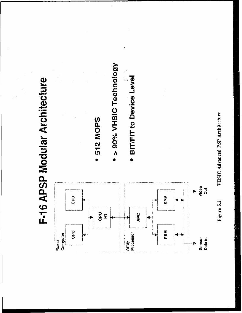
"0 "
0
U) A
0 > -
__u 04
ItO A
0•,
CLt O) ............. ............. ..... .....
....... .: .. .. . . . . . . ... .. ..
- V I iI.
LII. ......... F
I-.. I
n nI II II II
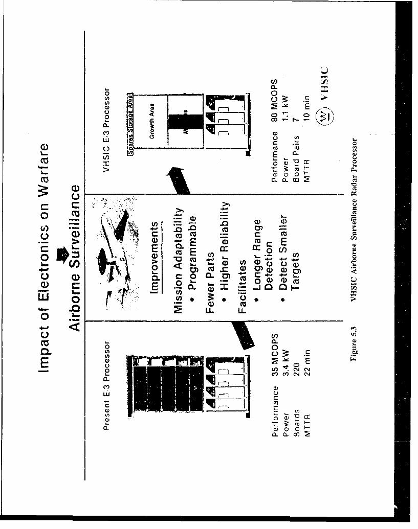
0 0CD~ -x.
C) 0
W co
oo
0 -
CP
0.) cu
EE00
LCL
0)
CHAPTER 5 - TECHNOLOGY INSERTION
Westinghouse is also using the same VHSIC technology on classifiedprograms. One, in particular, has a requirement for hundreds of array processorsperforming over a hundred billion operations per second and requiring more thantwo hundred million bytes of memory.
In summary, the application of VHSIC technology has provided important
benefits to DoD systems. Specific benefits for specific systems such as (1) lowweight in AH-4 helicopter applications, (2) fault tolerance for ARSR-4
remote/unattended operation, and (3) improved performance within the samevolume and power constraints for the AWACS, have all been attained. In theF-16, software compatibility with existing operational flight programs was anabsolute requirement. In other crnvironments, the ability to do multi-sensor
processing with the same signal processing module significantly eases logisticsupport. Lower cost and higher reliability have been achieved in all cases.
182

CHAPTER 6 - TECHNOLOGY TRANSFER
6.1 Training . ................................................... 184
6.2 Conferences and W orkshops .................................... 1866.2.1 VHSIC Annual Conferences ................................. 1866.2.2 Topical Conferences and Workshops .......................... 186
6.3 Technology Transfer of Design Tools . ............................. 190
6.4 Testability and Built-In-Self-Test ................................. 191
6.5 Com mercial Applications . ....................................... 1926.5.1 Desktop Supercomputers Using VHSIC ....................... .192
183

CHAPTER 6
TECHNOLOGY TRANSFER
The VHSIC Program Office recognized, from the outset, that the transfer of VHSICtechnology and products to both the DOD contractor community and DOD acquisitionmanagers was essential for program success. It also recognized that historically this had beena difficult task to achieve. Novel approaches were needed to ensure that system designerswould not only have access to VHSIC technology but also to VHSIC software and devices asquickly as they became available.
Technology transfer has been effected through information disscmination, militaryweapon system technology insertion projects, VHSIC program sponsored training courses,conferences and workshops, and transfer of some VtSIC developed state-of-the-art designtools, testability concepts, and other critical technologies to industry, universities, and non-military Government agencies. Some commercialization of VHSIC technology has alsooccurred.
A major source of information for the defense community is and will continue to bethe Defense Technical Information Center (DTIC). DTIC has on file well over 1000documents relative to VHSIC end VHSIC related technology. DTIC is accessible to qualifiedusers, including U.S. Government agencies, their contractors, subcontractors, and potentialcontractors who have established a "need to know" at DTIC.
A special issue ot the "APL Technical Review", published by the Johns HopkinsUniversity Applied Physics Laboratory, is devoted to V\HSIC. It provides a series of invitedarticles covering the areas of VHSIC technology and chip sets, design methodology, technologyinsertion, system considerations, VHSIC tools, and system life-cycle suppoitability. SeeReference 6.1.
The various aspects of VHlSIC technology transfer are discussed in the followingsections of this chapter.
6.! Tra-i.ngS
The VIISIC training program began in January 1984 in order to provide:
o system managers and senior engineers with an awareness of the VHSICproducts and design technologies being developed, and
o working level engineers with instruction in the design of systems usingVIISIC products through hands..on design workshops.
The primary techniques for accomplishing these objectives have been regional work-shops, conferences, presentations. and brochures. For the hands-on workshops, specialsoftware has been developed for using VItSI(" design tools, and detailed technical reference
184
CHAPTER 6 / TECHNOLOGY TRANSFER
material has been prepared in the form of application notes, performance data sheets, and textbooks.
VHSIC Application Workshops were organized and held throughout the country on aregion,.! basis. The workshops provided comprehensive training and education in VHSICtechnology for defense contractor personnel for the purpose of accelerating the application ofVHSIC technology in military electronics. More than 3000 engineers and technical managershave attended them. Over thirty such workshops were held from 1984 through 1986.
The scope and depth of coverage of VHSIC technology at these workshops haveenabled each attendee to evaluate the feasibility of using VHSIC technology in specificmilitary system applications. Attendees were given the opportunity to present bothapplication and work-related problems which were discussed by the group in terms of howVHSIC can be applied. The attendees were provided with approximately three days ofinstruction using text material which they took with them for future use in electronic designand for interface with the VHSIC community.
The instructional material (available from DTIC) included:
o Student Guide - a compilation of VIISIC design data and chiparchitectures. DTIC No. AD-B088-098
o VHSIC Specification Guide - an abbreviated version of all of the VHSICchip specifications. DTIC No. AD-B088-097
* Interface Reference Guide - a collection of technical and managementinformation about ICs, Computer Aided Design (CAD) availability, docu-ments available, as well as key Government and industry personnel.DTIC No. AD-B088-099
A number of similar workshops have been held for DOD and other Governmentpersonnel at such in-house facilities as the Naval Ocean Systems Center (San Diego), theNaval Weapons Center (China Lake), Eglin Air Force Base (Florida), and the NASA JohnsonSpaceflight Center (I louston).
A major follow-on effort to the Applications Workshops was developed by the !ohnsI1opkins University Applied Physics Laboratory and was initiated in June 1985. Called "Appli-cations !I", it was intended for those system designers who had attended the regionalworkshops. It built on their knowledge from earlier workshops and concentrated exclusivelyon how to design electronic suhsystenis using VI ISIC products. This two day training programallowed hands-on use of some of the CAI) tools developed for the VIISIC Program. FourApplications II workshops were held during the summer of 1985. Further extensions of theseworkshops were Applications III held by JlItJ/APL in October 1986, The Advanced Hands-0)n Applications Woikshop IV (or VIHSIC Tech-Fair) held in July 1987, and VHSIC Tech-Fair II. co-sponsored by the Dol) VIISIC Program Office, the Defense Systems ManagementCollege, and JIIU/APL in June 1988.
185
CHAPTER 6 / TECHNOLOGY TRANSFER
Other training workshops, seminars, and courses held have included the following:
"o IDAS Workshop, sponsored by the DoD VHSIC Program Office, held at Universityof Cincinnati, Cincinnati, O11, August 19-21, 1987
"o VHDL Users Group Workshop, sponsored by the DoD VHSIC Program Office,held at Virginia Polytechnic University, Blacksburg, VA, October 20-22, 1987
"o Seminar on VHSIC Technology and Applications Design, sponsored by PalisadesInstitute for Research Services, November 3-5, 1987
"o VHDL Tutorial, sponsored by the IEEE, ICCAD, Santa Clara, CA, November 9,1987
The following training courses and materials were available as of September 1990:
o VHDL training courses, offered by CAD Language Systems, Inc. Call (301) 963-5200.
o VHDL training courses, offered by Intermetrics. Call (617) 661-1840.
o ADAS Training Course, offered approximately six times a year by CadreTechnologies. Call (401) 351-5950
6.2 Conferences and Workshops
6.2.1 VHSIC Annual Conferences
From 1982-1987, the VIISIC Program Office spo-nsored annual three-day conferencescovering all major aspects of the VI ISIC program. A final one-day VHSIC Conference washeld in November 1989. Proceedings of these corfcrences (with identifying DTIC numbers)are listed as References 6.2 through 6.8.
6.2.2 Topical Conferences and Workshops
In addition to the comprehensive VIISIC Annual Conferences, topical meetings andworkshops were held covering the following specific VIISIC areas.
(0) P;•,,ckq i o1V
(b) Qualification, Reliability, and Logistics,
186
CHAPTER 6 / TECHNOLOGY TRANSFER
(c) VHSIC Hardware Description Language (VHDL)(d) Tester Independent Support Software Systems (TISSS)(e) Engineering Information System (EIS)(f) VHSIC Applications
(a) Packaging
o 1985 VHSIC Packaging Workshop, Naval Surface Weapons Center, Silver Spring,Maryland, June 5-6, 1985. Proceedings available from Palisades Institute forResearch Services.
o 1986 VHSIC Packaging Workshop, Plymouth, Minnesota, September 15-17, 1986.Information available from Owen Layden, Army LABCOM, 201-544-2378.
o 1987 VItSIC Packaging Conference, April 21-22, 1987
o 1988 VHSIC Packaging Conference
o Tri Service Packaging/Interconnections Conference, Ft. Monmouth, NJ, May 1989
(b) Qualification. Reliability, and Logistics
o 1985 VIISIC/VLSI Qualifications Workshop, Vail, Colorado, September 18-20,1985. Proceedings available fiom Palisades Institute for Research Services.
o 1986 VIISIC/VLS1 Qualifications Workshop, Vail, Colorado, September 9-12, 1986.Proceedings available from DTIC: Nos. AD-13110-746,-747, -748, and -749.
o 1987 VHSIC Qualification, Reliability, and Logistics Workshop, sponsored by theDoD VIISIC Qualification Committee, Colorado Springs. August 25-27, 1987 _
* 1988 VIlSlC/VLSI Qualification, Reliability, and Logistics Workshop, sponsoredby the DoD VIISIC Qualification Committee, Scottsdale, Arizona, September 27-29, 1988. Proceedings available from Analytics, Inc.
o Advanced Microclcctronics Technology, Qualification, Reliability and LogisticsWorkshop, Alberquerque, NM, August 29-31, 1989.
187
CHAPTER 6 / TECHNOLOGY TRANSFER
(c) VHSIC Hardware description Language (VHDL)
The following meetings were sponsored by the VHDL Users' Group. This group,established in April 1988, organizes and sponsors meetings on VHDL, publishes a regularnewsletter, and maintains an electronic bulletin board system for information exchange.
"o VHDL Users' Group Meeting, at the Design Automation Conference, Anaheim,CA, June 26, 1988
"o VHDL Users' Group Meeting, Redondo Beach, CA, October 23-26, 1988
"o VHDL and Modeling in the DoD Procurement Process, Washington, D.C., June21-23, 1989
"o VHDL and the Design Environment, Redondo Beach, CA, October 22-25, 1989
"o VHDL: The Emerging D,£Xign Standard, Boston, MA, April 4-6, 1990
"o VHDL Users' Group Third Annual Fall Meeting, San Jose, CA, October 1990
The following meetings on VHDL were sponsored or co-sponsored by the IEEE andother organizations.
"o VHDL Users' Workshop, Charlottesville, VA, IEEE sponsored, April 18-20, 1988
"o VHDL Developers Forum, Charlottesville, VA, September 14-16, 1989
"o VHDL Forum for CAD, Munich, West Germany, IFIP sponsored --- kickoff ofEuropean VHDL Users' Group, November 23-24, 1989
"o VHDL: The Standard Language in the CAE Environment, Jerusalem and RamatGan, Israel, Israel Society for CAD/CAM and Israel Ministry of Defense sponsored,December 14, 17, 1989
"o First European Working Conference on VHDL Methods, Marseilles, France, IMT,IEEE and AFCET sponsored, Sep 4-7, 1990
In addition, every major IC design conference in the industry has had one or morespecial sessions on VHDL over the past few years. Of note are tile sessions in manufacturingand other technology conferences where VHDL's impact on the engineering design process isbeing reported.
188
CHAPTER 6 1 TECHNOLOGY TRANSFER
(d) Tester Independent Support Software System (TISSS)
"o Industry Review, Melbourne, FL, September 1987"o Industry Review, Phoenix, AZ, January 1988"o Industry Review, Orlando, FL, May 24-25, 1988"o Hands-on-Training, RADC, Rome, NY, June 1988
(e) Engineering Information System (EIS)
"o IEEE Design Automation Conference, Apache Junction, AZ, January 1, 1988"o COMPCON, San Francisco, CA, February, 29, 1988"o CAD Frameworkshop Standards Workshop, May 26, i988"o EIS Workshop, Baltimore, MD, November 14-18, 1988"o COMPCON, March 1, 1989
(f) VHSIC Applications
"o Navy VHSIC Users Symposium, Johns Hopkins University Applied PhysicsLaboratory, Laurel, Maryland, April 26-27, 1983. Report JHU/APL/SR-83-2,Contract N00024-83-C-5301. Proceedings available from DTIC: No. AD-C032-934.
"o VHSIC Signal Processing Seminar, Naval Postgraduate School, Monterey, CA,June 17-18, 1986
"o Proceedings of the VIISIC Advanced Applications Workshop III, Johns HopkinsUniversity Applied Physics Laboratory, Laurel, Maryland, October 29-30, 1986
"o VHSIC TECH-FAIR (Advanced Hands-On Applications Workshop IV),cosponsored by the DoD VHSIC Program Office and the Johns Hopkins UniversityApplied Physics Laboratory, Laurel, Maryland, June 30-July 2, 1987. Informationavailable from JHU/APL
"o VHSIC TECH-FAIR II, cosponsored by the DoD VHSIC Program Office, theDefense Systems Management College, and the Johns Hopkins Applied PhysicsLaboratory, Laurel, Maryland, June 28-30, 1988. Information available fromJHU/APL.
"o Government Microcircuit Applications Conferences (GOMAC) 1978-1989. Includespapers on VHSIC applications in general sessions, topical sessions, and specialsessions for VHSIC applications. Digests of Papers are available from DTIC asfollows:
189
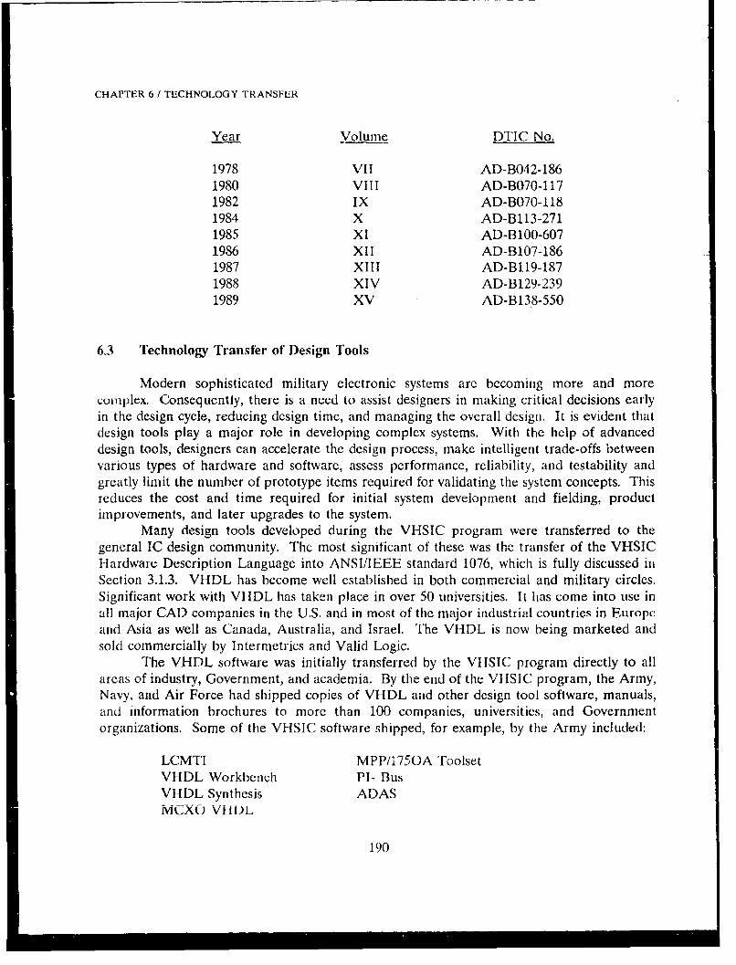
CHAPTER 6 / TECHNOLOGY TRANSFER
Year Volume DTIC No.
1978 VII AD-B042-1861980 VIII AD-B070-1171982 IX AD-B070-1181984 X AD-B113-2711985 XI AD-B100-6071986 XII AD-B107-1861987 XIII AD-B119-1871988 XIV AD-B129-2391989 XV AD-B138-550
6.3 Technology Transfer of Design Tools
Modern sophisticated military electronic systems are becoming more and morecomplex. Consequently, there is a need to assist designers in making critical decisions earlyin the design cycle, reducing design time, and managing the overall design. It is evident thatdesign tools play a major role in developing complex systems. With the help of advanceddesign tools, designers can accelerate the design process, make intelligent trade-offs betweenvarious types of hardware and software, assess performance, reliability, and testability andgreatly limit the number of prototype items required for validating the system concepts. Thisreduces the cost and time required for initial system development and fielding, productimprovements, and later upgrades to the system.
Many design tools developed during the VHSIC program were transferred to thegeneral IC design community. The most significant of these was the transfer of the VHSICHardware Description Language into ANSI/IEEE standard 1076, which is fully discussed inSection 3.1.3. VItDL has become well established in both commercial and military circles.Significant work with VHDL has taken place in over 50 universities, It has come into use inall major CAD companies in the U.S. and in most of the major industrial countries in Europeand Asia as well as Canada, Australia, and Israel. The VHDL is now being marketed andsold commercially by Intermetrics and Valid Logic.
The VHDL software was initially transferred by the VIISIC program directly to allareas of industry, Government, and academia. By the end of the VHSIC program, the Army,Navy, and Air Force had shipped copies of VHDL and other design tool software, manuals,and information brochures to more than 100 companies, universities, and Governmentorganizations. Some of the VHSIC software shipped, for example, by the Army included:
LCMTI MPP/175OA ToolsetVHDL Workbench PI- BusVHDL Synthesis ADASMCXO VH-iDL
190
CHAPTER 6 / TECHNOLOGY TRANSFER
In addition to the direct insertion of the VHDL software, the joint program with theCanadian Government, described in Section 3.1.3, aided the technology transfer process bydeveloping industrial design practices around VHDL. It also developed additional desigi- toolsand adapted the software for operation on additional high performance workstations.
Another design technology transfer has been the Tester Independent Support SoftwareSystem (TISSS) described in Section 3.2.2. TISSS began as a VHSIC program with continuedfunding by the Advanced Tactical Fighter Program in the Air Force. During the developmentof TISSS, a procedure was evolved for describing test vectors and test waveforms. Thespecification for this procedure is being considered as IEEE Standard 1029.1 - Waveform andVector Exchange Specification. Several DoD programs are already using preliminary versionsof this specification. The TISSS software itself is being transitioned by the Air Force directlyto Air Force Logistics Centers as well as the Defense Electronic Supply Center.
Other VHSIC developed tools that have been transitioned as commercial products arethe Architecture Design and Assessment System now marketed by CADRE, and the JRSResearch Integrated Design Automation System.
The JRS Research tool set which synthesizes a processor architecture from the Ada or"C" application program, generates the VHDL model of the processor, and uses the model toautomatically generate the compiler for the architecture is a unique capability not availablefrom other sourcc., and funded almost completely by the VHSIC program. This tool is nowin use on several DoD programs and one commercial company.
The Engineering Information System funded by the VHSIC program has transitionedmany concepts to industry through close association with the CAD Framework Initiative. TheEIS prototype is being transitioned directly to the Sacramento Air Logistics Center as anEngineering Data Management System for the Air Force Advanced Tactical Fighter program.
6.4 Testability and Built-In-Self-Test
The increasing emphasis on built-in-test and built-in-self-test in the IC designcommunity stemmed from the early VHSIC efforts with industrial and university contractorsto develop efficient and economical methods of testing very complex ICs after they weremanufactured and after they were installed in systems.
The testability concepts implemented by the VHSIC contractors in the area of testablecircuit design are presently being used in many commercially available ICs. Several ASICvendors presently include Scannable Sequential Elements in their design libraries.
Part of the effort on BIT and BIST led naturally to the development of the VHSIC testbus interoperability standards - the TM-Bus and the ETM-Bus which are discussed fully inSection 3.1.2. These standards have become the focus of steps toward establishing an industry-wide, IEEE set of standard test busses.
191
CHAPTER 6 / TECHNOLOGY TRANSFER
6.5 Commercial Applications
6.5.1 Desktop Supercomputers Using VHSIC
Commercial versions of VHS1C technology have been used to develop a series of low-cost, desktop supercomputers. The QUEN family of array processors was inaugurated at theIEEE Workstations Symposium held at the Johns Hopkins Applied Physics Laboratory(.IHU/APL) in October 1989. Both the 1.25 micron, 25 megahertz technology and the efficientmassively paraIJel array architecture are products of the VHSIC Program.
The QUEN processor, developed at JIIU/APL, under Independent Research andDevelopment funding, in conjunction with the VHSIC Program, brings low costsupercomputing to the desk top. It is the first available, commercial, parallel processor tobring CRAY 1 computation speeds into the minicomputer price range.
The QUEN approach to high speed computation uses the Memory-linked WavefrontArray Processor technology. Based on the concept of waves of computation traveling throughan array of processors, it was created to provide high speed solutions of numerically intensivecomputational algorithms. In its most general form, the array is configured as an n-dimensional mesh of processors, each onerating as an independent unit executing instructionsstored in its private, local program memory. Data for each processor is contained inmultiport memories connected to the adjacent processor on its boundaries. Computation anddata flow in the mesh are controlled with haidware synchronization structures in eachmultiport memory.
The first processing implementation used all commercial logic chips and required 3circuit boards. Each multiport memory required an additional circuit board. Once feasibilityhad been established, the first prototype memory/processing element module was developedusing the VHSIC multiport memories from TRW and FPMAK qrithmetic elements developedwith VHSIC features by Raytheon. This unit operated at 10 Mllz and required 2 circuitboards per memory/processing element. The technology was then transferred to InterstateElectronics Corporation for insertion into the commercial market. I tere, a different approachwas used for implementing the processor. Instead of using VHSIC components for thearithmetic elements, commercial VLSI chips were used with the interconnection logic done inV1HSIC technology gate arrays. The large pin counts and density of VHSIC gate arrayspermitted a single gate array chip to implement interconnection logic for both the memoryand processing elements. The result was a single board module containing up to 128k wordsof 32-bit memory and 16k words of program memory, operating at 20 million floating pointoperations per second. In addition the cost of the unit was reduced by a factor of 2.
Today a family of QUEN Array Processors based on commercial spin offs of VHSICtechnology is being marketed for commercial and military applications by InterstateElectronics Corporation. The processors are available embedded in an Intelligent Imagingsystem, and as attachments to VAX/VMS host computers or Suit workstations. The membersof this family of processors are differentiated by the number of processing elements in asystem. The largest unit provides 1.28 billion floating-point opcrations per second and thesmallest 80 million. Two units, each capable of 128 million floating-point operations per
192
CHAPTER 6 / TECHNOLOGY TRANSFER
second, are installed at The Applied Physics Laboratory. One unit is installed on theJHU/APL computer network for general use while the other is used for sonar signal andimage processing.
The use of VHSIC technology in this application reduced the size and cost of the unitand increased its processing speed, both by a factor of two. In addition, it increased systemreliability and made comprehensive system testing possible. The QUEN supercomputer is asuccessful example of "dual use" technology. DoD developments are being used to meetDefense systems needs as well as to enhance the capabilities and competitiveness of U.S.commercial technology.
193
CHAPTER 7 - VHSIC INDUSTRIAL BASE
The Impact of VHSIC at IBM: A Case Study- Robert H. Estrada and Harley A. Cloud ............. ....... 197
7.1 Design and Manufacturing Capabilities ............................ 2007.1.1 AT&T M icroelectronics ................................... 2007.1.2 H oneywell ............................ ................. 2017.1.3 Hughes Microelectronics Centers - Carlsbad and Newport Beach ..... 2017.1.4 IB M . . .. . .. . . . . . . . . . . . . . . . . . .. . . .. . . . . . . . . . .. . . . . . . . . 2027.1.5 LSI Logic uorpolation .................................... 2037.1.6 M otorola .............................................. .2047.1.7 National Semiconductor Corporation ......................... 2057.1.8 Performance Semiconductor Corporation ....................... 2067.1.9 Raytheon Com pany ...................................... 2067.1.10 Silicon Compiler Systems .................................. 2077.1.11 Texas Instrum ents ....................................... 2087.1.12 TRW .................................................. 2097.1.13 United Technologies Microelectronics Center .................... 2117.1.14 VTC Incorporated ....................................... 2117.1.15 Westinghouse - Advanced Technology Division .................. 212
7.2 Commercially Available VHSIC Design Tools ........................ 213
The Impact of VHDL on Design Automation Tool D)evelopment, Acquisition,
and Use - Randolph E. Harr ................................ 213
Sim ulators/Analyzers .......................................... 2207.2.1 D azix ... ... . ... ..... .. . ... ... .. . ... .. . .... . ... ... . ... 2207.2.2 E xpertest . ... ....................... ............... .... 2217.2.3 Interm etrics . ............................................ 2217.2.4 M entor G raphics ........................................ 2217.2.5 Microelectronics and Computer Technology Corp .................. 2217.2.6 T eradyne .............................................. 2227.2.7 V alid Logic Systems, Inc .................................. 2227.2.8 V antage A nalysis ........................................ 2227.2.9 V iew Logic System s ...................................... 2227.2.10 Z ycad ... .. . . .. . .. .. ... ... ... ... .. . ... .. . ..... . ... . ... 223
H ardware Accelerators ......................................... 2237.2.11 Ikos System s .......................................... 2237.2.12 Z ycad . . . . . . . . . . . . .. . . . . .. . . . . . . . . . . . . . . . . . . . . . . .. . . . . 223
195
Synthesis .. . .. . ... . ... ... ... ... . ... . ... ... . .. . .... ... . ... ... 2237.2.13 JRS Research Laboratories ................................. 2237.2.14 Silc Technologies, Inc .. .................................... 2247.2.15 Silicon Compiler Systems . .................................. 2247.2.16 Synopsys, Inc .. .......................................... 2247.2.17 Trimeter, Inc .. .......................................... 224
M odeling . ................................................... 2257.2.18 EIS M odeling, Inc ....................................... 2257.2.19 Logic Autom ation ....................................... 2257.2.20 LSI Logic Corp ......................................... 2257.2.21 Quadtree Software Corporation .... .......................... 2257.2.22 VLSI Technology, Inc ...................................... 226
Integration and Adaptation ..................................... 2267.2.23 Cadence . .............................................. 2267.2.24 CAD Language Systems .................................... 2267.2.25 Cadre Technology ....................................... 2277.2.26 Fintronic, USA ........................................... 2277.2.27 Gateway Design Automation ............................... 2277.2.28 GenRad Incorporated ...................................... 2277.2.29 Ilogix, Inc ............................................... 2287.2.30 Research Triangle Institute . ................................. 2287.2.31 Silvar-Lisco ............................................ 2287.2.32 Vista Technologies . ....................................... 228
196
i I I I I=Now
CHAPTER 7
VHSIC INDUSTRIAL BASE
It is evident that the system insertions and technology demonstrations of the VIHSICProgram described in Chapters 4 and 5 have had a major imnoact on DoD systemdevelopments. Not only have the new hardware components gone into new systems but thetechniques for designing complex chips and subsystems are being increasingly automated.Design automation is necessary in order to be able to handle the enormous amount of datarequired to design them accurately within reasonable time and cost limits. To support boththe fabrication and design activities, an increasing number of companies are providingproducts and services which meet VHSIC requirements and which have become generallyavailable to the defense community.
The impact of the VHSIC program on the industrial base is illustrated by the papercontributed by two VHSIC program managers from one of the largest members of the U.S.semiconductor industry. The sections following the paper describe the VHSIC manufacturingand design capabilities of a number of companies that responded, as of March 1990, to arequest for such information. The descriptions are brief and are intended only to illustrate thegeneral capabilities available at the time this report was written. For more detailed, specific,up-to-date information, direct contact with the companies is necessary.
The Impact of VHSIC at IBM: A Case Study
Robert H. Estrada, IBM VHSIC Program Managerand
Harley A. Cloud, University of Maryland(Former IBM VHSIC Program Manager)
IBM has been a participant in both Phase 1 and Phase 2 of the DoD VHSICprogram. Over the ten year period of the VHSIC program it has provided IBMwith the motivation and focus for establishing a semiconductor design andfabrication facility which meets the electronic technology needs of DoD systemsand, which, at the same time, has interacted positively with its commercialsemiconductor activities. Under this impetus, IBM enhanced its ability to designstrategic and tactical systems, made the corporate commitment to establish amilitary IC pilot line that would be accessible to the military contractor community,and has incorporated many of the VHSIC technology advancements into ICproducts for space and tactical applications. The development of the VHSICtechnology under the management of the DoD program offices has proven to be thecritical integrating element for establishing these capabilities.
197
CHAPTER 7 / VHSIC INDUSTRIAL BASE
Under the VHSIC program, the major objectives and associated results atIBM can be summarized as F61 ows:
o Established a 1.25 micron NMOS technology - 1982
o Established a 1.0 micron CMOS technology - 1985
o Established a 0.5 micron CMOS technology by scaling 1.0 micron CMOSto 0.5 micron CMOS - 1987
o Established an operational pilot line capable of producing VHSIC chipsat 1.25, 1.0, and 0.5 micron levels meeting all DoD technicalrequirements, i.e. FTR, density, performance, etc.
o Established an automated design capability and operational pilot/foundryline at both 1.0 micron and 0.5 micron which meet VHSIC technicalrequirements. These facilities were made available for users within IBMand the DoD contractor community in 1988.
o Provided for the use of VHDL in both military and commercial designprocedures in 1987 with full validation projected to be completed in 1990.
In undertaking the VHSIC program, IBM adopted a conservativedevelopment plan for Phase 1 by first establishing the design and fabricationcapabilities needed to provide VHSIC products and support and then demonstratingthese successfully in 1984 with a single, very advanced chip design using NMOStechnology. This chip, identified as the Complex Multiply and Accumulate(CMAC), had 37,000 gates and 101,000 transistors, was 8 millimeters square, andperformed very complex digital signal processing. VHSIC Phase 1 proved to beextremely valuable to IBM in learning how to produce such an advanced level ofmilitary IC technology reliably and efficiently.
As a result of the Phase 1 effort, IBM realized that the NMOS technology,though adequate for Phase 1, would not be able to meet the performancerequirements anticipated for VHSIC Phase 2 or, more importantly, for futuresystems in general. IBM therefor made an internal transition from the 1.25 micronNMOS process to a 1.0 micron CMOS process which had been under developmentfor commercial use. The 1.0 micron CMOS technology is now used in all of ourproducts for DoD systems. The 1.0 micron CMOS process also served as 2 basisfor the VHSIC Phase 2 program along with the Phase 1 design libraries and designtool methodology. The migration from NMOS to CMOS at IBM was acceleratedby at least a year as a result of the VHSIC experience and was one of the mostnotable impacts of the VHSIC program.
A conservative fabrication approach was again chosen for Phase 2. The 1.0micron CMOS technology was used with the MOS transistor gates scaled down to0.5 micron in order to meet the VHSIC requirements for density, performance, andi-1K. I he design program, however, was a more ambitious effort than Phase 1.
198
ClAPTER 7 1 VHSIC INI)USTRIAL BASE
Several chip types of different size, function, and performance were developed.'These chip capabilities and associated brassboards were successfully demonstratedin December 1988.
In addition to the overall focus on the design and production of military ICswhich VHSIC has provided, the program has also given much needed direction tothe industrial community on the solution to many specific technical IC design andfabrication problems which are important for military systems. One of the mostcrucial of these problems is that of achieving the radiation hardness that is requiredfor military equipments in tactical and strategic warfare conditions. Results in thisarea have been excellent. The radiation hard processing technology developed atIBM under VHSIC has been incorporated into the standard fabrication schedule forall military ICs with no appreciable increase in processing cost. The same processcan also be used effectively in selected commercial applications such as space.
VHSIC has emphasized the use of test chips having structures on themcarefully designed to provide data that predicts the performance, reliability,radiation effects, and yield of subsequent product chips. These test chips haveprovided excellent projections on how producible the tested technology will be.The VHSIC test chips and the data they provide has enabled IBM to constructmore accurate yield and reliability models than heretofore. This concept is beingfurther developed as the approach to the "generic" qualification of IC productionlines an effort which IBM strong.y supports and is introducing into itsproduction lines.
Packaging has been another key element of VHSIC emphasis. In order tomeet the stringent VHSIC requirements, both single chip and multi-chip packageswith very high I/O counts had to be developed. These packages have evolved intomany products that IBM is producing for use in weapon systems as well as futurecommercial products.
VHSIC technology has made it possible for many advanced, multipurposeprocessing architectures to be realized for space, avionic, tactical, and strategicapplications. The architectures emphasize real time processing, very highthroughput, extensive instruction sets in a variety of environments from benign toextreme such as that needed in certain space applications. A key factor in thisdevelopment has been the design and fabrication of a large family of genericmultifunction chips in 1.0 micron CIMOS technology. Over 40 product chips havebeen produced, many of which serve as the bases for subsystem level hardwaremodules that can be configured into systems using an Ada based supportenvironment. In addition, dutomatic scaling of the 1.0 micron designs to 0.5micron (FET gate length) has been demonstrated. This allows the production ofhigher speed ci .: 'or use in system upgrades and future applications.
The desig-. and optimization of such architectures required the developmentof design and analysis tools such as the VHDL and built-in-test circuitry bothof which have received high priority under VHSIC. IBM has been using andinserting these VI-ISIC technologies into a variety of military and commercialprograms.
VIISIC has been an outstanding and productive program with many positiveaccomplishments achieved directly under the poogram sponsorship but also withmany side benefits for corporate itMVi. The V-HSiC program cdme ionrig .L jubL Lim:
19C)
CHAPTER 7 / VHSIC INDUSTRIAL BASE
right time. The objectives established by DoD strongly influenced our decision toP tablish e semi -conductor capabili for providi, - the advanced technologyneeded in future DoD systems. The objectiwes were a.so consistent with our longterm crrrocictal activities. The VHSIC activities within IBM could therefore besmoothly coordinated among four IBM corporate facilities. The program wasmanaged and carried out primarily by the Federal Sector Division at Manassas,Virginia. Major contributions to the technology development were funded by IBMat the General Technology Divisions in Burlington, Vermont, and E. Fishkill, NewYork. The Thomas J. Watson Research Laboratory at Yorktown Heights, NewYork, also provided basic research and development support.
These coordinated activities were strongly focused and directed by the goalsand schedule of the VHSIC program. The character and course of IBM's corporatepolicies and plans for advanced ICs for military use have been substantiallymodified and accelerated as a result of its participation in the VHSIC program.
7.1 Design and Manufacturing Capabilities
7.1.1 AT&T Microelectronics
o Fabrication process- 1.25 micron bulk CMOS, 5 V, radiation hard; QML certified; single and double
level metal interconnect
o Devices for sale- Bulk CMOS, radiation hard, 256k and 64k SRAMs
o Form- DIP, 24-pin, 600-mil ceramic package
o Services available- Foundry
o Point of contactEdward J. Schmitt 201-771-4300Manager, Military/AerospaceMarket DevelopmentAT&T Microelectronics2 Oak WayP.O. Boy 610Berkeley Heights, NJ 07922
200

CHA"TER 7 / VtiSC INDUSTRIAL BASE
7.1.2 Honeywell
o Fabrication processes1.25 micron bulk CMOS, radiation hard; QML certification in 1990
- 0.8 micron silicon-on-insulator CMOS, radiation hard; in development
o Devices for sale- Static RAMs, 16 to 64k- Digital gate arrays, 15k gates, radiation hard; VIIDL model available- Standard cells, radiation hard; VltDL model available- Test bus interface unit, compatible with TM Bus Interface Specification,
Version 3.0; VIIDL model available
o Form- 'GA, LLCC, LCC, and hybrid packages available; pin counts 14 to 284 pins- Customn packaging
o Design capability- Range from gate to mask level designs
o Other servicesEntry points range from net list to foundry-VHDL. capabilityApplications engineeringDesign training seminars and workshops
* Points of contact- George Anderson (Radiation H lard Devices) 612-541-2045- Charles Hudson (Test Flus Interface) 612-541-2185- David Wick (Silicon Compiling) 612-541-2801- Michael Caruso (Applications[Training) 612-541-2198
ltoneywcll Solid Statz Electronics (Center12001 itighway 55Plymouth, MN 55441
7.1.3 Hughes Microeledronics Centers - Carlshad and Newport Beach
o Fabrication processes- 1.25 micron CMOS/SOS. 3.3 to 5 V, radiation hard- 1.1 micron CMOS, radiation hard
0.9 micron CMOS, radiation hardening in development
201
CHAPTER 7 / VFISIC INDUSTRIAL BASE
" Devices for sale- Multi-channel correlator- Single channel correlator- Signal tracking subsystem- Static shift register- Standard cell semi-custom devices- Configurable gate arrays
"o Forms- Chip- Single chip packages including PGA, LCC, LLCC, and quad flatpacks- Multichip packages
"o Design capabilities- Standard cell, full custom, structured-custom cell, and gate array- RAM, ROM, and PLA generators- Mentor Graphics and CALMA workstations- Design entry from behavioral, RTL, or logic description- VHDL capability expected in 1990
"o Other Services- Foundry service from CALMA tapes
"o Point of contact- R.W. Dodge 619-931-3196
Hughes Microelectronics Center6155 El Camino RealCarlsbad, CA 92009
7.1.4 IBM
o Fabrication processes- 1.0 micron CMOS, 5 V, DESC certified 12/11/87- 1.0 micron CMOS, 5 V, radiation hard
- 0.5 micron CMOS baseline, 3.3 V- 0.5 micron CMOS, 3.3 V, radiation hard
* Devices for sale- Configurable SRAM- Bus Interface Unit- Systolic Processor
202
CHAPTER 7 / VHSIC INDUSTRIAL BASE
- Address Generator- Signal Processing Element- 64k radiation hard SRAM- 256k radiation hard SRAM (engineering samples)- Fourier transform module boards- Generic VHSIC Spaceborne Computer chip set- Common Signal Processor chip set
Radiation hard Vector Processor brassboards- Radiation hard 32-bit Processor (in development)
"o Form- VHSIC chip on silicon- Single chip package- Multi chip package- C4 flip chip- Wirebond
"o Design capabilities- VHDL design capability 4Q90- Custom, master image, gate array to 70k gates- Subsystem and system level entry points- Chip/system simulation (Hardware Accelerator)
" Other services- Foundry: chip design, simulation, mask procurement, chip fabrication, and
LSSD test methodology
"o Points of contact- Philip B. Johnson (Program Manager) 703-367-5547- Jay Harford (VHSIC Marketing) 703-367-1041
IBM Federal Systems9500 Godwin DriveManassas, VA 22110
7.1.5 LSI Logic Corporation
"o Fabricati(,n Process1.0 micron CMOS, 5 V
"o Devices for saleGate arrays to 100k
203
CHAPTUh 7/ VHSIC INDUSTRIAL BASE
Standard cell based ASICsSPARC (scalable processor architecture) 32-bit RISC CPUSingle chip floating point unit for SPARC-Combined MMU, cache controller, cache tags for SPARC
- MIPS architecture 32-hit RISC processor with memory management- MIPS architecture 32-bit floating-point processor- MIPS architecture read-write buffer- 32-bit IEEE floating point processor- 8-bit error correcting Reed-Solomon Codec
o Form- Chip and single-chip package
o Other services- Design development tools with associated training courses- VHDL models (under development)
o Point of contact- Joe Ferro 408-434-6422
Manager, Strategic Military ProgramsLSI Logic Corporation48660 Kato RoadFremont, CA 95438
7.1.6 Motorola
"o Fabrication processes- 1.2 micron CMOS, 5 V, 3-level metal, single layer poly- 0.8 micron CMOS available late 1990- Certification for wafer fabrication facility scheduled for 1990; back-end facilities
(package and test) are currently certified.
"o Devices for sale- High density gate array family, 3k to 105k gates; RAM/ROM capability- Custom bipolar and CMOS
o Form- Single chip packages: chip carriers, quad fiat pack, and pin grid arrays
o Design capabilitiesDesigns accessible through Mentor/Sun workstations at the schematic entrylevel
204
CHAPTER 7 / VltSIC LNDUSTRIAL BASE
o Other services- VHDL models for gate arrays (under consideration)- Foundry (CALMA database supplied by customer)
o Point of contact- Dick Hurley 602-897-3782
MS EL-376Motorola, Inc.Military Products Operation2100 E. Elliott RoadTempe, AZ 85284
7.1.7 National Semiconductor Corporation
"o Fabrication processes- 0.8 micron CMOS, 5 V; in process of certification as beta site, within QML
program- 0.8 micron BiCMOS, 5 V- 0.8 micron ECL, 5 V
"o Devices for sale- CMOS standard cells up to 80k gates- ECL and CMOS gate arrays from 7.5k to 250k
"o Form- Chips and single packages: PGA, DIP, leadless and leaded chip carriers
"o Design capabilities- National DA4 design automation software- VHDL simulation capability available through Vantage Analysis- Additional VHIDL simulation under development in conjunction with Silicon
Compiler Systems and Verilog- GENESIL compiler supports CMOS processes- Design entry through National DA4, customer's workstation, or GENESIL
compiler
"o Other Services- Design tool training
"o Point of contact- Kirk Lemon 4,08-721-4172
Military/Acrospace ASIC Marketing Manager
205

CHAPTER 7 / VHSIC INDUSTRIAL BASE
National Semiconductor CorporationMS 10-1052900 Semiconductor DriveSanta Clara, CA 95052-8090
7.1.8 Performance Semiconductor Corporation
"o Fabrication processes1.25 micron CMOS, 5 V
- 1.0 micron CMOS, 5 V- 0.75 micron CMOS, 3.3 V
"o Devices for sale- SRAMs to 256k- SRAM modules 448k to 1.OM- Logic Circuits- 16-bit 1750A processors- 32-bit RISC processors- 3.3 V SRAMS to 64k- ASICs through GENESIL design environment
"o Form- DIPs: plastic; ceramic; up to 600 mil. Leaded and leadless chip carriers
"o Point of contact- Les Welborn 408-734-8200
Performance Semiconductor Corp.610 E. Weddell DriveSunnyvale, CA 94089
7.1.9 Raytheon Company
"o Fabrication processes. 1.25 micron CMOS, 5 V, radiation hard; certified to 9858 and 45208; compliant
with 883 and 38510- 1.0 micron CMOS, 5 V
"o Devices- Family of channeled gate a-rtays fruii 5k to 20k gates
Family of standard cell arrays from 10k to 40k gates
206
CHAPTER 7 / VHS[C INDUSTRIAL BASE
- Family of sea-of-gates array from 77k to 167k gates- FPMAK - Floating Point Multiply/Accumulate Kernel
"o Form- Wafer- Chip or die- Single chip package - DIP, PGA, LFP and LCC
"o Design capabilities and entry points- Simulation, fatdt grading, routing and DRC/ERC checking- GDS II entry format- Built-in test- Integrated verified library for gate array and standard cell designs
"o Other Services- Custom chip foundry
"o Point of contact- Scott Stephen 508-470-9114
Raytheon Company358 Lowell StreetAndover, MA 01810
7.1,10 Silicon Compiler Systems
"o Fabrication processes supported- 1.2 and 1.0 micron CMOS, 5 V- 1.25 micron CMOS, 5 V, radiation hardened
"o Foundries supported- Harris/GE- Hewlett-Packard- Motorola- National Semiconductor-NCR
Performance Semiconductor-VTC-USC
"o Products for sale/lease- GENESIL silicon compiler for system engineers- GDT silicon compiler for IC design engineers
207
CHAPTER 7 / VHSIC INDUSTRIAL BASE
GENECAL tool for foundry calibrationGENEPORT tool for addition of new compilersLogicCompiler logic synthesizer
- Automatic test vector generation- LSIM mixed-mode analog and digital simulator- Radiation hard libraries for GENESIL and GDT- Radiation hard simulation and analysis tools- VHDL simulation
"o Design capabilities- Full custom chip design- Mixed mode multi-level simulation- Fault simulation- Design for test
VHDL descriptions of new designs
"o Other services- Design tool training courses- On-site IC design consulting- Custom IC design contracts
" Points of contact- Bernard Jamin-Bizet (GENESIL) 408-371-2900- Richard Gordon (GDT) 201-580-0102- Jim Griffeth (LSIM) 201-580-0102
Silicon Compiler Systems2045 Hamilton AvenueSan Jose, CA 95125
7.1.11 Texas Instruments
"o Fabrication processes- 1.0 micron CMOS- 0.8 micron CMOS. 0.8 micron BICMOS
"o Devices for sale- 1.25 micron CMOS gate array family to 25k gates- 1.0 micron CMOS standard cell family to 50k gates- 0.8 micron BiCMOS gate array family to 100k gates
208
CHAPTER 7 / VHSIC INDUSTRIAL BASE
- 1.0 micron CMOS digital signal processor family, 33 MFLOPS, 16 MIPSmaximum throughput
- 0.8 micron CMOS MIL-STD-1750A chip set, including:Data processor unitMemory management unitGeneral logic unitProcessor control interfaceDiscrete input/outputTM-Bus interface unitPI-Bus interface unit
"o Form- Single chip packages: DIP, PGA, quad flatpack, gullwing
"o Design capabilities:- Custom ASICs to 100k gates and standard ASICs (gate arrays or standard
cells) using Daisy and Mentor workstations- Silicon compiler design services- Module design
"o Points of contact:- Robert F. Grinimei (chips) 214-480-1942
Texas InstrumentsP.O. Box 660246 MS 3145Dallas, TX 75266
- Alan Johnson (modules) 214-575-5449Texas InstrumentsP.O. Box 869305 MS 8435Piano, TX 75086
7.1.12 TRW
o Fabrication processes- 1.25 micron CMOS, 5 V, radiation hardened- 0.5 micron CMOS, 3.3 V, radiation hardened (in development)- 1.0 micron bipolar CML, 5 V, radiation hardened- 1.25 micron CMOS, 5 V
209

CHAPTER 7 / VHSIC |NI)USTRIAL BASE
o Devices
Phase 1- Window Addressable Memory- Content Addressable Memory- Four-Port Memory- Address Generator- Microcontroller- Matrix Switch- Register Arithmetic Logic Unit- Multiplier Accumulator- Convolutional Decoder- Convolver
Phase 2 (available now as engineering samples)- Central Processing Unit Arithmetic Extended (CPUAX) Superchip- Arithmetic Logic Unit- Multiplier/Accumulator- Storage Element- Read Memory Interface- Write Memoiy Intelface- Column Disable Block- One Port RAM- Microcontrol Unit- Universal Processor- Bus Interface Unit
"o Form:- Bare die (limited quantities for some designs)- 132-pin JEDEC perimeter-leaded package- 308-lead ceramic substrate package (for CPUAX)
"o Design capabilities- From system/subsystem specifications down to mask layout data- VHDL chip descriptions accepted as part of entry data
"o Point of contact- Program Development Manager 213-814-2400
Electronics and Technology DivisionTRW Electronic Systems GroupOne Space ParkRcdondo Blcach, CA 90270
210
CHAPTER 7 / VHSIC INDUSTRIAL BASE
7.1.13 United Technologies Microelectronics Center
"o Fabrication Processes- 1.2 micron CMOS, radiation hardened- 1.2 micron CMOS
"o Devices for galeGate arrays, 20k and 50k, rad-hardGate arrays, 25k and 60k (available 3Q90)
"o Form- Chip- Single-chip package
"o Fabrication and packaging capabilities- Foundry, PG tape, mask/reticle input- PGA, leaded chip carriers
"o Design Capabilities- Custom, standard cell, and gate array design services- Workstation and VAX-based design system supports design capture, logic,
timing and fault simulation, and layout and test program generation.
"o VHDL Capability- Circuit description output in VHDL (available 2Q91)
"o Point of contact- Robert Cook 719-594-8124
Semicustom Product Line ManagerUnited Technologies Microelectronics Center1575 Garden of the Gods RoadColorado Springs, CO 80907
7.1.14 VTC Incorporated
"o Fabrication processes- 1.0 micron CMOS, 5 V
"o Devices- VME bus, VIC068 interface controller- VME bus, VAC068 address controller
211
CHAPTER 7 / VHSIC INI)USTRIAL BASE
"o Form- 144-pin PGA
"o Services available- 1.0 micron foundry on GENESIL silicon compiler
"o Point of contact- Craig Carrison 612-851-5200
VTC Incorporated2401 East 86th StreetBloomington, MN 55425-2702
7.1.15 Westinghouse - Advanced Technology Division
"o Fabrication process and certification- 1.25 (0.9 eff) micron CMOS, 5 V, radiation hard; 3.3 V and SOI versions also
available- Fabrication and assembly lines, and design system, certified by DESC
December 20, 1989- Qualification of gate array family planned by 4Q90
"o Devices- Gate array family - 3k to 54k
"o Form- Tested chips- Leaded chip carriers/qual flat packs, 132 lead form to be qualified- Pin grid array packages- DIPs
"o Design facility- Gate array routing from Mentor net list- Masks made from CALMA database- Entry points: net list with test vectors or schematic or mask tape- Complete cell library in Mentor and Daisy workstations- Logic capture and simulation on Mentor and Daisy workstations- Fault simulation by Mentor Quickfault- VHDL description available at gate level- Built-in-test resources and methods for use on all designs- SOS GDT technology file created for custom circuit design- Full custom and memory design capability also available
212

CHAPTER 7 Y VHSIC INDUSTRIAL BASE
"o Other services- SCS GENESIL Compiler calibration underway- Compiled circuit (SCS GENESIL) foundry capability planned for 3Q90
"o Points of Contact- D. R. Sartorio 301-765-6744
Dr. R. C. Lyman 301-785-2379Westinghouse Electric CorporationP.O. Box 1521, MS 5210Baltimore, Maxyland 21203
7.2 Commercialiy Available VHSIC Design Tools
As pointed out in a number of places in the previous chapters of this report,VHSIC has had a particularly significant influence on the development of designautomatin software. The accompanying paper, which discusses this role of VHSIC andVHDL, has been contributed by an active participant in the efforts to transform thedevelopments into useful products for design automation.
The list following the paper is a sample of the companies that are developing designtools which directly support the VHDL in various design tasks and in making those toolscommercially available.
The Impact of VHDL on Design Automation ToolDevelopment, Acquisition, and Use
Randolph E. HarrC.A.D.onomist
Chairman, VHDL User's Group
Introduction
VHDL is a powerful language standard being used for a wide number oftasks in the electronic design process. It has been adopted in the Department ofDefense and commercial design community relatively quickly. When released bythe US Government to the electronics industry in 1986, VHDL was more advancedthan the other design languages generally available in the CAE marketplace. Thereare many factors that have pushed the CAE industry into adopting VHDL quickly.Vendors wiLhuuL adi adv,•uLed desigi I language as well as vendors wishing to
213
CHAPTER 7 / VHSIC INDUSTRIAL BASE
enhance the capabilities of their proprietary languages have both readily adoptedVHDL.
Since becoming an IEEC standard, VHDL has taken on a life of its ownand continues to be improved in response to the needs of the market. Designautomation tool suppliers add new capabilities for systems design to VHDL andintegrate it with other tools that are part of the total design process. Users are
asking for the standard in order to decrease costs in acquiring and using multi-
vendor tool sets and to protect engineering investments in designs. Outlined below
are the benefits derived from VHDL and the activities taking place in the designautomation community.
VHDL ---- An Industry Standard
VHDL can be termed an industry standard due to the many organizations
adopting its technology. These efforts are in addition to the internal Departmentof Defense efforts. The Computer Society of' the IEEE Design AutomationStandards Subcommittee (DASS) and the Standards Coordinating Committee on
Test (SCC-20) both standardized the language during 1987. Subsequently, theIEEE Test Technology Committee, the Electronics Industries Association (EIA),
and the Standard Computer Kompenten (STACK) all adopted VHDL as a baselanguage for developing further usage standards. The American National StandardsInstitute (ANSI) has since ratified the IEEE standard. And yet an additionalendorsement is impending: the National Institute for Standards and Technology(NIST, formerly NBS) is soon to adopt VHDL as a Federal Information Processing
Standard (FIPS). Even wider adoption is expected as more experience is gained
in applying the language to related areas of the design process.Given VHDL is already a standard, one may wonder why all the additional
standards activ*ties exist. The reason lies in the fact that VHDL, althoughembodying conc--pts unique to hardware design, is a general language. It, like
natural or computer programming languages, is rich and verbose. Therefore, manyways of expressing the same or similar meaning exist. By creating usage standards
from electronic design information models, unambiguous information exchange canoccur. There are many industry groups which are undertaking the task of definingthese usage standards.
Worth mentioning first are the efforts going on within the DoD atstandardizing the method of representing test information. These efforts areresulting in the IEEE standardization of a test waveform language termed WAVES.
The multi-level draft standard incorporates unrestricted VHDL as the mostpowerful specification level. WAVES will be a usage standard which acsists the
specification of test information in design tools and event jal transit:, of testinformation to hardware testers.
The Electronic Industries Association (EIA) has taken an aggressive stanceon design automation issues by forming the new Design Automation Division.
Their project, the VHDL Model Development and Validation (VMDV) consortia,is expected to pay for the development of source code VHDL models of standardcomponent parts These models will be suitable for use in board level simulatior.,
214
CIHAPTER 7 I VHSIC INDUSTRIAL BASE
aiong -.rith custom behaviors, to verify board designs and custom (ASIC)fpecifications. The models developed are expected to meet (if not exceed) the
military VHDL documentation standards. They are expected to be used indeveloping DoD acceptance procedures.
There are otner standards organizations which are working at specifyingstandard uses for VHDL. They are the Standard Computer Kompenten (STACK),the IEEE CS DATC Design Automation Star.dards Subcommittee (DASS) and the
VHDL Users' Group.STACK is a European and United States industry--represented organization
whose goal is t( define a standard method of interchanging functional models ofcomponents used in the design of large, digital electronic systems. They have
adopted VHDL as their base language and are now working on usage standards.The IEEE DASS is the organizatior, with the official VHDL standard charter
and ha5 eight working groups looking into various Design Automation and VHDLstandards. Four of note are the VHDL Analysis and Standardization Group
(VASG), the N'!1Dt. Modeling Working Group, '-he VHDL Intermediate Form and
Analysis Stano~adization Group (VIFASG), and the WAVES Working Group.The VHDL Users' Group formed in early 1988 to provide a wider forum for
the excF•.;ye of VHDL information. Their main activities are in holding twogeneral r;,e,.ings a year, providing a newsletter, maintaining an electronic Bulletin
Board Systems (BBS), and supporting Spec, "iterest Group (SIG) activities. Thegroup serves as a focal point for VHDL irstirmation gathering, discussion, and
dissemination. Fur example, the BBS file repositories have most of the VHDL
standard packages (source files), models, benchmarks, and documents available for
collection.A sub-group of the VHDL Users' Group is the ad hoc VHDL Design
Exchange Group (VDEG). They are developing a subset of VHDL.'s capabilities
that will allow currtuit CAE vendors to utilize VHDL within their existing toolenvironment while maintaining a smooth transition from the j'remendous investmentin CAE tools and capabilities already installed. To date, the group has decided on
an interoperable type 3ackage and primitive component library for gate levelsimulation. Additional efforts at defining common supportable :ubsets and model
timing are underway.
A major benefit of the usage standards is in the development of
interoperable simulation models of commercial components. With such standards,
these models are being developed by independent organizations. Much like theVHSIC interoperability standards define the standard electrical interface between
chips and boards, VHDL intetoperability standards perform the analogous function
for models in desigto tools. The end result is that the models need only be createdonce for each part, not for each dtsign tool and vendor.
Developers of Design Automation Tools
Many CAL vendor companies were just launching internal development
effor-ts into iools for advanced systerrs d-,ign when VHDL came about. Design
tools applied to problems above the gate (implementation) level require hardware
215

CHAPi,.R / I VHSIC INDUSTRIAL BASE
description languages (HDL) a.• part of the design process. VHDL, being apublished industr%" standard, significantly reduces the costs to acquire and developthese advanced CAE syst- -. In addition, a standard HDL allows the "integrationnot interface" (Reference 7.1) of the many tools required to do complex digitalelectronic systems design.
The impact on the design automation tool industry of VHDL has beenextensive. A standard HDL reduces the cost to develop and maintain tools basedon an HDL technology. It also becomes easier to understand advancements indesign tool technology. In fact, due to VHDL's power, there has been a new wave-of start-up organizations in an otherwise consolidating industry.
The VHDL standard has considerably reduced the cost to develop CAErelated tools industry wide. No longer does a company need to research previousindustry and university work to develop a proprietary HDL. Instead, a muchsmaller cost is needed to acquire and incorporate the standard HDL. This isespecially true for companies without a previous HDL commitment. Also, VHDLis rich in features and is advanced, compared to other HDLs. Therefore,absorption of the standard dramatically increases the knowledge base of aparticular company. Finally, because it is an industry standard, there areadditional technology and tools available to assist in developing a complete toolsolution.
The VHDL standard reduces the tool developers cost to maintain tools. Atool company need not maintain a constant investment into keeping a proprietaryHDL current. Instead, a much smaller investment into helping maintain the VHDLstandard within the industry as a whole is all that is required. Currently, VHDLis ahead of the needs of the market. So for the near term, the maintenance costis less with the standard. Cost maintenance will continue to be lower as long asthe standard keeps up with the technological requirements of tools and users.
The VHDL standard increases the ability for a tool company to absorbstate-of-the--art technology. Research results of universities are more readilyunderstood and accepted when based on a known, existing standard. Pointsolution tools are usable by a wider community, thus allowing the developmentcost to be spread across the industry.
VHDL has brought a new infusion of growth into the CAE market by givingstart-up companies a unique entry point into the market. With these vendors,VHDL has the most to offer without bringing extra burden. This can be seen inboth new, advanced technology companies and those from existing product
markets.Advanced technology CAE companies have the most to gain and least to
lose in picking up VHDL. In most cases, they are start-ups, or just growing intothe use or need for a standard HDL. Therefore, they have no real commitment toa proprietary HIDL. In fact, these companies want a non-proprietary HDL in orderto make their technology more useful to a wider audience. Designers wishing tobe aggressive in the adoption of VHDL or an advanced CAE technology rely onthese early adopters of the standard.
There are many examples of start-up ventures based on the VHDLtechnology. Vantage Analysis Systems, CAD Language Systems, Inc., VISTATechnologies, and Expertest are just a few. Each has a unique tool for a different
216
CHAPTER 7 / VHSIC INDUSTRIAL BASE
purpose or segment of the market. Some additional "start-up ventures" areactually older companies who have refocused or expanded into the CAE market as
a result of VHDL. Examples here are Intermetrics, JRS Research, ComDisco, andRTI / CADRE Technologies. Many of these new companies got their start (and
capital) as VHSIC tool contractors.
All these companies contribute further to the standardization effort byintroducing VHDL into a new, growing market. A prime example of an advancedtechnology that needed a standard HDL is the synthesis industry which switched
to using VHDL almost overnight.VHDL has became the language from which synthesis tools and research
is based. For this reason, it is expected that synthesis requirements of thelanguage will make a major impact on the form and function of behavioral models
eventually delivered to the DoD. A goal for the behavioral models in the DoD isto provide a means for future reprocurement of parts after the source or base
technology becomes obsolete. Synthesizeable models which represent engineeringspecifications will allow for the quick redevelopment of manufactured parts.
Previously, the synthesis companies were either selling their own proprietarylanguage or adopted a vendor's language. If using a proprietary language, they
introduced yet another language into the design environment when selling theirtool. If based on a vendor's language, they were tied to that vendor's customer
base. In either case, they were always being faced with the need to accommodateother HDLs that customers used. VHDL eliminated this need, thus removing a
tremendous burden on the industry to create custom links and training for a
multitude of languages.
Although overlooked by many, this was most notably demonstrated byIBM's Advanced Business Systems Division. This commercial concern picked upthe VHDL standard before IEEE sdnction and built a behavior to silicon synthesis
system around it. Their practical use of the DoD 7.2 standard led to many of the
revisions in the IEEE 1076 standard. The successful application of HDLtechnology led to widespread endorsement of VHDL within IBM.
Commercial examples of the adoption of VHDL in the synthesis communityare pervasive. Synopsys, SILC Technologies, and Trimeter have released or plan
VHDL releases. Additionally, VLSI Technology, Viewlogic, and SCS have released
synthesis systems supporting VHDL.
In a new twist, Synopsys has made available a reverse synthesizer which
will take in gate level netlists of many forms and create a VHDL gate netlist orsynthesizeable RTL behavior. In this way, older technology designs can be reverse
engineered quickly and re-implemented in a current technology. They hope tocapture a portion of the large reprocurement market with this technology.
But it is not just the start-up conce.ns who have been introducing VHDLas a standard. Existing CAE workstation vendors have been quick to adopt the
standard. The major workstation cempanies in the CAE tool market had the least
incentive to adopt a standard language. They already had significant investments
in tools based on proprietary languages including libraries, database formats, andentry/edit tools. In addition, their large installed base and third party tool marketwvere additional incentives not to replace their technology. Except for start-upcompanies, there was initially little movement towards using VHDL.
217
CHAPTER 7 / VHSIC INDUSTRIAL BASE
HDL technology was introduced into traditional CAE workstation systemsas a method to create new, custom primitives in a library. In this way, the designsystem became more independent of the physical technology. But as users startedcreating their own primitives, uses of the physical design tools earlier in the designcycle naturally evolved. Now, the bulk of physical IC and logic designers areactually utilizing the tools for system design techniques.
Viewlogic was the first CAE company to modify and release a system withVHDL as part of a design system. Although limited to a "behavior" subset of thelanguage needed by their customers, it served to introduce the language into awide, installed base. At the time, Viewlogic did not have an HDL and so adoptedthe portion of VHDL that would meet their need instead of inventing a proprietaryone. As VHDL grows in standardization, Viewlogic is evolving its release into fulllanguage support.
The market was still slow to adopt VHDL until the industry leader, MentorGraphics, jumped in. Mentor, with a claimed installed base of 20,000 sets,announced its intention to base its product on full VHDL. VHDL was added to thelarge project of a complete re-coding and introducLoon of new technologies into itsdesign system. This single announcement became the "straw that broke thecamels back". Soon all the otlh'r vendors announced support, stepped upcommitment, and were competirig to be the first and best. Nine months later, atthe 1989 annual design automation industry show, every major vendor was eitherdemonstrating or promoting a VHDL capability.
For example, out of six major CAE platform vendors, Mentor Graphics,Valid Logic, DAZIX, Cadence, Intergraph, and Viewlogic, all have commitmentsto deliver or are delivering VHDL in one form or another. Of the additional majorsimulation companies, ZYCAD, IKOS, HHB Systems, GenRad, Teradyne, andGateway Design Automation, all have released or are preparing for release VHDLsystems. Some of them are major commitments with complete implementationsand new tools. Others are more minor by providing only a capability to translatea limited VHDL feature set into (and out of) their existing language andenvironment. Increasingly though, an initial announcement of limited support hasbeen folowed up by a major commitment to full VHDL as the market demandgrows.
As expected, given the government requirement adopted in 1988, the ASICvendors are the most prevalent suppliers of VHDL design tools, second only to theworkstation vendors. Support for primitive libraries in many proprietary languagesis no longer required. They can now develop VHDL models once, internally, andrelease the same set across the various tools.
Examples of ASIC suppliers currently supporting or expecting to supportVHDL are Honeywell, VLSI Technology, Intel, Texas Instruments, and NationalSemiconductor. In addition, in a recent survey of military ASIC vendors(Reference 7.2) who were asked about their VHDL. simulation capability, two oftwenty nine said they supplied it now while an additional twenty three said it wasplanned for release in the next twelve months. Truly the pace is picking up.
The developers of design automation tools are not the only ones reapingimmediate benefits out of the language standard. Users who acquire and applythei tuui are also aware of benefits gained Irom VHDL.
218
CHAPTER 7 / VHSIC INDUSTRIAL BASE
Users of VHDL Based Tools See Reduced Costs
Design automation tool users have many needs which VHDL based toolsaddress. The merger mania that had hit the tool industry was proving that theyneeded control over their design information. Additionally, modeling above thegate level has become a requirement, not an option, with more of the designers.
VHDL-based tools are expected to significantly decrease the cost for usersto acquire tools. Tools gencraLiag and utilizing VI-IDL will be much simpler tointegrate than those based on incompatible, proprietary languages. Traditionally,it has been the end user who must integrate tools from different vendors whencreating a complete environment. With tools based on VHDL, there is a greaterchance that output of one vendor will be directly usable as input to another. Thiswill make it possible for even vendors to work together at making tools compatible.
Verification of VHDL-based designs with tools from different vendors willalways be possible for users. Even if there is no direct compatibility (that is, twotools utilize incompatible subsets of VHDL), a VHDL description created for onetool can be veri,•d against VHDL generated by another tool. This is done byextracting the VHDL descriptions from both tools and comparing them in a fullVHDL environment.
The cost to use design automation tools is reduced when the base languageis VHDL. Training engineers takes less effort when all the tools are based on asingle HDL. Design information is kept in a non-proprietary form with VHDL,thus allowing information to be more readily extracted and used. This is especiallyimportant when previous designs need to be upgraded. Finally, designs are underthe control of the designer who may decide to modify HDL code as it is transferredbetween tools.
Introduction of New Benefits and Technology
VHDL makes possible additional benefits and technology for users thancould otherwise be achieved. This is especially true in the board design area wheremerchant component parts and user specific ICs are integrated into a single design.In this environment, it is crucial for the board and ASIC design tools to beintegrated. VHDL provides the integration path by being usable as the base HDLin both environments, thus allowing specifications in both environments to bedeveloped and verified against each other.
As an example, board simulation will now be a feasible method of verifyingASIC functional specifications. A functional specification of an ASIC developed inVHDL can be used to verify the board design, generate test vectors, and used asinput to a synthesis tool. At minimum, the board level function can be comparedagainst the gate level implementation done in VHDL. The board netlist in VHDLcan be back annotated with laycut timing information. It should be noted thatVHDL on its own does not gua~dntee these abilities. It is the adoption ot usagespecifications and standard design methodologies on top of VHDL which allow this
219
CHAPTER 7 / VHSIC INDUSTRIAL BASE
information transfer and extraction from tools.The capability to use an ASIC specification in a board simulation rests on
the availability of standard component models. Models of standard componentsare now more available partly due to the maturing industry, new technology, andVHDL. The cost of developing models of standard components is cheaper withVHDL because a model is now usable with more vendors tools. Additionally, thefeatures of simulators are being standardized in VHDL based tools, thus removingcustom model development costs. The market is set for a new round of growthwith semiconductor suppliers eventually providing support.
The major vendors of standard component models are Logic Automation,Quadtrec, LMSI, EIS Modeling and Speed Electronics. In most cases, there istremendous added benefit when going to VHDL based models that follow theindustry usage standards. All the above vendors supply models for major VHDLtool vendor products.
There are two critical tasks that have seen little progress to date but arerequired to make VHDL a success in the procurement process. These are thevalidation of tools processing the standard language and validation of the modelsthat are executable specifications of the hardware. The tools processing VHDLmust be validated to be in conformance with the standard if true informationportability between tools is to exist. Models must be validated against actualspecifications, real hardware implementations, and interoperable usage standardsif true design information transfer between organizations is to occur. These largetasks are not going to occur in the commercial industry without assistance.
The future holds much promise related to VHDL. Although Governmentefforts continue (and need to continue) internally to apply and adopt the languagein new ways, the commercial market has already surpassed the Government'scommitment and is extending the language in ways not thought of originally. Bydeveloping the seeds and firmly planting them, the DoD has spurred new growthand integration in the fragmented design automation industry.
Simulators/Analyzers
7.2.1 Dazix
Description: Subset analyzer-simulator
Contact: Nahid Nassirian 415-960-6702DazixPO Box 7006700 E. Middlefield Rd.Mountain View, CA 94039-7006
220
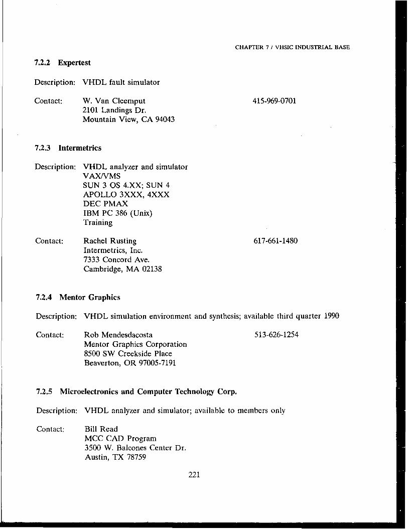
CHAPTER 7 / VHSIC INDUSTRIAL BASE
7.2.2 Expertest
Description: VHDL fault simulator
Contact: W. Van Cleemput 415-969-07012101 Landings Dr.Mountain View, CA 94043
7.2.3 Intermetrics
Description: VHDL analyzer and simulatorVAX/VMSSUN 3 OS 4.XX; SUN 4APOLLO 3XXX, 4XXXDEC PMAXIBM PC 386 (Unix)Training
Contact: Rachel Rusting 617-661-1480Intermetrics, Inc.7333 Concord Ave.Cambridge, MA 02138
7.2.4 Mentor Graphics
Description: VHDL simulation environment and synthesis; available third quarter 1990
Contact: Rob Mendesdacosta 513-626-1254Mentor Graphics Corporation8500 SW Creekside PlaceBeaverton, OR 97005-7191
7.2.5 Microelectronics and Computer Technology Corp.
Description: VHDL analyzer and simulator; available to members only
Contact: Bill ReadMCC CAD Program3500 W. Balcones Center Dr.Austin, TX 78759
221
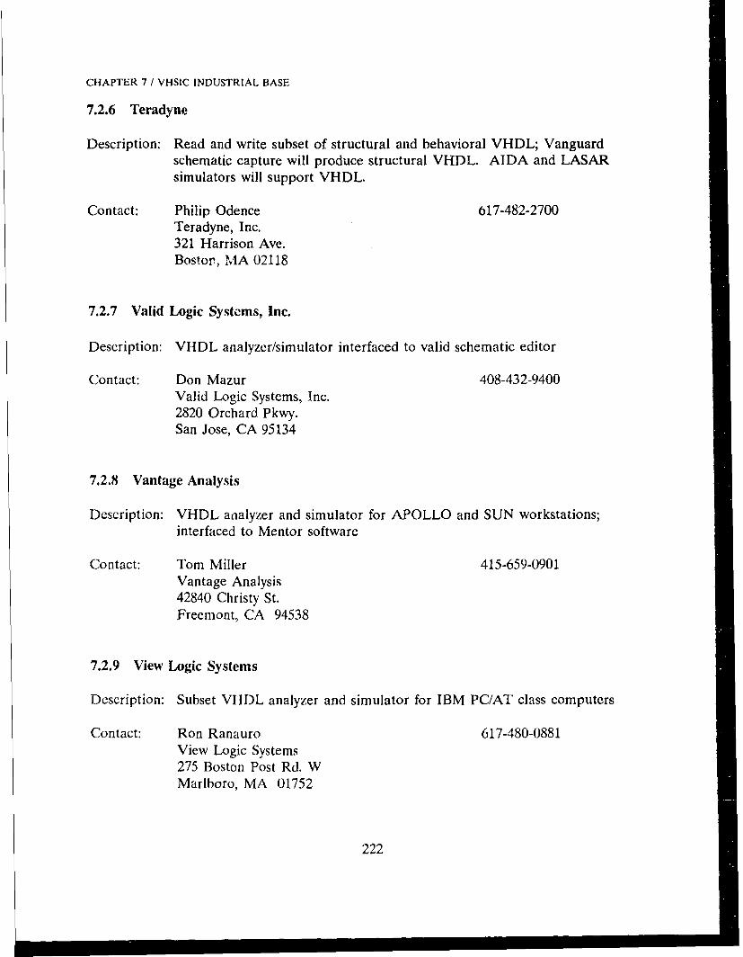
CHAPTER 7 / VHSIC INDUSTRIAL BASE
7.2.6 Teradyne
Description: Read and write subset of structural and behavioral VHDL; Vanguardschematic capture will produce structural VHDL. AIDA and LASARsimulators will support VHDL.
Contact: Philip Odence 617-482-2700Teradyne, Inc.321 Harrison Ave.Bostor, MA 02118
7.2.7 Valid Logic Systems, Inc.
Description: VHDL analyzer/simulator interfaced to valid schematic editor
Contact: Don Mazur 408-432-9400Valid Logic Systems, Inc.2820 Orchard Pkwy.San Jose, CA 95134
7.2.8 Vantage Analysis
Description: VHDL analyzer and simulator for APOLLO and SUN workstations;interfaced to Mentor software
Contact: Tom Miller 415-659-0901Vantage Analysis42840 Christy St.Freemont, CA 94538
7.2.9 View Logic Systems
Description: Subset VHDL analyzer and simulator for IBM PC/AT class computers
Contact: Ron Ranauro 617-480-0881View Logic Systems275 Boston Post Rd. WMarlboro, MA 01752
222
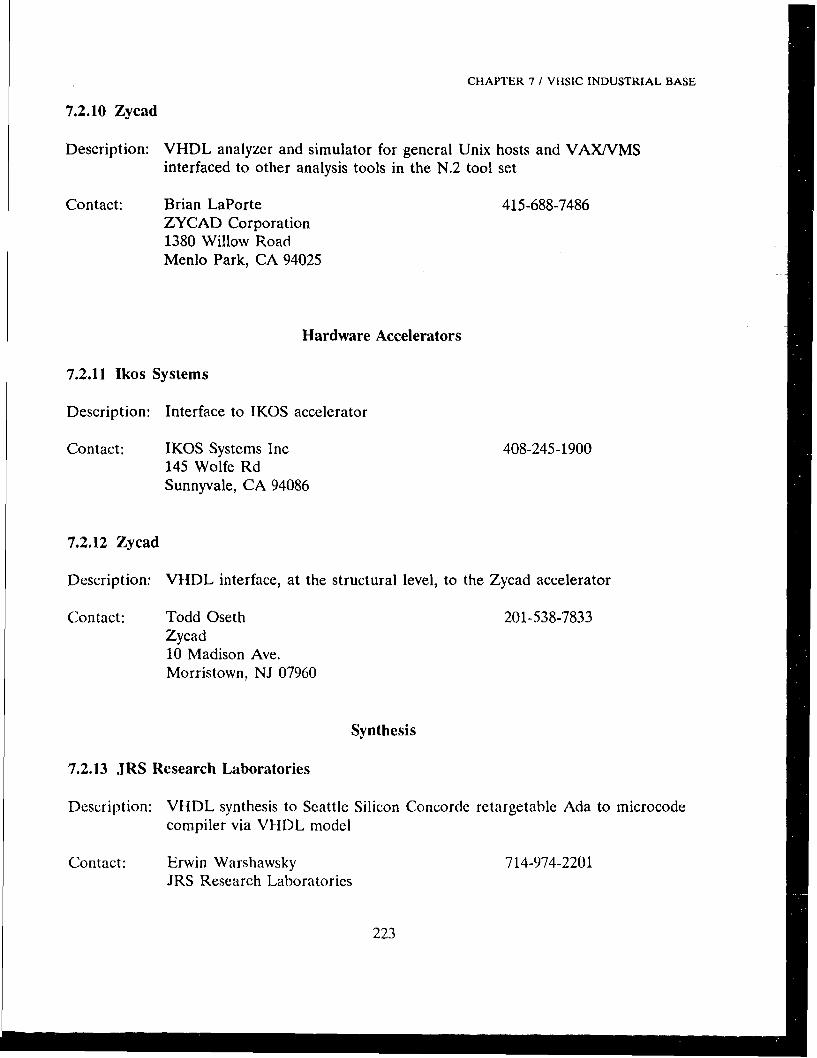
CHAPTER 7 / VHSIC INDUSTRIAL BASE
7.2.10 Zycad
Description: VHDL analyzer and simulator for general Unix hosts and VAXNMSinterfaced to other analysis tools in the N.2 tool set
Contact: Brian LaPorte 415-688-7486ZYCAD Corporation1380 Willow RoadMenlo Park, CA 94025
Hardware Accelerators
7.2.11 Ikos Systems
Description: Interface to IKOS accelerator
Contact: IKOS Systems Inc 408-245-1900145 Wolfe RdSunnyvale, CA 94086
7.2.12 Zycad
Description: VHDL interface, at the structural level, to the Zycad accelerator
Contact: Todd Oseth 201-538-7833Zycad10 Madison Ave.Morristown, NJ 07960
Synthesis
7.2.13 JRS Research Laboratories
Description: VHDL synthesis to Seattle Silicon Concorde retargetable Ada to microcodecompiler via VHIDL model
Contact: Erwin Warshawsky 714-974-2201JRS Research Laboratories
223
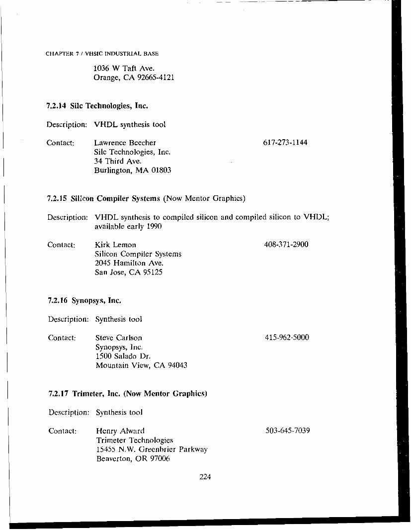
CHAPTER 7 / VHSIC INDUSTRIAL BASE
1036 W Taft Ave.Orange, CA 92665-4121
7.2.14 SUc Technologies, Inc.
Description: VHDL synthesis tool
Contact: Lawrence Beecher 617-273-1144Silc Technologies, Inc.34 Third Ave.Burlington, MA 01803
7.2.15 Silicon Compiler Systems (Now Mentor Graphics)
Description: VHDL synthesis to compiled silicon and compiled silicon to VHDL;available early 1990
Contact: Kirk Lemon 408-371-2900Silicon Compiler Systems2045 Hamilton Ave.San Jose, CA 95125
7.2.16 Synopsys, Inc.
Description: Synthesis tool
Contact: Steve Carlson 415-962-5000Synopsys, Inc.1500 Salado Dr.Mountain View, CA 94043
7.2.17 Trimeter, Inc. (Now Mentor Graphics)
Description: Synthesis tool
Contact: Henry Alward 503-645-7039Trimeter Technologies1545b N.W. Greenbrier ParkwayBeaverton, OR 97006
224
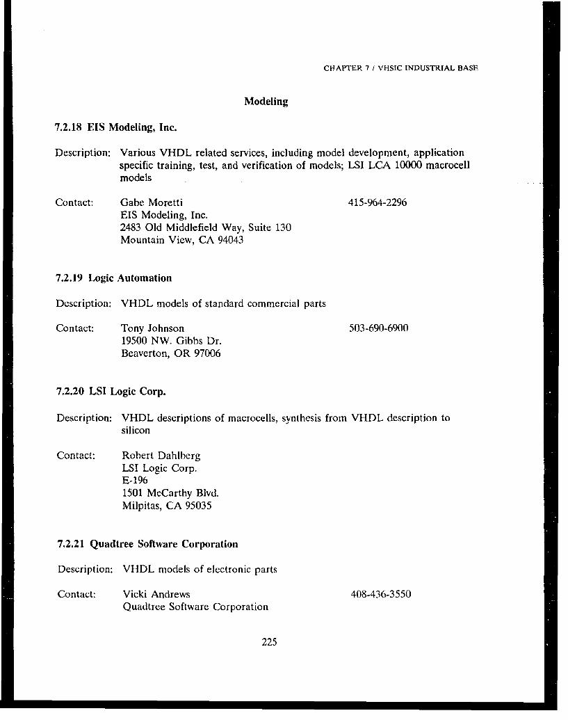
CH4APTER 7 / VHSIC INDUSTRIAL BASE
Modeling
7.2.18 EIS Modeling, Inc.
Description: Various VHDL related services, including model development, applicationspecific training, test, and verification of models; LSI LCA 10000 macrocellmodels
Contact: Gabe Moretti 415-964-2296EIS Modeling, Inc.2483 Old Middlefield Way, Suite 130Mountain View, CA 94043
7.2.19 Logic Automation
Description: VHDL models of standard commercial parts
Contact: Tony Johnson 503-690-690019500 NW. Gibbs Dr.Beaverton, OR 97006
7.2.20 LSI Logic Corp.
Description: VHDL descriptions of macrocells, synthesis from VHDL description tosilicon
Contact: Robert DahlbergLSI Logic Corp.E-1961501 McCarthy Blvd.Milpitas, CA 95035
7.2.21 Quadtree Software Corporation
Description: VHDL models of electronic parts
Contact: Vicki Andrews 408-436-3550Quadtree Software Corporation
225
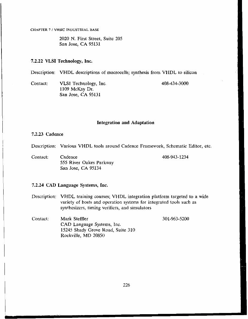
CHAPTER 7 / VHSIC INDUSTRIAL. BASE
2020 N. First Street, Suite 205San Jose, CA 95131
7.2.22 VLSI Technology, Inc.
Description: VHDL descriptions of macrocells; synthesis from VHDL to silicon
Contact: VLSI Technology, Inc. 408-434-30001109 McKay Dr.San Jose, CA 95131
Integration and Adaptation
7.2.23 Cadence
Description: Various VHDL tools around Cadence Framework, Schematic Editor, etc.
Contact: Cadence 408-943-1234555 River Oakes ParkwaySan Jose, CA 95134
7.2.24 CAD Language Systems, Inc.
Description: VHDL training courses; VHDL integration platform targeted to a widevariety of hosts and operation systems for integrated tools such assynthesizers, timing verifiers, and simulators
Contact: Mark Steffler 301-963-5200CAD Language Systems, Inc.15245 Shady Grove Road, Suite 310Rockville, MD 20850
226
Ml
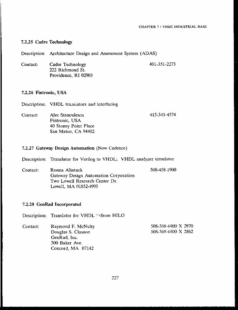
CHAPTER 7 / VHSIC INDUSTRIAL BASE
7.2.25 Cadre Technology
Description: Architecture Design and Assessment System (ADAS)
Contact: Cadre Technology 401-351-2273222 Richmond St.Providence, RI 02903
7.2.26 Fintronic, USA
Description: VHDL traasiators and interfacing
Contact: Alec Stanculescu 415-345-4574Fintronic, USA40 Stoney Point PlaceSan Mateo, CA 94402
7.2.27 Gateway Design Automation (Now Cadence)
Description: Translator for Verilog to VHDL; VHDL analyzer simulator
Contact: Ronna Alintuck 508-458-1900Gateway Design Automation CorporationTwo Lowell Research Center Dr-Lowell, MA 01852-4995
7.2.28 GenRad Incorporated
Description: Translator for VHDL "-/from HILO
Contact: Raymond F. McNulty 508-369-4400 X 2970Douglas S. Clauson 508-369-4400 X 2862GenRad, Inc.300 Baker Ave.Concord, MA 07142
227
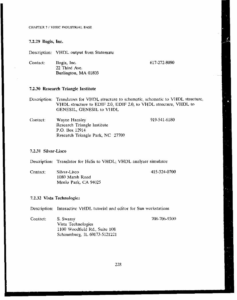
CHAPTER 7 / VHSIC INDUSTRIAL BASE
7.2.29 Ilogix, Inc.
Description: VHDL output from Staternate
Contact: Ilogix, Inc. 617-272-809022 Third Ave.Burlington, MA 01803
7.2.30 Research Triangle Institute
Description: Translators for VHDL structure to schematic, schematic to VH-IDL structure,VHDL structure to EDIF 2.0, EDIF 2.0, to VHDL structure, VHDL toGENESIL, GENESIL to VHDL
Contact: Wayne Hansley 919-541-6180Research Triangle InstituteP.O. Box 12914Research Triangle Park, NC 27709
7.2.31 Silvar-Lisco
Description: Translator for Helix to VHDL; VHDL analyzer simulator
Contact: Silvar-Lisco 415-324-07001080 Marsh RoadMenlo Park, CA 94025
7.2.32 Vista Technologies
Description: Interactive VHDL tutorial and editor for Sun workstations
Contact: S. Swamy 708-706-9300Vista Technologies1100 Woodfield Rd., Suite 108Schaumburg, IL 60173-5121221
228

ACKNOWLEDGEMENTS
Great appreciation is extended to tile many DoD personnel who, over the more than te-nyeatrs of VI-SIC activity, have participated in the program reviews, provided valuable adviceand technical guidance both to thle program offices anid to the contractors, and who have spentmany hours helping to formulate the program plans, the RFPs, the technical guidancedocuments, and the innumerable other technical tasks that have gone- into the running of thlislarge, complex, and dynamic prograrn. Thle technical managers were immeasurably helped byable assistance from contracting officers and budget specialists. Without the enthusiasticparticination and dedicated efforts of all of the technical and administrative people, theVIISIC Program would not have been possible. The program directors and their principalas.-istants are listed below.
VH'IiC Program IDirectors/Managers (1980) - 1990)
DOD1 Ariny A F Navy NASA
L, W. Suminey C. (3. Thornton W. J. Edwards N. Butler 11, iBenzE. 1). Maynard, Jr. P1. 11 ud-son .1. M. Blasingamne E. 1D. CohenJ. M. MacCalluni 11. Borkaii R. M. Werner P. Gariano, Jr.L. Cohn (D)NA) R. 11I. Sproat J. 1). Letellier
Contributors to the VHSIC1 Final Report
Tlhe VI ISIC Program Office expresses its appreciation to all the people in tliei three Servicesand to thle contractors Wh10 LOntrjhute(d to this final report on thle programi. They have spenitmany thoughtful and skillful hours gathering, selecting, writing up, arid editing the material.IThe nameis of thle principal contributors are listed below.
IDol) Report Contractors Invitud Contributors
S. I . 'lUrnbach HI. A. Alperin (Vela Associates) 11. A. Cloud (U. of Maryland)E, C.. Urban A. Brodzinsky (Vela Associates) R. 1-1. Estrada (IBMN)
1). 1. Gordon (Vela Associates) R. El. llarr (CAl))J. H ower (E-agle Research) C. S, Meyer (,Motorola)J. Recine (Analytics) R. M. Rolfe (IDA)
J. M. Schoen (MITRE)J1. 1). Stuelpimgel (West inghlo us)L. W. Suminey (SRC)L. R. Weisberg (I loncywell)
229

Contributors (continued)
Army vy Air Force
A. Bramble J. Holtkamp W. DebanyK. Chan P. Hunter H. DessaultC. F. Cook, Jr. I. Lagnado T. GlumR. V. Gar,,er J. P. Letellier M. GorniakJ. Key G. Perseghin F. G. Hall0. Layden P. Reimel R. HerndonS. Lee D. Rooney J. HinesA. V. Lukosevicius T. Singleton D. LewallenJ. McGarrity R. Woodruff F. LongP. McHugh G. Woodward P. ManoR. Mitchell D. MaysV. Organic C. MessengerT. J. Peacher D. RichardsL. Simon W. RussellT. Tippit F. SchmandtG. Tomlin P. SpeicherS. Waldman 13. SpinkD. Woo R. StegmaierL. L. Yung J. Stauss
N. Taylor
This report was prepared by Vela Associalcs under contract N00039-89-C-0132, with theguidance of Dr. Susan E. Turnbach of the VIISIC Program Office, Palisades Institute forResearch Services produced and distributed the report,
230
APPENDIX A - REFERENCES
CHAPTER 2: HISTORY, STRUCI'URE, AND POLICIES
2.1 General Electric VHSIC Program Definition (Phase 0) Final Technical Report,03/07/80-12/12/80, Contract DAAK20-80-C-0255
2.2 Honeywell VIISIC Program Definition (Phase G) Final Technical Report, 03/15/80-12/15/80,Contract F33615-80-C-1124, DTIC No. AD-B065-779
3.3 Hughes VHSIC Program Definition (Phase 0) Final Technical Report, 03/01/80-12/01/80,Contract DAAK20-80-C-0256
2.4 IBM VHSIC Program Definition (Phase 0) Final Tcchnical Report, 09/09/80-01/09/81, Con.ractN00039-80-C-0284
2.5 Raytheon VHSIC Program Definition (Phase 0) Final Technical Report, 03/15/80-01/15/81,Contract F33615-79-C-1853, DTIC No. AD-B062-876
2.6 Rockwell VHSIC Program Definition (Phase 0) Final Technical Report, 04/07/80-03/31/81,Conlract DAAK20-80-C-0257
2.7 Texas Instruments VHSIC Program Definition (Phase 0) Final Technical Report, 03/15/80.12/05/80, Contract F33615-80-C-1123
2.8 TRW VHSIC Program Definition (Phase 0) Final Technical Report, 03/01/80-04/01/81, ContractN(XKX39-80-C-0282
2.9 Westinghouse VHSIC Program Definition (Phase 0) Final Technica! Report, 03/01/804-06/01/81,Cxontract N00039-80-C-0283
2.10 "Phase 1 Statement of Work", Appendix IV of VHSIC Annual Report for 1986j, VHSICProgram Office, Office of the Undersecretary of Defense for Acquisition, December 31. 1986,DTIC No. AD-A191-027
2.11 Honeywell VIISIC Phase 1 Final Technical Report, Contract F33615-81-C-1527, July 198(,DTIC No. AD-B133-153
2.12 Hughes VHSIC Phase I Final Technical Report, Contract i)AAK20-81-C-0383, January 1988,DTIC No. AD-13120-943
2.13 IBM VHSIC Phase I Final Technical Report, Contract N00039-81-C-0416, May 1984, rYJ'ICNo. AD-B091-279
2.14 Texas Instruments VHSIC Phase 1 and VIISIC Yield Enhancement Final 'lechnical F.eport,(Contract DAAK20-81 -C-0382, May 1988, DTIC No. AD-B132-706
2.15 Westinghouse Phase 1 VHSIC Final Teclnical Report, Contract F33615-81-C-i532, May 1989,DTIC No. AD-B132-991
231
APPENDIX A / REFERENCES
2.16 AT&T VHSIC Submicrometcr Program Definition (Phase 0') Final Technical Report, 08/01/8,1-02/28/84. Contract DAAK20-83-C-0415
2.17 Harris VHSIC Submicrometer Program Definition (Phase 0') Final Technical Report,08/01/83-03/01/84 Contract F33615-83-C- 1102, DTIC NO. AD-B094-298L
2.18 Honcywvell VHSIC Submicrometer Program Definition (Phase 0') Final Technical Report,08/01/83-02/28/84, Contract F33615-83-C-1 103, DTIC No. AD-B093-706,707
2.19 Hughes VHSIC Submicrometer Program Definition (Phase 0') Final Technical Report,08/01/83-01/31/84, Contract DAAK20-83-C-0414, DTIC No. AD-.B090-450L, 459
2.20 IBM VHSIC Submicrometer Program Definition (Phase 0') Final Technical Report,08/01/83-02/28/84, Contract N0(X)39-C-83-(X038
2.21 RCA VHSIC Submicrometcr Program Definition (Phase 0') Final 'Technical Report,08/01/83-02/28/84, Contract NO(X)39-C-83-0639
2.22 Texas Instruments VHSTC Submicrometer Program Definition (Phase 0'), Final TechnicalReport, 08/01/83-02/28/84, Contract DAAK20-83-C-0413, DTIC No, AD-B089-403L
2.23 TRW VHSIC Submicrometer Program Definition (Phase 0') Final Technical Report,08/) /83-01/31/84, Contract N(YX)39-83 C-0640
2.24 Westinghouse VHSIC Submicrometer Program Definition (Phase 0') Final Technical Report,08/01/83-02/28/84, C)ntract F33615-83-C-1104, DTIC No. AD-B094-271
2.25 VHSIC Briefs (Phase 3 Projects), May 1983, Palisades Institute for Research Services, ContractN(0039-80-C-0448, DTIC No. AD-B073-845
2.26 VHSIC Bricfts (Phase 3 Projects), November 1984, Palisades Institute for Research Scrviccs,Conti act N(X)039-80-(--0448
2.27 VIiSIC Annual Report for 198-14, VI-ISIC Program Office, Office of the Undcr Secretary ofDefens'e for Aqxjiisition, December 31, 1986, D'TIC No. AD-A191-027
2.28 VHSIC Annual Report for 1987, VHSIC Program Officc. Office of the Under Secretary ofDefense for Acquisition, December 31, 1987, DTIC No. AD-A199-880
2.29 VHSIC Annual R.cport for 1988,; VHSIC Program Officc. Office of the Under Secretary ofDelcn;e for Acquisition. Deccmber 31, 1988, I"IIC No. AD-A223.725
2.30 VI-ISIC Annual Pcport tot 1987, ,\pcndice• A] -A4. VHSIC Programn Office, Office of theUnde'rsecrctary of DdLcnse tor Acquis;ition, DcceInleI 31, 1987. DTIIC No. AD--A199-880
2.31 DoD Standardization Program PIln. VHSIC, FSC Class 5962: Microvlectronic Circuit Devices,Fiscal Years: 88-92, As-:';Jncc Activity I)IA(F:S)
232
APPEN1I1X A / REFERENCES
CHAPTER 3: DEVELOPMEN'I T'ASKS
Section 3.1: Design
3.1 VHSIC Phase 2, Submicron 'Technology Development, lntcroperabiliht Standards, ContractDAAK20-85-C-0376, IBM (in cooperation with TRW and Honeywell), November 1988, D'TICNo.AD-A203-629
3.2 VHSIC Hardware Descriptive Language (VHDL) Development Program, Contract F33615-83-C-1(X)3, Intermetrics, Inc., Final Report D'TIC Nos. AD-B081-857 (October 1983) and AD-B132-637L (September 3988, AFWAL TR-88-1072)
3.3 Software Detailed Design Document for the ADAS/VHDL System (RTI Report), Center forDigital Systems Research, Departmcnt of the Navy, Space and Naval Warfare SystemsCommand, September 1987
3.4 Software User's Manual for the ADAS/VHDL System (R111 Report), (Center for Digital SystemsResearch, Department of the Navy, Space and Naval Warfare Systems Command, September1988
3.5 Air Force, Wright Research and Development Center, Report WRDC 'TR-89-5(X)06
3.6 Baker, Robert L. and Scheper, Charlotte 0., Image Proccssor Design Using SiliconCompilation. Presented at Generic Signal Processing Workshop, Laurel, MD, July 22-23, 1987
3.7 Clary, J. B., Design 'Tools for Real-'Tine Signal Processing Systems, San Diego, CA, August20, 1987. SPIE's 31st Annual International Technical Symposium on Optical and Opto-electronic Applied Science & Engineering.
3.8 Franke, D. L. and Hansley, K. W., ASIC Design Begins With System Design. Presented atELECIRO-88, Boston, MA, May 1988
3.9 Scheper, C.0. and Baker, R, L., VHSIC Silicon Compiling lools Applied to Image Processing,GOMAC '87, Orlando, FL, October 26-29, 1987
3.10 Software Detailed Design Document for thu VHSIC Silicon Compiler System (Report by RTI.Silicon Compiler Systems, and E-Systems), Center for Digital Systems Research, Departmentof the Air Force, WRDC EL, April 1987
3.11 Software User's Manual for the VHSIC Silicon Compiler System (Report by RTI, SiliconC)mpilcr Systems. and] E-Systems), Department of the Air Force, WRDC EL, April 1987
3.12 Augustin, L. M., Ciennart, B. A., I luh, Y., Luckham, D. C., and Stanctlcscu, A. -.. "Verificationof VHDL I)csigns Using VAL". Proceedings of the 25th ACM/IEEE Design AutomationConference, Jine 12-15,1988, Analhcim, pp. 48-53
233

APPEN1I1X A / REFERENCES
3.13 Augustin, L. M., Gennart, B. A., Huh, Y., Luckham, D. C., and Stanculescu, A. G., "AllOverview of VAL", Technical Report CSL-TR-88-367, Computer Systcms Laboratory, StanfordUniversity, October 1988
3.14 VHSIC Annotation Language (Report by Stanford University), Wright Research andDevelopment Center, Report WRDC TR-89-5047
3.15 Runner, D. and Warshawsky, E., Synthesizing Ada's Ideal Machine Mate, VLSI Systems Design,VAX, No. 10, p. 30, October 1988
3.16 Warshawsky, E., et. al., Integrated Design Automation and Artificial Intelligence, Proceedingsof Aerospace Applications of Artificial Intelligence Conference, AAAI( 88, Dayton, OH,October 24-28, 1988
3.17 Prakash, S. and Parker, A., Specification of Timing Constraints for Digital Hardware, Submittedto Ninth International Symposium on Computer Hardware Description Languages and theirApplications, Washington, DC, June 1989
3.18 Jain, R., Parker, A. C. and Park, N., Module Selection for Pipclined Designs. Proceedings of25th Design Automation Conferencc, ACM/IEEE, June 1988
3.19 Jain, R. and Parker, A. C., Design Style Selection in Digital Systems. Proceedings ofTECHCON '88, Semiconductor Research Corporation, October 1988
3,20 Jain, R., Mlinar, M. J., and Parker, A. C., Area-Time Model for Synthcsis of Non-PipclincdDesigns. Proceedings of International Conference on Computer-Aided-Design, ACM/IEEE,November 1988
3.21 Parker, A. C., Hayati, S., Jain, R., Kucukcakar, K., Mlinar, M. J., Prakash, S. and Seidel, J.,High-Level Synthesis in the ADAM System. Proceedings of Second International Workshopon VLSI Design, Computcr Society of India, India, December 1988
3.22 Jain, R., Kucukcakar, K., Mlinar, M. J., and Parker, A. C.. Experience with the ADAM SynthesisSystem. Submitted to the 26th Design Automation Conference, ACM/IEEE, June 1989
3.23 Kucukcakar, Kayhan and Parker, Alice C., "MABAL: A Software Package for Module and BusAllocation", Department of Elcctrical Engineering -- Systems, University of Southern California,submitted to Design Automation Conference 1989
3.24 Drummond, R. R. and G)gan, Major K. J. "Test Engineer's Assistant," Army Research,Development & Acquisition Bulletin, pp.11-13, Headquarters Department of the Army,July-August 1988
3.25 Hallenbeck, J. J., Kanopoulos, N., Vasanthavada, N., and Watterson, J. W,, CAD Tools forSupporting System Design for "I'cstwibility, (Generic Signal Processing Woikship, Laurel, MD,July 22-23, 1987
3.26 Kanopoulos, Nick, Hallcnebck, Jill J., Vasanthavada, Nagcsh, Watterson, J. W., CAD ToolsSupporting System Design tor Maintainability, ATE & Instrumentation Conference East, 1988
234
APPENDIX A / REFERENCES
3.27 Hallenbeck, J. J., Kanopoulos, N., Vasanthavada, N., and Watterson, J. W., CAD Tools forSupporting System Design for Testability, 1988 International Test Conference
3.28 Software Design Document for the Test Engineer's Assistant System (RTI Report), Center forDigital Systems Research, Department of the Army, LABCOM ETDL, August 18, 1988
3.29 Software System User's Manual for the Test Engineer's Assistant System (RTI Report), Centerfor Digital Systems Research, Department of the Army, LABCOM ETDL, December 1988
3.30 Analog Design with VHDL (Dartmouth University Report), Wright Research and DevelopmentCenter, Report WRDC TR-89-5026
3.31 AIVD User's Reference Manual (Octy, Inc. Report), Center for Digital Systems Research,Department of the Army, LABCOM ETDL, December 1988
3.32 Artificial Intelligence for VHSIC Systems Design (AIVD) Specifications (Octy, Inc. Report),Center for Digital Research, Department of the Army, LABCOM ETDL, April 1988
3.33 Final Reports: EIS Specification (3 volumes), available from Honeywell, Inc., 3660 TechnologyDrive, Minneapolis, MN 55418
3.34 EIS User Manual available from Honeywell, Inc., 3660 Technology Drive, Minneapolis, MN55418
Section 3.2: Test and Life Cycle Support
3.35 Electrical Test and Evaluation of VHSIC Static RAMs, F.G. Hall and W.J. Horth, GOMACProceedings 1985, p.417, DTIC No. AD-BlOO-607
3.36 "Electromagnetic Effect Requirements for VHSIC Devices", R. V. Garver (Army HDL), R.Richardson (NSWC), and T. Baustert (AF RADC), September 1986, Harry DiamondLaboratories Report HDL-SR-86-5
3.37 "An Interchange Format for Electronic Data", W. E. Russell and M. S. Karlovic, Addendumto Proceedings 1986 Computer Standards Conference, IEEE, San Francisco, July 1986
3.38 "Tester Independent Support Software System (TISSS)", J. Falkenstrom et al, Proceedings 1985IEEE International Test Conference, pp. 685-690
3.39 "Automation for Generation and Maintenance of Microcircuit Performance Specifications forDesign and Life Cycle Support Using the Tester Independent Support Software System (TISSS)",J. Haberer, 1987 White Paper
3.40 "TISSS in the CALS Environment", J. Graffo and D. Harmon, Proceedings of the 1987 IEEEReliability and Maintainability Symposium, Philadelphia, June 1987, pp. 205-208
3.41 "A Computer-Aidcd lTest Generation System for VItSIC", M. S. Karlovic, Test MeasurementWorld, $2-$9, November 1986
235
APPENDIX A / REFERENCES
3.42 Reliability Reassessment of Gate Arrays, General Telephone and Electronics, Final Report,Contract F30602-86-C-0176, Report RADC TR-89-275
3.43 Reliability Prediction Modeling, IITRI and Honeywell, Contract F30602-86-C-0261, ReportRADC-TR-89-177, October 1989, DTIC No. AD-A-214-601
3.44 Maintenance Concepts for VHSIC, Honeywell Contract F30602-85-C-0091, Final Report,RADC-TR-87-13, July 1987, DTIC No. AD-B-119-216
Section 3.3: Chip Fabrication
3.45 WIM VHSIC Phase 2 Submicron Technology Development Final Technical Report, ContractDAAK20-85-C-0376, September 1989, Report SLCET-TR-85-0376-F, DTIC No. pending
3.46 R.C. Zittel, M. Simons, H.L. Hughes, D.G. Platteter, "Radiation Hardness of VHSIC Phase ITechnologies", Digest of Papers, Vol. XI, GOMAC 1985, DTIC No. AD-B100-607
3.47 M.D. Jacunski, F.C. Blaha, W.L. Jacksoni, J.R. Cricchi, "A Radiation Hardened 10K Gate Arrayfor Space Applications", Digest of Papers, Vol. XIV. GOMA(" 1988, DTIC No. AD-B129-239
3.48 R.J. Brzozowy, "An S-Lcvel Radiation-Hardened Gate Array with Build-In Self Test andMaintenance Capability", Digest of Papers, Vol. XIII, GOMAC 1987, .DTIC No. AD-B119-187
3.49 C.E. Schlier and L.R. Rockett, "VHSIC Radiation Hardening Program Extension-to-SpaceLevcls", Technical Reports DNA-TR-85-356, Aug. 1985, and DNA TR-87-53, January 1987.
3.50 K.G. Aubuchon, "VHSIC Phase 1 Extension-to-Space"'Technical Report DNA-TR-87-187, July1987.
3.51 D. Berndt and R. Belt, "Honeywell Single-Event Upset Test Chip Advanced Digital BipolarIII VHSIC I Technology", Technical Report DNA-TR-87-270, September 1987.
3.52 J.S. Cable and B.L. Hikin, "VHISC Latchup Elimination Program", Technical Report DNA-"1'R-88-32, March 1988.
3.53 B.L. Keeney and J.F. Salzman, "Phase II, DNA Bipolar Dose Rate Hardening", TechnicalReport DNA-TR-88-226, August 1988.
3.54 Hughes/Perkin-Elmer, "Electron Beam Lithographic Equipment" (VHSIC Phase 1), ContractDAAK20-81-C-0384, Final Technical Report for period 5/1/81-4-31-86, Report DELET TR-81-C-0384-4, DTIC No. Pending.
3.55 A.M. Carroll and J.L. Freyer, "Measuring the Performance of the AEBLE 150 Direct-Write-E-Beam Lithography Equipment", Proceedings of the SPIE Microlithography IV Conference,Santa Clara, CA, March 1985.
3.56 J.L. Freycr and R.M. Sills, "AEBLE 150 Performance in a Mix and Match Environment",Proceedings of the SPIE Microlithography IV Conference, Santa Clara, CA, p. 5, March 1985.
236
APPENDIX A / REFERENCES
3.57 Hughes Research Laboratory, "VHSIC Electron Beam Lithography Components for DirectlyWriting Very High Speed Integratcd Circuits", Contract DAAK20 80-C-0262, Final TechnicalReport No. DELET-TR-80-0262-F, DTIC No. AD-B094-565L
3.58 TRW/GCA (VHSIC Phase 3) "Soft-ware for Electron Beam Lithography", ContractDAAK20-81-C-0263, Final Technical Report, for period 09/01/80-01/04/82, Report DELETTR-80-C-0263, Vols. I and 2, DTIC Nos. AD-13078-420 and AD-B078-421
3.59 Perkin-Elmer "Proposal to Extend Microlithography Technology", Contract DAAK20-89-C-0261, Report No. DELETE-TR-80-0261-3, DTIC No. AD-B074-215
3.60 W.D. Buckley and G.P. Hughes, "An X-ray Lithography System", J. Electrochem. Soc. 128 (5)1106, (May 1981)
3.61 "GCA Half-Micron Deep UV Stepper System Accepted at VHSIC Phase 2 Contractor's Facilityby DOD", E.J. Sweeney, R. Seltzer, GCA, General Press Release, Randover, CA, June 1988
3.62 "Practical Half-Micron Lithography With a 1OX KrF Excimer Laser Stepper", R.L. Woo, C.F.Lyons, R.M. Mueller, J.F. Conway, IBM, KTI Interface 1988 Microelectronics Seminar,Sunnyvale, CA, November 11, 1988
3.63 "Characterization and Process Control of Thermally Activated Resists". S. Das, J. Gaw, and R.Hollman, Intel, International Photopolymcrs Conference, San Diego, CA, October 30, 1988
3.64 "Process Control in the Application of Desire to Deep UV Lithography," S. Das, J. Gaw, andR. Hollman, Intel, KTI Microelectronics Seminar, Santa, Clara, CA, November 10-11, 1988
3.65 "Deep UV ANR Photoresists for 248nm Excimer Laser Plotolithography", J.W. Thackeray,G.W. Orsula, E.K. Pavelchck, D. Canistro (Shipley Co).) L.E. Bogan, A.K. Berry, K.A. Grazian(Rhom and Haas), Shipley and Rohm & Haas, SPIE Conference/Microlithography, Santa Clara,CA, February 26-March 3, 1989
3.66 "A Resist Strategy for Deep-UV Lithography", K.J. Orvek, C. Garza, R. Doering, TexasInstruments, SPIE 1989 Conference, Santa Clara, CA, March 1989
3.67 "Deep UV ANR Photoresists for 248nm Excimer Laser Photolithography," J.W. Thackeray,G.W. Orsula, E.K. Pavelchek, D. Canistro (Shipley Co.), L.E. Bogan, A.K. Berry, K.A. Graziano(Rohm and Haas), Shipley and Rohm & Haas, SPIE Conference/Microlithography, San Diego,CA, August 6-11, 1989
3.68 Laser Pantography, Final Report for the Very-High-Specd Integrated Circuits ProgramLawrence Livermore National Laboratory Report - UCRL-53878-89.
3.69 Multichip Packaging Technology with Laser-Patterned Interconnects, A.T. Barfknecht, D.B.Tuckerman, J.L. Kashmiter, and B.M. McWilliams, IEEE Trans. Comp., Hybrids, ManufacturingTechnology, vol. CHMT-12, no.4, pp. 646-649. 1989
237
APPENDIX A / REFERENCES
3.70 Vacuum Die Attach for Integrated Circuits, E.H. Schmitt and D.B. Tuckerman, Pending U.S.Patent Application Serial No. 07/243,536
3.71 Thin Film Chip-to-Substrate Interconnect and Methods for Making Same, D.B. Tuckerman,Pending U.S. Patent Application Serial No. 07/202,296
3.72 Laser-Patterned Interconnect for Thin-Film Hybrid Wafer-Scale Circuits D.B. Tuckerman,IEEE Electron Device Lett. (USA) vol.EDL-8, no.11, pp. 540-3 (Nov. 1987)
3.73 Demonstration of High-Performance Silicon Microchannel Heat Exchangers for Laser DiodeArray Cooling D. Mundinger. R. Beach, W. Benett, R. Solarz, W. Krupke, R. Stayer and D.B.Tuckerman, Appl. Phys. Lett. (USA) vol.53, no.12, pp. 1030-2 (19 September 1988)
3.74 RF Power Amplifier Cooling: LLNL Final Report to Air Force Systems Command, A.F.Bernhardt, N.J. Colella and R.J. Contolini Lawrence Livermore National Laboratory Report -UCID-21953
3.75 A Laser Direct Write Double-Lcvel-Metal Technology for Rapid Fabrication, C.Y. Fu, N.F.Raley, V. Malba, R. Hsu, R. Hills and C. Lai, Custom Integrated Circuits ConferenceProceedings, May 1990, in press.
3.76 Hewlett-Packard (VHSIC Phase 3) "Electron Resist Materials for VHSIC", Contract DAAK20-80-C-0264, Report No. DELET-TR-80-0264-1, DTIC No. AD-B067-881L and Report No.DELET-TR-80-0264, DTIC No. AD-B067-880L
3.77 "Electron Resist Materials for Very High Speed Integrated Circuits", Ha Choong and F.J. Kahn,J. Vac. Tech. Soc., 19(4), 1121 (1981)
3.78 Electronic Packaging for VHSIC, Final Report, DELET-TR-80-0267F
3.79 Improved Performance Package for VHSIC, Final Report, AFWAL-TR-83-4183
3.80 Tcchnical Guidelines for LSI Hybrid Microcircuits, Final Report, June 1984, DELET-TR-80-0302
3.81 High Density - High Pcrformancc Hybrid Circuit Technology, Final Report, August, 1983,
AFWAL-TR-82-1087
3.82 Hermetic Chip Carrier Compatible PWB Final Report, AFWAL-TR-85-4082
3.83 High Density Multilayer Package Development, Final Report, Hughes Aircraft, 1986
3.84 High Density Multi-layer Package Development, Final Report, Martin Marietta, 1986
3.85 High Density Multilayer Package Development, Final Report, Honeywell, 1986
3.86 "High Density Multilayer Pin (Grid Array Package Development", R. Spielberger, GOMAC1985 Digest of Papers, Session 22, DTIC No. AD-B100-607
3.87 VHSIC Low Dielectric Constant Printed Wiring Boards, AFWAL-TR-86-4141, February, 1987
2-38
APPENDIX A I REFERENCES
3.88 "Development of Low Diclcctric Laminate Materials for Printed Wiring Boards", 19th Int.SAMPE Tech. Conf., Vol. II, pp. 187-198, October 1987
3.89 Manufacturing Methods and Techniques for VHSIC Multichip Packages, Texas Instruments,] (89
3.90 VHSIC Multichip Microcircuit Technology Program, Teledyne, Final Report, NOSC TD 1724
3.91 TAB Manufacturing Methods and Techniques, Final Report, Honeywell, 1987
3.92 Non Destructive Evaluation of Metallized Tape Bonds Formed by Tape Automatic Bonding,Final Report, Sonoscan, 1989
3.93 "Honeywell VHSIC Phase 2 Packaging Technology", C. J. Speerschneidcr et al, 1987 VHSICPackaging Conference Proceedings, April 22, 1987
3.94 "Characteristics of Polymide Material for Use in Hermetic Packaging", R.J.Jensen, et al, 1987VHSIC Packaging Conference Proceedings, April 22,1987
3.95 TRW VHSIC Phase 2 Interim Technical Report #3, February 1986, Contract N00039-84-C-0111
3.96 "Connectorless High Speed Interconnect", GOMAC 1987 Digest of Papers, DTIC No. AD-
B119-187
3.97 See pages 3-97 through 3-142 of Reference 3.1.
Section 3.4: Chip Descriptions
3.98 TRW VHSIC Phase I Interim Technical Report #2, 11/03/81-05/03/82, ContractN(XX)39-81-C-0414, DTIC No. AD-B{69-021
3.99 Honeywell Phase 2 Submicron Technology Final Technical Report, Contract F33615-84-C-1500,(in preparation)
3.100 "VHSIC Submicron Technology (Volume 1)", October 1989, (TRW document)
CHAPTER 4: DEMONSTRATION OF VHSIC TECHNOLOGY
4.1 VHSIC Insertion into PJH, System Design Study, Final Report, Hughes Aircraft Company,Fullcrton, CA, March 1985, Contract DAAB(7-84-C-K588
4.2 VIHSIC Insertion into EPLRS, Breadboard/Brassboard Development Model, Final TechnicalReport, Hughes Aircraft Company, Fullerton, CA, January 1990, Contract DAAB07-84-C-K588,CDRL-Jt)02-001I-ACN-1566
239
APPENDIX A / REFERENCLS
4.3 TRW VHSIC Phasc I Interim Technical Report #6, for pcriod 12/01/83 - 05/30/84, ContractN00039-81-C-0414, DTIC No. AD-B087-777
4.4 TRW VHSIC Phase I Interim Technicad Report #7, for period 05/31/84 -. 10/31/84, ContractN00039-81-C-0414, DTIC No. AD-B096-737
CHAPTER 5: VHSIC TECHNOLOGY INSERTION
5.1 Defense Science Board Report of the Task Force on the VHSIC Program: "Optimal Planningand Execution of DoD VLSI Activities", February 17, 1982, Office of the Undersecretary ofDefense for Research and Engineering
5.2 VHSIC Modular Adaptive Signal Sorter (VMASS), Contract DAAB07-87-C-P040, GeneralElectric Company, Technical Report DELEW-TR-82-065-2
5.3 VHSIC Threat Association Module (VTAM), Contract DAAL01-85-C-0648, ESL. Incorporated,Technical Report AMSEL-TR-85-C-0648 (CONFIDENTIAL)
5.4 LHX Mission Computer, ARTI Program, Final Technical Report for Period December1983-July 1986, Bell/Helicopter Textron, Contract DAA.I)2-86-C-0017, USAAVSCOM"TR-86-D-16A/B
5.5 LIIX Mission Computer, ARTI Program, Final Technical Report for Period December1983-July 1986, United Technologies Corporation, Sikorsky Aircraft Division, ContractDAAJO2-86-C-0016, USAAVSCOM TR-86-D-20A/B
5.6 LHX Mission Computer, ARTI Program, Final Technical Report for Period December1983-July 1986, IBM Federal Systems Division, USAAVSCOM "I'R-86-D-22A/B
5.7 LHX Mission Computer, ARTI Program, Final Technical Report for Period December1983-July 1986, McDonnell Douglas Helicopter Company, Contract DAAJ02-86-C-9017,USAAVSCOM ".R ,%-Il- 13A/B
5.8 LHX Mission Computer, ARTI Program, Final Technical Report for Period December1983-July 1986, Bocing-Vertol Company, Contract DAAJO2-86-C-0016, USAAVSCOM"1'R-86-D-21A/B
5.9 VIHSIC Insertion into P.111, Design Plan Final Report, Hughes Aircraft Company, Fullerton,CA, June 15, 1985, Contract DAABO7-84-C-K.588, CDRL BOOI-O01A
5.10 A VI-ISIC Time Domain Algebr:ic Encoder/Decoder Chip, Technical Brochure, Hughes AircraftCompany, Fullerton, CA, June 15, 1987, Contracts DAAB07-84-C-K588 and DAAB07-82-C-J096
5.11 VHSIC Inscrtion into EPLRS, Brcadholrd/Brasshoard Development Model, Final TechnicalReport, Hughes Aircraft Company, Fullerton, CA, January 1990, Contract DAAB07-84-C-K58/>CDRL-J(Y2-001-ACN 1566
240
APPENDIX A / REFERENCES
5.12 Common-Module VHSIC Integrated System (CVIS), Final Report Westinghouse, ContractDAAA21-87-C-0281
5.13 Common-Modulc VHSIC Integrated System (CVIS), Final Report, General Dynamics, ContractDAAA21-87-C-0287
5.14 VHSIC Automatic Target Tracker for Line of Sight Missile Guidance Applications: BreadboardDemonstration Program, Tcxas Instruments, Contract DAAH01-83-C-A091, MICOM ReportRE-85-32, July 1985
5.15 VHSIC Automatic "'1arget Tracker Brassboard Demonstration Program Final Report, (inpreparation), Texas Instruments, Contracts DAAH01-85-C-1161 and MDA972-88-C-0052
5.16 Hellfire FPA/VHSIC Chip Integration, Contract DAAH)1-85-C-Al04, McDonnell Douglas,Final Technical Report, January 6, 1987
5.17 VHSIC Insertion for Hellfire Imaging IR Seeker, Co~ntract DAAH01-85-C-A138, FordAerospace, Final Technical Report, September 27, 1989
5.18 Hellfire IIR VHSIC Joint Services Seckcr (JSS), Contract DAAHOI-85-C-A118, TexasInstruments, Interim Technical Report, May 8, 1987
5.19 VHSIC Application to Army Cormmand and Control System (ACCS), Contract DAAB07-88-C-A006, TRW, Final Technical Report, April 7, 1989
5.20 Enhanced Modular Signal Processor (EMSP) with Floating Point Arithmetic Processor (FPAP),AT&T Contract N00024-81-C-7318, CDRL V-020, Report datcd October 31, 1987
5.21 EMSP FPAP VID Product Demonstration "'cst Analysis, Report of Tests Conducted onOctober 5, 1987, Naval Underwater Systems Center, DRAFT dated November 16, 1987
5.22 Generic VHSIC Spaccborne Computer, Phase II, Final Technical Report, Honeywell ContractF29601-87-C-01 18, dated JIanuary 18, 1990
5.23 TD-660 Communications Multiplexer, Contract DAAB07-.87-C-R037, Final Design Report,SLCET-TR-84-0441-1
CHAPTER 6: TECHNOLOGY TRANSF E R
6.1 "VHSIC Technology Development and Insertion into Defense Systems", P. L. Hazan (guesteditor), API Technical Review, vol. 1, no. 2, 1989. Published by the Johns Hopkins UniversityApplied Physics Laboratory, Laurel, M D
6.2 Proceedings of 1982 VIISIC Conference, National Bureau of Standaids, (aithersburg, MD,August 3-6, 1982, DTIC Nos. AD-B066-597, 598, 599, 600, 601
6.3 Proceedings of 1983 VIISIC Conference, National Bureau of Standards, Gaithcrsburg, MD,September 19-21, 1983, DTIC Nos. AD-B076-951, 952, 953, 954, 955, 956
241
APPENDIX A / REFERENCES
6.4 Proceedings of 1984 VHSIC Conference, Naval Surface Weapons Center, Silver Spring, MD,Dccember 5-7, 1984, DTIC No. AD-B088-800
6.5 Proceedings of 1985 VHSIC CAonfcrcncc, Naval Surface Weapons Center, Silver Spring, MD,December 4-6, 1985, DTIC No. AD-B098-014
6.6 Proceedings of 1986 VHSIC Conferencc, Johns Hopkins University, Applied Physics Laboratory,Laurel, MD, December 8-10, 1986, DTIC No. AD-B108-700
6.7 Procccdings of 1987 VHSIC Conferencc, Johns Hopkins University, Applied Physics Laboratory,Laurel, MD, November 17-19, 1987, DTIC No. AD-B118-900
6.8 Proceedings of 1989 VI-SIC Conference, Hyatt Orlando, Kissimmcc, FL, November 6, 1989,DTIC NO. AD-B138-260
CHAPTER 7: VHSIC INDUSTRIAL BASE
7.1 Thornton, C., What Object Oriented Designi and Cooperative R&D Can Do for the Military,Keynote Address, Proceedings of the Fall 1988 VHDL Users' Group Meeting, Redondo Beach,CA, October 1989
7.2 Groves, B., It's Business as Usual for Militatry ASICs, ASIC Teclihology and News, pp. 20-24,February 1990
242
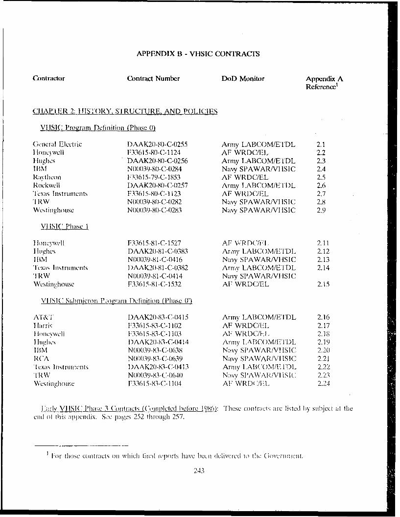
APPENDIX B - VHSIC CONTRACIS
Contractor Contra4ct Number Do.D Monitor Appendix AReferenw1
(]IAIER2: IJIS'TORY, STRUCIURE. AND POLICIES
VI ISJC'Proigramr Definition....Phasc 0)
Gciwntrl Electitic DAAK20-80-C-0255 Armiy L.ABC'OM/ETDL 2.11 IoliqweCI F3361 5-80-C-I 124 AF WRDC/EL 2.2litigihes DAAK20.-80-C-0256 Army LABCOM/E'LDL 2.3MI1NI N00039-80-C-0284 Navy SPAWAR/VI-SIC 2.4Rayvtheoll F13615-79-C-1853 AF WRDC/EL 2.5Ro ckwell DAAK20-80-C-0257 Army LABCON4/E'1DL 2.6Texas Instruments F336]5-.80-C-1 123 AF WRD(YEL 2.7'I RW N00039-80-C-()282 Navy SPAWARNIVSIC 2.8wcsti intehuse N00039-80-C-0283 Navy SPAWAR/VHS IC 2.9
VI SIC Phase I
I onvwIF33615-81-C-1527 AF WIR DC./Fl, 2.11II 11gighs DAAK20-8 1 -C-0383 Army~ LAI3COM/E1IDL 2.121IN1M N00039-8 1 -C>0416 Navy S PAWAR/VHSI C 2.13lexasý Instrunients DAAK20-81 -C-0382 Arrirv LAI3COM/E'ITDL 2.14
TRkW N00039-81 -(>0414 Navy SI'AWAR/VHSICWcstIt~OLSC F3361 5-81--C-1532 AU WRDC/E 2.15
YU SKSiC swnicron 1'Žvjgrain Defini! ioni (hase 0')
AT&'I& I)AAK20-83-C-041 i Army LABCOM/E1IDL 2.1611 lr r'k F33615-83-C-1 102 AF WRDC/F.1 2.171 loncywelli F3361.5-83-C-I 1103 AF WRDC!1-L 2.18,I Itighcs TAAK20-83-C-0414 Armiy 1.ABCOM/ETD)L 2.19I[BM N00039-83-C-0638 Naý-y SPAWAR/VIISIC 2.:2,0RCA N00039-83-C-(J639 Navy SPAWAR/'VI ISIC 2.21Te,(xas histructia.,is DAAK20-83-C-0413 Armiy LABiC(Mv/1 FDL 2,22,TkW Nt )(039-83-C-064() N.avy SPAWNA /V I S1(: 2.23WcStinli~housc F-3361 5-83-C-Il 04 Al: \VRD)"I'.'14. 2.'N
Frlv VHISIC I'asc 3 C'ontraicts -Istjtd ebe186:1hs cnrc: arc listed b y stuheco. a I the
cml) ("It thi;S ,1jppecndjx, Scc 1mves 252 throagh 257.
For those Contracts onl w'hich f,111:0 !vports have beCCrI dclvcicd ,(o thc ( overtlmnlt
24 3
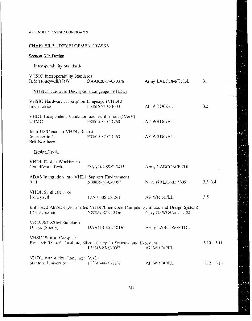
APPENDIX R3 I VHS[C CONTRACTS
CHAPTER 3: DEVELOPMENT '!ASKS
Section 3.11: Design
fntcropcrabili!ý' Standards
VHSIC hitcropcrability Standards
IBM/Honcywclltl'RW DAAK20-85-C-0376 Army LABC(.M/E fDL 3.1
VHS IC T-Iardwarc Description Lang~uage (VMi-D[L)
VI-SIC Hardware Description Language (VIIDL)I ntermctrics [33615-83-C-I 003 AF WRDCIEL 3.2
VHDL Independent Validation and Verification (PV&-V)T'1MC F330l5-85-C-11760 AF WRDC/EL
.joint tJS/C'Ina(ýian VHD I)..Pc2IostIn teriictrius/ F336 15-87-C- 1463 AF WRDC/ELBell Northern
VHII D Design Workbench1Gon IdI/Vista '1 ccli. DAALOI -85-C- 0435 Army LABCOM/Li DL
ADAS Integration into VHDL. Support EnvironmentRTI N)0039-86-C-0057 Navy NRL/Code 5305 3.3, 3.4
VIIDL Synthe;sis 1001
IdjoncyweU 173361S5-85-C-12ol AF WRD)C/EL 3.5
1L1nh,;.nced ANISDS (AuLon(IAtd VI fDI,/,iM i'CrOC.k Con IpIl)CI Sylathesis anld Desisan1 Svitemn)iR:"s Re--cai CO N01 '039-87. C-0256 Namy NSWC/Codc U-33
V1-I4DI./MIXS1N4 SimukltorTUni.-;'S (Specrrv) DAAU'I -8.5-1,-0436 Army LABCOM/ETFDL
VIASI Silicon,' COrnpilerRcscarch Tri;,ing1e Instintct, S ilicim (oni pilcr SiYs ms, and E-Systemns 3.1.0- 3.11
F33I585C-863 AF' WRD(C/EL
VA1..Annfotat~(ionL, in m!!age (VAL.)Stantor-d U'niversit ),"361.SN'6. C- 1137 AF WRDC/:J 31 31
2144
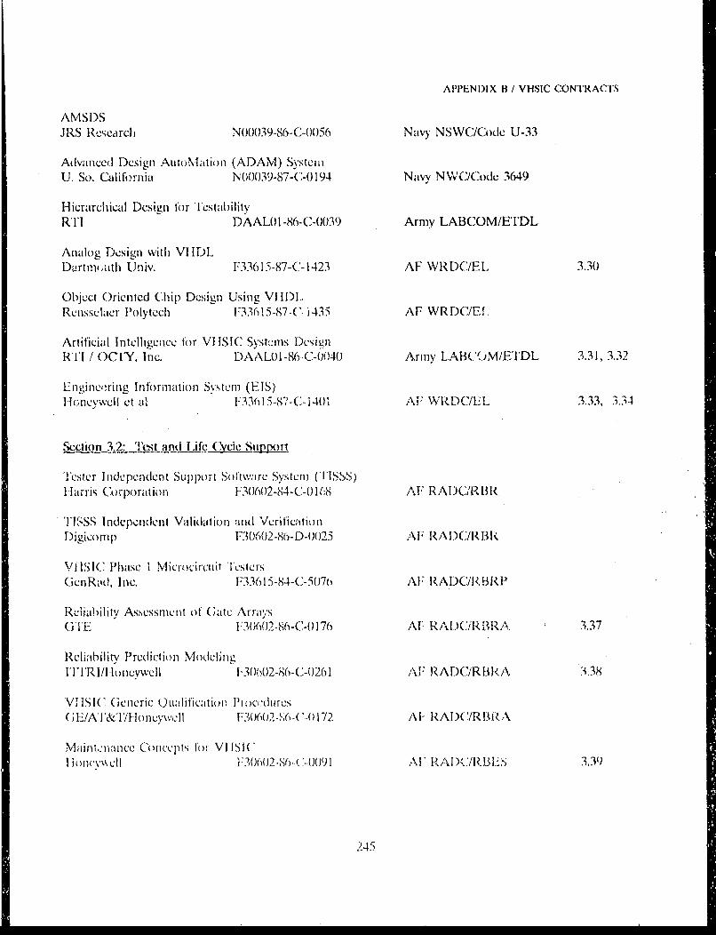
APPEND)IX B / VHSIC CONTRACTS
AMSDSJRS Resetirch N00039-86-C-0056 Navy NSWC/(:ode U-33
Advance'] Design AutoMat ion (ADAMI) SystemU. So. California N00039-87-iC,-0194 Navy NWC/Code 3649
Hicrarchical Dcsign for ~IstabilityRT1' DAALO 1 -86-C-00';9 Army LABCOM/E'IDL
Analog Design with VI IDLDa,-rtrn~uth Univ. F33615-87-C-1423 AF WRDC/EL 3.30
Object OricnIcd C 'hip Design Using Vi I)LRensselaer Polytech F33615-87-C- 1435 AF WRDC/E.I.
Artificial IntelIhgence for VI ISIC Systems DesignRil / OCUY. Inc. DAALOI-86-C-004(J Army LAB(ý-AM/EMUL 3.31, 3.32
Enrgineoring Information System (EIS)floncyvwcll ct al1-3301 5-8^,-"- 140 AF VVRDC/E*L 3.33, 3,341
S~etion 3.2: 1'(-,tandife (Qycc Sqppo~rj
"lester Inidqpendclt Support otaeSse lSSI larris Corporat ion 1:3000)2-84-C-0)168 AF R i\IC/l Il
T'11&SS I ndcpenderit Validaition and Veri ficaIti ii
Digicomp 1`30602-80-D-0025 AF RA DC/RBR-1
'i ISI(C Phase I Microcircuit Testers(jenRild, Inc. 1,336 I 5-84-C-507Th AF RADC/lBfIRP
Rcii~aility Assessmunt of Gate. ArrayvsG, IE 1:3060(2-86(C() 170 AF RADC(:R IR. .. 37
Reiahil itv Prediction N4 dei iiVITR h/1]onumwcil 130'02-86-C,-0261 AF' RADC/RIRA '.38
VHSIS ( (icneriC OLudalfictionl Pnw)CdI1resGE'/AT&TIHoneAIvwell U.30602,4;6-C-(0 172 AF RADUR/RlAi
I inl~yVell YE30002-86-G-(0) 9.1 At l¾1)C/RIU`:ý 3,31)
245
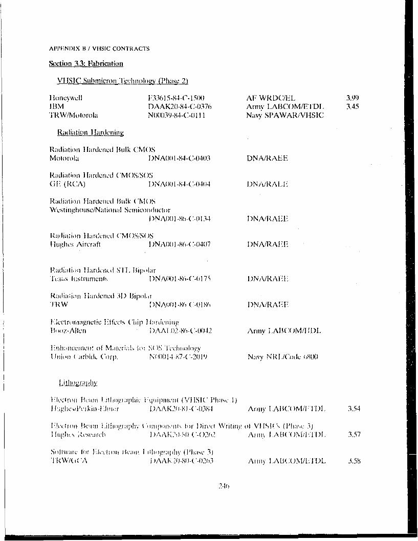
APPEND)IX B / VIISIC CONTRACTS
.Acc tion 3.3: Fabriaitioii
VI-ISIC Submicron lcchou~ Pae..
II o 11 ywcl1l F-33615-84-C- 1500 AF WRDC/EL- 3.99I HNI DAAK20-84-C-0376 Armv L-AI3C( )M/E ["IDI, 3.45I R\/Nlotorola N00039-841-C-() I I Navy SIPAWAR/VIBIIC
Radiation- 1irdnn
Radiation llrI hIrCnd Butlk CN(OSMotorola 1)NA00I-84-CA)403 DNA/kALE
Radiation I lardcm~d CMOS/ýS( )3(OF (RCA) 1 NAOU] 84(C-0-104 I)NARALI;
Radia ition Ilarocncd I BiIk ( M IOSVCst ingliolISC/Natiolula S12flicolIIctio( r
i)NAOOI -8r-( -()134 J)NA!RAE'E
PRadja~ioon I ldr(k~fludI( 4()'(II ltmdw- Aircraft 1JNA00 1 -86.('~-0407 I)N,/RAFIE
l~jalia'-ionIirdnd1)Iilr
F*lc.tro rnagnetic IFttccts ch'iip ;'Jnio
Ilti oz-Alvi Ic .A.'\i A), .86~-('-(X)02 ,\riv 1,ABCO( M/I 1)L
Unoi'on ( ;rbid. Co' rp, NN tO1 4-N'7-('-;(119 NatvyNIJ( L (OSW
II J.wh gitc&I' k-in *1 It!r wy I A A K211 *-8) -('-038.1 Army IAl()'/1 1). 3.54
Flco1 ojl 14cao )Itoim ~ r )rphr ItoI jrc Writiru, ol Vlf-I ISf (I'ha',: i)IIoi ~s~ I)A . I~)('-(V02W.Ari~IAE(()il4) 3,57
SoRw/(i( I I'A lo nB- I oh-) v!-;ihv(1-(s '0(3)A o A(N/ D
Aim) .0
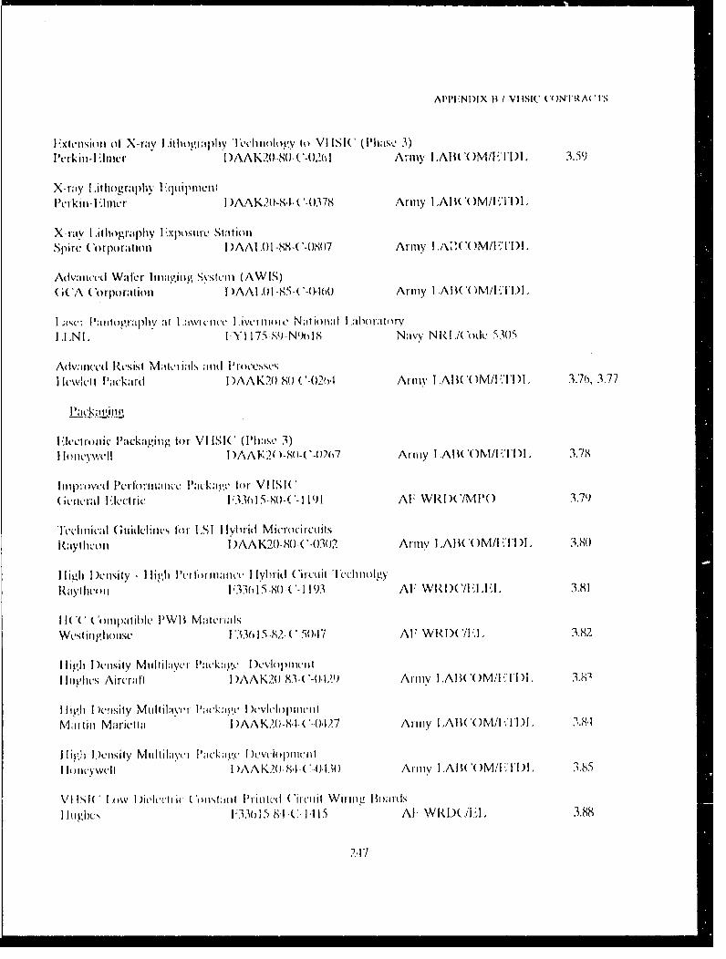
APPEIND)IX B I VI ISI(.' UNIR A('S
I"XL-cSIoll 01 X-ra'y I .itlMI;IugrIIV ICClIInoImov it) VI ISI( (PIhase 3)Pecrk I n-I 'Imer 1 )AAK20-80- C'-026~1 Army L ABCO( M/l"I'DIi) 3.59.
X-ray L ithog~rap~hy I '(W1f1pncOi
Petrkiti-1! lmcr D AAK20-84- C -0378 Army L AIB( '( )'1/~I )1
X-ray I At hograpliy I lxpr )mrc Startio~nSpirc Corporation I AAPIA -88-C -0807 Army I AC MBD
A lva iicd Watecr In igSystem (AWlS)(;( A C orporation ~ DAAi\I 1 -85-( '-01(),I Army I Al C( ( ) I IDL,
I .risc Ia1:11tOnipfhI;Iat AIWICI)CC I jVt'tI111OItc NaiflmmI I .aII1Ota!Or
1 1 N I I II 175.S89-Nor 1$ Navy NKRI.I0( bck 5305
AdIV;inccd'( RCSISt I h'il ;irIII( cscIi hwkil I i'cI'att I )AA K20-80('0e Army w l5 MI.I') 33o", 3.7 7
Elctironric P'ackaginig fin VI ISI( (Iihmsc 3)I oL'~II ) AAF.2() )-80 - ('-0?67 Armny I.Al W( )I/'I 'DI,) 3.78
I iiprowvid P1critOrnuaimcPck, fo'' r VI IS I( h';wcral FIvlcc lcI 33hI15-fX0-C '-1191 AF WRI )(YM I'( ) 3.79
Techniical ( ulitclincLs 1,0I .IIM lybrid MicmrocrrciitsRayt hconIM)AK20-80-( -0302 Army I A (()I I I. 3.80
I lag-h ki )cuily - I lighJ PCIk'nlonr:1ino JI lybri ( 'irciil T'1cchnOlrwýRaI c'iI, 3301 5-80-C- -1193 Al: WR~I )( IL'l .11 3.81
I RV ( CompIniblhl PWIý Mawcri:iksWest irghotrsc I'336 15-82-( '-50417 A I- WRI)( '/Ll. 3.82
I lit.h Denvrsity M1rltil:iVC]r l~(kIS'aka I)CVI(l]IrrwntI Itri'hics Aircra t' I ),AKI() 83(-49Army I Al C( M/"IDi,&1) 3.8-1
II igh I )CrrSity Mulflavi-rr Iackaiwc' I )MchllprirerrMalin iiiIvrieftia I )AA K?.(-84-( '-1.)47 Ar my L AI OM( )I\41I < , .1.811
II 11Y.1 D.cmirMrsIt(- ,IkIUDC ~ jII'II h(I(Y%(I DAK0 8-1MrlilyiC';ckictI,130pmn Army I .AIB('(M/1IT& 1)1 3.85
VI N'RI I 11% I )IIt'Yl- I (t- 'tir I11,i1tud ( 'iclirlit \ irin.L Boards
I~U'l). 33015-M C-1-115 Al. WRDIiOLL 3.88
2,17
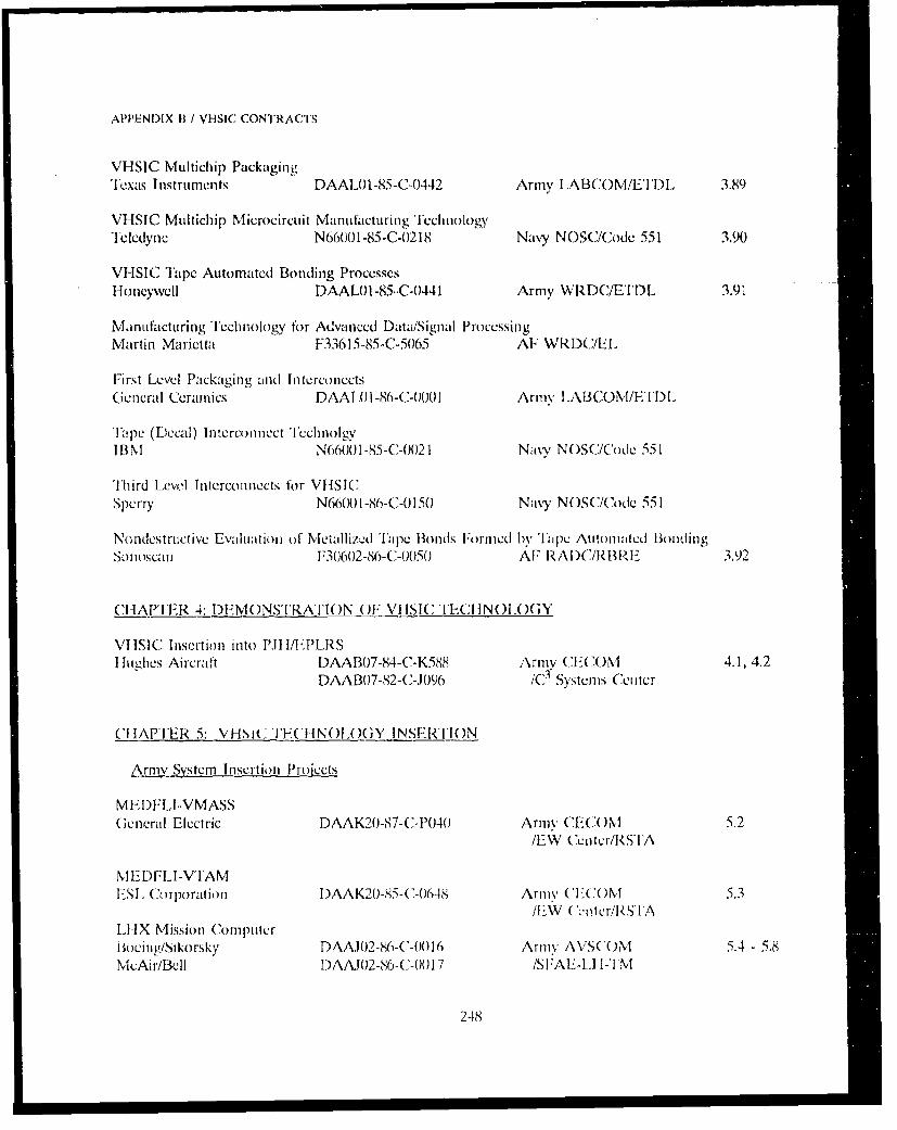
APPEND)IX B / VHSIC CONTRACTS
VHSIC Multichip PackagingTexas InstrUments DAAL()I -85-C-0442 Army I ABCOM/E'1 DL 3.89
VHISIC Multichip NI icrocircuit Matnuifacturiig 'lechniiology'Icledynec N66001 -8i-C-02 18 Navy NOSC/Code 551 3,90
VHSIC Ta-pe Automated Bonding ProccsscsH-oneywell DAAU)1-85*.C-0441 Army WRDC/E-'l'DL 3.91
Mf.inifaictuirinig Fech niology for Advanced Data/Signal ProcessingMartin Marietta F33615-85-C-5065 Al- RXYI
First Level Packaging and Interconcts(icneral Ceramics DAALOI1-86-(C-00()1 Arm%' LAI3CON/ETDL
T'[pe (DecalI) Interconnect TechnolgyI 13 T N66(J(01-85-C-002 I Navy% NOSCICode 551
T1h ird Level Intercon nects for VI S IC
Sperry N66001-86-C-0 150 Navy NOSC/Code 551I
NondestrLICtive Evaluation1 01' Metal lized Tlape Bonds Formed 1w '1apu Atitoniated B~ondingSonloscarn F30002-86-C-(J050 AF R A I)R BR E 3.92
CH-APTIER 4: DEMONSTIRATION OF VI ISIC: '1ECHNoI.( )GY
VI-SIC Insertion into T'.llI /EPLRSI ughecs Aircraft DAAB07-84-('-K588 Army ECN 4.1, 4.2
DAAB07-82-C-.J3090 K". Systems Ccu tcr
CHF APTER 5: -VI-ISiC lECHNOLOGY INSERTION
Arniv System Insertion Projects
M EDFLI-VMASSGeneral Electric DAAK20-87-C-P`040 Army ('CJI5.2
/13W Ccotcr/RSIA
MIEDFLI-V'AMl'3'1. Coiporation D)AAK20-85-C-0048 A\rmv, (T(ON'I 5.3
LHX M~ission ComputerBociniie/Sikorsky DAAJ02-86-('-0016 Armyv iVSCOM 5.4 -5.8
MicAir/Bcll DAXIO2-86-C-OO 17 IS]- AL--I- I-'I. M
248
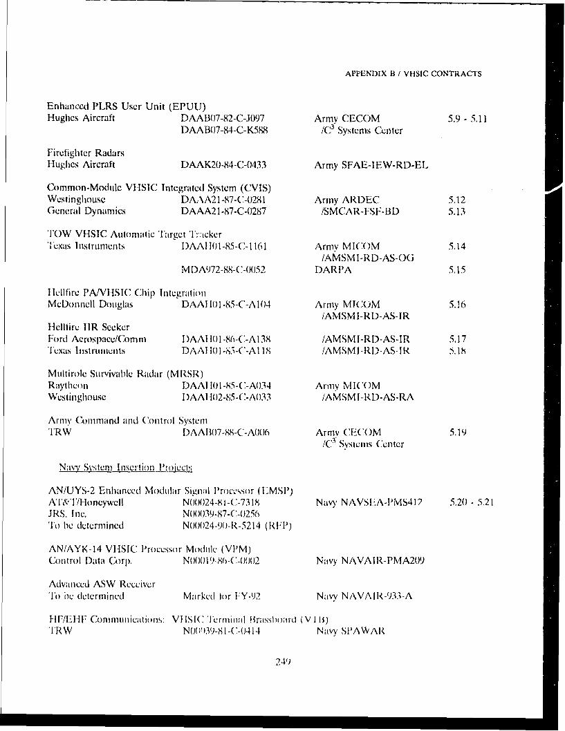
APPENDIX B / VHSIC CONTRACTS
Enhanced PLRS User Unit (EPUU)Hughes Aircraft DAAB07-82-C-J097 Army CECOM 5.9 - 5.11
DAAB07-84-C-K588 VC Systems Cen(.ter
Firefighter RadarsHughes Aircraft DAAK20-84-C-0433 Army SFAE- IEW-R D-EL
Common-ModitIc VHSIC Integrated System (C'VIS)Westinghouse DAAA2I -87-C-0291 Army ARI)EC 5.12General Dynamics DAAA21I-87-C-0287 /SMCAR-F-SF-BD 5.13
TO{W VHSIC Automatic 'Iarget 'Fr:ickcrTlexas InstrUments I)AAI 1(1-85-C,-i 161 Army MICOM 5.14
/AMSM I-RD-AS-OGM[)A972-88-C-0052 DARPA 5.15
I Iclifire PA/V VISIC.Chip IntegrationMcDonnell Dotiglas DAM 10l1-85-C-A 104 Army MICOM 5.16
iAIS-MI-RD-AS-IR1-ellfire hTR SeekerFord Aerospace/COmm DAM 10 1-86-C-Al 138 /AMSM I-RD-AS-IR 5.17*Iucxas Iiistruiiiunts DAAM 10 1-85-C-Al 18 /AMSMJ-RDI-AS-IR 5.1h
Multirole Survivable Radar (M RSRZ)Raytheon DAAI 10 1-85-C-A034 Army MI1COMWestinghouse DAM f02-85-C-A033 /AIMSM I-RI)-AS-RA
Armiy Command anid Control SystemTRW DAAI3O7-88-C-A006 Army CEC(.M 5.19
IC 37 Svstenis C*enter
Navy Systemi Insrtion I'roiec
AN/UJYS-2 Enhanced Modular Signal Processor (EMSI')A'1&'/H-oncywell N00024-8'1-C'-7318 Navy NAVSL-`A-PMS4I2 5.2(0 - 5.21J RS. Inc. N00039-87-C'-0250To tic determined N00024-90-R-521 4 (RE1:P)
AN!AYK-14 VI-ISIC' Proccssor Module (VP1M)COntrol Data (orp. NOOOI 9-80-C-0002 Navy NAVAl R-MA209
Advanccd ASW RcceiverTo ()Q (leturninred Marked tor FY-92 Navy NAVAIR-933-A
VIF/El] F Comnmunications: VI IS IC 'eriniinal lrasshard ( V I li)TRW N000~39-81I -C-04 14 Navy SPAWAk
24')
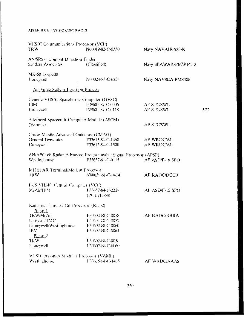
APPEND)IX B / VFHSIC CONTRACTS
VHISIC COmimunications fProcQcssor (VCP)TRW NOGO I 9-82-C-0330) Navy NAVAIR-933-K
AN/SRS- I Combat DirVc~tionl FinaderSanders -Nssociates (Chissified) Navy SPAWAR-PMW143-2
MK-5() orpcdoHioneywellI N00024-83-C-6254 Navy NAVSEA- PMS406
Air Force System Insertion) Projects
Generic VHISICSpiaccborne Computer ((;VS(')I B rvI TF296() I-87-C-f)006 AF STIC/.SWLI To nevwel F-7960 1 -87-C-() 118 AF ST'*C/SWL 5.22
Advanced SpacecrafIt Comnpu~ter Module (ASCM)(Van oiis) AF S'TCISWL
(Yusc Missile Adva Gianced il(MC (CNAG)(hnecrai Dynamics, [:336 15-84-C-1460 AF WRDC/ALI Toncywell F 33615-84-C,- 1500 AF WRDC/AL
AN/APC -68 Radar Advanced P'rogrammnable Signal Processor (APSYP)We.C-tilughoutsc [:33657-81 -(>01 115 AF ASD/F-16 SPO
MTILSF AR TIernlinal/Modleil Processor'I RW N00039-8 1 -C-04 14 AF RADC/DCCR
F-15, VI ISIC Centrol ('omlputur (VC(')MMc-rI13M 1.33657-84-C-2228 Al: ASD/F-15 SPO
(POE 7 1`358)
Radiation H ard 32-1 1ir Proccssor (101132)Plm,.c I
'I kW/McAir [30602-X-8-C-0(18 AF RADC/RBRAUniiiSvs/IJIC'( XdI
I lil\WLII\VS tI gh ti~C F30602-88-C'-(fl6(JI III F30002-88-(:-006 1
PlImse 2'IJR F 306)2-88-C-0058I Ii )i~elVAC 1 3060.)2-88-C!-0060)
VI liýIC Avioniic% MordtihitIf Pict-ssr ( VANIPI)V~cs~i~hoise 3361 5-84-('-1I4h5 AU ̀WRL)C/AAAS
2501
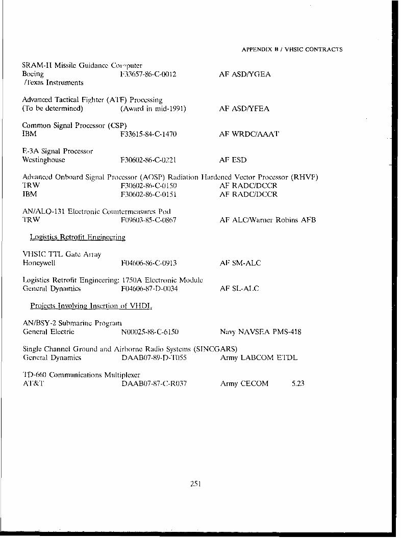
APPENDIX B / VHSIC CONTRACTS
SRAM-II Missile Guidance CowputerBoeing F33657-86-C-0012 AF ASD/YGEA/Texas Instruments
Advanced Tactical Fighter (ATF) Processing(To be determined) (Award in mid-1991) AF ASD/YFEA
Common Signal Proccssor (CSP)IBM F33615-84-C-1470 AF WRDC/AAAT
E-3A Signal ProcessorWestinghouse F30602-86-C-0221 AF ESD
Advanced Onboard Signal Processor (AOSP) Radiation Hardened Vector Processor (RHVP)TRW F30602-86-C-0150 AF RADC/DCCRIBM F30602-86-C-01551 AF RADC/DCCR
AN/ALQ-131 Electronic Countermeasures PodTRW F09603-85-C-0867 AF ALC/Warncr Robins AFB
Logistics Retrofit Enein cring
VHSIC 'ITL Gate ArrayHoneywell F04606-86-C-0913 AF SM-ALC
Logistics Retrofit Engineering: 1750A Electronic Module
General Dynamics F04606-87-D-0034 AF SL-ALC
Projects Involving Insertion of VHDL.
AN/BSY-2 Submarine ProgramGeneral Electric N00025-88-C-6150 Navy NAVSEA PMS-418
Single Channel Ground and Airborne Radio Systems (SINCGARS)Gcncral Dynamics DAAB07-89-D-'T'055 Army LABCOM ETDL
TD-660 Communications MultiplexerAT&T DAAB07-87-C-R037 Army CECOM 5.23
251

-~ N A 00 N
C'- 00 N-a-% 0' 4 '.
0 cn C N r, in) `7-
04 00 if LA Noý a' o)0 C) Co0 0:1 000 0
CA)
CA 41w > 0 4-4 -
'H0 (z 42 0C/4S-I >4 $-4I
U) 0 x C r- 0-
$L4 41 C)UP) C C 0 42
E -4 HC 41 00 0/ us 2 Hi C
A t EAi 41 C) 41
2 U(41 ( 0 42 (, ZS-
o 'Hco4
0- 0A40H 1. -,' 0" $4 'H -4
Sj ~ Cr1ý.4 ,
'H 0Z '0- Un pIo M >So 4) 00 04 Co = 4t
ý U4., "0 I w N) -4 0- '-4 - 0-4 3zbOa N. 5 5 4-'t "-J-- P'H 0 (nA 1
z- 0' .(C 41 41 > ca 0) rj> (CZ Lo 42 0CN Hj U) V)- 'H tS4 u) W1'- w -H (
0-4
S-4-4 110 0: C0 in) 04 enC-i
5-q a, -zt r-4 r'- ON CD N'0 ' i r-1 '0 '.0 04 ,-I mn U')
C) 0 1- 0l 0CDH 0
0I0n 0 0D 0 0 0 0)a 41 00 00 CC) CO C) c0 0o 00 00 00o u. I i I 1 /) 1 I
C) (C a' mn a' a' on ON 0 0mf -4 fl) -. 4 0 04 v-A 0 C) 01441 0 '.0 C> C 0r I'D '0 0ý
r. (n en 0D 0, 'n C)0/ a) 'H- ZD CD~ Zl Z i- CD4
'00
Ca) 42 ý0) 4JC/S, Pý4
-rC -, E -C (3 4-L
C- 0l 42 ob Q O4 f rI 0 " 00 ;:) W- -4 -1 co r A a - , , j (
CA .-i r- 42, Cz a) 4)2i" 10 0 r 1 :4o4 a)IC C4u: n .- ) C: )i c C u CI)42 'v- 0 ) m 0 'H A ID4 (A 4 '4J
(C ci C bO 00 r) C4 i-002 -- 4 4
252
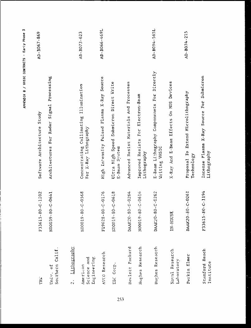
ON O U')
L0 0 C0
I.-
LIL
U)0 0 *,-j U) 4UH
0 >1 a)2S-i (1 4-3 0 co 00
Li)
0Uý ) 0D 0
z- --I C: 0aF-4 ý
:3 L oU 0 uH 1-4-3 r-l ('3 0 V) 0
co -4 .,- w 0 )(I) Cý a- U '34 00
m) E 'D CU0 U 4-4C44 -,4 CL 5 fl 4-4 CU
41i .- 1 c' -4 1/) C3 4u J-4 r-4 A 4(1 0 Ob0 'ka U) 241) U. 0J 4) 4 ~ i 4. 't(3.,A 4 (2) U) a) x- 'ýa U)L.I 4..) 0. s WH u 2U 4 C: .q "-4 V.)) U)Q ) 0~- PU
$i .H4 U4 a)) W c~ wU w 0 a>
U4 a) w-' m -AU Q) '03ý 0
u- > U r tAbL E ~0 (n bl)
4 r) c0 U; 0U (' 0 4)z. ;> 0. r_ r.0ýcý4Q)R UC a) 4-1 Q, OU Q.14.
0 ý4 0 0 -4 -4r-4' 2-H ý4 (1j) '
00 cc.0 cic 4 D '0 C9 -4O 1'0 r- _-q '.o - %0o '.o
(N .0 to) -4 %.D C14 '0 C') C14 1-4
-4 0 0 0' 0 0 C C) -4
CU C) (3 () C) C.))(
,r) 0 0ý 0ý ) 0 a. C) C0
-4 C') 1-4 C') .-4 (NI r--I Nl 0N1-
(1) 0 0D ON 00 "C") 0 0) -4 C))Z "
4-4~ Z4 (d ) Z -
u0 1!4 Ul (I .004 '3 w () Q U
vi3 U1 (n3 V'3 L) W.
a) -4 ) ()040 43V) U vi '0 41
'.w UH ~ U Uj ".--J- 'C'V T:L Lo 04-A
253

-4
~A N -4 N 4 01 -'--4 4 N'0 r-
0- 0 0r 0 0 0l 00 00 (T0
im-I
0
(2
0 0 0
0P-4 0z 4 -Ll V-4 )
aL ýXn F-4Z-4 .1i4-400
42~V 43Z) 00
0i V 0S 43 u)~ Q-4 0 ~ ~ - 0 1-/ ~ 4
E- C) 0L E- ý-X0 [ -4 0j43 4-) z:4 F-4 04- Li] F :--4 L42~ý: "-4 F-4 '- Eý 04
Q- W-~ PL rL4-4 Z~-4
r-4- 0 z 0 (42 (42 ZL F-04 V)/~Li) 04 0-- 04 Zl w 00
0 ~ 04 00 ~ WEA Zr :4-J C-)40u -
4 l) ()' 00 (Cpi C) V3) C-1 (42 00(42 c0 0 N A- 1. %D 2 L42 I' C 0 0l %
In N r-4 cfl Co ON 0) Nn4 n o'.0 0- r-4 CD CD4 '.0 tfl 00'0( C
0D C)0 0 0 C0 0 0CD o0a 00 0 0o 0o 0 00 00 w 0 o
I I4I I 1 -4 Oo D 0 0 0, 0r 0l C 0 0D 0 u -4 00 0r
(Nj (Ni re) r- 14 04 ( (N (N - -4 -11'0 CD '-0 0 ý4 0: '0 '.01' ON CD I) 0D 0 In 0 In)
-4"-4
1 0. 0) 0 0ca 0 4:I 4:1 4: 4 )4-14 U) En CA CA C) Cl)
04 (42 r) H ) r r e
0M (42 U) C/0l ..- u-I~C)Z4
254
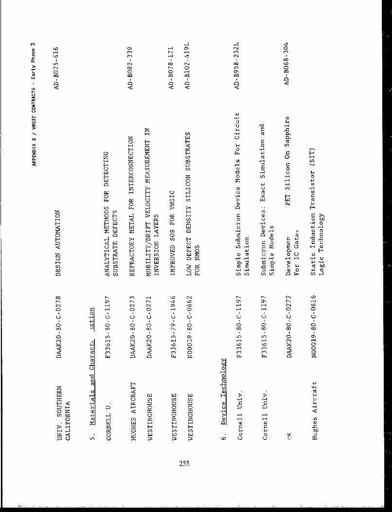
-4 en- CV)(l fCfl 4
0~00
N-0 Ca N- 0 nL 00 0 -4 0
EU
u~j I I 41
* 0 0 0 0 '
04
rxq 4-
5-i C 0
w M (ni (3)
[-4 Z 0 cn 4
0 '2 C
'W rH Z 44> Qu > U -r-4
fx) Ix 'C4 'C 'H - U 0-Cl Q) 1) Z r n '
E- z -4 4-) 4C
H u3 A- cn a) 0 U))u E- C44 'H - X r- C-
W ai) (3) .14oo 0 w 0 , 4 -, D0 4C4 ZC Lx) Hl P4V )V, :) E
00- ZO 'C % C C4 0 uOb
r4 ) Lx) H - x
HC -) 0 on H C:lC ' ) '0C
CO OH) 0o 00O 0- Lo Cf0' C* 00 4-0
H% 4 l eiI-4 r-4 HO 4' r-4 CN H
z Lx)) W) 034 00 0(3o HH) IC m 0 0n OZ04- H4 r 4 '4-4 v--i)C l P4 Lx4 41 0' 0- 4
co >b 2 .2 >- nfLx) ~ L) OZ ~ 0 'H' C' 0)0 4-wO 'Cn ~ ~-d 4-4 H (/0/) CO~t OH Cr-4
CO N en A \O N N- N-0
co 4-N N 4 '- ' 'NN v-A N 0 ~ 4.l 4-4
OD 5. ID 4
F-4 N-- F-4 C)C' OC
o- in 0) 0n in a' in i 0Lx z0 0 '0 W 0;
U ~ ~ 3 :3t <ýe 3 n n '
en <'Ceno en en255

tfI OD Coi CC '. 4 oa\ ON '.0 (N 00
'.G o Qo tý '. r0N-C
21C C) C) CD CD C)
'IC
co
LU co 0tI. 0I 4-JH
0 0) V)VU a4 Cto -4 U) Q)
0) Q) 1 4 - ) 1-4 U 0)ý4 0 0) tIi Q)) ~ -00 4-4 E- COý4 40)0-a (0 > 4 0 01 ~ ~ 0"C) 4J U) -4U
41 0 0)~$a OLz- 4-4 -- 01
4 4 0 ' -' $CE Cz 0 , , ci 0 2U) ~ ~ ~ ý r-4 0 ) ( ) J ~ $01 C-)) U) ) UO 0~C) *
>-0 0) U ) ~
0 1 0( , -4 44 CC) bob1 ý 4~0. " ~ $-4 0. X 0 Ja -4-0 cu m 0) 0)OU)~
4J r-J u .0( ( .. 4U) (z4
;FH L ) ' )C04 ' I-42 0 Q) 0 0 41 (1) C0 0 -4 - 1" " -A ý- 'H U)H -, 0 0)ý 4 ) -
( )0) 41 0 41 Z$ U :$ 4- ((0 = o3L Q~. )0 ) taC4D 0 ' 0 0 a-4o ( a- G0 a-4 H'-4 0l (0 a4-4 Q)
C)
'. -C r. ' CY- r- -li ci ') (INN C)r-4 a- N - ) 0 0'- 1. 40
C> CDa- -- ) , C) C) 0) C0 0 0? C C0 0? 0 0 0?
C.) CY\ C) Cr) C) C) Nr CD C) a, m) 0Co o CCo Co0 Co Co r O Co C) C) 0
ClC ) C C)) -40C)) en C C) C)Z~~4 CC-
z)L- 0(0
ct (-4 (4-4 44 ~ (tWO X f (z M O ct (44 0)u 0. a) C0 0) $-l $- 0 'HCJW) 'H 4)
) U U>1 -) 0 co 1--C 0 *-1 *-4 4aC a-)UC
-44 r-4 r-4-C
-4) 4-' b m F
C-) Q - H U) c ý U) U!) tD -!) H -- 1 4... ( U a) 0 () C -1 -- ( - II c"1LN-cr 03 Co z 0-
250
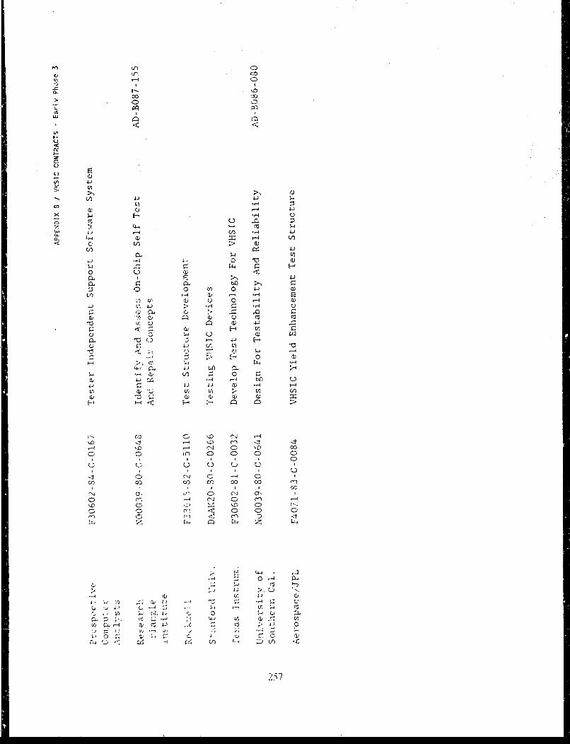
cl; ri
>c CX
Li
u
cu c
I4J)
C. U
m C.) *-4
(4-.- b- o 5
4a J'l ) -4 U
V) V,) V) U
UC) 00 4
-CD 2- '4 CD Hor cr) co -C ID 0
U) r- 0) I "I 2
0WQ C r-A C
'0~~ -4 0 0 4
C-Q '0(3 -4- 4
-4 tr 42) -1')'0 q Q, cc
1) - Cs U) -Cs 4 Z .. I .4 bO
4.1~~~ý C i 4 ) - n -
CI)~~~~ 7I ) .. C) U
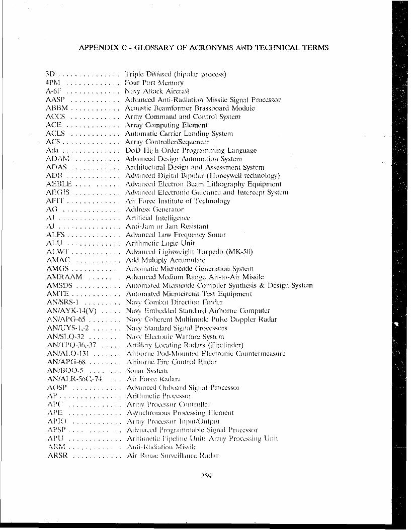
APPENDIX C - GYLOSSARY OF'ACRONYMS AN4D IECI NICAL TERMS
3D ý . . . . . . . .T1riple Diffused (bipolar process)4PM.l..............Four Po)rt MemiorvA-61 ............... Nawy A!Zack AircraftAASP..............Advanced Anti-Radiation Missile Signal1 Proce'ssorABBM ............. Acoustic Beamtformer Brassboard 'vodIuIeACCS..............Army Command and Control SystemnACE .. .. .. .. .. .. .... Array CompuLting ElementACLS..............Automatic Carrier Landing SystemnAC-S...............Array Controller/SequencerAda................ DoD H1i, h Order Programming Language,'ADAM.............Advanced D~esign Automation SystemADAS.............. Architectural Design and Assessment SystemADI . .............. Advanced Digital Bipolar (1 loneywell technology)AEI3LE...........Adlvanlced Electron Beam Litbography EquipmentA\EGIS.............Advancedl Electronic (3uidanc.o and Intercept SystemAFYI ............... Air Force Institute of Te~chnologyAG................Address GieneratorAT................. Artificial I nteliienccAl ................ Anti -. am or Jam ResistantALFS .............. Advanced Low Freqluency SonarALU...............Arithmectic Logic UnitAl WIJ..............Adva nced 1.igh tweight Torpedo (MiVK-50)NAMC..........Add Multiply Accumulate
AMMS.......Automatic Microcode Generation SystemAM RAAM..........Advanced Medium Range Air-to-Air MissileAMISDS ............. AutomAted Microcode Compiler Synthesis & Design SystemnAMITE............ .. 'Xutomated Microcircuit '1l--st EquiprncniAN/SRS-1...........Navy Conflbat Direction FinderAN/AYK- 14(V).......Navy, Em'nbedded Standaird Airborne Compu1-AterAN/APG-65 ........ ..Nay Cohecrent Multimode P~ulse Doppler RadarAN/UJYS- 1 --2......... Navy Standard Signal I'rocesmorsAN/SI .0-32..........Nav leioi Warffae;M SVStLm1ANf11'0-36,-37.......Artillery L( lati n, Radars (Flireindcr)AN/A\l-0-131.........Airborne 1Pod-N~omnted Electonic CounterimeasureANIATPGi-68 ......... Airborne Fire Control Radari\N/1300-5...........onar Sy~stemAN/Al-R-50C(-.74 . .. Air Force Radar;;A( SP..............Adva neecd 01)nb )ard Sil~hid Pro-(cessoIA~ll.................\Arihi iltic P~rocessorAP( ................ Arr.ay l'ri )C55O ControllerAPE1. .............. Asvncl ronons 11rocessi n F~ ElmentA'ITI)..............Ar ray P'rocessor 1 npimt/( at putAIPSP........... ... Adwnaced Inreyamable Shi':ial 1'roccssmrAIPtUi..............Ait hinletic P i pchei U nit; Arm:.' 1'rocss;in Unit
ARSIZ..............Air Roic Surtveillance Radar
2.59

AP'PEND)IX C'/ GLOSSARY
A S C IV ....... daced Spaceborne Cornputer ModuleASK ........ Application Spec~ific 11nreg,"aretd Circu.itASP ....... Advanced Signoal Processor
;%,w . ... ... ... Anntsublmarinli Wa rfareATA ....... AdvanIcedI~acticai AircraftA 1- 1 ...... Automatic: 1est EquipmentAT1F .... ... A~dvatm.1 TVactical Figi'hterATI- ....... Advanced Technolcgy I 1clicopter
ATI M.............. Advanced '1'cchnoltzy Insertion ModuleATPG.............Automatic Tecst Pattern GenerationATIR...............Automatic (or Aided) T1'arget RecognitionAU............... .Arithmetic UnitAV-SB3.. .. .. .. . . . .. arinc Vertical Takeoff and Landint, (VTOL) AircraftAWA-S ............ Airborne Warning anIotolSeAWlS..............Advanced Wafer Imaging SvstemBEOL .............. Back End of LineJBiC.MOS............Bipolar ind CMOS combined on a chipBILB3()............Built-jo Logic Block, Observer13 1ST....... ........ Built-in Self T'estB F1'................Built-Tn VestBill ............... Biis Interface UnitBOPS..............Billionl Operations Per Second(BPS('J.............Borophosphosilicate GlassBrass~board .......... 7iel]d Demniost rable Electronic ModelBreadboard.......... Labortory Demonstrable Ele-ctroniic ModelBSO...............Bias Sputtered QuairtzBSlS ............... Boost Surveillance and TIracking SystemC31................Command, Control, Communications, and IntelligenceC4 ................. Coitrolled Collapsible Clhip Connection (IB1M)CAD ............... Computer Aided DesignCALMA............Graphics design system mairketed by CALMA CorporationCAL-S..............C'omputer Aided Acquidsition and Logistics SystemCAM .............. Computer-Assisted ManuifacturingCAM .............. Content Addresslable Memory'CAP-32............. 32-Bit Common Avionics ProcessorCAVP..............Compniilex Arithmetic Vector ProcessorCC-BUS............Chip to Chip BusCCS/MK 2 .......... Command Control Software foi 135\'- SI SbmarineCDP...............Configurable Data Path (chiip)CDR ............... Critical De~sign ReviewCDRL. ............. Contract Data Req uirements List(TI................ CAD Framework InitiativeCGA ............... Con Iivinrable G a te ArrayCMAC ............. Complex Multiply AccuuniduateCMAG.............Cruise Missile Advanced (itlidancCC;M L...............(2urren t mode LogicC;M O's.............ComIIp~lementary Metlal-( xide Semiconductor
200
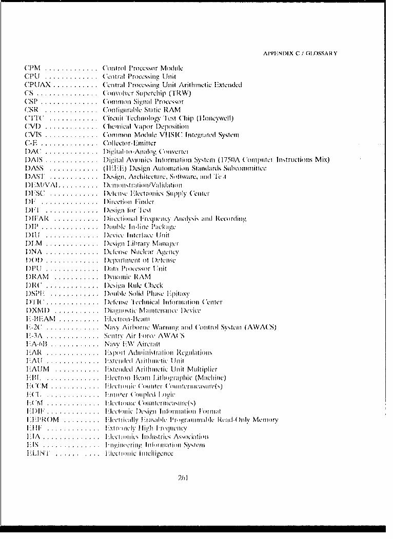
API'IINIIX C / CLOSSAH Y
CJ'NI . . . . . .. C~ontrol P~rocessor M~oduileCPU ......... Central I'roccssiniz UiotCPUA.JX ...... (Cntral P'rocessingi. tnil Arithimetic IFxtcndcd
CS ............... Conmvulvcr Supiprchip (TRW)
CS R ....... (Titigirai~c Static RANIYIT( ........ Circuiti I ch I1()lgy Tu-st C hip (H oncvwell)
cV) ....... I Chemi cal V'apor lDcposit ion(NIS ........ Cmonrni Modulle V! ISI( Ilitogratd Systemi
C- .. ..... ... II (I I COI mI o r- I 'mi t cr
DAi\IS ....... Digi~tal Avionics Intormation System (1 750A C onlptltc Jn..triictic ns M~ix)IJASS ............ (IFFFI ) I )sigin Autionuit ion StanI~dards Sithconimit teeI)ASI ............ Ilesil.,i, Architecture, Software, im l~e
1)1 C . .. .. .. . IM)L-cn1,c FI -Clcct iCS Supply ( I N k1: ... .. ... .. I)irection i n,1ILr
1)11 . . . . . .. Di.sivii l)r 'lestl1) 1 FA:, . .. .. .. D RCI(i M.ti~u'i1 lIL(I(IL ,\n;,Ivsis and IRcc'rdinuw.D)1I' . . . . . .. I Double In--hue 1'ackai.c1)IU~ ... . .. . . DL IC n rla~IlILce Uf itI)I.M ............. Ikcsign I .ihrary NImana .rcD NA ....... IDetcrise NuIcIlear Ap.nyD ( )l .. . .. . . . DýJII)cp rttCII 0tI )Lk'itc Se
I IAN~I ... . . . yI )nmic RAN'IDR( ....... IDcs~il~ R1ule Check,I)SPI:ý .,...... ... D~oubhle Solid l'lltw~ LpIitaIXNDIC )'l .IelCnise lc'chnicauI IinlOrt11tio)l C enter
F-I; AX Nl) .,......... 1: 1i 11t U;,i Vancntc ~v
I-(................Navy Ai ihoruc Vari i nv andu ( n0t1' SystemLIl (A\WAC S)E -3A ............... tI SC\. Alir FOR AWAC SI,-6 A(I.............. Navwy I .W AircraftI AR(................Ixport Aduuintstiat:(un Rugiulatucums
I iA UJN.. ........... IAte R jdir it ultic I.nit Nl t p e
fI( '1.................Ixtenduin' r itici (ni MidpILI I.oeFif.( [..............IIcui(Iltrleanc)lI " CC..............Ilc'ii u~siu It r uItIoIv;Iu I rn (StI - I .ll~ .. '...........I Itetri-al Ljat ahIc I~o'r'jriniI vil( c% M m r
1.1 II...............I-AtIM ituCl I ughlIttijtcs uscy~i
1F.Is.............I'li lucincerfiug ItM Illatio~n Svstcil...... oui i....e~n
261
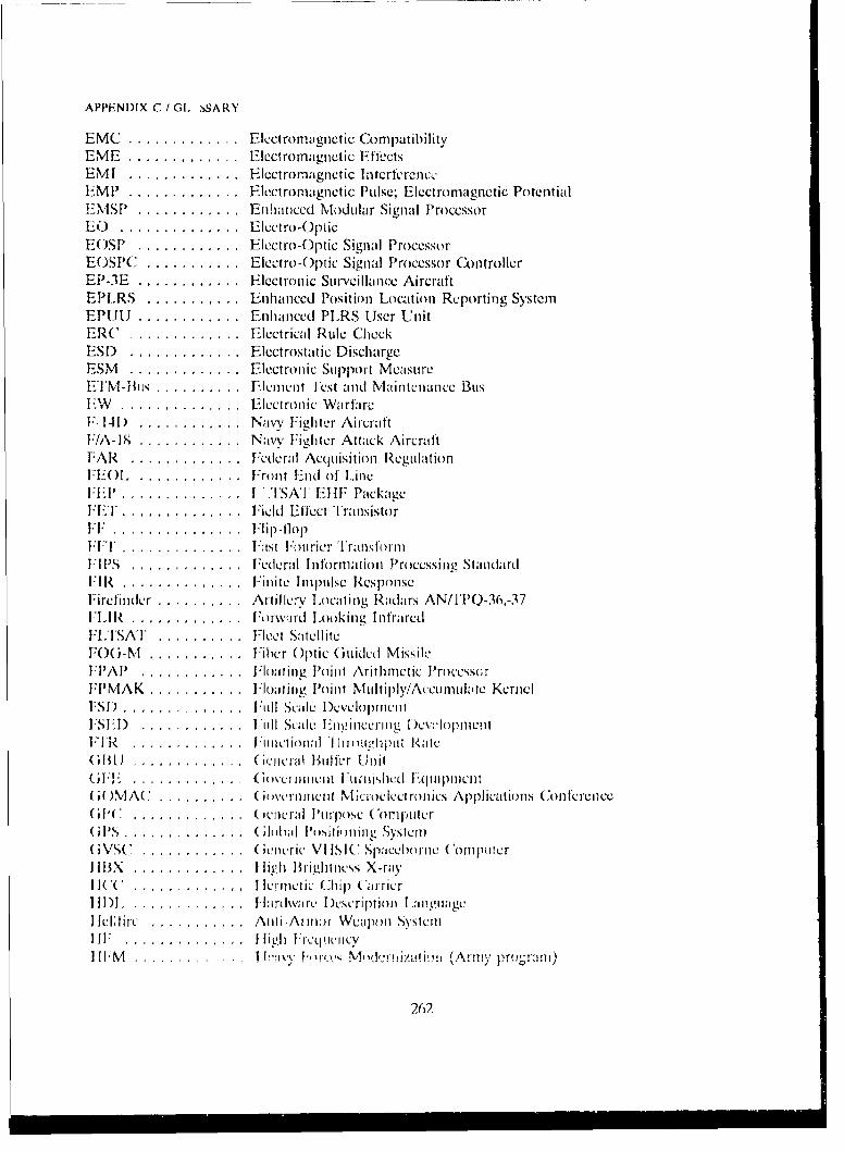
APPENDIX C / G1- sSARY
EMC ............. Elctrom iagnetic CompatibilityEME ............. Ilectromaguctic EffectsEM .I ............. Electromagnctic InterfereneeEM1 .............. Electromagnetic Pulse; Electromagnetic PotentialEMSP ............ Enhanced Modular Signal Processor
EO .............. Electro-Opt icEOSP ............ Electro-Optic Signal ProcessorEOSPC ........... Electro-Optic Signal Processor ControllerEP-3E ............ Electronic Surveillance AircraftEPLRS ........... Enhanced Positimn Location Reporting SystemEPJU ............ Enhanced PLRS User UnitERC( . ............. Electrical Rule CheckES ). ............. Electrostatic DischargeESM ............. Electronic Support MeasureEI'M-Bu ........... E-lemnt lest and Maintenance Bus
W ................. Electronic WarfareF-14!) ............ Navy Fight,.r Aircraft-IA- 18 ............ Navy Fighlter Attack Aircraft
F AR ............. Federal Acquisition RegulationFT-0L.. ............ Front End of LineIT11............... I '.TSA EJIF PackageELT. ........... .Fied Effect Tlransistor:1F ............... . .Flip-llop
FFI. ................ "ast Fouirier TransformFIPS ............. Fcdcral Informat ion Processing StandardFIR ........... ... I Finite 1I111lsC Response
Firefindcr .......... Artillery Locatiing Radars AN/1PQ-36,-37FIIR ............. I r)rw rd Looking InfraredIT ISA'' . .......... Fleet SitcllitcFO( i-M ........... . lihcr Optic (iuidcd MissilcFI'AP ............ ... hating Point Arithmetic I'roccss(;rI: MAIK ........... Floating Poi nt Multiply/Accu uim ,itc Kernel
FISD ........ ... ,. F:ull Scleu I)evclpimeniFS 1II) ............ Fuill Scale Luncinccring DCvclopntenlIIR ............. . Functional 'I him tiliput Rate(61111 .......... I.. G( cn ral Bulfer Unit
G Il. ............. (hoeiuntc'nt FiruislihCd E;.q lIpieCnt(iW)MA( ............. (icvrnnient Ni,-iclectlronlics Applications Confcrelnce; H'(. ................ (iunr;il Purp.oec (omprlutcr
( ilS .............. ( lohhal I'NSilimling SvSteni( iVs(. ............ (C, ric VI IS I Spacehorne o Conpiuler
II fiX ............ II ligh llrightlness X-ray
I1( . ............. I lerm ctic Chip C-1arricr
III) ............... ].Lirdwa rc I)escription I an unagclllllire, Anti-Airmmii; Weapon SystemnI 1. ............... Ii gh l:r(cq itlincyI1I1 ...... ........ 1 h,•iv , , .M,,e,.'i/',ti~t (A ,i.y pr.m rann)
262
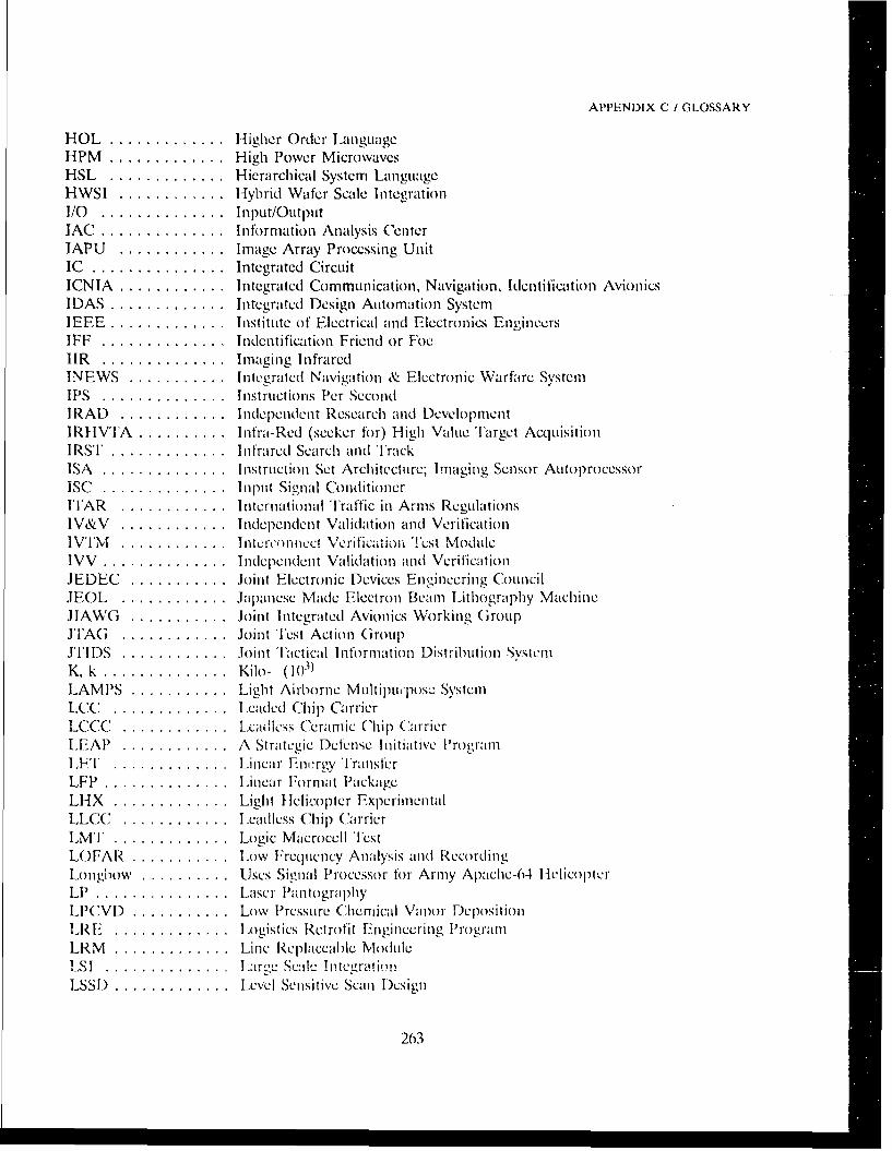
APPFiNIIX C /GLOSSARY
HOL ....... Higher Order LanguageHPM ....... High Power MicrowavesHSL ....... Hierarchicil Systcem LanguageHWSL ........ ybrid Wafer Scale Integration1/0 . . .. . . . InI)Ult/()UtptltIAC ............... Information Analysis CenterIAPU..............Image Array Processing UnitIC ................. Integrated CircuitICN IA ............. Integrated Communication, Navigation, Identification AvionicsIDAS .............. Tntegratcd Design Automation SystemIEEE .............. Institute of Electrical and Electronic,; Engineers1FF ................ 1Indentification Friend or FoeUR................Imaging InfraredIN EWS............. Integrated Navigation & Electronic Warfarc SystemIPS................Instructions Per SecondIRAD..............Independenlt Research and DevelopmentI R 1VlA ........... Infra-Red (seeker for) High Value Tlarget AcquisitionI RS'T.............. Infrared Search and TIrackISA ................ Instruction Set ArchlitecCture; Imaging Sensor Au.toprocessorISC................Input Signal ConditionerlIAR..............International TIraffic in Arms RegulationsIV&V..............Independent Validation and VerificationIVT'IM..............Interconneict verificl.tioni Test ModuleIVV .............. I nIMependenC~t Validation and VerificationJEDEC.............Joint Electronic Devices Envineering CouncilJE(.L..............Japanese Made Electron Beami Lithography MachineJ IAWG.............Joint Integrated Avionics Working GiroupJ'1AG..............Joint lest Act ion Oiroup.JII DS)5............. Joint Tlactical Information Distribution SystemlK. k ............... Kilo- (,i) 3 )
LAMPS ............ Light Airborne Mutlt ipu tpos, SystemLCC .. ............. Leaded Chip C~arrierLCCC..............L~cadless Ceramic Chip C.arrierLEAP..............A Strategic Defense Initiative 1ProgramiLEEl. .............. Linear Eniwrgv TIransferLFP...............Linear Formiat PackageLHX............... Light helilcopter ExperimentalLLCC .............. Leadless Chip CarrierLM'I ............... Logic Macrocell 'VestLOFAR ............ Low Frequency Analysis and RecordingLongbow............ Uses Signal Processor for Armiy Apachec-64 lielicopte:rL1 ................ Laser PantlographyLPCVD ............ Low Pressure C'hemical Vaioor DepositionLRU .. ............. I Logistics Retrofit Enginec ring P'rogramLRM ............... Line Replaceable Moduleis!................1.~g Scdle integrationLssDl)..............Level Senisitive Scan Design
263
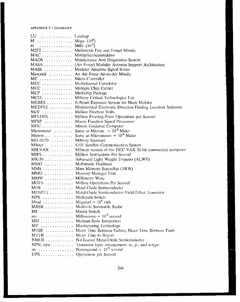
APPENDIX C / GLOSSARY
LU................ LatchupM................. Mega-, (1( 6)
I....................Milli- Ow0-)M2F2............... Multim''odc Fire and Forg~et M~issileMAC ............... Multiplieir/AccumnulatorMADS .............. Mairtcrnane And Diagnostics SystemMASA .............. (Air F~orce) Modular Avionics Support ArchitectureMASS...............Modular Adaptive Signal SorterMaverick.............An Air Force Air-to-Air MissileMC................ Micro.-ControllcrMCC............ Multichannel CorrclatorMCC...............N'ltltiple Chip CarrierMCP................Multicliip PackageMC LL..............Military Critical Iechnologies ListMEBES ............. E-Beamn Exp)osure SySteml for Mask MakingMEDFLI ............ Miniatuirized Electronic Direction Finding Location IndicaitorMeV................Million Electron VoltsMFLOPS ............ Million Floating-Point Operations- l)c SecondMFSP.............. Macro Function Signal ProcesssorMGC ............... Missile, Guidance ComputerMicrometer...........Same as Micron: =10.6 MeterMicron.............. Same as Micromeiter: = (1-6 MeterM I L-SID............ Military StandardMilstar .............. ElIF Satellite Commnunication SystemMILVAX............ Military version ot the DEC' VAX 32-bit commeircial computerMIPS ............... Million Instructions Per SecondMK-50 .............. Advanced Light Weig~ht Torpedo (ALW'l')MMG.............. Multirnode GuidtcanceMMS ............... Mass Mcnioty Superchip (TRW)MMU.............. Memory' Manager UnitNMMX.............. Millimeter WaveMOPS.............. Million Operations Per SecondMOS........... .... Metail-Oxidc ScmiconductcrMNOSFEA ............ Metal-OXIdeC Semiconductor Field Etfect TranisistorNIPS............... MUltipathl Sw'itchMrad............... Megarad - 10 6 radsMIRSR .............. Mul1tirle01 Survivable RadarMIS................ Matrix SwitchIls ...... ............ Millisecondu 1- SecondLMSJ................ Medium Scale IntegrationMl' ................. Mauifactutring T1echnologM']13F...............Mean I'lime Between Failure; Mean 'lime Betwceen FaultM'UI*R.............. Mean Time to RepairNMOS .............. N-(liannel Metal-Oxide SemiconductorNPN, npn............ .Transistor layer arrangemecnt: n-, p-, anld n-typeris.................. Nanosecond= 10(-9 second
OPS................ Operations per Second
264

APPENDIX C I GLOSSARY
OSD ............. Office of the Secretary of DefenseOUSDA ........... Office of the Under Secretary of Defense for AcquisitionOUSDRE ......... Office of the Under Secretary of Defense for Research and EngineeringP3-C..............Nawv ASW AircraftP3 ............... Naval Patrol AircraftP31 .............. Preplanned Product ImprovcrcmntPatriott ............. An Army Ground BMsed RadarPAU ............. Pipeline Arithmetic UnitPave Sprinter ....... .Modular Avionics Demonstration ProgramPE ............... Processing ElementPECVD ............ Plasma Enhianced Chemnical Vapor Deposi~ionPG A .............. Pin Grid ArrayPI-BUS ........... Parallel Interface Bus (designed during VHSIC-2)PISCES ........... A Device Modcling/Simulation CodePJH .............. PLRS/J'IDS HybridPLA ............. Programmable Logic ArrayPLAU ............ Pipeline Arithmetic UnitPLRS ............. Position Location Reporting SystemPN .............. . Pscudo NoisePNP, pnp .......... .. ransistor layer arrangement: p-, n-, and p-typePOC. ............. Proof of ConceptPolysilicide ......... Polvcrystallinc Silicon-Metal CompoLund (C. g. MoSi2 )PPPj .............. Parallcl Pipeline Proces,;orPRDA ............ Project Rescarch & Development AnnouncementPrism ............. A classified military programPR()M ............ Programmable Read-Only MemoryPSG .............. Phlosphosilicate GlassPSP .............. Programmable Signal ProcessorPWB ............. Printed Wiring BoardOCI .............. Qualification Conformance InspectionQML ............. . Qualified Manutfacturers ListOPL ............. Oualified Products ListRALU ............ Register Arithmetic Logic UnitRAM ............. Random Access MenmoryRFI .............. Radio Fre(quency InterferenceRF . ............. . Request for ProposalsRIIVP ....... ..... Radiation 1lard Vector ProcesorRI-1-32 ............ Radialtion Hard 32-bit ProcessorRIE .............. Rcaclive Ion EtchRISC .............. Redluced Instruction Set ComputerRISCAE .......... Ruduccd Instruction Set Comp)uter Ada EnvironmelntROM ............. Read Only MemoryRoX ............. ReccssCd OxidcRPV ............. Rcmotcly Piloted VehicleRT ............... Register Transfer LanguageRW R ............. Ri't:ir W irnin i. ReceiverS3 ............... Naval Early Warning Aircraft (including, rada11r system)
265
APPENDIX C I GLOSSARY
SABIR ............ Space Based Intcrceptor programSAFE ............ Self Aligncd Field EdgcSCC .............. Singlc Channel CorrclatorSCM ............. Single-Chip Module (used interchangeably with SCP)SCP .............. Single-Chip Package (used interchangeably with SCM)SDI .............. Strategic Defense InitiativeSDS .............. Strategic Defcnsc SystemSEC .............. Standard Evaluation CircuitSECDED .......... Single Error Correct, Double Error DetectSEM ............. Standard Electronic ModuleSEMATECH ....... An Industrial Semiconductor Development ConsortiumSEP .............. Standard Extremely High Frcquency (EHF) PackageSEU ............. Speech Enhanccment UnitSEU ............. Single-Event UpsetSGEMP ........... System Generated Electromagnetic PulseSH-60B ........... (Sikorsky) Helicopter AircraftSI Chip ........... System Interface Chip (BIU + FlU)SiCB ............. Silicon Circuit BoardSkGINT ............ Signal IntelligenceSINCGARS ........ Singlc Channel Ground and Airborne Radio SystemSLAM ............ Scanning Laser Acoustic MicroscopeSOI .............. Silicon on InsulatorSOS .............. Silicon on SapphireSOW ............. Statement of WorkSP ............... Signal ProcessorSPARC ........... Scalable Processor ArchitectureSPE .............. Signal Processing ElementSPEAR ........... .Solid Phase Epitaxy and RegrowthSPICE ............ Public Domain Integrated Circuit Simulation ProgramSPS .............. Systolic Processing Superchip (TRW)SOC/SPC .......... Statistical Quality & Process C:ntrolSRAM ............ Static Random Access MemorySRAM ............ Short Range Attack MissileSSI .............. Small Scale IntegrationSTACK ........... Standard Computer KompentenSTCP ............. Self "lcst Configuration ProcessorSTL .............. Schottky Transistor LogicSTS .............. Signal Tracking SubsystemSubACS ........... Submarine Advanced Combat SystemSWAP ............ Size, Weight, and PowerSYSCLK .......... System ClockTAB ............. .. ape Automated BondingTAM ............. l'hreat Association ModuleTD .............. 'otal DoseTDL ............. .. est Description LanguageTEA ............. .. est Engincer's AssistantTISSS ............ .ester Independent Support Software System
2,6
AIPPENIIX C IGLOSSARY
TI U............. . Fest interFace Unit (Honeywell)FM-BS......... 'ietnd Maintcniance Bus
TOW ............. . 'lube Launched, Optically '[racked, Wire Guided MissileTlREE ............ . ransicnt Radiation Effects in ElectronicsTISL .............. .''cst Specification LanguageTF IL.............. .I ransistor-TIransistor Logic.TVL..............'I',ISSS Vector LanguageVAG .............. Vector Address GeneratorVAL .............. VHDL Annotation LanguageVALU ............. Vector Arithmetic/Logic UnitVAMP ............. VHISIC Avionics Modular ProcessorVAX .............. DEC 32-Bit Commercial ComputerVBIU............. VHSIC Bus Interface UnitVCB.............. VHSTC Communications BrassboardVCC .............. VFISIC Central Computer (for F-15)VCP.............. VIISIC Communlications ProcessorVDEG ............. VHDL Design Exchange GroupJ-VHDL ............. VHSIC H-ardwvare Description LanguageVHSIC............ Very High Speed Integrated CircuitsVID ............... VHSIC Insertion Demonstration for the EMSI'VIFASG........... VHDL Intermediate Form. Analysis, and Slaudardization GroupVLM .............. Very L'irge MemoryVL-SI .............. Very Large Scale IntegrationVNMASS ............ VliSIC Modular Adaptive Signal SorterVMDV............ VHDL Model Development and ValidationVMIE Bus............Standard Digital Equipment Corporation B~usVPC .............. Vector Pr-oduct CalculatorVPM .............. VHISI(: Processor ModuleVP(.)..............(DoD) VI-ISIC Program OfficeVPSP .............. VI-SIC Programmable Soinal ProcessorVS( ............... VHISIC Siuna'il ConditionerVTAM ............. VI lSl(: 'lireat Association ModuleVIB.............. VIS IC 'lerminal lBrassboardV'VCA ............. VI-ISIC 'lransrnit Coot rol AssemblyWAM............. Window Addressable MemoryWAVES............Waveform and Vector ExchanLW SpecificationWCI ............... Wireless Command LinkWNC .............. Weapons Navigation ComputerWSI ............... Wafer Scale IntegrationXSAR ............. X-ray' Step) and Repea't Lithlographiic Mach tineYAG ............... Yttrium Aluminum GarnetYE............... Yield EnhancementYVR .............. Yield Verification Run
267
Related Documents