W&M ScholarWorks W&M ScholarWorks Dissertations, Theses, and Masters Projects Theses, Dissertations, & Master Projects 2017 Vertically Oriented Graphene Electric Double Layer Capacitors Vertically Oriented Graphene Electric Double Layer Capacitors Dilshan V. Premathilake College of William and Mary, [email protected] Follow this and additional works at: https://scholarworks.wm.edu/etd Part of the Nanoscience and Nanotechnology Commons Recommended Citation Recommended Citation Premathilake, Dilshan V., "Vertically Oriented Graphene Electric Double Layer Capacitors" (2017). Dissertations, Theses, and Masters Projects. Paper 1516639673. http://dx.doi.org/doi:10.21220/S2RH36 This Dissertation is brought to you for free and open access by the Theses, Dissertations, & Master Projects at W&M ScholarWorks. It has been accepted for inclusion in Dissertations, Theses, and Masters Projects by an authorized administrator of W&M ScholarWorks. For more information, please contact [email protected].

Welcome message from author
This document is posted to help you gain knowledge. Please leave a comment to let me know what you think about it! Share it to your friends and learn new things together.
Transcript
W&M ScholarWorks W&M ScholarWorks
Dissertations, Theses, and Masters Projects Theses, Dissertations, & Master Projects
2017
Vertically Oriented Graphene Electric Double Layer Capacitors Vertically Oriented Graphene Electric Double Layer Capacitors
Dilshan V. Premathilake College of William and Mary, [email protected]
Follow this and additional works at: https://scholarworks.wm.edu/etd
Part of the Nanoscience and Nanotechnology Commons
Recommended Citation Recommended Citation Premathilake, Dilshan V., "Vertically Oriented Graphene Electric Double Layer Capacitors" (2017). Dissertations, Theses, and Masters Projects. Paper 1516639673. http://dx.doi.org/doi:10.21220/S2RH36
This Dissertation is brought to you for free and open access by the Theses, Dissertations, & Master Projects at W&M ScholarWorks. It has been accepted for inclusion in Dissertations, Theses, and Masters Projects by an authorized administrator of W&M ScholarWorks. For more information, please contact [email protected].
Vertically Oriented Graphene Electric Double Layer Capacitors
Dilshan Viraj Premathilake
Kandy, Sri Lanka
Master of Science, Old Dominion University ,2011 Bachelor of Science, University of Peradeniya, 2008
A Dissertation presented to the Graduate Faculty of The College of William & Mary in Candidacy for the Degree of
Doctor of Philosophy
Department of Applied Science
College of William & Mary June 2017
ABSTRACT
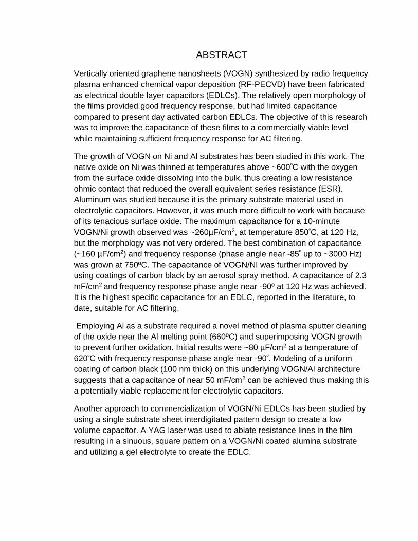
Vertically oriented graphene nanosheets (VOGN) synthesized by radio frequency
plasma enhanced chemical vapor deposition (RF-PECVD) have been fabricated
as electrical double layer capacitors (EDLCs). The relatively open morphology of
the films provided good frequency response, but had limited capacitance
compared to present day activated carbon EDLCs. The objective of this research
was to improve the capacitance of these films to a commercially viable level
while maintaining sufficient frequency response for AC filtering.
The growth of VOGN on Ni and Al substrates has been studied in this work. The
native oxide on Ni was thinned at temperatures above ~600ºC with the oxygen
from the surface oxide dissolving into the bulk, thus creating a low resistance
ohmic contact that reduced the overall equivalent series resistance (ESR).
Aluminum was studied because it is the primary substrate material used in
electrolytic capacitors. However, it was much more difficult to work with because
of its tenacious surface oxide. The maximum capacitance for a 10-minute
VOGN/Ni growth observed was ~260µF/cm2, at temperature 850ºC, at 120 Hz,
but the morphology was not very ordered. The best combination of capacitance
(~160 µF/cm2) and frequency response (phase angle near -85º up to ~3000 Hz)
was grown at 750ºC. The capacitance of VOGN/NI was further improved by
using coatings of carbon black by an aerosol spray method. A capacitance of 2.3
mF/cm2 and frequency response phase angle near -90º at 120 Hz was achieved.
It is the highest specific capacitance for an EDLC, reported in the literature, to
date, suitable for AC filtering.
Employing Al as a substrate required a novel method of plasma sputter cleaning
of the oxide near the Al melting point (660ºC) and superimposing VOGN growth
to prevent further oxidation. Initial results were ~80 µF/cm2 at a temperature of
620ºC with frequency response phase angle near -90º. Modeling of a uniform
coating of carbon black (100 nm thick) on this underlying VOGN/Al architecture
suggests that a capacitance of near 50 mF/cm2 can be achieved thus making this
a potentially viable replacement for electrolytic capacitors.
Another approach to commercialization of VOGN/Ni EDLCs has been studied by
using a single substrate sheet interdigitated pattern design to create a low
volume capacitor. A YAG laser was used to ablate resistance lines in the film
resulting in a sinuous, square pattern on a VOGN/Ni coated alumina substrate
and utilizing a gel electrolyte to create the EDLC.
i
TABLE OF CONTENTS
Acknowledgement iii
List of Figures iv
Chapter 1. Introduction 1
1.1. Electric double layer capacitors (EDLCs) history and
e development 1
1.2 EDLCs from vertically oriented graphene sheets 4
1.3 Objectives and organization of dissertation 5
Chapter 2. Theoretical background 6
2.1 Graphene 6
2.2 Introduction to EDLC 7
2.3 Electrochemical impedance spectroscopy (EIS) 16
Chapter 3. Characterization diagnostics and growth chamber 22
3.1 Scanning electron microscope (SEM) 22
3.2 Raman spectroscopy 24
3.3 Auger electron spectroscopy 28
3.4 Electrochemical impedance spectroscopy (EIS) 31
3.5 Radio frequency plasma enhanced chemical vapor deposition
s system (RF- PECVD) 32
3.5.1 The matching network 35
Chapter 4. VOGN on Ni 37
4.1 Pre-growth characterization 37
4.2 Acetylene plasma and formation of VOGN 39
4.3 EDLC cell formation 41
4.4 Characterization and performance of VOGN on Ni 45
4.5 Raman spectroscopy of VOGN 50
Chapter 5. VOGN on Al 52
5.1 Introduction 52
5.2 Experimental 52
5.3 Results 55
5.4 Discussion 67
ii
Chapter 6. Carbon black coating on VOGN 70
6.1 Introduction. 70
6.2 Experimental. 71
6.2.1 RF PECVD system. 71
6.2.2 Diagnostic systems. 72
6.2.3 Coating method. 73
6.2.4 VOGN architecture. 74
6.2.5 Carbon black coating 76
6.2.6 EDLCs. 76
6.3 Results 77
6.3.1 Topography 77
6.3.2 Raman spectroscopy 80
6.3.3 Electrochemical impedance spectroscopy 81
6.4 Discussion. 85
6.4.1 RF-PECVD plasma. 85
6.4.2 Ni substrates. 86
6.4.3 Carbon coating. 86
6.4.4 Raman data. 87
6.4.5 Electrochemical impedance measurements. 87
6.4.6 COMSOL modeling of a uniform 100 nm CB coating on
V VOGN/Ni. 88
6.5 Summary. 90
Chapter 7. Planar interdigitated EDLC design 91
Chapter 8. Summary and future work 99
References 104
Vita 109

iii
Acknowledgement
I would like to sincerely thank my adviser, Professor R.A. Outlaw for his patient
guidance and mentoring throughout this doctoral program. I will always be in debt
for his support and advice in all aspects of my life.
I would also like to thank the collaborators, Dr. John Miller who has helped us to
secure funding for this project and with experimental work at his company, JME
Capacitors and Dr Sam Parler of Cornell Dubilier for helping us with valuable
advice on capacitor modeling and commercialization of capacitors.
I would also like to thank the Army Research Lab for providing the funding for this
dissertation work under the SBIR topic no. A11-013 “Graphene based electric
double layer capacitor”.
I am extremely grateful to the staff at the Applied Research Center, especially to
Richard Proper, Amy Wilkerson and Olga Trofimova for their help with operating
the diagnostic equipment and laboratory support.
I am also grateful to the College of William and Mary Applied Science Department
for choosing me for graduate work and especially the department head, Dr.
Christopher Del Negro.
Last, I would like to thank my parents for their immense help and support in my life
that has led me to this point.
iv
List of Figures
Figure 1.1: Comparison of size between Supercapacitor of 350F (left) with electrolytic
capacitor of 0.047 F(right)............................................................................................... 2
Figure 1.2: Phase angles for 350 F commercial EDLC and 0.047 aluminum electrolytic
capacitor. ........................................................................................................................ 3
Figure 2.1: Hexagonal structure of graphene, including the orbital hybridization ............. 6
Figure 2.2: Diagram of a symmetric EDLC capacitor cell ................................................ 8
Figure 2.3: Helmholtz model of the double layer. ...........................................................10
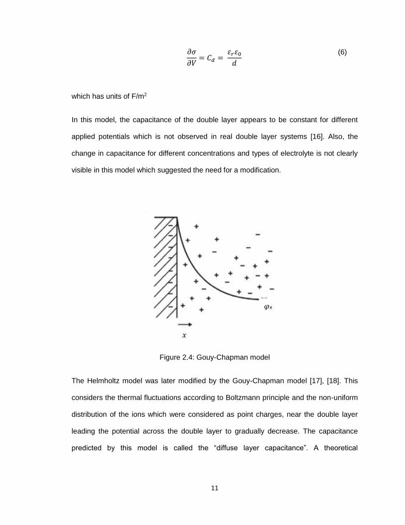
Figure 2.4: Gouy-Chapman model .................................................................................11
Figure 2.5: Stern model .................................................................................................15
Figure 2.6: Bockris-Devanathan-Muller model ...............................................................16
Figure 2.7: R-C circuit diagram ......................................................................................19
Figure 2.8: (a) Nyquist diagram of R-C circuit with ESR and Faradaic type behavior (b)
without Faradaic behavior. .............................................................................................20
Figure 2.9: Basic Nyquist plot for porous electrode behavior .........................................20
Figure 2.9: A typical representation of a Nyquist plot .....................................................21
Figure 3.1: S-4700 scanning electron microscope ........................................................22
Figure 3.2: Schematic of internal mechanism of a typical scanning electron microscope
......................................................................................................................................24
Figure 3.3: The orange and blue lines represent the Raman process. The red represents
Rayleigh scattering ........................................................................................................26
Figure 3.4: Raman spectra of pristine (top) and disordered (bottom)graphene.[29] .......26
Figure 3.5: Renishaw inVia Raman spectroscope .........................................................27
Figure 3.6: Schematic of the Auger process ..................................................................28
Figure 3.7: (a) The apparatus used for AES testing (b) Auger Spectrum taken for VOGN
on Ni and pure Ni ..........................................................................................................30
Figure 3.8: (a): Coin cell testing procedure for VOGN on Ni coin cells. Tab 1 and 2 are
connected to the above-mentioned equipment terminals. (b) Frequency Response
Analyzer (FRA), Solartron model 1255 ..........................................................................32
Figure 3.9: Schematic of the RF-PECVD system ...........................................................33
Figure 3.10: (a) The RF power supply and control unit (b) The RF-PECVD matching
network. (c) RF antenna top hat enclosure. (d) RF-PECVD vacuum growth chamber. ..33
Figure 3.11: (a) The interior of the top hat. The RF power is channeled to the chamber
through this coiled copper antenna with refrigerant cooling. (b) Close-up of the alumina
heater while heated. The Ta mask can be seen here on top of two VOGN coated Ni foils.
......................................................................................................................................34
Figure 3.12: Equivalent circuit of RF-PECVD system ....................................................35
Figure 3.13: Picture of matching network used in the RF-PECVD growth chamber .......36
Figure 4.1: Normalized oxygen Auger peak to peak height vs temperature [32]. The
decrease in the ratio at ~300ºC is the loss of surface O by reaction with surface C and
the subsequent dissolution of the O into the Ni bulk. .....................................................38
v
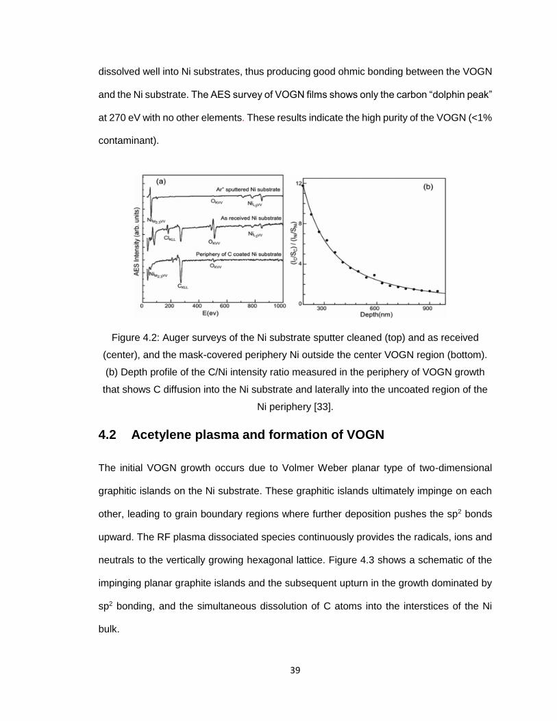
Figure 4.2: Auger surveys of the Ni substrate sputter cleaned (top) and as received
(center), and the mask-covered periphery Ni outside the center VOGN region (bottom).
(b) Depth profile of the C/Ni intensity ratio measured in the periphery of VOGN growth
that shows C diffusion into the Ni substrate and laterally into the uncoated region of the
Ni periphery [33]. ...........................................................................................................39
Figure 4.3: Schematic of VOGN growth due to graphite island impingement .................40
Figure 4.4: (top) VOGN grown Ni electrode pair. (bottom) the heavy Ta mask used to
define the growth region and insure uniform heat distribution of Ni substrates. ..............42
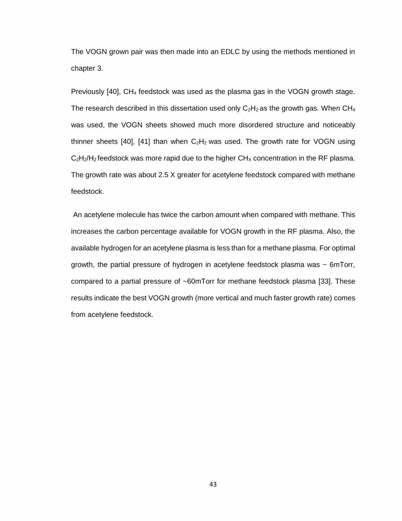
Figure 4.5: Temperature calibration graph for the Al2O3 heater......................................44
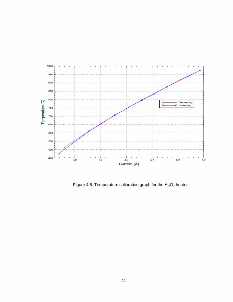
Figure 4.6: Morphology of VOGN on Ni for different substrate temperature. Scale bar is 1
µm .................................................................................................................................45
Figure 4.7: (a) Phase angle vs frequency graph (b) Complex plane plot for temperatures
from 620ºC-850ºC. The inset shows a vertical intersection with the X axis which shows
no porous electrode behavior and ESR levels between 0.07-0.08 Ω .............................46
Figure 4.8: (a) Specific capacitance as a function of temperature (note specific
capacitance at 120 Hz) (b) Specific capacitance as a function of temperature for 120 Hz
(black curve) and frequency at -45º phase angle (red curve). ........................................46
Figure 4.9: Change in specific capacitance for increased growth time ...........................48
Figure 4.10: Variation in specific capacitance at 120 Hz as a function of growth time for
temperature = 750ºC. ....................................................................................................49
Figure 4.11: Growth height of VOGN for C2H2/H2 feedstock gas on Ni substrates as a
function of growth time ..................................................................................................49
Figure 4.12: Phase angle variation as a function of growth time. ...................................50
Figure 4.13: (a) Typical Raman spectrum of VOGN. (b) Variation of D peak to G peak
ratio of the VOGN as a function of temperature. 750 .....................................................51
Figure 5.1: (a) XPS and (b) AES spectra of Al substrate coated with VOGN. The small
oxygen signal in both surveys is from the underlying substrate Al2O3 residual oxide
retained during the graphene growth. ............................................................................55
Figure 5.2: AES Al surface composition variation and gas desorption as a function of
temperature. The dashed lines are the O and C peak heights normalized to the Al peak
height. The solid line represents the CO desorption generated by the reaction of
adventitious C with the O from the Al2O3. ......................................................................56
Figure 5.3: Schematic of pressure vs time variation from Ar/H2 sputtering to C2H2 growth.
Small Δt minimizes oxide growth on the Al (T = 620°C). ................................................57
Figure 5.4: Morphology of VOGN on Al substrate at 620ºC and 7sccm C2H2 flow rate.
(top) The VOGN/Al shown at an angle of ~45º. (bottom) Topography of film. The inset
is a cross sectional SEM of the VOGN/Al which has an approximate height of ~1.3µm.
Scale bar is 2 µm ...........................................................................................................59
Figure 5.6: Density variation of the VOGN sheet lengths with flow rate. This clearly
shows an increase in VOGN density with flow rate as can be seen in figure 5.5. ...........60
Figure 5.5: SEM topography of VOGN/Al growths for 4,5,6,7,8 and 9 sccm flow rates of
C2H2 feedstock. Verticality is maintained but the nanosheet density increases
significantly with flow rate. All scale bars are 2 µm. .......................................................60
vi
Figure 5.7: (top) 514 nm Raman spectra for C2H2 flow rates from 4 sccm to 9 sccm.
Note the D’ peak increasing and the 2D peak decreasing as a function of flow rate.
(bottom) The ID/IG ratio shows the defect density significantly increases with C2H2 flow
rate. The inset shows the full width at half max for the G peak, increasing with disorder.
......................................................................................................................................62
Figure 5.8: (top) Phase angle as a function of frequency for the VOGN on Al capacitors.
The phase angle approaches ~ -90º at low frequency at all flow rates. (bottom) The
complex plane plot shows a -45º intersection with the real axis at high frequency, this
evidence of porous electrode behavior become evident due to the low conductivity of the
organic electrolyte. Note there is no evidence of any semicircles. .................................64
Figure 5.9: (top) The specific capacitance of the VOGN Al coin cells as a function of
frequency. The increasing flow rate of C2H2 gives an increasing capacitance (bottom)
The specific capacitance at 120 Hz (red curve) from top curve, shows increasing
capacitance with flow rate. The characteristic frequency at -450 phase angle (black
curve) also shows the decreasing behavior with increasing flow rate. ...........................66
Figure 6.1: (a) Spherical carbon particles of ~10 nm size in various cluster sizes. (b)
Carbon black suspension container, pressurized, pendulum synchronized aerosol spray
(c) Coated VOGN/Ni electrodes. ....................................................................................73
Figure 6.2: Plan view of morphology of VOGN/Ni for a 10-minute growth at temperature
of 750ºC. Inset is cross sectional view of VOGN/Ni/Si(100). ..........................................75
Figure 6.3: Schematic of VOGN array with optimal carbon coating. ..............................76
Figure 6.4: Representative carbon black coating on VOGN/Ni (10 min growth) at aerosol
spray coating times of 1-6 s. Note the crusting and clumping increase as the number of
coating seconds increase. Scale bar is 5µm ..................................................................79
Figure 6.5: Raman spectra of the VOGN architecture compared to a 4 s CB coating.
The D peak height has increased substantially due to increased disorder (b) D peak to G
peak variation for 10 min and 20 min growth for different spray times............................80
Figure 6.6: Complex plane and phase angle plots for carbon black coatings (a) 10 min
VOGN /Ni growths (b) 20 min VOGN/Ni growths. ..........................................................82
Figure 6.7: Specific capacitance vs frequency for carbon black coatings on (a) 10 min
VOGN/Ni growths (b) 20 min VOGN/Ni growths. ...........................................................83
Figure 6.8: Specific capacitance at 120 Hz as a function of aerosol spray time and the
frequency variation at -45º phase angle for 10 and 20 min growth. ................................84
Figure 7.1: Basic schematic of interdigitated capacitor fabrication steps, which has a
higher volumetric efficiency than the conventional coin cell design ................................92
Figure 7.2: (Top) Schematic for the first prototype of the interdigitated design. The laser
ablation etched circular VOGN growth area divides into two electrically isolated
electrodes. (Bottom) Photo of the interdigitated cell with the PVA/KOH gelled aqueous
electrolyte and electrical contacts attached. ..................................................................93
Figure 7.3: Capacitive (top) and Nyquist (bottom) behavior of the interdigitated cell with a
~60 µF capacitance at 120 Hz .......................................................................................94
Figure 7.4: VOGN pair grown on Al2O3 /Cr/Ni substrate .................................................95
Figure 7.5: Second interdigitated EDLC design on Al2O3 /Cr/Ni substrate ....................96
vii
Figure 7.6: Interdigitated VOGN EDLC with Ionogel electrolyte encapsulated in an Al
casing. The center lead connects between the two cells ...............................................96
Figure 7.7: EIS performance for 139 days for the packaged VOGN/Ni interdigitated
capacitor
Figure 7.8: EIS performance for 139 days for the packaged interdigitated capacitor with
carbon black coating from aerosol spray. ......................................................................97
References ....................................................................................................................98
Figure 8.1: Stacking of interdigitated cells to create high voltage EDLC ...................... 101
Figure 8.2: Interdigitated EDLC design connected in a plane. The VOGN is grown on Ni
coated substrate and laser ablated to create separate isolated regions. ...................... 102
1
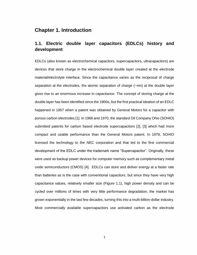
Chapter 1. Introduction
1.1. Electric double layer capacitors (EDLCs) history and
development
EDLCs (also known as electrochemical capacitors, supercapacitors, ultracapacitors) are
devices that store charge in the electrochemical double layer created at the electrode
material/electrolyte interface. Since the capacitance varies as the reciprocal of charge
separation at the electrodes, the atomic separation of charge (~nm) at the double layer
gives rise to an enormous increase in capacitance. The concept of storing charge at the
double layer has been identified since the 1800s, but the first practical ideation of an EDLC
happened in 1957 when a patent was obtained by General Motors for a capacitor with
porous carbon electrodes [1]. In 1966 and 1970, the standard Oil Company Ohio (SOHIO)
submitted patents for carbon based electrode supercapacitors [2], [3] which had more
compact and usable performance than the General Motors patent. In 1978, SOHIO
licensed the technology to the NEC corporation and that led to the first commercial
development of the EDLC under the trademark name “Supercapacitor”. Originally, these
were used as backup power devices for computer memory such as complementary metal
oxide semiconductors (CMOS) [4]. EDLCs can store and deliver energy at a faster rate
than batteries as is the case with conventional capacitors, but since they have very high
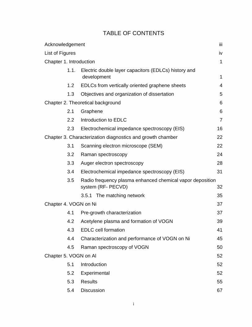
capacitance values, relatively smaller size (Figure 1.1), high power density and can be
cycled over millions of times with very little performance degradation, the market has
grown exponentially in the last few decades, turning this into a multi-billion-dollar industry.
Most commercially available supercapacitors use activated carbon as the electrode
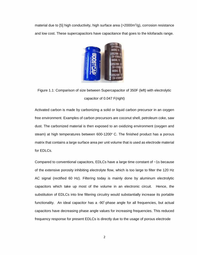
2
material due to [5] high conductivity, high surface area (>2000m2/g), corrosion resistance
and low cost. These supercapacitors have capacitance that goes to the kilofarads range.
Figure 1.1: Comparison of size between Supercapacitor of 350F (left) with electrolytic
capacitor of 0.047 F(right)
Activated carbon is made by carbonizing a solid or liquid carbon precursor in an oxygen
free environment. Examples of carbon precursors are coconut shell, petroleum coke, saw
dust. The carbonized material is then exposed to an oxidizing environment (oxygen and
steam) at high temperatures between 600-1200º C. The finished product has a porous
matrix that contains a large surface area per unit volume that is used as electrode material
for EDLCs.
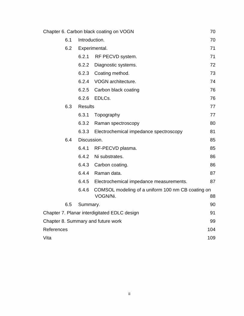
Compared to conventional capacitors, EDLCs have a large time constant of ~1s because
of the extensive porosity inhibiting electrolyte flow, which is too large to filter the 120 Hz
AC signal (rectified 60 Hz). Filtering today is mainly done by aluminum electrolytic
capacitors which take up most of the volume in an electronic circuit. Hence, the
substitution of EDLCs into line filtering circuitry would substantially increase its portable
functionality. An ideal capacitor has a -90º-phase angle for all frequencies, but actual
capacitors have decreasing phase angle values for increasing frequencies. This reduced
frequency response for present EDLCs is directly due to the usage of porous electrode
3
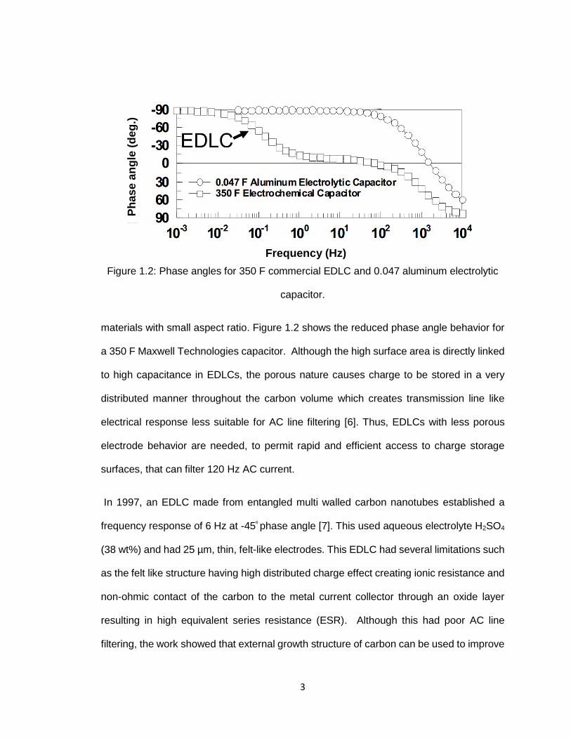
Figure 1.2: Phase angles for 350 F commercial EDLC and 0.047 aluminum electrolytic
capacitor.
materials with small aspect ratio. Figure 1.2 shows the reduced phase angle behavior for
a 350 F Maxwell Technologies capacitor. Although the high surface area is directly linked
to high capacitance in EDLCs, the porous nature causes charge to be stored in a very
distributed manner throughout the carbon volume which creates transmission line like
electrical response less suitable for AC line filtering [6]. Thus, EDLCs with less porous
electrode behavior are needed, to permit rapid and efficient access to charge storage
surfaces, that can filter 120 Hz AC current.
In 1997, an EDLC made from entangled multi walled carbon nanotubes established a
frequency response of 6 Hz at -45º phase angle [7]. This used aqueous electrolyte H2SO4
(38 wt%) and had 25 µm, thin, felt-like electrodes. This EDLC had several limitations such
as the felt like structure having high distributed charge effect creating ionic resistance and
non-ohmic contact of the carbon to the metal current collector through an oxide layer
resulting in high equivalent series resistance (ESR). Although this had poor AC line
filtering, the work showed that external growth structure of carbon can be used to improve
Frequency (Hz)
Ph
as
e a
ng
le (
deg
.)
4
EDLCs as opposed to the usual electrode material such as activated carbon which had
high internal surface area. Other improvements were reported [8], [9]such as electrodes
having multiwall carbon nanotubes deposited onto metal current collectors and
undergoing a furnace treatment to remove surface bonded groups such as oxygen and
hydrogen. These reached 636 Hz frequency at a -45º -phase angle.
1.2 EDLCs from vertically oriented graphene sheets
The central problem of commercial EDLCs is the tradeoff between capacitance and
frequency response. The use of activated carbon has greatly increased the surface area
because of high porosity which provides very high capacitance, but the small pore
diameter and long pore lengths within the carbon black restrict electrolyte movement thus
leading to reduced frequency response. EDLCs made from vertically oriented graphene
nanosheets (VOGN), synthesized by radio frequency plasma enhanced chemical vapor
deposition (RF-PECVD), have been studied and show fast response with efficient filtering
at 120 Hz offering an ideal structure for EDLC electrodes. The open morphology of VOGN
provides high conductance channels of less porosity for efficient ingress and egress of the
electrolyte ions between the vertical nanosheets, thus allowing fast response, minimized
distributed nature of charge and ionic resistance. Electronic resistances of graphene
EDLCs are low because the graphene sheets have extremely high electronic conductivity
and grown from a conductive surface reducing contact resistance. Graphene edge planes
provide capacitance of 50 to 70 µF/cm2 and basal planes, provide capacitance of only ~3
µF/cm2 [10]. These factors provide an EDLC capable of having higher capacitance levels
with minimum series resistance and high-frequency operation.
5
1.3 Objectives and organization of dissertation
The main objective of this dissertation is to characterize vertical oriented graphene sheets
grown on Ni and Al substrates as supercapacitor electrodes. Further, methods to achieve
high frequency response (>120 Hz near -90º phase angle) and low resistance values while
achieving a capacitance as high as possible are presented. Selected substrate materials
Ni and Al have been used as the VOGN platform followed by carbon black coating to
substantially increase the capacitance without significantly reducing the frequency
response at 120 Hz. Chapter 2 introduces the theoretical background behind the electrical
double layer and how its capacitance is measured by using electrochemical impedance
spectroscopy (EIS). Chapter 3 discusses the various characterization tools and the
description of the VOGN growth chamber. The growth, characterization and capacitive
performance of VOGN on Ni and Al EDLCs are discussed in chapters 4 and 5,
respectively. The primary reasons for using Ni and Al as substrate material are also
presented. Chapter 6 focuses on increasing capacitance of the VOGN/Ni EDLCs by using
carbon black coating and chapter 7 presents a novel method of implementing the VOGN
growths in EDLCs for commercial manufacture. Chapter 8 represents a summary of the
work done to date and presents possible directions for future technical advances as well
as development of VOGN EDLCs for commercial production.
6
Chapter 2. Theoretical background
2.1 Graphene
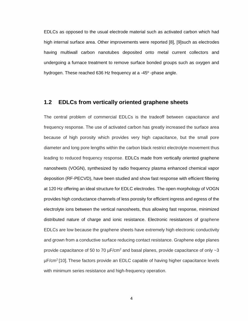
Carbon hybridizations such as sp, sp2 and sp3 have led to the creation of many different
nanostructures. One of the most important is graphene. Graphene is the two-dimensional
arrangement of sp2 bonded carbon atoms in a hexagonal lattice (figure 2.1). Graphene
has been studied theoretically for over 60 years and was first isolated from graphite in
2004 by Geim and Novoselov using the scotch tape method [11]. This led to a vast growth
in graphene research for various fields that led to the 2010 Nobel Prize in Physics awarded
to the aforementioned scientists.
Figure 2.1: Hexagonal structure of graphene, including the orbital hybridization
σ bond
π orbital
C atoms
7
The carbon atoms in a graphene structure have 0.142 nm inter atomic distance. Graphite
is comprised of graphene layers bound together by van der Waals forces in ABA stacking,
0.334 nm apart. The Fermi surface of graphene is given by 6 Dirac cones. Due to these
cones, the delocalized electrons behave as if they have no mass, with relativistic speeds
of around 1/3 the speed of light. Graphene has high thermal and electrical conductivities
(5000 Wm-1k-1 and 6000 Scm-1) [12], [13] as well as high Young’s modulus (1TPa) and
tensile strength (130 GPa) [14].
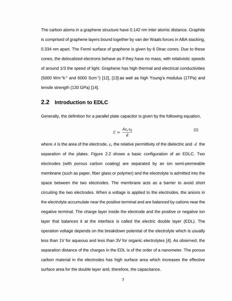
2.2 Introduction to EDLC
Generally, the definition for a parallel plate capacitor is given by the following equation,
𝐶 =
𝐴휀𝑟휀0
𝑑
(1)
where 𝐴 is the area of the electrode, 휀𝑟 the relative permittivity of the dielectric and 𝑑 the
separation of the plates. Figure 2.2 shows a basic configuration of an EDLC. Two
electrodes (with porous carbon coating) are separated by an ion semi-permeable
membrane (such as paper, fiber glass or polymer) and the electrolyte is admitted into the
space between the two electrodes. The membrane acts as a barrier to avoid short
circuiting the two electrodes. When a voltage is applied to the electrodes, the anions in
the electrolyte accumulate near the positive terminal and are balanced by cations near the
negative terminal. The charge layer inside the electrode and the positive or negative ion
layer that balances it at the interface is called the electric double layer (EDL). The
operation voltage depends on the breakdown potential of the electrolyte which is usually
less than 1V for aqueous and less than 3V for organic electrolytes [4]. As observed, the
separation distance of the charges in the EDL is of the order of a nanometer. The porous
carbon material in the electrodes has high surface area which increases the effective
surface area for the double layer and, therefore, the capacitance.
8
Figure 2.2: Diagram of a symmetric EDLC capacitor cell [5]
In conventional parallel plate capacitors, the total capacitance comes from the two
electrodes to make one capacitance value. In EDLCs, there are two double layers on the
anode and cathode electrodes that act as two capacitors in series. So, the total
capacitance is given by,
1
𝐶𝑇𝑜𝑡𝑎𝑙=
1
𝐶𝐴+
1
𝐶𝐶
(2)
𝐶𝑇𝑜𝑡𝑎𝑙 =
𝐶𝐴𝐶𝐶
𝐶𝐴 + 𝐶𝐶
(3)
where CA and CC denote capacitance of the anode and cathode, respectively.
The small separation and the high surface area is what gives rise to the high capacitance
seen in EDLCs. For experimental testing, the capacitance of an individual electrode can
Metal current collector
Ion permeable membrane
Carbon electrode
Electrolyte ions
9
be tested, but in creating a usable capacitor for electronic circuitry, the EDLC must have
two electrodes.
The energy and power density of an EDLC are important criteria when comparing with
other energy storage technologies. The energy density is defined as the total energy
contained within a unit mass or volume of the device whereas power density is a measure
of how much energy per unit mass or volume per unit time. The industry norm is to use
unit mass when discussing power density values. The total energy stored in a capacitor is
given by 1
2𝐶𝑉2. Dividing this by the total mass of the EDLC gives the energy density in
units of Wh/kg. The maximum power delivered is given by the expression 𝑃 =𝑉2
4𝑅𝑆 where
𝑉 is the applied potential and 𝑅𝑆 the equivalent series resistance of the cell. The ESR is
the total effective resistance that comes due to contribution of ionic and electronic
resistances (see section 2.3). The unit for power density is W/kg. One of the main
advantages of an EDLC is that they have a high-power density i.e. high charge/discharge
capability. This can be used as energy buffers that can accept or release high power bursts
for example, in regenerative braking the kinetic energy lost can be stored in an energy
buffer system made from EDLCs. Also, this could be used to quickly release energy that
is needed for vehicle acceleration.
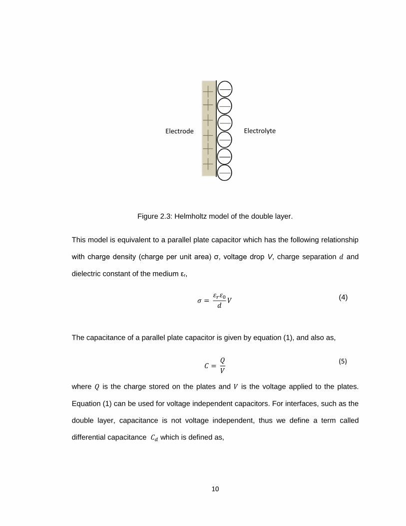
The earliest model for the double layer came from Helmholtz in 1853 [15]. He assumed
that the charge on the solid side is balanced by a layer of opposite charged ions as shown
in figure 2.3. The potential across the double layer drops within one layer of the adsorbed
ions per this model. Other assumptions of this model are no electron transfer reactions at
the electrode-electrolyte interface and the solution contained only electrolyte.
10
Figure 2.3: Helmholtz model of the double layer.
This model is equivalent to a parallel plate capacitor which has the following relationship
with charge density (charge per unit area) σ, voltage drop V, charge separation 𝑑 and
dielectric constant of the medium εr,
𝜎 = 휀𝑟휀0
𝑑𝑉
(4)
The capacitance of a parallel plate capacitor is given by equation (1), and also as,
𝐶 =
𝑄
𝑉
(5)
where 𝑄 is the charge stored on the plates and 𝑉 is the voltage applied to the plates.
Equation (1) can be used for voltage independent capacitors. For interfaces, such as the
double layer, capacitance is not voltage independent, thus we define a term called
differential capacitance 𝐶𝑑 which is defined as,
Electrode Electrolyte
11
𝜕𝜎
𝜕𝑉= 𝐶𝑑 =
휀𝑟휀0
𝑑
(6)
which has units of F/m2
In this model, the capacitance of the double layer appears to be constant for different
applied potentials which is not observed in real double layer systems [16]. Also, the
change in capacitance for different concentrations and types of electrolyte is not clearly
visible in this model which suggested the need for a modification.
Figure 2.4: Gouy-Chapman model
The Helmholtz model was later modified by the Gouy-Chapman model [17], [18]. This
considers the thermal fluctuations according to Boltzmann principle and the non-uniform
distribution of the ions which were considered as point charges, near the double layer
leading the potential across the double layer to gradually decrease. The capacitance
predicted by this model is called the “diffuse layer capacitance”. A theoretical
𝜑x
𝑥
12
understanding of the Gouy-Chapmen model can describe the capacitance of the diffuse
layer (Cdf) as follows,
Let 𝜑x be the potential at x distance in a d thickness dx towards the electrolyte from the
electrode surface. If the bulk concentration in the electrolyte of an ion 𝑖 is 𝐶𝑖0, then the
concentration of the ion 𝑖 at x distance within a length, dx, can be written as a Boltzmann
type of distribution,
𝑐𝑖 = 𝑐𝑖
0𝑒−𝑧𝑖𝑒𝜑𝑥
𝑘𝑇
(7)
where e is the charge of the electron, k, the Boltzmann constant, T, the absolute
temperature and 𝑧𝑖 , the charge (including the sign) of the ion 𝑖 . The total charge density
is given by
𝜌𝑥 = ∑ 𝑐𝑖𝑧𝑖𝑒
𝑖
(8)
where 𝑖 extends over all ions present in the electrolyte.
Then, 𝜌𝑥 can be described by the Poisson’s equation as
∇2𝜑𝑥 = −
𝜌𝑥
휀𝑟휀0
(9)
Combining (7), (8) and (9) gives,
𝑑2𝜑𝑥
𝑑𝑥2=
−ⅇ
ε𝑟ε0∑ c𝑖
0
i
z𝑖ⅇ(
−zi𝑒𝜑𝑥kT
) (10)
13
Integrating this with boundary conditions 𝑑𝜑𝑥
𝑑𝑥 , 𝜑𝑥 = 0 when 𝑥 is large gives,
(
𝑑𝜑𝑥
𝑑𝑥)
2
= 2𝑘𝑇
휀𝑟휀0∑ 𝑐𝑖
0
𝑖
𝑒(−𝑧𝑖𝑒𝜑𝑥
𝑘𝑇) − 1
(11)
For a symmetrical electrolyte (electrolyte with one cationic and one anionic species of
same charge), c𝑖0 = c and 𝑧𝑖 = 𝑧, for all ions 𝑖. Equation (11) becomes;
𝑑𝜑𝑥
𝑑𝑥= − (
8𝑘𝑇𝑐
휀𝑟휀0)
1/2
𝑠𝑖𝑛ℎ (𝑧𝑒𝜑𝑥
2𝑘𝑇)
(12)
By using Gauss law,
𝑞 = ε𝑟ε0 ∮ 𝐸 ∙ 𝑑𝑆
(13)
The field strength E is zero except for the direction perpendicular to the electrode surface.
Considering the charge q on the electrode surface (x=0) this gives,
𝑞 = ε𝑟ε0𝑑𝜑𝑥
𝑑𝑥|
𝑥=0∮ 𝑑𝑆 = ε𝑟ε0 A
𝑑𝜑𝑥
𝑑𝑥|
𝑥=0
(14)
where A is the area of the chosen Gauss surface parallel to the electrode.
Using equation (12) and surface charge density of the electrolyte side 𝜎 = −𝑞/𝐴 ,
14
𝜎 = (8𝑘𝑇ε𝑟ε0c)1/2 sinh (
𝑧𝑒𝜑0
2𝑘𝑇)
(15)
where 𝜑0 is the potential at x=0 relative to the bulk solution or, the drop across the diffuse
layer. Equation (15) gives the differential capacitance of the diffuse layer by,
𝐶𝑑𝑓 = 𝑑𝜎
𝑑𝜑0= (
2𝑧2𝑒2ε𝑟ε0𝑐
𝑘𝑇)
1/2
cosh (𝑧𝑒𝜑0
2𝑘𝑇)
(16)
This model shows that there can be an unlimited increase in double layer capacitance with
increasing 𝜑0 . The failure of this model lies mainly in the assumption that the ions are
considered as point charges. This allows a large amount of ionic charge accumulation
near the electrode and a non-practical separation distance between the ions and the
electrode which constitute the double layer. This is the source from which the anomalous
large capacitance arises. Realistically, ions have a finite size and thus a distance of closest
approach to the electrode.
The modification to the Gouy-Chapman model came from Stern [19] in 1924. This model
considers the double layer as comprised of both Helmholtz layer and Gouy-Chapman
diffuse layer as seen in figure 2.5.
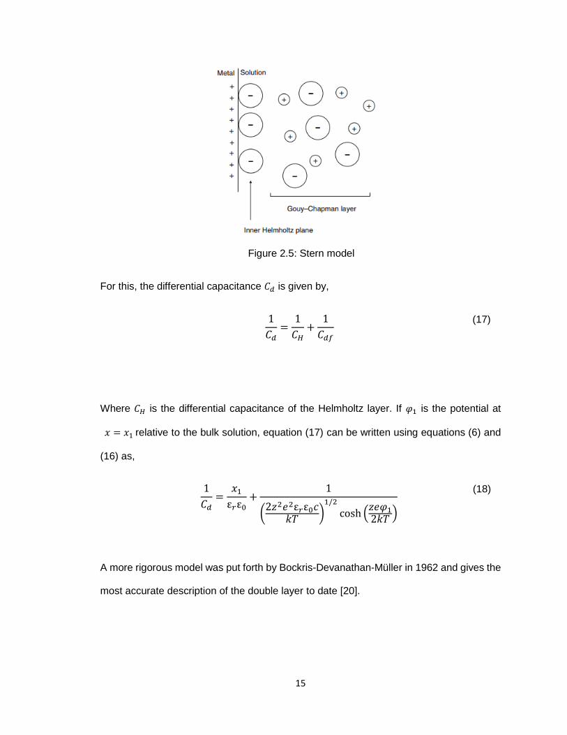
15
Figure 2.5: Stern model
For this, the differential capacitance 𝐶𝑑 is given by,
1
𝐶𝑑=
1
𝐶𝐻+
1
𝐶𝑑𝑓
(17)
Where 𝐶𝐻 is the differential capacitance of the Helmholtz layer. If 𝜑1 is the potential at
𝑥 = 𝑥1 relative to the bulk solution, equation (17) can be written using equations (6) and
(16) as,
1
𝐶𝑑=
𝑥1
ε𝑟ε0+
1
(2𝑧2𝑒2ε𝑟ε0𝑐
𝑘𝑇)
1/2
cosh (𝑧𝑒𝜑1
2𝑘𝑇)
(18)
A more rigorous model was put forth by Bockris-Devanathan-Müller in 1962 and gives the
most accurate description of the double layer to date [20].
16
Figure 2.6: Bockris-Devanathan-Muller model
This model modifies the previous understanding of the double layer by taking into
consideration the dipole interaction of water molecules in the electrolyte. The polarized
water molecules adsorb onto the electrode surface and compete for sites with electrolyte
ions. This layer of ions and molecules closest to the electrode is called the Inner Helmholtz
plane (figure 2.6). Solvated ions can approach the electrode to a certain distance, and
balances, in part, the charge on the electrode. The plane through these hydrated ions is
called the outer Helmholtz plane. The diffuse layer defined in the Gouy-Chapman model
lies beyond the outer Helmholtz layer. This model takes into account the overall effect
from all three layers and this updated version is the most fitting explanation for the
behavior of the double layer.
2.3 Electrochemical impedance spectroscopy (EIS)
The capacitive behavior of an EDLC cell can be accurately obtained by using EIS testing
as opposed to directly interpreting the behavior of the double layer. There are other
methods such as potentiostatic, Galvanostatic, sweep voltammetry and disk
electrochemistry [21]. All these methods use large perturbations to the system, then record
1 = Inner layer
2 = Outer layer
3 = Gouy-Chapman layer
4 = Solvated cation
17
the output responses. The EIS method uses an alternating signal with small amplitude to
perturb the system. There are three diagram types of impedance behavior as a function
of frequency. They are,
1. Capacitance vs frequency plot (capacitance at zero Hertz gives the DC
capacitance of the cell).
2. Imaginary vs real component of impedance plot (Nyquist plot or complex plane
plot)
3. Phase angle vs frequency plot (Bode plot).
When we consider the impedance of a capacitor 𝑍𝐶 , it can be shown like 𝑍′(ω) + i𝑍"(ω)
where Z’ is the real component of the impedance and Z” is the imaginary component. The
voltage across a capacitor is given as a time dependent function as,
𝑉(𝑡) =
𝑄(𝑡)
𝐶=
𝐼(𝑡)𝑡
𝐶
(19)
𝑑𝑉(𝑡)
𝑑𝑡=
1
𝐶[𝐼(𝑡) +
𝑡 𝑑𝐼(𝑡)
𝑑𝑡 ]
(20)
If current 𝐼(𝑡) is held constant,
𝑑𝑉(𝑡)
𝑑𝑡=
𝐼(𝑡)
𝐶, sincⅇ
𝑑𝐼(𝑡)
𝑑𝑡= 0
(21)
Impedance is then given by,
𝑍𝐶 =
𝑉(𝑡)
𝐼(𝑡)=
𝑉(𝑡)
𝐶𝑑𝑉(𝑡)
𝑑𝑡
=𝑉0𝑒𝑖𝜔𝑡
𝐶𝑖𝜔𝑉0𝑒𝑖𝜔𝑡
(22)
𝑍𝐶 =
−𝑖
2𝜋𝑓𝐶
(23)
where f is the frequency and C is the capacitance.
18
The equivalent series resistance (ESR) is the series resistance that occurs in capacitors
which shows the non-ideal behavior of the system. Actual capacitors do not show pure
capacitive behavior as shown in equation 23. Factors that contribute to the ESR of an
EDLC are, electrolyte resistance, electronic resistance (contact resistance between
carbon electrodes and the metal current collector mostly through an oxide and the intrinsic
resistance of the current collector, carbon electrodes and external lead contacts) and
membrane (between the two electrodes) resistance. The electrolyte resistance would be
affected by the following factors; concentration of ions or mobile charge carriers’ and the
ionic mobilities of the disassociated ions.
In the EIS technique the system is initially at a steady state under a constant DC potential.
Then, the system is perturbed by using an AC signal of small amplitude. This enables the
different processes that govern the current flow through the system, to go back to the
steady state according to those different time constants. For example, high rate
processes, such as charge transfer reactions are active at high frequencies, and low rate
processes, such as mass diffusion, are active at low frequencies. The perturbation signal,
𝛿𝐸(𝜔), is applied to the constant potential, 𝐸𝑠, at steady state where the steady state
current is 𝐼𝑠. So, the potential and current can be written as,
𝐸 = 𝐸𝑠 + 𝛿𝐸(𝜔) 𝑤ℎ𝑒𝑟𝑒 𝛿𝐸(𝜔) = |𝛿𝐸(𝜔)| 𝑒−𝑖𝜔𝑡 (24)
𝐼 = 𝐼𝑠 + 𝛿𝐼(𝜔) 𝑤ℎ𝑒𝑟𝑒 𝛿𝐼(𝜔) = |𝛿𝐼(𝜔)| 𝑒(−𝑖𝜔𝑡+𝛷)
(25)
The 𝛷 is the phase angle between the current and the potential.
The impedance is defined as,
𝑍(𝜔) =
𝛿𝐸(𝜔)
𝛿𝐼(𝜔)= 𝑍′(𝜔) + 𝑖𝑍"(𝜔)
(26)
19
When the EIS equipment is run for a range of frequencies, Z′(ω) and , Z"(ω) component
values are given as the output. From these values, we can generate the required
diagrams.
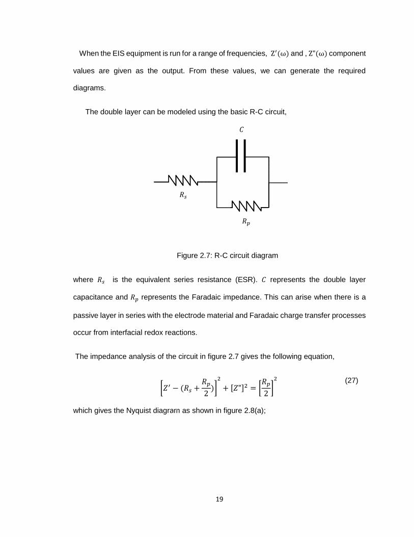
The double layer can be modeled using the basic R-C circuit,
Figure 2.7: R-C circuit diagram
where 𝑅𝑠 is the equivalent series resistance (ESR). 𝐶 represents the double layer
capacitance and 𝑅𝑝 represents the Faradaic impedance. This can arise when there is a
passive layer in series with the electrode material and Faradaic charge transfer processes
occur from interfacial redox reactions.
The impedance analysis of the circuit in figure 2.7 gives the following equation,
[𝑍′ − (𝑅𝑠 +
𝑅𝑝
2)]
2
+ [𝑍"]2 = [𝑅𝑝
2]
2
(27)
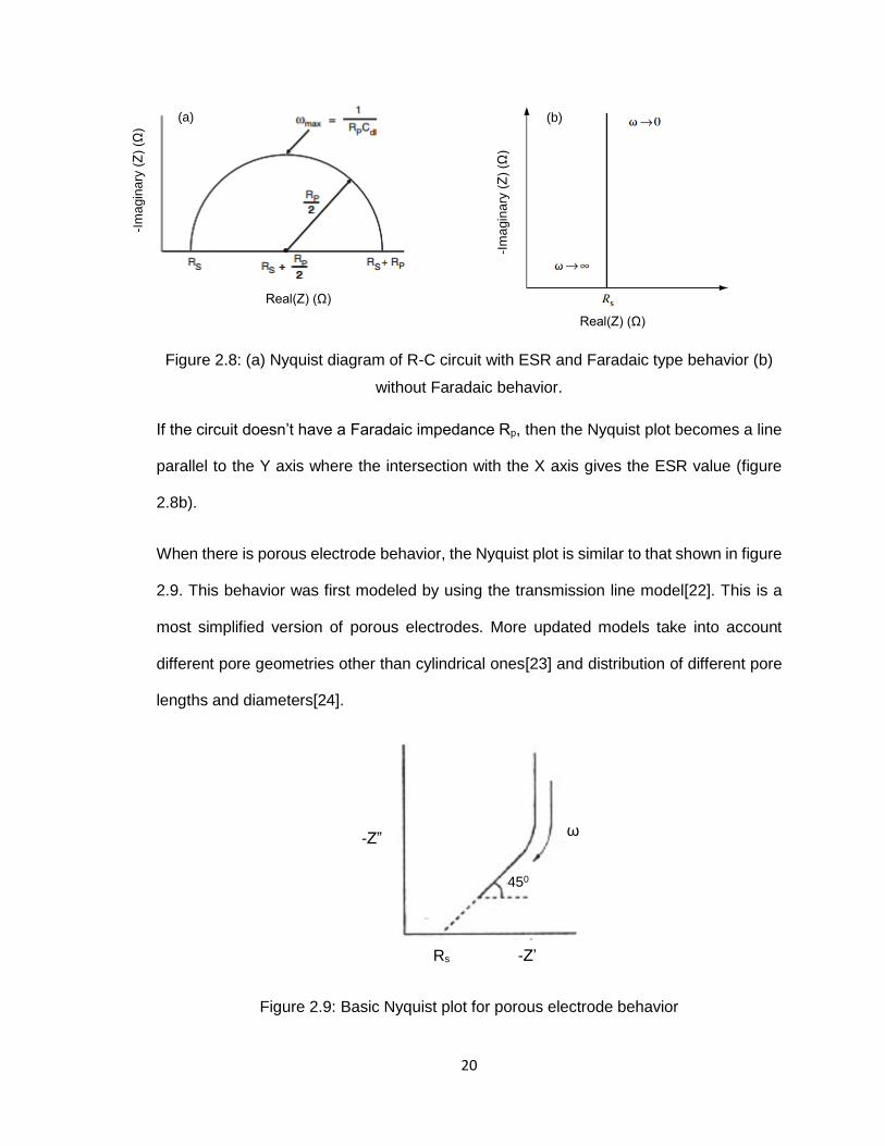
which gives the Nyquist diagram as shown in figure 2.8(a);
𝑅𝑠
𝑅𝑝
𝐶
20
Figure 2.8: (a) Nyquist diagram of R-C circuit with ESR and Faradaic type behavior (b)
without Faradaic behavior.
If the circuit doesn’t have a Faradaic impedance Rp, then the Nyquist plot becomes a line
parallel to the Y axis where the intersection with the X axis gives the ESR value (figure
2.8b).
When there is porous electrode behavior, the Nyquist plot is similar to that shown in figure
2.9. This behavior was first modeled by using the transmission line model[22]. This is a
most simplified version of porous electrodes. More updated models take into account
different pore geometries other than cylindrical ones[23] and distribution of different pore
lengths and diameters[24].
Figure 2.9: Basic Nyquist plot for porous electrode behavior
Real(Z) (Ω)
-Im
agin
ary
(Z
) (Ω
)
Real(Z) (Ω)
-Im
agin
ary
(Z
) (Ω
)
(b) (a)
ω
-Z”
-Z’ Rs
450
21
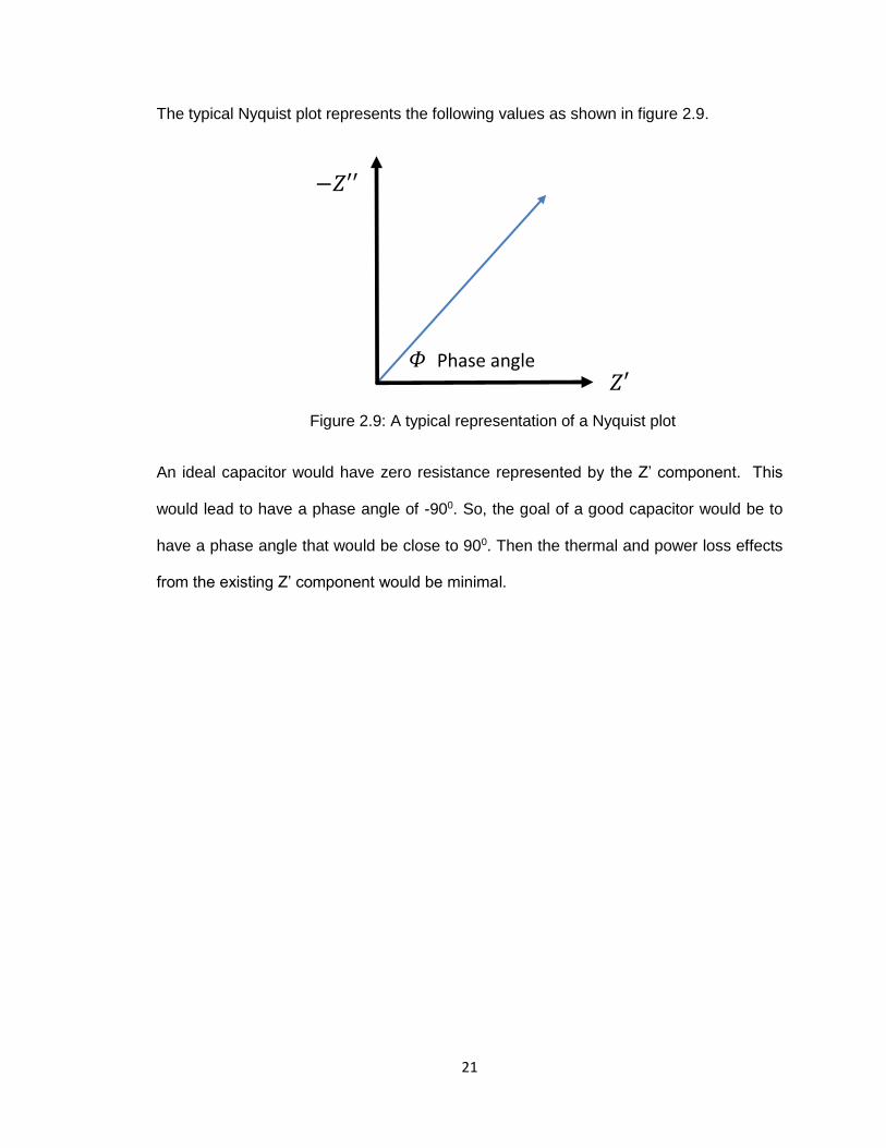
The typical Nyquist plot represents the following values as shown in figure 2.9.
Figure 2.9: A typical representation of a Nyquist plot
An ideal capacitor would have zero resistance represented by the Z’ component. This
would lead to have a phase angle of -900. So, the goal of a good capacitor would be to
have a phase angle that would be close to 900. Then the thermal and power loss effects
from the existing Z’ component would be minimal.
𝛷 Phase angle 𝑍′
−𝑍′′
22
Chapter 3. Characterization diagnostics and growth
chamber
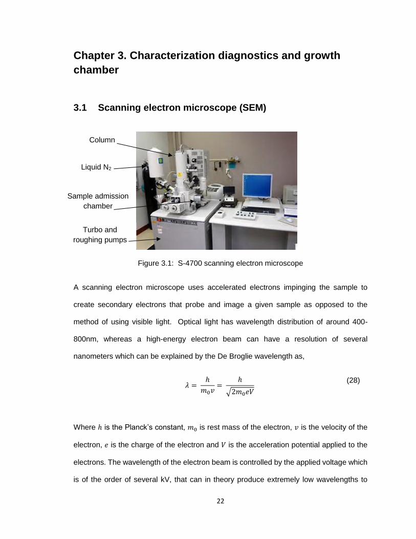
3.1 Scanning electron microscope (SEM)
Figure 3.1: S-4700 scanning electron microscope
A scanning electron microscope uses accelerated electrons impinging the sample to
create secondary electrons that probe and image a given sample as opposed to the
method of using visible light. Optical light has wavelength distribution of around 400-
800nm, whereas a high-energy electron beam can have a resolution of several
nanometers which can be explained by the De Broglie wavelength as,
𝜆 =
ℎ
𝑚0𝑣=
ℎ
√2𝑚0𝑒𝑉
(28)
Where ℎ is the Planck’s constant, 𝑚0 is rest mass of the electron, 𝑣 is the velocity of the
electron, 𝑒 is the charge of the electron and 𝑉 is the acceleration potential applied to the
electrons. The wavelength of the electron beam is controlled by the applied voltage which
is of the order of several kV, that can in theory produce extremely low wavelengths to
Liquid N2
Column
Sample admission
chamber
Turbo and
roughing pumps
23
produce very high-resolution images. But instrument limitations such as aberration and
size of the focused electron beam determine the ultimate resolution of the microscope.
Figure 3.2 shows the basic illustration of how an SEM works. The electron beam is
produced by a thermionic, Schottky or field emission type of electron source. The beam is
focused using electromagnetic lenses and when the beam strikes the sample specimen,
backscattered electrons (BSEs), Auger electrons, secondary electrons (SEs) and X-rays
are created. SEs and BSEs are used to create the image of the specimen and X-rays are
used to identify the composition of the specimen. Mainly, SEs are used to get the
morphology and the topography of the specimen while BSEs are most valuable to image
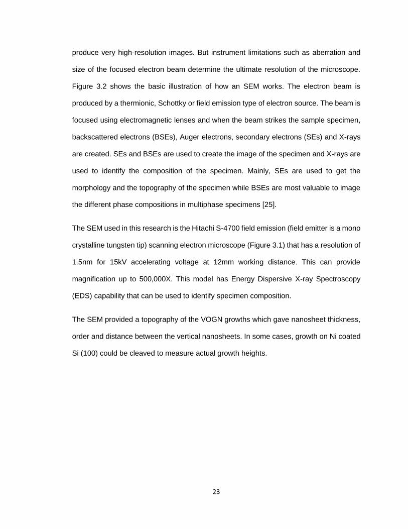
the different phase compositions in multiphase specimens [25].
The SEM used in this research is the Hitachi S-4700 field emission (field emitter is a mono
crystalline tungsten tip) scanning electron microscope (Figure 3.1) that has a resolution of
1.5nm for 15kV accelerating voltage at 12mm working distance. This can provide
magnification up to 500,000X. This model has Energy Dispersive X-ray Spectroscopy
(EDS) capability that can be used to identify specimen composition.
The SEM provided a topography of the VOGN growths which gave nanosheet thickness,
order and distance between the vertical nanosheets. In some cases, growth on Ni coated
Si (100) could be cleaved to measure actual growth heights.
24
Figure 3.2: Schematic of internal mechanism of a typical scanning electron microscope
3.2 Raman spectroscopy
Raman spectroscopy is a technique that uses inelastic scattering of monochromatic light
for a given sample to provide a method to identify the chemical structure for sample
identification and quantification. When photons are incident on a material surface, most
undergo elastic scattering (Rayleigh scattering). A small fraction of photons (1 in 106-108)
[26] undergo inelastic scattering. This is called the Raman effect and was discovered by
C.V Raman in 1928. Raman scattering is comprised of Stokes and anti-Stokes process.
Raman spectroscopy uses a monochromatic incident beam of radiation (typically, a laser)
to irradiate the sample. The incident light polarizes the electron cloud around the nuclei to
form a “virtual state” of the molecule that is unstable and has a short lifetime. Molecules
that undergo this type of polarizability are called “Raman active”. This quickly relaxes and
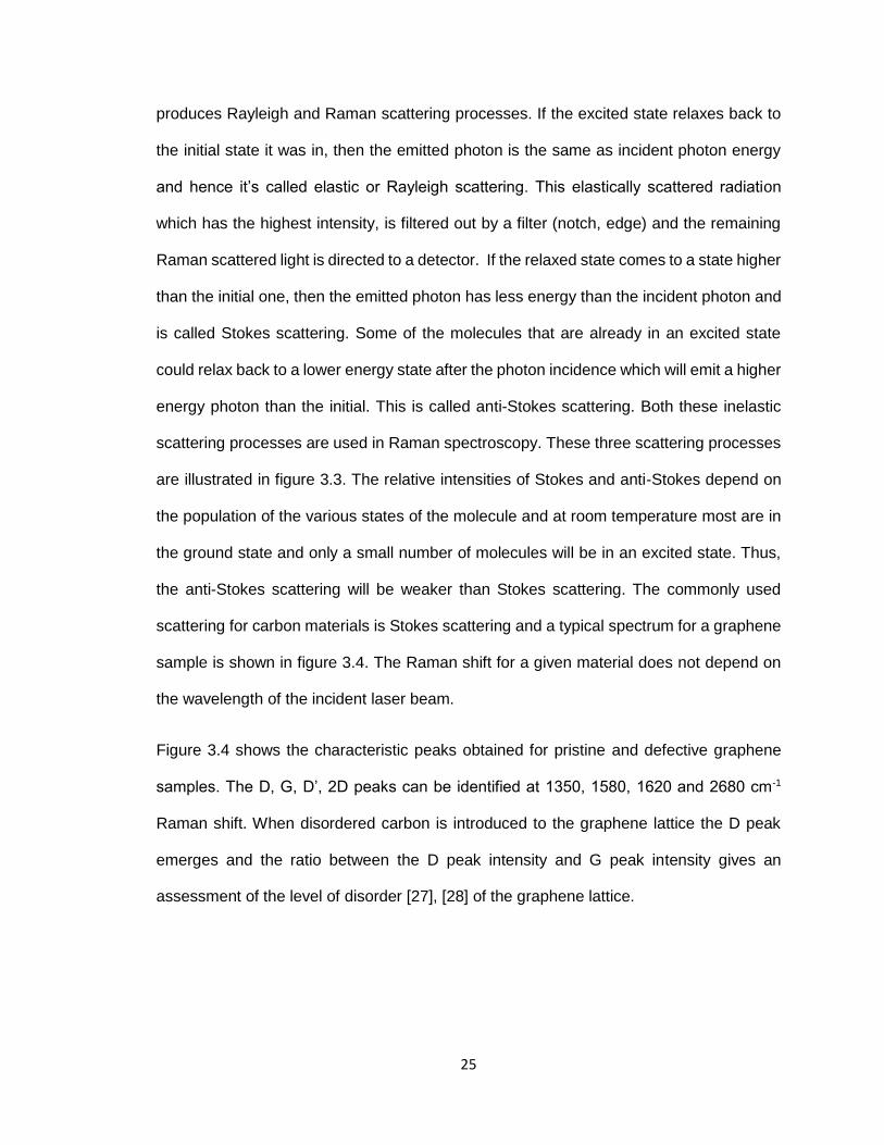
25
produces Rayleigh and Raman scattering processes. If the excited state relaxes back to
the initial state it was in, then the emitted photon is the same as incident photon energy
and hence it’s called elastic or Rayleigh scattering. This elastically scattered radiation
which has the highest intensity, is filtered out by a filter (notch, edge) and the remaining
Raman scattered light is directed to a detector. If the relaxed state comes to a state higher
than the initial one, then the emitted photon has less energy than the incident photon and
is called Stokes scattering. Some of the molecules that are already in an excited state
could relax back to a lower energy state after the photon incidence which will emit a higher
energy photon than the initial. This is called anti-Stokes scattering. Both these inelastic
scattering processes are used in Raman spectroscopy. These three scattering processes
are illustrated in figure 3.3. The relative intensities of Stokes and anti-Stokes depend on
the population of the various states of the molecule and at room temperature most are in
the ground state and only a small number of molecules will be in an excited state. Thus,
the anti-Stokes scattering will be weaker than Stokes scattering. The commonly used
scattering for carbon materials is Stokes scattering and a typical spectrum for a graphene
sample is shown in figure 3.4. The Raman shift for a given material does not depend on
the wavelength of the incident laser beam.
Figure 3.4 shows the characteristic peaks obtained for pristine and defective graphene
samples. The D, G, D’, 2D peaks can be identified at 1350, 1580, 1620 and 2680 cm-1
Raman shift. When disordered carbon is introduced to the graphene lattice the D peak
emerges and the ratio between the D peak intensity and G peak intensity gives an
assessment of the level of disorder [27], [28] of the graphene lattice.
26
Figure 3.3: The orange and blue lines represent the Raman process. The red represents
Rayleigh scattering
Figure 3.4: Raman spectra of pristine (top) and disordered (bottom)graphene.[29]
27
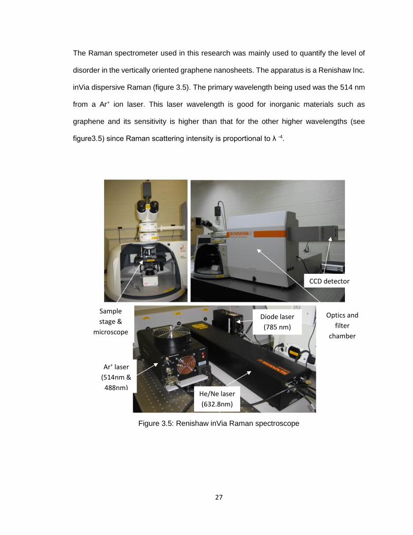
The Raman spectrometer used in this research was mainly used to quantify the level of
disorder in the vertically oriented graphene nanosheets. The apparatus is a Renishaw Inc.
inVia dispersive Raman (figure 3.5). The primary wavelength being used was the 514 nm
from a Ar+ ion laser. This laser wavelength is good for inorganic materials such as
graphene and its sensitivity is higher than that for the other higher wavelengths (see
figure3.5) since Raman scattering intensity is proportional to λ -4.
Figure 3.5: Renishaw inVia Raman spectroscope
Sample
stage &
microscope
Optics and
filter
chamber
CCD detector
Ar+ laser
(514nm &
488nm) He/Ne laser
(632.8nm)
Diode laser
(785 nm)
28
3.3 Auger electron spectroscopy
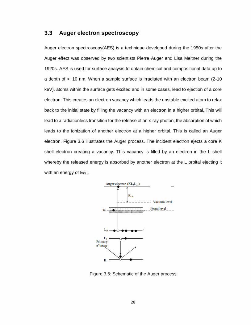
Auger electron spectroscopy(AES) is a technique developed during the 1950s after the
Auger effect was observed by two scientists Pierre Auger and Lisa Meitner during the
1920s. AES is used for surface analysis to obtain chemical and compositional data up to
a depth of <~10 nm. When a sample surface is irradiated with an electron beam (2-10
keV), atoms within the surface gets excited and in some cases, lead to ejection of a core
electron. This creates an electron vacancy which leads the unstable excited atom to relax
back to the initial state by filling the vacancy with an electron in a higher orbital. This will
lead to a radiationless transition for the release of an x-ray photon, the absorption of which
leads to the ionization of another electron at a higher orbital. This is called an Auger
electron. Figure 3.6 illustrates the Auger process. The incident electron ejects a core K
shell electron creating a vacancy. This vacancy is filled by an electron in the L shell
whereby the released energy is absorbed by another electron at the L orbital ejecting it
with an energy of EKLL.
Figure 3.6: Schematic of the Auger process
29
Energy analysis of the emitted electrons due to the irradiation of electron beams is
achieved by a double pass cylindrical mirror analyzer, PHI GAR 255 (angle resolved). The
kinetic energies of Auger electrons are determined by the incident beam energy according
to the following equation[30].
𝐸𝐴𝐵𝐶(z) = E𝐴 (z) − E𝐵(z) − E𝐶(z) − H + 𝑅𝑖𝑛 + 𝑅𝑒𝑥 − φ
(29)
where 𝐸𝐴𝐵𝐶(z) is the kinetic energy of an Auger electron with arbitrary transition ABC (e.g.
KLL) of an atom with atomic number z. E𝐴−𝐶 (z) represents electron binding energies of
arbitrary levels A, B and C. The hole-hole interaction energy of the final two-hole state is
given by H. 𝑅𝑖𝑛 , 𝑅𝑒𝑥 gives the intra- atomic and extra- atomic relaxation energies. This
accounts for the contraction of the electron orbitals due to the presence of a core hole.
The work function for the material is given by φ. Measurement of the emitted electron
kinetic energies provides a unique energy signature which provides compositional
information for each element examined. AES is a surface specific technique, since kinetic
energies of the Auger electrons are lost due to inelastic collisions when they move through
a solid material. The average distance traveled before such a collision, the inelastic mean
free path, is only 2-6 monolayers. The energy distribution of the electrons (𝑁(𝐸)) is plotted
Vs electron kinetic energy. This spectrum is differentiated with respect to kinetic energy,
𝑑𝑁(𝐸)
𝑑𝐸 and plotted against kinetic energy to obtain the characteristic Auger spectra.
The Auger spectrometer (Perkin-Elmer PHI590) used in this work for elemental analyses
of carbon nanosheets is part of the multifunctional surface analysis system at the College
of William and Mary (Figure 3.7b). The base pressure of the chamber is ~ 10-11 Torr. Using
a 3kV, 0.5 µA electron beam and scanning rate of 1eV/S, the detection limit is <1 atomic
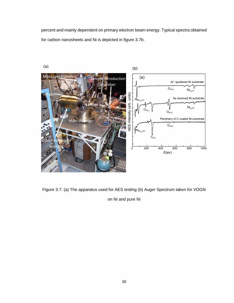
30
percent and mainly dependent on primary electron beam energy. Typical spectra obtained
for carbon nanosheets and Ni is depicted in figure 3.7b.
Figure 3.7: (a) The apparatus used for AES testing (b) Auger Spectrum taken for VOGN
on Ni and pure Ni
(b) (a)
Ion gun
Sample introduction
chamber
Cylindrical mirror
analyzer
Main chamber
Mass spectrometer
31
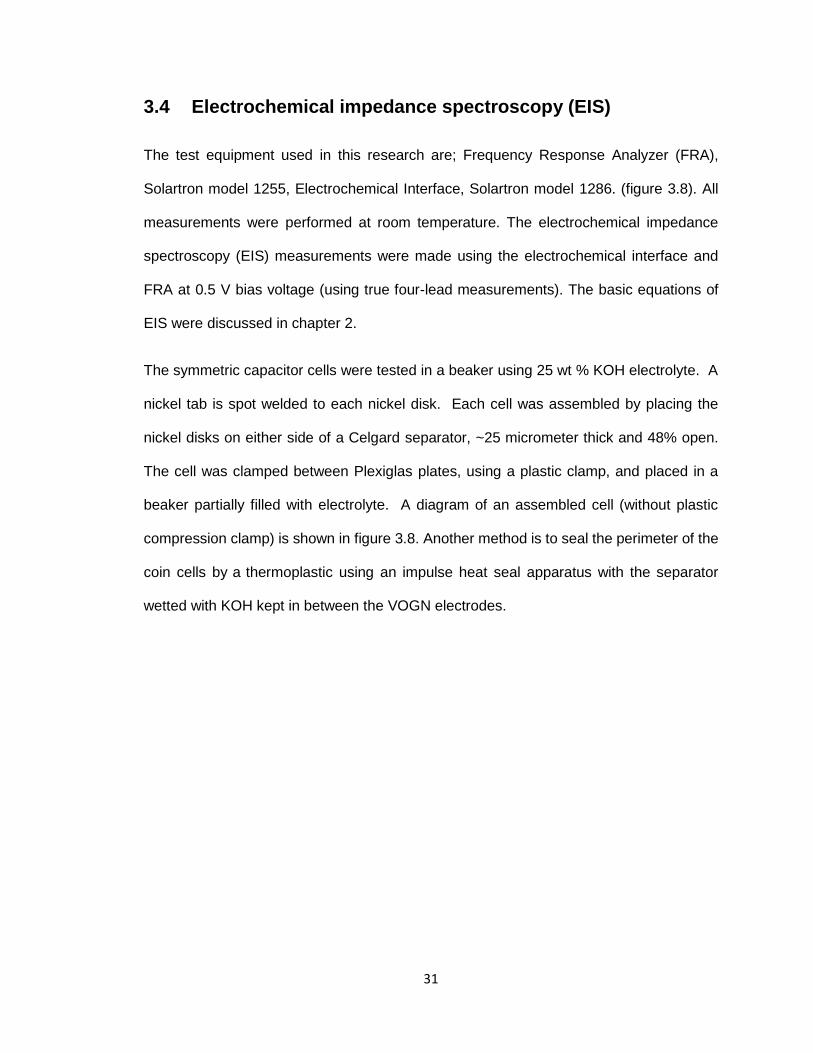
3.4 Electrochemical impedance spectroscopy (EIS)
The test equipment used in this research are; Frequency Response Analyzer (FRA),
Solartron model 1255, Electrochemical Interface, Solartron model 1286. (figure 3.8). All
measurements were performed at room temperature. The electrochemical impedance
spectroscopy (EIS) measurements were made using the electrochemical interface and
FRA at 0.5 V bias voltage (using true four-lead measurements). The basic equations of
EIS were discussed in chapter 2.
The symmetric capacitor cells were tested in a beaker using 25 wt % KOH electrolyte. A
nickel tab is spot welded to each nickel disk. Each cell was assembled by placing the
nickel disks on either side of a Celgard separator, ~25 micrometer thick and 48% open.
The cell was clamped between Plexiglas plates, using a plastic clamp, and placed in a
beaker partially filled with electrolyte. A diagram of an assembled cell (without plastic
compression clamp) is shown in figure 3.8. Another method is to seal the perimeter of the
coin cells by a thermoplastic using an impulse heat seal apparatus with the separator
wetted with KOH kept in between the VOGN electrodes.
32
Figure 3.8: (a): Coin cell testing procedure for VOGN on Ni coin cells. Tab 1 and 2 are
connected to the above-mentioned equipment terminals. (b) Frequency Response
Analyzer (FRA), Solartron model 1255
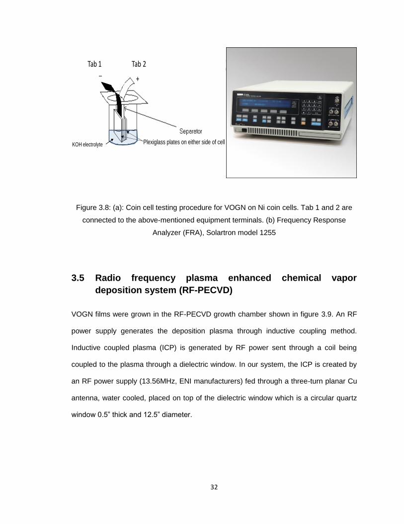
3.5 Radio frequency plasma enhanced chemical vapor
deposition system (RF-PECVD)
VOGN films were grown in the RF-PECVD growth chamber shown in figure 3.9. An RF
power supply generates the deposition plasma through inductive coupling method.
Inductive coupled plasma (ICP) is generated by RF power sent through a coil being
coupled to the plasma through a dielectric window. In our system, the ICP is created by
an RF power supply (13.56MHz, ENI manufacturers) fed through a three-turn planar Cu
antenna, water cooled, placed on top of the dielectric window which is a circular quartz
window 0.5” thick and 12.5” diameter.
Carbon disk is placed between
Coated silver and separator
Coated SilverCoated Silver Carbon disk is placed between
Coated silver and separator
Coated Silver Carbon disk is placed between
Coated silver and separator
Carbon disk is placed between
Coated silver and separator
Coated SilverCoated Silver
Plexiglass plates on either side of cell
Carbon disk is placed between
Coated silver and separator
Coated SilverCoated Silver Carbon disk is placed between
Coated silver and separator
Coated Silver Carbon disk is placed between
Coated silver and separator
Carbon disk is placed between
Coated silver and separator
Coated SilverCoated Silver
Plexiglass plates on either side of cell
Tab 1 Tab 2
+
KOH electrolyte
33
Figure 3.9: Schematic of the RF-PECVD system
Figure 3.10: (a) The RF power supply and control unit (b) The RF-PECVD matching
network. (c) RF antenna top hat enclosure. (d) RF-PECVD vacuum growth chamber.
Heater power
supply
Aluminum
top hat
Ar
H2
C2H2
Mass flow controllers
Copper antenna
a
b c
d
34
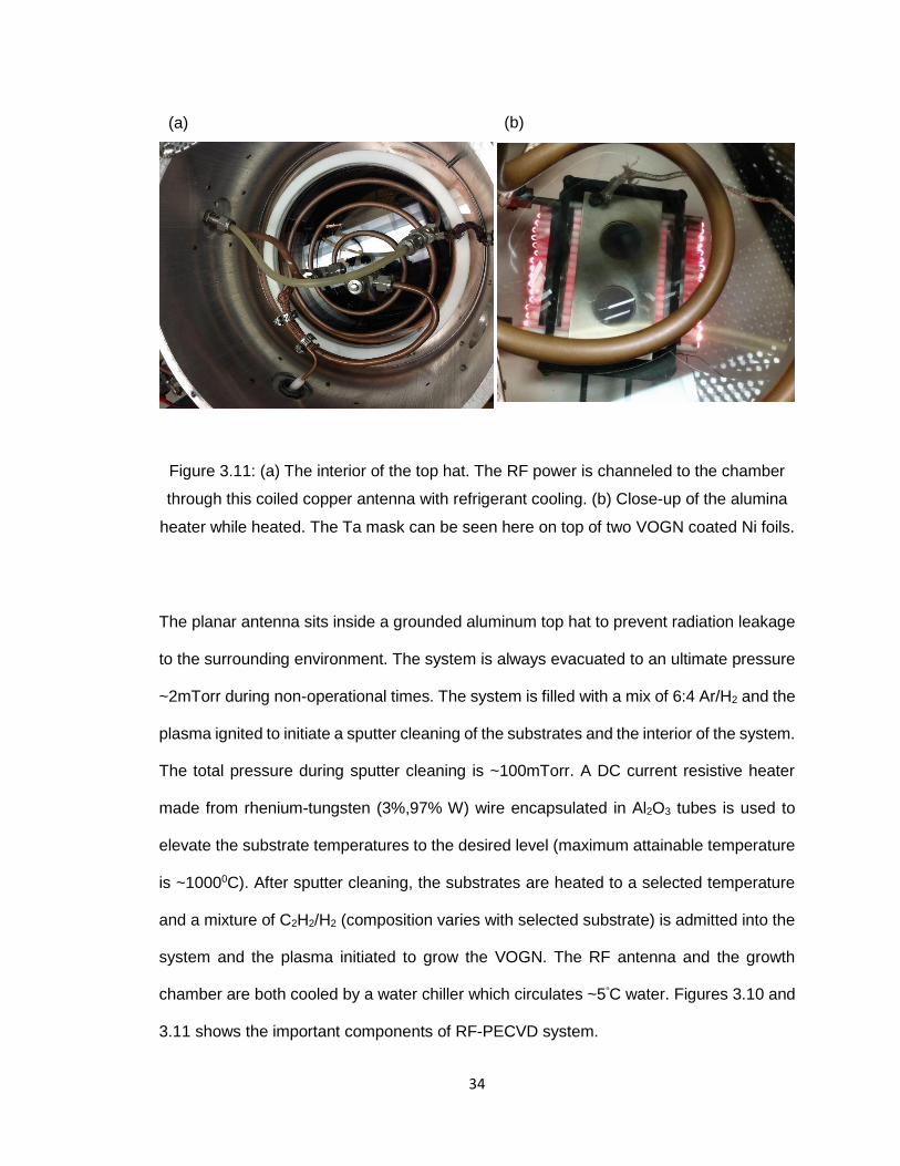
Figure 3.11: (a) The interior of the top hat. The RF power is channeled to the chamber
through this coiled copper antenna with refrigerant cooling. (b) Close-up of the alumina
heater while heated. The Ta mask can be seen here on top of two VOGN coated Ni foils.
The planar antenna sits inside a grounded aluminum top hat to prevent radiation leakage
to the surrounding environment. The system is always evacuated to an ultimate pressure
~2mTorr during non-operational times. The system is filled with a mix of 6:4 Ar/H2 and the
plasma ignited to initiate a sputter cleaning of the substrates and the interior of the system.
The total pressure during sputter cleaning is ~100mTorr. A DC current resistive heater
made from rhenium-tungsten (3%,97% W) wire encapsulated in Al2O3 tubes is used to
elevate the substrate temperatures to the desired level (maximum attainable temperature
is ~10000C). After sputter cleaning, the substrates are heated to a selected temperature
and a mixture of C2H2/H2 (composition varies with selected substrate) is admitted into the
system and the plasma initiated to grow the VOGN. The RF antenna and the growth
chamber are both cooled by a water chiller which circulates ~5ºC water. Figures 3.10 and
3.11 shows the important components of RF-PECVD system.
(b) (a)
35
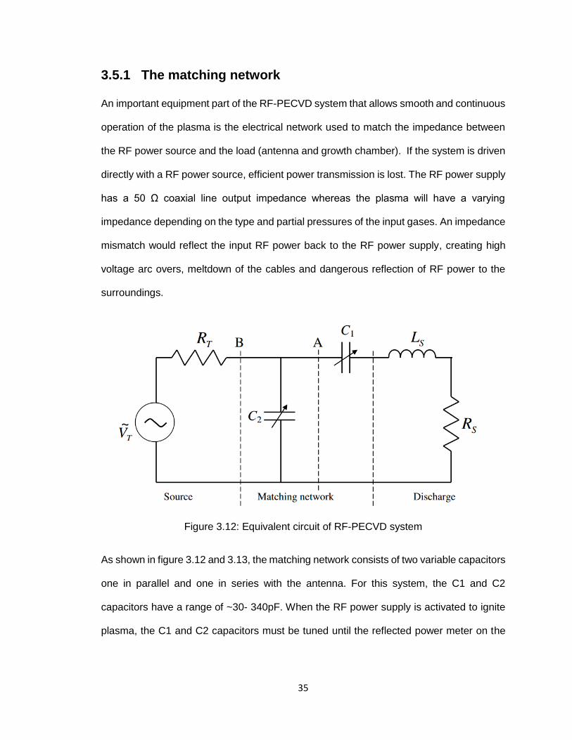
3.5.1 The matching network
An important equipment part of the RF-PECVD system that allows smooth and continuous
operation of the plasma is the electrical network used to match the impedance between
the RF power source and the load (antenna and growth chamber). If the system is driven
directly with a RF power source, efficient power transmission is lost. The RF power supply
has a 50 Ω coaxial line output impedance whereas the plasma will have a varying
impedance depending on the type and partial pressures of the input gases. An impedance
mismatch would reflect the input RF power back to the RF power supply, creating high
voltage arc overs, meltdown of the cables and dangerous reflection of RF power to the
surroundings.
Figure 3.12: Equivalent circuit of RF-PECVD system
As shown in figure 3.12 and 3.13, the matching network consists of two variable capacitors
one in parallel and one in series with the antenna. For this system, the C1 and C2
capacitors have a range of ~30- 340pF. When the RF power supply is activated to ignite
plasma, the C1 and C2 capacitors must be tuned until the reflected power meter on the
36
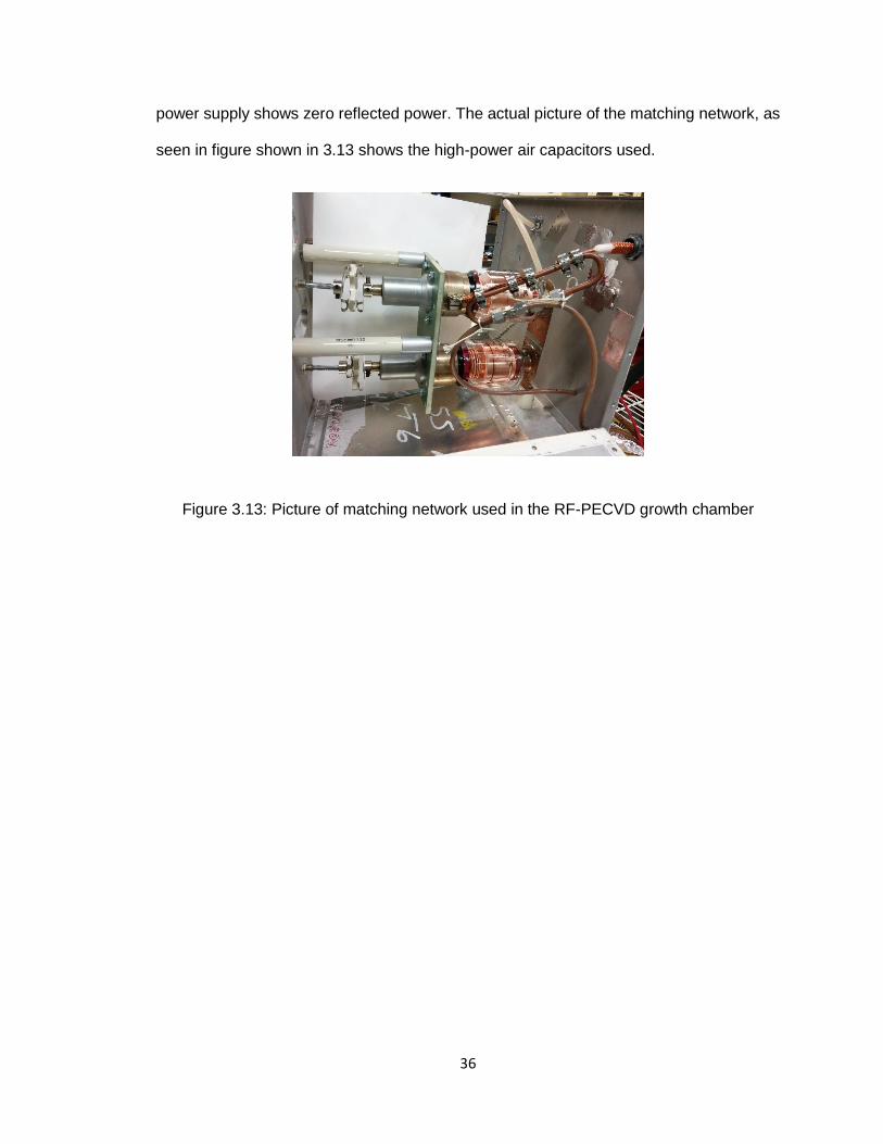
power supply shows zero reflected power. The actual picture of the matching network, as
seen in figure shown in 3.13 shows the high-power air capacitors used.
Figure 3.13: Picture of matching network used in the RF-PECVD growth chamber
37
Chapter 4. VOGN on Ni
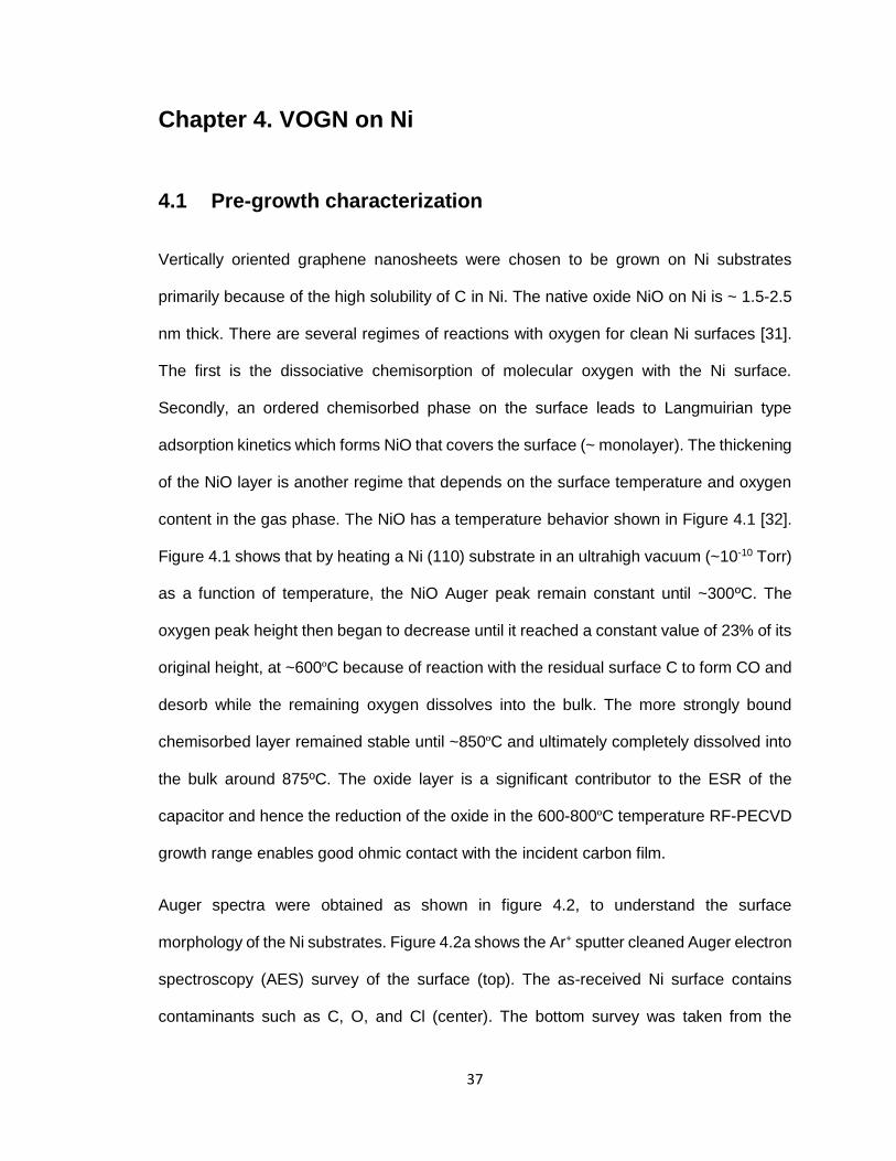
4.1 Pre-growth characterization
Vertically oriented graphene nanosheets were chosen to be grown on Ni substrates
primarily because of the high solubility of C in Ni. The native oxide NiO on Ni is ~ 1.5-2.5
nm thick. There are several regimes of reactions with oxygen for clean Ni surfaces [31].
The first is the dissociative chemisorption of molecular oxygen with the Ni surface.
Secondly, an ordered chemisorbed phase on the surface leads to Langmuirian type
adsorption kinetics which forms NiO that covers the surface (~ monolayer). The thickening
of the NiO layer is another regime that depends on the surface temperature and oxygen
content in the gas phase. The NiO has a temperature behavior shown in Figure 4.1 [32].
Figure 4.1 shows that by heating a Ni (110) substrate in an ultrahigh vacuum (~10-10 Torr)
as a function of temperature, the NiO Auger peak remain constant until ~300ºC. The
oxygen peak height then began to decrease until it reached a constant value of 23% of its
original height, at ~600ºC because of reaction with the residual surface C to form CO and
desorb while the remaining oxygen dissolves into the bulk. The more strongly bound
chemisorbed layer remained stable until ~850ºC and ultimately completely dissolved into
the bulk around 875ºC. The oxide layer is a significant contributor to the ESR of the
capacitor and hence the reduction of the oxide in the 600-800ºC temperature RF-PECVD
growth range enables good ohmic contact with the incident carbon film.
Auger spectra were obtained as shown in figure 4.2, to understand the surface
morphology of the Ni substrates. Figure 4.2a shows the Ar+ sputter cleaned Auger electron
spectroscopy (AES) survey of the surface (top). The as-received Ni surface contains
contaminants such as C, O, and Cl (center). The bottom survey was taken from the
38
periphery of the substrate that was covered by the Ta mask during deposition. Although,
visual inspection of that area shows the Ni surface with slight discoloration and no
apparent growth of VOGN, the predominant signal from the periphery is carbon, not nickel.
A slight oxygen signal from re-exposure to the atmosphere can also be observed. This
suggests that the substrate temperature during deposition was sufficient to cause carbon
to dissolve into the bulk and diffuse radially outward from the central deposition region into
the uncoated mask-protected periphery. Figure 4.2b shows the depth profile of the ratio
of CKLL to NiMVV intensities in this uncoated region. This area was inspected by sputtering
with an Ar+ beam for 10.5 hrs, taking an AES spectrum every 30 minutes to calculate the
C to Ni ratio. This sputtering led to a depth of ∼1 μm where the C signal could still be
detected. Eventually, the ratio approached a constant level associated with C saturation
in the Ni bulk. This suggests that the carbon species in the plasma adsorbed and then
Figure 4.1: Normalized oxygen Auger peak to peak height vs temperature [32]. The
decrease in the ratio at ~300ºC is the loss of surface O by reaction with surface C and
the subsequent dissolution of the O into the Ni bulk.
39
dissolved well into Ni substrates, thus producing good ohmic bonding between the VOGN
and the Ni substrate. The AES survey of VOGN films shows only the carbon “dolphin peak”
at 270 eV with no other elements. These results indicate the high purity of the VOGN (<1%
contaminant).
Figure 4.2: Auger surveys of the Ni substrate sputter cleaned (top) and as received
(center), and the mask-covered periphery Ni outside the center VOGN region (bottom).
(b) Depth profile of the C/Ni intensity ratio measured in the periphery of VOGN growth
that shows C diffusion into the Ni substrate and laterally into the uncoated region of the
Ni periphery [33].
4.2 Acetylene plasma and formation of VOGN
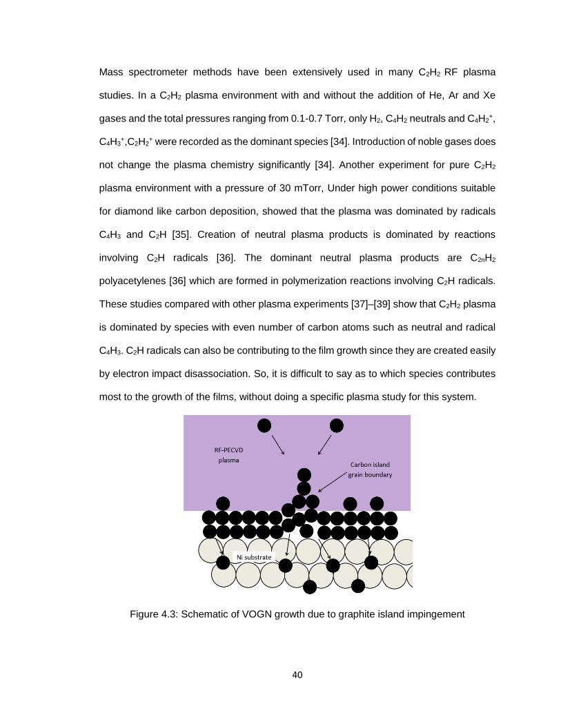
The initial VOGN growth occurs due to Volmer Weber planar type of two-dimensional
graphitic islands on the Ni substrate. These graphitic islands ultimately impinge on each
other, leading to grain boundary regions where further deposition pushes the sp2 bonds
upward. The RF plasma dissociated species continuously provides the radicals, ions and
neutrals to the vertically growing hexagonal lattice. Figure 4.3 shows a schematic of the
impinging planar graphite islands and the subsequent upturn in the growth dominated by
sp2 bonding, and the simultaneous dissolution of C atoms into the interstices of the Ni
bulk.
40
Mass spectrometer methods have been extensively used in many C2H2 RF plasma
studies. In a C2H2 plasma environment with and without the addition of He, Ar and Xe
gases and the total pressures ranging from 0.1-0.7 Torr, only H2, C4H2 neutrals and C4H2+,
C4H3+,C2H2
+ were recorded as the dominant species [34]. Introduction of noble gases does
not change the plasma chemistry significantly [34]. Another experiment for pure C2H2
plasma environment with a pressure of 30 mTorr, Under high power conditions suitable
for diamond like carbon deposition, showed that the plasma was dominated by radicals
C4H3 and C2H [35]. Creation of neutral plasma products is dominated by reactions
involving C2H radicals [36]. The dominant neutral plasma products are C2nH2
polyacetylenes [36] which are formed in polymerization reactions involving C2H radicals.
These studies compared with other plasma experiments [37]–[39] show that C2H2 plasma
is dominated by species with even number of carbon atoms such as neutral and radical
C4H3. C2H radicals can also be contributing to the film growth since they are created easily
by electron impact disassociation. So, it is difficult to say as to which species contributes
most to the growth of the films, without doing a specific plasma study for this system.
Figure 4.3: Schematic of VOGN growth due to graphite island impingement
41
4.3 EDLC cell formation
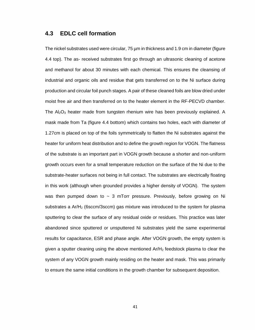
The nickel substrates used were circular, 75 µm in thickness and 1.9 cm in diameter (figure
4.4 top). The as- received substrates first go through an ultrasonic cleaning of acetone
and methanol for about 30 minutes with each chemical. This ensures the cleansing of
industrial and organic oils and residue that gets transferred on to the Ni surface during
production and circular foil punch stages. A pair of these cleaned foils are blow dried under
moist free air and then transferred on to the heater element in the RF-PECVD chamber.
The Al2O3 heater made from tungsten rhenium wire has been previously explained. A
mask made from Ta (figure 4.4 bottom) which contains two holes, each with diameter of
1.27cm is placed on top of the foils symmetrically to flatten the Ni substrates against the
heater for uniform heat distribution and to define the growth region for VOGN. The flatness
of the substrate is an important part in VOGN growth because a shorter and non-uniform
growth occurs even for a small temperature reduction on the surface of the Ni due to the
substrate-heater surfaces not being in full contact. The substrates are electrically floating
in this work (although when grounded provides a higher density of VOGN). The system
was then pumped down to ~ 3 mTorr pressure. Previously, before growing on Ni
substrates a Ar/H2 (6sccm/3sccm) gas mixture was introduced to the system for plasma
sputtering to clear the surface of any residual oxide or residues. This practice was later
abandoned since sputtered or unsputtered Ni substrates yield the same experimental
results for capacitance, ESR and phase angle. After VOGN growth, the empty system is
given a sputter cleaning using the above mentioned Ar/H2 feedstock plasma to clear the
system of any VOGN growth mainly residing on the heater and mask. This was primarily
to ensure the same initial conditions in the growth chamber for subsequent deposition.
42
Figure 4.4: (top) VOGN grown Ni electrode pair. (bottom) the heavy Ta mask used to
define the growth region and insure uniform heat distribution of Ni substrates.
After the samples have been placed on the heater, the system was pumped down to ~3
mTorr and the heater adjusted to a current chosen from the temperature calibration graph
(figure 4.5) to provide optimal VOGN growth.
The C2H2/H2 feedstock of 4:1 ratio was used during the VOGN growth. The normal growth
time was 10 minutes and the normal power of the RF power supply was 1000W. The total
pressure dropped from ~40 mTorr before the plasma is ignited, to ~10 mT during the
growth period. This indicates the growth chamber walls having a pumping effect for the
generated ions. After the growth was continued for the desired period, the plasma was
extinguished and the heater current gradually reduced to take the overall system to room
temperature.
43
The VOGN grown pair was then made into an EDLC by using the methods mentioned in
chapter 3.
Previously [40], CH4 feedstock was used as the plasma gas in the VOGN growth stage.
The research described in this dissertation used only C2H2 as the growth gas. When CH4
was used, the VOGN sheets showed much more disordered structure and noticeably
thinner sheets [40], [41] than when C2H2 was used. The growth rate for VOGN using
C2H2/H2 feedstock was more rapid due to the higher CHX concentration in the RF plasma.
The growth rate was about 2.5 X greater for acetylene feedstock compared with methane
feedstock.
An acetylene molecule has twice the carbon amount when compared with methane. This
increases the carbon percentage available for VOGN growth in the RF plasma. Also, the
available hydrogen for an acetylene plasma is less than for a methane plasma. For optimal
growth, the partial pressure of hydrogen in acetylene feedstock plasma was ~ 6mTorr,
compared to a partial pressure of ~60mTorr for methane feedstock plasma [33]. These
results indicate the best VOGN growth (more vertical and much faster growth rate) comes
from acetylene feedstock.
44
Figure 4.5: Temperature calibration graph for the Al2O3 heater
45
4.4 Characterization and performance of VOGN on Ni
One of the main variables for VOGN growth is substrate temperature. Figure 4.6 shows
Figure 4.6: Morphology of VOGN on Ni for different substrate temperature. Scale bar is 1
µm
the variation of VOGN on Ni with temperature. At low temperatures from 620ºC up to about
750ºC the sheets show a uniform and much open structure with a lower nanosheet
density. The individual nanosheet thickness has been observed to be about 5 to 6
graphene sheets or ~2 nm [33]. The growths for temperatures beyond 800ºC shows
nanosheets with considerable disorder, less vertical, curled-up structure and reduced
openness. They exhibit “cauliflower like “structure when compared with the low
temperature growth.
The EIS performance of typical capacitor cells as a function of growth temperature are
shown in figures 4.7 and 4.8.
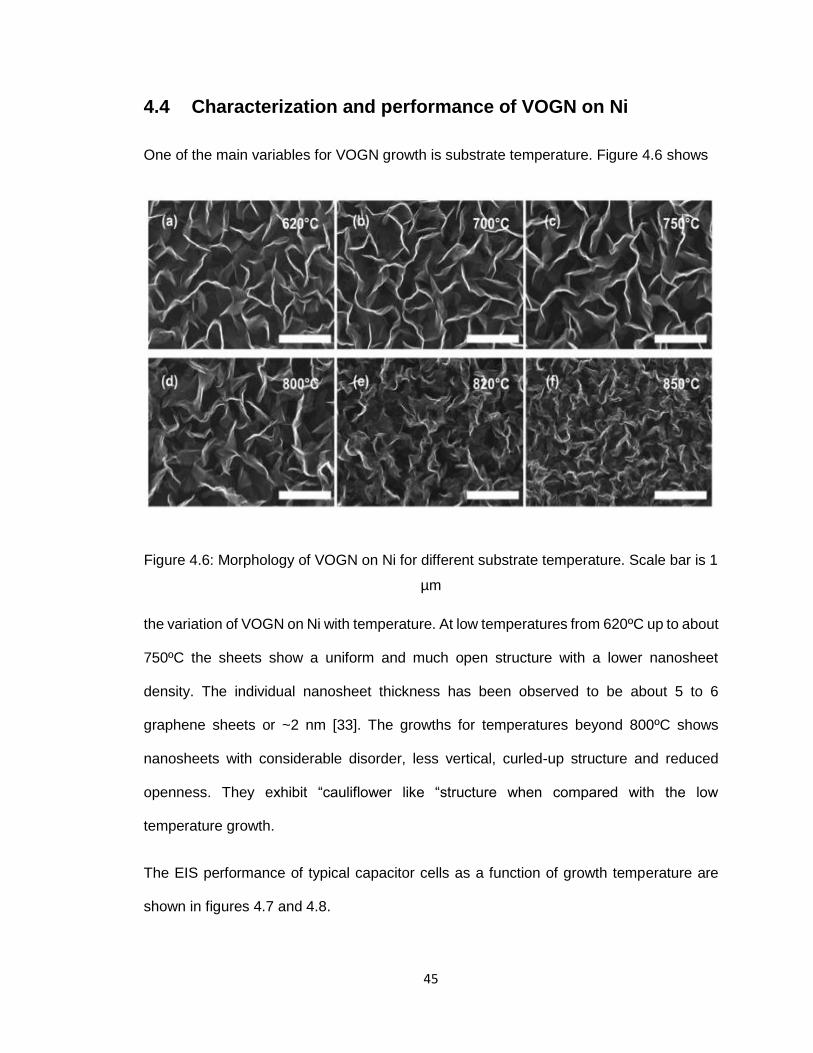
46
Figure 4.7: (a) Phase angle vs frequency graph (b) Complex plane plot for temperatures
from 620ºC-850ºC. The inset shows a vertical intersection with the X axis which shows
no porous electrode behavior and ESR levels between 0.07-0.08 Ω [33]
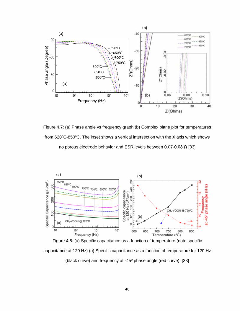
Figure 4.8: (a) Specific capacitance as a function of temperature (note specific
capacitance at 120 Hz) (b) Specific capacitance as a function of temperature for 120 Hz
(black curve) and frequency at -45º phase angle (red curve). [33]
(a)
(b)
(a) (b)
47
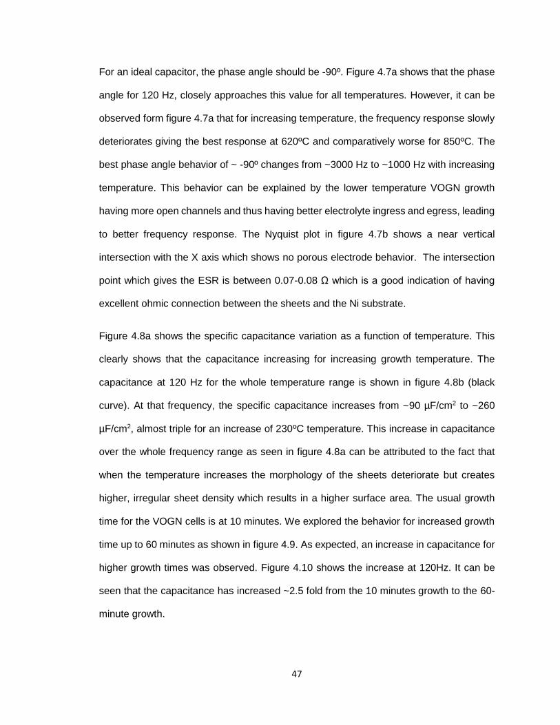
For an ideal capacitor, the phase angle should be -90º. Figure 4.7a shows that the phase
angle for 120 Hz, closely approaches this value for all temperatures. However, it can be
observed form figure 4.7a that for increasing temperature, the frequency response slowly
deteriorates giving the best response at 620ºC and comparatively worse for 850ºC. The
best phase angle behavior of ~ -90º changes from ~3000 Hz to ~1000 Hz with increasing
temperature. This behavior can be explained by the lower temperature VOGN growth
having more open channels and thus having better electrolyte ingress and egress, leading
to better frequency response. The Nyquist plot in figure 4.7b shows a near vertical
intersection with the X axis which shows no porous electrode behavior. The intersection
point which gives the ESR is between 0.07-0.08 Ω which is a good indication of having
excellent ohmic connection between the sheets and the Ni substrate.
Figure 4.8a shows the specific capacitance variation as a function of temperature. This
clearly shows that the capacitance increasing for increasing growth temperature. The
capacitance at 120 Hz for the whole temperature range is shown in figure 4.8b (black
curve). At that frequency, the specific capacitance increases from ~90 µF/cm2 to ~260
µF/cm2, almost triple for an increase of 230ºC temperature. This increase in capacitance
over the whole frequency range as seen in figure 4.8a can be attributed to the fact that
when the temperature increases the morphology of the sheets deteriorate but creates
higher, irregular sheet density which results in a higher surface area. The usual growth
time for the VOGN cells is at 10 minutes. We explored the behavior for increased growth
time up to 60 minutes as shown in figure 4.9. As expected, an increase in capacitance for
higher growth times was observed. Figure 4.10 shows the increase at 120Hz. It can be
seen that the capacitance has increased ~2.5 fold from the 10 minutes growth to the 60-
minute growth.
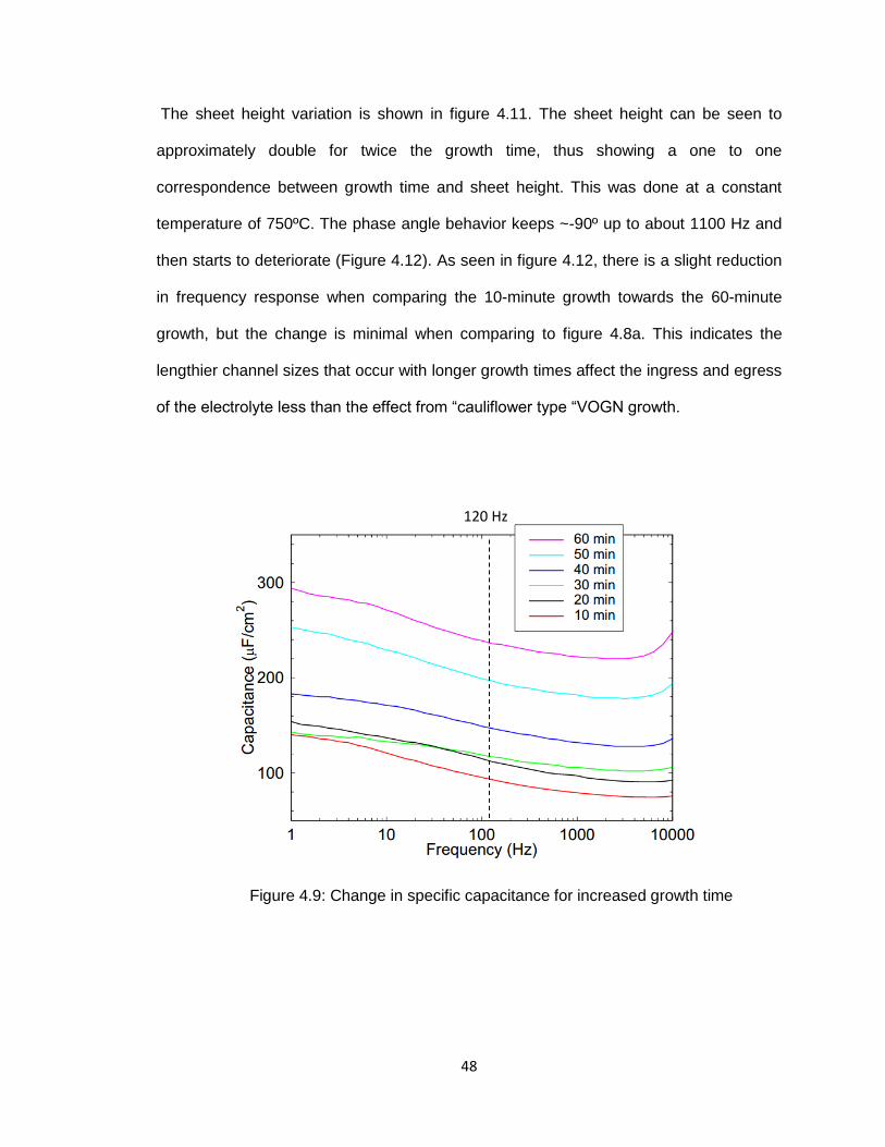
48
The sheet height variation is shown in figure 4.11. The sheet height can be seen to
approximately double for twice the growth time, thus showing a one to one
correspondence between growth time and sheet height. This was done at a constant
temperature of 750ºC. The phase angle behavior keeps ~-90º up to about 1100 Hz and
then starts to deteriorate (Figure 4.12). As seen in figure 4.12, there is a slight reduction
in frequency response when comparing the 10-minute growth towards the 60-minute
growth, but the change is minimal when comparing to figure 4.8a. This indicates the
lengthier channel sizes that occur with longer growth times affect the ingress and egress
of the electrolyte less than the effect from “cauliflower type “VOGN growth.
120 Hz
Figure 4.9: Change in specific capacitance for increased growth time
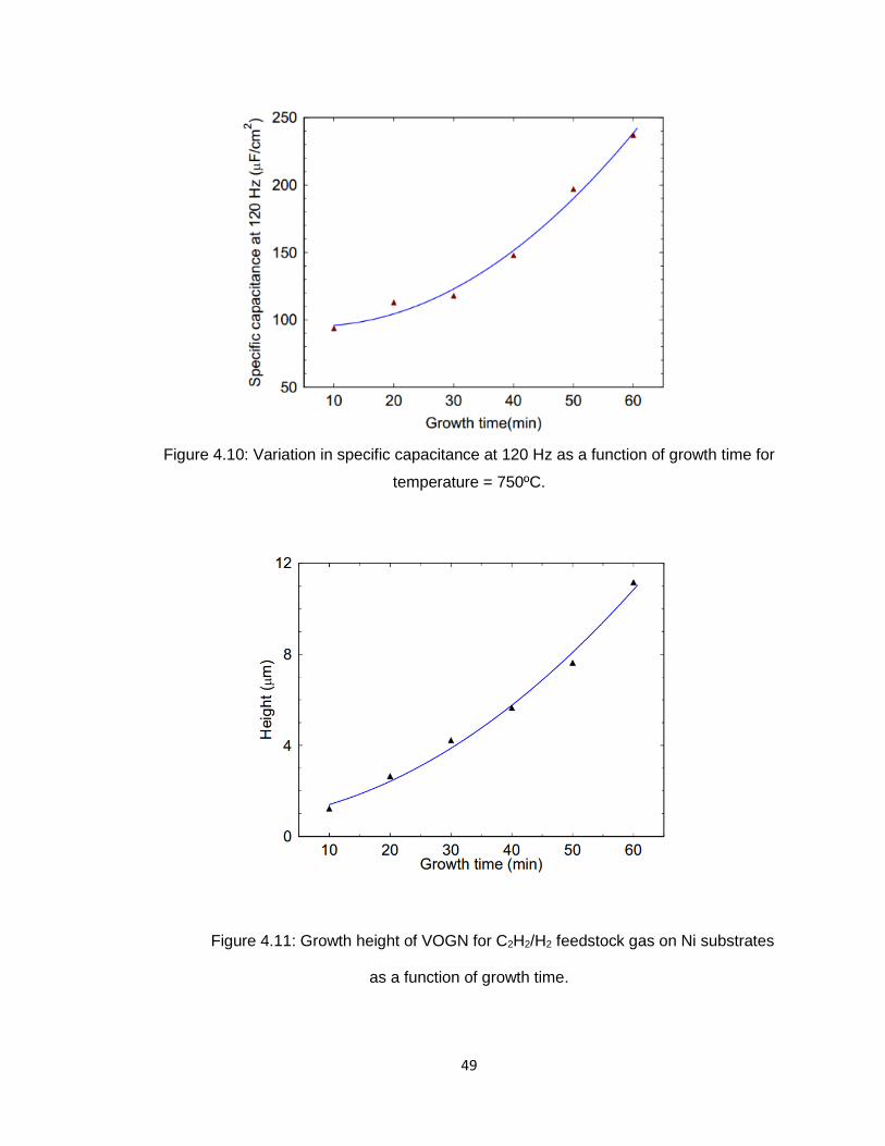
49
Figure 4.10: Variation in specific capacitance at 120 Hz as a function of growth time for
temperature = 750ºC.
Figure 4.11: Growth height of VOGN for C2H2/H2 feedstock gas on Ni substrates
as a function of growth time.
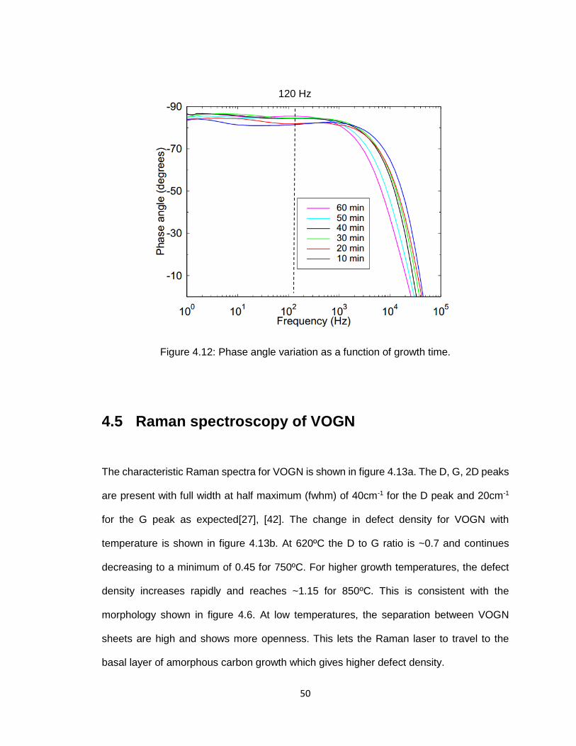
50
Figure 4.12: Phase angle variation as a function of growth time.
4.5 Raman spectroscopy of VOGN
The characteristic Raman spectra for VOGN is shown in figure 4.13a. The D, G, 2D peaks
are present with full width at half maximum (fwhm) of 40cm-1 for the D peak and 20cm-1
for the G peak as expected[27], [42]. The change in defect density for VOGN with
temperature is shown in figure 4.13b. At 620ºC the D to G ratio is ~0.7 and continues
decreasing to a minimum of 0.45 for 750ºC. For higher growth temperatures, the defect
density increases rapidly and reaches ~1.15 for 850ºC. This is consistent with the
morphology shown in figure 4.6. At low temperatures, the separation between VOGN
sheets are high and shows more openness. This lets the Raman laser to travel to the
basal layer of amorphous carbon growth which gives higher defect density.
120 Hz
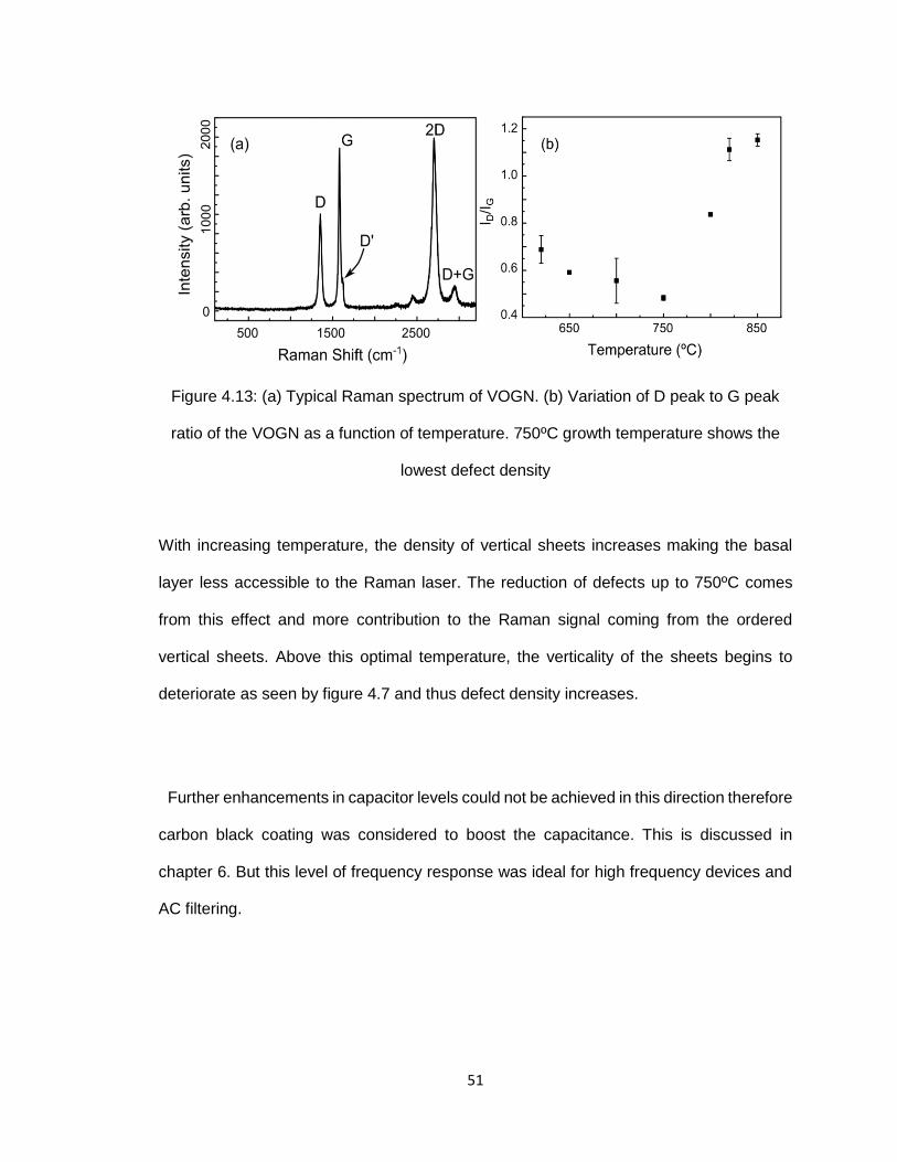
51
With increasing temperature, the density of vertical sheets increases making the basal
layer less accessible to the Raman laser. The reduction of defects up to 750ºC comes
from this effect and more contribution to the Raman signal coming from the ordered
vertical sheets. Above this optimal temperature, the verticality of the sheets begins to
deteriorate as seen by figure 4.7 and thus defect density increases.
Further enhancements in capacitor levels could not be achieved in this direction therefore
carbon black coating was considered to boost the capacitance. This is discussed in
chapter 6. But this level of frequency response was ideal for high frequency devices and
AC filtering.
Figure 4.13: (a) Typical Raman spectrum of VOGN. (b) Variation of D peak to G peak
ratio of the VOGN as a function of temperature. 750ºC growth temperature shows the
lowest defect density
52
Chapter 5. VOGN on Al
5.1 Introduction
Chapter 4 showed the development of EDLCs using VOGN on Ni substrates that shows
promising capacitive and response time results [33], [40], [43], [44] suitable for ac-line
filtering applications. The vertical nanosheets provide a very open morphology thus
providing good frequency response. The density and height of the nanosheets provide
the surface area necessary to give good specific capacitance. Although Ni (also Ta and
Nb) are excellent substrates for VOGN growth because of the high solubility of C (which
gives ohmic connection), they are heavy and expensive. Aluminum foil has been used for
many years for electrolytic capacitors and serves as a lighter and more affordable
substrate material for fast response, VOGN-electrode electric double layer capacitors.
Unfortunately, the low solubility of carbon in aluminum, which is about 1.3×10⁻² ppm by
weight at its melting point [45] and the thick stable native oxide (Al2O3) covering its surface,
hinders VOGN growth and ohmic contact. The native oxide causes capacitive rather than
ohmic coupling to the aluminum, which severely restricts the frequency response. Further,
the low melting point of Al (660°C), relative to Ni and Ta, makes it difficult to grow high
density nanosheets by RF-PECVD. Preliminary data indicates that the density of the
nanosheets is a function of the C2H2 inlet flow rate/partial pressure and the substrate
temperature [33].
5.2 Experimental
Aluminum substrates (99.99%), 0.076 mm thick and 1.9 cm in diameter, were
ultrasonically cleaned in acetone and then ethanol. A pair of the Al substrates was placed
on a planar resistance heater (rhenium-tungsten wire encapsulated in a parallel array of
53
Al2O3 tubes) and covered by a polished, two-hole tantalum mask (at floating potential),
within the RF-PECVD growth system. The mask was placed concentrically on top of the
substrates to define the 1.27 cm diameter graphene growth region and to ensure the
flatness of the sample for uniform heat distribution. The details of the RF-PECVD system
have been previously reported in chapter 3. After the system was evacuated to a pressure
~ 1 mTorr, the resistance heater was adjusted to approximately 150°C. Then, 6 sccm Ar
and 2 sccm H2 were admitted (with ±0.1 sccm accuracy) into the system for plasma
sputtering. Once a steady state pressure of ~100 mTorr was achieved, the RF plasma
(1100W power) was initiated. The combination of the resistive heating and heating from
the plasma raised the substrate temperature to ~620°C. The operational temperature of
the Al substrates was previously calibrated to ensure that no excursion above 660°C
occurred. The plasma sputtering was conducted for 10 minutes. The Ar and H2 supply for
sputtering were then valved off, while simultaneously inletting the C2H2 feedstock of 4-9
sccm into the system (p~12 mTorr) without extinguishing the plasma. The VOGN growth
was initiated and maintained for 10 minutes. Examination of the Al substrate oxide
variation as a function of temperature and the VOGN film purity were done by surface
diagnostics in ultra high vacuum (UHV). Auger data were taken using a PHI 590 system
with a double pass cylindrical mirror analyzer (GAR 15-255) operating at 2 kV energy and
an electron beam current of 500 nA. X-ray photoelectron spectroscopy data were
obtained from a PHI Quantera SXM instrument with an Al K alpha X-ray source (1486 eV).
The topography and the cross-sectional morphologies of the VOGN/Al thin films were
analyzed with Hitachi 4700 scanning electron spectroscopy system (SEM) operating at 10
kV.
Temperature desorption spectroscopy (TDS) of the uncoated Al substrate was conducted
using a SRS 200 mass spectrometer, with a Feulner cup (2 mm diameter aperture)
54
encapsulating the ion source. The mass spectrometer was linearly movable to within a
few mm of the Al surface. Raman spectra for analyzing the VOGN films was obtained by
Renishaw In-Via Raman spectroscope using the = 514 nm laser at 10 mW power.
The symmetric electric double layer capacitors were fabricated using two VOGN thin films
on Al substrates, separated by a 35-μm-thick cellulosic separator. The VOGN/Al foils and
separator were wetted with an organic electrolyte (1 M tetraethylammonium
tetrafluoroborate in propylene carbonate) before sealing the perimeter of the disks with a
thermoplastic using an impulse heat-seal apparatus. These sealed prototype capacitors
were 1.9 cm diameter by ∼175 μm thick and had a mass of less than 1 g. An Al lead was
resistance welded to the backside of each Al substrate to make electrical connection. Each
capacitor cell was then tested using electrochemical impedance spectroscopy (EIS). EIS
measurements were performed at 0.5 V bias. The capacitance was derived assuming a
series RC circuit model where C = -1//2fz” where f is the frequency and z” is the
corresponding imaginary part of the impedance.
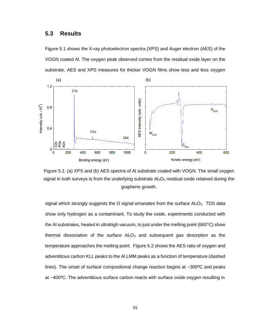
55
5.3 Results
Figure 5.1 shows the X-ray photoelectron spectra (XPS) and Auger electron (AES) of the
VOGN coated Al. The oxygen peak observed comes from the residual oxide layer on the
substrate. AES and XPS measures for thicker VOGN films show less and less oxygen
signal which strongly suggests the O signal emanates from the surface Al2O3. TDS data
show only hydrogen as a contaminant. To study the oxide, experiments conducted with
the Al substrates, heated in ultrahigh vacuum, to just under the melting point (660°C) show
thermal dissociation of the surface Al2O3 and subsequent gas desorption as the
temperature approaches the melting point. Figure 5.2 shows the AES ratio of oxygen and
adventitious carbon KLL peaks to the Al LMM peaks as a function of temperature (dashed
lines). The onset of surface compositional change reaction begins at ~300ºC and peaks
at ~400ºC. The adventitious surface carbon reacts with surface oxide oxygen resulting in
(a) (b)
Figure 5.1: (a) XPS and (b) AES spectra of Al substrate coated with VOGN. The small oxygen
signal in both surveys is from the underlying substrate Al2O3 residual oxide retained during the
graphene growth.
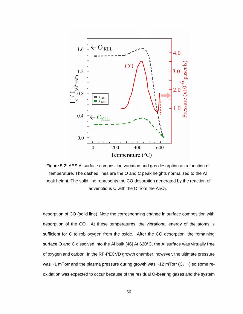
56
desorption of CO (solid line). Note the corresponding change in surface composition with
desorption of the CO. At these temperatures, the vibrational energy of the atoms is
sufficient for C to rob oxygen from the oxide. After the CO desorption, the remaining
surface O and C dissolved into the Al bulk [46] At 620°C, the Al surface was virtually free
of oxygen and carbon. In the RF-PECVD growth chamber, however, the ultimate pressure
was ~1 mTorr and the plasma pressure during growth was ~12 mTorr (C2H2) so some re-
oxidation was expected to occur because of the residual O-bearing gases and the system
Figure 5.2: AES Al surface composition variation and gas desorption as a function of
temperature. The dashed lines are the O and C peak heights normalized to the Al
peak height. The solid line represents the CO desorption generated by the reaction of
adventitious C with the O from the Al2O3.
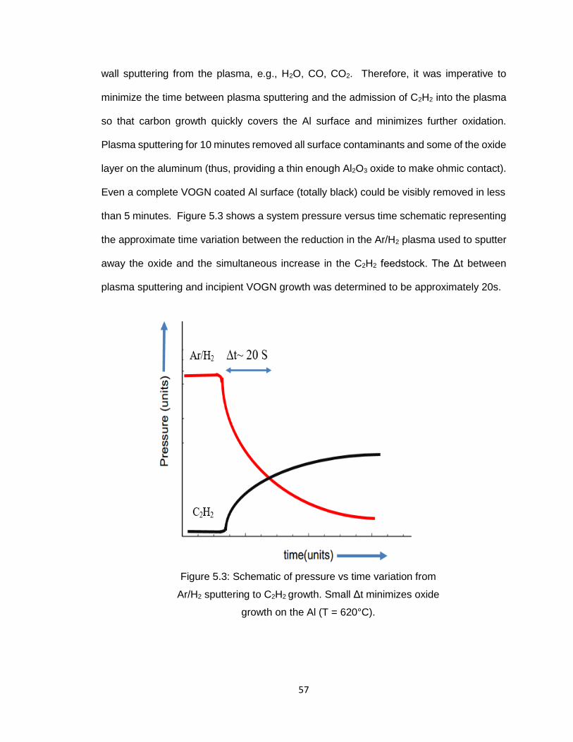
57
wall sputtering from the plasma, e.g., H2O, CO, CO2. Therefore, it was imperative to
minimize the time between plasma sputtering and the admission of C2H2 into the plasma
so that carbon growth quickly covers the Al surface and minimizes further oxidation.
Plasma sputtering for 10 minutes removed all surface contaminants and some of the oxide
layer on the aluminum (thus, providing a thin enough Al2O3 oxide to make ohmic contact).
Even a complete VOGN coated Al surface (totally black) could be visibly removed in less
than 5 minutes. Figure 5.3 shows a system pressure versus time schematic representing
the approximate time variation between the reduction in the Ar/H2 plasma used to sputter
away the oxide and the simultaneous increase in the C2H2 feedstock. The Δt between
plasma sputtering and incipient VOGN growth was determined to be approximately 20s.
Figure 5.3: Schematic of pressure vs time variation from
Ar/H2 sputtering to C2H2 growth. Small Δt minimizes oxide
growth on the Al (T = 620°C).
58
Figure 5.4 (top) shows the growth of the VOGN on the Al for a C2H2 admission rate of 7
sccm. The SEM is at a 45º angle. This shows perfect verticality of the VOGN sheets.
Figure 5.4 (bottom) shows the surface morphology in plain view of the VOGN on Al. The
inset shows the cross section of the film. The height of the film for a 10-minute growth is
~1.3 m. The films have an open, vertical and relatively uniform structure similar to that
previously observed with C2H2 and CH4 on Ni substrates (T ≤ 750°C) [33], [40]. The density
of the dominant sheets shown in figure 5.4 is uniform throughout the depth of VOGN film.
With higher magnification, one can see between the sheets that they go down to the
surface with uniform growth. At the substrate, there are a number of nuclei that have
much shorter growth because the taller VOGN preferentially robbed the carbon atoms and
ions in the plasma. The individual nanosheet thickness is, approximately, 2-3 nm (6-9
graphene layers), which is slightly thicker than the growth on Ni substrates using 75%
C2H2, 25% H2 feedstock [33].
Figure 5.5 shows the SEM topography of VOGN/Al for growths of 4 - 9 sccm of C2H2. Note
the increase in density of the sheets with flow rate. Using quantitative microscopy, the
density of sheet length increase is also plotted (Figure 5.6) and shows the increase with
flow rate. Quantitative microscopy is a material science statistical technique developed to
determine number of defects, grain boundaries, precipitates et cetera primarily from TEM
and SEM micrographs. The specific technique used here utilizes many test line segments
on the SEM images of the VOGN growth at different C2H2 flow rates, and calculating the
density of sheet length by the expression (π/2) *NL [47], where NL is the average number
of intersections of sheets with a random test line on the SEM micrograph. This is another
indication of the increase in the density of VOGN sheets as can be seen by visual
inspection of the SEM micrographs. It can be seen from figure 6 that the sheet density has
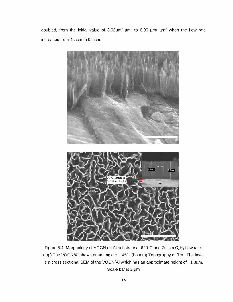
59
doubled, from the initial value of 3.02µm/ µm2 to 6.06 µm/ µm2 when the flow rate
increased from 4sccm to 9sccm.
Figure 5.4: Morphology of VOGN on Al substrate at 620ºC and 7sccm C2H2 flow rate.
(top) The VOGN/Al shown at an angle of ~45º. (bottom) Topography of film. The inset
is a cross sectional SEM of the VOGN/Al which has an approximate height of ~1.3µm.
Scale bar is 2 µm
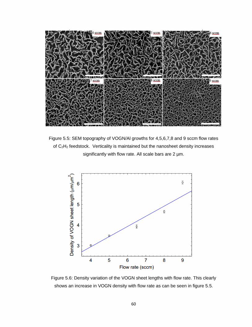
60
Figure 5.5: SEM topography of VOGN/Al growths for 4,5,6,7,8 and 9 sccm flow rates
of C2H2 feedstock. Verticality is maintained but the nanosheet density increases
significantly with flow rate. All scale bars are 2 µm.
Figure 5.6: Density variation of the VOGN sheet lengths with flow rate. This clearly
shows an increase in VOGN density with flow rate as can be seen in figure 5.5.
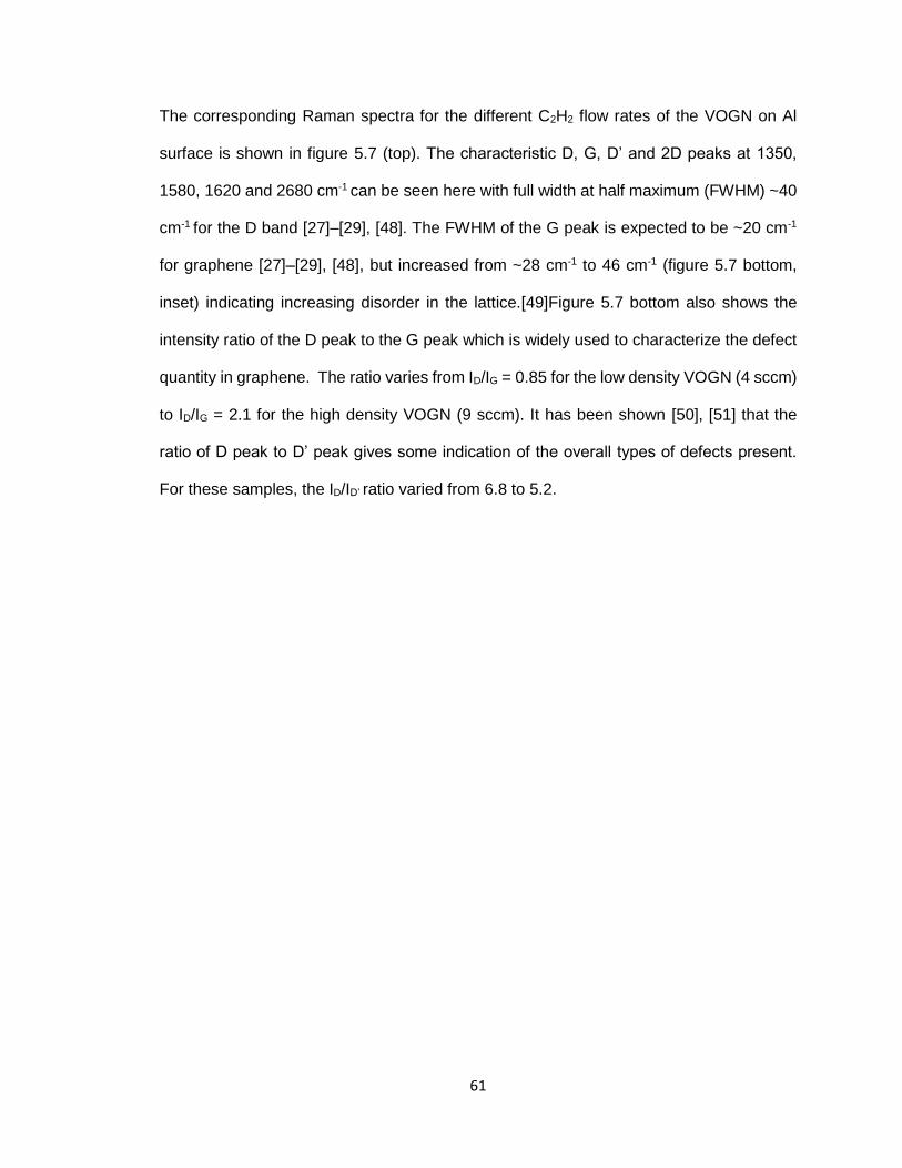
61
The corresponding Raman spectra for the different C2H2 flow rates of the VOGN on Al
surface is shown in figure 5.7 (top). The characteristic D, G, D’ and 2D peaks at 1350,
1580, 1620 and 2680 cm-1 can be seen here with full width at half maximum (FWHM) ~40
cm-1 for the D band [27]–[29], [48]. The FWHM of the G peak is expected to be ~20 cm-1
for graphene [27]–[29], [48], but increased from ~28 cm-1 to 46 cm-1 (figure 5.7 bottom,
inset) indicating increasing disorder in the lattice.[49]Figure 5.7 bottom also shows the
intensity ratio of the D peak to the G peak which is widely used to characterize the defect
quantity in graphene. The ratio varies from ID/IG = 0.85 for the low density VOGN (4 sccm)
to ID/IG = 2.1 for the high density VOGN (9 sccm). It has been shown [50], [51] that the
ratio of D peak to D’ peak gives some indication of the overall types of defects present.
For these samples, the ID/ID’ ratio varied from 6.8 to 5.2.
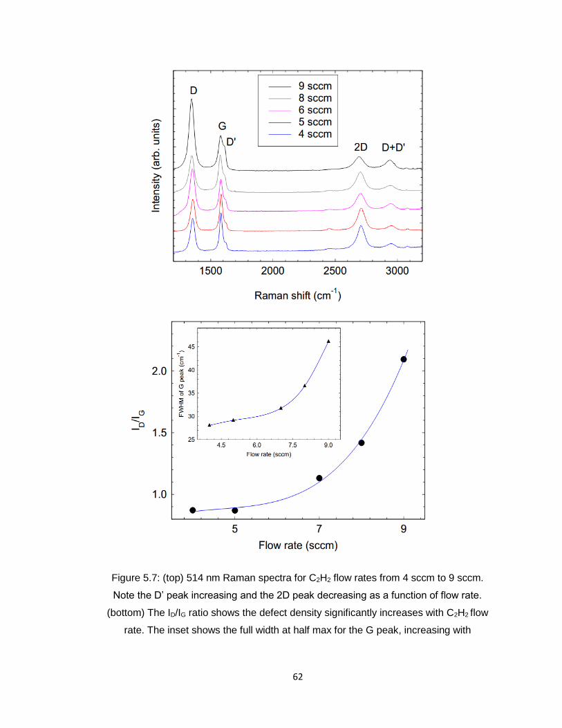
62
Figure 5.7: (top) 514 nm Raman spectra for C2H2 flow rates from 4 sccm to 9 sccm.
Note the D’ peak increasing and the 2D peak decreasing as a function of flow rate.
(bottom) The ID/IG ratio shows the defect density significantly increases with C2H2 flow
rate. The inset shows the full width at half max for the G peak, increasing with
disorder.
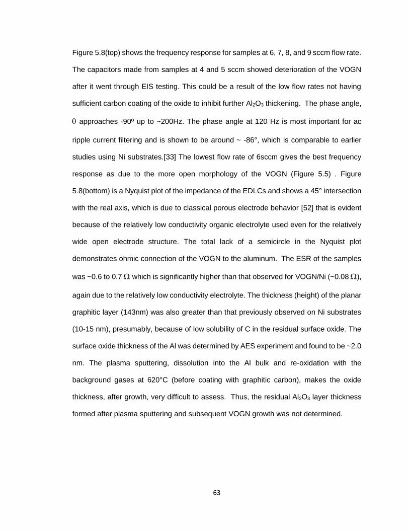
63
Figure 5.8(top) shows the frequency response for samples at 6, 7, 8, and 9 sccm flow rate.
The capacitors made from samples at 4 and 5 sccm showed deterioration of the VOGN
after it went through EIS testing. This could be a result of the low flow rates not having
sufficient carbon coating of the oxide to inhibit further Al2O3 thickening. The phase angle,
approaches -90º up to ~200Hz. The phase angle at 120 Hz is most important for ac
ripple current filtering and is shown to be around ~ -86°, which is comparable to earlier
studies using Ni substrates.[33] The lowest flow rate of 6sccm gives the best frequency
response as due to the more open morphology of the VOGN (Figure 5.5) . Figure
5.8(bottom) is a Nyquist plot of the impedance of the EDLCs and shows a 45° intersection
with the real axis, which is due to classical porous electrode behavior [52] that is evident
because of the relatively low conductivity organic electrolyte used even for the relatively
wide open electrode structure. The total lack of a semicircle in the Nyquist plot
demonstrates ohmic connection of the VOGN to the aluminum. The ESR of the samples
was ~0.6 to 0.7 which is significantly higher than that observed for VOGN/Ni (~0.08 ),
again due to the relatively low conductivity electrolyte. The thickness (height) of the planar
graphitic layer (143nm) was also greater than that previously observed on Ni substrates
(10-15 nm), presumably, because of low solubility of C in the residual surface oxide. The
surface oxide thickness of the Al was determined by AES experiment and found to be ~2.0
nm. The plasma sputtering, dissolution into the Al bulk and re-oxidation with the
background gases at 620°C (before coating with graphitic carbon), makes the oxide
thickness, after growth, very difficult to assess. Thus, the residual Al2O3 layer thickness
formed after plasma sputtering and subsequent VOGN growth was not determined.
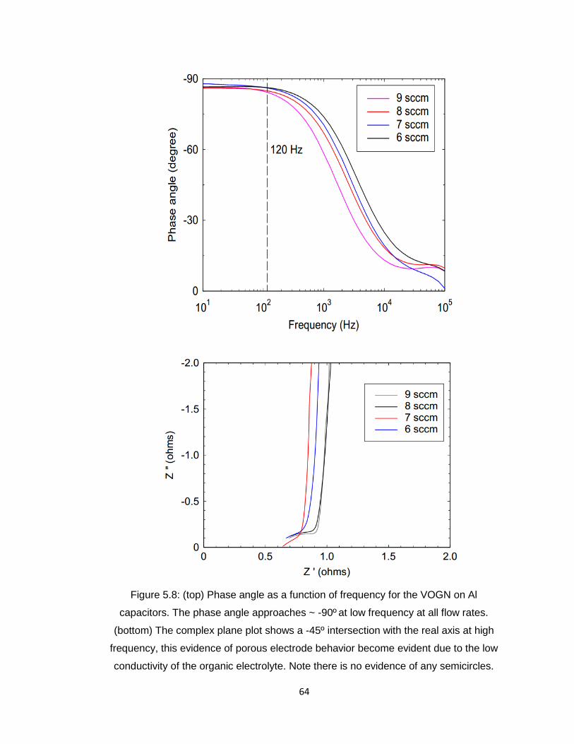
64
Figure 5.8: (top) Phase angle as a function of frequency for the VOGN on Al
capacitors. The phase angle approaches ~ -90º at low frequency at all flow rates.
(bottom) The complex plane plot shows a -45º intersection with the real axis at high
frequency, this evidence of porous electrode behavior become evident due to the low
conductivity of the organic electrolyte. Note there is no evidence of any semicircles.
65
Figure 5.9(top) shows the capacitance over the frequency range up to 105 Hz and
illustrates a stable capacitive behavior up to 104 Hz (capacitance at frequencies higher
than 105 Hz becomes divergent due to an artifact of the series-RC model). The highest
capacitance at 120 Hz was obtained at 9 sccm flow rate which was ~80 µF/cm2, which is
greater than the first studies using CH4 feedstock on Ni substrates [40]. This result is about
the same obtained using C2H2 feedstock on Ni at a temperature of 620ºC [33]. Figure
5.9(bottom) shows a plot of specific capacitance of the 10-minute growth films as a
function of flow rate for values at 120 Hz. The specific capacitance seems to double in
value when the flow rate increased from 6 sccm to 9 sccm, which indicates that the
increase in flow rate is not a one- to-one correspondence to the increase in capacitance.
The frequency at -45º is a common variable when assessing the performance of a
capacitor [53], [54]since at that phase angle, device reactance (Z”) and resistance (Z’) are
equal. In fig 5.9(b) it can be seen that this characteristic frequency varies from 4-1.5 kHz.
The ID/IG ratio shown in figure 5.7(bottom) suggests an increase in the defect density and
figure 5.9 shows an increase in specific capacitance. It is not yet clear what relative
contribution to the specific capacitance is made by increased surface area or increased
defects.
66
Figure 5.9: (top) The specific capacitance of the VOGN Al coin cells as a function of
frequency. The increasing flow rate of C2H2 gives an increasing capacitance (bottom)
The specific capacitance at 120 Hz (red curve) from top curve, shows increasing
capacitance with flow rate. The characteristic frequency at -45º phase angle (black
curve) also shows the decreasing behavior with increasing flow rate.
67
5.4 Discussion
The native Al2O3 oxide thickness on pure polycrystalline Al is 2.0 to 3.0 nm, depending on
the Al processing. We have previously measured the thickness of the foils used in this
work to be ~2.0 nm via AES. In the procedure to clean the foils before growth of the VOGN,
a ten-minute RF plasma sputter using 75% Ar and 25% H2 was employed. The technique
schematic shown in figure 5.3 was intended to minimize reoxidation after plasma
sputtering and this is verified by the measured ESR. However, even the shortest interval
between sputtering and growth (~20 seconds) was insufficient to prevent semicircular
formation in the complex plane plots at flow rates of 4 and 5 sccm of the C2H2. This was
further confirmed by the rather tenuous adherence of the coatings to the surface oxide, as
well. A minimum of 6 sccm of C2H2 was required to provide a carbon coating protective
layer that inhibits further oxidation. Presumably, this is because the density of ions and
neutrals in the plasma was sufficient to cover the existing Al2O3 before further oxidation.
The 45° slope in the complex plane plot shown in 5.8(b) is again due to porous electrode
behavior and primarily due to the resistance of the organic electrolyte (aqueous
electrolytes like KOH have much lower resistance and do not show this feature).
The relatively high defect ratio given by the Raman D band to G band ratio (compared to
that on Ni substrates) can be attributed to the chemically bonded H to the carbon atoms
and point defects incorporated in the higher dense growth of vertical sheets which also
significantly increases the number of defects arising from edge states. Edges (armchair
and zigzag) are considered as defects since they break the translational symmetry of the
overall graphene lattice. Armchair edges can give rise to the D peak due to the activation
of breathing mode [55]–[58] of 6 carbon atom ring in graphene. A D peak cannot be
created by a perfect zigzag edge [59]–[61] since it cannot initiate the process of inter-
valley scattering [29]. The D’ peak can be also seen due to the effects from both armchair
68
and zigzag edges. This peak is activated by the double resonance occurring as an intra-
valley process [29]. The previously discussed ID/ID’ ratio shows that the dominant defects
come from a combination of vacancy- like and boundary- like defects in which the ratio
indicates more defects arise from vacancies [49], [50].
The growth of VOGN has been explained in chapter 4 which describes Volmer-Weber
growth of carbon islands impinging on each other creating the vertical sheets. Previous
studies [34]–[37], [39] have reported radicals such as C4H2+, C4H3
+, C2H2+, C2H+ and
neutrals as the main growth constituents from the acetylene/hydrogen plasma, that
contributes to VOGN growth.
Although the sheet height is less than for VOGN on Ni (~2.25 µm T=750ºC) [3] due to the
low temperature, the increased density of the VOGN growth provides a roughly linear
increase in capacitance due to the increase in surface area and defects, which gives the
same type of value for the capacitance for VOGN on Ni and on Al. But as determined in
the VOGN/Ni work, there is a corresponding decrease in the frequency response.
However, even at the highest flow rate of C2H2 tested (9 sccm), a phase angle near -90°
was measured at 120 Hz. This suggests that these films are suitable for AC filtering. The
height of the nanosheets studied is only 1.3 µm, thus suggesting a substantial increase in
capacitance can be achieved by longer growth times beyond 10 minutes. Previous studies
of VOGN/Ni show a surface area increase C ~ A/2 behavior so a capacitance of 500
µF/cm2 can be achieved for a nanosheet height of 10µm. Since this is the first work to
achieve successful growth of VOGN on an Al substrate, specific capacitance has not yet
been optimized, but represents the first successful ohmic contact to Al achieved in this
process. We have observed a significant increase (>2x) in the VOGN density on the Al
by increasing the C2H2 flow rate. The increase in height of the sheets to 10 µm or greater
should provide a substantial increase in nanosheet surface area and, therefore,
69
capacitance. Finally, we have previously found that coating the graphene nanosheet
surface with carbon black provides a substantial capacitance increase. Optimization
experiments are presently underway.
The growth was achieved at an Al substrate temperature of 620°C, a C2H2 pressure of 12
mTorr and a plasma power of 1100W. Although Al has a low solubility of carbon and a
very stable native Al2O3 oxide, the growth method employed produced EDLC electrodes
with ohmic connection between the aluminum and the graphene and a capacitance
comparable to that of VOGN growth on similar height foils. The average specific
capacitance was found to be, approximately, 80 µF/cm2 (at 120Hz) with a VOGN
nanosheet height of ~1.3 µm. The ESR value for capacitors fabricated with VOGN/Al was
0.6-0.7 ohms which is higher than that measured for VOGN/Ni capacitors. The 45º angle
in the Nyquist plot comes directly as a result of using low-conductivity organic electrolyte
(PC) rather than a high-conductivity aqueous electrolyte (KOH). Future work includes in-
depth characterization of the VOGN growth on Al with a study of the growth parameters
to obtain optimal capacitor performance.
VOGN
70
Chapter 6. Carbon black coating on VOGN
6.1 Introduction.
The first conception of using vertically oriented graphene nanosheets (VOGN) thin films
as an electrical double layer capacitor (EDLC) was reported by Xin et.al. in 2009[62]. The
first experimental results of this concept were reported by Miller et.al. in 2010[43], [63]. In
the initial work, thin film VOGN deposited by radio frequency plasma enhanced chemical
vapor deposition (RF-PECVD) on Ni substrates foils using CH4/H2 feed stock provided
electrodes with excellent frequency response. The Ni substrates were selected because
of high carbon solubility and the tenuous NiO (native oxide) with temperature[32]. At the
growth temperature of ~750ºC, the surface oxide dissolved into the bulk, providing a good
C/Ni ohmic bond with low contact resistance. The VOGN films previously grown from
CH4/H2 feedstock for 20 minutes at a linear growth rate of ~70 nm/min resulted in
nanosheets that were less than 1 nm thick, less than 1 µm high and a spacing of 200 -
400 nm. The overall orientation of the sheets was predominantly vertical, but with irregular
shapes (potato chip like) because of the intrinsic stress from defects. However, the open
structure between the nanosheets provided excellent conditions for minimizing porous
electrode behavior, thus allowing good frequency response. These growth conditions
resulted in the first EDLCs having an RC time constant of less than 200 µs at 120 Hz[43].
However, for nanosheet heights less than one micrometer, only a specific capacitance of
~57 µF/cm2 was achieved. The ratio of Raman D band to G band showed a continual
decrease with growth time indicating that the defect density was decreasing with
increasing nanosheet height[40]. This performance suggested a potential thin film
capacitor suitable for AC filtering. Subsequent experimental development with C2H2/H2 as
feedstock, provided films with an increased growth rate to 190 nm/min and much improved
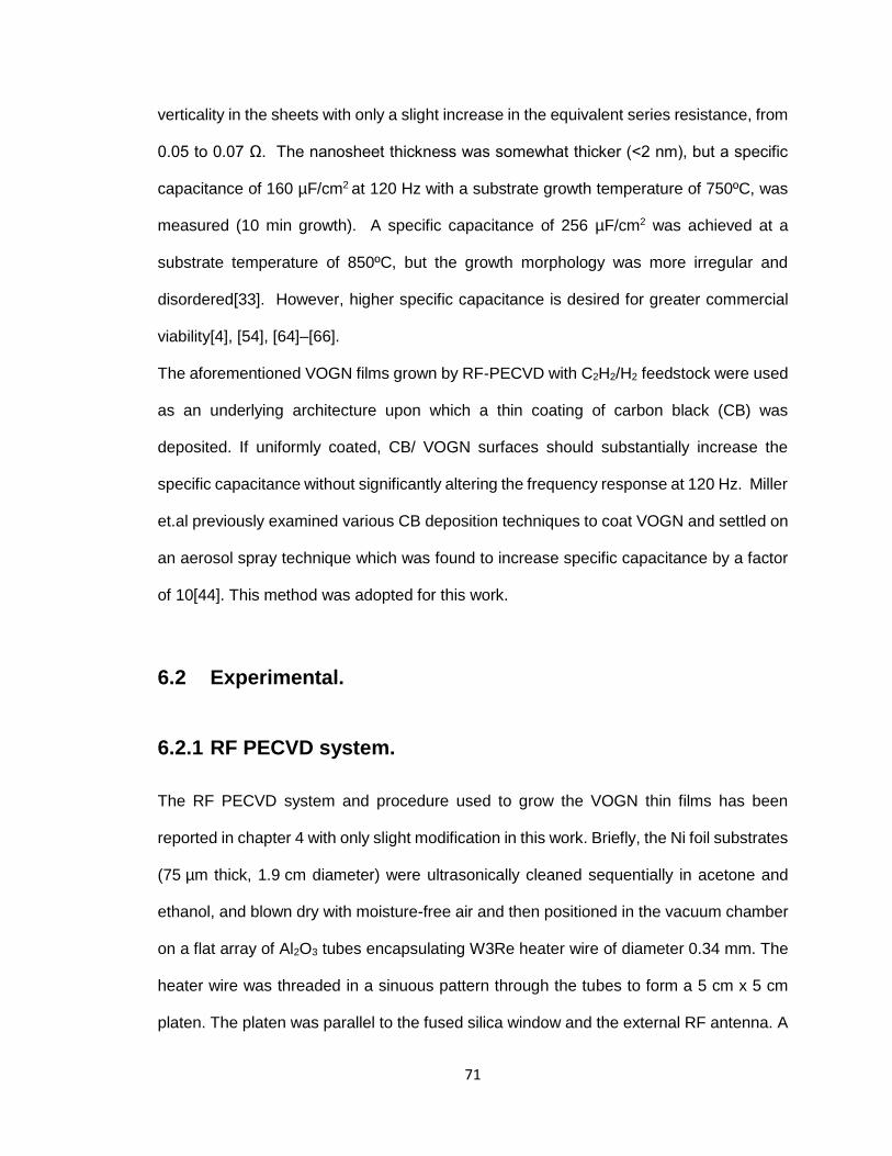
71
verticality in the sheets with only a slight increase in the equivalent series resistance, from
0.05 to 0.07 Ω. The nanosheet thickness was somewhat thicker (<2 nm), but a specific
capacitance of 160 µF/cm2 at 120 Hz with a substrate growth temperature of 750ºC, was
measured (10 min growth). A specific capacitance of 256 µF/cm2 was achieved at a
substrate temperature of 850ºC, but the growth morphology was more irregular and
disordered[33]. However, higher specific capacitance is desired for greater commercial
viability[4], [54], [64]–[66].
The aforementioned VOGN films grown by RF-PECVD with C2H2/H2 feedstock were used
as an underlying architecture upon which a thin coating of carbon black (CB) was
deposited. If uniformly coated, CB/ VOGN surfaces should substantially increase the
specific capacitance without significantly altering the frequency response at 120 Hz. Miller
et.al previously examined various CB deposition techniques to coat VOGN and settled on
an aerosol spray technique which was found to increase specific capacitance by a factor
of 10[44]. This method was adopted for this work.
6.2 Experimental.
6.2.1 RF PECVD system.
The RF PECVD system and procedure used to grow the VOGN thin films has been
reported in chapter 4 with only slight modification in this work. Briefly, the Ni foil substrates
(75 µm thick, 1.9 cm diameter) were ultrasonically cleaned sequentially in acetone and
ethanol, and blown dry with moisture-free air and then positioned in the vacuum chamber
on a flat array of Al2O3 tubes encapsulating W3Re heater wire of diameter 0.34 mm. The
heater wire was threaded in a sinuous pattern through the tubes to form a 5 cm x 5 cm
platen. The platen was parallel to the fused silica window and the external RF antenna. A
72
two-hole, polished tantalum mask was placed on top of the substrates to define the
graphene growth region (1.27 cm diameter) for a pair of circular electrodes. The growth
sequence begins by evacuating the system to a pressure <2 mTorr. The Ni substrates
were heated in 10 mTorr H2 to the desired growth temperature (750ºC in this case).
Nanosheet growths were conducted using 80% C2H2 and 20% H2 at a total pressure of
~20 mTorr and 1000 W plasma power for 10 and 20 minute VOGN growth times. The Ta
mask and the substrates were unbiased and allowed to electrically float to near the plasma
potential (~22V) determined by a Langmuir probe. Following each deposition, the growth
chamber was cleaned by plasma-etching in a 60-40 Ar/H2 mixture for ~5 minutes to
remove surface contamination and until the white of the alumina ribs of the platen were
observed.
6.2.2 Diagnostic systems.
For surface analysis, the Ni substrates were initially degreased in an ultrasonic cleaner,
sequentially with acetone for 10 minutes followed by 10 minutes in ethyl alcohol, and then
dried using ultrahigh purity nitrogen. The surfaces of the substrates before and after
coating were examined by Auger electron spectroscopy (AES, Physical Electronics 590
system with a 15-255 GAR double pass cylindrical mirror analyzer operated at 2 kV beam
energy and 0.5 µA beam current). The substrates were admitted to the system introduction
chamber (p < 1x10⁻⁹ Torr) and radiatively heated to 250ºC for 30 minutes to degas
adsorbed water on the sample and sample holder before transfer into the analysis
chamber (p < 1x10-11 Torr) for surface study. The uncoated Ni foil was pristine showing no
contaminants (<1%) with the exception of the residual oxygen from the native oxide and
the adventitious carbon in the oxide. Samples were RF-PECVD coated using the C2H2/H2
73
feedstock for 10 - 60 minutes at 10 minute intervals. The surface morphology of the VOGN
was examined using scanning electron microscopy (SEM, Hitachi S-4700, operated at
15 kV). The structure and defect information of the graphene films were studied by a
Renishaw in-via Raman spectroscope using a 514 nm wavelength laser.
6.2.3 Coating method.
The carbon black used was Cabot SC3 (CB). As shown in Figure 6.1(a), the carbon black
is comprised of clusters of ~10 nm diameter particles[67], [68]. Colloidal suspension
preparation involved mechanical crushing the CB to eliminate large agglomerates followed
by high-power ultrasonic treatment in a liquid for 4h to minimize cluster size. Several
alcohols and n-methyl pyrrolidone (NMP), were tried sometimes together, but always
without binders or surfactants. Important factors included suspension stability against
settling, the ability to wet the VOGN surfaces, and the drying rate after dispensing. Figure
6.1(b) shows the glass container with the CB colloidal suspension. The container in 6.1(b)
was pressurized and manually swept over the VOGN surface (synchronized with a
Figure 6.1: (a) Spherical carbon particles of ~10 nm size in various cluster sizes. (b)
Carbon black suspension container, pressurized, pendulum synchronized aerosol spray
(c) Coated VOGN/Ni electrodes.
b
c a
74
pendulum) to coat the VOGN/Ni samples in ~1s spray intervals. The distance between the
spray nozzle and the VOGN surface was ~10 cm. Figure 6.1(c) shows the coated
VOGN/Ni electrodes. Other deposition methods, such as dip coating, liquid drop coating,
ink jet coating and electrospray coating were tried, but the aerosol spray coating provided
the best results[44].
6.2.4 VOGN architecture.
Figure 6.2 shows the VOGN/Ni morphology (plan view) without CB coating grown at 750ºC
and 1000W RF power with C2H2/H2 feedstock for 10 minutes. A growth temperature of
750ºC was selected for the uncoated VOGN based on previous work that showed the best
open morphology and the lowest defect density. Figure 6.2 inset is the cross section of
the VOGN film without coating. The film height for these conditions is ~1.2 microns. This
cross section was obtained by growing on a Ni 1000 nm film produced by magnetron
sputtering on a Si (100) wafer. This allowed a clean break by cleaving so that a good
measure of the carbon base layer and the nanosheet height could be obtained[33]. Figure
6.2 represents the underlying architecture for the carbon black coating employed in this
work. The highest specific capacitance for this uncoated material, for a 10 min growth, at
750ºC growth temperature, is ~160 µF/cm2 at 120 Hz[33].
The Figure 4.11 shown in chapter 4 shows the behavior of nanosheet height as a function
of time. This shows a monotonically increasing quadratic behavior for VOGN height with
growth time. The average growth rate of ~195 nm/min was found to be consistent with
that found in previous work[33], The nanosheet height actually increases faster than the
specific capacitance similar to what was observed for VOGN grown from CH4/H2
feedstock[40].
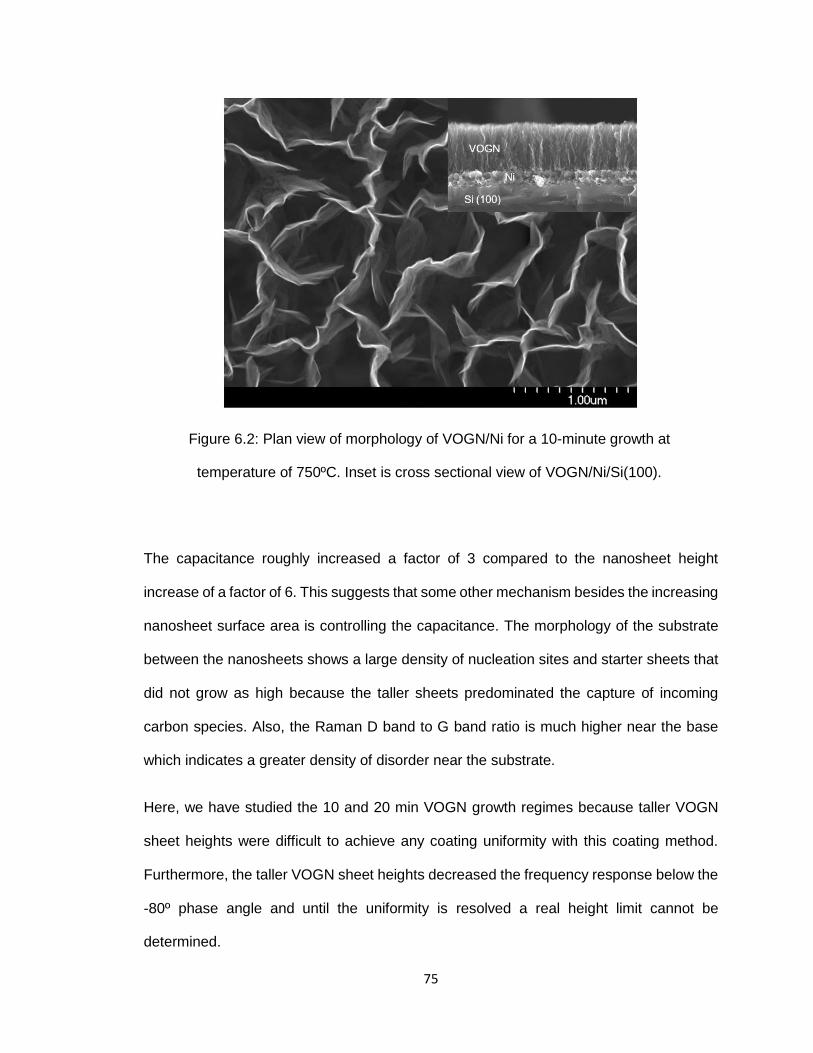
75
The capacitance roughly increased a factor of 3 compared to the nanosheet height
increase of a factor of 6. This suggests that some other mechanism besides the increasing
nanosheet surface area is controlling the capacitance. The morphology of the substrate
between the nanosheets shows a large density of nucleation sites and starter sheets that
did not grow as high because the taller sheets predominated the capture of incoming
carbon species. Also, the Raman D band to G band ratio is much higher near the base
which indicates a greater density of disorder near the substrate.
Here, we have studied the 10 and 20 min VOGN growth regimes because taller VOGN
sheet heights were difficult to achieve any coating uniformity with this coating method.
Furthermore, the taller VOGN sheet heights decreased the frequency response below the
-80º phase angle and until the uniformity is resolved a real height limit cannot be
determined.
Figure 6.2: Plan view of morphology of VOGN/Ni for a 10-minute growth at
temperature of 750ºC. Inset is cross sectional view of VOGN/Ni/Si(100).
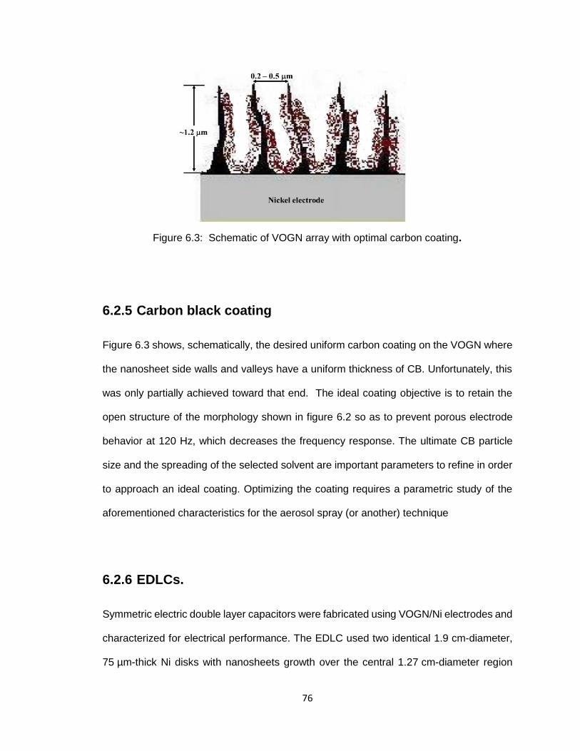
76
6.2.5 Carbon black coating
Figure 6.3 shows, schematically, the desired uniform carbon coating on the VOGN where
the nanosheet side walls and valleys have a uniform thickness of CB. Unfortunately, this
was only partially achieved toward that end. The ideal coating objective is to retain the
open structure of the morphology shown in figure 6.2 so as to prevent porous electrode
behavior at 120 Hz, which decreases the frequency response. The ultimate CB particle
size and the spreading of the selected solvent are important parameters to refine in order
to approach an ideal coating. Optimizing the coating requires a parametric study of the
aforementioned characteristics for the aerosol spray (or another) technique
6.2.6 EDLCs.
Symmetric electric double layer capacitors were fabricated using VOGN/Ni electrodes and
characterized for electrical performance. The EDLC used two identical 1.9 cm-diameter,
75 µm-thick Ni disks with nanosheets growth over the central 1.27 cm-diameter region
Figure 6.3: Schematic of VOGN array with optimal carbon coating.
77
(1.26 cm2). See Figure 6.1(c). The two disks were separated by a 25-µm-thick
microporous separator. The VOGN and separator were wetted with an aqueous electrolyte
(25 wt% potassium hydroxide) before sealing the perimeter of the disks with a
thermoplastic using an impulse heat-seal apparatus. These packaged prototypes were
1.9 cm diameter by ~175 µm thick and had a mass of less than 1 g. The height of the
VOGN on each electrode was about 1.5 µm, which is negligible compared with device
dimensions. A nickel lead was spot-welded to the backside of each Ni substrate to make
electrical connection. This EDLC design circumvents the passive-layer problem often
encountered with the usual button/coin cell designs
6.3 Results
6.3.1 Topography
Figure 6.4 shows an array of SEMs at the same magnification aerosol spray CB coated
from 1s to 6s. Eight s coatings were almost totally crusted over. Note that a very small
amount of coating has penetrated down into the valleys of the VOGN, but the CB thickness
toward the base was not determined. The overall thickness observed at the upper regions
of the array appears to be around 50 nm or more. As shown in the 5 µm scale bar
micrograph, even 1 s coating time, some crusting can be observed. Some small clumps
were also observed, probably from a lack of complete sonication. Longer coating times
resulted in greater crusting where the lateral crusting growth actually began to seal off the
lower regions of the film, thus preventing any further coating of the base and valley
between the sheets. However, even with this situation, there was still sufficient electrolyte
wetting of the underlying surface to achieved acceptable 120 Hz response along with a

78
significant increase in the specific capacitance. A 6-s coating resulted in a specific
capacitance >1 mF/cm2 at 120 Hz for an underlying 10 minute VOGN/Ni growth.
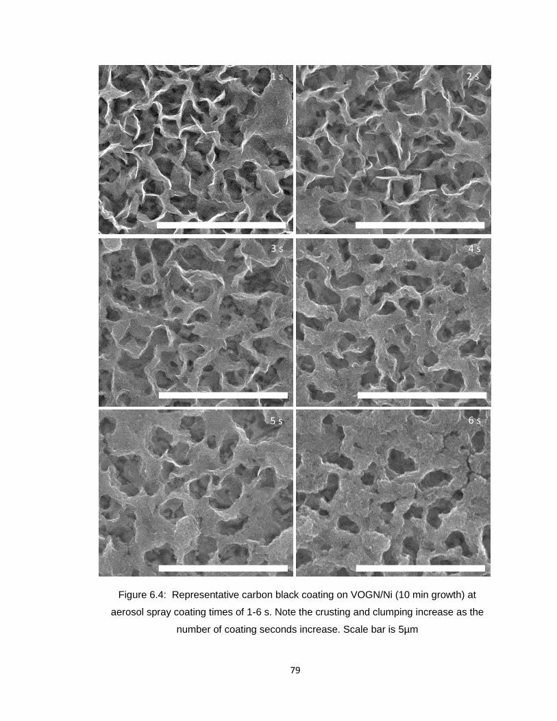
79
1 s 2 s
3 s 4 s
5 s 6 s
Figure 6.4: Representative carbon black coating on VOGN/Ni (10 min growth) at
aerosol spray coating times of 1-6 s. Note the crusting and clumping increase as the
number of coating seconds increase. Scale bar is 5µm
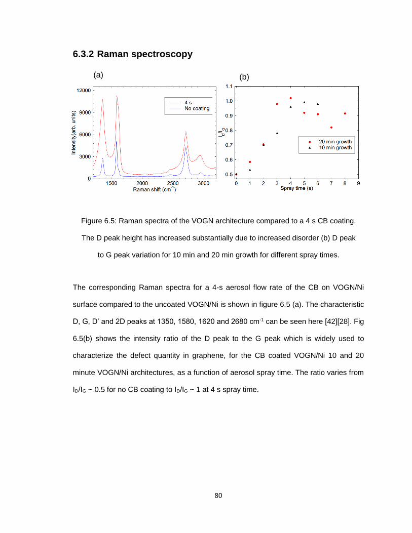
80
6.3.2 Raman spectroscopy
The corresponding Raman spectra for a 4-s aerosol flow rate of the CB on VOGN/Ni
surface compared to the uncoated VOGN/Ni is shown in figure 6.5 (a). The characteristic
D, G, D’ and 2D peaks at 1350, 1580, 1620 and 2680 cm-1 can be seen here [42][28]. Fig
6.5(b) shows the intensity ratio of the D peak to the G peak which is widely used to
characterize the defect quantity in graphene, for the CB coated VOGN/Ni 10 and 20
minute VOGN/Ni architectures, as a function of aerosol spray time. The ratio varies from
ID/IG ~ 0.5 for no CB coating to ID/IG ~ 1 at 4 s spray time.
(b)
(a)
Figure 6.5: Raman spectra of the VOGN architecture compared to a 4 s CB coating.
The D peak height has increased substantially due to increased disorder (b) D peak
to G peak variation for 10 min and 20 min growth for different spray times.
81
6.3.3 Electrochemical impedance spectroscopy
Electrochemical impedance spectroscopy (EIS) measurements were performed at 0.5 V
bias on symmetric capacitors after electrodes were completely wetted by the electrolyte.
The AC capacitance was derived, assuming a series-RC circuit model, from 𝐶 =−1
2𝜋𝑓𝑍",
where f is frequency in Hz and Z” is the corresponding imaginary part of the impedance.
The areal specific capacitance was calculated by 𝐶𝑠 = 𝐶 𝐴⁄ , where C is the AC
capacitance of the device and A is the geometric area of the film growth region. All values
reported are for two-terminal capacitors, not single electrodes. The complex plane and
phase angle plots for all CB deposition times of 10-minute (a) and 20-minute (b) VOGN
growths are presented in figure 6.6. Note the verticality of the Nyquist curves for the 10
min and 20-minute VOGN/Ni growths for all CB coating times. They show no distributed
charge storage behavior, thus indicating that even the longest deposition time of 8 s
(virtually crusted over) provides an EDLC capacitor suitable for high-frequency operation.
Although the coatings shown in figure 5 for a 6-s coating time, are significantly crusted
relative to the nanosheet thickness (~2 nm) the path length for ions within the coating is
short enough and the electrolyte conductivity high enough so that no porous electrode
behavior is observed. ESR values range from 0.05 to 0.07 Ω, similar to that measured for
uncoated VOGN/Ni with C2H2/H2 feedstock[33]. These values represent good ohmic
contact between the CB/VOGN and the Ni substrate and show no resistance increase
from the thick carbon black coatings. The phase angle plots of all the CB coated VOGN/Ni
EDLCs have a phase angle of -80º to -85º although the 8-s coating for the 20 minute
VOGN/Ni growth was on the edge of ideal capacitor behavior. The frequency at -45º, to
which most comparisons are made, was ~2 kHz for 10 min growth, 6s coating and ~1 kHz
for 20 min growth 8s coating. As expected, the frequency response worsened with
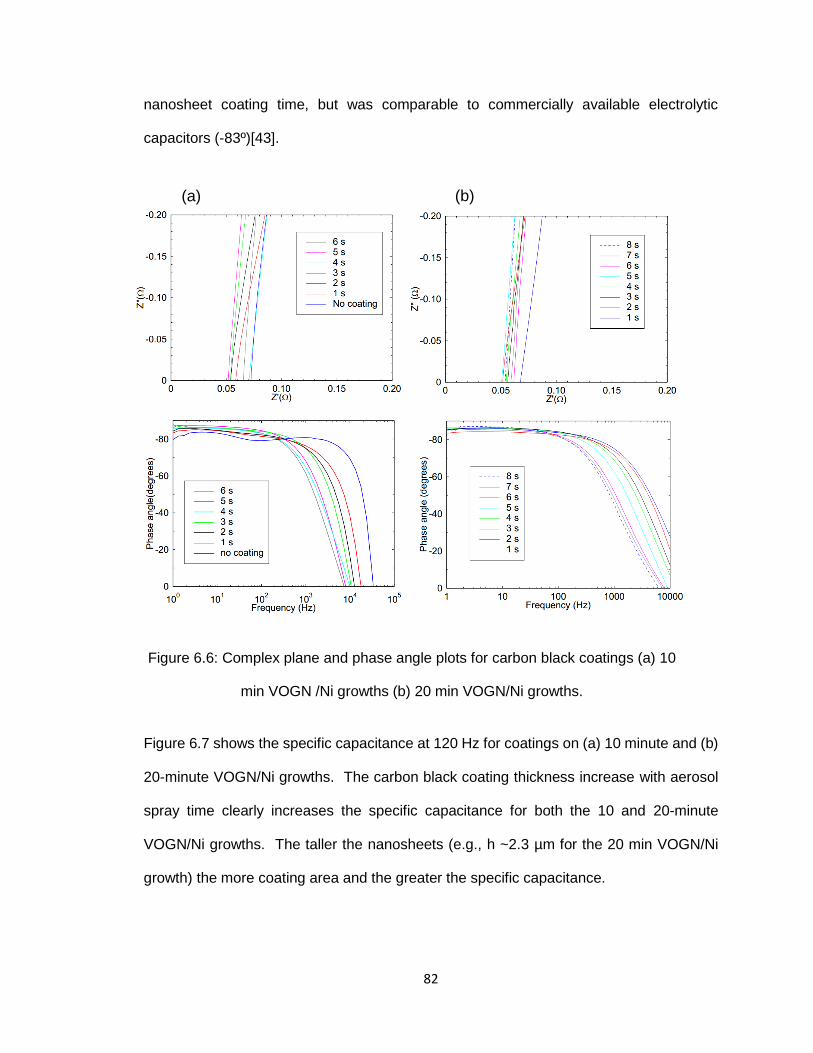
82
nanosheet coating time, but was comparable to commercially available electrolytic
capacitors (-83º)[43].
Figure 6.7 shows the specific capacitance at 120 Hz for coatings on (a) 10 minute and (b)
20-minute VOGN/Ni growths. The carbon black coating thickness increase with aerosol
spray time clearly increases the specific capacitance for both the 10 and 20-minute
VOGN/Ni growths. The taller the nanosheets (e.g., h ~2.3 µm for the 20 min VOGN/Ni
growth) the more coating area and the greater the specific capacitance.
Figure 6.6: Complex plane and phase angle plots for carbon black coatings (a) 10
min VOGN /Ni growths (b) 20 min VOGN/Ni growths.
(b) (a)
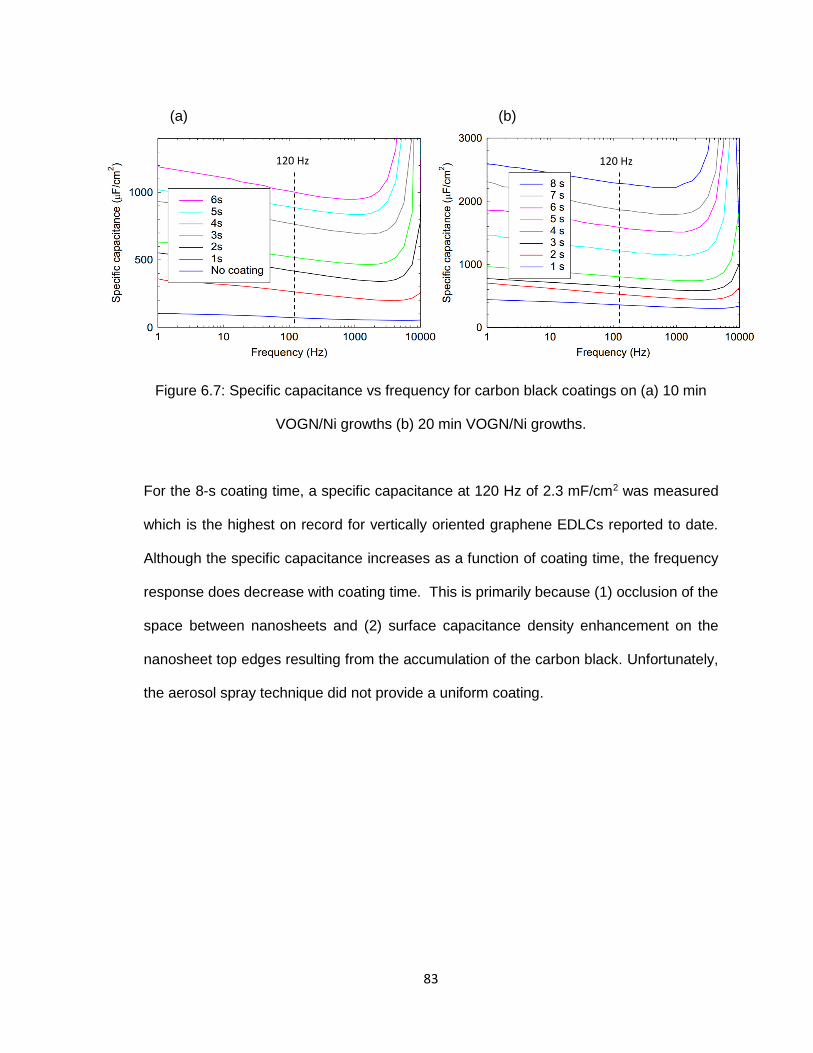
83
For the 8-s coating time, a specific capacitance at 120 Hz of 2.3 mF/cm2 was measured
which is the highest on record for vertically oriented graphene EDLCs reported to date.
Although the specific capacitance increases as a function of coating time, the frequency
response does decrease with coating time. This is primarily because (1) occlusion of the
space between nanosheets and (2) surface capacitance density enhancement on the
nanosheet top edges resulting from the accumulation of the carbon black. Unfortunately,
the aerosol spray technique did not provide a uniform coating.
(a)
(b)
120 Hz 120 Hz
Figure 6.7: Specific capacitance vs frequency for carbon black coatings on (a) 10 min
VOGN/Ni growths (b) 20 min VOGN/Ni growths.
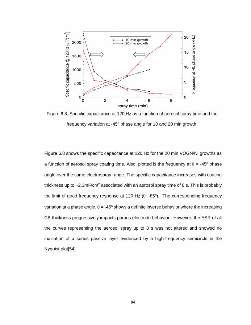
84
Figure 6.8 shows the specific capacitance at 120 Hz for the 20 min VOGN/Ni growths as
a function of aerosol spray coating time. Also, plotted is the frequency at = -45º phase
angle over the same electrospray range. The specific capacitance increases with coating
thickness up to ~2.3mF/cm2 associated with an aerosol spray time of 8 s. This is probably
the limit of good frequency response at 120 Hz (~-85º). The corresponding frequency
variation at a phase angle, = -45º shows a definite inverse behavior where the increasing
CB thickness progressively impacts porous electrode behavior. However, the ESR of all
the curves representing the aerosol spray up to 8 s was not altered and showed no
indication of a series passive layer evidenced by a high-frequency semicircle in the
Nyquist plot[54].
Figure 6.8: Specific capacitance at 120 Hz as a function of aerosol spray time and the
frequency variation at -45º phase angle for 10 and 20 min growth.
85
6.4 Discussion.
6.4.1 RF-PECVD plasma.
The feedstock gases used for this research were 80% C2H2 and 20% H2, at an initial total
pressure of 20 mTorr. A dynamic system (constant pumping) was utilized to insure
removal of reaction products and maintain a constant composition as a function of time.
The plasma strike was generated by 1000W RF supply with an impedance matching
network adjusted to zero reflection. The growth was done at floating potential of ~22 V as
determined by a Langmuir probe. Some pumping by the chamber walls was observed and
this reduced the operational pressure to around 12 mTorr. H2, C4H2, C2H neutrals and
C4H2+m C4H3+ and C2H2+ have been previously detected as the dominant species[34].
Neutral plasma species such as C2nH2 polyacetylenes have been reported[36]. Past
studies of the pure acetylene plasma at 30 mTorr have shown that a large fraction of the
plasma molecules are C4H3 and C2H species[35]. Our studies have suggested the reason
for more rapid growth of the acetylene compared to the methane is the C2H species. The
2-carbon molecule neutral/ ion fits quite nicely into the growing hexagonal array and has
less of a steric issue. This can account for the much faster growth rate over that observed
with the CH4 plasma where the smallest plasma species is the CH molecule/ion. The
impact of the hydrogen atoms and ions on the growth is not known, but the best
morphology of the VOGN was observed with 20% hydrogen either from chemical effects
or energetic erosion[69]. Even from a myriad of suggested plasma components from all
past research, there is still some uncertainty what is the actual growth mechanism[34]–
[36], [39], [69].
86
6.4.2 Ni substrates.
Previous experiments have shown that metals with both a high carbon solubility and a
tendency to dissolve the native surface oxide into the bulk at elevated temperature make
good ohmic bonds to the surface. Ni, Ta and Ti are good examples of this[46].
Furthermore, Ni has a weak oxide bond (NiO) and at the growth temperature of 750ºC in
an ultrahigh vacuum environment all of the oxide/chemisorbed layer decomposes to emit
CO and the remainder dissolves into the bulk[46]. Clearly there is some competitive
regrowth of the oxide at the vacuum level used, but even in the mTorr range, the
dissolution predominates. Sputtering experiments down to the carbon /nickel interface
show no discernible oxygen (<1% using AES). These conditions allow the deposited
carbon to make a good “root” system in the Ni with good conductivity. After the base
carbon layer is formed by the Volmer-Weber thin film mechanism, the carbon growth turns
up at the grain boundaries to form thin vertical sheets. The diffusion of C in Ni is very high
and, during the growth period of even 10 minutes, the C will actually spread laterally in the
Ni bulk to uncoated areas on the periphery of the substrate masked off to form the circular
shape of the thin film VOGN[33]. The ESR of the EDLCs in this work were found to be
between 0.05 and 0.07Ω, completely unaffected by growth of the CB to ~100 nm thick
radius. Generally, the dominant resistance found in EDLCs has an ionic origin and the
electron resistances are negligible.
6.4.3 Carbon coating.
The carbon black coating used in this work was Cabot SC3 which is reported to have
~1800 m2/g surface area. Single electrode capacitance with acetonitrile solvent electrolyte
has been found previously to be 6.8 F/cm3 for a 1µm thick film with area of 1 cm2[68]. Our
film thickness for an 8-s coating time is estimated to be ~100 nm thick or about 1/5 as
87
thick as the above SC3 characteristics. This corresponds to a specific capacitance of
about 1.4 mF/cm2 compared to a measured value of 4.6 mF/cm2 for a single electrode.
Considering the intrinsic surface area of the VOGN to be about a factor of 310 over the
geometric area, one would expect a specific capacity of near 0.1F/cm2. This is a most
conservative estimate. Miller et.al. observed that the aerosol spray did, in fact, end up on
the top edges of the nanosheets so it is a matter of perfecting the method to ultimately
generate a uniform coating and therefore a much higher specific capacitance[44].
6.4.4 Raman data.
The ID/IG ratio previously determined for the uncoated VOGN/Ni architecture was
previously found to be ~0.4. The electrospray coating on this VOGN substrate appeared
to be far less ordered (see figure 6.4), but the Raman spectra observed was not nearly as
high as predicted. As shown in fig 6.5, the ratio went up with coating time but not much
past ID/IG ~1. Further, after the initial increase, the ratio stayed roughly constant which
suggests a rather high density, uniform structure versus coating depth.
6.4.5 Electrochemical impedance measurements.
The EIS measurements showing all the vertical curves in the complex plots indicate that
the CB coatings had little effect on porous electrode behavior because the curves were
near vertical. Also, there was absolutely no passive layer from the absence of a high-
frequency semicircular plot. This shows excellent ohmic bonding of the VOGN to the Ni
surface. The ESR values all fell in the region of 0.05 to 0.07Ω similar to that reported for
that of the uncoated VOGN/Ni[33]. The Bode plots show good frequency response beyond
120Hz indicating these EDLCs are suitable for AC filtering. The thickest coating of 8 s
deposition time resulted in the highest specific capacitance of 2.3 mF/cm2 which is the
highest specific capacitance of an EDLC reported to date. However, that curve was on
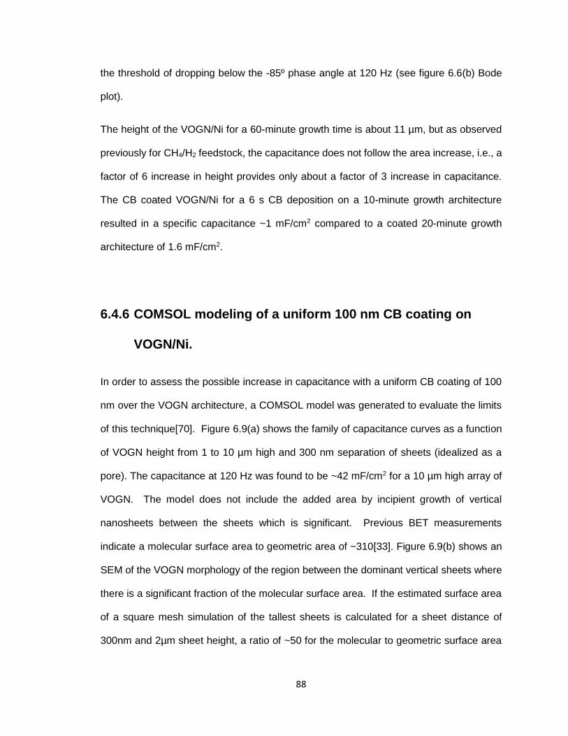
88
the threshold of dropping below the -85º phase angle at 120 Hz (see figure 6.6(b) Bode
plot).
The height of the VOGN/Ni for a 60-minute growth time is about 11 µm, but as observed
previously for CH4/H2 feedstock, the capacitance does not follow the area increase, i.e., a
factor of 6 increase in height provides only about a factor of 3 increase in capacitance.
The CB coated VOGN/Ni for a 6 s CB deposition on a 10-minute growth architecture
resulted in a specific capacitance ~1 mF/cm2 compared to a coated 20-minute growth
architecture of 1.6 mF/cm2.
6.4.6 COMSOL modeling of a uniform 100 nm CB coating on
VOGN/Ni.
In order to assess the possible increase in capacitance with a uniform CB coating of 100
nm over the VOGN architecture, a COMSOL model was generated to evaluate the limits
of this technique[70]. Figure 6.9(a) shows the family of capacitance curves as a function
of VOGN height from 1 to 10 µm high and 300 nm separation of sheets (idealized as a
pore). The capacitance at 120 Hz was found to be ~42 mF/cm2 for a 10 µm high array of
VOGN. The model does not include the added area by incipient growth of vertical
nanosheets between the sheets which is significant. Previous BET measurements
indicate a molecular surface area to geometric area of ~310[33]. Figure 6.9(b) shows an
SEM of the VOGN morphology of the region between the dominant vertical sheets where
there is a significant fraction of the molecular surface area. If the estimated surface area
of a square mesh simulation of the tallest sheets is calculated for a sheet distance of
300nm and 2µm sheet height, a ratio of ~50 for the molecular to geometric surface area
89
ratio is determined. Thus, a conservative estimate of the added area should be at least a
factor of 6, suggesting a capacitance increase of ½ that or 3x the model value of 42
mF/cm2. We could then prognosticate a specific capacitance of ~0.13 F/cm2. Since this
model doesn’t consider the VOGN sheets with stinted growth in the underlying layer, the
predicted capacitance will be even higher. This level of potential capacitance exceeds
commercial viability requirements.
Figure 6.9: (a) COMSOL model estimate of the specific capacitance of uniform 100
nm coating of CB on VOGN at various nanosheet heights. (b) SEM which clearly
shows the significant amount of VOGN undergrowth between the tall sheets, not
included in the COMSOL model.
(b)
120 Hz
(a)
90
6.5 Summary.
This research is a continuation of the work to advance EDLCs as fast response capacitors
capable of AC filtering. The original effort involved using CH4/H2 feedstock in the RF
PECVD system for growing VOGN/Ni that produced nanosheets <1 nm thick, ~600 nm
high in 20-minute growth time. The initial symmetric EDLCs developed in 2010 had a
specific capacitance of 57 µF/cm2 with an RC time constant of less than 200 µs [2]. The
research progression led to C2H2/H2 feedstock EDLCs with few layer graphene
nanosheets (<2 nm thick and ~2 µm high) with a specific capacitance of ~160 µF/cm2 at
750ºC substrate temperature and 265 µF/cm2 at 850ºC substrate temperature (10 minute
VOGN/Ni growth time). Since the VOGN/Ni morphology grown at 850ºC substrate
temperature was somewhat disordered, cauliflower like, with less openness and frequency
response (although good at 120 Hz), the growth at 750ºC substrate temperature was
selected as the better morphology for CB coating[33]. The EDLCs produced in this paper
for CB coatings on both a 10 minute and 20 minute VOGN/Ni architecture resulted in
specific capacitance levels up to 2.3 mF/cm2 at 120 Hz with a phase angle at -85º or better.
This specific capacitance is the highest EDLCs with 120 Hz response reported to date.
These results were achieved with a non-uniform coating of the carbon black where most
of the CB was at the upper edges of the VOGN and formed a crust that inhibited a uniform
coating down to the substrate. It remains a future objective to perfect the coating method.
Since most of the surface area of the VOGN was not coated, the experimental data to
date suggest that a uniform coating of ~100 nm thick on VOGN/Ni 10 µm high over the
entire surface area of the underlying architecture should provide a specific capacitance
greater than ~0.13 F/cm2 with good frequency response at 120 Hz.
91
Chapter 7. Planar interdigitated EDLC design
During the research into VOGN EDLCs, our group collaborated with Cornell Dubilier
capacitor manufacturers in South Carolina, JME Capacitors Inc in Ohio and the US Army
research lab in Maryland, to develop a marketable VOGN EDLC having electrolytic
capacitor level performance. This chapter briefly describes the outcome of this project. To
date, we have always used the typical coin cell design described in the previous chapters
to create the EDLC and obtain the EIS data. This design uses a porous separator
sandwiched between two VOGN electrodes that were grown onto a circular current
collector Ni or Al foil. The typical height of the VOGN are ~1-2 µm and the semi porous
separator is ~25 µm in thickness. The Ni substrates used are 75 µm thick and when
combined, the active material (VOGN) only occupies about 2% of the total volume. To
make this into a more volumetrically efficient device, the planar interdigitated design was
developed by JME Capacitors. A planar design offers volumetric advantages because it
eliminates the need for a separator and reduces the thickness of the current collector.
Figure 7.1 shows the complete assembly of a planar interdigitated capacitor. The
substrate used is an Al2O3(96%) sheet with a Ni coating of ~ 1 µm on top of a Cr stick
layer (0.01 µm thick). VOGN is grown on this Ni layer and then the interdigitated gap is
etched using a YAG laser (Potomac Photonics). The laser ablation cuts through the
VOGN, Ni and the Cr stick layer to the insulating substrate thus making two electrically
isolated electrodes. This required two passes of the laser to produce <20 ohm separation
resistance. The electrolyte was applied on to the top of the VOGN sheets and then the
electrodes
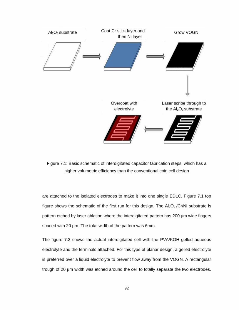
92
Figure 7.1: Basic schematic of interdigitated capacitor fabrication steps, which has a
higher volumetric efficiency than the conventional coin cell design
are attached to the isolated electrodes to make it into one single EDLC. Figure 7.1 top
figure shows the schematic of the first run for this design. The Al2O3 /Cr/Ni substrate is
pattern etched by laser ablation where the interdigitated pattern has 200 µm wide fingers
spaced with 20 µm. The total width of the pattern was 6mm.
The figure 7.2 shows the actual interdigitated cell with the PVA/KOH gelled aqueous
electrolyte and the terminals attached. For this type of planar design, a gelled electrolyte
is preferred over a liquid electrolyte to prevent flow away from the VOGN. A rectangular
trough of 20 µm width was etched around the cell to totally separate the two electrodes.
Al2O3 substrate Coat Cr stick layer and
then Ni layer Grow VOGN
Laser scribe through to
the Al2O3 substrate
Overcoat with
electrolyte
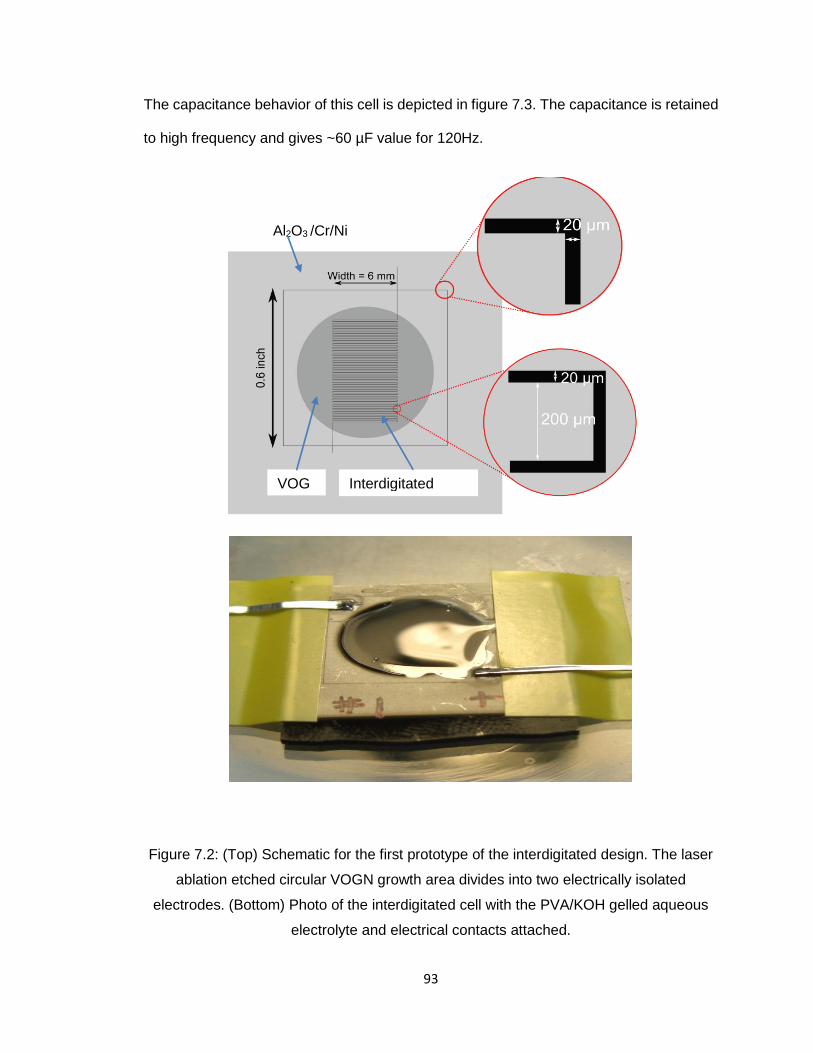
93
The capacitance behavior of this cell is depicted in figure 7.3. The capacitance is retained
to high frequency and gives ~60 µF value for 120Hz.
Figure 7.2: (Top) Schematic for the first prototype of the interdigitated design. The laser
ablation etched circular VOGN growth area divides into two electrically isolated
electrodes. (Bottom) Photo of the interdigitated cell with the PVA/KOH gelled aqueous
electrolyte and electrical contacts attached.
VOG Interdigitated
design
Al2O3 /Cr/Ni
substrate
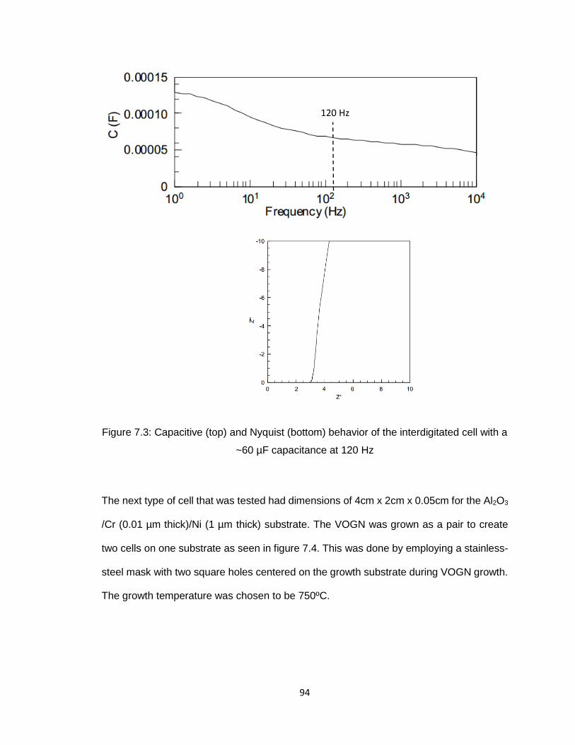
94
Figure 7.3: Capacitive (top) and Nyquist (bottom) behavior of the interdigitated cell with a
~60 µF capacitance at 120 Hz
The next type of cell that was tested had dimensions of 4cm x 2cm x 0.05cm for the Al2O3
/Cr (0.01 µm thick)/Ni (1 µm thick) substrate. The VOGN was grown as a pair to create
two cells on one substrate as seen in figure 7.4. This was done by employing a stainless-
steel mask with two square holes centered on the growth substrate during VOGN growth.
The growth temperature was chosen to be 750ºC.
120 Hz
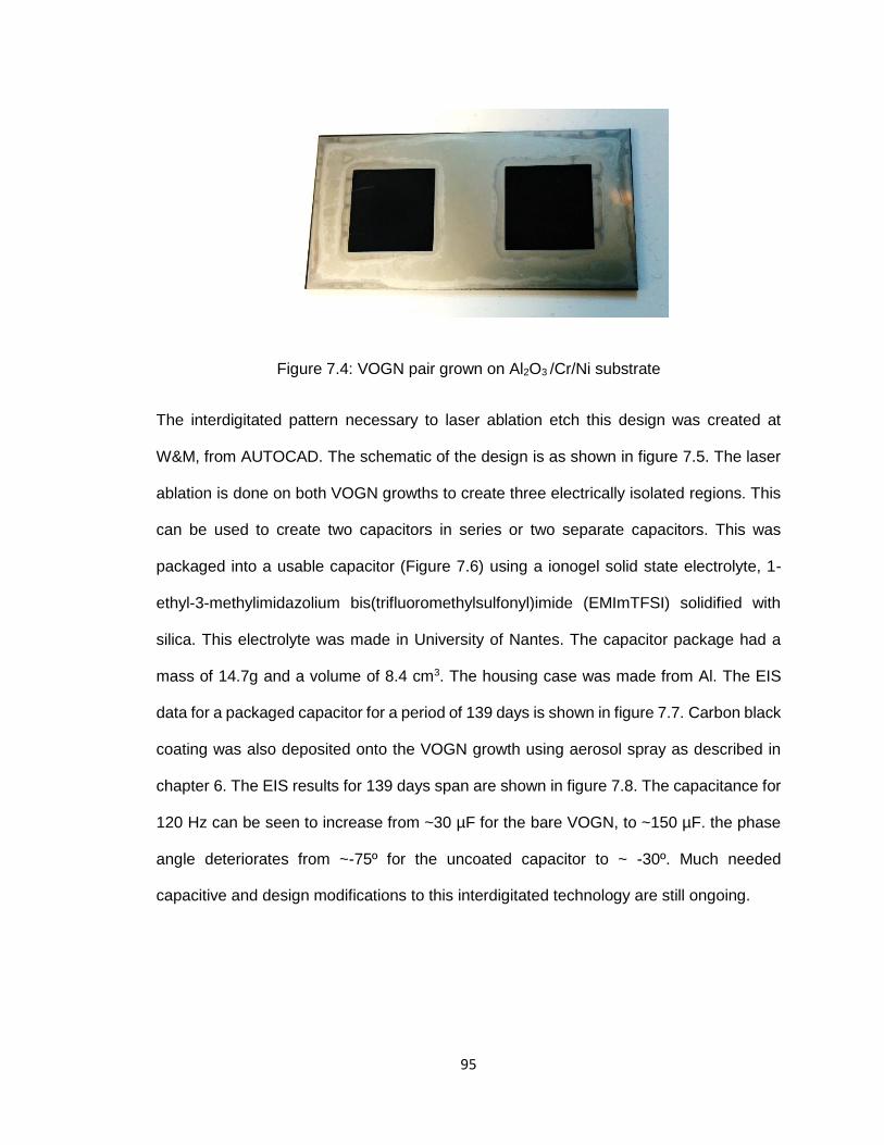
95
Figure 7.4: VOGN pair grown on Al2O3 /Cr/Ni substrate
The interdigitated pattern necessary to laser ablation etch this design was created at
W&M, from AUTOCAD. The schematic of the design is as shown in figure 7.5. The laser
ablation is done on both VOGN growths to create three electrically isolated regions. This
can be used to create two capacitors in series or two separate capacitors. This was
packaged into a usable capacitor (Figure 7.6) using a ionogel solid state electrolyte, 1-
ethyl-3-methylimidazolium bis(trifluoromethylsulfonyl)imide (EMImTFSI) solidified with
silica. This electrolyte was made in University of Nantes. The capacitor package had a
mass of 14.7g and a volume of 8.4 cm3. The housing case was made from Al. The EIS
data for a packaged capacitor for a period of 139 days is shown in figure 7.7. Carbon black
coating was also deposited onto the VOGN growth using aerosol spray as described in
chapter 6. The EIS results for 139 days span are shown in figure 7.8. The capacitance for
120 Hz can be seen to increase from ~30 µF for the bare VOGN, to ~150 µF. the phase
angle deteriorates from ~-75º for the uncoated capacitor to ~ -30º. Much needed
capacitive and design modifications to this interdigitated technology are still ongoing.
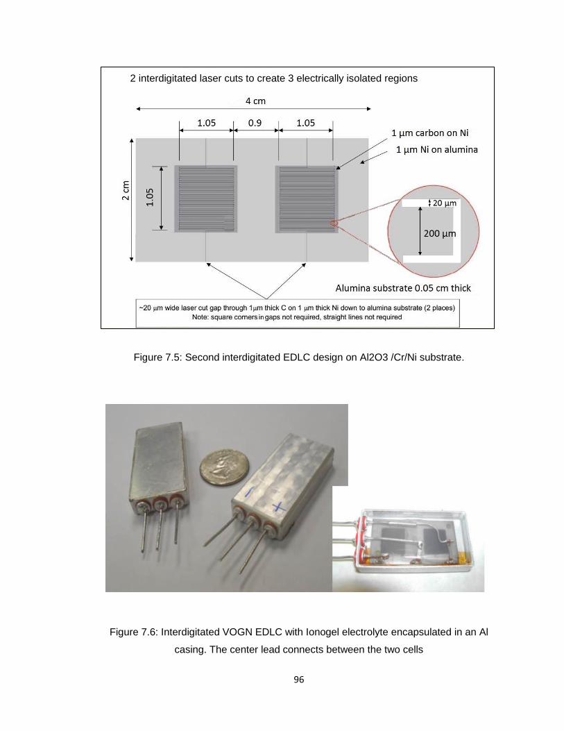
96
Figure 7.5: Second interdigitated EDLC design on Al2O3 /Cr/Ni substrate.
Figure 7.6: Interdigitated VOGN EDLC with Ionogel electrolyte encapsulated in an Al
casing. The center lead connects between the two cells
2 interdigitated laser cuts to create 3 electrically isolated regions
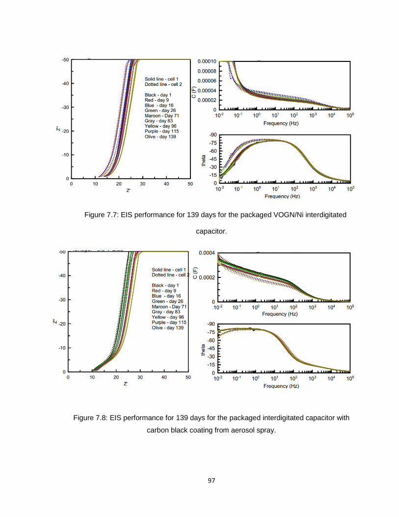
97
Figure 7.7: EIS performance for 139 days for the packaged VOGN/Ni interdigitated
capacitor.
Figure 7.8: EIS performance for 139 days for the packaged interdigitated capacitor with
carbon black coating from aerosol spray.

98
References
This chapter is written based on the presentations done in 46th Power Sources
Conference in Florida (2014) pg. 27, “millisecond – pulse EDLCs” John Miller et al. and
Army SBIR phase 2 final review CDE -August 2014.
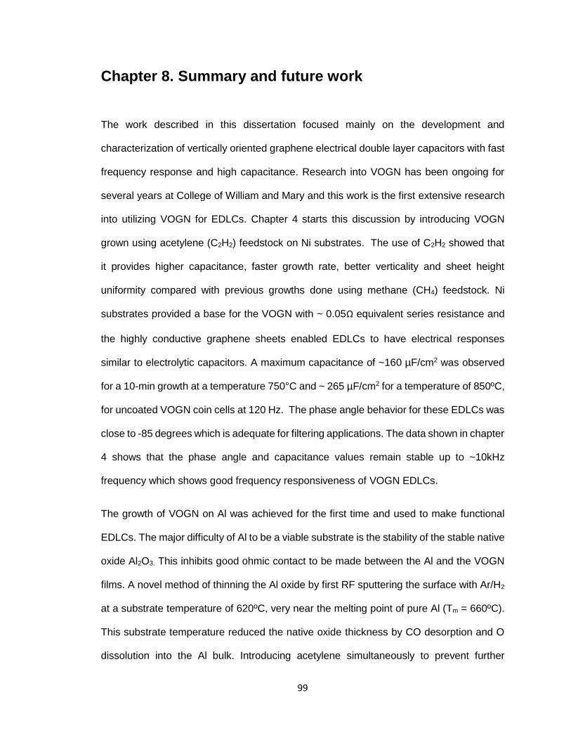
99
Chapter 8. Summary and future work
The work described in this dissertation focused mainly on the development and
characterization of vertically oriented graphene electrical double layer capacitors with fast
frequency response and high capacitance. Research into VOGN has been ongoing for
several years at College of William and Mary and this work is the first extensive research
into utilizing VOGN for EDLCs. Chapter 4 starts this discussion by introducing VOGN
grown using acetylene (C2H2) feedstock on Ni substrates. The use of C2H2 showed that
it provides higher capacitance, faster growth rate, better verticality and sheet height
uniformity compared with previous growths done using methane (CH4) feedstock. Ni
substrates provided a base for the VOGN with ~ 0.05Ω equivalent series resistance and
the highly conductive graphene sheets enabled EDLCs to have electrical responses
similar to electrolytic capacitors. A maximum capacitance of ~160 µF/cm2 was observed
for a 10-min growth at a temperature 750°C and ~ 265 µF/cm2 for a temperature of 850ºC,
for uncoated VOGN coin cells at 120 Hz. The phase angle behavior for these EDLCs was
close to -85 degrees which is adequate for filtering applications. The data shown in chapter
4 shows that the phase angle and capacitance values remain stable up to ~10kHz
frequency which shows good frequency responsiveness of VOGN EDLCs.
The growth of VOGN on Al was achieved for the first time and used to make functional
EDLCs. The major difficulty of Al to be a viable substrate is the stability of the stable native
oxide Al2O3. This inhibits good ohmic contact to be made between the Al and the VOGN
films. A novel method of thinning the Al oxide by first RF sputtering the surface with Ar/H2
at a substrate temperature of 620ºC, very near the melting point of pure Al (Tm = 660ºC).
This substrate temperature reduced the native oxide thickness by CO desorption and O
dissolution into the Al bulk. Introducing acetylene simultaneously to prevent further
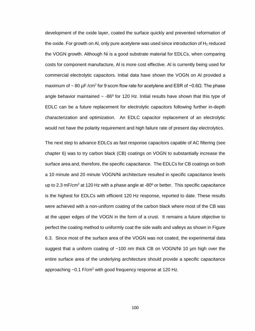
100
development of the oxide layer, coated the surface quickly and prevented reformation of
the oxide. For growth on Al, only pure acetylene was used since introduction of H2 reduced
the VOGN growth. Although Ni is a good substrate material for EDLCs, when comparing
costs for component manufacture, Al is more cost effective. Al is currently being used for
commercial electrolytic capacitors. Initial data have shown the VOGN on Al provided a
maximum of ~ 80 µF /cm2 for 9 sccm flow rate for acetylene and ESR of ~0.6Ω. The phase
angle behavior maintained ~ -86º for 120 Hz. Initial results have shown that this type of
EDLC can be a future replacement for electrolytic capacitors following further in-depth
characterization and optimization. An EDLC capacitor replacement of an electrolytic
would not have the polarity requirement and high failure rate of present day electrolytics.
The next step to advance EDLCs as fast response capacitors capable of AC filtering (see
chapter 6) was to try carbon black (CB) coatings on VOGN to substantially increase the
surface area and, therefore, the specific capacitance. The EDLCs for CB coatings on both
a 10 minute and 20 minute VOGN/Ni architecture resulted in specific capacitance levels
up to 2.3 mF/cm2 at 120 Hz with a phase angle at -80º or better. This specific capacitance
is the highest for EDLCs with efficient 120 Hz response, reported to date. These results
were achieved with a non-uniform coating of the carbon black where most of the CB was
at the upper edges of the VOGN in the form of a crust. It remains a future objective to
perfect the coating method to uniformly coat the side walls and valleys as shown in Figure
6.3. Since most of the surface area of the VOGN was not coated, the experimental data
suggest that a uniform coating of ~100 nm thick CB on VOGN/Ni 10 µm high over the
entire surface area of the underlying architecture should provide a specific capacitance
approaching ~0.1 F/cm2 with good frequency response at 120 Hz.
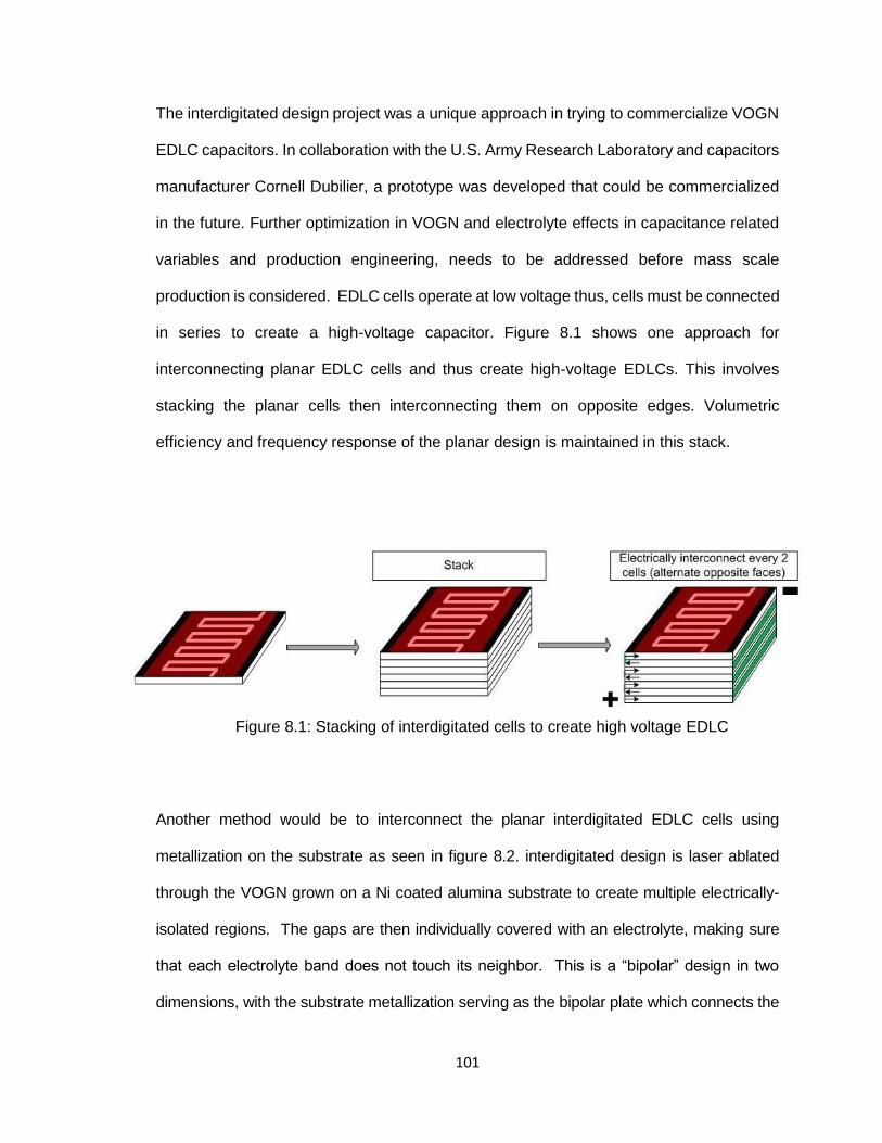
101
The interdigitated design project was a unique approach in trying to commercialize VOGN
EDLC capacitors. In collaboration with the U.S. Army Research Laboratory and capacitors
manufacturer Cornell Dubilier, a prototype was developed that could be commercialized
in the future. Further optimization in VOGN and electrolyte effects in capacitance related
variables and production engineering, needs to be addressed before mass scale
production is considered. EDLC cells operate at low voltage thus, cells must be connected
in series to create a high-voltage capacitor. Figure 8.1 shows one approach for
interconnecting planar EDLC cells and thus create high-voltage EDLCs. This involves
stacking the planar cells then interconnecting them on opposite edges. Volumetric
efficiency and frequency response of the planar design is maintained in this stack.
Figure 8.1: Stacking of interdigitated cells to create high voltage EDLC
Another method would be to interconnect the planar interdigitated EDLC cells using
metallization on the substrate as seen in figure 8.2. interdigitated design is laser ablated
through the VOGN grown on a Ni coated alumina substrate to create multiple electrically-
isolated regions. The gaps are then individually covered with an electrolyte, making sure
that each electrolyte band does not touch its neighbor. This is a “bipolar” design in two
dimensions, with the substrate metallization serving as the bipolar plate which connects the
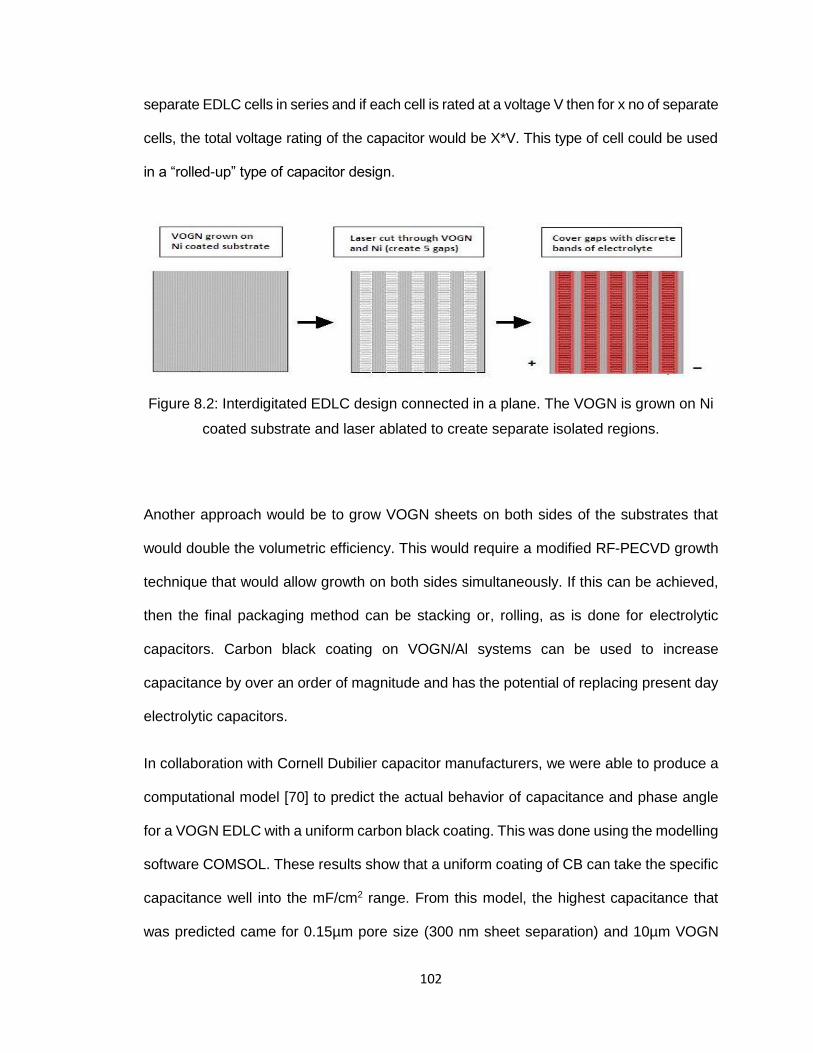
102
separate EDLC cells in series and if each cell is rated at a voltage V then for x no of separate
cells, the total voltage rating of the capacitor would be X*V. This type of cell could be used
in a “rolled-up” type of capacitor design.
Figure 8.2: Interdigitated EDLC design connected in a plane. The VOGN is grown on Ni
coated substrate and laser ablated to create separate isolated regions.
Another approach would be to grow VOGN sheets on both sides of the substrates that
would double the volumetric efficiency. This would require a modified RF-PECVD growth
technique that would allow growth on both sides simultaneously. If this can be achieved,
then the final packaging method can be stacking or, rolling, as is done for electrolytic
capacitors. Carbon black coating on VOGN/Al systems can be used to increase
capacitance by over an order of magnitude and has the potential of replacing present day
electrolytic capacitors.
In collaboration with Cornell Dubilier capacitor manufacturers, we were able to produce a
computational model [70] to predict the actual behavior of capacitance and phase angle
for a VOGN EDLC with a uniform carbon black coating. This was done using the modelling
software COMSOL. These results show that a uniform coating of CB can take the specific
capacitance well into the mF/cm2 range. From this model, the highest capacitance that
was predicted came for 0.15µm pore size (300 nm sheet separation) and 10µm VOGN

103
height coated with 100nm carbon black, was ~42mF/cm2. This model doesn’t consider
any effects from the VOGN undergrowth that contains shorter sheets that has stinted
growths. These sheets have considerable spread across the substrate thus suggesting a
significant contribution to the overall capacitance.
104
References [1] H. I. Becker, “Low voltage electrolytic capacitor,” US Pat. 2,800,616, (1957).
[2] D. L. Boos, “Electrolytic capacitor having carbon paste electrodes,” US Pat. 3536963, (1970).
[3] R. A. Rightmire, “Electrical energy storage apparatus,” US Pat. 3,288,641, (1966).
[4] J. R. Miller, A. F. Burke, J. R. Miller, A. F. Burke, and A. F. Burke, “Electrochemical capacitors: Challenges and opportunities for real-world applications,” Electrochem. Soc., vol. 17, no. 1, pp. 53–57, 2008.
[5] A. G. Pandolfo and A. F. Hollenkamp, “Carbon properties and their role in supercapacitors,” Journal of Power Sources, vol. 157, no. 1. Elsevier, pp. 11–27, Jun-2006.
[6] R. De Levie, “Electrochemical Response of Porous and Rough Electrodes,” in Advances in Electrochemistry and Electrochemical Engineering, 1967, pp. 329–397.
[7] C. Niu, E. K. Sichel, R. Hoch, D. Moy, and H. Tennent, “High power electrochemical capacitors based on carbon nanotube electrodes,” Appl. Phys. Lett., vol. 70, no. 11, pp. 1480–1482, Mar. 1997.
[8] C. Du and N. Pan, “Supercapacitors using carbon nanotubes films by electrophoretic deposition,” J. Power Sources, vol. 160, no. 2, pp. 1487–1494, Oct. 2006.
[9] C. Du and N. Pan, “High power density supercapacitor electrodes of carbon nanotube films by electrophoretic deposition,” Nanotechnology, vol. 17, no. 21, pp. 5314–5318, Nov. 2006.
[10] J.-P. Randin and E. Yeager, “Differential Capacitance Study of Stress-Annealed Pyrolytic Graphite Electrodes,” J. Electrochem. Soc., vol. 118, no. 5, p. 711, 1971.
[11] K. S. Novoselov, “Electric Field Effect in Atomically Thin Carbon Films,” Science (80-. )., vol. 306, no. 5696, pp. 666–669, Oct. 2004.
[12] A. A. Balandin et al., “Superior Thermal Conductivity of Single-Layer Graphene,” Nano Lett., vol. 8, no. 3, pp. 902–907, Mar. 2008.
[13] X. Du, I. Skachko, A. Barker, and E. Y. Andrei, “Approaching ballistic transport in suspended graphene,” Nat. Nanotechnol., vol. 3, no. 8, pp. 491–495, Aug. 2008.
[14] C. Lee, X. Wei, J. W. Kysar, and J. Hone, “Measurement of the Elastic Properties and Intrinsic Strength of Monolayer Graphene,” Science (80-. )., vol. 321, no. 5887, pp. 385–388, Jul. 2008.
[15] H. Helmholtz, “Ueber einige Gesetze der Vertheilung elektrischer Ströme in körperlichen Leitern mit Anwendung auf die thierisch-elektrischen Versuche,” Ann. der Phys. und Chemie, vol. 165, no. 6, pp. 211–233, 1853.
105
[16] D. C. Grahame, “The Electrical Double Layer and the Theory of electrocapillarity.,” Chem. Rev., vol. 41, no. 3, pp. 441–501, Dec. 1947.
[17] M. Gouy, “Sur la constitution de la charge électrique à la surface d’un électrolyte,” J. Phys. Théorique Appliquée, vol. 9, no. 1, pp. 457–468, 1910.
[18] D. L. Chapman, “LI. A contribution to the theory of electrocapillarity,” Philos. Mag. Ser. 6, vol. 25, no. 148, pp. 475–481, Apr. 1913.
[19] O. Stern, “The theory of the electrolytic double shift,” Phys. Chemie, vol. 30, pp. 508–516, 1924.
[20] J. O. Bockris, M. A. V. Devanathan, and K. Muller, “On the Structure of Charged Interfaces,” Proc. R. Soc. A Math. Phys. Eng. Sci., vol. 274, no. 1356, pp. 55–79, Jun. 1963.
[21] F. Beguin, Carbons for electrochemical energy storage and conversion systems. CRC Press, 2010.
[22] R. de Levie, “On porous electrodes in electrolyte solutions,” Electrochim. Acta, vol. 8, no. 10, pp. 751–780, Oct. 1963.
[23] H. Keiser, K. D. Beccu, and M. A. Gutjahr, “Abschätzung der porenstruktur poröser elektroden aus impedanzmessungen,” Electrochim. Acta, vol. 21, no. 8, pp. 539–543, Aug. 1976.
[24] H.-K. Song, Y.-H. Jung, K.-H. Lee, and L. H. Dao, “Electrochemical impedance spectroscopy of porous electrodes: the effect of pore size distribution,” Electrochim. Acta, vol. 44, no. 20, pp. 3513–3519, Jun. 1999.
[25] J. I. Goldstein et al., Scanning Electron Microscopy and X-Ray, vol. 1, no. 3. Kluwer Academic/Plenum Publishers, 2003.
[26] E. Smith and G. Dent, Modern Raman spectroscopy : a practical approach. J. Wiley, 2005.
[27] A. Ferrari and J. Robertson, “Interpretation of Raman spectra of disordered and amorphous carbon,” Phys. Rev. B, vol. 61, no. 20, pp. 14095–14107, 2000.
[28] M. A. Pimenta, G. Dresselhaus, M. S. Dresselhaus, L. G. Cançado, A. Jorio, and R. Saito, “Studying disorder in graphite-based systems by Raman spectroscopy,” Phys. Chem. Chem. Phys., vol. 9, no. 11, pp. 1276–1290, 2007.
[29] A. C. Ferrari and D. M. Basko, “Raman spectroscopy as a versatile tool for studying the properties of graphene,” vol. 8, no. April, 2013.
[30] D. Briggs and M. P. Seah, Practical Surface Analysis volume 1:Auger and X-ray Photoelectron Spectroscopy. Wiley, Chichester, 1983.
[31] P. H. Holloway, “Chemisorption and oxide formation on metals: Oxygen-nickel reaction,” J. Vac. Sci. Technol., vol. 18, no. 2, pp. 653–659, Mar. 1981.
[32] P. H. Holloway and R. A. Outlaw, “The effects of temperature upon NiO formation and oxygen removal on Ni(110),” Surf. Sci., vol. 111, no. 2, pp. 300–316, 1981.
106
[33] M. Cai, R. a. Outlaw, R. a. Quinlan, D. Premathilake, S. M. Butler, and J. R. Miller, “Fast response, vertically oriented graphene nanosheet electric double layer capacitors synthesized from C2H2,” ACS Nano, vol. 8, no. 6, pp. 5873–5882, 2014.
[34] M. J. Vasile and G. Smolinsky, “The chemistry of radiofrequency discharges: Acetylene and mixtures of acetylene with helium, argon and xenon,” Int. J. Mass Spectrom. Ion Phys., vol. 24, no. 1, pp. 11–23, May 1977.
[35] J. R. Doyle, “Chemical kinetics in low pressure acetylene radio frequency glow discharges,” J. Appl. Phys., vol. 82, no. 10, p. 4763, 1997.
[36] J. Benedikt, “Plasma-chemical reactions: low pressure acetylene plasmas,” J. Phys. D. Appl. Phys., vol. 43, no. 4, p. 43001, 2010.
[37] C. Deschenaux, A. Affolter, D. Magni, C. Hollenstein, and P. Fayet, “Investigations of CH4 , C2H2 and C2H4 dusty RF plasmas by means of FTIR absorption spectroscopy and mass spectrometry,” J. Phys. D. Appl. Phys., vol. 32, no. 15, pp. 1876–1886, 1999.
[38] C. Deschenaux, “Etude de l’origine et de la croissance de particules submicrométriques dans les plasmas radiofréquence réactifs,” Jan. 2002.
[39] A. Consoli, J. Benedikt, and A. von Keudell, “Initial Polymerization Reactions in Particle-Forming Ar/He/C2H2 Plasmas Studied via Quantitative Mass Spectrometry,” J. Phys. Chem. A, vol. 112, no. 45, pp. 11319–11329, Nov. 2008.
[40] M. Cai, R. a. Outlaw, S. M. Butler, and J. R. Miller, “A high density of vertically-oriented graphenes for use in electric double layer capacitors,” Carbon N. Y., vol. 50, no. 15, pp. 5481–5488, Dec. 2012.
[41] M. Zhu et al., “A mechanism for carbon nanosheet formation,” Carbon N. Y., vol. 45, no. 11, pp. 2229–2234, Oct. 2007.
[42] A. . Ferrari, J. C. Meyer, C. Scardaci, C. Casiraghi, and M. Lazzeri, “Raman Spectrum of Graphene and Graphene Layers,” Phys. Rev. Lett., vol. 97, no. November, p. 187401 (4), 2006.
[43] J. R. Miller, R. A. Outlaw, and B. C. Holloway, “Graphene Double-Layer Capacitor with ac Line-Filtering Performance,” Science (80-. )., vol. 329, no. 5999, pp. 1637–1639, 2010.
[44] J. R. Miller and R. A. Outlaw, “Vertically-Oriented Graphene Electric Double Layer Capacitor Designs,” J. Electrochem. Soc., vol. 162, no. 5, pp. A5077–A5082, 2015.
[45] C. J. Simensen, “Comments on the solubility of carbon in molten aluminum,” Metall. Trans. A, vol. 20, no. 1, pp. 191–191, Jan. 1989.
[46] M. Cai, R. a. Outlaw, S. M. Butler, and J. R. Miller, “Al (110) surface oxide thermal stability in ultrahigh vacuum,” Surf. Interface Anal., vol. 45, no. 11–12, pp. 1769–1774, 2013.
107
[47] R. T. DeHoff and F. N. Rhines, Quantitative microscopy. McGraw-Hill, New York, 1968.
[48] A. C. Ferrari et al., “Raman spectrum of graphene and graphene layers,” Phys. Rev. Lett., vol. 97, no. 18, pp. 1–4, 2006.
[49] A. C. Ferrari, S. E. Rodil, and J. Robertson, “Interpretation of infrared and Raman spectra of amorphous carbon nitrides,” Phys. Rev. B, vol. 67, no. 15, p. 155306, Apr. 2003.
[50] P. Venezuela, M. Lazzeri, and F. Mauri, “Theory of double-resonant Raman spectra in graphene: Intensity and line shape of defect-induced and two-phonon bands,” Phys. Rev. B - Condens. Matter Mater. Phys., vol. 84, no. 3, pp. 1–25, 2011.
[51] A. Eckmann et al., “Probing the nature of defects in graphene by Raman spectroscopy,” Nano Lett., vol. 12, no. 8, pp. 3925–3930, 2012.
[52] P. Delahay and C. Tobias, Advances In Electrochemistry And Electrochemical Engineering. Interscience Publishers: New York, 1967.
[53] P. L. Taberna, P. Simon, and J. F. Fauvarque, “Electrochemical Characteristics and Impedance Spectroscopy Studies of Carbon-Carbon Supercapacitors,” J. Electrochem. Soc., vol. 150, no. 3, p. A292, 2003.
[54] B. E. Conway, Electrochemical Supercapacitors: Scientific Fundamentals and Technological Applications. Plenum Press: New York, 1999.
[55] F. Tuinstra and J. L. Koenig, “Raman Spectrum of Graphite,” J. Chem. Phys., vol. 53, no. 3, pp. 1126–1130, Aug. 1970.
[56] A. C. Ferrari, “Raman spectroscopy of graphene and graphite: Disorder, electron-phonon coupling, doping and nonadiabatic effects,” Solid State Commun., vol. 143, no. 1–2, pp. 47–57, Jul. 2007.
[57] C. Thomsen and S. Reich, “Double Resonant Raman Scattering in Graphite,” Phys. Rev. Lett., vol. 85, no. 24, pp. 5214–5217, Dec. 2000.
[58] L. M. Malard, M. A. Pimenta, G. Dresselhaus, and M. S. Dresselhaus, “Raman spectroscopy in graphene,” Phys. Rep., vol. 473, no. 5–6, pp. 51–87, 2009.
[59] Y. You, Z. Ni, T. Yu, and Z. Shen, “Edge chirality determination of graphene by Raman spectroscopy,” Appl. Phys. Lett., vol. 93, no. 16, p. 163112, Oct. 2008.
[60] C. Casiraghi et al., “Raman Spectroscopy of Graphene Edges,” Nano Lett., vol. 9, no. 4, pp. 1433–1441, Apr. 2009.
[61] L. G. Cancado, M. A. Pimenta, B. R. A. Neves, M. S. S. Dantas, and A. Jorio, “Influence of the Atomic Structure on the Raman Spectra of Graphite Edges,” Phys. Rev. Lett., vol. 93, no. 24, p. 247401, Dec. 2004.
[62] X. Zhao et al., “Carbon nanosheets as the electrode material in supercapacitors,” J. Power Sources, vol. 194, no. 2, pp. 1208–1212, Dec. 2009.
108
[63] J. R. Miller, R. A. Outlaw, and B. C. Holloway, “Graphene electric double layer capacitor with ultra-high-power performance,” Electrochim. Acta, vol. 56, no. 28, pp. 10443–10449, Dec. 2011.
[64] P. Simon and Y. Gogotsi, “Materials for electrochemical capacitors.,” Nat. Mater., vol. 7, no. 11, pp. 845–54, Nov. 2008.
[65] E. Frackowiak and F. Béguin, “Carbon materials for the electrochemical storage of energy in capacitors,” Carbon N. Y., vol. 39, no. 6, pp. 937–950, May 2001.
[66] K. Sheng, Y. Sun, C. Li, W. Yuan, and G. Shi, “Ultrahigh-rate supercapacitors based on eletrochemically reduced graphene oxide for ac line-filtering.,” Sci. Rep., vol. 2, p. 247, Jan. 2012.
[67] P. Kossyrev, “Carbon black supercapacitors employing thin electrodes,” J. Power Sources, vol. 201, pp. 347–352, Mar. 2012.
[68] “Oljaca, M., Cabot Corporation, Billerica, MA, USA. Personal communication regarding SC3 carbon black.”
[69] M. Bagge-Hansen, R. a. Outlaw, M. Y. Zhu, H. J. Chen, and D. M. Manos, “Hyperthermal atomic hydrogen and oxygen etching of vertically oriented graphene sheets,” J. Vac. Sci. Technol. B Microelectron. Nanom. Struct., vol. 27, no. 6, p. 2413, 2009.
[70] “Dr. Sam Parler - Cornell Dubilier capacitor manufacturers- private communication (2017).” .
109
Vita
Dilshan Viraj Premathilake was born in Kandy, Sri Lanka on September 1983. He
graduated from Trinity College-Kandy in 2002 after sitting for the island wide advanced
level examination and became eligible for university studies in physical science at the
University of Peradeniya. In 2004, he started his Bachelor’s degree in physics and
advanced mathematics. Due to exemplary work, in 2006 he was chosen to do a special
degree in physics minoring in advanced mathematics and graduated in 2008. After a year
of working as a teaching assistant at the University of Peradeniya, he was selected in
August 2009 for graduate studies by the Department of Physics at Old Dominion
University. In 2011, he was awarded a Master of Science in Physics. In August 2012, he
was accepted into the Department of Applied Science Ph.D. program at the College of
William and Mary and began his graduate studies. In January 2013, he began working
with Professor R.A. Outlaw on the VOGN capacitor project. This project included working
with Dr. J.R. Miller of Case Western Reserve University and Mr. S.G Parler of Cornell
Dubilier Electronics.
Related Documents