ARTICLES PUBLISHED ONLINE: 28 SEPTEMBER 2014 | DOI: 10.1038/NMAT4091 Vertical and in-plane heterostructures from WS 2 /MoS 2 monolayers Yongji Gong 1,2† , Junhao Lin 3,4† , Xingli Wang 5,6† , Gang Shi 2 , Sidong Lei 2 , Zhong Lin 7 , Xiaolong Zou 2 , Gonglan Ye 2 , Robert Vajtai 2 , Boris I. Yakobson 2 , Humberto Terrones 8 , Mauricio Terrones 7,9,10,11 , Beng Kang Tay 5,6 , Jun Lou 2 , Sokrates T. Pantelides 3,4 , Zheng Liu 5,6 , Wu Zhou 3 * and Pulickel M. Ajayan 1,2 * Layer-by-layer stacking or lateral interfacing of atomic monolayers has opened up unprecedented opportunities to engineer two-dimensional heteromaterials. Fabrication of such artificial heterostructures with atomically clean and sharp interfaces, however, is challenging. Here, we report a one-step growth strategy for the creation of high-quality vertically stacked as well as in-plane interconnected heterostructures of WS 2 /MoS 2 via control of the growth temperature. Vertically stacked bilayers with WS 2 epitaxially grown on top of the MoS 2 monolayer are formed with preferred stacking order at high temperature. A strong interlayer excitonic transition is observed due to the type II band alignment and to the clean interface of these bilayers. Vapour growth at low temperature, on the other hand, leads to lateral epitaxy of WS 2 on MoS 2 edges, creating seamless and atomically sharp in-plane heterostructures that generate strong localized photoluminescence enhancement and intrinsic p–n junctions. The fabrication of heterostructures from monolayers, using simple and scalable growth, paves the way for the creation of unprecedented two-dimensional materials with exciting properties. H eterostructures have been the essential elements in modern semiconductor industry, and play a crucial role in high- speed electronics and optoelectronic devices 1,2 . Beyond conventional semiconductors, two-dimensional (2D) materials provide a wide range of basic building blocks with distinct optical and electrical properties, including graphene 3 , hexagonal boron nitride 4,5 and transition-metal dichalcogenides (TMDs; refs 6–9). These atomic monolayers could also be combined to create van der Waals heterostructures, where monolayers of multiple 2D materials are stacked vertically layer-by-layer, or stitched together seamlessly in-plane to form lateral heterojunctions. Many physical properties have been explored on such van der Waals heterostructures, and devices with improved performance have been demonstrated 10–14 . The lateral heterojunctions could also lead to exciting new physics and applications. For example, the semiconducting monolayer TMDs can serve as building blocks for p–n junctions and other optoelectronic devices 15–17 . However, the fabrication of 2D heterostructures with clean and sharp interfaces, essential for preserving optoelectronic properties driven by the interlayer or intralayer coupling, remains challenging. Van der Waals heterostructures could be created by stacking different 2D materials using mechanical transfer techniques 12 . However, the stacking orientation cannot be precisely controlled, the interface between layers can be easily contaminated 18,19 , and there are significant challenges for massive production of the samples. Lateral heterostructures, in contrast, can be created only via growth. Both vertical and in-plane heterostructures of semi-metallic graphene and insulating hexagonal boron nitride have recently been demonstrated via chemical vapour deposition (CVD; refs 20–24); however, direct growth of heterostructures consisting of different semiconducting monolayers has not been achieved. Here, we report a scalable single-step vapour phase growth process for the creation of highly crystalline vertical stacked bilayers and in-plane interconnected WS 2 /MoS 2 heterostructures, respectively, under different growth temperatures. Atomic- resolution scanning transmission electron microscopy (STEM) imaging reveals that high-temperature growth yields predominantly vertically stacked bilayers with WS 2 epitaxially grown on top of the MoS 2 monolayer, following the preferred 2H stacking. In contrast, low-temperature growth creates mostly lateral heterostructures of WS 2 and MoS 2 within a single hexagonal monolayer lattice, with atomically sharp heterojunctions along both the zigzag and armchair directions. The vertical and lateral heterostructures are further verified by Raman and photoluminescence (PL) spectroscopy characterization. Strong interlayer or intralayer excitonic interactions between MoS 2 and WS 2 are observed by PL spectroscopy for the first time on these two types of heterostructures, owing to their clean and sharp interfaces. 1 Department of Chemistry, Rice University, Houston, Texas 77005, USA, 2 Department of Materials Science and NanoEngineering, Rice University, Houston, Texas 77005, USA, 3 Materials Science and Technology Division, Oak Ridge National Lab, Oak Ridge, Tennessee 37831, USA, 4 Department of Physics and Astronomy, Vanderbilt University, Nashville, Tennessee 37235, USA, 5 School of Materials Science and Engineering, Nanyang Technological University, Singapore 639798, 6 School of Electrical and Electronic Engineering, Nanyang Technological University, Singapore 639798, 7 Department of Physics and Center for 2-Dimensional and Layered Materials, The Pennsylvania State University, University Park, Pennsylvania 16802, USA, 8 Department of Physics, Applied Physics and Astronomy, Rensselaer Polytechnic Institute, Johnson-Rowland Science Center, 110 Eighth Street, Troy, New York 12180, USA, 9 Department of Chemistry, The Pennsylvania State University, University Park, Pennsylvania 16802, USA, 10 Department of Materials Science and Engineering, The Pennsylvania State University, University Park, Pennsylvania 16802, USA, 11 Materials Research Institute, The Pennsylvania State University, University Park, Pennsylvania 16802, USA. † These authors contributed equally to this work. *e-mail: [email protected]; [email protected] NATURE MATERIALS | ADVANCE ONLINE PUBLICATION | www.nature.com/naturematerials 1 © 2014 Macmillan Publishers Limited. All rights reserved.

Welcome message from author
This document is posted to help you gain knowledge. Please leave a comment to let me know what you think about it! Share it to your friends and learn new things together.
Transcript
ARTICLESPUBLISHED ONLINE: 28 SEPTEMBER 2014 | DOI: 10.1038/NMAT4091
Vertical and in-plane heterostructures fromWS2/MoS2 monolayersYongji Gong1,2†, Junhao Lin3,4†, Xingli Wang5,6†, Gang Shi2, Sidong Lei2, Zhong Lin7, Xiaolong Zou2,Gonglan Ye2, Robert Vajtai2, Boris I. Yakobson2, Humberto Terrones8, Mauricio Terrones7,9,10,11,Beng Kang Tay5,6, Jun Lou2, Sokrates T. Pantelides3,4, Zheng Liu5,6, Wu Zhou3*and Pulickel M. Ajayan1,2*
Layer-by-layer stacking or lateral interfacing of atomic monolayers has opened up unprecedented opportunities to engineertwo-dimensional heteromaterials. Fabrication of such artificial heterostructures with atomically clean and sharp interfaces,however, is challenging. Here, we report a one-step growth strategy for the creation of high-quality vertically stacked as well asin-plane interconnected heterostructures ofWS2/MoS2 via control of the growth temperature. Vertically stacked bilayers withWS2 epitaxially grown on top of the MoS2 monolayer are formed with preferred stacking order at high temperature. A stronginterlayer excitonic transition is observed due to the type II band alignment and to the clean interface of these bilayers. Vapourgrowth at low temperature, on the other hand, leads to lateral epitaxy ofWS2 onMoS2 edges, creating seamless and atomicallysharp in-plane heterostructures that generate strong localized photoluminescence enhancement and intrinsic p–n junctions.The fabrication of heterostructures from monolayers, using simple and scalable growth, paves the way for the creation ofunprecedented two-dimensional materials with exciting properties.
Heterostructures have been the essential elements in modernsemiconductor industry, and play a crucial role in high-speed electronics and optoelectronic devices1,2. Beyond
conventional semiconductors, two-dimensional (2D) materialsprovide a wide range of basic building blocks with distinct opticaland electrical properties, including graphene3, hexagonal boronnitride4,5 and transition-metal dichalcogenides (TMDs; refs 6–9).These atomic monolayers could also be combined to createvan der Waals heterostructures, where monolayers of multiple2D materials are stacked vertically layer-by-layer, or stitchedtogether seamlessly in-plane to form lateral heterojunctions. Manyphysical properties have been explored on such van der Waalsheterostructures, and devices with improved performance havebeen demonstrated10–14. The lateral heterojunctions could alsolead to exciting new physics and applications. For example, thesemiconducting monolayer TMDs can serve as building blocks forp–n junctions and other optoelectronic devices15–17. However, thefabrication of 2D heterostructures with clean and sharp interfaces,essential for preserving optoelectronic properties driven by theinterlayer or intralayer coupling, remains challenging. Van derWaals heterostructures could be created by stacking different 2Dmaterials using mechanical transfer techniques12. However, thestacking orientation cannot be precisely controlled, the interfacebetween layers can be easily contaminated18,19, and there are
significant challenges for massive production of the samples.Lateral heterostructures, in contrast, can be created only viagrowth. Both vertical and in-plane heterostructures of semi-metallicgraphene and insulating hexagonal boron nitride have recently beendemonstrated via chemical vapour deposition (CVD; refs 20–24);however, direct growth of heterostructures consisting of differentsemiconducting monolayers has not been achieved.
Here, we report a scalable single-step vapour phase growthprocess for the creation of highly crystalline vertical stackedbilayers and in-plane interconnected WS2/MoS2 heterostructures,respectively, under different growth temperatures. Atomic-resolution scanning transmission electron microscopy (STEM)imaging reveals that high-temperature growth yields predominantlyvertically stacked bilayers with WS2 epitaxially grown on top of theMoS2 monolayer, following the preferred 2H stacking. In contrast,low-temperature growth creates mostly lateral heterostructuresof WS2 and MoS2 within a single hexagonal monolayer lattice,with atomically sharp heterojunctions along both the zigzag andarmchair directions. The vertical and lateral heterostructuresare further verified by Raman and photoluminescence (PL)spectroscopy characterization. Strong interlayer or intralayerexcitonic interactions between MoS2 and WS2 are observedby PL spectroscopy for the first time on these two types ofheterostructures, owing to their clean and sharp interfaces.
1Department of Chemistry, Rice University, Houston, Texas 77005, USA, 2Department of Materials Science and NanoEngineering, Rice University,Houston, Texas 77005, USA, 3Materials Science and Technology Division, Oak Ridge National Lab, Oak Ridge, Tennessee 37831, USA, 4Department ofPhysics and Astronomy, Vanderbilt University, Nashville, Tennessee 37235, USA, 5School of Materials Science and Engineering, Nanyang TechnologicalUniversity, Singapore 639798, 6School of Electrical and Electronic Engineering, Nanyang Technological University, Singapore 639798, 7Department ofPhysics and Center for 2-Dimensional and Layered Materials, The Pennsylvania State University, University Park, Pennsylvania 16802, USA, 8Departmentof Physics, Applied Physics and Astronomy, Rensselaer Polytechnic Institute, Johnson-Rowland Science Center, 110 Eighth Street, Troy, New York 12180,USA, 9Department of Chemistry, The Pennsylvania State University, University Park, Pennsylvania 16802, USA, 10Department of Materials Science andEngineering, The Pennsylvania State University, University Park, Pennsylvania 16802, USA, 11Materials Research Institute, The Pennsylvania StateUniversity, University Park, Pennsylvania 16802, USA. †These authors contributed equally to this work. *e-mail: [email protected]; [email protected]
NATURE MATERIALS | ADVANCE ONLINE PUBLICATION | www.nature.com/naturematerials 1© 2014 Macmillan Publishers Limited. All rights reserved.
ARTICLES NATUREMATERIALS DOI: 10.1038/NMAT4091
850 °C
Te + W MoO3 S powder
Quartz tube
WS2
WS2
MoS2
MoS2
SiO2
SiO2
SiO2/Si
Vertical WS2/MoS2 bilayer
In-plane WS2 /MoS2 monolayer
650 °C
a b c d
e
i
f g h
5 µm 5 µm40 µm
10 µm 5 µm 5 µm
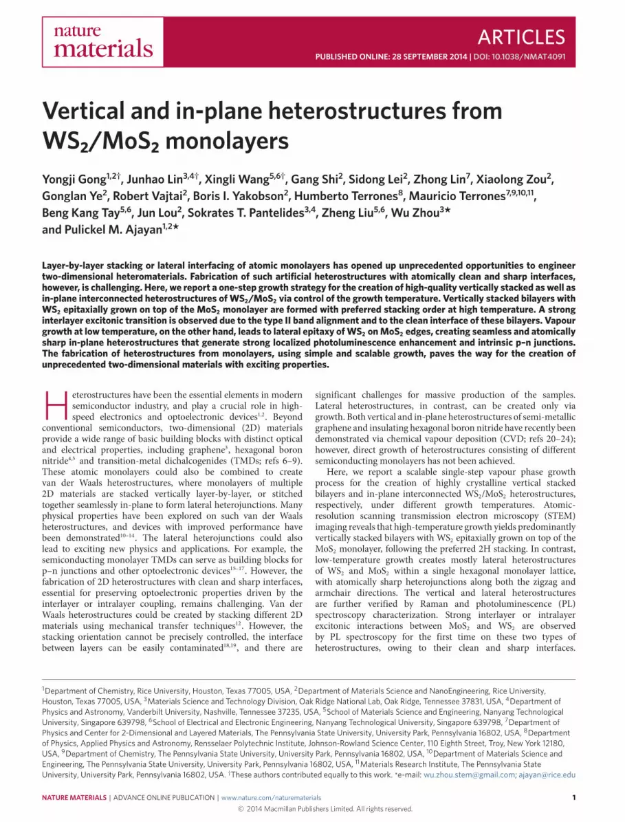
Figure 1 | Schematic of the synthesis and the overall morphologies of the vertically stacked and in-plane WS2/MoS2 heterostructures. a–d, Schematic,optical and SEM images of the vertically stacked WS2/MoS2 heterostructures synthesized at 850 ◦C, showing the bilayer feature and the high yield of thetriangular heterostructures. e–h, Schematic, optical and SEM images of the WS2/MoS2 in-plane heterojunctions grown at 650 ◦C. g is an optical imageof the interface between WS2 and MoS2 with enhanced colour contrast, showing the abrupt change of contrast at the interface. SEM images are presentedin reverse contrast. The green, purple and yellow spheres in a,e represent W, Mo and S atoms, respectively. i, Schematic of the synthesis process forboth heterostructures.
Specifically, a bandgap of 1.42 eV is observed in the bilayerheterostructure, arising from the interlayer excitonic transitionbetween MoS2 and WS2 (refs 25,26); whereas a strong localizedPL enhancement is observed at the lateral interface between MoS2and WS2, presumably due to the increased excitonic recombinationof the as-generated electron–hole pairs at the atomically sharpinterface27. These two types of heterostructures are furtherdemonstrated to be building blocks for high-mobility field-effecttransistors (FET) and planar monolayer p–n junctions, indicatingtheir potential for constructing unique devices.
Synthesis and morphologyFigure 1i shows the scheme for the growth of WS2/MoS2 het-erostructures. Molybdenum trioxide (MoO3) powder is placed infront of the bare SiO2/Si wafer for the growth of MoS2, while amixed powder of tungsten and tellurium is scattered on the waferfor the growth of WS2. The addition of tellurium helps to acceleratethe melting of tungsten powder during the growth (SupplementaryFig. 4). Sulphur powder is put upstreamwithin the low-temperaturezone. Argon is used to protect the system from oxygen and carrysulphur vapour from the upstream of the tube during the reaction.The difference in their nucleation and growth rates gives rise tosequential growth of MoS2 and WS2, instead of MoxW1−xS2 alloy,and the precise reaction temperature determines the structure of thefinal product: vertically stacked bilayers are preferred at ∼850 ◦C,whereas in-plane lateral heterojunctions dominate when thesynthesis is carried out at∼650 ◦C (see Supplementary Informationfor more details). A brief discussion of the possible mechanism ofthe temperature-selective growth is provided in the SupplementaryInformation. This simple, scalable growth process creates cleaninterfaces between the twomonolayer components, which is advan-tageous over mechanical transfer of layers.
The morphology of the WS2/MoS2 vertical and in-planeheterostructures was examined by optical microscopy, scanning
electron microscopy (SEM) and atomic force microscopy (AFM).Figure 1a–d are the schematic and typical optical and SEMimages of the vertically stacked heterostructures, showing individualWS2/MoS2 bilayer triangles and a high yield of heterostructures.The bilayers can be easily distinguished from monolayers viaoptical contrast (Fig. 1b), with MoS2 monolayers showing a lightpurple colour and the bilayer regions as much darker purple.The domain size of the bottom MoS2 layer is typically largerthan 10 µm. Both totally covered and partially covered WS2/MoS2bilayers (Supplementary Fig. 5) can be found, providing differentgeometries for device fabrication. The schematics and morphologyof WS2/MoS2 in-plane heterostructures are shown in Fig. 1e–h,where the lateral interface between monolayer MoS2 and WS2can be easily distinguished by the contrast difference. Optical andSEM images shown in Supplementary Fig. 6 demonstrate the highyield of such in-plane heterostructures obtained from this growthmethod. The difference in bilayer or monolayer morphology ofthese two types of heterostructures is further verified by AFMimages presented in Supplementary Fig. 7.
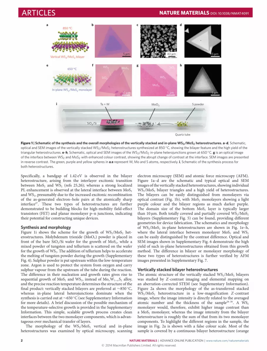
Vertically stacked bilayer heterostructuresThe atomic structure of the vertically stacked WS2/MoS2 bilayerswas studied by Z-contrast imaging and elemental mapping onan aberration-corrected STEM (see Supplementary Information).Figure 2a shows the morphology of the as-transferred stackedWS2/MoS2 heterostructure in a low-magnification Z-contrastimage, where the image intensity is directly related to the averagedatomic number and the thickness of the sample28–30. A WS2monolayer would, therefore, exhibit higher image contrast thana MoS2 monolayer, whereas the image intensity from the bilayerheterostructure is roughly the sum of that from its two monolayercomponents. To highlight the different regions in the sample, theimage in Fig. 2a is shown with a false colour scale. Most of thesample is covered by a continuous bilayer heterostructure (orange
2 NATURE MATERIALS | ADVANCE ONLINE PUBLICATION | www.nature.com/naturematerials© 2014 Macmillan Publishers Limited. All rights reserved.
NATUREMATERIALS DOI: 10.1038/NMAT4091 ARTICLES
Mo map S mapW map
0
Intensity (a.u.)
1
50 nm 5 nm
1 nm
1 nm
0.0
a
c
e f g
d
b
0.0 0.5Distance (nm)
1.0 1.5
0.2
0.4
0.6
0.8
1.0
Inte
nsity
(a.u
.)In
tens
ity (a
.u.)
0 5 10 15Distance (nm)
MoS2
Mo + S2 Mo + S2
S2 + W
S2 + Mo
S2 + W
Mo + S2
MoS2/WS2
WS2
20 25 30
Figure 2 | STEM Z-contrast imaging and elemental mapping of the stacked WS2/MoS2 heterostructures. a, Low-magnification false-colour Z-contrastimage of the sample, where monolayer MoS2 is shown in blue, monolayer WS2 in green, and the WS2/MoS2 bilayer in orange. b, Zoom-in view of theregion outlined by the square in a. c, Z-contrast image intensity profile along the dashed line in b, showing the distinct contrast variation among thedi�erent monolayer and bilayer regions. d, Elemental mapping of Mo, W and S from the whole area shown in b. e, Top: Z-contrast image of the bilayerregion with a 2H stacking orientation. The brighter columns are overlapping columns of W and S2, whereas the less bright columns are overlapping of S2and Mo. The green arrow points to the atomic positions where a W atom is replaced by a Mo atom in the WS2 layer, which has a similar intensity to itsneighbouring site. Bottom: Image intensity profile acquired along the yellow rectangle in the image above. f, Z-contrast image of the step edge of theWS2/MoS2 bilayer. The green dashed line indicates the step edge, and the two triangles indicate the orientation of the MoS2 (top part of image) and WS2(bottom part) layers. Inset: Fast Fourier transform of the Z-contrast image showing only one set of di�raction patterns. g, Schematic of the 2H stacking inthe stacked WS2/MoS2 heterostructure.
region), while at some intentionally induced broken edges (seeSupplementary Information) both of the individual monolayers canbe identified (with MoS2 shown in blue and WS2 shown in green).Figure 2b shows amagnified image of the region outlined by a squarein Fig. 2a. The obvious contrast step across the two individual layers,as shown by the image intensity line profile in Fig. 2c, demonstratesthe presence of separated MoS2 and WS2 monolayers instead ofa homogeneous MoxW1−xS2 alloy. Elemental mapping of Mo, Wand S (Fig. 2d and Supplementary Fig. 8) from the same regionunambiguously confirms thatMoS2 andWS2 are well separated intotwo atomic layers, forming vertical bilayer heterostructures.
Figure 2e,f shows atomic-resolution Z-contrast images from thebilayer region and a step edge of the WS2/MoS2 heterostructure,
respectively. The alternative bright and dark atomic columnarrangement in the hexagonal lattice suggests the as-grown stackedWS2/MoS2 heterostructure preserves the 2H stacking, where thebright and dark columns are W and Mo atom-aligned with aS2 column, respectively, as illustrated in Fig. 2g. The WS2/MoS2heterostructure grown by our one-step growth method is foundto have predominantly the 2H stacking, which exemplifies theadvantage of this direct growthmethod over themechanical transfermethod, where the stacking orientation of the heterostructurecannot be well controlled. As a side note, Mo substitution in theWS2 layer can occasionally be observed, as indicated by the reducedcontrast at the W atomic sites (green arrows in Fig. 2e and theassociated intensity line profile). Similarly, some trace amount of
NATURE MATERIALS | ADVANCE ONLINE PUBLICATION | www.nature.com/naturematerials 3© 2014 Macmillan Publishers Limited. All rights reserved.
ARTICLES NATUREMATERIALS DOI: 10.1038/NMAT4091
2
2
4
4
3
3
1
1
10 µm
10 µm10 µm
Raman shift (cm−1)480
600 700 800Wavelength (nm)
900
1
2
3
4
320
Inte
nsity
(a.u
.)
Inte
nsity
(a.u
.)
Inte
nsity
(a.u
.)
Dra
in c
urre
nt (n
A)
WS2 2LA(M)
MoS2 E’ MoS2 A1’
WS2 A1’
WS2/MoS2 CVD growthWS2/MoS2 transferredWS2/MoS2 CVD growth
MoS2 bilayerWS2 bilayer
WS2/MoS2 transferred
MoS2 monolayer
MoS2 bilayer
and E’
340 360 380 400 420 440 460
10 µm
384 cm−1
357 cm−1
680 nm
3,000
2,500
2,000
1,500
1,000
500
0
1,0000
100
200
300
400
500
600
1
2
3
4630
680 875
680 nm
10 µm
600 700 800 900Wavelength (nm) Gate voltage (V)
−20 −10 0 10 20
3,5003,000
2,000
a b c
d e f
g h i
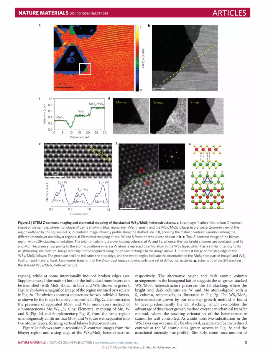
Figure 3 | Raman and PL characterization of the WS2/MoS2 vertical heterostructure. a, Optical image of a WS2/MoS2 heterostructure used for Ramancharacterization. b, Raman spectra taken from the four points marked in a, showing that the monolayer region is pure MoS2, whereas the double layer areais the superposition of MoS2 and WS2 monolayers. The dashed lines are guides to the eye showing the position of the MoS2 and WS2 Raman peaks.c,d, Raman intensity mapping at 384 cm−1 and 357 cm−1, respectively. The lower Raman intensity at the centre of the triangle in c is due to the coverage ofWS2. e, Optical image of a WS2/MoS2 heterostructure used for PL characterization. f, PL Spectra taken from the four points marked in e, showing thecharacteristic MoS2 PL peak at the monolayer region and three peaks at the bilayer region. g, PL intensity mapping at 680 nm shows localized PLenhancement around the step edge of the bilayer region. h, PL spectra of a CVD-grown WS2/MoS2 bilayer, a WS2/MoS2 bilayer made by mechanicaltransfer, and CVD-grown MoS2 and WS2 bilayers. All spectra were taken at the same laser intensity and plotted to the same scale. The PL peak at 875 nmis absent in the mechanically transferred bilayer sample, and the bilayer MoS2 and WS2 have a very weak PL response owing to their indirect bandgap.i, Typical plot of gating voltage versus source/drain current of a CVD-grown WS2/MoS2 bilayer, a mechanically transferred WS2/MoS2 bilayer, a MoS2bilayer and monolayer MoS2 demonstrating that the CVD-grown WS2/MoS2 bilayer has the best performance.
W atoms is also found to substitute into the MoS2 layer (Fig. 2f).However, the substitution is at a fairly low concentration (∼3%, seeSupplementary Fig. 9 for details), which would have only a minimaleffect on the properties of the MoS2 and WS2 monolayers.
Raman and PL spectroscopy were used to further characterizethe vertical bilayer heterostructure. As shown in Fig. 3a,b, Ramanspectra collected from the light purple area (points 1 and 2) showonly the E′ (at 383.9 cm−1) and A′1 (at 405.3 cm−1) peaks of theMoS2monolayer8,9, confirming the bottom layer is MoS2 (ref. 31). In thebilayer region (points 3 and 4 in the dark purple area), however, twoadditional peaks located at 418.5 cm−1 and 356.8 cm−1 are observed,which can be assigned to the A′1 mode and the overlapping 2LA(M)and E′ modes, respectively, of the top WS2 monolayer6,32 (details inSupplementary Fig. 10). Raman intensity mapping using the MoS2E′ mode at 384 cm−1 and the WS2 E′ mode at 357 cm−1 furtherdemonstrate the formation of WS2/MoS2 bilayer stacks, as shownin Fig. 3c,d.
The PL spectra (Fig. 3f) acquired from the monolayer region(points 1 and 2 in Fig. 3e) show a strong peak only at a wavelength
of 680 nm, corresponding to the 1.82 eV direct excitonic transitionenergy in monolayer MoS2. However, on the bilayer region (points3 and 4), three prominent peaks are observed at wavelengths of630 nm, 680 nm and 875 nm, corresponding to excitonic transitionenergies of 1.97 eV, 1.82 eV and 1.42 eV, respectively. The peaks at630 nm (1.97 eV) and 680 nm (1.82 eV) can be attributed to thedirect excitonic transition energies in the topWS2 and bottomMoS2monolayers, respectively. It has been reported that the increasedindirect excitonic transition in multilayer WS2 and MoS2 (refs 7,33)can generate small peaks at a similar lower transition energy range.The intensity of such indirect excitonic peaks, however, is more thanthree orders of magnitude lower than the direct excitonic peak frommonolayers. The comparable intensity of the peak at 875 nm to thatof its individual monolayer components observed in our bilayersample, as shown in Fig. 3f, indicates a possible direct excitonictransition at this energy range. Such a strong direct excitonic peakat 875 nm (1.42 eV) is indeed observed for the first time in thisbilayer heterostructure. This experimental observation is consistentwith previous theoretical calculations, which suggest the coupling
4 NATURE MATERIALS | ADVANCE ONLINE PUBLICATION | www.nature.com/naturematerials© 2014 Macmillan Publishers Limited. All rights reserved.
NATUREMATERIALS DOI: 10.1038/NMAT4091 ARTICLESbetween the WS2 and MoS2 layers leads to an unprecedented directbandgap with reduced energy25,26. Supplementary Fig. 11 showsthe PL intensity mapping at 875 nm, confirming the intensity islocalized at the bilayer region. Notably, the PL signal from MoS2 at680 nm shows a localized enhancement near the step edges betweenthe monolayer and bilayer regions, as shown in Fig. 3g and furtherillustrated by the PL intensity line profile shown in SupplementaryFig. 12. The PL enhancement is also demonstrated by analysingthe PL spectra extracted from the step-edge region (point 1) andthe edge of the MoS2 monolayer (point 2 in Fig. 3e), showingalmost twice the difference in intensity. This step-edge enhancementis distinctly different from the previous reported edge-enhanced6
or homogeneous34 PL response in monolayer TMDs, and may becaused by the interaction between the MoS2 and WS2 layers.
As a comparison, Raman and PL measurements were alsoperformed on a stacked WS2/MoS2 heterostructure, made by thecommonly-usedmechanical transfermethod, and on a CVD-grownMoS2/WS2 bilayer (Fig. 3h and Supplementary Fig. 13). Althoughthe Raman spectra are similar to the WS2/MoS2 bilayer fromdirect growth (Supplementary Fig. 13), the additional PL peakat 875 nm, originating from an interlayer excitonic transition25,26,is absent in the PL spectra from the mechanically transfer-stacked bilayer sample, presumably owing to contamination at theinterface during the mechanical transfer of the two layers. Thispeak at 875 nm should also be observable in transferred layersif a contamination-free interface could be achieved. These resultshighlight the advantage of using our CVD method for the directgrowth of crystalline heterostructures, in which layer transfers arenot needed and a clean interface could be readily obtained. Inaddition, the 1.82 eV (680 nm) and 1.97 eV (630 nm) PL peaksobserved in the stackedWS2/MoS2 bilayer almost vanish in a CVD-grown MoS2 bilayer and WS2 bilayer7. This observation suggeststhat the MoS2 and WS2 layers in the bilayer heterostructure, onone hand, behave as individual monolayers and, on the other hand,generate new functionalities (an additional direct bandgap) of theWS2/MoS2 heterostructure via interlayer coupling owing to theclean interface.
To illustrate the high quality of the CVD-grown heterostructures,we demonstrate high-mobility back-gating vertically stackedWS2/MoS2 field-effect transistors (FETs) (Fig. 3i and SupplementaryFig. 14). As FETs, the ON/OFF ratio is larger than 106, and theestimated mobility (Supplementary Information) ranges from15 to 34 cm2 V−1 s−1—which is much higher than the averagemobility of the monolayer MoS2 (4.5 cm2 V−1 s−1)8,9, MoS2 bilayer(5.7 cm2 V−1 s−1) and WS2/MoS2 bilayer made by the transfermethod (0.51 cm2 V−1 s−1)—thus suggesting that a clean interfacebetween WS2 and MoS2 is crucial in achieving a high deviceperformance. The poor FET performance WS2/MoS2 bilayer madeby the transfer method is possibly due to the presence of unwantedspecies trapped between layers.
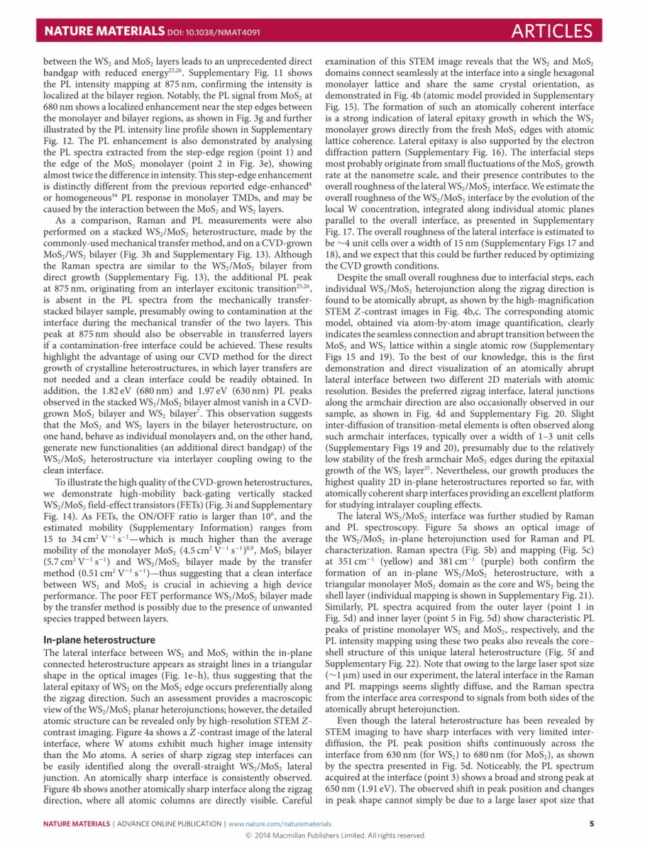
In-plane heterostructureThe lateral interface between WS2 and MoS2 within the in-planeconnected heterostructure appears as straight lines in a triangularshape in the optical images (Fig. 1e–h), thus suggesting that thelateral epitaxy of WS2 on the MoS2 edge occurs preferentially alongthe zigzag direction. Such an assessment provides a macroscopicview of theWS2/MoS2 planar heterojunctions; however, the detailedatomic structure can be revealed only by high-resolution STEM Z-contrast imaging. Figure 4a shows a Z-contrast image of the lateralinterface, where W atoms exhibit much higher image intensitythan the Mo atoms. A series of sharp zigzag step interfaces canbe easily identified along the overall-straight WS2/MoS2 lateraljunction. An atomically sharp interface is consistently observed.Figure 4b shows another atomically sharp interface along the zigzagdirection, where all atomic columns are directly visible. Careful
examination of this STEM image reveals that the WS2 and MoS2domains connect seamlessly at the interface into a single hexagonalmonolayer lattice and share the same crystal orientation, asdemonstrated in Fig. 4b (atomic model provided in SupplementaryFig. 15). The formation of such an atomically coherent interfaceis a strong indication of lateral epitaxy growth in which the WS2monolayer grows directly from the fresh MoS2 edges with atomiclattice coherence. Lateral epitaxy is also supported by the electrondiffraction pattern (Supplementary Fig. 16). The interfacial stepsmost probably originate from small fluctuations of theMoS2 growthrate at the nanometre scale, and their presence contributes to theoverall roughness of the lateralWS2/MoS2 interface.We estimate theoverall roughness of the WS2/MoS2 interface by the evolution of thelocal W concentration, integrated along individual atomic planesparallel to the overall interface, as presented in SupplementaryFig. 17. The overall roughness of the lateral interface is estimated tobe ∼4 unit cells over a width of 15 nm (Supplementary Figs 17 and18), and we expect that this could be further reduced by optimizingthe CVD growth conditions.
Despite the small overall roughness due to interfacial steps, eachindividual WS2/MoS2 heterojunction along the zigzag direction isfound to be atomically abrupt, as shown by the high-magnificationSTEM Z-contrast images in Fig. 4b,c. The corresponding atomicmodel, obtained via atom-by-atom image quantification, clearlyindicates the seamless connection and abrupt transition between theMoS2 and WS2 lattice within a single atomic row (SupplementaryFigs 15 and 19). To the best of our knowledge, this is the firstdemonstration and direct visualization of an atomically abruptlateral interface between two different 2D materials with atomicresolution. Besides the preferred zigzag interface, lateral junctionsalong the armchair direction are also occasionally observed in oursample, as shown in Fig. 4d and Supplementary Fig. 20. Slightinter-diffusion of transition-metal elements is often observed alongsuch armchair interfaces, typically over a width of 1–3 unit cells(Supplementary Figs 19 and 20), presumably due to the relativelylow stability of the fresh armchair MoS2 edges during the epitaxialgrowth of the WS2 layer35. Nevertheless, our growth produces thehighest quality 2D in-plane heterostructures reported so far, withatomically coherent sharp interfaces providing an excellent platformfor studying intralayer coupling effects.
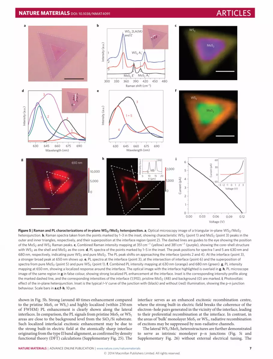
The lateral WS2/MoS2 interface was further studied by Ramanand PL spectroscopy. Figure 5a shows an optical image ofthe WS2/MoS2 in-plane heterojunction used for Raman and PLcharacterization. Raman spectra (Fig. 5b) and mapping (Fig. 5c)at 351 cm−1 (yellow) and 381 cm−1 (purple) both confirm theformation of an in-plane WS2/MoS2 heterostructure, with atriangular monolayer MoS2 domain as the core and WS2 being theshell layer (individual mapping is shown in Supplementary Fig. 21).Similarly, PL spectra acquired from the outer layer (point 1 inFig. 5d) and inner layer (point 5 in Fig. 5d) show characteristic PLpeaks of pristine monolayer WS2 and MoS2, respectively, and thePL intensity mapping using these two peaks also reveals the core–shell structure of this unique lateral heterostructure (Fig. 5f andSupplementary Fig. 22). Note that owing to the large laser spot size(∼1 µm) used in our experiment, the lateral interface in the Ramanand PL mappings seems slightly diffuse, and the Raman spectrafrom the interface area correspond to signals from both sides of theatomically abrupt heterojunction.
Even though the lateral heterostructure has been revealed bySTEM imaging to have sharp interfaces with very limited inter-diffusion, the PL peak position shifts continuously across theinterface from 630 nm (for WS2) to 680 nm (for MoS2), as shownby the spectra presented in Fig. 5d. Noticeably, the PL spectrumacquired at the interface (point 3) shows a broad and strong peak at650 nm (1.91 eV). The observed shift in peak position and changesin peak shape cannot simply be due to a large laser spot size that
NATURE MATERIALS | ADVANCE ONLINE PUBLICATION | www.nature.com/naturematerials 5© 2014 Macmillan Publishers Limited. All rights reserved.
ARTICLES NATUREMATERIALS DOI: 10.1038/NMAT4091
W Mo S2
c
d
b
a
Figure 4 | Atomic structure of the lateral heterojunctions between WS2 and MoS2 monolayers. a,b, Atomic-resolution Z-contrast STEM images of thein-plane interface between WS2 and MoS2 domains. A small roughness resulting from interfacial steps can be seen in a. The red dashed lines highlight theatomically sharp interface along the zigzag-edge direction. The orange and pink dashed lines in b depict the atomic planes along the armchair and zigzagdirections, respectively, indicating the WS2 and MoS2 domains share the same crystal orientation. c,d, Atomic-resolution Z-contrast images of theatomically sharp lateral interfaces along the zigzag (c) and armchair (d) directions. The atomic models on the right correspond to the structure in thehighlighted regions. Scale bars: a, 1 nm; b–d, 0.5 nm.
picks up averaged information from an ∼1 µm2 area, as illustratedby the distinct difference between the PL spectrum acquired atthe interface (point 3) and the superposition of spectra from pureMoS2 and pure WS2 (Fig. 5e). Furthermore, PL intensity mappingat 650 nm (Fig. 5g) reveals that this strong PL response is localizedat the lateral interface, and the intensity drops significantly at theintersections of these interfaces, which is consistent with the PLspectra presented in Fig. 5e. The shift of the PL peak to intermediateenergies near the interface can be explained as follows. Excitonsnear the interface have wavefunctions that overlap the other side,
which causes a shift that gradually evolves to the excitonic peakon the other side. When the laser spot is focused on the interface,it generates excitons at intermediate energies, resulting in theobserved broad peak between the two pristine excitonic peaks. Thisobserved peak contains contributions from excitons that have anelectron predominantly on one side and a hole predominantly onthe other side (such excitons also have an intermediate energy, asdiscussed in Supplementary Figs 23 and 24).
To further assess the localized interfacial effect, we acquired ahigh-resolution PL microscope image from the heterostructure, as
6 NATURE MATERIALS | ADVANCE ONLINE PUBLICATION | www.nature.com/naturematerials© 2014 Macmillan Publishers Limited. All rights reserved.
NATUREMATERIALS DOI: 10.1038/NMAT4091 ARTICLES
132
WS2
MoS2
WS2
MoS2
654 321
5
3
2
6
1 + 5
3
1 4
Inte
nsity
(a.u
.)
Inte
nsity
(a.u
.)
Inte
nsity
(a.u
.)
Inte
nsity
(a.u
.)
Raman shift (cm−1)
Wavelength (nm) Wavelength (nm)
X (µm)
MoS2 A1’MoS2 E’
1
WS2 2LA(M) and E’
WS2 A1’
2
3
50
48
1,910 60
30
−30−3 −2 0 1 2 3−1
Voltage (V)
Voltage (V)
01510 20
5,000 1,000
0
00.00 0.03 0.06 0.09 0.12
1
2
3
4
5
6
0
10,0002,000
650 nm
Curr
ent (
pA)
Curr
ent (
pA)
a
d
g h i
e f
b c
630 645 660 675 690
300 330 360 390 420 450 480
630 645 660 675 690
Figure 5 | Raman and PL characterizations of in-plane WS2/MoS2 heterojunction. a, Optical microscopy image of a triangular in-plane WS2/MoS2heterojunction. b, Raman spectra taken from the points marked by 1–3 in the inset, showing characteristic WS2 (point 1) and MoS2 (point 3) peaks in theouter and inner triangles, respectively, and their superposition at the interface region (point 2). The dashed lines are guides to the eye showing the positionof the MoS2 and WS2 Raman peaks. c, Combined Raman intensity mapping at 351 cm−1 (yellow) and 381 cm−1 (purple), showing the core–shell structurewith WS2 as the shell and MoS2 as the core. d, PL spectra of the points marked by 1–5 in the inset. The peak positions for spectra 1 and 5 are 630 nm and680 nm, respectively, indicating pure WS2 and pure MoS2. The PL peak shifts on approaching the interface (points 2 and 4). At the interface (point 3),a stronger broad peak at 650 nm shows up. e, PL spectra at the interface (point 3), at the intersection of interface (point 6) and the superposition ofspectra from pure MoS2 (point 5) and pure WS2 (point 1). f, Combined PL intensity mapping at 630 nm (orange) and 680 nm (green). g, PL intensitymapping at 650 nm, showing a localized response around the interface. The optical image with the interface highlighted is overlaid in g. h, PL microscopeimage of the same region in g in false colour, showing strong localized PL enhancement at the interface. Inset is the corresponding intensity profile alongthe marked dashed line, and the corresponding intensities of the interface (1,910), pristine MoS2 (48) and background (0) are marked. i, Photovoltaice�ect of the in-plane heterojunction. Inset is the typical I–V curve of the junction with (black) and without (red) illumination, showing the p–n junctionbehaviour. Scale bars in a,c,f–h, 10 µm.
shown in Fig. 5h. Strong (around 40 times enhancement comparedto the pristine MoS2 or WS2) and highly localized (within 250 nmof FWHM) PL enhancement is clearly shown along the lateralinterfaces. In comparison, the PL signals from pristineMoS2 orWS2areas are close to the background level from the SiO2/Si substrate.Such localized interfacial excitonic enhancement may be due tothe strong built-in electric field at the atomically sharp interfaceoriginating from the type II band alignment, as confirmedby densityfunctional theory (DFT) calculations (Supplementary Fig. 25). The
interface serves as an enhanced excitonic recombination centre,where the strong built-in electric field breaks the coherence of theelectron–hole pairs generated in the vicinity of the interface, leadingto their preferential recombination at the interface. In contrast, inthe areas of ‘bulk’ monolayer MoS2 orWS2, radiative recombinationof excitons may be suppressed by non-radiative channels.
The lateralWS2/MoS2 heterostructures are further demonstratedto serve as intrinsic monolayer p–n junctions (Fig. 5i andSupplementary Fig. 26) without external electrical tuning. The
NATURE MATERIALS | ADVANCE ONLINE PUBLICATION | www.nature.com/naturematerials 7© 2014 Macmillan Publishers Limited. All rights reserved.
ARTICLES NATUREMATERIALS DOI: 10.1038/NMAT4091
forward bias current is two orders of magnitude higher than thereverse current, implying a good rectification character, uniquein 2D electronics. Furthermore, under illumination, the lateralheterostructure shows a clear photovoltaic effect, which is alsosolid evidence for the existence of a p–n junction (Fig. 5i).Such a photovoltaic effect is consistent with the band alignmentcalculations presented in Supplementary Fig. 25. An open-loopvoltage of 0.12V and close-loop current of 5.7 pA is obtained. Thisis the first time that the p–n junction and photovoltaic effect havebeen achieved in monolayer materials without external gating15–17.
In summary, we have demonstrated the growth of high-qualityvertical and lateral WS2/MoS2 heterostructures with clean andatomically sharp interfaces. The well-defined, sharp and cleaninterfaces in these heterostructures allow us to explore new andcontrolled designs for 2D materials. The specific orientationrelationships and ordering between the individual monolayerdomains can lead to specific interface electronic properties thatcannot be obtained in randomly assembled van der Waalsheteromaterials. Such scalable methods to grow engineered 2Dheterostructures could lead to interesting applications, such asvertically stacked FET devices and planar monolayer devices.Combining both vertical and lateral 2D heterostructures opensup the possibility to create unprecedented architectures using 2Datomic layer building blocks.
Received 25 April 2014; accepted 20 August 2014;published online 28 September 2014
References1. Kroemer, H. Heterostructure bipolar transistors and integrated circuits. Proc.
IEEE 70, 13–25 (1982).2. Ohno, Y. et al. Electrical spin injection in a ferromagnetic semiconductor
heterostructure. Nature 402, 790–792 (1999).3. Novoselov, K. S. et al. Two-dimensional gas of massless Dirac fermions in
graphene. Nature 438, 197–200 (2005).4. Dean, C. R. et al. Boron nitride substrates for high-quality graphene
electronics. Nature Nanotech. 5, 722–726 (2010).5. Song, L. et al. Large scale growth and characterization of atomic hexagonal
boron nitride layers. Nano Lett. 10, 3209–3215 (2010).6. Gutierrez, H. R. et al. Extraordinary room-temperature photoluminescence in
triangular WS2 monolayers. Nano Lett. 13, 3447–3454 (2013).7. Mak, K. F., Lee, C., Hone, J., Shan, J. & Heinz, T. F. Atomically thin MoS2:
A new direct-gap semiconductor. Phys. Rev. Lett. 105, 136805 (2010).8. Najmaei, S. et al. Vapour phase growth and grain boundary structure of
molybdenum disulphide atomic layers. Nature Mater. 12, 754–759 (2013).9. van der Zande, A. M. et al. Grains and grain boundaries in highly crystalline
monolayer molybdenum disulphide. Nature Mater. 12, 554–561 (2013).10. Britnell, L. et al. Field-effect tunneling transistor based on vertical graphene
heterostructures. Science 335, 947–950 (2012).11. Gannett, W. et al. Boron nitride substrates for high mobility chemical vapor
deposited graphene. Appl. Phys. Lett. 98, 242105 (2011).12. Geim, A. K. & Grigorieva, I. V. Van der Waals heterostructures. Nature 499,
419–425 (2013).13. Georgiou, T. et al. Vertical field-effect transistor based on graphene-WS2
heterostructures for flexible and transparent electronics. Nature Nanotech. 8,100–103 (2013).
14. Yu, W. J. et al.Highly efficient gate-tunable photocurrent generation in verticalheterostructures of layered materials. Nature Nanotech. 8, 952–958 (2013).
15. Pospischil, A., Furchi, M. M. & Mueller, T. Solar-energy conversion andlight emission in an atomic monolayer p–n diode. Nature Nanotech. 9,257–261 (2014).
16. Baugher, B. W., Churchill, H. O., Yang, Y. & Jarillo-Herrero, P. Optoelectronicdevices based on electrically tunable p–n diodes in a monolayerdichalcogenide. Nature Nanotech. 9, 262–267 (2014).
17. Ross, J. S. et al. Electrically tunable excitonic light-emitting diodes based onmonolayer WSe2 p–n junctions. Nature Nanotech. 9, 268–272 (2014).
18. Haigh, S. J. et al. Cross-sectional imaging of individual layers and buriedinterfaces of graphene-based heterostructures and superlattices. Nature Mater.11, 764–767 (2012).
19. Yang, W. et al. Epitaxial growth of single-domain graphene on hexagonal boronnitride. Nature Mater. 12, 792–797 (2013).
20. Levendorf, M. P. et al. Graphene and boron nitride lateral heterostructures foratomically thin circuitry. Nature 488, 627–632 (2012).
21. Liu, Z. et al. In-plane heterostructures of graphene and hexagonal boron nitridewith controlled domain sizes. Nature Nanotech. 8, 119–124 (2013).
22. Liu, L. et al.Heteroepitaxial growth of two-dimensional hexagonal boronnitride templated by graphene edges. Science 343, 163–167 (2014).
23. Han, G. H. et al. Continuous growth of hexagonal graphene and boron nitridein-plane heterostructures by atmospheric pressure chemical vapor deposition.ACS Nano 7, 10129–10138 (2013).
24. Miyata, Y. et al. Fabrication and characterization of graphene/hexagonal boronnitride hybrid sheets. Appl. Phys. Express 5, 085102 (2012).
25. Kosmider, K. & Fernandez-Rossier, J. Electronic properties of the MoS2–WS2heterojunction. Phys. Rev. B 87, 075451 (2013).
26. Terrones, H., Lopez-Urias, F. & Terrones, M. Novel hetero-layered materialswith tunable direct band gaps by sandwiching different metal disulfides anddiselenides. Sci. Rep. 3, 1549 (2013).
27. Kang, J., Tongay, S., Zhou, J., Li, J. B. & Wu, J. Q. Band offsets andheterostructures of two-dimensional semiconductors. Appl. Phys. Lett. 102,012111 (2013).
28. Krivanek, O. L. et al. Atom-by-atom structural and chemical analysis byannular dark-field electron microscopy. Nature 464, 571–574 (2010).
29. Zhou, W. et al. Intrinsic structural defects in monolayer molybdenum disulfide.Nano Lett. 13, 2615–2622 (2013).
30. Gong, Y. J. et al. Band gap engineering and layer-by-layer mapping ofselenium-doped molybdenum disulfide. Nano Lett. 14, 442–449 (2014).
31. Terrones, H. et al. New first order Raman-active modes in few layeredtransition metal dichalcogenides. Sci. Rep. 4, 4215 (2014).
32. Berkdemir, A. et al. Identification of individual and few layers of WS2 usingRaman spectroscopy. Sci. Rep. 3, 1755 (2013).
33. Zhao, W. J. et al. Evolution of electronic structure in atomically thin sheets ofWS2 and WSe2. ACS Nano 7, 791–797 (2013).
34. Peimyoo, N. et al. Nonblinking, intense two-dimensional light emitter:Monolayer WS2 triangles. ACS Nano 7, 10985–10994 (2013).
35. Wang, Z. et al.Mixed low-dimensional nanomaterial: 2D ultranarrow MoS2inorganic nanoribbons encapsulated in quasi-1D carbon nanotubes. J. Am.Chem. Soc. 132, 13840–13847 (2010).
AcknowledgementsWe thank A. Lupini for providing the script for STEM image quantification. This workwas supported by the Army Research Office MURI grant W911NF-11-1-0362, US DOEgrant DE-FG02-09ER46554 (J.L., S.T.P.), a Wigner Fellowship through the LaboratoryDirected Research and Development Program of Oak Ridge National Laboratory(ORNL), managed by UT-Battelle, LLC, for the US DOE (W.Z.), the FAME Center, one ofsix centres of STARnet, a Semiconductor Research Corporation program sponsored byMARCO and DARPA, the US Office of Naval Research MURI grant N000014-09-1-1066,NSF grant ECCS-1327093 and MOE Academic Research Fund (AcRF) Tier 1 RG81/12project Singapore and Si-COE project, Singapore. This research was also supportedthrough a user project supported by ORNL’s Center for Nanophase Materials Sciences(CNMS), which is sponsored by the Scientific User Facilities Division, Office of BasicEnergy Sciences, US DOE. This research used resources of the National Energy ResearchScientific Computing Center, which is supported by the Office of Science of the USDepartment of Energy under Contract No. DE-AC02-05CH11231. This work was alsosupported by the Singapore National Research Foundation under NRF RF AwardNo. NRF-RF2013-08, the start-up funding from Nanyang Technological University(M4081137.070).
Author contributionsY.G., J.L. and X.W. contributed equally to this work. Y.G. designed the growth proceduresand carried out part of the characterization. Y.G., X.W. and G.Y. worked on the growth.W.Z. and J.L. carried out STEM experiments. G.S. and S.L. made the FET devices andcarried out the electrical measurement. Z.L. performed part of the Raman and PLcharacterization. H.T., X.Z. and J.L. carried out DFT calculations. Y.G., J.L., X.W., W.Z.,Z.L., G.S., S.L., M.T., H.T. and P.M.A. analysed the results and co-wrote the paper. Allauthors participated in discussions.
Additional informationSupplementary information is available in the online version of the paper. Reprints andpermissions information is available online at www.nature.com/reprints.Correspondence and requests for materials should be addressed to W.Z. or P.M.A.
Competing financial interestsThe authors declare no competing financial interests.
8 NATURE MATERIALS | ADVANCE ONLINE PUBLICATION | www.nature.com/naturematerials© 2014 Macmillan Publishers Limited. All rights reserved.
Related Documents