Vector Processing as a Soft-CPU Accelerator by Jason Kwok Kwun Yu B.A.Sc, Simon Fraser University, 2005 A THESIS SUBMITTED IN PARTIAL FULFILMENT OF THE REQUIREMENTS FOR THE DEGREE OF Master of Applied Science in The Faculty of Graduate Studies (Electrical and Computer Engineering) The University Of British Columbia May, 2008 c Jason Kwok Kwun Yu 2008

Welcome message from author
This document is posted to help you gain knowledge. Please leave a comment to let me know what you think about it! Share it to your friends and learn new things together.
Transcript
Vector Processing as a Soft-CPUAccelerator
by
Jason Kwok Kwun Yu
B.A.Sc, Simon Fraser University, 2005
A THESIS SUBMITTED IN PARTIAL FULFILMENT OFTHE REQUIREMENTS FOR THE DEGREE OF
Master of Applied Science
in
The Faculty of Graduate Studies
(Electrical and Computer Engineering)
The University Of British Columbia
May, 2008
c© Jason Kwok Kwun Yu 2008

ii

Abstract
Soft processors simplify hardware design by being able to implement complex control strate-
gies using software. However, they are not fast enough for many intensive data-processing
tasks, such as highly data-parallel embedded applications. This thesis suggests adding a vector
processing core to the soft processor as a general-purpose accelerator for these types of applica-
tions. The approach has the benefits of a purely software-oriented development model, a fixed
ISA allowing parallel software and hardware development, a single accelerator that can accel-
erate multiple functions in an application, and scalable performance with a single source code.
With no hardware design experience needed, a software programmer can make area-versus-
performance tradeoffs by scaling the number of functional units and register file bandwidth
with a single parameter. The soft vector processor can be further customized by a number
of secondary parameters to add and remove features for the specific application to optimize
resource utilization. This thesis shows that a vector processing architecture maps efficiently
into an FPGA and provides a scalable amount of performance for a reasonable amount of area.
Configurations of the soft vector processor with different performance levels are estimated to
achieve speedups of 2–24× for 5–26× the area of a Nios II/s processor on three benchmark
kernels.
iii

Abstract
iv

Table of Contents
Abstract . . . . . . . . . . . . . . . . . . . . . . . . . . . . . . . . . . . . . . . . . . . . iii
Table of Contents . . . . . . . . . . . . . . . . . . . . . . . . . . . . . . . . . . . . . . . v
List of Tables . . . . . . . . . . . . . . . . . . . . . . . . . . . . . . . . . . . . . . . . . xi
List of Figures . . . . . . . . . . . . . . . . . . . . . . . . . . . . . . . . . . . . . . . . . xiii
Acknowledgments . . . . . . . . . . . . . . . . . . . . . . . . . . . . . . . . . . . . . . xv
1 Introduction . . . . . . . . . . . . . . . . . . . . . . . . . . . . . . . . . . . . . . . . 1
1.1 Motivation . . . . . . . . . . . . . . . . . . . . . . . . . . . . . . . . . . . . . . . 3
1.2 Contributions . . . . . . . . . . . . . . . . . . . . . . . . . . . . . . . . . . . . . 5
1.3 Thesis Outline . . . . . . . . . . . . . . . . . . . . . . . . . . . . . . . . . . . . . 6
2 Background . . . . . . . . . . . . . . . . . . . . . . . . . . . . . . . . . . . . . . . . 7
2.1 Vector Processing Overview . . . . . . . . . . . . . . . . . . . . . . . . . . . . . 7
2.1.1 Exploiting Data-level Parallelism . . . . . . . . . . . . . . . . . . . . . . 8
2.1.2 Vector Instruction Set Architecture . . . . . . . . . . . . . . . . . . . . . 10
2.1.3 Microarchitectural Advantages of Vector Processing . . . . . . . . . . . . 11
2.2 Vector Processors and SIMD Extensions . . . . . . . . . . . . . . . . . . . . . . 12
2.2.1 SIMD Extensions . . . . . . . . . . . . . . . . . . . . . . . . . . . . . . . 12
2.2.2 Single-chip Vector Processors . . . . . . . . . . . . . . . . . . . . . . . . . 13
v
Table of Contents
2.2.3 FPGA-based Vector Processors . . . . . . . . . . . . . . . . . . . . . . . 13
2.3 Multiprocessor Systems . . . . . . . . . . . . . . . . . . . . . . . . . . . . . . . . 15
2.4 Custom-designed Hardware Accelerators . . . . . . . . . . . . . . . . . . . . . . 17
2.4.1 Decoupled Co-processor Accelerators . . . . . . . . . . . . . . . . . . . . 17
2.4.2 Custom Instruction Accelerators . . . . . . . . . . . . . . . . . . . . . . . 18
2.5 Synthesized Hardware Accelerators . . . . . . . . . . . . . . . . . . . . . . . . . 20
2.5.1 C-based Synthesis . . . . . . . . . . . . . . . . . . . . . . . . . . . . . . . 20
2.5.2 Block-based Synthesis . . . . . . . . . . . . . . . . . . . . . . . . . . . . . 24
2.5.3 Application Specific Instruction Set Processor . . . . . . . . . . . . . . . 26
2.5.4 Synthesis from Binary Decompilation . . . . . . . . . . . . . . . . . . . . 27
2.6 Other Soft Processor Architectures . . . . . . . . . . . . . . . . . . . . . . . . . 28
2.6.1 Mitrion Virtual Processor . . . . . . . . . . . . . . . . . . . . . . . . . . . 28
2.6.2 VLIW Processors . . . . . . . . . . . . . . . . . . . . . . . . . . . . . . . 29
2.6.3 Superscalar Processors . . . . . . . . . . . . . . . . . . . . . . . . . . . . 30
2.7 Summary . . . . . . . . . . . . . . . . . . . . . . . . . . . . . . . . . . . . . . . . 31
3 Configurable Soft Vector Processor . . . . . . . . . . . . . . . . . . . . . . . . . 33
3.1 Requirements . . . . . . . . . . . . . . . . . . . . . . . . . . . . . . . . . . . . . . 33
3.2 Soft Vector Architecture . . . . . . . . . . . . . . . . . . . . . . . . . . . . . . . 34
3.2.1 System Overview . . . . . . . . . . . . . . . . . . . . . . . . . . . . . . . 34
3.2.2 Hybrid Vector-SIMD Model . . . . . . . . . . . . . . . . . . . . . . . . . 36
3.3 Vector Lane Datapath . . . . . . . . . . . . . . . . . . . . . . . . . . . . . . . . . 37
3.3.1 Vector Pipeline . . . . . . . . . . . . . . . . . . . . . . . . . . . . . . . . 37
3.3.2 Datapath Functional Units . . . . . . . . . . . . . . . . . . . . . . . . . . 39
3.3.3 Distributed Vector Register File . . . . . . . . . . . . . . . . . . . . . . . 40
3.3.4 Load Store Unit . . . . . . . . . . . . . . . . . . . . . . . . . . . . . . . . 40
3.3.5 Local Memory . . . . . . . . . . . . . . . . . . . . . . . . . . . . . . . . . 41
vi

3.4 Memory Unit . . . . . . . . . . . . . . . . . . . . . . . . . . . . . . . . . . . . . . 41
3.4.1 Load Store Controller . . . . . . . . . . . . . . . . . . . . . . . . . . . . . 42
3.4.2 Read Interface . . . . . . . . . . . . . . . . . . . . . . . . . . . . . . . . . 42
3.4.3 Write Interface . . . . . . . . . . . . . . . . . . . . . . . . . . . . . . . . . 43
3.5 FPGA-Specific Vector Extensions . . . . . . . . . . . . . . . . . . . . . . . . . . 45
3.6 Configurable Parameters . . . . . . . . . . . . . . . . . . . . . . . . . . . . . . . 47
3.7 Design Flow . . . . . . . . . . . . . . . . . . . . . . . . . . . . . . . . . . . . . . 48
3.7.1 Soft Vector Processor Flow versus C-based Synthesis . . . . . . . . . . . 48
3.7.2 Comment on Vectorizing Compilers . . . . . . . . . . . . . . . . . . . . . 50
4 Results . . . . . . . . . . . . . . . . . . . . . . . . . . . . . . . . . . . . . . . . . . . 51
4.1 Benchmark Suite . . . . . . . . . . . . . . . . . . . . . . . . . . . . . . . . . . . . 51
4.2 Benchmark Preparation . . . . . . . . . . . . . . . . . . . . . . . . . . . . . . . . 53
4.2.1 General Methodology . . . . . . . . . . . . . . . . . . . . . . . . . . . . . 54
4.2.2 Benchmark Vectorization . . . . . . . . . . . . . . . . . . . . . . . . . . . 54
4.2.3 Benchmark Tuning for C2H Compiler . . . . . . . . . . . . . . . . . . . . 59
4.2.4 Soft Vector Processor Per Benchmark Configuration . . . . . . . . . . . . 60
4.3 Resource Utilization Results . . . . . . . . . . . . . . . . . . . . . . . . . . . . . 60
4.4 Performance Results . . . . . . . . . . . . . . . . . . . . . . . . . . . . . . . . . . 63
4.4.1 Performance Models . . . . . . . . . . . . . . . . . . . . . . . . . . . . . . 64
4.4.2 RTL Model Performance . . . . . . . . . . . . . . . . . . . . . . . . . . . 66
4.4.3 Ideal Vector Model . . . . . . . . . . . . . . . . . . . . . . . . . . . . . . 68
4.4.4 C2H Accelerator Results . . . . . . . . . . . . . . . . . . . . . . . . . . . 70
4.4.5 Vector versus C2H . . . . . . . . . . . . . . . . . . . . . . . . . . . . . . . 71
5 Conclusions and Future Work . . . . . . . . . . . . . . . . . . . . . . . . . . . . . 73
5.1 Future Work . . . . . . . . . . . . . . . . . . . . . . . . . . . . . . . . . . . . . . 75
vii
Table of Contents
Bibliography . . . . . . . . . . . . . . . . . . . . . . . . . . . . . . . . . . . . . . . . . . 79
Appendices
A Soft Vector Processor ISA . . . . . . . . . . . . . . . . . . . . . . . . . . . . . . . 85
A.1 Introduction . . . . . . . . . . . . . . . . . . . . . . . . . . . . . . . . . . . . . . 85
A.1.1 Configurable Architecture . . . . . . . . . . . . . . . . . . . . . . . . . . 86
A.1.2 Memory Consistency . . . . . . . . . . . . . . . . . . . . . . . . . . . . . 87
A.2 Vector Register Set . . . . . . . . . . . . . . . . . . . . . . . . . . . . . . . . . . 87
A.2.1 Vector Registers . . . . . . . . . . . . . . . . . . . . . . . . . . . . . . . . 87
A.2.2 Vector Scalar Registers . . . . . . . . . . . . . . . . . . . . . . . . . . . . 88
A.2.3 Vector Flag Registers . . . . . . . . . . . . . . . . . . . . . . . . . . . . . 88
A.2.4 Vector Control Registers . . . . . . . . . . . . . . . . . . . . . . . . . . . 89
A.2.5 Multiply-Accumulators for Vector Sum Reduction . . . . . . . . . . . . . 90
A.2.6 Vector Lane Local Memory . . . . . . . . . . . . . . . . . . . . . . . . . . 90
A.3 Instruction Set . . . . . . . . . . . . . . . . . . . . . . . . . . . . . . . . . . . . . 92
A.3.1 Data Types . . . . . . . . . . . . . . . . . . . . . . . . . . . . . . . . . . 92
A.3.2 Addressing Modes . . . . . . . . . . . . . . . . . . . . . . . . . . . . . . . 92
A.3.3 Flag Register Use . . . . . . . . . . . . . . . . . . . . . . . . . . . . . . . 92
A.3.4 Instructions . . . . . . . . . . . . . . . . . . . . . . . . . . . . . . . . . . 92
A.4 Instruction Set Reference . . . . . . . . . . . . . . . . . . . . . . . . . . . . . . . 93
A.4.1 Integer Instructions . . . . . . . . . . . . . . . . . . . . . . . . . . . . . . 93
A.4.2 Logical Instructions . . . . . . . . . . . . . . . . . . . . . . . . . . . . . . 96
A.4.3 Fixed-Point Instructions (Future Extension) . . . . . . . . . . . . . . . . 96
A.4.4 Memory Instructions . . . . . . . . . . . . . . . . . . . . . . . . . . . . . 99
A.4.5 Vector Processing Instructions . . . . . . . . . . . . . . . . . . . . . . . . 102
A.4.6 Vector Flag Processing Instructions . . . . . . . . . . . . . . . . . . . . . 105
viii

A.4.7 Miscellaneous Instructions . . . . . . . . . . . . . . . . . . . . . . . . . . 106
A.5 Instruction Formats . . . . . . . . . . . . . . . . . . . . . . . . . . . . . . . . . . 107
A.5.1 Vector Register and Vector Scalar Instructions . . . . . . . . . . . . . . . 107
A.5.2 Vector Memory Instructions . . . . . . . . . . . . . . . . . . . . . . . . . 108
A.5.3 Instruction Encoding . . . . . . . . . . . . . . . . . . . . . . . . . . . . . 109
ix

Table of Contents
x
List of Tables
1.1 New soft vector processor instruction extensions . . . . . . . . . . . . . . . . . . 6
2.1 Partial list of FPGA-based multiprocessor systems in literature . . . . . . . . . . 17
3.1 List of configurable processor parameters . . . . . . . . . . . . . . . . . . . . . . 48
4.1 Per benchmark soft vector processor configuration parameter settings . . . . . . 60
4.2 Resource usage of vector processor and C2H accelerator configurations . . . . . . 61
4.3 Resource usage of vector processor when varying NLane and MemMinWidth with
128-bit MemWidth and otherwise full features . . . . . . . . . . . . . . . . . . . . 62
4.4 Resource utilization from varying secondary processor parameters . . . . . . . . . 63
4.5 Ideal vector performance model . . . . . . . . . . . . . . . . . . . . . . . . . . . . 65
4.6 Performance measurements . . . . . . . . . . . . . . . . . . . . . . . . . . . . . . 67
A.1 List of configurable processor parameters . . . . . . . . . . . . . . . . . . . . . . 87
A.2 List of vector flag registers . . . . . . . . . . . . . . . . . . . . . . . . . . . . . . . 88
A.3 List of control registers . . . . . . . . . . . . . . . . . . . . . . . . . . . . . . . . . 89
A.4 Instruction qualifiers . . . . . . . . . . . . . . . . . . . . . . . . . . . . . . . . . . 93
A.11 Nios II Opcode Usage . . . . . . . . . . . . . . . . . . . . . . . . . . . . . . . . . 107
A.12 Scalar register usage as source or destination register . . . . . . . . . . . . . . . . 108
A.13 Vector register instruction function field encoding (OPX=0) . . . . . . . . . . . . 109
A.14 Scalar-vector instruction function field encoding (OPX=1) . . . . . . . . . . . . . 110
A.15 Fixed-point instruction function field encoding (OPX=0) . . . . . . . . . . . . . 110
xi

List of Tables
A.16 Flag and miscellaneous instruction function field encoding (OPX=1) . . . . . . . 111
A.17 Memory instruction function field encoding . . . . . . . . . . . . . . . . . . . . . 111
xii
List of Figures
2.1 8-tap FIR filter MIPS assembly . . . . . . . . . . . . . . . . . . . . . . . . . . . . 9
2.2 8-tap FIR filter VIRAM vector assembly . . . . . . . . . . . . . . . . . . . . . . . 10
2.3 Nios II custom instruction formats . . . . . . . . . . . . . . . . . . . . . . . . . . 19
2.4 Example Nios II system with C2H accelerators. . . . . . . . . . . . . . . . . . . . 22
3.1 Scalar and vector core interaction . . . . . . . . . . . . . . . . . . . . . . . . . . . 35
3.2 Vector chaining versus hybrid vector-SIMD execution . . . . . . . . . . . . . . . . 36
3.3 Vector co-processor system block diagram . . . . . . . . . . . . . . . . . . . . . . 38
3.4 Vector Lane ALU . . . . . . . . . . . . . . . . . . . . . . . . . . . . . . . . . . . . 39
3.5 Soft vector processor write interface. . . . . . . . . . . . . . . . . . . . . . . . . . 43
3.6 Data alignment using crossbar and delay network for vector store. . . . . . . . . 44
3.7 8-tap FIR filter vector assembly . . . . . . . . . . . . . . . . . . . . . . . . . . . . 47
3.8 Altera C2H compiler design flow versus soft vector processor design flow . . . . . 49
4.1 Motion estimation C code . . . . . . . . . . . . . . . . . . . . . . . . . . . . . . . 52
4.2 5 × 5 median filter C code . . . . . . . . . . . . . . . . . . . . . . . . . . . . . . . 53
4.3 Simultaneously matching two copies of the macroblock to a reference frame . . . 55
4.4 Code segment from the motion estimation vector assembly. The code to handle
the first and last rows of the windows are not shown. . . . . . . . . . . . . . . . . 56
4.5 Vectorizing the image median filter . . . . . . . . . . . . . . . . . . . . . . . . . . 57
4.6 Median filter inner loop vector assembly . . . . . . . . . . . . . . . . . . . . . . . 57
4.7 Vector assembly for loading AES data and performing AES encryption round . . 58
xiii

List of Figures
4.8 RTL Model speedup over Ideal Nios Model . . . . . . . . . . . . . . . . . . . . . 68
4.9 Ideal Vector Model and C2H Model speedup over Ideal Nios Model . . . . . . . . 69
A.1 Connection between distributed MAC units and the vector register file . . . . . . 91
xiv

Acknowledgments
Foremost I would like to thank my supervisor Dr. Guy Lemieux for teaching me the many as-
pects of academic research, and for his guidance and support throughout my research project.
The many hours you spent proofreading my conference papers and thesis are very much appre-
ciated.
Thanks to Blair Fort for providing the UTIIe processor used in this research, without which
this project would have taken much longer.
I would like to thank my friends in the SoC lab and throughout the department, on the
ECEGSA executive, and in the faculty music group for making my graduate life at UBC
enjoyable, and allowing me to develop both academically and personally during my life at
UBC.
Finally, I would like to thank my loving family and dear Florence for their constant support
and encouragement.
xv

Acknowledgments
xvi
Chapter 1
Introduction
Advanced signal processing algorithms and large volumes of multimedia data in many embed-
ded applications today demand high performance embedded systems. These systems rely on
programmable microprocessors, digital signal processors (DSPs), or field-programmable gate ar-
rays (FPGAs) to do intensive computations. Designing embedded systems using these platforms
requires expertise in both hardware and software, and is increasingly becoming a challenge due
to increasing complexity and performance requirements of today’s applications. A high perfor-
mance platform that is also easy to use and reduces time to market is needed to address these
challenges, and an effective FPGA-based soft processor platform is one possible solution.
FPGAs are a specialized type of integrated circuit (IC) that can be programmed and re-
programmed by the user after fabrication to implement any digital circuit. FPGAs achieve
this reconfigurability through the use of flexible lookup tables and routing connections that
are configured by a user-downloaded bitstream. There are a number of advantages to using
FPGAs in embedded systems. Manufacturing a set of masks to fabricate application specific
integrated circuits (ASICs) such as most microprocessors and DSPs costs millions of dollars in
today’s advanced fabrication technologies. The design, fabrication, and validation steps needed
to produce an ASIC is a lengthy process with a long turnaround time, and mistakes found
after fabrication require a new set of masks to correct and are thus very costly. These high
non-recurring engineering costs (NRE) make ASICs only practical for devices with sufficiently
large market and volume. FPGAs, on the other hand, can be purchased off the shelf with a
low up-front cost. The devices have been pre-tested by the FPGA vendor and are guaranteed
to function correctly. The reconfigurable nature allows users to quickly iterate their designs
1
Chapter 1. Introduction
during development, speeding up time to market. Even in the final product, reconfigurability
can allow the system firmware to be updated to take advantage of new firmware features or to
adhere to new standards. A single FPGA can also replace multiple components in a system
that would have required separate ICs, again reducing cost.
From a performance perspective, FPGAs are generally considered lower performance than
ASICs due to a lower maximum clock speed. Nonetheless, FPGAs are capable of tremendous
raw processing power. The reconfigurable lookup tables of an FPGA form one large compu-
tational fabric that is able to perform many operations in parallel, and the large number of
embedded on-chip memories can provide tremendous on-chip memory bandwidth. Consider the
largest Altera Stratix III FPGA, EP3SL340, which has approximately 135,000 adaptive logic
modules (ALMs). Each ALM is able to compute a one-bit function of up to six inputs per clock
cycle or implement up to two three-bit adders [1]. Taking the adders alone, if they can be fully
utilized, is equivalent to almost 8,440 three-input 32-bit adders. In comparison, many low-cost
microprocessors in embedded systems have only one two-input adder in a single arithmetic logic
unit (ALU).
Using FPGAs has traditionally required specialized hardware design knowledge and fa-
miliarity with a hardware description language (HDL) such as the VHSIC (Very High Speed
Integrated Circuit) Hardware Description Language (VHDL) or Verilog in order to implement
the desired circuitry. The introduction of embedded processor cores into FPGAs, both as hard
cores that are implemented in silicon like the rest of the FPGA circuitry, and as soft cores
that are synthesized and then programmed on to the FPGA like other user designs, has sim-
plified the design process and technical requirement of using FPGAs. According to a survey
conducted in 2007 [2], 36% of respondants used a processor (either hard or soft core) inside the
FPGA in their embedded designs, and this figure had increased from 33% in 2006, and 32% in
2005. Embedded software developers can now program in a high-level language such as C or
C++, and compile their programs to run on the embedded processor core within the FPGA.
This combination of embedded processor core and programmable logic has also opened up the
2
possibility of implementing custom hardware circuitry in the programmable logic to interact
with the processor core.
1.1 Motivation
More and more embedded systems today target multimedia, signal processing, and other com-
putationally intensive workloads. These applications typically have a relatively small set of
operations that have to be repeatedly performed over a large volume of data. This form of
parallelism is referred to as data-level parallelism. Current soft processors designed for FPGAs
such as Nios II [3] by Altera and MicroBlaze [4] by Xilinx frequently do not deliver enough com-
putational power to achieve the desired performance in these workloads. These soft processors
have only a single ALU and can only perform one computation per clock cycle. Although they
come in a few performance levels that successively add more advanced and complex architec-
tural features, even the highest performing core is frequently insufficient to handle the intensive
processing tasks.
Many solutions have been proposed in both commercial and academic spaces to improve the
performance of soft core processors on FPGAs. They can be largely categorized into four cat-
egories: multiprocessor systems, custom-designed hardware accelerators, synthesized hardware
accelerators, and other soft processor architectures. Multiprocessor systems contain multiple
processor cores, and rely upon shared memory or message passing to communicate and synchro-
nize. They generally require parallel programming knowledge from the user, and as a result are
more difficult to program and use. Hardware accelerators utilize the programmable logic of an
FPGA to implement dedicated accelerators for processing certain functions. Custom-designed
hardware accelerators have to be designed by the user in HDL, but the FPGA development
tools may provide an automated way to connect the accelerator to the processor core once it
has been designed. They still require the user to design hardware, and verify and test the
accelerator in hardware to ensure correct operation. Synthesized hardware accelerators are
3
Chapter 1. Introduction
automatically synthesized from a high-level language description or from a visual representa-
tion of the function to be accelerated. The major improvement is that users can use hardware
accelerators without knowledge of an HDL, and with little or no knowledge of hardware design.
An improved soft processor architecture has the benefit of a purely software solution, re-
quiring no hardware design or synthesis effort from the user. Depending on the complexity
of the programming model of the architecture, it can allow users to improve performance of
their applications with minimal learning curve. A soft processor also provides a specification
across hardware and software (in the form of a fixed instruction set architecture) that does not
change throughout the design cycle, allowing hardware and software development to proceed
in parallel.
Some common processor architectures have already been implemented in FPGAs. Very Long
Instruction Word (VLIW) architectures have been proposed for soft processors on FPGAs, and
superscalar architectures have also been attempted, but neither of them map efficiently to
the FPGA architecture, bloating resource usage and introducing unnecessary bottlenecks in
performance. To improve performance of data-parallel embedded applications on soft processor
systems, it is imperative to take advantage of the parallelism in the hardware. Given the pure
software advantage of using an improved soft processor architecture, an ideal solution would be
a processor architecture that is inherently parallel, and maps well to the FPGA architecture.
The solution proposed by this thesis is a soft processor tailored to FPGAs based on a
vector processor architecture. A vector processor is capable of high performance in data-
parallel embedded workloads. Kozyrakis [5] studied the vectorizability of the 10 consumer
and telecommunications benchmarks in the EEMBC suite using the VIRAM [6] compiler, and
found the average vector length of the benchmarks ranged from 13 to 128 (128 is the maximum
vector length supported by VIRAM). The study shows that many embedded applications are
vectorizable to long vector lengths, allowing significant performance improvements using vector
processing. Vector processing also satisfies the requirements of a parallel architecture, and can
be implemented efficiently in FPGAs, as will be shown in this thesis.
4
1.2 Contributions
The main contribution of this research is applying vector processing, an inherently parallel
programming model, to the architecture of soft core processors to improve their performance
on data-parallel embedded applications. A soft vector processor provides scalable and user-
selectable amount of acceleration and resource usage, and a configurable feature set, in a single
application-independent accelerator that requires zero hardware design knowledge or effort from
the user. The scalability of vector processoring allows users to make large performance and
resource tradeoffs in the vector processor with little or no modification to software. A soft
vector processor can further exploit the configurability of FPGAs by customizing the feature
set and instruction support of the processor to the target application. Customization extends
even to a configurable vector memory interface that can implement a memory system tailored to
the application. This makes accessible to the user a much larger design space and larger possible
tradeoffs than current soft processor solutions. The application-independent architecture of the
vector processor allows a single accelerator to accelerate multiple sections of an application and
multiple applications.
As part of this research, a complete soft vector processor was implemented in Verilog tar-
getting an Altera Stratix III FPGA to illustrate the feasibility of the approach and possible
performance gains. The processor adopts the VIRAM instruction set architecture (ISA), but
makes modifications to tailor the ISA features to FPGAs. A novel instruction execution model
that is a hybrid between traditional vector and single-instruction-multiple-data (SIMD) is used
in the processor. This work also identifies three ways traditional vector processor architectures
can be adapted to better exploit features of FPGAs:
1. Use of a partitioned register file to scale bandwidth and reduce complexity,
2. Use of multiply-accumulate (MAC) units for vector reduction,
3. Use of a local memory in each vector lane for lookup-table functions.
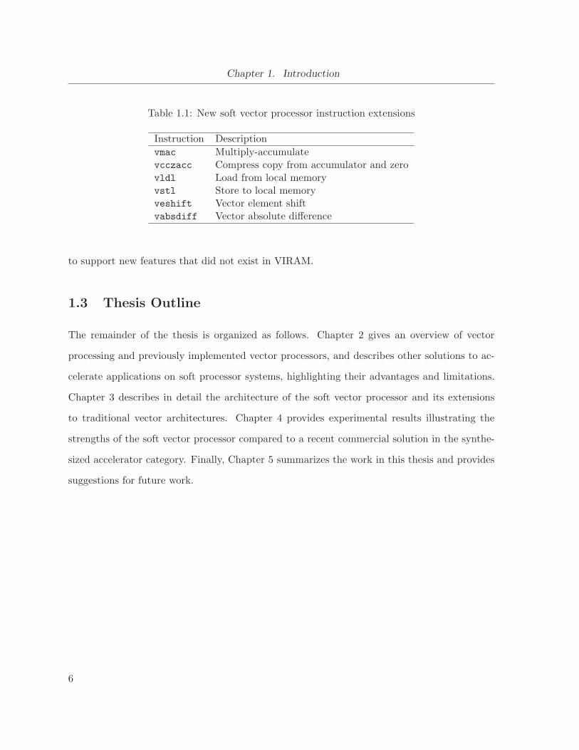
Table 1.1 lists new instructions that are added to the soft vector processor instruction set
5
Chapter 1. Introduction
Table 1.1: New soft vector processor instruction extensions
Instruction Description
vmac Multiply-accumulatevcczacc Compress copy from accumulator and zerovldl Load from local memoryvstl Store to local memoryveshift Vector element shiftvabsdiff Vector absolute difference
to support new features that did not exist in VIRAM.
1.3 Thesis Outline
The remainder of the thesis is organized as follows. Chapter 2 gives an overview of vector
processing and previously implemented vector processors, and describes other solutions to ac-
celerate applications on soft processor systems, highlighting their advantages and limitations.
Chapter 3 describes in detail the architecture of the soft vector processor and its extensions
to traditional vector architectures. Chapter 4 provides experimental results illustrating the
strengths of the soft vector processor compared to a recent commercial solution in the synthe-
sized accelerator category. Finally, Chapter 5 summarizes the work in this thesis and provides
suggestions for future work.
6
Chapter 2
Background
This chapter provides background on vector processing and application acceleration for soft
processor-based systems in FPGAs. First, an overview of how vector processing accelerates
data-parallel computations is presented, followed by a discussion of previously implemented
vector processors. The remainder of the chapter surveys other current solutions for improving
the performance of soft processors and accelerating FPGA-based applications. A representative
set of academic and commercial tools are described according to the four categories introduced
in Chapter 1: multiprocessor systems, custom-designed hardware accelerators, synthesized ac-
celerators, and other soft processor architectures.
2.1 Vector Processing Overview
Vector processing has been in use in supercomputers for scientific tasks for over two decades.
As semiconductor technology improved, single-chip vector processors have become possible, and
recent supercomputing systems like the Earth Simulator [7] and Cray X1 are based on such
single-chip vector processors. The next sections will give an overview of how vector processing
can accelerate data-parallel computations, and the characteristics of a vector instruction set,
with the goal of demonstrating that vector processing is a suitable model for soft processor
acceleration.
7
Chapter 2. Background
2.1.1 Exploiting Data-level Parallelism
The vector processing model operates on vectors of data. Each vector operation specifies an
identical operation on the individual data elements of the source vectors, producing an equal
number of independent results. Being able to specify a single operation on multiple data
elements makes vector processing a natural method to exploit data-level parallelism, which has
the same properties. The parallelism captured by vector operations can be exploited by vector
processors in the form of multiple parallel datapaths—called vector lanes—to reduce the time
needed to execute each vector operation.
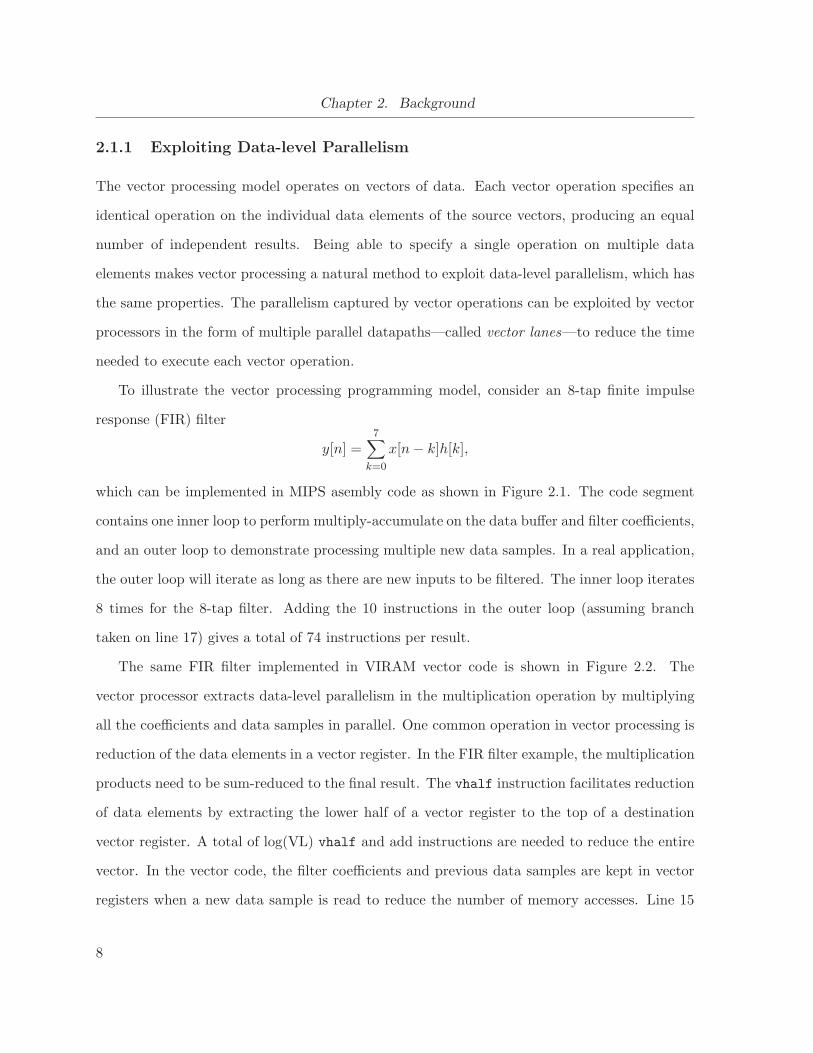
To illustrate the vector processing programming model, consider an 8-tap finite impulse
response (FIR) filter
y[n] =7
∑
k=0
x[n − k]h[k],
which can be implemented in MIPS asembly code as shown in Figure 2.1. The code segment
contains one inner loop to perform multiply-accumulate on the data buffer and filter coefficients,
and an outer loop to demonstrate processing multiple new data samples. In a real application,
the outer loop will iterate as long as there are new inputs to be filtered. The inner loop iterates
8 times for the 8-tap filter. Adding the 10 instructions in the outer loop (assuming branch
taken on line 17) gives a total of 74 instructions per result.
The same FIR filter implemented in VIRAM vector code is shown in Figure 2.2. The
vector processor extracts data-level parallelism in the multiplication operation by multiplying
all the coefficients and data samples in parallel. One common operation in vector processing is
reduction of the data elements in a vector register. In the FIR filter example, the multiplication
products need to be sum-reduced to the final result. The vhalf instruction facilitates reduction
of data elements by extracting the lower half of a vector register to the top of a destination
vector register. A total of log(VL) vhalf and add instructions are needed to reduce the entire
vector. In the vector code, the filter coefficients and previous data samples are kept in vector
registers when a new data sample is read to reduce the number of memory accesses. Line 15
8
.L10: ; Loop while new inputs receivedmov r6, zero ; Zero summov r4, sp ; Load address of sample buffermovi r5, 8 ; Set number of taps
.L8: 5
ldw r12, 0(r4) ; Load data from bufferldw r3, 100(r4) ; Load coefficientaddi r5, r5, −1addi r4, r4, 4mul r2, r12, r3 ; Multiply 10
add r6, r6, r2 ; Accumulatebne r5, zero, .L8
stw r6, 0(r9) ; Store filter resultstw r11, 0(r7) ; Store new sample to buffer 15
addi r7, r7, 4 ; Increment buffer positionbgeu r10, r7, .L4 ; Check for end of buffermov r7, sp ; Reset new sample pointer
.L4:addi r8, r8, −1 20
addi r9, r9, 4bne r8, zero, .L10
Figure 2.1: 8-tap FIR filter MIPS assembly
to 21 of Figure 2.2 stores the reduced result to memory, shifts the filter data elements by one
position using a vector extract opertaion to align them with the coefficients, and copies a new
data element from the scalar core. A total of 18 instructions are needed to calculate a single
result. The capitalized instructions are specific to the VIRAM implementation of the FIR filter,
and can be compared to Figure 3.7 for differences between the VIRAM and soft vector processor
implementations.
The vector code has a significant advantage over the MIPS code in terms of the number of
instructions executed. Scaling the FIR filter example to 64 filter taps, the MIPS code would
require executing 522 instructions, while the vector code would still only execute 18 instructions,
but have a different value of VL.
9

Chapter 2. Background
vmstc vbase0, sp ; Load base addressvmstc vbase1, r3 ; Load coefficient addressvmstc VL, r2 ; Set VL to num tapsvld.h v2, vbase1 ; Load filter coefficientsvld.h v1, vbase0 ; Load input vector 5
.L5:VMULLO.VV v3, v0, v2 ; Multiply data and coefficientsVHALF v4, v3 ; Extract half of the vectorVADD.VV v3, v4, v3 ; VL is automatically halved by vhalfVHALF v4, v3 10
VADD.VV v3, v4, v3VHALF v4, v3 ; 3 half−reductions for 8 tapsVADD.VV v3, v4, v3vmstc VL, r9 ; Reset VL to num taps (vhalf changes VL)
15
vmstc vindex, r8 ; Set vindex to 0vext.vs r10, v3 ; Extract final summation resultstw r10, 0(r4) ; Store resultVMSTC vindex, r7 ; Set vindex to 1VEXT.VV v1, v1 ; Shift vector up 1 20
vmstc vindex, r6 ; Set vindex to NTAP−1vins.vs v1, r5 ; Insert new sampleaddi r3, r3, −1addi r4, r4, 4bne r3, zero, .L5 25
Figure 2.2: 8-tap FIR filter VIRAM vector assembly
2.1.2 Vector Instruction Set Architecture
Vector instructions are a compact way to encode large amounts of data parallelism, each speci-
fying tens of operations and producing tens of results at a time. Modern vector processors like
the Cray X1 use a register-register architecture similar to RISC processors [8]. Source operands
are stored in a large vector register file that can hold a moderate number of vector registers,
each containing a large number of data elements.
A vector architecture contains a vector unit and a separate scalar unit. The scalar unit is
needed to execute non-vectorizable portions of the code, and most control flow instructions. In
many vector instruction sets, instructions that require both vector and scalar operands, such
as adding a constant to a vector, also read from the scalar unit.
10
Vector addressing modes can efficiently gather and scatter entire vectors to and from mem-
ory. The three primary vector addressing modes are: unit stride, constant stride, and indexed
addressing. Unit stride accesses data elements in adjacent memory locations, constant stride ac-
cesses data elements in memory with a constant size separation between elements, and indexed
addressing accesses data elements by adding a variable offset for each element to a common
base address.
Vector instructions are controlled by a vector length (VL) register, which specifies the
number of elements within the vector to operate on. This vector length register can be modified
on a per-instruction basis. A common method to implement conditional execution is using
vector flag registers as an execution mask. In this scheme, a number of vector flag registers are
defined in addition to the vector registers, and have the same vector length such that one bit in
the vector flag register is associated with each data element. Depending on this one bit value,
the operation on the data element will be conditionally executed. Some instructions use the
flag register slightly differently. For example the vector merge instruction uses the bit value in
the flag register to choose between two source registers.
Besides inter-vector operations, vector instruction sets also support intra-vector operations
that manipulate data elements within a vector. Implementing these instructions are, however,
tricky, as they generally require inter-lane communication due to partitioning of data elements
over multiple lanes. For example, the VIRAM instruction set implements a number of instruc-
tions like vhalf, vhalfup, and vhalfdn to support element permutations.
2.1.3 Microarchitectural Advantages of Vector Processing
The previous sections have already illustrated the ease-of-use and instruction set efficiency of
the vector programming model. Vector processing also has many advantages that simplify the
vector processor microarchitecture. Vector instructions alleviate bottlenecks in instruction issue
by specifying and scheduling tens of operations, which occupy the processor for many cycles at
a time. This reduces instruction bandwidth needed to keep the functional units busy [9]. Vector
11

Chapter 2. Background
instructions also ease dependency checking between instructions, as the data elements within a
vector instruction are guaranteed to be independent, so each vector instruction only needs to
be checked once for dependencies before issuing. By replacing entire loops, vector instructions
eliminate loop control hazards. Finally, vector memory accesses are effective against the ever-
increasing latency to main memory, as they are able to amortize the penalty over the many
accesses made in a single memory instruction. This makes moderate-latency, high-throughput
memory technologies such as DDR-SDRAM good candidates for implementing main memory
for vector processors.
2.2 Vector Processors and SIMD Extensions
Having discussed the merits of vector processing, the following sections will describe a number
of single-chip and FPGA-based vector processors in literature, and briefly explain processors
based on vector-inspired SIMD processing. SIMD processing is a more limited form of the
vector computing model. The most well-known usage of SIMD processing is in multimedia
instruction extensions common in mainstream microprocessors. Recent microprocessors from
Intel, IBM, and some MIPS processors all support SIMD extensions.
2.2.1 SIMD Extensions
SIMD extensions such as Intel SSE and PowerPC AltiVec are oriented towards short vectors.
Vector registers are typically 128 bits wide for storing an entire vector. The data width is
configurable from 8 to 32 bits, allowing vector lengths to range from 16 (8 bits) to 4 (32 bits).
SIMD instructions operate on short, fixed-length vectors, and each instruction typically executes
in a single cycle. In contrast, vector architectures have a vector length register that can be
used to modify the vector length during runtime, and one vector instruction can process a long
vector over multiple cycles. In general, SIMD extensions lack support for strided memory access
patterns and more complex memory manipulation instructions, hence they must devote many
12
instructions to address transformation and data manipulation to support the few instructions
that do the actual computation [10]. Full vector architecture mitigates these effects by providing
a rich set of memory access and data manipulation instructions, and longer vectors to keep
functional units busy and reduce overhead [11].
2.2.2 Single-chip Vector Processors
The Torrent T0 [12] and VIRAM [6] are single-chip vector microprocessors that support a
complete vector architecture and are implemented as custom ASICs. T0 is implemented in
full-custom 1.0 µm CMOS technology. The processor contains a custom MIPS scalar unit, and
the vector unit connects to the MIPS unit as a co-processor. The vector unit has 16 vector
registers, a maximum vector length of 32, and 8 parallel vector lanes. VIRAM is implemented in
0.18 µm technology and runs at 200MHz. It has 32 registers, a 16-entry vector flag register file,
and two ALUs replicated over 4 parallel vector lanes. VIRAM has been shown to outperform
superscalar and VLIW architectures in the consumer and telecommunications categories of the
EEMBC [13] benchmarks by a wide margin [14]. These two vector processors share the most
similarity in processor architecture to this work.
RSVP [15] is a reconfigurable streaming vector coprocessor implemented in 0.18 µm technol-
ogy, and was shown to achieve speedup of 2 to 20 times over its ARM9 host processor alone on
a number of embedded kernel benchmarks. Some other vector architectures proposed recently
for ASIC implementation are the CODE architecture [16] which is based on multiple vector
cores, and the SCALE processor based on the vector-thread architecture [17] that combines
multi-thread execution with vector execution. These two architectures were only studied in
simulation.
2.2.3 FPGA-based Vector Processors
There have been a few past attempts to implement vector processors in FPGAs. However, most
of them targeted only a specific application, or were only prototypes of ASIC implementations.
13

Chapter 2. Background
A vector computer is described in [18] that has pipelined 32-bit floating-point units augmented
with custom instructions for solving a set of sparse linear equations. The vector computer has
8 adders and multipliers, supports a vector length of 16, and has a 128-bit data bus that can
transfer four 32-bit words. Little additional information is given about the system other than it
was mapped to a Xilinx Virtex II FPGA. ProHos [19] is a vector processor for computing higher
order statistics. Its core is a pipelined MAC unit with three multipliers and one accumulator.
The processor is implemented on the RVC [20] platform consisting of five Xilinx 4000E devices,
and runs at 7.5MHz. The SCALE vector processor [17] was prototyped in an FPGA [21], but
no specific attempt was made to optimize the architecture or implementation for FPGAs.
Three vector processors that, similar to this work, were specifically designed for FPGAs are
described in [22], [23], and [24]. The first vector processor [22] consists of two identical vector
processors located on two Xilinx XC2V6000 FPGA chips. Each vector microprocessor runs at
70MHz, and contains a simplified scalar processor with 16 instructions, a vector unit consisting
of 8 vector registers, 8 lanes (each containing a 32-bit floating-point unit), and supports a max-
imum vector length (MVL) of 64. Eight vector instructions are supported: vector load/store,
vector indexed load/store, vector-vector and vector-scalar multiplication/addition. However,
only matrix multiplication was demonstrated on the system. Although the vector processor
presented in this thesis lacks floating-point support, it presents a more complete solution con-
sisting of full scalar unit (Nios II) and a full vector unit (based on VIRAM instructions) that
supports over 45 distinct vector instructions plus variations.
The second vector processor [23] was designed for Xilinx Virtex-4 SX and operated at
169MHz. It contains 16 processing lanes of 16-bit and 17 on-chip memory banks connected to a
MicroBlaze processor through fast simplex links (FSL). It is not clear how many vector registers
were supported. Compared to the MicroBlaze, speedups of 4–10× were demonstrated with four
applications (FIR, IIR, matrix multiply, and 8×8 DCT). The processor implementation seems
fairly complete.
The third vector processor [24] is a floating point processing unit based on the T0 archi-
14

tecture, and operated at 189MHz on a Xilinx Virtex II Pro device. It has 16 vector registers
of 32 bits and a vector length of 16. Three functional units were implemented: floating-point
adder, floating-point multiplier, and vector memory unit that interfaces to a 256-bit memory
bus. All three functional units can operate simultaneously, which together with the 8 parallel
vector lanes in the datapath, can achieve 3.02 GFLOPS. No control processor was included for
non-floating-point or memory instructions, and it is unclear whether addressing modes other
than unit-stride access were implemented.
A Softcore Vector Processor is also presented in [25] for biosequence applications. The pro-
cessor consists of an instruction controller that executes control flow instructions and broadcast
vector instructions to an array of 16-bit wide processing elements (PE). Compared to this the-
sis, it is a more limited implementation with less features and instructions, but like this thesis
it also argues for a soft vector processor core.
Many SIMD systems have also been developed for FPGAs. A SIMD system is presented
in [26] that is comprised of 2 to 88 processing elements built around DSP multiplier blocks on
a Altera Stratix FPGA, and controlled by a central instruction stream. The system utilizes
all the DSP blocks of an Altera Stratix EP1S80 FPGA, but only 17% of the logic resources.
Only matrix multiplication was illustrated on the system, but the actual implementation of the
application was not described. This system demonstrates the tremendous amount of parallelism
available on modern FPGAs for performing parallel computations.
2.3 Multiprocessor Systems
In contrast to vector processing systems, where everything executes in lock-step, multiprocessor
systems have become popular recently as a way to obtain greater performance. In particular,
FPGA-based multiprocessors can be composed of multiple soft core1 processors, or a combi-
1Soft core processors are described fully in software, usually in HDL, and is synthesized into hardware andprogrammed into the device with the rest of the user design.
15

Chapter 2. Background
nation of soft and hard core2 processors. The parallelism in multiprocessor systems can be
described as multiple instruction multiple data (MIMD). Each processor in a MIMD multi-
processor system has its own instruction memory and executes its own instruction stream and
operates on different data. In contrast, SIMD systems have a single instruction stream that
is shared by all processors. For example, vector processing is a type of SIMD system. In the
context of soft processor acceleration, the discussion will focus on multiprocessor systems that
utilize multiple soft processors on FPGAs.
Most multiprocessor systems that have been implemented in FPGAs are unique as there
are not yet any de facto or formal standards. They usually differ in number of processors,
interconnect structure, how processors communicate, and how they access memory. However,
the communication scheme in multiprocessor systems can generally be categorized into shared
memory or message passing, and the memory architecture can be categorized as either central-
ized or distributed [27].
FPGA-based multiprocessor systems can be very flexible, allowing them to adapt to accel-
erate heterogeneous workloads that otherwise do not parallelize effectively. Specialized systems
with unique architectures can be designed to exploit the characteristics of a particular appli-
cation for better performance. For example, the multiprocessor system in [28] for LU matrix
factorization has a unique architecture that consists of a system controller that connects to a
number of processing elements in a star topology, and seven kinds of memory for communicat-
ing data and storing instructions. The IPv4 packet forwarding system in [29] has 12 MicroBlaze
processors arranged in four parallel pipelines of processors with each stage performing a specific
task. Table 2.1 lists a number of FPGA multiprocessor systems found in literature and their
features.
The disadvantage of MIMD multiprocessor systems is their complexity. Significant hard-
ware knowledge is needed to design a multiprocessor system, including consideration of issues
2Hard core processors are implemented directly in transistors in the device, separate from the user designwhich is programmed into the programmable logic fabric.
16

Multiprocessor Application # CPUs Speedup Communication MemoryCerberO [30] Discrete wavelet transform 4 4 Shared memory CentralizedKulmala [31] MPEG-4 encoding 4 1–3 Shared memory CentralizedMartina [32] Digital signal processing 8 7–8 Shared memory CentralizedRavindran [29] IPv4 packet forwarding 16 n/a Message-passing DistributedSoCrates [33] General purpose 2 n/a Shared memory DistributedWang [28] Matrix operations 6 4 Shared memory Distributed
Table 2.1: Partial list of FPGA-based multiprocessor systems in literature
such as interconnect, memory architecture, cache coherence and memory consistency protocols.
Creating a custom multiprocessor system architecture to tailor to the needs of a particular ap-
plication can be a daunting task due to the large design space. On the software front, the user
will need parallel programming knowledge to use these systems, which is not within the skillset
of the average software developer. Specialized multiprocessor systems add further difficulty of
writing software to effectively take advantage of the architecture.
2.4 Custom-designed Hardware Accelerators
Hardware accelerators are frequently used in conjunction with soft processors to accelrate cer-
tain portions of an application. Traditionally these accelerators are designed manually in HDL
by a hardware designer, and connect to the processor via an interface specified by the processor
vendor. The next two sections describe two different methods of interfacing custom-designed
hardware accelerators to a soft processor. The fundamental disadvantage of these accelerators
is they require hardware design effort to implement, verify, and test. Each accelerator, in most
cases, also performs only one function. Hence for each portion of the application to accelerate,
a different hardware accelerator is needed. This adds further time and design effort.
2.4.1 Decoupled Co-processor Accelerators
The co-processor accelerator model is akin to the use of floating-point co-processors in early
computer systems. These accelerators are decoupled from the main processor in operation.
17
Chapter 2. Background
The processor provides inputs to start the accelerator, then has the option of executing a
different part of the program while the accelerator is running, and finally reads results when
they are computed. This is the model adopted by the Xilinx MicroBlaze to interface to custom
co-processor accelerators. The MicroBlaze interfaces to accelerators through 16 32-bit Fast
Simplex Link (FSL) channels, which are unidirectional point-to-point first in first out (FIFO)
communication buffers. The MicroBlaze CPU uses blocking or non-blocking reads and writes
to access the FSL channels, and can use up to 8 FSL channels for outputs from the CPU, and
8 FSL channels for inputs to the CPU.
Co-processor accelerators have the advantage that they are decoupled from the main CPU
core, allowing both the CPU and accelerator to execute concurrently. Adding co-processor
accelerators are less likely to negatively impact the performance of the CPU core compared
to more tightly-coupled methods due to their decoupled nature. The design tools also tend to
have good support for these accelerators, allowing the programmer to interact with them as
easily as calling a function, and without having to write parallel programs. As an example,
the MicroBlaze FSL provides simple send and receive functions to communicate with multiple
accelerators. Co-processor accelerators also have the advantage that they can act as data master
and communicate directly to memory. However, it is frequently up to the user to create the
interface manually, which is added work.
2.4.2 Custom Instruction Accelerators
An alternate connection scheme interfaces an accelerator as a custom logic block within the
processor’s datapath, in parallel to the processor’s main ALU. This scheme allows an accel-
erator to fetch operands directly from the processor’s register file, and write results back to
the processor’s register file using the ALU’s result bus. These accelerators effectively extend
the functionality of the processor’s ALU. The Nios II CPU supports this type of accelerator as
custom instructions to the processor. To control the custom accelerators, new instructions are
added to the processor, mapping to an unused opcode in the Nios II ISA. These instructions
18
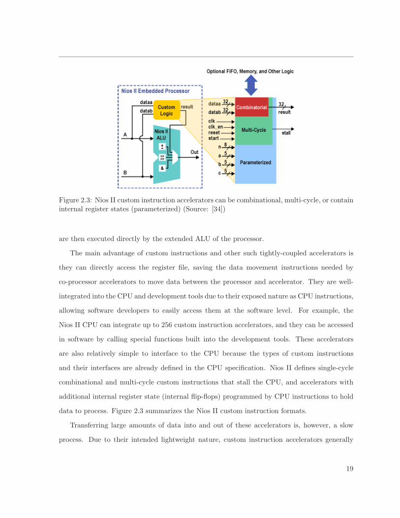
Figure 2.3: Nios II custom instruction accelerators can be combinational, multi-cycle, or containinternal register states (parameterized) (Source: [34])
are then executed directly by the extended ALU of the processor.
The main advantage of custom instructions and other such tightly-coupled accelerators is
they can directly access the register file, saving the data movement instructions needed by
co-processor accelerators to move data between the processor and accelerator. They are well-
integrated into the CPU and development tools due to their exposed nature as CPU instructions,
allowing software developers to easily access them at the software level. For example, the
Nios II CPU can integrate up to 256 custom instruction accelerators, and they can be accessed
in software by calling special functions built into the development tools. These accelerators
are also relatively simple to interface to the CPU because the types of custom instructions
and their interfaces are already defined in the CPU specification. Nios II defines single-cycle
combinational and multi-cycle custom instructions that stall the CPU, and accelerators with
additional internal register state (internal flip-flops) programmed by CPU instructions to hold
data to process. Figure 2.3 summarizes the Nios II custom instruction formats.
Transferring large amounts of data into and out of these accelerators is, however, a slow
process. Due to their intended lightweight nature, custom instruction accelerators generally
19

Chapter 2. Background
do not define their own memory interface (although it can be done manually by the designer).
Instead, they rely on the processor to perform memory access. In the Nios II case, custom
instructions can only read up to two 32-bit operands from the processor register file and write
one 32-bit result per instruction, like other Nios II R-type instructions. Another drawback is
the accelerators lie on the critical path of the processor ALU. Adding one or more accelerators
with complex combinational logic can unnecessarily reduce the maximum frequency of the CPU
core, affecting performance of the entire system.
2.5 Synthesized Hardware Accelerators
Synthesized hardware accelerators use behavioural synthesis techniques to automatically create
hardware accelerators from software. These accelerators and processor systems take on different
architectures, and several of them will be described in this section. A common drawback of
these approaches is since the tools synthesize hardware from the user’s software application,
if the user changes hardware-accelerated sections of the software, the register transfer level
(RTL) description of the hardware accelerators, and possibly of the entire system, will have to
be regenerated and recompiled. This can make it difficult to achieve a targeted clock frequency
for the whole design, for example. Synthesis tools also generally create separate hardware
accelerators for each accelerated function, with no opportunity for resource sharing between
accelerators.
2.5.1 C-based Synthesis
Hardware circuits synthesized from software written in the C programming language or vari-
ations of it has long been advocated due to the widespread use of C in embedded designs.
Although the idea is attractive, in reality there are many difficulties such as identifying and
extracting parallelism, scheduling code into properly timed hardware, and analyzing commu-
nication patterns and pointer aliasing [35]. Due to these difficulties, C-based synthesis tools
20
usually do not support full American National Standards Institute (ANSI) C, but only a subset,
or employ extensions to the language. For example, floating-point data types are often not sup-
ported due to the hardware complexity required. With current automatic synthesis methods,
the user also needs to have a good understanding of how to write “C” code that synthesizes
efficiently to hardware. Unfortunately, the rules and language subsets often change from one
tool to the next.
Given these limitations, C-based synthesis is still a powerful method for creating hardware
accelerators, which can be seen from the large number of solutions in this area. The follow-
ing sections will describe three compilers that support FPGAs: Altera C2H Compiler, Xilinx
CHiMPS, and Catapult C. Descriptions of some other C-based synthesis tools can be found
in [36].
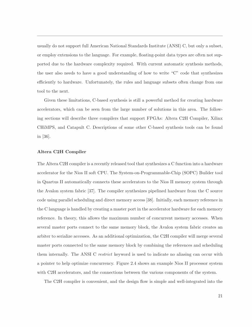
Altera C2H Compiler
The Altera C2H compiler is a recently released tool that synthesizes a C function into a hardware
accelerator for the Nios II soft CPU. The System-on-Programmable-Chip (SOPC) Builder tool
in Quartus II automatically connects these accelerators to the Nios II memory system through
the Avalon system fabric [37]. The compiler synthesizes pipelined hardware from the C source
code using parallel scheduling and direct memory access [38]. Initially, each memory reference in
the C language is handled by creating a master port in the accelerator hardware for each memory
reference. In theory, this allows the maximum number of concurrent memory accesses. When
several master ports connect to the same memory block, the Avalon system fabric creates an
arbiter to serialize accesses. As an additional optimization, the C2H compiler will merge several
master ports connected to the same memory block by combining the references and scheduling
them internally. The ANSI C restrict keyword is used to indicate no aliasing can occur with
a pointer to help optimize concurrency. Figure 2.4 shows an example Nios II processor system
with C2H accelerators, and the connections between the various components of the system.
The C2H compiler is convenient, and the design flow is simple and well-integrated into the
21

Chapter 2. Background
Figure 2.4: Example Nios II system with C2H accelerators (Source: [38]).
development tools. The pipelined, decoupled co-processors do not have the disadvantages of
tightly-coupled custom instruction accelerators, and direct memory access is a powerful feature
that further simplifies usage. Despite its ease of use, the performance of the automatically
synthesized accelerators are not as good as one might presume. The C2H compiler generates
only a single solution in the design space. It has no option to control the amount of loop unrolling
to set the performance and resource level of the accelerator. As can be seen from Figure 2.4, if
one of the accelerators have to access multiple data elements from a single data memory, it will
be forced to serialize the memory accesses, possibly creating a bottleneck in the accelerator.
To alleviate this bottleneck, data needs to be partitioned efficiently over multiple memories to
reduce overlap. However, this is a step that needs to be done manually by the user, and requires
22

a good understanding of the hardware system and application. The hardware accelerators also
do not have caches, nor do they support cache coherency with the Nios II processor’s cache.
The user either has to ensure that data does not overlap, or force the processor to flush its
cache before transferring execution to the accelerator.
CHiMPS Target Language
Compiling HLL Into Massively Pipelined Systems (CHiMPS) is an experimental compiler by
Xilinx Labs [39] that compiles high level languages such as C into hardware accelerators that can
be implemented on Xilinx FPGAs. The compiler uses the CHiMPS Target Language (CTL),
which is a predefined instruction set, as an intermediate language for synthesis, then extracts
a dataflow graph from the CTL. This dataflow graph is then implemented in hardware, and
pipelined for performance. One additional feature of CHiMPS is it automatically generates
caches to cache data inside the FPGA, and supports coherency between multiple cache blocks
and multiple FPGAs. Few additional details have been released about CHiMPS, and it is still
unclear what further functionality it provides.
Catapult Synthesis
Catapult Synthesis [40] by Mentor Graphics synthesizes ANSI C++ into an RTL description
that can then be targeted to an ASIC or FPGA. Catapult Synthesis can actually synthesize
entire systems without processor cores, and it has been used to design production ASIC and
FPGA designs [40]. The tool automatically generates multiple microarchitectures for a given
design, allowing the user to explore performance, area, and power tradeoffs. The user can use
synthesis directives to specify high-level decisions. A number of main architectural transfor-
mations are applied to generate a hardware architecture. Interface synthesis converts the way
the C function communicates with the rest of the design, variable and array mapping controls
how variables are mapped to registers or memory, loop pipelining allows multiple iterations of
a loop to execute in parallel, loop unrolling exploits parallelism across subsequent loop itera-
23

Chapter 2. Background
tions, and scheduling transforms the untimed C code into an architecture with a well-defined
cycle-by-cycle behaviour.
The Catapult Synthesis tool allows designers to automate parts of the detailed implementa-
tion of a design, while the automatic exploration process allows them to explore tradeoffs in the
implementation. However, the user must still specify how data is transferred to and from the
accelerator during interface synthesis, and use directives to guide the other phases of compila-
tion. User experience reports [41] emphasize that the user must have a good understanding of
the algorithm and implications of different C/C++ constructs to generate good hardware. As
Catapult Synthesis is designed to synthesize entire systems, it does not have natural support
for connecting to a processor.
2.5.2 Block-based Synthesis
Block-based synthesis describes methods that synthesize hardware from a graphical design
environment that allows the user to design systems by graphically connecting functional blocks.
This synthesis flow is frequently incorporated into model-based design environments, in which
the user creates a high-level executable specification using functional blocksets to define the
desired functional behaviour with minimal hardware detail. This executable specification is
then used as a reference model while the hardware representation is further specified. The most
commonly used such environment is the Mathworks Simulink design environment. This design
method allows algorithm designers and hardware designers to work in a common environment,
and allows architectural exploration without specifying detailed implementation. Automated
synthesis methods from these environments simplify the final implementation phase, bridging
the gap between algorithm and hardware designers.
The following subsections will describe four specific tools: Xilinx System Generator for DSP,
Altera DSP Builder, Simulink HDL Coder, and Starbridge Viva. Starbridge Viva is the only
solution of the four that does not operate within Simulink. Another similar tool that interfaces
to Simulink is DSPLogic Reconfigurable Toolbox [42].
24
Xilinx System Generator for DSP & Altera DSP Builder
The Xilinx System Generator for DSP [43] is an add-on that uses Simulink as a front-end to
interface to Xilinx IP cores for DSP applications. The Xilinx Blockset includes over 90 common
DSP building blocks that interface to Xilinx IP core generators. The System Generator also
allows hardware co-simulation of the Simulink model using a Xilinx FPGA-based DSP platform
communicating through ethernet or JTAG to accelerate the simulation.
The Altera DSP Builder has mostly the same features as the Xilinx System Generator but
is targeted to Altera FPGAs. Pre-designed DSP blocks from the Altera MegaCore functions
can be imported into the Simulink design, and the system can be co-simulated using an Altera
FPGA through JTAG. The DSP Builder also has blocks for communicating with the Avalon
fabric so the accelerators generated by DSP Builder can be instantiated in SOPC Builder
systems, and used with the Nios II soft processor.
The advantage of these vendor-specific block libraries is they are highly optimized to the
vendor’s platform. But since they are specific to a target platform, the Simulink models gener-
ated using these flows are no longer platform independent and suffer in portability.
Simulink HDL Coder
Simulink HDL Coder [44] generates synthesizable Verilog or VHDL code from Simulink models
and Embedded MATLAB [45] code for datapath implementations, as well as from finite-state
machines described with the Stateflow tool for control logic implementations. The generated
HDL is target independent, bit-exact and cycle-accurate to the Simulink model, and can be
implemented on FPGA or ASIC. The tool is a mix of synthesis and a set of supported Simulink
models with HDL code. Over 80 Simulink models are supported in version 1.0, with multiple
implementations included for some commonly used blocks. The HDL Coder can automatically
pipeline Embedded MATLAB function blocks and state machines.
25

Chapter 2. Background
Starbridge Viva
Starbridge Viva [46] provides its own drag and drop graphical and object oriented environment
for algorithmic development. A parallel algorithm can be modelled by connecting functional
objects on a design pallet using transports that represent the data flow. Objects are “poly-
morphic” and can be used with different data types, data rates, and data precisions allowing
reuse and experimentation with design tradeoffs. Built-in objects are, however, relatively prim-
itive constructs like comparators and registers compared to Simulink blocks or DSP blocks in
the Xilinx/Altera tools. The software supports a number of reconfigurable high-performance
computing (HPC) systems with both FPGA and CPUs, as well as the vendor’s own Starbridge
Hypercomputers.
2.5.3 Application Specific Instruction Set Processor
Application-specific instruction set processors (ASIPs) have configurable instruction sets that
allow the user to extend the processor by adding custom hardware accelerators and instructions.
They provide a similar level of configurability as soft processors with custom instructions on
FPGAs, but are configured only once before being inserted into an ASIC flow. Adding cus-
tom hardware and instructions to ASIPs, however, frequently requires the use of proprietary
synthesis languages and compilers. They also share the common disadvantages of synthesized
hardware accelerators of requiring separate accelerators for each accelerated function. The Ten-
silica Xtensa processor will be described in the next section. Another commercial ASIP is the
ARC configurable processor [47].
Tensilica Xtensa
The Tensilica Xtensa [48] processor is a configurable and extensible processor for ASIC and
FPGA design flows. It allows the customer to configure the processor to include or omit features,
and add application-specific extensions to the base processor using the Tensilica Instruction
Extension language (TIE). These instructions expand the base instruction set of the processor.
26
TIE is flexible and can be used to describe accelerators that range from multi-cycle pipelined
hardware to VLIW, SIMD, and vector architectures. The Tensilica XPRES (Xtensa PRocessor
Extension Synthesis) Compiler [49] furthermore creates TIE descriptions from ANSI C/C++
code, allowing direct generation of processor hardware RTL from C/C++ specification. It
also allows design space exploration by generating different TIE source files that represent a
range of Xtensa processors that trade off performance of the application versus area. However,
accelerators generated from TIE are optimized for ASIC and not for FPGA implementation.
FPGA support is mainly provided for validation purposes.
2.5.4 Synthesis from Binary Decompilation
Another method of synthesizing hardware accelerators is by binary decompilation techniques
that decompile the software binary, and synthesize hardware accelerators from the resulting
assembly instructions or description. Two commercial products in this category are Cascade [50]
by CriticalBlue and Binachip-FPGA [51]. There are not many details on the performance of
Binachip-FPGA, but simulation results reported in [52] of hardware accelerator synthesis from
binary decompilation and mapping to a microprocessor plus FPGA system-on-chip are less than
impressive. CriticalBlue adopts a different architecture for its accelerators to achieve higher
performance, as will be described in the following section.
CriticalBlue Cascade
Cascade by CriticalBlue is another tool that automatically synthesizes co-processors to a
main processor for SoC, structured ASIC, and Xilinx FPGA platforms. Cascade differs from
synthesis-based solutions described in previous sections in that it synthesizes a co-processor
by analyzing the compiled object code of an application. The Cascade co-processor has a
distinct VLIW processor architecture, different from other dataflow or custom-hardware and
loop-pipelining based co-processors such as CHiMPS and the Altera C2H compiler. The co-
processor connects to the main CPU via the bus interface of the main processor, and can be
27
Chapter 2. Background
configured as a slave co-processor of the main CPU, or an autonomous streaming co-processor
with direct memory access. It is customizable, and the tool automatically performs architec-
ture exploration by generating a range of co-processors with different performance and area.
Furthermore, it has options to configure the instruction format and control the amount of
instruction decode logic. A single co-processor can also be reused to accelerate multiple non-
overlapping portions of an application. The VLIW architecture is, however, not ideal for FPGA
implementation, as will be explained in Section 2.6.2.
2.6 Other Soft Processor Architectures
Rather than offloading sections of an application from the soft processor to a hardware acceler-
ator or co-processor to speed up execution, the soft processor itself can be improved to achieve
higher performance without the addition of accelerators. More advanced architectures than
standard RISC architectures have been explored for soft processors, and several of these will
be described in the following sections.
2.6.1 Mitrion Virtual Processor
The Mirion Virtual Processor by Mitrionics [53] is a fine-grained, massively parallel, config-
urable soft core processor. It is based on a collection of ALU tiles that each perform a different
function, and are interconnected by a network. The processor is progammed in the proprietary
Mitrion-C programming language, which has C-like syntax and allows the programmer to iden-
tify parallelism within the code. The user can partially control resource usage by selecting the
level of loop unroll in the application. The compiler and configurator then analyzes the applica-
tion source code, and generates a configuration of the processor that executes the application.
Currently, the processor is supported on Xilinx FPGAs.
Although the processor and tools provide a complete solution to automatically synthesize
a system to execute the user application, similar to synthesized hardware accelerators, the
28
processor has to be reconfigured whenever the application changes, due to the code-specific
nature of the processor configurator.
2.6.2 VLIW Processors
VLIW architectures have also been used in FPGAs for acceleration. VLIW soft processors like
[54] are designed for a specific application, while others like [55–57] are more general purpose.
The 4-way VLIW processor described in [56] has four identical, general-purpose functional
units, connected to a single, multi-ported, 32 × 32-bit register file. It supports automatically
generated custom hardware units that can be placed inside each of the identical ALUs. A similar
VLIW processor in architecture is [57], which is configurable and is automatically generated by
a configuration tool. It has multiple heterogeneous functional units, but also supports custom
hardware units coded in VHDL. The register file is separated into three smaller register files for
address, data, and data to custom hardware units. Each of the smaller register files are further
separated into even and odd register banks to reduce the number connections.
Another FPGA-based VLIW processor is the VPF [58], which is a simplified version of the
EVP [59] ASIC. Each funtional unit in the VLIW architecture is itself a SIMD unit that can
processes a number of 16-bit operands, with the SIMD width configurable at compile time.
The processor has three functional units: MAC, shuffle, and load/store, and seems relatively
complete with 52 instructions. A 200MHz clock frequency was achieved for SIMD width of 4
and 8, and performance degrades significantly past SIMD width of 16, mainly due to the shuffle
unit which allows arbitrary permutation of data elements across the SIMD unit.
A model of the Intel Itanium microarchitecture supporting a subset of the Itanium ISA was
also prototyped on an FPGA [60].
The drawback of VLIW archtiectures for FPGAs is the multiple write ports required in the
register file to support multiple functional units. Since embedded memory blocks on current
FPGAs have only two ports, and one is needed for reading, a register file with multiple write
ports is commonly implemented either as a collection of discrete registers as in [56], or divided
29

Chapter 2. Background
into multiple banks as in [57]. In either case, multiplexers are needed at the write side to connect
multiple functional units to the register file, and this overhead increases as the processor is made
wider with more functional units to exploit parallelism. For multiple bank implementations,
there are additional restrictions on which registers can be written to by each instruction.
2.6.3 Superscalar Processors
The PowerPC 440 core on Xilinx Virtex 5 devices has a superscalar pipeline, but it is a hard
processor core implemented in transistors inside the FPGA device, and does not provide the
level of customization available in soft core processors. However, the Auxilliary Processor Unit
(APU) does allow the PowerPC core to connect to custom co-processors implemented in the
FPGA fabric.
FPGAs are frequently used to prototype ASIC microprocessors, and recently there has
been interest in using FPGAs to more quickly and accurately explore microprocessor design
space [61]. The Intel Pentium was implemented on an FPGA and connected to a complete
computer system for architectural exploration in [62], and a speculative out-of-order superscalar
core based on the SimpleScalar PISA was implemented in an FPGA in [63]. The lack of soft
superscalar processors specifically designed for FPGAs could be due to a number of difficulties
in mapping this type of architecture to FPGAs. Wide-issue superscalar processors require
complex dependency checking hardware to identify dependences during instruction decode, as
well as comparators to detect when operands are available so the instruction can be issued. The
data forwarding multiplexers that carry results from outputs of functional units to inputs also
add to complexity. And similar to VLIW processors, the register file of superscalar processors
also needs many read and write ports to support multiple functional units.
30

2.7 Summary
Each of the four categories of soft processor accelerators described in this chapter has its
advantages and drawbacks. Multiprocessor systems are very flexible with respect to the type
of application that can be accelerated, but are complex both to design and use. Custom-
designed hardware accelerators require significant hardware design knowledge and effort, and
generally require a separate accelerator for each accelerated function. Although synthesized
accelerators automatically create hardware accelerators from software, the accelerators have to
be regenerated and resynthesized when the software changes. An improved soft processor can
accelerate the entire application and does not require hardware design knowledge or effort to
use. However, current VLIW and superscalar soft processors implemented in FPGAs do not
scale well to high performance.
The next chapter will discuss in detail the design and architecture of the soft vector proces-
sor, an approach that combines the best advantages of most of these accelerator techniques.
31

Chapter 2. Background
32
Chapter 3
Configurable Soft Vector Processor
This chapter describes the design and implementation of the configurable soft vector processor,
targeted specifically to the Altera Stratix III FPGA. The chapter first outlines the require-
ments of an effective soft processor accelerator, and shows how the soft vector processor meets
these requirements. It then gives an overview of the processor, and presents the design and
implementation details. The novel features and instructions of the soft vector processor are
highlighted, and the improvements over the VIRAM instruction set are demonstrated using a
simple FIR filter example. Finally, the design flow of the soft vector processor is compared to
a commercial C-based synthesis flow, namely the Altera C2H compiler.
3.1 Requirements
The previous chapter described currently available soft processor accelerator solutions. Given
each of their advantages and drawbacks, an ideal soft processor accelerator that combines the
best of different solutions should:
• have scalable performance and resource usage,
• be simple to use, ideally requiring no hardware design effort,
• separate hardware and software design flows early in the design,
• allow rapid development by minimizing the number of times the design has to be synthe-sized, placed and routed.
Vector processing, in particular a soft vector processor, addresses all these requirements. It
provides a simple programming model that can be easily understood by software developers,
33
Chapter 3. Configurable Soft Vector Processor
and its application-independent architecture allows hardware and software development to be
separated. A soft vector processor delivers scalable performance and resource usage through soft
processor configurability and a scalable architecture. Modifying the application also requires
only changing the software and a software recompilation.
3.2 Soft Vector Architecture
The soft vector architecture is a configurable soft-core vector processor architecture developed
specifically for FPGAs. It leverages the configurability of FPGAs to provide many parameters
to configure the processor for a desired performance level, and for a specific application.
The soft vector processor instruction set borrows heavily from the instruction set of VIRAM,
but makes modifications to target embedded applications and FPGAs. In particular, the soft
vector processor removes support for virtual memory, floating-point data types, and certain
vector and flag manipulation instructions, but adds new instructions to take advantage of DSP
functionality and embedded memories in FPGAs. The following sections describe the high
level architecture of the soft vector processor, and how the instruction execution differs from
traditional vector processors.
3.2.1 System Overview
The soft vector architecture specifies a family of soft vector processors with varying performance
and resource utilization, and a configurable feature set to suit different applications. A software
configurator uses a number of parameters to configure the highly parameterized Verilog source
code and generate an application- or domain-specific instance of the processor. The configura-
bility gives designers flexibility to trade-off performance and resource utilization, and to further
fine-tune resource usage by removing unneeded processor features and instruction support.
Figures 3.1 illustrates the high level view of the soft vector processor. The architecture
consists of a scalar core, a vector processing unit, and a memory interface unit. The scalar
34
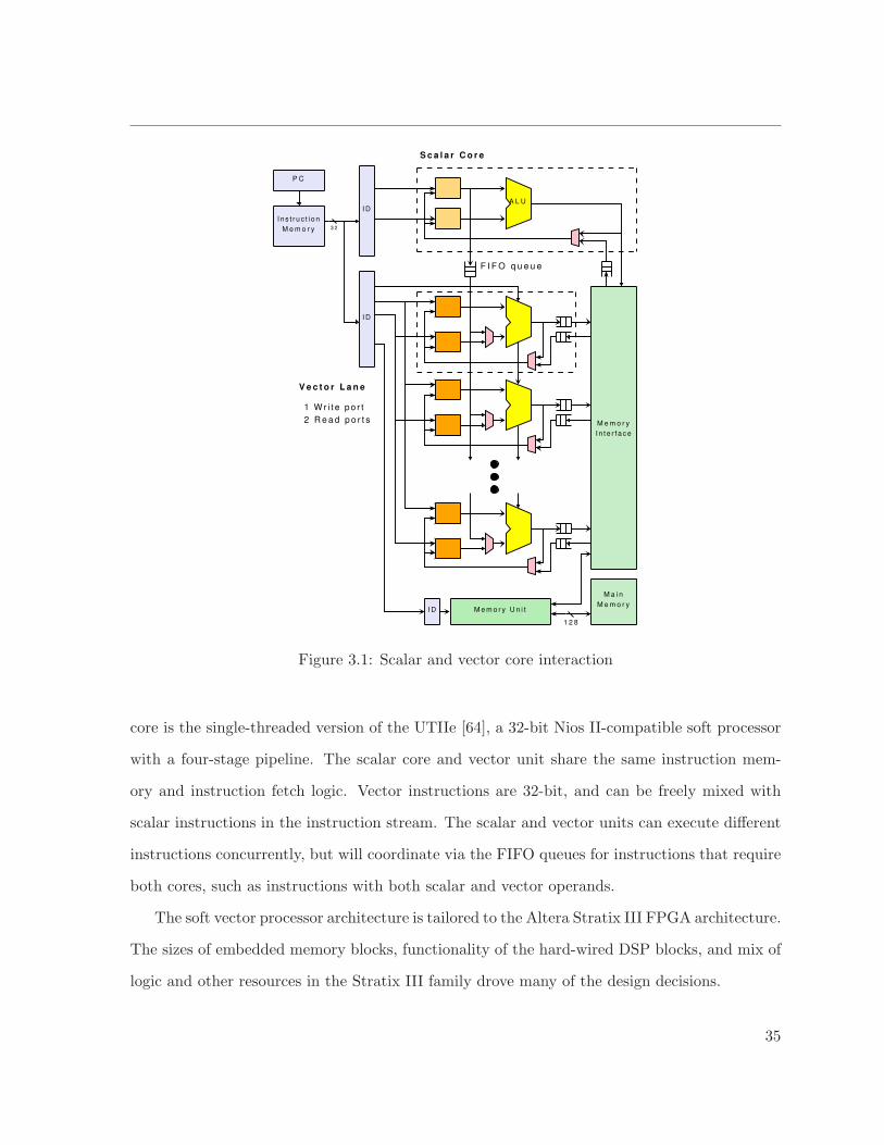
P C
I DA L U
I n s t r u c t i o n
M e m o r y 3 2
S c a l a r C o r e
M e m o r y
I n t e r f a c e
M e m o r y U n i t
F I F O q u e u e
1 W r i t e p o r t
2 R e a d p o r t s
V e c t o r L a n e
M a i n
M e m o r y
1 2 8
I D
I D
Figure 3.1: Scalar and vector core interaction
core is the single-threaded version of the UTIIe [64], a 32-bit Nios II-compatible soft processor
with a four-stage pipeline. The scalar core and vector unit share the same instruction mem-
ory and instruction fetch logic. Vector instructions are 32-bit, and can be freely mixed with
scalar instructions in the instruction stream. The scalar and vector units can execute different
instructions concurrently, but will coordinate via the FIFO queues for instructions that require
both cores, such as instructions with both scalar and vector operands.
The soft vector processor architecture is tailored to the Altera Stratix III FPGA architecture.
The sizes of embedded memory blocks, functionality of the hard-wired DSP blocks, and mix of
logic and other resources in the Stratix III family drove many of the design decisions.
35
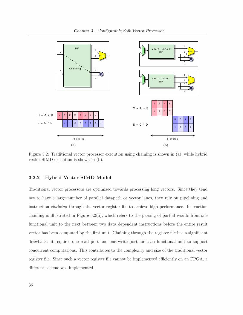
Chapter 3. Configurable Soft Vector Processor
9 c y c l e s
0 1 2 3 4 5 6 7
0 1 2 3 4 5 6 7
A
B
C
D
C
EC h a i n i n g
R F
C = A + B
E = C * D
(a)
A
B
C
D
A
B
C
D
0
1
2
3
4
5
6
7
0
1
2
3
4
5
6
7
8 c y c l e s
V e c t o r L a n e 0
R F
V e c t o r L a n e 1
R F
C = A + B
E = C * D
(b)
Figure 3.2: Traditional vector processor execution using chaining is shown in (a), while hybridvector-SIMD execution is shown in (b).
3.2.2 Hybrid Vector-SIMD Model
Traditional vector processors are optimized towards processing long vectors. Since they tend
not to have a large number of parallel datapath or vector lanes, they rely on pipelining and
instruction chaining through the vector register file to achieve high performance. Instruction
chaining is illustrated in Figure 3.2(a), which refers to the passing of partial results from one
functional unit to the next between two data dependent instructions before the entire result
vector has been computed by the first unit. Chaining through the register file has a significant
drawback: it requires one read port and one write port for each functional unit to support
concurrent computations. This contributes to the complexity and size of the traditional vector
register file. Since such a vector register file cannot be implemented efficiently on an FPGA, a
different scheme was implemented.
36
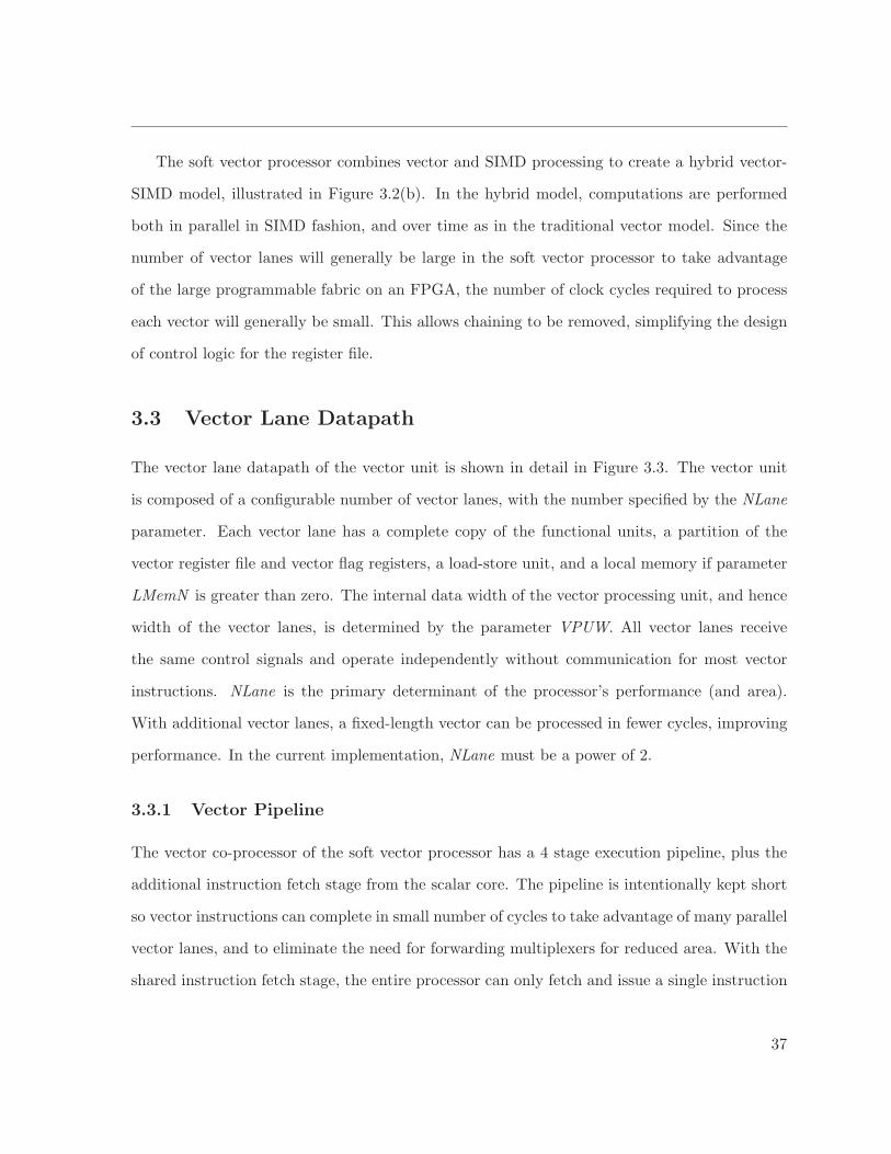
The soft vector processor combines vector and SIMD processing to create a hybrid vector-
SIMD model, illustrated in Figure 3.2(b). In the hybrid model, computations are performed
both in parallel in SIMD fashion, and over time as in the traditional vector model. Since the
number of vector lanes will generally be large in the soft vector processor to take advantage
of the large programmable fabric on an FPGA, the number of clock cycles required to process
each vector will generally be small. This allows chaining to be removed, simplifying the design
of control logic for the register file.
3.3 Vector Lane Datapath
The vector lane datapath of the vector unit is shown in detail in Figure 3.3. The vector unit
is composed of a configurable number of vector lanes, with the number specified by the NLane
parameter. Each vector lane has a complete copy of the functional units, a partition of the
vector register file and vector flag registers, a load-store unit, and a local memory if parameter
LMemN is greater than zero. The internal data width of the vector processing unit, and hence
width of the vector lanes, is determined by the parameter VPUW. All vector lanes receive
the same control signals and operate independently without communication for most vector
instructions. NLane is the primary determinant of the processor’s performance (and area).
With additional vector lanes, a fixed-length vector can be processed in fewer cycles, improving
performance. In the current implementation, NLane must be a power of 2.
3.3.1 Vector Pipeline
The vector co-processor of the soft vector processor has a 4 stage execution pipeline, plus the
additional instruction fetch stage from the scalar core. The pipeline is intentionally kept short
so vector instructions can complete in small number of cycles to take advantage of many parallel
vector lanes, and to eliminate the need for forwarding multiplexers for reduced area. With the
shared instruction fetch stage, the entire processor can only fetch and issue a single instruction
37
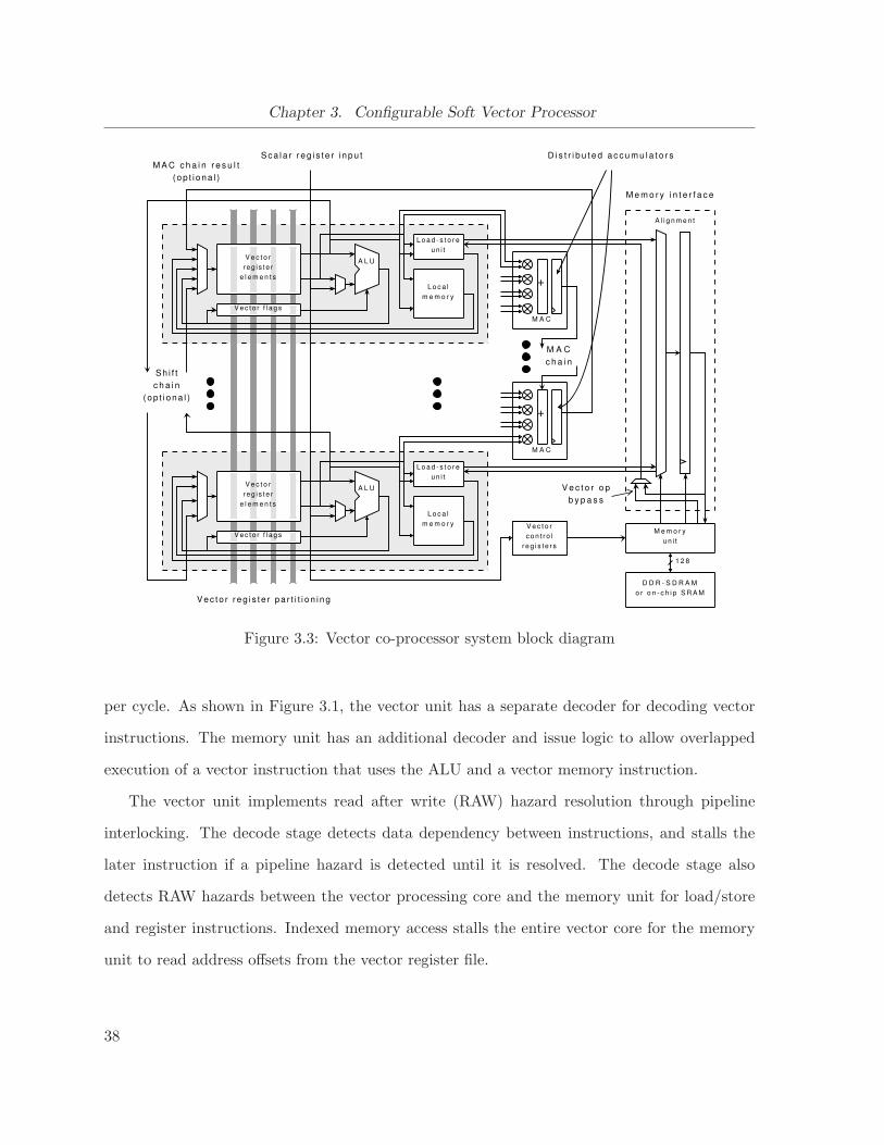
Chapter 3. Configurable Soft Vector Processor
+
M A C
+
M A C
A L U
L o a d - s t o r e
un i t
L o c a l
m e m o r y
V e c t o r
r e g i s t e r
e l e m e n t s
V e c t o r f l a g s
M e m o r y i n t e r f a c e
V e c t o r r e g i s t e r p a r t i t i o n i n g
S c a l a r r e g i s t e r i n p u t
A l i g n m e n t
1 2 8
V e c t o r o p
b y p a s s
A L U
L o a d - s t o r e
un i t
L o c a l
m e m o r y
V e c t o r
r e g i s t e r
e l e m e n t s
V e c t o r f l a g s
M A C
c h a i n
V e c t o r
c o n t r o l
r e g i s t e r s
M e m o r y
un i t
D D R - S D R A M
o r o n - c h i p S R A M
M A C c h a i n r e s u l t
( o p t i o n a l )
Sh i f t
c h a i n
( o p t i o n a l )
D i s t r i b u t e d a c c u m u l a t o r s
Figure 3.3: Vector co-processor system block diagram
per cycle. As shown in Figure 3.1, the vector unit has a separate decoder for decoding vector
instructions. The memory unit has an additional decoder and issue logic to allow overlapped
execution of a vector instruction that uses the ALU and a vector memory instruction.
The vector unit implements read after write (RAW) hazard resolution through pipeline
interlocking. The decode stage detects data dependency between instructions, and stalls the
later instruction if a pipeline hazard is detected until it is resolved. The decode stage also
detects RAW hazards between the vector processing core and the memory unit for load/store
and register instructions. Indexed memory access stalls the entire vector core for the memory
unit to read address offsets from the vector register file.
38
A L U O P [ 1 : 0 ]
A
B
z e r o B
c i n
c o u t
z e r o B 2
c i n 2
c o u t 2
se l [ 1 :0 ]
Z e r o
C o m p a r e
Z e r o
C o m p a r e
S e l e c t
L o g i c
A L U O P [ 5 : 0 ] F l a g
R e s u l t
Figure 3.4: Vector Lane ALU
3.3.2 Datapath Functional Units
The functional units within each vector lane datapath include an ALU, a single-cycle barrel
shifter, and a multiplier. The ALU takes advantage of the Stratix III ALM architecture to
implement an efficient adder/subtractor. Figure 3.4 shows how the ALU is implemented using
ALMs configured in arithmetic mode. The ALU supports arithmetic and logical operations,
maximum/minimum, merge, absolute value, absolute difference, and comparisons. The first
adder performs the bulk of the arithmetic operations, while the second adder is used for the
absolute difference instruction (to compute subtraction with inputs reversed), and for logical
operations (using the lookup tables at the adder inputs). The barrel shifter is implemented in
log(n) levels of multiplexers, and the multiplier is implemented using embedded DSP blocks.
The multiplier takes up one quarter of a DSP block in 16-bit operation, and half a DSP block
in 32-bit operation.
39

Chapter 3. Configurable Soft Vector Processor
3.3.3 Distributed Vector Register File
The soft vector processor uses a vector register file that is distributed across vector lanes. This
differs from traditional vector architectures which employ a large, centralized vector register file
with many ports. The vector register file is element-partitioned — each vector lane has its own
register file that contains all the vector registers, but only a few data elements of each vector
register [12]. The partitioning scheme naturally divides the vector register file into parts that
can be implemented using the embedded memory blocks on the FPGA. It also allows SIMD-like
access to multiple data elements in the vector register file by the vector lanes. Furthermore,
the distributed vector register file saves area compared to a large, multi-ported vector register
file. The collection of vertical dark-gray stripes in Figure 3.3 together represent a single vector
register spanning all lanes, and containing multiple vector elements per lane. The soft vector
processor ISA defines 64 vector registers3. Assigning four 32-bit elements of each register to
each lane fills one M9K RAM; this is duplicated to provide two read ports. For this reason,
MVL is typically 4 times NLane for a 32-bit VPUW, and most vector instructions that use the
full vector length execute in 4 clock cycles. Vector flag registers are distributed the same way.
3.3.4 Load Store Unit
The load store unit within the vector lane interfaces with the memory unit for vector memory
access. Two FIFO queues inside the load store unit buffer load and store data. For a vector
memory store, the vector lane datapath can process a different instruction as soon as it transfers
data from the vector register file to the store queue. During a vector memory load, the vector
memory unit places data from memory into the load buffers without interrupting the vector lane
datapath until all data has been loaded for the instruction. Pipeline interlocking allows vector
loads to be statically scheduled ahead of independent instructions for increased concurrency.
3VIRAM supports only 32 architectural registers. The large embedded memory blocks in Stratix III encour-aged the extension to 64 registers in the ISA.
40
3.3.5 Local Memory
Each vector lane can instantiate a local memory by setting the LMemN parameter to specify the
number of words in the local memory. The local memory uses register-indirect addressing, in
which each vector lane supplies the address to access its own local memory. Like the distributed
vector register file, it is normally split into 4 separate sections — one for each of the four data
elements in a vector lane. However, if the parameter LMemShare is On, the four sections are
merged, and the entire local memory becomes shared between all the elements that reside in
the same lane. This mode is intended for table-lookup applications that share the same table
contents between data elements.
3.4 Memory Unit
The memory unit handles memory accesses for both scalar and vector units. Scalar and vector
memory instructions are processed in program order. Vector memory instructions are processed
independently from vector arithmetic instructions by the memory unit, allowing their execution
to be overlapped. The memory interface is intended to be connected to an external 128-bit
DDR-SDRAM module, which is suited for burst reading and writing of long vectors, or to large
on-chip SRAMs. As a result, it interfaces to a single memory bank, and supports access of
this single memory bank in all three vector addressing modes. To support arbitrary stride and
access in different granularities (32-bit word, 16-bit halfword, 8-bit byte), crossbars are used
to align read and write data. Width of the crossbars are equal to MemWidth (128), and the
configurable parameter MemMinWidth (8) specifies the crossbar granularity which dictates the
smallest width data that can be accessed for all vector memory addressing modes. The (128)
and (8) shown after the parameters are meant to suggest their default values.
The memory unit has three major components: load store controller, read interface, and
write interface. The three components will be discussed in more detail in the following sections.
The memory unit is also used to implement vector insert and extract instructions: a bypass
41
Chapter 3. Configurable Soft Vector Processor
register between the write and read interfaces allows data to be passed between the interfaces,
and rearranged using the write and read crossbars.
3.4.1 Load Store Controller
The load store controller implements a state machine to control the operation of the memory
unit. It handles both scalar and vector memory accesses, but only either one at a time, and
stalls the core that makes the later request if it is already busy. Memory access ordering between
the two cores is preserved by using a FIFO queue to store a flag that indicates whether a scalar
or vector memory instruction is fetched by the fetch stage. The load store controller reads
from this FIFO queue to maintain memory access order. The controller also generates control
signals to the load and store address generators depending on the memory instruction. For
vector stores, the controller commences the memory store after the vector lane datapath has
transferred data to the store buffers. For vector loads, the controller waits until all data has
been transferred by the load address generator to the vector lane load buffers, then notifies the
vector lane datapath that load data is ready. This causes the vector processing core to issue a
transfer instruction to move loaded data from the load buffers to the vector register file. After
the transfer, the load store controller is again free to accept the next memory instruction.
3.4.2 Read Interface
The read interface consists of the read address generator and the read data crossbar — a
full crossbar MemWidth bits wide, and MinDataWidth bits in granularity. The read address
generator produces select signals to control the read crossbar, and write enable signals to write
the read data to the vector lane load buffers. Each cycle, the address generator calculates how
many data elements can be aligned and stored into the vector lane load buffers given the stride
and byte offset into the MemWidth-bit wide memory word, and asserts the write enable of the
same number of vector lane load buffers. The read interface can align up to MemWidthMemDataWidth
number of elements per cycle, where MemDataWidth is the data width of the particular vector
42
L a n e 0
L a n e ( M e m W i d t h / V P U W ) - 1
M e m o r y
L a n e N - 1
M e m W i d t h
V P U W
M i n D a t a W i d t h
S c a l a r D a t a
[ M i n D a t a W i d t h - 1 : 0 ]
D a t a
C o m p r e s s
I n s t r u c t i o n
o p e r a n d
s i z e
Figure 3.5: Soft vector processor write interface. The write interface selects VPUW bit widedata to be written from the store buffers and concatenates the elements into a MemWidth-bitwide memory word. The data compress block discards the extra bits if the memory access gran-ularity is smaller than VPUW. This compressed memory word is then stored in an intermediateregister, and passes through the delay network and crossbar before being written to memory.
read instruction, for unit stride and constant stride reads. Indexed vector load executes at one
data element per cycle.
3.4.3 Write Interface
The write interface consists of the write address generator and the write interface datapath.
The write interface datapath is shown in Figure 3.5. It is comprised of a multiplexer to select
data from vector lane store buffers to pass to the write logic, a data compress block, a selectable
delay network to align data elements, and a write crossbar in MinDataWidth-bit granularity,
and MemWidth bits wide that connects to main memory. The design of the selectable delay
network is derived from the T0 vector processor [12].
Figure 3.6 shows how the delay network and alignment crossbars are used to handle write
offsets and data misalignment for a vector core with four lanes. The write address generator
can generate a single write address to write several data elements to memory each cycle. A
43
Chapter 3. Configurable Soft Vector Processor
4
5
6
7
L a n e 0
L a n e 1
L a n e 2
L a n e 3
M e m o r y
0
1
2
3
(a)
0
1
2
3
L a n e 0
L a n e 1
L a n e 2
L a n e 3
M e m o r y
4
5
6
7
(b)
0
1
23
4
5
6
7
L a n e 0
L a n e 1
L a n e 2
L a n e 3
M e m o r y
(c)
0
1
2
3
4
5
67
M e m o r y
L a n e 0
L a n e 1
L a n e 2
L a n e 3
(d)
Figure 3.6: Four cycles of a unit stride vector store with a one word offset. The delay networkaligns data elements to the correct write cycle, while the crossbar moves the data elements tothe correct positions (Source: [12]).
unit stride vector store is shown in the figure, but the crossbar logic handles arbitrary stride.
If NLane ∗ V PUW > MemWidth, a set of multiplexers are placed between the store buffers
and the first set of registers to select data from vector lanes to write. The data compress block
handles writing of smaller data widths than VPUW by selecting the valid inputs bits to pass
to the register. The write address generator can handle writing up to MemWidthMemDataWidth
number
of elements per cycle, where MemDataWidth is the data width of the particular vector write
instruction, for unit stride and constant stride writes. Indexed vector store executes at one
data element per cycle.
44
3.5 FPGA-Specific Vector Extensions
The soft vector processor borrows heavily from VIRAM. The instruction set includes 45 vector
integer arithmetic, logical, memory, and vector and flag manipulation instructions. For nearly
all instructions, the instruction opcode selects one of two mask registers to provide conditional
execution. Complex execution masks are formed by special instructions that manipulate several
flag registers. Some flag registers are general-purpose, while others hold condition codes from
vector comparisons and arithmetic.
The soft vector processor also differs from VIRAM by extending it to take advantage of on-
chip memory blocks and hardware DSP blocks common in FPGAs. These features are described
below.
A new feature of this processor is distributed multiply-accumulators and a multiply-accumulate
chain, implemented using the multiply-accumulate (MAC) feature of the Stratix III DSP blocks,
and are shown in Figure 3.3. Multipliers in the vector lane ALUs are also implemented using the
Stratix III DSP blocks. The MAC feature configures the DSP block in a 4-multiply-accumulate
mode, each of which can multiply and accumulate inputs from 4 vector lane datapaths into a
single distributed accumulator. The cascade chain in the Stratix III DSP blocks allows cascade
adding of these distributed accumulators, speeding up the otherwise inefficient vector reduc-
tion operation. MACL specifies the number of distributed accumulators chained together to
produce one accumulation result. If MACL is smaller than NLane4
, the accumulate chain gen-
erates NLane4∗MACL
partial results and writes them as a contiguous vector to the beginning of the
destination vector register so it can be accumulated again. The MAC units are incorporated
into the soft vector processor through the vmac and vcczacc instructions. The vmac instruction
multiplies two source vectors and accumulates the result to the distributed accumulators. The
vcczacc instruction cascade adds the distributed accumulator results in the entire MAC chain,
copies the final result (or the partial result vector if the cascade chain does not span all MAC
units) to a vector register, and zeros the distributed accumulators. The accumulators allow easy
45
Chapter 3. Configurable Soft Vector Processor
accumulation of multi-dimensional data, and the accumulate chain allows fast sum reduction
of data elements within a vector.
The distributed vector register file efficiently utilizes embedded memory blocks on the
FPGA, as described in Section 3.3.3. The vector lane local memory described in Section 3.3.5 is
also implemented using these memory blocks. This local memory is non-coherent, and exists in
a separate address space from main memory. The local memory can be read through the vldl
instruction, and written using the vstl instruction. Data to be written into the local memory
can be taken from a vector register, or the value from a scalar register can be broadcast to
all local memories. A scalar broadcast writes a data value from a scalar register to the local
memory at an address given by a vector register, which facilitates filling the local memory with
values computed by the scalar unit.
The adjacent element shift chain is also shown in Figure 3.3. It allows fast single-direction
shifting of data elements in a vector register by one position, avoiding a slow vector insert
or extract instruction for this common operation. This feature can be accessed through the
veshift instruction.
One final extension is the inclusion of an absolute difference instruction, vabsdiff, which
is useful in sum of absolute difference calculations.
To demonstrate the effectiveness of the vector extensions, the same FIR filter example
implemented in VIRAM vector code in Figure 2.2 can be implemented in soft vector processor
assembly as shown in Figure 3.7. The capitalized instructions highlight the differences in
the assembly code. The soft vector processor code sequence is significantly shorter, with 12
instructions in the loop instead of 18. The MAC units and cascade chain speed up the reduction
operation, and the shift chain simplifies adjacent element shifting.
The vabsdiff instruction is used by the MPEG motion estimation benchmark discussed
in the next chapter. Also, the vldl and vstl instructions are used by the AES encryption
benchmark also discussed in Chapter 4.
46
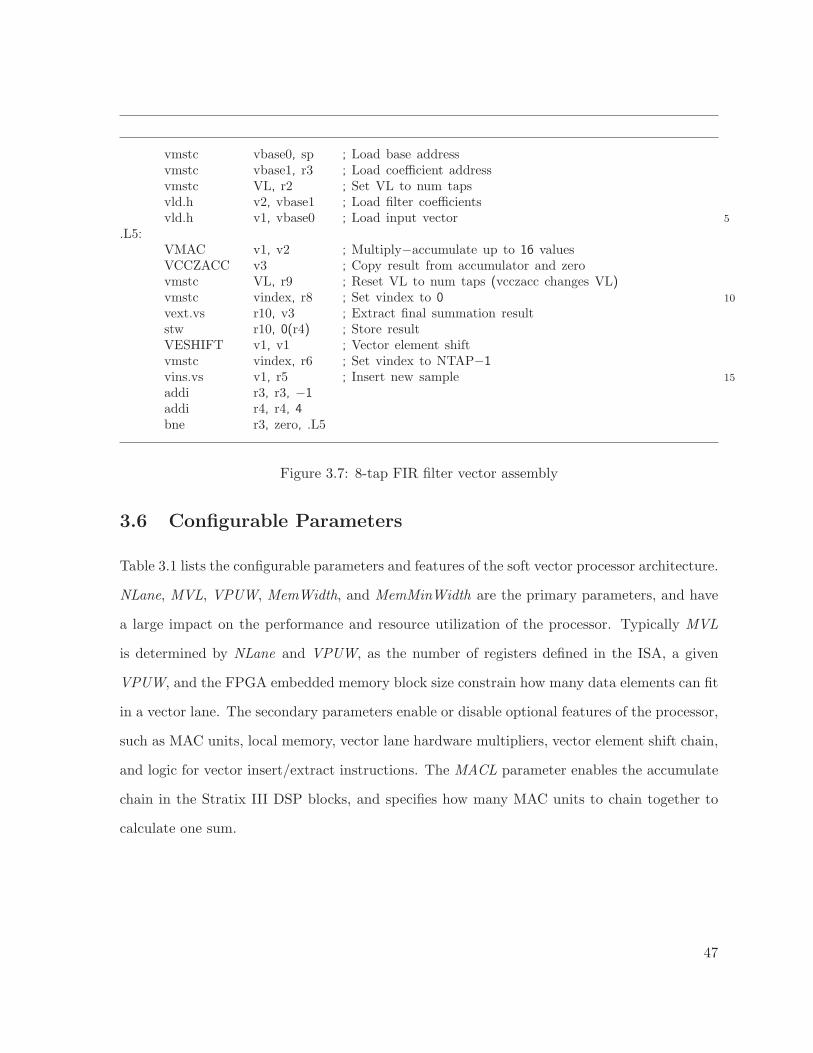
vmstc vbase0, sp ; Load base addressvmstc vbase1, r3 ; Load coefficient addressvmstc VL, r2 ; Set VL to num tapsvld.h v2, vbase1 ; Load filter coefficientsvld.h v1, vbase0 ; Load input vector 5
.L5:VMAC v1, v2 ; Multiply−accumulate up to 16 valuesVCCZACC v3 ; Copy result from accumulator and zerovmstc VL, r9 ; Reset VL to num taps (vcczacc changes VL)vmstc vindex, r8 ; Set vindex to 0 10
vext.vs r10, v3 ; Extract final summation resultstw r10, 0(r4) ; Store resultVESHIFT v1, v1 ; Vector element shiftvmstc vindex, r6 ; Set vindex to NTAP−1vins.vs v1, r5 ; Insert new sample 15
addi r3, r3, −1addi r4, r4, 4bne r3, zero, .L5
Figure 3.7: 8-tap FIR filter vector assembly
3.6 Configurable Parameters
Table 3.1 lists the configurable parameters and features of the soft vector processor architecture.
NLane, MVL, VPUW, MemWidth, and MemMinWidth are the primary parameters, and have
a large impact on the performance and resource utilization of the processor. Typically MVL
is determined by NLane and VPUW, as the number of registers defined in the ISA, a given
VPUW, and the FPGA embedded memory block size constrain how many data elements can fit
in a vector lane. The secondary parameters enable or disable optional features of the processor,
such as MAC units, local memory, vector lane hardware multipliers, vector element shift chain,
and logic for vector insert/extract instructions. The MACL parameter enables the accumulate
chain in the Stratix III DSP blocks, and specifies how many MAC units to chain together to
calculate one sum.
47
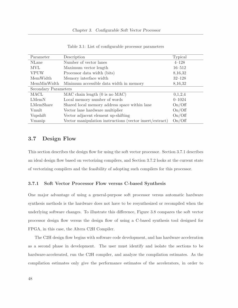
Chapter 3. Configurable Soft Vector Processor
Table 3.1: List of configurable processor parameters
Parameter Description Typical
NLane Number of vector lanes 4–128MVL Maximum vector length 16–512VPUW Processor data width (bits) 8,16,32MemWidth Memory interface width 32–128MemMinWidth Minimum accessible data width in memory 8,16,32
Secondary Parameters
MACL MAC chain length (0 is no MAC) 0,1,2,4LMemN Local memory number of words 0–1024LMemShare Shared local memory address space within lane On/OffVmult Vector lane hardware multiplier On/OffVupshift Vector adjacent element up-shifting On/OffVmanip Vector manipulation instructions (vector insert/extract) On/Off
3.7 Design Flow
This section describes the design flow for using the soft vector processor. Section 3.7.1 describes
an ideal design flow based on vectorizing compilers, and Section 3.7.2 looks at the current state
of vectorizing compilers and the feasibility of adopting such compilers for this processor.
3.7.1 Soft Vector Processor Flow versus C-based Synthesis
One major advantage of using a general-purpose soft processor versus automatic hardware
synthesis methods is the hardware does not have to be resynthesized or recompiled when the
underlying software changes. To illustrate this difference, Figure 3.8 compares the soft vector
processor design flow versus the design flow of using a C-based synthesis tool designed for
FPGA, in this case, the Altera C2H Compiler.
The C2H design flow begins with software code development, and has hardware acceleration
as a second phase in development. The user must identify and isolate the sections to be
hardware-accelerated, run the C2H compiler, and analyze the compilation estimates. As the
compilation estimates only give the performance estimates of the accelerators, in order to
48
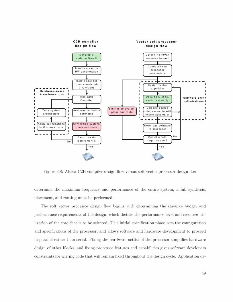
D e v e l o p C
code f o r N ios I I
I den t i f y a reas f o r
H W a c c e l e r a t i o n
I s o l a t e s e c t i o n s
t o a c c e l e r a t e i n t o
C f u n c t i o n s
R u n C 2 H
C o m p i l e r
A n a l y z e c o m p i l a t i o n
e s t i m a t e s
S y n t h e s i z e s y s t e m ,
p l a c e a n d r o u t e
R e s u l t m e e t s
r e q u i r e m e n t s ?
C 2 H c o m p i l e r
d e s i g n f l o w
A p p l y o p t i m i z a t i o n s
t o C s o u r c e c o d e
T u n e s y s t e m
a r c h i t e c t u r e
Y e s
N o
D e t e r m i n e F P G A
r e s o u r c e b u d g e t
C o n f i g u r e s o f t
p r o c e s s o r
p a r a m e t e r s
D e s i g n v e c t o r
a l g o r i t h m
D e v e l o p C c o d e ,
v e c t o r a s s e m b l y
C o m p i l e s o u r c e
c o d e , a s s e m b l e w i t h
v e c t o r a s s e m b l e r
D o w n l o a d s o f t w a r e
t o p r o c e s s o r
R e s u l t m e e t s
r e q u i r e m e n t s ?
V e c t o r s o f t p r o c e s s o r
d e s i g n f l o w
S y n t h e s i z e s y s t e m ,
p l a c e a n d r o u t e
Y e s
N o
H a r d w a r e - a w a r e
t r a n s f o r m a t i o n s
S o f t w a r e - o n l y
o p t i m i z a t i o n s
Figure 3.8: Altera C2H compiler design flow versus soft vector processor design flow
determine the maximum frequency and performance of the entire system, a full synthesis,
placement, and routing must be performed.
The soft vector processor design flow begins with determining the resource budget and
performance requirements of the design, which dictate the performance level and resource uti-
lization of the core that is to be selected. This initial specification phase sets the configuration
and specifications of the processor, and allows software and hardware development to proceed
in parallel rather than serial. Fixing the hardware netlist of the processor simplifies hardware
design of other blocks, and fixing processor features and capabilities gives software developers
constraints for writing code that will remain fixed throughout the design cycle. Application de-
49
Chapter 3. Configurable Soft Vector Processor
velopment is independent of the synthesis flow, which is only needed to determine the maximum
frequency and end performance. No resynthesis is necessary from modifications in software.
The optimization methods of the two design flows also differ. Due to the limitation of re-
quiring manual partitioning of memory, typical optimization steps with the C2H compiler are
to create more on-chip memories, reorganize data in memory by partitioning, use programming
pragmas to control connections between accelerators and memories, and manually unroll loops
to increase parallelism of the accelerator. These optimizations, especially optimizing the mem-
ory architecture, require not only a good understanding of the algorithm, but also hardware
design knowledge and thinking. On the contrary, optimizations in the soft vector processor de-
sign flow do not require any understanding of the hardware implementation of the processor or
to alter any parts of the hardware besides setting a few high level parameters according to the
software needs. Optimizing the algorithm on the software level to achieve better vectorization
is something that an average software developer can do. Hence the soft vector processor can
deliver FPGA accelerated performance to a wider software developer user base.
3.7.2 Comment on Vectorizing Compilers
The ease-of-use of the vector programming model depends greatly on the availability of a
vectorizing compiler. No vectorizing compiler was developed or used in this thesis due to time
constraints. However, vectorizing compilers exist and have been used, for example, in the past
and present Cray supercomputers. The VIRAM project, which much of this work and the soft
vector processor instruction set is based on, originally developed a compiler based on the Cray
PDGS system for vector supercomputers. The compiler for the Cell processor supports auto-
SIMDization to automatically extract SIMD parallelism and generate code for the Cell SIMD
processors. Furthermore, GCC also has an auto-vectorization feature (partially developed by
IBM) that is partially enabled and being continually developed. Therefore it should be feasible
to modify an existing vectorizing compiler for this soft vector processor.
50
Chapter 4
Results
This chapter presents performance results from benchmarking the soft vector processor, and
compares its performance to the Nios II soft processor and the Altera C2H compiler discussed in
Section 2.5.1. The chapter first describes the benchmarks and the methodology, then presents
the results and comparisons between the different systems.
4.1 Benchmark Suite
Three benchmark kernels representative of data-parallel embedded applications are chosen to
compare the performance of the different approaches. They are taken from algorithms in MPEG
encoding, image processing, and encryption. The following sections describe the operation of
the three benchmarks.
Block Matching Motion Estimation
Block matching motion estimation is used in video compression algorithms to remove temporal
redundancy within frames and allow coding systems to achieve a high compression ratio. The
algorithm divides each luma frame into blocks of size N × N , and matches each block in the
current frame with candidate blocks of the same size within a search area in the reference
frame. The best matched block has the lowest distortion among all candidate blocks, and the
displacement of the block, or the motion vector, is used to encode the video sequence. The
metric is typically sum of absolute differences (SAD), defined as:
51

Chapter 4. Results
for(l=0; l<nVERT; l++)for(k=0; k<nHORZ; k=++) {
answer = 0;for(j=0; j<16; j++)
for(i=0; i<16; i++) { 5
temp = x[l+j][k+i] − y[l+j][k+i];answer += ((temp >> 31) == 1)? (˜temp + 1) : temp;
}result[l][k] = answer;
} 10
Figure 4.1: Motion estimation C code
SAD(m, n) =N−1∑
i=0
N−1∑
j=0
|c(i, j) − s(i + m, j + n)|.
A full search block matching algorithm (FSBMA) matches the current block c to all candi-
date blocks in the reference frame s within a search range [−p, p−1], and finds the motion vector
of the block with minimum SAD among the (2p)2 search positions. Performing full search re-
quires huge computational power. For example, real time motion estimation for CIF (352×288)
30 frames per second (fps) video with [−16, +15] search range requires 9.3 giga-operations per
second (GOPS) [65]. Due to the large computational requirements and regularity of data flow,
many FSBMA hardware architectures have been developed. Figure 4.1 shows example C code
for the motion estimation kernel.
Image Median Filter
The median filter is commonly used in image processing to reduce noise in an image and is
particularly effective against impulse noise. It replaces each pixel with the median value of
surrounding pixels within a window. Figure 4.2 shows example C code for a simple median
filtering algorithm that processes an image using the median of a 5×5 image region. It operates
by performing a bubble sort, stopping early when the top half is sorted to locate the median.
52

for (i=0; i<=12; i++) {min = array[i];for (j=i; j<=24; j++) {
if (array[j] < min) {temp = min; 5
min = array[j];array[j] = temp;
}}
} 10
Figure 4.2: 5 × 5 median filter C code
AES Encryption
The 128-bit AES Encryption algorithm [66] is an encryption standard adopted by the U.S.
government. The particular implementation used here is taken from the MiBench benchmark
suite [67]. It is a block cipher, and has a fixed block size of 128 bits. Each block of data
can be logically arranged into a 4 × 4 matrix of bytes, termed the AES state. A 128-bit key
implementation, which consists of 10 encryption rounds, is used. Each round in the algorithm
consists of four steps: SubBytes, ShiftRows, MixColumns, and AddRoundKey. The first 3 steps
can be implemented efficiently on 32-bit processors using a single 1 KB lookup table. A single
round is then accomplished through four table-lookups, three byte rotations, and four EXOR
operations [68].
4.2 Benchmark Preparation
The following sections describe how the benchmarks were prepared for performance measure-
ments on the different systems. Specific steps taken to vectorize the benchmarks for the soft
vector processor, and to tune the benchmarks for the C2H compiler are also described.
53

Chapter 4. Results
4.2.1 General Methodology
The benchmarks include only the main loop section of the kernels. The median filter kernel
calculates one output pixel from the 5 × 5 window. The motion estimation kernel calculates
SAD values for each position of a [−16, +15] search range and stores the values into an array. It
makes no comparisons between the values. The AES encryption kernel computes all rounds of
encryption on 128 bits of data. The instruction and cycle counts for one intermediate round of
the 10-round algorithm are reported, as the final round is handled differently and is not within
the main loop.
As there is no vector compiler for this project, the benchmark kernels were vectorized by
embeddeding vector assembly instructions for the soft vector processor using gcc style inline
assembly, then compiled using the Nios II gcc (nios2-elf-gcc 3.4.1) with optimization O3. A
modified Nios II assembler that adds vector instruction support was used to assemble the code.
4.2.2 Benchmark Vectorization
The three kernel benchmarks were vectorized manually using a mix of assembly and C code. The
following sections describe at a high level how the kernels were vectorized, and show segments
of the vector assembly codes.
Motion Estimation
In a vector processor implementation of full search motion estimation, one of the dimensions
is handled by vectorizing (removing) the innermost loop. This vectorization step supports up
to a vector length of 16 due to the 16 × 16 pixel size of macroblocks in MPEG. With 8 lanes
and MVL of 32, two copies of the current macroblock can be matched against the search area
simultaneously, reducing the number of iterations required to process the entire search range.
To keep the innermost loop fast, only unit stride vector load instructions, which execute the
fastest, are used.
Figure 4.3 shows how the matching is accomplished using only unit stride load memory
54
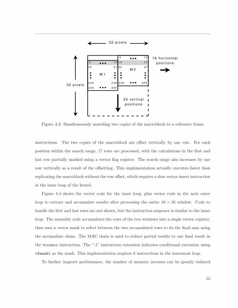
0 1 5
0 1 5
1 6 3 1
1 6 3 1 3 2 4 7
2 3 9 2 5 5
2 3 9 2 5 5
2 2 3 2 3 8
W 1
W 2
3 2 p i x e l s
3 2 p i x e l s
33 ve r t i ca l
p o s i t i o n s
1 6 h o r i z o n t a l
p o s i t i o n s
Figure 4.3: Simultaneously matching two copies of the macroblock to a reference frame
instructions. The two copies of the macroblock are offset vertically by one row. For each
position within the search range, 17 rows are processed, with the calculations in the first and
last row partially masked using a vector flag register. The search range also increases by one
row vertically as a result of the offsetting. This implementation actually executes faster than
replicating the macroblock without the row offset, which requires a slow vector insert instruction
in the inner loop of the kernel.
Figure 4.4 shows the vector code for the inner loop, plus vector code in the next outer
loop to extract and accumulate results after processing the entire 16 × 16 window. Code to
handle the first and last rows are not shown, but the instruction sequence is similar to the inner
loop. The assembly code accumulates the rows of the two windows into a single vector register,
then uses a vector mask to select between the two accumulated rows to do the final sum using
the accumulate chain. The MAC chain is used to reduce partial results to one final result in
the vcczacc instruction. The “.1” instruction extension indicates conditional execution using
vfmask1 as the mask. This implementation requires 6 instructions in the innermost loop.
To further improve performance, the number of memory accesses can be greatly reduced
55

Chapter 4. Results
vmstc vbase1, r5 ; Load x basevmstc vbase2, r6 ; Load y basevadd v5, v0, v0 ; Zero sum
.L15: ; Innermost loop over rows 5
vld.b v2, vbase1, vinc1 ; load block pixels, vinc1 = 16vld.b v3, vbase2, vinc2 ; load frame pixels, vinc2 = IMAGEWIDTHvabsdiff v4, v2, v3vadd v5, v5, v4 ; Accumulate to sumaddi r2, r2, −1 ; j++ 10
bne r2, zero, .L15 ; Loop again if (j<15)
vfld vfmask1, vbase4, vinc4 ; Load flag maskvmac.1 v6, v5 ; Accumulate across sumvcczacc v6 ; Copy from accumulator 15
vmstc VL, r9 ; Reset VL after vcczaccvext.vs r3, v6 ; Extract result to scalar core
Figure 4.4: Code segment from the motion estimation vector assembly. The code to handle thefirst and last rows of the windows are not shown.
by unrolling the loop so pixels in the floating blocks only need to be loaded once into vector
registers. To slide the window horizontally, the rows from the reference frame can be shifted
using vector element shift instead of loading the pixels repeatedly with new offsets.
Two versions of the motion estimation vector assembly are required. One is used for a 4
vector lane configuration to handle the one block, while the other is used to handle two offset
blocks with 8 or 16 vector lanes.
Image Median Filter
The median filter kernel vectorizes very nicely by exploiting outer-loop parallelism. Figure 4.5
shows how this can be done. Each strip represents one row of MVL number of pixels, and each
row is loaded into a separate vector register. The window of pixels that is being processed will
then reside in the same data element over 25 vector registers. After initial setup, the same
filtering algorithm as the scalar code can then be used. The vector processor uses masked
execution to implement conditionals, and will execute all instructions inside the conditional
56
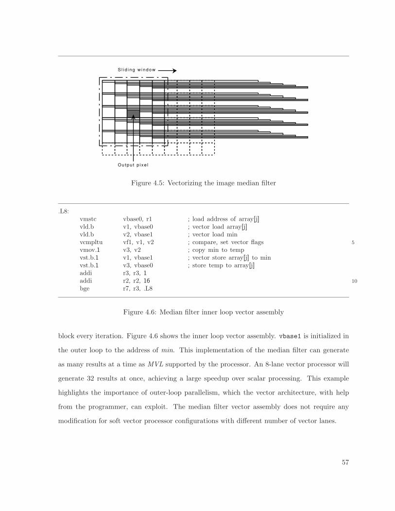
S l i d i n g w i n d o w
O u t p u t p i x e l
Figure 4.5: Vectorizing the image median filter
.L8:vmstc vbase0, r1 ; load address of array[j]vld.b v1, vbase0 ; vector load array[j]vld.b v2, vbase1 ; vector load minvcmpltu vf1, v1, v2 ; compare, set vector flags 5
vmov.1 v3, v2 ; copy min to tempvst.b.1 v1, vbase1 ; vector store array[j] to minvst.b.1 v3, vbase0 ; store temp to array[j]addi r3, r3, 1addi r2, r2, 16 10
bge r7, r3, .L8
Figure 4.6: Median filter inner loop vector assembly
block every iteration. Figure 4.6 shows the inner loop vector assembly. vbase1 is initialized in
the outer loop to the address of min. This implementation of the median filter can generate
as many results at a time as MVL supported by the processor. An 8-lane vector processor will
generate 32 results at once, achieving a large speedup over scalar processing. This example
highlights the importance of outer-loop parallelism, which the vector architecture, with help
from the programmer, can exploit. The median filter vector assembly does not require any
modification for soft vector processor configurations with different number of vector lanes.
57
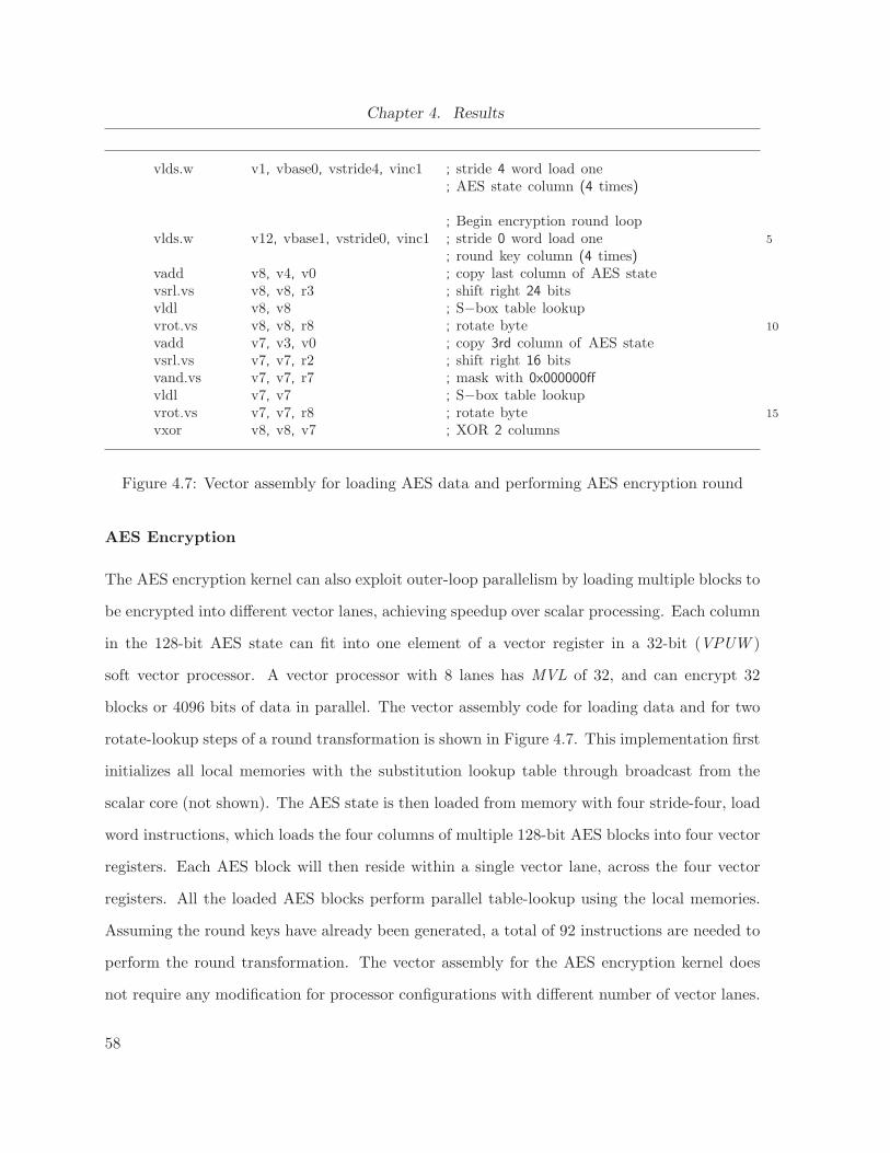
Chapter 4. Results
vlds.w v1, vbase0, vstride4, vinc1 ; stride 4 word load one; AES state column (4 times)
; Begin encryption round loopvlds.w v12, vbase1, vstride0, vinc1 ; stride 0 word load one 5
; round key column (4 times)vadd v8, v4, v0 ; copy last column of AES statevsrl.vs v8, v8, r3 ; shift right 24 bitsvldl v8, v8 ; S−box table lookupvrot.vs v8, v8, r8 ; rotate byte 10
vadd v7, v3, v0 ; copy 3rd column of AES statevsrl.vs v7, v7, r2 ; shift right 16 bitsvand.vs v7, v7, r7 ; mask with 0x000000ffvldl v7, v7 ; S−box table lookupvrot.vs v7, v7, r8 ; rotate byte 15
vxor v8, v8, v7 ; XOR 2 columns
Figure 4.7: Vector assembly for loading AES data and performing AES encryption round
AES Encryption
The AES encryption kernel can also exploit outer-loop parallelism by loading multiple blocks to
be encrypted into different vector lanes, achieving speedup over scalar processing. Each column
in the 128-bit AES state can fit into one element of a vector register in a 32-bit (VPUW )
soft vector processor. A vector processor with 8 lanes has MVL of 32, and can encrypt 32
blocks or 4096 bits of data in parallel. The vector assembly code for loading data and for two
rotate-lookup steps of a round transformation is shown in Figure 4.7. This implementation first
initializes all local memories with the substitution lookup table through broadcast from the
scalar core (not shown). The AES state is then loaded from memory with four stride-four, load
word instructions, which loads the four columns of multiple 128-bit AES blocks into four vector
registers. Each AES block will then reside within a single vector lane, across the four vector
registers. All the loaded AES blocks perform parallel table-lookup using the local memories.
Assuming the round keys have already been generated, a total of 92 instructions are needed to
perform the round transformation. The vector assembly for the AES encryption kernel does
not require any modification for processor configurations with different number of vector lanes.
58

4.2.3 Benchmark Tuning for C2H Compiler
The C2H compiler generates only a single hardware accelerator for a given C function. The
only built-in options for customization are pragmas for controlling interrupt behaviour and
generation of master ports to access memory. One set of accelerators were generated by directly
compiling the kernels with as little modification to the C code as possible. These are named
the “push-button” C2H accelerators. To compare the scalability of C2H-generated accelerators
versus the soft vector processor, the C source code of the benchmark kernels were manually
modified to generate accelerators with different performance and resource tradeoff for a second
set of results. Vector processing concepts were applied to the C code by unrolling loops and
declaring additional variables to calculate multiple results in parallel.
The median filter kernel did not require any additional optimization besides unrolling.
For the motion estimation kernel, the horizontal-move outer loop was moved inside and
unrolled, resulting in one pixel of the moving block being compared to up to 32 possible hori-
zontal locations in parallel, creating 32 accumulators for the SAD operation. One pixel datum is
loaded from memory to register once, then re-used 32 times by the 32 accumulators. Hardware
knowledge is needed to know that the 32 accumulators will be inferred to hold the intermediate
results. The manual unrolling also created very hard-to-maintain C code.
The AES encryption kernel requires four table lookup operations for the four columns in the
AES state. These operations were optimized to be performed in parallel by instantiating four
separate 256-entry, 32-bit memories local to the accelerator. This was not done automatically
by the compiler as the lookup tables were initially declared as global variables, which the
compiler automatically placed in main memory. The AES engine was further replicated to
increase performance at the expense of increased resources. The effects of these optimizations
on performance will be shown in Section 4.4.3.
59
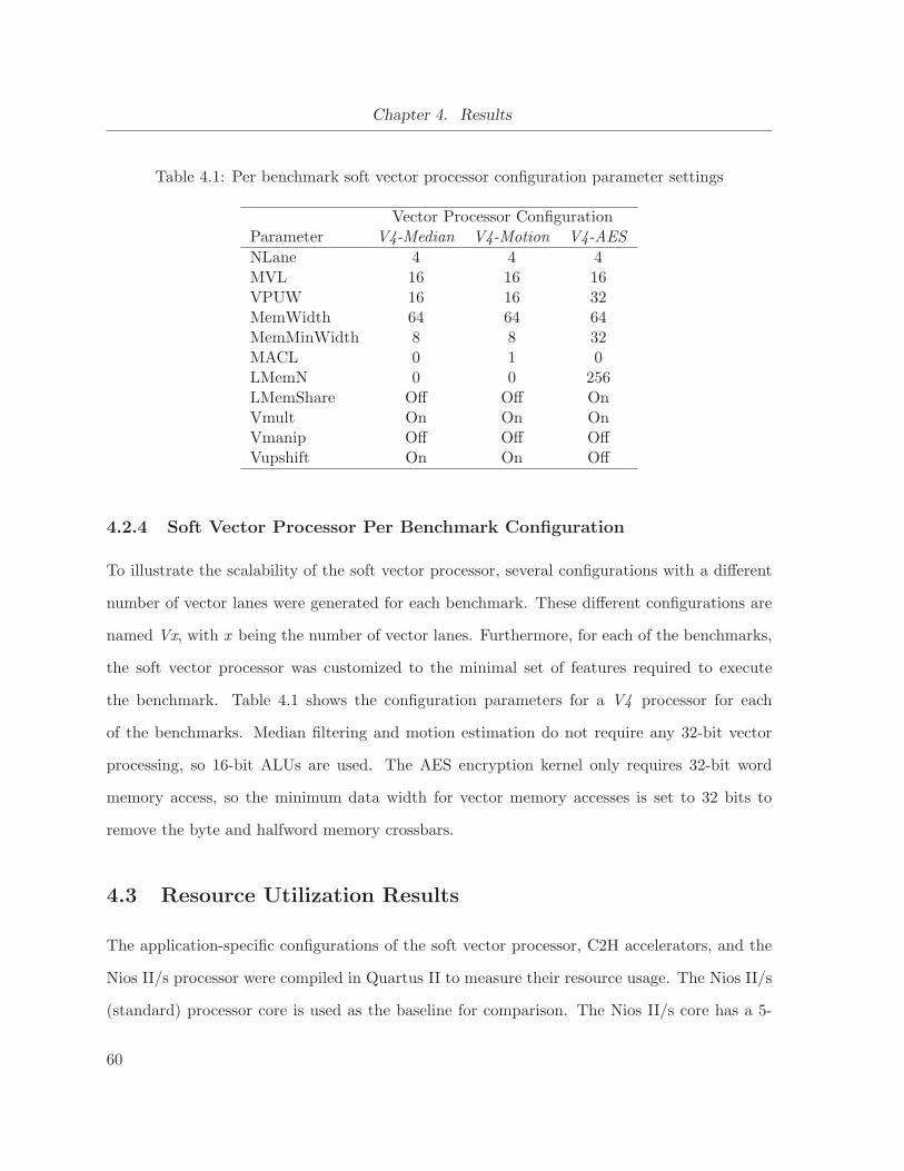
Chapter 4. Results
Table 4.1: Per benchmark soft vector processor configuration parameter settings
Vector Processor ConfigurationParameter V4-Median V4-Motion V4-AES
NLane 4 4 4MVL 16 16 16VPUW 16 16 32MemWidth 64 64 64MemMinWidth 8 8 32MACL 0 1 0LMemN 0 0 256LMemShare Off Off OnVmult On On OnVmanip Off Off OffVupshift On On Off
4.2.4 Soft Vector Processor Per Benchmark Configuration
To illustrate the scalability of the soft vector processor, several configurations with a different
number of vector lanes were generated for each benchmark. These different configurations are
named Vx, with x being the number of vector lanes. Furthermore, for each of the benchmarks,
the soft vector processor was customized to the minimal set of features required to execute
the benchmark. Table 4.1 shows the configuration parameters for a V4 processor for each
of the benchmarks. Median filtering and motion estimation do not require any 32-bit vector
processing, so 16-bit ALUs are used. The AES encryption kernel only requires 32-bit word
memory access, so the minimum data width for vector memory accesses is set to 32 bits to
remove the byte and halfword memory crossbars.
4.3 Resource Utilization Results
The application-specific configurations of the soft vector processor, C2H accelerators, and the
Nios II/s processor were compiled in Quartus II to measure their resource usage. The Nios II/s
(standard) processor core is used as the baseline for comparison. The Nios II/s core has a 5-
60
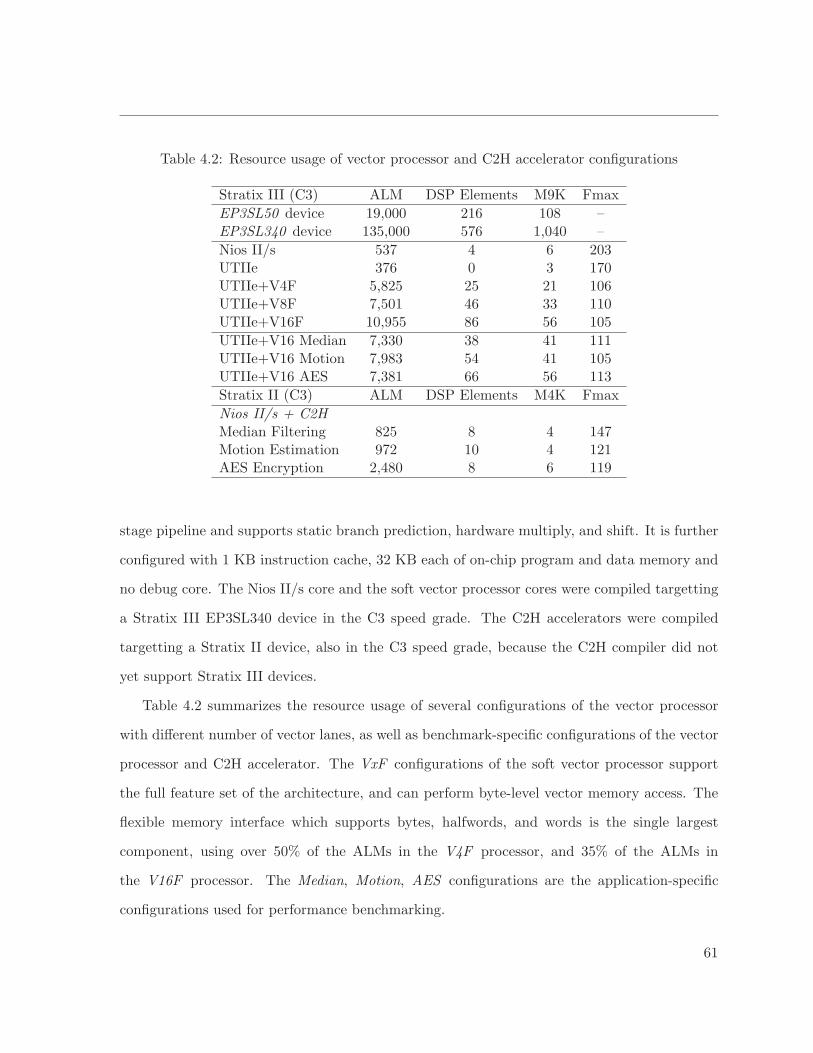
Table 4.2: Resource usage of vector processor and C2H accelerator configurations
Stratix III (C3) ALM DSP Elements M9K Fmax
EP3SL50 device 19,000 216 108 –EP3SL340 device 135,000 576 1,040 –
Nios II/s 537 4 6 203UTIIe 376 0 3 170UTIIe+V4F 5,825 25 21 106UTIIe+V8F 7,501 46 33 110UTIIe+V16F 10,955 86 56 105
UTIIe+V16 Median 7,330 38 41 111UTIIe+V16 Motion 7,983 54 41 105UTIIe+V16 AES 7,381 66 56 113
Stratix II (C3) ALM DSP Elements M4K Fmax
Nios II/s + C2HMedian Filtering 825 8 4 147Motion Estimation 972 10 4 121AES Encryption 2,480 8 6 119
stage pipeline and supports static branch prediction, hardware multiply, and shift. It is further
configured with 1 KB instruction cache, 32 KB each of on-chip program and data memory and
no debug core. The Nios II/s core and the soft vector processor cores were compiled targetting
a Stratix III EP3SL340 device in the C3 speed grade. The C2H accelerators were compiled
targetting a Stratix II device, also in the C3 speed grade, because the C2H compiler did not
yet support Stratix III devices.
Table 4.2 summarizes the resource usage of several configurations of the vector processor
with different number of vector lanes, as well as benchmark-specific configurations of the vector
processor and C2H accelerator. The VxF configurations of the soft vector processor support
the full feature set of the architecture, and can perform byte-level vector memory access. The
flexible memory interface which supports bytes, halfwords, and words is the single largest
component, using over 50% of the ALMs in the V4F processor, and 35% of the ALMs in
the V16F processor. The Median, Motion, AES configurations are the application-specific
configurations used for performance benchmarking.
61
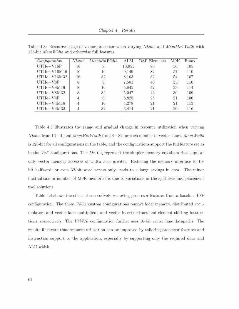
Chapter 4. Results
Table 4.3: Resource usage of vector processor when varying NLane and MemMinWidth with128-bit MemWidth and otherwise full features
Configuration NLane MemMinWidth ALM DSP Elements M9K Fmax
UTIIe+V16F 16 8 10,955 86 56 105UTIIe+V16M16 16 16 9,149 82 57 110UTIIe+V16M32 16 32 8,163 82 54 107UTIIe+V8F 8 8 7,501 46 33 110UTIIe+V8M16 8 16 5,845 42 33 114UTIIe+V8M32 8 32 5,047 42 30 109UTIIe+V4F 4 8 5,825 25 21 106UTIIe+V4M16 4 16 4,278 21 21 113UTIIe+V4M32 4 32 3,414 21 20 116
Table 4.3 illustrates the range and gradual change in resource utilization when varying
NLane from 16 – 4, and MemMinWidth from 8 – 32 for each number of vector lanes. MemWidth
is 128-bit for all configurations in the table, and the configurations support the full feature set as
in the VxF configurations. The Mx tag represent the simpler memory crossbars that support
only vector memory accesses of width x or greater. Reducing the memory interface to 16-
bit halfword, or even 32-bit word access only, leads to a large savings in area. The minor
fluctuations in number of M9K memories is due to variations in the synthesis and placement
tool solutions.
Table 4.4 shows the effect of successively removing processor features from a baseline V8F
configuration. The three V8Cx custom configurations remove local memory, distributed accu-
mulators and vector lane multipliers, and vector insert/extract and element shifting instruc-
tions, respectively. The V8W16 configuration further uses 16-bit vector lane datapaths. The
results illustrate that resource utilization can be improved by tailoring processor features and
instruction support to the application, especially by supporting only the required data and
ALU width.
62

Table 4.4: Resource utilization from varying secondary processor parameters
Vector Processor Configuration (UTIIe+)Resource V8F V8C1 V8C2 V8C3 V8W16
ALM 7,501 7,505 6,911 6,688 5,376DSP Elements 46 46 6 6 6M9K 33 25 25 25 25Fmax 110 105 107 113 114
Parameter Values
NLane 8 8 8 8 8MVL 32 32 32 32 32VPUW 32 32 32 32 16MemWidth 128 128 128 128 128MemMinWidth 8 8 8 8 8MACL 2 2 0 0 0LMemN 256 0 0 0 0LMemShare On Off Off Off OffVmult On On Off Off OffVmanip On On On Off OffVupshift On On On Off Off
4.4 Performance Results
The following sections present performance results of the soft vector processor, and compares
them to the Nios II/s processor and the C2H compiler. Performance models were used to
estimate the performance of each of the systems, with two models for the soft vector processor.
The performance models will be described in the following sections together with the results.
Execution time is used as the metric to compare the different performance models. It is
estimated from instruction count, clock cycle count, and operating frequency. Fmax estimates
are obtained by compiling the systems in Quartus II 7.2 targetting a EP3SL340 device, and
running the TimeQuest timing analyzer in single-corner mode.
63

Chapter 4. Results
4.4.1 Performance Models
Four performance models for the Nios II, soft vector processor, and C2H compiler are compared
using execution time for the three benchmark kernels. The four models are Ideal Nios Model,
soft vector processor RTL Model, Ideal Vector Model, and C2H Model.
Ideal Nios Model
The Ideal Nios Model simulates ideal execution conditions for a Nios II processor, and is used
as the baseline for comparison. The model executes all Nios II assembly instructions in a
single cycle; this presumes perfect caching and branch prediction. Execution time is calculated
by counting the number of cycles needed to execute the assembly code, and dividing by the
processor maximum frequency.
RTL Model
The RTL model measures performance of the soft vector processor by performing a cycle-
by-cycle functional simulation in ModelSim of the processor RTL description executing the
benchmarks kernels. The RTL implementation of the soft vector processor uses the UTIIe,
which is a multicycle processor, as a scalar unit. Each scalar instruction takes 6 cycles, with
additional cycles needed for shift instructions. The performance of a multicycle scalar processor
is significantly worse than a fully pipelined scalar processor such as the real Nios II. As a result,
the performance of the RTL model is highly limited by the use of the UTIIe core. Single cycle
memory access is also assumed for the functional simulation, which is realistic for accessing
on-chip memories on the FPGA.
Ideal Vector Model
The Ideal Vector Model is used to estimate the potential performance of the soft vector processor
with a fully pipelined scalar unit. The Ideal Vector Model incorporates the Ideal Nios Model
64

Table 4.5: Ideal vector performance model
Instruction Class Instruction Cycles
Scalar instructions 1Vector non-memory ⌈V L/NLane⌉Vector local memory ⌈V L/NLane⌉Vector memory store ⌈V L/NLane⌉Vector memory load 2 + ⌈V L/min(NLane, MaxElem)⌉ + ⌈V L/NLane⌉
MaxElem = MemWidth/MemDataWidth
MemDataWidth is the data width of the particular vector memory access
for scalar instructions (scalar instructions execute in a single cycle). Vector instructions are
separated into different classes, each taking a different number of cycles. Table 4.5 shows the
number of cycles needed for each vector instruction class. Memory store instructions take
the same number of cycles as non-memory instructions due to write buffering. The first non-
constant term in memory load cycles models the number cycles needed to transfer data from
memory to the load buffer. MaxElem is the maximum number of data elements that can be
transferred per cycle through the MemWidth-bit memory interface. The second term models
transferring data from load buffer to the vector register file. Single cycle memory accesses is
again assumed.
Performance of the Ideal Vector Model is calculated by manually counting the number of
assembly instructions executed, then multiplying the instruction count of different instruction
classes by the cycle per instruction of the instruction class to calculate the total cycle count.
Execution time is then calculated by dividing the cycle count by the maximum frequency.
The Ideal Vector Model is optimistic in that pipeline execution and memory accesses are
ideal. No pipeline interlocks due to dependent instructions are modeled in the scalar or vector
core. However, the Ideal Vector Model is also pessimistic in one aspect because it does not
model the concurrent execution of scalar, vector arithmetic, and vector memory instructions
that is accounted for in the RTL model.
65

Chapter 4. Results
C2H Model
The C2H model simulates performance of the C2H accelerators in a SOPC system built with
the Altera SOPC Builder. Execution times of the accelerators is calculated for the main loop
only from loop latency and cycles per loop iteration (CPLI) given in the C2H compilation
performance report as well as the Fmax calculated by Quartus II.
Performance Model Usage
No board-level measurement results are presented in this thesis because a Stratix III-based
development board (DE3 development board) was not available to test the processor at the time
of writing. Also, two different performance models of the soft vector processor are presented
because the RTL model alone is severely limited by the performance of the UTIIe and is not
indicative of speedups that can be obtained with a fully pipelined scalar unit.
4.4.2 RTL Model Performance
Table 4.6 shows the simulated performance of the soft vector processor on the three benchmarks
measured by instruction count and clock cycle count. The clock cycle count and Fmax are used
to compute speedup over the baseline Ideal Nios Model. All vector configurations show speedup
over the baseline, where greater performance is obtained when more vector lanes are used. The
instruction count and clock cycle per result decreases for median filtering and AES encryption
as more vector lanes are added because more results are computed in parallel. In particular,
the fractional instruction counts for AES encryption results from dividing the total instructions
by the number of blocks encrypted in parallel. For the motion estimation kernel, instruction
count changes from V4 to V8 because the assembly source was modified to handle two SAD
calculations in parallel, but no further modification was necessary for V16. Vector length is 16
for V4 and 32 for both V8 and V16. With 16 vector lanes, V16 can process a fixed 32 length
vector in fewer cycles, yielding a smaller cycle count.
Figure 4.8 plots speedup of the soft vector processor, comparing the RTL Model to the Ideal
66
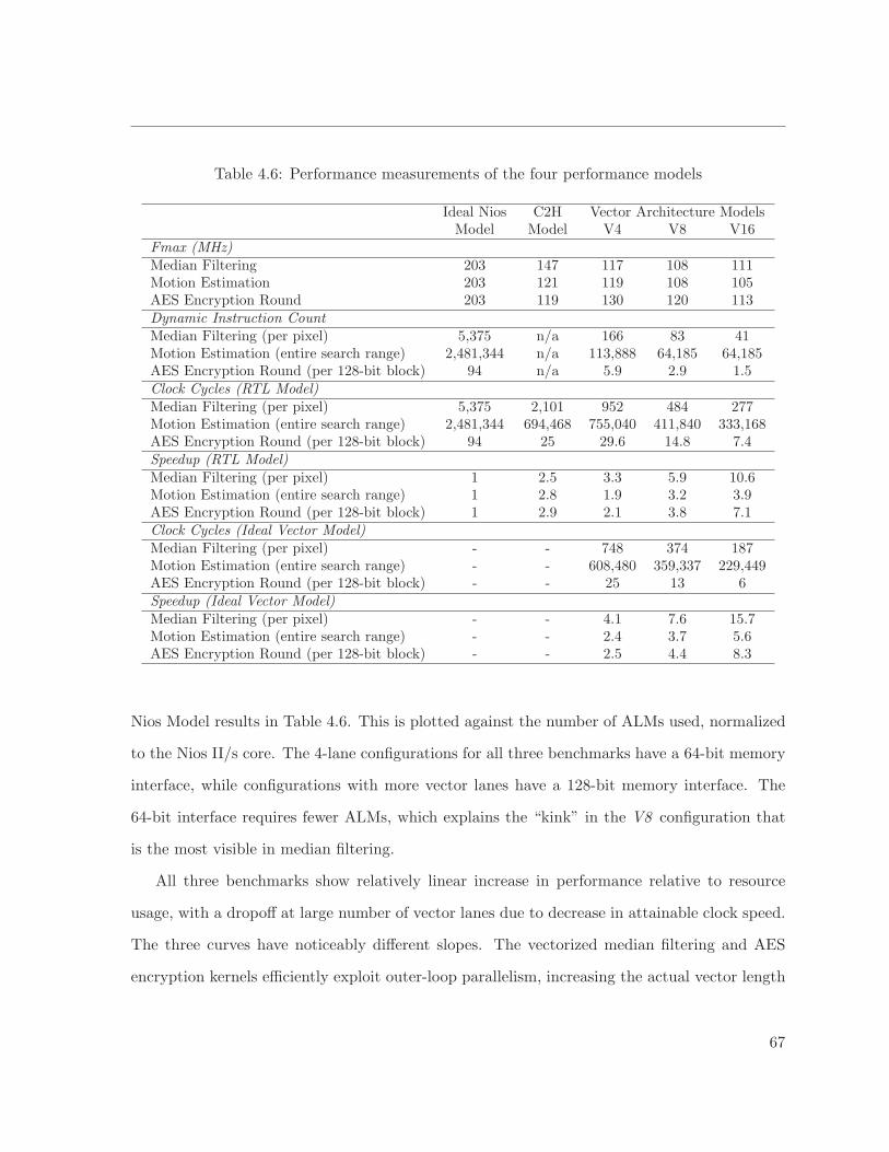
Table 4.6: Performance measurements of the four performance models
Ideal Nios C2H Vector Architecture ModelsModel Model V4 V8 V16
Fmax (MHz)Median Filtering 203 147 117 108 111Motion Estimation 203 121 119 108 105AES Encryption Round 203 119 130 120 113Dynamic Instruction CountMedian Filtering (per pixel) 5,375 n/a 166 83 41Motion Estimation (entire search range) 2,481,344 n/a 113,888 64,185 64,185AES Encryption Round (per 128-bit block) 94 n/a 5.9 2.9 1.5Clock Cycles (RTL Model)Median Filtering (per pixel) 5,375 2,101 952 484 277Motion Estimation (entire search range) 2,481,344 694,468 755,040 411,840 333,168AES Encryption Round (per 128-bit block) 94 25 29.6 14.8 7.4Speedup (RTL Model)Median Filtering (per pixel) 1 2.5 3.3 5.9 10.6Motion Estimation (entire search range) 1 2.8 1.9 3.2 3.9AES Encryption Round (per 128-bit block) 1 2.9 2.1 3.8 7.1Clock Cycles (Ideal Vector Model)Median Filtering (per pixel) - - 748 374 187Motion Estimation (entire search range) - - 608,480 359,337 229,449AES Encryption Round (per 128-bit block) - - 25 13 6Speedup (Ideal Vector Model)Median Filtering (per pixel) - - 4.1 7.6 15.7Motion Estimation (entire search range) - - 2.4 3.7 5.6AES Encryption Round (per 128-bit block) - - 2.5 4.4 8.3
Nios Model results in Table 4.6. This is plotted against the number of ALMs used, normalized
to the Nios II/s core. The 4-lane configurations for all three benchmarks have a 64-bit memory
interface, while configurations with more vector lanes have a 128-bit memory interface. The
64-bit interface requires fewer ALMs, which explains the “kink” in the V8 configuration that
is the most visible in median filtering.
All three benchmarks show relatively linear increase in performance relative to resource
usage, with a dropoff at large number of vector lanes due to decrease in attainable clock speed.
The three curves have noticeably different slopes. The vectorized median filtering and AES
encryption kernels efficiently exploit outer-loop parallelism, increasing the actual vector length
67
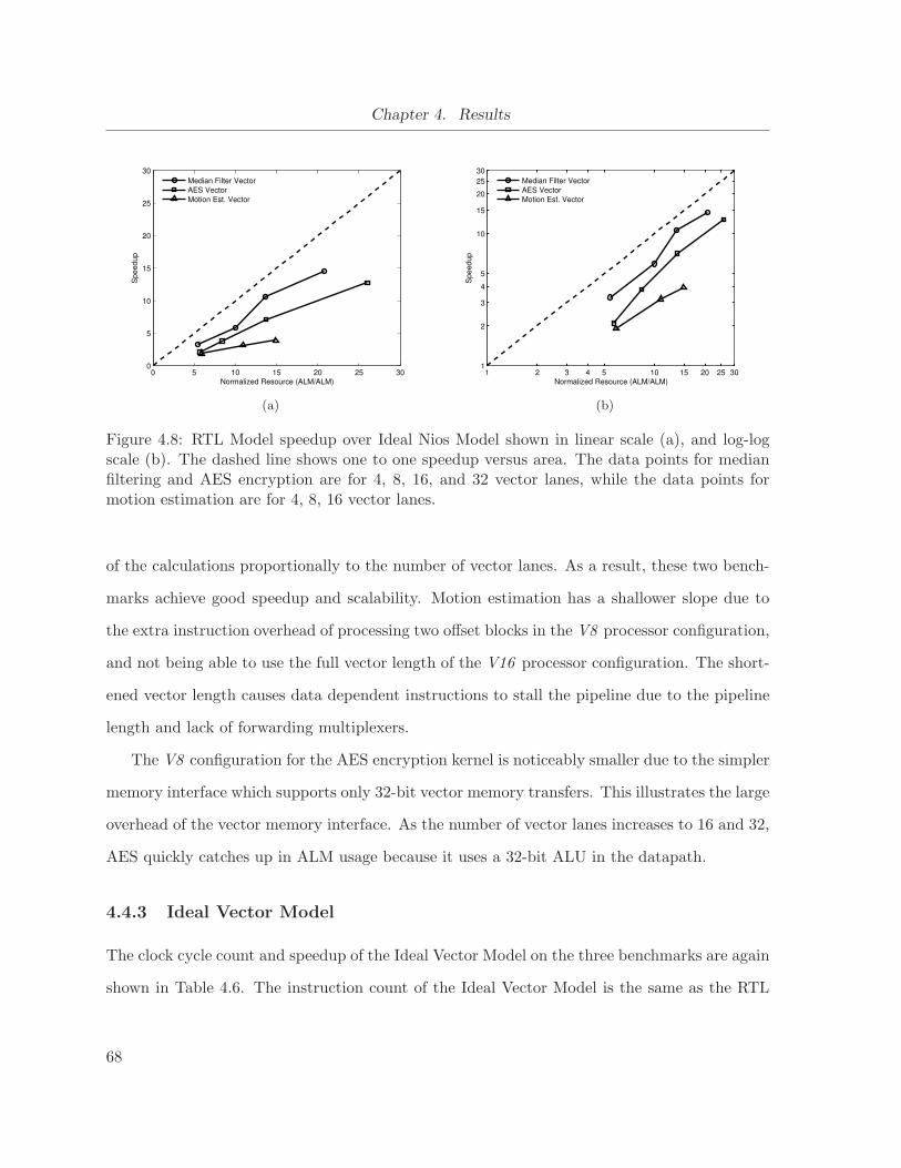
Chapter 4. Results
0 5 10 15 20 25 300
5
10
15
20
25
30
Normalized Resource (ALM/ALM)
Sp
ee
du
p
Median Filter Vector
AES Vector
Motion Est. Vector
(a)
1 2 3 4 5 10 15 20 25 301
2
3
4
5
10
15
20
25
30
Normalized Resource (ALM/ALM)
Sp
ee
du
p
Median Filter Vector
AES Vector
Motion Est. Vector
(b)
Figure 4.8: RTL Model speedup over Ideal Nios Model shown in linear scale (a), and log-logscale (b). The dashed line shows one to one speedup versus area. The data points for medianfiltering and AES encryption are for 4, 8, 16, and 32 vector lanes, while the data points formotion estimation are for 4, 8, 16 vector lanes.
of the calculations proportionally to the number of vector lanes. As a result, these two bench-
marks achieve good speedup and scalability. Motion estimation has a shallower slope due to
the extra instruction overhead of processing two offset blocks in the V8 processor configuration,
and not being able to use the full vector length of the V16 processor configuration. The short-
ened vector length causes data dependent instructions to stall the pipeline due to the pipeline
length and lack of forwarding multiplexers.
The V8 configuration for the AES encryption kernel is noticeably smaller due to the simpler
memory interface which supports only 32-bit vector memory transfers. This illustrates the large
overhead of the vector memory interface. As the number of vector lanes increases to 16 and 32,
AES quickly catches up in ALM usage because it uses a 32-bit ALU in the datapath.
4.4.3 Ideal Vector Model
The clock cycle count and speedup of the Ideal Vector Model on the three benchmarks are again
shown in Table 4.6. The instruction count of the Ideal Vector Model is the same as the RTL
68
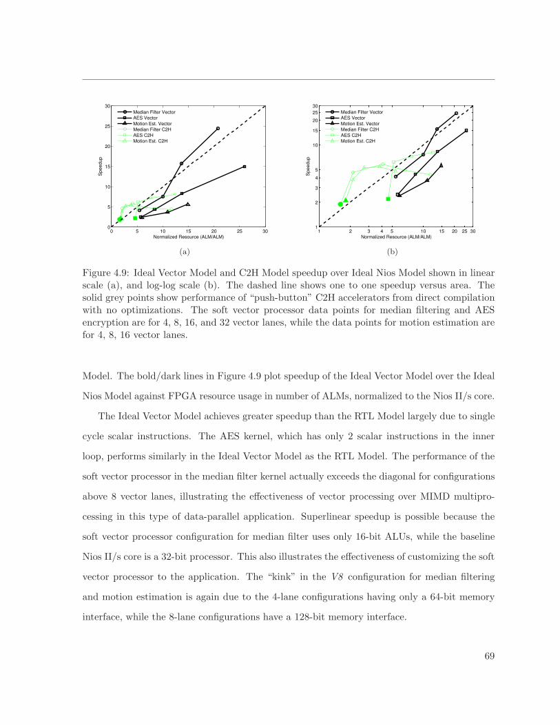
0 5 10 15 20 25 300
5
10
15
20
25
30
Normalized Resource (ALM/ALM)
Sp
ee
du
p
Median Filter Vector
AES Vector
Motion Est. Vector
Median Filter C2H
AES C2H
Motion Est. C2H
(a)
1 2 3 4 5 10 15 20 25 301
2
3
4
5
10
15
20
25
30
Normalized Resource (ALM/ALM)
Sp
ee
du
p
Median Filter Vector
AES Vector
Motion Est. Vector
Median Filter C2H
AES C2H
Motion Est. C2H
(b)
Figure 4.9: Ideal Vector Model and C2H Model speedup over Ideal Nios Model shown in linearscale (a), and log-log scale (b). The dashed line shows one to one speedup versus area. Thesolid grey points show performance of “push-button” C2H accelerators from direct compilationwith no optimizations. The soft vector processor data points for median filtering and AESencryption are for 4, 8, 16, and 32 vector lanes, while the data points for motion estimation arefor 4, 8, 16 vector lanes.
Model. The bold/dark lines in Figure 4.9 plot speedup of the Ideal Vector Model over the Ideal
Nios Model against FPGA resource usage in number of ALMs, normalized to the Nios II/s core.
The Ideal Vector Model achieves greater speedup than the RTL Model largely due to single
cycle scalar instructions. The AES kernel, which has only 2 scalar instructions in the inner
loop, performs similarly in the Ideal Vector Model as the RTL Model. The performance of the
soft vector processor in the median filter kernel actually exceeds the diagonal for configurations
above 8 vector lanes, illustrating the effectiveness of vector processing over MIMD multipro-
cessing in this type of data-parallel application. Superlinear speedup is possible because the
soft vector processor configuration for median filter uses only 16-bit ALUs, while the baseline
Nios II/s core is a 32-bit processor. This also illustrates the effectiveness of customizing the soft
vector processor to the application. The “kink” in the V8 configuration for median filtering
and motion estimation is again due to the 4-lane configurations having only a 64-bit memory
interface, while the 8-lane configurations have a 128-bit memory interface.
69
Chapter 4. Results
4.4.4 C2H Accelerator Results
The C2H accelerator performance numbers are also summarized in Table 4.6, measured by
the same clock cycle count and speedup over the Ideal Nios Model. These numbers represent
results achieveable by “push-button” acceleration with the compiler, with no modification to
the original C code4. These results are shown by the solid grey dots in Figure 4.9. Performance
of the “push-button” C2H accelerators are similar to those of the V4 processor configurations,
but they do not match those of the larger vector processor configurations.
The thin/gray lines in Figure 4.9 show the performance improvement trend when the C2H
accelerators are scaled and optimized as described in Section 4.2.3. Applying vector processing
concepts and loop unrolling makes it possible to increase C2H performance at the expense of
increased resources.
Although performance increases, notice that it also saturates in all C2H accelerators as
memory access becomes the bottleneck. This occurs in the median filter kernel when the loop
is unrolled 64 times to find 64 medians in parallel, because each iteration requires 64 new data
items to be read and 64 new values to be written back. For motion estimation, comparing a
single pixel to 32 copies of the window and reading from 32 possible horizontal locations creates
a memory bottleneck.
For AES encryption, memory saturation was initially avoided by adding 4 memory blocks
for the 256-entry, 32-bit lookup tables in the Nios II system as a hardware-level optimization.
This single change achieved a large speedup over the “push-button” result, indicated by the
large jump of the second data point on the curve. Further replicating the AES engine up to four
times created contention at the lookup table memories. Resolving this bottleneck would require
a dedicated copy of all tables for each engine. In all three benchmarks, additional performance
from C2H accelerators is possible by making changes to the Nios II memory system.
4Stratix II was used for the C2H estimates because Quartus II does not yet support C2H hardware acceleratorsfor Stratix III-based designs. We expect results to be similar to Stratix II due to the similar ALM architecture.
70

4.4.5 Vector versus C2H
Figure 4.9 illustrated the difference in scalability of the soft vector processor and C2H accel-
erators. By scaling the number of vector lanes, the soft vector processor simultaneously scales
the vector register file bandwidth. And since most operations inside inner loops of kernels read
from and write to vector registers, increasing the register file bandwidth allows more data ele-
ments to be accessed and processed in parallel each cycle, increasing performance. The vector
programming model abstracts the scalable architecture, providing the same unified memory
system to the user across different configurations. This abstraction also allows the user to take
advantage of scalable performance with zero hardware design effort.
It is also possible to scale bandwidth to internal register states of the C2H accelerators, and
in fact that was already done by manually unrolling loops and declaring additional variables.
However, the C2H accelerators are not able to efficiently gather data from main memory when
bandwidth of the internal state registers is increased, leading to performance saturation. The
flexible vector memory interface of the soft vector processor did accomplish this.
The soft vector processor is an application-independent accelerator, where a single con-
figuration of the processor could have been used to accelerate all three benchmarks (albeit,
for slightly lower performance), or multiple portions of the application. Synthesized hardware
accelerator tools will require separate accelerators for different sections.
As a rough comparison of effort, it took approximately 3 days to learn to use the C2H com-
piler, modify the three benchmark kernels so they compile, and apply the simple loop unrolling
software optimization. It took another full day to apply the single hardware optimization for
the AES benchmark of adding the additional memories. With the vector processor, it took 2
days to design the initial vectorized algorithms and assembly code for all three kernels. The
rich instruction set of the processor allows many possible ways to vectorize an algorithm to
tune performance using software skills. The vector assembly code of the AES encryption and
motion estimation kernels have actually each been rewritten once using a different vectorization
method during the course of software development. Each iteration of designing and coding the
71

Chapter 4. Results
vector assembly took less than half a day.
72

Chapter 5
Conclusions and Future Work
As the performance requirements and complexity of embedded systems continue to increase,
designers need a high performance platform that reduces development effort and time-to-market.
This thesis applies vector processing to soft processor systems on FPGAs to improve their
performance in data-parallel embedded workloads. Previous work in vector microprocessors
[6, 12] have demonstrated the feasibility and advantages of accelerating embedded applications
with vector processing. The soft vector processor provides the same advantages, with the added
benefit of soft processor configurability. Compared to other soft processor accelerator solutions,
a soft vector processor allows application acceleration with purely software development effort
and requires no hardware knowledge. The application-independent architecture helps separate
hardware and software development early in the design flow.
The soft vector processor leverages the configurability of soft processors and FPGAs to
provide user-selectable performance and resource tradeoff, and application-specific tuning of
the instruction set and processor features. It incorporates a range of configurable parameters
that can significantly impact the area and performance of the processor, the most important
of which are NLane (the number of vector lanes; also determines the maximum vector length
supported by the processor), and VPUW (the vector lane ALU width). The processor also
introduces a flexible and configurable vector memory interface to a single memory bank that
supports unit stride, constant stride, and indexed vector memory accesses. The width of the
memory interface is configurable, and the interface can be configured to only support a minimum
data width of 8-bit bytes, 16-bit halfwords, or 32-bit words for vector memory accesses through
the MemMinWidth parameter. Setting the minimum data width to 32-bit words, for example,
73

Chapter 5. Conclusions and Future Work
removes logic for accessing smaller data widths, reducing the size of the memory crossbars and
results in a large savings in area. This additional level of configurability enlarges the design
space, allowing the designer to make larger tradeoffs than other soft processor solutions.
The soft vector processor is shown in this thesis to outperform an ideal Nios II and the
Altera C2H compiler. Functional simulation of the RTL model with a multicycle scalar unit
achieved speedup of up to 11× for 16 vector lanes over an ideal Nios II processor model. The
ideal vector model that incorporates a fully pipelined scalar unit estimates speedup of up to 24×
for 32 vector lanes, versus up to 8× for C2H accelerators. By customizing the soft processor
to the benchmarks, area savings of up to 33% was achieved for 16 vector lanes compared to a
generic configuration of the processor that supported the full range of features.
The instruction set of the soft vector processor is adapted from the VIRAM instruction
set. The architecture is tailored to the Stratix III FPGA, and introduces novel features to take
advantage of the embedded memory blocks and hardwired DSP blocks. The datapath uses a
partitioned register file to reduce complexity of the vector register file, and executes instructions
in a novel hybrid vector-SIMD fashion to speed instruction execution. MAC units are added
for accumulating multi-dimensional data and vector sum reduction. Together with new vector
adjacent element shift and vector absolute difference instructions, they significantly reduce
the execution time of the motion estimation kernel over an implementation with the VIRAM
instruction set. A vector lane local memory is also introduced for table lookup operations within
a vector lane, and is used by the AES encryption kernel.
A soft vector processor has advantages over many currently available soft processor acceler-
ator tools, and is most suitable when rapid development time is required, or when a hardware
designer is not available, or when several different applications must share a single accelerator.
74

5.1 Future Work
This thesis has described a prototype of a soft vector processor targeted to FPGAs, and illus-
trated its advantages and potential performance. The implementation details of the soft vector
processor prototype can be optimized and improved in many ways. However, the next sections
will focus on possible major improvements to the processor architecture that can potentially
have a significant impact on performance or area usage.
Pipelined and Multiple-Issue Scalar Unit
Performance of a vector processor depends significantly on perfomance of the scalar unit on non-
vectorizable portions of the application due to Amdahl’s Law. Implementing a fully-pipelined
scalar unit in the soft vector processor will boost the performance of the current processor
prototype tremendously, as shown by the results in this thesis, and would be the logical next
step in improving the processor.
Even with a fully-pipelined scalar unit, the soft vector processor would still be limited by
the single instruction fetch from sharing a common fetch stage between the scalar and vector
units. As the scalar and vector units already have separate decode logic, a multiple instruction
fetch and issue core can be considered to further improve pipeline utilization. To avoid the
complexity of superscalar processors, the compiler can statically arrange the code (similar to
VLIW techniques) such that vector instructions always enter the vector issue pipeline, and
scalar instructions always enter the scalar pipeline.
Addition of Caches
Modern processors rely on multiple levels of cache to bridge the gap between processor clock
speed and speed of external memory. Instruction and data caches can be implemented for the
scalar unit of the soft vector processor in the same manner as other RISC processor cores.
Synchronization mechanisms will be required to keep the data cache of the scalar unit in sync
75
Chapter 5. Conclusions and Future Work
with vector memory accesses. Traditional vector processors like the NEC SX-7 [69] do not
employ data caches for the vector core, and instead hide memory latency by overlapping vector
execution and memory fetching. The soft vector processor is similar in this respect, plus the
fast on-chip SRAMs of FPGAs provide low latency memory access (if on-chip SRAM is used
as main data memory).
Integration as Nios II Custom Instruction
Nios II custom instructions with internal register file allow a single accelerator to execute up to
256 different instructions. This type of accelerator is tightly coupled to the Nios II processor,
and can read operands directly from the Nios II register file. The soft vector processor can
potentially be implemented as such a custom instruction, which would allow it to integrate to
a fully-pipelined Nios II processor. The 256 custom instruction limit would require processor
features and instruction set to be stripped down to reduce the number of instructions and
variations. The opcode formats will also have to be significantly altered. This integration
was not considered initially as it was unclear the number of vector instructions the soft vector
processor should implement.
Permutation & Shuffle Network
One of the underlying assumptions of the vector programming model is that different data
elements within a single vector are independent. However, this does not hold true in all appli-
cations, and it is sometimes necessary to manipulate a vector to reorder data elements within
a vector register. The butterfly structure in the fast fourier transform (FFT) is one prime
example. To address this need, microprocessor SIMD extensions frequently provide a shuf-
fle instruction that allows arbitrary shuffling of subwords, which is akin to shuffling of data
elements within a vector. The vector manipulation instructions in this soft vector processor
provide limited support for reordering data elements. VIRAM provides vhalfup and vhalfdn
instructions to support FFT butterfly transformations, but no support for general shuffling.
76

A general permutation or shuffle network can be implemented to support these operations,
or an application-specific permutation network can be devised and configured with the rest
of the soft processor. Several efficient software permutation networks and instructions for
cryptography are considered in [70], and many of the ideas can be applied to the soft vector
processor. Another alternative is to implement arbitrary shuffling using the memory crossbars
as in [23]. The vector insert and vector extract operations in the soft vector processor are
already implemented this way.
Improvements to Configurable Memory Interface
The large overhead of the vector memory interface has been noted throughout this thesis.
Configurability was introduced into the vector memory interface to reduce its resource usage
by removing logic for memory access patterns not used in the benchmark kernel. Much of the
complexity stemmed from supporting complex access patterns on a single bank of memory.
Implementing a multi-banked and interleaved memory system like [23] may prove to be simpler
and more scalable as data alignment problems would be reduced. For example, it will no
longer be necessary to align data across memory words using a selectable delay network. In
the extreme, the memory interface can also be extended to multiple off-chip memory banks to
increase memory bandwidth.
Stream processors like [15] can describe more complex memory access patterns using stream
descriptors. The key additions are two parameters for memory access in addition to stride:
span, and skip. Span describes how many elements to access before applying the second level
skip offset. A streaming memory interface can describe complex data accesses with fewer
instructions, and the streaming nature of data potentially increases the amount of parallelism
that can be exploited for acceleration, improving performance.
77

Chapter 5. Conclusions and Future Work
Adopting Architectural Features from Other Vector Processors
More advanced vector architectures that depart from traditional vector architecture have been
proposed recently, and it would be instructive to evaluate these new architectural features for
their suitability on FPGAs. CODE [6] is a clustered vector processor microarchitecture that
supports the VIRAM ISA. Each cluster contains a single vector functional unit supporting one
class of vector instructions, and a small vector register file that stores a small number of short
vectors. The processor uses register renaming to issue instructions to different clusters, and
to track architectural vector registers. The clusters communicate through an on-chip network
for vector operation chaining. In general, CODE outperforms VIRAM by 21% to 42%, de-
pending on the number of lanes within each microarchitecture, but underperforms VIRAM in
benchmarks with many inter-cluster transfers [6].
The vector-thread (VT) architecture [17] combines multi-threaded execution with vector
execution, allowing the processor to take advantage of both data-level and thread-level paral-
lelism, and even instruction-level parallelism within functional units. The architecture consists
of a control processor, and a number of virtual processors in vector lanes. These virtual pro-
cessors can execute a common code block to simulate SIMD execution as in traditional vector
processors, or can each branch from the main execution path to execute its own stream of
instructions. The SCALE instantiation of the VT architecture also incorporates the clustering
idea of CODE to form several execution clusters with different functionality.
Both of the above architectures break up the traditionally large, centralized register file
and lock-step functional units into smaller independent clusters. The smaller cluster register
files are actually more suited to the small embedded memory blocks of FPGAs. It would be
interesting to investigate whether the rest of the architecture can also be mapped efficiently to
an FPGA.
78
Bibliography
[1] Altera Corp., “Stratix III device handbook, volume 1,” Nov. 2007.
[2] R. Nass, “Annual study uncovers the embedded market,” Embedded Systems Design,vol. 20, no. 9, pp. 14–16, Sep. 2007.
[3] Nios II. [Online]. Available: http://www.altera.com/products/ip/processors/nios2/ni2-index.html
[4] Xilinx, Inc. MicroBlaze. [Online]. Available: http://www.xilinx.com/
[5] C. Kozyrakis, “Scalable vector media processors for embedded systems,” Ph.D. disserta-tion, University of California at Berkeley, May 2002, technical Report UCB-CSD-02-1183.
[6] C. Kozyrakis and D. Patterson, “Scalable, vector processors for embedded systems,” IEEEMicro, vol. 23, no. 6, pp. 36–45, Nov./Dec. 2003.
[7] S. Habata, M. Yokokawa, and S. Kitawaki, “The earth simulator system,” NEC Research& Development Journal, vol. 44, no. 1, pp. 21–16, Jan. 2003.
[8] Cray Inc. Cray assembly language (CAL) for Cray X1. [Online]. Available:http://docs.cray.com/books/S-2314-51/html-S-2314-51/S-2314-51-toc.html
[9] C. G. Lee and M. G. Stoodley, “Simple vector microprocessors for multimedia applica-tions,” in Annual ACM/IEEE Int. Symp. on Microarchitecture, Nov. 1998, pp. 25–36.
[10] D. Talla and L. John, “Cost-effective hardware acceleration of multimedia applications,”in Int. Conf. on Computer Design, Sep. 2001, pp. 415–424.
[11] J. Gebis and D. Patterson, “Embracing and extending 20th-century instruction set archi-tectures,” IEEE Computer, vol. 40, no. 4, pp. 68–75, Apr. 2007.
[12] K. Asanovic, “Vector microprocessors,” Ph.D. dissertation, EECS Department, Universityof California, Berkeley, 1998.
[13] The embedded microprocessor benchmark consortium. [Online]. Available: http://www.eembc.org/
[14] C. Kozyrakis and D. Patterson, “Vector vs. superscalar and VLIW architectures for em-bedded multimedia benchmarks,” in IEEE/ACM Int. Symp. on Microarchitecture, 2002,pp. 283–293.
79

Bibliography
[15] S. Ciricescu, R. Essick, B. Lucas, P. May, K. Moat, J. Norris, M. Schuette, and A. Saidi,“The reconfigurable streaming vector processor (RSVPTM),” in IEEE/ACM Int. Symp. onMicroarchitecture, 2003, pp. 141–150.
[16] C. Kozyrakis and D. Patterson, “Overcoming the limitations of conventional vector pro-cessors,” in Int. Symp. on Computer Architecture, Jun. 2003, pp. 399–409.
[17] R. Krashinsky, C. Batten, M. Hampton, S. Gerding, B. Pharris, J. Casper, andK. Asanovic, “The vector-thread architecture,” in Int. Symp. on Computer Architecture,Jun. 2004, pp. 52–63.
[18] M. Z. Hasan and S. G. Ziavras, “FPGA-based vector processing for solving sparse setsof equations,” in IEEE Symp. on Field-Programmable Custom Computing Machines, Apr.2005, pp. 331–332.
[19] J. C. Alves, A. Puga, L. Corte-Real, and J. S. Matos, “A vector architecture for higher-ordermoments estimation,” in IEEE Int. Conf. on Acoustics, Speech, and Signal Processing,vol. 5, Munich, Apr. 1997, pp. 4145–4148.
[20] J. Alves and J. Matos, “RVC-a reconfigurable coprocessor for vector processing appli-cations,” in IEEE Symp. on FPGAs for Custom Computing Machines, Apr. 1998, pp.258–259.
[21] J. Casper, R. Krashinsky, C. Batten, and K. Asanovic, “A parameterizable FPGA pro-totype of a vector-thread processor,” Workshop on Architecture Research using FPGAPlatforms, 2005 as part of HPCA-11. www.cag.csail.mit.edu/warfp2005/slides/casper-warfp2005.ppt, 2005.
[22] H. Yang, S. Wang, S. G. Ziavras, and J. Hu, “Vector processing support for FPGA-orientedhigh performance applications,” in Int. Symp. on VLSI, Mar. 2007, pp. 447–448.
[23] J. Cho, H. Chang, and W. Sung, “An FPGA based SIMD processor with a vector memoryunit,” in Int. Symp. on Circuits and Systems, May 2006, pp. 525–528.
[24] S. Chen, R. Venkatesan, and P. Gillard, “Implementation of vector floating-point process-ing unit on FPGAs for high performance computing,” in IEEE Canadian Conference onElectrical and Computer Engineering, May 2008, pp. 881–885.
[25] A. C. Jacob, B. Harris, J. Buhler, R. Chamberlain, and Y. H. Cho, “Scalable softcore vectorprocessor for biosequence applications,” in IEEE Symp. on Field-Programmable CustomComputing Machines, Apr. 2006, pp. 295–296.
[26] R. Hoare, S. Tung, and K. Werger, “An 88-way multiprocessor within an FPGA withcustomizable instructions,” in Int. Parallel and Distributed Processing Symp., Apr. 2004.
[27] J. L. Hennessy and D. A. Patterson, Computer Architecture, Fourth Edition: A Quantita-tive Approach. San Francisco, CA: Morgan Kaufmann Publishers Inc., 2006.
80
[28] X. Wang and S. G. Ziavras, “Performance optimization of an FPGA-based configurablemultiprocessor for matrix operations,” in IEEE Int. Conf. on Field-Programmable Tech-nology, Dec. 2003, pp. 303–306.
[29] K. Ravindran, N. Satish, Y. Jin, and K. Keutzer, “An FPGA-based soft multiproces-sor system for IPv4 packet forwarding,” in Int. Conf. on Field Programmable Logic andApplications, Aug. 2005, pp. 487–492.
[30] S. Borgio, D. Bosisio, F. Ferrandi, M. Monchiero, M. D. Santambrogio, D. Sciuto, andA. Tumeo, “Hardware DWT accelerator for multiprocessor system-on-chip on FPGA,” inInt. Conf. on Embedded Computer Systems: Architectures, Modeling and Simulation, Jul.2006, pp. 107–114.
[31] A. Kulmala, O. Lehtoranta, T. D. Hmlinen, and M. Hnnikinen, “Scalable MPEG-4 encoderon FPGA multiprocessor SOC,” EURASIP Journal on Embedded Systems, vol. 2006, pp.1–15.
[32] M. Martina, A. Molino, and F. Vacca, “FPGA system-on-chip soft IP design: a reconfig-urable DSP,” in Midwest Symp. on Circuits and Systems, vol. 3, Aug. 2002, pp. 196–199.
[33] M. Collin, R. Haukilahti, M. Nikitovic, and J. Adomat, “SoCrates - a multiprocessor SoCin 40 days,” in Conf. on Design, Automation & Test in Europe, Munich, Germany, Mar.2001.
[34] Altera Corp. (2008) Nios II harware acceleration. [Online]. Available: http://www.altera.com/products/ip/processors/nios2/benefits/performance/ni2-acceleration.html
[35] S. A. Edwards, “The challenges of synthesizing hardware from C-like languages,” IEEEDesign & Test of Computers, vol. 23, no. 5, pp. 375–386, May 2006.
[36] HCS Lab. (2005, Dec.) University of florida high performance computing and simulationresearch centre. [Online]. Available: http://docs.hcs.ufl.edu/xd1/app mappers
[37] Altera Corp. (2007, May) Avalon memory-mapped interface specification ver 3.3. [Online].Available: http://www.altera.com/literature/manual/mnl avalon spec.pdf
[38] ——. (2007, Oct.) Nios II C2H compiler user guide ver 1.3. [Online]. Available:http://www.altera.com/literature/ug/ug nios2 c2h compiler.pdf
[39] D. Bennett, “An FPGA-oriented target language for HLL compilation,” ReconfigurableSystems Summer Institute, Jul. 2006.
[40] Mentor Graphics Corp. Catapult synthesis. [Online]. Available: http://www.mentor.com/products/esl/high level synthesis/catapult synthesis/index.cfm
[41] F. Baray, H. Michel, P. Urard, and A. Takach, “C synthesis methodology for implementingDSP algorithms,” Global Signal Processing Conf. & Expos for the Industry, 2004.
81
Bibliography
[42] DSPLogic, Inc. Reconfigurable computing toolbox r2.0. [Online]. Available: http://www.dsplogic.com/home/products/rctb
[43] Xilinx, Inc. System generator for DSP. [Online]. Available: http://www.xilinx.com/ise/optional prod/system generator.htm
[44] The Mathworks, Inc. Simulink HDL coder. [Online]. Available: http://www.mathworks.com/products/slhdlcoder/
[45] ——. Embedded MATLAB. [Online]. Available: http://www.mathworks.com/products/featured/embeddedmatlab/index.html
[46] Starbridge Systems Inc. Viva makes programming FPGA environments absurdly easy.[Online]. Available: http://www.starbridgesystems.com/
[47] ARC international. [Online]. Available: http://www.arc.com/configurablecores/index.html
[48] Tensilica Inc. Xtensa configurable processors. [Online]. Available: http://www.tensilica.com/products/xtensa overview.htm
[49] ——. Tensilica - XPRES compiler - optimized hardware directly from C. [Online].Available: http://www.tensilica.com/products/xpres.htm
[50] Cascade, Critical Blue. [Online]. Available: http://www.criticalblue.com
[51] Binachip, Inc. BINACHIP-FPGA. [Online]. Available: http://www.binachip.com/products.htm
[52] G. Stitt and F. Vahid, “Hardware/software partitioning of software binaries,” inIEEE/ACM Int. Conf. on Computer Aided Design, Nov. 2002, pp. 164–170.
[53] Mitrionics, Inc. The mitrion virtual processor. [Online]. Available: http://www.mitrionics.com/default.asp?pId=22
[54] C. Grabbe, M. Bednara, von zur Gathen, J. Shokrollahi, and J. Teich, “A high performanceVLIW processor for finite field arithmetic,” in Int. Parallel and Distributed ProcessingSymp., Apr. 2003, p. 189b.
[55] V. Brost, F. Yang, and M. Paindavoine, “A modular VLIW processor,” in IEEE Int. Symp.on Circuits and Systems, May 2007, pp. 3968–3971.
[56] A. K. Jones, R. Hoare, D. Kusic, J. Fazekas, and J. Foster, “An FPGA-based VLIW proces-sor with custom hardware execution,” in ACM/SIGDA Int. Symp. on Field-programmablegate arrays, Feb. 2005, pp. 107–117.
[57] M. A. R. Saghir, M. El-Majzoub, and P. Akl, “Datapath and ISA customization for softVLIW processors,” in IEEE Int. Conf. on Reconfigurable Computing and FPGA’s, Sep.2006, pp. 1–10.
82

[58] M. Nelissen, K. van Berkel, and S. Sawitzki, “Mapping a VLIWxSIMD processor on anFPGA: Scalability and performance,” in Int. Conf. on Field Programmable Logic andApplications, Aug. 2007, pp. 521–524.
[59] K. van Berkel, F. Heinle, P. P. E. Meuwissen, K. Moerman, and M. Weiss, “Vector pro-cessing as an enabler for software-defined radio in handheld devices,” EURASIP Journalon Applied Signal Processing, vol. 16, no. 16, pp. 2613–2625, 2005.
[60] R. E. Wunderlich and J. C. Hoe, “In-system FPGA prototyping of an Itanium microarchi-tecture,” in IEEE Int. Conf. on Computer Design: VLSI in Computers and Processors,Oct. 2004, pp. 288–294.
[61] Int. Symp. on High-Performance Computer Architecture, “Workshop on architecture re-search using FPGA platforms,” San Francisco, 2005.
[62] S.-L. L. Lu, P. Yiannacouras, R. Kassa, M. Konow, and T. Suh, “An FPGA-basedPentium R©in a complete desktop system,” in ACM/SIGDA Int. Symp. on Field pro-grammable gate arrays, Feb. 2007, pp. 53–59.
[63] J. Ray and J. C. Hoe, “High-level modeling and fpga prototyping of microprocessors,” inACM/SIGDA Int. Symp. on Field programmable gate arrays, Feb. 2003, pp. 100–107.
[64] B. Fort, D. Capalija, Z. G. Vranesic, and S. D. Brown, “A multithreaded soft processorfor SoPC area reduction,” in IEEE Symp. on Field-Programmable Custom ComputingMachines, Apr. 2006, pp. 131–142.
[65] Y.-W. Huang, C.-Y. Chen, C.-H. Tsai, C.-F. Shen, and L.-G. Chen, “Survey on blockmatching motion estimation algorithms and architectures with new results,” J. VLSI SignalProcess. Syst., vol. 42, no. 3, pp. 297–320, 2006.
[66] “Specification for the advanced encryption standard (AES),” Federal Information Process-ing Standards Publication 197, 2001.
[67] M. Guthaus, J. Ringenberg, D. Ernst, T. Austin, T. Mudge, and R. Brown, “Mibench: Afree, commercially representative embedded benchmark suite,” in IEEE Int. Workshop onWorkload Characterization, Dec. 2001, pp. 3–14.
[68] J. Daemen and V. Rijmen, The design of Rijndael: AES — the Advanced EncryptionStandard. Springer-Verlag, 2002.
[69] K. Kitagawa, S. Tagaya, Y. Hagihara, and Y. Kanoh, “A hardware overview of SX-6 andSX-7 supercomputer,” NEC Research & Development Journal, vol. 44:1, pp. 2–7, January2003.
[70] R. B. Lee, Z. Shi, and X. Yang, “Efficient permutation instructions for fast software cryp-tography,” IEEE Micro, vol. 21, no. 6, pp. 56–69, Nov./Dec. 2001.
83

Bibliography
84
Appendix A
Soft Vector Processor ISA
A.1 Introduction
A vector processor is a single-instruction-multiple-data (SIMD) array of virtual processors
(VPs). The number of VPs is the same as the vector length (VL). All VPs execute the same
operation specified by a single vector instruction. Physically, the VPs are grouped in parallel
datapaths called vector lanes, each containing a section of the vector register file and a complete
copy of all functional units.
This vector architecture is defined as a co-processor unit to the Altera Nios II soft processor.
The ISA is designed with the Altera Stratix III family of FPGAs in mind. The architecture
of the Stratix III FPGA drove many of the design decisions such as number of vector registers
and the supported DSP features.
The instruction set in this ISA borrows heavily from the VIRAM instruction set, which
is designed as vector extensions to the MIPS-IV instruction set. A subset of the VIRAM
instruction set is adopted, complemented by several new instructions to support new features
introduced in this ISA.
Differences of this ISA from the VIRAM ISA are:
• increased number of vector registers,
• different instruction encoding,
• configurable processor parameters,
• sequential memory consistency instead of VP-consistency,
• no barrier instructions to order memory accesses,
85
Appendix A. Soft Vector Processor ISA
• new multiply-accumulate (MAC) units and associated instructions (vmac, vccacc, vcczacc),
• new vector lane local memory and associated instructions (vldl, vstl),
• new adjacent element shift instruction (vupshift),
• new vector absolute difference instruction (vabsdiff),
• no support for floating point arithmetic,
• fixed-point arithmetic not yet implemented, but defined as a future extension,
• no support for virtual memory or speculative execution.
A.1.1 Configurable Architecture
This ISA specifies a set of features for an entire family of soft vector processors with varying
performance and resource utilization. The ISA is intended to be implemented by a CPU
generator, which would generate an instance of the processor based on a number of user-
selectable configuration parameters. An implementation or instance of the architecture is not
required to support all features of the specifcation. Table A.1 lists the configurable parameters
and their descriptions, as well as typical values. These parameters will be referred to throughout
the specification.
NLane and MVL are the the primary determinants of performance of the processor. They
control the number of parallel vector lanes and functional units that are available in the proces-
sor, and the maximum length of vectors that can be stored in the vector register file. MVL will
generally be a multiple of NLane. The minimum vector length should be at least 16. VPUW
and MemMinWidth control the width of the VPs and the minimum data width that can be
accessed by vector memory instructions. These two parameters have a significant impact on the
resource utilization of the processor. The remaining parameters are used to enable or disable
optional features of the processor.
86
Table A.1: List of configurable processor parameters
Parameter Description Typical
NLane Number of vector lanes 4–128MVL Maximum vector length 16–512VPUW Processor data width (bits) 8,16,32MemWidth Memory interface width (bits) 32, 64, 128MemMinWidth Minimum accessible data width in memory 8,16,32MACL MAC chain length (0 is no MAC) 0,1,2,4LMemN Local memory number of words 0–1024LMemShare Shared local memory address space within lane On/OffVmult Vector lane hardware multiplier On/OffVupshift Vector adjacent element shifting On/OffVmanip Vector manipulation instructions (vector insert/extract) On/Off
A.1.2 Memory Consistency
The memory consistency model used in this processor is sequential consistency. Order of vector
and scalar memory instructions is preserved according to program order. There is no guarantee
of ordering between VPs during a vector indexed store, unless an ordered indexed store instruc-
tion is used, in which case the VPs access memory in order starting from the lowest vector
element.
A.2 Vector Register Set
The following sections describe the register states in the soft vector processor. Control registers
and distributed accumulators will also be described.
A.2.1 Vector Registers
The architecture defines 64 vector registers directly addressable from the instruction opcode.
Vector register zero (vr0) is fixed at 0 for all elements.
87
Appendix A. Soft Vector Processor ISA
Table A.2: List of vector flag registers
Hardware Name Software Name Contents
$vf0 vfmask0 Primary mask; set to 1 to disable VP operation$vf1 vfmask1 Secondary mask; set to 1 to disable VP operation$vf2 vfgr0 General purpose... ... ...$vf15 vfgr13 General purpose
$vf16 Integer overflow$vf17 Fixed-point saturate$vf18 Unused... ...$vf29 Unused$vf30 vfzero All zeros$vf31 vfone All ones
A.2.2 Vector Scalar Registers
Vector scalar registers are located in the scalar core of the vector processor. As this architecture
targets a Nios II scalar core, the scalar registers are defined by the Nios II ISA. The ISA defines
thirty-two 32-bit scalar registers. Vector-scalar instructions and certain memory operations
require a vector register and a scalar register operand. Vector scalar register values can also be
transferred to and from vector registers or vector control registers using the vext.vs, vins.vs,
vmstc, vmcts instructions.
A.2.3 Vector Flag Registers
The architecture defines 32 vector flag registers. The flag registers are written to by comparison
instructions and are operated on by flag logical instructions. Almost all instructions in the
instruction set support conditional execution using one of two vector masks, specified by a
mask bit in most instruction opcodes. The vector masks are stored in the first two vector flag
registers. Writing a value of 1 into a VP’s mask register will cause the VP to be disabled for
operations that specify the mask register. Table A.2 shows a complete list of flag registers.
88
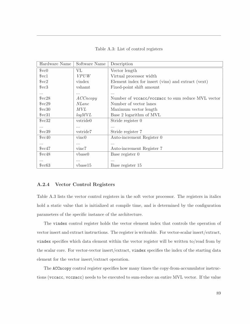
Table A.3: List of control registers
Hardware Name Software Name Description
$vc0 VL Vector length$vc1 VPUW Virtual processor width$vc2 vindex Element index for insert (vins) and extract (vext)$vc3 vshamt Fixed-point shift amount... ... ...$vc28 ACCncopy Number of vccacc/vcczacc to sum reduce MVL vector$vc29 NLane Number of vector lanes$vc30 MVL Maximum vector length$vc31 logMVL Base 2 logarithm of MVL
$vc32 vstride0 Stride register 0... ... ...$vc39 vstride7 Stride register 7
$vc40 vinc0 Auto-increment Register 0... ... ...$vc47 vinc7 Auto-increment Register 7
$vc48 vbase0 Base register 0... ... ...$vc63 vbase15 Base register 15
A.2.4 Vector Control Registers
Table A.3 lists the vector control registers in the soft vector processor. The registers in italics
hold a static value that is initialized at compile time, and is determined by the configuration
parameters of the specific instance of the architecture.
The vindex control register holds the vector element index that controls the operation of
vector insert and extract instructions. The register is writeable. For vector-scalar insert/extract,
vindex specifies which data element within the vector register will be written to/read from by
the scalar core. For vector-vector insert/extract, vindex specifies the index of the starting data
element for the vector insert/extract operation.
The ACCncopy control register specifies how many times the copy-from-accumulator instruc-
tions (vccacc, vcczacc) needs to be executed to sum-reduce an entire MVL vector. If the value
89

Appendix A. Soft Vector Processor ISA
is not one, multiple multiply-accumulate and copy-from-accumulator instructions will be needed
to reduce a MVL vector. Its usage will be discussed in more detail in Section A.2.5.
A.2.5 Multiply-Accumulators for Vector Sum Reduction
The architecture defines distributed MAC units for multiplying and sum reducing vectors. The
MAC units are distributed across the vector lanes, and the number of MAC units can vary
across implementations. The vmac instruction multiplies two inputs and accumulates the result
into accumulators within the MAC units. The vcczacc instruction sum reduces the MAC unit
accumulator contents, copies the final result to element zero of a vector register, and zeros the
accumulators. Together, the two instructions vmac and vcczacc perform a multiply and sum
reduce operation. Multiple vectors can be accumulated and sum reduced by executing vmac
multiple times. Since the MAC units sum multiplication products internally, they cannot be
used for purposes other than multiply-accumulate-sum reduce operations.
Depending on the number of vector lanes, the vcczacc instruction may not be able to sum
reduce all MAC unit accumulator contents. In such cases it will instead copy a partially sum-
reduced result vector to the destination register. Figure A.1 shows how the MAC units generate
a result vector and how the result vector is written to the vector register file. The MAC chain
length is specified by the MACL parameter. The vcczacc instruction sets VL to the length of
the partial result vector as a side effect, so the partial result vector can be again sum-reduced
using the vmac, vcczacc sequence. The ACCncopy control register specifies how many times
vcczacc needs to be executed (including the first) to reduce the entire MVL vector to a single
result in the destination register.
A.2.6 Vector Lane Local Memory
The soft vector architecture supports a vector lane local memory. The local memory is parti-
tioned into private sections for each VP if the LMemShare option is off. Turning the option
on allows the local memory block to be shared between all VPs in a vector lane. This mode is
90
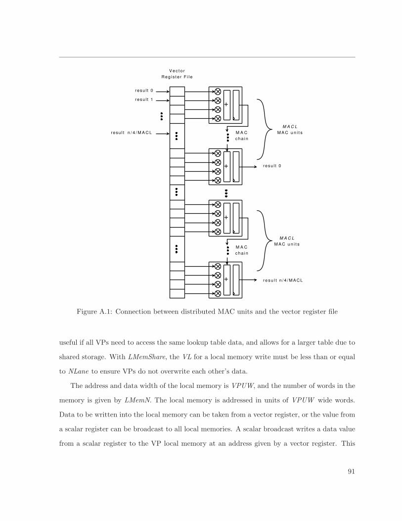
+
+
+
+
r esu l t 0
resu l t 0
r e s u l t n / 4 / M A C L
resu l t 1
V e c t o r
R e g i s t e r F i l e
M A C u n i t s
M A C L
M A C u n i t s
M A C L
r esu l t n / 4 / M A C L M A C
c h a i n
M A C
c h a i n
Figure A.1: Connection between distributed MAC units and the vector register file
useful if all VPs need to access the same lookup table data, and allows for a larger table due to
shared storage. With LMemShare, the VL for a local memory write must be less than or equal
to NLane to ensure VPs do not overwrite each other’s data.
The address and data width of the local memory is VPUW, and the number of words in the
memory is given by LMemN. The local memory is addressed in units of VPUW wide words.
Data to be written into the local memory can be taken from a vector register, or the value from
a scalar register can be broadcast to all local memories. A scalar broadcast writes a data value
from a scalar register to the VP local memory at an address given by a vector register. This
91
Appendix A. Soft Vector Processor ISA
facilitates filling the VP local memory with fixed lookup tables computed by the scalar unit.
A.3 Instruction Set
The following sections describe in detail the instruction set of the soft vector processor, and
different variations of the vector instructions.
A.3.1 Data Types
The data widths supported by the processor are 32-bit words, 16-bit halfwords, and 8-bit bytes,
and both signed and unsigned data types. However, not all operations are supported for 32-bit
words. Most notably, 32-bit multiply-accumulate is absent.
A.3.2 Addressing Modes
The instruction set supports three vector addressing modes:
1. Unit stride access
2. Constant stride access
3. Indexed offsets access
The vector lane local memory uses register addressing with no offset.
A.3.3 Flag Register Use
Almost all instructions can specify one of two vector mask registers in the opcode to use as
an execution mask. By default, vfmask0 is used as the vector mask. Writing a value of 1 into
the mask register will cause that VP to be disabled for operations that use the mask. Some
instructions, such as flag logical operations, are not masked.
A.3.4 Instructions
The instruction set includes the following categories of instructions:
92

1. Vector Integer Arithmetic Instructions
2. Vector Logical Instructions
3. Vector Fixed-Point Arithmetic Instructions
4. Vector Flag Processing Instructions
5. Vector Processing Intructions
6. Memory Instructions
A.4 Instruction Set Reference
The complete instruction set is listed in the following sections, separated by instruction type.
Table A.4 describes the possible qualifiers in the assembly mnemonic of each instruction.
Table A.4: Instruction qualifiers
Qualifier Meaning Notes
op.vv Vector-vector Vector arithmetic instructions may take one sourceoperand from a scalar register. A vector-vector operationtakes two vector source operands; a vector-scalar opera-tion takes its second operand from the scalar register file;a scalar-vector operation takes its first operand from thescalar register file. The .sv instruction type is providedto support non-commutative operations.
op.vs Vector-scalarop.sv Scalar-vector
op.b 1B ByteThe saturate instruction, and all vector memory instruc-tions need to specify the width of integer data.
op.h 2B Halfwordop.w 4B Word
op.1 Use vfmask1 as the mask By default, the vector mask is taken from vfmask0. Thisqualifier selects vfmask1 as the vector mask.
In the following tables, instructions in italics are not yet implemented.
A.4.1 Integer Instructions
93
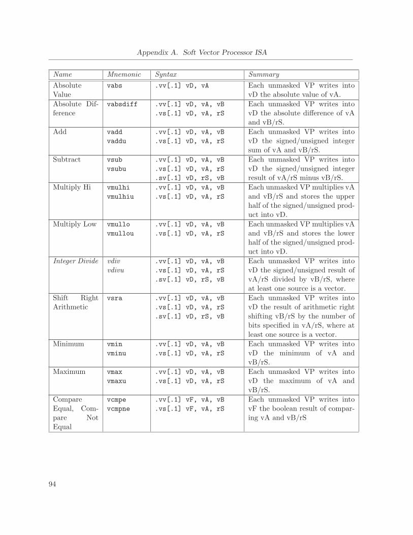
Appendix A. Soft Vector Processor ISA
Name Mnemonic Syntax Summary
AbsoluteValue
vabs .vv[.1] vD, vA Each unmasked VP writes intovD the absolute value of vA.
Absolute Dif-ference
vabsdiff .vv[.1] vD, vA, vB
.vs[.1] vD, vA, rS
Each unmasked VP writes intovD the absolute difference of vAand vB/rS.
Add vadd
vaddu
.vv[.1] vD, vA, vB
.vs[.1] vD, vA, rS
Each unmasked VP writes intovD the signed/unsigned integersum of vA and vB/rS.
Subtract vsub
vsubu
.vv[.1] vD, vA, vB
.vs[.1] vD, vA, rS
.sv[.1] vD, rS, vB
Each unmasked VP writes intovD the signed/unsigned integerresult of vA/rS minus vB/rS.
Multiply Hi vmulhi
vmulhiu
.vv[.1] vD, vA, vB
.vs[.1] vD, vA, rS
Each unmasked VP multiplies vAand vB/rS and stores the upperhalf of the signed/unsigned prod-uct into vD.
Multiply Low vmullo
vmullou
.vv[.1] vD, vA, vB
.vs[.1] vD, vA, rS
Each unmasked VP multiplies vAand vB/rS and stores the lowerhalf of the signed/unsigned prod-uct into vD.
Integer Divide vdivvdivu
.vv[.1] vD, vA, vB
.vs[.1] vD, vA, rS
.sv[.1] vD, rS, vB
Each unmasked VP writes intovD the signed/unsigned result ofvA/rS divided by vB/rS, whereat least one source is a vector.
Shift RightArithmetic
vsra .vv[.1] vD, vA, vB
.vs[.1] vD, vA, rS
.sv[.1] vD, rS, vB
Each unmasked VP writes intovD the result of arithmetic rightshifting vB/rS by the number ofbits specified in vA/rS, where atleast one source is a vector.
Minimum vmin
vminu
.vv[.1] vD, vA, vB
.vs[.1] vD, vA, rS
Each unmasked VP writes intovD the minimum of vA andvB/rS.
Maximum vmax
vmaxu
.vv[.1] vD, vA, vB
.vs[.1] vD, vA, rS
Each unmasked VP writes intovD the maximum of vA andvB/rS.
CompareEqual, Com-pare NotEqual
vcmpe
vcmpne
.vv[.1] vF, vA, vB
.vs[.1] vF, vA, rS
Each unmasked VP writes intovF the boolean result of compar-ing vA and vB/rS
94

Name Mnemonic Syntax Summary
Compare LessThan
vcmplt
vcmpltu
.vv[.1] vF, vA, vB
.vs[.1] vF, vA, rS
.sv[.1] vF, rS, vB
Each unmasked VP writes intovF the boolean result of whethervA/rS is less than vB/rS, whereat least one source is a vector.
CompareLess Than orEqual
vcmple
vcmpleu
.vv[.1] vF, vA, vB
.vs[.1] vF, vA, rS
.sv[.1] vF, rS, vB
Each unmasked VP writes intovF the boolean result of whethervA/rS is less than or equal tovB/rS, where at least one sourceis a vector.
Multiply Ac-cumulate
vmac
vmacu
.vv[.1] vA, vB
.vs[.1] vD, vA, rS
Each unmasked VP calculates theproduct of vA and vB/rS. Theproducts of vector elements aresummed, and the summation re-sults are added to the distributedaccumulators.
CompressCopy fromAccumulator
vccacc vD The contents of the distributedaccumulators are reduced, andthe result written into vD. Onlythe bottom VPUW bits of the re-sult are written. If the numberof accumulators is greater thanMACL, multiple partial resultswill be generated by the accu-mulate chain, and they are com-pressed such that the partial re-sults form a contiguous vector invD. If the number of accumu-lators is less than or equal toMACL, a single result is writteninto element zero of vD. This in-struction is not masked and theelements of vD beyond the par-tial result vector length are notmodified. Additionally, VL is setto the number of elements in thepartial result vector as a side ef-fect.
CompressCopy andZero Accumu-lator
vcczacc vD The operation is identical tovccacc, except the distributedaccumulators are zeroed as a sideeffect.
95
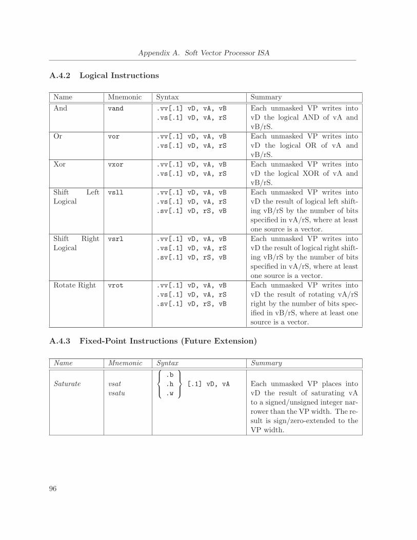
Appendix A. Soft Vector Processor ISA
A.4.2 Logical Instructions
Name Mnemonic Syntax Summary
And vand .vv[.1] vD, vA, vB
.vs[.1] vD, vA, rS
Each unmasked VP writes intovD the logical AND of vA andvB/rS.
Or vor .vv[.1] vD, vA, vB
.vs[.1] vD, vA, rS
Each unmasked VP writes intovD the logical OR of vA andvB/rS.
Xor vxor .vv[.1] vD, vA, vB
.vs[.1] vD, vA, rS
Each unmasked VP writes intovD the logical XOR of vA andvB/rS.
Shift LeftLogical
vsll .vv[.1] vD, vA, vB
.vs[.1] vD, vA, rS
.sv[.1] vD, rS, vB
Each unmasked VP writes intovD the result of logical left shift-ing vB/rS by the number of bitsspecified in vA/rS, where at leastone source is a vector.
Shift RightLogical
vsrl .vv[.1] vD, vA, vB
.vs[.1] vD, vA, rS
.sv[.1] vD, rS, vB
Each unmasked VP writes intovD the result of logical right shift-ing vB/rS by the number of bitsspecified in vA/rS, where at leastone source is a vector.
Rotate Right vrot .vv[.1] vD, vA, vB
.vs[.1] vD, vA, rS
.sv[.1] vD, rS, vB
Each unmasked VP writes intovD the result of rotating vA/rSright by the number of bits spec-ified in vB/rS, where at least onesource is a vector.
A.4.3 Fixed-Point Instructions (Future Extension)
Name Mnemonic Syntax Summary
Saturate vsatvsatu
.b
.h
.w
[.1] vD, vA Each unmasked VP places intovD the result of saturating vAto a signed/unsigned integer nar-rower than the VP width. The re-sult is sign/zero-extended to theVP width.
96

Name Mnemonic Syntax Summary
SaturateSigned toUnsigned
vsatsu
.b
.h
.w
[.1] vD, vA Each unmasked VP places intovD the result of saturating vAfrom a signed VP width value toan unsigned value that is as wideor narrower than the VP width.The result is zero-extended to theVP width.
SaturatingAdd
vsaddvsaddu
.vv[.1] vD, vA, vB
.vs[.1] vD, vA, rS
Each unmasked VP writes intovD the signed/unsigned integersum of vA and vB/rS. The sumsaturates to the VP width insteadof overflowing.
SaturatingSubtract
vssubvssubu
.vv[.1] vD, vA, vB
.vs[.1] vD, vA, rS
.sv[.1] vD, rS, vB
Each unmasked VP writes intovD the signed/unsigned integersubtraction of vA/rS and vB/rS,where at least one source is a vec-tor. The difference saturates tothe VP width instead of overflow-ing.
Shift Rightand Round
vsrrvsrru
[.1] vD, vA Each unmasked VP writes intovD the right arithmetic/logicalshift of vD. The result is roundedas per the fixed-point roundingmode. The shift amount is takenfrom vcvshamt.
SaturatingLeft Shift
vslsvslsu
[.1] vD, vA Each unmasked VP writes intovD the signed/unsigned saturat-ing left shift of vD. The shiftamount is taken from vcvshamt.
Multiply High vxmulhivxmulhiu
.vv[.1] vD, vA, vB
.vs[.1] vD, vA, rS
Each unmasked VP computes thesigned/unsigned integer productof vA and vB/rS, and stores theupper half of the product intovD after arithmetic right shiftand fixed-point round. The shiftamount is taken from vcvshamt
97
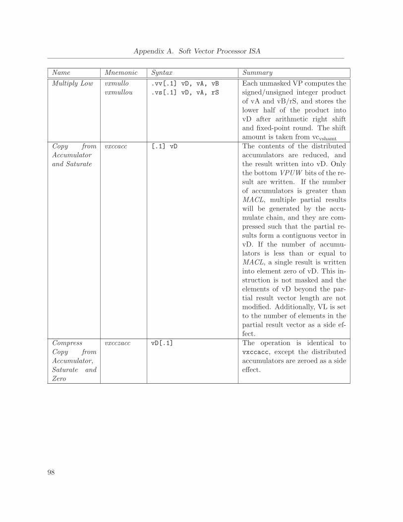
Appendix A. Soft Vector Processor ISA
Name Mnemonic Syntax Summary
Multiply Low vxmullovxmullou
.vv[.1] vD, vA, vB
.vs[.1] vD, vA, rS
Each unmasked VP computes thesigned/unsigned integer productof vA and vB/rS, and stores thelower half of the product intovD after arithmetic right shiftand fixed-point round. The shiftamount is taken from vcvshamt
Copy fromAccumulatorand Saturate
vxccacc [.1] vD The contents of the distributedaccumulators are reduced, andthe result written into vD. Onlythe bottom VPUW bits of the re-sult are written. If the numberof accumulators is greater thanMACL, multiple partial resultswill be generated by the accu-mulate chain, and they are com-pressed such that the partial re-sults form a contiguous vector invD. If the number of accumu-lators is less than or equal toMACL, a single result is writteninto element zero of vD. This in-struction is not masked and theelements of vD beyond the par-tial result vector length are notmodified. Additionally, VL is setto the number of elements in thepartial result vector as a side ef-fect.
CompressCopy fromAccumulator,Saturate andZero
vxcczacc vD[.1] The operation is identical tovxccacc, except the distributedaccumulators are zeroed as a sideeffect.
98
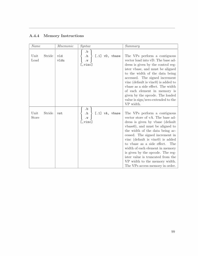
A.4.4 Memory Instructions
Name Mnemonic Syntax Summary
Unit StrideLoad
vld
vldu
.b
.h
.w
[.1] vD, vbase
[,vinc]
The VPs perform a contiguousvector load into vD. The base ad-dress is given by the control reg-ister vbase, and must be alignedto the width of the data beingaccessed. The signed incrementvinc (default is vinc0) is added tovbase as a side effect. The widthof each element in memory isgiven by the opcode. The loadedvalue is sign/zero-extended to theVP width.
Unit StrideStore
vst
.b
.h
.w
[.1] vA, vbase
[,vinc]
The VPs perform a contiguousvector store of vA. The base ad-dress is given by vbase (defaultvbase0), and must be aligned tothe width of the data being ac-cessed. The signed increment invinc (default is vinc0) is addedto vbase as a side effect. Thewidth of each element in memoryis given by the opcode. The reg-ister value is truncated from theVP width to the memory width.The VPs access memory in order.
99
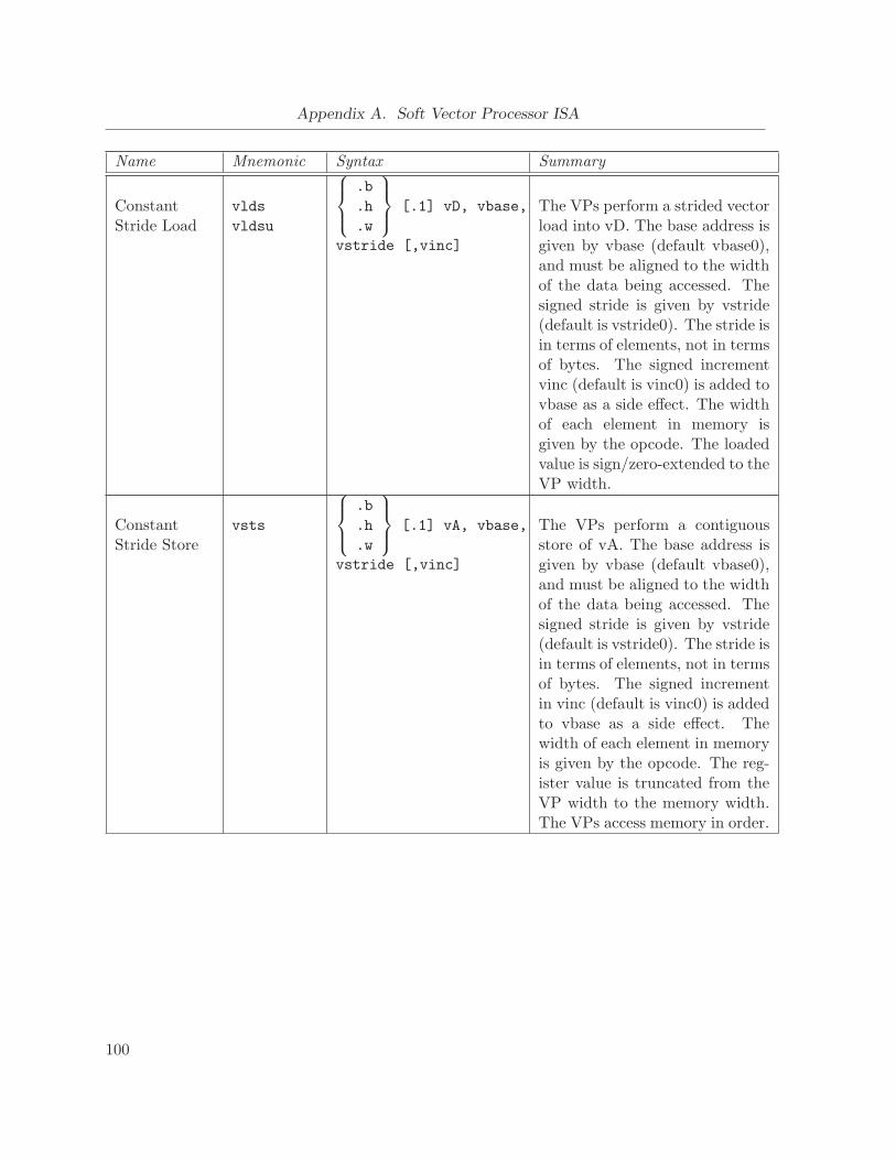
Appendix A. Soft Vector Processor ISA
Name Mnemonic Syntax Summary
ConstantStride Load
vlds
vldsu
.b
.h
.w
[.1] vD, vbase,
vstride [,vinc]
The VPs perform a strided vectorload into vD. The base address isgiven by vbase (default vbase0),and must be aligned to the widthof the data being accessed. Thesigned stride is given by vstride(default is vstride0). The stride isin terms of elements, not in termsof bytes. The signed incrementvinc (default is vinc0) is added tovbase as a side effect. The widthof each element in memory isgiven by the opcode. The loadedvalue is sign/zero-extended to theVP width.
ConstantStride Store
vsts
.b
.h
.w
[.1] vA, vbase,
vstride [,vinc]
The VPs perform a contiguousstore of vA. The base address isgiven by vbase (default vbase0),and must be aligned to the widthof the data being accessed. Thesigned stride is given by vstride(default is vstride0). The stride isin terms of elements, not in termsof bytes. The signed incrementin vinc (default is vinc0) is addedto vbase as a side effect. Thewidth of each element in memoryis given by the opcode. The reg-ister value is truncated from theVP width to the memory width.The VPs access memory in order.
100
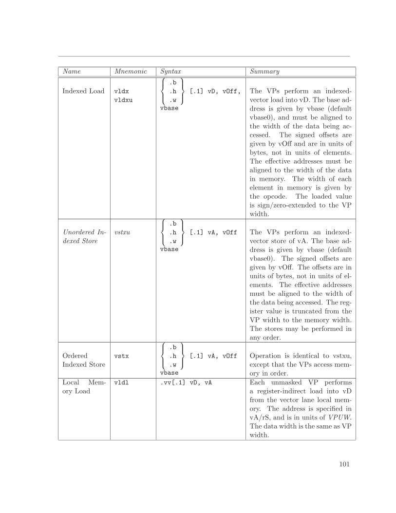
Name Mnemonic Syntax Summary
Indexed Load vldx
vldxu
.b
.h
.w
[.1] vD, vOff,
vbase
The VPs perform an indexed-vector load into vD. The base ad-dress is given by vbase (defaultvbase0), and must be aligned tothe width of the data being ac-cessed. The signed offsets aregiven by vOff and are in units ofbytes, not in units of elements.The effective addresses must bealigned to the width of the datain memory. The width of eachelement in memory is given bythe opcode. The loaded valueis sign/zero-extended to the VPwidth.
Unordered In-dexed Store
vstxu
.b
.h
.w
[.1] vA, vOff
vbase
The VPs perform an indexed-vector store of vA. The base ad-dress is given by vbase (defaultvbase0). The signed offsets aregiven by vOff. The offsets are inunits of bytes, not in units of el-ements. The effective addressesmust be aligned to the width ofthe data being accessed. The reg-ister value is truncated from theVP width to the memory width.The stores may be performed inany order.
OrderedIndexed Store
vstx
.b
.h
.w
[.1] vA, vOff
vbase
Operation is identical to vstxu,except that the VPs access mem-ory in order.
Local Mem-ory Load
vldl .vv[.1] vD, vA Each unmasked VP performsa register-indirect load into vDfrom the vector lane local mem-ory. The address is specified invA/rS, and is in units of VPUW.The data width is the same as VPwidth.
101
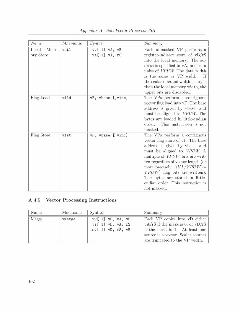
Appendix A. Soft Vector Processor ISA
Name Mnemonic Syntax Summary
Local Mem-ory Store
vstl .vv[.1] vA, vB
.vs[.1] vA, rS
Each unmasked VP performs aregister-indirect store of vB/rSinto the local memory. The ad-dress is specified in vA, and is inunits of VPUW. The data widthis the same as VP width. Ifthe scalar operand width is largerthan the local memory width, theupper bits are discarded.
Flag Load vfld vF, vbase [,vinc] The VPs perform a contiguousvector flag load into vF. The baseaddress is given by vbase, andmust be aligned to VPUW. Thebytes are loaded in little-endianorder. This instruction is notmasked.
Flag Store vfst vF, vbase [,vinc] The VPs perform a contiguousvector flag store of vF. The baseaddress is given by vbase, andmust be aligned to VPUW. Amultiple of VPUW bits are writ-ten regardless of vector length (ormore precisely, ⌈(V L/V PUW ) ∗V PUW ⌉ flag bits are written).The bytes are stored in little-endian order. This instruction isnot masked.
A.4.5 Vector Processing Instructions
Name Mnemonic Syntax Summary
Merge vmerge .vv[.1] vD, vA, vB
.vs[.1] vD, vA, rS
.sv[.1] vD, rS, vB
Each VP copies into vD eithervA/rS if the mask is 0, or vB/rSif the mask is 1. At least onesource is a vector. Scalar sourcesare truncated to the VP width.
102

Vector Insert vins .vv vD, vA The leading portion of vA is in-serted into vD. vD must be differ-ent from vA. Leading and trail-ing entries of vD are not touched.The lower vclogmvl bits of vectorcontrol register vcvindex specifiesthe starting position in vD. Thevector length specifies the num-ber of elements to transfer. Thisinstruction is not masked.
Vector Ex-tract
vext .vv vD, vA A portion of vA is extracted tothe front of vD. vD must be dif-ferent from vA. Trailing entries ofvD are not touched. The lowervclogmvl bits of vector control reg-ister vcvindex specifies the startingposition in vD. The vector lengthspecifies the number of elementsto transfer. This instruction isnot masked.
Scalar Insert vins .vs vD, rS The contents of rS are writteninto vD at position vcvindex. Thelower vclogmvl bits of vcvindex areused. This instruction is notmasked and does not use vectorlength.
Scalar Ex-tract
vext
vextu
.vs rS, vA Element vcvindex of vA is writ-ten into rS. The lower vclogmvl
bits of vcindex are used to deter-mine the element in vA to be ex-tracted. The value is sign/zero-extended. This instruction is notmasked and does not use vectorlength.
Compress vcomp [.1] vD, vA All unmasked elements of vA areconcatenated to form a vectorwhose length is the populationcount of the ask (subject to vec-tor length). The result is placedat the front of vD, leaving trailingelements untouched. vD must bedifferent from vA.
103
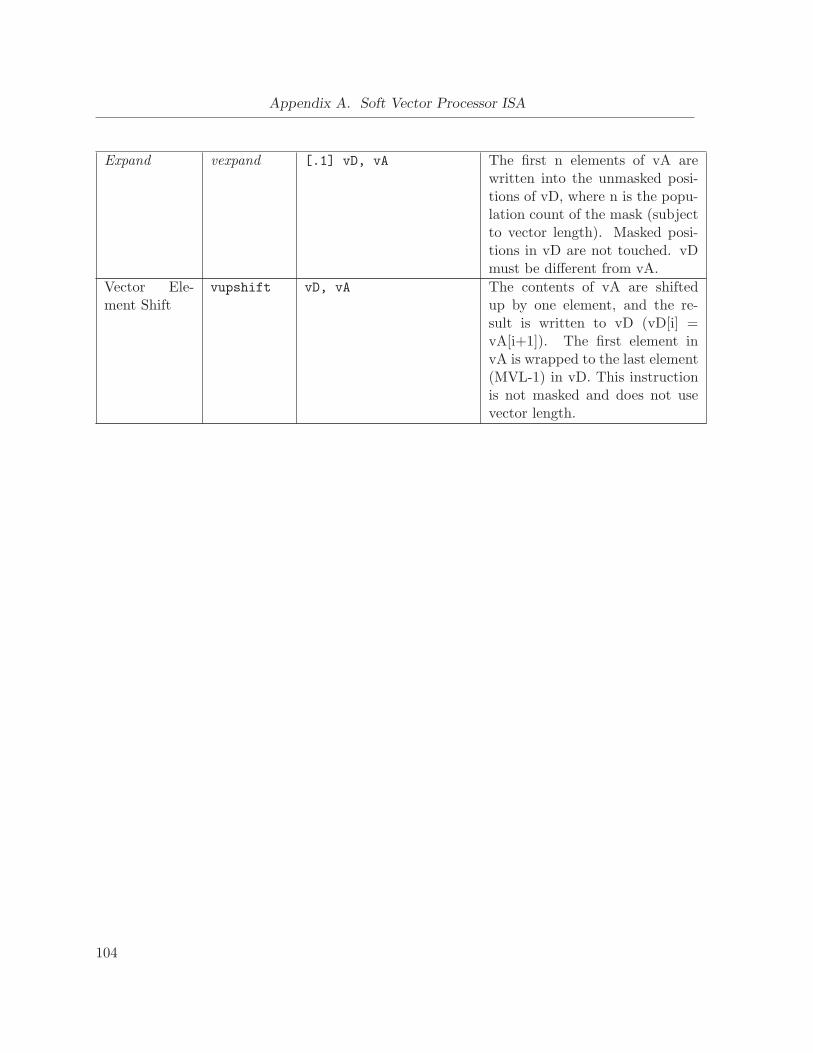
Appendix A. Soft Vector Processor ISA
Expand vexpand [.1] vD, vA The first n elements of vA arewritten into the unmasked posi-tions of vD, where n is the popu-lation count of the mask (subjectto vector length). Masked posi-tions in vD are not touched. vDmust be different from vA.
Vector Ele-ment Shift
vupshift vD, vA The contents of vA are shiftedup by one element, and the re-sult is written to vD (vD[i] =vA[i+1]). The first element invA is wrapped to the last element(MVL-1) in vD. This instructionis not masked and does not usevector length.
104

A.4.6 Vector Flag Processing Instructions
Name Mnemonic Syntax Summary
Scalar FlagInsert
vfins .vs vF, rS The boolean value of rS is writ-ten into vF at position vcvindex.The lower vclogmvl bits of vcvindex
are used. This instruction is notmasked and does not use vectorlength.
And vfand .vv vFD, vFA, vFB
.vs vFD, vFA, rS
Each VP writes into vFD the log-ical AND of vFA and vFB/rS.This instruction is not masked,but is subject to vector length.
Or vfor .vv vFD, vFA, vFB
.vs vFD, vFA, rS
Each VP writes into vFD the log-ical OR of vFA and vFB/rS. Thisinstruction is not masked, but issubject to vector length.
Xor vfxor .vv vFD, vFA, vFB
.vs vFD, vFA, rS
Each VP writes into vFD the log-ical XOR of vFA and vFB/rS.This instruction is not masked,but is subject to vector length.
Nor vfnor .vv vFD, vFA, vFB
.vs vFD, vFA, rS
Each VP writes into vFD the log-ical NOR of vFA and vFB/rS.This instruction is not masked,but is subject to vector length.
Clear vfclr vFD Each VP writes zero into vFD.This instruction is not masked,but is subject to vector length.
Set vfset vFD Each VP writes one into vFD.This instruction is not masked,but is subject to vector length.
PopulationCount
vfpop rS, vF The population count of vF isplaced in rS. This instruction isnot masked.
Find FirstOne
vfff1 rS, vF The location of the first set bit ofvF is placed in rS. This instruc-tion is not masked. If there isno set bit in vF, then the vectorlength is placed in rS.
105

Appendix A. Soft Vector Processor ISA
Find LastOne
vffl1 rS, vF The location of the last set bit ofvF is placed in rS. The instruc-tion is not masked. If there isno set bit in vF, then the vectorlength is placed in rS.
Set BeforeFirst One
vfsetbf vFD, vFA Register vFD is filled with onesup to and not including the firstset bit in vFA. Remaining posi-tions in vF are cleared. If vFAcontains no set bits, vFD is set toall ones. This instruction is notmasked.
Set IncludingFirst One
vfsetif vFD, vFA Register vFD is filled with onesup to and including the first setbit in vFA. Remaining positionsin vF are cleared. If vFA containsno set bits, vFD is set to all ones.This instruction is not masked.
Set Only FirstOne
vfsetof vFD, vFA Register vFD is filled with zerosexcept for the position of the firstset bit in vFA. If vFA contains noset bits, vFD is set to all zeros.This instruction is not masked.
A.4.7 Miscellaneous Instructions
Name Mnemonic Syntax Summary
Move Scalarto Control
vmstc vc, rS Register rS is copied to vc. Writ-ing vcvpw changes vcmvl, vclogmvl
as a side effect.
Move Controlto Scalar
vmcts rS, vc Register vc is copied to rS.
106
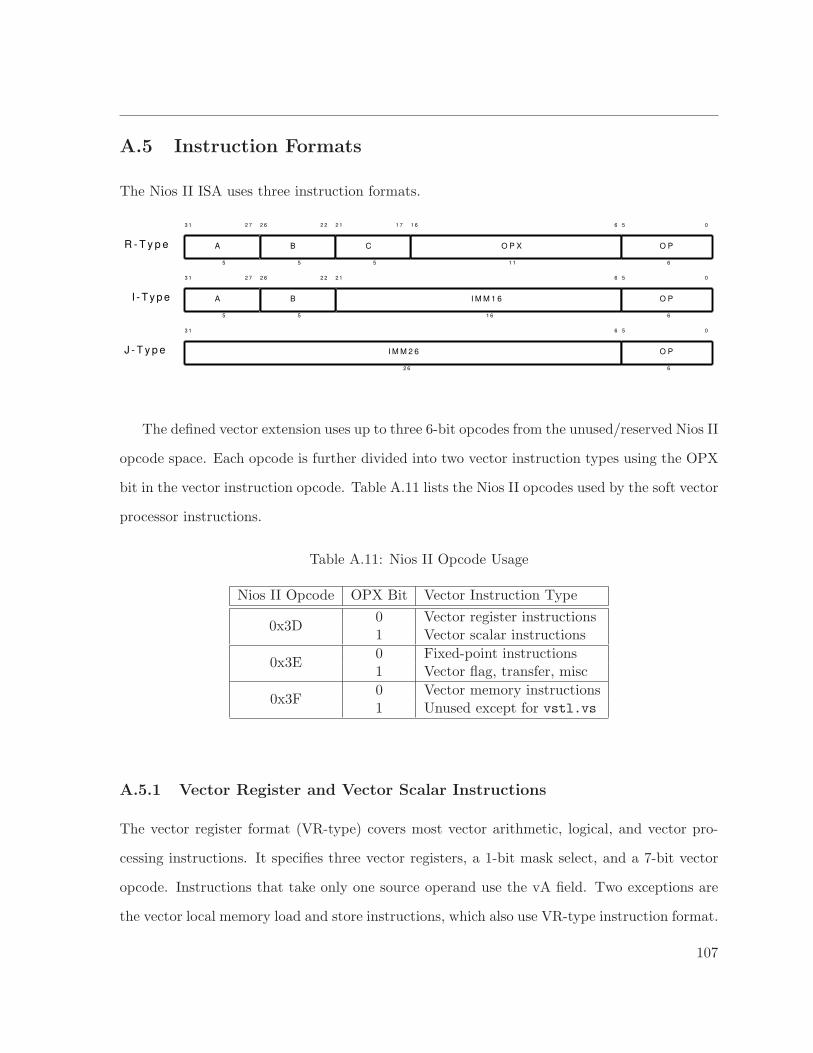
A.5 Instruction Formats
The Nios II ISA uses three instruction formats.
R - T y p e A O P X O P
3 1 2 7 2 6 2 2 2 1 1 7 1 6 6 5 0
5 1 1 6
B
5
C
5
A I M M 1 6 O P
3 1 2 7 2 6 2 2 2 1 6 5 0
5 1 6 6
B
5
I - T y p e
I M M 2 6 O P
3 1 6 5 0
2 6 6
J - T y p e
The defined vector extension uses up to three 6-bit opcodes from the unused/reserved Nios II
opcode space. Each opcode is further divided into two vector instruction types using the OPX
bit in the vector instruction opcode. Table A.11 lists the Nios II opcodes used by the soft vector
processor instructions.
Table A.11: Nios II Opcode Usage
Nios II Opcode OPX Bit Vector Instruction Type
0x3D0 Vector register instructions1 Vector scalar instructions
0x3E0 Fixed-point instructions1 Vector flag, transfer, misc
0x3F0 Vector memory instructions1 Unused except for vstl.vs
A.5.1 Vector Register and Vector Scalar Instructions
The vector register format (VR-type) covers most vector arithmetic, logical, and vector pro-
cessing instructions. It specifies three vector registers, a 1-bit mask select, and a 7-bit vector
opcode. Instructions that take only one source operand use the vA field. Two exceptions are
the vector local memory load and store instructions, which also use VR-type instruction format.
107
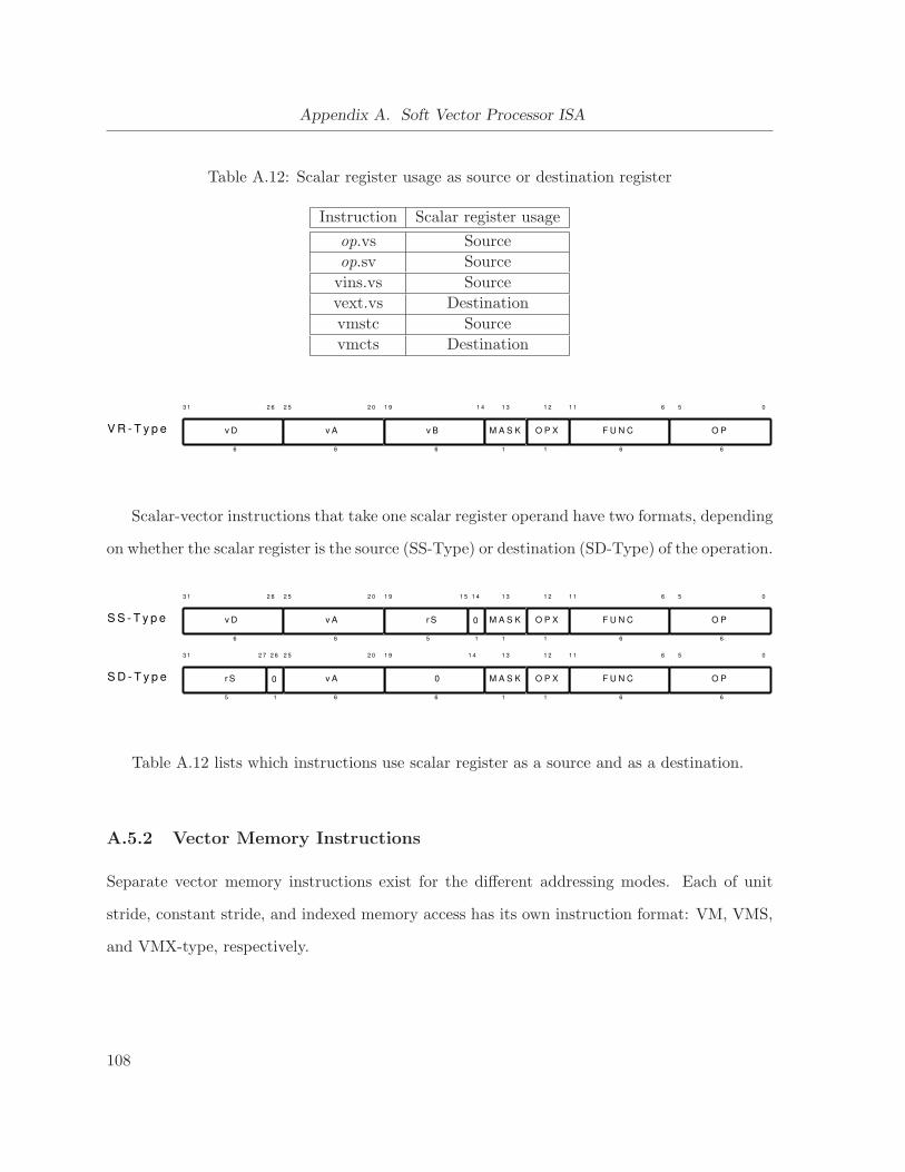
Appendix A. Soft Vector Processor ISA
Table A.12: Scalar register usage as source or destination register
Instruction Scalar register usage
op.vs Source
op.sv Source
vins.vs Source
vext.vs Destination
vmstc Source
vmcts Destination
V R - T y p e v D v A v B F U N C O PM A S K O P X
3 1 2 6 2 5 2 0 1 9 1 4 1 3 1 2 1 1 6 5 0
6 6 6 1 1 6 6
Scalar-vector instructions that take one scalar register operand have two formats, depending
on whether the scalar register is the source (SS-Type) or destination (SD-Type) of the operation.
S S - T y p e v D v A r S F U N C O PM A S K O P X
3 1 2 6 2 5 2 0 1 9 1 4 1 3 1 2 1 1 6 5 0
6 6 5 1 1 6 6
0
1 5
1
0v Ar S F U N C O PM A S K O P X
1 9 1 42 5 2 03 1 2 6 1 3 1 2 1 1 6 5 0
665 1 1 6 6
0
2 7
1
S D - T y p e
Table A.12 lists which instructions use scalar register as a source and as a destination.
A.5.2 Vector Memory Instructions
Separate vector memory instructions exist for the different addressing modes. Each of unit
stride, constant stride, and indexed memory access has its own instruction format: VM, VMS,
and VMX-type, respectively.
108
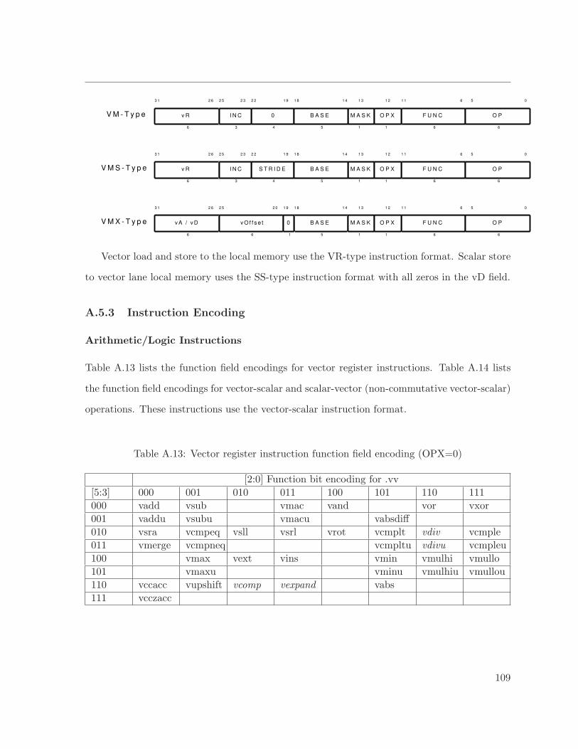
V M - T y p e v R F U N C O PM A S K O P X
3 1 2 6 2 5 1 9 1 8 1 4 1 3 1 2 1 1 6 5 0
V M X - T y p e v A / v D v O f f s e t B A S E F U N C O PM A S K O P X
3 1 2 6 2 5 2 0 1 9 1 4 1 3 1 2 1 1 6 5 0
V M S - T y p e
0
1 8
B A S E
2 22 3
I N C
v R
0
F U N C O PM A S K O P X
3 1 2 6 2 5 1 9 1 8 1 4 1 3 1 2 1 1 6 5 0
B A S E
2 22 3
I N C
6 3 4 5 1 1 6 6
6 3 4 5 1 1 6 6
6 6 1 5 1 1 6 6
S T R I D E
Vector load and store to the local memory use the VR-type instruction format. Scalar store
to vector lane local memory uses the SS-type instruction format with all zeros in the vD field.
A.5.3 Instruction Encoding
Arithmetic/Logic Instructions
Table A.13 lists the function field encodings for vector register instructions. Table A.14 lists
the function field encodings for vector-scalar and scalar-vector (non-commutative vector-scalar)
operations. These instructions use the vector-scalar instruction format.
Table A.13: Vector register instruction function field encoding (OPX=0)
[2:0] Function bit encoding for .vv
[5:3] 000 001 010 011 100 101 110 111
000 vadd vsub vmac vand vor vxor
001 vaddu vsubu vmacu vabsdiff
010 vsra vcmpeq vsll vsrl vrot vcmplt vdiv vcmple
011 vmerge vcmpneq vcmpltu vdivu vcmpleu
100 vmax vext vins vmin vmulhi vmullo
101 vmaxu vminu vmulhiu vmullou
110 vccacc vupshift vcomp vexpand vabs
111 vcczacc
109
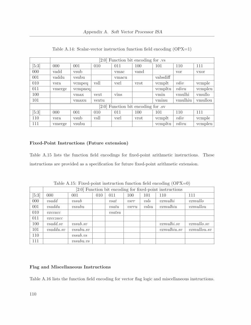
Appendix A. Soft Vector Processor ISA
Table A.14: Scalar-vector instruction function field encoding (OPX=1)
[2:0] Function bit encoding for .vs
[5:3] 000 001 010 011 100 101 110 111
000 vadd vsub vmac vand vor vxor
001 vaddu vsubu vmacu vabsdiff
010 vsra vcmpeq vsll vsrl vrot vcmplt vdiv vcmple
011 vmerge vcmpneq vcmpltu vdivu vcmpleu
100 vmax vext vins vmin vmulhi vmullo
101 vmaxu vextu vminu vmulhiu vmullou
[2:0] Function bit encoding for .sv
[5:3] 000 001 010 011 100 101 110 111
110 vsra vsub vsll vsrl vrot vcmplt vdiv vcmple
111 vmerge vsubu vcmpltu vdivu vcmpleu
Fixed-Point Instructions (Future extension)
Table A.15 lists the function field encodings for fixed-point arithmetic instructions. These
instructions are provided as a specification for future fixed-point arithmetic extension.
Table A.15: Fixed-point instruction function field encoding (OPX=0)
[2:0] Function bit encoding for fixed-point instructions
[5:3] 000 001 010 011 100 101 110 111
000 vsadd vssub vsat vsrr vsls vxmulhi vxmullo
001 vsaddu vssubu vsatu vsrru vslsu vxmulhiu vxmullou
010 vxccacc vsatsu
011 vxcczacc
100 vsadd.sv vssub.sv vxmulhi.sv vxmullo.sv
101 vsaddu.sv vssubu.sv vxmulhiu.sv vxmullou.sv
110 vssub.vs
111 vssubu.vs
Flag and Miscellaneous Instructions
Table A.16 lists the function field encoding for vector flag logic and miscellaneous instructions.
110

Table A.16: Flag and miscellaneous instruction function field encoding (OPX=1)
[2:0] Function bit encoding for flag/misc instructions
[5:3] 000 001 010 011 100 101 110 111
000 vfclr vfset vfand vfnor vfor vfxor
001 vfff1 vffl1
010 vfsetof vfsetbf vfsetif
011 vfins.vs vfand.vs vfnor.vs vfor.vs vfxor.vs
100
101 vmstc vmcts
110
111
Memory Instructions
Table A.17 lists the function field encoding for vector memory instructions. The vector-scalar
instruction vstl.vs is the only instruction that has opcode of 0x3F and OPX bit of 1.
Table A.17: Memory instruction function field encoding
[2:0] Function bit encoding for memory instructions (OPX=0)
[5:3] 000 001 010 011 100 101 110 111
000 vld.b vst.b vlds.b vsts.b vldx.b vstxu.b vstx.b
001 vldu.b vldsu.b vldxu.b
010 vld.h vst.h vlds.h vsts.h vldx.h vstxu.h vstx.h
011 vldu.h vldsu.h vldxu.h
100 vld.w vst.w vlds.w vsts.w vldx.w vstxu.w vstx.w
101
110 vldl vstl vfld vfst
111
[2:0] Function bit encoding for memory instructions (OPX=1)
[5:3] 000 001 010 011 100 101 110 111
110 vstl.vs
111
Related Documents