1 V54C3128(16/80/40)4VB*I 128Mbit SDRAM, INDUSTRIAL TEMPERATURE 3.3 VOLT, TSOP II / FBGA 8M X 16, 16M X 8, 32M X 4 V54C3128(16/80/40)4VB*I Rev. 1.5 June 2008 6 7PC 7 System Frequency (f CK ) 166 MHz 143 MHz 143 MHz Clock Cycle Time (t CK3 ) 6 ns 7 ns 7 ns Clock Access Time (t AC3 ) CAS Latency = 3 5.4 ns 5.4 ns 5.4 ns Clock Access Time (t AC2 ) CAS Latency = 2 5.4 ns 5.4 ns 6 ns Features ■ 4 banks x 2Mbit x 16 organization ■ 4 banks x 4Mbit x 8 organization ■ 4 banks x 8Mbit x 4 organization ■ High speed data transfer rates up to 166 MHz ■ Full Synchronous Dynamic RAM, with all signals referenced to clock rising edge ■ Single Pulsed RAS Interface ■ Data Mask for Read/Write Control ■ Four Banks controlled by BA0 & BA1 ■ Programmable CAS Latency: 2, 3 ■ Programmable Wrap Sequence: Sequential or Interleave ■ Programmable Burst Length: 1, 2, 4, 8, and full page for Sequential Type 1, 2, 4, 8 for Interleave Type ■ Multiple Burst Read with Single Write Operation ■ Automatic and Controlled Precharge Command ■ Random Column Address every CLK (1-N Rule) ■ Power Down Mode ■ Auto Refresh and Self Refresh ■ Refresh Interval: 4096 cycles/64 ms ■ Available in 54-ball FBGA, 60-ball FBGA and 54-Pin TSOPII ■ LVTTL Interface ■ Single (+3.0 V ~3.3V)±0.3 V Power Supply ■ Industrial Temperature (TA): -40C to +85C Description The V54C3128(16/80/40)4VB*I is a four bank Synchronous DRAM organized as 4 banks x 2Mbit x 16, 4 banks x 4Mbit x 8, or 4 banks x 8Mbit x 4. The V54C3128(16/80/40)4VB*I achieves high speed data transfer rates up to 166 MHz by employ- ing a chip architecture that prefetches multiple bits and then synchronizes the output data to a system clock. All of the control, address, data input and output circuits are synchronized with the positive edge of an externally supplied clock. Operating the four memory banks in an inter- leaved fashion allows random access operation to occur at higher rate than is possible with standard DRAMs. A sequential and gapless data rate of up to 166 MHz is possible depending on burst length, CAS latency and speed grade of the device. Device Usage Chart Operating Temperature Range Package Outline Access Time (ns) Power Temperature Mark C/S/T 6 7PC 7 Std. L -40°C to +85°C • • • • • • I

Welcome message from author
This document is posted to help you gain knowledge. Please leave a comment to let me know what you think about it! Share it to your friends and learn new things together.
Transcript
V54C3128(16/80/40)4VB*I128Mbit SDRAM, INDUSTRIAL TEMPERATURE3.3 VOLT, TSOP II / FBGA8M X 16, 16M X 8, 32M X 4
6 7PC 7
System Frequency (fCK) 166 MHz 143 MHz 143 MHz
Clock Cycle Time (tCK3) 6 ns 7 ns 7 ns
Clock Access Time (tAC3) CAS Latency = 3 5.4 ns 5.4 ns 5.4 ns
Clock Access Time (tAC2) CAS Latency = 2 5.4 ns 5.4 ns 6 ns
Features■ 4 banks x 2Mbit x 16 organization■ 4 banks x 4Mbit x 8 organization■ 4 banks x 8Mbit x 4 organization■ High speed data transfer rates up to 166 MHz■ Full Synchronous Dynamic RAM, with all signals
referenced to clock rising edge■ Single Pulsed RAS Interface■ Data Mask for Read/Write Control■ Four Banks controlled by BA0 & BA1■ Programmable CAS Latency: 2, 3■ Programmable Wrap Sequence: Sequential or
Interleave■ Programmable Burst Length:
1, 2, 4, 8, and full page for Sequential Type1, 2, 4, 8 for Interleave Type
■ Multiple Burst Read with Single Write Operation■ Automatic and Controlled Precharge Command■ Random Column Address every CLK (1-N Rule)■ Power Down Mode■ Auto Refresh and Self Refresh■ Refresh Interval: 4096 cycles/64 ms■ Available in 54-ball FBGA, 60-ball FBGA and
54-Pin TSOPII■ LVTTL Interface■ Single (+3.0 V ~3.3V)±0.3 V Power Supply■ Industrial Temperature (TA): -40C to +85C
DescriptionThe V54C3128(16/80/40)4VB*I is a four bank
Synchronous DRAM organized as 4 banks x 2Mbitx 16, 4 banks x 4Mbit x 8, or 4 banks x 8Mbit x 4.The V54C3128(16/80/40)4VB*I achieves highspeed data transfer rates up to 166 MHz by employ-ing a chip architecture that prefetches multiple bitsand then synchronizes the output data to a systemclock.
All of the control, address, data input and outputcircuits are synchronized with the positive edge ofan externally supplied clock.
Operating the four memory banks in an inter-leaved fashion allows random access operation tooccur at higher rate than is possible with standardDRAMs. A sequential and gapless data rate of up to166 MHz is possible depending on burst length,CAS latency and speed grade of the device.
1V54C3128(16/80/40)4VB*I Rev. 1.5 June 2008
Device Usage Chart
OperatingTemperature
Range
Package Outline Access Time (ns) PowerTemperature
MarkC/S/T 6 7PC 7 Std. L
-40°C to +85°C • • • • • • I
2V54C3128(16/80/40)4VB*I Rev.1.5 June 2008
ProMOS TECHNOLOGIES V54C3128(16/80/40)4VB*I
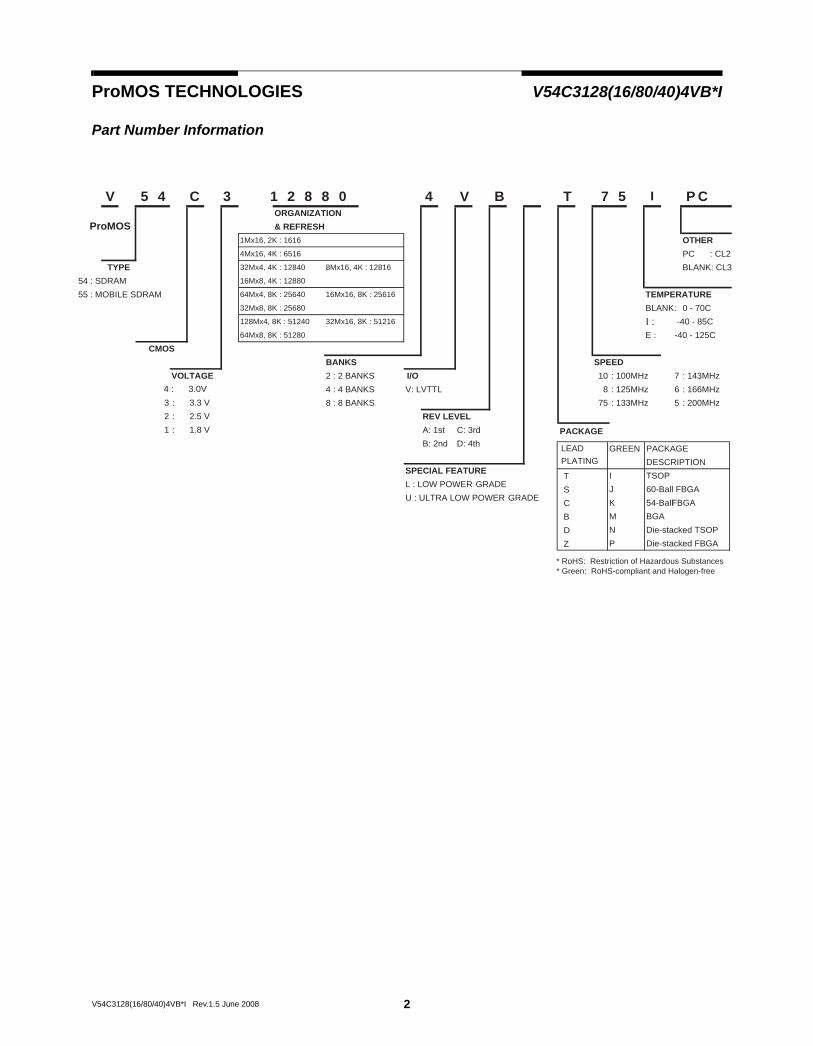
Part Number Information
V 5 4 C 3 1 2 8 8 0 4 V B T 7 5 P CORGANIZATION
ProMOS & REFRESH1Mx16, 2K : 1616 OTHER4Mx16, 4K : 6516 PC : CL2
TYPE 32Mx4, 4K : 12840 8Mx16, 4K : 12816 BLANK: CL354 : SDRAM 16Mx8, 4K : 12880
55 : MOBILE SDRAM 64Mx4, 8K : 25640 16Mx16, 8K : 25616 TEMPERATURE32Mx8, 8K : 25680 BLANK: 0 - 70C128Mx4, 8K : 51240 32Mx16, 8K : 51216 I : -40 - 85C64Mx8, 8K : 51280 E : -40 - 125C
CMOSBANKS SPEED
VOLTAGE 2 : 2 BANKS I/O 10 : 100MHz 7 : 143MHz
3 : 3.3 V4 : 4 BANKS V: LVTTL 8 : 125MHz 6 : 166MHz
2 : 2.5 V8 : 8 BANKS 75 : 133MHz 5 : 200MHz
1 : 1.8 VREV LEVELA: 1st C: 3rd PACKAGEB: 2nd D: 4th LEAD GREEN PACKAGE
PLATING DESCRIPTIONSPECIAL FEATURE T I TSOPL : LOW POWER GRADE S J 60-Ball FBGAU : ULTRA LOW POWER GRADE C K 54-Ball FBGA
B M BGAD N Die-stacked TSOPZ P Die-stacked FBGA
4 : 3.0V
* RoHS: Restriction of Hazardous Substances* Green: RoHS-compliant and Halogen-free
I
3V54C3128(16/80/40)4VB*I Rev. 1.5 June 2008
ProMOS TECHNOLOGIES V54C3128(16/80/40)4VB*I
Description Pkg. Pin Count
1 2 3 7 8 9
VSS VSSQ A VDDQ VDD
DQ3 VDDQ B VSSQ DQ0
VSSQ C VDDQ
DQ2 VDDQ D VSSQ DQ1
NC VSS E VDD
CLK CKE F CAS RAS WE
NC A11 A9 G BA0 BA1 CS
A8 A7 A6 H A0 A1 A10
VSS A5 A4 J A3 A2 VDD
1 2 3 7 8 9
VSS DQ15 VSSQ A VDDQ DQ0 VDD
DQ14 DQ13 VDDQ B VSSQ DQ2 DQ1
DQ12 DQ11 VSSQ C VDDQ DQ4 DQ3
DQ10 DQ9 VDDQ D VSSQ DQ6 DQ5
DQ8 NC VSS E VDD LDQM DQ7
UDQM CLK CKE F CAS RAS WE
NC A11 A9 G BA0 BA1 CS
A8 A7 A6 H A0 A1 A10
VSS A5 A4 J A3 A2 VDD
1 2 3 7 8 9
VSS DQ7 VSSQ A VDDQ DQ0 VDD
NC DQ6 VDDQ B VSSQ DQ1 NC
DQ5 VSSQ C VDDQ DQ2
DQ4 VDDQ D VSSQ DQ3
NC VSS E VDD
CLK CKE F CAS RAS WE
NC A11 A9 G BA0 BA1 CS
A8 A7 A6 H A0 A1 A10
VSS A5 A4 J A3 A2 VDD
X4 devices
X16 devices
X8 devices
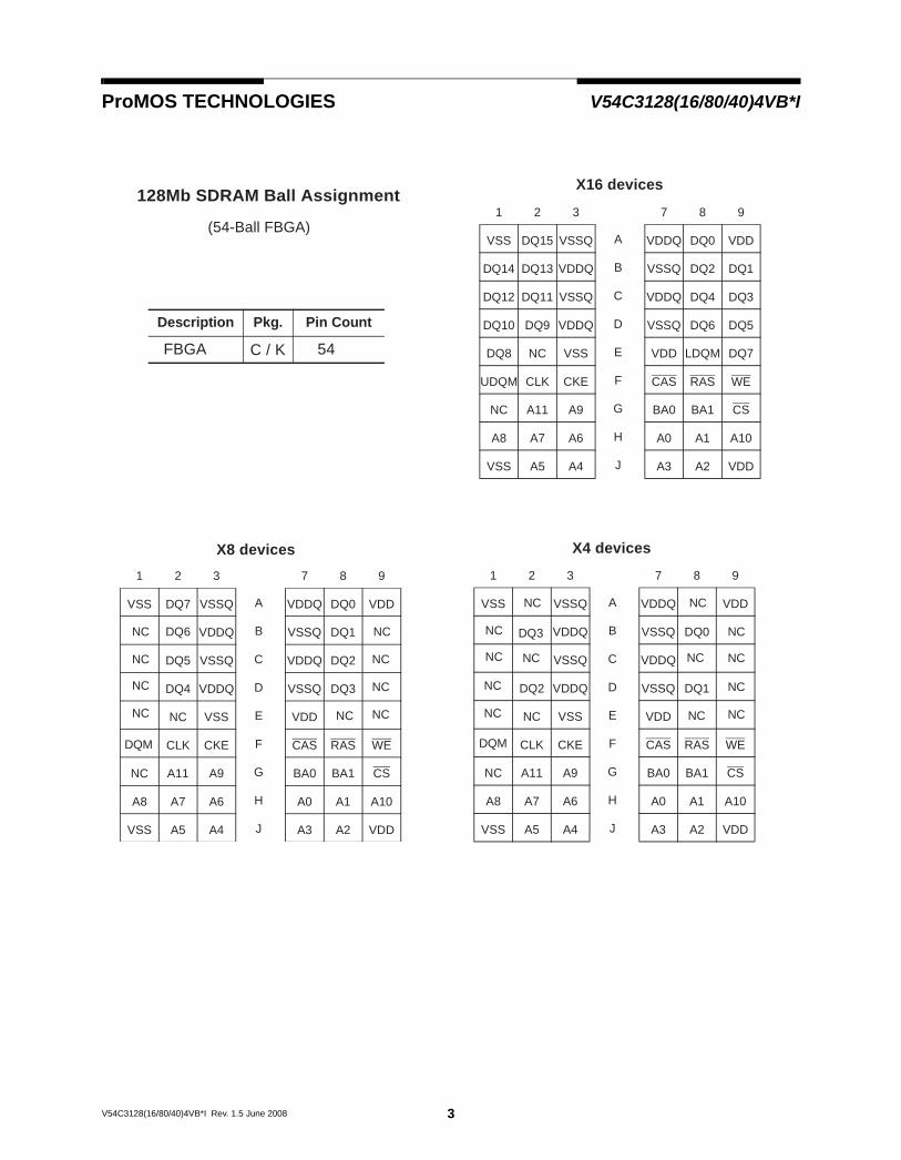
FBGA C / K 54
128Mb SDRAM Ball Assignment
NC
NC
NC
DQM
NC
NC
NC
NC
NC
NC
NC
NC
DQM
NC
NC
NC
NC
NC
NC
NC
NC
NC
(54-Ball FBGA)

4V54C3128(16/80/40)4VB*I Rev. 1.5 June 2008
ProMOS TECHNOLOGIES V54C3128(16/80/40)4VB*I
60 Pin WBGA PIN CONFIGURATIONTop View
Description Pkg. Pin Count
FBGA S / J 60
DQ10
VDDQ
NC
NC
NC
NC
NC
A11
VDDQ
DQ11
A8
A6
A4
VSSQ
DQ9
DQ8
VSS
UDQM
CLK
CKE
A9
VSSQ
DQ13
DQ12
A7
A5
VSS
ABCDEFGHJKLMNPR
DQ14
DQ15 VSS
NC
VDDQ
NC
NC
NC
NC
NC
A11
VDDQ
DQ5
A8
A6
A4
VSSQ
DQ4
NC
VSS
DQM
CLK
CKE
A9
VSSQ
DQ6
NC
A7
A5
VSS
NC
DQ7 VSS
1 2 1 2X16 X8
NC
VDDQ
NC
NC
NC
NC
NC
A11
VDDQ
NC
A8
A6
A4
VSSQ
DQ2
NC
VSS
DQM
CLK
CKE
A9
VSSQ
DQ3
NC
A7
A5
VSS
NC
NC VSS
1 2X4
VDDQ
DQ1
NC
VDD
WE#
RAS#
NC
BA1
DQ0
NC
A0
A2
VDD
NC
VSSQ
NC
NC
CAS#
NC
CS#
BA0
NC
VSSQ
NC
A10
A1
A3
VDDQ
VDD NC
7 8X4
VDDQ
DQ3
NC
VDD
WE#
RAS#
NC
BA1
DQ1
NC
A0
A2
VDD
NC
VSSQ
NC
NC
CAS#
NC
CS#
BA0
NC
VSSQ
DQ2
A10
A1
A3
VDDQ
VDD DQ0
7 8X8
VDDQ
DQ6
DQ7
VDD
WE#
RAS#
NC
BA1
DQ2
DQ3
A0
A2
VDD
DQ5
VSSQ
NC
LDQM
CAS#
NC
CS#
BA0
DQ1
VSSQ
DQ4
A10
A1
A3
VDDQ
VDD DQ0
7 8X16
ABCDEFGHJKLMNPR
TOP VIEW
(60-Ball TrueCSP)128 Mb SDRAM Ball Assignment
PIN A1 index
128Mb SDRAM Ball Assignment
(60-Ball FBGA)
5V54C3128(16/80/40)4VB*I Rev. 1.5 June 2008
ProMOS TECHNOLOGIES V54C3128(16/80/40)4VB*I
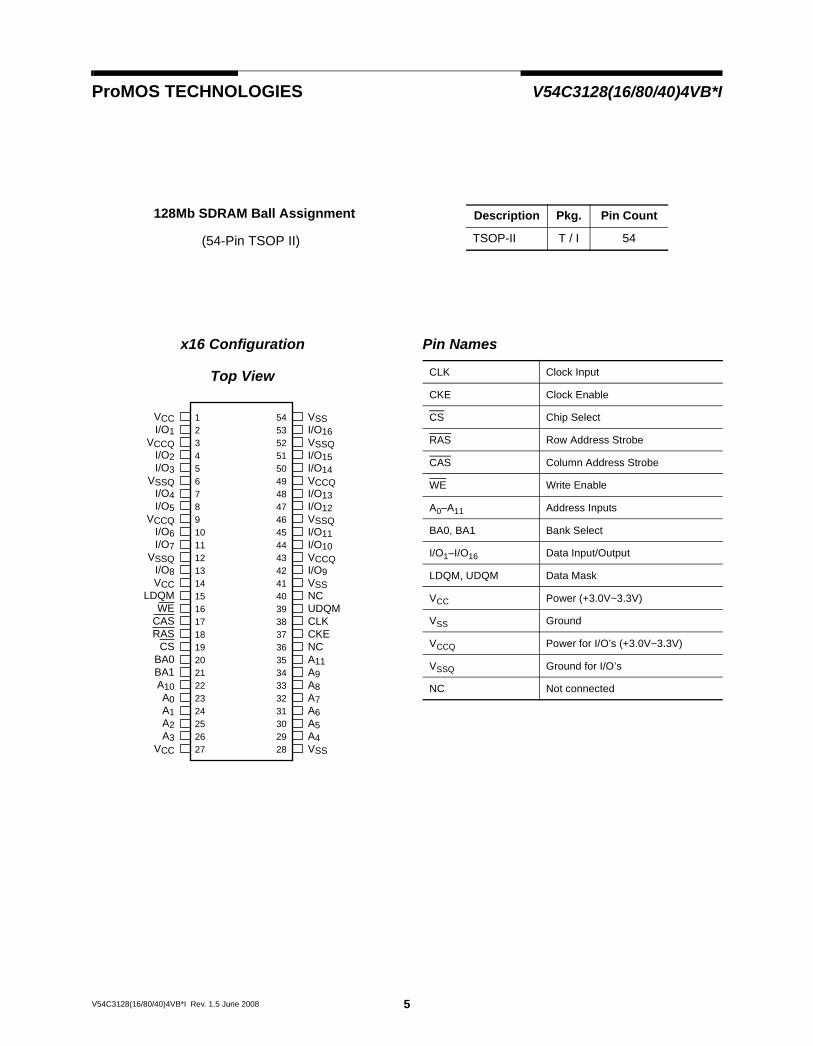
x16 Configuration
Top View
Pin Names
VCCI/O1
VCCQI/O2I/O3
VSSQI/O4I/O5
VCCQI/O6I/O7
VSSQI/O8VCC
LDQMWE
CASRAS
CSBA0BA1A10A0A1A2A3
VCC
VSSI/O16VSSQI/O15I/O14VCCQI/O13I/O12VSSQI/O11I/O10VCCQI/O9VSSNCUDQMCLKCKENCA11A9A8A7A6A5A4VSS
123456789101112131415161718192021222324252627
545352515049484746454443424140393837363534333231302928
CLK Clock Input
CKE Clock Enable
CS Chip Select
RAS Row Address Strobe
CAS Column Address Strobe
WE Write Enable
A0–A11 Address Inputs
BA0, BA1 Bank Select
I/O1–I/O16 Data Input/Output
LDQM, UDQM Data Mask
VCC Power (+3.0V~3.3V)
VSS Ground
VCCQ Power for I/O’s (+3.0V~3.3V)
VSSQ Ground for I/O’s
NC Not connected
Description Pkg. Pin Count
TSOP-II T / I 54
128Mb SDRAM Ball Assignment
(54-Pin TSOP II)
6V54C3128(16/80/40)4VB*I Rev.1.5 June 2008
ProMOS TECHNOLOGIES V54C3128(16/80/40)4VB*I
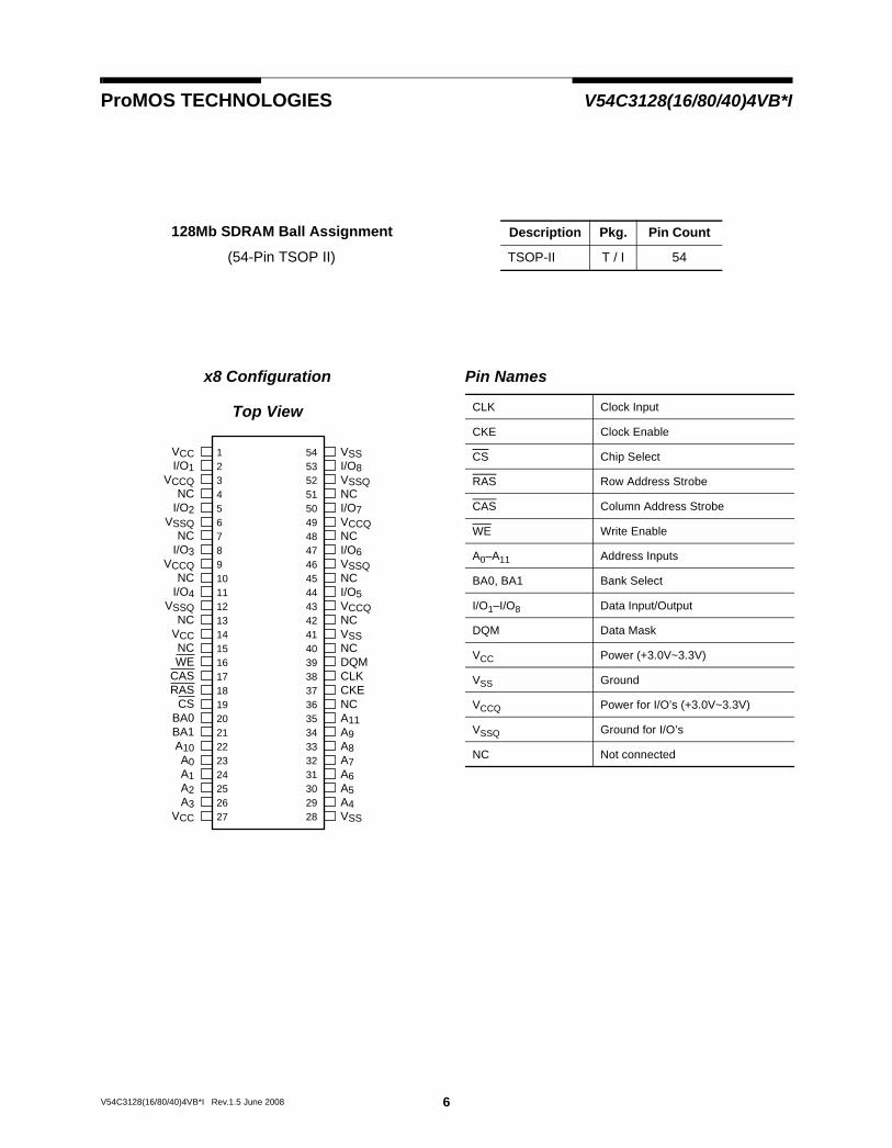
x8 Configuration
Top View
Pin Names
VCCI/O1
VCCQNC
I/O2VSSQ
NCI/O3
VCCQNC
I/O4VSSQ
NCVCCNCWE
CASRAS
CSBA0BA1A10A0A1A2A3
VCC
VSSI/O8VSSQNCI/O7VCCQNCI/O6VSSQNCI/O5VCCQNCVSSNCDQMCLKCKENCA11A9A8A7A6A5A4VSS
123456789101112131415161718192021222324252627
545352515049484746454443424140393837363534333231302928
CLK Clock Input
CKE Clock Enable
CS Chip Select
RAS Row Address Strobe
CAS Column Address Strobe
WE Write Enable
A0–A11 Address Inputs
BA0, BA1 Bank Select
I/O1–I/O8 Data Input/Output
DQM Data Mask
VCC Power (+3.0V~3.3V)
VSS Ground
VCCQ Power for I/O’s (+3.0V~3.3V)
VSSQ Ground for I/O’s
NC Not connected
Description Pkg. Pin Count
TSOP-II T / I 54
128Mb SDRAM Ball Assignment
(54-Pin TSOP II)

7V54C3128(16/80/40)4VB*I Rev. 1.5 June 2008
ProMOS TECHNOLOGIES V54C3128(16/80/40)4VB*I
x4 Configuration
Top View
Pin Names
VCCNC
VCCQNC
I/O1VSSQ
NCNC
VCCQNC
I/O2VSSQ
NCVCCNCWE
CASRAS
CSBA0BA1A10A0A1A2A3
VCC
VSSNCVSSQNCI/O4VCCQNCNCVSSQNCI/O3VCCQNCVSSNCDQMCLKCKENCA11A9A8A7A6A5A4VSS
123456789101112131415161718192021222324252627
545352515049484746454443424140393837363534333231302928
CLK Clock Input
CKE Clock Enable
CS Chip Select
RAS Row Address Strobe
CAS Column Address Strobe
WE Write Enable
A0–A11 Address Inputs
BA0, BA1 Bank Select
I/O1–I/O4 Data Input/Output
DQM Data Mask
VCC Power (+3.0V~3.3V)
VSS Ground
VCCQ Power for I/O’s (+3.0V~3.3V)
VSSQ Ground for I/O’s
NC Not connected
Description Pkg. Pin Count
TSOP-II T / I 54
128Mb SDRAM Ball Assignment
(54-Pin TSOP II)

ProMOS TECHNOLOGIES V54C3128(16/80/40)4VB*I
Capacitance*TA = -40 to +85°C, VCC = (3.0V~3.3 V) ± 0.3 V, f =1 Mhz
*Note:Capacitance is sampled and not 100% tested.
Absolute Maximum Ratings*Operating temperature range .............-40 to +85 °CStorage temperature range ................-55 to 150 °CInput/output voltage.................. -0.3 to (VCC+0.3) VPower supply voltage .......................... -0.3 to 4.6 VPower dissipation ..............................................1 WData out current (short circuit).......................50 mA
*Note: Stresses above those listed under “Absolute Maximum Ratings” may cause permanent damage of the device. Exposure to absolute maximum rating conditions for extended periods may affect device reliability.
Symbol Parameter Max. Unit
CI1 Input Capacitance (A0 to A11) 3.8 pF
CI2 Input Capacitance RAS, CAS, WE, CS, CLK, CKE, DQM
3.8 pF
CIO Output Capacitance (I/O) 6 pF
CCLK Input Capacitance (CLK) 3.5 pF
8V54C3128(16/80/40)4VB*I Rev. 1.5 June 2008
Block Diagram
Row decoder
Memory array
Bank 0
4096 x 512x 16 bit
Col
umn
deco
der
Sen
se a
mpl
ifier
& I(
O) b
us
Row decoder
Memory array
Bank 1
4096 x 512x16 bit
Col
umn
deco
der
Sen
se a
mpl
ifier
& I(
O) b
us
Row decoder
Memory array
Bank 2
4096 x 512x 16 bit
Col
umn
deco
der
Sen
se a
mpl
ifier
& I(
O) b
us
Row decoder
Memory array
Bank 3
4096 x 512x 16 bit
Col
umn
deco
der
Sen
se a
mpl
ifier
& I(
O) b
us
Input buffer Output buffer
I/O1-I/O16
Column addresscounter
Column addressbuffer
Row address buffer Refresh Counter
A0 - A11, BA0, BA1A0 - A8, AP, BA0, BA1
Control logic & timing generator
CLK
CK
E
CS
RA
S
CA
S
WE
LDQ
M
Row AddressesColumn Addresses
UD
QM
x16 Configuration
9V54C3128(16/80/40)4VB*I Rev. 1.5 June 2008
ProMOS TECHNOLOGIES V54C3128(16/80/40)4VB*I
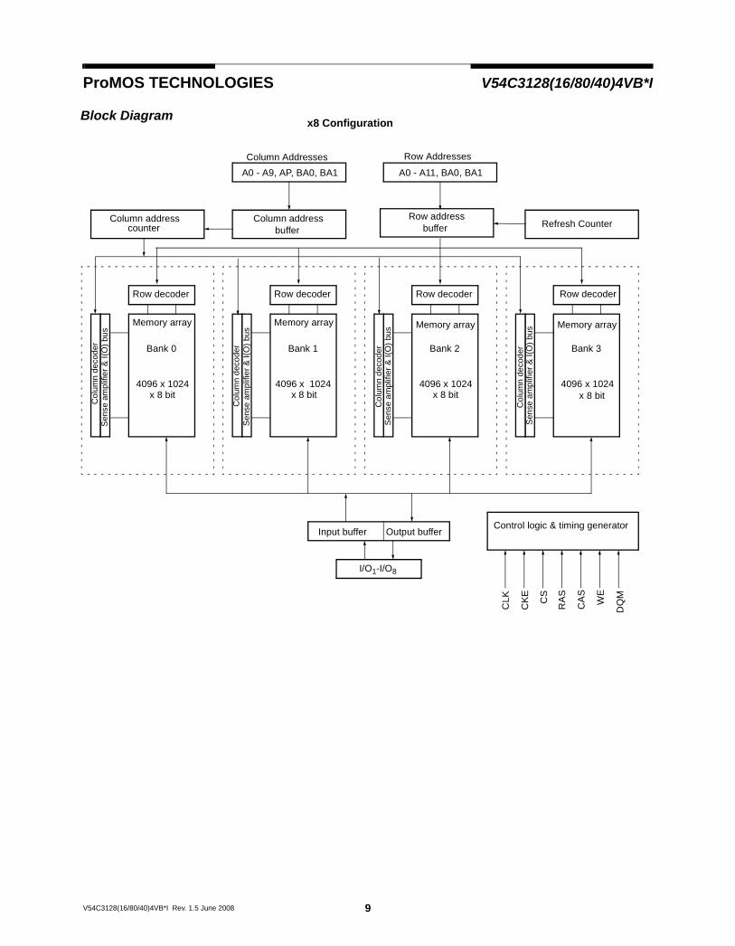
Block Diagram x8 Configuration
Row decoder
Memory array
Bank 0
4096 x 1024x 8 bit
Col
umn
deco
der
Sen
se a
mpl
ifier
& I(
O) b
us
Row decoder
Memory array
Bank 1
4096 x 1024x 8 bit
Col
umn
deco
der
Sen
se a
mpl
ifier
& I(
O) b
us
Row decoder
Memory array
Bank 2
4096 x 1024x 8 bit
Col
umn
deco
der
Sen
se a
mpl
ifier
& I(
O) b
us
Row decoder
Memory array
Bank 3
4096 x 1024x 8 bit
Col
umn
deco
der
Sen
se a
mpl
ifier
& I(
O) b
usInput buffer Output buffer
I/O1-I/O8
Column addresscounter
Column addressbuffer
Row address buffer Refresh Counter
A0 - A11, BA0, BA1A0 - A9, AP, BA0, BA1
Control logic & timing generator
CLK
CK
E
CS
RA
S
CA
S
WE
DQ
M
Row AddressesColumn Addresses

10V54C3128(16/80/40)4VB*I Rev.1.5 June 2008
ProMOS TECHNOLOGIES V54C3128(16/80/40)4VB*I
Block Diagram x4 Configuration
Row decoder
Memory array
Bank 0
4096 x 2048x 4 bit
Col
umn
deco
der
Sen
se a
mpl
ifier
& I(
O) b
us
Row decoder
Memory array
Bank 1
4096 x 2048x 4 bit
Col
umn
deco
der
Sen
se a
mpl
ifier
& I(
O) b
us
Row decoder
Memory array
Bank 2
4096 x 2048x 4 bit
Col
umn
deco
der
Sen
se a
mpl
ifier
& I(
O) b
us
Row decoder
Memory array
Bank 3
4096 x 2048x 4 bit
Col
umn
deco
der
Sen
se a
mpl
ifier
& I(
O) b
usInput buffer Output buffer
I/O1-I/O4
Column addresscounter
Column addressbuffer
Row address buffer Refresh Counter
A0 - A11, BA0, BA1A0 - A9, A11, AP, BA0, BA1
Control logic & timing generatorC
LK
CK
E
CS
RA
S
CA
S
WE
DQ
M
Row AddressesColumn Addresses

ProMOS TECHNOLOGIES V54C3128(16/80/40)4VB*I
Signal Pin Description
Pin Type Signal Polarity Function
CLK Input Pulse Positive Edge
The system clock input. All of the SDRAM inputs are sampled on the rising edge of the clock.
CKE Input Level Active High Activates the CLK signal when high and deactivates the CLK signal when low, thereby initiates either the Power Down mode or the Self Refresh mode.
CS Input Pulse Active Low CS enables the command decoder when low and disables the command decoder when high. When the command decoder is disabled, new commands are ignored but previous operations continue.
RAS, CAS WE
Input Pulse Active Low When sampled at the positive rising edge of the clock, CAS, RAS, and WE define the command to be executed by the SDRAM.
A0 - A11 Input Level — During a Bank Activate command cycle, A0-A11 defines the row address (RA0-RA11) when sampled at the rising clock edge. During a Read or Write command cycle, A0-An defines the column address (CA0-CAn) when sampled at the rising clock edge.CAn depends from the SDRAM organization:• 32M x 4 SDRAM CA0–CA9, CA11.• 16M x 8 SDRAM CA0–CA9. • 8M x 16 SDRAM CA0–CA8.
In addition to the column address, A10(=AP) is used to invoke autoprecharge operation at the end of the burst read or write cycle. If A10 is high, autoprecharge is selected and BA0, BA1 defines the bank to be precharged. If A10 is low, autoprecharge is disabled.During a Precharge command cycle, A10(=AP) is used in conjunction with BA0 and BA1 to control which bank(s) to precharge. If A10 is high, all four banks will BA0 and BA1 are used to define which bank to precharge.
BA0,BA1
Input Level — Selects which bank is to be active.
DQx InputOutput
Level — Data Input/Output pins operate in the same manner as on conventional DRAMs.
LDQMUDQM
Input Pulse Active High The Data Input/Output mask places the DQ buffers in a high impedance state when sam-pled high. In Read mode, DQM has a latency of two clock cycles and controls the output buffers like an output enable. In Write mode, DQM has a latency of zero and operates as a word mask by allowing input data to be written if it is low but blocks the write operation if DQM is high.
VCC, VSS Supply Power and ground for the input buffers and the core logic.
VCCQ VSSQ
Supply — — Isolated power supply and ground for the output buffers to provide improved noise immunity.
11V54C3128(16/80/40)4VB*I Rev. 1.5 June 2008

ProMOS TECHNOLOGIES V54C3128(16/80/40)4VB*I
Operation DefinitionAll of SDRAM operations are defined by states of control signals CS, RAS, CAS, WE, and DQM at the
positive edge of the clock. The following list shows the thruth table for the operation commands.
Notes:1. V = Valid , x = Don’t Care, L = Low Level, H = High Level2. CKEn signal is input level when commands are provided, CKEn-1 signal is input level one clock before the commands
are provided.3. These are state of bank designated by BS0, BS1 signals.4. Power Down Mode can not entry in the burst cycle.
OperationDeviceState
CKEn-1
CKEn CS RAS CAS WE DQM
A0-9, A11 A10
BS0BS1
Row Activate Idle3 H X L L H H X V V V
Read Active3 H X L H L H X V L V
Read w/Autoprecharge Active3 H X L H L H X V H V
Write Active3 H X L H L L X V L V
Write with Autoprecharge Active3 H X L H L L X V H V
Row Precharge Any H X L L H L X X L V
Precharge All Any H X L L H L X X H X
Mode Register Set Idle H X L L L L X V V V
No Operation Any H X L H H H X X X X
Device Deselect Any H X H X X X X X X X
Auto Refresh Idle H H L L L H X X X X
Self Refresh Entry Idle H L L L L H X X X X
Self Refresh Exit Idle(Self Refr.) L H
H X X XX X X X
L H H X
Power Down Entry IdleActive4 H L
H X X XX X X X
L H H X
Power Down Exit Any(Power Down)
L HH X X X
X X X XL H H L
Data Write/Output Enable Active H X X X X X L X X X
Data Write/Output Disable Active H X X X X X H X X X
12V54C3128(16/80/40)4VB*I Rev.1.5 June 2008

ProMOS TECHNOLOGIES V54C3128(16/80/40)4VB*I
Power On and InitializationThe default power on state of the mode register is
supplier specific and may be undefined. Thefollowing power on and initialization sequenceguarantees the device is preconditioned to eachusers specific needs. Like a conventional DRAM,the Synchronous DRAM must be powered up andinitialized in a predefined manner. During power on,all VCC and VCCQ pins must be built upsimultaneously to the specified voltage when theinput signals are held in the “NOP” state. The poweron voltage must not exceed VCC+0.3V on any ofthe input pins or VCC supplies. The CLK signalmust be started at the same time. After power on,an initial pause of 200 µs is required followed by aprecharge of both banks using the prechargecommand. To prevent data contention on the DQbus during power on, it is required that the DQM andCKE pins be held high during the initial pauseperiod. Once all banks have been precharged, theMode Register Set Command must be issued toinitialize the Mode Register. A minimum of eightAuto Refresh cycles (CBR) are also required.Thesemay be done before or after programming the ModeRegister. Failure to follow these steps may lead tounpredictable start-up modes.
Programming the Mode RegisterThe Mode register designates the operation
mode at the read or write cycle. This register is di-vided into 4 fields. A Burst Length Field to set thelength of the burst, an Addressing Selection bit toprogram the column access sequence in a burst cy-cle (interleaved or sequential), a CAS Latency Fieldto set the access time at clock cycle and a Opera-tion mode field to differentiate between normal op-eration (Burst read and burst Write) and a specialBurst Read and Single Write mode. The mode setoperation must be done before any activate com-mand after the initial power up. Any content of themode register can be altered by re-executing the
mode set command. All banks must be in pre-charged state and CKE must be high at least oneclock before the mode set operation. After the moderegister is set, a Standby or NOP command is re-quired. Low signals of RAS, CAS, and WE at thepositive edge of the clock activate the mode set op-eration. Address input data at this timing defines pa-rameters to be set as shown in the previous table.
Read and Write OperationWhen RAS is low and both CAS and WE are high
at the positive edge of the clock, a RAS cycle starts.According to address data, a word line of the select-ed bank is activated and all of sense amplifiers as-sociated to the wordline are set. A CAS cycle istriggered by setting RAS high and CAS low at aclock timing after a necessary delay, tRCD, from theRAS timing. WE is used to define either a read(WE = H) or a write (WE = L) at this stage.
SDRAM provides a wide variety of fast accessmodes. In a single CAS cycle, serial data read orwrite operations are allowed at up to a 125 MHzdata rate. The numbers of serial data bits are theburst length programmed at the mode set operation,i.e., one of 1, 2, 4, 8 and full page. Column address-es are segmented by the burst length and serialdata accesses are done within this boundary. Thefirst column address to be accessed is supplied atthe CAS timing and the subsequent addresses aregenerated automatically by the programmed burstlength and its sequence. For example, in a burstlength of 8 with interleave sequence, if the first ad-dress is ‘2’, then the rest of the burst sequence is 3,0, 1, 6, 7, 4, and 5.
Full page burst operation is only possible usingsequential burst type. Full Page burst operationdoes not terminate once the burst length has beenreached. (At the end of the page, it will wrap to thestart address and continue.) In other words, unlikeburst length of 2, 4, and 8, full page burst continuesuntil it is terminated using another command.
13V54C3128(16/80/40)4VB*I Rev. 1.5 June 2008

ProMOS TECHNOLOGIES V54C3128(16/80/40)4VB*I
Address Input for Mode Set (Mode Register Operation)
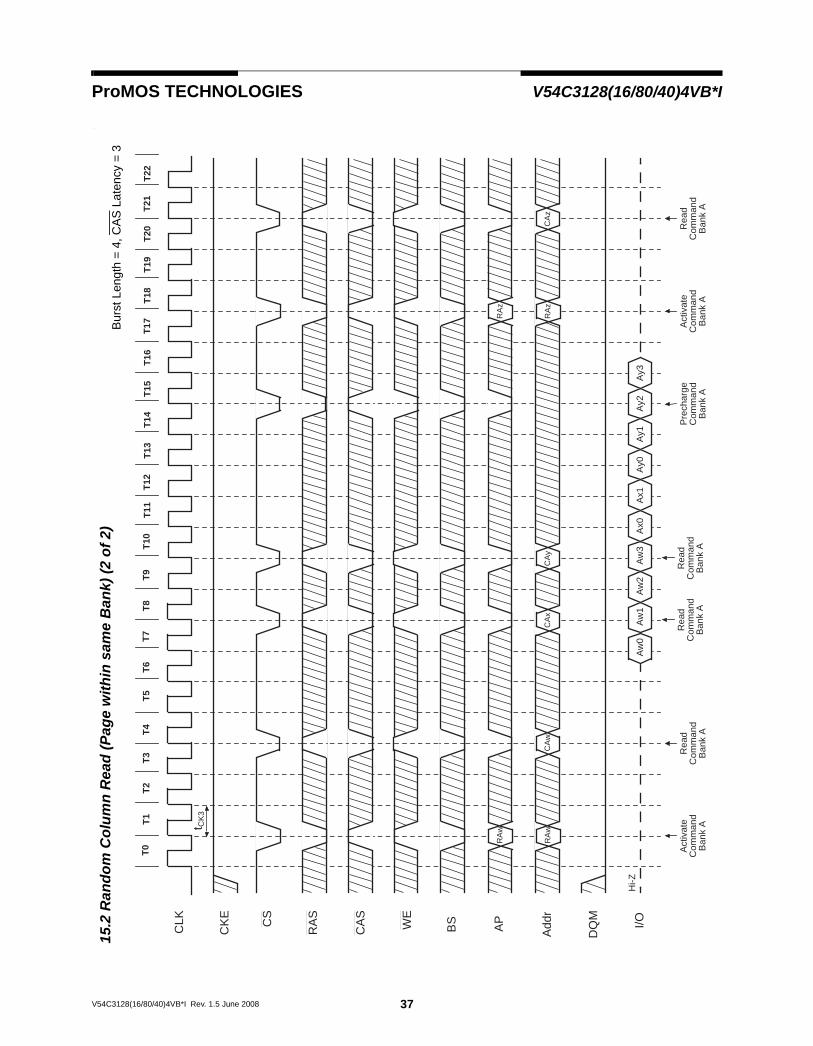
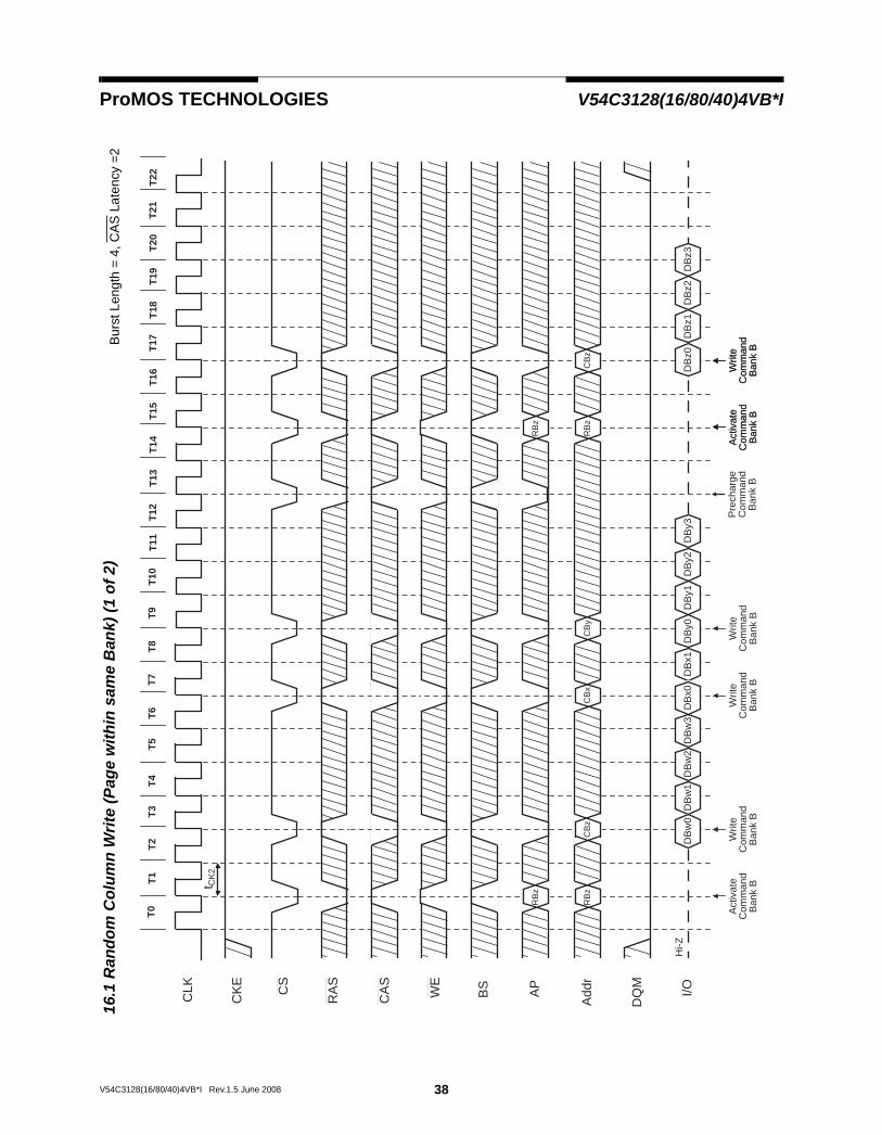
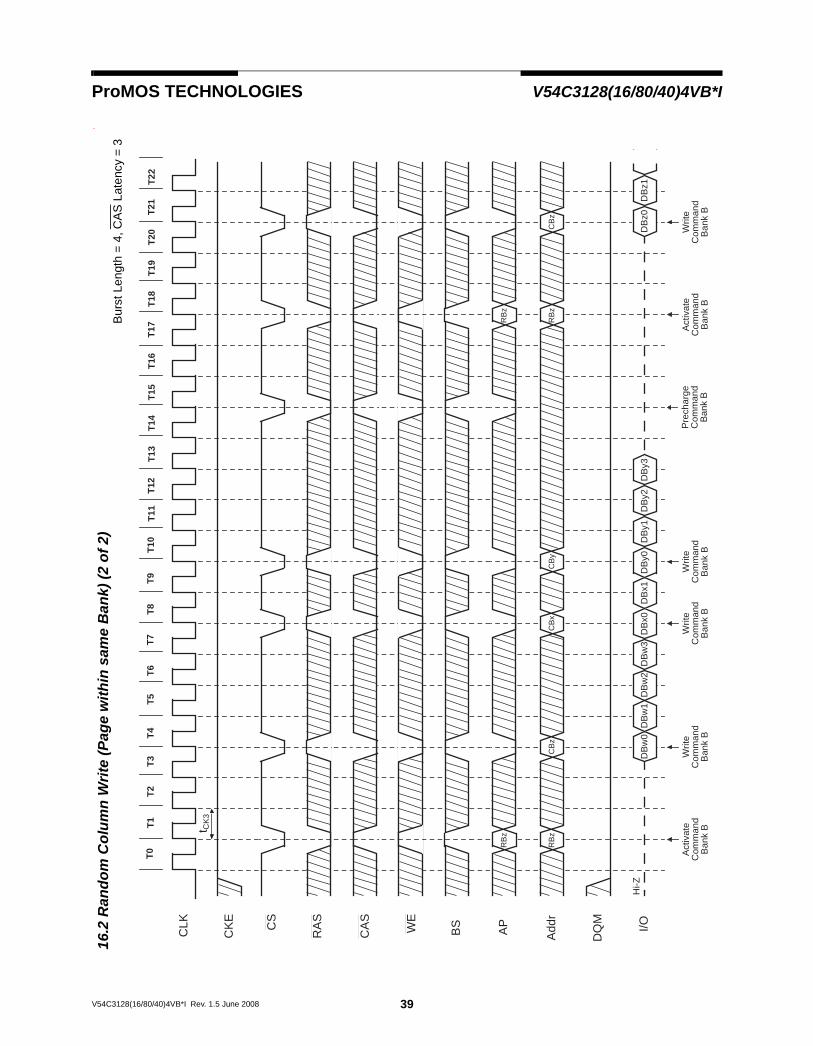
Similar to the page mode of conventionalDRAM’s, burst read or write accesses on any col-umn address are possible once the RAS cyclelatches the sense amplifiers. The maximum tRAS orthe refresh interval time limits the number of randomcolumn accesses. A new burst access can be doneeven before the previous burst ends. The interruptoperation at every clock cycles is supported. Whenthe previous burst is interrupted, the remaining ad-dresses are overridden by the new address with thefull burst length. An interrupt which accompanieswith an operation change from a read to a write ispossible by exploiting DQM to avoid bus contention.
When two or more banks are activatedsequentially, interleaved bank read or writeoperations are possible. With the programmedburst length, alternate access and prechargeoperations on two or more banks can realize fastserial data access modes among many differentpages. Once two or more banks are activated,column to column interleave operation can be donebetween different pages.
A11 A3A4 A2 A1 A0A10 A9 A8 A7 A6 A5 Address Bus (Ax)
BT Burst LengthCAS Latency Mode Register
CAS Latency
A6 A5 A4 Latency
0 0 0 Reserve
0 0 1 Reserve
0 1 0 2
0 1 1 3
1 0 0 Reserve
1 0 1 Reserve
1 1 0 Reserve
1 1 1 Reserve
Burst Length
A2 A1 A0Length
Sequential Interleave
0 0 0 1 1
0 0 1 2 2
0 1 0 4 4
0 1 1 8 8
1 0 0 Reserve Reserve
1 0 1 Reserve Reserve
1 1 0 Reserve Reserve
1 1 1 Full Page Reserve
Burst Type
A3 Type
0 Sequential
1 Interleave
Operation Mode
BA1 BA0 A11 A10 A9 A8 A7 Mode
0 0 0 0 0 0 0 Burst Read/Burst Write
0 0 0 0 1 0 0 Burst Read/Single Write
Operation Mode
BA0BA1
14V54C3128(16/80/40)4VB*I Rev.1.5 June 2008

ProMOS TECHNOLOGIES V54C3128(16/80/40)4VB*I
Burst Length and Sequence:Burst Length
Starting Address
(A2 A1 A0)
Sequential Burst Addressing
(decimal)
Interleave Burst Addressing(decimal)
2 xx0xx1
0, 11, 0
0, 11, 0
4 x00x01x10x11
0, 1, 2, 31, 2, 3, 02, 3, 0, 13, 0, 1, 2
0, 1, 2, 31, 0, 3, 22, 3, 0, 13, 2, 1, 0
8 000001010011100101110111
0 1 2 3 4 5 6 7 1 2 3 4 5 6 7 0 2 3 4 5 6 7 0 1 3 4 5 6 7 0 1 2 4 5 6 7 0 1 2 3 5 6 7 0 1 2 3 4 6 7 0 1 2 3 4 5 7 0 1 2 3 4 5 6
0 1 2 3 4 5 6 7 1 0 3 2 5 4 7 6 2 3 0 1 6 7 4 5 3 2 1 0 7 6 5 4 4 5 6 7 0 1 2 3 5 4 7 6 1 0 3 2 6 7 4 5 2 3 0 1 7 6 5 4 3 2 1 0
Full Page nnn Cn, Cn+1, Cn+2.... not supported
Refresh ModeSDRAM has two refresh modes, Auto Refresh and Self Refresh. Auto Refresh is similar to the CAS -before-
RAS refresh of conventional DRAMs. All of banks must be precharged before applying any refresh mode. Anon-chip address counter increments the word and the bank addresses and no bank information is requiredfor both refresh modes.
The chip enters the Auto Refresh mode, when RAS and CAS are held low and CKE and WE are held highat a clock timing. The mode restores word line after the refresh and no external precharge command is nec-essary. A minimum tRC time is required between two automatic refreshes in a burst refresh mode. The samerule applies to any access command after the automatic refresh operation.
The chip has an on-chip timer and the Self Refresh mode is available. It enters the mode when RAS, CAS,and CKE are low and WE is high at a clock timing. All of external control signals including the clock are dis-abled. Returning CKE to high enables the clock and initiates the refresh exit operation. After the exit com-mand, at least one tRC delay is required prior to any access command.
DQM FunctionDQM has two functions for data I/O read and write operations. During reads, when it turns to “high” at a
clock timing, data outputs are disabled and become high impedance after two clock delay (DQM Data DisableLatency tDQZ ). It also provides a data mask function for writes. When DQM is activated, the write operationat the next clock is prohibited (DQM Write Mask Latency tDQW = zero clocks).
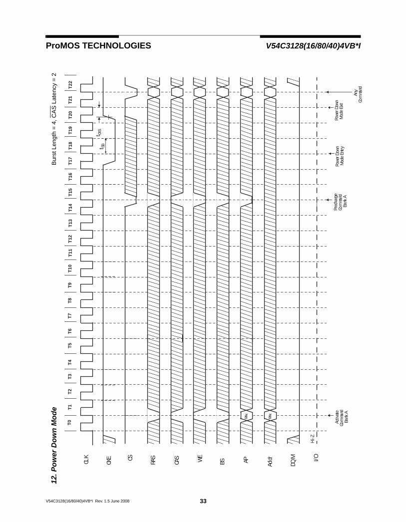
Power DownIn order to reduce standby power consumption, a power down mode is available. All banks must be pre-
charged and the necessary Precharge delay (trp) must occur before the SDRAM can enter the Power Downmode. Once the Power Down mode is initiated by holding CKE low, all of the receiver circuits except CLKand CKE are gated off. The Power Down mode does not perform any refresh operations, therefore the devicecan’t remain in Power Down mode longer than the Refresh period (tref) of the device. Exit from this mode isperformed by taking CKE “high”. One clock delay is required for mode entry and exit.
15V54C3128(16/80/40)4VB*I Rev. 1.5 June 2008

ProMOS TECHNOLOGIES V54C3128(16/80/40)4VB*I
Auto PrechargeTwo methods are available to precharge SDRAMs. In an automatic precharge mode, the CAS timing ac-
cepts one extra address, CA10, to determine whether the chip restores or not after the operation. If CA10 ishigh when a Read Command is issued, the Read with Auto-Precharge function is initiated. The SDRAMautomatically enters the precharge operation one clock before the last data out for CAS latencies 2, twoclocks for CAS latencies 3 and three clocks for CAS latencies 4. If CA10 is high when a Write Command isissued, the Write with Auto-Precharge function is initiated. The SDRAM automatically enters the prechargeoperation a time delay equal to tWR (Write recovery time) after the last data in. Auto-Precharge does notapply to full-page burst mode.
Precharge CommandThere is also a separate precharge command available. When RAS and WE are low and CAS is high at a
clock timing, it triggers the precharge operation. Three address bits, BA0, BA1 and A10 are used to definebanks as shown in the following list. The precharge command can be imposed one clock before the last dataout for CAS latency = 2, two clocks before the last data out for CAS latency = 3. Writes require a time delaytwr from the last data out to apply the precharge command. A full-page burst may be truncated with a Pre-charge command to the same bank.
Bank Selection by Address Bits:
Burst TerminationOnce a burst read or write operation has been initiated, there are several methods in which to terminate
the burst operation prematurely. These methods include using another Read or Write Command to interruptan existing burst operation, use a Precharge Command to interrupt a burst cycle and close the active bank,or using the Burst Stop Command to terminate the existing burst operation but leave the bank open for futureRead or Write Commands to the same page of the active bank. When interrupting a burst with another Reador Write Command care must be taken to avoid I/O contention. The Burst Stop Command, however, has thefewest restrictions making it the easiest method to use when terminating a burst operation before it has beencompleted. If a Burst Stop command is issued during a burst write operation, then any residual data from theburst write cycle will be ignored. Data that is presented on the I/O pins before the Burst Stop Command isregistered will be written to the memory. The full-page burst is used in conjunction with Burst Terminate Com-mand to generate arbitrary burst lengths.
A10 BA0 BA1
0 0 0 Bank 0
0 0 1 Bank 1
0 1 0 Bank 2
0 1 1 Bank 3
1 X X all Banks
16V54C3128(16/80/40)4VB*I Rev.1.5 June 2008

ProMOS TECHNOLOGIES V54C3128(16/80/40)4VB*I
Recommended Operation and Characteristics for LV-TTLTA = -40 to +85 °C; VSS = 0 V; VCC,VCCQ = (+3.0V~3.3 V) ± 0.3 V
Note:1. All voltages are referenced to VSS. 2. VIH may overshoot to VCC + 2.0 V for pulse width of < 4ns with 3.3V. VIL may undershoot to -2.0 V for pulse width < 4.0 ns with
3.3V. Pulse width measured at 50% points with amplitude measured peak to DC reference.
Operating Currents (TA = -40 to +85°C, VCC = (+3.0V~3.3V) ± 0.3V)(Recommended Operating Conditions unless otherwise noted)
Parameter Symbol
Limit Values
Unit Notesmin. max.
Input high voltage VIH 2.0 Vcc+0.3 V 1, 2
Input low voltage VIL – 0.3 0.8 V 1, 2
Output high voltage (IOUT = – 4.0 mA) VOH 2.4 – V
Output low voltage (IOUT = 4.0 mA) VOL – 0.4 V
Input leakage current, any input(0 V < VIN < 3.6 V, all other inputs = 0 V)
II(L) – 5 5 µA
Output leakage current(DQ is disabled, 0 V < VOUT < VCC)
IO(L) – 5 5 µA
Symbol Parameter & Test Condition
Max.
Unit Note-6 -7 / -7PC
ICC1 Operating CurrenttRC = tRCMIN., tRC = tCKMIN.Active-precharge command cycling, without Burst Operation
1 bank operation 135 115 mA 7
ICC2P Precharge Standby Current in Power Down ModeCS =VIH, CKE≤ VIL(max)
tCK = min. 2 2 mA 7
ICC2PS tCK = Infinity 1 1 mA 7
ICC2N Precharge Standby Current in Non-Power Down ModeCS =VIH, CKE≥ VIL(max)
tCK = min. 20 20 mA
ICC2NS tCK = Infinity 10 10 mA
ICC3N No Operating CurrenttCK = min, CS = VIH(min)bank ; active state ( 4 banks)
CKE ≥ VIH(MIN.) 25 25 mA
ICC3P CKE ≤ VIL(MAX.)(Power down mode)
3 3 mA
ICC4 Burst Operating CurrenttCK = minRead/Write command cycling
110 100 mA 7,8
ICC5 Auto Refresh CurrenttCK = minAuto Refresh command cycling
180 160 mA 7
ICC6 Self Refresh CurrentSelf Refresh Mode, CKE≤ 0.2V
1.5 1.5 mA
L-version 0.8 0.8 mANotes:7.These parameters depend on the cycle rate and these values are measured by the cycle rate under the minimum value of tCK and tRC. Input signals are changed one time during tCK.8.These parameter depend on output loading. Specified values are obtained with output open.
17V54C3128(16/80/40)4VB*I Rev. 1.5 June 2008

ProMOS TECHNOLOGIES V54C3128(16/80/40)4VB*I
AC Characteristics 1,2, 3 TA = -40 to +85 °C; VSS = 0 V; VDD = (+3.0V~3.3 V) ± 0.3 V, tT = 1 ns
# Symbol Parameter
Limit Values
Unit Note
-6 -7PC -7
Min. Max. Min. Max. Min. Max.
Clock and Clock Enable
1 tCK Clock Cycle Time CAS Latency = 3CAS Latency = 2
67.5
––
77.5
––
710
––
snsns
2 tCK Clock Frequency CAS Latency = 3CAS Latency = 2
––
166133
––
143133
––
143100
MHzMHz
3 tAC Access Time from ClockCAS Latency = 3CAS Latency = 2
–_
5.45.4
–_
5.45.4
–_
5.46
nsns
2, 4
4 tCH Clock High Pulse Width 2.5 – 2.5 – 2.5 – ns
5 tCL Clock Low Pulse Width 2.5 – 2.5 – 2.5 – ns
6 tT Transition Tim 0.3 1.2 0.3 1.2 0.3 1.2 ns
Setup and Hold Times
7 tIS Input Setup Time 1.5 – 1.5 – 1.5 – ns 5
8 tIH Input Hold Time 0.8 – 0.8 – 0.8 – ns 5
9 tCKS Input Setup Time 1.5 – 1.5 – 1.5 – ns 5
10 tCKH CKE Hold Time 0.8 – 0.8 – 0.8 – ns 5
11 tRSC Mode Register Set-up Time 12 – 14 – 14 – ns
12 tSB Power Down Mode Entry Time 0 6 0 7 0 7 ns
13 tDS Data-in setup time 1.5 – 1.5 – 1.5 – ns
14 tDH Data-in hold time 0.8 – 0.8 – 0.8 – ns
Common Parameters
15 tRCD Row to Column Delay Time 15 – 15 – 15 – ns 6
16 tRP Row Precharge Time 15 – 15 – 15 – ns 6
17 tRAS Row Active Time 40 100K 42 100K 42 100K ns 6
18 tRC Row Cycle Time 60 – 60 – 60 – ns 6
19 tRRD Activate(a) to Activate(b) Command Period 12 – 14 – 14 – ns 6
20 tCCD CAS(a) to CAS(b) Command Period 1 – 1 – 1 – CLK
21 tDPL Data-in to Precharge Command for Manual precharge
2 – 2 – 2 – CLK
Refresh Cycle
22 tREF Refresh Period (4096 cycles) — 64 — 64 — 64 ms
23 tSREX Self Refresh Exit Time 1 — 1 — 1 — CLK
18V54C3128(16/80/40)4VB*I Rev.1.5 June 2008

ProMOS TECHNOLOGIES V54C3128(16/80/40)4VB*I
Notes for AC Parameters:
1. For proper power-up see the operation section of this data sheet.
2. AC timing tests have VIL = 0.8V and VIH = 2.0V with the timing referenced to the 1.4 V crossover point. The transitiontime is measured between VIH and VIL. All AC measurements assume tT = 1ns with the AC output load circuit shownin Figure 1.
4. If clock rising time is longer than 1 ns, a time (tT/2 – 0.5) ns has to be added to this parameter.
5. If tT is longer than 1 ns, a time (tT – 1) ns has to be added to this parameter.
6. These parameter account for the number of clock cycle and depend on the operating frequency of the clock, as follows:
the number of clock cycle = specified value of timing period (counted in fractions as a whole number)
Self Refresh Exit is a synchronous operation and begins on the 2nd positive clock edge after CKE returns high. Self Refresh Exit is not complete until a time period equal to tRC is satisfied once the Self Refresh Exit commandis registered.
7. Referenced to the time which the output achieves the open circuit condition, not to output voltage levels
Read Cycle
24 tOH Data Out Hold Time 2.5 – 3 – 3 – ns 2
25 tLZ Data Out to Low Impedance Time 1 – 1 – 1 – ns
26 tHZ Data Out to High Impedance Time 3 6 3 7 3 7 ns 7
27 tDQZ DQM Data Out Disable Latency – 2 – 2 – 2 CLK
Write Cycle
28 tWR Write Recovery Time for Auto precharge 2 – 2 – 2 – CLK
29 tDQW DQM Write Mask Latency 0 – 0 – 0 – CLK
# Symbol Parameter
Limit Values
Unit Note
-6 -7PC -7
Min. Max. Min. Max. Min. Max.
1.4V
1.4V
tIS tIH
tAC tACtLZ tOH
tHZ
CLK
COMMAND
OUTPUT
50 pF
I/O
Z=50 Ohm
+ 1.4 V
50 Ohm
VIHVIL
tT
Figure 1.
tCK
19V54C3128(16/80/40)4VB*I Rev. 1.5 June 2008

ProMOS TECHNOLOGIES V54C3128(16/80/40)4VB*I
Timing Diagrams
1. Bank Activate Command Cycle
2. Burst Read Operation
3. Read Interrupted by a Read
4. Read to Write Interval
4.1 Read to Write Interval
4.2 Minimum Read to Write Interval
4.3 Non-Minimum Read to Write Interval
5. Burst Write Operation
6. Write and Read Interrupt
6.1 Write Interrupted by a Write
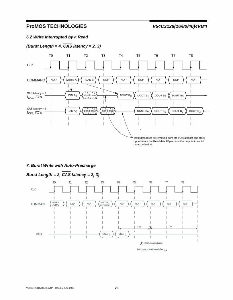
6.2 Write Interrupted by Read
7. Burst Write & Read with Auto-Precharge
7.1 Burst Write with Auto-Precharge
7.2 Burst Read with Auto-Precharge
8. Burst Termination
8.1 Termination of a Burst Write Operation
8.2 Termination of a Burst Write Operation
9. AC- Parameters
9.1 AC Parameters for a Write Timing
9.2 AC Parameters for a Read Timing
10. Mode Register Set
11. Power on Sequence and Auto Refresh (CBR)
12. Power Down Mode
13. Self Refresh (Entry and Exit)
14. Auto Refresh (CBR)
20V54C3128(16/80/40)4VB*I Rev.1.5 June 2008

ProMOS TECHNOLOGIES V54C3128(16/80/40)4VB*I
Timing Diagrams (Cont’d)
15. Random Column Read ( Page within same Bank)
15.1 CAS Latency = 2
15.2 CAS Latency = 3
16. Random Column Write ( Page within same Bank)
16.1 CAS Latency = 2
16.2 CAS Latency = 3
17. Random Row Read ( Interleaving Banks) with Precharge
17.1 CAS Latency = 2
17.2 CAS Latency = 3
18. Random Row Write ( Interleaving Banks) with Precharge
18.1 CAS Latency = 2
18.2 CAS Latency = 3
19. Precharge Termination of a Burst
19.1 CAS Latency = 2
19.2 CAS Latency = 3
20. Full Page Burst Operation
20.1 Full Page Burst Read, CAS Latency = 2
20.2 Full Page Burst Read, CAS Latency = 3
21. Full Page Burst Operation
21.1 Full Page Burst Write, CAS Latency = 2
21.2 Full Page Burst Write, CAS Latency = 3
21V54C3128(16/80/40)4VB*I Rev. 1.5 June 2008

ProMOS TECHNOLOGIES V54C3128(16/80/40)4VB*I
1. Bank Activate Command Cycle
(CAS latency = 3)
2. Burst Read Operation
(Burst Length = 4, CAS latency = 2, 3)
ADDRESS
CLK
T0 TT1 T T T T
COMMAND NOP NOP NOP
Bank ARow Addr.
Bank AActivate
Write Awith Auto
Bank ACol. Addr.
. . . . . . . . . .
. . . . . . . . . .
. . . . . . . . . . Bank BActivate
Bank ARow Addr.
Bank AActivate
tRCD
: “H” or “L”tRC
Precharge
tRRD
Bank BRow Addr.
COMMAND READ A NOP NOP NOP NOP NOP NOP NOP
DOUT A0CAS latency = 2
tCK3, I/O’sCAS latency = 3
DOUT A1 DOUT A2 DOUT A3
NOP
CLK
T0 T2T1 T3 T4 T5 T6 T7 T8
tCK2, I/O’s
DOUT A0 DOUT A1 DOUT A2 DOUT A3
22V54C3128(16/80/40)4VB*I Rev.1.5 June 2008

ProMOS TECHNOLOGIES V54C3128(16/80/40)4VB*I
3. Read Interrupted by a Read
(Burst Length = 4, CAS latency = 2, 3)
4.1 Read to Write Interval
(Burst Length = 4, CAS latency = 3)
COMMAND READ A READ B NOP NOP NOP NOP NOP NOP
tCK2, I/O’sCAS latency = 2
tCK3, I/O’sCAS latency = 3
NOP
CLK
T0 T2T1 T3 T4 T5 T6 T7 T8
DOUT B0 DOUT B1 DOUT B2 DOUT B3DOUT A0
DOUT B0 DOUT B1 DOUT B2 DOUT B3DOUT A0
tCCD
COMMAND NOP READ A NOP NOP NOP NOP WRITE B NOP NOP
DQM
DOUT A0 DIN B0 DIN B1 DIN B2
Must be Hi-Z beforethe Write Command
I/O’s
Minimum delay between the Read and Write Commands = 4+1 = 5 cycles
CLK
T0 T2T1 T3 T4 T5 T6 T7 T8
tDQZ
tDQW
: “H” or “L”
23V54C3128(16/80/40)4VB*I Rev. 1.5 June 2008

ProMOS TECHNOLOGIES V54C3128(16/80/40)4VB*I
4.2 Minimum Read to Write Interval
(Burst Length = 4, CAS latency = 2)
4.3 Non-Minimum Read to Write Interval
(Burst Length = 4, CAS latency = 2, 3)
COMMAND NOP BANK A NOP READ A WRITE A NOP NOP NOP
DQM
DIN A0 DIN A1 DIN A2 DIN A3
Must be Hi-Z beforethe Write Command
tCK2, I/O’sCAS latency = 2
CLK
T0 T2T1 T3 T4 T5 T6 T7 T8
NOPACTIVATE
1 Clk Interval
tDQZ
tDQW
: “H” or “L”
NOP READ A NOP NOP READ A NOP WRITE B NOP NOP
DQM
DIN B0 DIN B1 DIN B2
tCK1, I/O’sCAS latency = 2
tCK2, I/O’sCAS latency = 3
CLK
T0 T2T1 T3 T4 T5 T6 T7 T8
DOUT A0
COMMAND
DIN B0 DIN B1 DIN B2DOUT A1DOUT A0
Must be Hi-Z beforethe Write Command
tDQZ
tDQW
: “H” or “L”
24V54C3128(16/80/40)4VB*I Rev.1.5 June 2008

ProMOS TECHNOLOGIES V54C3128(16/80/40)4VB*I
5. Burst Write Operation
(Burst Length = 4, CAS latency = 2, 3)
6.1 Write Interrupted by a Write
(Burst Length = 4, CAS latency = 2, 3)
COMMAND NOP WRITE A NOP NOP NOP NOP NOP NOP
I/O’s DIN A0 DIN A1 DIN A2 DIN A3
NOP
CLK
T0 T2T1 T3 T4 T5 T6 T7 T8
Extra data is ignored after The first data element and the Writeare registered on the same clock edge. termination of a Burst.
don’t care
COMMAND NOP WRITE A WRITE B NOP NOP NOP NOP NOP
I/O’s DIN A0 DIN B0 DIN B1 DIN B2
NOP
DIN B3
CLK
T0 T2T1 T3 T4 T5 T6 T7 T8
1 Clk Interval
tCCD
25V54C3128(16/80/40)4VB*I Rev. 1.5 June 2008
ProMOS TECHNOLOGIES V54C3128(16/80/40)4VB*I
6.2 Write Interrupted by a Read
(Burst Length = 4, CAS latency = 2, 3)
7. Burst Write with Auto-Precharge
Burst Length = 2, CAS latency = 2, 3)
COMMAND NOP WRITE A READ B NOP NOP NOP NOP NOP NOP
tCK2, I/O’sCAS latency = 2
DIN A0
tCK3, I/O’sCAS latency = 3
DIN A0
CLK
T0 T2T1 T3 T4 T5 T6 T7 T8
DOUT B3
DOUT B0 DOUT B1 DOUT B2 DOUT B3don’t care don’t care
don’t care DOUT B0 DOUT B1 DOUT B2
Input data must be removed from the I/O’s at least one clockcycle before the Read dataAPpears on the outputs to avoiddata contention.
Burs t Lengt h = 2, CAS latency = 2, 3)
COMMAND NOP NOP NOPWRITE AAuto-Precharge
CLK
T0 T2T1 T3 T4 T5 T6 T7 T8
NOPBANK AACTIVE NOPNOP
DIN A 0 DIN A 1I/O’s
Begin Autoprecharge
Bank can be reactivated after t *
t WR tRP
NOP
*
RP
26V54C3128(16/80/40)4VB*I Rev.1.5 June 2008
ProMOS TECHNOLOGIES V54C3128(16/80/40)4VB*I
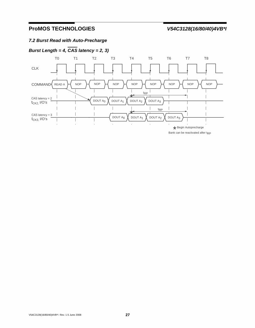
7.2 Burst Read with Auto-Precharge
Burst Length = 4, CAS latency = 2, 3)
COMMAND READ A NOP NOP NOP NOP NOP NOP
tCK2, I/O’sCAS latency = 2
tCK3, I/O’sCAS latency = 3
CLK
T0 T2T1 T3 T4 T5 T6 T7 T8
DOUT A3DOUT A
tRP
tRP
*
*
*
0 DOUT A1 DOUT A2
DOUT A3DOUT A
Begin Autoprecharge
Bank can be reactivated after tRP
0 DOUT A1 DOUT A2
NOPNOP
27V54C3128(16/80/40)4VB*I Rev. 1.5 June 2008

ProMOS TECHNOLOGIES V54C3128(16/80/40)4VB*I
8.1 Termination of a Burst Read Operation
(CAS latency = 2, 3)
8.2 Termination of a Burst Write Operation
(CAS latency = 2, 3)
COMMAND READ A NOP NOP NOP Burst NOP NOP NOP NOP
tCK2, I/O’sCAS latency = 2
tCK3, I/O’sCAS latency = 3
Stop
CLK
T0 T2T1 T3 T4 T5 T6 T7 T8
DOUT A0 DOUT A1 DOUT A2 DOUT A3
DOUT A0 DOUT A1 DOUT A2 DOUT A3
COMMAND NOP WRITE A NOP NOP Burst NOP NOP NOP NOP
DIN A0 DIN A1 DIN A2
Stop
CLK
T0 T2T1 T3 T4 T5 T6 T7 T8
Input data for the Write is masked.
I/O’sCAS latency = 2,3
don’t care
28V54C3128(16/80/40)4VB*I Rev.1.5 June 2008

ProMOS TECHNOLOGIES V54C3128(16/80/40)4VB*I
CLK
CK
E
CS
I/ORA
S
CA
S
WE
BS
DQ
M
9.1
AC
Par
amet
ers
for W
rite
Tim
ing
T2T3
T4T0
T1T6
T7T8
T9T5
T11
T12
T13
T14
T10
T16
T17
T18
T19
T15
T22
T20
T21
Hi-Z
AP
Bur
st L
engt
h =
4, C
AS
Lat
ency
= 2
A
ddr
t CKS
t ISt IH
t IS
t RC
D
t RC
t RP
t DS
Act
ivat
eC
omm
and
Ban
k A
Writ
e w
ithA
uto
Pre
char
geC
omm
and
Ban
k A
Act
ivat
eC
omm
and
Bank
B
Writ
e w
ithA
uto
Pre
char
geC
omm
and
Ban
k B
Act
ivat
eC
omm
and
Ban
k A
Writ
eC
omm
and
Ban
k A
Pre
char
geC
omm
and
Ban
k A
Act
ivat
eC
omm
and
Ban
k A
t DH
Ax0
Ax3
Ax2
Ax1
Bx0
Bx3
Bx2
Bx1
Ay0
Ay3
Ay2
Ay1
t CK2
t CHt C
L
Beg
in A
uto
Prec
harg
eB
ank
AB
egin
Aut
o P
rech
arge
Ban
k B
t RR
D
Act
ivat
eC
omm
and
Ban
k B
RA
y
CB
xR
AyR
Ay
RB
x
RB
xC
Ax
RB
y
RBy
RA
z
RAz
RA
x
RA
x
t IH
t DPL
t CKH
t IS t IH
29V54C3128(16/80/40)4VB*I Rev. 1.5 June 2008

ProMOS TECHNOLOGIES V54C3128(16/80/40)4VB*I
\
CLK
CK
E
CS
I/ORA
S
CA
S
WE
BS
DQ
M
9.2
AC
Par
amet
ers
for R
ead
Tim
ing
T2T3
T4T
0T1
T6T7
T8T9
T5T1
1T1
2T1
3T1
0
Hi-Z
AP
Bur
st L
engt
h =
2, C
AS
Lat
ency
= 2
A
ddr
t ISt IH
t CKH
t IS
t IH
t RR
D
t RCD
t RAS
t LZ
Activ
ate
Com
man
dB
ank
A
Act
ivat
eC
omm
and
Ban
k B
Act
ivat
eC
omm
and
Ban
k A
Pre
char
geC
omm
and
Ban
k A
t CK
S
t CK2
Ax0
Ax1
Rea
dC
omm
and
Bank
A
Rea
d w
ithAu
to P
rech
arge
Com
man
dB
ank
B
t RC
t RP
t AC2
t AC2
t OH
t HZ
t CHt CL
Bx0
Beg
in A
uto
Pre
char
geB
ank
B
Bx1t H
Z
RB
xR
Ay
RB
x
RB
x
RA
y
CA
xR
Ax
RA
x
30V54C3128(16/80/40)4VB*I Rev.1.5 June 2008
ProMOS TECHNOLOGIES V54C3128(16/80/40)4VB*I
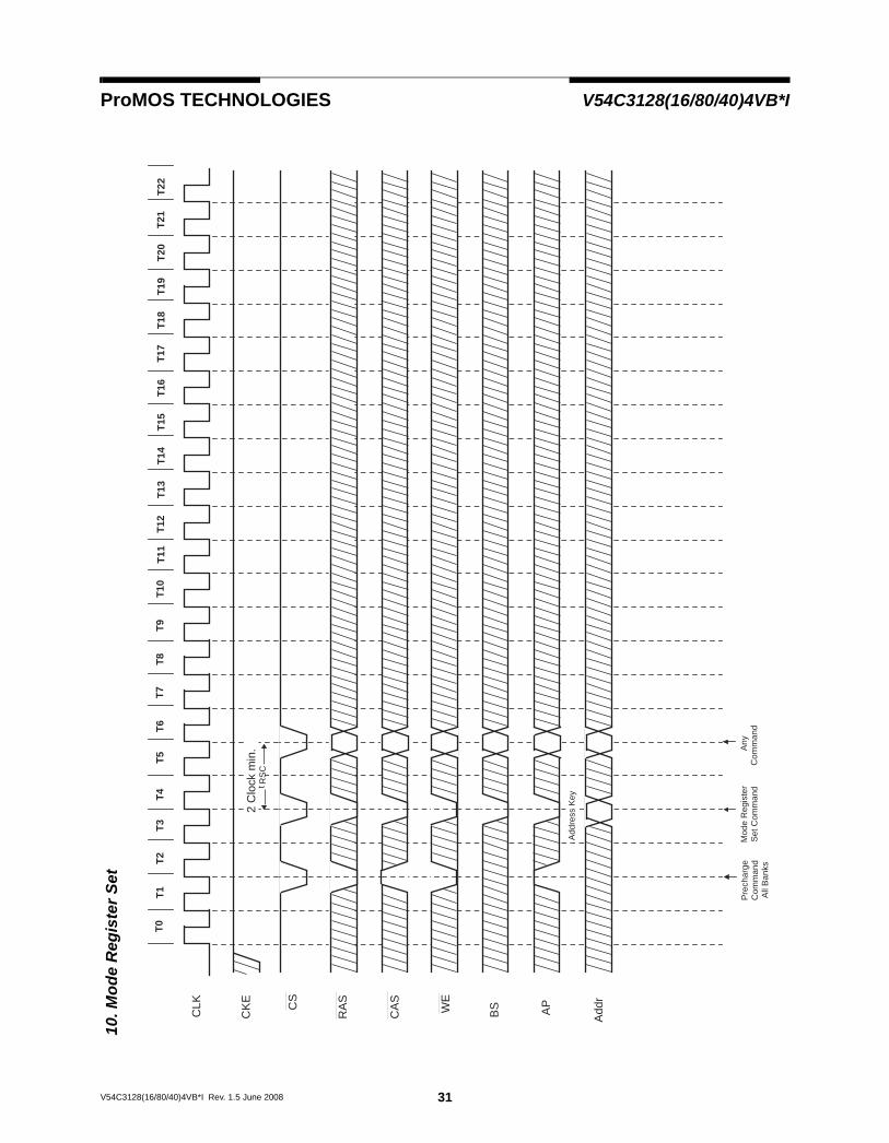
\
10. M
ode
Reg
iste
r Set
CLK
CK
E CS
RA
S
CA
S
WE
B
S
T2T3
T4T0
T1T6
T7T8
T9T5
T11
T12
T13
T14
T10
T16
T17
T18
T19
T15
T22
T20
T21
AP
A
ddr
Pre
char
geC
omm
and
All
Ban
ks
Mod
e R
egis
ter
Set
Com
man
dA
nyC
omm
and
Add
ress
Key
2 C
lock
min
.R
SC
t
31V54C3128(16/80/40)4VB*I Rev. 1.5 June 2008

ProMOS TECHNOLOGIES V54C3128(16/80/40)4VB*I
\
11. P
ower
on
Sequ
ence
and
Aut
o R
efre
sh (C
BR
)
CLK
CKE CS I/ORAS
CAS WE
BS DQ
M
Hi-Z
AP
A
ddr
Pre
char
geC
omm
and
All
Ban
ks
t RP
Min
imum
of 2
Ref
resh
Cyc
les
are
requ
ired
1st A
uto
Ref
resh
Com
man
d
t RC
Hig
h le
vel
is re
quire
d
2nd
Aut
o R
efre
shC
omm
and
Inpu
ts m
ust b
e st
able
for 2
00µ s
Any
Com
man
d
2 C
lock
min
.
Mod
e R
egis
ter
Add
ress
Key
Set
Com
man
d
T2T3
T4T0
T1T6
T7T8
T9T5
T11
T12
T13
T14
T10
T16
T17
T18
T19
T15
T22
T20
T21
32V54C3128(16/80/40)4VB*I Rev.1.5 June 2008
ProMOS TECHNOLOGIES V54C3128(16/80/40)4VB*I
\
CLK
CKE CS I/ORAS
CAS WE
BS DQM
T2T3
T4T0
T1T6
T7T8
T9T5
T11
T12
T13
T14
T10
T16
T17
T18
T19
T15
T22
T20
T21
Hi-Z
AP
A
ddr
t CKS
RAx
RAx
Activ
ate
Com
mand
Bank
A
Prec
harg
eCo
mma
ndBa
nk A
Powe
r Dow
nM
ode
Entry
Powe
r Dow
nM
ode
Exit
Any
Com
mand
t SB
12. P
ower
Dow
n M
ode
Bur
st L
engt
h =
4, C
AS
Lat
ency
= 2
33V54C3128(16/80/40)4VB*I Rev. 1.5 June 2008

ProMOS TECHNOLOGIES V54C3128(16/80/40)4VB*I
13. Sel
f Ref
resh
(Ent
ry a
nd E
xit)
BS
Add
r
AP
t
CLK
CK
E
CS
I/ORA
S
CA
S
WE
DQ
M
Hi-Z All
Ban
ksm
ust b
e id
leS
elf R
efre
shE
ntry
Beg
in S
elf R
efre
shE
xit C
omm
and
t SR
EX
Sel
f Ref
resh
Exi
tC
omm
and
issu
edS
elf R
efre
shE
xit
t RC
CK
S
34V54C3128(16/80/40)4VB*I Rev.1.5 June 2008

ProMOS TECHNOLOGIES V54C3128(16/80/40)4VB*I
\
14. A
uto
Ref
resh
(CB
R)
Bur
st L
engt
h =
4, C
AS
Lat
ency
= 2
CLK
CK
E
CS
I/ORA
S
CA
S
WE
BS
DQ
M
Hi-Z
AP
A
ddr
Ax0
Ax1
Act
ivat
eC
omm
and
Rea
dC
omm
and
Pre
char
geC
omm
and
Aut
o R
efre
shC
omm
and
Aut
o R
efre
shC
omm
and
t RC
t RP
t RC
t CK
2
All
Ban
ks
CA
xR
Ax
RA
x
Ban
k A
Ban
k A
Ax2
Ax3
(Min
imum
Inte
rval
)
T2T3
T4T0
T1T6
T7T8
T9T5
T11
T12
T13
T14
T10
T16
T17
T18
T19
T15
T22
T20
T21
35V54C3128(16/80/40)4VB*I Rev. 1.5 June 2008

ProMOS TECHNOLOGIES V54C3128(16/80/40)4VB*I
\)
15.1
Ran
dom
Col
umn
Rea
d (P
age
with
in s
ame
Ban
k) (1
of 2
)B
urst
Len
gth
= 4,
CAS
Lat
ency
= 2
CLK
CK
E
CS
I/ORA
S
CA
S
WE
BS
DQ
M
Hi-Z
AP
A
ddr
Act
ivat
eC
omm
and
Ban
k A
CA
x
Rea
dC
omm
and
Ban
k A
CA
y
Rea
dC
omm
and
Ban
k A
Aw
0A
w1
Aw
2A
w3
Ax0
Ax1
Ay0
Ay1
Az0
Az1
Az2
Az3
Ay2
Ay3
CA
w
Rea
dC
omm
and
Ban
k A
RA
w
RA
w
Pre
char
geC
omm
and
Ban
k A
Act
ivat
eC
omm
and
Ban
k A
CA
z
Rea
dC
omm
and
Ban
k A
RA
z
RA
z
t CK
2
T2T3
T4T0
T1T6
T7T8
T9T5
T11
T12
T13
T14
T10
T16
T17
T18
T19
T15
T22
T20
T21
36V54C3128(16/80/40)4VB*I Rev.1.5 June 2008
ProMOS TECHNOLOGIES V54C3128(16/80/40)4VB*I
\)
15.2
Ran
dom
Col
umn
Rea
d (P
age
with
in s
ame
Ban
k) (2
of 2
)B
urst
Len
gth
= 4,
CA
S La
tenc
y =
3
CLK
CK
E
CS
I/ORA
S
CA
S
WE
B
S
DQ
M
T2T3
T4T0
T1T6
T7T8
T9T5
T11
T12
T13
T14
T10
T16
T17
T18
T19
T15
T22
T20
T21
Hi-Z
AP
A
ddr
Act
ivat
eC
omm
and
Ban
k A
CA
x
Rea
dC
omm
and
Ban
k A
CA
y
Rea
dC
omm
and
Ban
k A
Aw
0A
w1
Aw
2A
w3
Ax0
Ax1
Ay0
Ay1
Ay2
Ay3
CA
w
Rea
dC
omm
and
Ban
k A
RA
w
RA
w
Pre
char
geC
omm
and
Ban
k A
Act
ivat
eC
omm
and
Ban
k A
CA
z
Rea
dC
omm
and
Ban
k A
RA
z
RA
z
t CK
3
37V54C3128(16/80/40)4VB*I Rev. 1.5 June 2008
ProMOS TECHNOLOGIES V54C3128(16/80/40)4VB*I
\)16.1
Ran
dom
Col
umn
Writ
e (P
age
with
in s
ame
Ban
k) (1
of 2
)B
urst
Len
gth
= 4,
CA
S L
aten
cy =
2
CLK
CK
E
CS
I/ORA
S
CA
S
WE
BS
DQ
M
T2T3
T4T0
T1T6
T7T8
T9T5
T11
T12
T13
T14
T10
T16
T17
T18
T19
T15
T22
T20
T21
Hi-Z
AP
A
ddr
CB
x
Writ
eC
omm
and
Ban
k B
CB
y
Writ
eC
omm
and
Ban
k B
Pre
char
geC
omm
and
Ban
k B
DB
w0
DB
w3
DB
w2
DB
w1
DB
x1D
Bx0
DB
y0D
By3
DB
y2D
By1
DB
z0D
Bz3
DB
z2D
Bz1
t CK
2
Act
ivat
eC
omm
and
Ban
k B
CA
x
Writ
eC
omm
and
Ban
k B
RA
w
RA
w
Act
ivat
eC
omm
and
Ban
k B
CB
z
Writ
eC
omm
and
Ban
k B
RB
z
RB
z
Act
ivat
eC
omm
and
Ban
k B
CB
z
Writ
eC
omm
and
Ban
k B
RB
z
RB
z
38V54C3128(16/80/40)4VB*I Rev.1.5 June 2008
ProMOS TECHNOLOGIES V54C3128(16/80/40)4VB*I
\)
16.2
Ran
dom
Col
umn
Writ
e (P
age
with
in s
ame
Ban
k) (2
of 2
)B
urst
Len
gth
= 4,
CA
S L
aten
cy =
3
CLK
CK
E
CS
I/ORA
S
CA
S
WE
BS
DQ
M
T2T3
T4T0
T1T6
T7T8
T9T5
T11
T12
T13
T14
T10
T16
T17
T18
T19
T15
T22
T20
T21
Hi-Z
AP
A
ddr
CB
x
Writ
eC
omm
and
Ban
k B
CB
y
Writ
eC
omm
and
Ban
k B
Pre
char
geC
omm
and
Ban
k B
DB
w0
DB
w3
DB
w2
DB
w1
DB
x1D
Bx0
DB
y0D
By3
DB
y2D
By1
DB
z0D
Bz1
t CK
3
Act
ivat
eC
omm
and
Ban
k B
CB
z
Writ
eC
omm
and
Ban
k B
RB
z
RB
z
Act
ivat
eC
omm
and
Ban
k B
CB
z
Writ
eC
omm
and
Ban
k B
RB
z
RB
z
39V54C3128(16/80/40)4VB*I Rev. 1.5 June 2008
40V54C3128(16/80/40)4VB*I Rev.1.5 June 2008
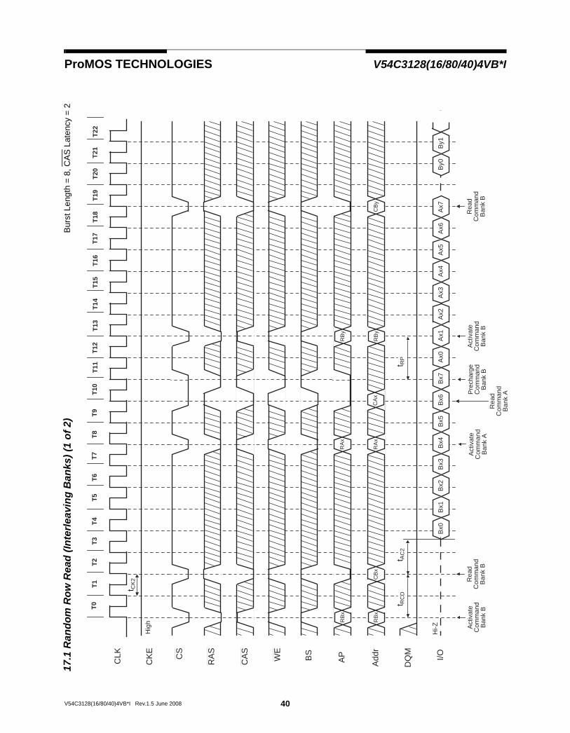
ProMOS TECHNOLOGIES V54C3128(16/80/40)4VB*I17
.1 R
ando
m R
ow R
ead
(Inte
rleav
ing
Ban
ks) (
1 of
2)
Bur
st L
engt
h =
8, C
AS
Lat
ency
= 2
CLK
CK
E
CS
I/ORA
S
CA
S
WE
BS
DQ
M
T2T3
T4T0
T1T6
T7T8
T9T5
T11
T12
T13
T14
T10
T16
T17
T18
T19
T15
T22
T20
T21
Hi-Z
AP
A
ddr
CB
y
Rea
dC
omm
and
Ban
k B
Rea
dC
omm
and
Ban
k A
Bx0
Bx1
Bx2
Bx3
Bx4
Bx5
Bx6
Bx7
By0
By1
t CK
2
Hig
h
t RC
Dt A
C2
t RP
CA
x
Pre
char
geC
omm
and
Ban
k B
Ax0
Ax1
Ax2
Ax3
Ax4
Ax5
Ax6
Ax7
Act
ivat
eC
omm
and
Ban
k B
RB
x
RB
x
Act
ivat
eC
omm
and
Ban
k A
RA
x
RA
x
CB
x
Rea
dC
omm
and
Ban
k B
Act
ivat
eC
omm
and
Ban
k B
RB
y
RB
y

41V54C3128(16/80/40)4VB*I Rev. 1.5 June 2008
ProMOS TECHNOLOGIES V54C3128(16/80/40)4VB*I17
. 2 R
ando
m R
ow R
ead
(Inte
rleav
ing
Ban
ks) (
2 of
2)
Bur
st L
engt
h =
8, C
AS
Lat
ency
= 3
CLK
CK
E
CS
I/ORA
S
CA
S
WE
BS
DQ
M
T2T3
T4T0
T1T6
T7T8
T9T5
T11
T12
T13
T14
T10
T16
T17
T18
T19
T15
T22
T20
T21
Hi-Z
AP
A
ddr
CB
y
Rea
dC
omm
and
Ban
k B
By0
t CK
3
Hig
h
t AC
3
Act
ivat
eC
omm
and
Ban
k B
RB
x
RB
x
Act
ivat
eC
omm
and
Ban
k A
RA
x
RA
x
CB
x
Rea
dC
omm
and
Ban
k B
Act
ivat
eC
omm
and
Ban
k B
RB
y
RB
y
t RC
D
Pre
char
geC
omm
and
Ban
k B
CA
x
Rea
dC
omm
and
Ban
k A
t RP
Bx0
Bx1
Bx2
Bx3
Bx4
Bx5
Bx6
Bx7
Ax0
Ax1
Ax2
Ax3
Ax4
Ax5
Ax6
Ax7
Pre
char
geC
omm
and
Ban
k A

42V54C3128(16/80/40)4VB*I Rev.1.5 June 2008
ProMOS TECHNOLOGIES V54C3128(16/80/40)4VB*I18
.1 R
ando
m R
ow W
rite
(Inte
rleav
ing
Ban
ks) (
1 of
2)
Bur
st L
engt
h =
8, C
AS
Lat
ency
= 2
CLK
CK
E
CS
I/ORA
S
CA
S
WE
BS
DQ
M
T2T3
T4T0
T1T6
T7T8
T9T5
T11
T12
T13
T14
T10
T16
T17
T18
T19
T15
T22
T20
T21
Hi-Z
AP
A
ddr
t CK
2
Hig
h
t RC
Dt R
P
Writ
eC
omm
and
Ban
k A
CA
y
DA
x0D
Ax3
DA
x2D
Ax1
DA
x4D
Ax7
DA
x6D
Ax5
DB
x0D
Bx3
DB
x2D
Bx1
DB
x4D
Bx7
DB
x6D
Bx5
DA
y0D
Ay3
DA
y2D
Ay1
t DP
L
Writ
eC
omm
and
Ban
k A
CA
X
Act
ivat
eC
omm
and
Ban
k A
RA
x
RA
x
Act
ivat
eC
omm
and
Ban
k B
RB
x
RB
xC
Bx
Pre
char
geC
omm
and
Ban
k A
Writ
eC
omm
and
Ban
k B
Act
ivat
eC
omm
and
Ban
k A
RA
y
RA
y
CA
y
Pre
char
geC
omm
and
Ban
k B
Writ
eC
omm
and
Ban
k A
DA
y4
t DP
L

43V54C3128(16/80/40)4VB*I Rev. 1.5 June 2008
ProMOS TECHNOLOGIES V54C3128(16/80/40)4VB*I18
.2 R
ando
m R
ow W
rite
(Inte
rleav
ing
Ban
ks) (
2 of
2)
Bur
st L
engt
h =
8, C
AS
Lat
ency
= 3
CLK
CK
E
CS
I/ORA
S
CA
S
WE
BS
DQ
M
T2T3
T4T0
T1T6
T7T8
T9T5
T11
T12
T13
T14
T10
T16
T17
T18
T19
T15
T22
T20
T21
Hi-Z
AP
A
ddr
t CK
3
Hig
h
DA
x0D
Ax3
DA
x2D
Ax1
DA
x4D
Ax7
DA
x6D
Ax5
DB
x0D
Bx3
DB
x2D
Bx1
DB
x4D
Bx7
DB
x6D
Bx5
DA
y2D
Ay1
DA
y0
Writ
eC
omm
and
Ban
k A
CA
X
Act
ivat
eC
omm
and
Ban
k B
RB
x
RB
x
Act
ivat
eC
omm
and
Ban
k A
RA
y
RA
y
DA
y3
t DP
L
CB
x
Writ
eC
omm
and
Ban
k B
Pre
char
geC
omm
and
Ban
k A
Writ
eC
omm
and
Ban
k A
CA
y
Pre
char
geC
omm
and
Ban
k B
t RP
t DP
Lt R
CD
Act
ivat
eC
omm
and
Ban
k A
RA
x
RA
x
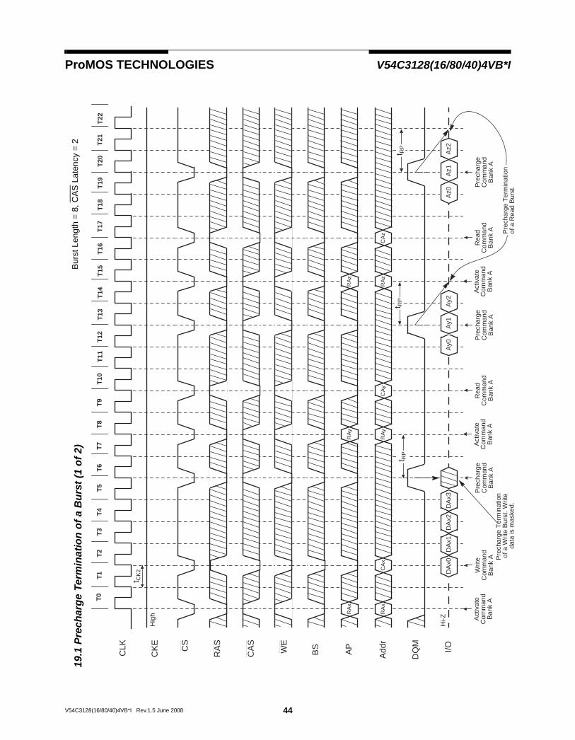
ProMOS TECHNOLOGIES V54C3128(16/80/40)4VB*I
19.1 P
rech
arge
Ter
min
atio
n of
a B
urst
(1 o
f 2)
Bur
st L
engt
h =
8, C
AS
Lat
ency
= 2
CLK
CK
E
CS
I/ORA
S
CA
S
WE
BS
DQ
M
T2T3
T4T0
T1T6
T7T8
T9T5
T11
T12
T13
T14
T10
T16
T17
T18
T19
T15
T22
T20
T21
Hi-Z
AP
A
ddr
t CK
2
Pre
char
geC
omm
and
Ban
k A
DA
x0D
Ax3
DA
x2D
Ax1
Pre
char
ge T
erm
inat
ion
of a
Writ
e B
urst
. Writ
eda
ta is
mas
ked.
Ay0
Ay1
Ay2
Pre
char
ge T
erm
inat
ion
of a
Rea
d B
urst
.
Pre
char
geC
omm
and
Ban
k A
t RP
Act
ivat
eC
omm
and
Ban
k A
RA
x
RA
x
Writ
eC
omm
and
Ban
k A
CA
xC
Ay
Rea
dC
omm
and
Ban
k A
Hig
h
Act
ivat
eC
omm
and
Ban
k A
RA
y
RA
y
t RP
Act
ivat
eC
omm
and
Ban
k A
RA
z
RA
z
CA
z
Rea
dC
omm
and
Ban
k A
Az0
Az1
Az2
Pre
char
geC
omm
and
Ban
k A
t RP
44V54C3128(16/80/40)4VB*I Rev.1.5 June 2008
ProMOS TECHNOLOGIES V54C3128(16/80/40)4VB*I
19.2 P
rech
arge
Ter
min
atio
n of
a B
urst
(2 o
f 2)
Bur
st L
engt
h =
4, 8
, CA
S L
aten
cy =
3
CLK
CK
E
CS
I/ORA
S
CA
S
WE
B
S
DQ
M
T2T3
T4T0
T1T6
T7T8
T9T5
T11
T12
T13
T14
T10
T16
T17
T18
T19
T15
T22
T20
T21
Hi-Z
AP
A
ddr
t CK
3
Pre
char
geC
omm
and
Ban
k A
DA
x0
Pre
char
ge T
erm
inat
ion
of a
Writ
e B
urst
.W
rite
Dat
a is
mas
ked
Ay0
Ay1
Ay2
Pre
char
ge T
erm
inat
ion
Pre
char
geC
omm
and
Ban
k A
t RP
Act
ivat
eC
omm
and
Ban
k A
RA
x
RA
x
Writ
eC
omm
and
Ban
k A
CA
xC
Ay
Rea
dC
omm
and
Ban
k A
Hig
h
Act
ivat
eC
omm
and
Ban
k A
RA
y
RA
y
t RP
Act
ivat
eC
omm
and
Ban
k A
RA
z
RA
z
of a
Rea
d B
urst
.
45V54C3128(16/80/40)4VB*I Rev. 1.5 June 2008
46V54C3128(16/80/40)4VB*I Rev.1.5 June 2008
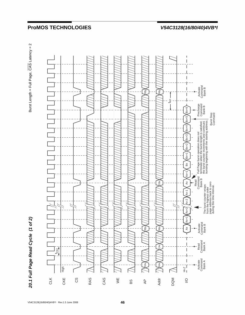
ProMOS TECHNOLOGIES V54C3128(16/80/40)4VB*I20
.1 F
ull P
age
Rea
d C
ycle
(1
of 2
)B
urst
Len
gth
= Fu
ll P
age,
CA
S L
aten
cy =
2
CLK
CK
E
CS
I/ORA
S
CA
S
WE
BS
DQ
M
Hi-Z
AP
A
ddr
t CK
2
Hig
h
Ax
Ax+
1A
x-1
Ax-
2A
x+2
Ax
Bx
Bx+
1B
x+5
Bx+
4B
x+3
Bx+
2A
x+1
Bx+
6
CB
x
Rea
dC
omm
and
Ban
k B
Pre
char
geC
omm
and
Ban
k B
Bur
st S
top
Com
man
d
CA
x
Rea
dC
omm
and
Ban
k A
Act
ivat
eC
omm
and
Ban
k A
RA
x
RA
x
Act
ivat
eC
omm
and
Ban
k B
RB
x
RB
x
Act
ivat
eC
omm
and
Ban
k B
RB
y
RB
y
t RP
Ful
l Pag
e bu
rst o
pera
tion
does
not
term
inat
e w
hen
the
burs
t len
gth
is s
atis
fied;
the
burs
t cou
nter
incr
emen
ts a
nd c
ontin
ues
The
bur
st c
ount
er w
raps
from
the
high
est o
rder
page
add
ress
bac
k to
zer
odu
ring
this
tim
e in
terv
al.
burs
ting
begi
nnin
g w
ith th
e st
artin
g ad
dres
s.

47V54C3128(16/80/40)4VB*I Rev. 1.5 June 2008
ProMOS TECHNOLOGIES V54C3128(16/80/40)4VB*I
\
20.2
Ful
l Pag
e R
ead
Cyc
le (
2 of
2)
Bur
st L
engt
h =
Full
Pag
e, C
AS
Lat
ency
= 3
CLK
CK
E
CS
I/ORA
S
CA
S
WE
BS
DQ
M
Hi-Z
AP
A
ddr
t CK
3
Hig
h
Ax
Ax+
1A
x-1
Ax-
2A
x+2
Ax
Bx
Bx+
1B
x+5
Bx+
4B
x+3
Bx+
2A
x+1
CB
x
Rea
dC
omm
and
Ban
k B
Pre
char
geC
omm
and
Ban
k B
Bur
st S
top
Com
man
d
CA
x
Rea
dC
omm
and
Ban
k A
Act
ivat
eC
omm
and
Ban
k A
RA
x
RA
x
Act
ivat
eC
omm
and
Ban
k B
RB
x
RB
x
Act
ivat
eC
omm
and
Ban
k B
RB
y
RB
y
t RR
D
Ful
l Pag
e bu
rst o
pera
tion
does
not
The
bur
st c
ount
er w
raps
from
the
high
est o
rder
page
add
ress
bac
k to
zer
odu
ring
this
tim
e in
terv
al.
term
inat
e w
hen
the
leng
th is
satis
fied;
the
burs
t cou
nter
incr
emen
ts a
nd c
ontin
ues
burs
ting
begi
nnin
g w
ith
the
star
ting
addr
ess.
48V54C3128(16/80/40)4VB*I Rev.1.5 June 2008
ProMOS TECHNOLOGIES V54C3128(16/80/40)4VB*I21
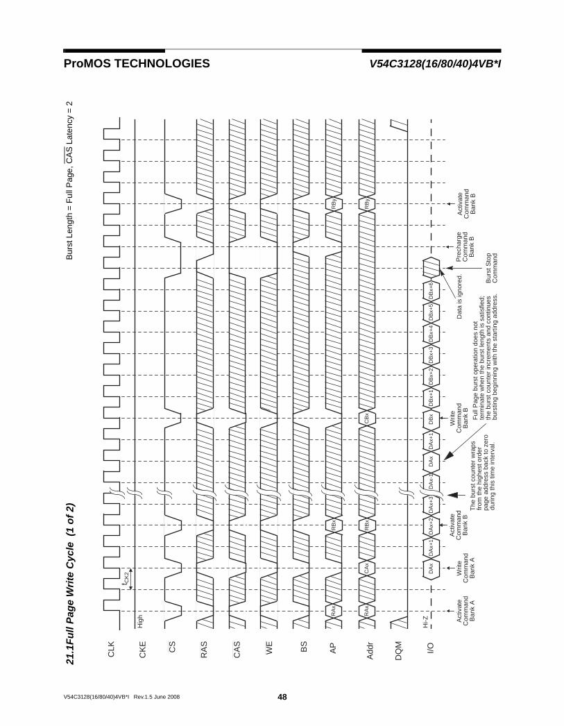
.1Fu
ll Pa
ge W
rite
Cyc
le (
1 of
2)
Bur
st L
engt
h =
Full
Pag
e, C
AS
Lat
ency
= 2
CLK
CK
E
CS
I/ORA
S
CA
S
WE
BS
DQ
M
Hi-Z
AP
A
ddr
t CK
2
Hig
h
CB
x
Writ
eC
omm
and
Ban
k B
Pre
char
geC
omm
and
Ban
k B
Bur
st S
top
Com
man
d
CA
x
Writ
eC
omm
and
Ban
k A
Act
ivat
eC
omm
and
Ban
k A
RA
x
RA
x
Act
ivat
eC
omm
and
Ban
k B
RB
x
RB
x
Act
ivat
eC
omm
and
Ban
k B
RB
y
RB
y
Dat
a is
igno
red.
DA
xD
Ax+
1D
Ax-
1D
Ax+
3D
Ax+
2D
Ax
DB
xD
Bx+
1D
Ax+
1D
Bx+
3D
Bx+
2D
Bx+
4D
Bx+
5D
Bx+
6
Ful
l Pag
e bu
rst o
pera
tion
does
not
term
inat
e w
hen
the
burs
t len
gth
is s
atis
fied;
the
burs
t cou
nter
incr
emen
ts a
nd c
ontin
ues
The
bur
st c
ount
er w
raps
from
the
high
est o
rder
page
add
ress
bac
k to
zer
odu
ring
this
tim
e in
terv
al.
burs
ting
begi
nnin
g w
ith th
e st
artin
g ad
dres
s.
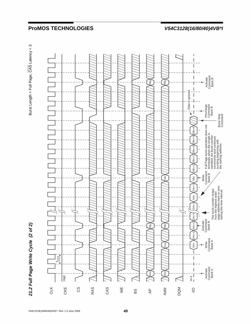
49V54C3128(16/80/40)4VB*I Rev. 1.5 June 2008
ProMOS TECHNOLOGIES V54C3128(16/80/40)4VB*I21
.2 F
ull P
age
Writ
e C
ycle
(2
of 2
)B
urst
Len
gth
= Fu
ll Pa
ge, C
AS
Late
ncy
= 3
CLK
CK
E
CS
I/ORA
S
CA
S
WE
BS
DQ
M
Hi-Z
AP
A
ddr
t CK
3
Hig
h
CB
x
Writ
eC
omm
and
Ban
k B
Pre
char
geC
omm
and
Ban
k B
Bur
st S
top
Com
man
d
CA
x
Writ
eC
omm
and
Ban
k A
Act
ivat
eC
omm
and
Ban
k A
RA
x
RA
x
Act
ivat
eC
omm
and
Ban
k B
RB
x
RB
x
Act
ivat
eC
omm
and
Ban
k B
RB
y
RB
y
DA
xD
Ax+
1D
Ax-
1D
Ax+
3D
Ax+
2D
Ax
DB
xD
Bx+
1D
Ax+
1D
Bx+
3D
Bx+
2D
Bx+
4D
Bx+
5
Ful
l Pag
e bu
rst o
pera
tion
does
not
The
bur
st c
ount
er w
raps
from
the
high
est o
rder
page
add
ress
bac
k to
zer
odu
ring
this
tim
e in
terv
al.
term
inat
e w
hen
the
leng
th is
satis
fied;
the
burs
t cou
nter
incr
emen
ts a
nd c
ontin
ues
burs
ting
begi
nnin
g w
ith
the
star
ting
addr
ess.
Dat
a is
igno
red.

ProMOS TECHNOLOGIES V54C3128(16/80/40)4VB*I
Complete List of Operation Commands
SDRAM Function Truth Table
CURRENTSTATE1 CS RAS CAS WE BS Addr ACTION
Idle HLLLLLLL
XHHHLLLL
XHHLHHLL
XHLXHLHL
XXBSBSBSBSXOp-
XXXXRAAPXCode
NOP or Power DownNOP ILLEGAL2
ILLEGAL2
Row (&Bank) Active; Latch Row AddressNOP4
Auto-Refresh or Self-Refresh5
Mode reg. Access5
Row Active HLLLLLL
XHHHLLL
XHLLHHL
XXHLHLX
XXBSBSBSBSX
XXCA,APCA,APXAPX
NOPNOPBegin Read; Latch CA; DetermineAPBegin Write; Latch CA; DetermineAPILLEGAL2
PrechargeILLEGAL
Read HLLLLLLL
XHHHHLLL
XHHLLHHL
XHLHLHLX
XXBSBSBSBSBSX
XXXCA,APCA,APXAPX
NOP (Continue Burst to End;>Row Active)NOP (Continue Burst to End;>Row Active)Burst Stop Command > Row ActiveTerm Burst, New Read, DetermineAP3
Term Burst, Start Write, DetermineAP3
ILLEGAL2
Term Burst, PrechargeILLEGAL
Write HLLLLLLL
XHHHHLLL
XHHLLHHL
XHLHLHLX
XXBSBSBSBSBSX
XXXCA,APCA,APXAPX
NOP (Continue Burst to End;>Row Active)NOP (Continue Burst to End;>Row Active)Burst Stop Command > Row ActiveTerm Burst, Start Read, DetermineAP3
Term Burst, New Write, DetermineAP3
ILLEGAL2
Term Burst, Precharge3
ILLEGAL
Read withAuto Precharge
HLLLLLLL
XHHHHLLL
XHHLLHHL
XHLHLHLX
XXBSBSXBSBSX
XXXXXXAPX
NOP (Continue Burst to End;> Precharge)NOP (Continue Burst to End;> Precharge)ILLEGAL2
ILLEGAL2
ILLEGALILLEGAL2
ILLEGAL2
ILLEGAL
50V54C3128(16/80/40)4VB*I Rev.1.5 June 2008
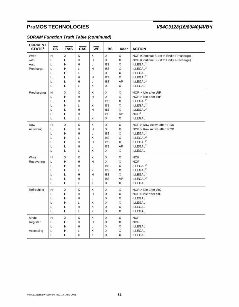
ProMOS TECHNOLOGIES V54C3128(16/80/40)4VB*I
SDRAM Function Truth Table (continued)
CURRENTSTATE1 CS RAS CAS WE BS Addr ACTION
Write withAuto Precharge
HLLLLLLL
XHHHHLLL
XHHLLHHL
XHLHLHLX
XXBSBSXBSBSX
XXXXXXAPX
NOP (Continue Burst to End;> Precharge)NOP (Continue Burst to End;> Precharge)ILLEGAL2
ILLEGAL2
ILLEGALILLEGAL2
ILLEGAL2
ILLEGAL
Precharging HLLLLLL
XHHHLLL
XHHLHHL
XHLXHLX
XXBSBSBSBSX
XXXXXAPX
NOP;> Idle after tRPNOP;> Idle after tRPILLEGAL2
ILLEGAL2
ILLEGAL2
NOP4
ILLEGAL
Row Activating
HLLLLLL
XHHHLLL
XHHLHHL
XHLXHLX
XXBSBSBSBSX
XXXXXAPX
NOP;> Row Active after tRCDNOP;> Row Active after tRCDILLEGAL2
ILLEGAL2
ILLEGAL2
ILLEGAL2
ILLEGAL
WriteRecovering
HLLLLLL
XHHHLLL
XHHLHHL
XHLXHLX
XXBSBSBSBSX
XXXXXAPX
NOPNOPILLEGAL2
ILLEGAL2
ILLEGAL2
ILLEGAL2
ILLEGAL
Refreshing HLLLLL
XHHHLL
XHHLHL
XHLXXX
XXXXXX
XXXXXX
NOP;> Idle after tRCNOP;> Idle after tRCILLEGALILLEGALILLEGALILLEGAL
Mode Register
Accessing
HLLLL
XHHHL
XHHLX
XHLXX
XXXXX
XXXXX
NOPNOPILLEGALILLEGALILLEGAL
51V54C3128(16/80/40)4VB*I Rev. 1.5 June 2008

ProMOS TECHNOLOGIES V54C3128(16/80/40)4VB*I
Clock Enable (CKE) Truth Table:
Abbreviations:
RA = Row Address of Bank A CA = Column Address of Bank A BS = Bank Address
RB = Row Address of Bank B CB = Column Address of Bank B AP = Auto Precharge
RC = Row Address of Bank C CC = Column Address of Bank C
RD = Row Address of Bank D CD = Column Address of Bank D
Notes for SDRAM function truth table:
1. Current State is state of the bank determined by BS. All entries assume that CKE was active (HIGH) during the preceding clock cycle.2. Illegal to bank in specified state; Function may be legal in the bank indicated by BS, depending on the state of that bank.3. Must satisfy bus contention, bus turn around, and/or write recovery requirements.4. NOP to bank precharging or in Idle state. May precharge bank(s) indicated by BS (andAP).5. Illegal if any bank is not Idle.6. CKE Low to High transition will re-enable CLK and other inputs asynchronously. A minimum setup time must be satisfied before any
command other than EXIT.7. Power-Down and Self-Refresh can be entered only from the All Banks Idle State.8. Must be legal command as defined in the SDRAM function truth table.
STATE(n)CKEn-1
CKEn CS RAS CAS WE Addr ACTION
Self-Refresh6
HLLLLLL
XHHHHHL
XHLLLLX
XXHHHLX
XXHHLXX
XXHLXXX
XXXXXXX
INVALIDEXIT Self-Refresh, Idle after tRCEXIT Self-Refresh, Idle after tRCILLEGALILLEGALILLEGALNOP (Maintain Self-Refresh)
Power-Down
HLLLLLL
XHHHHHL
XHLLLLX
XXHHHLX
XXHHLXX
XXHLXXX
XXXXXXX
INVALIDEXIT Power-Down, > Idle.EXIT Power-Down, > Idle.ILLEGALILLEGALILLEGALNOP (Maintain Low-Power Mode)
All. Banks Idle7
HHHHHHHHL
HLLLLLLLL
XHLLLLLLX
XXHHHLLLX
XXHHLHLLX
XXHLXXHLX
XXXXXXXXX
Refer to the function truth tableEnter Power- DownEnter Power- DownILLEGALILLEGALILLEGALEnter Self-RefreshILLEGALNOP
52V54C3128(16/80/40)4VB*I Rev.1.5 June 2008

53V54C3128(16/80/40)4VB*I Rev. 1.5 June 2008
ProMOS TECHNOLOGIES V54C3128(16/80/40)4VB*I
Package Diagram 54 Ball FBGA
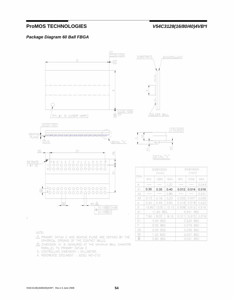
ProMOS TECHNOLOGIES V54C3128(16/80/40)4VB*I
Package Diagram 60 Ball FBGA60 PINS SOC
0.30 0.35 0.40 0.012 0.014 0.016
54V54C3128(16/80/40)4VB*I Rev.1.5 June 2008
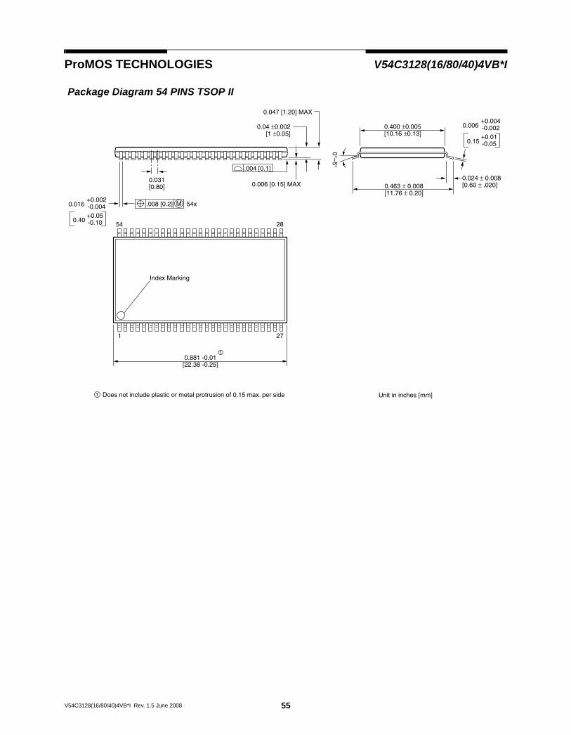
ProMOS TECHNOLOGIES V54C3128(16/80/40)4VB*I
Package Diagram 54 PINS TSOP II
0.881 -0.01[22.38 -0.25]
0.031[0.80]
.004 [0.1]
54
Index Marking
M
28
1
Does not include plastic or metal protrusion of 0.15 max. per side
1
27
0.047 [1.20] MAX
0.04 ±0.002 [1 ±0.05]
Unit in inches [mm]
0.400 ±0.005[10.16 ±0.13]
0.463 ± 0.008[11.76 ± 0.20]
0.006 [0.15] MAX
+0.004-0.002
0°–5°
0.024 ± 0.008[0.60 ± .020]
1
0.006
+0.01-0.050.15
.008 [0.2] 54x+0.002-0.0040.016
+0.05-0.100.40
55V54C3128(16/80/40)4VB*I Rev. 1.5 June 2008

56V54C3128(16/80/40)4VB*I Rev.1.5 June 2008
ProMOS TECHNOLOGIES V54C3128(16/80/40)4VB*I
WORLDWIDE OFFICES
© Copyright ,ProMOS TECHNOLOGY. Printed in U.S.A.
The information in this document is subject to change withoutnotice.
ProMOS TECH makes no commitment to update or keep cur-rent the information contained in this document. No part of thisdocument may be copied or reproduced in any form or by anymeans without the prior written consent of ProMOS TECH.
ProMOS TECH subjects its products to normal quality controlsampling techniques which are intended to provide an assuranceof high quality products suitable for usual commercial applica-tions. ProMOS TECH does not do testing appropriate to provide100% product quality assurance and does not assume any liabil-ity for consequential or incidental arising from any use of its prod-ucts. If such products are to be used in applications in whichpersonal injury might occur from failure, purchaser must do itsown quality assurance testing appropriate to such applications.
TAIWAN(Taipei)7F, NO. 102 MIN-CHUAN E. ROADSEC. 3, Taipei, Taiwan, R.O.CPHONE: 886-2-2545-1213 FAX: 886-2-2545-1209
NO. 19 LI HSIN ROADSCIENCE BASED IND. PARKHSIN CHU, TAIWAN, R.O.C.PHONE: 886-3-566-3952
FAX: 886-3-578-6028
JAPANONZE 1852 BUILDING 6F2-14-6 SHINTOMI, CHUO-KUTOKYO 104-0041PHONE: 81-3-3537-1400
FAX: 81-3-3537-1402
USA(West)3910 NORTH FIRST STREETSAN JOSE, CA 95134PHONE: 408-433-6000
FAX: 408-433-0952
SALES OFFICES:
TAIWAN(Hsinchu)
USA(East)25 Creekside RoadHopewell Jct, NY 12533PHONE:845-223-1689
FAX:845-223-1684
Related Documents