SiGe, Ge, and Related Compounds 5: Materials, Processing, and Devices D. Harame IBM, Systems and Technology Group Essex Junction, Vermont, USA T. Krishnamohan Intel Corporation Santa Clara, California, USA S. Miyazaki Nagoya University Nagoya, Japan A. Reznicek IBM, T.J. Watson Research Center Yorktown Heights, New York, USA B. Tillack IHP Frankfurt (Oder), Germany and TU Berlin Berlin, Germany Y. C. Yeo The National University of Singapore Singapore M. Caymax imec Leuven, Belgium G. Masini Luxtera Carlsbad, California, USA G. Niu Auburn University Auburn, Alabama, USA K. Saraswat Stanford University Palo Alto, California, USA B. Vincent imec Leuven, Belgium K. Uchida Keio University Yokohama, Japan Editors: Sponsoring Division: Published by The Electrochemical Society 65 South Main Street, Building D Pennington, NJ 08534-2839, USA tel 609 737 1902 fax 609 737 2743 www.electrochem.org TM Vol. 50, No. 9 Electronics and Photonics

Welcome message from author
This document is posted to help you gain knowledge. Please leave a comment to let me know what you think about it! Share it to your friends and learn new things together.
Transcript
SiGe, Ge, and Related Compounds 5: Materials, Processing, and Devices
D. HarameIBM, Systems and Technology GroupEssex Junction, Vermont, USA
T. KrishnamohanIntel CorporationSanta Clara, California, USA
S. MiyazakiNagoya UniversityNagoya, Japan
A. ReznicekIBM, T.J. Watson Research CenterYorktown Heights, New York, USA
B. TillackIHPFrankfurt (Oder), GermanyandTU BerlinBerlin, Germany
Y. C. YeoThe National University of SingaporeSingapore
M. CaymaximecLeuven, Belgium
G. MasiniLuxteraCarlsbad, California, USA
G. NiuAuburn UniversityAuburn, Alabama, USA
K. SaraswatStanford UniversityPalo Alto, California, USA
B. VincentimecLeuven, Belgium
K. UchidaKeio UniversityYokohama, Japan
Editors:
Sponsoring Division:
Published by
The Electrochemical Society65 South Main Street, Building DPennington, NJ 08534-2839, USAtel 609 737 1902fax 609 737 2743www.electrochem.org
TM
Vol. 50, No. 9
Electronics and Photonics
Copyright 2012 by The Electrochemical Society.All rights reserved.
This book has been registered with Copyright Clearance Center.For further information, please contact the Copyright Clearance Center,
Salem, Massachusetts.
Published by:
The Electrochemical Society65 South Main Street
Pennington, New Jersey 08534-2839, USA
Telephone 609.737.1902Fax 609.737.2743
e-mail: [email protected]: www.electrochem.org
ISSN 1938-6737 (online)ISSN 1938-5862 (print)
ISSN 2151-2051 (cd-rom)
ISBN 978-1-62332-008-9 (Hardcover)ISBN 978-1-60768-357-5 (PDF)
Printed in the United States of America.
iii
PREFACE
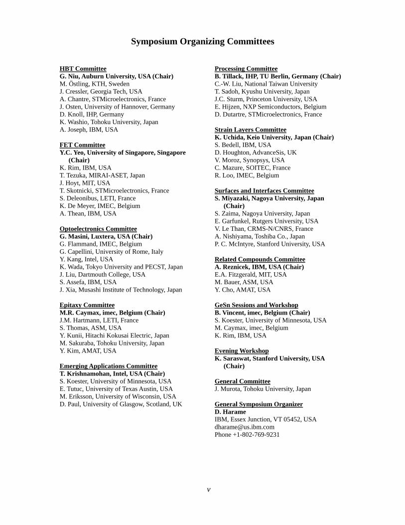
This issue of ECS Transactions (ECST) contains papers presented at the 5th SiGe, Ge, & Related Compounds: Materials, Processing and Devices Symposium held at the 220th meeting of the Electrochemical Society in Honolulu, Hawaii, October 7-12, 2012. The meeting grew out of a desire for the ECS to have a special ongoing symposium on SiGe & Ge as a materials system with increasing importance in silicon semiconductor technology. Since that time, SiGe and Ge have become a core component in CMOS and BiCMOS processes and are used in mainstream production technologies throughout the world. In 2008, the symposium was expanded to include Ge and Related compounds including SiC and III-Vs on Silicon to recognize the important emerging work in these areas. In 2010, the symposium was expanded to include work in nano-wires, nano-membranes, and light emitting structures with SiGe and/or Ge. In 2012, the symposium was expanded to include the area of GeSn. The symposium committee is organized into ten key areas each with a committee chairperson and committee. The committee areas and chair persons are: 1) HBT with G. Niu as the Chair, 2) FET with Y.-C. Yeo as the Chair, 3) Strain Layers with K. Uchida as the Chair, 4) Optoelectronics with G. Masini as the Chair, 5) Emerging Applications with T. Krishnamohan as the Chair, 6) Epitaxy with M. Caymax as the Chair, 7) Surfaces and Interfaces with S. Miyazaki as the Chair, 8) Processing with B. Tillack as the Chair, 9) Related Compounds with Alexander Reznicek as Chair, and 10) GeSn Sessions with B. Vincent as the Chair. Additionally, there is an evening workshop with K. Saraswat as the Organizer. The Symposium committees were formed in 2011 and they did an excellent job soliciting papers, inviting papers, and generally getting the word out for the Symposium. The result was a symposium consisting of 140 invited and contributed papers. As with previous meetings, this issue of ECST serves as a digest of technical papers for the conference, and as such, the table of contents is structured around the actual symposium program. The organizing committee would like to thank the authors for preparing excellent manuscripts and submitting them in a timely fashion to make this issue of ECST possible.
There are many individuals and groups that I would like to acknowledge and thank for the Symposium organization. I would like to thank all of the committee members for the technical program and effort in developing the Symposium. I would also like to give some special acknowledgements to several people for the conference organization and the ECST issue. I thank M. Ostling for help with the HBT section. I thank John Lewis and Paul Urso for help with the ECS website submissions, abstract collection, program formation, and this technical digest of papers. I would also like to thank Mary Yess for support of the Symposium. Additionally, I would also like to thank all of the Symposium authors and presenters for their support and interest in the Symposium.
I would also like to thank our sponsors for their generous support of the symposium. As in previous years, IBM continued to be the major contributor and supporter of the symposium. I thank IBM for that continuing support. I also thank the many other contributors including ASM, AMAT, ECS Electronics and Photonics Division, Horiba, Luxtera, Matheson, Praxair, and Voltaix.
Lead Symposium Organizer — David Harame
iv
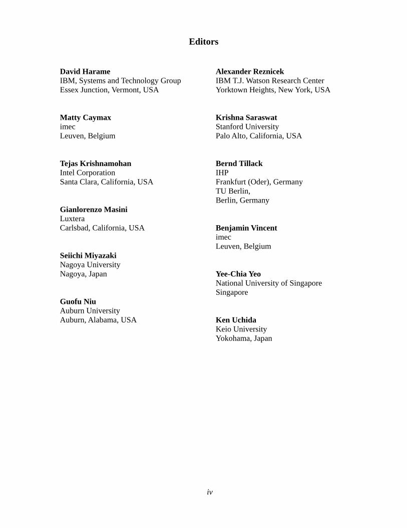
Editors
David Harame IBM, Systems and Technology Group Essex Junction, Vermont, USA Matty Caymax imec Leuven, Belgium Tejas Krishnamohan Intel Corporation Santa Clara, California, USA Gianlorenzo Masini Luxtera Carlsbad, California, USA Seiichi Miyazaki Nagoya University Nagoya, Japan Guofu Niu Auburn University Auburn, Alabama, USA
Alexander Reznicek IBM T.J. Watson Research Center Yorktown Heights, New York, USA Krishna Saraswat Stanford University Palo Alto, California, USA Bernd Tillack IHP Frankfurt (Oder), Germany TU Berlin, Berlin, Germany Benjamin Vincent imec Leuven, Belgium Yee-Chia Yeo National University of Singapore Singapore Ken Uchida Keio University Yokohama, Japan
v
Symposium Organizing Committees
HBT Committee G. Niu, Auburn University, USA (Chair) M. Östling, KTH, Sweden J. Cressler, Georgia Tech, USA A. Chantre, STMicroelectronics, France J. Osten, University of Hannover, Germany D. Knoll, IHP, Germany K. Washio, Tohoku University, Japan A. Joseph, IBM, USA FET Committee Y.C. Yeo, University of Singapore, Singapore
(Chair) K. Rim, IBM, USA T. Tezuka, MIRAI-ASET, Japan J. Hoyt, MIT, USA T. Skotnicki, STMicroelectronics, France S. Deleonibus, LETI, France K. De Meyer, IMEC, Belgium A. Thean, IBM, USA Optoelectronics Committee G. Masini, Luxtera, USA (Chair) G. Flammand, IMEC, Belgium G. Capellini, University of Rome, Italy Y. Kang, Intel, USA K. Wada, Tokyo University and PECST, Japan J. Liu, Dartmouth College, USA S. Assefa, IBM, USA J. Xia, Musashi Institute of Technology, Japan Epitaxy Committee M.R. Caymax, imec, Belgium (Chair) J.M. Hartmann, LETI, France S. Thomas, ASM, USA Y. Kunii, Hitachi Kokusai Electric, Japan M. Sakuraba, Tohoku University, Japan Y. Kim, AMAT, USA Emerging Applications Committee T. Krishnamohan, Intel, USA (Chair) S. Koester, University of Minnesota, USA E. Tutuc, University of Texas Austin, USA M. Eriksson, University of Wisconsin, USA D. Paul, University of Glasgow, Scotland, UK
Processing Committee B. Tillack, IHP, TU Berlin, Germany (Chair) C.-W. Liu, National Taiwan University T. Sadoh, Kyushu University, Japan J.C. Sturm, Princeton University, USA E. Hijzen, NXP Semiconductors, Belgium D. Dutartre, STMicroelectronics, France Strain Layers Committee K. Uchida, Keio University, Japan (Chair) S. Bedell, IBM, USA D. Houghton, AdvanceSis, UK V. Moroz, Synopsys, USA C. Mazure, SOITEC, France R. Loo, IMEC, Belgium Surfaces and Interfaces Committee S. Miyazaki, Nagoya University, Japan
(Chair) S. Zaima, Nagoya University, Japan E. Garfunkel, Rutgers University, USA V. Le Than, CRMS-N/CNRS, France A. Nishiyama, Toshiba Co., Japan P. C. McIntyre, Stanford University, USA Related Compounds Committee A. Reznicek, IBM, USA (Chair) E.A. Fitzgerald, MIT, USA M. Bauer, ASM, USA Y. Cho, AMAT, USA GeSn Sessions and Workshop B. Vincent, imec, Belgium (Chair) S. Koester, University of Minnesota, USA M. Caymax, imec, Belgium K. Rim, IBM, USA Evening Workshop K. Saraswat, Stanford University, USA
(Chair) General Committee J. Murota, Tohoku University, Japan General Symposium Organizer D. Harame IBM, Essex Junction, VT 05452, USA [email protected] Phone +1-802-769-9231
EC
Plati
Go
Silv
CS Electroni
Bron
vi
inum Spon
old Spons
ver Spons
ics and Photo
ze Sponso
nsor
or
ors
onics Divisi
ors
on
vii
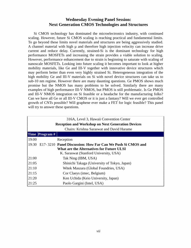
Wednesday Evening Panel Session: Next Generation CMOS Technologies and Structures
Si CMOS technology has dominated the microelectronics industry, with continued
scaling. However, future Si CMOS scaling is reaching practical and fundamental limits. To go beyond these limits novel materials and structures are being aggressively studied. A channel material with high µ and therefore high injection velocity can increase drive current and reduce delay. Currently, strained-Si is the dominant technology for high performance MOSFETs and increasing the strain provides a viable solution to scaling. However, performance enhancement due to strain is beginning to saturate with scaling of nanoscale MOSFETs. Looking into future scaling it becomes important to look at higher mobility materials, like Ge and III-V together with innovative device structures which may perform better than even very highly strained Si. Heterogeneous integration of the high mobility Ge and III-V materials on Si with novel device structures can take us to sub-10 nm regime. However there are many daunting questions. Ge PMOS shows much promise but the NMOS has many problems to be solved. Similarly there are many examples of high performance III-V NMOS, but PMOS is still problematic. Is Ge PMOS and III-V NMOS integration on Si feasible or a headache for the manufacturing folks? Can we have all Ge or all III-V CMOS or it is just a fantasy? Will we ever get controlled growth of CNTs possible? Will graphene ever make a FET for logic feasible? This panel will try to answer these questions.
316A, Level 3, Hawaii Convention Center Reception and Workshop on Next Generation Devices
Chairs: Krishna Saraswat and David Harame Time Program # 19:00 Reception 19:30 E17- 3210 Panel Discussion: How Far Can We Push Si CMOS and
What are the Alternatives for Future ULSI K. Saraswat (Stanford University, USA)
21:00 Tak Ning (IBM, USA) 21:05 Shinichi Takaga (University of Tokyo, Japan) 21:10 Witek Maszara (Global Foundries, USA) 21:15 Cor Claeys (imec, Belgium) 21:20 Ken Uchida (Keio University, Japan) 21:25 Paolo Gargini (Intel, USA)

ix
ECS Transactions, Volume 50, Issue 9 SiGe, Ge, and Related Compounds 5: Materials, Processing, and Devices
Table of Contents
Preface
iii
Chapter 1 Opening and Plenary Session
Monday AM Session Chair: D. Harame 8:25 AM Introductory Remarks
D. Harame (IBM Systems and Technology Group)
(E17-3101) 8:45 AM (Invited) Advanced CMOS Scaling and FinFET Technology
E. J. Nowak (IBM)
3
(E17-3102) 9:40 AM (Invited) FinFET and UTB--How to Make Very Short Channel MOSFETs
C. Hu (University of California, Berkeley)
17
Chapter 2
FET/Strain Session 1: FinFET
Monday AM Session Chair: Y.-C. Yeo (E17-3103) 10:50 AM Effect of Fin Doping Concentration on the Electrical Characteristics of Germanium-on-Insulator Multi-Gate Field-Effect Transistor
B. Liu, X. Gong, C. Zhan, G. Han (National University of Singapore (NUS)), N. Daval, C. Veytizou, D. Delprat, B. Nguyen (Soitec), and Y. Yeo (National University of Singapore (NUS))
23
x
(E17-3104) 11:10 AM Germanium Gate-All-Around pFETs on SOI
H. Chang (GIEE,NTU), S. Hsu, C. Chu (National Nano Device Laboratories), Y. Chen, W. Tu (National Taiwan University), P. Sung, G. Luo (National Nano Device Laboratories), Y. Yin, and C. Liu (National Taiwan University)
31
(E17-3105) 11:30 AM Selective Growth of Strained Ge Channel on Relaxed SiGe Buffer in Shallow Trench Isolation for High Mobility Ge Planar and Fin p-FET
B. Vincent, L. Witters, O. Richard, A. Hikavyy, H. Bender, R. Loo, M. Caymax, and A. Thean (imec)
39
(E17-3106) 11:50 AM Stress Techniques and Mobility Enhancement in FinFET Architectures
G. Eneman, L. Witters, J. Mitard, G. Hellings, A. De Keersgieter (imec), D. P. Brunco (Globalfoundries), A. Hikavyy, B. Vincent, E. Simoen, P. Favia, H. Bender, A. Veloso, T. Chiarella, G. Boccardi, M. Kim, M. Togo, R. Loo, K. De Meyer, N. Horiguchi, N. Collaert, and A. Thean (imec)
47
Chapter 3
HBT Session 1: Advanced SiGe HBT Technology
Monday PM Session Co-Chairs: G. Niu and M. Ostling (E17-3107) 1:40 PM (Invited) Advanced Transistor Architectures for Half-Terahertz SiGe HBTs
B. Heinemann, A. Fox, and H. Rücker (IHP)
61
(E17-3108) 2:10 PM Understanding the Effects of Epitaxy Artifacts on SiGe HBT Performance through Detailed Process/Device Simulation
R. A. Camillo-Castillo (IBM Microelectronics), J. Johnson (IBM Systems and Technology Group), Q. Liu, P. Cheng, J. W. Adkisson (IBM Microelectronics), and D. L. Harame (IBM Systems and Technology Group)
73
xi
(E17-3109) 2:30 PM Improved Frequency Response in a SiGe npn Device through Improved Dopant Activation
J. W. Adkisson (IBM Microelectronics), M. H. Khater (IBM T.J. Watson Research Center), J. P. Gambino, P. Cheng, V. Jain, R. A. Camillo-Castillo (IBM Microelectronics), C. Lavoie (IBM T.J. Watson Research Center), A. Sutton, O. Gluschenkov (IBM Semiconductor Research and Development Center), Q. Liu, T. McDevitt (IBM Microelectronics), S. U. Engelmann (IBM T.J. Watson Research Center), J. J. Pekarik (IBM Microelectronics), and D. L. Harame (IBM Systems and Technology Group)
83
(E17-3110) 2:50 PM Evaluation and Modeling of Relative Importance of RF Noise Sources in SiGe HBTs Using Various Noise Representations
Z. Xu and G. Niu (Auburn University)
95
(E17-3111) 3:10 PM (Invited) Strained Silicon Heterojunction Bipolar Transistors
A. O'Neill (Newcastle University)
109
(E17-3112) 3:40 PM A Self-Aligned Sacrificial Emitter Process for High Performance SiGe HBT in BiCMOS
Q. Liu, J. W. Adkisson (IBM Microelectronics), J. Benoit (IBM Systems and Technology Group), R. A. Camillo-Castillo (IBM Microelectronics), K. K. Chan (IBM Research), P. Cheng (IBM Microelectronics), J. Ellis-Monaghan, T. Gabert (IBM Systems and Technology Group), J. P. Gambino (IBM Microelectronics), P. Gray, J. Hasselbach (IBM Systems and Technology Group), V. Jain (IBM Microelectronics), M. H. Khater (IBM T.J. Watson Research Center), B. Leidy (IBM Systems and Technology Group), D. Park (IBM Research), J. J. Pekarik (IBM Microelectronics), M. Tiersch, C. Willets, B. K. Zetterlund, and D. L. Harame (IBM Systems and Technology Group)
121
xii
Chapter 4 FET/Processing/Strain Session 1: SiGe and Ge Channel FET
Tuesday AM Session Co-Chairs: Y.-C. Yeo and B. Tillack (E17-3113) 8:00 AM (Invited) Implant Free SiGe-Quantum Well: From Device Concept To High-Performing pFETs
J. Mitard, G. Eneman, G. Hellings, L. Witters, A. Hikavyy, B. Vincent, R. Loo, H. Bender, N. Horiguchi, N. Collaert, and A. Thean (imec)
131
(E17-3114) 8:30 AM Effective Condensation Process for Higher Ge Concentration and Thin SiGe layer-on-insulator Substrates in Advanced High Mobility MOSFETs
D. Lee, T. Shim, T. Kim, S. Song, S. Lee (Hanyang University), R. Okuyama (Sumco Corporation), and J. Park (Hanyang University)
n/a
(E17-3115) 8:50 AM SiGe Doped-Channel FET Formed by Sputter Epitaxy Method
M. Yoshikawa, H. Otsuka (Tokyo University of Agriculture & Technology), A. Kasamatsu, N. Hirose, T. Mimura, T. Matsui (National Institute of Information and Communications Technology), and Y. Suda (Tokyo University of Agriculture & Technology)
145
(E17-3116) 9:10 AM Hole Mobility Boost of Ge p-MOSFETs by Composite Uniaxial Stress and Biaxial Strain
H. Lan, Y. Chen, J. Lin, and C. Liu (National Taiwan University)
151
(E17-3117) 9:50 AM (Invited) Modeling of Field-Effect-Transistors with Strained and Alternative Channel Materials
F. Conzatti, D. Esseni, P. Palestri, and L. Selmi (University of Udine)
157
(E17-3118) 10:20 AM Physical Mechanism of Enhanced Uniaxial Stress Effect on Carrier Mobility in ETSOI MOSFETs
T. Ohashi, S. Oda (Tokyo Institute of Technology), and K. Uchida (Keio University)
171
xiii
Chapter 5 Surfaces and Interfaces Session 1
Tuesday AM Session Co-Chairs: S. Miyazaki and S. Zaima (E17-3119) 10:40 AM (Invited) Reliability of SiGe Channel MOS
J. Franco, B. Kaczer, J. Mitard, M. Toledano-Luque, G. Eneman, P. Roussel, M. Cho, T. Kauerauf, L. Witters, A. Hikavyy, G. Hellings, L. Ragnarsson, N. Horiguchi (imec), T. Grasser (T.U. Wien), M. M. Heyns, and G. Groeseneken (imec)
177
(E17-3120) 11:10 AM Evaluation Of Ni(Si1-xGex) and Pt(Si1-xGex) Contact Resistance for FD-SOI PMOS Metallic Source and Drain
E. Bourjot (STMicroelectronics), F. Nemouchi, V. Carron (CEA-LETI), Y. Morand (STMicroelectronics), S. Bernasconi, M. Vinet, J. Damlencourt, F. Allain, O. Cueto, and D. Lafond (CEA-LETI)
197
(E17-3121) 11:30 AM (Invited) Gate Stack and Source/Drain Junction Formations for High-Mobility Ge MOSFETs
H. Nakashima, K. Yamamoto, H. Yang, and D. Wang (Kyushu University)
205
(E17-3122) 12:00 PM Thermally Stable NiSi2 for Ge Contact with Schottky Barrier Height Modulation Capability
R. Yoshihara, Y. Tamura, K. Kakushima, P. Ahmet, Y. Kataoka, A. Nishiyama, N. Sugii, K. Tsutsui, K. Natori, T. Hattori, and H. Iwai (Tokyo Institute of Technology)
217
(E17-3123) 12:20 PM Effect of an Atomically Matched Structure on Fermi-level Pinning at Metal/p-Ge Interfaces
K. Kasahara, H. Yoshioka, Y. Tojo, T. Nishimura, S. Yamada, M. Miyao, and K. Hamaya (Kyushu University)
223
xiv
Chapter 6 Processing Session 1: Strain, Defects, and Diffusion
Tuesday PM Session Co-Chairs: D. Gruetzmacher and A. Sakai (E17-3124) 1:50 PM (Invited) Understanding Diffusion, Activation, and Related Phenomena in SiGe Alloys: Models and Challenges
H. W. Kennel (Intel Corporation)
233
(E17-3125) 2:20 PM (Invited) Strain Control of Si and Si1-x-yGexCy Layers in Si/Si1-x-yGexCy/Si Heterostructures by Low-Pressure Chemical Vapor Deposition
J. Murota, T. Kikuchi, J. Hasegawa, and M. Sakuraba (Tohoku University)
245
(E17-3126) 2:50 PM Phosphorus Profile Control in Ge by Si Delta Layers
Y. Yamamoto, P. Zaumseil, R. Kurps (IHP), J. Murota (Tohoku University), and B. Tillack (IHP)
255
(E17-3127) 3:10 PM Dopant Enhanced Diffusion for High n-typed Doped Ge
Y. Cai, R. E. Camacho-Aguilera, J. T. Bessette, L. C. Kimerling, and J. Michel (Massachusetts Institute of Technology)
263
(E17-3128) 3:30 PM Study of Ge Threading Dislocations Post Growth Treatments
A. Silber and E. Ginsburg (Micron Semiconductors Israel Ltd.)
267
Chapter 7
Optoelectronics Session 1: Solar Cells, Emission, and Photonics
Tuesday PM Session Chair: G. Masini (E17-3129) 1:50 PM (Invited) Ge Optical Emitters Fabricated by Ge Condensation and Epitaxial Growth
K. Oda, K. Tani, S. Saito, and T. Ido (PETRA)
277
xv
(E17-3130) 2:20 PM (Invited) Group-IV Subcells in Multijunction Concentrator Solar Cells
R. R. King, C. Fetzer, P. Chiu, E. Rehder, K. Edmondson, and N. Karam (Spectrolab, Inc.)
287
(E17-3131) 2:50 PM Substrate Design and Thermal Budget Tuning for Integration of Photonic Components in a High-Performance SiGe:C BiCMOS Process
D. Knoll, H. H. Richter, B. Heinemann, S. Lischke, Y. Yamamoto, L. Zimmermann, and B. Tillack (IHP)
297
(E17-3132) 3:10 PM Direct Band-gap Electroluminescence from Strained n-Ge Light Emitting Diodes
P. Velha, K. F. Gallacher, D. C. Dumas, D. J. Paul (University of Glasgow), M. Myronov, and D. R. Leadley (University of Warwick)
305
(E17-3133) 3:30 PM Parameters Controlling Emission of Terahertz Frequency Electromagnetic Radiation from InAs and GaAs: An Ensemble Monte Carlo Simulation Study
D. L. Cortie and R. A. Lewis (University of Wollongong)
309
Chapter 8
Epitaxy Session 1: Pre-epi Si Surface Cleaning and III-V Compound Semiconductor Hetero-epitaxy
Tuesday PM Session Co-Chairs: Y.-C. Yeo and A. Reznicek (E17-3134) 4:05 PM (Invited) Selective-Area Epitaxial Lateral Overgrowth of InGaAs Microdiscs on Si
M. Sugiyama (University of Tokyo)
313
(E17-3135) 4:35 PM (Invited) III-V/GaP Epitaxy on Si for Advanced Photovoltaics and Green Light Emitters
T. J. Grassman, C. Ratcliff, A. M. Carlin, J. A. Carlin, L. Yang, M. J. Mills, and S. A. Ringel (The Ohio State University)
321
(E17-3136) 5:05 PM Controlling Epitaxial GaAsxP1-x/Si1-yGey Heterovalent Interfaces
P. Sharma, T. Milakovich, M. T. Bulsara, and E. A. Fitzgerald (Massachusetts Institute of Technology)
333
xvi
(E17-3137) 5:25 PM High Efficiency Low Temperature Pre-epi Clean Method for Advanced Group IV epi Processing
V. Machkaoutsan (ASM Belgium), K. D. Weeks, M. Bauer (ASM America), J. Maes (ASM Belgium), J. Tolle (ASM America), S. G. Thomas (ASM), A. Alian, A. Hikavyy, and R. Loo (imec)
339
(E17-3138) 5:45 PM Heteroepitaxy of III-V Compound Semiconductors on Silicon for Logic Applications: Selective Area Epitaxy in Shallow Trench Isolation Structures vs. Direct Epitaxy Mediated by Strain Relaxed Buffers
M. Cantoro, C. Merckling, S. Jiang, W. Guo, N. Waldron, H. Bender, A. Moussa, B. Douhard, W. Vandervorst, M. M. Heyns, J. Dekoster, R. Loo, and M. Caymax (imec)
349
Chapter 9 Optoelectronics Session 2: Lasing, Strain and Interconnects
Tuesday PM Session Chair: G. Masini (E17-3139) 4:05 PM (Invited) Electrically Pumped Lasing from Ge-on-Si
J. Michel (Massachusetts Institute of Technology)
359
(E17-3140) 4:35 PM (Invited) Strain Engineering for Optical Gain in Germanium
M. El Kurdi, M. De Kersauson, A. Ghrib (Univ Paris-Sud), M. Prost, S. Sauvage, R. Jakomin, G. Beaudoin, O. Mauguin, L. Largeau, I. Sagnes (CNRS), G. Ndong, M. Chaigneau, R. Ossikovski (Ecole Polytechnique), and P. Boucaud (CNRS)
363
(E17-3141) 5:05 PM (Invited) Silicon Compatible High Performance Optical Interconnect Technology
B. Dutt (APIC Corporation)
371
(E17-3142) 5:25 PM Optical Characterization of Ge-on-Si Grown by using RTCVD
T. Kim, Y. Kil, W. Hong, H. Yang, S. Kang, T. Jeong, and K. Shim (Chonbuk National University)
381
xvii
(E17-3143) 5:45 PM High Extinction Ratio, Low Energy Ge Quantum Well Electro-Absorption Modulator with 23 GHz Bandwidth
G. Isella (Politecnico di Milano), P. Chaisakul, D. Marris-Morini, M. Saïd Rouifed (Univ. Paris-Sud), D. Chrastina, J. Frigerio (L-NESS Dip. di Fisica - Politecnico di Milano), X. Le Roux, S. Edmond, J. Coudevylle, and L. Vivien (Univ. Paris-Sud)
387
Chapter 10
Poster Session
Tuesday 6:00 to 8:00 PM (E17-3144) +Effects of HCl on the Growth of Epitaxial Ge
D. L. Franca (Research Foundation of SUNY)
395
(E17-3145) Analysis of Local Electric Conductive Property for Si Nanowire Models
Y. Ikeda, M. Senami, and A. Tachibana (Kyoto University)
399
(E17-3146) Ge1-xSnx Alloys Pseudomorphically Grown on Ge (001) by Sputtering
H. Pérez Ladrón de Guevara (Universidad de Guadalajara), Á. Rodríguez Vázquez, H. Navarro Contreras, and M. Vidal Borbolla (Universidad Autónoma de San Luís Potosí)
413
(E17-3147) High Quality Silicon Cap Layer for 28nm and Beyond PMOS Processes
C. I. Liao, T. Hsuan, C. Chien, M. Chan, C. Yang, J. Y. Wu (United Microelectronics Corp.), and B. Ramachandran (Applied Materials Inc.)
419
(E17-3148) Accurate Reactive Ion Etching of Si, Ge and P Doped Ge in an SF6-O2 Radio-Frequency Plasma
C. Wongwanitwattana, V. A. Shah, M. Myronov, E. H. Parker, T. E. Whall, and D. R. Leadley (University of Warwick)
425
(E17-3149) Formation of Large Grain SiGe on Insulator by Si Segregation in Seedless-Rapid-Melting Process
R. Kato, M. Kurosawa, R. Matsumura, Y. Tojo, T. Sadoh, and M. Miyao (Kyushu University)
431
xviii
(E17-3150) Direct Measurement of Silicon Strain Induced by Stressed TiNx Stripes Through Raman
Z. Fu, X. Ma, H. Yin, J. Niu, J. Yan (Institute of Microelectronics of Chinese Academy of Sciences), and C. Zhao (Chinese Academy of Sciences)
n/a
(E17-3151) Nano-Engineered Gexsi1-x -On Insulator for Heteroepitaxy
K. Hossain (Amethyst Research Inc), M. C. Debnath, T. D. Mishima, M. B. Santos (University of Oklahoma), and O. W. Holland (Amethyst Research Inc)
437
(E17-3152) NMOS SiP Epitaxy Process - Optimizing Facet Growth
C. I. Liao, C. Chien, M. Chan, C. Yang, J. Y. Wu (United Microelectronics Corp.), C. Chung, and B. Ramachandran (Applied Materials Inc.)
443
(E17-3153) Control of Schottky Barrier Height at Al/p-Ge Junctions by Ultrathin Layer Insertion
A. Ohta, M. Matsui, H. Murakami, S. Higashi (Hiroshima University), and S. Miyazaki (Nagoya University)
449
(E17-3154) Characterization of Resistance-Switching Properties of SiOx Films Using Pt Nanodots Electrodes
K. Makihara, M. Fukushima (Nagoya University), A. Ohta, M. Ikeda (Hiroshima University), and S. Miyazaki (Nagoya University)
459
(E17-3155) X-ray and Raman Characterization of Strained SiGe Layers Treated by Stain Etching
W. Zhou, R. Liang, and L. Yan (Tsinghua National Laboratory for Information, Institute of Microelectronics, Tsinghua University)
465
(E17-3156) Ge-on-Si Bufferless Epitaxial Growth for Photonic Devices
R. E. Camacho-Aguilera, Y. Cai, L. C. Kimerling, and J. Michel (Massachusetts Institute of Technology)
469
(E17-3157) Formation of Large-Grain Ge(111) Films on Insulator by Gold-Induced Layer-Exchange Crystallization at Low Temperature
J. Park, T. Suzuki, M. Kurosawa, M. Miyao, and T. Sadoh (Kyushu University)
475
xix
(E17-3158) Impedance Spectroscopy of GeSn-based Heterostructures
B. Baert (University of Liege), O. Nakatsuka, S. Zaima (Nagoya University), and N. Nguyen (University of Liege)
481
(E17-3159) Improvements in Atomic Layer Deposition Nucleation on Ge(100) and SiGe(100) via HOOH dosing
T. Kaufman-Osborn, J. Lee, K. Kiantaj, and A. Kummel (University of California, San Diego)
n/a
(E17-3160) Orientation Dependence of Si1-xCx:P Growth and the Impact on FinFET Structures
J. Tolle, K. D. Weeks, M. Bauer (ASM America), V. Machkaoutsan, J. Maes (ASM Belgium), M. Togo, S. Brus, A. Hikavyy, and R. Loo (imec)
491
(E17-3161) High Throughput Selective Epitaxial Growth of In Situ Doped SiCP/SiP Layers for NMOS Devices Using a Si3H8/SiH3CH3/PH3/Cl2 Based Cyclic Deposition and Etch Process
M. Bauer (ASM America)
499
(E17-3162) Ge-on-Si: Single-Crystal Selective Epitaxial Growth in a CVD Reactor
A. Sammak, W. De Boer, and L. K. Nanver (Delft University of Technology)
507
(E17-3163) The Structural and Electrical Properties in CeO2 Dielectric on Ge Substrate for MOS Capacitors by Atomic Layer Deposition with Ce(iprCp)3
I. Oh, M. Kim, J. Park (Yonsei University), J. Gatineaub, K. Changhee (K.K. Air Liquide Laboratories), and H. Kim (Yonsei University)
n/a
(E17-3164) Point-of-Use Sampling and Organic Impurity Analysis for Bulk Gases in Semiconductor Processing
J. Park, S. Shin, Y. Lee, P. Jun, and J. Kim (Samsung Electronics Co.,Ltd)
513
(E17-3165) Electronic Band Structure and Effective Masses of Ge1-xSnx Alloys
K. Low, Y. Yang, G. Han (National University of Singapore), W. Fan (Nanyang Technological University), and Y. Yeo (National University of Singapore)
519
xx
(E17-3166) Multi-Wavelength High Resolution Micro-Raman and Optical Reflectance Characterization of Nano-Scale Strained Silicon-on-Insulator Substrates
T. Kim, T. Shim (Hanyang University), W. Yoo (WaferMasters, Inc.), and J. Park (Hanyang University)
n/a
(E17-3167) Theoretical Calculation of Defects Formation Under Thermal Equilibrium in Heavily n-type Doped Germanium
K. Takinai, Y. Ishikawa, and K. Wada (The University of Tokyo)
n/a
(E17-3168) Strain Engineering in GeSnSi Materials
H. H. Radamson, M. Noroozi, A. Jamshidi (Royal Institute of Technology (KTH)), P. E. Thompson (Naval Research Laboratory), and M. Östling (Royal Institute of Technology (KTH))
527
(E17-3169) Optimization of SiC:P Raised Source Drain Epitaxy for Planar 20nm Fully Depleted SOI MOSFET Structures
N. Loubet (STMicroelectronics), T. Nagumo (Renesas), T. Adam (IBM), Q. Liu (STMicroelectronics), M. Raymond (GLOBALFOUNDRIES), K. Cheng, A. Khakifirooz, Z. Zhu (IBM), P. Khare (STMicroelectronics), V. K. Paruchuri (IBM Research), B. Doris (IBM), and R. Sampson (STMicroelectronics)
533
(E17-3170) Effect of B+ Flux on the Electrical Activation of Ultra-Shallow B+ Implants in Ge
B. R. Yates, B. L. Darby (University of Florida), D. H. Petersen, O. Hansen (Technical University of Denmark), R. Lin, P. F. Nielsen (CAPRES A/S), B. L. Doyle (Sandia National Laboratory), A. Kontos (Applied Materials), and K. S. Jones (University of Florida)
543
(E17-3171) Strain Evolution of Si1-xGex Selective Epitaxial Growth in Steps
S. Koo, S. Kim, and D. Ko (Yonsei University)
551
(E17-3172) Formation of Silicene and 2D Si Sheets on Ag(111): Growth Mode, Structural and Electronic Properties
P. Vogt, T. Bruhn (TU-Berlin), A. Resta (CNRS-CINaM), B. Ealet (Aix-Marseille University), P. De Padova (CNR-ISM), and G. Le Lay (Aix-Marseille University)
n/a
xxi
(E17-3173) Investigations on GeO Disproportionation Using X-ray Photoelectron Spectroscopy
S. Wang (Institute of Microelectronics, Chinese Academy of Sciences), H. Liu (Chinese Academy of Sciences), T. Nishimura, K. Nagashio, K. Kita, and A. Toriumi (The University of Tokyo)
557
(E17-3174) Oxidation and Sulfidation of Germanium Surfaces: A Comparative Atomic Level Study of Different Passivation Schemes
C. Fleischmann, K. Schouteden (KU Leuven), M. Houssa (University of Leuven), S. Sioncke, C. Merckling, M. Meuris (imec), P. Hönicke, M. Müller, B. Beckhoff (Physikalisch-Technische Bundesanstalt), C. Van Haesendonck, K. Temst, and A. Vantomme (KU Leuven)
569
Chapter 11 GeSn Session 1: GeSn Photonics
Wednesday AM Session Co-Chairs: B. Vincent and G. Masini (E17-3175) 8:00 AM (Invited) GeSn Photodetection and Electroluminescence Devices on Si
M. Oehme, E. Kasper, and J. Schulze (University of Stuttgart)
583
(E17-3176) 8:30 AM High Performance Group IV Photodiodes with Tunable Absorption Edges based on Ternary SiGeSn Alloys
R. T. Beeler, J. Menéndez, D. J. Smith, and J. Kouvetakis (Arizona State University)
591
(E17-3177) 8:50 AM (Invited) MBE Growth of GeSn and SiGeSn Heterojunctions for Photonic Devices
J. S. Harris, H. Lin, R. Chen, Y. Huo, E. Fei, S. Paik, S. Cho, and T. Kamins (Stanford University)
601
xxii
Chapter 12 Epitaxy Session 2: New Materials
Wednesday AM Session Co-Chairs: Y. Kim and M. Sakuraba (E17-3178) 8:00 AM (Invited) Beyond Graphene: Synthesis of Epitaxial Silicene Sheets
G. Le Lay (Aix-Marseille University), P. De Padova (CNR-ISM), A. Resta (CNRS-CINaM), T. Bruhn, and P. Vogt (TU-Berlin)
609
(E17-3179) 8:30 AM (Invited) Epitaxial Growth of Low Defect SiGe Buffer Layers for Integration of New Materials on 300 mm Silicon Wafers
G. Kozlowski, O. Fursenko, P. Zaumseil, T. Schroeder (IHP), M. Vorderwestner, and P. Storck (Siltronic AG)
613
(E17-3180) 9:00 AM Nano-Synthesis Approach to the Fabrication of Monocrystalline Silicon-like (III-V)yIV5-2y Semiconductors
A. V. Chizmeshya, J. Kouvetakis, G. Grzybowski, R. T. Beeler, and J. Menéndez (Arizona State University)
623
(E17-3181) 9:20 AM (Invited) Undoped Ge Core-Si(Ge) Shell Nanowires: Synthesis, Local Composition and Strain Characterization
S. Hu, I. A. Goldthorpe, A. F. Marshall, and P. C. McIntyre (Stanford University)
635
Chapter 13
Emerging Applications Session 1: Quantum Effects / Spintronics
Wednesday AM Session Chair: T. Krishnamohan (E17-3182) 10:05 AM (Invited) Spin Coherence in Si and Applications to Quantum Information Processing
S. A. Lyon, A. M. Tyryshkin, J. He, and R. M. Jock (Princeton University)
647
xxiii
(E17-3183) 10:35 AM (Invited) Single-Shot Readout of Singlet-Triplet Qubit States in a Si/SiGe Double Quantum Dot
J. R. Prance, Z. Shi, C. B. Simmons, D. E. Savage, M. G. Lagally (University of Wisconsin-Madison), L. R. Schreiber, L. M. Vandersypen (Kavli Institute of Nanoscience, TU Delft), M. Friesen, R. Joynt, S. N. Coppersmith, and M. A. Eriksson (University of Wisconsin-Madison)
655
(E17-3184) 11:05 AM A Design Scheme for Topological Insulators Based Bonds, Bands, Symmetry and Spin Orbit Coupling
C. Felser, L. Müchler, S. Chadov (Max Planck Institute Chemical Physics of Solids), G. Fecher, B. Yan (Johannes Gutenberg-Universität), J. Kübler (Max-Planck-Institut Chemische Physik fester Stoffe), H. Zhang, and S. Zhang (Stanford University)
663
(E17-3185) 11:25 AM Measurement and Control of Individual Electron Spins in Silicon MOS-based Quantum Dots
H. Jiang (UCLA)
n/a
Chapter 14 Surfaces and Interfaces Session 2: Nanowires and New Materials
Wednesday AM Session Co-Chairs: S. Miyazaki and P. McIntyre (E17-3186) 10:05 AM (Invited) Non Planar Non Si CMOS - Challenges and Opportunities
C. Hobbs, K. Ang, R. Hill (SEMATECH), I. Ok (IBM), B. Min (SEMATECH), D. L. Franca (Research Foundation of SUNY), H. Stamper, S. Vivekanand, M. Rodgers, S. Gausepohl (CNSE), P. Kirsch, and R. Jammy (SEMATECH)
669
(E17-3187) 10:35 AM Phonon Dispersion in <100> Si Nanowire Covered with SiO2 Film Calculated by Molecular Dynamics Simulation
T. Watanabe, T. Zushi, M. Tomita, R. Kuriyama, N. Aoki, and T. Kamioka (Waseda University)
673
xxiv
(E17-3188) 10:55 AM (Invited) Electron Transport and Strain Mapping in Ge-SixGe1-x Core-Shell Nanowire Heterostructres
D. C. Dillen (The University of Texas at Austin), J. Nah (Chungnam National University), K. M. Varahramyan, S. K. Banerjee, and E. Tutuc (The University of Texas at Austin)
681
(E17-3189) 11:25 AM Liquid-Phase Deposition of Thin Si and Ge Films Based on Ballistic Electro-reduction
T. Ohta, R. Mentek (Tokyo Univ. of A & T), B. Gelloz (Nagoya University), N. Mori (Osaka Univ.), and N. Koshida (Tokyo University of Agriculture and Technology)
691
(E17-3190) 11:45 AM Evidence of Layer-by-Layer Oxidation of Ge Surfaces by Plasma Oxidation Through Al2O3
R. Zhang, P. Huang, J. Lin, M. Takenaka, and S. Takagi (The University of Tokyo)
699
Chapter 15
Processing Session 2: Germanium and Nanoscaled Devices
Wednesday PM Session Co-Chairs: H. W. Kennel and J. Murota (E17-3191) 1:40 PM (Invited) GOI Substrates: Fabrication and Characterization
A. Sakai, S. Yamasaka, J. Kikkawa, S. Takeuchi, Y. Nakamura (Osaka University), Y. Moriyama, T. Tezuka (GNC, AIST), and K. Izunome (Covalent Silicon Corp.)
709
(E17-3192) 2:10 PM (Invited) Strained Nanoscaled Devices
D. Grützmacher, Q. Zhao, S. Richter, L. Knoll, J. Moers, J. Gerharz, G. Mussler, D. Buca, and S. Mantl (Forschungszentrum Jülich)
727
(E17-3193) 2:40 PM Effect of Two-step Oxidation in Ge Condensation on Surface Roughness Property of Relaxed SiGe layer-on-insulator Substrates
T. Shim, T. Kim, D. Lee (Hanyang University), R. Okuyama (SUMCO Corporation), and J. Park (Hanyang University)
n/a
xxv
(E17-3194) 3:00 PM Electrical Isolation of Dislocations in Ge Layers on Si(001) Substrates through CMOS Compatible Suspended Structures
V. A. Shah, M. Myronov, C. Wongwanitwatana, M. Prest, J. S. Richardson-Bullock, E. H. Parker, T. E. Whall, and D. R. Leadley (University of Warwick)
737
(E17-3195) 3:20 PM Formation of Graded SiGe on Insulator by Segregation-Controlled Rapid-Melting-Growth
R. Matsumura, Y. Tojo, H. Yokoyama, M. Kurosawa, T. Sadoh, and M. Miyao (Kyushu University)
747
(E17-3196) 3:40 PM Modeling Two Dimensional Solid Phase Epitaxial Growth for Patterned Ge Substrates
B. L. Darby, B. R. Yates, A. Kumar (University of Florida), A. Kontos (Applied Materials), R. G. Elliman (Australian National University), and K. S. Jones (University of Florida)
753
Chapter 16 Optoelectronics Session 3: Receivers, Emitters, and Interconnects
Wednesday PM Session Chair: G. Masini (E17-3197) 1:40 PM (Invited) Germanium/Silicon Heterostructures for Terahertz Emission
R. W. Kelsall, V. Dinh, P. Ivanov, A. Valavanis, L. J. Lever, Z. Ikonic (University of Leeds), P. Velha, D. Dumas, K. F. Gallacher, D. J. Paul (University of Glasgow), J. Halpin, M. Myrnov, and D. R. Leadley (University of Warwick)
763
(E17-3198) 2:10 PM (Invited) Ge Photodiodes for CMOS Photonics Optical Engines and Interconnects
S. Sahni and G. Masini (Luxtera)
773
xxvi
(E17-3199) 2:40 PM Long Wavelength ≥1.9 μm Germanium for Optoelectronics Using Process Induced Strain
P. Velha, K. F. Gallacher, D. C. Dumas, D. J. Paul (University of Glasgow), M. Myronov, and D. R. Leadley (University of Warwick)
779
(E17-3200) 3:00 PM Fabrication of Ge-on-Si Substrates for the Integration of High-Quality GaAs Nanostructures on Si
S. Bietti (Universita' degli Studi di Milano-Bicocca), S. Cecchi (Politecnico di Milano), C. Frigeri (CNR-IMEM Parma), E. Grilli (Università di Milano Bicocca), A. Fedorov (IFN-CNR), A. Vinattieri, M. Gurioli (Universita' di Firenze), G. Isella (Politecnico di Milano), and S. Sanguinetti (Universita' degli Studi di Milano-Bicocca)
783
(E17-3201) 3:20 PM Advanced Ge-on-Si Telecommunication Receivers
C. R. Doerr (ACACIA COMMUNICATIONS)
791
Chapter 17
Strain Session 1: Channels, Source/Drain, and GaN
Wednesday PM Session Chair: K. Uchida (E17-3202) 4:15 PM (Invited) Heteroepitaxial Lattice Mismatch Stress Relaxation in Nonpolar and Semipolar GaN by Dislocation Glide
E. C. Young and J. S. Speck (University of California Santa Barbara)
797
(E17-3203) 4:45 PM Channel Strain Evolution of Recessed Source/Drain Si1-xCx Structures by Modifying Scaling Factors
S. Kim, D. Byeon, M. Jung, D. Ko (Yonsei University), S. Chopra, Y. Kim (Applied Materials), and H. Lee (Sungkyunkwan University)
801
(E17-3204) 5:05 PM High Ge Content SiGe Selective Processes for Manufacturing Source/Drain in the Next Generations of pMOS Transistors
A. Hikavyy, W. Vanherle, L. Witters, B. Vincent, J. Dekoster, and R. Loo (imec)
807
xxvii
(E17-3205) 5:25 PM Formation of Uniaxially Strained Si/Ge Channels on SiGe Buffers Strain-Controlled with Selective Ion Implantation
K. Sawano, Y. Hoshi, S. Nagakura (Tokyo City University), K. Arimoto, K. Nakagawa (University of Yamanashi), N. Usami (Tohoku University), and Y. Shiraki (Tokyo City University)
815
Chapter 18
Emerging Applications Session 2: Quantum Effects / Spintronics
Wednesday PM Session Chair: T. Krishnamohan (E17-3206) 4:15 PM (Invited) Coherent Manipulation of a Si/SiGe-based Singlet-Triplet Qubit
E. T. Croke, M. G. Borselli, B. M. Maune, B. Huang, T. D. Ladd, P. W. Deelman, K. S. Holabird, A. A. Kiselev, I. Alvarado-Rodriguez, R. S. Ross, A. E. Schmitz, M. Sokolich, T. M. Hazard, M. F. Gyure, and A. T. Hunter (HRL Laboratories LLC)
823
(E17-3207) 4:45 PM (Invited) Optical Spin Orientation in SiGe Heterostructures
G. Isella, F. Bottegoni, S. Cecchi, A. Ferrari, F. Ciccacci (Politecnico di Milano), F. Pezzoli, A. Giorgioni, E. Gatti, E. Grilli, M. Guzzi (Università di Milano Bicocca), C. Lange, N. Köster, R. Woscholski, S. Chatterjee (Philipps-Universitt Marburg), D. Trivedi, P. Li, Y. Song, and H. Dery (University of Rochester)
831
(E17-3208) 5:15 PM Enhancement-Mode Buried Strained Silicon Channel Double Quantum Dot with Integrated Electrometer
T. Lu (Sandia National Labs), N. Bishop, T. Pluym, P. Kotula, M. Lilly, and M. Carroll (Sandia National Laboratories)
837
(E17-3209) 5:35 PM Local Quantity Analysis of Nanosize Electronics and Spintronics Material
M. Senami and A. Tachibana (Kyoto University)
843
xxviii
Reception and Workshop on Next Generation Devices
Wednesday PM Session Co-Chairs: K. Saraswat and D. Harame see page vii for more details 7:00 PM Reception
(E17-3210) 7:30 PM Panel Discussion: How Far Can We Push Si CMOS and What are the Alternatives for Future ULSI
9:00 to 9:30 PM Speakers
T. Ning (IBM), S. Takaga (University of Tokyo), W. Maszara (Global Foundries), C. Claeys (imec), K. Uchida (Keio University), P. Gargini (Intel)
Chapter 19 GeSn Session 2: GeSn Epitaxy
Thursday AM Session Chair: B. Vincent (E17-3211) 8:00 AM (Invited) Ge1-xSnx Materials: Challenges and Applications
R. Loo, B. Vincent, F. Gencarelli, C. Merckling, A. Kumar, G. Eneman, L. Witters, W. Vandervorst, M. Caymax, M. Heyns, and A. Thean (imec)
853
(E17-3212) 8:30 AM GeSn Alloys on Si Using Deuterated Stannane and Trigermane: Synthesis and Properties
G. Grzybowski, R. T. Beeler, L. Jiang, D. J. Smith, A. V. Chizmeshya, J. Kouvetakis, and J. Menéndez (Arizona State University)
865
(E17-3213) 8:50 AM Crystalline Properties and Strain Relaxation Mechanism of CVD Grown GeSn
F. Gencarelli, B. Vincent (imec), J. Demeulemeester, A. Vantomme (KU Leuven), A. Moussa, A. Franquet, A. Kumar, H. Bender, J. Meersschaut, W. Vandervorst, R. Loo, M. Caymax (imec), K. Temst (KU Leuven), and M. Heyns (imec)
875
xxix
(E17-3214) 9:10 AM Epitaxial Growth of Ge1-xSnx by Reduced Pressure CVD Using SnCl4 and Ge2H6
S. Wirths, D. Buca, A. Tiedemann, B. Holländer, P. Bernardy, T. Stoica, D. Grützmacher, and S. Mantl (Forschungszentrum Jülich)
885
(E17-3215) 9:30 AM Thermal Chemical Vapor Deposition of Epitaxial Germanium Tin Alloys
Y. Huang, C. Wang, M. Jin, E. Sanchez, and Y. Kim (Applied Materials, Inc.)
n/a
Chapter 20 GeSn Session 3: GeSn Epitaxy
Thursday AM Session Chair: B. Vincent (E17-3216) 10:05 AM (Invited) Growth and Optical Properties of Ge1-xSnx Alloy Thin Films with a High Sn Content
S. Zaima, O. Nakatsuka, M. Nakamura (Nagoya University), W. Takeuchi, Y. Shimura, and N. Taoka (Nagoya University)
897
(E17-3217) 10:35 AM Growth of Ge1-xSnx Alloys Using Combined Sources of Solid Tin and Gaseous Germane
S. Su, B. Cheng, D. Zhang, G. Zhang, C. Xue, and Q. Wang (Institute of Semiconductors, Chinese Academy of Sciences)
903
(E17-3218) 10:55 AM Growth and Characterization of Heteroepitaxial Layers of GeSiSn Ternary Alloy
T. Yamaha, O. Nakatsuka (Nagoya University), S. Takeuchi (Covalent Silicon Corp.), W. Takeuchi, N. Taoka (Nagoya University), K. Araki (Covalent Materials Co.), K. Izunome (Covalent Silicon Corp.), and S. Zaima (Nagoya University)
907
(E17-3219) 11:15 AM Single Crystalline GeSn on Silicon by Solid Phase Crystallization
R. R. Lieten, S. Decoster, M. Menghini, J. Seo, A. Vantomme, and J. Locquet (KU Leuven)
915
xxx
(E17-3220) 11:35 AM Tin Deuteride (SnD4) Stabilization
R. F. Spohn and C. B. Richenberg (Praxair, Inc.)
921
Chapter 21 GeSn Session 4: GeSn FET
Thursday PM Session Co-Chairs: B. Vincent and Y.-C. Yeo (E17-3221) 1:10 PM (Invited) Tin-Incorporated Source/Drain and Channel Materials for Field-Effect Transistors
Y. Yeo, G. Han, X. Gong, L. Wang, W. Wang, Y. Yang, P. Guo, B. Liu (National University of Singapore (NUS)), S. Su, G. Zhang, C. Xue (Institute of Semiconductors, Chinese Academy of Sciences), and B. Cheng (State Key Laboratory on Integrated Optoelectronics)
931
(E17-3222) 1:40 PM (Invited) GeSn Channel n and p MOSFETs
S. Gupta, R. Chen (Stanford University), B. Vincent, D. Lin (imec), B. Magyari-Kope (Stanford University), M. Caymax, J. Dekoster (imec), J. S. Harris, Y. Nishi, and K. C. Saraswat (Stanford University)
937
(E17-3223) 2:10 PM High Hole Mobility in Strained Germanium-Tin (GeSn) Channel pMOSFET Fabricated on (111) Substrate
G. Han (National University of Singapore (NUS)), S. Su (Institute of Semiconductors, Chinese Academy of Sciences), Y. Yang, P. Guo, X. Gong, L. Wang, W. Wang, C. Guo (National University of Singapore (NUS)), G. Zhang, C. Xue, B. Cheng (Institute of Semiconductors, Chinese Academy of Sciences), and Y. Yeo (National University of Singapore (NUS))
943
(E17-3224) 2:30 PM Fabrication and Negative Bias Temperature Instability (NBTI) Study on Ge0.97Sn0.03 P-MOSFETs with Si2H6 Passivation and HfO2 High-k and TaN Metal Gate
X. Gong (National University of Singapore (NUS)), S. Su (Institute of Semiconductors, Chinese Academy of Sciences), B. Liu, L. Wang, W. Wang, Y. Yang, R. Cheng, E. Kong (National University of Singapore (NUS)), B. Cheng (Institute of Semiconductors, Chinese Academy of Sciences), G. Han, and Y. Yeo (National University of Singapore (NUS))
949
xxxi
Chapter 22 Emerging Applications Session 3: Novel Devices and Memories
Thursday PM Session Chair: T. Krishnamohan (E17-3225) 3:05 PM Si/SiGe Thermoelectric Generators
D. J. Paul, A. Samarelli, L. Ferre Llin, Y. Zhang, J. M. Weaver, P. S. Dobson (University of Glasgow), S. Cecchi (Politecnico di Milano), J. Frigerio, F. Isa (L-NESS, Politecnico di Milano), D. Chrastina (L-NESS Dip. di Fisica - Politecnico di Milano), G. Isella (Politecnico di Milano), T. Etzelstorfer, J. Stangl (Johannes Kepler Universität), and E. Müller Gubler (ETH Zurich)
959
(E17-3226) 3:25 PM SiGe Band-to-Band Tunneling Calibration based on p-i-n Diodes: Fabrication, Measurement and Simulation
K. Kao, A. Verhulst, R. Rooyackers, A. Hikavyy, E. Simoen, K. Arstila, B. Douhard, R. Loo, A. M. Simoen (imec), J. Tolle (ASM America), H. Dekkers (imec), V. Machkaoutsan, J. Maes (ASM Belgium), K. De Meyer, N. Collaert, M. Heyns, C. Huyghebaert, and A. Thean (imec)
965
(E17-3227) 3:45 PM Tunneling Field-Effect Transistor (TFET) with Novel Ge/In0.53Ga0.47As Tunneling Junction
P. Guo, Y. Yang (National University of Singapore), Y. Cheng (Institute of Materials Research and Engineering), G. Han (National University of Singapore), C. Chia (Institute of Materials Research and Engineering), and Y. Yeo (National University of Singapore)
971
(E17-3228) 4:05 PM Germanium Tin Tunneling Field Effect Transistor for Sub-0.4 V Operation
Y. Yang, K. Low, P. Guo, W. Wang, G. Han, and Y. Yeo (National University of Singapore)
979
(E17-3229) 4:25 PM Si/SiGe Tunneling Static Random Access Memories
G. Ternent and D. J. Paul (University of Glasgow)
987
(E17-3230) 4:45 PM Ge Surface-Energy-Driven Secondary Grain Growth for Vertical Channel in 3D NAND Flash Memories
S. Lee, Y. Son, and E. Yoon (Seoul National University)
991
xxxii
Chapter 23 Epitaxy Session 3: In Situ Doping of Si, SiGe, and Ge Epilayers
Thursday PM Session Co-Chairs: R. Loo and B. Tillack (E17-3231) 3:05 PM Epitaxial Growth and Applications of Low-Resistivity Phosphorous-Doped Si1-xCx
T. N. Adam (University at Albany), N. Loubet (STMicroelectronics), A. Reznicek, V. Paruchuri (IBM Research), R. Sampson (STMicroelectronics), and D. Sadana (IBM Research)
n/a
(E17-3232) 3:35 PM Selective Epitaxial Growth of Heavily Boron-Doped Silicon with Uniform Doping Depth Profile
Z. Zhu, Z. Cong, and B. Ramachandran (Applied Materials Inc.)
999
(E17-3233) 3:55 PM High Tensile Strained In-Situ Phosphorus Doped Silicon Epitaxial Film for nMOS Applications
Z. Ye, S. Chopra, R. Lapena, Y. Kim, and S. Kuppurao (Applied Materials)
1007
(E17-3234) 4:15 PM (Invited) Microstructure Development in Epitaxially Grown In Situ Boron and Carbon Co-Doped Strained 60% Silicon-Germanium Layers
A. Reznicek (IBM Research), T. N. Adam (University at Albany), J. Li, Z. Zhu, R. Murphy (IBM Semiconductor Research and Development Center), S. W. Bedell, V. Paruchuri, and D. K. Sadana (IBM T.J. Watson Research Center)
1013
(E17-3235) 4:35 PM In Situ Boron (B) Doped Germanium (Ge:B) Grown on (100), (110), and (111) Silicon: Crystal Orientation and B Incorporation Effects
G. Han, Q. Zhou, P. Guo, W. Wang, Y. Yang, and Y. Yeo (National University of Singapore)
1025
xxxiii
Chapter 24 Related Compounds Session 1: Heterogeneous Integration
Friday AM Session Chair: A. Reznicek (E17-3236) 8:00 AM (Invited) Materials Integration for III-V/SiGe+CMOS Integrated Circuit Platforms
E. A. Fitzgerald (Massachusetts Institute of Technology)
1033
(E17-3237) 8:30 AM (Invited) Heterogeneous Integration of III-V Devices and Si CMOS on a Silicon Substrate
T. E. Kazior (Raytheon), J. LaRoche, and W. Hoke (Raytheon Integrated Defense Systems)
1039
(E17-3238) 9:00 AM (Invited) Heterogeneous Integration of InP HBTs on CMOS: Leveraging and Providing Value to Conventional Silicon Technologies
J. C. Li, Y. Royter, P. Patterson, T. Hussain, J. R. Duvall, M. C. Montes, I. Valles, F. Ku, M. F. Boag-O'Brien, A. Lopez, D. Le, D. Zehnder, S. Kim, S. T. Chen, T. Oh, M. Akmal, E. F. Wang, D. A. Hitko, M. Sokolich, D. H. Chow, P. D. Brewer, and K. R. Elliott (HRL Laboratories LLC)
1047
(E17-3239) 9:30 AM (Invited) Hybrid Wafer Bonding and Heterogeneous Integration of GaN HEMTs and Si (100) MOSFETs
H. Lee, Z. Li, M. Sun, K. Ryu, and T. Palacios (Massachusetts Institute of Technology)
1055
Chapter 25
Related Compounds Session 2: Processing
Friday AM Session Chair: A. Reznicek (E17-3240) 10:15 AM (Invited) Scalable GaN-on-Silicon Using Rare Earth Oxide Buffer Layers
F. Arkun, M. Lebby, R. Dargis, R. Roucka, R. S. Smith, and A. Clark (Translucent Inc.)
1065
xxxiv
(E17-3241) 10:45 AM Formation and Characterization of Nickel Germanosilicide on Si1-xGex/Si/SiO2/Si
W. Yoo (WaferMasters, Inc.), N. Hasuike, H. Harima, and M. Yoshimoto (Kyoto Institute of Technology)
1073
(E17-3242) 11:05 AM Low Specific Ohmic Contacts to n-type Germanium Using a Low Temperature NiGe Process
K. F. Gallacher, P. Velha, D. J. Paul, I. Maclaren (University of Glasgow), M. Myronov, and D. R. Leadly (University of Warwick)
1081
(E17-3243) 11:25 AM Formation of 1.7-nm-thick-EOT Germanium Dioxide Film with a High-Quality Interface Using a Direct Neutral Beam Oxidation Process
A. Wada (Tohoku University), R. Zhang, S. Takagi (The University of Tokyo), and S. Samukawa (Tohoku University)
1085
Author Index 1091
Facts about ECSThe Electrochemical Society (ECS) is an international, nonprofi t, scientifi c, educational organization founded for the advancement of the theory and practice of electrochemistry, electronics, and allied subjects. The Society was founded in Philadelphia in 1902 and incorporated in 1930. There are currently over 7,000 scientists and engineers from more than 70 countries who hold individual membership; the Society is also supported by more than 100 corporations through Corporate Memberships.
The technical activities of the Society are carried on by Divisions. Sections of the Society have been organized in a number of cities and regions. Major international meetings of the Society are held in the spring and fall of each year. At these meetings, the Divisions and Groups hold general sessions and sponsor symposia on specialized subjects.
The Society has an active publication program that includes the following:
Journal of The Electrochemical Society — (JES) is the leader in the fi eld of electrochemical science and technology. This peer-reviewed journal publishes an average of 550 pages of 85 articles each month. Articles are published online as soon as possible after undergoing the peer-review process. The online version is considered the fi nal version and is fully citable with articles assigned specifi c page numbers within specifi c issues. The date of online publication is the offi cial publication date of record.
Journal of Solid State Science and Technology — (JSS) is one of the newest peer-reviewed journals from ECS launched in 2012. JSS covers fundamental and applied areas of solid state science and technology including experimental and theoretical aspects of the chemistry and physics of materials and devices. Articles are published online as soon as possible after undergoing the peer-review process. The online version is considered the fi nal version and is fully citable with articles assigned specifi c page numbers within specifi c issues. The date of online publication is the offi cial publication date of record.
Electrochemistry Letters — (EEL) is one of the newest journals from ECS launched in 2012. It is dedicated to the rapid dissemination of peer-reviewed and concise research reports in fundamental and applied areas of electrochemical science and technology. Articles are published online as soon as possible after undergoing the peer-review process. The online version is considered the fi nal version and is fully citable with articles assigned specifi c page numbers within specifi c issues. The date of online publication is the offi cial publication date of record.
Solid State Letters — (SSL) is one of the newest journals from ECS launched in 2012. It is dedicated to the rapid dissemination of peer-reviewed and concise research reports in fundamental and applied areas of solid state science and technology. Articles are published online as soon as possible after undergoing the peer-review process. The online version is considered the fi nal version and is fully citable with articles assigned specifi c page numbers within specifi c issues. The date of online publication is the offi cial publication date of record.
Electrochemical and Solid-State Letters — (ESL) was the fi rst rapid-publication electronic journal dedicated to covering the leading edge of research and development in the fi eld of solid-state and electrochemical science and technology. ESL was a joint publication of ECS and IEEE Electron Devices Society. Volume 1 began July 1998 and contained six issues, thereafter new volumes began with the January issue and contained 12 issues. The fi nal issue of ESL was Volume 16, Number 6, 2012. Preserved as an archive, ESL has since been replaced by SSL and EEL.
Interface— Interface is an authoritative yet accessible publication for those in the fi eld of solid-state and electrochemical science and technology. Published quarterly, this four-color magazine contains technical articles about the latest developments in the fi eld, and presents news and information about and for members of ECS.
ECS Meeting Abstracts— ECS Meeting Abstracts contain extended abstracts of the technical papers presented at the ECS biannual meetings and ECS-sponsored meetings. This publication offers a fi rst look into the current research in the fi eld. ECS Meeting Abstracts are freely available to all visitors to the ECS Digital Library.
ECS Transactions— (ECST) is the online database containing full-text content of proceedings from ECS meetings and ECS-sponsored meetings. ECST is a high-quality venue for authors and an excellent resource for researchers. The papers appearing in ECST are reviewed to ensure that submissions meet generally-accepted scientifi c standards. Each meeting is represented by a volume and each symposium by an issue.
Monograph Volumes — The Society sponsors the publication of hardbound monograph volumes, which provide authoritative accounts of specifi c topics in electrochemistry, solid-state science, and related disciplines.
For more information on these and other Society activities, visit the ECS website:
www.electrochem.org

Related Documents