p. 1 ISSCC – Feb2008

Welcome message from author
This document is posted to help you gain knowledge. Please leave a comment to let me know what you think about it! Share it to your friends and learn new things together.
Transcript
p. 1
ISSCC – Feb2008
p. 2
A 4 bits per cell 8Gb NROM Data-Storage Memory with Enhanced Write Performance
Ran Sahar1, Avi Lavan1, Eran Geyari1, Amit Berman1,
Itzic Cohen1, Ori Tirosh1, Kobi Danon1, Amichai Givant1
Yoram Betser1, Alexander Kushnarenko1, Yaal Horesh1,
Boaz Eitan1,Yair Sofer1, Ron Eliyahu1 , Eduardo Maayan1,
Wang Pei Jen2, Yan Feng2, Lin Ching Yao2, Kwon Yi Jin2,
Kwon Sung Woo2, Cai En Jing2, Yi Jing Jing2,
Kim Jong Oh2, Yi Guan Jiun2
1 Saifun Semiconductors Ltd. Israel,
2 SMIC International Co. Ltd. China

p. 3
Agenda
• The QUAD NROM Basics & Challenges
• General Architecture
• Multi Level Parallel Program & Verify
• Read & Sensing Method
• Constant Current Erase Technique
• Summary
p. 4
• The QUAD NROM Basics & Challenges
• General Architecture
• Multi Level Parallel Program & Verify
• Read & Sensing Method
• Constant Current Erase Technique
• Summary

p. 5
The Quad NROM Basics
• Two storage areas per cell
• Each storage area is Multi-Level
Bit 1 & Bit 2 Bit 3 & Bit 4
11 01 00 10
Four bits per cell
• Two phase Program algorithm
• Error Detection + Moving Read algorithmReliability

p. 6
The Write Performance Challenges
• Fast Programming & Narrow Vt distributions
• Parallel Programming and Verify algorithm
• Multiple Bit Line Voltage Programming
• Fast Erase with no over erase
• Constant current Erase algorithm
• Fast and reliable Read
Page program speed >4.5MB/s
Program Vt distribution <350mV

p. 7
• The QUAD NROM Basics & Challenges
• General Architecture
• Multi Level Parallel Program & Verify
• Read & Sensing Method
• Constant Current Erase Technique
• Summary
p. 8
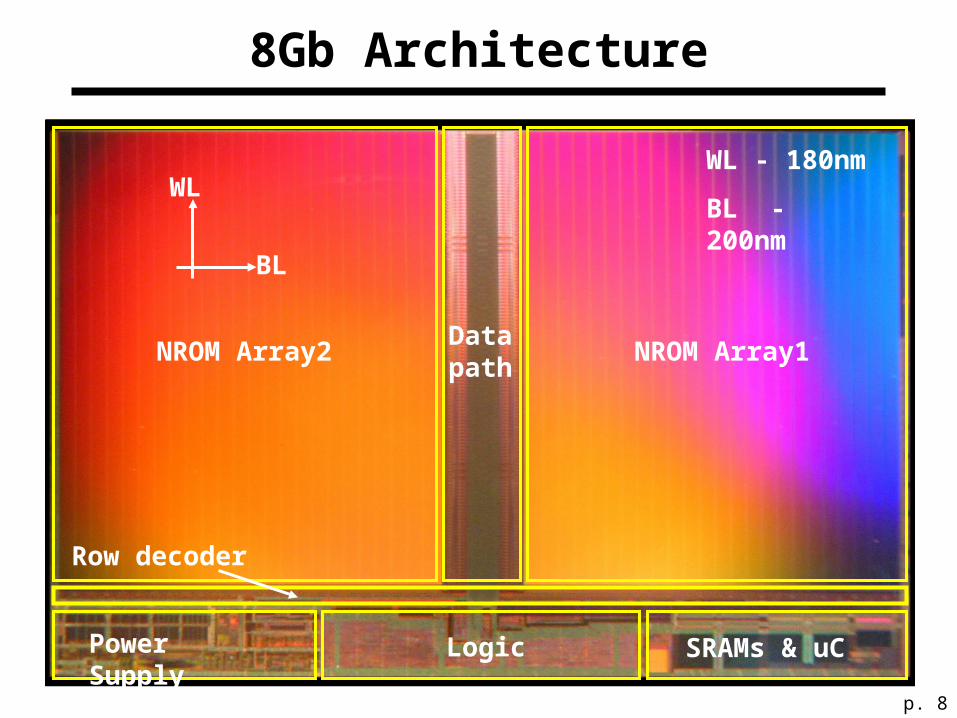
8Gb Architecture
Logic
Row decoder
Data path
SRAMs & uCPower Supply
NROM Array2 NROM Array1
BL
WLWL - 180nm
BL - 200nm

p. 9
• The QUAD NROM Basics & Challenges
• General Architecture
• Multi Level Parallel Program & Verify
• Read & Sensing Method
• Constant Current Erase Technique
• Summary

p. 10
Accessing the Array for Programming
0V
VPGM
0V
0V
SELECT transistors area
ISO
LA
TIO
N
ISO
LA
TIO
N
ISO
LA
TIO
N
ISO
LA
TIO
N
ISO
LA
TIO
N
ISO
LA
TIO
N
ISO
LA
TIO
N
ISO
LA
TIO
N
SELECT transistors area
BL Driver BL Driver
• The challenge for fast program
• Many “bits” to be programmed
• Different target Vt & different “bits” conditions• Different target Vt – e.g. 01, 00, 10• Different conditions – “other half cell” having one of
11, 01, 00, 10 target Vt
p. 11
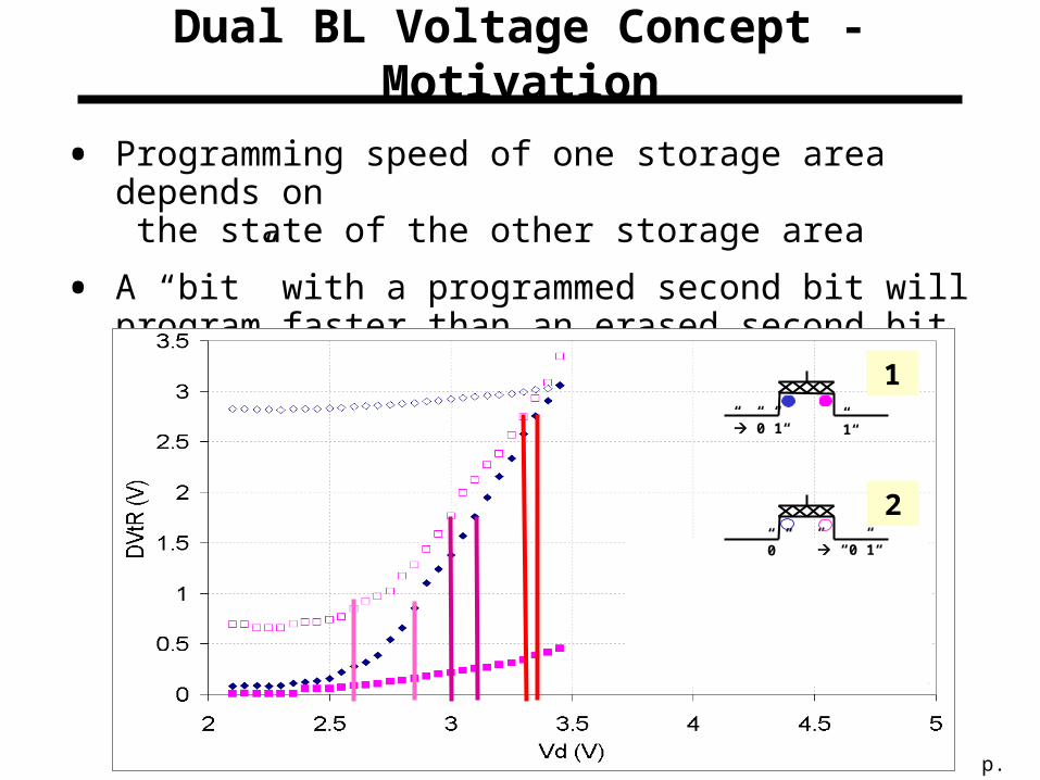
Dual BL Voltage Concept - Motivation
• Programming speed of one storage area depends on the state of the other storage area
• A “bit” with a programmed second bit will program faster than an erased second bit
“1”“1””0”
“1” “0””0”
1
2

p. 12
Parallel Program Principles
• QUAD programming uses different BL voltages (VPPD) per level:
• Level “01” is programmed via VPPD01_1, VPPD01_2
• Level “00” is programmed via VPPD00_1, VPPD00_2
• Level “10” is programmed via VPPD10_1, VPPD10_2
’10’’00’’01’’11’
VPPD01_1VPPD01_
2
VPPD00_1VPPD00_
2
VPPD10_1VPPD10_
2
• All levels end programming at the same time
• Minimal number of pulses

p. 13
Hex Bit Line Driver Circuit
Pre-charge
Gn_2
Gn_1
VDD SF_bias - Vt
Driver Sequence
BL_PGM
BL_PGM
LV
L_
MU
X
VPPD01_1in
LVL_01
LVL_00
VPPD_1_2
VPPD01_2in
VPPD00_1inVPPD00_2in
VPPD10_1inVPPD10_2in
PS_BLOCK
LS
LS
LS
LS
LSLS
LVL_10
Drain_Charge_PumpSF_bias
Pre-charge
Gn_1
Gn_2
VDD

p. 14
Parallel Program-Verify Principles
SA
Ref 10 Ref 00 Ref 01
SA SA
Array Data
SA
FF
latch
latch
latch
Verified DataMUX
Expected Data
Reference SAs
Bit Slice[255]
• All Program levels are verified simultaneously
• Based on the expected data, the correct Verify level is selected

p. 15
• The QUAD NROM Basics & Challenges
• General Architecture
• Multi Level Parallel Program & Verify
• Read & Sensing Method
• Constant Current Erase Technique
• Summary

p. 16
Sensing Method & Read
• Sensing Method:
• Drain sensing – High Accuracy
• VDD driven sensing – Low Power
• All levels sensed at once – High Speed
• Read Challenges:
• Process parameters variations
• Virtual Ground array effects
• Data pattern dependencies Read margin loss
p. 17
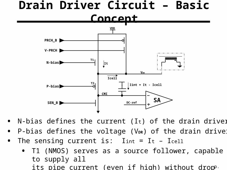
Drain Driver Circuit – Basic Concept
• N-bias defines the current (It) of the drain driver
• P-bias defines the voltage (VDR) of the drain driver
• The sensing current is: Iint = It – Icell
• T1 (NMOS) serves as a source follower, capable to supply all its pipe current (even if high) without drop penalty
VDD
N-bias
P-bias
SEN_B
It
Iint = It - Icell
Icell
T1
T2
V-PRCH
PRCH_B
SADC-ref
VDR
CMI

p. 18
Sense Amplifier with Offset Cancellation
Operation :
1. Offset cancellation period: o1 & in1 are shorted Left plate of C is at DC_Ref, o1 & in1 at inverter’s trip point
2. Initialization period: SA_IN & in are discharged to GND in1 follows by C coupling to Vtrip_point – DC_Ref
3. NROM cell signal integration period: SA_IN integrates from GND Outputs (o1& o2) will flip when SA_IN crosses DC_Ref
PRCH_B
CMI
SA Out
DC_ref
SEN_B Stabilization
OFC_EN Offset Cancellation
Sensing
SA_IN
OFC_EN
NBIAS
SA_IN_ON
OFC_EN_B
C
in in1
o1 o2
DC_Ref
CMI

p. 19
The Virtual Ground Pipe Effect
• Pipe current should be minimized!
• Achieved by a Proper Physical order sequence
Icell1 = Icell2, Ipipe1 > Ipipe2 (Different neighbors state)
Isense1 < Isense2
I_sense1
Ipipe1 Icell1
I_sense2
Ipipe2 Icell2
Erase
Program
p. 20
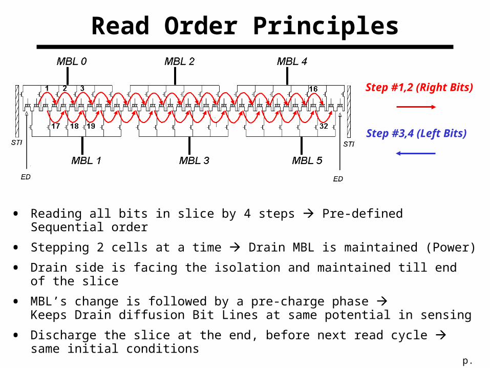
Read Order Principles
• Reading all bits in slice by 4 steps Pre-defined Sequential order
• Stepping 2 cells at a time Drain MBL is maintained (Power)
• Drain side is facing the isolation and maintained till end of the slice
• MBL’s change is followed by a pre-charge phase Keeps Drain diffusion Bit Lines at same potential in sensing
• Discharge the slice at the end, before next read cycle same initial conditions
Step #1,2 (Right Bits)
Step #3,4 (Left Bits)
p. 21
• The QUAD NROM Basics & Challenges
• General Architecture
• Multi Level Parallel Program & Verify
• Read & Sensing Method
• Constant Current Erase Technique
• Summary

p. 22
Accessing the Array for Erase
• The challenge for fast erase
• Many cells to be Erased Too high current consumption
• The Erase mechanism - TEHH band to band
• Peak Erase current suppression is necessary for erase parallelism
SELECT transistors area
ISO
LA
TIO
N
ISO
LA
TIO
N
ISO
LA
TIO
N
ISO
LA
TIO
N
ISO
LA
TIO
N
ISO
LA
TIO
N
ISO
LA
TIO
N
ISO
LA
TIO
N
SELECT transistors area
BL Driver BL Driver
p. 23
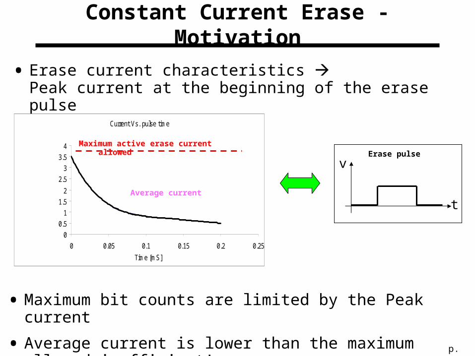
Constant Current Erase - Motivation
• Erase current characteristics Peak current at the beginning of the erase pulse
• Maximum bit counts are limited by the Peak current
• Average current is lower than the maximum allowed-inefficient!
Current Vs. pulse time
0
0.5
1
1.5
2
2.5
3
3.5
4
0 0.05 0.1 0.15 0.2 0.25
Time [mS]
Current [mA]
t
v
Maximum active erase current allowedErase pulse
Average current

p. 24
Constant Current Erase - Technique
• Implement an erase pulse shape, that will enable the erasure of maximum bit count, within the limitation of the erase active maximum current
• Bit Line erase voltage will be ramped to the target voltage level
• Charge Pump current is continuously monitored and the voltage ramp rate adjusted, to prevent current from exceeding the specified limit
t
V Erase Pulse
Hold time
VPPD step sizeVPPD Initial
• Parameters for optimization: Bit count, target VPPD level, initial VPPD level

p. 25
Constant current Erase - Product Results
Charge pump
Active Current
EV
Figure 1
Figure 1: VPPD target is increased according to algorithm, active current is following the VPPD increment, Charge pump is constant for each erase pulse phase
Figure 2: VPPD rises only when Active current is lower than the maximum current allowed
VPPD Active Current
Figure 2
p. 26
• The QUAD NROM Basics & Challenges
• General Architecture
• Multi Level Parallel Program & Verify
• Read & Sensing Method
• Constant Current Erase Technique
• Summary
p. 27
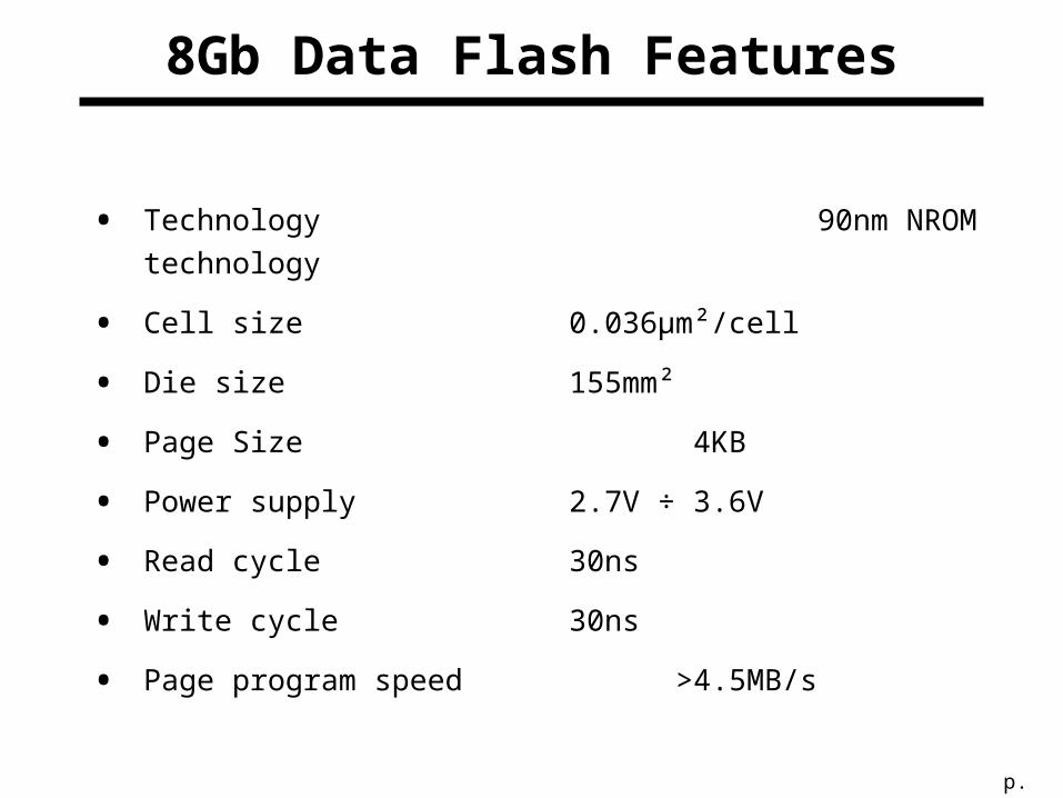
8Gb Data Flash Features
• Technology 90nm NROM technology
• Cell size 0.036µm²/cell
• Die size 155mm²
• Page Size 4KB
• Power supply 2.7V ÷ 3.6V
• Read cycle 30ns
• Write cycle 30ns
• Page program speed >4.5MB/s
p. 28
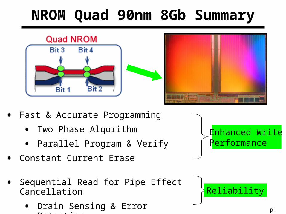
NROM Quad 90nm 8Gb Summary
• Fast & Accurate Programming
• Two Phase Algorithm
• Parallel Program & Verify
• Constant Current Erase
• Sequential Read for Pipe Effect Cancellation
• Drain Sensing & Error Detection
Enhanced Write Performance
Reliability

p. 29