To learn more about ON Semiconductor, please visit our website at www.onsemi.com Please note: As part of the Fairchild Semiconductor integration, some of the Fairchild orderable part numbers will need to change in order to meet ON Semiconductor’s system requirements. Since the ON Semiconductor product management systems do not have the ability to manage part nomenclature that utilizes an underscore (_), the underscore (_) in the Fairchild part numbers will be changed to a dash (-). This document may contain device numbers with an underscore (_). Please check the ON Semiconductor website to verify the updated device numbers. The most current and up-to-date ordering information can be found at www.onsemi.com. Please email any questions regarding the system integration to [email protected]. Is Now Part of ON Semiconductor and the ON Semiconductor logo are trademarks of Semiconductor Components Industries, LLC dba ON Semiconductor or its subsidiaries in the United States and/or other countries. ON Semiconductor owns the rights to a number of patents, trademarks, copyrights, trade secrets, and other intellectual property. A listing of ON Semiconductor’s product/patent coverage may be accessed at www.onsemi.com/site/pdf/Patent-Marking.pdf. ON Semiconductor reserves the right to make changes without further notice to any products herein. ON Semiconductor makes no warranty, representation or guarantee regarding the suitability of its products for any particular purpose, nor does ON Semiconductor assume any liability arising out of the application or use of any product or circuit, and specifically disclaims any and all liability, including without limitation special, consequential or incidental damages. Buyer is responsible for its products and applications using ON Semiconductor products, including compliance with all laws, regulations and safety requirements or standards, regardless of any support or applications information provided by ON Semiconductor. “Typical” parameters which may be provided in ON Semiconductor data sheets and/or specifications can and do vary in different applications and actual performance may vary over time. All operating parameters, including “Typicals” must be validated for each customer application by customer’s technical experts. ON Semiconductor does not convey any license under its patent rights nor the rights of others. ON Semiconductor products are not designed, intended, or authorized for use as a critical component in life support systems or any FDA Class 3 medical devices or medical devices with a same or similar classification in a foreign jurisdiction or any devices intended for implantation in the human body. Should Buyer purchase or use ON Semiconductor products for any such unintended or unauthorized application, Buyer shall indemnify and hold ON Semiconductor and its officers, employees, subsidiaries, affiliates, and distributors harmless against all claims, costs, damages, and expenses, and reasonable attorney fees arising out of, directly or indirectly, any claim of personal injury or death associated with such unintended or unauthorized use, even if such claim alleges that ON Semiconductor was negligent regarding the design or manufacture of the part. ON Semiconductor is an Equal Opportunity/Affirmative Action Employer. This literature is subject to all applicable copyright laws and is not for resale in any manner.

Welcome message from author
This document is posted to help you gain knowledge. Please leave a comment to let me know what you think about it! Share it to your friends and learn new things together.
Transcript

To learn more about ON Semiconductor, please visit our website at www.onsemi.com
Please note: As part of the Fairchild Semiconductor integration, some of the Fairchild orderable part numbers will need to change in order to meet ON Semiconductor’s system requirements. Since the ON Semiconductor product management systems do not have the ability to manage part nomenclature that utilizes an underscore (_), the underscore (_) in the Fairchild part numbers will be changed to a dash (-). This document may contain device numbers with an underscore (_). Please check the ON Semiconductor website to verify the updated device numbers. The most current and up-to-date ordering information can be found at www.onsemi.com. Please email any questions regarding the system integration to [email protected].
Is Now Part of
ON Semiconductor and the ON Semiconductor logo are trademarks of Semiconductor Components Industries, LLC dba ON Semiconductor or its subsidiaries in the United States and/or other countries. ON Semiconductor owns the rights to a number of patents, trademarks, copyrights, trade secrets, and other intellectual property. A listing of ON Semiconductor’s product/patent coverage may be accessed at www.onsemi.com/site/pdf/Patent-Marking.pdf. ON Semiconductor reserves the right to make changes without further notice to any products herein. ON Semiconductor makes no warranty, representation or guarantee regarding the suitability of its products for any particular purpose, nor does ON Semiconductor assume any liability arising out of the application or use of any product or circuit, and specifically disclaims any and all liability, including without limitation special, consequential or incidental damages. Buyer is responsible for its products and applications using ON Semiconductor products, including compliance with all laws, regulations and safety requirements or standards, regardless of any support or applications information provided by ON Semiconductor. “Typical” parameters which may be provided in ON Semiconductor data sheets and/or specifications can and do vary in different applications and actual performance may vary over time. All operating parameters, including “Typicals” must be validated for each customer application by customer’s technical experts. ON Semiconductor does not convey any license under its patent rights nor the rights of others. ON Semiconductor products are not designed, intended, or authorized for use as a critical component in life support systems or any FDA Class 3 medical devices or medical devices with a same or similar classification in a foreign jurisdiction or any devices intended for implantation in the human body. Should Buyer purchase or use ON Semiconductor products for any such unintended or unauthorized application, Buyer shall indemnify and hold ON Semiconductor and its officers, employees, subsidiaries, affiliates, and distributors harmless against all claims, costs, damages, and expenses, and reasonable attorney fees arising out of, directly or indirectly, any claim of personal injury or death associated with such unintended or unauthorized use, even if such claim alleges that ON Semiconductor was negligent regarding the design or manufacture of the part. ON Semiconductor is an Equal Opportunity/Affirmative Action Employer. This literature is subject to all applicable copyright laws and is not for resale in any manner.

FPF2300/02/03 D
ual-Output C
urrent Limit Sw
itch
June 2009
© 2009 Fairchild Semiconductor Corporation www.fairchildsemi.com
FPF2300/02/03 Rev. 1.1.3
FPF2300/02/03 Dual-Output Current Limit SwitchFeatures ! 1.8 to 5.5V Input Voltage Range ! Typical RON = 75mΩ at IN = 5.5V! 1.3A Current Limit (Typical)! Slew Rate Controlled! Reversed Current Blocking when Disabled! ESD Protected, Above 4000V HBM! Independent Thermal Shutdown! UVLO! RoHS Compliant
Applications ! Notebook Computing! Peripheral USB Ports! Networking / USB Based Equiptment
DescriptionThe FPF2300/02/03 are dual-channel load switches ofIntelliMAX family. The FPF2300/02/03 consist of dual,independent, current-limited, slew rate controlled, P-channel MOSFET power switches. Slew rated turn-onprevents inrush current from glitching supply rails. Theinput voltage range operates from 1.8V to 5.5V to fulfilltoday's USB device supply requirements. Switch controlis accomplished by a logic input (ON) capable ofinterfacing directly with low-voltage control signal.
For the FPF2302, if the constant current condition per-sists after 10ms, these parts shut down the switch andpull the fault signal pin (FLAGB) LOW. The FPF2300 hasan auto-restart feature that turns the switch on againafter 504ms if the ON pin is still active. For the FPF2303,a current limit condition immediately pulls the fault signalpin LOW and the part remains in the constant-currentmode until the switch current falls below the current limit.For the FPF2300 through FPF2303, the current limit istypically 1.3A for each switch to align with notebookcomputing applications. FPF2300/02/03 is available inboth SO8 and MLP 3X3mm 8-lead packages.
Figure 1. 8-Lead SOP Figure 2. 8-Lead MLP (3x3mm)
Ordering Information
For Fairchilds definition of Eco Status, please visit: http://www.fairchildsemi.com/company/green/rohs_green.html.
Part Number Minimum Current
Limit
Current Limit Blanking Time
Eco Status
Auto Restart
ON Pin Activity Mode Package
FPF2300MX 1100mA 10ms RoHS 504ms Active LOW Restart 8-Lead SO8
FPF2302MX 1100mA 10ms RoHS N/A Active LOW Latch Off 8-Lead SO8
FPF2303MX 1100mA 0ms RoHS N/A Active LOW Constant Current 8-Lead SO8
FPF2300MPX 1100mA 10ms Green 504 Active LOW Restart 8-Lead Molded Lead-less Package (MLP)
FPF2302MPX 1100mA 10ms Green N/A Active LOW Latch Off 8-Lead Molded Lead-less Package (MLP)
FPF2303MPX 1100mA 0ms Green N/A Active LOW Constant Current
8-Lead Molded Lead-less Package (MLP)
mdaniels
New Logo

FPF2300/02/03 D
ual-Output C
urrent Limit Sw
itch
© 2009 Fairchild Semiconductor Corporation www.fairchildsemi.com
FPF2300/02/03 Rev. 1.1.3 2
Application Circuit
Figure 3. Typical Application
Functional Block Diagram
Figure 4. Block Diagram
ONOFF ONA
IN
GND
FPF2300/2/3FLAGB(B)
OUTA TO LOAD A
FLAGB(A)
ONOFF ONB OUTB TO LOAD B
CIN
COUTBCOUTA
IN = 1.8V-5.5V
IN
ONA
ONB
OUTA
FLAGB(A)
OUTB
FLAGB(B)
GND
CURRENTLIMIT B
THERMALPROTECTION B
CONTROLLOGIC B
REVERSECURRENTBLOCKING
CURRENTLIMIT A
THERMALPROTECTION A
CONTROLLOGIC A
REVERSECURRENTBLOCKING
UVLO

FPF2300/02/03 D
ual-Output C
urrent Limit Sw
itch
© 2009 Fairchild Semiconductor Corporation www.fairchildsemi.com
FPF2300/02/03 Rev. 1.1.3 3
Pin Configuration
Figure 5. Pin Configurations
Pin Description Pin # Name Function
1 GND Ground
2 IN Supply Input: Input to the power switch and the supply voltage for the IC.
3 ONA ON / OFF control input of power switch A. Active LOW
4 ONB ON / OFF control input of power switch B. Active LOW
5 FLAGB(B) Fault Output B, Active LO, open drain output which indicates an over supply, UVLOand thermal shutdown.
6 OUTB Switch Output: Output of the power switch B
7 OUTA Switch Output: Output of the power switch A
8 FLAGB(A) Fault Output A, Active LO, open drain output which indicates an over supply, UVLOand thermal shutdown.
9(MLP) Thermal Pad IC Substrate, which can be connected to GND for better thermal performance. Do notconnect to other pins.
SO8
1GND
2
3
4
8
7
6
5
IN
ONA
ONB
FLAGB(A)
OUTA
OUTB
FLAGB(B)
GND
IN
ONAOUTB
FLAGB(A)
MLP 3X3mm 8-Lead Bottom View
8
7
6 3
2
1
OUTA
FLAGB(B) 5 ONB4
9

FPF2300/02/03 D
ual-Output C
urrent Limit Sw
itch
© 2009 Fairchild Semiconductor Corporation www.fairchildsemi.com
FPF2300/02/03 Rev. 1.1.3 4
Absolute Maximum RatingsStresses exceeding the absolute maximum ratings may damage the device. The device may not function or be opera-ble above the recommended operating conditions and stressing the parts to these levels is not recommended. In addi-tion, extended exposure to stresses above the recommended operating conditions may affect device reliability. Theabsolute maximum ratings are stress ratings only.
Notes:1. Two-layer PCB of 2s0p from JEDEC STD 51-3.
2. Four-layer PBD of 2s0p from JEDEC STD 51-7.
3. Soldered thermal pad on a two-layer PCB without vias based on JEDEC STD 51-3.
4. Soldered thermal pad on a four-layer with two vias connected with GND plane base on JEDEC STD 51-5, 7.
Recommended Operating RangeThe Recommended Operating Conditions table defines the conditions for actual device operation. Recommendedoperating conditions are specified to ensure optimal performance to the datasheet specifications. Fairchild does notrecommend exceeding them or designing to absolute maximum ratings.
Symbol Parameter Min. Max. UnitIN, OUTA, OUTB, ONA, ONB, FLAGB(A), FLAGB(B) to GND -0.3 6.0 V
PD Power Dissipation
SO80.8(1)
W1.4(2)
MLP0.6(3)
2.2(4)
TSTG Storage Temperature -65 +150 °C
ΘJA Thermal Resistance, Junction-to-Ambient
SO8158(1)
°C/W92(2)
MLP216(3)
57(4)
ESD Electrostatic Discharge ProtectionHuman Body Model, JESD22-A114 4000
VCharged Device Model, JESD22-C101 2000
Symbol Parameter Min. Max. UnitIN Supply Input 1.8 5.5 V
TA Ambient Operating Temperature -40 +85 °C

FPF2300/02/03 D
ual-Output C
urrent Limit Sw
itch
© 2009 Fairchild Semiconductor Corporation www.fairchildsemi.com
FPF2300/02/03 Rev. 1.1.3 5
Electrical CharacteristicsIN = 1.8 to 5.5V, TA = -40 to +85°C unless otherwise noted. Typical values are at IN = 3.3V and TA = 25°C.
Note:5. FPF2303 has a 10ms startup FLAGB blanking time when the part is turned on via the ON pin to ensure transient load currents settle.
Figure 6. Timing Diagram
Symbol Parameter Conditions Min. Typ. Max. UnitsBasic Operation
VIN Operating Voltage 1.8 5.5 V
IQ Quiescent Current IN = 5.5V, VONA = VONB = 0V, IOUT = 0mA 52.5 94.5 μA
ISD IN Shutdown Current VONA = VONB = 5.5V, IN = 5.5VOUTA = OUTB = Short to GND, 3 μA
RON On ResistanceIN = 5.5V, IOUT = 200mA, TA = 25°C 75 140
mΩIN = 5.5V, IOUT = 200mA, TA = -40°C to 85°C 90
VIH ON Input Logic High Voltage (ON)IN = 1.8V 0.8
VIN = 5.5V 1.4
VIL ON Input Logic Low Voltage IN = 1.8V 0.5
VIN = 5.5V 0.9
ION ON Input Leakage VON = IN or GND -1 1 μA
FLAGB Output Logic Low VoltageIN = 5.5V, ISINK = 1mA 0.1 0.2
VIN = 1.8V, ISINK = 1mA 0.15 0.30
FLAGB Output High Leakage Current IN = VON = 5V 1 μA
Protections
ILIM Current Limit IN = 3.3V, VOUTA = VOUTB = 3V, TA = 25°C 1.1 1.3 1.5 A
TSD Thermal Shutdown
Shutdown Threshold 140
°CReturn from Shutdown 130
Hysteresis 10
VUVLO Under-Voltage Shutdown IN Increasing 1.55 1.65 1.75 V
VUVLO_HYS Under-Voltage Shutdown Hysteresis 50 mV
Dynamic
tON Turn-On Time RL = 500Ω, CL = 0.1μF 113.5 μs
tOFF Turn-Off Time RL = 500Ω 6 μs
tR OUTA, OUTB Rise Time RL = 500Ω, CL = 0.1μF 13.5 μs
tBLANK Over-Current Blanking Time FPF2300, FPF2302 5 10 20 ms
tRSTRT_BLANK Startup FLAGB Blanking Time FPF2303(5) 5 10 20 ms
tRSRT Auto-Restart Time FPF2300 504 ms
tCLR Current Limit Response Time IN = 3.3V, Moderate Over-Current Condition 20 μs
90%10%
90%10%
50% 50%
10%90%
tR
tDON tDOFF
OUT
tF
OUT
ON
tON = tR + tDON tOFF = tF + tDOFF
FPF2300/02/03 D
ual-Output C
urrent Limit Sw
itch
© 2009 Fairchild Semiconductor Corporation www.fairchildsemi.com
FPF2300/02/03 Rev. 1.1.3 6
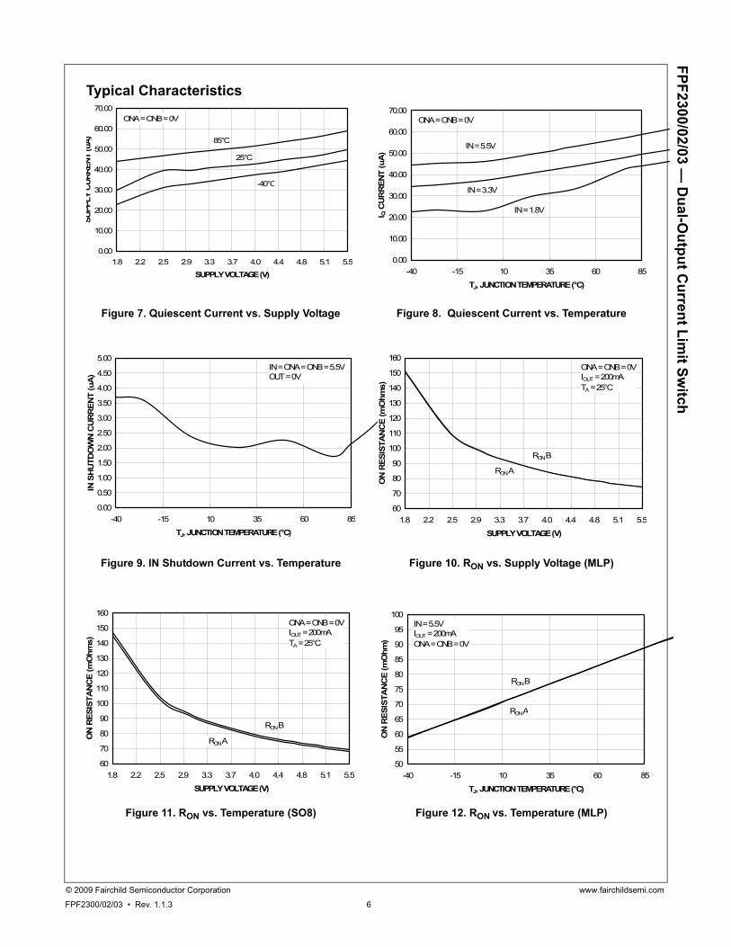
Typical Characteristics
0.00
10.00
20.00
30.00
40.00
50.00
60.00
70.00
1.8 2.2 2.5 2.9 3.3 3.7 4.0 4.4 4.8 5.1 5.5
SUPPLY VOLTAGE (V)
SUPP
LY C
UR
REN
T (u
A)
ONA = ONB = 0V
25°C
85°C
-40°C
0.00
0.50
1.00
1.50
2.00
2.50
3.00
3.50
4.00
4.50
5.00
-40 -15 10 35 60 85
TJ, JUNCTION TEMPERATURE (°C)
IN S
HU
TDO
WN
CU
RR
ENT
(uA
)
IN = ONA = ONB = 5.5VOUT = 0V
60
70
80
90
100
110
120
130
140
150
160
1.8 2.2 2.5 2.9 3.3 3.7 4.0 4.4 4.8 5.1 5.5
SUPPLY VOLTAGE (V)
ON
RES
ISTA
NC
E (m
Ohm
s)
RON A
RON B
ONA = ONB = 0VIOUT = 200mATA = 25°C
Figure 10. RON vs. Supply Voltage (MLP)
Figure 11. RON vs. Temperature (SO8) Figure 12. RON vs. Temperature (MLP)
Figure 9. IN Shutdown Current vs. Temperature
Figure 7. Quiescent Current vs. Supply Voltage Figure 8. Quiescent Current vs. Temperature
0.00
10.00
20.00
30.00
40.00
50.00
60.00
70.00
-40 -15 10 35 60 85
TJ, JUNCTION TEMPERATURE (°C)
I Q C
UR
REN
T (u
A)
IN = 3.3V
IN = 5.5V
IN = 1.8V
ONA = ONB = 0V
60
70
80
90
100
110
120
130
140
150
160
1.8 2.2 2.5 2.9 3.3 3.7 4.0 4.4 4.8 5.1 5.5
SUPPLY VOLTAGE (V)
ON
RES
ISTA
NC
E (m
Ohm
s)
RON A
RON B
ONA = ONB = 0VIOUT = 200mATA = 25°C
50
55
60
65
70
75
80
85
90
95
100
-40 -15 10 35 60 85
TJ, JUNCTION TEMPERATURE (°C)
ON
RES
ISTA
NC
E (m
Ohm
)
RON A
RON B
IN = 5.5VIOUT = 200mAONA = ONB = 0V

FPF2300/02/03 D
ual-Output C
urrent Limit Sw
itch
© 2009 Fairchild Semiconductor Corporation www.fairchildsemi.com
FPF2300/02/03 Rev. 1.1.3 7
Typical Characteristics
50
55
60
65
70
75
80
85
90
-40 -15 10 35 60 85
TJ, JUNCTION TEMPERATURE (°C)
ON
RES
ISTA
NC
E (m
Ohm
)
RON A
RON B
IN = 5.5VIOUT = 200mAONA = ONB = 0V
Figure 16. ON Low Voltage vs. Temperature
Figure 17. Current Limit vs. Supply Voltage Figure 18. Current Limit vs. Temperature
Figure 15. ON High Voltage vs. Temperature
Figure 13. RON vs. Temperature (SO8) Figure 14. ON Threshold Voltage vs. Supply Voltage
0.0
0.3
0.5
0.8
1.0
1.3
1.5
1.8 2.2 2.5 2.9 3.3 3.7 4.0 4.4 4.8 5.1 5.5
SUPPLY VOLTAGE (V)
ON
TH
RES
HO
LD V
OLT
AG
E (V
)
VIH
VIL
TA = 25°C
0.0
0.2
0.4
0.6
0.8
1.0
1.2
-40 -15 10 35 60 85
TJ, JUNCTION TEMPERATURE (°C)
ON
TH
RES
HO
LD V
OLT
AG
E (V
)
IN = 3.3V
IN = 5.5V
IN = 1.8V
0.0
0.2
0.4
0.6
0.8
1.0
1.2
-40 -15 10 35 60 85
TJ, JUNCTION TEMPERATURE (°C)
ON
TH
RES
HO
LD V
OLT
AG
E (V
)
IN = 3.3V
IN = 5.5V
IN = 1.8V
1250
1260
1270
1280
1290
1300
1310
1320
1330
1340
1350
1.8 2.2 2.5 2.9 3.3 3.7 4.0 4.4 4.8 5.1 5.5
SUPPLY VOLTAGE (V)
CU
RR
ENT
LIM
IT (m
A)
ILIM(Typ)A
TA = 25°C
ILIM(Typ)B
1250
1260
1270
1280
1290
1300
1310
1320
1330
1340
1350
-40 -15 10 35 60 85
TJ, JUNCTION TEMPERATURE (°C)
CU
RR
ENT
LIM
IT (m
A)
IN = 3.3VOUTA = OUTB = 3VONA = ONB = 0V
ILIM(Typ)A
ILIM(Typ)B

FPF2300/02/03 D
ual-Output C
urrent Limit Sw
itch
© 2009 Fairchild Semiconductor Corporation www.fairchildsemi.com
FPF2300/02/03 Rev. 1.1.3 8
Typical Characteristics
1
10
100
1000
-40 -15 10 35 60 85
TJ, JUNCTION TEMPERATURE (°C)
TUR
N O
N/O
FF D
ELA
Y TI
ME
(us)
tDOFF
tDON
IN = 3.3VRL = 500 OhmsCL = 0.1 uF
IN = 3.3VRL = 500 Ohms
OUT2V/DIV
IN = 5VON = 3.3VCOUT = 0.1μFRL = 500Ω
ON2V/DIV
IN2V/DIV
200μs/DIV
Figure 23. tRSTRT vs. Temperature Figure 24. tON Response
Figure 22. tRSTRT_BLANK vs. TemperatureFigure 21. tBLANK vs. Temperature
Figure 19. tDON / tDOFF vs. Temperature Figure 20. tRISE / tFALL vs. Temperature
0
2
4
6
8
10
12
14
16
18
20
-40 -15 10 35 60 85
TJ, JUNCTION TEMPERATURE (°C)
RIS
E/FA
LL T
IME
(us)
tF
tR
IN = 3.3VRL = 500 OhmsCL = 0.1 uF
IN = 3.3VRL = 500 Ohms
7.0
7.5
8.0
8.5
9.0
9.5
10.0
10.5
11.0
-40 -15 10 35 60 85
TJ, JUNCTION TEMPERATURE (°C)
OVE
R C
UR
REN
T B
LAN
KIN
G T
IME
(ms)
FLAGB(A)
FLAGB(B)
FPF2300/2IN = 3.3VONA = ONB = 0V
7.0
7.5
8.0
8.5
9.0
9.5
10.0
-40 -15 10 35 60 85
TJ, JUNCTION TEMPERATURE (°C)
STA
RTU
P FL
AG
B B
LAN
KIN
G T
IME
(ms)
FLAGB(A)
FLAGB(B)
FPF2303IN = 3.3VONA = ONB = 0V
500.0
520.0
540.0
560.0
580.0
600.0
620.0
-40 -15 10 35 60 85
TJ, JUNCTION TEMPERATURE (°C)
RES
TAR
T TI
ME
(ms)
OUTA
OUTB
FPF2300IN = 3.3VONA = ONB = 0V

FPF2300/02/03 D
ual-Output C
urrent Limit Sw
itch
© 2009 Fairchild Semiconductor Corporation www.fairchildsemi.com
FPF2300/02/03 Rev. 1.1.3 9
Typical Characteristics
OUT2V/DIV
IN = 5VON = 3.3VCOUT = 0.1μFRL = 500Ω
ON2V/DIV
IN2V/DIV
200μs/DIV
IN = 5VON = 3.3VRL = 5Ω
IN5V/DIV
ON5V/DIV
200μs/DIV
IOUT1A/DIV
COUT = 47μF
COUT = 100μF
COUT = 220μF
COUT = 470μF
Figure 29. Current Limit at Startup with Different Output Capacitor
Figure 30. Output Voltage at Startup with Different Output Capacitor
Figure 27. Startup FLAGB Blanking Time (FPF2303)
Figure 25. tOFF Response Figure 26. Over-Current Blanking Time (FPF2300/2)
Figure 28. Auto-Restart Time (FPF2300)
2ms/DIV
OUT5V/DIV
IN = 5VCOUT = 10μFRL = 2.8ΩON
2V/DIV
FLAGB2V/DIV
IOUT1A/DIV
tBLANK
2ms/DIV
OUT2V/DIV
COUT = 10μFRL = 3.3ΩON
2V/DIV
FLAGB2V/DIV
IOUT1A/DIV
tSTART_BLANK
100ms/DIV
OUT5V/DIV
IN = 5VCOUT = 10μFRL = 2.8Ω
ON2V/DIV
FLAGB2V/DIV
IOUT1A/DIV
tRSTRT
IN = 5VON = 3.3VRL = 5Ω
IN5V/DIV
ON5V/DIV
200μs/DIV
OUT5V/DIV
COUT = 47μF COUT = 220μFCOUT = 100μF COUT = 470μF

FPF2300/02/03 D
ual-Output C
urrent Limit Sw
itch
© 2009 Fairchild Semiconductor Corporation www.fairchildsemi.com
FPF2300/02/03 Rev. 1.1.3 10
Typical Characteristics
OUTB2V/DIV
IN = 5VON = 3.3VCOUTA = 100μF COUTB = 100μFRLA = RLB = 1Ω
IN5V/DIV
ON2V/DIV
400μs/DIV
OUTA2V/DIV
Figure 33. Inrush Response During Capacitive Load Hot Plug-In Event
Figure 31. Current Limit Response Time Both Channels are in OC
Figure 32. Startup FLAGB Blanking Time
Figure 34. Inrush Response During Capacitive and Resistive Load Hot Plug-In Event
FLAGB(B)2V/DIV
IN = 5VON = 3.3VCOUTA = 100μF COUTB = 100μFRLA = RLB = 1Ω
IN5V/DIV
ON2V/DIV
10ms/DIV
FLAGB(A)2V/DIV
OUT5V/DIV
IN = 5VCOUT = 47μFCL = 470μFRL = 5Ω
IN5V/DIV
ON5V/DIV
1ms/DIV
IOUT500mA/DIV
OUT5V/DIV
IN = 5VCIN = 10μFCOUT = 100μFCL = 47μF
IN5V/DIV
ON5V/DIV
200μs/DIV
IOUT2A/DIV

© 2009 Fairchild Semiconductor Corporation www.fairchildsemi.com
FPF2300/02/03 Rev. 1.1.3 11
FPF2300/02/03 D
ual-Output C
urrent Limit Sw
itch
Description of OperationThe FPF2300, FPF2302, and FPF2303 are dual-output current-limit switches designed to meet notebook computer, peripheralUSB port, and point-of-load (POL) application power requirements.Dual-output current can be used where dual or quad USB ports arepowered by hosts or self-powered hubs. The FPF230X familyoffers control and protection while providing optimum operationcurrent for a safe design practice. The core of each switch is atypical 75mΩ (IN = 5.5V) P-channel MOSFET and a controllercapable of functioning over an input operating range of 1.8-5.5V.The FPF230X family offers current limiting, UVLO (under-voltagelockout), and thermal shutdown protection per each switch. In theevent of an over-current condition, the load switch limits the load tocurrent limit value. The minimum current limit is set to 1100mA.
On/Off ControlThe ON pin is active LOW for FPF2300/2/3 and controls the stateof the switch. Pulling the ON pin continuous to LOW holds theswitch in the ON state. The switch moves into the OFF state whenthe ON pin is pulled HIGH or if a fault is encountered. For allversions, an under-voltage on input voltage or a junctiontemperature in excess of 140°C overrides the ON control to turn offthe switch. In addition, excessive currents cause the switch to turnoff in the FPF2300 and FPF2302 after a 10ms blanking time. TheFPF2300 has an auto-restart feature that automatically turns theswitch ON again after 504ms. For the FPF2302, the ON pin mustbe toggled to turn on the switch again. The FPF2303 does not turnoff in response to an over-current condition, but remains operatingin a constant-current mode as long as ON is enabled and thethermal shutdown or UVLO is not activated. The ON pin does nothave a pull-down or pull-up resistor and should not be left floating.
Current LimitingThe current limit ensures that the current through the switchdoesn't exceed a maximum value, while not limiting at less than aminimum value. FPF230X family has dual-output load switchesbeing housed in one package. The minimum current at which bothswitches start limiting the load current is set to 1100mA. TheFPF2300 and FPF2302 have a blanking time of 10ms (typical),during which the switch acts as a constant current source. At theend of the blanking time, the switch is turned off. The FPF2303 hasno current limit blanking period, so it remains in a constant currentstate until the ON pin of the affected switch is deactivated or thethermal shutdown turns off the switch.
Fault ReportingOver-current, input under-voltage, and over-temperature faultconditions are signaled out by the FLAGB pin going LOW. A UVLOfault is reported on both FLAGB(A) and FLAGB(B) simultaneously,while over-current and over-temperature condition faults arereported independently. FPF2300 and FPF2302 have a currentfault blanking feature that prevents over-current faults shorter thanthe blanking time (tBLANK(Typ) = 10ms) from triggering the faultsignal (FLAGB) output.If the over-current condition persists beyond the blanking time, theFPF2300 pulls the FLAGB pin LOW and shuts the switch off. If theON pin is kept active, an auto-restart feature releases the FLAGBpin and turns the switch on again after a 504ms auto-restart time(tRSTRT). If the over-current condition persists beyond the blankingtime, the FPF2302 has a latch-off feature that pulls the FLAGB pinLOW and shuts the switch off. The switch is kept off and theFLAGB pin kept LOW until the ON pin is toggled. The FPF2303responds to an overload condition by immediately pulling theFLAGB pin LOW and the switch remains in constant current modeuntil the output overload condition is removed. The FPF2303 has a
startup blanking feature that prevents current faults related to star-tup transients from triggering the FLAGB output. The startup blank-ing feature is effective for the first 10ms (typical) following deviceturn-on via ON pin.
The FLAGB outputs are two open-drain MOSFETs that require apull-up resistor on each FLAGB pin. FLAGB can be pulled HIGH toa voltage source other than input supply with maximum 5.5V. A100KΩ pull-up resistor is recommended. When the ON pin is inac-tive, the FLAGB is disabled to reduce current draw from the supply.If the FLAGB is not used, the FLAGB can be connected to groundon the PCB.
.
device wakeup
device wakeup
ON
IN
FLAGB
OUT
ILOAD
ILIMIT
10% VOUT
90% VOUT
RISE TIME
VIN
ON
FLAGB
RL*VOUT
tBLANK
ILOAD
ILIMIT
tRSTRT
Over current condtion
ILMIT
Figure 35. FLAGB Assertion in Under-Voltage Fault
Figure 36. FPF2300 FLAGB Reports While Entering into an Over-Current Condition
Note: 6. An over-current condition signal loads the output with a
heavy load current larger than ILIM value.

© 2009 Fairchild Semiconductor Corporation www.fairchildsemi.com
FPF2300/02/03 Rev. 1.1.3 12
FPF2300/02/03 D
ual-Output C
urrent Limit Sw
itch
Figure 37. FPF2300 FLAGB While and Over-Current Condition is Applied
Note: 7. An over-current condition signal loads the output with a
heavy load current larger than ILIMIT value.
Under-Voltage Lockout (UVLO)The under-voltage lockout feature turns off the switch if theinput voltage drops below the under-voltage lockout threshold.With the ON pin active (ON pin pulled LOW), the input voltagerising above the under-voltage lockout threshold causes acontrolled turn-on of the switch and limits current overshoot. If adevice is in UVLO condition, both FLAGBs go LOW and indicatethe fault condition. The device detects the UVLO condition wheninput voltage goes below UVLO voltage, but remains above1.3V (typical).
Reverse Current BlockingEach switch of FPF2300/2/3 has an independent reversecurrent blocking feature that protects input source againstcurrent flow from output to input. For a standard USB powerdesign, this is an important feature that protects the USB hostfrom being damaged due to reverse current flow on VBUS. Toactivate the reverse current blocking, the switch must be in OFFstate (ON pins inactivated) so that no current flows from theoutput to the input. The FLAGB operation is independent of thereverse current blocking and does not report a fault condition ifthis feature is activated.
Thermal ShutdownThe thermal shutdown protects the device from internally orexternally generated excessive temperatures. Each switch hasan individual thermal shutdown protection function and operatesindependently as adjacent switch temperatures increase above140°C. If one switch is in normal operation and shutdownprotection of second switch is activated, the first channelcontinues to operate if the affected channel's heat staysconfined. The over-temperature in one channel can shut downboth switches due to rapidly generated excessive load currentsresulting in very high power dissipation. Generally, a thermallyimproved board layout can provide heat sinking and allow heatto stay confined and not affect the second switch operation.
During an over-temperature condition, the FLAGB is pulledLOW and the affected switch is turned off. If the temperature ofthe die drops below the threshold temperature, the switch
automatically turns on again. To avoid unwanted thermaloscillations, a 10°C (typical) thermal hysteresis is implementedbetween thermal shutdown entry and exit temperatures.
If output of both switches are connected together and anexcessive load current activates thermal protection of both, thecontroller can shut down the switches after both FLAGB outputsgo LOW and turn on both channels again. This providessimultaneous switch turn on. Thermal protection is for deviceprotection and should not be used as regular operation.
Input CapacitorTo limit the voltage drop on the input supply caused by transientinrush currents when the switch is turned on into dischargedload capacitors or a short-circuit; an input capacitor, CIN, isrecommended between IN and GND. The FPF2310/2/3/3Lfeatures a fast current limit response time of 20μs. An inrushcurrent (also known as surge current) could occur during thecurrent limit response time while the switch is responding to anover-current condition caused by large output capacitors. A10μF ceramic capacitor, CIN, is required to provide charges forthe inrush current and prevent input voltage drop at turn on.Higher values of CIN can be used to further reduce voltage drop.
Output CapacitorA 0.1μF to 1μF capacitor, COUT, should be placed between theOUT and GND pins. This capacitor prevents parasitic boardinductances from forcing output voltage below GND when theswitch turns off. This capacitor should have a low dissipationfactor. An X7R MLCC (Multilayer Ceramic Chip) capacitors isrecommended.
For the FPF2300 and FPF2302, the total output capacitanceneeds to be kept below a maximum value, COUT(MAX), toprevent the part from registering an over-current conditionbeyond the blanking time and shutdown. The maximum outputcapacitance for a giving input voltage can be determined fromthe following:
For example, in a 5V application, COUT(MAX) can be determinedas:
VIN
ON
FLAGB
VOUT
Startup tBLANK
ILOADILIMIT
Over current condtion
Thermal Shutdown
Device Cools Off
(1)COUT(MAX) =ILIM(MIN) x tBLANK(MIN)
VIN
(2)COUT(MAX)(IN = 5V) =1.1A x 5ms
5
= 1.1mF

© 2009 Fairchild Semiconductor Corporation www.fairchildsemi.com
FPF2300/02/03 Rev. 1.1.3 13
FPF2300/02/03 D
ual-Output C
urrent Limit Sw
itch
Application Information
Figure 38. Self Powered 4-Port USB Hub Using a Single FPF230XFPF230X is designed to simplify USB port power design basedon self-powering USB host/hub applications. A self-poweringUSB port is powered by a local 5V power supply, not by anupstream port. Each port should supply at least 500mA to eachdownstream function based on USB 2.0 specification. Imple-mentation can depend on the number of USB ports and current
capability per port required in actual power designs. FPF230Xhas 1.1A minimum current limit per output, which can cover twoports, as shown in Figure 38. Four USB ports can be imple-mented with a single FPF230X part and current limiting is pro-vided based on a two-port basis for a cost-effective solution.
Figure 39. Individual Port Power Management for Self-Powered 4-Port USB Hub In Figure 39, each USB port is connected with each output.Four USB ports can be implemented with two FPF230X parts.Current limiting and control are provided based on a single port.
Current capability per port has more headroom; up to a mini-mum of 1.1A per port.
OFF ON ONA
IN
GND
FPF2300/2/3FLAGB(B)
OUTA
FLAGB(A)
OFF ON ONB OUTB
Host5V
DownstreamUSB Port
DownstreamUSB Port
DownstreamUSB Port
DownstreamUSB Port
1μF
33μF
33μF
33μF
33μF
10KΩ
10KΩ
OFF ON ONA
IN
GND
FPF2300/2/3FLAGB(B)
OUTA
FLAGB(A)
OFF ON ONB OUTB
Host5V
DownstreamUSB Port
DownstreamUSB Port
1μF
33μF
33μF
10KΩ
10KΩ
OFF ON ONA
IN
GND
FPF2300/2/3FLAGB(B)
OUTA
FLAGB(A)
OFF ON ONB OUTB
DownstreamUSB Port
DownstreamUSB Port
1μF
33μF
33μF
10KΩ
10KΩ

© 2009 Fairchild Semiconductor Corporation www.fairchildsemi.com
FPF2300/02/03 Rev. 1.1.3 14
FPF2300/02/03 D
ual-Output C
urrent Limit Sw
itch
Figure 40. Self-Powered USB Port for High Current DemandHigh current, over 2A, is sometimes required to supply enoughpower to downstream functions. As shown in Figure 40, a 2.2A
minimum load current can be achieved by tying dual outputstogether.
Power DissipationDuring normal operation as a switch, the power dissipation ofthe device is small and has little effect on the operatingtemperature of the part. The maximum power dissipation forboth switches while the switch is in normal operation occurs justbefore both channels enter into current limit. This may becalculated using the formula:
For example, for a 5V application, maximum normal operationpower loss while both switches delivering output current up to1.1A, can be calculated as:
The maximum junction temperature should be limited to 125°Cunder normal operation. Junction temperature can be calcu-lated using the formula below:
where:
TJ is junction temperature;PD is power dissipation across the switch;RθJA is thermal resistance junction to ambient of the package;TA is ambient temperature.
For the example, TJ(MAX)(Normal operation) for an SO8 packagewith TA=25°C while both switches are delivering up to 1.1A iscalculated as:
If the part goes into current limit, the maximum powerdissipation occurs when the output of switch is shorted toground. For the FPF2300 the power dissipation scales with theauto-restart time, tRSTRT, and the over-current blanking time,tBLANK. In this case, the maximum power dissipated for theFPF2300 is::
which results in:
Note that this is below the maximum package power dissipationand the thermal shutdown feature protection provides additionalsafety to protect the part from damage due to excessiveheating. The junction temperature is only able to increase to thethermal shutdown threshold. Once this temperature has beenreached, toggling ON has no affect until the junctiontemperature drops below the thermal shutdown exittemperature. For the FPF2303, a short on both outputs causesboth switches to operate in a constant current state anddissipate a worst-case power of:
As both FPF2303 outputs are connected to GND.
This power dissipation is significant and activates both thermalshutdown blocks and the part can cycle in and out of thermalshutdown as long as the ON pin is activated (pulled LOW) andthe output short is present.
OFF ON ONA
IN
GND
FPF2300/2/3FLAGB(B)
OUTA
FLAGB(A)
OFF ON ONB OUTB
Host5V
DownstreamUSB Port
1μF
33μF
10KΩ
10KΩ
PD_MAX(Normal Operation) = 2 x (ILIM(MIN))2 x RON(MAX) (3)
PD_MAX(Normal Operation)(IN = 5V) = 2 x (1.1)2 x 0.14
= 338mW
(4)
TJ = PD x RθJA + TA (5)
TJ(MAX)(NormalOperation)
= PD_MAX(Normal Operation)(IN = 5V) x 125 + 25
= 78.4°C
(6)
PD_MAX(CurrentLimit) =tBLANK
tBLANK + tRSTRT2 x x IN(MAX) x ILIM(MAX)
(7)
PD_MAX(CurrentLimit) = 10
10 + 5042 x (8)x 5.5 x 1.5 = 321mW
(9)PMAX = 2 x IN(MAX) x ILIM(MAX) = 2 x 5.5 x1.5 = 16.5 W

© 2009 Fairchild Semiconductor Corporation www.fairchildsemi.com
FPF2300/02/03 Rev. 1.1.3 15
FPF2300/02/03 D
ual-Output C
urrent Limit Sw
itch
PCB Layout RecommendationsFor the best performance, all traces should be as short aspossible. To be most effective, the input and output capacitorsshould be placed close to the device to minimize the effects thatparasitic trace inductances may have on normal and short-circuit operation. Using wide traces for IN, OUTs, and GND pinshelps minimize parasitic electrical effects and the case-to-ambient thermal impedance.
Improving Thermal PerformanceImproper layout could result in higher junction temperature andtriggering the thermal shutdown protection feature. This concernis particularly significant for the FPF2303, where both channelsoperate in constant current mode in the overload conditions andduring fault condition the outputs are shorted, resulting in largevoltage drop across switches. In this case, power dissipation ofthe switch (PD = (VIN - VOUT) x ILIM(MAX)) could exceed themaximum absolute power dissipation of part.
The following techniques improve the thermal performance ofthis family of devices. These techniques are listed in order ofthe significance of impact.
1. Thermal performance of the load switch can be improvedby connecting the DAP (Die Attach Pad) of MLP 3x3mmpackage to the GND plane of the PCB.
2. Embedding two exposed through-hole vias into the DAP(pin 9) provides a path for heat to transfer to the back GNDplane of the PCB. A drill size of round, 15 mils (0.4mm),with 1-ounce copper plating is recommended to createappropriate solder reflow. A smaller size hole prevents thesolder from penetrating into the via, resulting in device lift-up. Similarly, a larger via hole consumes excessive solderand may result in voiding of the DAP.
Figure 41. Two Through-Hole Open Vias Embedded in DAP
3. The IN, OUTs, and GND pins dissipate most of the heatgenerated during a high load current condition. Figure 42illustrates a proper layout for devices in MLP 3x3mmpackages. IN, OUTs, and GND pins are connected toadequate copper so heat may be transferred as efficientlyas possible out of the device. The low-power FLAGB andON pin traces may be laid out diagonally from the device tomaximize the area available to the ground pad. Placing theinput and output capacitors as close to the device aspossible also contributes to heat dissipation, particularlyduring high load currents.
Figure 42. Proper Layout of Output and Ground Copper Area
15mil
25mil

© 2009 Fairchild Semiconductor Corporation www.fairchildsemi.com
FPF2300/02/03 Rev. 1.1.3 16
FPF2300/02/03 D
ual-Output C
urrent Limit Sw
itch
FPF230X Evaluation BoardThe FPF230X evaluation board has components and circuitry todemonstrate FPF2300/2/3 load switch functions and features,accommodating both the MLP 3x3mm and SO8 packages. Thestate of the each channel can be configured using J1 and J2jumpers. In addition, both channels can be controlled by ONAand ONB test pints. Thermal performance of the board isimproved using techniques in the layout recommendationssection. R3 and R4 resistors are used on the board to sink alight load current when switches are activated.
Figure 43. Top, SST and AST Layers (MLP 3x3mm and SO8)
Figure 44. Bottom and ASB Layers
Figure 45. Zoom-In to Top Layer
Releated ResourcesFPF2300/02/03 Evaluation Board User Guide; Power Switch for USB Applications


NOTES:
A. CONFORMS TO JEDEC REGISTRATION MO-229,
VARIATION VEEC, DATED 11/2001.
B. DIMENSIONS ARE IN MILLIMETERS.
C. DIMENSIONS AND TOLERANCES PER
ASME Y14.5M, 2009.
D. LAND PATTERN RECOMMENDATION IS
EXISTING INDUSTRY LAND PATTERN.
E. DRAWING FILENAME: MKT-MLP08Drev3
0.10 C A B
0.05 C
TOP VIEW
BOTTOM VIEW
RECOMMENDED LAND PATTERN
0.10 C
0.08 C
3.00
3.00
0.10 C
2X
2X
SEATING
PLANE
0.10 C
(0.20)
1.99
3.30
(0.65)
1
4
58
5
8
4
1
0.65
1.95
0.65 TYP
2.37
1.42
0.42 TYP
PIN #1 IDENT
A
B
0.80 MAX
0.05
0.00
C
FRONT VIEW
2.25MAX
PIN #1 IDENT
1.30MAX
0.45
0.20
0.25
0.35

www.onsemi.com1
ON Semiconductor and are trademarks of Semiconductor Components Industries, LLC dba ON Semiconductor or its subsidiaries in the United States and/or other countries.ON Semiconductor owns the rights to a number of patents, trademarks, copyrights, trade secrets, and other intellectual property. A listing of ON Semiconductor’s product/patentcoverage may be accessed at www.onsemi.com/site/pdf/Patent−Marking.pdf. ON Semiconductor reserves the right to make changes without further notice to any products herein.ON Semiconductor makes no warranty, representation or guarantee regarding the suitability of its products for any particular purpose, nor does ON Semiconductor assume any liabilityarising out of the application or use of any product or circuit, and specifically disclaims any and all liability, including without limitation special, consequential or incidental damages.Buyer is responsible for its products and applications using ON Semiconductor products, including compliance with all laws, regulations and safety requirements or standards,regardless of any support or applications information provided by ON Semiconductor. “Typical” parameters which may be provided in ON Semiconductor data sheets and/orspecifications can and do vary in different applications and actual performance may vary over time. All operating parameters, including “Typicals” must be validated for each customerapplication by customer’s technical experts. ON Semiconductor does not convey any license under its patent rights nor the rights of others. ON Semiconductor products are notdesigned, intended, or authorized for use as a critical component in life support systems or any FDA Class 3 medical devices or medical devices with a same or similar classificationin a foreign jurisdiction or any devices intended for implantation in the human body. Should Buyer purchase or use ON Semiconductor products for any such unintended or unauthorizedapplication, Buyer shall indemnify and hold ON Semiconductor and its officers, employees, subsidiaries, affiliates, and distributors harmless against all claims, costs, damages, andexpenses, and reasonable attorney fees arising out of, directly or indirectly, any claim of personal injury or death associated with such unintended or unauthorized use, even if suchclaim alleges that ON Semiconductor was negligent regarding the design or manufacture of the part. ON Semiconductor is an Equal Opportunity/Affirmative Action Employer. Thisliterature is subject to all applicable copyright laws and is not for resale in any manner.
PUBLICATION ORDERING INFORMATIONN. American Technical Support: 800−282−9855 Toll FreeUSA/Canada
Europe, Middle East and Africa Technical Support:Phone: 421 33 790 2910
Japan Customer Focus CenterPhone: 81−3−5817−1050
www.onsemi.com
LITERATURE FULFILLMENT:Literature Distribution Center for ON Semiconductor19521 E. 32nd Pkwy, Aurora, Colorado 80011 USAPhone: 303−675−2175 or 800−344−3860 Toll Free USA/CanadaFax: 303−675−2176 or 800−344−3867 Toll Free USA/CanadaEmail: [email protected]
ON Semiconductor Website: www.onsemi.com
Order Literature: http://www.onsemi.com/orderlit
For additional information, please contact your localSales Representative
© Semiconductor Components Industries, LLC
Related Documents


![Konstytucja - Frysztaksp.frysztak.pl/pliki/uploads/2014/05/panaceumczerwiec2016.pdf · Panaceum 4 Konstytucja 3 maja t ] lîõXìñXîìíò Xv µo] Ìl}ov i} Çs ]' akademia ku czci](https://static.cupdf.com/doc/110x72/5e3db0362e9baa288f253f16/konstytucja-panaceum-4-konstytucja-3-maja-t-lxx-xv-o-oelov.jpg)

![2019ÂÈ ³¡3°O´ôÂȵsà ²·file.megastudy.net/FileServer/UNI_HWP/non_file/19juyo/Y... · 2017-12-01 · 2019ÂÈ ³¡3°O´ôÂȵsà ²· # [® ´'¼ Àë° ] 2017.3 ( )´ôÂÈÀo](https://static.cupdf.com/doc/110x72/5ed49a3040206955426985d4/2019-3osf-file-2017-12-01-2019-3osf.jpg)
