TABLE I. PHYSICAL PARAMETERS OF THE CMUT CELLS t m (µm) f r (kHz) a (mm) t g (µm) t i (µm) A 380 84.9 4 4-4.5 0.5 B 380 54.8 5 4-4.5 0.5 C 380 38.2 6 4-4.5 0.5 Wafer Bonded Capacitive Micromachined Underwater Transducers Selim Olcum, 1,* Kagan Oğuz, 1 Muhammed N. Şenlik, 1 F. Yalçın Yamaner, 2 Ayhan Bozkurt, 2 Abdullah Atalar, 1 Hayrettin Köymen, 1 1 Bilkent University, Electrical & Electronics Engineering Department, Ankara, 06800 TURKEY 2 Sabancı University, Faculty of Engineering & Natural Sciences, İstanbul, 34956 TURKEY * [email protected] Abstract — In this work we have designed, fabricated and tested CMUTs as underwater transducers. Single CMUT membranes with three different radii and 380 microns of thickness are fabricated for the demonstration of an underwater CMUT element. The active area of the transducer is fabricated on top of a 3″ silicon wafer. The silicon wafer is bonded to a gold electrode coated glass substrate wafer 10 cm in diameter. Thermally grown silicon oxide layer is used as the insulation layer between membrane and substrate electrodes. Electrical contacts and insulation are made by epoxy layers. Single CMUT elements are tested in air and in water. Approximately 40% bandwidth is achieved around 25 KHz with a single underwater CMUT cell. Radiated pressure field due to second harmonic generation when the CMUTs are driven with high sinusoidal voltages is measured. Keywords-component; Capacitive Micromachined Ultrasonic Transducers, underwater transducers, anodic bonding, second harmonic generation. I. I NTRODUCTION Capacitive micromachined ultrasonic transducers (CMUT) have been under investigation for almost 15 years. Many fabrication technologies are proposed based on sacrificial layer process or wafe r bonding process in order to fabricate effic ient ultrasonic transducers. Applications such as medical imaging, high intensity focussed ultrasound, intravascular ultrasound, airborne acoustics, microphones and nondestructive evaluation attracted attention for possible use of CMUTs. The operational frequency range in focus has been mainly between 1 MHz to 30 MHz. Recently, potential of achieveing a large bandwidth and high efficiency from CMUTs attracted more applications at lower frequency bands. Recent studies show that airborne CMUTs can achieve a high transduction efficiency and bandwidth around 50 KHz [ 1]. Acoustical energy has been used underwater in several areas ranging from commercial, scientific and military areas. In lower frequency range (1 kHz – 100 kHz), acoustical systems are utilized underwater and on surface platform applications, i.e., navigation systems, active and passive sonar transducers, seismic and environmental observation systems. In the higher frequency range the applications are more limited due to the higher attenuation and noise underwater. Such applications are restricted in short ranges. Most common practices are purse seining, Doppler sonars and underwater imaging systems. Achieving a high acoustical power during the transmit cycle and a high sensitivity during the receive cycle in a large bandwidth is difficult. In the case of building an array of transducers, building transmit and receive elements along with the required interconnects to the dedicated transmit and receive circuitry is another challenge. For low frequency applications production of thin tr ansducers is also a difficult task. It’s been demonstrated that CMUTs offer excellent properti es such as wi de bandwid th [2], ease of array f abricatio n and integrating the dedicated electronics along with the transducers, [3] thanks to the microfabrication techniques utilized during fabrication. Recent studies show that high power ou tputs can be o btained [4] and high r eceive sensitivities can be achieved using CMUTs [2]. CMUT’s large bandwidth, high sensitivity, low cost fabrication and ease of integration with electronics make it a good candidate for an underwater transducer. However, extra care should be exercised in order to utilize the full merit of the CMUTs. Especially, nonlinear behavior d uring tran smit mode should be taken into account. In this work we have designed, fabricated and tested CMUTs as underwater transducers. Single CMUT membranes with three different radii and 380 µm of thickness are fabricated for the demonstration of an underwater CMUT cell. The results of the underwater measurements are reported and compared with those obtained from an equivalent circuit model. II. DESIGNING AN UNDERWATER TRANSDUCER In principle, CMUTs work with a fixed DC bias generating a static force deflecting the membrane. Therefore, any external static force changes the operating point of the device. Underwater hydrostatic pressure affects the operation of the CMUT membranes. In this study, we limit ourselves to the This work is supported by TUBITAK under the grants 105E023 and 107T921. 976 978-1-4244-4390-1/09/$25.00 ©2009 IEEE 2009 IEEE International Ultrasonics Symposium Proceedings 10.1109/ULTSYM.2009.0237 Authorized licensed use limited to: Vinay Gupta. Downloaded on August 09,2010 at 10:15:40 UTC from IEEE Xplore. Restrictions apply.

Welcome message from author
This document is posted to help you gain knowledge. Please leave a comment to let me know what you think about it! Share it to your friends and learn new things together.
Transcript
7/31/2019 UW1
http://slidepdf.com/reader/full/uw1 1/4
TABLE I. PHYSICAL PARAMETERS OF THE CMUT CELLS
tm (µm) f r (kHz) a (mm) tg (µm) ti (µm)
A 380 84.9 4 4-4.5 0.5
B 380 54.8 5 4-4.5 0.5
C 380 38.2 6 4-4.5 0.5
Wafer Bonded Capacitive Micromachined
Underwater Transducers
Selim Olcum,1,*
Kagan Oğuz,1
Muhammed N. Şenlik,1
F. Yalçın Yamaner,2
Ayhan Bozkurt,2 Abdullah Atalar,1 Hayrettin Köymen,1
1 Bilkent University, Electrical & Electronics Engineering Department, Ankara, 06800 TURKEY
2 Sabancı University, Faculty of Engineering & Natural Sciences, İstanbul, 34956 TURKEY* [email protected]
Abstract — In this work we have designed, fabricated and tested
CMUTs as underwater transducers. Single CMUT membranes
with three different radii and 380 microns of thickness are
fabricated for the demonstration of an underwater CMUT
element. The active area of the transducer is fabricated on top of
a 3″ silicon wafer. The silicon wafer is bonded to a gold electrode
coated glass substrate wafer 10 cm in diameter. Thermally grown
silicon oxide layer is used as the insulation layer betweenmembrane and substrate electrodes. Electrical contacts and
insulation are made by epoxy layers. Single CMUT elements are
tested in air and in water. Approximately 40% bandwidth is
achieved around 25 KHz with a single underwater CMUT cell.
Radiated pressure field due to second harmonic generation when
the CMUTs are driven with high sinusoidal voltages is measured.
Keywords-component; Capacitive Micromachined Ultrasonic
Transducers, underwater transducers, anodic bonding, second
harmonic generation.
I. I NTRODUCTION
Capacitive micromachined ultrasonic transducers (CMUT)have been under investigation for almost 15 years. Manyfabrication technologies are proposed based on sacrificial layer process or wafer bonding process in order to fabricate efficientultrasonic transducers. Applications such as medical imaging,high intensity focussed ultrasound, intravascular ultrasound,airborne acoustics, microphones and nondestructive evaluationattracted attention for possible use of CMUTs. The operationalfrequency range in focus has been mainly between 1 MHz to30 MHz. Recently, potential of achieveing a large bandwidthand high efficiency from CMUTs attracted more applications atlower frequency bands. Recent studies show that airborneCMUTs can achieve a high transduction efficiency and bandwidth around 50 KHz [1].
Acoustical energy has been used underwater in severalareas ranging from commercial, scientific and military areas. Inlower frequency range (1 kHz – 100 kHz), acoustical systemsare utilized underwater and on surface platform applications,i.e., navigation systems, active and passive sonar transducers,seismic and environmental observation systems. In the higher frequency range the applications are more limited due to thehigher attenuation and noise underwater. Such applications arerestricted in short ranges. Most common practices are purse
seining, Doppler sonars and underwater imaging systems.
Achieving a high acoustical power during the transmitcycle and a high sensitivity during the receive cycle in a large bandwidth is difficult. In the case of building an array of transducers, building transmit and receive elements along withthe required interconnects to the dedicated transmit and receivecircuitry is another challenge. For low frequency applications production of thin transducers is also a difficult task.
It’s been demonstrated that CMUTs offer excellent properties such as wide bandwidth [2], ease of array fabrication
and integrating the dedicated electronics along with thetransducers, [3] thanks to the microfabrication techniquesutilized during fabrication. Recent studies show that high power outputs can be obtained [4] and high receive sensitivitiescan be achieved using CMUTs [2]. CMUT’s large bandwidth,high sensitivity, low cost fabrication and ease of integrationwith electronics make it a good candidate for an underwater transducer. However, extra care should be exercised in order toutilize the full merit of the CMUTs. Especially, nonlinear behavior during transmit mode should be taken into account.
In this work we have designed, fabricated and testedCMUTs as underwater transducers. Single CMUT membraneswith three different radii and 380 µm of thickness are
fabricated for the demonstration of an underwater CMUT cell.The results of the underwater measurements are reported andcompared with those obtained from an equivalent circuitmodel.
II. DESIGNING AN UNDERWATER TRANSDUCER
In principle, CMUTs work with a fixed DC bias generatinga static force deflecting the membrane. Therefore, any externalstatic force changes the operating point of the device.Underwater hydrostatic pressure affects the operation of theCMUT membranes. In this study, we limit ourselves to the
This work is supported by TUBITAK under the grants 105E023 and
107T921.
976978-1-4244-4390-1/09/$25.00 ©2009 IEEE 2009 IEEE International Ultrasonics Symposium Proceedings
10.1109/ULTSYM.2009.0237
Authorized licensed use limited to: Vinay Gupta. Downloaded on August 09,2010 at 10:15:40 UTC from IEEE Xplore. Restrictions apply.
7/31/2019 UW1
http://slidepdf.com/reader/full/uw1 2/4
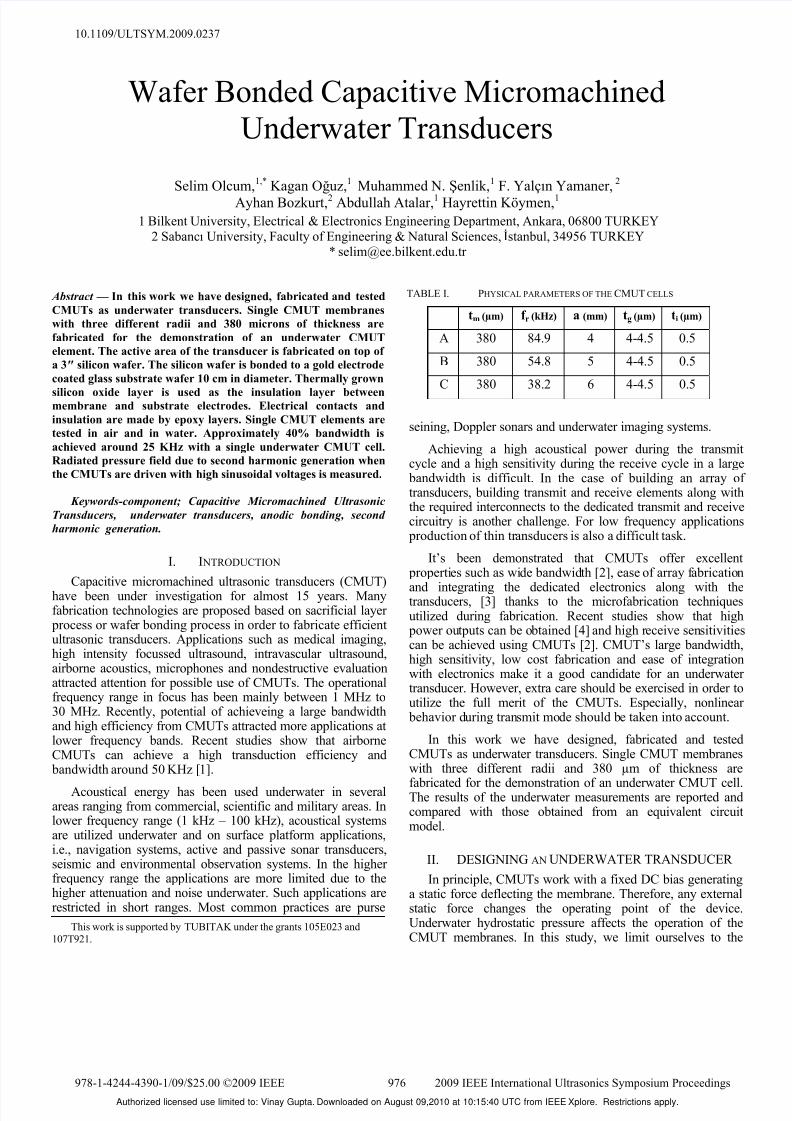
Figure 1. Calculated conductances of cells A, B and C in water for
100 V pp applied with 50 V DC bias. Calculations are made using thee uivalent circuit develo ed in 5 .
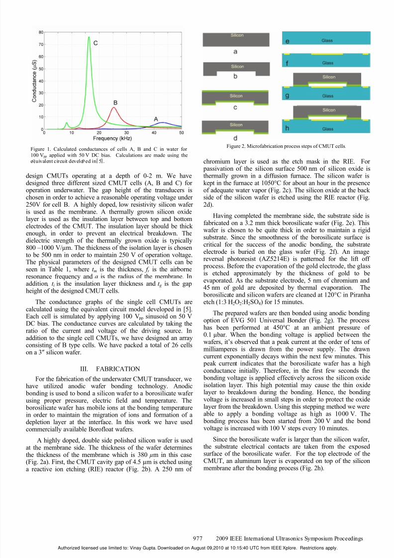
Figure 2. Microfabrication process steps of CMUT cells.
design CMUTs operating at a depth of 0-2 m. We havedesigned three different sized CMUT cells (A, B and C) for operation underwater. The gap height of the transducers is
chosen in order to achieve a reasonable operating voltage under 250V for cell B. A highly doped, low resistivity silicon wafer is used as the membrane. A thermally grown silicon oxidelayer is used as the insulation layer between top and bottomelectrodes of the CMUT. The insulation layer should be thick enough, in order to prevent an electrical breakdown. Thedielectric strength of the thermally grown oxide is typically800 –1000 V/µm. The thickness of the isolation layer is chosento be 500 nm in order to maintain 250 V of operation voltage.The physical parameters of the designed CMUT cells can beseen in Table 1, where t m is the thickness, f r is the airborneresonance frequency and a is the radius of the membrane. Inaddition , t i is the insulation layer thickness and t g is the gap
height of the designed CMUT cells.The conductance graphs of the single cell CMUTs are
calculated using the equivalent circuit model developed in [5].Each cell is simulated by applying 100 V pp sinusoid on 50 VDC bias. The conductance curves are calculated by taking theratio of the current and voltage of the driving source. Inaddition to the single cell CMUTs, we have designed an arrayconsisting of B type cells. We have packed a total of 26 cellson a 3″ silicon wafer.
III. FABRICATION
For the fabrication of the underwater CMUT transducer, wehave utilized anodic wafer bonding technology. Anodic
bonding is used to bond a silicon wafer to a borosilicate wafer using proper pressure, electric field and temperature. The borosilicate wafer has mobile ions at the bonding temperaturein order to maintain the migration of ions and formation of adepletion layer at the interface. In this work we have usedcommercially available Borofloat wafers.
A highly doped, double side polished silicon wafer is usedat the membrane side. The thickness of the wafer determinesthe thickness of the membrane which is 380 µm in this case(Fig. 2a). First, the CMUT cavity gap of 4.5 µm is etched usinga reactive ion etching (RIE) reactor (Fig. 2b). A 250 nm of
chromium layer is used as the etch mask in the RIE. For passivation of the silicon surface 500 nm of silicon oxide isthermally grown in a diffusion furnace. The silicon wafer iskept in the furnace at 1050°C for about an hour in the presenceof adequate water vapor (Fig. 2c). The silicon oxide at the back
side of the silicon wafer is etched using the RIE reactor (Fig.2d).
Having completed the membrane side, the substrate side isfabricated on a 3.2 mm thick borosilicate wafer (Fig. 2e). Thiswafer is chosen to be quite thick in order to maintain a rigidsubstrate. Since the smoothness of the borosilicate surface iscritical for the success of the anodic bonding, the substrateelectrode is buried on the glass wafer (Fig. 2f). An imagereversal photoresist (AZ5214E) is patterned for the lift off process. Before the evaporation of the gold electrode, the glassis etched approximately by the thickness of gold to beevaporated. As the substrate electrode, 5 nm of chromium and45 nm of gold are deposited by thermal evaporation. The
borosilicate and silicon wafers are cleaned at 120°C in Piranhaetch (1:3 H2O2:H2SO4) for 15 minutes.
The prepared wafers are then bonded using anodic bondingoption of EVG 501 Universal Bonder (Fig. 2g). The processhas been performed at 450°C at an ambient pressure of 0.1 µbar. When the bonding voltage is applied between thewafers, it’s observed that a peak current at the order of tens of milliamperes is drawn from the power supply. The drawncurrent exponentially decays within the next few minutes. This peak current indicates that the borosilicate wafer has a highconductance initially. Therefore, in the first few seconds the bonding voltage is applied effectively across the silicon oxideisolation layer. This high potential may cause the thin oxide
layer to breakdown during the bonding. Hence, the bondingvoltage is increased in small steps in order to protect the oxidelayer from the breakdown. Using this stepping method we wereable to apply a bonding voltage as high as 1000 V. The bonding process has been started from 200 V and the bondvoltage is increased with 100 V steps every 10 minutes.
Since the borosilicate wafer is larger than the silicon wafer,the substrate electrical contacts are taken from the exposedsurface of the borosilicate wafer. For the top electrode of theCMUT, an aluminum layer is evaporated on top of the siliconmembrane after the bonding process (Fig. 2h).
977 2009 IEEE International Ultrasonics Symposium Proceedings
Authorized licensed use limited to: Vinay Gupta. Downloaded on August 09,2010 at 10:15:40 UTC from IEEE Xplore. Restrictions apply.
7/31/2019 UW1
http://slidepdf.com/reader/full/uw1 3/4
Figure 3. Conductance graphs of airborne A, B and C cells measured byan impedance analyzer. 1Vpp is applied on 40V of DC bias. Figure 4. A photograph of fabricated CMUTs cells A, B and C, 3 each.
Figure 5. RMS pressure generated by cells A, B and C measured at 1 m
away from the CMUT surfaces by a calibrated hydrophone with 100V pp on 50 V DC bias.
Although anodic bonding is a mature technology andalready used in a large variety of industrial products, there are
still several aspects which should be investigated [7]. It has been mentioned in the literature that suspended structures tendto stick to the glass wafer due to the applied bonding voltage.In the case of CMUTs, collapse of the membrane is prevented by increasing the bonding voltage in steps smaller than thecollapse voltage. Using incremental bond voltages and thinmetal layers improved the bonding area and quality. However,achieving a 100% successful bond is still problematic when thegold electrode area is large. Process optimization of the anodic bonding step is still in progress for the array of CMUT cells.
Having completed the microfabrication process steps incleanroom, electrical contacts to the electrodes are made usinga commercially available silver conductive epoxy
Eccobond 83C (Emmerson-Cumming). The transducers aremounted in a slightly larger holder using Eccobond 45 epoxy(Emmerson Cumming). An equal sized 2 mm thick rigid foamdisk (Rohacell) is fixed at the backside. This way thetransducer is terminated by a low impedance medium at the backside. After the curing, the exposed region of the aluminumelectrode, which is the active area of the transducer is paintedin order achieve electrical insulation for immersionexperiments.
IV. MEASUREMENTS
The fabricated transducers are first tested in air. Theconductance and susceptence of the transducers are measured by an impedance analyzer (HP4194A). The measurements aremade with 40 V of bias and 1 V pp of AC voltage. Theconductances of cells A, B and C are shown in Fig. 3.
Underwater performances of the CMUT cells are tested inour open water testing facility on Bilkent University Lake.CMUTs are driven with multiple cycle bursts of sinusoidsamplified by a power amplifier. The signal generated from thesignal source (SRS DS345) is amplified 10 times by a power amplifier (Krohn-Hite 7500). The amplitude of the appliedsignal is kept at 100 V pp. A 50 V DC bias voltage is applied inorder to keep the excitation unipolar. The radiated acoustical
energy is detected by a calibrated hydrophone (NeptuneD70H).
The frequency response of CMUT cells has beendetermined by use of testing software running on LabView.The hydrophone is kept at approximately 1 m away from theradiating CMUTs. The received signal is corrected with thecalibration data of the hydrophone. The resulting absolute pressure spectra of the CMUTs at 1 m are depicted in Fig. 5.The results are not compensated for the diffraction loss. Thedifferences at the peak pressures of different CMUTs can beattributed to differences in collapse voltages. Approximately,a 40% bandwidth is achieved from the cell type B.
Similarly, an array of type B cells has been tested both inair and underwater. Airborne impedance measurements
indicate too many unaccounted resonances due to poor bonding. Nevertheless, we were able to achieve 300 Parms pressure underwater at 1 m away from the CMUTs with a100 V pp excitation.
978 2009 IEEE International Ultrasonics Symposium Proceedings
Authorized licensed use limited to: Vinay Gupta. Downloaded on August 09,2010 at 10:15:40 UTC from IEEE Xplore. Restrictions apply.

7/31/2019 UW1
http://slidepdf.com/reader/full/uw1 4/4
Figure 7. Harmonic content of each of the detected pressure waveforms by the
hydrophone for cell B is driven by 100 V pp on 50 V bias.V. DISCUSSION & CONCLUSIONS
During the immersion experiments of cells A, B and C, wehave observed small peaks at the half of resonance frequencyas seen in Fig. 5. These peaks are attributed to nonlinear behavior of CMUTs. The recorded pressure waveforms aredepicted in Fig. 6 for the cell B at 12.5 kHz and 25 kHz. As can be seen in the waveforms, the radiation in the case of 12.5 kHzexcitation has a strong component at 25 kHz. That is becausethe second harmonic of the 12.5 kHz excitation coincides withthe resonance frequency of the cell. In Fig. 7, we show theamount of fundamental and second harmonic components atdifferent frequencies. The second harmonic component becomes significant only when that frequency is around theresonance of the cell. These small peaks at half the resonanceare also observed in our equivalent circuit simulations resultsshown in Fig. 1.
In this work, we have fabricated and tested underwater CMUT transducers. The radiation impedance seen by a singlecell is lower than that seen by an array of CMUT cells [7].Therefore, the bandwidth of an underwater CMUT array would be larger than the bandwidths presented in this paper. It has been demonstrated that operation of CMUTs as underwater acoustic transducers is possible and needs further investigationfor optimal use.
ACKNOWLEDGMENTS
S.O. acknowledges the support of TUBITAK and
ASELSAN for their Ph.D. Scholarship Programs. A.A.acknowledges the support of TUBA. We gratefullyacknowledge the support of METU-MET for the anodic bonding tool. We thank Sinan Taşdelen for his generous helpduring the epoxy sealing process and Dr. Ebru Topallı for her kind assistance during the bonding process.
R EFERENCES
[1] I. O. Wygant, M. Kupnik, J. C. Windsor, W. M. Wright, M. S. Wochner,G. G. Yaralioglu, M. F. Hamilton, and B. T. Khuri-Yakub, "50 kHzCapacitive Micromachined Ultrasonic Transducers for Generation of Highly Directional Sound with Parametric Arrays," IEEE Transactionson Ultrasonics Ferroelectrics and Frequency Control, vol. 56, pp. 193-203, Jan 2009.
[2] R. O. Guldiken, J. Zahorian, F. Y. Yamaner, and F. L. Degertekin,"Dual-Electrode CMUT With Non-Uniform Membranes for HighElectromechanical Coupling Coefficient and High BandwidthOperation," IEEE Transactions on Ultrasonics Ferroelectrics andFrequency Control, vol. 56, pp. 1270-1276, Jun 2009.
[3] I. O. Wygant, X. Zhuang, D. T. Yeh, O. Oralkan, A. S. Ergun, M.Karaman, and B. T. Khuri-Yakub, "Integration of 2D CMUT arrays withfront-end electronics for volumetric ultrasound imaging," IEEETransactions on Ultrasonics Ferroelectrics and Frequency Control, vol.55, pp. 327-342, Feb 2008.
[4] B. Bayram, O. Oralkan, A. S. Ergun, and E. Haeggstrom, "Capacitivemicromachined ultrasonic transducer design for high power transmission," IEEE Transactions on Ultrasonics Ferroelectrics andFrequency Control, vol. 52, pp. 326-339, Feb 2005.
[5] K. Oguz, S. Olcum, M.N. Senlik, V. Tas, A. Atalar, H. Koymen,"Nonlinear modelling of an immersed taransmitting capacitancemicromachined ultrasonic transducer for harmonic balance analysis.",submitted for publication, IEEE Transactions on UltrasonicsFerroelectrics and Frequency Control.
[6] T. Rogers, N. Aitken, K. Stribley, and J. Boyd, "Improvements in
MEMS gyroscope production as a result of using in situ, aligned,current-limited anodic bonding," Sensors and Actuators a-Physical, vol.123-24, pp. 106-110, Sep 23 2005.
[7] M.N. Senlik, S. Olcum, H. Koymen and A. Atalar, "Radiationimpedance of an array of circular capacitive micromachined ultrasonictransducers.", submitted for publication, IEEE Transactions onUltrasonics Ferroelectrics and Frequency Control.
979 2009 IEEE International Ultrasonics Symposium Proceedings
Authorized licensed use limited to: Vinay Gupta. Downloaded on August 09,2010 at 10:15:40 UTC from IEEE Xplore. Restrictions apply.
Related Documents
![Prefectural University of Kumamotom-tsuji/kougi.html/... · uw1@B:7+ Á p ù &\] p ùëï ³ Ý Xí Zö *F0F9^ ÌÏÕx J & &ßá ÃÙ(¦ ÿ ¿ &{ ó -;C/F &ßá k )gÄßá ξ ^](https://static.cupdf.com/doc/110x72/5fa9fb1e3d55ba4de44e90b5/prefectural-university-of-kumamoto-m-tsujikougihtml-uw1b7-p-.jpg)


![m-tsuji/kougi.html/tsukuru... · uw1@B:7+ Á p ù &\] p ùëï ³ Ý Xí Zö *F0F9^ ÌÏÕx J & &ßá ÃÙ(¦ ÿ ¿ &{ ó -;C/F &ßá k )gÄßá ξ ^ õ &Í ` ©à &úÀßá )gÄßá](https://static.cupdf.com/doc/110x72/5ec4209264464000721688c5/m-tsujikougihtmltsukuru-uw1b7-p-p-x-z.jpg)