UV mem-sensors: flexible anisotropic composites featuring giant photocurrent enhancement A. Chiolerio( ), I. Roppolo, V. Cauda, M. Crepaldi, S. Bocchini, K. Bejtka, A. Verna, C.F. Pirri Nano Res., Just Accepted Manuscript • DOI 10.1007/s12274-015-0705-2 http://www.thenanoresearch.com on February 9, 2015 © Tsinghua University Press 2015 Just Accepted This is a “Just Accepted” manuscript, which has been examined by the peer-review process and has been accepted for publication. A “Just Accepted” manuscript is published online shortly after its acceptance, which is prior to technical editing and formatting and author proofing. Tsinghua University Press (TUP) provides “Just Accepted” as an optional and free service which allows authors to make their results available to the research community as soon as possible after acceptance. After a manuscript has been technically edited and formatted, it will be removed from the “Just Accepted” Web site and published as an ASAP article. Please note that technical editing may introduce minor changes to the manuscript text and/or graphics which may affect the content, and all legal disclaimers that apply to the journal pertain. In no event shall TUP be held responsible for errors or consequences arising from the use of any information contained in these “Just Accepted” manuscripts. To cite this manuscript please use its Digital Object Identifier (DOI®), which is identical for all formats of publication. Nano Research DOI 10.1007/s12274-015-0705-2

Welcome message from author
This document is posted to help you gain knowledge. Please leave a comment to let me know what you think about it! Share it to your friends and learn new things together.
Transcript
Nano Res
1
UV mem-sensors: flexible anisotropic composites
featuring giant photocurrent enhancement
A. Chiolerio( ), I. Roppolo, V. Cauda, M. Crepaldi, S. Bocchini, K. Bejtka, A. Verna, C.F. Pirri
Nano Res., Just Accepted Manuscript • DOI 10.1007/s12274-015-0705-2
http://www.thenanoresearch.com on February 9, 2015
© Tsinghua University Press 2015
Just Accepted
This is a “Just Accepted” manuscript, which has been examined by the peer-review process and has been
accepted for publication. A “Just Accepted” manuscript is published online shortly after its acceptance,
which is prior to technical editing and formatting and author proofing. Tsinghua University Press (TUP)
provides “Just Accepted” as an optional and free service which allows authors to make their results available
to the research community as soon as possible after acceptance. After a manuscript has been technically
edited and formatted, it will be removed from the “Just Accepted” Web site and published as an ASAP
article. Please note that technical editing may introduce minor changes to the manuscript text and/or
graphics which may affect the content, and all legal disclaimers that apply to the journal pertain. In no event
shall TUP be held responsible for errors or consequences arising from the use of any information contained
in these “Just Accepted” manuscripts. To cite this manuscript please use its Digital Object Identifier (DOI®),
which is identical for all formats of publication.
Nano Research
DOI 10.1007/s12274-015-0705-2
1
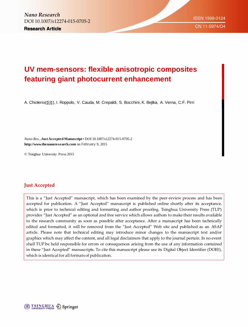
Our main finding is the first realization of a flexible, cheap, composite optoelectronic mem-
sensor, for which we describe the realization process (panel a), presenting a complete set of
structural, morphological and opto-electronic characterizations (panel b), and suggest a
technical symbol for the schematization of the device (panel c).

2
UV mem-sensors: flexible anisotropic composites featuring giant photocurrent enhancement
A. Chiolerio*, I. Roppolo, V. Cauda, M. Crepaldi, S. Bocchini, K. Bejtka, A. Verna, C.F.
Pirri
Dr. A. Chiolerio*, Dr. I. Roppolo, Dr. V. Cauda, Dr. M. Crepaldi, Dr. S. Bocchini, Dr. K.
Bejtka, Mr. A. Verna, Prof. C.F. Pirri
Center for Space Human Robotics, Istituto Italiano di Tecnologia, Corso Trento 21, 10129
Torino, Italy
Corresponding Author: [email protected]
ABSTRACT
Mem-sensing devices may be fabricated conjugating the sensitivity of a transducer with a
non-volatile memory, using two separate components. We show how to fabricate a mem-
sensor using a single material with built-in sensing/memory capabilities, based on ZnO
microwires embedded in a photocurable resin and processed from liquid by vertically aligning
the microwires across the polymeric matrix using dielectrophoresis. This particular choice
results in a UV- photodetector, device widely applied in fields such as telecommunication,
health and defence, so far implemented using bulk inorganic semiconductors. However,
inorganic detectors suffer from very high production costs, brittleness, huge equipment
requirements and low responsivities. We propose here for the first time a hybrid UV mem-
sensor easy processable, reproducible and low-cost. ZnO-aligned composites produce a giant
photocurrent, with respect to the same having randomly distributed microwires. In particular
3
we efficiently exploit a mem-response, where the photocurrent carries memory of the last
electronic state experienced by the device when under test. Furthermore, we demonstrate the
non-equivalence of different wave profiles used during dielectrophoresis, as a pulsed wave is
able to induce order both in axis and orientation of the microwires, while a sine wave only
affects the orientation.
Keywords: Giant Photocurrent, Mem-sensors, ZnO, Photopolimerization, Dielectrophoresis
SHORT PAPER
Zinc oxide (ZnO) is a n-type semiconductor material featuring catalytic, electronic,
piezoelectric and optical properties [1]. It possesses high electron mobility, high thermal
conductivity, wide band gap (~3.37 eV), and large exciton binding energy (~60 meV) [2,3]. In
addition ZnO shows peculiar optical properties with an UV absorption in the range 200-350
nm and emission in the near UV and visible range from 500 to 600 nm [4,5]. ZnO structures
show a high isoelectric point (9.5), biocompatibility, and low impact on the environment at
the end of life cycle [6-9]. Monocrystalline and one-dimensional (1D) ZnO, thus in the form
of either micro- and nanowires shows a superior fatigue resistance and charge separation and
transfer properties, useful in either mechanical nanogenerators and photoelectrochemical
devices [9-11]. Furthermore ZnO nanomaterials are easy to fabricate and raw materials and
precursors are cheap and easily available. The combination of semiconducting and
piezoelectric properties has been addressed as the “piezotronic effect”, whereas the
combination of optical and piezoelectric properties gives rise to the so called “piezo-
phototronic effect” [12-14]. As previously mentioned, ZnO has great potentialities for optical
applications. One of the most exploited applications for ZnO is UV detection, and the high
sensitivity towards UV detection is explained by the presence of oxygen-related hole-trapping
states at their surface [15]. The photogeneration of charges, occurring in ZnO hybrid materials
4
under UV irradiation, leads to the use of such structures in UV sensors [16-18]. In particular,
quite recently nanocomposite structure, based on a semiconductive matrix incorporating a
dispersion of ZnO nanoparticles, was shown to result in extremely high responsivities, three
to four times better than inorganic ultraviolet photodetectors [19]. The photogeneration
mechanism involves adsorption of light and generation of Frenkel excitons on the surface of
the ZnO nanoparticles; subsequently electrons are blocked by traps, usually present in ZnO,
while holes are free to move through the polymer matrix and are collected by the external
circuit. Hence the photocurrent is mainly unipolar [19].
In this work we fabricated an ordered polymer composite by using microwires, exploiting
their structural anisotropy to produce alignments in a high frequency electric field
(dielectrophoretic alignment, DEPA) [20]. The experiments evidenced a significant effect of
the structuration of the composite materials on their electrical and sensing properties;
moreover the material carries as built-in the capability of acting both as a transducer and as a
memory device.
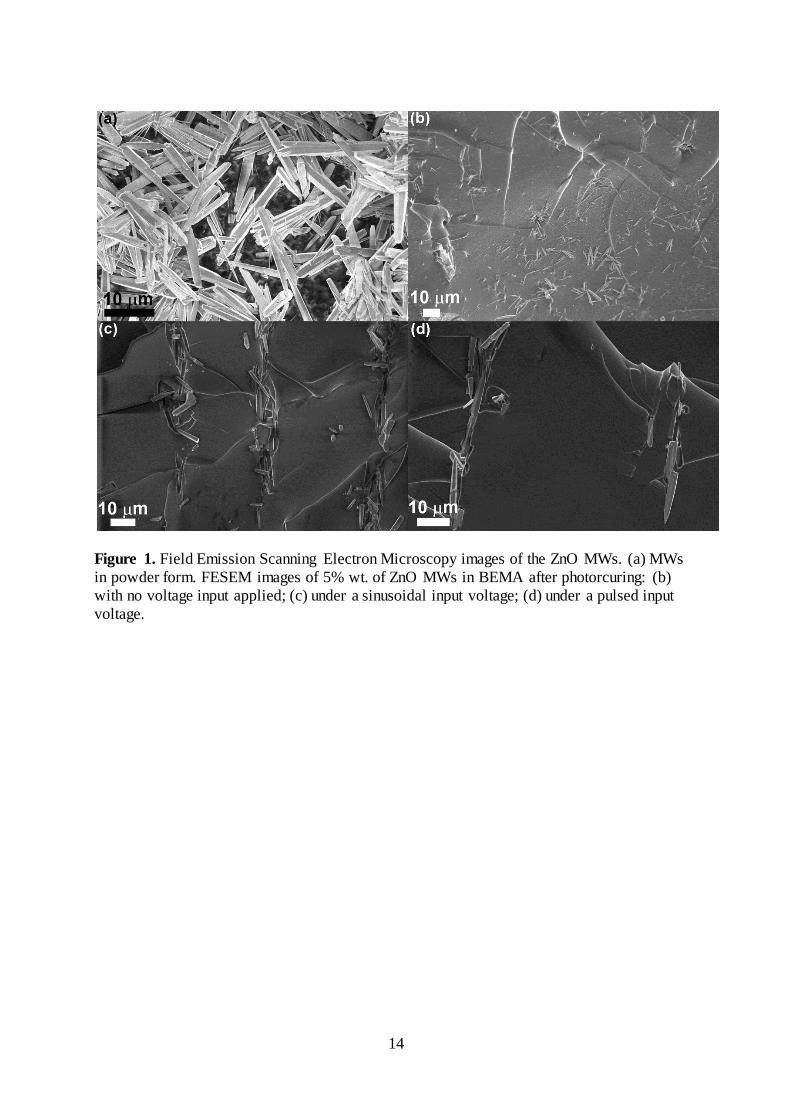
ZnO microwires (MWs) with a typical length of 5-20 µm and a diameter of 400-600 nm were
obtained by a highly reproducible and scalable hydrothermal synthesis. The FESEM image of
the representative sample is shown in Figure 1a. To achieve structural anisotropy, ZnO
microwires (MWs) were first dispersed (in different amounts, i.e. 0.5, 5 and 10 wt.%) in
liquid methacrylate monomers and then aligned in a container designed for this purpose (see
Figure S-1 in the ESM). The container includes the following parts: a brass bottom electrode,
a polytetrafluoroethylene (PTFE) spacer, a Fluorine-doped Tin Oxide (FTO) coated glass as
top electrode, a brass sheet as electric contact to the top electrode, a polymethylmethacrylate
(PMMA) plate, two PTFE pipes and polydimethylsiloxane (PDMS) o-rings. During the
DEPA, the liquid mixture inside the container was exposed to UV light and photocuring of
the methacrylic resins was run to achieve, at the end of the process, solid but flexible
nanostructured films. In particular we used both sinusoidal and pulsed input voltages to align

5
the ZnO MWs inside the polymeric matrix and we also fabricated a random composite, i.e.
without the application of the DEPA signal. The arbitrary signal generator was set to generate
both sine waves (100V peak) and pulsed (duty cycled) waves, 200 V peak, period 10 ms, duty
cycle 10% to electrically stimulate the samples and generate a very high electric field for the
MW alignment. As the impedance of the amplifier became comparable to the sample
impedance during curing, we observed a voltage decrease from 100 to 10 V with time
constants on the order of 5s, when using sine waves. We observed convergence towards a low
voltage limit: this fact indicates that the impedance was stabilized once the MWs were fully
aligned. The voltage decrease was observed for the pulsed waves as well, which had all
positive voltage values. The peak level decreased from 200 V to about 10 V to indicate the
build-up of a rectifying junction. This first experimental observation tells us that the two
waves are not equivalent, in affecting MW alignment degree.
These composites were then deeply characterized both morphologically and structurally to
evaluate the successful alignment of the ZnO MWs.
Figures 1b-d show the cross-section images of a selected set of composite samples containing
5 wt.% of ZnO MWs, including the reference sample and the composites subjected to the
DEPA process. Composites with other concentrations, i.e. 0.5 and 10 wt.%, show similar
structuration of the MWs inside the photocured resin. The reference sample, prepared by
dispersion of the ZnO MWs in the polymeric matrix and then photocured without the
application of the electric field, shows a random and almost homogeneous distribution of the
MWs in the BEMA matrix (Figure 1b). In contrast, the composite samples which were
subjected to the intense electric field clearly show an expected clustering and alignment of the
MWs in a head-to-tail configuration along the electric field lines, as shown in Figure 1c and d
for sinusoidal and pulsed input voltages respectively.
X-ray diffraction was used to investigate the ZnO MWs orientation and alignment within the
matrix, and the spectra are shown in Figure S-3 of the ESM. The sharp diffraction peaks
6
indicate high purity and degree of crystallinity of the powder. Similarly, the diffraction
patterns of the reference composites obtained without the application of the electric field show
all the diffraction peaks of ZnO, confirming a non-preferential alignment. In contrast, the
XRD patterns of the composite materials subjected to the DEPA process under both
sinusoidal and pulsed input voltages show a predominance of the (002) reflection, thus
indicating a preferential orientation of the ZnO MWs within the BEMA matrix. The relative
intensity among the (002) reflection and the other two, i.e. (100) and (010), is a direct
indication of the alignment degree of the MWs: the higher this ratio, the higher the
preferential vertical alignment of the MWs throughout the polymeric matrix. For
compositions of 0.5 and 10 wt.% of ZnO MWs, the highest level of alignment is obtained
with photocuring under sinusoidal input voltage (see Table S-1). This is in line with the
FESEM observations, shown in Figure 1.
UV-Visible measurements performed on the composite materials containing ZnO MWs
(Figure S-6 of the ESM) show a great loss of transparency when compared with the neat
matrix. However the reference composites in which the ZnO were randomly oriented
presented always the lower transparency indicating a greater light scattering than the oriented
composites. The measurements on the BEMA matrices containing oriented ZnO NWs
confirmed the results of XRD experiments. In fact ZnO MWs composite samples better
aligned under electrical field (see Table S-1) showed higher transparency. This could be
attributed to lower light scattering when the fillers are oriented in the direction parallel to the
incident light.
Direct current measurements for both the in plane and out of plane configurations are reported
in Figure S-8 of the ESM. In the in plane configuration, the most conductive materials (in the
range of 106 Ω∙cm) are those generated with sinusoidal electric field, almost regardless of
ZnO MWs content: 5 wt.% is indeed more conductive than 10 wt.%, while 0.5 wt.% is the
less conductive one.
7
The DC anisotropy, that is the ratio between in plane and out of plane current density, is
presented for all the samples in Figure S-9 of the ESM. The higher the ratio, the higher the
measured electrical DC anisotropy. The highest electrical DC anisotropy observed is that
induced by the pulsed electric field during photocuring for all concentrations of ZnO. The
highest anisotropy value obtained is as high as 300 in the case of BEMA matrix with 0.5 wt.%
of ZnO MWs. This is consistent with a reduced hopping, resulting from ZnO alignment along
the electric field direction (out of plane), and with an increased efficiency in hopping obtained
by orientation in the pulsed field, if compared to the sinusoidal one. So far, electrical
measurements have contributed in evidencing an effect which is not seen by means of other
structural characterizations (as XRD / UV-Vis, already discussed). As expected, randomly
oriented samples feature a random electrical DC anisotropy around 1 (isotropic response).
Interestingly, some of the responses are asymmetrical: all low-content ZnO samples
(triangles) feature an asymptotic curve crossing the axis E=0, diverging towards minus
infinity in quadrant I and towards plus infinity in quadrant II. This means that in their case the
out-of-plane current density goes to zero better than the in-plane one. It is easy to imagine that
low-content ZnO samples tested perpendicularly have smaller conduction mechanisms than
when tested in-plane, where the surface charge diffusion (leakage) is relatively higher, while
high-content ZnO samples are such that volume effects are relatively more important.
Impedance spectroscopy analyses were undertaken to test frequency response of the device
and to better understand electronic phenomena occurring in the materials (measurements
available in the SI). Samples having 0.5 wt.% content of ZnO MWs feature a response
typically more similar to that of pure BEMA (the evidence comes from phase curves, in the
range between 100 Hz and 10 kHz). For what concerns impedance modulus, randomly
oriented samples behave differently from pure BEMA matrix. The effect of an electric field
upon photocuring, either pulsed or sinusoidal, results in radically different properties: a lower
modulus for 0.5 wt.% ZnO MWs, a higher modulus for 5 wt.% and a split result for 10 wt.%,
8
where a sinusoidal field reduces the modulus, and a pulsed field increases it. Concerning the
impedance phase graphs, the pure BEMA matrix and certain samples (mainly the randomly
oriented having 0.5 wt.%) feature a high field negative capacitance effect (phase saturation at
+ 90°), depending on the amount of ZnO incorporated in the composites. Negative
capacitance was theoretically explained and already observed in similar systems [21-23].
Another interesting feature emerging from out of plane measurements is that impedance
modulus is minimum for randomly oriented samples, while samples oriented both with
sinusoidal and pulsed fields show intermediate properties if compared to the pure matrix.
A useful exploitation of impedance and IV properties of the studied samples as a quasi-ideal
voltage controlled phase shifter is presented in Figure 2a and b (10 wt.% ZnO MWs-BEMA
composite was chosen as an example, having the most relevant response). Depending on the
working frequency, it is observed how samples prepared with different electric field
treatments produce either a phase-shifting or a constant phase response. In the former case,
the phase abruptly changes between + 90° and – 90°, depending on the DC voltage applied,
the threshold being ±5 V. We have also observed that, regardless of the photocuring voltage
submitted to samples, those able to produce a phase shifting were the same exhibiting
negative impedance phase, i.e. negative capacitance. A possible explanation of what we
observed is that the trap barrier height, function of applied DC voltage, may be easily tuned
deeply reversing the phase from negative to positive and vice-versa. ZnO MWs, in their
crystalline structure, always result in one side O-terminated and the other Zn-terminated; this
means they have not only a major axis, but also an orientation as a vector. We have that the
sinusoidal DEP field is affecting this preferential orientation of each wire within the chain
composed by aligned wires. Random and sinusoidal waves do not succeed in orienting head-
to-tail wires in proximity and the behavior is that of a bulk semiconductor (capacitor). Pulsed
waves on the contrary, able to affect also the orientation, result in improved dielectric
interaction of the oriented dipoles.
9
A typical photocurrent enhancement pattern is shown in Figure 2c, where three samples
having the same composition (BEMA + 5 wt.% ZnO MWs) but subjected to different
production processes (randomly oriented, sinusoidal field and pulsed field) are compared.
During the measurements a null voltage was maintained across the circuit, resulting in bipolar
curves (negative enhancement for random and sinusoidal samples, positive for pulsed
samples). The photocurrent sign depends on the overall properties of each sample, in
particular when the sample is structurally asymmetric as those produced with a pulsed field, it
is possible to measure different photocurrent signs by simply changing the surface
(recto/verso). The response depends upon the orientation of the sample itself, hence it has two
non-equivalent surfaces, and the property occurs only when the voltage drop across the
sample is zero.
Data recorded during the experiments are summarized in Table S-2.
A typical response is shown in Figure 2d, where a sample of BEMA + 0.5 wt.% ZnO with
random distribution (zero field) is measured while maintaining a voltage drop of 100 V across
the sample. The time response is extremely fast, since the photocurrent enhancement
consistent with a UV radiation power of 50 mW cm-2 increases up to 900 % in only 20 s. Also
the dark current is remarkably low, being in the nA range at zero applied bias.
In view of an application as UV sensor, the choice for the optimal composition goes through a
trade-off between many parameters: response stability, photocurrent on/off ratio, total
enhancement, eventual bipolar operation. Even though the highest photocurrent enhancement
(1087 %) was obtained for the randomly oriented 0.5 wt.% sample, its stability is average
(10% baseline variation between subsequent measurements) and the baseline amplitude also
average (90 nA). The optimal choice is the pulsed 5 wt.% sample, having bipolar operability,
great stability (0.1% under reverse bias), featuring a photocurrent enhancement close to 500%
and a baseline of 330 nA (see Table S-2 for numerical data).
10
Flexible devices, encapsulated in copper electrodes as described before, were also tested
under cyclic stimulation. By performing closed loops in the IV plane, we could also observe
an hysteretic response, as that shown in Figure 3a and b, under different UV light intensities.
This pinched hysteresis loop is characteristic of memristors, as described in several recent
papers, i.e. devices that have shown to be good candidates for the fabrication of future
memories and computational elements, implementing locally passive storage at electrical
level [24-26]. Taking the first derivative of the IV hysteretic curves (i.e. the conductance
curves in Figure 3b), it is easier to notice that the first point when applied voltage is zero has
different conductances and slopes. The non-zero current under zero bias (Figure 3a) is to be
interpreted as a differential resistance condition, between two subsequent states: the previous
state undergone is that corresponding to –(maximum voltage) and is the last experimental
point of the previous cycle, while the actual state is that at zero bias, taken after the setting of
a new value for the optical power density, which is the first point of the actual cycle.
In light of the best performances obtained here we only show the sample BEMA + 10wt.%
ZnO NWs synthesized under pulsed field (measurements performed on the others samples are
presented in ESM). Since the measurements were performed for increasing the UV density
from dark to 90 mWcm-2, we can conclude that our composite device is actually a mem-
sensor, i.e. not only a sensor whose response is a function of the applied radiation field, but
also a sensor whose response is a function of the history of previous states [27-28]. A further
proof of this behavior is given in Figure 3c, where the differential conductance is plotted
against UV power density, for two loci of the hysteresis loop: the first part of it, starting from
0 V (off-state memory effect of the mem-sensor), actually carrying information of the
previous state, and the middle of the hysteresis loop (again 0 V crossing), carrying
information on the instantaneous state (classic sensor).
Finally, as we may not exclude pyroelectric effects caused by sample heating during exposure
to UV light, we have measured the current variation over time, under constant light density,

11
and plotted it against optical power (Figure 3d). The current variation in steady conditions is
easily seen as a linear slope (Figure 2c and 2d), the higher the light intensity, the steeper the
slope. It is seen that a quadratic polynomial cumulative fit succeeds in providing a clear
picture of the fact that the current variation depends on a sample temperature, that in turn is a
quadratic function of the heating source power density [29].
ACKNOWLEDGEMENTS
The authors would like to thank Dr. Edvige Celasco for the field emission scanning electron
microscopy image and Mr. Alessandro Nesca for his precious help in the fabrication of the
microfluidic system for DEP.
Electronic Supplementary Material: Supplementary material (methods, dielectrophoretic
alignment, XRD and UV-Vis spectra, IV measurements, impedance spectroscopy curves) is
available in the online version of this article at
http://dx.doi.org/10.1007/***********************
REFERENCES
[1] L.Vayssieres, K. Keis, A. Hagfeldt, S.-E. Lindquist, Chem. Mater. 13, 4395-4398
2001.
[2] U. Ozgur, Y. I. Alivov, C. Liu, A. Teke, M. A. Reshchikov, S. Dogan, V. Avrutin, S.-J.
Cho, H. Morkoc, J. Appl. Phys. 98, 041301 2005.
12
[3] Z. R. Tian, J. A. Voigt, J. Liu, B. McKenzie B, M. J. McDermott, M. A. Rodriguez, H.
Konishi, H. Xu, Nat. Mater. 2, 821-826 2003.
[4] S. A. Wilson, R. P. J. Jourdain, Q. Zhang, R. A. Dorey, C. R. Bowen, M. Willander, Q.
Ul Wahab, S. M. Al-hilli, O. Nur, E. Quandt, C. Johansson, E. Pagounis, M. Kohl, J. Matovic,
B. Samel, W. van der Wijngaart, E. W. H. Jager, D. Carlsson, Z. Djinovic, M. Wegener, C.
Moldovan, R. Iosub, E. Abad, M. Wendlandt, C. Rusu, K. Persson, Mat. Sci. and Eng.: R:
Reports 56, 1-129 2007.
[5] D. W. Bahnemann, C. Kormann, and M. R. Hoffmann, J. Phys. Chem. 91, 3789-3798
1987.
[6] J. Gomez, O. Tigli, J. Mater. Sci. 48, 612-624 2013.
[7] S. Xu, Z. L. Wang, Nano Res. 4, 1013-1098 2011.
[8] V. Cauda, R. Gazia, S. Porro, S. Stassi, G. Canavese, I. Roppolo, A. Chiolerio,
Nanostructured ZnO materials: synthesis, properties and applications (Springer Verlag, Berlin,
2014) in Handbook of Nanomaterial Properties, B. Bhushan, D. Luo, S. R. Schricker, W.
Sigmund, S. Zauscher Eds..
[9] C. Ottone, S. Stassi, P. Motto, M. Laurenti, D. Demarchi, V. Cauda, ZnO nanowires:
synthesis approaches and electrical properties (Nova Publishers, 2014) in Nanowires:
Synthesis, Electrical Properties and Uses in Biological Systems, N. Columbus Ed..
[10] H. D. Espinosa,R. A. Bernal,M. Minary-Jolandan, Adv. Mater. 24, 4656–4675 2012.
[11] S. Hernández, V. Cauda, A. Chiodoni, S. Dallorto, A. Sacco, D. Hidalgo, E. Celasco,
C. F. Pirri, ACS Appl. Mater. and Inter., 2014, ISSN:1944-8244, doi: 10.1021/am501379m.
[12] Y. Zhang, X. Yan, Y. Yang, Y. Huang, Q. Liao, J. Qi, Adv. Mater. 24, 4647-4655
2012.
[13] Y. Zhang, Y. Liu, Z. L. Wang, Adv. Mater. 23, 3004-3013 2011.
[14] S. Xu, W. Guo, S. Du, M. M. T. Loy, N. Wang, Nano Lett. 12, 5802-5807 2012.
13
[15] C. Soci, A. Zhang, B. Xiang, S. A. Dayeh, D. P. R. Aplin, J. Park, X. Y. Bao, Y. H. Lo,
D. Wang, Nano Lett. 7, 1003 2007.
[16] Y. N. He, W. Zhang, S. C. Zhang, X. Kang, W. B. Peng, Y. L. Xu, Sensors and
Actuators a-Physical 181, 6-12 2012.
[17] Y. Z. Jin, J. P. Wang, B. Q. Sun, J. C. Blakesley, N. C. Greenham, Nano Lett. 8, 1649-
1653 2008.
[18] C. S. Lao, M.-C. Park, Q. Kuang, Y. Deng, A. K. Sood, D. L. Polla, Z. L. Wang, J.
Am. Chem. Soc. 129, 12096-12097 2007.
[19] F. Guo, B. Yang, Y. Yuan, Z. Xiao, Q. Dong, Y. Bi and J. Huang, Nat. Nanotec. 7,
798-802 2012.
[20] D. Wang, et al., App. Phys. Lett. 90, 103110 2007.
[21] H.L. Kwok, Solid-State Electronics, 47, 1089 2003.
[22] S. Bocchini, A. Chiolerio, S. Porro, D. Accardo, N. Garino, K. Bejtka, D. Perrone and
C.F. Pirri, J. Mater. Chem. C 1, 5101-5109 2013.
[23] A. Chiolerio, S. Bocchini, S. Porro, Adv. Funct. Mater. 24, 3375-3383 2014.
[24] D. I. Son, C. H. You, W. T. Kim, J. H. Jung, T. W. Kim, App. Phys. Lett., 94, 132103
2009.
[25] D. I. Son, C. H. You, J. H. Jung, T. W. Kim, App. Phys. Lett., 97, 013304 2010.
[26] M. P. Sah, K. Hyongsuk, L. O. Chua, IEEE Circuits and Systems Magazine, 14, 12-36
2014.
[27] Z. Fan, X. Fan, A. Li and L. Dong, Nanorobotic in situ characterization of nanowires
memristors and “memsensing”, IEEE/RSJ International Conference on Intelligent Robots and
Systems (IROS), November 3-7, 2013, Tokyo, Japan.
[28] X. Wang, Y. Chen, Y. Gu and H. Li, IEEE Electron Device Letters, 31, 20-22 2010.
[29] Y. Yang, W. Guo, K.C. Pradel, G. Zhu, Y. Zhou, Y. Zhang, Y. Hu,
L. Lin and Z.L. Wang, Nano Letters, 12(6), 2833-2838 2012.
14
Figure 1. Field Emission Scanning Electron Microscopy images of the ZnO MWs. (a) MWs
in powder form. FESEM images of 5% wt. of ZnO MWs in BEMA after photorcuring: (b)
with no voltage input applied; (c) under a sinusoidal input voltage; (d) under a pulsed input
voltage.

15
Figure 2. Impedance phase at a fixed AC stimulus 1 kHz (a), 100 kHz (b), as a function of the
DC bias, measured on composites having the 10 wt.% content of ZnO MWs. Photocurrent
enhancement measurements for the BEMA-ZnO composites. (c) Plots for BEMA with 5 wt.%
ZnO MWs, in the three different fabrication cases: no electric field (black line), sinusoidal
field (red line), pulsed field (blue line). The three levels of power correspond to 50 (P1), 30
(P2) and 10% (P3) of the total output power. (d) Photocurrent enhancement measurement for
the composite BEMA with 0.5 wt.% ZnO randomly dispersed MWs.

16
Figure 3. Mem-sensor nanocomposite devices response. (a) : cyclic IV measurements under
UV light ; (b): first derivative (memconductance) from IV measurements; in the inset:
proposed electronic symbol of the UV mem-sensor.(c) Mem-sensor differential conductance
in two cases: off-state (mem-sensor, black stars) carrying information on the previous state,
and zero-voltage crossing state (classical sensor, red open dots). (d) Pyroelectric contribution
to the photocurrent, computed as variation in the current over time, versus optical power
density, for the sample BEMA – 10wt.% ZnO. The quadratic polynomial fit is a cumulative
one.
Related Documents