Sensors and Actuators B 223 (2016) 429–439 Contents lists available at ScienceDirect Sensors and Actuators B: Chemical jo ur nal home page: www.elsevier.com/locate/snb Enhanced NO 2 gas sensing performance of bare and Pd-loaded SnO 2 thick film sensors under UV-light irradiation at room temperature Fahimeh Hooriabad Saboor a,b , Taro Ueda b , Kai Kamada b , Takeo Hyodo b , Yadollah Mortazavi a,c , Abbas Ali Khodadadi a , Yasuhiro Shimizu b,∗ a Catalysis and Nanostructured Materials Research Laboratory, School of Chemical Engineering, College of Engineering, University of Tehran, Tehran, Iran b Graduate School of Engineering, Nagasaki University, 1-14 Bunkyo-machi, Nagasaki 852-8521, Japan c Nanoelectronics Centre of Excellence, University of Tehran, P.O. Box 11365-4563, Tehran, Iran a r t i c l e i n f o Article history: Received 17 February 2015 Received in revised form 30 July 2015 Accepted 14 September 2015 Available online 28 September 2015 Keywords: NO2 Gas sensor UV SnO2 Pd functionalization a b s t r a c t NO 2 gas sensing performance of bare and Pd-loaded SnO 2 thick film sensors were measured under UV-light irradiation, using a UV-LED of 365 nm wavelength and light intensities ranging from 0 to 137 mW cm −2 at room temperature (30 ◦ C). Template free conventional and microwave-assisted hydrothermal methods were applied to synthesize SnO 2 powder with different specific surface areas and morphologies (rod-shape and nanoparticle). Two different Pd-loaded SnO 2 (0.03 and 0.1 wt%) pow- ders were also prepared by a simple wet-impregnation method. XRD, FE-SEM/SEM, XPS, BET surface area and BJH pore size distribution measured with N 2 adsorption isotherms were utilized to character- ize structural and morphological characteristics of all the samples. The results clearly confirmed that the presence of a low amount of Pd could effectively enhance the response value to 5 ppm NO 2 gas and shorten the recovery time under the UV-light irradiation so that the sensor loaded with 0.1 wt% Pd (0.1Pd MH1 400 sensor) showed the largest improvement in response value (almost 11 times) and recovery time (around 27 s) compared with the bare SnO 2 sensor (MH1 400) at an UV-light intensity of 79 mW cm −2 . This enhancement is most likely due to the role of Pd in facilitating the sensing reactions via producing additional NO 2 adsorption sites on the SnO 2 surface. Moreover, in the present study, the SnO 2 sensor which was fabricated from as-synthesized, i.e. uncalcined, powder (MH1) showed the high- est response (over 3000) compared with other sensors under an UV-light intensity of 7 mW cm −2 with a recovery time of about 48 s. The drastic decrease in the resistance in air of this sensor under the UV-light irradiation may be a possible reason for the highest response value. It was also revealed that high NO 2 response could be achieved only at the optimum conditions of both the number of the NO 2 adsorption sites (optimum specific surface area) and the electron density in the bulk under the UV-light irradiation. © 2015 Elsevier B.V. All rights reserved. 1. Introduction Nitrogen dioxide (NO 2 ), as one of the main air pollutants, which causes smog and acid rain in metropolitan areas as well as ozone formation in the atmosphere [1], can be detected by different types of sensors such as piezoelectric [2], electrochemical [3] and semi- conductor gas sensors [4]. Because of their simplicity in fabrication, low cost, high sensitivity and long-term stability, metal oxide semi- conductors such as WO 3 , In 2 O 3 , NiO, ZnO and SnO 2 have been widely studied as the sensing materials for NO 2 detection in recent years. In order to ensure a complete desorption of NO 2 molecules from the surface of the semiconductor gas sensors, they are usually ∗ Corresponding author. E-mail address: [email protected] (Y. Shimizu). operated at elevated temperatures [4–6]. Another complication is the structural long-term instability due to the sintering effects on the metal oxide grain boundaries at elevated temperatures [7,8]. However, long response/recovery times and sometimes low sensi- tivity have been reported as the main drawbacks for SnO 2 thin film sensors operated at room temperature [9]. Several approaches such as functionalization, loading of noble metals including Pd, Pt and Au [10,11], application of an electro- static field [12], core/shell structure formation [13] and UV-light irradiation [5,7,14–16] have been reported by several researchers to reduce working temperature of semiconductor metal oxide gas sensors. There are several reports in the literature [14–23] on the gas sensing enhancement by UV-light irradiation at room tem- perature for both reducing and oxidizing gases. Enhancement of the NO 2 response was also achieved by the UV-light irradiation on a SnO 2 thin film at room temperature [14]. Mishra et al. [17] http://dx.doi.org/10.1016/j.snb.2015.09.075 0925-4005/© 2015 Elsevier B.V. All rights reserved.

Welcome message from author
This document is posted to help you gain knowledge. Please leave a comment to let me know what you think about it! Share it to your friends and learn new things together.
Transcript

Et
FYa
b
c
a
ARRAA
KNGUSP
1
cfoclcwyf
h0
Sensors and Actuators B 223 (2016) 429–439
Contents lists available at ScienceDirect
Sensors and Actuators B: Chemical
jo ur nal home page: www.elsev ier .com/ locate /snb
nhanced NO2 gas sensing performance of bare and Pd-loaded SnO2
hick film sensors under UV-light irradiation at room temperature
ahimeh Hooriabad Saboora,b, Taro Uedab, Kai Kamadab, Takeo Hyodob,adollah Mortazavia,c, Abbas Ali Khodadadia, Yasuhiro Shimizub,∗
Catalysis and Nanostructured Materials Research Laboratory, School of Chemical Engineering, College of Engineering, University of Tehran, Tehran, IranGraduate School of Engineering, Nagasaki University, 1-14 Bunkyo-machi, Nagasaki 852-8521, JapanNanoelectronics Centre of Excellence, University of Tehran, P.O. Box 11365-4563, Tehran, Iran
r t i c l e i n f o
rticle history:eceived 17 February 2015eceived in revised form 30 July 2015ccepted 14 September 2015vailable online 28 September 2015
eywords:O2
as sensorVnO2
d functionalization
a b s t r a c t
NO2 gas sensing performance of bare and Pd-loaded SnO2 thick film sensors were measured underUV-light irradiation, using a UV-LED of 365 nm wavelength and light intensities ranging from 0to 137 mW cm−2 at room temperature (30 ◦C). Template free conventional and microwave-assistedhydrothermal methods were applied to synthesize SnO2 powder with different specific surface areasand morphologies (rod-shape and nanoparticle). Two different Pd-loaded SnO2 (0.03 and 0.1 wt%) pow-ders were also prepared by a simple wet-impregnation method. XRD, FE-SEM/SEM, XPS, BET surfacearea and BJH pore size distribution measured with N2 adsorption isotherms were utilized to character-ize structural and morphological characteristics of all the samples. The results clearly confirmed thatthe presence of a low amount of Pd could effectively enhance the response value to 5 ppm NO2 gasand shorten the recovery time under the UV-light irradiation so that the sensor loaded with 0.1 wt%Pd (0.1Pd MH1 400 sensor) showed the largest improvement in response value (almost 11 times) andrecovery time (around 27 s) compared with the bare SnO2 sensor (MH1 400) at an UV-light intensity of79 mW cm−2. This enhancement is most likely due to the role of Pd in facilitating the sensing reactionsvia producing additional NO2 adsorption sites on the SnO2 surface. Moreover, in the present study, theSnO2 sensor which was fabricated from as-synthesized, i.e. uncalcined, powder (MH1) showed the high-
−2
est response (over 3000) compared with other sensors under an UV-light intensity of 7 mW cm with arecovery time of about 48 s. The drastic decrease in the resistance in air of this sensor under the UV-lightirradiation may be a possible reason for the highest response value. It was also revealed that high NO2response could be achieved only at the optimum conditions of both the number of the NO2 adsorptionsites (optimum specific surface area) and the electron density in the bulk under the UV-light irradiation.
. Introduction
Nitrogen dioxide (NO2), as one of the main air pollutants, whichauses smog and acid rain in metropolitan areas as well as ozoneormation in the atmosphere [1], can be detected by different typesf sensors such as piezoelectric [2], electrochemical [3] and semi-onductor gas sensors [4]. Because of their simplicity in fabrication,ow cost, high sensitivity and long-term stability, metal oxide semi-onductors such as WO3, In2O3, NiO, ZnO and SnO2 have been
idely studied as the sensing materials for NO2 detection in recentears. In order to ensure a complete desorption of NO2 moleculesrom the surface of the semiconductor gas sensors, they are usually
∗ Corresponding author.E-mail address: [email protected] (Y. Shimizu).
ttp://dx.doi.org/10.1016/j.snb.2015.09.075925-4005/© 2015 Elsevier B.V. All rights reserved.
© 2015 Elsevier B.V. All rights reserved.
operated at elevated temperatures [4–6]. Another complication isthe structural long-term instability due to the sintering effects onthe metal oxide grain boundaries at elevated temperatures [7,8].However, long response/recovery times and sometimes low sensi-tivity have been reported as the main drawbacks for SnO2 thin filmsensors operated at room temperature [9].
Several approaches such as functionalization, loading of noblemetals including Pd, Pt and Au [10,11], application of an electro-static field [12], core/shell structure formation [13] and UV-lightirradiation [5,7,14–16] have been reported by several researchersto reduce working temperature of semiconductor metal oxide gassensors. There are several reports in the literature [14–23] on the
gas sensing enhancement by UV-light irradiation at room tem-perature for both reducing and oxidizing gases. Enhancement ofthe NO2 response was also achieved by the UV-light irradiationon a SnO2 thin film at room temperature [14]. Mishra et al. [17]
4 d Actu
tgsroois[eNitfoSt[so
euarwaaa
2
2
mvD(wfnSt
fhna
(at
TS
30 F.H. Saboor et al. / Sensors an
heoretically showed that sensitivity of semiconductor metal oxideas sensors should improve with increasing the incident light inten-ity and decreasing the grain size. Moreover, more recently someesearchers have experimentally found that the sensing responsef ZnO under the UV-light irradiation at room temperature is notnly dependent on the light wavelength and its intensity, butt can also be affected by the kind of target gases, crystal/grainize and photo-generated charge efficiency of the sensing material15,16]. Recently, Lee et al. [18–20] studied the gas sensing prop-rties of ZnO and ZnS functionalized with some noble metals toO2 gas and an enhancement in sensor response for functional-
zed semiconductors was reported. Moreover, enhanced responseo 200 ppm LPG at room temperature for SnO2 thin films with dif-erent thickness has been achieved by applying a combined effectf UV-light irradiation and the presence of a Pt catalyst on thenO2 surface [21]. Until now, many studies have been reported onhe NO2 gas sensing properties of single [5,14,22] and composite1,4,23] metal oxide materials under UV-light irradiation, while fewtudies have examined functionalized or noble metal-loaded metalxide materials under the UV-light irradiation [18–20].
In the present study we investigated the NO2 gas sensing prop-rties of SnO2 thick film sensors at room temperature (30 ◦C)nder the UV-light irradiation with different intensities andlso examined the effect of Pd-loading on response values andesponse/recovery time of the SnO2 sensors. SnO2 nanoparticlesere synthesized by template-free conventional and microwave-
ssisted hydrothermal methods with different specific surface areand morphologies, and Pd–SnO2 nanoparticles were prepared via
simple wet impregnation method.
. Experimental
.1. Materials and synthesis method
In this study we synthesized SnO2 nanoparticles by applyingicrowave-assisted hydrothermal (CEM Corp., MARS5) and con-
entional hydrothermal methods without using any templates.ifferent synthesis parameters, including tin precursor types
SnCl4 and SnCl2), concentration, synthesis time and temperature,ere applied to obtain different morphologies and specific sur-
ace area of SnO2 samples. We also synthesized Pd-loaded SnO2anoparticles as samples by using a wet impregnation method.nCl4·5H2O, SnCl2·2H2O and NaOH were used as raw materials forhe SnO2 synthesis and Pd(NO3)2 as a Pd precursor.
SnO2 samples thus prepared are denoted as MHx y and CH yor ones prepared by the microwave assisted and conventionalydrothermal synthesis, respectively (x: sample number, y: calci-ation temperature). The as-synthesized sample is just referred tos MHx.
In a typical synthesis, same volume of tin chloride solutionSnCl4 or SnCl2) and NaOH solution were mixed together with
water/EtOH mixture in a predetermined volume ratio. Theotal volume of the mixture for all the samples synthesized by
able 1ynthesis conditions of SnO2 samples.
Sample Tin chloride (M) NaOH (M) Water/EtOHvolume ratio
MH1 0.15a 0.9 1
MH2 0.05b 0.05 No EtOH
MH3 0.5a 5 2
CH 0.15a 0.9 1
a SnCl4·5H2O was used as a Tin precursor.b SnCl2·2H2O was used as a Tin precursor.
ators B 223 (2016) 429–439
microwave-assisted and conventional hydrothermal methods wasaround 20 and 50 ml, respectively. The synthesis conditions for allthe samples are listed in Table 1. Following the stirring for severalminutes, the milky mixture was transferred into a Teflon vesseland sealed in a hydrothermal autoclave (100 ml Teflon vessel formicrowave hydrothermal synthesis and 75 ml Teflon-lined stain-less steel autoclave for conventional hydrothermal synthesis). Theautoclave was heated to the desired temperature and kept at thesame temperature for desired time (see Table 1). After self-coolingdown, all the samples were separated by centrifugation and washedseveral times with deionized water and EtOH. Finally, the powderwas dried at 60 ◦C overnight and calcined at desired temperaturefor 2 h.
We applied a wet impregnation method to load Pd (0.03,0.1 wt%) on some of SnO2 samples (MH1 400 and CH 500). In a typ-ical synthesis, the desired amount of Pd(NO3)2·2H2O was added to0.2 g of SnO2 powder. The mixture was dispersed in 20 ml of waterand was subjected to ultrasonication for 5 min. Thereafter it washeated on a heater-stirrer until it was completely dried. After grind-ing for 15 min, the final powder was heated at 200 ◦C for 2 h underH2 gas flowing (100 ml min−1) in order to reduce to metallic Pd.
2.2. Characterization
The morphologies of all the powders were observed by FE-SEM(JEOL Ltd., JSM-7500F) or SEM (JEOL Ltd., JCM-5700ME). Crystalphase and structure of the powders were characterized by X-raydiffraction analysis (XRD; Rigaku Corp., RINT2200) by using Cu K�radiation (40 kV, 40 mA) and their crystallite size (CS) was calcu-lated with a help of Scherrer equation. The specific surface areaand pore size distribution were measured by BET and BJH methodsusing the N2 adsorption isotherm (Micromeritics, Tristar3000). Thechange in oxidation states of the sensor materials was measuredwith X-ray photoelectron spectroscopy by using Al K� radiation(XPS, Kratos, AXIS-ULTRA DLD) and the binding energy was cali-brated by using the C 1s level originating from usual contamination,e.g. organic compounds (284.5 eV). The average particle sizes (dBET)were obtained from BET specific surface area using Eq. (1).
dBET = 6000�SBET
(1)
where � (g cm−3) is the density of the samples and SBET is the spe-cific surface area (m2 g−1) measured by the BET method.
2.3. Sensor fabrication
The thick film sensors were fabricated by a screen-printingmethod. The paste of each sample was applied on the alumina sub-strate with previously printed a pair of interdigitated Pt electrodes
(gap size: ca. 200 �m), followed by calcination at 500 ◦C for 1 h. Gasresponse of these sensors was measured to 5 ppm NO2 balancedwith dry air in a flow apparatus (gas flow rate of 100 cm3 min−1)at room temperature (30 ◦C) under UV-light irradiation withStirring time (min) Synthesistemperature (◦C),time (h)
Calcinationtemperature (◦C)
40 190, 1 As-synthesized,400 and 500
30 190, 0.5 40015 240, 0.5 As-synthesized40 190, 24 500
d Actuators B 223 (2016) 429–439 431
d3wTUUtpsdaa
3
3
atiiPdrS5cotTa
mtstip
F00
Table 2BET specific surface area along with particle size of all samples.
Sample BET specificsurface area(m2 g−1)
Averageparticle size(nm)
MH1 88 10MH1 400 37 230.03Pd MH1 400 39 230.1Pd MH1 400 42 21MH1 500 17 51MH2 400 47 18MH3 6 37CH 500 13 66
F.H. Saboor et al. / Sensors an
ifferent intensities ranging from 0 to 137 mW cm−2. We utilized65 nm UV-LED (Asahi Spectra Co., Ltd.; LED light source, POT-365)ith a quartz window as UV source in all the gas sensing tests.
he wavelength range used (spectral bandwidth) of the appliedV-source was 365 ± 5 nm. The distance between the sensor andV-LED was kept constant at 10 mm. The sensors were first heat
reated at 200 ◦C for 1 h, followed by cooling down to room tem-erature under dry air before the UV-light irradiation to clean upensor surface from all adsorbed species. The sensor response isefined as the ratio (Rg/Ra) of sensor resistance in a sample gas bal-nced with air (Rg) to that in air (Ra). Recovery time (trec) is defineds the time to reach 80% of the initial resistance of the sensor in air.
. Results and discussion
.1. Characterization of samples
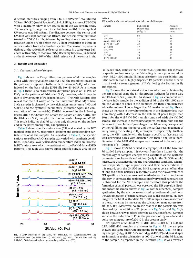
Fig. 1 shows the X-ray diffraction patterns of all the sampleslong with their crystallite sizes (CS). All the prominent peaks inhe pattern corresponded to the rutile structure of SnO2, which arendexed on the basis of the JCPDS file No. 41-1445. As is shownn Fig. 1 there is no characteristic diffraction peaks of Pd, PdO ordO2 in the patterns of Pd-loaded SnO2 powders, which may beue to low amounts of Pd loaded on SnO2. The XRD patterns alsoeveal that the full width at the half maximum (FWHM) of barenO2 samples is changed by the calcination temperature (400 and00 ◦C) and the synthesis parameters (precursor types and con-entration of raw materials). FWHM decreased in the followingrder: MH1 > MH2 400 > MH1 400 > MH1 500 > CH 500 > MH3. Forhe Pd-loaded SnO2 samples, there is no drastic change in FWHM.his result indicates that Pd particles only disperse on the surfacend in the pores among SnO2 nanoparticles.
Table 2 shows specific surface area (SSA) calculated by the BETethod using the N2 adsorption isotherm and corresponding par-
icle sizes of all the samples. As is evident in Table 2, the specific
urface area of bare SnO2 samples was varied with synthesis condi-ions. Especially, lower calcination temperature led to an increasen BET surface area which is consistent with the FWHM data of XRDatterns. This table also shows larger specific surface area of theig. 1. XRD patterns of (a) MH1, (b) MH1 400, (c) 0.03Pd MH1 400, (d).1Pd MH1 400, (e) MH1 500, (f) MH2 400, (g) MH3, (h) CH 500 and (i).1Pd CH 500 along with their calculated crystallite sizes (CS).
0.1Pd CH 500 20 43
Pd-loaded SnO2 samples than the bare SnO2 samples. The increasein specific surface area by the Pd-loading is more pronounced forthe 0.1Pd CH 500 sample. This may arise from two possibilities, oneis the contribution of highly dispersed Pd particles and the other isthat of surface rearrangement of SnO2 during the heating in H2atmosphere.
Fig. 2 shows the pore size distributions which were obtained bythe BJH method using the N2 desorption isotherm for some bareand Pd-loaded SnO2 samples. As shown in Fig. 2a, compared withthe bare SnO2 sample, by the addition of Pd to the MH1 400 sam-ple, the volume of pores in the diameter less than 6 nm increasedwhile the volume of pores larger than 10 nm decreased. Fig. 2b alsoshows an increase in the volume of pores in the diameter less than7 nm along with a decrease in the volume of pores larger than10 nm for the 0.1Pd CH 500 sample compared with the CH 500sample. The increase in the volume of pores less than 7 nm and thedecrease in the volume of pores larger than 10 nm may be explainedby the Pd filling into the pores and the surface rearrangement ofSnO2 during the heating in H2 atmosphere, respectively. Further-more, the MH1 sample with the largest specific surface area hadwell-developed pores with diameter less than 5 nm, while pore-diameter in the MH1 400 sample was measured to be mostly inthe range of 5–100 nm.
Fig. 3 shows FE-SEM or SEM micrographs of all the bare andPd-loaded SnO2 samples. It is obvious from these images that themorphology of samples changes with variations of the synthesisparameters, such as with and without (only for the CH 500 sample)microwave assistance during the hydrothermal synthesis, calcina-tion temperature, type of precursors and their concentrations. Inthis regard, both the CH 500 and MH3 samples consist of bundlesof long rod-shape particles, respectively, and their lower values ofBET specific surface area are considered to be ascribed to such mor-phology. In contrast, the agglomeration of very small nanoparticlesis observed for the MH1 sample and therefore this predicts theformation of small pores, as was observed the BJH pore size distri-bution for this sample shown in Fig. 2a. For the other SnO2 samplessynthesized by the microwave-assisted hydrothermal conditions,the agglomeration of small nanoparticles is also observed. FE-SEMimages of the MH1 400 and the MH1 500 samples show an increasein the particle size by increasing the calcination temperature from400 to 500 ◦C. Moreover, no drastic change in the particle size wasobserved by the addition of Pd (compare Fig. 3b–d and Fig. 3h,i).This is because Pd was added after the calcination of SnO2 samplesand also the reduction to Pd in the presence of H2 was done at aquite low temperature of 200 ◦C in the present study.
XPS spectra of Sn 3d of MH1, MH1 400, 0.03Pd MH1 400 and0.1Pd MH1 400 samples are shown in Fig. 4. All the samplesshowed the same spectrum originating from SnO2 [24]. The bind-
ing energies (3d5/2 at 486.5 eV and 3d3/2 at 495 eV) and peak shapesare insensitive to the calcination at 400 ◦C as well as the Pd-loadingto the sample. As reported in the literature [25], it was revealed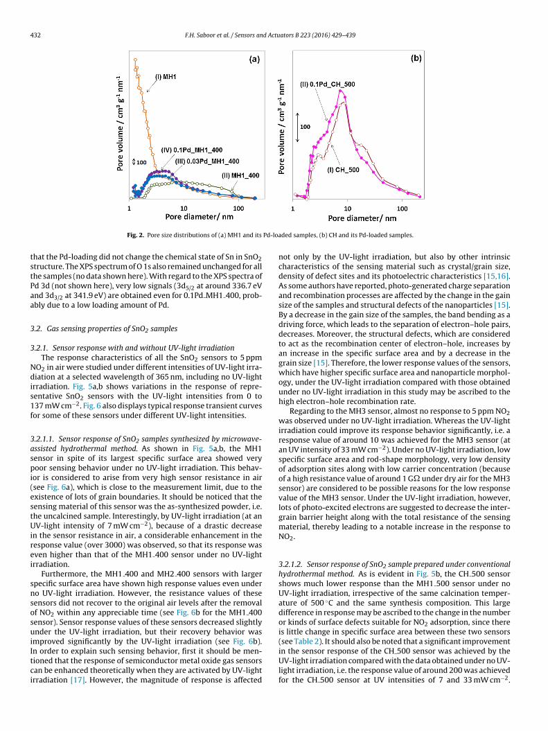
432 F.H. Saboor et al. / Sensors and Actuators B 223 (2016) 429–439
Pd-loa
tstPaa
3
3
Ndis1f
3aspi(estUirei
snsosuiItci
Fig. 2. Pore size distributions of (a) MH1 and its
hat the Pd-loading did not change the chemical state of Sn in SnO2tructure. The XPS spectrum of O 1s also remained unchanged for allhe samples (no data shown here). With regard to the XPS spectra ofd 3d (not shown here), very low signals (3d5/2 at around 336.7 eVnd 3d3/2 at 341.9 eV) are obtained even for 0.1Pd MH1 400, prob-bly due to a low loading amount of Pd.
.2. Gas sensing properties of SnO2 samples
.2.1. Sensor response with and without UV-light irradiationThe response characteristics of all the SnO2 sensors to 5 ppm
O2 in air were studied under different intensities of UV-light irra-iation at a selected wavelength of 365 nm, including no UV-light
rradiation. Fig. 5a,b shows variations in the response of repre-entative SnO2 sensors with the UV-light intensities from 0 to37 mW cm−2. Fig. 6 also displays typical response transient curvesor some of these sensors under different UV-light intensities.
.2.1.1. Sensor response of SnO2 samples synthesized by microwave-ssisted hydrothermal method. As shown in Fig. 5a,b, the MH1ensor in spite of its largest specific surface area showed veryoor sensing behavior under no UV-light irradiation. This behav-
or is considered to arise from very high sensor resistance in airsee Fig. 6a), which is close to the measurement limit, due to thexistence of lots of grain boundaries. It should be noticed that theensing material of this sensor was the as-synthesized powder, i.e.he uncalcined sample. Interestingly, by UV-light irradiation (at anV-light intensity of 7 mW cm−2), because of a drastic decrease
n the sensor resistance in air, a considerable enhancement in theesponse value (over 3000) was observed, so that its response wasven higher than that of the MH1 400 sensor under no UV-lightrradiation.
Furthermore, the MH1 400 and MH2 400 sensors with largerpecific surface area have shown high response values even undero UV-light irradiation. However, the resistance values of theseensors did not recover to the original air levels after the removalf NO2 within any appreciable time (see Fig. 6b for the MH1 400ensor). Sensor response values of these sensors decreased slightlynder the UV-light irradiation, but their recovery behavior was
mproved significantly by the UV-light irradiation (see Fig. 6b).
n order to explain such sensing behavior, first it should be men-ioned that the response of semiconductor metal oxide gas sensorsan be enhanced theoretically when they are activated by UV-lightrradiation [17]. However, the magnitude of response is affectedded samples, (b) CH and its Pd-loaded samples.
not only by the UV-light irradiation, but also by other intrinsiccharacteristics of the sensing material such as crystal/grain size,density of defect sites and its photoelectric characteristics [15,16].As some authors have reported, photo-generated charge separationand recombination processes are affected by the change in the gainsize of the samples and structural defects of the nanoparticles [15].By a decrease in the gain size of the samples, the band bending as adriving force, which leads to the separation of electron–hole pairs,decreases. Moreover, the structural defects, which are consideredto act as the recombination center of electron–hole, increases byan increase in the specific surface area and by a decrease in thegrain size [15]. Therefore, the lower response values of the sensors,which have higher specific surface area and nanoparticle morphol-ogy, under the UV-light irradiation compared with those obtainedunder no UV-light irradiation in this study may be ascribed to thehigh electron–hole recombination rate.
Regarding to the MH3 sensor, almost no response to 5 ppm NO2was observed under no UV-light irradiation. Whereas the UV-lightirradiation could improve its response behavior significantly, i.e. aresponse value of around 10 was achieved for the MH3 sensor (atan UV intensity of 33 mW cm−2). Under no UV-light irradiation, lowspecific surface area and rod-shape morphology, very low densityof adsorption sites along with low carrier concentration (becauseof a high resistance value of around 1 G� under dry air for the MH3sensor) are considered to be possible reasons for the low responsevalue of the MH3 sensor. Under the UV-light irradiation, however,lots of photo-excited electrons are suggested to decrease the inter-grain barrier height along with the total resistance of the sensingmaterial, thereby leading to a notable increase in the response toNO2.
3.2.1.2. Sensor response of SnO2 sample prepared under conventionalhydrothermal method. As is evident in Fig. 5b, the CH 500 sensorshows much lower response than the MH1 500 sensor under noUV-light irradiation, irrespective of the same calcination temper-ature of 500 ◦C and the same synthesis composition. This largedifference in response may be ascribed to the change in the numberor kinds of surface defects suitable for NO2 adsorption, since thereis little change in specific surface area between these two sensors(see Table 2). It should also be noted that a significant improvement
in the sensor response of the CH 500 sensor was achieved by theUV-light irradiation compared with the data obtained under no UV-light irradiation, i.e. the response value of around 200 was achievedfor the CH 500 sensor at UV intensities of 7 and 33 mW cm−2.
F.H. Saboor et al. / Sensors and Actuators B 223 (2016) 429–439 433
Fig. 3. FE-SEM or SEM photographs of (a) MH1, (b) MH1 400, (c) 0.03Pd MH1 400, (d) 0.1Pd MH1 400, (e) MH1 500, (f) MH2 400, (g) MH3, (h) CH 500 and (i) 0.1Pd CH 500samples.

434 F.H. Saboor et al. / Sensors and Actu
F0
SiasU
[(
Fi
ig. 4. XPS spectra of Sn 3d of (a) MH1, (b) MH1 400, (c) 0.03Pd MH1 400 and (d).1Pd MH1 400 samples.
imilar to the MH3 sensor, very low response under no UV-lightrradiation can be ascribed to very low density of adsorption siteslong with low carrier concentration. Actually the CH 500 sensorhowed a high resistance of around 0.1 G� in dry air under no
V-light irradiation.By calculating the energy per photon of irradiated UV-lightE = hc/�, in which E is energy in eV, h is Planck’s constant6.626 × 10−34 J s), c is the speed of light (2.998 × 10⁸ m s−1) and
ig. 5. (a) Variations in the sensor response of representative SnO2 sensors to 5 ppm NO2
rradiation.
Fig. 6. Response transients of (a) MH1 and (b) MH1 400 sens
ators B 223 (2016) 429–439
� is wavelength in �m; hc in terms of eV is equal to 1.24 eV-�m],365 nm wavelength corresponds to a photon energy of 3.4 eV whichis comparable with the band gap of tin dioxide (3.54–3.6 eV). Asshown in Fig. 6, when SnO2 sensors were irradiated with the UV-light the sensor resistance sharply decreased (around 2–5 ordersof magnitude). Therefore, a considerable percentage of the illu-minated UV-light with the mentioned wavelength has sufficientenergy to produce photo-generated carriers in the SnO2 thick film.
Briefly, a closer look at the results of the response propertiesreveals that UV-light irradiation could affect both the responsevalue and the recovery time for the sensors with high resistancein air under no UV-light irradiation, while the UV-light irradiationto the sensors, which have lower resistance in air under no UV-lightirradiation, could only improve the recovery time.
3.2.2. Influence of UV-light intensity on the sensor responseAs is evident in Fig. 5a, under UV-light irradiation the sensor
response decreases with an increase in the UV-light intensity. Thisbehavior could be related to the NO formation because of the photo-dissociation of NO2 under UV-light irradiation (see Eq. (2)) [26].Based on our experiments, SnO2 sensors in the present study havenot shown any response to NO gas in both air and N2 atmospherewith and without UV-light irradiation at room temperature. As anexample, Fig. 7a shows response transients of the CH 500 sensorto 80 ppm NO balanced in air atmosphere under different UV-light
intensities. A slight increase in sensor resistance after NO gas intro-duction at every condition may be attributed to the formation ofNO2, since air was used as a balance gas. To minimize the possi-ble formation of NO2 gas, NO gas balanced with N2 was used as awith UV-light intensities irradiated and (b) their sensor responses without UV-light
ors to 5 ppm NO2 under different UV-light intensities.

F.H. Saboor et al. / Sensors and Actuators B 223 (2016) 429–439 435
Fig. 7. Response transients of (a) a CH 500 sensor to 80 ppm NO balanced in air and (b) an
F(u
sNmt2egiwiciter
N
3U
abeoa
ig. 8. Variations in both the sensor resistance in air and the NO2 response of sensorsat a UV-light intensity of 33 mW cm−2) fabricated from the samples synthesizednder microwave-assisted hydrothermal with specific surface area of the samples.
ample gas. Response transients of the MH1 400 sensor to 80 ppmO gas balanced with N2 atmosphere are shown in Fig. 7b. In thiseasurement, at first the sensor is exposed to dry air for 5 min,
hen the atmosphere was changed to NO gas balanced with N2 for5 min and finally it was changed to dry air to observe its recov-ry behavior. A slight decrease in sensor resistance after the NOas introduction especially under the UV-light irradiation shownn Fig. 7b is probably due to desorption of chemisorbed oxygen
hich may be accelerated by the UV-light irradiation. Thereby, its considered that NO itself does not induce any sensor resistancehanges with and without the UV-light irradiation. Therefore by thencrease in the UV-light intensity, the following equilibrium reac-ion likely shifts to the right direction and a large amount of NO isxpected to form at high UV intensities, leading to a decrease in theesponse to NO2.
O2 + h�(� < 410 nm) � NO + 1/2O2 (2)
.2.3. Influence of specific surface area on sensor response underV-light irradiation
In this study we synthesized SnO2 samples via the microwave-ssisted hydrothermal method with different specific surface area
y changing the calcination temperature and the synthesis param-ters. As is shown in Fig. 8, the response of SnO2 sensors dependsn the specific surface area; the MH1 400 sensor has larger surfacerea and higher response as compared to those of the MH1 500MH1 400 sensor to 80 ppm NO balanced in N2 under different UV-light intensities.
sensor. Interestingly, the trend of the responses for these samplesunder UV-light irradiation remains similar to those observed underno UV-light irradiation (see Fig. 5). On the other hand, the MH2 400sensor with larger specific surface area showed lower responsethan the MH1 400 sensor. The effect of specific surface area couldbe discussed by the following two aspects: firstly, an increase inNO2 adsorption sites (via increase in the defect quantity) and sec-ondly, an increase in bulk density of the charge carries (supportedby a decrease in sensor resistance in air as shown in Fig. 8). In thisway, the sensor with low specific surface area and very low bulkdensity of the charge carries (MH1 500 sensor) likely shows lowerresponse. Additionally, the possible reason for the low response ofthe sensor having too low sensor resistance in air (MH2 400 sen-sor) is considered to arise from less pronounced change in Rg/Ra,due to an extremely large number of electrons in the bulk in air. Inother words, as a decrease in the sensor resistance in air is largerthan an increase in specific surface area (adsorption site numbersfor NO2−), the response is expected to become small. Thus, thereis an optimum specific surface area in which these two aspects actin such manner to lead to the highest gas response. Moreover, itshould be noted that due to utilizing different preparation condi-tions (different precursor types) it could also be possible to consideranother parameter (along with the effect of specific surface area andthe sensor resistance in air) affecting the nature and number of theadsorption sites of the crystalline structure of SnO2 sensors that isour future research subject to study more detailed on the effect ofprecursor types on the sensor response.
3.2.4. NO2 gas sensing mechanismBased on the results presented so far, the following mecha-
nism for NO2 sensing under UV-light irradiation can be proposed.Generally speaking, the surface of SnO2 has already been coveredwith several oxygen adsorbates such as O2−, O− and O2− in airand then a space charge layer is formed near the surface of SnO2particles. Without UV-light irradiation, only O2
− can react at tem-peratures less than 100 ◦C [27–29]. However, upon the UV-lightirradiation, all oxygen adsorbates may be accelerated. In addition,electron–hole pairs are generated and separated under the built-inelectric field near the surface of SnO2 nanoparticles [29–31]. Someof these photo-generated carries will recombine with each other.On the other hand, the increase in the number of carriers by theUV-light irradiation results in a decrease in the sensor resistancein air. Moreover, based on the literature [30,32], another possible
reason for a decrease in the sensor resistance under UV-light irradi-ation could be related to desorption of oxygen adsorbates from thesurface due to the interaction of some of photo-induced holes withthe adsorbed oxygen ions on the surface. Upon exposure to NO2
436 F.H. Saboor et al. / Sensors and Actuators B 223 (2016) 429–439
F 2 at r0
aaii
N
N
wfiir(ga
3
atssibrhtshas0Usiessr0r
rf
ig. 9. Comparison of response of bare and Pa-loaded SnO2 sensors to 5 ppm NO.1Pd MH1 400, (b) CH 500 and 0.1Pd CH 500 sensors.
s an oxidizing agent, NO2 molecules then pick up more electronsnd react with the adsorbed oxygen ions according to the follow-ng reactions, and thereby the resistance of the sensing materialncreases [33,34]:
O2(g) + e−(h�) → NO−2(ads) (3)
O2(g) + O−2(ads) + 2e− → NO−
2(ads) + 2O−(ads) (4)
Conversely, the resistance of the SnO2 sensors will decreasehen NO2 is switched to air and the NO2
− species will be desorbedrom the surface [22]. Based on this mechanism, the substantialmprovement in the response of the MH1 sensor at an UV-lightntensity of 7 mW cm−2 may be attributed to the decrease in sensoresistance in air to an appropriate level by the UV-light irradiationsee Fig. 6a) and then to the effective participation of larger photo-enerated electrons in the surface reactions expressed by Eqs. (3)nd (4).
.3. Influence of Pd-loading on gas sensing performance
We also investigated the response of the SnO2 sensors withnd without Pd-loading (0.03 and 0.1 wt%) to 5 ppm NO2 at roomemperature at different UV-light intensities. As MH1 400 sensorhowed the higher sensing response compared with the other SnO2amples synthesized by the assistance of the microwave irradiation,t was selected to study the influence of Pd-loading on its sensingehavior. The effect of palladium addition was also evaluated on theesponse of CH 500 sensor as a sample prepared by a conventionalydrothermal method. It should be noted that we were not aimingo compare these two samples with together which have differentynthesis conditions. Fig. 9a reveals that the UV-light irradiationas improved immensely the response of the 0.03Pd MH1 400nd 0.1Pd MH1 400 sensors compared with the MH1 400 sen-or at specific UV-light intensities, i.e. the response value of the.03Pd MH1 400 sensor has been enhanced about 1.6 times at anV-light intensity of 7 mW cm−2 and for the 0.1Pd MH1 400 sen-
or the response increased around 1.3, 1.3 and 11 times at UV-lightntensities of 7, 33 and 79 mW cm−2, respectively. In addition, as isvident in Fig. 9a, without UV-light irradiation two Pd-loaded MH1ensors show too low response to NO2 compared with the MH1ensor. Again, such behavior is considered to arise from very highesistance of the Pd-loaded SnO2 sensors in air (around 0.1 and.3 G� for the 0.03Pd MH1 400 and the 0.1Pd MH1 400 sensors,
espectively).On the other hand, the Pd-loading resulted in a decrease inesponse at higher UV-light intensities; higher than 33 mW cm−2
or the 0.03Pd MH1 400 sensor, but only at 137 mW cm−2 for the
oom temperature under different UV-light intensities; (a) MH1 400, 0.03Pd and
0.1Pd MH1 400 sensor. The reason for this phenomenon is not clearat present, but this may arise from UV-assisted NO2 decompositionto NO on highly dispersed Pd nanoparticles especially at high UV-light intensities. This is of course our future subject to be clarified.
Moreover Fig. 9b shows a substantial enhancement in theresponse of the 0.1Pd CH 500 sensor of about 8.5, 2.6 and 1.1 timesas compared with the response of the CH 500 sensor at UV-lightintensities of 7, 33 and 79 mW cm−2, respectively.
Briefly, the obtained results indicate that addition of palladiumcould result in an improvement in the sensor response by adjustingthe UV-light intensity for both SnO2 samples synthesized underdifferent conditions.
Fig. 10a–c also shows typical response transients of bare andPd-loaded MH1 400 and CH 500 sensors under different UV-lightintensities. As a general trend, Pd-loading gives a rise in the sen-sor resistance in air. This phenomenon can be explained by theextracting electrons from SnO2 to Pd due to the larger valueof the Pd work function (around 5.2 eV) [35] than the electronaffinity of SnO2 (around 4.5–4.8 eV) [36,37]. This electron trans-fer to Pd is accelerated if the surface of Pd is partially oxidizedin air [38].
The response enhancement by the Pd-loading could be ascribedto the role of Pd in facilitating the sensing reactions via producingadditional adsorption sites for NO2 adsorption [39]. Consequently,the number of electrons transferred to chemisorbed NO2 and themagnitude of the resistance change increases. Moreover, someauthors also reported that NO2 is more easily adsorbed on Pd andthen is spilled over to the SnO2 surface [19,40–43].
Fig. 11 shows the recovery times (trec) for some bare and Pd-loaded SnO2 sensors which were synthesized by the assistanceof microwave irradiation. As is evident from Fig. 11, trec of theMH1 400 sensor was improved by the Pd-loading at specific UV-light intensities. More precisely speaking, for the 0.1Pd MH1 400sensor trec reduced from 72 to 27 s at an UV-light intensityof 79 mW cm−2 and that of the 0.03Pd MH1 400 sensor slightlyreduced from 84 to 60 s at an UV-light intensity of 7 mW cm−2.Also, trec at an UV-light intensity of 137 mW cm−2 decreased from6 to 5 min and 3.7 min for the 0.03Pd MH1 and the 0.1Pd MH1 400sensors, respectively. Moreover, regarding to the MH1 sensor, thetrec significantly reduced from 84 to 48 s at an UV-light intensityof 7 mW cm−2 and from 6 to 1.7 min under an UV-light intensity of137 mW cm−2.
The obtained results clearly indicate that the Pd-loading as well
as utilizing the as-synthesized SnO2 powder for the sensor fabrica-tion could reduce the recovery time of sensors at specific UV-lightintensities. The reason for such behavior is not clear at present andthen is our future research subject.
F.H. Saboor et al. / Sensors and Actuators B 223 (2016) 429–439 437
Fig. 10. Typical response transients of bare and Pd-loaded SnO2 sensors; (a) MH1 400, −2
MH1 400 and 0.1Pd MH1 400 at UV-light intensities of 33 and 79 mW cm−2, (c) CH 500 a
FU
sPi
ig. 11. Recovery time for some bare and Pd-loaded SnO2 sensors under differentV-light intensities.
On the other hand, as is evident from the response transientshown in Figs. 6 and 10, the response time was prolonged by thed-loading for both MH1 400-based and CH 500-based sensors. Ass shown in Fig. 2, the Pd-loading caused a change in pore size
0.03Pd MH1 400 and 0.1Pd MH1 400 at an UV-light intensity of 7 mW cm , (b)nd 0.1Pd CH 500 sensors at UV-light intensities of 7 and 33 mW cm−2.
distribution of the MH1 400 and the CH 500 sensors, i.e. the vol-ume of pores larger than 10 nm decreased, but the volume of poressmaller than 6 nm increased by the Pd-loading. Such a changeundoubtedly hinders the facile diffusion of NO2 molecules throughthe thick film sensors from the surface to the bottom. Similarly, theslower diffusion of NO2 through the SnO2 thick film in the case ofthe MH1 sensor, due to its higher specific surface area and largevolume of pores smaller than 5 nm, could result in longer responsetime as compared with that of the MH1 400 sensor. In this regard,the change in the Pd-loading method may induce better Pd disper-sion on the SnO2 surface, leading to shorter response time of thePd-loaded sensors.
As was discussed above, the results presented indicate that thePd-loading on SnO2 sensors causes a significant improvement inUV-assisted NO2 response and shortening of the recovery time atroom temperature. Moreover, compared with NO2 response val-ues reported for various kinds of semiconductor thick film sensors[18–20,23,33,44–50] (see Table 3), the obtained results in this studyclearly shows that a combination of the loading of a small amountof Pd on SnO2 and UV-light irradiation (365 nm, 7 mW cm−2) is aneffective approach to fabricate a NO2 gas sensor capable of detec-
ting in a ppm level at room temperature with excellent responseand improved recovery time.Another important factor to be considered is an effect of rel-ative humidity on the NO2 response properties. We believe that

438 F.H. Saboor et al. / Sensors and Actuators B 223 (2016) 429–439
Table 3Comparison of the NO2 response of the best sensors reported in this study with those reported for various kinds of semiconductor gas sensors in the literature.
Sensing material Morphology Operatingtemperature (◦C)
Response(Rg/Ra)
Detectionconcentration (ppm)
UV-lightwavelength (nm)
Refs.
MH1 Nanoparticle RTa 3000 5 365 This study0.1Pd MH1 400 Nanoparticle RTa 1655 5 365 This studyAu–ZnO Nanosheet RTa 4.55 5 365 [18]Pd–ZnS Nanorod RTa 15.1 5 254 [19]Au–ZnS Nanowire 300a 8.84 5 254 [20]Bi2O3/ZnO Core/shell RTa 6.65 5 254 [23]WO3–SnO2 Nanocomposite 200b 186 200 – [33]Au–SnO2 Nanowire 300 b 30 30 – [44]Pd–SnO2 Nanowire 300 b 800 10 – [45]Pt–SnO2 Nanowire 300b 650 10 – [45]Pd–TiO2 Nanofiber 180b 37 2 – [46]Pd–ZnO/SnO2 Composite 200b 70 500 – [47]ZnO Hierarchical
nanostructureRTb 32 20 – [48]
Bi2O3 Nanowire RTb 18 100 – [49]SnO Hollow sphere 160b 2470 50 – [50]
tmbUbIo
4
sUFtc01scststtnit
cS6faei
Nstcdini
[
[
[
[
[
[
[
2
a Room temperature (RT) and UV-assisted gas sensor.b Heat-assisted gas ssensor.
he interference from the change in relative humidity in theeasurement atmosphere to the NO2 response cannot be negligi-
le small under no UV-light irradaition at room temperature. UnderV-light irradiation, however, physisorbed water is expected toe desorbed, leading to less cross-sensitivity of reative humidity.
nvestigation on the interference from relative humidity is of courceur important future subject.
. Conclusion
The effects of Pd-loading and specific surface area on the gasensing performance of SnO2 to 5 ppm NO2 was investigated underV-light irradiation with different intensities at room temperature.rom the viewpoint of the response value, it can be concludedhat the presence of a low amount of Pd (0.03 and 0.1 wt%)ould enhance the NO2 sensing performance. In this regard, the.1Pd MH1 400 sensor showed the largest improvement (about1 times) in NO2 response as compared with the bare SnO2 sen-or under an UV-light intensity of 79 mW cm−2. This enhancementould be related to the role of Pd nanoparticles via facilitating theensing reactions by producing additional NO2 adsorption sites onhe SnO2 surface. Moreover, the MH1 sensor, for which the as-ynthesized powder was used as the sensing material, showedhe highest response (over 3000) among the sensors tested inhe present study. This behavior could be attributed to a sig-ificant decrease in the sensor resistance in air under UV-light
rradiation, leading to a larger resistance change upon exposureo NO2.
From the viewpoint of the recovery time, the obtained resultslearly showed a decrease in the recovery time for the Pd-loadednO2 sensors under specific UV-light intensities. Reduction of about0% in the recovery time for the 0.1Pd MH1 400 sensor resulted in aast recovery within 27 s at an UV-light intensity of 79 mW cm−2. Inddition, a substantial decrease of about 72% and 40% in the recov-ry time has been observed for the MH1 sensor under UV-lightntensities of 137 and 7 mW cm−2, respectively.
With regard to the effect of the UV-light irradiation onO2 sensing properties of SnO2 sensors, this study could also
how that for the sensors with poor gas response (high resis-ance in air atmosphere) under no UV-light irradiation showed aonsiderable improvement in the response under UV-light irra-
iation, while for sensors with high response (low resistancen the air atmosphere) under no UV-light irradiation, there waso significant enhancement in the response value by UV-light
rradiation.
[
Acknowledgment
One of the authors (F. Hooriabad Saboor) would like to acknowl-edge the sabbatical leave awarded by the Ministry of ScienceResearch and Technology of the Islamic Republic of Iran. We wouldlike also to acknowledge the partial financial support of NationalIranian Gas Company (Contract No. 192076).
References
[1] A. Sharma, M. Tomar, V. Gupta, Enhanced response characteristics of SnO2
thin film based NO2 gas sensor integrated with nanoscaled metal oxideclusters, Sens. Actuators B 181 (2013) 735–742.
[2] W.P. Carey, B.R. Kowalski, Chemical piezoelectric sensor and sensor arraycharacterization, Anal. Chem. 58 (1986) 3077–3084.
[3] J.W. Fergus, Materials for high temperature electrochemical NOx gas sensors,Sens. Actuators B 121 (2007) 652–663.
[4] G. Lu, J. Xu, J. Sun, Y. Yu, Y. Zhang, F. Liu, UV-enhanced room temperature NO2
sensor using ZnO nanorods modified with SnO2 nanoparticles, Sens. ActuatorsB 162 (2012) 82–88.
[5] J.D. Prades, R.J. Díaz, F.H. Ramirez, S. Barth, A. Cirera, A.R. Rodríguez, S.Mathur, J.R. Morante, Equivalence between thermal and room temperatureUV light-modulated responses of gas sensors based on individual SnO2
nanowires, Sens. Actuators B 140 (2009) 337–341.[6] Y.J. Chen, L. Nie, X.Y. Xue, Y.G. Wang, T.H. Wang, Linear ethanol sensing of
SnO2 nanorods with extremely high sensitivity, Appl. Phys. Lett. 88 (2006)083105.
[7] S.W. Fan, A.K. Srivastava, V.P. Dravid, UV-activated room-temperature gassensing mechanism of polycrystalline ZnO, Appl. Phys. Lett. 95 (2009) 142106.
[8] X. Liu, S. Cheng, H. Liu, Sh. Hu, D. Zhang, H. Ning, A survey on gas sensingtechnology, Sensors 12 (2012) 9635–9665.
[9] K. Ihokura, J. Watson, The Stannic Oxide Gas Sensor Principles andApplications, CRC Press, Boca Raton, 1994.
10] A. Kolmakov, X.H. Chen, M. Moskovits, Functionalizing nanowires withcatalytic nanoparticles for gas sensing application, J. Nanosci. Nanotechnol. 8(2008) 111–121.
11] X. Liu, J. Zhang, T. Yang, X. Guo, S. Wu, S. Wang, Synthesis of Pt nanoparticlesfunctionalized WO3 nanorods and their gas sensing properties, Sens.Actuators B 156 (2011) 918–923.
12] Y. Zhang, A. Kolmakov, Y. Lilach, M. Moskovits, Electronic control of chemistryand catalysis at the surface of an individual tin oxide nanowire, J. Phys. Chem.B 109 (2005) 1923–1929.
13] S. Park, T. Hong, J. Jung, Ch. Lee, Room temperature hydrogen sensing ofmultiple networked ZnO/WO3 core–shell nanowire sensors under UVillumination, Curr. Appl. Phys. 14 (2014) 1171–1175.
14] E. Comini, G. Faglia, G. Sberveglieri, UV light activation of tin oxide thin filmsfor NO2 sensing at low temperatures, Sens. Actuators B 78 (2001) 73–77.
15] L. Peng, J. Zhai, D. Wang, Y. Zhang, P. Wang, Q. Zhao, T. Xie, Size- andphotoelectric characteristics-dependent formaldehyde sensitivity of ZnOirradiated with UV light, Sens. Actuators B 148 (2010) 66–73.
16] B.P.J. de Lacy Costello, R.J. Ewen, N.M. Ratcliffe, M. Richards, Highly sensitive
room temperature sensors base d on the UV-LED activation of zinc oxidenanoparticles, Sens. Actuators B 134 (2008) 945–952.17] S. Mishra, C. Ghanshyam, N. Ram, R.P. Bajpai, R.K. Bedi, Detection mechanismof metal oxide gas sensor under UV radiation, Sens. Actuators B 97 (2004)387–390.

d Actu
[
[
[
[
[
[
[
[
[
[
[
[
[
[
[
[
[
[
[
[
[
[
[
[
[
[
[
[
[
[
[
[
[
F.H. Saboor et al. / Sensors an
18] Y. Mun, S. Park, S. An, Ch. Lee, H.W. Kim, NO2 gas sensing properties ofAu-functionalized porous ZnO nanosheets enhanced by UV irradiation,Ceram. Int. 39 (2013) 8615–8622.
19] S. Park, S. An, Y. Mun, C. Lee, UV-activated gas sensing properties of ZnSnanorods functionalized with Pd, Curr. Appl. Phys. 14 (2014) S57–S62.
20] S. Park, S. An, H. Ko, S. Lee, C. Lee, Synthesis, structure, and UV-enhanced gassensing properties of Au-functionalized ZnS nanowires, Sens. Actuators B 188(2013) 1270–1276.
21] D. Haridas, A. Chowdhuri, K. Sreenivas, V. Gupta, Enhanced room temperatureresponse of SnO2 thin film sensor loaded with Pt catalyst clusters under UVradiation for LPG, Sens. Actuators B 153 (2011) 152–157.
22] K. Anothainar, M. Burgmair, A. Karthigeyan, M. Zimmer, I. Eisele, Lightenhanced NO2 gas sensing with tin oxide at room temperature: conductanceand work function measurements, Sens. Actuators B 93 (2003) 580–584.
23] S. Park, H. Ko, S. Lee, H. Kim, C. Lee, Light-activated gas sensing ofBi2O3-core/ZnO-shell nanobelt gas sensors, Thin Solid Films (2014), http://dx.doi.org/10.1016/j.tsf.2014.02.110.
24] S.G. Ansari, M.A. Dar, Y.-S. Kim, G.-S. Kim, H.-K. Seo, G. Khang, H.-S. Shin, Effectof growth temperature on the morphology and bonded states of SnO2
nanobaskets, Appl. Surf. Sci. 253 (2007) 4668–4672.25] R.-Q. Tan, Y.-Q. Guo, J.-H. Zhao, Y. Li, T.-F. Xu, W.-J. Song, Synthesis,
characterization and gas-sensing properties of Pd-doped SnO2 nanoparticles,Trans. Nonferrous Met. Soc. China 21 (2011) 1568–1573.
26] S. Madronich, in: M.-L. Chanin (Ed.), The Role of the Stratosphere in GlobalChange, NATO-ASI Series, vol. 18, Springer-Verlag, Amsterdam, 1993, pp.437–461.
27] N. Barsan, U. Weimar, Conduction model of metal oxide gas sensors, J.Electroceram. 7 (2001) 143–167.
28] N. Yamazoe, Oxide semiconductor gas sensors, Catal. Surv. Asia 7 (2003)63–75.
29] Y. Muraoka, N. Takubo, Z. Hiroi, Photoinduced conductivity in tin dioxide thinfilms, J. Appl. Phys. 105 (2009) 103702.
30] H. Chen, Y. Liu, Ch. Xie, J. Wu, D. Zeng, Y. Liao, A comparative study on UV lightactivated porous TiO2 and ZnO film sensors for gas sensing at roomtemperature, Ceram. Int. 38 (2012) 503–509.
31] C.-H. Lin, R.-S. Chen, T.-T. Chen, H.-Y. Chen, Y.-F. Chen, K.-H. Chen, L.-C. Chen,High photocurrent gain in SnO2 nanowires, Appl. Phys. Lett. 93 (2008) 112115.
32] J.D. Prades, F. Hernandez-Ramirez, R. Jimenez-Diaz, M. Manzanares, T.Andreu, A. Cirera, A. Romano-Rodriguez, J.R. Morante, The effects ofelectron–hole separation on the photoconductivity of individual metal oxidenanowires, Nanotechnology 19 (2008) 465501.
33] S. Bai, D. Li, D. Han, R. Luo, A. Chen, C.L. Chung, Preparation, characterizationof WO3–SnO2 nanocomposites and their sensing properties for NO2, Sens.Actuators B 150 (2010) 749–755.
34] A. Afzal, N. Cioffi, L. Sabbatini, L. Torsi, NOx sensors based on semiconductingmetal oxide nanostructures: progress and perspectives, Sens. Actuators B171–172 (2012) 25–42.
35] S. Halas, T. Durakiewicz, P. Mackiewicz, Temperature-dependent workfunction shifts of hydrogenated/deuteriated palladium: a new theoreticalexplanation, Surf. Sci. 555 (2004) 43–50.
36] Y. Cheng, R. Yang, J.-P. Zheng, Z.L. Wang, P. Xiong, Characterizing individualSnO2 nanobelt field-effect transistors and their intrinsic responses tohydrogen and ambient gases, Mater. Chem. Phys. 137 (2012) 372–380.
37] M.N. Islam, M.O. Hakim, Electron affinity and work function of polycrystallineSnO2 thin film, J. Mater. Sci. Lett. 5 (1986) 63–65.
38] N. Yamamoto, S. Tonomura, T. Matsuoka, H. Tsubomura, A study on apalladium–titanium oxide Schottky diode as a detector for gaseouscomponents, Surf. Sci. 92 (1980) 400–406.
39] O.V. Safonova, G. Delabouglise, B. Chenevier, A.M. Gaskov, M. Labeau, CO andNO2 gas sensitivity of nanocrystalline tin dioxide thin films doped with Pd, Ruand Rh, Mater. Sci. Eng. C 21 (2002) 105–111.
40] N.M. Shaalan, T. Yamazaki, T. Kikuta, NO2 response enhancement andanomalous behavior of n-type SnO2 nanowires functionalized by Pdnanodots, Sens. Actuators B 166–167 (2012) 671–677.
41] A. Kolmakov, D.O. Klenov, Y. Lilach, S. Stemmer, M. Moskovits, Enhanced gassensing by individual SnO2 nanowires and nanobelts functionalized with Pdcatalyst particles, Nano Lett. 5 (2005) 667–673.
42] M. Bowker, L.J. Bowker, R.A. Bennett, P. Stone, A. Ramirez-Cuesta, In
consideration of precursor states, spillover and Boudart’s ‘collection zone’ andof their role in catalytic processes, J. Mol. Catal. A 163 (2000) 221–232.43] R.L. Vander Wal, G.W. Hunter, J.C. Xu, M.J. Kulis, G.M. Berger, T.M. Ticich,Metal-oxide nanostructure and gas-sensing performance, Sens. Actuators B138 (2009) 113–119.
ators B 223 (2016) 429–439 439
44] S.-W. Choi, S.-H. Jung, S.S. Kim, Significant enhancement of the NO2 sensingcapability in networked SnO2 nanowires by Au nanoparticles synthesized via�-ray radiolysis, J. Hazard. Mater. 193 (2011) 243–248.
45] S.-W. Choi, A. Katoch, G.-J. Sun, S.S. Kim, Bimetallic Pd/Ptnanoparticle-functionalized SnO2 nanowires for fast response and recovery toNO2, Sens. Actuators B 181 (2013) 446–453.
46] J. Moon, J.-A. Park, S.-J. Lee, T. Zyung, I.-D. Kim, Pd-doped TiO2 nanofibernetworks for gas sensor applications, Sens. Actuators B 149 (2010)301–305.
47] C. Liangyuan, B. Shouli, Z. Guokun, L. Dianqing, C. Aifan, C.C. Liu, Synthesis ofZnO–SnO2 nanocomposites by microemulsion and sensing properties forNO2, Sens. Actuators B 134 (2008) 360–366.
48] X. Pan, X. Zhao, J. Chen, A. Bermak, Z. Fan, A fast-response/recovery ZnOhierarchical nanostructure based gas sensor with ultra-highroom-temperature output response, Sens. Actuators B 206 (2015) 764–771.
49] X. Gou, R. Li, G. Wang, Z. Chen, D. Wexler, Room-temperature solutionsynthesis of Bi2O3 nanowires for gas sensing application, Nanotechnology 20(2009) 495501.
50] J. Zhang, S. Wang, Y. Wang, Y. Wang, B. Zhu, H. Xia, X. Guo, S. Zhang, W.Huang, S. Wu, NO2 sensing performance of SnO2 hollow sphere sensor, Sens.Actuators B 135 (2009) 610–617.
Biographies
Fahime HooriAbad Saboor received the M.Sc. degree in chemical engineering fromIran University of Science and Technology, Tehran, Iran in 2009. She is currentlythe Ph.D. Candidate of nanotechnology at University of Tehran, Tehran, Iran. Herresearch interests include synthesis and characterization of nanostructured mate-rials as applied to chemical gas sensors, catalysis, membrane separation processesespecially zeolite type membranes.
Taro Ueda received his B.Eng. degree in materials science and M.Eng. degree in mate-rials science in 2003 and 2005, respectively, from Kyushu Institute of Technology,Japan, and Dr.Eng. degree in 2008 from Kyushu University, Japan. He has been anassistant professor at Nagasaki University since 2013. His current research interestis the development of high-performance chemical sensors and the elucidation ofgas reaction mechanism on the sensing materials.
Kai Kamada received his B.Eng., M. Eng., and D. Eng. degrees in applied chemistryin 1997, 1999, and 2003, respectively, from Kumamoto University. He has beenan associate professor at Nagasaki University since 2012. His research interestsare fabrication and functionalization of various types of inorganic-bionanohybridmaterials.
Takeo Hyodo received his B.Eng. degree in applied chemistry and M.Eng. degree inmaterials science and technology in 1992 and 1994, respectively, and Dr.Eng. degreein 1997 from Kyushu University. He has been an associate professor at NagasakiUniversity since 2010. His research interests are development of various electro-chemical devices such as chemical sensors, secondary lithium-ion batteries, anddye-sensitized solar cells, and design of the related mesoporous and macroporousmaterials.
Yadollah Mortazavi received the B.Sc. degree in chemical engineering from Uni-versity of Shiraz, Shiraz, Iran, and the M.Sc. and Ph.D., degrees in chemicalengineering from University of Waterloo, Waterloo, Canada. He joined Univer-sity of Tehran, Tehran, Iran in 1995. His research interests include catalysis andreaction engineering especially in C1 chemistry, environmental catalysis, chemicalgas-sensors and nanostructured materials. Currently he is the chair of Nano-technology Department at College of Engineering, University of Tehran, Tehran,Iran.
Abbas Ali Khodadadi received his M.Sc. in Chemical Engineering from University ofTehran, Tehran, Iran and his Ph.D. in catalysis and reaction engineering from Univer-sity of Waterloo, Waterloo, Canada, in 1994. His research interests include catalysis,reaction engineering, nanostructured materials as applied to nano-particles, car-bon nanotubes, plasma-catalytic conversion of natural gas to liquids and chemicals,metal oxide semiconductor gas-sensors, air pollution control using catalytic con-verters and oxygen sensors using solid electrolytes.
Yasuhiro Shimizu received his B.Eng. degree in applied chemistry in 1980 andDr.Eng. degree in 1987 from Kyushu University. He has been a professor at NagasakiUniversity since 2005. His current research concentrates on development of gassensors based on various kinds of sensing principles.
Related Documents


