User Manual PCA-6742 Half-Size CPU Card

Welcome message from author
This document is posted to help you gain knowledge. Please leave a comment to let me know what you think about it! Share it to your friends and learn new things together.
Transcript

User Manual
PCA-6742
Half-Size CPU Card
CopyrightThe documentation and the software included with this product are copyrighted 2013by Advantech Co., Ltd. All rights are reserved. Advantech Co., Ltd. reserves the rightto make improvements in the products described in this manual at any time withoutnotice. No part of this manual may be reproduced, copied, translated or transmittedin any form or by any means without the prior written permission of Advantech Co.,Ltd. Information provided in this manual is intended to be accurate and reliable. How-ever, Advantech Co., Ltd. assumes no responsibility for its use, nor for any infringe-ments of the rights of third parties, which may result from its use.
AcknowledgementsAward is a trademark of Award Software International, Inc.
VIA is a trademark of VIA Technologies, Inc.
IBM, PC/AT, PS/2 and VGA are trademarks of International Business Machines Cor-poration.
Intel and Pentium are trademarks of Intel Corporation.
Microsoft Windows® is a registered trademark of Microsoft Corp.
RTL is a trademark of Realtek Semi-Conductor Co., Ltd.
ESS is a trademark of ESS Technology, Inc.
UMC is a trademark of United Microelectronics Corporation.
SMI is a trademark of Silicon Motion, Inc.
Creative is a trademark of Creative Technology LTD.
All other product names or trademarks are properties of their respective owners.
For more information on this and other Advantech products, please visit our websitesat: http://www.advantech.com
http://www.advantech.com/eplatform
For technical support and service, please visit our support website at: http://www.advantech.com/support
This manual is for the PCA-6742.
Part No. 2002674201 Edition 2
Printed in China May 2013
PCA-6742 User Manual ii
Product Warranty (2 years)Advantech warrants to you, the original purchaser, that each of its products will befree from defects in materials and workmanship for two years from the date of pur-chase.
This warranty does not apply to any products which have been repaired or altered bypersons other than repair personnel authorized by Advantech, or which have beensubject to misuse, abuse, accident or improper installation. Advantech assumes noliability under the terms of this warranty as a consequence of such events.
Because of Advantech’s high quality-control standards and rigorous testing, most ofour customers never need to use our repair service. If an Advantech product is defec-tive, it will be repaired or replaced at no charge during the warranty period. For out-of-warranty repairs, you will be billed according to the cost of replacement materials,service time and freight. Please consult your dealer for more details.
If you think you have a defective product, follow these steps:
1. Collect all the information about the problem encountered. (For example, CPU speed, Advantech products used, other hardware and software used, etc.) Note anything abnormal and list any onscreen messages you get when the problem occurs.
2. Call your dealer and describe the problem. Please have your manual, product, and any helpful information readily available.
3. If your product is diagnosed as defective, obtain an RMA (return merchandise authorization) number from your dealer. This allows us to process your return more quickly.
4. Carefully pack the defective product, a fully-completed Repair and Replacement Order Card and a photocopy proof of purchase date (such as your sales receipt) in a shippable container. A product returned without proof of the purchase date is not eligible for warranty service.
5. Write the RMA number visibly on the outside of the package and ship it prepaid to your dealer.
Declaration of Conformity
FCC Class A
Note: This equipment has been tested and found to comply with the limits for a ClassA digital device, pursuant to part 15 of the FCC Rules. These limits are designed toprovide reasonable protection against harmful interference when the equipment isoperated in a commercial environment. This equipment generates, uses, and canradiate radio frequency energy and, if not installed and used in accordance with theinstruction manual, may cause harmful interference to radio communications. Opera-tion of this equipment in a residential area is likely to cause harmful interference inwhich case the user will be required to correct the interference at his own expense.
Caution! There is a danger of a new battery exploding if it is incorrectly installed. Do not attempt to recharge, force open, or heat the battery. Replace the battery only with the same or equivalent type recommended by the man-ufacturer. Discard used batteries according to the manufacturer's instructions.
iii PCA-6742 User Manual
Technical Support and Assistance1. Visit the Advantech web site at www.advantech.com/support where you can find
the latest information about the product.2. Contact your distributor, sales representative, or Advantech's customer service
center for technical support if you need additional assistance. Please have the following information ready before you call:– Product name and serial number– Description of your peripheral attachments– Description of your software (operating system, version, application software,
etc.)– A complete description of the problem– The exact wording of any error messages
Packing ListBefore setting up the system, check that the items listed below are included and ingood condition. If any item does not accord with the table, please contact your dealerimmediately.
1 PCA-6742 Series Half-size CPU Card 1 keyboard / PS2 mouse cable p/n:1700060202 1 COM2 + parallel port cable p/n:1701260305 1 USB cable with 4 ports (2.0mm pitch) p/n:1700008887 1 Jumper pack p/n:9689000002 1 Warranty Certificate
If any of these items are missing or damaged, contact your distributor or sales repre-sentative immediately.
PCA-6742 User Manual iv
Contents
Chapter 1 General Information ............................11.1 Introduction ............................................................................................... 21.2 Specifications ............................................................................................ 2
1.2.1 Standard System On Module Functions ....................................... 21.2.2 VGA/Flat Panel Interface .............................................................. 21.2.3 Audio Function .............................................................................. 2
1.3 Mechanical and Environmental ................................................................. 2
Chapter 2 Connecting Peripherals ......................32.1 Jumper and Connector Locations ............................................................. 4
Figure 2.1 Jumper and Connector Locations (Component Side) 4Figure 2.2 Jumper and Connector Locations (Solder Side)......... 4
2.2 Jumpers and Connectors .......................................................................... 5Table 2.1: Jumpers...................................................................... 5Table 2.2: Connectors ................................................................. 5
2.3 Setting Jumpers ........................................................................................ 62.3.1 Setting Details............................................................................... 6
2.4 Front Panel Connectors (JFP1 & JFP2).................................................... 82.5 IR Connector (JIR1) .................................................................................. 82.6 IDE Connector (IDE1) ............................................................................... 82.7 CompactFlash Card Socket (CF1) ............................................................ 82.8 Parallel Port Connector (LPT1) ................................................................. 92.9 USB Ports (USB12 & USB34)................................................................... 9
2.10 Serial Ports (COM1 & COM2 & COM3,4) ................................................. 92.10.1 COM2 RS-232/RS-422/RS-485 Settings ...................................... 9
2.11 PS/2 Keyboard / Mouse Connector (KBMS1 & 2)..................................... 92.12 VGA Connector (VGA1) ............................................................................ 92.13 Ethernet Connector (LAN1)..................................................................... 10
2.13.1 Network Boot .............................................................................. 102.14 Front Panel LAN Indicate Connector (LANLED1) ................................... 102.15 System FAN Connector (SYSFAN1)....................................................... 102.16 AT Power Connector (PWR1) ................................................................. 102.17 GPIO Header (GPIO1) ............................................................................ 102.18 Flat Panel Display Connector (LCD1 & LVDS1) ..................................... 10
2.18.1 TTL TFT LCD Connector (LCD1)................................................ 102.18.2 LVDS TFT LCD Connector (LVDS1) (Optional).......................... 10
2.19 PC/104 Connector (PC104) .................................................................... 10
Chapter 3 BIOS Operation..................................113.1 BIOS Introduction.................................................................................... 123.2 BIOS Setup ............................................................................................. 12
3.2.1 Main Menu .................................................................................. 133.2.2 Standard CMOS Features .......................................................... 143.2.3 Advanced BIOS Features ........................................................... 153.2.4 Advanced Chipset Features........................................................ 163.2.5 Integrated Peripherals................................................................. 173.2.6 PnP/PCI Configurations .............................................................. 193.2.7 Load Optimized Defaults............................................................. 193.2.8 Set Password.............................................................................. 203.2.9 Quit Without Saving .................................................................... 21
v PCA-6742 User Manual

Appendix A Pin Assignments............................... 23A.1 Front Panel Connectors (JFP1) .............................................................. 24
Table A.1: Front Panel Connectors (JFP1)................................ 24A.2 Front Panel Connectors (JFP2) .............................................................. 24
Table A.2: Front Panel Connectors (JFP2)................................ 24A.3 USB Ports (USB12 & USB34)................................................................. 25
Table A.3: USB Ports (USB12 & USB34) .................................. 25A.4 Serial Ports (COM2)................................................................................ 25
Table A.4: Serial Ports (COM2) ................................................. 25A.5 Serial Ports (COM34).............................................................................. 26
Table A.5: Serial Ports (COM34) ............................................... 26A.6 PS/2 Keyboard / Mouse Connector (KBMS2)......................................... 26
Table A.6: PS/2 Keyboard / Mouse Connector (KBMS2) .......... 26A.7 Front Panel LAN Indicate Connector (LANLED1)................................... 27
Table A.7: Front Panel LAN Indicate Connector (LANLED1) .... 27A.8 System FAN Connector (SYSFAN1) ...................................................... 27
Table A.8: System FAN Connector (SYSFAN1)........................ 27A.9 GPIO Header (GPIO1)............................................................................ 28
Table A.9: GPIO Header (GPIO1) ............................................. 28A.10 TTL TFT LCD Connector (LCD1)............................................................ 28
Table A.10:TTL TFT LCD Connector (LCD1) ............................. 28A.11 LVDS TFT LCD Connector (LVDS1) ...................................................... 29
Table A.11:LVDS TFT LCD Connector (LVDS1)........................ 29A.12 Inverter power Connector (INV1) ............................................................ 29
Table A.12:Inverter Power Connector (INV1) ............................. 29
Appendix B Programming the Watchdog Timer . 31B.1 Introduction ............................................................................................. 32
B.1.1 Watchdog Timer Overview ......................................................... 32Table B.1: Watchdog Timer Registers....................................... 34
B.1.2 Example Program....................................................................... 34
Appendix C System Assignments........................ 39C.1 System I/O Ports..................................................................................... 40
Table C.1: System I/O Ports ...................................................... 40C.2 DMA Channel Assignments .................................................................... 40
Table C.2: DMA Channel Assignments ..................................... 40C.3 Interrupt Assignments ............................................................................. 41
Table C.3: Interrupt Assignments .............................................. 41C.4 1st MB Memory Map............................................................................... 41
Table C.4: 1st MB Memory Map ................................................ 41
Appendix D Installing PC/104 Modules................ 43D.1 Introduction ............................................................................................. 44
Figure D.1 PC/104 Module Mounting Diagram .......................... 44Figure D.2 PC/104 Module Dimensions (mm) (± 0.1) ................ 45
Appendix E Mechanical Drawings ....................... 47
PCA-6742 User Manual vi
Chapter 1
1 General InformationThis chapter gives background information on the PCA-6742 Half-Size CPU Card.
1.1 IntroductionThe PCA-6742 is the ultimate cost-effective solution for limited space applications. Itoffers all the functions of an AT-compatible industrial computer on a single board. Thenew CPU module supports Advantech EVA-X4300 SOC (system on chip) which sup-ports ISA interfaces.
On-board features include a 10/100 Ethernet interface, Compact Flash socket (TypeI/II) shared with secondary IDE, Enhanced IDE interface, one parallel port, four serialports (1 x RS-232 on rear I/O, 2 x RS-232, 1 x RS-232/422/485), and a PS/2 key-board/mouse interface. An SVGA/LCD display controller (LCD and CRT displays)allows LCD screen resolutions up to 1024 x 768 @ 18/24 bit LVDS/TTL (Optional)and CRT resolutions up to 1024 x 768 @ 24 bit true color.
The PCA-6742 complies with the "Green Function" standard and supports threetypes of power saving features: Normal, Doze and Sleep modes.
If you need any additional functions, the PCA-6742 has a PC/104 connector forfuture upgrades.
1.2 Specifications
1.2.1 Standard System On Module Functions CPU: Advantech SOC EVA-X4300 300MHz BIOS: Advantech SOC EVA-X4300 300MHz integrated BIOS Chipset: Advantech SOC EVA-X4300 System memory: Onboard 64 / 128 (Optional) MB DDR2 Memory Enhanced IDE interface: 1 EIDE channel for two devices. BIOS auto-detect up
to UDMA -100 Watchdog timer: 255 level timer interval, setup by software or
Jumper less selection generates system reset or IRQ11.
USB interface: Support 4 ports USB 2.0 (USB1.1 under DOS) Expansion Interface: Supports ISA interface
1.2.2 VGA/Flat Panel Interface Chipset: VGA mode: SM712 graphic chip LCD mode: SMI SM712 2D graphic chip Memory Size: 4 MB display memory Display mode: VGA mode supports 1024 x 768 @ 24-bit true color
LCD mod supports 1024 x 768 @ 18/24-bit TTL / LVDS (Optional) TFT panel.
1.2.3 Audio Function Audio interface: N/A
1.3 Mechanical and EnvironmentalDimensions: 185 mm (L) x 122 mm (W) (7.3" x 4.8")
Power supply voltage: Typical: +5V @ 1.6 A
Power requirement: Max: +5V @ 2 A
Operating temperature: 0 ~ 60°C (32 ~ 140° F)
Operating humidity: 0% ~ 90% relative humidity, non-condensing
Weight: 0.185 Kg (0.4 lbs)
PCA-6742 User Manual 2

Chapter 2
2 Connecting PeripheralsThis chapter tells how to connect peripherals, switches and indica-tors to the PCA-6742 board. You can access most of the connec-tors from the top of the board while it is installed in the chassis. If you have a number of cards installed, or your chassis is very tight, you may need to partially remove the card to make all the connections.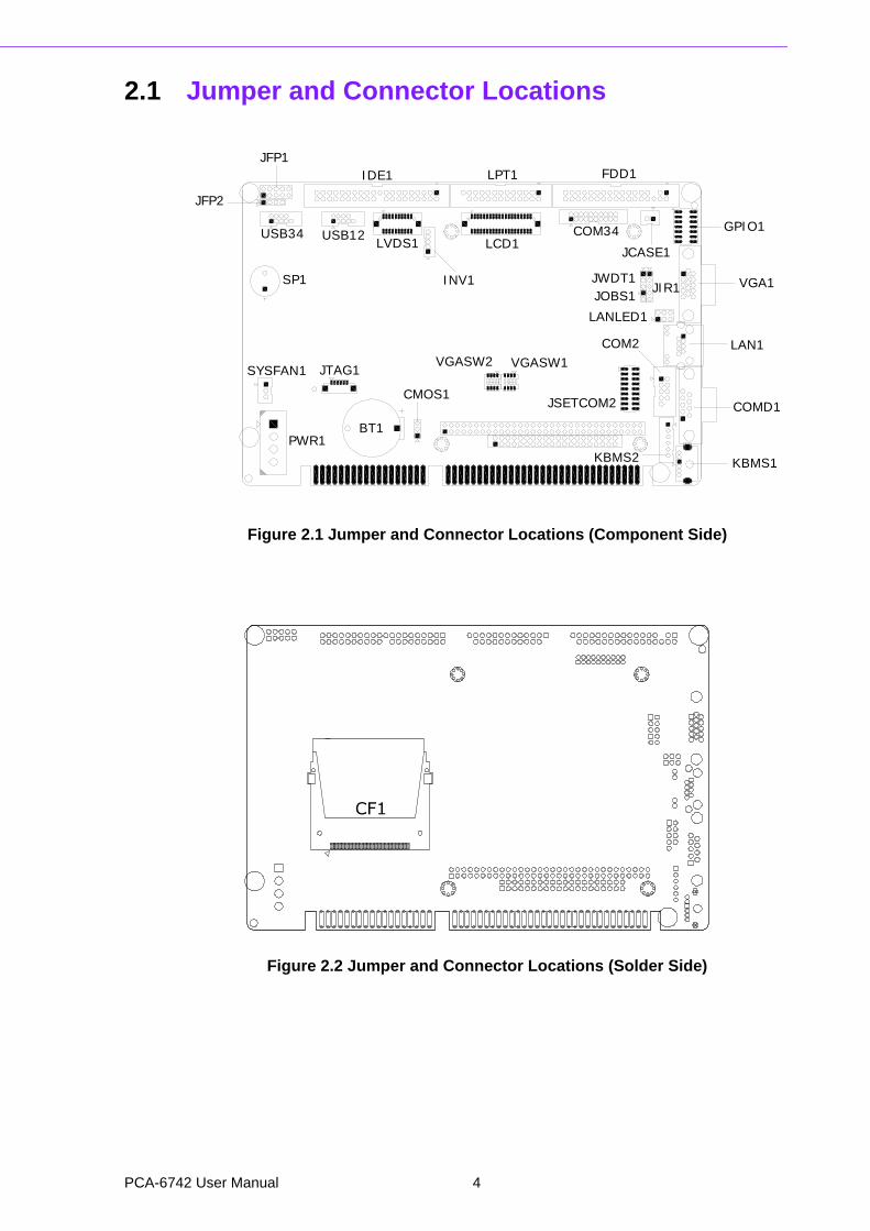
2.1 Jumper and Connector Locations
Figure 2.1 Jumper and Connector Locations (Component Side)
Figure 2.2 Jumper and Connector Locations (Solder Side)
USB34 USB12
JFP1
JFP2
SP1
LVDS1
IDE1
INV1
LCD1
LPT1
JTAG1
BT1
CMOS1
SYSFAN1
PWR1
VGASW1VGASW2
JSETCOM2
COM34JCASE1
FDD1
GPIO1
VGA1JWDT1JOBS1 JIR1
LANLED1
LAN1COM2
COMD1
KBMS1KBMS2
PCA-6742 User Manual 4
Chapter 2
Connecting
Peripherals
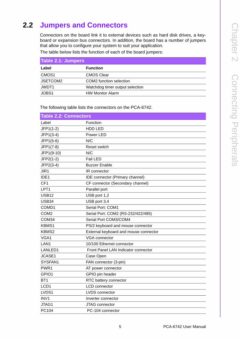
2.2 Jumpers and ConnectorsConnectors on the board link it to external devices such as hard disk drives, a key-board or expansion bus connectors. In addition, the board has a number of jumpersthat allow you to configure your system to suit your application.
The table below lists the function of each of the board jumpers:
The following table lists the connectors on the PCA-6742.
Table 2.1: Jumpers
Label Function
CMOS1 CMOS Clear
JSETCOM2 COM2 function selection
JWDT1 Watchdog timer output selection
JOBS1 HW Monitor Alarm
Table 2.2: ConnectorsLabel Function
JFP1(1-2) HDD LED
JFP1(3-4) Power LED
JFP1(5-6) N/C
JFP1(7-8) Reset switch
JFP1(9-10) N/C
JFP2(1-2) Fail LED
JFP2(3-4) Buzzer Enable
JIR1 IR connector
IDE1 IDE connector (Primary channel)
CF1 CF connector (Secondary channel)
LPT1 Parallel port
USB12 USB port 1,2
USB34 USB port 3,4
COMD1 Serial Port: COM1
COM2 Serial Port: COM2 (RS-232/422/485)
COM34 Serial Port COM3/COM4
KBMS1 PS/2 keyboard and mouse connector
KBMS2 External keyboard and mouse connector
VGA1 VGA connector
LAN1 10/100 Ethernet connector
LANLED1 Front Panel LAN Indicator connector
JCASE1 Case Open
SYSFAN1 FAN connector (3-pin)
PWR1 AT power connector
GPIO1 GPIO pin header
BT1 RTC battery connector
LCD1 LCD connector
LVDS1 LVDS connector
INV1 Inverter connector
JTAG1 JTAG connector
PC104 PC-104 connector
5 PCA-6742 User Manual

2.3 Setting JumpersYou may configure your card to match the needs of your application by setting jump-ers. A jumper is the simplest kind of electrical switch. It consists of two metal pins anda small metal clip (often protected by a plastic cover) that slides over the pins to con-nect them. To "close" a jumper, you connect the pins with the clip. To "open” ajumper you remove the clip. Sometimes a jumper will have three pins, labeled 1, 2,and 3. In this case you would connect either pins 1 and 2 or 2 and 3.
The jumper settings are schematically depicted in this manual as follows:
A pair of needle-nose pliers may be helpful when working with jumpers.
If you have any doubts about the best hardware configuration for your application,contact your local distributor or sales representative before you make any changes.
Generally, you simply need a standard cable to make most connections
2.3.1 Setting Details
CMOS1 CMOSW Clear
Setting Function
1-2 Clear CMOS
2-3 Normal operation
1
PCA-6742 User Manual 6
Chapter 2
Connecting
Peripherals
JSETCOM2 COM2 Function Selection
JWDT1 Watchdog Timer Output Selection
Setting Function
1-2 IRQ11
2-3 System reset
JOBS1 HW Monitor Alarm
Setting Function
1-2 Close Enable OBS alarm
2-3 Open Disable OBS alarm
1
3
1
7 PCA-6742 User Manual
The following sections tell how to make each connection. In most cases, you will sim-ply need to connect a standard cable. All of the connector pin assignments areshown in Appendix A.
2.4 Front Panel Connectors (JFP1 & JFP2)There are several external switches to monitor and control the PCA-6742.
2.5 IR Connector (JIR1)This connector supports the optional wireless infrared transmitting and receivingmodule. This module mounts on the system case. You must configure the settingthrough BIOS setup.
2.6 IDE Connector (IDE1)The PCA-6742 provides 1 IDE channel which you can attach up to two EnhancedIntegrated Device Electronics hard disk drives or CD-ROM to the board’s internalcontroller. Its IDE controller uses a PCI interface. This advanced IDE controller sup-ports faster data transfer up to UDMA 100.
Wire number 1 on the cable is red or blue, and the other wires are gray. Connect oneend to connector CN1 on the CPU card. Make sure that the red (or blue) wire corre-sponds to pin 1 on the connector. See Figure 2-1, where pin 1 is indicated with a tri-angle and a solid square.
IDE hard drives can connect in either position on the cable. If you install two drives,you will need to set one as the master and one as the slave. You do this by settingthe jumpers on the drives. If you use just one drive, you should set it as the master.See the documentation that came with your drive for more information.
Connect the first hard drive to the other end of the cable. Wire 1 on the cable shouldalso connect to pin 1 on the hard drive connector, which should be labeled on thedrive circuit board. Check the documentation that came with the drive for more infor-mation. If you are using a second drive, connect it to the remaining connector on thesame cable.
2.7 CompactFlash Card Socket (CF1)The board provides a CompactFlash card type I/II socket. The CompactFlash cardshares a secondary IDE channel.
Warning! Always completely disconnect the power cord from your chassis when-ever you are working on it. Do not make connections while the power is on. Sensitive electronic components can be damaged by a sudden rush of power. Only experienced electronics personnel should open the PC chassis.
Caution! Always ground yourself to remove any static charge before touching the CPU card. Modern electronic devices are very sensitive to static electric charges. Use a grounding wrist strap at all times. Place all electronic components on a static-dissipative surface or in a static-shielded bag when they are not in the chassis.
PCA-6742 User Manual 8

Chapter 2
Connecting
Peripherals
2.8 Parallel Port Connector (LPT1)The parallel port is designated as LPT1, and is normally used to connect the CPUcard to a printer. The PCA-6742 includes an onboard parallel port, accessed througha 26-pin flat-cable connector. The card comes with an adapter cable which lets youuse a traditional DB-25 connector. The cable has a 26-pin connector on one end anda DB-25 connector on the other, mounted on a retaining bracket. The bracket installsat the end of an empty slot in your chassis, giving you access to the connector.
To install the bracket, find an empty slot in your chassis. Unscrew the plate that cov-ers the end of the slot. Screw in the bracket in place of the plate. Next, attach the flat-cable connector to LPT1 on the CPU card. Wire 1 of the cable is red or blue, and theother wires are gray. Make sure that wire 1 corresponds to pin 1 of LPT1. Pin 1 is onthe right side of LPT1.
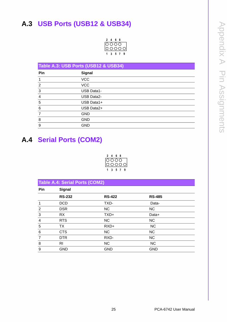
2.9 USB Ports (USB12 & USB34)The PCA-6742 provides a USB interface (up to 4 ports), which gives complete Plug &Play and hot swapping for up to 127 external devices. The USB interface complieswith USB Specification Rev. 2.0 and Rev. 1.1 supporting transmission rates up to 480Mbps.
2.10 Serial Ports (COM1 & COM2 & COM3,4)The PCA-6742 offers four serial ports, COM1 as COM1 (RS-232 on real I/O) andCOM2 as COM2 (RS-232/RS-422/RS-485 on one 2.54 mm pitch wafer box) andCOM3,4 as COM3, and COM4 (2 x RS-232 on one 2.0mm pitch wafer box). Theseports can connect to serial devices, such as a mouse or a printer, or to a communica-tions network.
The IRQ and address ranges for both ports are fixed. However, if you want to disablethe port or change these parameters later, you can do this in the system BIOS setup.
Different devices implement the RS-232 standard in different ways. If you are havingproblems with a serial device, be sure to check the pin assignments for the connec-tor.
2.10.1 COM2 RS-232/RS-422/RS-485 SettingsCOM2 can be configured to operate in RS-232, RS-422, or RS-485 mode. Pleasecheck the JSETCOM2 setting on page.15.
2.11 PS/2 Keyboard / Mouse Connector (KBMS1 & 2)One 6-pin, mini-DIN connectors (KBMS1) on the card mounting bracket provide con-nection to a PS/2 keyboard and a PS/2 mouse, respectively. KBMS2 (5-pin 2.54mmwafer box) can also be connected to an adapter cable (P/N: 1700060202, availablefrom Advantech) for connecting to both a PS/2 keyboard.
2.12 VGA Connector (VGA1)The PCA-6742 includes a VGA interface that can drive conventional CRT displays.VGA1 standard 15-pin D-SUB connector commonly used for VGA. Pin assignmentsfor CRT connector VGA1 detailed in Appendix B.
9 PCA-6742 User Manual

2.13 Ethernet Connector (LAN1)The PCA-6742 is equipped with a high performance 32-bit PCI-bus Fast Ethernetinterface which is fully compliant with IEEE 802.3u 10/100Base-T specifications. It issupported by all major network operating systems.
2.13.1 Network BootThe network boot feature is built into the BIOS. It can be enabled or disabled in thechipset setup of the CMOS configuration. Refer to "BIOS Setting" in Chapter 3 formore information.
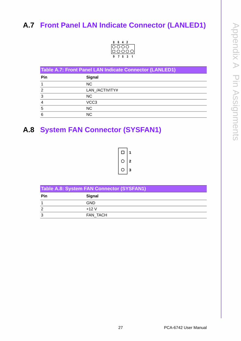
2.14 Front Panel LAN Indicate Connector (LANLED1)This LED is active for LAN connect
2.15 System FAN Connector (SYSFAN1)If fan is used, this connector supports cooling fans of 500 mA (6 W) or less.
2.16 AT Power Connector (PWR1)If you prefer not to acquire power through the PCA-6742 backplane via the gold H-connectors, the big 4P power connector (PWR1) also provides power input connec-tors for +5 V, and +12 V.
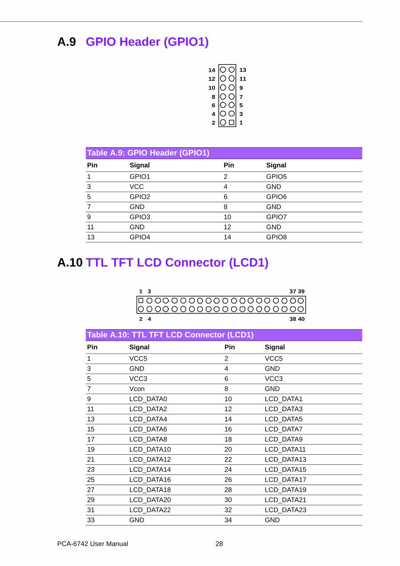
2.17 GPIO Header (GPIO1)Provides 14-pin header for digital I/O usage. Refer to Appendix B for detailed infor-mation on the pin assignments and programming guide in Appendix C.
The board supports 8-bit GPIO through GPIO connector. The 8 digital in- and out-puts can be programmed to read or control devices, with input or output defined. ThisGPIO is CMOS level (0 ~ 3.3 V).
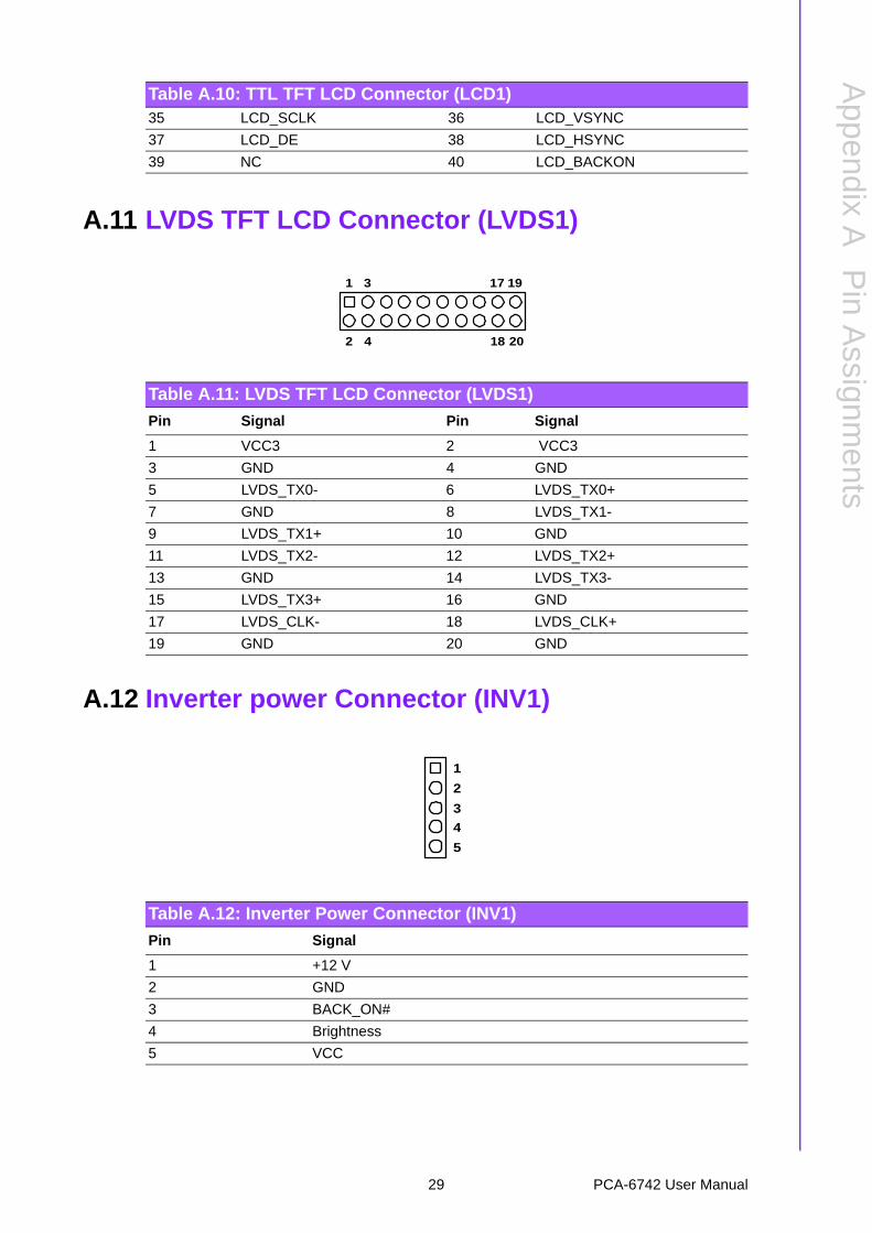
2.18 Flat Panel Display Connector (LCD1 & LVDS1)PCA-6742 is capable of driving flat panel displays.
2.18.1 TTL TFT LCD Connector (LCD1)For PCM-6742, LCD1 consists of a 40-pin connector which can support 1024x768 @18/24-bit TTL TFT LCD panel.
2.18.2 LVDS TFT LCD Connector (LVDS1) (Optional)For PCM-6742, LVDS1 consists of a 20-pin connector which can support 1024x768@ 18/24-bit LVDS TFT LCD panel (optional).
2.19 PC/104 Connector (PC104)The PCA-6742 is equipped with a 8/16 bit ISA signal PC/104 connector for futureexpansion.
PCA-6742 User Manual 10
Chapter 3
3 BIOS Operation This chapter describes how to set BIOS configuration data.
3.1 BIOS IntroductionAdvantech provides the fully-featured AwardBIOS 6.0 which delivers superior perfor-mance, compatibility and functionality. It’s many options and extensions let you cus-tomize your products to a wide range of designs and target markets.
The modular, adaptable AwardBIOS 6.0 supports the broadest range of third-partyperipherals and all popular chipsets, plus Intel, AMD, nVidia, VIA, and compatibleCPUs from 386 through Pentium and AMD Geode, K7 and K8 (including multiple pro-cessor platforms), and VIA Eden C3 and C7 CPU. Use Advantech’s utilities to selectand install features your customers need.
3.2 BIOS SetupPCA-6742 AwardBIOS 6.0 with CMOS SETUP utility allows users to configurerequired settings or to activate certain system features.
The CMOS SETUP saves the configuration in the CMOS RAM of the motherboard.When the power is turned off, the battery on the board supplies the necessary powerto the CMOS RAM.
When the power is turned on, press the <Del> button during the BIOS POST (Power-On Self Test) will take you to the CMOS SETUP screen.
CONTROL KEYS
< ↑ >< ↓ >< ← >< → > Move to select item
<Enter> Select Item
<Esc> Main Menu - Quit and not save changes into CMOSSub Menu - Exit current page and return to Main Menu
<Page Up/+> Increase the numeric value or make changes
<Page Down/-> Decrease the numeric value or make changes
<F1> General help, for Setup Sub Menu
<F2> Item Help
<F5> Load Previous Values
<F7> Load Optimized Default
<F10> Save all CMOS changes
PCA-6742 User Manual 12

Chapter 3
BIO
S O
peration
3.2.1 Main MenuPress <Del> to enter AwardBIOS CMOS Setup Utility, the Main Menu will appear onthe screen. Use arrow keys to select among the items and press <Enter> to accept orenter the sub-menu.
Standard CMOS FeaturesThis setup page includes all the items in standard compatible BIOS.
Advanced BIOS FeaturesThis setup page includes all the items of Award BIOS enhanced features.
Advanced Chipset FeaturesThis setup page includes all the items of Chipset’s advanced configuration features.
Integrated PeripheralsThis setup page includes all onboard peripheral devices.
PnP/PCI ConfigurationsThis item allows the user to change the Plug and Play and PCI resource settingssuch as IRQ for VGA and USB.
PC Health StatusThis item allows the user to monitor the system such as CPU, system temperatureand voltage.
Load Optimized DefaultsThis setup page includes Load Optimized system values for best performance con-figuration.
Set PasswordEstablish, change or disable password.
Save & Exit SetupSave CMOS value settings to CMOS and exit BIOS setup.
Exit Without SavingAbandon all CMOS value changes and exit BIOS setup.
13 PCA-6742 User Manual
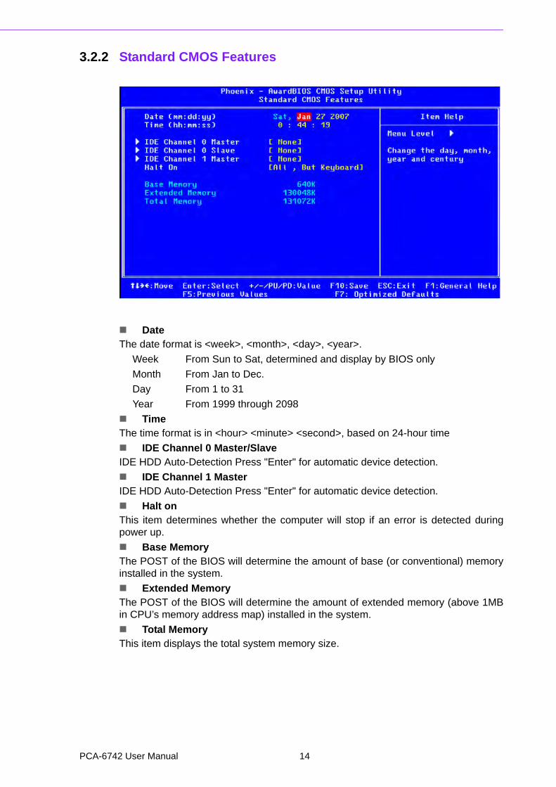
3.2.2 Standard CMOS Features
DateThe date format is <week>, <month>, <day>, <year>.
Week From Sun to Sat, determined and display by BIOS only
Month From Jan to Dec.
Day From 1 to 31
Year From 1999 through 2098
TimeThe time format is in <hour> <minute> <second>, based on 24-hour time
IDE Channel 0 Master/SlaveIDE HDD Auto-Detection Press "Enter" for automatic device detection.
IDE Channel 1 MasterIDE HDD Auto-Detection Press "Enter" for automatic device detection.
Halt onThis item determines whether the computer will stop if an error is detected duringpower up.
Base MemoryThe POST of the BIOS will determine the amount of base (or conventional) memoryinstalled in the system.
Extended MemoryThe POST of the BIOS will determine the amount of extended memory (above 1MBin CPU’s memory address map) installed in the system.
Total MemoryThis item displays the total system memory size.
PCA-6742 User Manual 14
Chapter 3
BIO
S O
peration
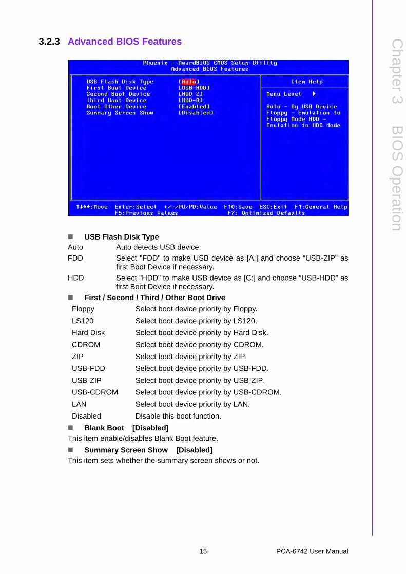
3.2.3 Advanced BIOS Features
USB Flash Disk TypeAuto Auto detects USB device.
FDD Select "FDD" to make USB device as [A:] and choose “USB-ZIP” asfirst Boot Device if necessary.
HDD Select "HDD" to make USB device as [C:] and choose “USB-HDD” asfirst Boot Device if necessary.
First / Second / Third / Other Boot Drive
Floppy Select boot device priority by Floppy.
LS120 Select boot device priority by LS120.
Hard Disk Select boot device priority by Hard Disk.
CDROM Select boot device priority by CDROM.
ZIP Select boot device priority by ZIP.
USB-FDD Select boot device priority by USB-FDD.
USB-ZIP Select boot device priority by USB-ZIP.
USB-CDROM Select boot device priority by USB-CDROM.
LAN Select boot device priority by LAN.
Disabled Disable this boot function.
Blank Boot [Disabled]This item enable/disables Blank Boot feature.
Summary Screen Show [Disabled]This item sets whether the summary screen shows or not.
15 PCA-6742 User Manual

3.2.4 Advanced Chipset Features
SMI712 VGA Setting [Press Enter] (Show Only)This item allows users to set VGA related features.
EVA-X4300 IDE Legacy mode [Enabled]This item enables EVA-X4300 IDE as legacy IDE controller or PCI IDE controller.
Watch Dog Timer reset [Disabled]This item allows users to set watchdog timer.
Do CMOS Clear [Disabled]This item allows users to clear CMOS.
LAN Controller [Enabled]This item enable or disables the onboard LAN controller.
GPCS0 FUNCTION [Disable]This item allows users to use GPCS function to detect ISA card.
GPCS COMMAND [MEMRW 16 Bits]Select 8-Bit, 16-Bit I/O or Memory card.
GPCS Start Address [Press Enter]Setting ISA card decode start address.
GPCS Mask Compare Bit [Press Enter]Setting ISA card range.
Ex: FFFFFFF0h mean range is 16 bytes, if FFFFFF00h mean range is 256 bytes.
Note! This “Advanced Chipset Features” option controls the configuration of the board’s chipset, this section is designed to be chipset independent, for controlling chipset register settings and fine tuning system perfor-mance. It is strongly recommended only technical users make changes to the default settings.
PCA-6742 User Manual 16
Chapter 3
BIO
S O
peration
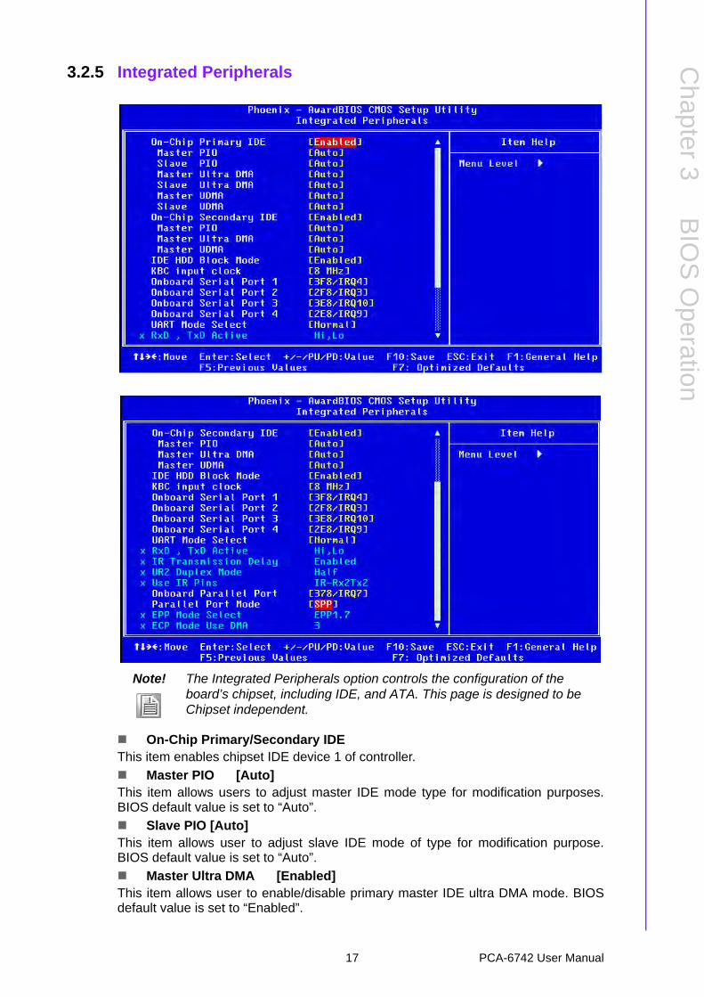
3.2.5 Integrated Peripherals
On-Chip Primary/Secondary IDE This item enables chipset IDE device 1 of controller.
Master PIO [Auto] This item allows users to adjust master IDE mode type for modification purposes.BIOS default value is set to “Auto”.
Slave PIO [Auto] This item allows user to adjust slave IDE mode of type for modification purpose.BIOS default value is set to “Auto”.
Master Ultra DMA [Enabled] This item allows user to enable/disable primary master IDE ultra DMA mode. BIOSdefault value is set to “Enabled”.
Note! The Integrated Peripherals option controls the configuration of the board’s chipset, including IDE, and ATA. This page is designed to be Chipset independent.
17 PCA-6742 User Manual
Slave Ultra DMA [Enabled] This item allows user to enable/disable primary slave IDE ultra DMA mode. BIOSdefault value is set to “Enabled”.
Master UDMA [Auto] This item allows user to adjust primary master IDE mode of type for modification pur-pose. BIOS default value is set to “Auto”.
Slave UDMA [Auto] This item allows user to adjust primary slave IDE mode of type for modification pur-pose. BIOS default value is set to “Auto”.
IDE HDD Block Mode [Enabled] This item allows enabled or disabled that IDE block data transfer mode. It will speedup HDD data transfer of efficiency. BIOS default value is set to “Enabled”.
CKB input clock [8 MHz] PS/2 keyboard communicates with the keyboard controller. The speed of the datalink depends on the clock signal generated by the keyboard controller.
Onboard Serial Port 1 [3F8 / IRQ4] This item allows user to change COM 1 address and IRQ.
Onboard Serial Port 2 [2F8 / IRQ3] This item allows user to change COM 2 address and IRQ.
Onboard Serial Port 3 [3E8 / IRQ10]This item allows user to change COM 3 address and IRQ.
Onboard Serial Port 4 [2E8 / IRQ9] This item allows user to change COM 4 address and IRQ.
UART Mode select [Normal] This item allows you to select UART mode.
RxD, TxD Active [Hi, Lo] This item allows you to determine the activity of RxD, TxD.
IR Transmission Delay [Enabled] This item allows you to enable or disable IR transmission delay.
UR2 Duplex Mode [Half] This item allows you to select the IR half/full duplex function.
Onboard Parallel Port [378 / IRQ7] This field sets the address of the on-board parallel port connector. You can selecteither Auto, 3BCH/IRQ7, 378H/IRQ7, 278H/IRQ5 or Disabled. If you install an I/Ocard with a parallel port, make sure there is no conflict in the address assignments.The CPU card can support up to three parallel ports, as long as there are no conflictsfor each port.
Parallel Port Mode [SPP] This field allows you to set the operation mode of the parallel port. The setting SPPallows normal speed operation, but in one direction only. EPP allows bidirectionalparallel port operation at maximum speed. ECP allows the parallel port to operate inbi-directional mode and at a speed faster than the maximum data transfer rate. “ECP+ EPP” allows normal speed operation in a two-way mode
EPP Mode Select [EPP1.7] This field allows you to select EPP port type 1.7 or 1.9.
ECP Mode Use DMA [3] This selection is available only if you select “ECP” or “ECP + EPP” in the Parallel PortMode field. In ECP Mode Use DMA, you can select DMA channel 1, DMA channel 3,or Disable. Leave this field on the default setting.
PCA-6742 User Manual 18

Chapter 3
BIO
S O
peration
3.2.6 PnP/PCI Configurations
Resources Controlled by [Auto(ESCD)] The commands here are “Auto” or “Manual”. Choosing “manual” requires you tochoose resources from each following sub-menu. Auto automatically configures theentire boot and Plug and Play devices but you must be using Windows 95 or above.
3.2.7 Load Optimized Defaults
Note! Load Optimized Defaults loads the default system values directly from ROM. If the stored record created by the Setup program should ever become corrupted (and therefore unusable). These defaults will load automatically when you turn PCA-6742 on.
19 PCA-6742 User Manual
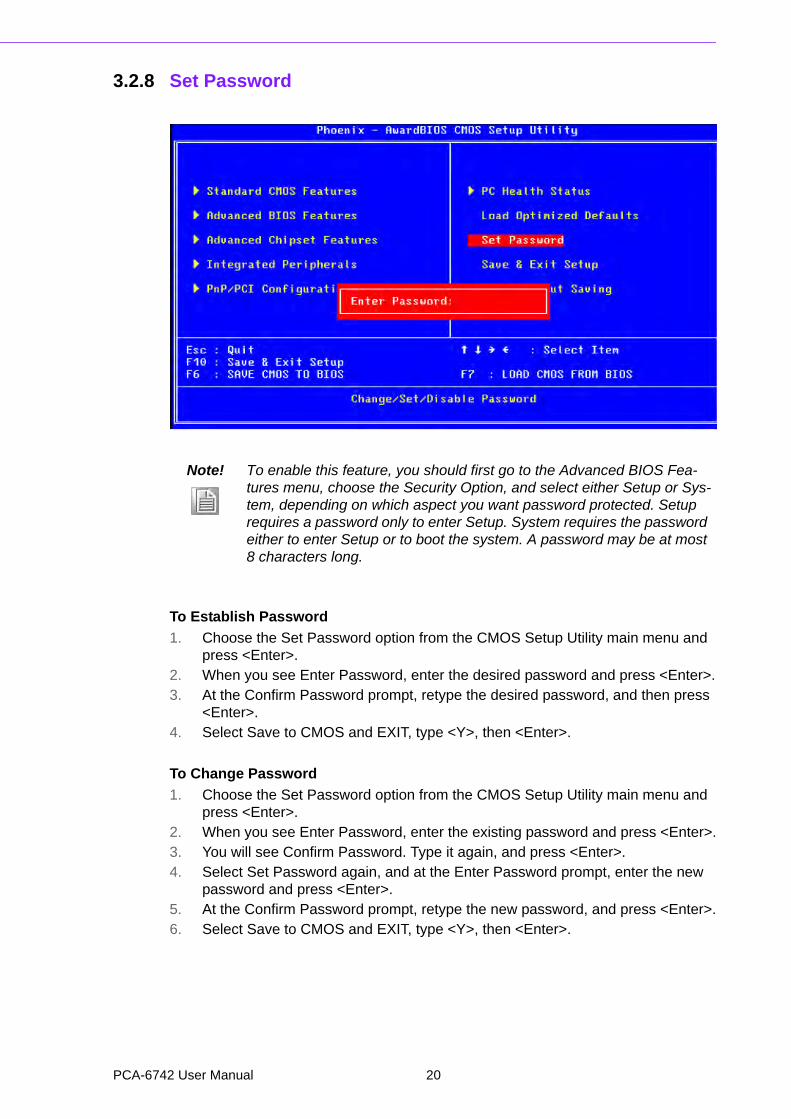
3.2.8 Set Password
To Establish Password
1. Choose the Set Password option from the CMOS Setup Utility main menu and press <Enter>.
2. When you see Enter Password, enter the desired password and press <Enter>.3. At the Confirm Password prompt, retype the desired password, and then press
<Enter>.4. Select Save to CMOS and EXIT, type <Y>, then <Enter>.
To Change Password
1. Choose the Set Password option from the CMOS Setup Utility main menu and press <Enter>.
2. When you see Enter Password, enter the existing password and press <Enter>.3. You will see Confirm Password. Type it again, and press <Enter>.4. Select Set Password again, and at the Enter Password prompt, enter the new
password and press <Enter>.5. At the Confirm Password prompt, retype the new password, and press <Enter>.6. Select Save to CMOS and EXIT, type <Y>, then <Enter>.
Note! To enable this feature, you should first go to the Advanced BIOS Fea-tures menu, choose the Security Option, and select either Setup or Sys-tem, depending on which aspect you want password protected. Setup requires a password only to enter Setup. System requires the password either to enter Setup or to boot the system. A password may be at most 8 characters long.
PCA-6742 User Manual 20
Chapter 3
BIO
S O
peration
To Disable Password
1. Choose the Set Password option from the CMOS Setup Utility main menu and press <Enter>.
2. When you see Enter Password, enter the existing password and press <Enter>.3. You will see Confirm Password. Type it again, and press <Enter>.4. Select Set Password again, and at the Enter Password prompt, please don’t
enter anything; just press <Enter>.5. At the Confirm Password prompt, again, don’t type in anything; just press
<Enter>.6. Select Save to CMOS and EXIT, type <Y>, then <Enter>.
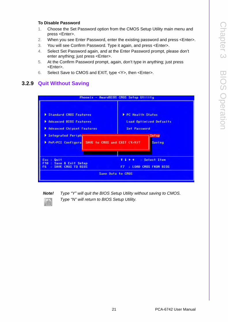
3.2.9 Quit Without Saving
Note! Type “Y” will quit the BIOS Setup Utility without saving to CMOS.
Type “N” will return to BIOS Setup Utility.
21 PCA-6742 User Manual

PCA-6742 User Manual 22

Appendix A
A Pin Assignments This appendix contains informa-tion of a detailed or specialized nature.
A.1 Front Panel Connectors (JFP1)
A.2 Front Panel Connectors (JFP2)
Table A.1: Front Panel Connectors (JFP1)
Pin Signal
1 HDD LED+
2 HDD LED-
3 Power LED+
4 Power LED-
5 N/C
6 N/C
7 Reset Switch
8 GND
9 5 VSB (Reserved)
10 Power Switch (Reserved)
3
64
5
2 8
97
10
1
Table A.2: Front Panel Connectors (JFP2)
Pin Signal
1 5 V
2 Fail LED
3 Buzzer_P1
4 Buzzer_P2
1 2 43
PCA-6742 User Manual 24
Appendix A
Pin A
ssignments
A.3 USB Ports (USB12 & USB34)
A.4 Serial Ports (COM2)
Table A.3: USB Ports (USB12 & USB34)
Pin Signal
1 VCC
2 VCC
3 USB Data1-
4 USB Data2-
5 USB Data1+
6 USB Data2+
7 GND
8 GND
9 GND
3
64
5
2 8
971
Table A.4: Serial Ports (COM2)
Pin Signal
RS-232 RS-422 RS-485
1 DCD TXD- Data-
2 DSR NC NC
3 RX TXD+ Data+
4 RTS NC NC
5 TX RXD+ NC
6 CTS NC NC
7 DTR RXD- NC
8 RI NC NC
9 GND GND GND
3
64
5
2 8
971
25 PCA-6742 User Manual
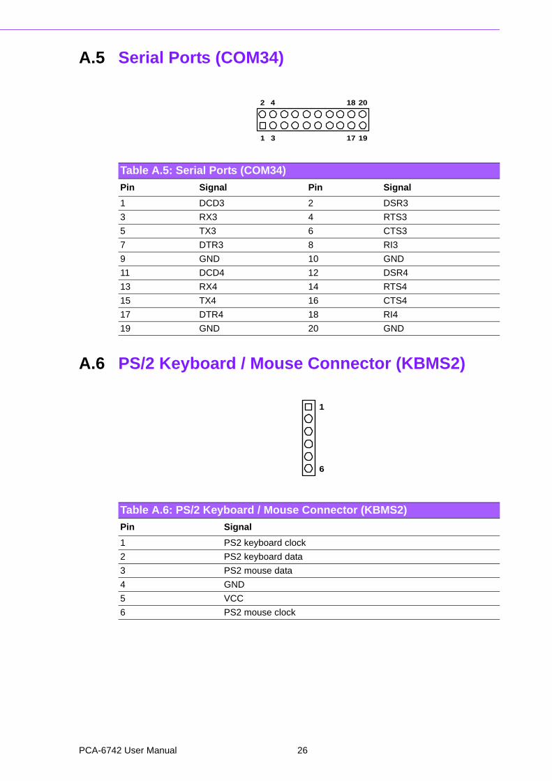
A.5 Serial Ports (COM34)
A.6 PS/2 Keyboard / Mouse Connector (KBMS2)
Table A.5: Serial Ports (COM34)
Pin Signal Pin Signal
1 DCD3 2 DSR3
3 RX3 4 RTS3
5 TX3 6 CTS3
7 DTR3 8 RI3
9 GND 10 GND
11 DCD4 12 DSR4
13 RX4 14 RTS4
15 TX4 16 CTS4
17 DTR4 18 RI4
19 GND 20 GND
171
2 18
3
4 20
19
Table A.6: PS/2 Keyboard / Mouse Connector (KBMS2)
Pin Signal
1 PS2 keyboard clock
2 PS2 keyboard data
3 PS2 mouse data
4 GND
5 VCC
6 PS2 mouse clock
6
1
PCA-6742 User Manual 26
Appendix A
Pin A
ssignments
A.7 Front Panel LAN Indicate Connector (LANLED1)
A.8 System FAN Connector (SYSFAN1)
Table A.7: Front Panel LAN Indicate Connector (LANLED1)
Pin Signal
1 NC
2 LAN_/ACTIVITY#
3 NC
4 VCC3
5 NC
6 NC
3
6 4
5
28
9 7 1
Table A.8: System FAN Connector (SYSFAN1)
Pin Signal
1 GND
2 +12 V
3 FAN_TACH
1
2
3
27 PCA-6742 User Manual
A.9 GPIO Header (GPIO1)
A.10 TTL TFT LCD Connector (LCD1)
Table A.9: GPIO Header (GPIO1)
Pin Signal Pin Signal
1 GPIO1 2 GPIO5
3 VCC 4 GND
5 GPIO2 6 GPIO6
7 GND 8 GND
9 GPIO3 10 GPIO7
11 GND 12 GND
13 GPIO4 14 GPIO8
3
1
14
10
8
6
4
2
12
5
7
9
11
13
Table A.10: TTL TFT LCD Connector (LCD1)
Pin Signal Pin Signal
1 VCC5 2 VCC5
3 GND 4 GND
5 VCC3 6 VCC3
7 Vcon 8 GND
9 LCD_DATA0 10 LCD_DATA1
11 LCD_DATA2 12 LCD_DATA3
13 LCD_DATA4 14 LCD_DATA5
15 LCD_DATA6 16 LCD_DATA7
17 LCD_DATA8 18 LCD_DATA9
19 LCD_DATA10 20 LCD_DATA11
21 LCD_DATA12 22 LCD_DATA13
23 LCD_DATA14 24 LCD_DATA15
25 LCD_DATA16 26 LCD_DATA17
27 LCD_DATA18 28 LCD_DATA19
29 LCD_DATA20 30 LCD_DATA21
31 LCD_DATA22 32 LCD_DATA23
33 GND 34 GND
402
1 39
4
3 37
38
PCA-6742 User Manual 28
Appendix A
Pin A
ssignments
A.11 LVDS TFT LCD Connector (LVDS1)
A.12 Inverter power Connector (INV1)
35 LCD_SCLK 36 LCD_VSYNC
37 LCD_DE 38 LCD_HSYNC
39 NC 40 LCD_BACKON
Table A.10: TTL TFT LCD Connector (LCD1)
Table A.11: LVDS TFT LCD Connector (LVDS1)
Pin Signal Pin Signal
1 VCC3 2 VCC3
3 GND 4 GND
5 LVDS_TX0- 6 LVDS_TX0+
7 GND 8 LVDS_TX1-
9 LVDS_TX1+ 10 GND
11 LVDS_TX2- 12 LVDS_TX2+
13 GND 14 LVDS_TX3-
15 LVDS_TX3+ 16 GND
17 LVDS_CLK- 18 LVDS_CLK+
19 GND 20 GND
182
1 17
4
3 19
20
Table A.12: Inverter Power Connector (INV1)
Pin Signal
1 +12 V
2 GND
3 BACK_ON#
4 Brightness
5 VCC
1
5
2
3
4
29 PCA-6742 User Manual

PCA-6742 User Manual 30

Appendix B
B Programming the Watchdog Timer This appendix contains informa-tion of how to program the Watch-dog Timer.
B.1 IntroductionThe PCA-6742’s watchdog timer can be used to monitor system software operationand take corrective action if the software fails to function within the programmedperiod. This section describes the operation of the watchdog timer and how to pro-gram it.
B.1.1 Watchdog Timer OverviewThe watchdog timer is built in to the W83627HG super I/O controller. It provides thefollowing user programmable functions:
Can be enabled and disabled by user programming Timer can be set from 1 to 255 seconds or 1 to 255 minutes Generates an interrupt or reset signal if the software fails to reset the timer
before time-out
B.1.2 Programming the Watchdog Timer
The I/O port address of the watchdog timer is 2E (hex) and 2F (hex). 2E (hex) is theaddress port. 2F (hex) is the data port. You must first write an address value intoaddress port 2E (hex), then write/read data to/from the assigned register throughdata port 2F (hex).
PCA-6742 User Manual 32
Appendix B
Program
ming
theW
atchdogT
imer
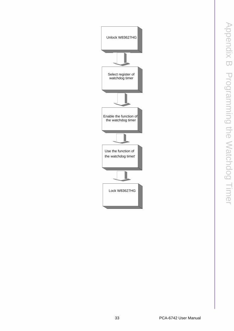
Unlock W83627HG
Select register of watchdog timer
Enable the function ofthe watchdog timer
Use the function of
the watchdog timer
Lock W83627HG
33 PCA-6742 User Manual
B.1.2 Example Program1. Enable watchdog timer and set 10 sec. as timeout interval
;-----------------------------------------------------------
Mov dx,2eh ; Unlock W83627HG
Mov al,87h
Out dx,al
Out dx,al
;-----------------------------------------------------------
Mov al,07h ; Select registers of watchdog timer
Out dx,al
Inc dx
Mov al,08h
Out dx,al
;-----------------------------------------------------------
Dec dx ; Enable the function of watchdog timer
Mov al,30h
Out dx,al
Inc dx
Mov al,01h
Out dx,al
;-----------------------------------------------------------
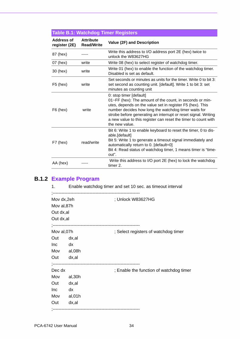
Table B.1: Watchdog Timer Registers
Address of register (2E)
Attribute Read/Write
Value (2F) and Description
87 (hex) ----- Write this address to I/O address port 2E (hex) twice to unlock the W83627HG
07 (hex) write Write 08 (hex) to select register of watchdog timer.
30 (hex) write Write 01 (hex) to enable the function of the watchdog timer. Disabled is set as default.
F5 (hex) write Set seconds or minutes as units for the timer. Write 0 to bit 3: set second as counting unit. [default]. Write 1 to bit 3: set minutes as counting unit
F6 (hex) write
0: stop timer [default] 01~FF (hex): The amount of the count, in seconds or min-utes, depends on the value set in register F5 (hex). This number decides how long the watchdog timer waits for strobe before generating an interrupt or reset signal. Writing a new value to this register can reset the timer to count with the new value.
F7 (hex) read/write
Bit 6: Write 1 to enable keyboard to reset the timer, 0 to dis-able.[default] Bit 5: Write 1 to generate a timeout signal immediately and automatically return to 0. [default=0] Bit 4: Read status of watchdog timer, 1 means timer is “time-out”.
AA (hex) ----- Write this address to I/O port 2E (hex) to lock the watchdog timer 2.
PCA-6742 User Manual 34
Appendix B
Program
ming
theW
atchdogT
imer
Dec dx ; Set second as counting unit
Mov al,0f5h
Out dx,al
Inc dx
In al,dx
And al,not 08h
Out dx,al
;-----------------------------------------------------------
Dec dx ; Set timeout interval as 10 seconds and start counting
Mov al,0f6h
Out dx,al
Inc dx
Mov al,10
Out dx,al
;-----------------------------------------------------------
Dec dx ; lock W83627HG
Mov al,0aah
Out dx,al
2. Enable watchdog timer and set 5 minutes as timeout interval
;-----------------------------------------------------------
Mov dx,2eh ; unlock W83627HG
Mov al,87h
Out dx,al
Out dx,al
;-----------------------------------------------------------
Mov al,07h ; Select registers of watchdog timer
Out dx,al
Inc dx
Mov al,08h
Out dx,al
;-----------------------------------------------------------
Dec dx ; Enable the function of watchdog timer
Mov al,30h
Out dx,al
Inc dx
Mov al,01h
Out dx,al
;-----------------------------------------------------------
Dec dx ; Set minute as counting unit
Mov al,0f5h
Out dx,al
Inc dx
In al,dx
Or al,08h
Out dx,al
35 PCA-6742 User Manual
;-----------------------------------------------------------
Dec dx ; Set timeout interval as 5 minutes and start counting
Mov al,0f6h
Out dx,al
Inc dx
Mov al,5
Out dx,al
;-----------------------------------------------------------
Dec dx ; lock W83627HG
Mov al,0aah
Out dx,al
3. Enable watchdog timer to be reset by mouse
;-----------------------------------------------------------
Mov dx,2eh ; unlock W83627HG
Mov al,87h
Out dx,al
Out dx,al
;-----------------------------------------------------------
Mov al,07h ; Select registers of watchdog timer
Out dx,al
Inc dx
Mov al,08h
Out dx,al
;-----------------------------------------------------------
Dec dx ; Enable the function of watchdog timer
Mov al,30h
Out dx,al
Inc dx
Mov al,01h
Out dx,al
;-----------------------------------------------------------
Dec dx ; Enable watchdog timer to be reset by mouse
Mov al,0f7h
Out dx,al
Inc dx
In al,dx
Or al,80h
Out dx,al
;-----------------------------------------------------------
Dec dx ; lock W83627HG
Mov al,0aah
Out dx,al
4. Enable watchdog timer to be reset by keyboard
;-----------------------------------------------------------
Mov dx,2eh ; unlock W83627HG
PCA-6742 User Manual 36
Appendix B
Program
ming
theW
atchdogT
imer
Mov al,87h
Out dx,al
Out dx,al
;-----------------------------------------------------------
Mov al,07h ; Select registers of watchdog timer
Out dx,al
Inc dx
Mov al,08h
Out dx,al
;-----------------------------------------------------------
Dec dx ; Enable the function of watchdog timer
Mov al,30h
Out dx,al
Inc dx
Mov al,01h
Out dx,al
;-----------------------------------------------------------
Dec dx ; Enable watchdog timer to be strobed reset by keyboard
Mov al,0f7h
Out dx,al
Inc dx
In al,dx
Or al,40h
Out dx,al
;-----------------------------------------------------------
Dec dx ; lock W83627HG
Mov al,0aah
Out dx,al
5. Generate a time-out signal without timer counting
;-----------------------------------------------------------
Mov dx,2eh ; unlock W83627HG
Mov al,87h
Out dx,al
Out dx,al
;-----------------------------------------------------------
Mov al,07h ; Select registers of watchdog timer
Out dx,al
Inc dx
Mov al,08h
Out dx,al
;-----------------------------------------------------------
Dec dx ; Enable the function of watchdog timer
Mov al,30h
Out dx,al
Inc dx
37 PCA-6742 User Manual

Mov al,01h
Out dx,al
;-----------------------------------------------------------
Dec dx ; Generate a time-out signal
Mov al,0f7h
Out dx,al ;Write 1 to bit 5 of F7 register
Inc dx
In al,dx
Or al,20h
Out dx,al
;-----------------------------------------------------------
Dec dx ; lock W83627HG
Mov al,0aah
Out dx,al
PCA-6742 User Manual 38
Appendix C
C System Assignments This appendix contains informa-tion of all System assignments.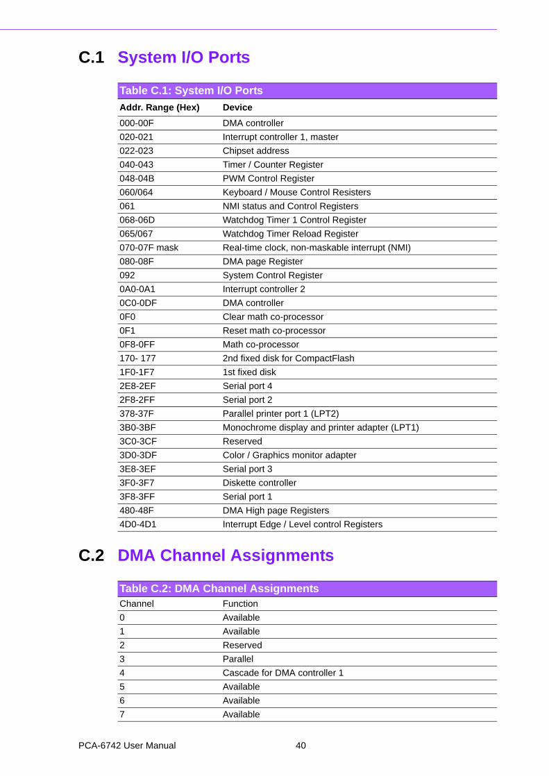
C.1 System I/O Ports
C.2 DMA Channel Assignments
Table C.1: System I/O Ports
Addr. Range (Hex) Device
000-00F DMA controller
020-021 Interrupt controller 1, master
022-023 Chipset address
040-043 Timer / Counter Register
048-04B PWM Control Register
060/064 Keyboard / Mouse Control Resisters
061 NMI status and Control Registers
068-06D Watchdog Timer 1 Control Register
065/067 Watchdog Timer Reload Register
070-07F mask Real-time clock, non-maskable interrupt (NMI)
080-08F DMA page Register
092 System Control Register
0A0-0A1 Interrupt controller 2
0C0-0DF DMA controller
0F0 Clear math co-processor
0F1 Reset math co-processor
0F8-0FF Math co-processor
170- 177 2nd fixed disk for CompactFlash
1F0-1F7 1st fixed disk
2E8-2EF Serial port 4
2F8-2FF Serial port 2
378-37F Parallel printer port 1 (LPT2)
3B0-3BF Monochrome display and printer adapter (LPT1)
3C0-3CF Reserved
3D0-3DF Color / Graphics monitor adapter
3E8-3EF Serial port 3
3F0-3F7 Diskette controller
3F8-3FF Serial port 1
480-48F DMA High page Registers
4D0-4D1 Interrupt Edge / Level control Registers
Table C.2: DMA Channel AssignmentsChannel Function
0 Available
1 Available
2 Reserved
3 Parallel
4 Cascade for DMA controller 1
5 Available
6 Available
7 Available
PCA-6742 User Manual 40

Appendix C
System
Assignm
ents
C.3 Interrupt Assignments
C.4 1st MB Memory Map
Table C.3: Interrupt Assignments
Interrupt# Interrupt Source
NMI Parity error detected
IRQ 0 Interval timer
IRQ 1 Keyboard
IRQ 2 Interrupt from controller 2 (cascade)
IRQ 8 Real-time clock
IRQ 9 Serial communication port 4
IRQ 10 Available
IRQ 11 Available
IRQ 12 PS/2 mouse
IRQ 13 INT from co-processor
IRQ 14 Preliminary IDE
IRQ 15 Secondary IDE for CompactFlash
IRQ 3 Serial communication port 2
IRQ 4 Serial communication port 1
IRQ 5 Serial communication port 3
IRQ 6 Reserve
IRQ 7 Parallel port 1 (print port)
Table C.4: 1st MB Memory Map
Addr. range (Hex) Device
E000 - EFFF System ROM
C800 - DFFF Available
C000h - C7FFh VGA BIOS
B800h - BFFFh CGA/EGA/VGA text
B000h - B7FFh Reserved for graphic mode usage
A000h - AFFFh EGA/VGA graphics
0000h - 9FFFh Base memory
41 PCA-6742 User Manual

PCA-6742 User Manual 42

Appendix D
D Installing PC/104 ModulesThis appendix contains informa-tion of installing PC/104 modules.
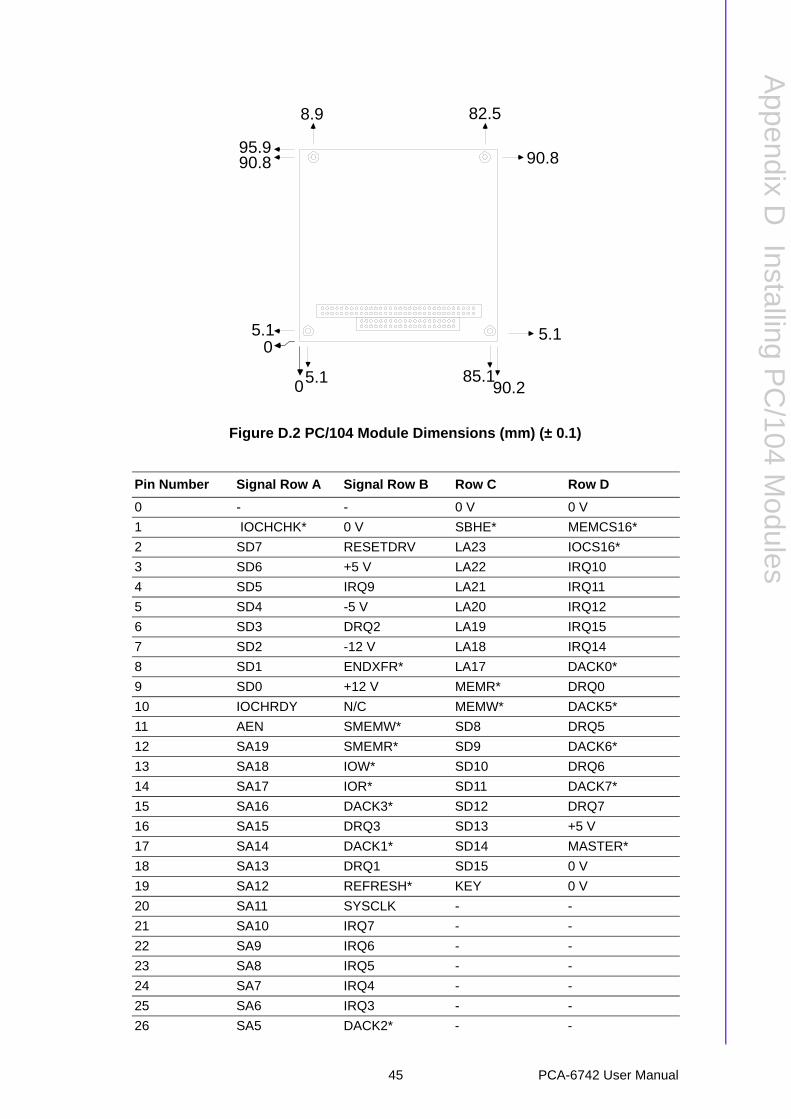
D.1 IntroductionThe PCA-6742 PC/104 connectors give you the flexibility to attach PC/104 modules.
Installing these modules on the PCA-6742 is quick and simple. The following stepsshow how to mount the PC/104 modules:
1. Remove the PCA-6742 from your system, paying particular attention to the safety instructions already mentioned above.
2. Make any jumper or link changes required to the CPU card now. Once the PC/104 module is mounted you may have difficulty in accessing these.
3. Normal PC/104 modules have male connectors and mount directly onto the main card (Refer to the diagram on the following page).
4. Mount the PC/104 module onto the CPU card by pressing the module firmly but carefully onto the mounting connectors.
5. Secure the PC/104 module onto the CPU card using the four mounting spacers and screws.
Figure D.1 PC/104 Module Mounting Diagram
PC/104Mounting Support
Female
PCA-6742
Male
PC/104 Module
PCA-6742 User Manual 44
Appendix D
InstallingP
C/104
Modules
Figure D.2 PC/104 Module Dimensions (mm) (± 0.1)
Pin Number Signal Row A Signal Row B Row C Row D
0 - - 0 V 0 V
1 IOCHCHK* 0 V SBHE* MEMCS16*
2 SD7 RESETDRV LA23 IOCS16*
3 SD6 +5 V LA22 IRQ10
4 SD5 IRQ9 LA21 IRQ11
5 SD4 -5 V LA20 IRQ12
6 SD3 DRQ2 LA19 IRQ15
7 SD2 -12 V LA18 IRQ14
8 SD1 ENDXFR* LA17 DACK0*
9 SD0 +12 V MEMR* DRQ0
10 IOCHRDY N/C MEMW* DACK5*
11 AEN SMEMW* SD8 DRQ5
12 SA19 SMEMR* SD9 DACK6*
13 SA18 IOW* SD10 DRQ6
14 SA17 IOR* SD11 DACK7*
15 SA16 DACK3* SD12 DRQ7
16 SA15 DRQ3 SD13 +5 V
17 SA14 DACK1* SD14 MASTER*
18 SA13 DRQ1 SD15 0 V
19 SA12 REFRESH* KEY 0 V
20 SA11 SYSCLK - -
21 SA10 IRQ7 - -
22 SA9 IRQ6 - -
23 SA8 IRQ5 - -
24 SA7 IRQ4 - -
25 SA6 IRQ3 - -
26 SA5 DACK2* - -
8.9 82.5
90.8
5.1
90.285.15.10
5.10
95.990.8
45 PCA-6742 User Manual

27 SA4 TC - -
28 SA3 BALE - -
29 SA2 +5 V - -
30 SA1 OSC - -
31 SA0 0 V - -
32 0 V 0 V - -
* active low
PCA-6742 User Manual 46

Appendix E
E Mechanical Drawings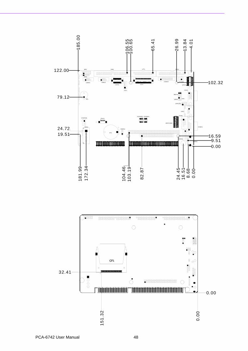
USB34 USB12
JFP1
JFP2
SP1
LVDS1
IDE1
INV1
LCD1
LPT1
JTAG1
BT1
CMOS1
SYSFAN1
PWR1
VGASW1VGASW2
JSETCOM2
COM34 JCASE1
FDD1
GPIO1
VGA1
JWDT1
JOBS1 JIR1
LANLED1
LAN1
COM2
COMD1
KBMS1
KBMS2
0.00
181.
99
16.5
1
0.00
185.
00
8.68
24.4
5
82.8
7
103.
1910
4.46
172.
34
19.5124.72
79.12
100.
6510
6.55
65.4
1
13.8
44.
01
26.9
9
122.00
102.32
16.599.51
CF1
151.
32
0.00
0.00
32.41
PCA-6742 User Manual 48

Appendix E
MechanicalD
rawings
49 PCA-6742 User Manual

www.advantech.comPlease verify specifications before quoting. This guide is intended for referencepurposes only.All product specifications are subject to change without notice.No part of this publication may be reproduced in any form or by any means,electronic, photocopying, recording or otherwise, without prior written permis-sion of the publisher.All brand and product names are trademarks or registered trademarks of theirrespective companies.© Advantech Co., Ltd. 2013
Related Documents


