User Guide | EVAL-ADN4680E UG-2010 Evaluating the ADN4680E 250 Mbps, Half-Duplex, Quad M-LVDS Transceivers PLEASE SEE THE LAST PAGE FOR AN IMPORTANT WARNING AND LEGAL TERMS AND CONDITIONS. Rev. 0 | 1 of 12 FEATURES ► Easy evaluation of the ADN4680E 250 Mbps, half-duplex, quad M-LVDS transceivers ► Board layout optimized for high speed signaling ► Matched track lengths on M-LVDS differential pairs with control- led 100 Ω differential impedance ► Matched track lengths on high speed DIx and ROx logic signals with controlled 50 Ω impedance to GND ► SMA jacks for connecting to high speed DIx and ROx logic signals and M-LVDS Ax and Bx signals ► Optional screw terminal connectors for accessing the ROx, REx, DEx, and DIx logic signals ► Power and ground connections through screw terminal blocks ► Jumper-selectable global power down via the ENP pin ► Jumper-selectable driver enable, receiver enable, and fail-safe for each transceiver via the REx, DEx, and FSx pins ► Test points for measuring all signals and multiple ground points to facilitate probing of multiple signals ► 100 Ω termination resistors across Ax and Bx signals to simulate a terminated bus EQUIPMENT NEEDED ► A 4 channel oscilloscope ► A signal generator ► A 3.0 V to 3.6 V power supply EVALUATION KIT CONTENTS ► EVAL-ADN4680EEBZ GENERAL DESCRIPTION The EVAL-ADN4680EEBZ allows quick and easy evaluation of the ADN4680E 250 Mbps, half-duplex, quad multipoint, low voltage differential signaling (M-LVDS) transceivers. The EVAL- ADN4680EEBZ allows the input and output functions of each trans- ceiver to be exercised without the need for external components. Subminiature A (SMA) connectors provide convenient connections for high speed logic and the M-LVDS bus signals. Screw terminal blocks are available to access power, ground, and digital signals. Jumper options allow control of each transceivers driver and receiv- er enable pins, each transceivers fail-safe functionality, and the global power-down mode. The EVAL-ADN4680EEBZ is optimized for high speed signaling. The differential M-LVDS signal traces on the board are routed as a length matched 100 Ω differential pair. The DIx digital input and ROx receiver output are also length matched and routed with a controlled 50 Ω impedance to ground. The EVAL-ADN4680EEBZ features a solid ground and power plane for optimum power integrity. The EVAL-ADN4680EEBZ has a footprint for the ADN4680E trans- ceivers in a 7 mm × 7 mm, 48-lead LFCSP. For full details on the ADN4680E, see the ADN4680E data sheet, which must be used in conjunction with this user guide when using the EVAL-ADN4680EEBZ.

Welcome message from author
This document is posted to help you gain knowledge. Please leave a comment to let me know what you think about it! Share it to your friends and learn new things together.
Transcript

User Guide | EVAL-ADN4680EUG-2010
Evaluating the ADN4680E 250 Mbps, Half-Duplex, Quad M-LVDS Transceivers
PLEASE SEE THE LAST PAGE FOR AN IMPORTANTWARNING AND LEGAL TERMS AND CONDITIONS.
Rev. 0 | 1 of 12
FEATURES
Easy evaluation of the ADN4680E 250 Mbps, half-duplex, quadM-LVDS transceivers
Board layout optimized for high speed signaling Matched track lengths on M-LVDS differential pairs with control-
led 100 Ω differential impedance Matched track lengths on high speed DIx and ROx logic signals
with controlled 50 Ω impedance to GND SMA jacks for connecting to high speed DIx and ROx logic
signals and M-LVDS Ax and Bx signals Optional screw terminal connectors for accessing the ROx, REx,
DEx, and DIx logic signals Power and ground connections through screw terminal blocks Jumper-selectable global power down via the ENP pin Jumper-selectable driver enable, receiver enable, and fail-safe
for each transceiver via the REx, DEx, and FSx pins Test points for measuring all signals and multiple ground points
to facilitate probing of multiple signals 100 Ω termination resistors across Ax and Bx signals to simulate
a terminated bus
EQUIPMENT NEEDED
A 4 channel oscilloscope A signal generator A 3.0 V to 3.6 V power supply
EVALUATION KIT CONTENTS
EVAL-ADN4680EEBZ
GENERAL DESCRIPTION
The EVAL-ADN4680EEBZ allows quick and easy evaluation ofthe ADN4680E 250 Mbps, half-duplex, quad multipoint, lowvoltage differential signaling (M-LVDS) transceivers. The EVAL-ADN4680EEBZ allows the input and output functions of each trans-ceiver to be exercised without the need for external components.Subminiature A (SMA) connectors provide convenient connectionsfor high speed logic and the M-LVDS bus signals. Screw terminalblocks are available to access power, ground, and digital signals.Jumper options allow control of each transceivers driver and receiv-er enable pins, each transceivers fail-safe functionality, and theglobal power-down mode.The EVAL-ADN4680EEBZ is optimized for high speed signaling.The differential M-LVDS signal traces on the board are routed asa length matched 100 Ω differential pair. The DIx digital input andROx receiver output are also length matched and routed with acontrolled 50 Ω impedance to ground. The EVAL-ADN4680EEBZfeatures a solid ground and power plane for optimum powerintegrity.The EVAL-ADN4680EEBZ has a footprint for the ADN4680E trans-ceivers in a 7 mm × 7 mm, 48-lead LFCSP.For full details on the ADN4680E, see the ADN4680E data sheet,which must be used in conjunction with this user guide when usingthe EVAL-ADN4680EEBZ.
User Guide EVAL-ADN4680ETABLE OF CONTENTS
analog.com Rev. 0 | 2 of 12
Features................................................................ 1Equipment Needed................................................1Evaluation Kit Contents......................................... 1General Description...............................................1EVAL-ADN4680EEBZ Evaluation BoardPhotograph.......................................................... 3
Evaluation Board Configuration.............................4
Setting Up the Evaluation Board........................ 4Input and Output Connections............................5Jumper Connections.......................................... 6
Evaluation Board Schematic and Layout...............8Ordering Information............................................12
Bill of Materials.................................................12
REVISION HISTORY
9/2021 —Revision 0: Initial Version
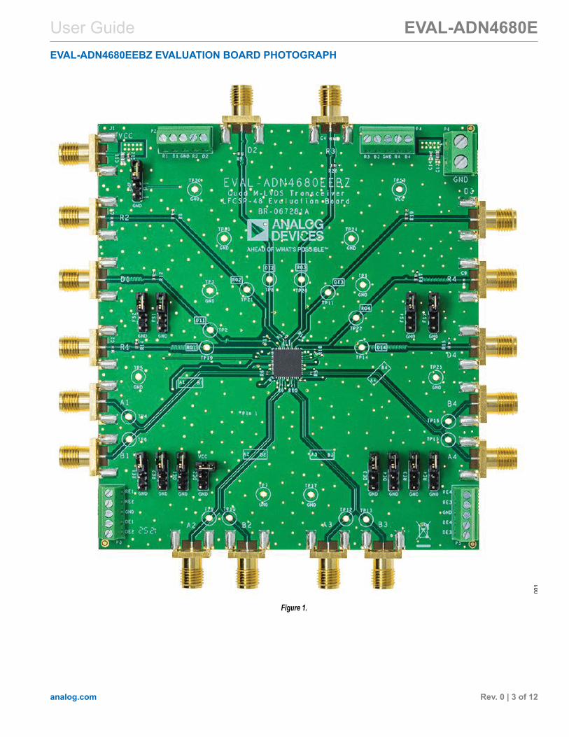
User Guide EVAL-ADN4680EEVAL-ADN4680EEBZ EVALUATION BOARD PHOTOGRAPH
analog.com Rev. 0 | 3 of 12
Figure 1.
User Guide EVAL-ADN4680EEVALUATION BOARD CONFIGURATION
analog.com Rev. 0 | 4 of 12
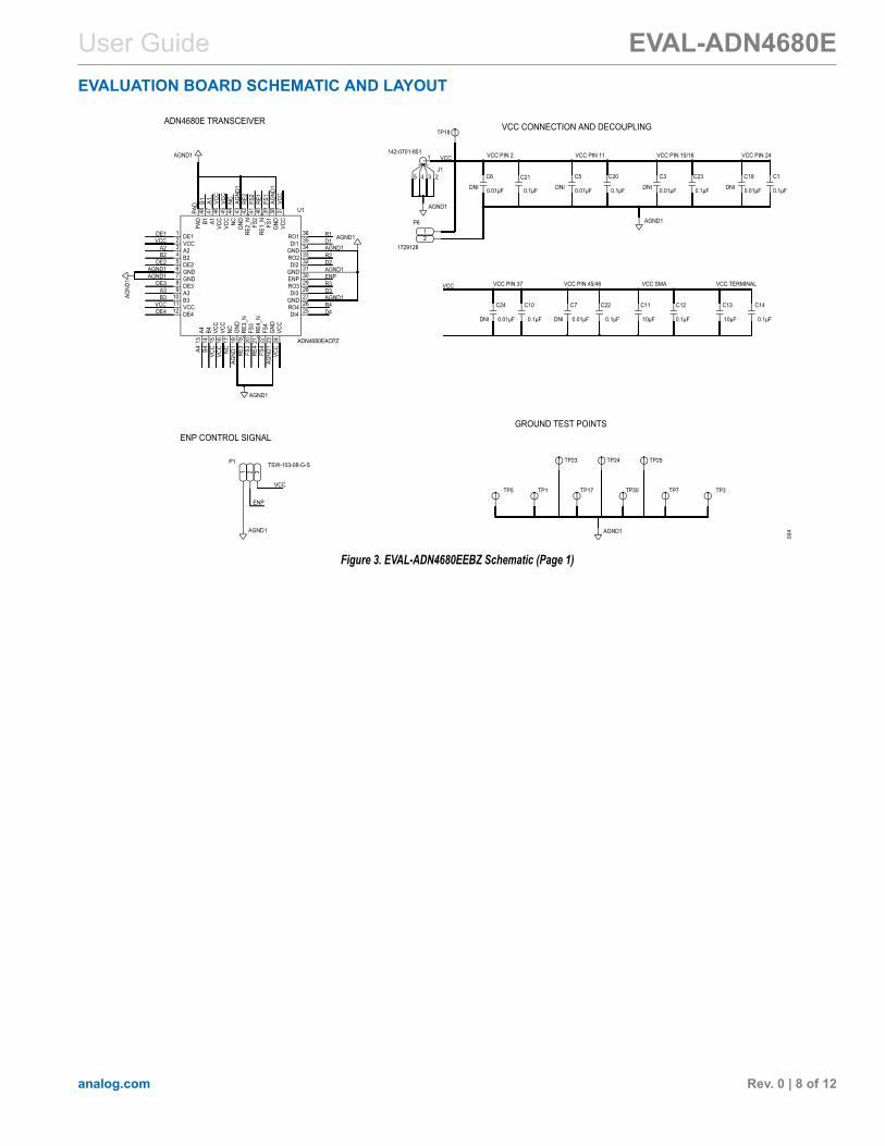
SETTING UP THE EVALUATION BOARDThe EVAL-ADN4680EEBZ allows the ADN4680E to be quicklyand easily evaluated. The EVAL-ADN4680EEBZ allows all of theinput and output functions to be exercised without the need forexternal components. Jumper configurations are shown in JumperConnections.The EVAL-ADN4680EEBZ is powered by connecting a 3.3 V powersupply to either the J1 VCC SMA connector or the VCC and GNDconnections of the P6 screw terminal block. The supply current istypically 8 mA with all drivers and receivers disabled. The C11 andC13, 10 μF decoupling capacitors and the C12 and C14, 100 nFdecoupling capacitors are fitted at the VCC connectors. Several100 nF decoupling capacitors are included at the supply pins of theADN4680E.Each half-duplex transceiver of the ADN4680E contains both adriver and receiver that can be individually enabled or disabled viajumper options. Each driver can be enabled or disabled via theDE1 to DE4 jumpers. Connect these jumpers to VCC to enablethe respective driver, and connect these jumpers to GND to disablethe respective driver. Similarly, each receiver can be enabled ordisabled via the RE1 to RE4 jumpers. Connect these jumpers toGND to enable the respective receiver, and connect these jumpersto VCC to disable the respective receiver. The DE1 to DE4 andRE1 to RE4 signals can also be accessed via the P3 and P5 screwterminal blocks for dynamic control via a processor or a signalgenerator.Each of the four receivers of the ADN4680E can be individuallyconfigured for Type 1 or Type 2 operation, using the FS1 to FS4jumpers. Connecting an FSx jumper to GND configures the respec-tive receiver for Type 1 operation, while removing the FSx jumper orconnecting the FSx jumper to VCC configures that receiver for Type2 operation.The ADN4680E features a global device enable pin, ENP, that canbe accessed via the P1 jumper. When this jumper is connectedto GND, all drivers and receivers are disabled in a low power
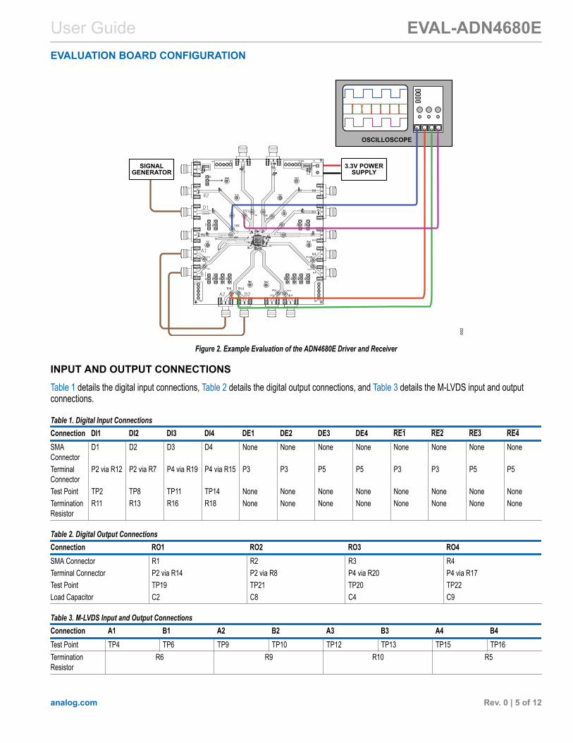
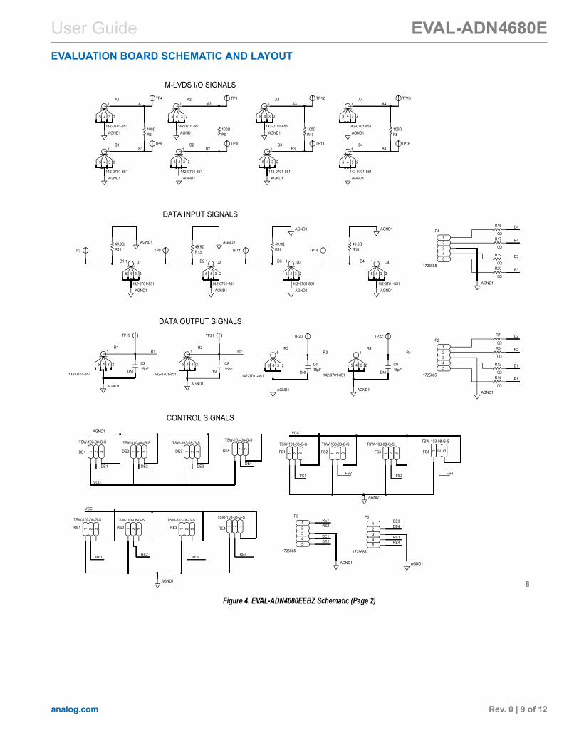
shutdown state. When this jumper is connected to VCC, the state ofeach transceiver is controlled via the DE1 to DE4 and RE1 to RE4pins.The ADN4680E high speed digital input signals, DI1 to DI4, andreceiver output signals, RO1 to RO4, are routed on length matchedtraces with a 50 Ω characteristic impedance to GND. The DI1to DI4 traces are terminated to GND with 50 Ω resistors, R11,R13, R16, and R18, respectively. The RO1 to RO4 traces includean optional placeholder for a load capacitor at C2, C8, C4, andC9, respectively. For optimum signal integrity, the DI1 to DI4 inputsignals and RO1 to RO4 output signals can be accessed viadedicated SMA connectors, D1 to D4 and R1 to R4. Alternativelythe P2 and P4 screw terminal connectors can be used for easy wireconnections to a microprocessor. The connections to the P2 andP4 screw terminal block are made via 0 Ω resistors, which can beremoved to eliminate any stub lengths along the interconnect.The M-LVDS input and output signals, A1 to A4 and B1 to B4, areaccessed via SMA connectors. These A1 and B1, A2 and B2, A3and B3, and A4 and B4 signals are routed as four length matcheddifferential pairs with a differential characteristic impedance of 100Ω. These signals are terminated at the Ax and Bx pins of theADN4680E with 100 Ω resistors, R6, R9, R10, and R5, respectively.An example evaluation of the ADN4680E driver and receiver isshown in Figure 2. A signal generator is connected via the D1 SMAconnector to DI1 with an input signal of 125 MHz, a 50% duty cycle,and a swing of between 0 V and 3.3 V. The ENP jumper, P1, isconnected to VCC to set the enable global device power-up. TheDE1 jumper is set to VCC, and the RE2 jumper is set to GND, toenable the driver of Transceiver 1 and the receiver of Transceiver 2,respectively. The DE2 jumper is set to GND to disable the driver ofTransceiver 2 to avoid bus contention. Jumper FS2 is set to GNDto set the receiver of Transceiver 2 to Type 1 operation. The A1SMA connector is connected to the A2 SMA connector, and theB1 SMA connector is connected to B2 SMA connector. In addition,oscilloscope probes are connected to DI1 (TP2), A2 (TP9), B2(TP10), and RO2 (TP21).
User Guide EVAL-ADN4680EEVALUATION BOARD CONFIGURATION
analog.com Rev. 0 | 5 of 12
Figure 2. Example Evaluation of the ADN4680E Driver and Receiver
INPUT AND OUTPUT CONNECTIONSTable 1 details the digital input connections, Table 2 details the digital output connections, and Table 3 details the M-LVDS input and outputconnections.
Table 1. Digital Input ConnectionsConnection DI1 DI2 DI3 DI4 DE1 DE2 DE3 DE4 RE1 RE2 RE3 RE4SMAConnector
D1 D2 D3 D4 None None None None None None None None
TerminalConnector
P2 via R12 P2 via R7 P4 via R19 P4 via R15 P3 P3 P5 P5 P3 P3 P5 P5
Test Point TP2 TP8 TP11 TP14 None None None None None None None NoneTerminationResistor
R11 R13 R16 R18 None None None None None None None None
Table 2. Digital Output ConnectionsConnection RO1 RO2 RO3 RO4SMA Connector R1 R2 R3 R4Terminal Connector P2 via R14 P2 via R8 P4 via R20 P4 via R17Test Point TP19 TP21 TP20 TP22Load Capacitor C2 C8 C4 C9
Table 3. M-LVDS Input and Output ConnectionsConnection A1 B1 A2 B2 A3 B3 A4 B4Test Point TP4 TP6 TP9 TP10 TP12 TP13 TP15 TP16TerminationResistor
R6 R9 R10 R5
User Guide EVAL-ADN4680EEVALUATION BOARD CONFIGURATION
analog.com Rev. 0 | 6 of 12
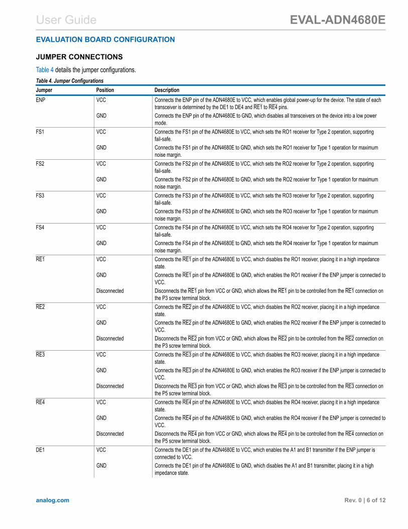
JUMPER CONNECTIONSTable 4 details the jumper configurations.Table 4. Jumper ConfigurationsJumper Position DescriptionENP VCC Connects the ENP pin of the ADN4680E to VCC, which enables global power-up for the device. The state of each
transceiver is determined by the DE1 to DE4 and RE1 to RE4 pins.GND Connects the ENP pin of the ADN4680E to GND, which disables all transceivers on the device into a low power
mode.FS1 VCC Connects the FS1 pin of the ADN4680E to VCC, which sets the RO1 receiver for Type 2 operation, supporting
fail-safe.GND Connects the FS1 pin of the ADN4680E to GND, which sets the RO1 receiver for Type 1 operation for maximum
noise margin.FS2 VCC Connects the FS2 pin of the ADN4680E to VCC, which sets the RO2 receiver for Type 2 operation, supporting
fail-safe.GND Connects the FS2 pin of the ADN4680E to GND, which sets the RO2 receiver for Type 1 operation for maximum
noise margin.FS3 VCC Connects the FS3 pin of the ADN4680E to VCC, which sets the RO3 receiver for Type 2 operation, supporting
fail-safe.GND Connects the FS3 pin of the ADN4680E to GND, which sets the RO3 receiver for Type 1 operation for maximum
noise margin.FS4 VCC Connects the FS4 pin of the ADN4680E to VCC, which sets the RO4 receiver for Type 2 operation, supporting
fail-safe.GND Connects the FS4 pin of the ADN4680E to GND, which sets the RO4 receiver for Type 1 operation for maximum
noise margin.RE1 VCC Connects the RE1 pin of the ADN4680E to VCC, which disables the RO1 receiver, placing it in a high impedance
state.GND Connects the RE1 pin of the ADN4680E to GND, which enables the RO1 receiver if the ENP jumper is connected to
VCC.Disconnected Disconnects the RE1 pin from VCC or GND, which allows the RE1 pin to be controlled from the RE1 connection on
the P3 screw terminal block.RE2 VCC Connects the RE2 pin of the ADN4680E to VCC, which disables the RO2 receiver, placing it in a high impedance
state.GND Connects the RE2 pin of the ADN4680E to GND, which enables the RO2 receiver if the ENP jumper is connected to
VCC.Disconnected Disconnects the RE2 pin from VCC or GND, which allows the RE2 pin to be controlled from the RE2 connection on
the P3 screw terminal block.RE3 VCC Connects the RE3 pin of the ADN4680E to VCC, which disables the RO3 receiver, placing it in a high impedance
state.GND Connects the RE3 pin of the ADN4680E to GND, which enables the RO3 receiver if the ENP jumper is connected to
VCC.Disconnected Disconnects the RE3 pin from VCC or GND, which allows the RE3 pin to be controlled from the RE3 connection on
the P5 screw terminal block.RE4 VCC Connects the RE4 pin of the ADN4680E to VCC, which disables the RO4 receiver, placing it in a high impedance
state.GND Connects the RE4 pin of the ADN4680E to GND, which enables the RO4 receiver if the ENP jumper is connected to
VCC.Disconnected Disconnects the RE4 pin from VCC or GND, which allows the RE4 pin to be controlled from the RE4 connection on
the P5 screw terminal block.DE1 VCC Connects the DE1 pin of the ADN4680E to VCC, which enables the A1 and B1 transmitter if the ENP jumper is
connected to VCC.GND Connects the DE1 pin of the ADN4680E to GND, which disables the A1 and B1 transmitter, placing it in a high
impedance state.
User Guide EVAL-ADN4680EEVALUATION BOARD CONFIGURATION
analog.com Rev. 0 | 7 of 12
Table 4. Jumper ConfigurationsJumper Position Description
Disconnected Disconnects the DE1 pin from VCC or GND, which allows the DE1 pin to be controlled from the DE1 connection onthe P3 screw terminal block.
DE2 VCC Connects the DE2 pin of the ADN4680E to VCC, which enables the A2 and B2 transmitter if the ENP jumper isconnected to VCC.
GND Connects the DE2 pin of the ADN4680E to GND, which disables the A2 and B2 transmitter, placing it in a highimpedance state.
Disconnected Disconnects the DE2 pin from VCC or GND, which allows the DE2 pin to be controlled from the DE2 connection onthe P3 screw terminal block.
DE3 VCC Connects the DE3 pin of the ADN4680E to VCC, which enables the A3 and B3 transmitter if the ENP jumper isconnected to VCC.
GND Connects the DE3 pin of the ADN4680E to GND, which disables the A3 and B3 transmitter, placing it in a highimpedance state.
Disconnected Disconnects the DE3 pin from VCC or GND, which allows the DE3 pin to be controlled from the DE3 connection onthe P5 screw terminal block.
DE4 VCC Connects the DE4 pin of the ADN4680E to VCC, which enables the A4 and B4 transmitter if the ENP jumper isconnected to VCC.
GND Connects the DE4 pin of the ADN4680E to GND, which disables the A4 and B4 transmitter, placing it in a highimpedance state.
Disconnected Disconnects the DE4 pin from VCC or GND, which allows the DE4 pin to be controlled from the DE4 connection onthe P5 screw terminal block.
User Guide EVAL-ADN4680EEVALUATION BOARD SCHEMATIC AND LAYOUT
analog.com Rev. 0 | 8 of 12
Figure 3. EVAL-ADN4680EEBZ Schematic (Page 1)
User Guide EVAL-ADN4680EEVALUATION BOARD SCHEMATIC AND LAYOUT
analog.com Rev. 0 | 9 of 12
Figure 4. EVAL-ADN4680EEBZ Schematic (Page 2)
User Guide EVAL-ADN4680EEVALUATION BOARD SCHEMATIC AND LAYOUT
analog.com Rev. 0 | 10 of 12
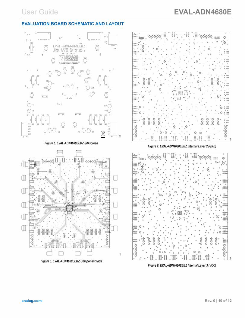
Figure 5. EVAL-ADN4680EEBZ Silkscreen
Figure 6. EVAL-ADN4680EEBZ Component Side
Figure 7. EVAL-ADN4680EEBZ Internal Layer 2 (GND)
Figure 8. EVAL-ADN4680EEBZ Internal Layer 3 (VCC)
User Guide EVAL-ADN4680EEVALUATION BOARD SCHEMATIC AND LAYOUT
analog.com Rev. 0 | 11 of 12
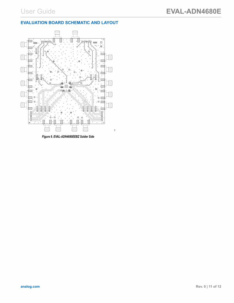
Figure 9. EVAL-ADN4680EEBZ Solder Side
User Guide EVAL-ADN4680EORDERING INFORMATION
ESD CautionESD (electrostatic discharge) sensitive device. Charged devices and circuit boards can discharge without detection. Although this product features patented or proprietaryprotection circuitry, damage may occur on devices subjected to high energy ESD. Therefore, proper ESD precautions should be taken to avoid performance degradation or loss offunctionality.
Legal Terms and ConditionsBy using the evaluation board discussed herein (together with any tools, components documentation or support materials, the “Evaluation Board”), you are agreeing to be bound by the terms andconditions set forth below (“Agreement”) unless you have purchased the Evaluation Board, in which case the Analog Devices Standard Terms and Conditions of Sale shall govern. Do not use theEvaluation Board until you have read and agreed to the Agreement. Your use of the Evaluation Board shall signify your acceptance of the Agreement. This Agreement is made by and between you(“Customer”) and Analog Devices, Inc. (“ADI”), with its principal place of business at Subject to the terms and conditions of the Agreement, ADI hereby grants to Customer a free, limited, personal,temporary, non-exclusive, non-sublicensable, non-transferable license to use the Evaluation Board FOR EVALUATION PURPOSES ONLY. Customer understands and agrees that the EvaluationBoard is provided for the sole and exclusive purpose referenced above, and agrees not to use the Evaluation Board for any other purpose. Furthermore, the license granted is expressly madesubject to the following additional limitations: Customer shall not (i) rent, lease, display, sell, transfer, assign, sublicense, or distribute the Evaluation Board; and (ii) permit any Third Party to accessthe Evaluation Board. As used herein, the term “Third Party” includes any entity other than ADI, Customer, their employees, affiliates and in-house consultants. The Evaluation Board is NOT soldto Customer; all rights not expressly granted herein, including ownership of the Evaluation Board, are reserved by ADI. CONFIDENTIALITY. This Agreement and the Evaluation Board shall all beconsidered the confidential and proprietary information of ADI. Customer may not disclose or transfer any portion of the Evaluation Board to any other party for any reason. Upon discontinuationof use of the Evaluation Board or termination of this Agreement, Customer agrees to promptly return the Evaluation Board to ADI. ADDITIONAL RESTRICTIONS. Customer may not disassemble,decompile or reverse engineer chips on the Evaluation Board. Customer shall inform ADI of any occurred damages or any modifications or alterations it makes to the Evaluation Board, includingbut not limited to soldering or any other activity that affects the material content of the Evaluation Board. Modifications to the Evaluation Board must comply with applicable law, including butnot limited to the RoHS Directive. TERMINATION. ADI may terminate this Agreement at any time upon giving written notice to Customer. Customer agrees to return to ADI the Evaluation Boardat that time. LIMITATION OF LIABILITY. THE EVALUATION BOARD PROVIDED HEREUNDER IS PROVIDED “AS IS” AND ADI MAKES NO WARRANTIES OR REPRESENTATIONS OF ANYKIND WITH RESPECT TO IT. ADI SPECIFICALLY DISCLAIMS ANY REPRESENTATIONS, ENDORSEMENTS, GUARANTEES, OR WARRANTIES, EXPRESS OR IMPLIED, RELATED TO THEEVALUATION BOARD INCLUDING, BUT NOT LIMITED TO, THE IMPLIED WARRANTY OF MERCHANTABILITY, TITLE, FITNESS FOR A PARTICULAR PURPOSE OR NONINFRINGEMENT OFINTELLECTUAL PROPERTY RIGHTS. IN NO EVENT WILL ADI AND ITS LICENSORS BE LIABLE FOR ANY INCIDENTAL, SPECIAL, INDIRECT, OR CONSEQUENTIAL DAMAGES RESULTINGFROM CUSTOMER’S POSSESSION OR USE OF THE EVALUATION BOARD, INCLUDING BUT NOT LIMITED TO LOST PROFITS, DELAY COSTS, LABOR COSTS OR LOSS OF GOODWILL.ADI’S TOTAL LIABILITY FROM ANY AND ALL CAUSES SHALL BE LIMITED TO THE AMOUNT OF ONE HUNDRED US DOLLARS ($100.00). EXPORT. Customer agrees that it will not directly orindirectly export the Evaluation Board to another country, and that it will comply with all applicable United States federal laws and regulations relating to exports. GOVERNING LAW. This Agreementshall be governed by and construed in accordance with the substantive laws of the Commonwealth of Massachusetts (excluding conflict of law rules). Any legal action regarding this Agreement willbe heard in the state or federal courts having jurisdiction in Suffolk County, Massachusetts, and Customer hereby submits to the personal jurisdiction and venue of such courts. The United NationsConvention on Contracts for the International Sale of Goods shall not apply to this Agreement and is expressly disclaimed.
©2021 Analog Devices, Inc. All rights reserved. Trademarks andregistered trademarks are the property of their respective owners.One Analog Way, Wilmington, MA 01887-2356, U.S.A.
Rev. 0 | 12 of 12
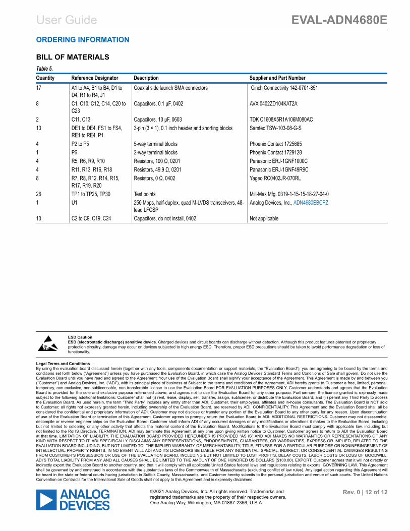
BILL OF MATERIALSTable 5.Quantity Reference Designator Description Supplier and Part Number17 A1 to A4, B1 to B4, D1 to
D4, R1 to R4, J1Coaxial side launch SMA connectors Cinch Connectivity 142-0701-851
8 C1, C10, C12, C14, C20 toC23
Capacitors, 0.1 μF, 0402 AVX 0402ZD104KAT2A
2 C11, C13 Capacitors, 10 µF, 0603 TDK C1608X5R1A106M080AC13 DE1 to DE4, FS1 to FS4,
RE1 to RE4, P13-pin (3 × 1), 0.1 inch header and shorting blocks Samtec TSW-103-08-G-S
4 P2 to P5 5-way terminal blocks Phoenix Contact 17256851 P6 2-way terminal blocks Phoenix Contact 17291284 R5, R6, R9, R10 Resistors, 100 Ω, 0201 Panasonic ERJ-1GNF1000C4 R11, R13, R16, R18 Resistors, 49.9 Ω, 0201 Panasonic ERJ-1GNF49R9C8 R7, R8, R12, R14, R15,
R17, R19, R20Resistors, 0 Ω, 0402 Yageo RC0402JR-070RL
26 TP1 to TP25, TP30 Test points Mill-Max Mfg. 0319-1-15-15-18-27-04-01 U1 250 Mbps, half-duplex, quad M-LVDS transceivers, 48-
lead LFCSPAnalog Devices, Inc., ADN4680EBCPZ
10 C2 to C9, C19, C24 Capacitors, do not install, 0402 Not applicable
Related Documents