2012 - 2015 Microchip Technology Inc. DS00001915B-page 1 Highlights • USB-IF Battery Charging 1.1 Specification Com- pliant • Link Power Management (LPM) Specification Compliant • Integrated ESD protection circuits - Up to ±25kV IEC Air Discharge without exter- nal devices • Over-Voltage Protection circuit (OVP) protects the VBUS pin from continuous DC voltages up to 30V • Microchip RapidCharge Anywhere™ Provides: - 3-times the charging current through a USB port over traditional solutions - USB-IF Battery Charging 1.1 compliance to any portable device - Charging current up to 1.5Amps via compati- ble USB host or dedicated charger - Dedicated Charging Port (DCP), Charging (CDP) & Standard (SDP) Downstream Port support • flexPWR ® Technology - Extremely low current design ideal for battery powered applications - “Sleep” mode tri-states all ULPI pins and places the part in a low current state - 1.8V to 3.3V IO Voltage • Single Power Supply Operation - Integrated 1.8V regulator - Integrated 3.3V regulator - 100mV dropout voltage • PHYBoost - Programmable USB transceiver drive strength for recovering signal integrity • VariSense TM - Programmable USB receiver sensitivity • “Wrapper-less” design for optimal timing perfor- mance and design ease - Low Latency Hi-Speed Receiver (43 Hi- Speed clocks Max) allows use of legacy UTMI Links with a ULPI bridge • External Reference Clock operation available - 19.2MHz Reference Clock needed - ULPI Clock Input Mode (60MHz sourced by Link) - 0 to 3.6V input drive tolerant - Able to accept “noisy” clock sources as refer- ence to internal, low-jitter PLL - Crystal support available • Smart detection circuits allow identification of USB charger, headset, or data cable insertion • Includes full support for the optional On-The-Go (OTG) protocol detailed in the On-The-Go Sup- plement Revision 2.0 specification • Supports the OTG Host Negotiation Protocol (HNP) and Session Request Protocol (SRP) • UART mode for non-USB serial data transfers • Internal 5V cable short-circuit protection of ID, DP and DM lines to VBUS or ground • Industrial Operating Temperature -40°C to +85°C • 32 pin, QFN RoHS Compliant package (5 x 5x 0.90 mm height) Applications The USB3370 is the solution of choice for any applica- tion where a Hi-Speed USB connection is desired and when board space, power, and interface pins must be minimized. • Cell Phones • PDAs • MP3 Players • GPS Personal Navigation • Scanners • External Hard Drives • Digital Still and Video Cameras • Portable Media Players • Entertainment Devices • Printers • Set Top Boxes • Video Record/Playback Systems • IP and Video Phones • Gaming Consoles USB3370 Enhanced Single Supply Hi-Speed USB ULPI Transceiver

Welcome message from author
This document is posted to help you gain knowledge. Please leave a comment to let me know what you think about it! Share it to your friends and learn new things together.
Transcript

USB3370Enhanced Single Supply Hi-Speed USB ULPI Transceiver
Highlights
• USB-IF Battery Charging 1.1 Specification Com-pliant
• Link Power Management (LPM) Specification Compliant
• Integrated ESD protection circuits
- Up to ±25kV IEC Air Discharge without exter-nal devices
• Over-Voltage Protection circuit (OVP) protects the VBUS pin from continuous DC voltages up to 30V
• Microchip RapidCharge Anywhere™ Provides:
- 3-times the charging current through a USB port over traditional solutions
- USB-IF Battery Charging 1.1 compliance to any portable device
- Charging current up to 1.5Amps via compati-ble USB host or dedicated charger
- Dedicated Charging Port (DCP), Charging (CDP) & Standard (SDP) Downstream Port support
• flexPWR® Technology
- Extremely low current design ideal for battery powered applications
- “Sleep” mode tri-states all ULPI pins and places the part in a low current state
- 1.8V to 3.3V IO Voltage
• Single Power Supply Operation
- Integrated 1.8V regulator
- Integrated 3.3V regulator- 100mV dropout voltage
• PHYBoost
- Programmable USB transceiver drive strength for recovering signal integrity
• VariSenseTM
- Programmable USB receiver sensitivity
• “Wrapper-less” design for optimal timing perfor-mance and design ease
- Low Latency Hi-Speed Receiver (43 Hi-Speed clocks Max) allows use of legacy UTMI Links with a ULPI bridge
• External Reference Clock operation available
- 19.2MHz Reference Clock needed
- ULPI Clock Input Mode (60MHz sourced by Link)
- 0 to 3.6V input drive tolerant
- Able to accept “noisy” clock sources as refer-ence to internal, low-jitter PLL
- Crystal support available
• Smart detection circuits allow identification of USB charger, headset, or data cable insertion
• Includes full support for the optional On-The-Go (OTG) protocol detailed in the On-The-Go Sup-plement Revision 2.0 specification
• Supports the OTG Host Negotiation Protocol (HNP) and Session Request Protocol (SRP)
• UART mode for non-USB serial data transfers
• Internal 5V cable short-circuit protection of ID, DP and DM lines to VBUS or ground
• Industrial Operating Temperature -40°C to +85°C• 32 pin, QFN RoHS Compliant package
(5 x 5x 0.90 mm height)
Applications
The USB3370 is the solution of choice for any applica-tion where a Hi-Speed USB connection is desired andwhen board space, power, and interface pins must beminimized.
• Cell Phones
• PDAs
• MP3 Players
• GPS Personal Navigation
• Scanners
• External Hard Drives
• Digital Still and Video Cameras
• Portable Media Players
• Entertainment Devices
• Printers
• Set Top Boxes
• Video Record/Playback Systems
• IP and Video Phones
• Gaming Consoles
2012 - 2015 Microchip Technology Inc. DS00001915B-page 1
USB3370
TO OUR VALUED CUSTOMERS
It is our intention to provide our valued customers with the best documentation possible to ensure successful use of your Microchipproducts. To this end, we will continue to improve our publications to better suit your needs. Our publications will be refined andenhanced as new volumes and updates are introduced.
If you have any questions or comments regarding this publication, please contact the Marketing Communications Department viaE-mail at [email protected]. We welcome your feedback.
Most Current Data SheetTo obtain the most up-to-date version of this data sheet, please register at our Worldwide Web site at:
http://www.microchip.com
You can determine the version of a data sheet by examining its literature number found on the bottom outside corner of any page. The last character of the literature number is the version number, (e.g., DS30000000A is version A of document DS30000000).
ErrataAn errata sheet, describing minor operational differences from the data sheet and recommended workarounds, may exist for cur-rent devices. As device/documentation issues become known to us, we will publish an errata sheet. The errata will specify therevision of silicon and revision of document to which it applies.
To determine if an errata sheet exists for a particular device, please check with one of the following:• Microchip’s Worldwide Web site; http://www.microchip.com• Your local Microchip sales office (see last page)
When contacting a sales office, please specify which device, revision of silicon and data sheet (include -literature number) you areusing.
Customer Notification SystemRegister on our web site at www.microchip.com to receive the most current information on all of our products.
DS00001915B-page 2 2012 - 2015 Microchip Technology Inc.
2012 - 2015 Microchip Technology Inc. DS00001915B-page 3
USB3370
Table of Contents
1.0 Introduction ..................................................................................................................................................................................... 42.0 USB3370 Pin Locations and Definitions ......................................................................................................................................... 63.0 Limiting Values ................................................................................................................................................................................ 94.0 Electrical Characteristics ............................................................................................................................................................... 105.0 Architecture Overview ................................................................................................................................................................... 176.0 ULPI Operation ............................................................................................................................................................................. 337.0 ULPI Register Map ........................................................................................................................................................................ 518.0 Application Notes .......................................................................................................................................................................... 619.0 Package Outline ............................................................................................................................................................................ 66Appendix A: Data Sheet Revision History ........................................................................................................................................... 71The Microchip Web Site ...................................................................................................................................................................... 72Customer Change Notification Service ............................................................................................................................................... 72Customer Support ............................................................................................................................................................................... 72Product Identification System ............................................................................................................................................................. 73
USB3370
1.0 INTRODUCTION
Microchip’s USB3370 is a family of Hi-Speed USB 2.0 Transceivers that provide a physical layer (PHY) solution well-suited for portable electronic devices. Both commercial and industrial temperature applications are supported.
Several advanced features make the USB3370 the transceiver of choice by reducing both eBOM part count and printedcircuit board (PCB) area. Outstanding ESD robustness eliminates the need for external ESD protection devices in typ-ical applications. The internal Over-Voltage Protection circuit (OVP) protects the USB3370 from voltages up to 30V onthe VBUS pin. By using a reference clock from the Link, the USB3370 removes the cost of a dedicated crystal referencefrom the design. The USB3370 includes integrated 3.3V and 1.8V regulators, making it possible to operate the devicefrom a single power supply.
The USB3370 is optimized for use in portable applications where a low operating current and standby currents areessential. The USB3370 operates from a single supply and includes integrated regulators for its supplies. The USB3370also supports the USB Link Power Management protocol (LPM) to further reduce USB operating currents.
The USB3370 also includes family is enabled with Microchip's RapidCharge AnywhereTM which supports USB-IF Bat-tery Charging 1.1 for any portable device. RapidCharge AnywhereTM provides three times the charging current througha USB port over traditional solutions which translate up to 1.5Amps via compatible USB host or dedicated charger. Inaddition, this provides a complete USB charging ecosystem between device and host ports such as Dedicated ChargingPort (DCP), Charging (CDP) and Standard (SDP) Downstream Ports. Section 5.9 describes this is further detail.
The USB3370 meets all of the electrical requirements for a Hi-Speed USB Host, Device, or an On-the-Go (OTG) trans-ceiver. In addition to the supporting USB signaling, the USB3370 also provides USB UART mode.
USB3370 uses the industry standard UTMI+ Low Pin Interface (ULPI) to connect the USB transceiver to the Link. ULPIuses a method of in-band signaling and status byte transfers between the Link and PHY to facilitate a USB session withonly twelve pins.
The USB3370 uses Microchip’s “wrapper-less” technology to implement the ULPI interface. This “wrapper-less” tech-nology allows the PHY to achieve a low latency transmit and receive time. Microchip’s low latency transceiver allows anexisting UTMI Link to be reused by adding a UTMI to ULPI bridge. By adding a bridge to the ASIC the existing andproven UTMI Link IP can be reused.
DS00001915B-page 4 2012 - 2015 Microchip Technology Inc.

USB3370
The USB3370 includes an integrated 3.3V LDO regulator that is used to generate 3.3V from power applied to the VBATpin. The voltage on the VBAT pin can range from 3.0 to 5.5V. The regulator dropout voltage is less than 100mV whichallows the PHY to continue USB signaling when the voltage on VBAT drops to 3.0V. The USB transceiver will continueto operate at lower voltages, although some parameters may be outside the limits of the USB specifications. The VBATand VDD33 pins should never be connected together.
In USB UART mode, the USB3370 DP and DM pins are redefined to enable pass-through of asynchronous serial data.The USB3370 will enter UART mode when programmed, as described in Section 6.7.1.
1.1 Reference Documents
UTMI+ Low Pin Interface (ULPI) Specification, Rev. 1.1
Universal Serial Bus Specification, Revision 2.0
On-The-Go Supplement to the USB2.0 Specification, Rev. 1.3
On-The-Go Supplement to the USB2.0 Specification, Rev. 2.0
USB Battery Charging Specification, Rev. 1.1
FIGURE 1-1: BLOCK DIAGRAM USB3370
OTG
Hi-Speed USB
Transceiver
ULPI Interface
ULPI Registers and State Machine
BIASLow JitterIntegrated
PLL
Integrated Power
Management
VBUS
ID
DP
DM
RBIAS
ES
D P
rote
ctio
n
RE
FC
LK /
XI
DATA[7:0]
RESETB
VDD18VDD33VBAT
DIRNXTSTP
CLKOUT
OVP
VDDIO
XO
CPEN_N
BC 1.1
EXTVBUS
2012 - 2015 Microchip Technology Inc. DS00001915B-page 5
USB3370
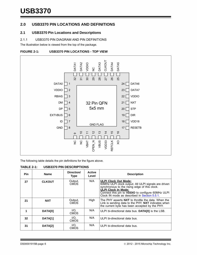
2.0 USB3370 PIN LOCATIONS AND DEFINITIONS
2.1 USB3370 Pin Locations and Descriptions
2.1.1 USB3370 PIN DIAGRAM AND PIN DEFINITIONS
The illustration below is viewed from the top of the package.
The following table details the pin definitions for the figure above.
FIGURE 2-1: USB3370 PIN LOCATIONS - TOP VIEW
TABLE 2-1: USB3370 PIN DESCRIPTIONS
Pin NameDirection/
TypeActive Level
Description
27 CLKOUT Output,CMOS
N/A ULPI Clock Out Mode:60MHz ULPI clock output. All ULPI signals are driven synchronous to the rising edge of this clock.ULPI Clock In Mode:Connect this pin to VDDIO to configure 60MHz ULPI Clock IN mode as described in Section 5.5.1.
21 NXT Output,CMOS
High The PHY asserts NXT to throttle the data. When the Link is sending data to the PHY, NXT indicates when the current byte has been accepted by the PHY.
1 DATA[0] I/O,CMOS
N/A ULPI bi-directional data bus. DATA[0] is the LSB.
32 DATA[1] I/O,CMOS
N/A ULPI bi-directional data bus.
31 DATA[2] I/O,CMOS
N/A ULPI bi-directional data bus.
USB3300Hi-Speed USB2
ULPI PHY32 Pin QFN
1
2
3
4
5
6
7
8
32 Pin QFN5x5 mm
GND FLAG
9 10 11 12 13 14 15 16
24
23
22
21
20
19
18
17
32
31
30
29
28
27
26
25
VDDIO
RBIAS
DP
EXTVBUS
DM
DATA0
VDDIO
DATA7
STP
DIR
VDD18
NXT
ID
NC
VB
US
NC
DA
TA
1
GND
VD
D33
VB
AT
CP
EN
_N
RE
FC
LK XO
RESETB
DA
TA
2
NC
DATA6V
DD
IO
DA
TA
4
CL
KO
UT
DA
TA
3
DA
TA
5
DS00001915B-page 6 2012 - 2015 Microchip Technology Inc.
USB3370
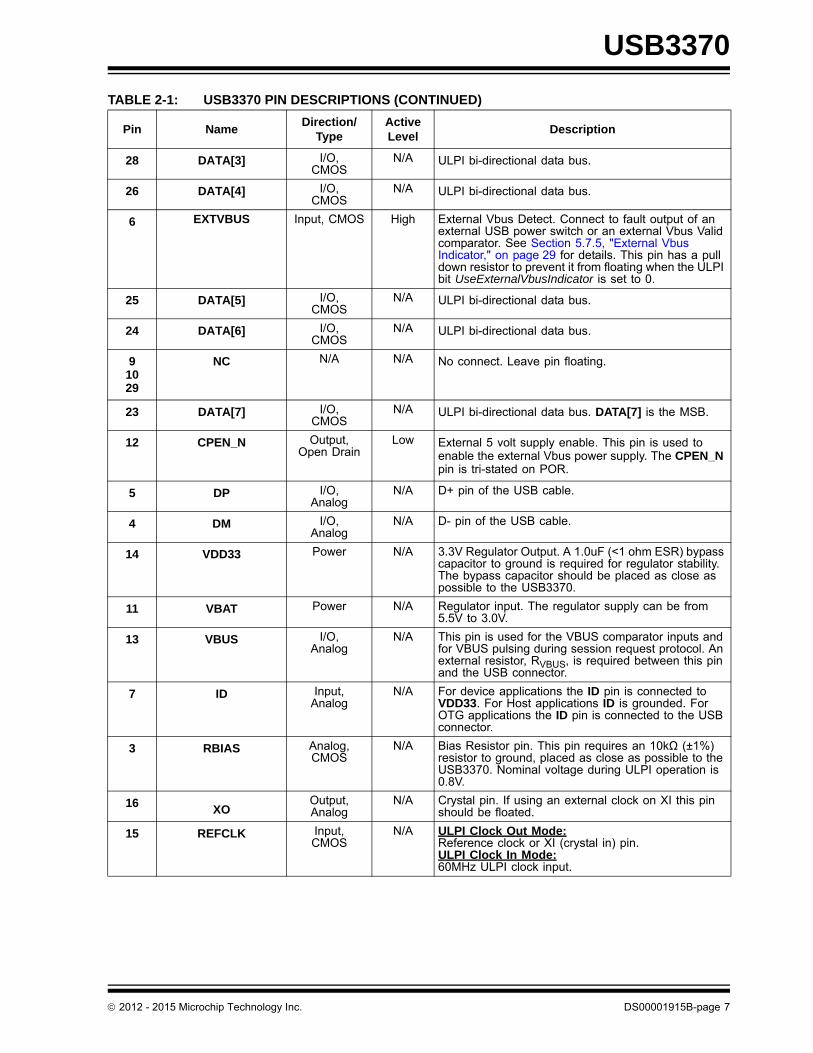
28 DATA[3] I/O,CMOS
N/A ULPI bi-directional data bus.
26 DATA[4] I/O,CMOS
N/A ULPI bi-directional data bus.
6 EXTVBUS Input, CMOS High External Vbus Detect. Connect to fault output of an external USB power switch or an external Vbus Valid comparator. See Section 5.7.5, "External Vbus Indicator," on page 29 for details. This pin has a pull down resistor to prevent it from floating when the ULPI bit UseExternalVbusIndicator is set to 0.
25 DATA[5] I/O,CMOS
N/A ULPI bi-directional data bus.
24 DATA[6] I/O,CMOS
N/A ULPI bi-directional data bus.
91029
NC N/A N/A No connect. Leave pin floating.
23 DATA[7] I/O,CMOS
N/A ULPI bi-directional data bus. DATA[7] is the MSB.
12 CPEN_N Output,Open Drain
Low External 5 volt supply enable. This pin is used to enable the external Vbus power supply. The CPEN_N pin is tri-stated on POR.
5 DP I/O,Analog
N/A D+ pin of the USB cable.
4 DM I/O,Analog
N/A D- pin of the USB cable.
14 VDD33 Power N/A 3.3V Regulator Output. A 1.0uF (<1 ohm ESR) bypass capacitor to ground is required for regulator stability. The bypass capacitor should be placed as close as possible to the USB3370.
11 VBAT Power N/A Regulator input. The regulator supply can be from 5.5V to 3.0V.
13 VBUS I/O,Analog
N/A This pin is used for the VBUS comparator inputs and for VBUS pulsing during session request protocol. An external resistor, RVBUS, is required between this pin and the USB connector.
7 ID Input,Analog
N/A For device applications the ID pin is connected to VDD33. For Host applications ID is grounded. For OTG applications the ID pin is connected to the USB connector.
3 RBIAS Analog,CMOS
N/A Bias Resistor pin. This pin requires an 10kΩ (±1%) resistor to ground, placed as close as possible to the USB3370. Nominal voltage during ULPI operation is 0.8V.
16 XOOutput,Analog
N/A Crystal pin. If using an external clock on XI this pin should be floated.
15 REFCLK Input,CMOS
N/A ULPI Clock Out Mode:Reference clock or XI (crystal in) pin.ULPI Clock In Mode:60MHz ULPI clock input.
TABLE 2-1: USB3370 PIN DESCRIPTIONS (CONTINUED)
Pin NameDirection/
TypeActive Level
Description
2012 - 2015 Microchip Technology Inc. DS00001915B-page 7

USB3370
17 RESETB Input,CMOS,
Low When low, the part is suspended and the 3.3V and 1.8V regulators are disabled. When high, the USB3370 will operate as a normal ULPI device, as described in Section 5.6.2. The state of this pin may be changed asynchronously to the clock signals. When asserted for a minimum of 1 microsecond and then de-asserted, the ULPI registers are reset to their default state and all internal state machines are reset.
18 VDD18 Power N/A 1.8V Regulator Output. A 1.0uF (<1 ohm ESR) bypass capacitor to ground is required for regulator stability. The bypass capacitor should be placed as close as possible to the USB3370.
20 STP Input,CMOS
High The Link asserts STP for one clock cycle to stop the data stream currently on the bus. If the Link is sending data to the PHY, STP indicates the last byte of data was on the bus in the previous cycle.
19 DIR Output,CMOS
N/A Controls the direction of the data bus. When the PHY has data to transfer to the Link, it drives DIR high to take ownership of the bus. When the PHY has no data to transfer it drives DIR low and monitors the bus for commands from the Link.
22230 VDDIO
Power N/A 1.8V to 3.3V ULPI interface supply voltage.
FLAG8
GND Ground N/A Ground.
TABLE 2-1: USB3370 PIN DESCRIPTIONS (CONTINUED)
Pin NameDirection/
TypeActive Level
Description
DS00001915B-page 8 2012 - 2015 Microchip Technology Inc.

2012 - 2015 Microchip Technology Inc. DS00001915B-page 9
USB3370
3.0 LIMITING VALUES
3.1 Absolute Maximum Ratings
3.2 Recommended Operating Conditions
TABLE 3-1: ABSOLUTE MAXIMUM RATINGS
Parameter Symbol Conditions MIN TYP MAX Units
VBUS, VBAT, and ID, voltage to GND
VMAX_USB Voltage measured at pin. VBUS tolerant to 30V with external RVBUS.
-0.5 6.0 V
DP and DM voltage to GND
VMAX_DPDM -0.5 5.0 V
Maximum VDD18 voltage to Ground
VMAX_18V -0.5 2.5 V
Maximum VDD33 voltage to Ground
VMAX_33V -0.5 4.0 V
Maximum VDDIO voltage to Ground
VMAX_IOV -0.5 4.0
Maximum I/O voltage to Ground
VMAX_IN -0.5 VDDIO + 0.7
Maximum I/O voltage to Ground (EXTVBUS, CPEN_N)
VMAX_IN -0.5 5.5V
Operating Temperature TMAX_OP -40 85 C
Storage Temperature TMAX_STG -55 150 C
Note: Stresses beyond those listed under “Absolute Maximum Ratings” may cause permanent damage to thedevice. Exposure to absolute maximum rating conditions for extended periods may affect device reliability.
TABLE 3-2: RECOMMENDED OPERATING CONDITIONS
Parameter Symbol Conditions MIN TYP MAX Units
VBAT to GND VBAT 3.0 5.5 V
VDD33 to GND VDD33 3.0 3.3 3.6 V
VDD18 to GND VDD18 1.6 1.8 2.0 V
VDDIO to GND VDDIO 1.6 1.8-3.3 3.6 V
Input Voltage on Digital Pins (RESETB, STP, DIR, NXT, DATA[7:0])
VI 0.0 VDDIO V
Input Voltage on Digital Pins (EXTVBUS, CPEN_N)
VI 0.0 5.0 V
Voltage on Analog I/O Pins (DP, DM, ID)
VI(I/O) 0.0 VDD33 V
VBUS to GND VVMAX 0.0 5.5
Ambient Temperature TA -40 85 C
USB3370
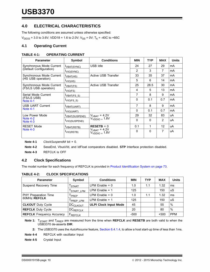
4.0 ELECTRICAL CHARACTERISTICS
The following conditions are assumed unless otherwise specified:
VDD33 = 3.0 to 3.6V; VDD18 = 1.6 to 2.0V; VSS = 0V; TA = -40C to +85C
4.1 Operating Current
Note 4-1 ClockSuspendM bit = 0.
Note 4-2 SessEnd, VbusVld, and IdFloat comparators disabled. STP Interface protection disabled.
Note 4-3 REFCLK is OFF
4.2 Clock Specifications
The model number for each frequency of REFCLK is provided in Product Identification System on page 73.
Note 1: TSTART and TPREP are measured from the time when REFCLK and RESETB are both valid to when theUSB3370 de-asserts DIR.
2: The USB3370 uses the AutoResume feature, Section 6.4.1.4, to allow a host start-up time of less than 1ms.
Note 4-4 REFCLK with oscillator Input
Note 4-5 Crystal Input
TABLE 4-1: OPERATING CURRENT
Parameter Symbol Conditions MIN TYP MAX Units
Synchronous Mode Current(Default Configuration)
IVBAT(SYNC) USB Idle 24 27 29 mA
IVIO(SYNC) 2 3 7 mA
Synchronous Mode Current(HS USB operation)
IVBAT(HS) Active USB Transfer 33 35 37 mA
IVIO(HS) 5 6 14 mA
Synchronous Mode Current(FS/LS USB operation)
IVBAT(FS) Active USB Transfer 25 28.5 30 mA
IVIO(FS) 4 5 13 mA
Serial Mode Current(FS/LS USB)Note 4-1
IVBAT(FS_S) 7 8 9 mA
IVIO(FS_S) 0 0.1 0.7 mA
USB UART CurrentNote 4-1
IVBAT(UART) 7 8 9 mA
IVIO(UART) 0 0.1 0.7 mA
Low Power ModeNote 4-2Note 4-3
IVBAT(SUSPEND) VVBAT = 4.2VVVDDIO = 1.8V
29 32 83 uA
IVIO(SUSPEND) 0 0 2 uA
RESET ModeNote 4-3
IVBAT(RSTB) RESETB = 0VVBAT = 4.2VVVDDIO = 1.8V
0.1 1 12 uA
IVIO(RSTB) 0 0 7 uA
TABLE 4-2: CLOCK SPECIFICATIONS
Parameter Symbol Conditions MIN TYP MAX Units
Suspend Recovery Time TSTART LPM Enable = 0 1.0 1.1 1.32 ms
TSTART_LPM LPM Enable = 1 125 150 uS
PHY Preparation Time60MHz REFCLK
TPREP LPM Enable = 0 1.0 1.1 1.32 ms
TPREP_LPM LPM Enable = 1 125 150 uS
CLKOUT Duty Cycle DCCLKOUT ULPI Clock Input Mode 45 55 %
REFCLK Duty Cycle DCREFCLK 20 80 %
REFCLK Frequency Accuracy FREFCLK -500 +500 PPM
DS00001915B-page 10 2012 - 2015 Microchip Technology Inc.
USB3370
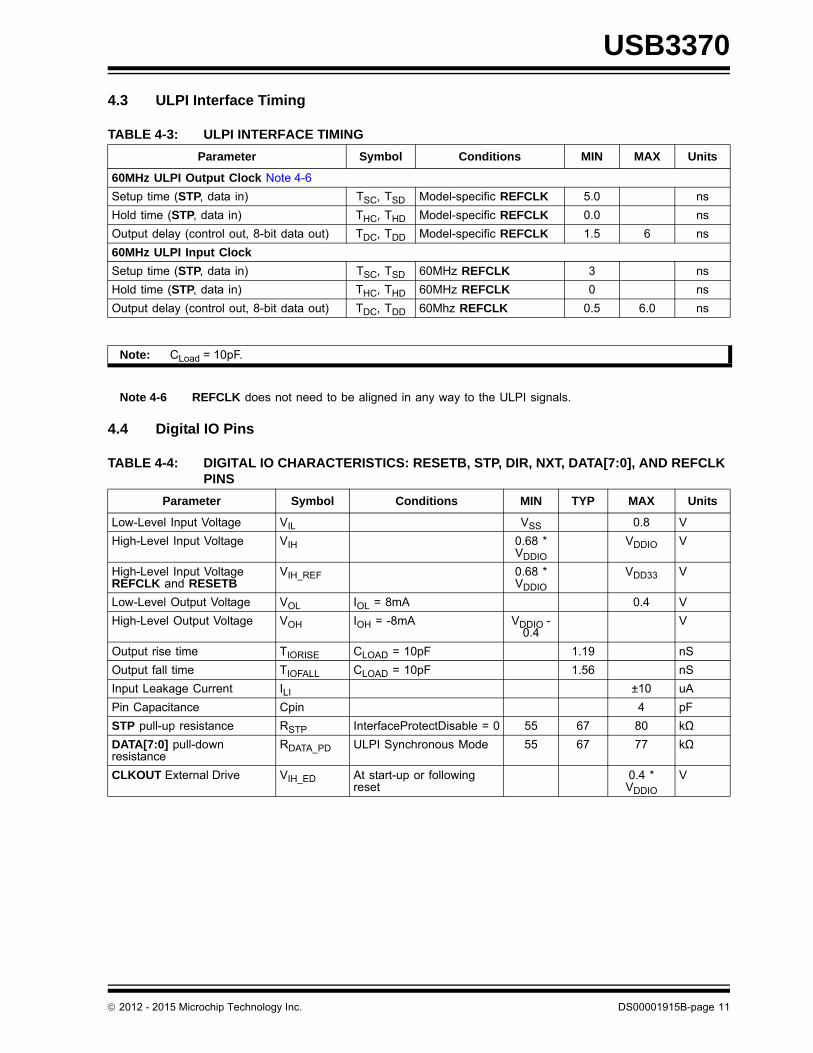
4.3 ULPI Interface Timing
Note 4-6 REFCLK does not need to be aligned in any way to the ULPI signals.
4.4 Digital IO Pins
TABLE 4-3: ULPI INTERFACE TIMING
Parameter Symbol Conditions MIN MAX Units
60MHz ULPI Output Clock Note 4-6
Setup time (STP, data in) TSC, TSD Model-specific REFCLK 5.0 ns
Hold time (STP, data in) THC, THD Model-specific REFCLK 0.0 ns
Output delay (control out, 8-bit data out) TDC, TDD Model-specific REFCLK 1.5 6 ns
60MHz ULPI Input Clock
Setup time (STP, data in) TSC, TSD 60MHz REFCLK 3 ns
Hold time (STP, data in) THC, THD 60MHz REFCLK 0 ns
Output delay (control out, 8-bit data out) TDC, TDD 60Mhz REFCLK 0.5 6.0 ns
Note: CLoad = 10pF.
TABLE 4-4: DIGITAL IO CHARACTERISTICS: RESETB, STP, DIR, NXT, DATA[7:0], AND REFCLK PINS
Parameter Symbol Conditions MIN TYP MAX Units
Low-Level Input Voltage VIL VSS 0.8 V
High-Level Input Voltage VIH 0.68 * VDDIO
VDDIO V
High-Level Input VoltageREFCLK and RESETB
VIH_REF 0.68 * VDDIO
VDD33 V
Low-Level Output Voltage VOL IOL = 8mA 0.4 V
High-Level Output Voltage VOH IOH = -8mA VDDIO - 0.4
V
Output rise time TIORISE CLOAD = 10pF 1.19 nS
Output fall time TIOFALL CLOAD = 10pF 1.56 nS
Input Leakage Current ILI ±10 uA
Pin Capacitance Cpin 4 pF
STP pull-up resistance RSTP InterfaceProtectDisable = 0 55 67 80 kΩ
DATA[7:0] pull-down resistance
RDATA_PD ULPI Synchronous Mode 55 67 77 kΩ
CLKOUT External Drive VIH_ED At start-up or following reset
0.4 *VDDIO
V
2012 - 2015 Microchip Technology Inc. DS00001915B-page 11
USB3370
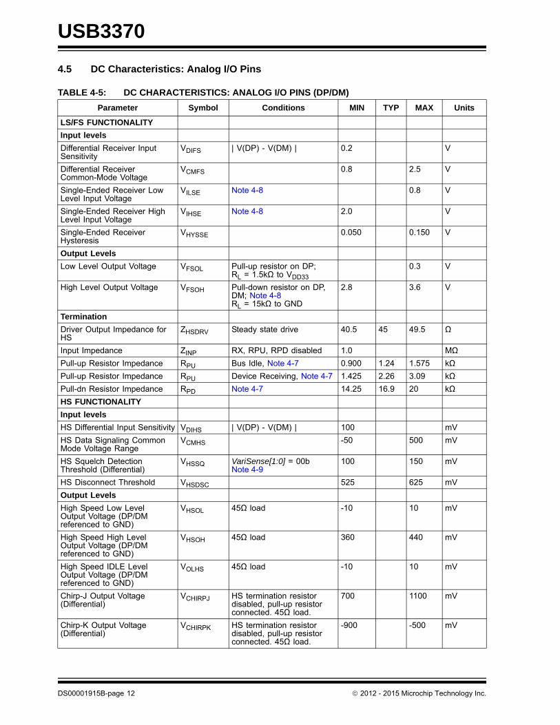
4.5 DC Characteristics: Analog I/O Pins
TABLE 4-5: DC CHARACTERISTICS: ANALOG I/O PINS (DP/DM)
Parameter Symbol Conditions MIN TYP MAX Units
LS/FS FUNCTIONALITY
Input levels
Differential Receiver Input Sensitivity
VDIFS | V(DP) - V(DM) | 0.2 V
Differential ReceiverCommon-Mode Voltage
VCMFS 0.8 2.5 V
Single-Ended Receiver Low Level Input Voltage
VILSE Note 4-8 0.8 V
Single-Ended Receiver High Level Input Voltage
VIHSE Note 4-8 2.0 V
Single-Ended Receiver Hysteresis
VHYSSE 0.050 0.150 V
Output Levels
Low Level Output Voltage VFSOL Pull-up resistor on DP;RL = 1.5kΩ to VDD33
0.3 V
High Level Output Voltage VFSOH Pull-down resistor on DP, DM; Note 4-8RL = 15kΩ to GND
2.8 3.6 V
Termination
Driver Output Impedance forHS
ZHSDRV Steady state drive 40.5 45 49.5 Ω
Input Impedance ZINP RX, RPU, RPD disabled 1.0 MΩ
Pull-up Resistor Impedance RPU Bus Idle, Note 4-7 0.900 1.24 1.575 kΩ
Pull-up Resistor Impedance RPU Device Receiving, Note 4-7 1.425 2.26 3.09 kΩ
Pull-dn Resistor Impedance RPD Note 4-7 14.25 16.9 20 kΩ
HS FUNCTIONALITY
Input levels
HS Differential Input Sensitivity VDIHS | V(DP) - V(DM) | 100 mV
HS Data Signaling CommonMode Voltage Range
VCMHS -50 500 mV
HS Squelch Detection Threshold (Differential)
VHSSQ VariSense[1:0] = 00bNote 4-9
100 150 mV
HS Disconnect Threshold VHSDSC 525 625 mV
Output Levels
High Speed Low LevelOutput Voltage (DP/DMreferenced to GND)
VHSOL 45Ω load -10 10 mV
High Speed High LevelOutput Voltage (DP/DMreferenced to GND)
VHSOH 45Ω load 360 440 mV
High Speed IDLE LevelOutput Voltage (DP/DMreferenced to GND)
VOLHS 45Ω load -10 10 mV
Chirp-J Output Voltage (Differential)
VCHIRPJ HS termination resistor disabled, pull-up resistor connected. 45Ω load.
700 1100 mV
Chirp-K Output Voltage(Differential)
VCHIRPK HS termination resistor disabled, pull-up resistor connected. 45Ω load.
-900 -500 mV
DS00001915B-page 12 2012 - 2015 Microchip Technology Inc.
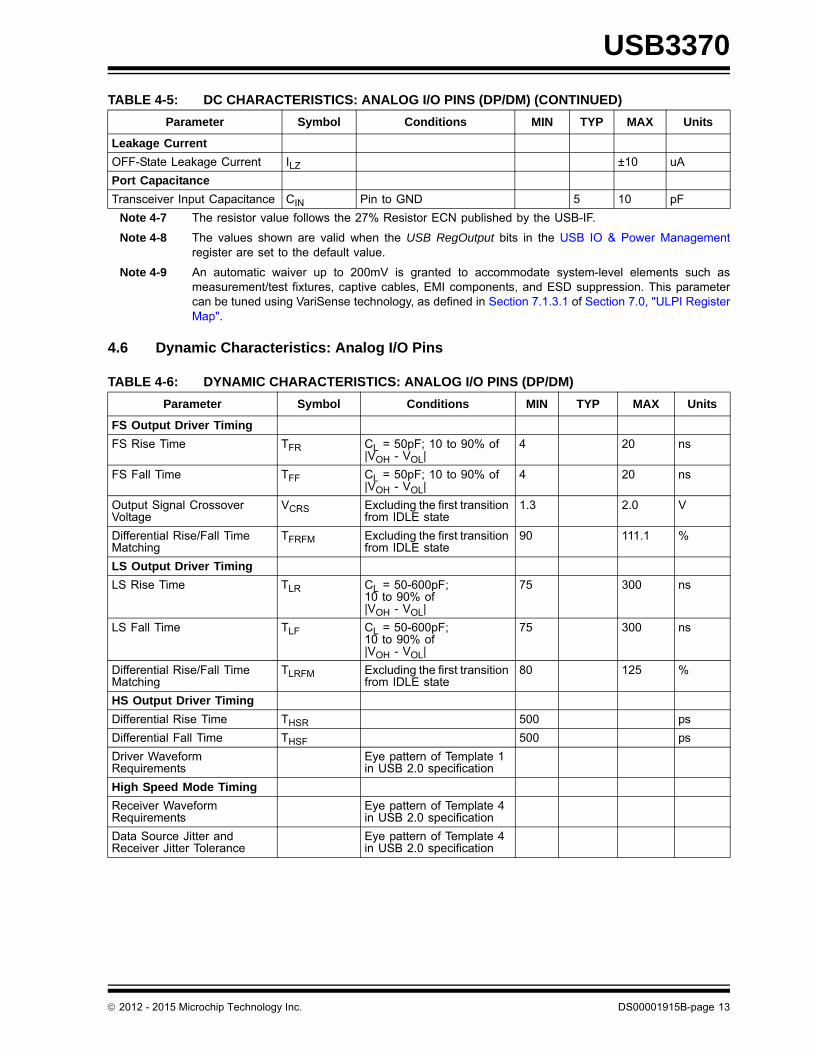
USB3370
Note 4-7 The resistor value follows the 27% Resistor ECN published by the USB-IF.
Note 4-8 The values shown are valid when the USB RegOutput bits in the USB IO & Power Managementregister are set to the default value.
Note 4-9 An automatic waiver up to 200mV is granted to accommodate system-level elements such asmeasurement/test fixtures, captive cables, EMI components, and ESD suppression. This parametercan be tuned using VariSense technology, as defined in Section 7.1.3.1 of Section 7.0, "ULPI RegisterMap".
4.6 Dynamic Characteristics: Analog I/O Pins
Leakage Current
OFF-State Leakage Current ILZ ±10 uA
Port Capacitance
Transceiver Input Capacitance CIN Pin to GND 5 10 pF
TABLE 4-6: DYNAMIC CHARACTERISTICS: ANALOG I/O PINS (DP/DM)
Parameter Symbol Conditions MIN TYP MAX Units
FS Output Driver Timing
FS Rise Time TFR CL = 50pF; 10 to 90% of|VOH - VOL|
4 20 ns
FS Fall Time TFF CL = 50pF; 10 to 90% of|VOH - VOL|
4 20 ns
Output Signal Crossover Voltage
VCRS Excluding the first transition from IDLE state
1.3 2.0 V
Differential Rise/Fall Time Matching
TFRFM Excluding the first transition from IDLE state
90 111.1 %
LS Output Driver Timing
LS Rise Time TLR CL = 50-600pF;10 to 90% of|VOH - VOL|
75 300 ns
LS Fall Time TLF CL = 50-600pF;10 to 90% of|VOH - VOL|
75 300 ns
Differential Rise/Fall Time Matching
TLRFM Excluding the first transition from IDLE state
80 125 %
HS Output Driver Timing
Differential Rise Time THSR 500 ps
Differential Fall Time THSF 500 ps
Driver Waveform Requirements
Eye pattern of Template 1 in USB 2.0 specification
High Speed Mode Timing
Receiver Waveform Requirements
Eye pattern of Template 4 in USB 2.0 specification
Data Source Jitter and Receiver Jitter Tolerance
Eye pattern of Template 4 in USB 2.0 specification
TABLE 4-5: DC CHARACTERISTICS: ANALOG I/O PINS (DP/DM) (CONTINUED)
Parameter Symbol Conditions MIN TYP MAX Units
2012 - 2015 Microchip Technology Inc. DS00001915B-page 13
USB3370
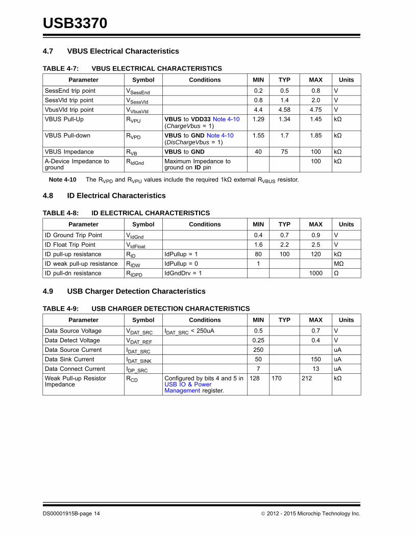
4.7 VBUS Electrical Characteristics
Note 4-10 The RVPD and RVPU values include the required 1kΩ external RVBUS resistor.
4.8 ID Electrical Characteristics
4.9 USB Charger Detection Characteristics
TABLE 4-7: VBUS ELECTRICAL CHARACTERISTICS
Parameter Symbol Conditions MIN TYP MAX Units
SessEnd trip point VSessEnd 0.2 0.5 0.8 V
SessVld trip point VSessVld 0.8 1.4 2.0 V
VbusVld trip point VVbusVld 4.4 4.58 4.75 V
VBUS Pull-Up RVPU VBUS to VDD33 Note 4-10(ChargeVbus = 1)
1.29 1.34 1.45 kΩ
VBUS Pull-down RVPD VBUS to GND Note 4-10(DisChargeVbus = 1)
1.55 1.7 1.85 kΩ
VBUS Impedance RVB VBUS to GND 40 75 100 kΩ
A-Device Impedance to ground
RIdGnd Maximum Impedance to ground on ID pin
100 kΩ
TABLE 4-8: ID ELECTRICAL CHARACTERISTICS
Parameter Symbol Conditions MIN TYP MAX Units
ID Ground Trip Point VIdGnd 0.4 0.7 0.9 V
ID Float Trip Point VIdFloat 1.6 2.2 2.5 V
ID pull-up resistance RID IdPullup = 1 80 100 120 kΩ
ID weak pull-up resistance RIDW IdPullup = 0 1 MΩ
ID pull-dn resistance RIDPD IdGndDrv = 1 1000 Ω
TABLE 4-9: USB CHARGER DETECTION CHARACTERISTICS
Parameter Symbol Conditions MIN TYP MAX Units
Data Source Voltage VDAT_SRC IDAT_SRC < 250uA 0.5 0.7 V
Data Detect Voltage VDAT_REF 0.25 0.4 V
Data Source Current IDAT_SRC 250 uA
Data Sink Current IDAT_SINK 50 150 uA
Data Connect Current IDP_SRC 7 13 uA
Weak Pull-up Resistor Impedance
RCD Configured by bits 4 and 5 in USB IO & Power Management register.
128 170 212 kΩ
DS00001915B-page 14 2012 - 2015 Microchip Technology Inc.

USB3370
4.10 Regulator Output Voltages and Capacitor Requirement
4.11 Piezoelectric Resonator for Internal Oscillator
The internal oscillator may be used with an external quartz crystal or ceramic resonator as described in Section 5.4. SeeTable 4-11 for the recommended crystal specifications.
Note 4-11 The required bit rate accuracy for Hi-Speed USB applications is ±500 ppm as provided in the USB2.0 Specification. This takes into account the effect of voltage, temperature, aging, etc.
Note 4-12 This number includes the pad, the bond wire and the lead frame. Printed Circuit Board (PCB)capacitance is not included in this value. The PCB capacitance value and the capacitance value ofthe XO and REFCLK pins are required to accurately calculate the value of the two external loadcapacitors.
Note 4-13 Refer to Section 5.4 and Figure 8-1 for more information.
TABLE 4-10: REGULATOR OUTPUT VOLTAGES AND CAPACITOR REQUIREMENT
Parameter Symbol Conditions MIN TYP MAX Units
Regulator Output Voltage VDD33 5.5V > VBAT > 3.0V 2.8 3.3 3.6 V
USB UART Mode & UART RegOutput[1:0] = 016V > VBAT > 3.0V
2.7 3.0 3.3 V
USB UART Mode & UART RegOutput[1:0] = 106V > VBAT > 3.0V
2.47 2.75 3.03 V
USB UART Mode & UART RegOutput[1:0] = 116V > VBAT > 3.0V
2.25 2.5 2.75 V
Regulator Bypass Capacitor COUT33 1.0 uF
Bypass Capacitor ESR CESR33 1 Ω
Regulator Output Voltage VDD18 3.6V > VDD33 > 2.25V 1.6 1.8 2.0 V
Regulator Bypass Capacitor COUT18 1.0 uF
Bypass Capacitor ESR CESR18 1 Ω
TABLE 4-11: USB3370 QUARTZ CRYSTAL SPECIFICATIONS
Parameter Symbol MIN NOM MAX Units Notes
Crystal Cut AT, typ
Crystal Oscillation Mode Fundamental Mode
Crystal Calibration Mode Parallel Resonant Mode
Frequency Ffund - See Product Identification System on
page 73
- MHz
Total Allowable PPM Budget - - ±500 PPM Note 4-11
Shunt Capacitance CO - 7 typ - pF
Load Capacitance CL - 20 typ - pF
Drive Level PW 0.1 - - mW
Equivalent Series Resistance R1 - - 30 Ohm
USB3370 REFCLK Pin Capacitance
- 3 typ - pF Note 4-12
USB3370 XO Pin Capacitance - 3 typ - pF Note 4-12
Recommended Resistance between XI and XO
1M - - Ohm Note 4-13
2012 - 2015 Microchip Technology Inc. DS00001915B-page 15
USB3370
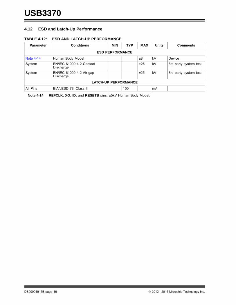
4.12 ESD and Latch-Up Performance
Note 4-14 REFCLK, XO, ID, and RESETB pins: ±5kV Human Body Model.
TABLE 4-12: ESD AND LATCH-UP PERFORMANCE
Parameter Conditions MIN TYP MAX Units Comments
ESD PERFORMANCE
Note 4-14 Human Body Model ±8 kV Device
System EN/IEC 61000-4-2 Contact Discharge
±25 kV 3rd party system test
System EN/IEC 61000-4-2 Air-gap Discharge
±25 kV 3rd party system test
LATCH-UP PERFORMANCE
All Pins EIA/JESD 78, Class II 150 mA
DS00001915B-page 16 2012 - 2015 Microchip Technology Inc.

USB3370
5.0 ARCHITECTURE OVERVIEW
The USB3370 consists of the blocks shown in the diagram below.
5.1 ULPI Digital Operation and Interface
This section of the USB3370 is covered in detail in Section 6.0, "ULPI Operation".
5.2 USB 2.0 Hi-Speed Transceiver
The blocks in the lower left-hand corner of Figure 6-1 interface to the DP/DM pins.
5.2.1 USB TRANSCEIVER
The USB3370 transceiver includes a Universal Serial Bus Specification Rev 2.0 compliant receiver and transmitter. TheDP/DM signals in the USB cable connect directly to the receivers and transmitters.
The receiver consists of receivers for HS and FS/LS mode. Depending on the mode, the selected receiver provides theserial data stream through the multiplexer to the RX Logic block. For HS mode support, the HS RX block contains asquelch circuit to insure that noise is not interpreted as data. The RX block also includes a single-ended receiver oneach of the data lines to determine the correct FS linestate.
Data from the Link is encoded, bit stuffed, serialized and transmitted onto the USB cable by the transmitter. Separatedifferential FS/LS and HS transmitters are included to support all modes.
The USB3370 TX block meets the HS signaling level requirements in the USB 2.0 Specification when the PCB tracesfrom the DP and DM pins to the USB connector are correctly designed. In some systems the proper 90 ohm differentialimpedance can not be maintained and it may be desirable to compensate for loss by adjusting the HS transmitter ampli-tude and this HS squelch threshold. The PHYBoost bits in the HS Compensation Register may be configured to adjustthe HS transmitter amplitude at the DP and DM pins. The VariSense bits in the HS Compensation Register can also beused to lower the squelch threshold to compensate for losses on the PCB.
To ensure proper operation of the USB transceiver the settings of Table 5-1 must be followed.
FIGURE 5-1: USB3370 SYSTEM DIAGRAM
BIAS
Integrated Low Jitter
PLL
RBIAS
ES
D P
rote
ctio
n
RC
D
RC
D
RP
D
RP
D
RP
U
RP
UR
ID
RID
W
RV
PU
RV
B
DIRNXTSTP
CLKOUT
DATA7DATA6DATA5DATA4DATA3DATA2
DATA0DATA1
REFCLK / XI
VDDIO
VBAT
VDD33
VBUS
LDO
DP
DM
ID ULPI Digitial
Dig
ital I
O
OT
G M
odul
eTX
RX
HS/FS/LSTX Encoding
HS/FS/LSRX Decoding
RESETB
TX
Dat
a
RX
Dat
a
IdGnd
IdFloat
Rid Value
SessEnd
SessValid
VbusValid
RV
PD
OVP
XO
CPEN_N
VDD33
VDD33
VDD33
LDOVDD18
EXTVBUS
2012 - 2015 Microchip Technology Inc. DS00001915B-page 17

USB3370
5.2.2 TERMINATION RESISTORS
The USB3370 transceiver fully integrates all of the USB termination resistors on both DP and DM. This includes 1.5kΩpull-up resistors, 15kΩ pull-down resistors and the 45Ω High Speed termination resistors. These resistors require notuning or trimming by the Link. The state of the resistors is determined by the operating mode of the transceiver whenoperating in synchronous mode.
The XcvrSelect[1:0], TermSelect and OpMode[1:0] bits in the Function Control register, and the DpPulldown andDmPulldown bits in the OTG Control register control the configuration of the termination resistors. All possible validresistor combinations are shown in Table 5-1, and operation is ensured in only the configurations shown. If a ULPI Reg-ister Setting is configured that does not match a setting in the table, the transceiver operation is not guaranteed and thesettings in the last row of Table 5-1 will be used.
• RPU_DP_EN activates the 1.5kΩ DP pull-up resistor
• RPU_DM_EN activates the 1.5kΩ DM pull-up resistor
• RPD_DP_EN activates the 15kΩ DP pull-down resistor
• RPD_DM_EN activates the 15kΩ DM pull-down resistor
• HSTERM_EN activates the 45Ω DP and DM High Speed termination resistors
TABLE 5-1: DP/DM TERMINATION VS. SIGNALING MODE
Signaling Mode
ULPI Register SettingsUSB3370 Termination Resistor
Settings
Xc
vrS
elec
t[1:
0]
Ter
mS
ele
ct
Op
Mo
de[
1:0]
Dp
Pu
lldo
wn
Dm
Pu
lldo
wn
RP
U_D
P_E
N
RP
U_D
M_
EN
RP
D_
DP
_EN
RP
D_D
M_E
N
HS
TE
RM
_E
N
General Settings
Tri-State Drivers, Note 5-1 XXb Xb 01b Xb Xb 0b 0b 0b 0b 0b
Power-up or VBUS < VSESSEND 01b 0b 00b 1b 1b 0b 0b 1b 1b 0b
Host Settings
Host Chirp 00b 0b 10b 1b 1b 0b 0b 1b 1b 1b
Host High Speed 00b 0b 00b 1b 1b 0b 0b 1b 1b 1b
Host Full Speed X1b 1b 00b 1b 1b 0b 0b 1b 1b 0b
Host HS/FS Suspend 01b 1b 00b 1b 1b 0b 0b 1b 1b 0b
Host HS/FS Resume 01b 1b 10b 1b 1b 0b 0b 1b 1b 0b
Host Low Speed 10b 1b 00b 1b 1b 0b 0b 1b 1b 0b
Host LS Suspend 10b 1b 00b 1b 1b 0b 0b 1b 1b 0b
Host LS Resume 10b 1b 10b 1b 1b 0b 0b 1b 1b 0b
Host Test J/Test_K 00b 0b 10b 1b 1b 0b 0b 1b 1b 1b
Peripheral Settings
Peripheral Chirp 00b 1b 10b 0b 0b 1b 0b 0b 0b 0b
Peripheral HS 00b 0b 00b 0b 0b 0b 0b 0b 0b 1b
Peripheral FS 01b 1b 00b 0b 0b 1b 0b 0b 0b 0b
Peripheral HS/FS Suspend 01b 1b 00b 0b 0b 1b 0b 0b 0b 0b
Peripheral HS/FS Resume 01b 1b 10b 0b 0b 1b 0b 0b 0b 0b
Peripheral LS 10b 1b 00b 0b 0b 0b 1b 0b 0b 0b
Peripheral LS Suspend 10b 1b 00b 0b 0b 0b 1b 0b 0b 0b
Peripheral LS Resume 10b 1b 10b 0b 0b 0b 1b 0b 0b 0b
Peripheral Test J/Test K 00b 0b 10b 0b 0b 0b 0b 0b 0b 1b
OTG device, Peripheral Chirp 00b 1b 10b 0b 1b 1b 0b 0b 1b 0b
OTG device, Peripheral HS 00b 0b 00b 0b 1b 0b 0b 0b 1b 1b
DS00001915B-page 18 2012 - 2015 Microchip Technology Inc.
USB3370
Note 1: This is equivalent to Table 40, Section 4.4 of the ULPI 1.1 specification.
2: USB3370 does not support operation as an upstream hub port. See Section 6.4.1.3.
Note 5-1 When RESETB = 0 The HS termination will tri-state the USB drivers
Note 5-2 The transceiver operation is not guaranteed in a combination that is not defined.
The USB3370 uses the 27% resistor ECN resistor tolerances. The resistor values are shown in Table 4-5.
5.3 Bias Generator
This block consists of an internal bandgap reference circuit used for generating the driver current and the biasing of theanalog circuits. This block requires an external 10KΩ, 1% tolerance, reference resistor connected from RBIAS toground. This resistor should be placed as close as possible to the USB3370 to minimize the trace length. The nominalvoltage at RBIAS is 0.8V +/- 10% and therefore the resistor will dissipate approximately 80μW of power.
5.4 Crystal Reference Support
The USB3370 provides support for a crystal to provide the reference frequency required by the device in place of a clockoscillator. The crystal should be connected to the REFCLK/XI and XO pins. If a clock oscillator is used in place of acrystal, it should be driven into the REFCLK/XI pin, and the XO pin should be left floating. Proper care should be takento ensure that a crystal is selected with appropriate power dissipation characteristics.
5.5 Integrated Low Jitter PLL
The USB3370 uses an integrated low jitter phase locked loop (PLL) to provide a clean 480MHz clock required for HSUSB signal quality. This clock is used by the PHY during both transmit and receive. The USB3370 PLL requires an accu-rate frequency reference to be driven on the REFCLK pin.
5.5.1 REFCLK FREQUENCY SELECTION
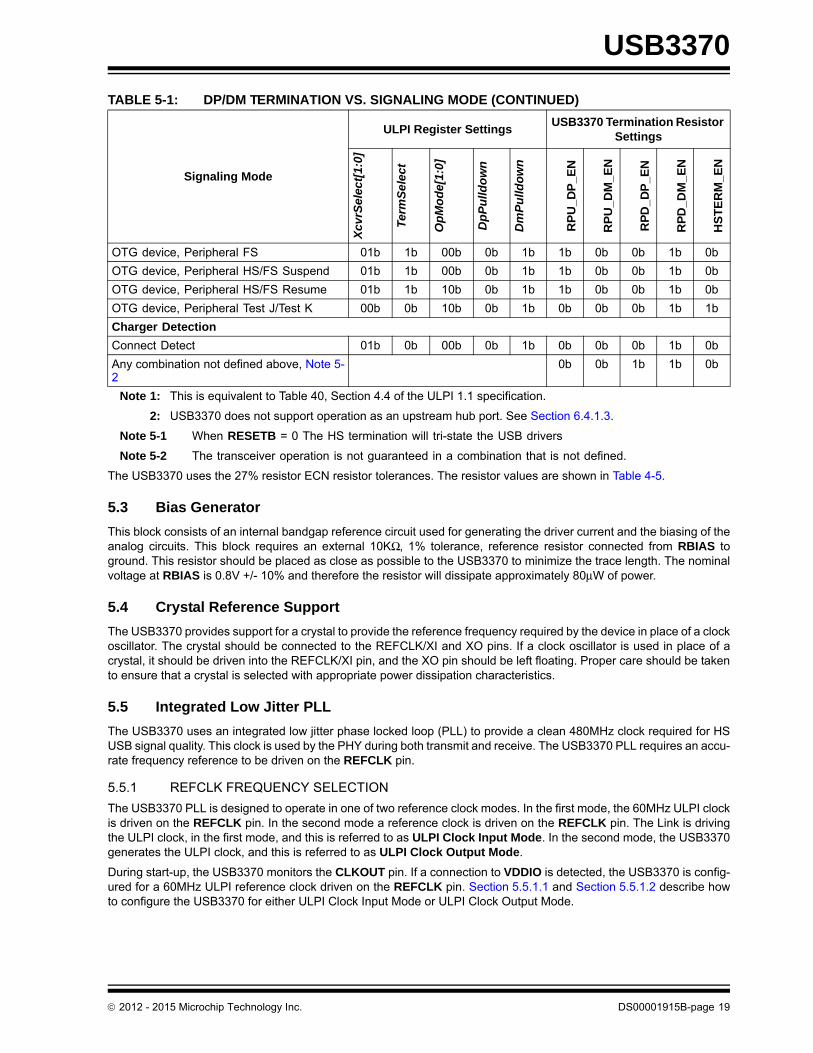
The USB3370 PLL is designed to operate in one of two reference clock modes. In the first mode, the 60MHz ULPI clockis driven on the REFCLK pin. In the second mode a reference clock is driven on the REFCLK pin. The Link is drivingthe ULPI clock, in the first mode, and this is referred to as ULPI Clock Input Mode. In the second mode, the USB3370generates the ULPI clock, and this is referred to as ULPI Clock Output Mode.
During start-up, the USB3370 monitors the CLKOUT pin. If a connection to VDDIO is detected, the USB3370 is config-ured for a 60MHz ULPI reference clock driven on the REFCLK pin. Section 5.5.1.1 and Section 5.5.1.2 describe howto configure the USB3370 for either ULPI Clock Input Mode or ULPI Clock Output Mode.
OTG device, Peripheral FS 01b 1b 00b 0b 1b 1b 0b 0b 1b 0b
OTG device, Peripheral HS/FS Suspend 01b 1b 00b 0b 1b 1b 0b 0b 1b 0b
OTG device, Peripheral HS/FS Resume 01b 1b 10b 0b 1b 1b 0b 0b 1b 0b
OTG device, Peripheral Test J/Test K 00b 0b 10b 0b 1b 0b 0b 0b 1b 1b
Charger Detection
Connect Detect 01b 0b 00b 0b 1b 0b 0b 0b 1b 0b
Any combination not defined above, Note 5-2
0b 0b 1b 1b 0b
TABLE 5-1: DP/DM TERMINATION VS. SIGNALING MODE (CONTINUED)
Signaling Mode
ULPI Register SettingsUSB3370 Termination Resistor
Settings
Xcv
rSel
ect[
1:0]
Ter
mS
ele
ct
Op
Mo
de[
1:0]
Dp
Pu
lldo
wn
Dm
Pu
lldo
wn
RP
U_D
P_E
N
RP
U_D
M_
EN
RP
D_D
P_E
N
RP
D_D
M_
EN
HS
TE
RM
_E
N
2012 - 2015 Microchip Technology Inc. DS00001915B-page 19

USB3370
5.5.1.1 ULPI Clock Input Mode (60MHz REFCLK Mode)
When using ULPI Clock Input Mode, the Link must supply the 60MHz ULPI clock to the USB3370. In this mode the60MHz ULPI Clock is connected to the REFCLK pin, and the CLKOUT pin is tied high to VDDIO.
After the PLL has locked to the correct frequency, the USB3370 will de-assert DIR and the Link can begin using theULPI interface. The USB3370 is ensured to start the clock within the time specified in Table 4-2. For Host applications,the ULPI AutoResume bit should be enabled. This is described in Section 6.4.1.4.
For the USB3370, the REF pins should be tied to ground.
5.5.1.2 ULPI Clock Output Mode
When using ULPI Clock Output Mode, the USB3370 generates the 60MHz ULPI clock used by the Link. In this mode,the REFCLK pin must be driven with the model-specific frequency, and the CLKOUT pin sources the 60MHz ULPI clockto the Link. When using ULPI Clock Output Mode, the system must not drive the CLKOUT pin following POR or hard-ware reset with a voltage that exceeds the value of VIH_ED provided in Table 4-3. An example of ULPI Clock OutputMode is shown in Figure 8-1
After the PLL has locked to the correct frequency, the USB3370 generates the 60MHz ULPI clock on the CLKOUT pin,and de-asserts DIR to indicate that the PLL is locked. The USB3370 is ensured to start the clock within the time specifiedin Table 4-2, and it will be accurate to within ±500ppm. For Host applications the ULPI AutoResume bit should beenabled. This is described in Section 6.4.1.4.
When using ULPI Clock Output Mode, the edges of the reference clock do not need to be aligned in any way to the ULPIinterface signals. There is no need to align the phase of the REFCLK and the CLKOUT.
FIGURE 5-2: CONFIGURING THE USB3370 FOR ULPI CLOCK INPUT MODE (60 MHZ)
CLKOUT
REFCLK
~~
~~ PHYClock
Source
To PLLLink
ULPI Clk Out
Reference Clk In
VDD18/VDDIO
DS00001915B-page 20 2012 - 2015 Microchip Technology Inc.
USB3370
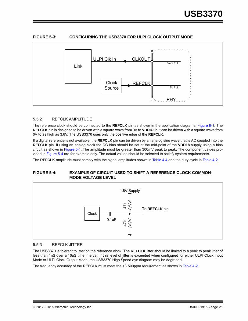
5.5.2 REFCLK AMPLITUDE
The reference clock should be connected to the REFCLK pin as shown in the application diagrams, Figure 8-1. TheREFCLK pin is designed to be driven with a square wave from 0V to VDDIO, but can be driven with a square wave from0V to as high as 3.6V. The USB3370 uses only the positive edge of the REFCLK.
If a digital reference is not available, the REFCLK pin can be driven by an analog sine wave that is AC coupled into theREFCLK pin. If using an analog clock the DC bias should be set at the mid-point of the VDD18 supply using a biascircuit as shown in Figure 5-4. The amplitude must be greater than 300mV peak to peak. The component values pro-vided in Figure 5-4 are for example only. The actual values should be selected to satisfy system requirements.
The REFCLK amplitude must comply with the signal amplitudes shown in Table 4-4 and the duty cycle in Table 4-2.
5.5.3 REFCLK JITTER
The USB3370 is tolerant to jitter on the reference clock. The REFCLK jitter should be limited to a peak to peak jitter ofless than 1nS over a 10uS time interval. If this level of jitter is exceeded when configured for either ULPI Clock InputMode or ULPI Clock Output Mode, the USB3370 High Speed eye diagram may be degraded.
The frequency accuracy of the REFCLK must meet the +/- 500ppm requirement as shown in Table 4-2.
FIGURE 5-3: CONFIGURING THE USB3370 FOR ULPI CLOCK OUTPUT MODE
FIGURE 5-4: EXAMPLE OF CIRCUIT USED TO SHIFT A REFERENCE CLOCK COMMON-MODE VOLTAGE LEVEL
CLKOUT
REFCLK
~~
~~ PHY
From PLL
ClockSource To PLL
Link
ULPI Clk In
Clock
47k
47k
0.1uF
1.8V Supply
To REFCLK pin
2012 - 2015 Microchip Technology Inc. DS00001915B-page 21

USB3370
5.5.4 REFCLK ENABLE/DISABLE
The REFCLK should be enabled when the RESETB pin is brought high. The ULPI interface will start running after thetime specified in Table 4-2. If the reference clock enable is delayed relative to the RESETB pin, the ULPI interface willstart operation delayed by the same amount. The reference clock can be run at anytime the RESETB pin is low withoutcausing the USB3370 to start-up or draw current.
When the USB3370 is placed in Low Power Mode or Carkit Mode, the reference clock can be stopped after the finalULPI register write is complete. The STP pin is asserted to bring the USB3370 out of Low Power Mode. The referenceclock should be started at the same time STP is asserted to minimize the USB3370 start-up time.
If the reference clock is stopped while in ULPI Synchronous mode the PLL will come out of lock and the frequency ofoscillation will decrease to the minimum allowed by the PLL design. If the reference clock is stopped during a USB ses-sion, the session may drop.
5.6 Internal Regulators and POR
The USB3370 includes integrated power management functions, including a Low-Dropout regulator that can be usedto generate the 3.3V USB supply, an integrated 1.8V regulator, and a POR generator described in Section 5.6.2.
5.6.1 INTEGRATED LOW DROPOUT REGULATORS
The USB3370 includes two integrated linear regulators. Power sourced at the VBAT pin is regulated to 3.3V and 1.8Voutput on the VDD33 and VDD18 pins. To ensure stability, both regulators require an external bypass capacitor as spec-ified in Table 4-10 placed as close to the pin as possible.
The USB3370 regulators are designed to generate the 3.3 Volt and 1.8 Volt supplies for the USB3370 only. Using theregulators to provide current for other circuits is not recommended and Microchip does not guarantee USB performanceor regulator stability.
During USB UART mode the 3.3V regulator output voltage can be changed to allow the USB3370 to work with UARTsoperating at different operating voltages. The 3.3V regulator output is configured to the voltages shown in Table 4-10with the UART RegOutput[1:0] bits in the USB IO & Power Management register.
The regulators are enabled by the RESETB pin. When RESETB pin is low both regulators are disabled and the regulatoroutputs are pulled low by weak pull-down. The RESETB pin must be brought high to enable the regulators.
For peripheral-only or host-only bus-powered applications, the input to VBAT may be derived from the VBUS pin of theUSB connector. In this configuration, the supply must be capable of withstanding any transient voltage present at theVBUS pin of the USB connector. Microchip does not recommend connecting the VBAT pin to the VBUS terminal of theUSB connector.
5.6.2 POWER ON RESET (POR)
The USB3370 provides a POR circuit that generates an internal reset pulse after the VDD18 supply is stable. After theinternal POR goes high the USB3370 will release from reset and begin normal ULPI operation as described inSection 5.6.4.
The ULPI registers will power up in their default state summarized in Table 7-1 when the 1.8V supply comes up. Cyclingthe RESETB pin can also be used to reset the ULPI registers to their default state (and reset all internal state machines)by bringing the pin low for a minimum of 1 microsecond and then high. It is not necessary to wait for the VDD33 andVDD18 pins to discharge to 0 volts to reset the part.
The RESETB pin must be pulled high to enable the 3.3V and 1.8V regulators. A pull-down resistor is not present on theRESETB pin and therefore the system should drive the RESETB pin to the desired state at all times. If the system doesnot need to place the USB3370 into reset mode the RESETB pin can be connected to a supply between 1.8V and 3.3V.
5.6.3 RECOMMENDED POWER SUPPLY SEQUENCE
For USB operation, the USB3370 requires a valid voltage on the VBAT and VDDIO pins. The VDD33 and VDD18 reg-ulators are automatically enabled when the RESETB pin is brought high. For the USB3343, Table 5-2 presents thepower supply configurations in more detail.
The RESETB pin can be held low until the VBAT supply is stable. If the Link is not ready to interface the USB3370, theLink may choose to hold the RESETB pin low until it is ready to control the ULPI interface.
DS00001915B-page 22 2012 - 2015 Microchip Technology Inc.
USB3370
Note 5-3 VDDIO must be present for ULPI pins to tri-state.
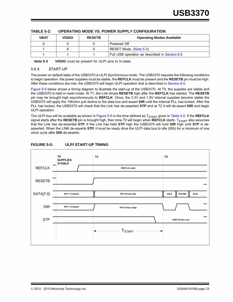
5.6.4 START-UP
The power on default state of the USB3370 is ULPI Synchronous mode. The USB3370 requires the following conditionsto begin operation: the power supplies must be stable, the REFCLK must be present and the RESETB pin must be high.After these conditions are met, the USB3370 will begin ULPI operation that is described in Section 6.0.
Figure 5-5 below shows a timing diagram to illustrate the start-up of the USB3370. At T0, the supplies are stable andthe USB3370 is held in reset mode. At T1, the Link drives RESETB high after the REFCLK has started. The RESETBpin may be brought high asynchronously to REFCLK. Once, the 3.3V and 1.8V internal supplies become stable theUSB3370 will apply the 15Kohm pull downs to the data bus and assert DIR until the internal PLL has locked. After thePLL has locked, the USB3370 will check that the Link has de-asserted STP and at T2 it will de-assert DIR and beginULPI operation.
The ULPI bus will be available as shown in Figure 5-5 in the time defined as TSTART given in Table 4-2. If the REFCLKsignal starts after the RESETB pin is brought high, then time T0 will begin when REFCLK starts. TSTART also assumesthat the Link has de-asserted STP. If the Link has held STP high the USB3370 will hold DIR high until STP is de-asserted. When the LINK de-asserts STP, it must be ready drive the ULPI data bus to idle (00h) for a minimum of oneclock cycle after DIR de-asserts.
TABLE 5-2: OPERATING MODE VS. POWER SUPPLY CONFIGURATION
VBAT VDDIO RESETB Operating Modes Available
0 0 0 Powered Off
1 X 0 RESET Mode. (Note 5-3)
1 1 1 Full USB operation as described in Section 6.0.
FIGURE 5-5: ULPI START-UP TIMING
DIR
RESETB
STP
TSTART
REFCLK
T1 T2T0SUPPLIES STABLE
PHY Drives IdleDATA[7:0]
REFCLK valid
PHY Tri-States
PHY Tri-States PHY Drives High
LINK Drives Low
RXCMDIDLE IDLE
2012 - 2015 Microchip Technology Inc. DS00001915B-page 23

USB3370
5.7 USB On-The-Go (OTG)
The USB3370 provides support for the USB OTG protocol. OTG allows the USB3370 to be dynamically configured asa host or peripheral depending on the type of cable inserted into the Micro-AB receptacle. When the Micro-A plug of acable is inserted into the Micro-AB receptacle, the USB device becomes the A-device. When a Micro-B plug is inserted,the device becomes the B-device. The OTG A-device behaves similar to a Host while the B-device behaves similar toa peripheral. The differences are covered in the “On-The-Go Supplement to the USB 2.0 Specification”. In applicationswhere only USB Host or USB Peripheral is required, the OTG Module is unused.
5.7.1 ID RESISTOR DETECTION
The ID pin of the USB connector is monitored by the ID pin of the USB3370 to detect the attachment of different typesof USB devices and cables. For device only applications that do not use the ID signal the ID pin should be connectedto VDD33. The block diagram of the ID detection circuitry is shown in Figure 5-6 and the related parameters are givenin Table 4-8.
5.7.1.1 USB OTG Operation
The USB3370 can detect ID grounded and ID floating to determine if an A or B cable has been inserted. The A plug willground the ID pin while the B plug will float the ID pin. These are the only two valid states allowed in the OTG Protocol.
To monitor the status of the ID pin, the Link activates the IdPullup bit in the OTG Control register, waits 50mS and thenreads the status of the IdGnd bit in the USB Interrupt Status register. If an A cable has been inserted the IdGnd bit willread 0. If a B cable is inserted, the ID pin is floating and the IdGnd bit will read 1.
The USB3370 provides an integrated weak pull-up resistor on the ID pin, RIDW. This resistor is present to keep the IDpin in a known state when the IdPullup bit is disabled and the ID pin is floated. In addition to keeping the ID pin in aknown state, it enables the USB3370 to generate an interrupt to inform the link when a cable with a resistor to groundhas been attached to the ID pin. The weak pull-up is small enough that the largest valid RID resistor pulls the ID pin lowand causes the IdGnd comparator to go low.
After the link has detected an ID pin state change, the RID converter can be used to determine the resistor value asdescribed in Section 5.7.1.2.
FIGURE 5-6: USB3370 ID RESISTOR DETECTION CIRCUITRY
IdPullup
IdGndVref IdGnd
RID
=10
0K
RID
W>
1M
IdFloat
ID
~~
~~ OTG Module
VDD33
To USB Con.
RidValue
Vref IdFloat
IdGnd Rise or IdGnd Fall
IdFloatRise or IdFloatFall
Rid ADC
IdGndDrv
en
en
DS00001915B-page 24 2012 - 2015 Microchip Technology Inc.

USB3370
5.7.1.2 Measuring ID Resistance to Ground
The Link can use the integrated resistance measurement capabilities of the USB3370 to determine the value of an IDresistance to ground. The following table details the valid values of resistance to ground that the USB3370 can detect.
The ID resistance to ground can be read while the USB3370 is in Synchronous Mode. When a resistor to ground isattached to the ID pin, the state of the IdGnd comparator will change. After the Link has detected ID transition to ground,it can use the methods described in Section 6.8 to operate the Rid converter.
5.7.1.3 Using IdFloat Comparator (not recommended).
The ID pin can be either grounded, floated, or connected to ground with a 102kΩ external resistor. To detect the 102Kresistor, set the idPullup bit in the OTG Control register, causing the USB3370 to apply the 100K internal pull-up con-nected between the ID pin and VDD33. Set the idFloatRise and idFloatFall bits in the Carkit Interrupt Enable register toenable the IdFloat comparator to generate an RXCMD to the Link when the state of the IdFloat changes. As describedin Figure 6-3, the alt_int bit of the RXCMD will be set. The values of IdGnd and IdFloat are shown for the three typescables that can attach to the USB Connector in Table 5-3.
To save current when an A Plug is inserted, the internal 102kΩ pull-up resistor can be disabled by clearing the IdPullUpbit in the OTG Control register and the IdFloatRise and IdFloatFall bits in both the USB Interrupt Enable Rising and USBInterrupt Enable Falling registers. If the cable is removed the weak RIDW will pull the ID pin high.
The IdGnd value can be read using the ULPI USB Interrupt Status register, bit 4. In host mode, it can be set to generatean interrupt when IdGnd changes by setting the appropriate bits in the USB Interrupt Enable Rising and USB InterruptEnable Falling registers. The IdFloat value can be read by reading the ULPI Carkit Interrupt Status register bit 0.
FIGURE 5-7: VALID VALUES OF ID RESISTANCE TO GROUND
ID Resistance to Ground Rid Value
Ground 000
75Ω +/-1% 001
102kΩ +/-1% 010
200kΩ+/-1% 011
Floating 101
Note: IdPullUp = 0
Note: The ULPI specification details a method to detect a 102kΩ resistance to ground using the IdFloat compar-ator. This method can only detect 0ohms, 102kΩ, and floating terminations of the ID pin. Due to this limita-tion it is recommended to use the RID Converter as described in Section 5.7.1.2.
TABLE 5-3: IDGND AND IDFLOAT VS. ID RESISTANCE TO GROUND
ID Resistance IDGND IDFLOAT
Float 1 1
102K 1 0
GND 0 0
Note: The ULPI register bits IdPullUp, IdFloatRise, and IdFloatFall should be enabled.
Note: The IdGnd switch has been provided to ground the ID pin for future applications.
2012 - 2015 Microchip Technology Inc. DS00001915B-page 25
USB3370
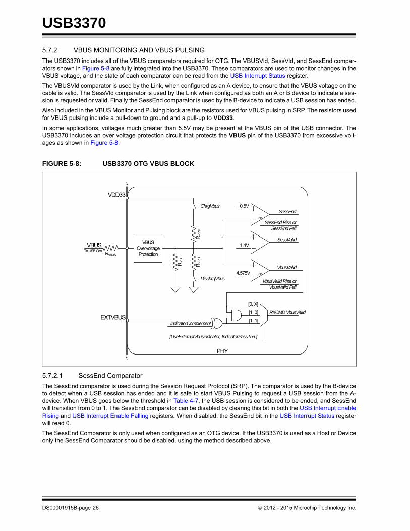
5.7.2 VBUS MONITORING AND VBUS PULSING
The USB3370 includes all of the VBUS comparators required for OTG. The VBUSVld, SessVld, and SessEnd compar-ators shown in Figure 5-8 are fully integrated into the USB3370. These comparators are used to monitor changes in theVBUS voltage, and the state of each comparator can be read from the USB Interrupt Status register.
The VBUSVld comparator is used by the Link, when configured as an A device, to ensure that the VBUS voltage on thecable is valid. The SessVld comparator is used by the Link when configured as both an A or B device to indicate a ses-sion is requested or valid. Finally the SessEnd comparator is used by the B-device to indicate a USB session has ended.
Also included in the VBUS Monitor and Pulsing block are the resistors used for VBUS pulsing in SRP. The resistors usedfor VBUS pulsing include a pull-down to ground and a pull-up to VDD33.
In some applications, voltages much greater than 5.5V may be present at the VBUS pin of the USB connector. TheUSB3370 includes an over voltage protection circuit that protects the VBUS pin of the USB3370 from excessive volt-ages as shown in Figure 5-8.
5.7.2.1 SessEnd Comparator
The SessEnd comparator is used during the Session Request Protocol (SRP). The comparator is used by the B-deviceto detect when a USB session has ended and it is safe to start VBUS Pulsing to request a USB session from the A-device. When VBUS goes below the threshold in Table 4-7, the USB session is considered to be ended, and SessEndwill transition from 0 to 1. The SessEnd comparator can be disabled by clearing this bit in both the USB Interrupt EnableRising and USB Interrupt Enable Falling registers. When disabled, the SessEnd bit in the USB Interrupt Status registerwill read 0.
The SessEnd Comparator is only used when configured as an OTG device. If the USB3370 is used as a Host or Deviceonly the SessEnd Comparator should be disabled, using the method described above.
FIGURE 5-8: USB3370 OTG VBUS BLOCK
RV
PD
VbusValid
SessValid
SessEnd
DischrgVbus
0.5V
1.4V
4.575V
VBUS
~~
~~
VDD33
PHY
To USB Con.
SessEnd Rise or SessEnd Fall
VbusValid Rise or VbusValid Fall
RXCMD VbusValid
IndicatorComplement
[UseExternalVbusindicator, IndicatorPassThru]
[0, X]
[1, 0]
[1, 1]
RV
B
RV
PU
ChrgVbus
VBUS Overvoltage ProtectionRVBUS
en
en
EXTVBUS
DS00001915B-page 26 2012 - 2015 Microchip Technology Inc.

USB3370
5.7.3 SESSVLD COMPARATOR
The SessVld comparator is used when the PHY is configured as both an A and B device. When configured as an Adevice, the SessVld is used to detect Session Request protocol (SRP). When configured as a B device, SessVld is usedto detect the presence of VBUS. The SessVld comparator output can also be read from the USB Interrupt Status regis-ter. The SessVld comparator will also generate an RX CMD, as detailed in Section 6.3.1, anytime the comparatorchanges state. The SessVld interrupts can be disabled by clearing this bit in both the USB Interrupt Enable Rising andUSB Interrupt Enable Falling registers. When the interrupts are disabled, the SessVld comparator is still operational andwill generate RX CMD’s. The SessVld comparator trip point is detailed in Table 4-8.
5.7.3.1 VbusVld Comparator
The VbusVld comparator is only used when the USB3370 is configured as a host that can supply less than 100mAVBUS current. In the USB protocol, the A-device supplies the VBUS voltage and is responsible to ensure it remainswithin a specified voltage range. The VbusVld comparator can be disabled by clearing this bit in both the USB InterruptEnable Rising and USB Interrupt Enable Falling registers. When disabled, bit 1 of the USB Interrupt Status register willreturn a 0. The VbusVld comparator threshold values are detailed in Table 4-8.
If the USB3370 is used as a Device only the VbusValid Comparator should be disabled, using the method describedabove.
The USB3370 includes the external VbusVld indicator logic as detailed in the ULPI Specification. The external VbusVldindicator is tied to a logic one. The decoding of this logic is shown in Table 5-4 below. By default this logic is disabled.
Note 5-4 A peripheral should not use VbusVld to begin operation. The peripheral should use SessVld to detectthe presence of VBUS on the USB connector. VbusVld should only be used for USB Host and OTGA-device applications.
5.7.3.2 VBUS Pulsing with Pull-up and Pull-down Resistors
In addition to the internal VBUS comparators, the USB3370 also includes the integrated VBUS pull-up and pull-downresistors used for VBUS Pulsing during OTG Session Request Protocol. To discharge the VBUS voltage so that a Ses-sion Request can begin, the USB3370 provides a pull-down resistor from VBUS to GND. This resistor is controlled bythe DischargeVbus bit 3 of the OTG Control register. The pull-up resistor is connected between VBUS and VDD33. Thisresistor is used to pull VBUS above 2.1 volts so that the A-Device knows that a USB session has been requested. Thestate of the pull-up resistor is controlled by the bit 4 ChargeVbus of the OTG Control register. The Pull-Up and Pull-Downresistor values are detailed in Table 4-8.
The internal VBUS Pull-up and Pull-down resistors are designed to include the RVBUS external resistor in series. Thisexternal resistor is used by the VBUS Over voltage protection described below.
Note: The OTG Supplement specifies a voltage range for A-Device Session Valid and B-Device Session Validcomparator. The USB3370 PHY combines the two comparators into one and uses the narrower thresholdrange.
TABLE 5-4: EXTERNAL VBUS INDICATOR LOGIC
Typical Application
Use External VBUS Indicator
Indicator Pass Thru
Indicator Complement
RXCMD VBUS ValidEncoding Source
OTG Device 0 X X Internal VbusVld comparator (Default)
1 1 0 Fixed 1
1 1 1 Fixed 0
1 0 0 Internal VbusVld comparator.
1 0 1 Fixed 0
Standard Host 1 1 0 Fixed 1
1 1 1 Fixed 0
Standard Peripheral
0 X X Internal VbusVld comparator. This information should not be used by the Link. (Note 5-4)
2012 - 2015 Microchip Technology Inc. DS00001915B-page 27
USB3370
5.7.3.3 VBUS Input Impedance
The OTG Supplement requires an A-Device that supports Session Request Protocol to have a VBUS input impedanceless than 100kΩ and greater the 40kΩ to ground. The USB3370 provides a 75kΩ resistance to ground, RVB. The RVBresistor tolerance is detailed in Table 4-8.
5.7.3.4 VBUS Over Voltage Protection (OVP)
The USB3370 provides an integrated over voltage protection circuit to protect the VBUS pin from excessive voltagesthat may be present at the USB connector. The over voltage protection circuit works with an external resistor (RVBUS)by drawing current across the resistor to reduce the voltage at the VBUS pin.
When voltage at the VBUS pin exceeds 5.5V, the Over voltage Protection block will sink current to ground until VBUSis below 5.5V. The current drops the excess voltage across RVBUS and protects the USB3370 VBUS pin. The requiredRVBUS value is dependent on the operating mode of the USB3370 as shown in Table 5-5.
The Over voltage Protection circuit is designed to protect the USB3370 from continuous voltages up to 30V on theRVBUS resistor.
The RVBUS resistor must be sized to handle the power dissipated across the resistor. The resistor power can be foundusing the equation below:
For example, protecting a peripheral or device only application to 15V would require a 20kΩ RVBUS resistor with a powerrating of 0.05W. To protect an OTG product to 15V would require a 1kΩ RVBUS resistor with a power rating of 0.1W.
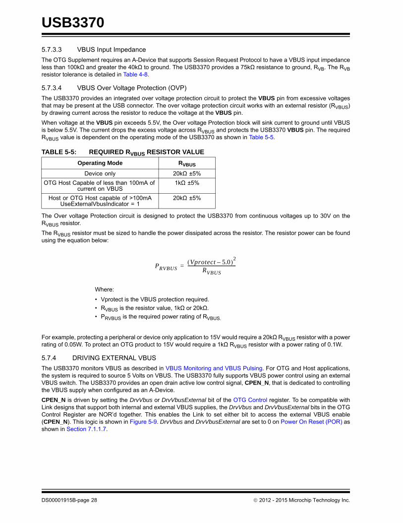
5.7.4 DRIVING EXTERNAL VBUS
The USB3370 monitors VBUS as described in VBUS Monitoring and VBUS Pulsing. For OTG and Host applications,the system is required to source 5 Volts on VBUS. The USB3370 fully supports VBUS power control using an externalVBUS switch. The USB3370 provides an open drain active low control signal, CPEN_N, that is dedicated to controllingthe VBUS supply when configured as an A-Device.
CPEN_N is driven by setting the DrvVbus or DrvVbusExternal bit of the OTG Control register. To be compatible withLink designs that support both internal and external VBUS supplies, the DrvVbus and DrvVbusExternal bits in the OTGControl Register are NOR’d together. This enables the Link to set either bit to access the external VBUS enable(CPEN_N). This logic is shown in Figure 5-9. DrvVbus and DrvVbusExternal are set to 0 on Power On Reset (POR) asshown in Section 7.1.1.7.
TABLE 5-5: REQUIRED RVBUS RESISTOR VALUE
Operating Mode RVBUS
Device only 20kΩ ±5%
OTG Host Capable of less than 100mA of current on VBUS
1kΩ ±5%
Host or OTG Host capable of >100mAUseExternalVbusIndicator = 1
20kΩ ±5%
PRVBUSVprotect 5.0–( )2
RVBUS--------------------------------------------=
Where:
• Vprotect is the VBUS protection required.
• RVBUS is the resistor value, 1kΩ or 20kΩ.
• PRVBUS is the required power rating of RVBUS.
DS00001915B-page 28 2012 - 2015 Microchip Technology Inc.
USB3370
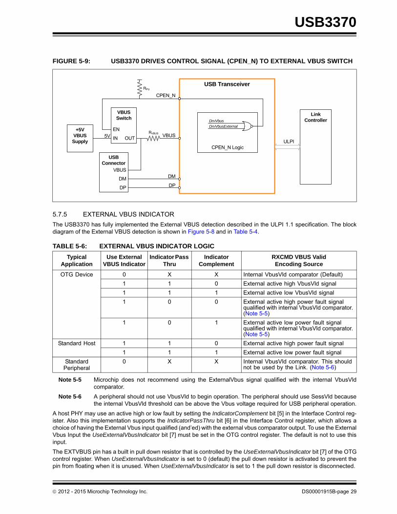
5.7.5 EXTERNAL VBUS INDICATOR
The USB3370 has fully implemented the External VBUS detection described in the ULPI 1.1 specification. The blockdiagram of the External VBUS detection is shown in Figure 5-8 and in Table 5-4.
Note 5-5 Microchip does not recommend using the ExternalVbus signal qualified with the internal VbusVldcomparator.
Note 5-6 A peripheral should not use VbusVld to begin operation. The peripheral should use SessVld becausethe internal VbusVld threshold can be above the Vbus voltage required for USB peripheral operation.
A host PHY may use an active high or low fault by setting the IndicatorComplement bit [5] in the Interface Control reg-ister. Also this implementation supports the IndicatorPassThru bit [6] in the Interface Control register, which allows achoice of having the External Vbus input qualified (and’ed) with the external vbus comparator output. To use the ExternalVbus Input the UseExternalVbusIndicator bit [7] must be set in the OTG control register. The default is not to use thisinput.
The EXTVBUS pin has a built in pull down resistor that is controlled by the UseExternalVbusIndicator bit [7] of the OTGcontrol register. When UseExternalVbusIndicator is set to 0 (default) the pull down resistor is activated to prevent thepin from floating when it is unused. When UseExternalVbusIndicator is set to 1 the pull down resistor is disconnected.
FIGURE 5-9: USB3370 DRIVES CONTROL SIGNAL (CPEN_N) TO EXTERNAL VBUS SWITCH
TABLE 5-6: EXTERNAL VBUS INDICATOR LOGIC
Typical Application
Use External VBUS Indicator
Indicator Pass Thru
Indicator Complement
RXCMD VBUS ValidEncoding Source
OTG Device 0 X X Internal VbusVld comparator (Default)
1 1 0 External active high VbusVld signal
1 1 1 External active low VbusVld signal
1 0 0 External active high power fault signal qualified with internal VbusVld comparator. (Note 5-5)
1 0 1 External active low power fault signal qualified with internal VbusVld comparator. (Note 5-5)
Standard Host 1 1 0 External active high power fault signal
1 1 1 External active low power fault signal
Standard Peripheral
0 X X Internal VbusVld comparator. This should not be used by the Link. (Note 5-6)
VBUS Switch
OUT
EN
IN5V
USB Transceiver
VBUS
USB Connector
DM
DP
VBUS
RVBUS
CPEN_N
Link Controller
CPEN_N Logic
DrvVbusExternalDrvVbus
DM
DP
ULPI
+5VVBUS Supply
RPU
2012 - 2015 Microchip Technology Inc. DS00001915B-page 29
USB3370
5.8 USB UART Support
The USB3370 provides support for the USB UART interface as detailed in the ULPI specification and the former CEA-936A specification. The USB3370 can be placed in UART Mode using the method described in Section 6.7, and theregulator output will automatically switch to the value configured by the UART RegOutput bits in the USB IO & PowerManagement register. While in UART mode, the Linestate signals cannot be monitored on the DATA[0] and DATA[1]pins.
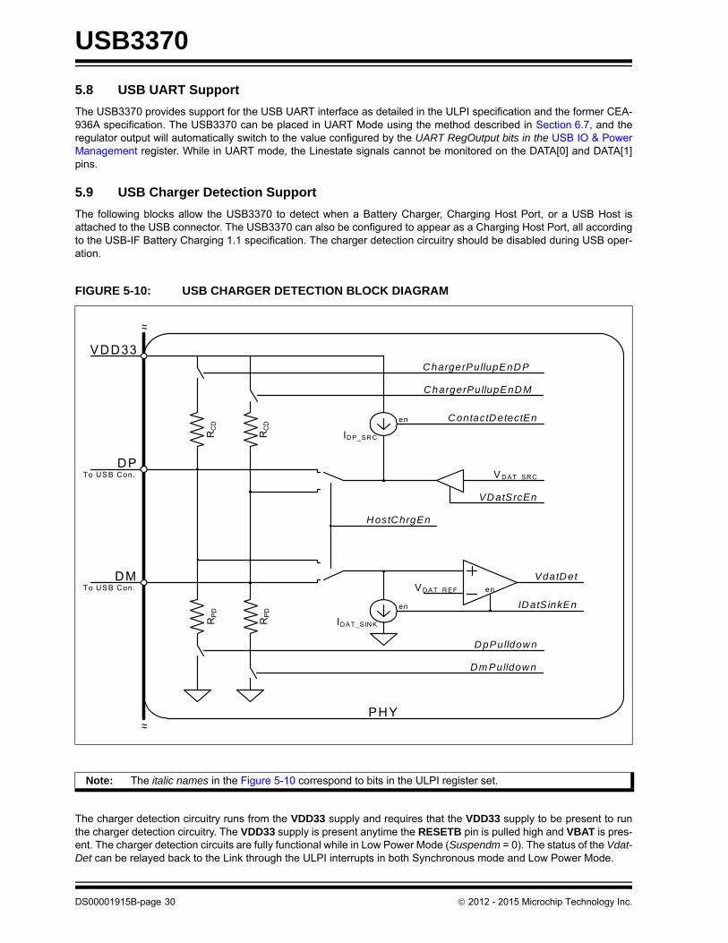
5.9 USB Charger Detection Support
The following blocks allow the USB3370 to detect when a Battery Charger, Charging Host Port, or a USB Host isattached to the USB connector. The USB3370 can also be configured to appear as a Charging Host Port, all accordingto the USB-IF Battery Charging 1.1 specification. The charger detection circuitry should be disabled during USB oper-ation.
The charger detection circuitry runs from the VDD33 supply and requires that the VDD33 supply to be present to runthe charger detection circuitry. The VDD33 supply is present anytime the RESETB pin is pulled high and VBAT is pres-ent. The charger detection circuits are fully functional while in Low Power Mode (Suspendm = 0). The status of the Vdat-Det can be relayed back to the Link through the ULPI interrupts in both Synchronous mode and Low Power Mode.
FIGURE 5-10: USB CHARGER DETECTION BLOCK DIAGRAM
Note: The italic names in the Figure 5-10 correspond to bits in the ULPI register set.
VDAT_R EF
DP
~~
~~
VDD33
PHY
To USB Con.
RC
D
ChargerPullupEnDP
en
DMTo USB Con.
RC
D
ChargerPullupEnDM
IDatSinkEn
HostChrgEn
VdatDet
VDatSrcEn
IDAT_SIN K
en
V D AT_SR C
ContactDetectEn
IDP_SR C
en
DpPulldown
Dm Pulldown
RP
D
RP
D
DS00001915B-page 30 2012 - 2015 Microchip Technology Inc.
USB3370
5.9.1 ACTIVE ANALOG CHARGER DETECTION (USB-IF BATTERY CHARGING 1.1)
The USB3370 includes the active analog charger detection specified in the USB-IF Battery Charging Specification. Theadditional analog circuitry will allow the USB3370 to:
1. Detect a Dedicated Charging Port (DCP) with the DP and DM pins shorted together.
2. Detect a Standard Downstream Port (SDP) which has no battery charging circuitry.
3. Detect a Charging Downstream Port (CDP) which actively supplies voltage to the DM pin when connected to aUSB-IF BC 1.1 compatible device.
4. Behave as a Charging Downstream Port by enabling the voltage source on the DM pin.
The charger detection circuitry is shown in Figure 5-10.
The VdatDet output is qualified with the Linestate[1:0] value. If the Linestate is not equal to 00 the VdatDet signal willnot assert.
The proper detection process flows through different modes of detection and uses the linestate and VdatDet signalsvalues to determine the connection. Table 5-7 describes the bit values that need to be set to enter each mode.
5.9.1.1 Example Charger Detection Flow - Dedicated Charging Port
The USB-IF Battery Charging 1.1 specification describes in detail the flow for each charger type, but below is an exam-ple of the flow used to detect a Dedicated Charger (DCP).
1. Device detects VBUS voltage is present from RXCMD, (SESS_VLD is 1)
2. Device enters the Device Connect Detect mode.
- If the linestate still equals 10 after a specified timeout, the charger is an unknown charger and there will be no attempted USB enumeration.
- If the linestate equals 00 or 11, the device will go to the next mode:
3. Device enters Device Charger Detection mode.
- If the VdatDet bit is 0 then the host is a Standard Downstream Port (SDP) and the device will draw the stan-dard 500mA of current and enter the Device USB Operation mode.
- If the VdatDet bit is 1 then the host is a charger that can supply at least 1.5A of current, the device will go to the next mode.
4. Device enters Device Enhanced Charger Detection mode.
- If the VdatDet bit is 0 then the device is connected to a Charging Downstream Port (CDP) and the device will enter the Device USB Operation mode.
- If the VdatDet bit is 1 then the device is connected to a Dedicated Charging Port (DCP) and the device will not try to enumerate.
5. The charger detection is complete.
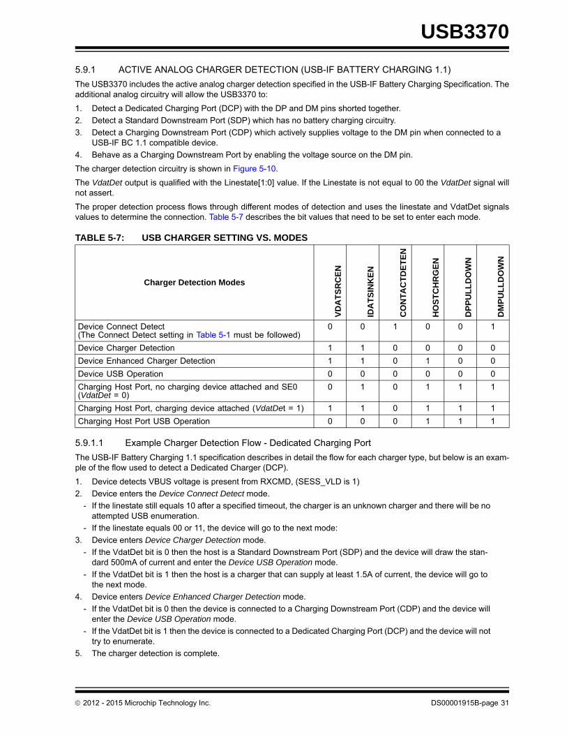
TABLE 5-7: USB CHARGER SETTING VS. MODES
Charger Detection Modes
VD
AT
SR
CE
N
IDA
TS
INK
EN
CO
NT
AC
TD
ET
EN
HO
ST
CH
RG
EN
DP
PU
LL
DO
WN
DM
PU
LL
DO
WN
Device Connect Detect(The Connect Detect setting in Table 5-1 must be followed)
0 0 1 0 0 1
Device Charger Detection 1 1 0 0 0 0
Device Enhanced Charger Detection 1 1 0 1 0 0
Device USB Operation 0 0 0 0 0 0
Charging Host Port, no charging device attached and SE0 (VdatDet = 0)
0 1 0 1 1 1
Charging Host Port, charging device attached (VdatDet = 1) 1 1 0 1 1 1
Charging Host Port USB Operation 0 0 0 1 1 1
2012 - 2015 Microchip Technology Inc. DS00001915B-page 31
USB3370
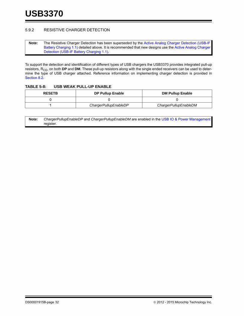
5.9.2 RESISTIVE CHARGER DETECTION
To support the detection and identification of different types of USB chargers the USB3370 provides integrated pull-upresistors, RCD, on both DP and DM. These pull-up resistors along with the single ended receivers can be used to deter-mine the type of USB charger attached. Reference information on implementing charger detection is provided inSection 8.2.
Note: The Resistive Charger Detection has been superseded by the Active Analog Charger Detection (USB-IFBattery Charging 1.1) detailed above. It is recommended that new designs use the Active Analog ChargerDetection (USB-IF Battery Charging 1.1).
TABLE 5-8: USB WEAK PULL-UP ENABLE
RESETB DP Pullup Enable DM Pullup Enable
0 0 0
1 ChargerPullupEnableDP ChargerPullupEnableDM
Note: ChargerPullupEnableDP and ChargerPullupEnableDM are enabled in the USB IO & Power Managementregister.
DS00001915B-page 32 2012 - 2015 Microchip Technology Inc.
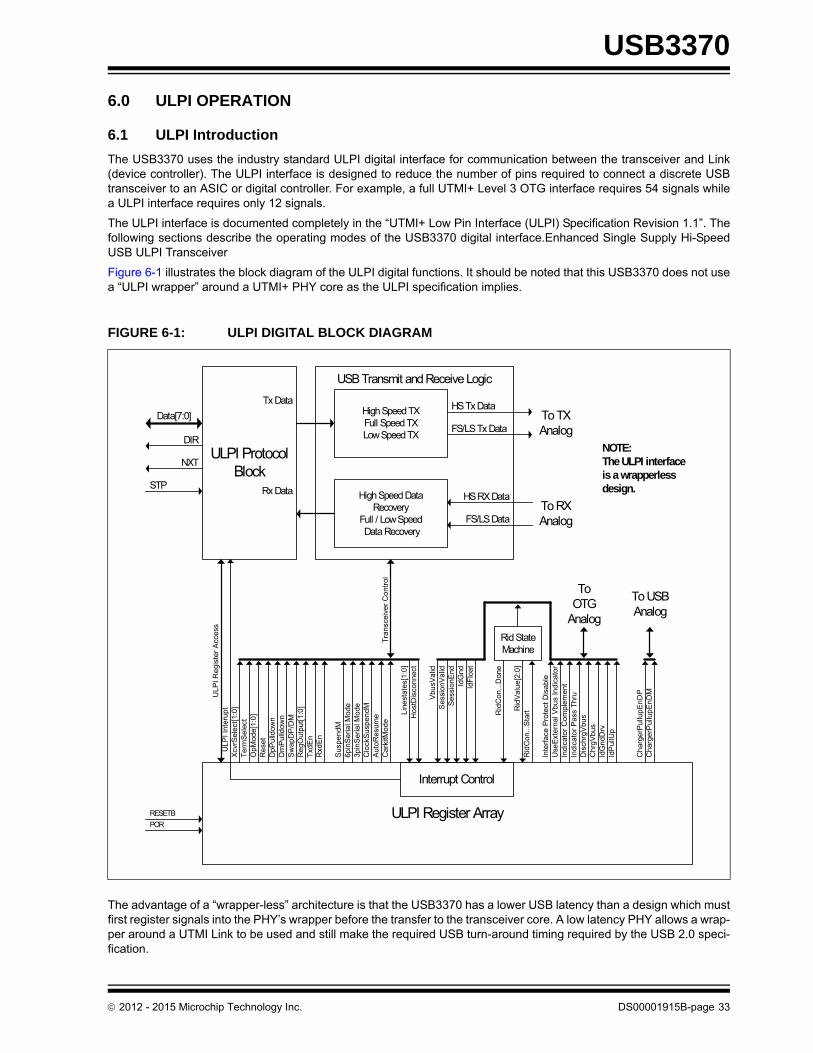
USB3370
6.0 ULPI OPERATION
6.1 ULPI Introduction
The USB3370 uses the industry standard ULPI digital interface for communication between the transceiver and Link(device controller). The ULPI interface is designed to reduce the number of pins required to connect a discrete USBtransceiver to an ASIC or digital controller. For example, a full UTMI+ Level 3 OTG interface requires 54 signals whilea ULPI interface requires only 12 signals.
The ULPI interface is documented completely in the “UTMI+ Low Pin Interface (ULPI) Specification Revision 1.1”. Thefollowing sections describe the operating modes of the USB3370 digital interface.Enhanced Single Supply Hi-SpeedUSB ULPI Transceiver
Figure 6-1 illustrates the block diagram of the ULPI digital functions. It should be noted that this USB3370 does not usea “ULPI wrapper” around a UTMI+ PHY core as the ULPI specification implies.
The advantage of a “wrapper-less” architecture is that the USB3370 has a lower USB latency than a design which mustfirst register signals into the PHY’s wrapper before the transfer to the transceiver core. A low latency PHY allows a wrap-per around a UTMI Link to be used and still make the required USB turn-around timing required by the USB 2.0 speci-fication.
FIGURE 6-1: ULPI DIGITAL BLOCK DIAGRAM
NOTE:The ULPI interface is a wrapperless design.
PORULPI Register Array
Interrupt Control
6pin
Se
rial M
ode
Xcv
rSel
ect
[1:0
]T
erm
Sel
ect
OpM
ode[
1:0
]R
ese
t
Sus
pen
dM
3pin
Se
rial M
ode
Clo
ckS
usp
endM
Aut
oRes
um
e
Dis
chrg
Vb
usC
hrg
Vb
usId
Gn
dDrv
Dp
Pu
lldow
nD
mP
ulld
own
Sw
apD
P/D
M
Ca
rkitM
ode
Re
gOut
put
[1:0
]
Ch
arge
rPul
lup
En
DP
Ch
arge
rPul
lup
En
DM
Txd
En
Rxd
En
Ind
icat
or
Co
mp
lem
ent
Ind
icat
or
Pas
s T
hru
Use
Ext
ern
al V
bus
Indi
cato
r
IdP
ullU
p
Line
stat
es[1
:0]
Ho
stD
isco
nne
ct
Inte
rfac
e P
rote
ct D
isa
ble
Vbu
sVa
lidS
essi
onV
alid
Se
ssio
nE
ndId
Gnd
IdF
loa
t
Rid
Co
n...S
tartR
idV
alu
e[2
:0]
Rid
Con
...D
one
Data[7:0] High Speed TXFull Speed TXLow Speed TX
High Speed DataRecovery
Full / Low Speed Data Recovery
ULPI Protocol Block
HS Tx Data
FS/LS Tx Data
HS RX Data
FS/LS Data
DIR
NXT
STP
Tx Data
Rx Data
USB Transmit and Receive Logic
ULP
I Re
gist
er A
cces
s
RESETB
UL
PI
Inte
rup
t
Rid State Machine
To RX Analog
To TX Analog
Tra
nsc
eive
r C
ont
rol
To OTG
Analog
To USBAnalog
2012 - 2015 Microchip Technology Inc. DS00001915B-page 33
USB3370
RxEndDelay maximum allowed by the UTMI+/ULPI for 8-bit data is 63 Hi-Speed clocks. USB3370 uses a low latencyHi-Speed receiver path to lower the RxEndDelay to 43 Hi-Speed clocks. This low latency design gives the Link morecycles to make decisions and reduces the Link complexity. This is the result of the “wrapper less” architecture of theUSB3370. This low RxEndDelay should allow legacy UTMI Links to use a “wrapper” to convert the UTMI+ interface toa ULPI interface.
In Figure 6-1, a single ULPI Protocol Block decodes the ULPI 8-bit bi-directional bus when the Link addresses the PHY.The Link must use the DIR output to determine direction of the ULPI data bus. The USB3370 is the “bus arbitrator”. TheULPI Protocol Block will route data/commands to the transmitter or the ULPI register array.
6.1.1 ULPI INTERFACE SIGNALS
The UTMI+ Low Pin Interface (ULPI) uses a 12-pin interface to connect a USB Transceiver to an external Link. Thereduction of external pins, relative to UTMI+, is accomplished implementing the relatively static configuration pins (i.e.xcvrselect[1:0], termselect, opmode[1:0], and DpPullDown DmPulldown) as an internal register array.
An 8-bit bi-directional data bus clocked at 60MHz allows the Link to access this internal register array and transfer USBpackets to and from the PHY. The remaining 3 pins function to control the data flow and arbitrate the data bus.
Direction of the 8-bit data bus is controlled by the DIR output from the PHY. Another output, NXT, is used to controldata flow into and out of the device. Finally, STP, which is in input to the PHY, terminates transfers and is used to startup and resume from Low Power Mode.
The ULPI Interface signals are described below in Table 6-1.
USB3370 implements a Single Data Rate (SDR) ULPI interface with all data transfers happening on the rising edge ofthe 60MHz ULPI Clock while operating in Synchronous Mode. The direction of the data bus is determined by the stateof DIR. When DIR is high, the PHY is driving DATA[7:0]. When DIR is low, the Link is driving DATA[7:0].
Each time DIR changes, a “turn-around” cycle occurs where neither the Link nor PHY drive the data bus for one clockcycle. During the “turn-around“cycle, the state of DATA[7:0] is unknown and the PHY will not read the data bus.
Because USB uses a bit-stuffing encoding, some means of allowing the PHY to throttle the USB transmit data is needed.The ULPI signal NXT is used to request the next byte to be placed on the data bus by the Link.
The ULPI interface supports the two basic modes of operation: Synchronous Mode and Asynchronous Mode. Asynchro-nous Mode includes Low Power Mode, the Serial Modes, and Carkit Mode. In Synchronous Mode, all signals changesynchronously with the 60MHz ULPI clock. In asynchronous modes the clock is off and the ULPI bus is redefined tobring out the signals required for that particular mode of operations. The description of synchronous Mode is describedin the following sections while the descriptions of the asynchronous modes are described in Section 6.5, Section 6.6,and Section 6.7.
TABLE 6-1: ULPI INTERFACE SIGNALS
Signal Direction Description
CLK I/O 60MHz ULPI clock. All ULPI signals are driven synchronous to the rising edge of this clock. This clock can be either driven by the PHY or the Link as described in Section 5.5.1
DATA[7:0] I/O 8-bit bi-directional data bus. Bus ownership is determined by DIR. The Link and PHY initiate data transfers by driving a non-zero pattern onto the data bus. ULPI defines interface timing for a single-edge data transfers with respect to rising edge of the ULPI clock.
DIR OUT Controls the direction of the data bus. When the PHY has data to transfer to the Link, it drives DIR high to take ownership of the bus. When the PHY has no data to transfer it drives DIR low and monitors the bus for commands from the Link. The PHY will pull DIR high whenever the interface cannot accept data from the Link, such as during PLL start-up.
STP IN The Link asserts STP for one clock cycle to stop the data stream currently on the bus. If the Link is sending data to the PHY, STP indicates the last byte of data was on the bus in the previous cycle.
NXT OUT The PHY asserts NXT to throttle the data. When the Link is sending data to the PHY, NXT indicates when the current byte has been accepted by the PHY. The Link places the next byte on the data bus in the following clock cycle.
DS00001915B-page 34 2012 - 2015 Microchip Technology Inc.

USB3370
6.1.2 ULPI INTERFACE TIMING IN SYNCHRONOUS MODE
The control and data timing relationships are given in Figure 6-2 and Table 4-3. All timing is relative to the rising clockedge of the 60MHz ULPI Clock.
6.2 ULPI Register Access
The following section details the steps required to access registers through the ULPI interface. At any time DIR is lowthe Link may access the ULPI registers set using the Transmit Command byte. The ULPI registers retain their contentswhen the PHY is in Low Power Mode, Full Speed/Low Speed Serial Mode, or Carkit Mode.
6.2.1 TRANSMIT COMMAND BYTE (TX CMD)
A command from the Link begins a ULPI transfer from the Link to the USB3370. Before reading a ULPI register, the Linkmust wait until DIR is low, and then send a Transmit Command Byte (TX CMD) byte. The TX CMD byte informs theUSB3370 of the type of data being sent. The TX CMD is followed by a data transfer to or from the USB3370. Table 6-2gives the TX command byte (TX CMD) encoding for the USB3370. The upper two bits of the TX CMD instruct the PHYas to what type of packet the Link is transmitting.
FIGURE 6-2: ULPI SINGLE DATA RATE TIMING DIAGRAM IN SYNCHRONOUS MODE
TABLE 6-2: ULPI TX CMD BYTE ENCODING
Command Name CMD Bits[7:6] CMD Bits[5:0] Command Description
Idle 00b 000000b ULPI Idle
Transmit 01b 000000b USB Transmit Packet with No Packet Identifier (NOPID)
00XXXXb USB Transmit Packet Identifier (PID) where DATA[3:0] is equal to the 4-bit PID. P3P2P1P0 where P3 is the MSB.
Register Write 10b XXXXXXb Immediate Register Write Command where: DATA[5:0] = 6-bit register address
101111b Extended Register Write Command where the 8-bit register address is available on the next cycle.
60MHz ULPI -CLK
Control In - STP
Data In - DATA[7:0]
Control Out - DIR, NXT
Data Out - DATA[7:0]
TSC
TSD
THC
THD
TDC TDC
TDD
2012 - 2015 Microchip Technology Inc. DS00001915B-page 35
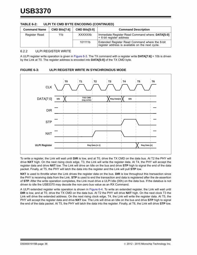
USB3370
6.2.2 ULPI REGISTER WRITE
A ULPI register write operation is given in Figure 6-3. The TX command with a register write DATA[7:6] = 10b is drivenby the Link at T0. The register address is encoded into DATA[5:0] of the TX CMD byte.
To write a register, the Link will wait until DIR is low, and at T0, drive the TX CMD on the data bus. At T2 the PHY willdrive NXT high. On the next rising clock edge, T3, the Link will write the register data. At T4, the PHY will accept theregister data and drive NXT low. The Link will drive an Idle on the bus and drive STP high to signal the end of the datapacket. Finally, at T5, the PHY will latch the data into the register and the Link will pull STP low.
NXT is used to throttle when the Link drives the register data on the bus. DIR is low throughout this transaction sincethe PHY is receiving data from the Link. STP is used to end the transaction and data is registered after the de-assertionof STP. After the write operation completes, the Link must drive a ULPI Idle (00h) on the data bus. If the databus is notdriven to idle the USB3370 may decode the non-zero bus value as an RX Command.
A ULPI extended register write operation is shown in Figure 6-4. To write an extended register, the Link will wait untilDIR is low, and at T0, drive the TX CMD on the data bus. At T2 the PHY will drive NXT high. On the next clock T3 theLink will drive the extended address. On the next rising clock edge, T4, the Link will write the register data. At T5, thePHY will accept the register data and drive NXT low. The Link will drive an Idle on the bus and drive STP high to signalthe end of the data packet. At T5, the PHY will latch the data into the register. Finally, at T6, the Link will drive STP low.
Register Read 11b XXXXXXb Immediate Register Read Command where: DATA[5:0] = 6-bit register address
101111b Extended Register Read Command where the 8-bit register address is available on the next cycle.
FIGURE 6-3: ULPI REGISTER WRITE IN SYNCHRONOUS MODE
TABLE 6-2: ULPI TX CMD BYTE ENCODING (CONTINUED)
Command Name CMD Bits[7:6] CMD Bits[5:0] Command Description
DIR
CLK
DATA[7:0]
STP
NXT
TXD CMD (reg write) Idle Reg Data[n] Idle
ULPI Register Reg Data [n-1] Reg Data [n]
T0 T1 T2 T3 T5T4 T6
DS00001915B-page 36 2012 - 2015 Microchip Technology Inc.
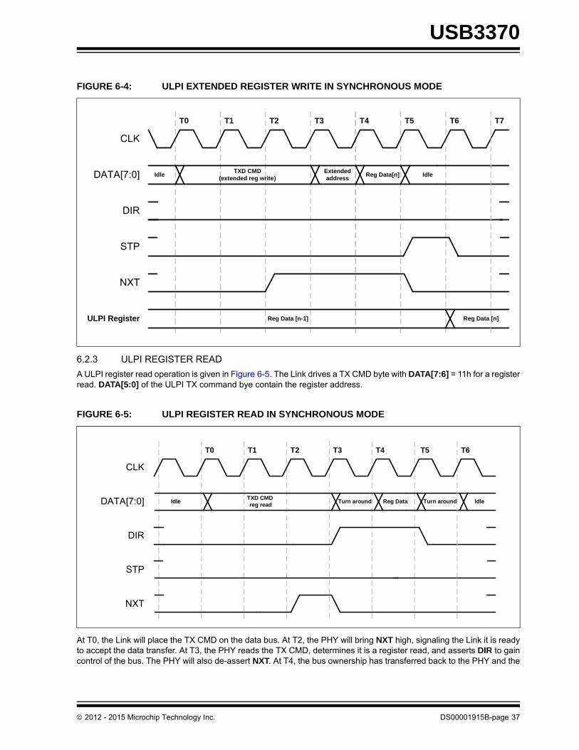
USB3370
6.2.3 ULPI REGISTER READ
A ULPI register read operation is given in Figure 6-5. The Link drives a TX CMD byte with DATA[7:6] = 11h for a registerread. DATA[5:0] of the ULPI TX command bye contain the register address.
At T0, the Link will place the TX CMD on the data bus. At T2, the PHY will bring NXT high, signaling the Link it is readyto accept the data transfer. At T3, the PHY reads the TX CMD, determines it is a register read, and asserts DIR to gaincontrol of the bus. The PHY will also de-assert NXT. At T4, the bus ownership has transferred back to the PHY and the
FIGURE 6-4: ULPI EXTENDED REGISTER WRITE IN SYNCHRONOUS MODE
FIGURE 6-5: ULPI REGISTER READ IN SYNCHRONOUS MODE
DIR
CLK
DATA[7:0]
STP
NXT
TXD CMD (extended reg write) Idle Reg Data[n] Idle
ULPI Register Reg Data [n-1] Reg Data [n]
T0 T1 T2 T3 T5T4 T6
Extendedaddress
T7
DIR
CLK
DATA[7:0]
STP
NXT
TXD CMD reg read Idle
T0
Reg DataTurn around Turn around
T1 T2 T3 T4 T5 T6
Idle
2012 - 2015 Microchip Technology Inc. DS00001915B-page 37

USB3370
PHY drives the requested register onto the data bus. At T5, the Link will read the data bus and the PHY will drop DIRlow returning control of the bus back to the Link. After the turn around cycle, the Link must drive a ULPI Idle commandat T6.
A ULPI extended register read operation is shown in Figure 6-6.To read an extended register, the Link writes the TXCMD with the address set to 2Fh. At T2, the PHY will assert NXT, signaling the Link it is ready to accept the extendedaddress. At T3, the Link places the extended register address on the bus. At T4, the PHY reads the extended address,and asserts DIR to gain control of the bus. The PHY will also de-assert NXT. At T5, the bus ownership has transferredback to the PHY and the PHY drives the requested register onto the data bus. At T6, the Link will read the data bus andthe PHY will de-assert DIR returning control of the bus back to the Link. After the turn around cycle, the Link must drivea ULPI Idle command at T6.
6.3 USB3370 Receiver
The following section describes how the USB3370 uses the ULPI interface to receive USB signaling and transfer statusinformation to the Link. This information is communicated to the Link using RX Commands to relay bus status andreceived USB packets.
6.3.1 ULPI RECEIVE COMMAND (RX CMD)
The ULPI Link needs information which was provided by the following pins in a UTMI implementation: linestate[1:0],rxactive, rxvalid, rxerror, and VbusValid. When implementing the OTG functions, the VBUS and ID pin states must alsobe transferred to the Link. ULPI defines a Receive Command Byte (RXCMD) that contains this information.
An RXCMD can be sent a any time the bus is idle. The RXCMD is initiated when the USB3370 asserts DIR to take con-trol of the bus. The timing of RXCMD is shown in the figure below. The USB3370 can send single or back to backRXCMD’s as required. The Encoding of the RXCMD byte is given in the Table 6-3.
FIGURE 6-6: ULPI EXTENDED REGISTER READ IN SYNCHRONOUS MODE
DIR
CLK
DATA[7:0]
STP
NXT
TXD CMDextended reg read Idle
T0
Reg DataTurn around Turn around
T1 T2 T3 T4 T5 T6
IdleExtendedaddress
T7
DS00001915B-page 38 2012 - 2015 Microchip Technology Inc.
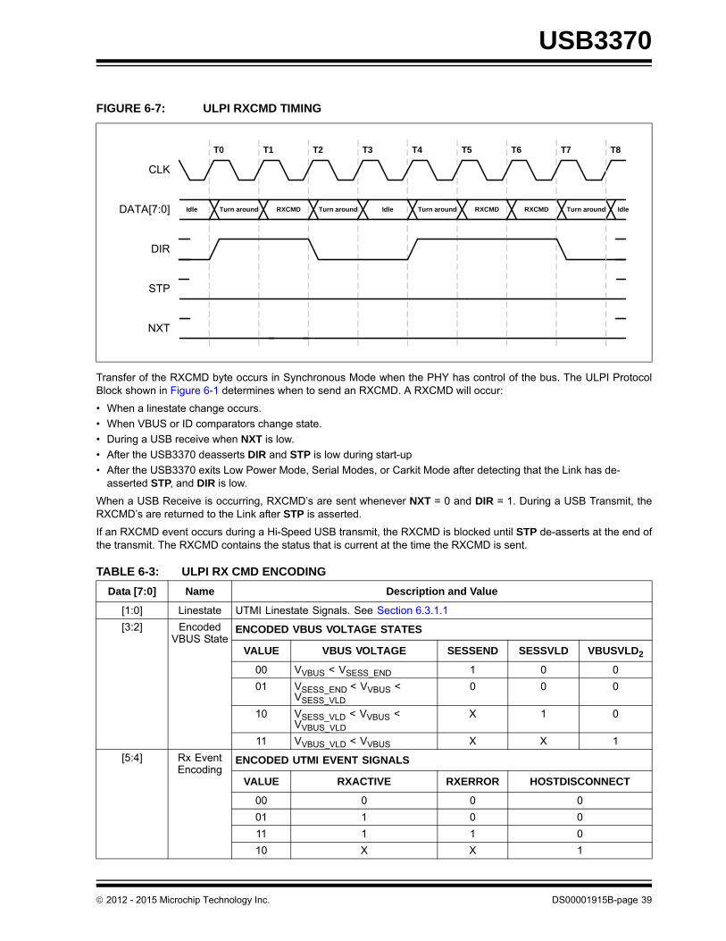
USB3370
Transfer of the RXCMD byte occurs in Synchronous Mode when the PHY has control of the bus. The ULPI ProtocolBlock shown in Figure 6-1 determines when to send an RXCMD. A RXCMD will occur:
• When a linestate change occurs.
• When VBUS or ID comparators change state.
• During a USB receive when NXT is low.
• After the USB3370 deasserts DIR and STP is low during start-up
• After the USB3370 exits Low Power Mode, Serial Modes, or Carkit Mode after detecting that the Link has de-asserted STP, and DIR is low.
When a USB Receive is occurring, RXCMD’s are sent whenever NXT = 0 and DIR = 1. During a USB Transmit, theRXCMD’s are returned to the Link after STP is asserted.
If an RXCMD event occurs during a Hi-Speed USB transmit, the RXCMD is blocked until STP de-asserts at the end ofthe transmit. The RXCMD contains the status that is current at the time the RXCMD is sent.
FIGURE 6-7: ULPI RXCMD TIMING
TABLE 6-3: ULPI RX CMD ENCODING
Data [7:0] Name Description and Value
[1:0] Linestate UTMI Linestate Signals. See Section 6.3.1.1
[3:2] Encoded VBUS State
ENCODED VBUS VOLTAGE STATES
VALUE VBUS VOLTAGE SESSEND SESSVLD VBUSVLD2
00 VVBUS < VSESS_END 1 0 0
01 VSESS_END < VVBUS < VSESS_VLD
0 0 0
10 VSESS_VLD < VVBUS < VVBUS_VLD
X 1 0
11 VVBUS_VLD < VVBUS X X 1
[5:4] Rx Event Encoding
ENCODED UTMI EVENT SIGNALS
VALUE RXACTIVE RXERROR HOSTDISCONNECT
00 0 0 0
01 1 0 0
11 1 1 0
10 X X 1
DIR
CLK
DATA[7:0]
STP
NXT
RXCMD Idle Idle
T0 T1 T2 T3 T5T4 T6
Turn around Turn around RXCMD IdleTurn around Turn aroundRXCMD
T7 T8
2012 - 2015 Microchip Technology Inc. DS00001915B-page 39
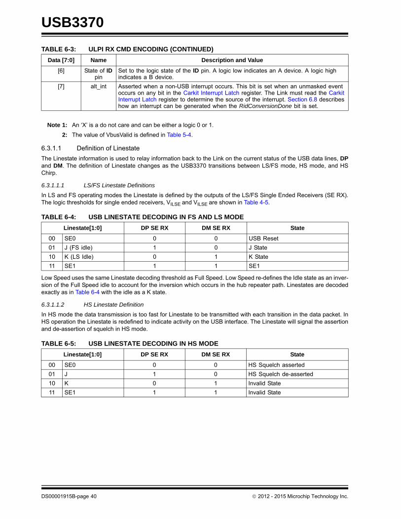
USB3370
Note 1: An ‘X’ is a do not care and can be either a logic 0 or 1.
2: The value of VbusValid is defined in Table 5-4.
6.3.1.1 Definition of Linestate
The Linestate information is used to relay information back to the Link on the current status of the USB data lines, DPand DM. The definition of Linestate changes as the USB3370 transitions between LS/FS mode, HS mode, and HSChirp.
6.3.1.1.1 LS/FS Linestate Definitions
In LS and FS operating modes the Linestate is defined by the outputs of the LS/FS Single Ended Receivers (SE RX).The logic thresholds for single ended receivers, VILSE and VILSE are shown in Table 4-5.
Low Speed uses the same Linestate decoding threshold as Full Speed. Low Speed re-defines the Idle state as an inver-sion of the Full Speed idle to account for the inversion which occurs in the hub repeater path. Linestates are decodedexactly as in Table 6-4 with the idle as a K state.
6.3.1.1.2 HS Linestate Definition
In HS mode the data transmission is too fast for Linestate to be transmitted with each transition in the data packet. InHS operation the Linestate is redefined to indicate activity on the USB interface. The Linestate will signal the assertionand de-assertion of squelch in HS mode.
[6] State of ID pin
Set to the logic state of the ID pin. A logic low indicates an A device. A logic high indicates a B device.
[7] alt_int Asserted when a non-USB interrupt occurs. This bit is set when an unmasked event occurs on any bit in the Carkit Interrupt Latch register. The Link must read the Carkit Interrupt Latch register to determine the source of the interrupt. Section 6.8 describes how an interrupt can be generated when the RidConversionDone bit is set.
TABLE 6-4: USB LINESTATE DECODING IN FS AND LS MODE
Linestate[1:0] DP SE RX DM SE RX State
00 SE0 0 0 USB Reset
01 J (FS idle) 1 0 J State
10 K (LS Idle) 0 1 K State
11 SE1 1 1 SE1
TABLE 6-5: USB LINESTATE DECODING IN HS MODE
Linestate[1:0] DP SE RX DM SE RX State
00 SE0 0 0 HS Squelch asserted
01 J 1 0 HS Squelch de-asserted
10 K 0 1 Invalid State
11 SE1 1 1 Invalid State
TABLE 6-3: ULPI RX CMD ENCODING (CONTINUED)
Data [7:0] Name Description and Value
DS00001915B-page 40 2012 - 2015 Microchip Technology Inc.
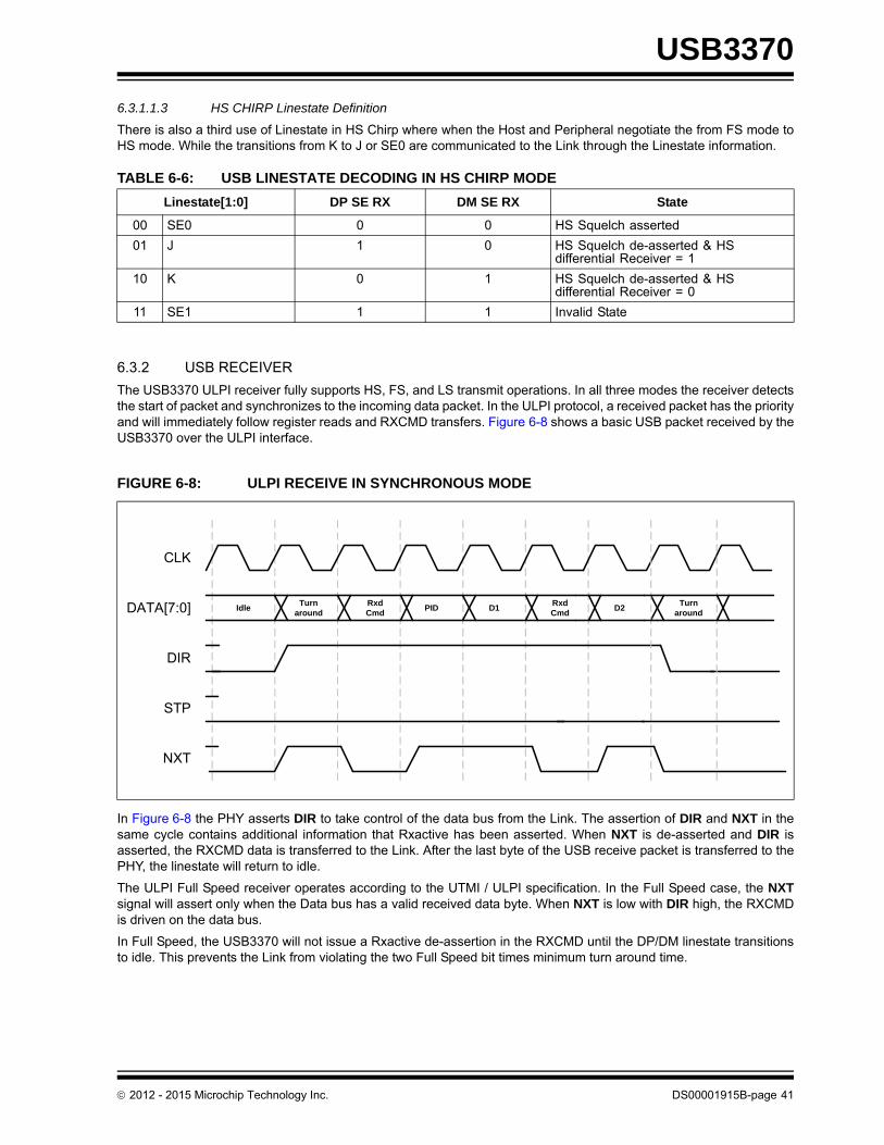
USB3370
6.3.1.1.3 HS CHIRP Linestate Definition
There is also a third use of Linestate in HS Chirp where when the Host and Peripheral negotiate the from FS mode toHS mode. While the transitions from K to J or SE0 are communicated to the Link through the Linestate information.
6.3.2 USB RECEIVER
The USB3370 ULPI receiver fully supports HS, FS, and LS transmit operations. In all three modes the receiver detectsthe start of packet and synchronizes to the incoming data packet. In the ULPI protocol, a received packet has the priorityand will immediately follow register reads and RXCMD transfers. Figure 6-8 shows a basic USB packet received by theUSB3370 over the ULPI interface.
In Figure 6-8 the PHY asserts DIR to take control of the data bus from the Link. The assertion of DIR and NXT in thesame cycle contains additional information that Rxactive has been asserted. When NXT is de-asserted and DIR isasserted, the RXCMD data is transferred to the Link. After the last byte of the USB receive packet is transferred to thePHY, the linestate will return to idle.
The ULPI Full Speed receiver operates according to the UTMI / ULPI specification. In the Full Speed case, the NXTsignal will assert only when the Data bus has a valid received data byte. When NXT is low with DIR high, the RXCMDis driven on the data bus.
In Full Speed, the USB3370 will not issue a Rxactive de-assertion in the RXCMD until the DP/DM linestate transitionsto idle. This prevents the Link from violating the two Full Speed bit times minimum turn around time.
TABLE 6-6: USB LINESTATE DECODING IN HS CHIRP MODE
Linestate[1:0] DP SE RX DM SE RX State
00 SE0 0 0 HS Squelch asserted
01 J 1 0 HS Squelch de-asserted & HS differential Receiver = 1
10 K 0 1 HS Squelch de-asserted & HS differential Receiver = 0
11 SE1 1 1 Invalid State
FIGURE 6-8: ULPI RECEIVE IN SYNCHRONOUS MODE
DIR
CLK
DATA[7:0]
STP
NXT
Rxd Cmd Idle
Turn around
PID D1Rxd Cmd
D2Turn
around
2012 - 2015 Microchip Technology Inc. DS00001915B-page 41

USB3370
6.3.2.1 Disconnect Detection
A Hi-Speed host must detect a disconnect by sampling the transmitter outputs during the long EOP transmitted duringa SOF packet. The USB3370 only looks for a Hi-Speed disconnect during the long EOP where the period is long enoughfor the disconnect reflection to return to the host PHY. When a Hi-Speed disconnect occurs, the USB3370 will return aRXCMD and set the host disconnect bit in the USB Interrupt Status register.
When in FS or LS modes, the Link is expected to handle all disconnect detection.
6.3.2.2 Link Power Management (LPM) Token Receive
The USB3370 is fully capable of receiving the Extended PID in the LPM token. When the LPM 0000b PID is received,this information is passed to the Link as a normal receive packet. If the Link chooses to enter LPM suspend, the proce-dure detailed in Section 6.5.3 can be followed.
6.4 USB3370 Transmitter
The USB3370 ULPI transmitter fully supports HS, FS, and LS transmit operations. Figure 6-1 shows the Hi-Speed, FullSpeed, and Low Speed transmitter block controlled by ULPI Protocol Block. Encoding of the USB packet follows the bit-stuffing and NRZI outlined in the USB 2.0 specification. Many of these functions are reused between the HS and FS/LStransmitters. When using the USB3370, Table 5-1 should always be used as a guideline on how to configure for variousmodes of operation. The transmitter decodes the inputs of XcvrSelect[1:0], TermSelect, OpMode[1:0], DpPulldown, andDmPulldown to determine what operation is expected. Users must strictly adhere to the modes of operation given inTable 5-1.
Several important functions for a device and host are designed into the transmitter blocks.
The USB3370 transmitter will transmit a 32-bit long Hi-Speed sync before every Hi-Speed packet. In Full and Low Speedmodes a 8-bit sync is transmitted.
When the device or host needs to chirp for Hi-Speed port negotiation, the OpMode = 10 setting will turn off the bit-stuffingand NRZI encoding in the transmitter. At the end of a chirp, the USB3370 OpMode register bits should be changed onlyafter the RXCMD linestate encoding indicates that the transmitter has completed transmitting. Should the opmode beswitched to normal bit-stuffing and NRZI encoding before the transmit pipeline is empty, the remaining data in the pipe-line may be transmitted in an bit-stuff encoding format.
Please refer to the ULPI specification for a detailed discussion of USB reset and HS chirp.
6.4.1 USB3370 HOST FEATURES
The USB3370 can also support USB Host operation and includes the following features that are required for Host oper-ation.
6.4.1.1 Hi-Speed Long EOP
When operating as a Hi-Speed host, the USB3370 will automatically generate a 40 bit long End of Packet (EOP) aftera SOF PID (A5h). The USB3370 determines when to send the 40-bit long EOP by decoding the ULPI TX CMD bits [3:0]for the SOF. The 40-bit long EOP is only transmitted when the DpPulldown and DmPulldown bits in the OTG Controlregister are asserted. The Hi-Speed 40-bit long EOP is used to detect a disconnect in mode.
In device mode, the USB3370 will not send a long EOP after a SOF PID.
6.4.1.2 Low Speed Keep-Alive
Low Speed keep alive is supported by the USB3370. When in Low Speed mode, the USB3370 will send out two LowSpeed bit times of SE0 when a SOF PID is received.
6.4.1.3 UTMI+ Level 3
Pre-amble is supported for UTMI+ Level 3 compatibility. When XcvrSelect is set to (11b) in host mode, (DpPulldown andDmPulldown both asserted) the USB3370 will pre-pend a Full Speed pre-amble before the Low Speed packet. FullSpeed rise and fall times are used in this mode. The pre-amble consists of the following: Full Speed sync, the encodedpre-PID (C3h) and then Full Speed idle (DP=1 and DM = 0). A Low Speed packet follows with a sync, data and a LS EOP.
The USB3370 will only support UTMI+ Level 3 as a host. The USB3370 does not support UTMI+ Level 3 as a peripheral.A UTMI+ Level 3 peripheral is an upstream hub port. The USB3370 will not decode a pre-amble packet intended for aLS device when the USB3370 is configured as the upstream port of a FS hub, XcvrSelect = 11b, DpPulldown = 0b,DmPulldown =0b.
DS00001915B-page 42 2012 - 2015 Microchip Technology Inc.

USB3370
6.4.1.4 Host Resume K
Resume K generation is supported by the USB3370. At the end of a USB Suspend the PHY will drive a K back to thedownstream device. When the USB3370 exits from Low Power Mode, when operating as a host, it will automaticallytransmit a Resume K on DP/DM. The transmitters will end the K with SE0 for two Low Speed bit times. If the USB3370was operating in Hi-Speed mode before the suspend, the host must change to Hi-Speed mode before the SE0 ends.SE0 is two Low Speed bit times which is about 1.2 us. For more details please see sections 7.1.77 and 7.9 of the USBSpecification.
In device mode, the resume K will not append an SE0, but release the bus to the correct idle state, depending upon theoperational mode as shown in Table 5-1.
The ULPI specification includes a detailed discussion of the resume sequence and the order of operations required. Tosupport Host start-up of less than 1mS the USB3370 implements the ULPI AutoResume bit in the Interface Control reg-ister. The default AutoResume state is 0 and this bit should be enabled for Host applications.
6.4.1.5 No SYNC and EOP Generation (OpMode = 11)
UTMI+ defines OpMode = 11 where no sync and EOP generation occurs in Hi-Speed operation. This is an option to theULPI specification and not implemented in the USB3370.
6.4.2 TYPICAL USB TRANSMIT WITH ULPI
Figure 6-9 shows a typical USB transmit sequence. A transmit sequence starts by the Link sending a TX CMD whereDATA[7:6] = 01b, DATA[5:4] = 00b, and Data[3:0] = PID. The TX CMD with the PID is followed by transmit data.
During transmit the PHY will use NXT to control the rate of data flow into the PHY. If the USB3370 pipeline is full or bit-stuffing causes the data pipeline to overfill NXT is de-asserted and the Link will hold the value on Data until NXT isasserted. The USB Transmit ends when the Link asserts STP while NXT is asserted.
After the USB3370 completes transmitting, the DP and DM lines return to idle and a RXCMD is returned to the Link sothe inter-packet timers may be updated by linestate.
While operating in Full Speed or Low Speed, an End-of-Packet (EOP) is defined as SE0 for approximately two bit times,followed by J for one bit time. The transceiver drives a J state for one bit time following the SE0 to complete the EOP.The Link must wait for one bit time following line state indication of the SE0 to J transition to allow the transceiver tocomplete the one bit time J state. All bit times are relative to the speed of transmission.
In the case of Full Speed or Low Speed, after STP is asserted each FS/LS bit transition will generate a RXCMD sincethe bit times are relatively slow.
FIGURE 6-9: ULPI TRANSMIT IN SYNCHRONOUS MODE
Note: The Link cannot assert STP with NXT de-asserted since the USB3370 is expecting to fetch another bytefrom the Link.
DATA[7:0]
DP/DM
DIR
CLK
STP
NXT
TXD CMD (USB tx) Idle D0 D2 D3 IDLE
SE0 !SQUELCH SE0
Turn Around
Turn Around
RXD CMD
D1
2012 - 2015 Microchip Technology Inc. DS00001915B-page 43
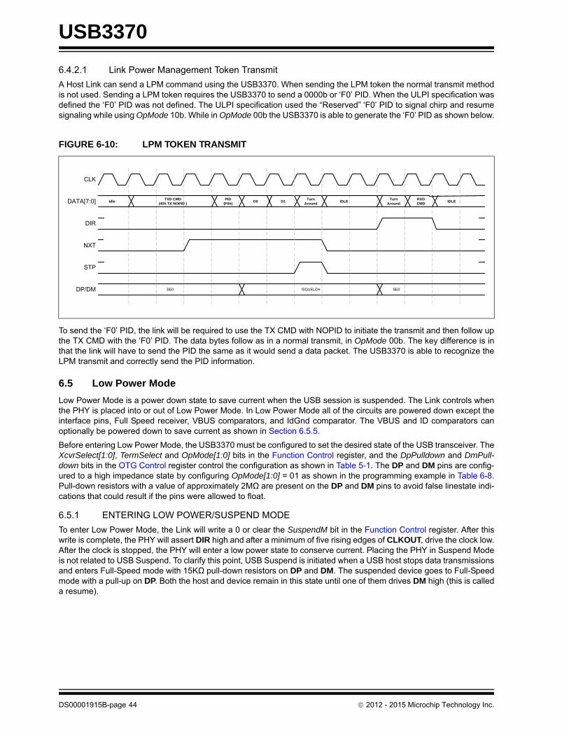
USB3370
6.4.2.1 Link Power Management Token Transmit
A Host Link can send a LPM command using the USB3370. When sending the LPM token the normal transmit methodis not used. Sending a LPM token requires the USB3370 to send a 0000b or ‘F0’ PID. When the ULPI specification wasdefined the ‘F0’ PID was not defined. The ULPI specification used the “Reserved” ‘F0’ PID to signal chirp and resumesignaling while using OpMode 10b. While in OpMode 00b the USB3370 is able to generate the ‘F0’ PID as shown below.
To send the ‘F0’ PID, the link will be required to use the TX CMD with NOPID to initiate the transmit and then follow upthe TX CMD with the ‘F0’ PID. The data bytes follow as in a normal transmit, in OpMode 00b. The key difference is inthat the link will have to send the PID the same as it would send a data packet. The USB3370 is able to recognize theLPM transmit and correctly send the PID information.
6.5 Low Power Mode
Low Power Mode is a power down state to save current when the USB session is suspended. The Link controls whenthe PHY is placed into or out of Low Power Mode. In Low Power Mode all of the circuits are powered down except theinterface pins, Full Speed receiver, VBUS comparators, and IdGnd comparator. The VBUS and ID comparators canoptionally be powered down to save current as shown in Section 6.5.5.
Before entering Low Power Mode, the USB3370 must be configured to set the desired state of the USB transceiver. TheXcvrSelect[1:0], TermSelect and OpMode[1:0] bits in the Function Control register, and the DpPulldown and DmPull-down bits in the OTG Control register control the configuration as shown in Table 5-1. The DP and DM pins are config-ured to a high impedance state by configuring OpMode[1:0] = 01 as shown in the programming example in Table 6-8.Pull-down resistors with a value of approximately 2MΩ are present on the DP and DM pins to avoid false linestate indi-cations that could result if the pins were allowed to float.
6.5.1 ENTERING LOW POWER/SUSPEND MODE
To enter Low Power Mode, the Link will write a 0 or clear the SuspendM bit in the Function Control register. After thiswrite is complete, the PHY will assert DIR high and after a minimum of five rising edges of CLKOUT, drive the clock low.After the clock is stopped, the PHY will enter a low power state to conserve current. Placing the PHY in Suspend Modeis not related to USB Suspend. To clarify this point, USB Suspend is initiated when a USB host stops data transmissionsand enters Full-Speed mode with 15KΩ pull-down resistors on DP and DM. The suspended device goes to Full-Speedmode with a pull-up on DP. Both the host and device remain in this state until one of them drives DM high (this is calleda resume).
FIGURE 6-10: LPM TOKEN TRANSMIT
DATA[7:0]
DP/DM
DIR
CLK
STP
NXT
TXD CMD (40h TX NOPID ) Idle
PID(F0h)
D1 IDLE
SE0 !SQUELCH SE0
Turn Around
RXD CMD
D0Turn
AroundIDLE
DS00001915B-page 44 2012 - 2015 Microchip Technology Inc.
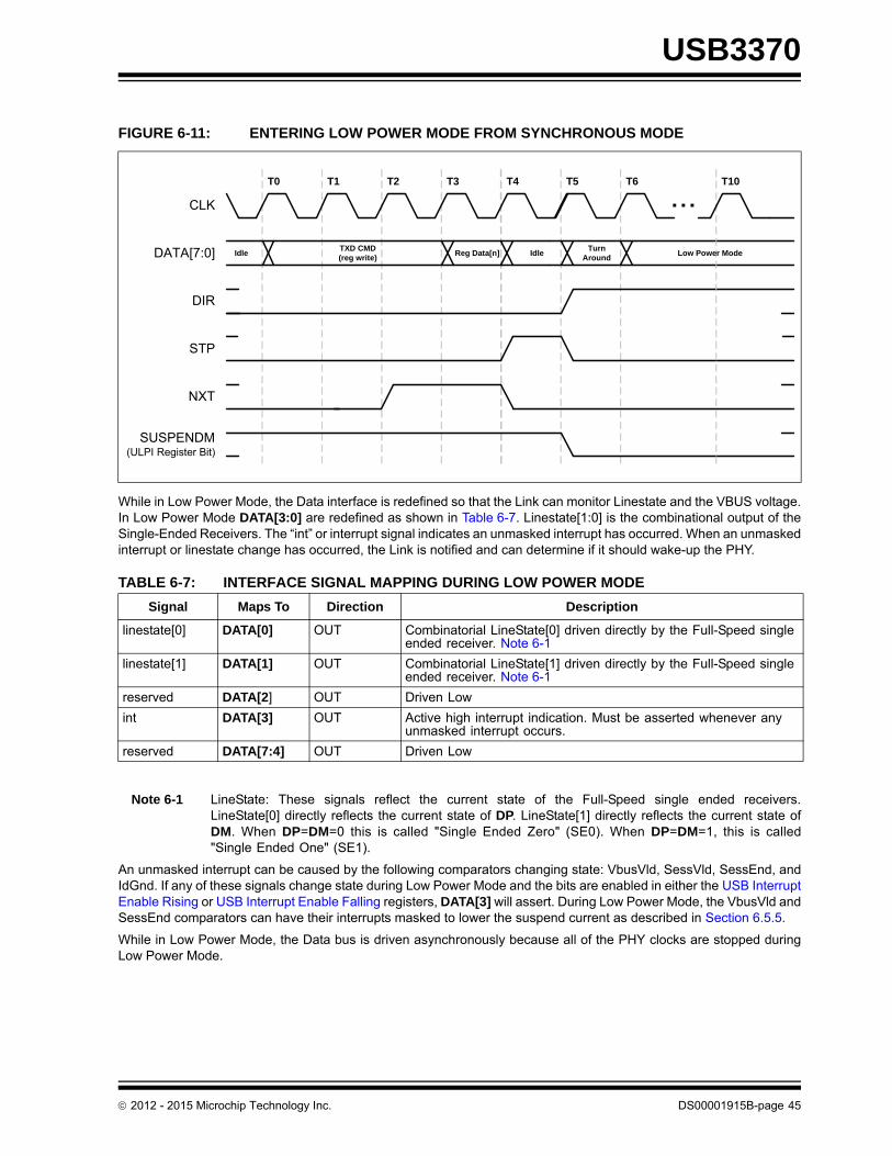
USB3370
While in Low Power Mode, the Data interface is redefined so that the Link can monitor Linestate and the VBUS voltage.In Low Power Mode DATA[3:0] are redefined as shown in Table 6-7. Linestate[1:0] is the combinational output of theSingle-Ended Receivers. The “int” or interrupt signal indicates an unmasked interrupt has occurred. When an unmaskedinterrupt or linestate change has occurred, the Link is notified and can determine if it should wake-up the PHY.
Note 6-1 LineState: These signals reflect the current state of the Full-Speed single ended receivers.LineState[0] directly reflects the current state of DP. LineState[1] directly reflects the current state ofDM. When DP=DM=0 this is called "Single Ended Zero" (SE0). When DP=DM=1, this is called"Single Ended One" (SE1).
An unmasked interrupt can be caused by the following comparators changing state: VbusVld, SessVld, SessEnd, andIdGnd. If any of these signals change state during Low Power Mode and the bits are enabled in either the USB InterruptEnable Rising or USB Interrupt Enable Falling registers, DATA[3] will assert. During Low Power Mode, the VbusVld andSessEnd comparators can have their interrupts masked to lower the suspend current as described in Section 6.5.5.
While in Low Power Mode, the Data bus is driven asynchronously because all of the PHY clocks are stopped duringLow Power Mode.
FIGURE 6-11: ENTERING LOW POWER MODE FROM SYNCHRONOUS MODE
TABLE 6-7: INTERFACE SIGNAL MAPPING DURING LOW POWER MODE
Signal Maps To Direction Description
linestate[0] DATA[0] OUT Combinatorial LineState[0] driven directly by the Full-Speed single ended receiver. Note 6-1
linestate[1] DATA[1] OUT Combinatorial LineState[1] driven directly by the Full-Speed single ended receiver. Note 6-1
reserved DATA[2] OUT Driven Low
int DATA[3] OUT Active high interrupt indication. Must be asserted whenever any unmasked interrupt occurs.
reserved DATA[7:4] OUT Driven Low
DIR
CLK
DATA[7:0]
STP
NXT
TXD CMD (reg write) Idle Reg Data[n] Idle
T0 T1 T2 T3 T5T4 T6 T10
TurnAround
Low Power Mode
SUSPENDM(ULPI Register Bit)
...
2012 - 2015 Microchip Technology Inc. DS00001915B-page 45
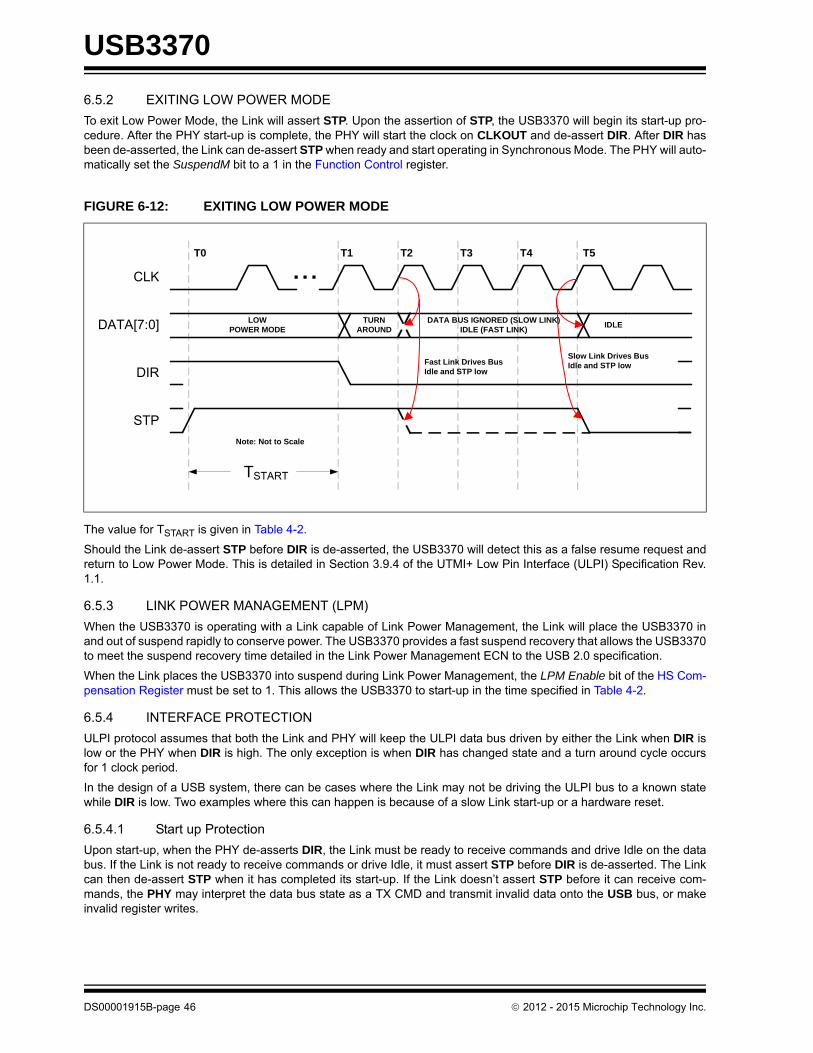
USB3370
6.5.2 EXITING LOW POWER MODE
To exit Low Power Mode, the Link will assert STP. Upon the assertion of STP, the USB3370 will begin its start-up pro-cedure. After the PHY start-up is complete, the PHY will start the clock on CLKOUT and de-assert DIR. After DIR hasbeen de-asserted, the Link can de-assert STP when ready and start operating in Synchronous Mode. The PHY will auto-matically set the SuspendM bit to a 1 in the Function Control register.
The value for TSTART is given in Table 4-2.
Should the Link de-assert STP before DIR is de-asserted, the USB3370 will detect this as a false resume request andreturn to Low Power Mode. This is detailed in Section 3.9.4 of the UTMI+ Low Pin Interface (ULPI) Specification Rev.1.1.
6.5.3 LINK POWER MANAGEMENT (LPM)
When the USB3370 is operating with a Link capable of Link Power Management, the Link will place the USB3370 inand out of suspend rapidly to conserve power. The USB3370 provides a fast suspend recovery that allows the USB3370to meet the suspend recovery time detailed in the Link Power Management ECN to the USB 2.0 specification.
When the Link places the USB3370 into suspend during Link Power Management, the LPM Enable bit of the HS Com-pensation Register must be set to 1. This allows the USB3370 to start-up in the time specified in Table 4-2.
6.5.4 INTERFACE PROTECTION
ULPI protocol assumes that both the Link and PHY will keep the ULPI data bus driven by either the Link when DIR islow or the PHY when DIR is high. The only exception is when DIR has changed state and a turn around cycle occursfor 1 clock period.
In the design of a USB system, there can be cases where the Link may not be driving the ULPI bus to a known statewhile DIR is low. Two examples where this can happen is because of a slow Link start-up or a hardware reset.
6.5.4.1 Start up Protection
Upon start-up, when the PHY de-asserts DIR, the Link must be ready to receive commands and drive Idle on the databus. If the Link is not ready to receive commands or drive Idle, it must assert STP before DIR is de-asserted. The Linkcan then de-assert STP when it has completed its start-up. If the Link doesn’t assert STP before it can receive com-mands, the PHY may interpret the data bus state as a TX CMD and transmit invalid data onto the USB bus, or makeinvalid register writes.
FIGURE 6-12: EXITING LOW POWER MODE
DIR
CLK
DATA[7:0]
STP
TURNAROUND LOW
POWER MODEDATA BUS IGNORED (SLOW LINK)
IDLE (FAST LINK)IDLE
T0 T1 T2 T3 T5T4
Slow Link Drives Bus Idle and STP lowFast Link Drives Bus
Idle and STP low
...
Note: Not to Scale
TSTART
DS00001915B-page 46 2012 - 2015 Microchip Technology Inc.
USB3370
When the USB3370 sends a RXCMD the Link is required to drive the data bus back to idle at the end of the turn aroundcycle. If the Link does not drive the databus to idle the USB3370 may take the information on the data bus as a TXCMDand transmit data on DP and DM until the Link asserts stop. If the ID pin is floated the last RXCMD from the USB3370will remain on the bus after DIR is de-asserted and the USB3370 will take this in as a TXCMD.
A Link should be designed to have the default POR state of the STP output high and the data bus tri-stated. TheUSB3370 has weak pull-downs on the data bus to prevent these inputs from floating when not driven. These resistorsare only used to prevent the ULPI interface from floating during events when the link ULPI pins may be tri-stated. Thestrength of the pull down resistors can be found in Table 4-4. The pull downs are not strong enough to pull the data buslow after a ULPI RXCMD, the Link must drive the data bus to idle after DIR is de-asserted.
In some cases, a Link may be software configured and not have control of its STP pin until after the PHY has started.In this case, the USB3370 has in internal pull-up on the STP input pad which will pull STP high while the Link’s STPoutput is tri-stated. The STP pull-up resistor is enabled on POR and can be disabled by setting the InterfaceProtectDis-able bit 7 of the Interface Control register.
The STP pull-up resistor will pull-up the Link’s STP input high until the Link configures and drives STP high. After theLink completes its start-up, STP can be synchronously driven low.
A Link design which drives STP high during POR can disable the pull-up resistor on STP by setting InterfaceProtect-Disable bit to 1. A motivation for this is to reduce the suspend current. In Low Power Mode, STP is held low, which woulddraw current through the pull-up resistor on STP.
6.5.4.2 Warm Reset
Designers should also consider the case of a warm restart of a Link with a PHY in Low Power Mode. After the PHYenters Low Power Mode, DIR is asserted and the clock is stopped. The USB3370 looks for STP to be asserted to re-start the clock and then resume normal synchronous operation.
Should the USB3370 be suspended in Low Power Mode, and the Link receives a hardware reset, the PHY must be ableto recover from Low Power Mode and start its clock. If the Link asserts STP on reset, the PHY will exit Low Power Modeand start its clock.
If the Link does not assert STP on reset, the interface protection pull-up can be used. When the Link is reset, its STPoutput will tri-state and the pull-up resistor will pull STP high, signaling the PHY to restart its clock.
6.5.5 MINIMIZING CURRENT IN LOW POWER MODE
In order to minimize the suspend current in Low Power Mode, the VBUS and ID comparators can be disabled to reducesuspend current. In Low Power Mode, the VbusVld and SessEnd comparators are not needed and can be disabled byclearing the associated bits in both the USB Interrupt Enable Rising and USB Interrupt Enable Falling registers. By dis-abling the interrupt in BOTH the rise and fall registers, the SessEnd and VbusVld comparators are turned off. TheIdFloatRise and IdFloatFall bits in Carkit Interrupt Enable register should also be disabled if they were set. When exitingLow Power Mode, the Link should immediately re-enable the VbusVld and SessEnd comparators if host or OTG func-tionality is required.
In addition to disabling the OTG comparators in Low Power Mode, the Link may choose to disable the Interface ProtectCircuit. By setting the InterfaceProtectDisable bit high in the Interface Control register, the Link can disable the pull-upresistor on STP. When RESETB is low the Interface Protect Circuit will be disabled.
6.6 Full Speed/Low Speed Serial Modes
The USB3370 includes two serial modes to support legacy Links which use either the 3pin or 6pin serial format. To entereither serial mode, the Link will need to write a 1 to the 6-pin FsLsSerialMode or the 3-pin FsLsSerialMode bits in theInterface control register. Serial Mode may be used to conserve power when attached to a device that is not capable ofoperating in Hi-Speed.
The serial modes are entered in the same manner as the entry into Low Power Mode. The Link writes the InterfaceControl register bit for the specific serial mode. The USB3370 will assert DIR and shut off the clock after at least fiveclock cycles. Then the data bus goes to the format of the serial mode selected. Before entering Serial Mode the Linkmust set the ULPI transceiver to the appropriate mode as defined in Table 5-1.
In ULPI Clock Output Mode, the PHY will shut off the 60MHz clock to conserve power. Should the Link need the 60MHzclock to continue during the serial mode of operation, the ClockSuspendM bit[3] of the Interface Control Register shouldbe set before entering a serial mode. If set, the 60 MHz clock will be present during serial modes.
2012 - 2015 Microchip Technology Inc. DS00001915B-page 47

USB3370
In serial mode, interrupts are possible from unmasked sources. The state of each interrupt source is sampled prior tothe assertion of DIR and this is compared against the asynchronous level from interrupt source.
Exiting the serial modes is the same as exiting Low Power Mode. The Link must assert STP to signal the PHY to exitserial mode. When the PHY can accept a command, DIR is de-asserted and the PHY will wait until the Link de-assertsSTP to resume synchronous ULPI operation. The RESETB pin can also be pulsed low to reset the USB3370 and returnit to Synchronous Mode.
6.6.1 3-PIN FS/LS SERIAL MODE
Three pin serial mode utilizes the data bus pins for the serial functions shown in Table 6-8.
6.6.2 6-PIN FS/LS SERIAL MODE
Six pin serial mode utilizes the data bus pins for the serial functions shown in Table 6-9.
6.7 Carkit Mode
The USB3370 includes Carkit Mode to support a USB UART Mode.
By entering Carkit Mode, the USB3370 current drain is minimized. The internal PLL is disabled and the 60MHz ULPICLKOUT will be stopped to conserve power by default. The Link may configure the 60MHz clock to continue by settingthe ClockSuspendM bit of the Interface Control register before entering Carkit Mode. If set, the 60 MHz clock will con-tinue during the Carkit Mode of operation.
In Carkit Mode, interrupts are possible if they have been enabled in the Carkit Interrupt Enable register. The state ofeach interrupt source is sampled prior to the assertion of DIR and this is compared against the asynchronous level frominterrupt source. In Carkit Mode, the Linestate signals are not available per the ULPI specification.
The ULPI interface is redefined to the following when Carkit Mode is entered.
TABLE 6-8: PIN DEFINITIONS IN 3 PIN SERIAL MODE
Signal Connected To Direction Description
tx_enable DATA[0] IN Active High transmit enable.
data DATA[1] I/O TX differential data on DP/DM when tx_enable is high.RX differential data from DP/DM when tx_enable is low.
SE0 DATA[2] I/O TX SE0 on DP/DM when tx_enable is high.RX SE0_b from DP/DM when tx_enable is low.
interrupt DATA[3] OUT Asserted when any unmasked interrupt occurs. Active high.
Reserved DATA[7:4] OUT Driven Low.
TABLE 6-9: PIN DEFINITIONS IN 6 PIN SERIAL MODE
Signal Connected To Direction Description
tx_enable DATA[0] IN Active High transmit enable.
tx_data DATA[1] IN Tx differential data on DP/DM when tx_enable is high.
tx_se0 DATA[2] IN Tx SE0 on DP/DM when tx_enable is high.
interrupt DATA[3] OUT Asserted when any unmasked interrupt occurs. Active high.
rx_dp DATA[4] OUT Single ended receive data on DP.
rx_dm DATA[5] OUT Single ended receive data on DM.
rx_rcv DATA[6] OUT Differential receive data from DP and DM.
Reserved DATA[7] OUT Driven Low.
DS00001915B-page 48 2012 - 2015 Microchip Technology Inc.
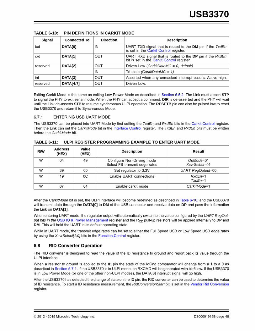
USB3370
Exiting Carkit Mode is the same as exiting Low Power Mode as described in Section 6.5.2. The Link must assert STPto signal the PHY to exit serial mode. When the PHY can accept a command, DIR is de-asserted and the PHY will waituntil the Link de-asserts STP to resume synchronous ULPI operation. The RESETB pin can also be pulsed low to resetthe USB3370 and return it to Synchronous Mode.
6.7.1 ENTERING USB UART MODE
The USB3370 can be placed into UART Mode by first setting the TxdEn and RxdEn bits in the Carkit Control register.Then the Link can set the CarkitMode bit in the Interface Control register. The TxdEn and RxdEn bits must be writtenbefore the CarkitMode bit.
After the CarkitMode bit is set, the ULPI interface will become redefined as described in Table 6-10, and the USB3370will transmit data through the DATA[0] to DM of the USB connector and receive data on DP and pass the informationthe Link on DATA[1].
When entering UART mode, the regulator output will automatically switch to the value configured by the UART RegOut-put bits in the USB IO & Power Management register and the RCD pull-up resistors will be applied internally to DP andDM. This will hold the UART in its default operating state.
While in UART mode, the transmit edge rates can be set to either the Full Speed USB or Low Speed USB edge ratesby using the XcvrSelect[1:0] bits in the Function Control register.
6.8 RID Converter Operation
The RID converter is designed to read the value of the ID resistance to ground and report back its value through theULPI interface.
When a resistor to ground is applied to the ID pin the state of the IdGnd comparator will change from a 1 to a 0 asdescribed in Section 5.7.1. If the USB3370 is in ULPI mode, an RXCMD will be generated with bit 6 low. If the USB3370is in Low Power Mode (or one of the other non-ULPI modes), the DATA[3] interrupt signal will go high.
After the USB3370 has detected the change of state on the ID pin, the RID converter can be used to determine the valueof ID resistance. To start a ID resistance measurement, the RidConversionStart bit is set in the Vendor Rid Conversionregister.
TABLE 6-10: PIN DEFINITIONS IN CARKIT MODE
Signal Connected To Direction Description
txd DATA[0] IN UART TXD signal that is routed to the DM pin if the TxdEn is set in the Carkit Control register.
rxd DATA[1] OUT UART RXD signal that is routed to the DP pin if the RxdEn bit is set in the Carkit Control register.
reserved DATA[2] OUT Driven Low (CarkitDataMC = 0, default)
IN Tri-state (CarkitDataMC = 1)
int DATA[3] OUT Asserted when any unmasked interrupt occurs. Active high.
reserved DATA[4:7] OUT Driven Low.
TABLE 6-11: ULPI REGISTER PROGRAMMING EXAMPLE TO ENTER UART MODE
R/WAddress
(HEX)Value(HEX)
Description Result
W 04 49 Configure Non-Driving modeSelect FS transmit edge rates
OpMode=01XcvrSelect=01
W 39 00 Set regulator to 3.3V UART RegOutput=00
W 19 0C Enable UART connections RxdEn=1TxdEn=1
W 07 04 Enable carkit mode CarkitMode=1
2012 - 2015 Microchip Technology Inc. DS00001915B-page 49
USB3370
The Link can use one of two methods to determine when the RID Conversion is complete. One method is polling theRidConversionStart bit as described in Section 7.1.3.3. The preferred method is to set the RidIntEn bit in the Vendor RidConversion register. When RidIntEn is set, an RXCMD will be generated after the RID conversion is complete. Asdescribed in Table 6-3, the alt_int bit of the RXCMD will be set.
After the RID Conversion is complete, the Link can read RidValue from the Vendor Rid Conversion register.
DS00001915B-page 50 2012 - 2015 Microchip Technology Inc.

USB3370
7.0 ULPI REGISTER MAP
7.1 ULPI Register Array
The USB3370 PHY implements all of the ULPI registers detailed in the ULPI revision 1.1 specification. The completeUSB3370 ULPI register set is shown in Table 7-1. All registers are 8 bits. This table also includes the default state ofeach register upon POR or de-assertion of RESETB, as described in Section 5.6.2. The RESET bit in the Function Con-trol Register does not reset the bits of the ULPI register array. The Link should not read or write to any registers notlisted in this table.
The USB3370 supports extended register access. The immediate register set (00-3Fh) can be accessed through eithera immediate address or an extended register address.
Note 7-1 Dynamically updates to reflect current status of interrupt sources.
TABLE 7-1: ULPI REGISTER MAP
Register NameDefault State
Address (6bit)
Read Write Set Clear
Vendor ID Low 24h 00h - - -
Vendor ID High 04h 01h - - -
Product ID Low 0Dh 02h - - -
Product ID High 00h 03h - - -
Function Control 41h 04-06h 04h 05h 06h
Interface Control 00h 07-09h 07h 08h 09h
OTG Control 06h 0A-0Ch 0Ah 0Bh 0Ch
USB Interrupt Enable Rising 1Fh 0D-0Fh 0Dh 0Eh 0Fh
USB Interrupt Enable Falling 1Fh 10-12h 10h 11h 12h
USB Interrupt Status (Note 7-1) 00h 13h - - -
USB Interrupt Latch 00h 14h - - -
Debug 00h 15h - - -
Scratch Register 00h 16-18h 16h 17h 18h
Carkit Control 00h 19-1Bh 19h 1Ah 1Bh
Reserved 00h 1Ch
Carkit Interrupt Enable 00h 1D-1Fh 1Dh 1Eh 1Fh
Carkit Interrupt Status 00h 20h - - -
Carkit Interrupt Latch 00h 21h - - -
Reserved 00h 22-30h
HS Compensation Register 00h 31h 31h - -
USB-IF Charger Detection 00h 32h 32h - -
Reserved 00h 33-35h
Vendor Rid Conversion 00h 36-38h 36h 37h 38h
USB IO & Power Management 04h 39-3Bh 39h 3Ah 3Bh
Reserved 00h 3C-3Fh
2012 - 2015 Microchip Technology Inc. DS00001915B-page 51

USB3370
7.1.1 ULPI REGISTER SET
The following registers are used for the ULPI interface.
7.1.1.1 Vendor ID Low
Address = 00h (read only)
7.1.1.2 Vendor ID High
Address = 01h (read only)
7.1.1.3 Product ID Low
Address = 02h (read only)
7.1.1.4 Product ID High
Address = 03h (read only)
7.1.1.5 Function Control
Address = 04-06h (read), 04h (write), 05h (set), 06h (clear)
Field Name Bit Access Default Description
Vendor ID Low 7:0 rd 24h MCHP Vendor ID
Field Name Bit Access Default Description
Vendor ID High 7:0 rd 04h MCHP Vendor ID
Field Name Bit Access Default Description
Product ID Low 7:0 rd 0Dh MCHP Product ID
Field Name Bit Access Default Description
Product ID High 7:0 rd 00h MCHP Product ID
Field Name Bit Access Default Description
XcvrSelect[1:0] 1:0 rd/w/s/c 01b Selects the required transceiver speed.00b: Enables HS transceiver01b: Enables FS transceiver10b: Enables LS transceiver11b: Enables FS transceiver for LS packets (FS preamble automatically pre-pended)
TermSelect 2 rd/w/s/c 0b Controls the DP and DM termination depending on XcvrSelect, OpMode, DpPulldown, and DmPulldown. The DP and DM termination is detailed in Table 5-1.
OpMode[1:0] 4:3 rd/w/s/c 00b Selects the required bit encoding style during transmit.00b: Normal Operation01b: Non-Driving10b: Disable bit-stuff and NRZI encoding11b: Reserved
Reset 5 rd/w/s/c 0b Active high transceiver reset. This reset does not reset the ULPI interface or register set. Automatically clears after reset is complete.
DS00001915B-page 52 2012 - 2015 Microchip Technology Inc.

USB3370
7.1.1.6 Interface Control
Address = 07-09h (read), 07h (write), 08h (set), 09h (clear)
7.1.1.7 OTG Control
Address = 0A-0Ch (read), 0Ah (write), 0Bh (set), 0Ch (clear)
SuspendM 6 rd/w/s/c 1b Active low PHY suspend. When cleared the PHY will enter Low Power Mode as detailed in Section 6.5. Automatically set when exiting Low Power Mode.
LPM Enable 7 rd/w/s/c 0b When enabled the PLL start-up time is shortened to allow fast start-up for LPM. The reduced PLL start-up time is achieved by bypassing the VCO process compensation which was done on initial start-up.
Field Name Bit Access Default Description
6-pin FsLsSerialMode 0 rd/w/s/c 0b When asserted the ULPI interface is redefined to the 6-pin Serial Mode. The PHY will automatically clear this bit when exiting serial mode.
3-pin FsLsSerialMode 1 rd/w/s/c 0b When asserted the ULPI interface is redefined to the 3-pin Serial Mode. The PHY will automatically clear this bit when exiting serial mode.
CarkitMode 2 rd/w/s/c 0b When asserted the ULPI interface is redefined to the Carkit interface. The PHY will automatically clear this bit when exiting Carkit Mode.
ClockSuspendM 3 rd/w/s/c 0b Enables Link to turn on 60MHz CLKOUT in Serial Mode or Carkit Mode.0b: Disable clock in serial or Carkit Mode.1b: Enable clock in serial or Carkit Mode.
AutoResume 4 rd/w/s/c 0b Only applicable in Host mode. Enables the PHY to automatically transmit resume signaling. This function is detailed in Section 6.4.1.4.
IndicatorComplement 5 rd/w/s/c 0b Inverts the EXTVBUS signal. This function is detailed in Section 5.7.2.
IndicatorPassThru 6 rd/w/s/c 0b Disables and’ing the internal VBUS comparator with the EXTVBUS signal when asserted. This function is detailed in Section 5.7.2.
InterfaceProtectDisable 7 rd/w/s/c 0b Used to disable the integrated STP pull-up resistor used for interface protection. This function is detailed in Section 6.5.4.
Field Name Bit Access Default Description
IdPullup 0 rd/w/s/c 0b Connects a 100kΩ pull-up resistor from the ID pin to VDD330b: Disables the pull-up resistor1b: Enables the pull-up resistor
DpPulldown 1 rd/w/s/c 1b Enables the 15k Ohm pull-down resistor on DP.0b: Pull-down resistor not connected1b: Pull-down resistor connected
DmPulldown 2 rd/w/s/c 1b Enables the 15k Ohm pull-down resistor on DM.0b: Pull-down resistor not connected1b: Pull-down resistor connected
Field Name Bit Access Default Description
2012 - 2015 Microchip Technology Inc. DS00001915B-page 53
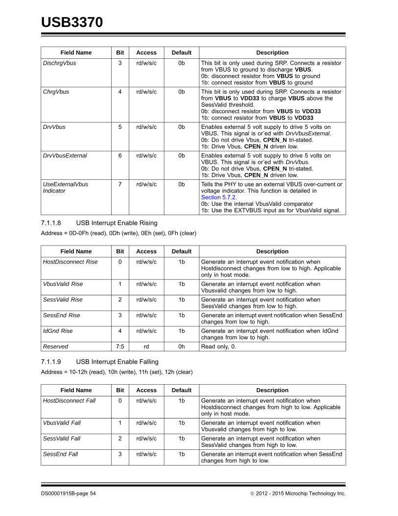
USB3370
7.1.1.8 USB Interrupt Enable Rising
Address = 0D-0Fh (read), 0Dh (write), 0Eh (set), 0Fh (clear)
7.1.1.9 USB Interrupt Enable Falling
Address = 10-12h (read), 10h (write), 11h (set), 12h (clear)
DischrgVbus 3 rd/w/s/c 0b This bit is only used during SRP. Connects a resistor from VBUS to ground to discharge VBUS. 0b: disconnect resistor from VBUS to ground1b: connect resistor from VBUS to ground
ChrgVbus 4 rd/w/s/c 0b This bit is only used during SRP. Connects a resistor from VBUS to VDD33 to charge VBUS above the SessValid threshold.0b: disconnect resistor from VBUS to VDD331b: connect resistor from VBUS to VDD33
DrvVbus 5 rd/w/s/c 0b Enables external 5 volt supply to drive 5 volts on VBUS. This signal is or’ed with DrvVbusExternal.0b: Do not drive Vbus, CPEN_N tri-stated.1b: Drive Vbus, CPEN_N driven low.
DrvVbusExternal 6 rd/w/s/c 0b Enables external 5 volt supply to drive 5 volts on VBUS. This signal is or’ed with DrvVbus.0b: Do not drive Vbus, CPEN_N tri-stated.1b: Drive Vbus, CPEN_N driven low.
UseExternalVbusIndicator
7 rd/w/s/c 0b Tells the PHY to use an external VBUS over-current or voltage indicator. This function is detailed in Section 5.7.2.0b: Use the internal VbusValid comparator1b: Use the EXTVBUS input as for VbusValid signal.
Field Name Bit Access Default Description
HostDisconnect Rise 0 rd/w/s/c 1b Generate an interrupt event notification when Hostdisconnect changes from low to high. Applicable only in host mode.
VbusValid Rise 1 rd/w/s/c 1b Generate an interrupt event notification when Vbusvalid changes from low to high.
SessValid Rise 2 rd/w/s/c 1b Generate an interrupt event notification when SessValid changes from low to high.
SessEnd Rise 3 rd/w/s/c 1b Generate an interrupt event notification when SessEnd changes from low to high.
IdGnd Rise 4 rd/w/s/c 1b Generate an interrupt event notification when IdGnd changes from low to high.
Reserved 7:5 rd 0h Read only, 0.
Field Name Bit Access Default Description
HostDisconnect Fall 0 rd/w/s/c 1b Generate an interrupt event notification when Hostdisconnect changes from high to low. Applicable only in host mode.
VbusValid Fall 1 rd/w/s/c 1b Generate an interrupt event notification when Vbusvalid changes from high to low.
SessValid Fall 2 rd/w/s/c 1b Generate an interrupt event notification when SessValid changes from high to low.
SessEnd Fall 3 rd/w/s/c 1b Generate an interrupt event notification when SessEnd changes from high to low.
Field Name Bit Access Default Description
DS00001915B-page 54 2012 - 2015 Microchip Technology Inc.

USB3370
7.1.1.10 USB Interrupt Status
Address = 13h (read only)
This register dynamically updates to reflect current status of interrupt sources.
7.1.1.11 USB Interrupt Latch
Address = 14h (read only with auto clear)
Note 7-2 rd: Read Only with auto clear.
IdGnd Fall 4 rd/w/s/c 1b Generate an interrupt event notification when IdGnd changes from high to low.
Reserved 7:5 rd 0h Read only, 0.
Field Name Bit Access Default Description
HostDisconnect 0
rd(read only)
0b Current value of the UTMI+ HS Hostdisconnect output. Applicable only in host mode.
VbusValid 1 0b Current value of the UTMI+ Vbusvalid output. If VbusValid Rise and VbusValid Fall are set this register will read 0.
SessValid 2 0b Current value of the UTMI+ SessValid output. This register will always read the current status of the Session Valid comparator regardless of the SessValid Rise and SessValid Fall settings.
SessEnd 3 0b Current value of the UTMI+ SessEnd output. If SessEnd Rise and SessEnd Fall are set this register will read 0.
IdGnd 4 0b Current value of the UTMI+ IdGnd output.
Reserved 7:5 0h Read only, 0.
Note: The default value is only valid after POR. When the register is read it will match the current status of thecomparators at the moment the register is read.
Field Name Bit Access Default Description
HostDisconnect Latch 0
rd(Note 7-2)
0b Set to 1b by the PHY when an unmasked event occurs on Hostdisconnect. Cleared when this register is read. Applicable only in host mode.
VbusValid Latch 1 0b Set to 1b by the PHY when an unmasked event occurs on VbusValid. Cleared when this register is read.
SessValid Latch 2 0b Set to 1b by the PHY when an unmasked event occurs on SessValid. Cleared when this register is read.
SessEnd Latch 3 0b Set to 1b by the PHY when an unmasked event occurs on SessEnd. Cleared when this register is read.
IdGnd Latch 4 0b Set to 1b by the PHY when an unmasked event occurs on IdGnd. Cleared when this register is read.
Reserved 7:5 rd 0h Read only, 0.
Field Name Bit Access Default Description
2012 - 2015 Microchip Technology Inc. DS00001915B-page 55

USB3370
7.1.1.12 Debug
Address = 15h (read only)
7.1.1.13 Scratch Register
Address = 16-18h (read), 16h (write), 17h (set), 18h (clear)
7.1.2 CARKIT CONTROL REGISTERS
The following registers are used to set-up and enable the USB UART functions.
7.1.2.1 Carkit Control
Address = 19-1Bh (read), 19h (write), 1Ah (set), 1Bh (clear)
This register is used to program the USB3370 into and out of the Carkit Mode. When entering the UART mode the Linkmust first set the desired TxdEn and the RxdEn bits and then transition to Carkit Mode by setting the CarkitMode bit inthe Interface Control Register. When RxdEn is not set then the DATA[1] pin is held to a logic high.
7.1.2.2 Carkit Interrupt Enable
Address = 1D-1Fh (read), 1Dh (write), 1Eh (set), 1Fh (clear)
Field Name Bit Access Default Description
Linestate[1:0] 1:0 rd 00b Contains the current value of Linestate[1:0].
Reserved 7:2 rd 000000b Read only, 0.
Field Name Bit Access Default Description
Scratch 7:0 rd/w/s/c 00h Empty register byte for testing purposes. Software can read, write, set, and clear this register and the PHY functionality will not be affected.
Field Name Bit Access Default Description
CarkitPwr 0 rd 0b Read only, 0.
IdGndDrv 1 rd/w/s/c 0b Drives ID pin to ground
TxdEn 2 rd/w/s/c 0b Connects UART TXD (DATA[0]) to DM
RxdEn 3 rd/w/s/c 0b Connects UART RXD (DATA[1]) to DP
Reserved 4 rd/w/s/c 0b
Reserved 5 rd/w/s/c 0b
Reserved 6 rd/w/s/c 0b
CarkitDataMC 7 rd/w/s/c 0b When set the UPLI DATA[2] pin is changed from a driven 0 to tri-state, when carkit mode is entered.
Field Name Bit Access Default Description
IdFloatRise 0 rd/w/s/c 0b When enabled an interrupt will be generated on the alt_int of the RXCMD byte when the ID pin transitions from non-floating to floating. The IdPullup bit in the OTG Control register should be set.
IdFloatFall 1 rd/w/s/c 0b When enabled an interrupt will be generated on the alt_int of the RXCMD byte when the ID pin transitions from floating to non-floating. The IdPullup bit in the OTG Control register should be set.
VdatDetIntEn 2 rd/w/s/c 0b When enabled an interrupt will be generated on the alt_int of the RXCMD byte when the VDAT_DET Comparator changes state.
DS00001915B-page 56 2012 - 2015 Microchip Technology Inc.
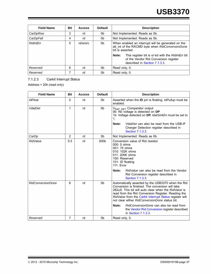
USB3370
7.1.2.3 Carkit Interrupt Status
Address = 20h (read only)
CarDpRise 3 rd 0b Not Implemented. Reads as 0b.
CarDpFall 4 rd 0b Not Implemented. Reads as 0b.
RidIntEn 5 rd/w/s/c 0b When enabled an interrupt will be generated on the alt_int of the RXCMD byte when RidConversionDone bit is asserted.
Note: This register bit is or’ed with the RidIntEn bit of the Vendor Rid Conversion register described in Section 7.1.3.3.
Reserved 6 rd 0b Read only, 0.
Reserved 7 rd 0b Read only, 0.
Field Name Bit Access Default Description
IdFloat 0 rd 0b Asserted when the ID pin is floating. IdPullup must be enabled.
VdatDet 1 rd 0b VDAT_DET Comparator output0b: No voltage is detected on DP1b: Voltage detected on DP, IdatSinkEn must be set to 1.
Note: VdatDet can also be read from the USB-IF Charger Detection register described in Section 7.1.3.3.
CarDp 2 rd 0b Not Implemented. Reads as 0b.
RidValue 5:3 rd 000b Conversion value of Rid resistor000: 0 ohms001: 75 ohms010: 102K ohms011: 200K ohms100: Reserved101: ID floating111: Error
Note: RidValue can also be read from the Vendor Rid Conversion register described in Section 7.1.3.3.
RidConversionDone 6 rd 0b Automatically asserted by the USB3370 when the Rid Conversion is finished. The conversion will take 282uS. This bit will auto clear when the RidValue is read from the Rid Conversion Register. Reading the RidValue from the Carkit Interrupt Status register will not clear either RidConversionDone status bit.
Note: RidConversionDone can also be read from the Vendor Rid Conversion register described in Section 7.1.3.3.
Reserved 7 rd 0b Read only, 0.
Field Name Bit Access Default Description
2012 - 2015 Microchip Technology Inc. DS00001915B-page 57
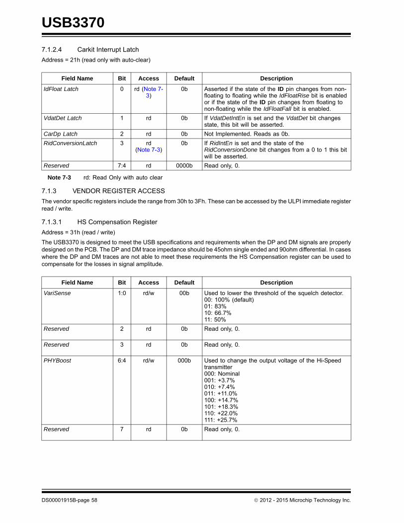
USB3370
7.1.2.4 Carkit Interrupt Latch
Address = 21h (read only with auto-clear)
Note 7-3 rd: Read Only with auto clear
7.1.3 VENDOR REGISTER ACCESS
The vendor specific registers include the range from 30h to 3Fh. These can be accessed by the ULPI immediate registerread / write.
7.1.3.1 HS Compensation Register
Address = 31h (read / write)
The USB3370 is designed to meet the USB specifications and requirements when the DP and DM signals are properlydesigned on the PCB. The DP and DM trace impedance should be 45ohm single ended and 90ohm differential. In caseswhere the DP and DM traces are not able to meet these requirements the HS Compensation register can be used tocompensate for the losses in signal amplitude.
Field Name Bit Access Default Description
IdFloat Latch 0 rd (Note 7-3)
0b Asserted if the state of the ID pin changes from non-floating to floating while the IdFloatRise bit is enabled or if the state of the ID pin changes from floating to non-floating while the IdFloatFall bit is enabled.
VdatDet Latch 1 rd 0b If VdatDetIntEn is set and the VdatDet bit changes state, this bit will be asserted.
CarDp Latch 2 rd 0b Not Implemented. Reads as 0b.
RidConversionLatch 3 rd(Note 7-3)
0b If RidIntEn is set and the state of the RidConversionDone bit changes from a 0 to 1 this bit will be asserted.
Reserved 7:4 rd 0000b Read only, 0.
Field Name Bit Access Default Description
VariSense 1:0 rd/w 00b Used to lower the threshold of the squelch detector.00: 100% (default)01: 83%10: 66.7%11: 50%
Reserved 2 rd 0b Read only, 0.
Reserved 3 rd 0b Read only, 0.
PHYBoost 6:4 rd/w 000b Used to change the output voltage of the Hi-Speed transmitter000: Nominal001: +3.7%010: +7.4%011: +11.0%100: +14.7%101: +18.3%110: +22.0%111: +25.7%
Reserved 7 rd 0b Read only, 0.
DS00001915B-page 58 2012 - 2015 Microchip Technology Inc.
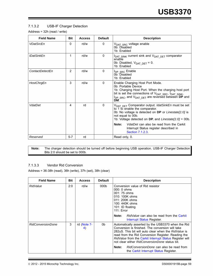
USB3370
7.1.3.2 USB-IF Charger Detection
Address = 32h (read / write)
7.1.3.3 Vendor Rid Conversion
Address = 36-38h (read), 36h (write), 37h (set), 38h (clear)
Field Name Bit Access Default Description
VDatSrcEn 0 rd/w 0 VDAT_SRC voltage enable0b: Disabled1b: Enabled
IDatSinkEn 1 rd/w 0 IDAT_SINK current sink and VDAT_DET comparator enable0b: Disabled, VDAT_DET = 0.1b: Enabled
ContactDetectEn 2 rd/w 0 IDP_SRC Enable0b: Disabled1b: Enabled
HostChrgEn 3 rd/w 0 Enable Charging Host Port Mode.0b: Portable Device1b: Charging Host Port. When the charging host port bit is set the connections of VDAT_SRC, IDAT_SINK, IDP_SRC, and VDAT_DET are reversed between DP and DM.
VdatDet 4 rd 0 VDAT_DET Comparator output. IdatSinkEn must be set to 1 to enable the comparator.0b: No voltage is detected on DP or Linestate[1:0] is not equal to 00b.1b: Voltage detected on DP, and Linestate[1:0] = 00b.
Note: VdatDet can also be read from the Carkit Interrupt Status register described in Section 7.1.2.3.
Reserved 5-7 rd Read only, 0.
Note: The charger detection should be turned off before beginning USB operation. USB-IF Charger DetectionBits 2:0 should be set to 000b.
Field Name Bit Access Default Description
RidValue 2:0 rd/w 000b Conversion value of Rid resistor000: 0 ohms001: 75 ohms010: 100K ohms011: 200K ohms100: 440K ohms101: ID floating111: Error
Note: RidValue can also be read from the Carkit Interrupt Status Register.
RidConversionDone 3 rd (Note 7-4)
0b Automatically asserted by the USB3370 when the Rid Conversion is finished. The conversion will take 282uS. This bit will auto clear when the RidValue is read from the Rid Conversion Register. Reading the RidValue from the Carkit Interrupt Status Register will not clear either RidConversionDone status bit.
Note: RidConversionDone can also be read from the Carkit Interrupt Status Register.
2012 - 2015 Microchip Technology Inc. DS00001915B-page 59

USB3370
Note 7-4 rd: Read Only with auto clear.
7.1.3.4 USB IO & Power Management
Address = 39-3Bh (read), 39h (write), 3Ah (set), 3Bh (clear)
RidConversionStart 4 rd/w/s/c 0b When this bit is asserted either through a register write or set, the Rid converter will read the value of the ID resistor. When the conversion is complete this bit will auto clear.
Reserved 5 rd/w/s/c 0b This bit must remain at 0.
RidIntEn 6 rd/w/s/c 0b When enabled an interrupt will be generated on the alt_int of the RXCMD byte when RidConversionDone bit is asserted.
Note: This register bit is or’ed with the RidIntEn bit of the Carkit Interrupt Status register.
Reserved 7 rd 0b Read only, 0.
Field Name Bit Access Default Description
Reserved 0 rd/w/s/c 0b Read only, 0.
SwapDP/DM 1 rd/w/s/c 0b When asserted, the DP and DM pins of the USB transceiver are swapped. This bit can be used to prevent crossing the DP/DM traces on the board. In UART mode, it swaps the routing to the DP and DM pins.
UART RegOutput 3:2 rd/w/s/c 01b Controls the output voltage of the VBAT to VDD33 regulator in UART mode. When the PHY is switched from USB mode to UART mode regulator output will automatically change to the value specified in this register when TxdEn is asserted.00: 3.3V01: 3.0V (default)10: 2.75V11: 2.5V
ChargerPullupEnDP 4 rd/w/s/c 0b Enables the RCD Pull-up resistor on the DP pin. (The pull-up is automatically enabled in UART mode)
ChargerPullupEnDM 5 rd/w/s/c 0b Enables the RCD Pull-up resistor on the DM pin. (The pull-up is automatically enabled in UART mode)
USB RegOutput 7:6 rd/w/s/c 00b Controls the output voltage of the VBAT to VDD33 regulator in USB mode. When the PHY is in Synchronous Mode, Serial Mode, or Low Power Mode, the regulator output will be the value specified in this register.00: 3.3V (default)01: 3.0V10: 2.75V11: 2.5V
Field Name Bit Access Default Description
DS00001915B-page 60 2012 - 2015 Microchip Technology Inc.

USB3370
8.0 APPLICATION NOTES
8.1 Application Diagrams
The USB3370 requires few external components as shown in the application diagrams. The USB 2.0 Specificationrestricts the voltage at the VBUS pin to a maximum value of 5.25V. In some applications, the voltage will exceed thislimit, so the USB3370 provides an integrated over voltage protection circuit. The over voltage protection circuit workswith an external resistor (RVBUS) to lower the voltage at the VBUS pin.
TABLE 8-1: COMPONENT VALUES IN APPLICATION DIAGRAMS
ReferenceDesignator
Value Description Notes
COUT See Table 4-10 Bypass capacitor to ground (<1Ω ESR) for regulator stability.
Place as close as possible to the PHY.
CVBUS See Table 8-2 Capacitor to ground required by the USB Specification. Microchip recommends <1Ω ESR.
Place near the USB connector.
CBYP System dependent.
Bypass capacitor to ground. Typical values used are 0.1 or 0.01 μF.
Place as close as possible to the PHY.
CDC_LOAD System dependent.
The USB connector housing may be AC-coupled to the device ground.
Industry convention is to ground only the host side of the cable shield.
RVBUS 1kΩ or 20kΩ Series resistor to work with internal over voltage protection.
See Section 5.7.3.4 for information regarding power dissipation.
RBIAS 10kΩ (±1%) Series resistor to establish reference voltage.
See Section 5.3 for information regarding power dissipation.
TABLE 8-2: CAPACITANCE VALUES AT VBUS OF USB CONNECTOR
MODE MIN Value MAX Value
Host 120μF
Device 1μF 10μF
OTG 1μF 6.5μF
2012 - 2015 Microchip Technology Inc. DS00001915B-page 61

USB3370
FIGURE 8-1: USB3370 APPLICATION DIAGRAM (HOST CONFIGURED FOR ULPI CLOCK INPUT MODE)
5V VBUS
VBAT
VDD33
ID
DM
DP
GND
USB Receptacle
DM
DP
ID
SHIELD
GND
VBUS
COUT
3.0-5.5VSupply
CBYP
RVBUS
The capacitor CVBUS
must be installed on this side of RVBUS.
CVBUS
RVBUS must be installed to enable overvoltage protection of the VBUS pin.
CPEN_N
Link Controller
DIRNXTSTP
CLKIN
DATA7DATA6DATA5DATA4DATA3DATA2
DATA0DATA1
RESETB
RBIAS
DIRNXTSTP
CLKOUT
DATA7DATA6DATA5DATA4DATA3DATA2
DATA0DATA1
RESETB
RBIAS
VDD18COUT
VDDIO
CBYP
VDDIO Supply
CLOAD
Resonator
Crystaland Caps
- or -REFCLK
XO
For Host applications (non-OTG), the ID pin should be connected to GND.
EXTVBUS
VBUS Switch
OUT
EN
IN
FAULT
DS00001915B-page 62 2012 - 2015 Microchip Technology Inc.

USB3370
FIGURE 8-2: USB3370 APPLICATION DIAGRAM (DEVICE CONFIGURED FOR ULPI CLOCK OUTPUT MODE)
3.0-5.5VSupply
RVBUS must be installed to enable overvoltage protection of the VBUS pin.
CDC_BLOCK
The capacitor CVBUS
must be installed on this side of RVBUS.
Link Controller
DIRNXTSTP
CLKIN
DATA7DATA6DATA5DATA4DATA3DATA2
DATA0DATA1
RESETB
REFCLKUSB Receptacle
DM
DP
VBUS
SHIELD
GND
RBIAS
DIRNXTSTP
CLKOUT
DATA7DATA6DATA5DATA4DATA3DATA2
DATA0DATA1
RESETB
VDD33
DM
DP
GND
COUT
COUT
CBYP
RVBUS
CVBUS
VDDIO
CBYP
VDDIO Supply
CPEN_N
XO
EXTVBUS
ID
REFCLK
VBUS
VDD18
RBIAS
VBAT
2012 - 2015 Microchip Technology Inc. DS00001915B-page 63
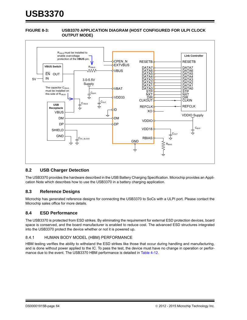
USB3370
8.2 USB Charger Detection
The USB3370 provides the hardware described in the USB Battery Charging Specification. Microchip provides an Appli-cation Note which describes how to use the USB3370 in a battery charging application.
8.3 Reference Designs
Microchip has generated reference designs for connecting the USB3370 to SoCs with a ULPI port. Please contact theMicrochip sales office for more details.
8.4 ESD Performance
The USB3370 is protected from ESD strikes. By eliminating the requirement for external ESD protection devices, boardspace is conserved, and the board manufacturer is enabled to reduce cost. The advanced ESD structures integratedinto the USB3370 protect the device whether or not it is powered up.
8.4.1 HUMAN BODY MODEL (HBM) PERFORMANCE
HBM testing verifies the ability to withstand the ESD strikes like those that occur during handling and manufacturing,and is done without power applied to the IC. To pass the test, the device must have no change in operation or perfor-mance due to the event. The USB3370 HBM performance is detailed in Table 4-12.
FIGURE 8-3: USB3370 APPLICATION DIAGRAM (HOST CONFIGURED FOR ULPI CLOCK OUTPUT MODE)
3.0-5.5VSupply
RVBUS must be installed to enable overvoltage protection of the VBUS pin.
CDC_BLOCK
The capacitor CVBUS
must be installed on this side of RVBUS.
Link Controller
DIRNXTSTP
CLKIN
DATA7DATA6DATA5DATA4DATA3DATA2
DATA0DATA1
RESETB
REFCLKUSB Receptacle
DM
DP
VBUS
SHIELD
GND
RBIAS
DIRNXTSTP
CLKOUT
DATA7DATA6DATA5DATA4DATA3DATA2
DATA0DATA1
RESETB
VDD33
DM
DP
GND
COUT
COUT
CBYP
RVBUS
CVBUS
VDDIO
CBYP
VDDIO Supply
CPEN_N
XO
EXTVBUS
IDREFCLK
VBUSVBUS Switch
OUTENIN5V
RBIAS
VDD18
VBAT
DS00001915B-page 64 2012 - 2015 Microchip Technology Inc.
USB3370
8.4.2 EN/IEC 61000-4-2 PERFORMANCE
The EN/IEC 61000-4-2 ESD specification is an international standard that addresses system-level immunity to ESDstrikes while the end equipment is operational. In contrast, the HBM ESD tests are performed at the device level withthe device powered down.
Microchip contracts with Independent laboratories to test the USB3370 to EN/IEC 61000-4-2 in a working system.Reports are available upon request. Please contact your Microchip representative, and request information on 3rd partyESD test results. The reports show that systems designed with the USB3370 can safely provide the ESD performanceshown in Table 4-12 without additional board level protection.
In addition to defining the ESD tests, EN/IEC 61000-4-2 also categorizes the impact to equipment operation when thestrike occurs (ESD Result Classification). The USB3370 maintains an ESD Result Classification 1 or 2 when subjectedto an EN/IEC 61000-4-2 (level 4) ESD strike.
Both air discharge and contact discharge test techniques for applying stress conditions are defined by the EN/IEC61000-4-2 ESD document.
8.4.2.1 Air Discharge
To perform this test, a charged electrode is moved close to the system being tested until a spark is generated. This testis difficult to reproduce because the discharge is influenced by such factors as humidity, the speed of approach of theelectrode, and construction of the test equipment.
8.4.2.2 Contact Discharge
The uncharged electrode first contacts the USB connector to prepare this test, and then the probe tip is energized. Thisyields more repeatable results, and is the preferred test method. The independent test laboratories contracted by Micro-chip provide test results for both types of discharge methods.
2012 - 2015 Microchip Technology Inc. DS00001915B-page 65

USB3370
9.0 PACKAGE OUTLINE
FIGURE 9-1: USB3370 32-PIN QFN, 5X5MM BODY, 0.5MM PITCH
Not
e: F
or th
e m
ost c
urre
nt p
acka
ge d
raw
ings
, se
e th
e M
icro
chip
Pac
kagi
ng S
peci
ficat
ion
at
http
://w
ww
.mic
roch
ip.c
om/p
acka
ging
DS00001915B-page 66 2012 - 2015 Microchip Technology Inc.

USB3370
FIGURE 9-1: USB3370 32-PIN QFN, 5X5MM BODY, 0.5MM PITCH (CONTINUED)
Not
e: F
or th
e m
ost c
urre
nt p
acka
ge d
raw
ings
, se
e th
e M
icro
chip
Pac
kagi
ng S
peci
ficat
ion
at
http
://w
ww
.mic
roch
ip.c
om/p
acka
ging
2012 - 2015 Microchip Technology Inc. DS00001915B-page 67

USB3370
FIGURE 9-2: 32QFN, 5X5 TAPE AND REEL
DS00001915B-page 68 2012 - 2015 Microchip Technology Inc.
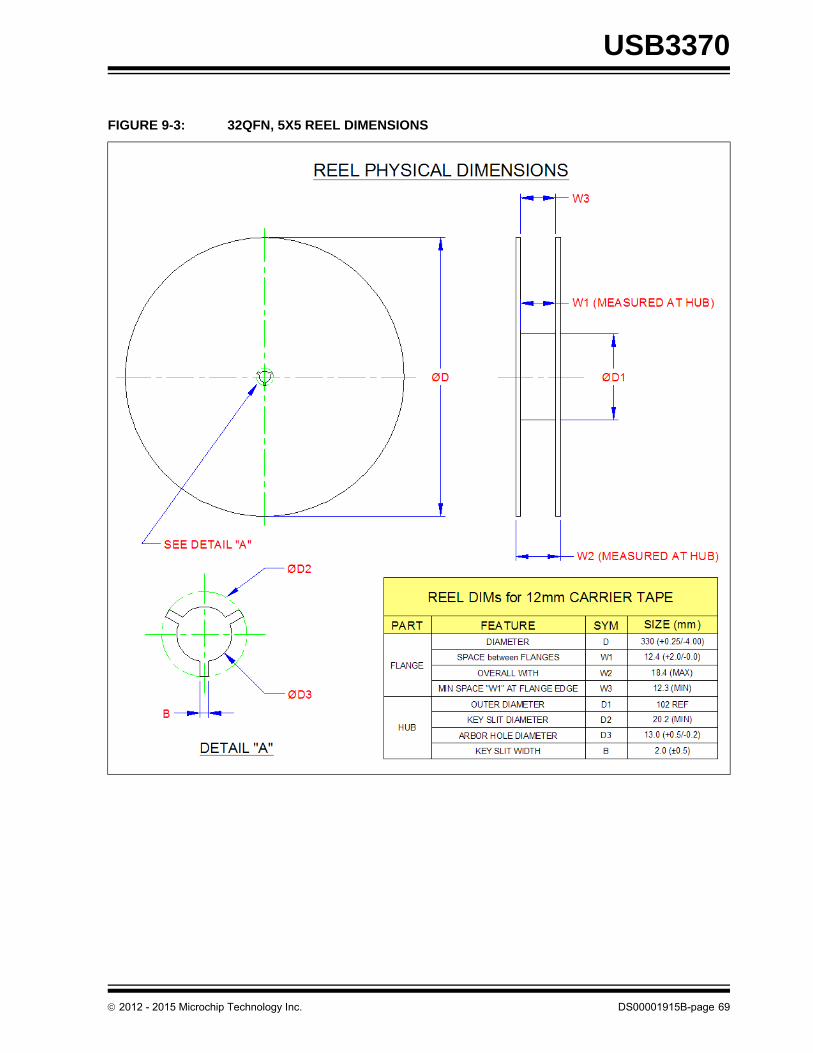
USB3370
FIGURE 9-3: 32QFN, 5X5 REEL DIMENSIONS
2012 - 2015 Microchip Technology Inc. DS00001915B-page 69
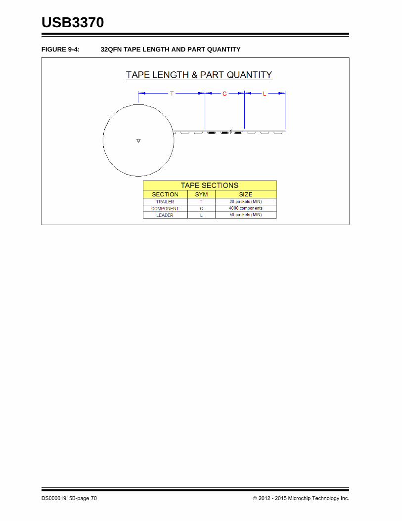
USB3370
FIGURE 9-4: 32QFN TAPE LENGTH AND PART QUANTITY
DS00001915B-page 70 2012 - 2015 Microchip Technology Inc.
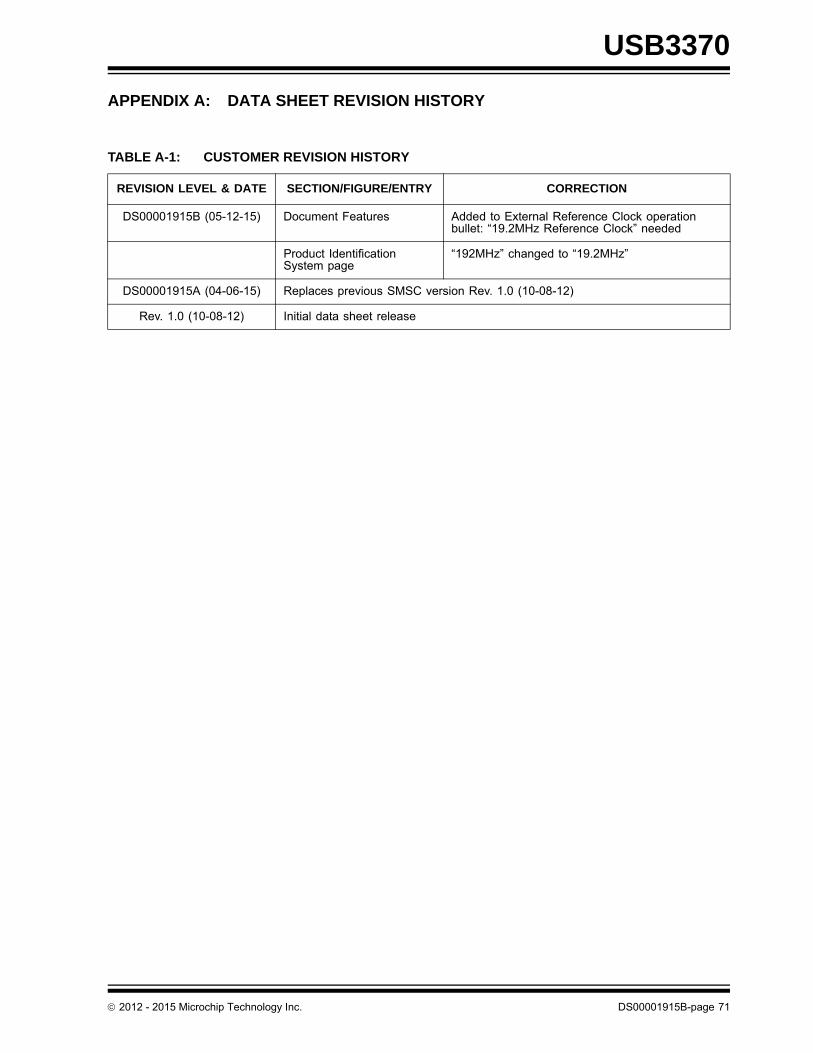
2012 - 2015 Microchip Technology Inc. DS00001915B-page 71
USB3370
APPENDIX A: DATA SHEET REVISION HISTORY
TABLE A-1: CUSTOMER REVISION HISTORY
REVISION LEVEL & DATE SECTION/FIGURE/ENTRY CORRECTION
DS00001915B (05-12-15) Document Features Added to External Reference Clock operation bullet: “19.2MHz Reference Clock” needed
Product Identification System page
“192MHz” changed to “19.2MHz”
DS00001915A (04-06-15) Replaces previous SMSC version Rev. 1.0 (10-08-12)
Rev. 1.0 (10-08-12) Initial data sheet release
USB3370
DS00001915B-page 72 2012 - 2015 Microchip Technology Inc.
THE MICROCHIP WEB SITE
Microchip provides online support via our WWW site at www.microchip.com. This web site is used as a means to makefiles and information easily available to customers. Accessible by using your favorite Internet browser, the web site con-tains the following information:
• Product Support – Data sheets and errata, application notes and sample programs, design resources, user’s guides and hardware support documents, latest software releases and archived software
• General Technical Support – Frequently Asked Questions (FAQ), technical support requests, online discussion groups, Microchip consultant program member listing
• Business of Microchip – Product selector and ordering guides, latest Microchip press releases, listing of semi-nars and events, listings of Microchip sales offices, distributors and factory representatives
CUSTOMER CHANGE NOTIFICATION SERVICE
Microchip’s customer notification service helps keep customers current on Microchip products. Subscribers will receivee-mail notification whenever there are changes, updates, revisions or errata related to a specified product family ordevelopment tool of interest.
To register, access the Microchip web site at www.microchip.com. Under “Support”, click on “Customer Change Notifi-cation” and follow the registration instructions.
CUSTOMER SUPPORT
Users of Microchip products can receive assistance through several channels:
• Distributor or Representative
• Local Sales Office
• Field Application Engineer (FAE)
• Technical Support
Customers should contact their distributor, representative or field application engineer (FAE) for support. Local salesoffices are also available to help customers. A listing of sales offices and locations is included in the back of this docu-ment.
Technical support is available through the web site at: http://www.microchip.com/support

2012 - 2015 Microchip Technology Inc. DS00001915B-page 73
USB3370
PRODUCT IDENTIFICATION SYSTEM
To order or obtain information, e.g., on pricing or delivery, refer to the factory or the listed sales office.
PART NO. XXX
PackageDevice
Device: USB3370B
Package: EZK = 32-pin QFN, 19.2MHz REFCLK frequency
Tape and Reel Option:
TR = Tape and Reel (1)
Example:
USB3370B-EZK-TR = 32-pin QFNRoHS compliant packagetape & reel
[X]
Tape and ReelOption
-
Note 1: Tape and Reel identifier only appears in the catalog part number description. This identifier is used for ordering purposes and is not printed on the device package. Check with your Microchip Sales Office for package availability with the Tape and Reel option.Reel size is 5,000.
-
USB3370
DS00001915B-page 74 2012 - 2015 Microchip Technology Inc.
Information contained in this publication regarding device applications and the like is provided only for your convenience and may besuperseded by updates. It is your responsibility to ensure that your application meets with your specifications. MICROCHIP MAKES NOREPRESENTATIONS OR WARRANTIES OF ANY KIND WHETHER EXPRESS OR IMPLIED, WRITTEN OR ORAL, STATUTORY OROTHERWISE, RELATED TO THE INFORMATION, INCLUDING BUT NOT LIMITED TO ITS CONDITION, QUALITY, PERFORMANCE,MERCHANTABILITY OR FITNESS FOR PURPOSE. Microchip disclaims all liability arising from this information and its use. Use of Micro-chip devices in life support and/or safety applications is entirely at the buyer’s risk, and the buyer agrees to defend, indemnify and holdharmless Microchip from any and all damages, claims, suits, or expenses resulting from such use. No licenses are conveyed, implicitly orotherwise, under any Microchip intellectual property rights.
Trademarks
The Microchip name and logo, the Microchip logo, dsPIC, FlashFlex, flexPWR, JukeBlox, KEELOQ, KEELOQ logo, Kleer, LANCheck, MediaLB, MOST, MOST logo, MPLAB, OptoLyzer, PIC, PICSTART, PIC32 logo, RightTouch, SpyNIC, SST, SST Logo, SuperFlash and UNI/O are registered trademarks of Microchip Technology Incorporated in the U.S.A. and other countries.
The Embedded Control Solutions Company and mTouch are registered trademarks of Microchip Technology Incorporated in the U.S.A.
Analog-for-the-Digital Age, BodyCom, chipKIT, chipKIT logo, CodeGuard, dsPICDEM, dsPICDEM.net, ECAN, In-Circuit Serial Programming, ICSP, Inter-Chip Connectivity, KleerNet, KleerNet logo, MiWi, MPASM, MPF, MPLAB Certified logo, MPLIB, MPLINK, MultiTRAK, NetDetach, Omniscient Code Generation, PICDEM, PICDEM.net, PICkit, PICtail, RightTouch logo, REAL ICE, SQI, Serial Quad I/O, Total Endurance, TSHARC, USBCheck, VariSense, ViewSpan, WiperLock, Wireless DNA, and ZENA are trademarks of Microchip Technology Incorporated in the U.S.A. and other countries.
SQTP is a service mark of Microchip Technology Incorporated in the U.S.A.
Silicon Storage Technology is a registered trademark of Microchip Technology Inc. in other countries.
GestIC is a registered trademarks of Microchip Technology Germany II GmbH & Co. KG, a subsidiary of Microchip Technology Inc., in other countries.
All other trademarks mentioned herein are property of their respective companies.
© 2012 - 2015, Microchip Technology Incorporated, Printed in the U.S.A., All Rights Reserved.
ISBN: 9781632773715
Note the following details of the code protection feature on Microchip devices:
• Microchip products meet the specification contained in their particular Microchip Data Sheet.
• Microchip believes that its family of products is one of the most secure families of its kind on the market today, when used in the intended manner and under normal conditions.
• There are dishonest and possibly illegal methods used to breach the code protection feature. All of these methods, to our knowledge, require using the Microchip products in a manner outside the operating specifications contained in Microchip’s Data Sheets. Most likely, the person doing so is engaged in theft of intellectual property.
• Microchip is willing to work with the customer who is concerned about the integrity of their code.
• Neither Microchip nor any other semiconductor manufacturer can guarantee the security of their code. Code protection does not mean that we are guaranteeing the product as “unbreakable.”
Code protection is constantly evolving. We at Microchip are committed to continuously improving the code protection features of ourproducts. Attempts to break Microchip’s code protection feature may be a violation of the Digital Millennium Copyright Act. If such actsallow unauthorized access to your software or other copyrighted work, you may have a right to sue for relief under that Act.
Microchip received ISO/TS-16949:2009 certification for its worldwide headquarters, design and wafer fabrication facilities in Chandler and Tempe, Arizona; Gresham, Oregon and design centers in California and India. The Company’s quality system processes and procedures are for its PIC® MCUs and dsPIC® DSCs, KEELOQ® code hopping devices, Serial EEPROMs, microperipherals, nonvolatile memory and analog products. In addition, Microchip’s quality system for the design and manufacture of development systems is ISO 9001:2000 certified.
QUALITY MANAGEMENT SYSTEM CERTIFIED BY DNV
== ISO/TS 16949 ==

2012 - 2015 Microchip Technology Inc. DS00001915B-page 75
AMERICASCorporate Office2355 West Chandler Blvd.Chandler, AZ 85224-6199Tel: 480-792-7200 Fax: 480-792-7277Technical Support: http://www.microchip.com/supportWeb Address: www.microchip.com
AtlantaDuluth, GA Tel: 678-957-9614 Fax: 678-957-1455
Austin, TXTel: 512-257-3370
BostonWestborough, MA Tel: 774-760-0087 Fax: 774-760-0088
ChicagoItasca, IL Tel: 630-285-0071 Fax: 630-285-0075
ClevelandIndependence, OH Tel: 216-447-0464 Fax: 216-447-0643
DallasAddison, TX Tel: 972-818-7423 Fax: 972-818-2924
DetroitNovi, MI Tel: 248-848-4000
Houston, TX Tel: 281-894-5983
IndianapolisNoblesville, IN Tel: 317-773-8323Fax: 317-773-5453
Los AngelesMission Viejo, CA Tel: 949-462-9523 Fax: 949-462-9608
New York, NY Tel: 631-435-6000
San Jose, CA Tel: 408-735-9110
Canada - TorontoTel: 905-673-0699 Fax: 905-673-6509
ASIA/PACIFICAsia Pacific OfficeSuites 3707-14, 37th FloorTower 6, The GatewayHarbour City, KowloonHong KongTel: 852-2943-5100Fax: 852-2401-3431
Australia - SydneyTel: 61-2-9868-6733Fax: 61-2-9868-6755
China - BeijingTel: 86-10-8569-7000 Fax: 86-10-8528-2104
China - ChengduTel: 86-28-8665-5511Fax: 86-28-8665-7889
China - ChongqingTel: 86-23-8980-9588Fax: 86-23-8980-9500
China - Dongguan
Tel: 86-769-8702-9880
China - HangzhouTel: 86-571-8792-8115 Fax: 86-571-8792-8116
China - Hong Kong SARTel: 852-2943-5100 Fax: 852-2401-3431
China - NanjingTel: 86-25-8473-2460Fax: 86-25-8473-2470
China - QingdaoTel: 86-532-8502-7355Fax: 86-532-8502-7205
China - ShanghaiTel: 86-21-5407-5533 Fax: 86-21-5407-5066
China - ShenyangTel: 86-24-2334-2829Fax: 86-24-2334-2393
China - ShenzhenTel: 86-755-8864-2200 Fax: 86-755-8203-1760
China - WuhanTel: 86-27-5980-5300Fax: 86-27-5980-5118
China - XianTel: 86-29-8833-7252Fax: 86-29-8833-7256
ASIA/PACIFICChina - XiamenTel: 86-592-2388138 Fax: 86-592-2388130
China - ZhuhaiTel: 86-756-3210040 Fax: 86-756-3210049
India - BangaloreTel: 91-80-3090-4444 Fax: 91-80-3090-4123
India - New DelhiTel: 91-11-4160-8631Fax: 91-11-4160-8632
India - PuneTel: 91-20-3019-1500
Japan - OsakaTel: 81-6-6152-7160 Fax: 81-6-6152-9310
Japan - TokyoTel: 81-3-6880- 3770 Fax: 81-3-6880-3771
Korea - DaeguTel: 82-53-744-4301Fax: 82-53-744-4302
Korea - SeoulTel: 82-2-554-7200Fax: 82-2-558-5932 or 82-2-558-5934
Malaysia - Kuala LumpurTel: 60-3-6201-9857Fax: 60-3-6201-9859
Malaysia - PenangTel: 60-4-227-8870Fax: 60-4-227-4068
Philippines - ManilaTel: 63-2-634-9065Fax: 63-2-634-9069
SingaporeTel: 65-6334-8870Fax: 65-6334-8850
Taiwan - Hsin ChuTel: 886-3-5778-366Fax: 886-3-5770-955
Taiwan - KaohsiungTel: 886-7-213-7828
Taiwan - TaipeiTel: 886-2-2508-8600 Fax: 886-2-2508-0102
Thailand - BangkokTel: 66-2-694-1351Fax: 66-2-694-1350
EUROPEAustria - WelsTel: 43-7242-2244-39Fax: 43-7242-2244-393Denmark - CopenhagenTel: 45-4450-2828 Fax: 45-4485-2829
France - ParisTel: 33-1-69-53-63-20 Fax: 33-1-69-30-90-79
Germany - DusseldorfTel: 49-2129-3766400
Germany - MunichTel: 49-89-627-144-0 Fax: 49-89-627-144-44
Germany - PforzheimTel: 49-7231-424750
Italy - Milan Tel: 39-0331-742611 Fax: 39-0331-466781
Italy - VeniceTel: 39-049-7625286
Netherlands - DrunenTel: 31-416-690399 Fax: 31-416-690340
Poland - WarsawTel: 48-22-3325737
Spain - MadridTel: 34-91-708-08-90Fax: 34-91-708-08-91
Sweden - StockholmTel: 46-8-5090-4654
UK - WokinghamTel: 44-118-921-5800Fax: 44-118-921-5820
Worldwide Sales and Service
01/27/15
Related Documents


![Multiband Transceivers - [Chapter 6] Multi-mode and Multi-band Transceivers](https://static.cupdf.com/doc/110x72/55cd229ebb61ebba378b468a/multiband-transceivers-chapter-6-multi-mode-and-multi-band-transceivers.jpg)