USB Telephony Interface Device for Speech Recognition Applications by J.J. Müller Thesis presented at the University of Stellenbosch in partial fulfilment of the requirements for the degree of Masters of Science in Electronic Engineering Department of Electrical and Electronic Engineering University of Stellenbosch Private Bag X1, 7602 Matieland, South Africa Supervisor: Dr T.R. Niesler December 2005

Welcome message from author
This document is posted to help you gain knowledge. Please leave a comment to let me know what you think about it! Share it to your friends and learn new things together.
Transcript
USB Telephony Interface Device for Speech Recognition Applications
by
J.J. Müller
Thesis presented at the University of Stellenbosch in partial
fulfilment of the requirements for the degree of
Masters of Science in Electronic Engineering
Department of Electrical and Electronic Engineering University of Stellenbosch
Private Bag X1, 7602 Matieland, South Africa
Supervisor: Dr T.R. Niesler
December 2005

ii
Declaration
I, the undersigned, hereby declare that the work contained in this thesis is my own original work and that I have not previously in its entirety or in part submitted it at any university for a degree. J.J. Müller November 2005
iii
Abstract
Automatic speech recognition (ASR) systems are an attractive means for companies to deliver value added services with which to improve customer satisfaction. Such ASR systems require a telephony interface to connect the speech recognition application to the telephone system. Commercially available telephony interfaces are usually operating system specific, and therefore hardware device driver issues complicate the development of software applications for different platforms that require telephony access. The drivers and application programming interface (API) for telephony interfaces are often available only for the Microsoft Windows operating systems. This poses a problem, as many of the software tools used for speech recognition research and development operate only on Linux-based computers. These interfaces are also typically in PCI/ISA card format, which hinders physical portability of the device to another computer. A simple, cheaper and easier to use USB telephony interface device, offering cross-platform portability, was developed and presented, together with the necessary API.

iv
Opsomming
Outomatiese spraak herkenning stelsels bied ‘n aanloklike metode vir maatskappye om hulle kliëntediens uit te brei en te verbeter. Automatiese spraak herkenning stelsels benodig ‘n telefoon koppelvlak om die spraak herkenning sagteware toegang te gee tot die telefoon netwerk. Komersieël beskikbare telefoon koppelvlakke is gewoonlik platvorm afhanklik en dus bemoeilik hul drywer sagteware die ontwikkeling van sagteware vir verskeie platvorms wat ‘n telefoon verbinding benodig. Die drywers en programmeringskoppelvlak vir die telefoon koppelvlak is gewoonlik slegs beskikbaar vir die Microsoft Windows bedryfstelsel. Dit skep ‘n probleem, aangesien baie van die sagteware gereedskap wat gebruik word vir die onwikkeling en navorsing van spraak herkenning stelsels, slegs beskikbaar is vir gebruik op Linux-gebaseerde rekenaars. Hierdie telefoon koppelvlakke kom gewoonlik ook net in ‘n PCI/ISA-kaart formaat voor. Dit bemoeilik die fisiese oordraagbaarheid van die telefoon koppelvlak na ‘n ander rekenaar. ’n Eenvoudiger en goedkoper en makliker om te gebruik USB telefoon koppelvlak, wat multi-platform oordraagbaarheid bied, was ontwikkel en getoon, tesame met die nodige programmeringskoppelvlak.

v
Acknowledgements
I would like to thank my supervisor, Thomas Niesler, for his guidance, support and for providing me access to the necessary equipment and components, without which this thesis would have been impossible. It has been a great privilege to work under his supervision. I am very grateful to Ralph Dreyer for finding and ordering components, Ashley Cupido for manufacturing of the prototype PCBs, and Johan Arendse for his soldering work. It has been a privilege to work in the Digital Signal Processing Laboratory, and I would like to thank my fellow students for their support, companionship and for the excellent coffee. I would especially like to thank Francois Cilliers for his programming and debugging assistance. I am very grateful to Andries du Toit for proofreading of my thesis. I would like to express my gratitude to Telkom’s Centre of Excellence, who has provided financial support. I would to thank my family for their endless support throughout the duration of my studies. Lastly, thank you Lord for making this all possible.
vi
Contents Declaration ....................................................................................................................... ii
Abstract ........................................................................................................................... iii
Opsomming ..................................................................................................................... iv
Acknowledgements .......................................................................................................... v
List of figures .................................................................................................................. xi
List of tables .................................................................................................................. xiv
List of acronyms and abbreviations ............................................................................ xv
1. Introduction ................................................................................................................. 1
1.1 Project motivation...........................................................................................................1
1.2 Project description ..........................................................................................................1
1.3 Design considerations for an automatic speech recognition (ASR) application .......2
1.4 Literature study...............................................................................................................3
1.5 Thesis outline ...................................................................................................................3
2. The USB protocol ........................................................................................................ 4
2.1 Overview ..........................................................................................................................4
2.2 Why USB?........................................................................................................................4
2.2.1 Benefits of using USB......................................................................................................4
2.3 The USB specification.....................................................................................................5
2.4 USB terminology .............................................................................................................5
2.4.1 The PC host ......................................................................................................................5 2.4.2 Hub device........................................................................................................................6 2.4.3 I/O device .........................................................................................................................6
2.5 USB transfers...................................................................................................................7
2.5.1 Signalling .........................................................................................................................7 2.5.2 The basic packet ...............................................................................................................7 2.5.3 Basic packet types ............................................................................................................8 2.5.4 Endpoints........................................................................................................................10 2.5.5 Pipes ...............................................................................................................................10
vii
2.5.6 Transfer types .................................................................................................................10
2.6 PC host requests ............................................................................................................12
2.7 Enumeration..................................................................................................................14
2.7.1 Device detection .............................................................................................................15 2.7.2 Enumeration steps ..........................................................................................................15 2.7.3 Descriptor types..............................................................................................................15
2.8 A USB I/O device...........................................................................................................19
2.8.1 USB microcontroller selection criteria...........................................................................20 2.8.2 The Cypress EZ-USB FX microcontroller .....................................................................22 2.8.3 Firmware development environment..............................................................................23
3. The PC host software environment ......................................................................... 24
3.1 Device drivers ................................................................................................................24
3.2 Microsoft Windows driver environment.....................................................................24
3.3 Linux driver environment ............................................................................................26
3.4 LibUSB...........................................................................................................................27
3.4.1 LibUSB functions...........................................................................................................27
4. The telephony interface............................................................................................. 31
4.1 The telephone network .................................................................................................31
4.1.1 Analogue vs. digital........................................................................................................31 4.1.2 Local loop signals...........................................................................................................32
4.2 The POTS interface ......................................................................................................33
4.2.1 Requirements..................................................................................................................33 4.2.2 Voice digitisation ...........................................................................................................35 4.2.3 Silicon Laboratories DAA..............................................................................................36
5. System design overview............................................................................................. 39
5.1 Overview ........................................................................................................................39
5.2 Design process ...............................................................................................................39
5.3 System overview ............................................................................................................40
5.3.1 Hardware and firmware..................................................................................................40 5.3.2 Software .........................................................................................................................41
6. Prototype design ........................................................................................................ 42
6.1 Overview ........................................................................................................................42
6.2 First prototype...............................................................................................................42
6.2.1 Hardware design.............................................................................................................42
viii
6.2.2 CPLD firmware design...................................................................................................43 6.2.3 EZ-USB FX firmware design.........................................................................................44 6.2.4 Prototype results .............................................................................................................50
6.3 Second prototype...........................................................................................................50
6.3.1 Hybrid echo ....................................................................................................................50 6.3.2 Additional near-end and far-end echo cancellation........................................................52 6.3.3 Zarlink MT9123 2-channel echo canceller.....................................................................54 6.3.4 Hardware design.............................................................................................................55 6.3.5 EZ-USB FX firmware design.........................................................................................58 6.3.6 CPLD firmware design...................................................................................................61 6.3.7 Prototype results .............................................................................................................61
7. Final prototype: hardware design ........................................................................... 62
7.1 User I/O interface..........................................................................................................62
7.1.1 LEDs...............................................................................................................................62 7.1.2 Reset generation .............................................................................................................63
7.2 USB port protection......................................................................................................64
7.3 Power supply .................................................................................................................64
7.4 Silicon Laboratories DAA ............................................................................................66
7.5 Altera CPLD..................................................................................................................67
7.6 EZ-USB FX microcontroller ........................................................................................67
7.7 Static RAM ....................................................................................................................68
7.8 EEPROM .......................................................................................................................69
7.9 Zarlink MT9123 echo canceller ...................................................................................69
8. Final prototype: firmware design ............................................................................ 71
8.1 Boot loader firmware....................................................................................................71
8.1.1 Firmware main() loop.....................................................................................................71 8.1.2 Interrupt handling ...........................................................................................................72
8.2 Telephony interface device firmware..........................................................................74
8.2.1 Telephony data transfers ................................................................................................75 8.2.2 Interrupt handling ...........................................................................................................76 8.2.3 Memory bank switching.................................................................................................78 8.2.4 Call transfer ....................................................................................................................78 8.2.5 Line status detection.......................................................................................................78 8.2.6 Voice activity detection..................................................................................................79 8.2.7 Hang-up detection ..........................................................................................................80
8.3 Altera CPLD design......................................................................................................80
8.3.1 Bank switching and RAM control..................................................................................81 8.3.2 PCM timing signals ........................................................................................................82
ix
8.3.3 Shift registers and control logic......................................................................................82 8.3.4 Echo canceller enable signals.........................................................................................84 8.3.5 Slave FIFO buffer control logic .....................................................................................84
9. API design .................................................................................................................. 87
9.1 Initialisation functions ..................................................................................................87
9.1.1 InitTID............................................................................................................................87 9.1.2 DownloadTIDfirmware ..................................................................................................87 9.1.3 TestTID ..........................................................................................................................88 9.1.4 CloseTID ........................................................................................................................88
9.2 Buffer-related functions ...............................................................................................88
9.2.1 CreateTelephonyBuffer ..................................................................................................88 9.2.2 DeleteTelephonyBuffer ..................................................................................................88 9.2.3 ClearTelephonyBuffer....................................................................................................89 9.2.4 GetTelephonyHardwareBufferSize ................................................................................89 9.2.5 SendTelephonyBufferData .............................................................................................89 9.2.6 FlushTelephonyBuffer....................................................................................................90 9.2.7 FetchAllTelephonyBufferData .......................................................................................90 9.2.8 TelephonyBufferDataFinishedPlaying ...........................................................................90
9.3 Telephony functions......................................................................................................91
9.3.1 AnswerTelephoneCall ....................................................................................................91 9.3.2 HangupTelephoneCall....................................................................................................91 9.3.3 TransferTelephoneCallPBX ...........................................................................................91 9.3.4 DialTelephoneNumber ...................................................................................................92 9.3.5 StartTelephoneCallTransfer ...........................................................................................92 9.3.6 StopTelephoneCallTransfer............................................................................................93 9.3.7 GetTelephoneChannelStatus ..........................................................................................93
9.4 Voice activity detection.................................................................................................93
9.4.1 SetupTelephonyVAD .....................................................................................................93 9.4.2 SetupTelephonyHangupDetector ...................................................................................94 9.4.3 EnableTelephonyVADrec ..............................................................................................95 9.4.4 DisableTelephonyVADrec .............................................................................................95 9.4.5 EnableTelephonyBargeInDetection ...............................................................................95 9.4.6 DisableTelephonyBargeInDetection ..............................................................................96 9.4.7 BargeInDetection............................................................................................................96 9.4.8 GetTelephonySpeechDetectorResult..............................................................................96 9.4.9 RestartTelephonySpeechDetector ..................................................................................96
10. Testing and evaluation ............................................................................................ 97
10.1 Test application for experimental evaluation.............................................................97
10.2 Evaluation results..........................................................................................................98
x
10.2.1 Endpoint detector performance ........................................................................................99
11. Summary and conclusions .................................................................................... 100
11.1 Review of conducted work .............................................................................................100
11.2 Topics for future investigation.......................................................................................101
11.3 Final conclusion...............................................................................................................102
References .................................................................................................................... 103
Appendix A: Schematic design................................................................................... 106
Appendix B: Printed circuit board design ................................................................ 108
B.1 Introduction.................................................................................................................108
B.2 PCB design flow ..........................................................................................................108
B.3 High-speed board designs...........................................................................................109
B.3.1 Power filtering and distribution....................................................................................109 B.3.2 Clock signal routing .....................................................................................................109 B.3.3 Cross-talk .....................................................................................................................110 B.3.4 Ground bounce .............................................................................................................110 B.3.5 Transmission lines........................................................................................................111
B.4 PCB design...................................................................................................................112
B.5 Component and PCB cost...........................................................................................114
B.6 PCB bill of materials...................................................................................................115
B.7 PCB specifications.......................................................................................................116
B.8 PCB Gerber files .........................................................................................................117
Appendix C: Firmware functions .............................................................................. 126
C.1 Boot loader firmware..................................................................................................126
C.2 Telephony interface device firmware........................................................................128
C2.1 General functions .........................................................................................................128 C2.2 DAA functions .............................................................................................................131 C2.3 Echo canceller functions ..............................................................................................133 C2.4 Voice activity detection................................................................................................134 C2.5 Assembly modules .......................................................................................................135
Appendix D: Miscellaneous API functions ............................................................... 136
D.1 File I/O .........................................................................................................................136

xi
List of figures
Figure 2.1: A typical system using two hub types.................................................................................................6
Figure 2.2: A logical view of a USB I/O device (from [2], p.15). ........................................................................7
Figure 2.3: Basic packet structure (from [2], p. 26). .............................................................................................8
Figure 2.4: Start-of-Frame packet (from [2], p. 29). .............................................................................................8
Figure 2.5: IN, OUT and SETUP token packets (from [2], p.30). ........................................................................9
Figure 2.6: Typical Data packet (from [2], p.31). .................................................................................................9
Figure 2.7: Handshake packets (from [2], p.31)..................................................................................................10
Figure 2.8: Descriptor hierarchy..........................................................................................................................16
Figure 2.9: Block diagram of an USB I/O device (adapted from [2], p.73). ......................................................19
Figure 2.10: The EZ-USB FX microcontroller (from [4], p. 4]). ..........................................................................22
Figure 3.1: The Win32 driver stack (adapted from [3], p.236). ..........................................................................25
Figure 3.2: Linux USB core API layers. .............................................................................................................26
Figure 4.1: The central office and subscriber telephone loop (adapted from [14]). ............................................32
Figure 4.2: DAA block diagram. .........................................................................................................................35
Figure 4.3: Uniform quantisation. .......................................................................................................................35
Figure 4.4: Non-uniform quantisation. ................................................................................................................35
Figure 4.5: Functional block diagram of Si3050 and Si3019 DAA (from [12], p. 1). ........................................36
Figure 4.6: SPI daisy chain architecture (from [12]). ..........................................................................................37
Figure 4.7: SPI write operation (from [12], p. 46). .............................................................................................38
Figure 4.8: SPI read operation (from [12], p. 46)................................................................................................38
Figure 4.9: PCM highway transmission (from [12], p. 38). ................................................................................38
Figure 5.1: System design trajectory. ..................................................................................................................39
Figure 5.2: Conceptual overview of the system. .................................................................................................40
Figure 6.1: Conceptual diagram of the first prototype design. ............................................................................43
Figure 6.2: CPLD, EZ-USB FX and DAA signal interconnections. ...................................................................43
Figure 6.3: Shift register logic.............................................................................................................................44
Figure 6.4: Internal RAM usage. .........................................................................................................................46
Figure 6.5: Internal and external memory map. ..................................................................................................47
Figure 6.6: Echo in the PSTN network (adapted from [21]). ..............................................................................51
Figure 6.7: Echo canceller configuration (adapted from [24]). ...........................................................................52
xii
Figure 6.8: Echo estimation using a transversal filter (adapted from [24]). ........................................................53
Figure 6.9: Zarlink MT9123 echo canceller (from [25], p.1). .............................................................................55
Figure 6.10: Conceptual diagram of the second prototype....................................................................................55
Figure 6.11: Echo canceller signal connections. ...................................................................................................56
Figure 6.12: Raising voltage using external pull-up resistor. ................................................................................57
Figure 6.13: Logic diagram of the 74LVC4245A transceiver...............................................................................58
Figure 6.14: Example recording. ...........................................................................................................................59
Figure 6.15: Endpoint detection using energy and ZCR measurements................................................................60
Figure 7.1: Schematic entry for LED circuitry....................................................................................................63
Figure 7.2: Reset generation circuit.....................................................................................................................63
Figure 7.3: Schematic entry for reset generation circuit......................................................................................63
Figure 7.4: Schematic entry for disconnect on reset circuit. ...............................................................................64
Figure 7.5: Schematic entry for USB transient suppressor circuit. .....................................................................64
Figure 7.6: Schematic entry for power supply circuit. ........................................................................................65
Figure 7.8: Schematic entry for DAA circuit. .....................................................................................................66
Figure 7.9: Schematic entry for Altera CPLD circuit..........................................................................................67
Figure 7.10: Schematic entry for EZ-USB FX microcontroller. ...........................................................................68
Figure 7.11: Schematic entry for static RAM circuitry. ........................................................................................69
Figure 7.12: Schematic entry for EEPROM circuitry. ..........................................................................................69
Figure 7.13: Schematic entry for Zarlink echo canceller and voltage translation circuitry...................................70
Figure 8.1: Boot loader firmware. .......................................................................................................................72
Figure 8.2: USB interrupt service routine (boot loader)......................................................................................72
Figure 8.3: Parser() function................................................................................................................................73
Figure 8.4: Main() of telephony interface firmware...........................................................................................74
Figure 8.5: Data flow between endpoint, RAM and FIFO buffers......................................................................75
Figure 8.6: Channel data transfer. .......................................................................................................................76
Figure 8.7: USB interrupt service routine. ..........................................................................................................77
Figure 8.8: Flow of telephony data for a call transfer. ........................................................................................78
Figure 8.9: Voice activity detector state diagram................................................................................................80
Figure 8.10: Memory bank switching and RAM control logic schematic.............................................................81
Figure 8.11: PCM clock generation schematic......................................................................................................82
Figure 8.12: Schematic for the control_logic block and shift registers. ................................................................83
Figure 8.13: Simulation of signals generated by control_logic. ............................................................................84
Figure 8.14: Simulation of echo canceller strobe signals. .....................................................................................84
Figure 8.15: Simulation of FIFO buffer control signals. ......................................................................................85
Figure 10.1: Test configuration .............................................................................................................................97
xiii
Figure 10.2: Test application algorithm ...............................................................................................................98
Figure 11.1: Adapted design with EZ-USB FX1 and external FIFO buffers. ....................................................101
Figure B.1: Overview of the PCB design flow..................................................................................................108
Figure B.2: Separation of traces for cross-talk prevention (from [29], p. 12). ..................................................110
Figure B.3: Four layer PCB stack-up. ...............................................................................................................112
Figure B.4: PCB floor planning.........................................................................................................................112
Figure B.5: Power and ground plane layout. .....................................................................................................113
Figure B.6: PCB top layer assembly drawings..................................................................................................113
Figure B.7: Photo of assembled PCB. ...............................................................................................................114
Figure B.8: PCB top Layer. ...............................................................................................................................117
Figure B.9: PCB bottom Layer..........................................................................................................................118
Figure B.10: PCB power plane............................................................................................................................119
Figure B.11: PCB ground plane. .........................................................................................................................120
Figure B.12: PCB top paste mask layer...............................................................................................................121
Figure B.13: PCB top solder mask layer. ............................................................................................................122
Figure B.14: PCB bottom solder mask layer. ......................................................................................................123
Figure B.15: PCB top silkscreen (overlay) mask layer. ......................................................................................124
Figure B.16: PCB drill guide...............................................................................................................................125
xiv
List of tables
Table 2.1: Summary of the four USB transfer types . .........................................................................................12
Table 2.2: Format of a PC host request. ..............................................................................................................12
Table 2.3: Standard device requests ....................................................................................................................13
Table 2.4: The device descriptor . .......................................................................................................................16
Table 2.5: The device_qualifier descriptor .........................................................................................................17
Table 2.6: The configuration descriptor . ............................................................................................................17
Table 2.7: The other_speed_configuration descriptor .........................................................................................18
Table 2.8: The interface descriptor......................................................................................................................18
Table 2.9: The endpoint descriptor......................................................................................................................19
Table 2.10: The String descriptor . ........................................................................................................................19
Table 4.1: DTMF frequencies. ............................................................................................................................33
Table 7.1: Maximum power consumption...........................................................................................................65
Table 10.1: Summary of evaluation results. ..........................................................................................................99
Table B.1: PCB and component cost estimation. ...............................................................................................114
Table B.2: PCB bill of materials. .......................................................................................................................116
Table B.3: PCB specifications............................................................................................................................116
xv
List of acronyms and abbreviations
A Ampere AC Alternating current ACK Acknowledgement A/D Analogue to digital AFE Analogue front end ANSI American National Standards Institute API Application programming interface ASIC Application specific integrated circuit ASR Automatic speech recognition CMOS Complementary metal oxide semiconductor. CO Central office CPE Customer premises equipment CPLD Complex programmable logic device CPU Central processing unit CRC Cyclic redundancy check CT Computer telephony DAA Direct access arrangement DC Direct current dB decibel DMA Direct memory access DSP Digital signal processing DTMF Dual-tone multi-frequency EEPROM Electrically erasable programmable read-only memory EOP End-of-packet ERL Echo return loss ERLE Echo return loss enhancement ESD Electrostatic discharge ETSI European Telecommunication Standards Institute FIFO First in, first out FIR Finite impulse response FPGA Field programmable gate array FS Full-speed GPIF General programmable interface GNU GNU's Not UNIX GPL GNU Public Licence HS High-speed I2C Inter- IC (-integrated circuit) bus IC Integrated circuit
xvi
I/O Input and output IRP I/O request packet IRQ Interrupt request ISA Industry Standard Architecture ISDN Integrated services digital network ISR Interrupt service routine ITU International Telecommunication Union JTAG Joint Test Action Group K or kB kilobyte Kbps Kilobits per second kHz kilohertz LS Low-speed mA milliampere MB megabyte Mbps Megabits per second MHz Megahertz ms millisecond MSB Most significant bit NAK Negative acknowledgement nF nanofarad NYET Not yet OS Operating system OTP One-time programmable PBX Private branch exchange PC Personal computer PCB Printed circuit board PCI Peripheral Component Interconnect PCM Pulse code modulation pF picofarad PID Packet identifier PSTN Public switched telephone network POTS Plain old telephone system RAM Random access memory s second SDCC Small device C compiler SIE Serial interface engine SIP Semiconductor intellectual property SOF Start-of-frame SPI Serial peripheral interface TA Terminal adapter TE Terminal equipment TTL Transistor-transistor logic UART Universal asynchronous receiver transmitter URB USB request block USB Universal serial bus
xvii
USB-IF USB implementers forum V Volt Vrms Volt (root mean square) VAD Voice activity detector VHDL Very high speed integrated circuit description language WDM Win32 Driver Model ZCR Zero-crossing rate μs microsecond μF microfarad
Chapter 1
1. Introduction
Introduction
1.1 Project motivation With computer telephony (CT), the telephony interface device replaces the telephone and a software application replaces a human attendant. The application can take over all functions of an attendant including dialling and receiving calls, connecting calls, call routing and sending faxes. Computer telephony interfaces are used in many applications, such as PBX systems, call centres and by software applications such as automatic speech recognition (ASR) systems that require telephony access. Commercially available telephony interface cards are very expensive, inflexible and platform-specific. In particular, it is very difficult to integrate such a telephony interface with open-source software and an open platform operating system, such as Linux. Generally, the hardware and software interface to the device is proprietary and the manufacturers do not provide documentation on how to develop a device driver to access their hardware under other operating systems. In some cases, the hardware devices are specially designed to be operated under the Microsoft Windows operating system by removing embedded intelligence from the device and shifting it instead to the Windows driver and hence host CPU. This lowers the cost of the hardware device, but places a greater burden on the host CPU, since the telephony interfaces often require real-time priority. These interfaces have a myriad of hardware and software settings to configure the device for the application that it is to be used for, and to select the correct address and IRQ values for the device to work properly. Many of these interfaces also contain a variety of other features such as data compression schemes (V.35, V.65 etc.) and error detection circuitry for when the device is to be used as a modem to send data, which are redundant when only voice access is required. The aim of this research project is to replace a complex and expensive telephony interface device, based on high-speed DSP and application specific voice processors, with a simpler, microcontroller-based device that can provide adequate functionality to speech recognition applications.
1.2 Project description This project involves the development of a hardware telephony interface to be connected via the USB port of a PC, as well as the development of the necessary software to establish communication between the device and the software application. The USB port is chosen for communication with the telephony interface device, because it makes it possible to use the same device on different operating systems, as USB devices are supported by most operating systems. USB devices also have many other advantages, such as portability and
CHAPTER 1: INTRODUCTION
2
‘plug and play’ functionality, as described in section 2.2. A complete USB prototype device that interfaces with one or more telephone lines and the computer’s USB port has to be developed. Microsoft and Linux implement their core, host controller and device drivers differently, but there is a software library and driver available (LibUSB) for Windows and Linux that makes it possible to develop and compile the same user space application code for both Windows and Linux platforms. This library provides a generic device driver that handles all basic USB communications on Linux (LibUSB) and Microsoft Windows (LibUSB-Win32) computers. Both device drivers share the same API, which makes it possible to compile the same application that uses this library for USB communications on both Microsoft Windows and Linux platforms. The software to be developed will use the generic USB functions of this library to provide an application interface to the USB telephony interface. The telephony interface must be designed to cater for the requirements of an automatic speech recognition (ASR) application.
1.3 Design considerations for an automatic speech recognition (ASR) application ASR is a technology that enables a computer telephony system to recognise a user’s spoken words via a telephone connection. It provides the ability to deliver voice services to customers, without the need for a telephone attendant. The ASR application would typically first prompt the user with pre-recorded or synthesised speech. A speech recogniser then listens for a user utterance. If an utterance is detected, it assumes that it was a reply from the user, and the application will attempt to match this to a vocabulary of known words and sentences in order to determine which words were spoken by the caller. A telephony interface suitable to be used by an ASR application would require the following features: • The telephony interface needs to transfer speech data between the telephone channel and the speech
recognition application at a rate high enough to enable real-time processing of speech data (speech recognition).
• The telephony interface must be able to store a few seconds of both incoming and outgoing speech data, as the ASR application would not necessarily be able to process speech data immediately.
• The telephony interface must provide the means to send audio data to and record speech data from the telephone channel.
• The telephony interface must be able to notify the ASR application if a “barge-in” or “barge-through” condition has occurred. Barge-in functionality allows users to interrupt a system prompt and to speak without waiting for the prompt to finish playing. This allows a more rapid and natural exchange of information between the user and the system, especially for regular users of the voice service. The telephony interface must stop the playback of a prompt if a barge-in has occurred.
• The telephony interface must provide adequate echo cancellation. Echo cancellation is an essential feature used by speech recognition technologies, as it is used to avoid confusing echoed traces of an outgoing prompt with incoming user speech.
• The telephony interface must provide the means to notify the ASR application of an incoming call and when a call is dropped. It must be able to answer incoming calls, disconnect active calls, dial telephone numbers and transfer calls.
CHAPTER 1: INTRODUCTION
3
1.4 Literature study Before any development can be done, a study has to be made of the following topics:
• The USB protocol, USB I/O devices and USB microcontrollers ([1], [2], [3], [4], [5] and [6]). • The device driver environment in the Microsoft Windows and Linux operating systems and the LibUSB
driver and software library ([2], [3], [7], [8] [9] and [10]). • Computer telephony, the public switched telephone network (PSTN) and how to interface to the
telephone network ([11], [12], [13] and [14]).
1.5 Thesis outline This thesis starts by giving an overview of the literature study that was done. The hardware and software design of the USB telephony interface device is discussed in the subsequent chapters. An overview of the USB protocol and USB transfers, USB I/O devices and USB microcontrollers is given in Chapter 2. Chapter 3 discusses the device driver environment for both the Microsoft Windows and Linux operating systems, and how the LibUSB driver and library is used in these operating systems to develop the software needed to communicate with the USB telephony device. It would be required for the USB device to interface to the PSTN. Chapter 4 gives an overview of the telephone network and the circuitry needed to interface to the telephone network. Chapter 5 gives an overview of the proposed system as a whole and the design process that was followed. The next chapter (Chapter 6) describes how the USB microcontroller, the telephony interface circuitry and the other components would be integrated in the prototype hardware design to meet these system specifications. The microcontroller code (firmware) to control the telephony interfacing circuits, as well as the PC host software (API) that is designed for the prototype is briefly discussed in this chapter. Chapter 7 involves the detail hardware design of the final prototype device. The result of this chapter is a schematic design, which is used to design the printed circuit board (PCB). The firmware design (software running on the device’s microprocessor and on the programmable logic device) is discussed in Chapter 8. Chapter 9 presents the PC host software (API) design. The final prototype is tested and its operation is verified. The testing procedures and the results of the evaluation are given in Chapter 10. Finally, Chapter 11 presents a summary and conclusions.

Chapter 2
2. The USB protocol
The USB protocol
2.1 Overview This chapter covers the basic elements of the Universal Serial Bus protocol needed to develop and implement USB devices.
2.2 Why USB? As computer power and the number of peripherals have increased, older interfaces like the Centronics parallel interface and the serial RS-232 interface became a bottleneck of slow communications, with limited options for expansion. Several PC component vendors such as IBM, Intel and Compaq worked together to define the Peripheral Components Interconnect (PCI) bus, a high-bandwidth internal expansion bus that was included alongside the ISA bus in the PC. The PCI bus made automatic software configuration in Windows possible, but PCI was seen as excessively complex for simpler I/O devices. It is also more cumbersome to add a device, because the PCI slots are inside the PC. Several industry leaders worked together to define a simple, low-cost external bus: the Universal Serial Bus. Serial was preferred over parallel because it is more easily and cheaply implemented, and it would be simpler to implement “dynamic configuration”. Dynamic configuration means that the bus can be extended and devices configured while the computer is running. The copyright of the USB 2.0 specification is jointly held by seven corporations (Compaq, Hewlett-Packard, Intel, Lucent, Microsoft, NEC and Philips). They have agreed to make the specification available without charge and founded a non-profit organisation, The USB Implementers Forum (www.usb.org). The USB-IF’s website has the latest versions of all USB specifications and provides help, information and tools to developers. Tools include software and hardware to assist development and testing of USB devices, including compliance tests to verify proper operation.
2.2.1 Benefits of using USB • Single interface: A single universal interface is provided that can be used by many kinds of devices. The
cables are simple and cannot be plugged in the wrong way. The connectors are small and compact in contrast to other connectors.
• Automatic configuration: When a USB device is connected to a powered system, it can automatically be detected and configured.
• No settings: USB peripherals do not have port addresses or interrupt request (IRQ) lines. This frees hardware resources for use by other devices.
CHAPTER 2: THE USB PROTOCOL
5
• Easy to connect and “hot pluggable”: There is no need to open the computer. Most computers have at least two USB ports, and more ports can be added. USB devices can be connected and disconnected as and when needed.
• No power supply required: The USB bus provides power on a +5V and ground lines. A device that requires up to 500mA can draw all its power from the bus, instead of requiring its own power supply.
• Speed: USB supports three bus speeds: high speed (480 Mbps), full speed (12 Mbps) and low speed (1.5 Mbps). Every USB-capable computer supports low and full speed. High speed was added in the version 2.0 USB specification. Low speed devices are cheaper as the cables do not require shielding.
• Automatic error checking: The developer does not have to provide error checking algorithms in software to check that the data is correctly transmitted and received. This is done by the hardware (host controller hardware).
• Flexibility: The USB protocol defines a number of data transfer modes which make it very flexible for the application that it is to be used for.
2.3 The USB specification The USB specification 2.0 [1] was released on April 27, 2000. It is a revision of the 1.1 specification to include “high-speed” mode. The specification describes the bus attributes (mechanical and electrical), the protocol definition (protocol layer, USB data flow model and the USB device framework), types of transactions, bus management and the interface required (hardware and software) to design and build systems and devices that are compliant with the standard. The following section gives an overview of the USB.
2.4 USB terminology • Host controller: The interface between the host computer and the USB peripheral. Each host controller
supports and controls a single USB bus and all devices on the bus share this same data path. At least one host controller resides in a host computer. The host controller is integrated on most PC motherboards.
• USB port: Each connector on a USB bus represents a USB port, but all devices on the same bus must share the available bandwidth.
• Host: The host computer (that must contain at least one host controller) which controls all traffic on the bus. All devices connected to the bus are slaves, with respect to the host. Traffic flow on the USB bus can thus be upstream (toward the PC host) and downstream (toward the I/O device).
• Hub: A USB device that allows multiple downstream USB devices to connect to a single USB port. • Function: A function is a device that provides a capability to the host. In other words, it is the same as a
USB peripheral. • Compound device: A device that includes both I/O and hub functionality. • Composite device: A singe device that implements two or more functions. • USB class: Grouping of USB devices with similar characteristics, e.g. mass-storage devices, printers, audio
devices etc. A single device can belong to multiple classes. If a USB device belongs to a class, it must adhere to the USB specification for that specific class, although it may implement additional vendor-specific functions.
2.4.1 The PC host Once connected to the host, a device is enumerated and assigned a unique identifier. Enumeration is a process in which the device sends a series of descriptors to the host. The descriptors are data structures that describe the
CHAPTER 2: THE USB PROTOCOL
6
USB device’s capabilities and how they will be used (see section 2.7.3). The identifier is used to match an appropriate device driver to the device. If the device is successfully enumerated, the host runs the client software to communicate with the USB peripheral. See section 2.7 for an overview of device enumeration and Chapter 3 for an overview of how operating systems use device drivers to communicate with user applications and the USB device.
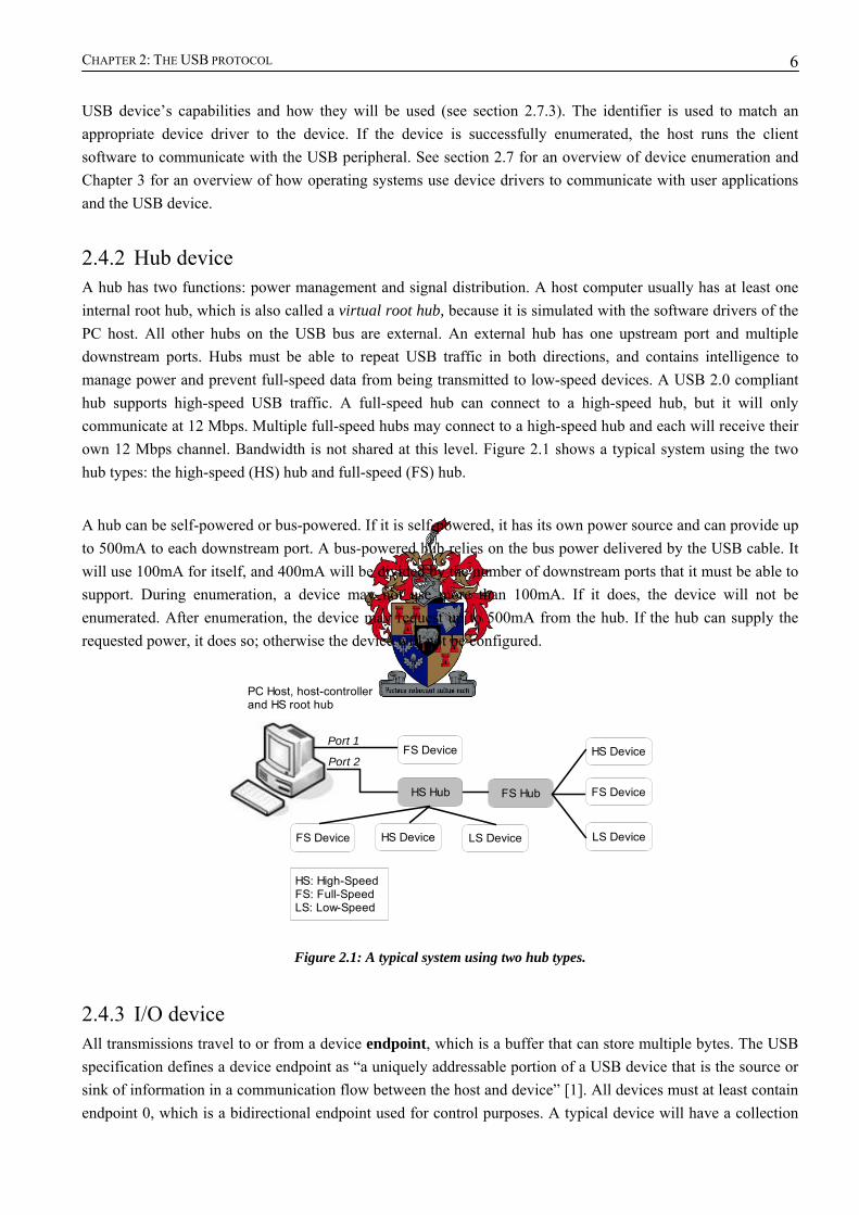
2.4.2 Hub device A hub has two functions: power management and signal distribution. A host computer usually has at least one internal root hub, which is also called a virtual root hub, because it is simulated with the software drivers of the PC host. All other hubs on the USB bus are external. An external hub has one upstream port and multiple downstream ports. Hubs must be able to repeat USB traffic in both directions, and contains intelligence to manage power and prevent full-speed data from being transmitted to low-speed devices. A USB 2.0 compliant hub supports high-speed USB traffic. A full-speed hub can connect to a high-speed hub, but it will only communicate at 12 Mbps. Multiple full-speed hubs may connect to a high-speed hub and each will receive their own 12 Mbps channel. Bandwidth is not shared at this level. Figure 2.1 shows a typical system using the two hub types: the high-speed (HS) hub and full-speed (FS) hub.
A hub can be self-powered or bus-powered. If it is self-powered, it has its own power source and can provide up to 500mA to each downstream port. A bus-powered hub relies on the bus power delivered by the USB cable. It will use 100mA for itself, and 400mA will be divided by the number of downstream ports that it must be able to support. During enumeration, a device may not use more than 100mA. If it does, the device will not be enumerated. After enumeration, the device may request up to 500mA from the hub. If the hub can supply the requested power, it does so; otherwise the device will not be configured.
FS Device
HS Hub
FS Device HS Device LS Device
FS Hub
HS Device
FS Device
LS Device
HS: High-SpeedFS: Full-SpeedLS: Low-Speed
Port 1
Port 2
PC Host, host-controllerand HS root hub
Figure 2.1: A typical system using two hub types.
2.4.3 I/O device All transmissions travel to or from a device endpoint, which is a buffer that can store multiple bytes. The USB specification defines a device endpoint as “a uniquely addressable portion of a USB device that is the source or sink of information in a communication flow between the host and device” [1]. All devices must at least contain endpoint 0, which is a bidirectional endpoint used for control purposes. A typical device will have a collection
CHAPTER 2: THE USB PROTOCOL
7
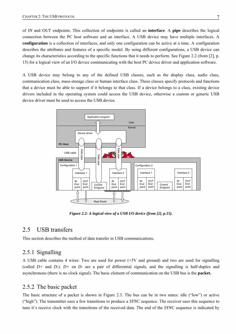
of IN and OUT endpoints. This collection of endpoints is called an interface. A pipe describes the logical connection between the PC host software and an interface. A USB device may have multiple interfaces. A configuration is a collection of interfaces, and only one configuration can be active at a time. A configuration describes the attributes and features of a specific model. By using different configurations, a USB device can change its characteristics according to the specific functions that it needs to perform. See Figure 2.2 (from [2], p. 15) for a logical view of an I/O device communicating with the host PC device driver and application software. A USB device may belong to any of the defined USB classes, such as the display class, audio class, communication class, mass-storage class or human interface class. These classes specify protocols and functions that a device must be able to support if it belongs to that class. If a device belongs to a class, existing device drivers included in the operating system could access the USB device, otherwise a custom or generic USB device driver must be used to access the USB device.
Interface 1
IN Endpoint
OUTEndpoint
Interface 2
IN Endpoint
OUTEndpoint
Control Endpoint
Configuration 1
Real World
Data pipe
Data pipe
Control pipe
Interface 1
IN Endpoint
OUTEndpoint
Interface 2
IN Endpoint
OUTEndpoint
Control Endpoint
Configuration 2
USB Device
USB cable
Application program
PC Host
Kernel
User
Device driver
Data pipe
Data pipe
Data pipe
Figure 2.2: A logical view of a USB I/O device (from [2], p.15).
2.5 USB transfers This section describes the method of data transfer in USB communications.
2.5.1 Signalling A USB cable contains 4 wires: Two are used for power (+5V and ground) and two are used for signalling (called D+ and D-). D+ en D- are a pair of differential signals, and the signalling is half-duplex and asynchronous (there is no clock signal). The basic element of communication on the USB bus is the packet.
2.5.2 The basic packet The basic structure of a packet is shown in Figure 2.3. The bus can be in two states: idle (“low”) or active (“high”). The transmitter uses a few transitions to produce a SYNC sequence. The receiver uses this sequence to tune it’s receive clock with the transitions of the received data. The end of the SYNC sequence is indicated by
CHAPTER 2: THE USB PROTOCOL
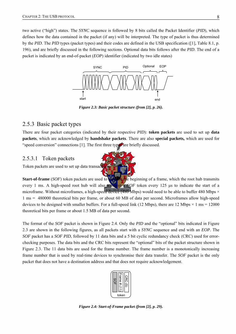
8
two active (“high”) states. The SYNC sequence is followed by 8 bits called the Packet Identifier (PID), which defines how the data contained in the packet (if any) will be interpreted. The type of packet is thus determined by the PID. The PID types (packet types) and their codes are defined in the USB specification ([1], Table 8.1, p. 196), and are briefly discussed in the following sections. Optional data bits follows after the PID. The end of a packet is indicated by an end-of-packet (EOP) identifier (indicated by two idle states)
Figure 2.3: Basic packet structure (from [2], p. 26).
2.5.3 Basic packet types There are four packet categories (indicated by their respective PID): token packets are used to set up data packets, which are acknowledged by handshake packets. There are also special packets, which are used for “speed conversion” connections [1]. The first three types are briefly discussed.
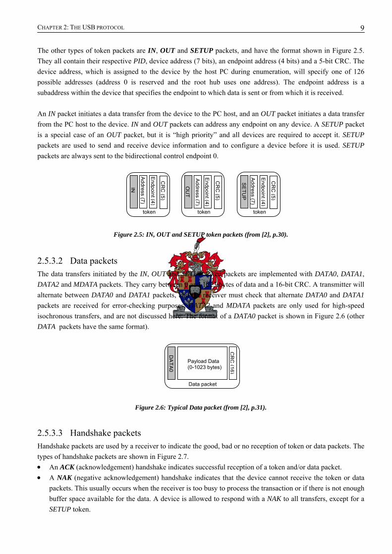
2.5.3.1 Token packets Token packets are used to set up data transactions. Start-of-frame (SOF) token packets are used to indicate the beginning of a frame, which the root hub transmits every 1 ms. A high-speed root hub will also transmit a SOF token every 125 μs to indicate the start of a microframe. Without microframes, a high-speed device (480 Mbps) would need to be able to buffer 480 Mbps × 1 ms = 480000 theoretical bits per frame, or about 60 MB of data per second. Microframes allow high-speed devices to be designed with smaller buffers. For a full-speed link (12 Mbps), there are 12 Mbps × 1 ms = 12000 theoretical bits per frame or about 1.5 MB of data per second. The format of the SOF packet is shown in Figure 2.4. Only the PID and the “optional” bits indicated in Figure 2.3 are shown in the following figures, as all packets start with a SYNC sequence and end with an EOP. The SOF packet has a SOF PID, followed by 11 data bits and a 5 bit cyclic redundancy check (CRC) used for error-checking purposes. The data bits and the CRC bits represent the “optional” bits of the packet structure shown in Figure 2.3. The 11 data bits are used for the frame number. The frame number is a monotonically increasing frame number that is used by real-time devices to synchronise their data transfer. The SOF packet is the only packet that does not have a destination address and that does not require acknowledgement.
Figure 2.4: Start-of-Frame packet (from [2], p. 29).
SO
F
Frame # (11)
CR
C (5)
token
SYNC PID Optional
start end
EOP
CHAPTER 2: THE USB PROTOCOL
9
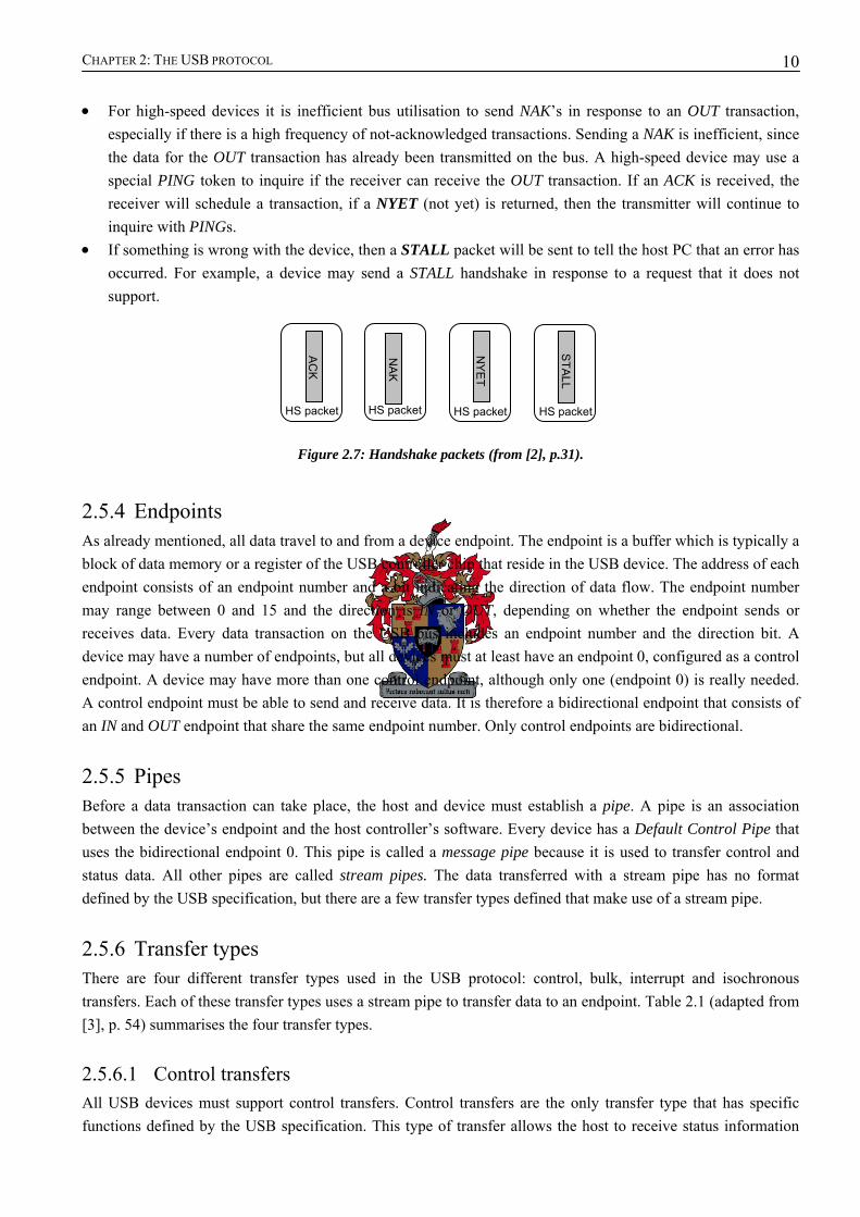
The other types of token packets are IN, OUT and SETUP packets, and have the format shown in Figure 2.5. They all contain their respective PID, device address (7 bits), an endpoint address (4 bits) and a 5-bit CRC. The device address, which is assigned to the device by the host PC during enumeration, will specify one of 126 possible addresses (address 0 is reserved and the root hub uses one address). The endpoint address is a subaddress within the device that specifies the endpoint to which data is sent or from which it is received. An IN packet initiates a data transfer from the device to the PC host, and an OUT packet initiates a data transfer from the PC host to the device. IN and OUT packets can address any endpoint on any device. A SETUP packet is a special case of an OUT packet, but it is “high priority” and all devices are required to accept it. SETUP packets are used to send and receive device information and to configure a device before it is used. SETUP packets are always sent to the bidirectional control endpoint 0.
Figure 2.5: IN, OUT and SETUP token packets (from [2], p.30).
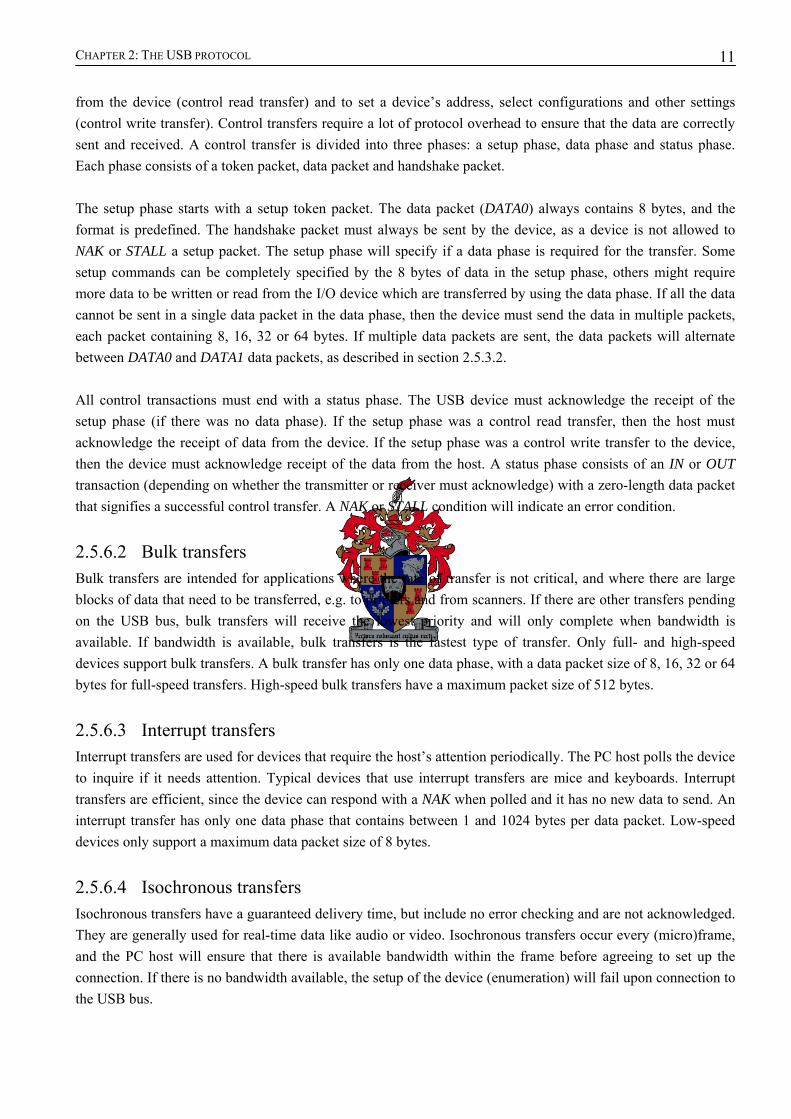
2.5.3.2 Data packets The data transfers initiated by the IN, OUT and SETUP token packets are implemented with DATA0, DATA1, DATA2 and MDATA packets. They carry between 0 and 1023 bytes of data and a 16-bit CRC. A transmitter will alternate between DATA0 and DATA1 packets, and the receiver must check that alternate DATA0 and DATA1 packets are received for error-checking purposes. DATA2 and MDATA packets are only used for high-speed isochronous transfers, and are not discussed here. The format of a DATA0 packet is shown in Figure 2.6 (other DATA packets have the same format).
Figure 2.6: Typical Data packet (from [2], p.31).
2.5.3.3 Handshake packets Handshake packets are used by a receiver to indicate the good, bad or no reception of token or data packets. The types of handshake packets are shown in Figure 2.7. • An ACK (acknowledgement) handshake indicates successful reception of a token and/or data packet. • A NAK (negative acknowledgement) handshake indicates that the device cannot receive the token or data
packets. This usually occurs when the receiver is too busy to process the transaction or if there is not enough buffer space available for the data. A device is allowed to respond with a NAK to all transfers, except for a SETUP token.
IN
Address (7)
Endpoint (4)
CR
C (5)
token O
UT
Address (7)
Endpoint (4)
CR
C (5)
token
SE
TUP
Address (7)
Endpoint (4)
CR
C (5)
token D
ATA
0
Payload Data (0-1023 bytes)
CR
C(16)
Data packet
CHAPTER 2: THE USB PROTOCOL
10
• For high-speed devices it is inefficient bus utilisation to send NAK’s in response to an OUT transaction, especially if there is a high frequency of not-acknowledged transactions. Sending a NAK is inefficient, since the data for the OUT transaction has already been transmitted on the bus. A high-speed device may use a special PING token to inquire if the receiver can receive the OUT transaction. If an ACK is received, the receiver will schedule a transaction, if a NYET (not yet) is returned, then the transmitter will continue to inquire with PINGs.
• If something is wrong with the device, then a STALL packet will be sent to tell the host PC that an error has occurred. For example, a device may send a STALL handshake in response to a request that it does not support.
Figure 2.7: Handshake packets (from [2], p.31).
2.5.4 Endpoints As already mentioned, all data travel to and from a device endpoint. The endpoint is a buffer which is typically a block of data memory or a register of the USB controller chip that reside in the USB device. The address of each endpoint consists of an endpoint number and a bit indicating the direction of data flow. The endpoint number may range between 0 and 15 and the direction is IN or OUT, depending on whether the endpoint sends or receives data. Every data transaction on the USB bus includes an endpoint number and the direction bit. A device may have a number of endpoints, but all devices must at least have an endpoint 0, configured as a control endpoint. A device may have more than one control endpoint, although only one (endpoint 0) is really needed. A control endpoint must be able to send and receive data. It is therefore a bidirectional endpoint that consists of an IN and OUT endpoint that share the same endpoint number. Only control endpoints are bidirectional.
2.5.5 Pipes Before a data transaction can take place, the host and device must establish a pipe. A pipe is an association between the device’s endpoint and the host controller’s software. Every device has a Default Control Pipe that uses the bidirectional endpoint 0. This pipe is called a message pipe because it is used to transfer control and status data. All other pipes are called stream pipes. The data transferred with a stream pipe has no format defined by the USB specification, but there are a few transfer types defined that make use of a stream pipe.
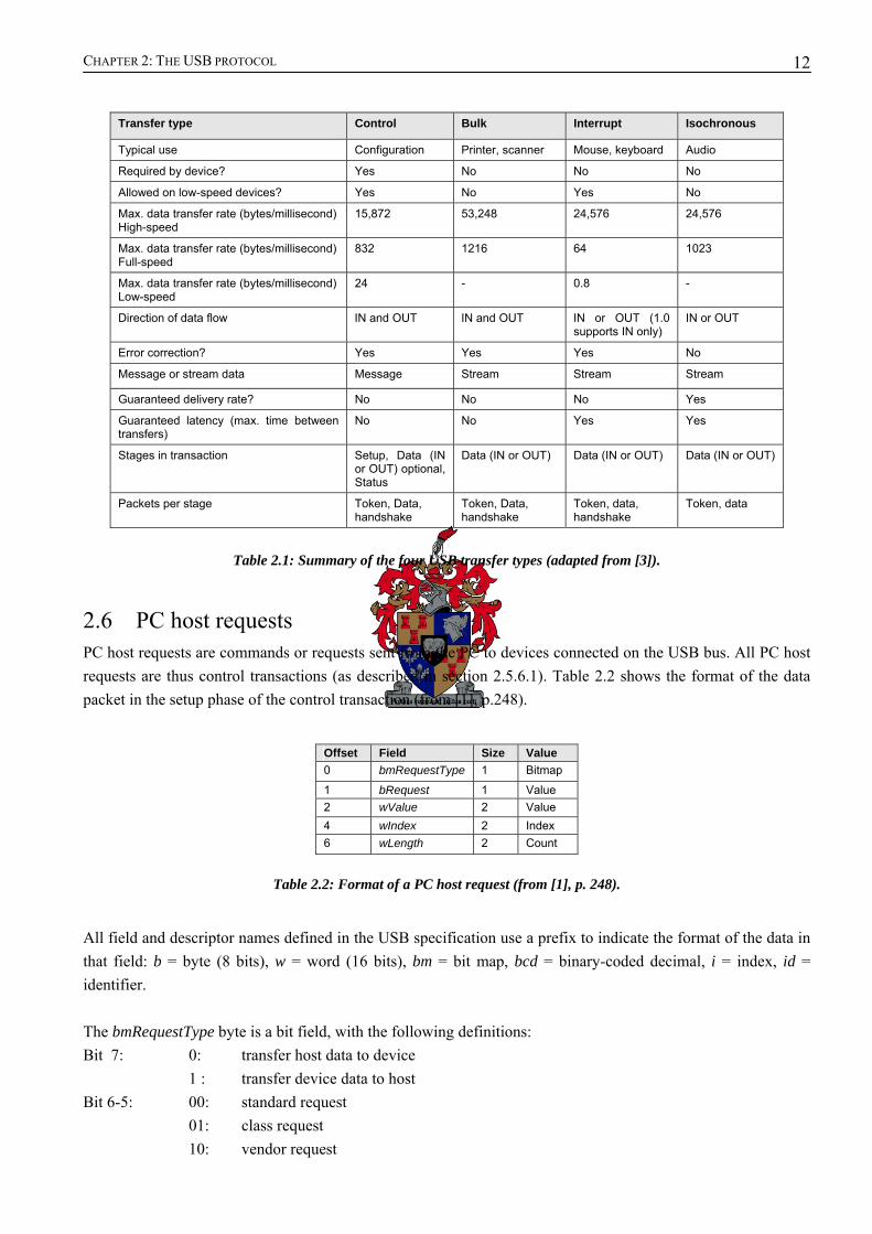
2.5.6 Transfer types There are four different transfer types used in the USB protocol: control, bulk, interrupt and isochronous transfers. Each of these transfer types uses a stream pipe to transfer data to an endpoint. Table 2.1 (adapted from [3], p. 54) summarises the four transfer types.
2.5.6.1 Control transfers All USB devices must support control transfers. Control transfers are the only transfer type that has specific functions defined by the USB specification. This type of transfer allows the host to receive status information
NA
K
AC
K
HS packet
NY
ET
STA
LL
HS packet HS packet HS packet
CHAPTER 2: THE USB PROTOCOL
11
from the device (control read transfer) and to set a device’s address, select configurations and other settings (control write transfer). Control transfers require a lot of protocol overhead to ensure that the data are correctly sent and received. A control transfer is divided into three phases: a setup phase, data phase and status phase. Each phase consists of a token packet, data packet and handshake packet. The setup phase starts with a setup token packet. The data packet (DATA0) always contains 8 bytes, and the format is predefined. The handshake packet must always be sent by the device, as a device is not allowed to NAK or STALL a setup packet. The setup phase will specify if a data phase is required for the transfer. Some setup commands can be completely specified by the 8 bytes of data in the setup phase, others might require more data to be written or read from the I/O device which are transferred by using the data phase. If all the data cannot be sent in a single data packet in the data phase, then the device must send the data in multiple packets, each packet containing 8, 16, 32 or 64 bytes. If multiple data packets are sent, the data packets will alternate between DATA0 and DATA1 data packets, as described in section 2.5.3.2. All control transactions must end with a status phase. The USB device must acknowledge the receipt of the setup phase (if there was no data phase). If the setup phase was a control read transfer, then the host must acknowledge the receipt of data from the device. If the setup phase was a control write transfer to the device, then the device must acknowledge receipt of the data from the host. A status phase consists of an IN or OUT transaction (depending on whether the transmitter or receiver must acknowledge) with a zero-length data packet that signifies a successful control transfer. A NAK or STALL condition will indicate an error condition.
2.5.6.2 Bulk transfers Bulk transfers are intended for applications where the rate of transfer is not critical, and where there are large blocks of data that need to be transferred, e.g. to printers and from scanners. If there are other transfers pending on the USB bus, bulk transfers will receive the lowest priority and will only complete when bandwidth is available. If bandwidth is available, bulk transfers is the fastest type of transfer. Only full- and high-speed devices support bulk transfers. A bulk transfer has only one data phase, with a data packet size of 8, 16, 32 or 64 bytes for full-speed transfers. High-speed bulk transfers have a maximum packet size of 512 bytes.
2.5.6.3 Interrupt transfers Interrupt transfers are used for devices that require the host’s attention periodically. The PC host polls the device to inquire if it needs attention. Typical devices that use interrupt transfers are mice and keyboards. Interrupt transfers are efficient, since the device can respond with a NAK when polled and it has no new data to send. An interrupt transfer has only one data phase that contains between 1 and 1024 bytes per data packet. Low-speed devices only support a maximum data packet size of 8 bytes.
2.5.6.4 Isochronous transfers Isochronous transfers have a guaranteed delivery time, but include no error checking and are not acknowledged. They are generally used for real-time data like audio or video. Isochronous transfers occur every (micro)frame, and the PC host will ensure that there is available bandwidth within the frame before agreeing to set up the connection. If there is no bandwidth available, the setup of the device (enumeration) will fail upon connection to the USB bus.
CHAPTER 2: THE USB PROTOCOL
12
Table 2.1: Summary of the four USB transfer types (adapted from [3]).
2.6 PC host requests PC host requests are commands or requests sent from the PC to devices connected on the USB bus. All PC host requests are thus control transactions (as described in section 2.5.6.1). Table 2.2 shows the format of the data packet in the setup phase of the control transaction (from [1], p.248).
Table 2.2: Format of a PC host request (from [1], p. 248).
All field and descriptor names defined in the USB specification use a prefix to indicate the format of the data in that field: b = byte (8 bits), w = word (16 bits), bm = bit map, bcd = binary-coded decimal, i = index, id = identifier. The bmRequestType byte is a bit field, with the following definitions: Bit 7: 0: transfer host data to device 1 : transfer device data to host Bit 6-5: 00: standard request 01: class request
10: vendor request
Transfer type Control Bulk Interrupt Isochronous
Typical use Configuration Printer, scanner Mouse, keyboard Audio
Required by device? Yes No No No
Allowed on low-speed devices? Yes No Yes No
Max. data transfer rate (bytes/millisecond) High-speed
15,872 53,248 24,576 24,576
Max. data transfer rate (bytes/millisecond) Full-speed
832 1216 64 1023
Max. data transfer rate (bytes/millisecond) Low-speed
24 - 0.8 -
Direction of data flow IN and OUT IN and OUT IN or OUT (1.0 supports IN only)
IN or OUT
Error correction? Yes Yes Yes No
Message or stream data Message Stream Stream Stream
Guaranteed delivery rate? No No No Yes
Guaranteed latency (max. time between transfers)
No No Yes Yes
Stages in transaction Setup, Data (IN or OUT) optional, Status
Data (IN or OUT) Data (IN or OUT) Data (IN or OUT)
Packets per stage Token, Data, handshake
Token, Data, handshake
Token, data, handshake
Token, data
Offset Field Size Value 0 bmRequestType 1 Bitmap
1 bRequest 1 Value 2 wValue 2 Value 4 wIndex 2 Index 6 wLength 2 Count
CHAPTER 2: THE USB PROTOCOL
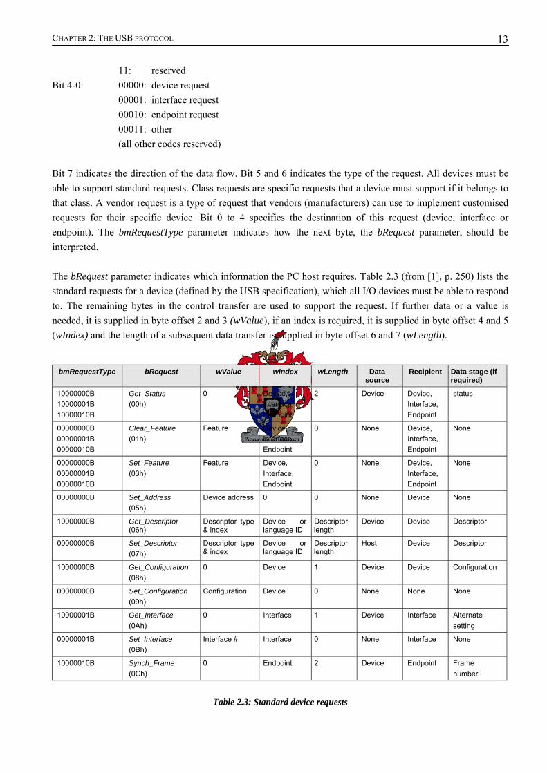
13
11: reserved Bit 4-0: 00000: device request 00001: interface request 00010: endpoint request 00011: other (all other codes reserved) Bit 7 indicates the direction of the data flow. Bit 5 and 6 indicates the type of the request. All devices must be able to support standard requests. Class requests are specific requests that a device must support if it belongs to that class. A vendor request is a type of request that vendors (manufacturers) can use to implement customised requests for their specific device. Bit 0 to 4 specifies the destination of this request (device, interface or endpoint). The bmRequestType parameter indicates how the next byte, the bRequest parameter, should be interpreted. The bRequest parameter indicates which information the PC host requires. Table 2.3 (from [1], p. 250) lists the standard requests for a device (defined by the USB specification), which all I/O devices must be able to respond to. The remaining bytes in the control transfer are used to support the request. If further data or a value is needed, it is supplied in byte offset 2 and 3 (wValue), if an index is required, it is supplied in byte offset 4 and 5 (wIndex) and the length of a subsequent data transfer is supplied in byte offset 6 and 7 (wLength).
Table 2.3: Standard device requests
bmRequestType bRequest wValue wIndex wLength Data source
Recipient Data stage (if required)
10000000B 10000001B 10000010B
Get_Status (00h)
0 Device, Interface, Endpoint
2 Device Device, Interface, Endpoint
status
00000000B 00000001B 00000010B
Clear_Feature (01h)
Feature
Device, Interface, Endpoint
0 None Device, Interface, Endpoint
None
00000000B 00000001B 00000010B
Set_Feature (03h)
Feature Device, Interface, Endpoint
0 None Device, Interface, Endpoint
None
00000000B Set_Address (05h)
Device address 0 0 None Device None
10000000B Get_Descriptor (06h)
Descriptor type & index
Device or language ID
Descriptor length
Device Device Descriptor
00000000B Set_Descriptor (07h)
Descriptor type & index
Device or language ID
Descriptor length
Host Device Descriptor
10000000B Get_Configuration (08h)
0 Device 1 Device Device Configuration
00000000B Set_Configuration (09h)
Configuration Device 0 None None None
10000001B Get_Interface (0Ah)
0 Interface 1 Device
Interface Alternate setting
00000001B Set_Interface (0Bh)
Interface # Interface 0 None Interface None
10000010B Synch_Frame (0Ch)
0 Endpoint 2 Device
Endpoint Frame number
CHAPTER 2: THE USB PROTOCOL
14
A summary of these standard requests are given below, but refer to the USB specification ([1], p. 250-260) for details. Get_Status: The host requests the status of the features of a device, interface or endpoint. The USB specification defines only two features: DEVICE_REMOTE_WAKEUP (01h) which applies to devices, or ENDPOINT_HALT (00h), which applies to endpoints. Clear_Feature: The host requests to disable a feature of a device, interface, or endpoint. When the host clears the DEVICE_REMOTE_WAKEUP feature, a suspended device cannot signal the host to resume communications. When the host clears the ENDPOINT_HALT feature, communication to and from an endpoint is resumed. An endpoint is halted when the PC host detected an error, e.g. if the endpoint buffer is empty when it is expected to contain data. Set_Feature: When the host sets the DEVICE_REMOTE_WAKEUP feature, a suspended device can signal the host to resume communications. When the host sets the ENDPOINT_HALT feature, communication to an endpoint is stopped, and can only be resumed using the “Clear_Feature” request. Set_Address: The host specifies an address to use in future communications with the device. This request is typically used during enumeration (refer to section 2.7). Get_Descriptor: The host requests a descriptor (descriptors are explained in section 2.7.3). Set_Descriptor: The host adds a descriptor or updates an existing descriptor. Get_Configuration: The host requests the value of the current device configuration. Set_Configuration: The host instructs the device to use the selected configuration. Get_Interface: For devices with configurations that support multiple settings for an interface, the host requests the current setting. Set_Interface: For devices with configurations that support multiple settings for an interface, the host requests the device to use a specific setting. Synch_Frame: The device sets and reports an endpoint’s synchronisation frame. In isochronous transfers, the communication between an endpoint and the host may vary in data packet size according to a specific sequence e.g. 8, 8, 8, 64 bytes. This request enables the host and endpoint to agree on which frame will begin the sequence.
2.7 Enumeration Before any communication can take place between the PC host and the USB device, the host needs to determine the device type and its capabilities so that it can assign a device driver. This initial communication is called enumeration.
CHAPTER 2: THE USB PROTOCOL
15
2.7.1 Device detection Inside the root hub, there are two biasing resistors connected to the D+ en D- signals of the USB bus. These resistors are connected to the ground voltage to ensure that D+ and D- are low when no device is connected to the bus. A USB device has resistors connected between either the D+ or D- signal of the USB bus and the positive supply voltage (Vcc). When a device is connected to the bus, the biasing resistors on the device’s side will cause D+ or D- to rise above ground voltage, and this change in voltage is recognised by the hub to detect the connection of a device. If the biasing resistor is connected to D+ , the device is informing the hub that it is a full-speed device, whereas a biasing resistor on D- indicates a low-speed device. A high-speed device is first detected as a full-speed device, and will later inform the root hub of its high-speed capabilities. After device detection, the PC host will initiate the enumeration process.
2.7.2 Enumeration steps 1. After the hub detected a newly attached device and determined its speed, the host controller requests the hub
to reset the port to which the device is connected. The hub places the device’s USB data lines in the reset condition (both data lines at logic low) for at least 10 milliseconds.
2. The host detects whether a full-speed device also supports high-speed. 3. The hub establishes a signal path between the device and the bus. The device is in its default state where it
will respond to control transfers over the default pipe at endpoint 0. The device can now communicate with the host, using the default address of 00h.
4. The host sends a Get_Descriptor request to determine the maximum packet size of the default pipe. The request is sent to device address 0, endpoint 0. The host enumerates only one device at a time, and only one device will thus respond to this request, even if several devices are attached at once. The device descriptor contains the maximum packet size supported by endpoint 0 (descriptors are discussed in section 2.7.3).
5. The host assigns a new unique address to the device using the Set_Address request. 6. The host learns about the device’s abilities using the Get_Descriptor request. The host continues to request
the different configuration descriptors specified in the device descriptor (see section 2.7.3). 7. The host assigns and loads a device driver. After the host determined the device’s properties from the device
descriptors, it assigns a matching device driver to the device. The device driver enables communication between the software applications and the hardware device. In selecting a driver, Microsoft Windows tries to match the information stored in the system’s .inf files with the vendor and product IDs retrieved from the device. The .inf files specifies which device driver should be used with which device.
8. The device driver selects a device configuration to use. The device driver requests a configuration by sending a Set_Configuration request to the device. The device is now ready for use.
2.7.3 Descriptor types During the enumeration process, the host PC requests descriptors from the device. Descriptors are data structures that contain information about the device’s configuration. All USB devices must be able to respond to requests for descriptors, therefore they must store these descriptors in memory and respond to requests for them in the expected format. The USB specification defines a hierarchy of descriptors ([1], p. 261), but not all of them are required. A device must contain at least one device descriptor. A device descriptor must contain at least one configuration descriptor, and a configuration descriptor must contain at least one interface descriptor (see Figure 2.8, p.17). If there are endpoints (other than control endpoint 0), the interface descriptor must contain descriptors for them as well. The most important descriptors are briefly explained in the following sections. Refer to the USB specification for more detailed explanations of the descriptors.
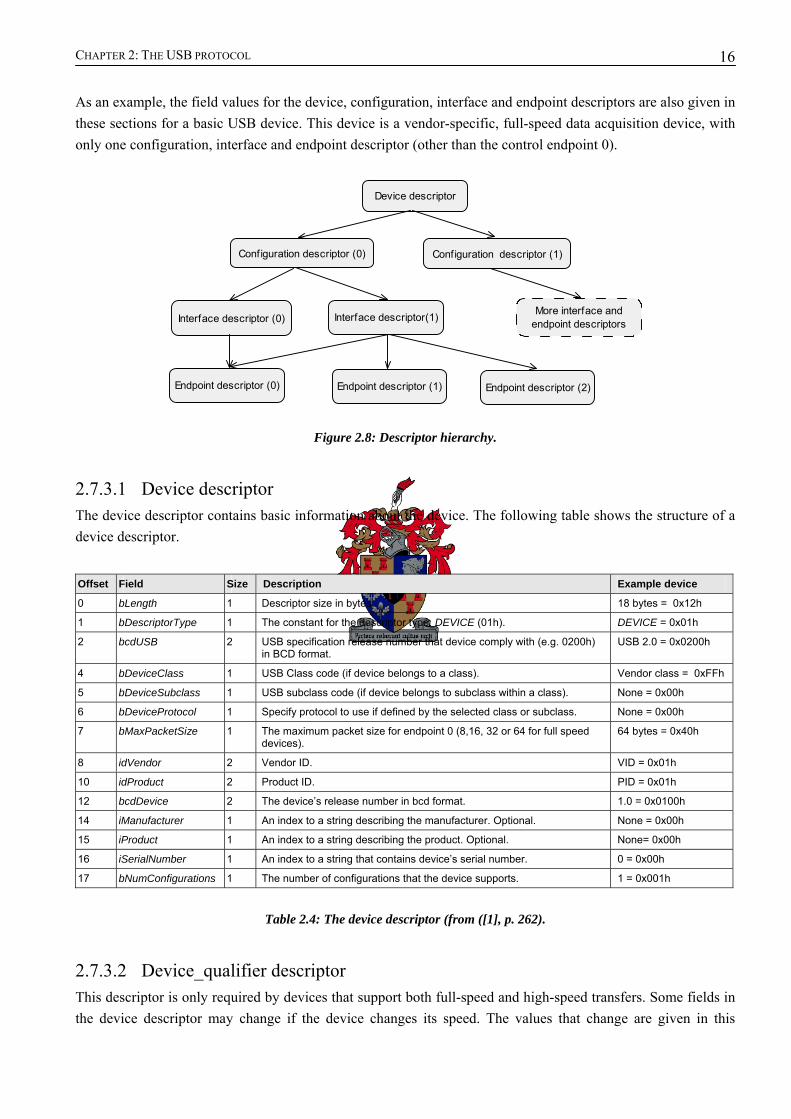
CHAPTER 2: THE USB PROTOCOL
16
As an example, the field values for the device, configuration, interface and endpoint descriptors are also given in these sections for a basic USB device. This device is a vendor-specific, full-speed data acquisition device, with only one configuration, interface and endpoint descriptor (other than the control endpoint 0).
Device descriptor
Configuration descriptor (0) Configuration descriptor (1)
Interface descriptor (0) Interface descriptor(1)
Endpoint descriptor (0) Endpoint descriptor (1)
More interface andendpoint descriptors
Endpoint descriptor (2)
Figure 2.8: Descriptor hierarchy.
2.7.3.1 Device descriptor The device descriptor contains basic information about the device. The following table shows the structure of a device descriptor.
Table 2.4: The device descriptor (from ([1], p. 262).
2.7.3.2 Device_qualifier descriptor This descriptor is only required by devices that support both full-speed and high-speed transfers. Some fields in the device descriptor may change if the device changes its speed. The values that change are given in this
Offset Field Size Description Example device
0 bLength 1 Descriptor size in bytes. 18 bytes = 0x12h
1 bDescriptorType 1 The constant for the descriptor type: DEVICE (01h). DEVICE = 0x01h
2 bcdUSB 2 USB specification release number that device comply with (e.g. 0200h) in BCD format.
USB 2.0 = 0x0200h
4 bDeviceClass 1 USB Class code (if device belongs to a class). Vendor class = 0xFFh
5 bDeviceSubclass 1 USB subclass code (if device belongs to subclass within a class). None = 0x00h
6 bDeviceProtocol 1 Specify protocol to use if defined by the selected class or subclass. None = 0x00h
7 bMaxPacketSize 1 The maximum packet size for endpoint 0 (8,16, 32 or 64 for full speed devices).
64 bytes = 0x40h
8 idVendor 2 Vendor ID. VID = 0x01h
10 idProduct 2 Product ID. PID = 0x01h
12 bcdDevice 2 The device’s release number in bcd format. 1.0 = 0x0100h
14 iManufacturer 1 An index to a string describing the manufacturer. Optional. None = 0x00h
15 iProduct 1 An index to a string describing the product. Optional. None= 0x00h
16 iSerialNumber 1 An index to a string that contains device’s serial number. 0 = 0x00h
17 bNumConfigurations 1 The number of configurations that the device supports. 1 = 0x001h
CHAPTER 2: THE USB PROTOCOL
17
descriptor and they swap values with the device descriptor when the device’s speed changes. The following table shows the structure of the device_qualifier descriptor.
Table 2.5: The device_qualifier descriptor (from [1], p. 264).
2.7.3.3 Configuration descriptor After the device descriptor is retrieved by the host, the device’s configuration, interface and endpoint descriptors are retrieved. Each device has at least one configuration descriptor, as shown in the following table. Often a single configuration is enough, but a device with multiple modes or uses can support multiple configurations. A data acquisition device, for example, may be configured to support multiple A/D (analogue to digital) channels at a lower speed or to support a single, high-speed A/D channel. Each configuration requires a descriptor. The configuration descriptor contains information about the device’s use of power and the number of interfaces that it supports.
Table 2.6: The configuration descriptor (from [1], p. 265).
2.7.3.4 Other_speed_configuration descriptor This descriptor is required by devices that support both full- and high-speed. It is the same as the configuration descriptor, but it describes the configuration when the device is operating at the speed that is not currently active.
Offset Field Size Description
0 bLength 1 Descriptor size in bytes.
1 bDescriptorType 1 The constant for the descriptor type: DEVICE_QUALIFIER (06h).
2 bcdUSB 2 USB specification release number that device comply with (e.g. 0200h) in bcd format.
4 bDeviceClass 1 USB Class code (if device belongs to a class).
5 bDeviceSubclass 1 USB subclass code (if device belongs to subclass within a class).
6 bDeviceProtocol 1 Specify protocol to use if defined by the selected class or subclass.
7 bMaxPacketSize 1 The maximum packet size for endpoint 0 (8,16, 32 or 64 for full speed devices).
8 Reserved 1 For future use.
Offset Field Size Description Example device
0 bLength 1 Descriptor size in bytes. 9 bytes = 0x09h
1 bDescriptorType 1 The constant for the descriptor type: CONFIGURATION (02h). CONFIG = 0x02h
2 wTotalLength 2 Size of all data returned for this configuration in bytes (total number of bytes contained in configuration, interface and endpoint descriptors).
26 bytes =0x1Ah
4 bNumInterfaces 1 Number of interfaces the configuration supports. 1 = 0x01h
5 bConfigurationValue 1 Identifier for Set_Configuration and Get_Configuration requests. 1 = 0x01h
6 iConfiguration 1 Index of string descriptor for this configuration. None = 0x00h
7 bmAttributes 1 Self power/bus power and remote wakeup settings. Bit 7=1, bit 6=1 if the device is self-powered, bit 5=1 if device supports remote wakeup feature, bit 4-0=0000 unused.
Bus powered, no remote wakeup 10000000b= 0x80h
8 MaxPower 1 Bus power required, expressed as (max. mA / 2). 300mA /2 = 0x96h
CHAPTER 2: THE USB PROTOCOL
18
Table 2.7: The other_speed_configuration descriptor (from [1], p. 267).
2.7.3.5 Interface descriptor The interface descriptor, shown in the following table, contains information about the endpoints that the interface supports. Each configuration must support at least one interface, but a configuration can have multiple interfaces that are active at the same time. Each interface has its own interface and endpoint descriptors. A device with multiple interfaces that are active at the same time is called a composite device and the host loads a driver for each interface. The host requests an alternate interface with the Set_Interface request, and reads the current interface number with the Get_Interface request.
Table 2.8: The interface descriptor (from [1], p. 268).
2.7.3.6 Endpoint descriptor Each endpoint specified in the interface descriptor must have a corresponding descriptor to describe its properties. Endpoint 0 does not have an endpoint descriptor because every device must support endpoint 0. Table 2.9 (p. 20) shows the structure of the endpoint descriptor.
2.7.3.7 String descriptor A string descriptor contains descriptive text about the manufacturer, product, serial number, configuration or interface. Each string has an index. String 0 has the special function of providing language ID’s (wLANGID), which are ID codes that indicate the languages that the strings are available in. String 1 and upwards may contain any text (bSTRING) that are encoded in Unicode. Unicode uses 16 bits to represent each character. Table 2.10 (p. 20) shows the structure of the string descriptor.
Offset Field Size Description
0 bLength 1 Descriptor size in bytes.
1 bDescriptorType 1 The constant for the descriptor type: OTHER_SPEED_CONFIGURATION (07h).
2 wTotalLength 2 Size of all data returned for this configuration in bytes.
4 bNumInterfaces 1 Number of interfaces the configuration supports.
5 bConfigurationValue 1 Identifier for Set_Configuration and Get_Configuration requests.
6 iConfiguration 1 Index of string descriptor for this configuration.
7 bmAttributes 1 Self power / bus power and remote wakeup settings. Bit 7 = 1, bit 6 = 1 if device is self-powered, bit 5 = 1 if device supports remote wakeup feature, bit 4-0 = 0000 unused.
8 MaxPower 1 Bus power required, expressed as (max. mA / 2).
Offset Field Size Description Example device
0 bLength 1 Descriptor size in bytes. 9 bytes = 0x09h
1 bDescriptorType 1 The constant for the descriptor type: INTERFACE (04h). INTERFACE = 0x04h
2 bInterfaceNumber 1 Number identifying this interface. 1 = 0x01h
3 bAlternateSetting 1 Value used to select an alternate setting. None = 0x00h
4 bNumEndpoints 1 Number of endpoints supported (excluding endpoint 0). 1 = 0x01h
5 iInterfaceClass 1 Class code for devices with a class specified by the interface. Vendor = 0xFFh
6 bInterfaceSubclass 1 Subclass code. Vendor = 0xFFh
7 bInterfaceProtocol 1 Protocol code. None = 0x00h
8 iInterface 1 Index of string descriptor for the interface. None = 0x00h
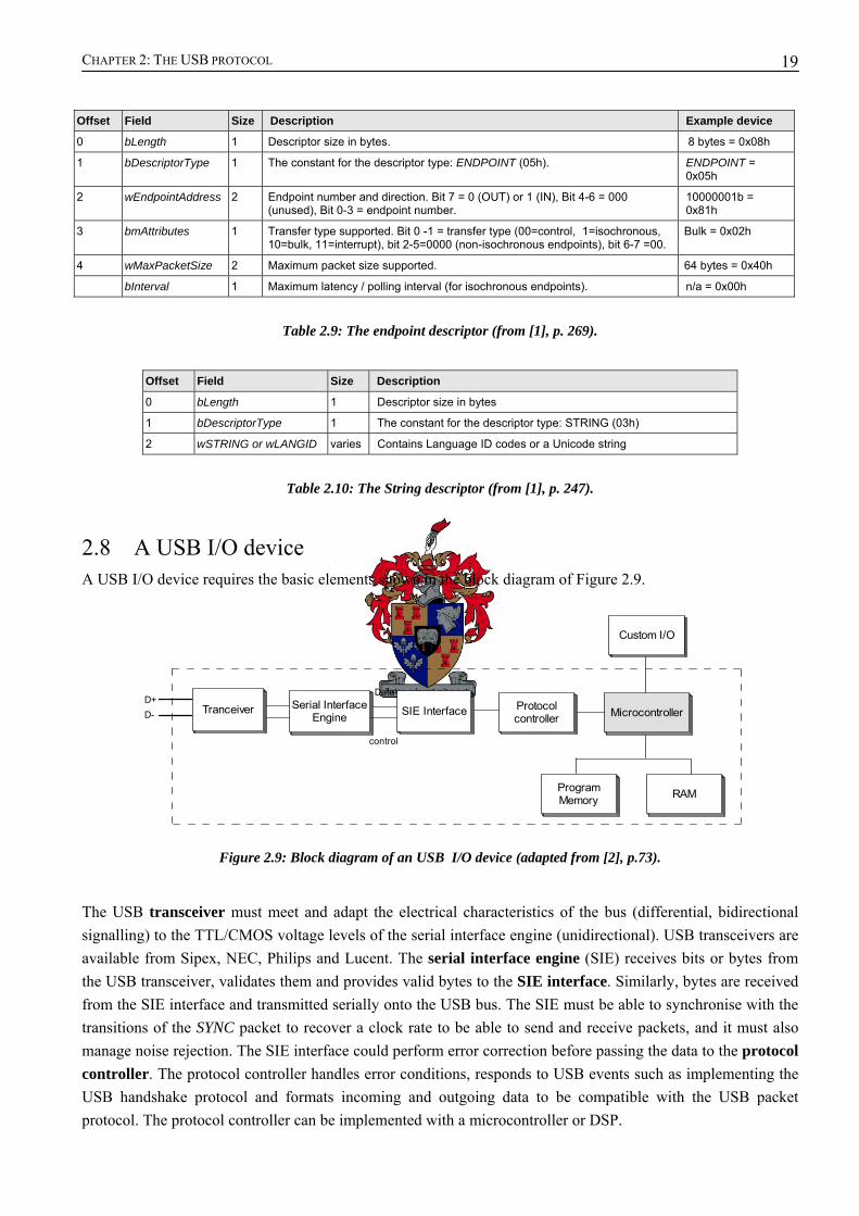
CHAPTER 2: THE USB PROTOCOL
19
Table 2.9: The endpoint descriptor (from [1], p. 269).
Offset Field Size Description
0 bLength 1 Descriptor size in bytes
1 bDescriptorType 1 The constant for the descriptor type: STRING (03h)
2 wSTRING or wLANGID varies Contains Language ID codes or a Unicode string
Table 2.10: The String descriptor (from [1], p. 247).
2.8 A USB I/O device A USB I/O device requires the basic elements shown in the block diagram of Figure 2.9.
Figure 2.9: Block diagram of an USB I/O device (adapted from [2], p.73).
The USB transceiver must meet and adapt the electrical characteristics of the bus (differential, bidirectional signalling) to the TTL/CMOS voltage levels of the serial interface engine (unidirectional). USB transceivers are available from Sipex, NEC, Philips and Lucent. The serial interface engine (SIE) receives bits or bytes from the USB transceiver, validates them and provides valid bytes to the SIE interface. Similarly, bytes are received from the SIE interface and transmitted serially onto the USB bus. The SIE must be able to synchronise with the transitions of the SYNC packet to recover a clock rate to be able to send and receive packets, and it must also manage noise rejection. The SIE interface could perform error correction before passing the data to the protocol controller. The protocol controller handles error conditions, responds to USB events such as implementing the USB handshake protocol and formats incoming and outgoing data to be compatible with the USB packet protocol. The protocol controller can be implemented with a microcontroller or DSP.
Offset Field Size Description Example device
0 bLength 1 Descriptor size in bytes. 8 bytes = 0x08h
1 bDescriptorType 1 The constant for the descriptor type: ENDPOINT (05h). ENDPOINT = 0x05h
2 wEndpointAddress 2 Endpoint number and direction. Bit 7 = 0 (OUT) or 1 (IN), Bit 4-6 = 000 (unused), Bit 0-3 = endpoint number.
10000001b = 0x81h
3 bmAttributes 1 Transfer type supported. Bit 0 -1 = transfer type (00=control, 1=isochronous, 10=bulk, 11=interrupt), bit 2-5=0000 (non-isochronous endpoints), bit 6-7 =00.
Bulk = 0x02h
4 wMaxPacketSize 2 Maximum packet size supported. 64 bytes = 0x40h
bInterval 1 Maximum latency / polling interval (for isochronous endpoints). n/a = 0x00h
Tranceiver Serial InterfaceEngine SIE Interface Protocol
controller Microcontroller
ProgramMemory RAM
Custom I/O
Data
control
D+D-

CHAPTER 2: THE USB PROTOCOL
20
Together these components handle all the USB communication functions, but to design a functional USB device one needs some input and output, together with a microcontroller, microprocessor or DSP to control these input and output signals. The microcontroller would most likely require some RAM and/or ROM to store temporary data and the program code that runs on the microcontroller (firmware). Fortunately, these components can be integrated and some vendors include them on a single chip, called an USB controller. There is a vast variety to choose from, all differing in architecture and complexity. USB controller chips vary in how much firmware support they require for USB communications. Some require the device’s program code to manage USB communications such as ensuring that the appropriate handshake packets and device descriptors are sent to the host. Others require little more than accessing a series of registers to store and retrieve USB data. Some controllers include a general-purpose CPU, while others interface to an external CPU to handle the non-USB tasks. Some controllers are designed from the ground up for USB applications. These are optimised for USB applications, instead of just adding USB functionality to an existing architecture. Those controllers that are based on existing architectures (like the very popular 8051) have the advantage that developers are already familiar with their architecture. All controller types include at least one USB port as well as buffers, registers and some I/O ports. A controller chip with a general-purpose CPU will also include on-chip program and data memory, or at least an interface to these as external components. One needs to study the specifications of these devices carefully, as they do not necessarily support all the transfer types and bus speeds, and some provide only a few endpoints. For high-volume applications that require fast performance, another option is to design and manufacture an application-specific integrated circuit (ASIC). The components for the design of these chips are available in synthesisable VHDL (very high speed integrated circuit hardware description language) or Verilog source code. Some companies derive their business by developing and supporting libraries of VHDL components. They are called SIP (semiconductor intellectual property) vendors. One can licence an entire USB controller design from a SIP vendor to add USB peripheral functionality to a FPGA design. For the purposes of this project, a controller that includes a general-purpose CPU and some on-chip RAM would be ideal. This would save development costs and time, and it would be an advantage if the chip is based on a familiar architecture, such as the 8051. In choosing a USB controller, there are some aspects to consider.
2.8.1 USB microcontroller selection criteria 1. The USB port: The USB controller must have an integrated USB transceiver and SIE. It must provide
buffers to retrieve data received from the USB bus and for storing data to be transmitted to the bus. Registers that are structured as FIFOs (first in, first out) would be ideal. The USB port should require very little firmware support for USB communications. This simplifies firmware design and allows the processor to perform other tasks.
2. The USB controller must support a number of endpoints. For this project, it is envisaged to have four telephony channels (at the most) that must be able to interface with the USB controller. It is thus required to have 4 IN endpoints (buffers to store telephony data to be sent to the PC host) and 4 OUT endpoints (buffers to store telephony data received from the PC host), as well as the required control endpoint 0.
3. Bus speed: The USB controller must be able to operate at the bus speed and support the transfer type required to send and receive telephony audio data. Generally, high- and full-speed controllers are more expensive. For this project we would, at most, have four telephony channels, each operating at 8 kHz with

CHAPTER 2: THE USB PROTOCOL
21
8-bit sampling. That translates to a maximum data rate of 256 Kbps if all four channels are used simultaneously. Control data would primarily be sent to and received from the telephony interface device when it is initialised, so that would not contribute to the steady-state data rate. The low-speed bus specification does not support bulk transfers, which would be required for this application. The full-speed specification supports all transfer types, and the bus speed would be sufficient for the required data rate. A USB controller for this project should thus support full-speed bus transfers.
4. The CPU: A CPU is required to transfer telephony data between the USB and the telephony circuit. The CPU must be based on a general-purpose microcontroller such as the 8051, which has a familiar architecture and instruction set.
5. Program memory: The USB controller must include storage for program memory. This could be EEPROM (electrically erasable programmable read-only memory) or RAM. EEPROM is a non-volatile type of memory, whereas RAM is volatile. During development it is likely that program memory will change often, therefore it is essential that it must be easy to change and store the program memory of the USB controller. Some chips are OTP (one-time programmable) and a new chip must be used if there are changes to the firmware. We require a USB controller that can be reprogrammed.
6. Data memory: The USB controller must have internal RAM, or at least access to external RAM for data memory. This project requires RAM to store telephony data that is transferred between the PC and the telephony interface.
7. Other I/O: The microcontroller must have general purpose input and output pins that can be used to interface to other circuits. The microcontroller must be able to send and receive control and data to telephony interfacing circuits. Some microcontrollers include built-in support for serial interfaces such as RS-232, I2C, microwire and SPI.
8. Other USB controller selection criteria include the ease of development, price and availability. Besides the abilities and features of the chip itself, ease of development is a major factor in how long it takes to get a project up and running. Some vendors have development boards available for their microcontroller which makes it easier to get started. A development board simplifies downloading and debugging of firmware. Detailed and well-organised documentation and sample firmware code are essential to start development with a microcontroller.
To save development time, the most firmware development is done in a high level language, like C, instead of assembly language which can be difficult to read and maintain. By using a language like C, the programmer does not have to be intimately familiar with the architecture of the microcontroller, and code developed in C will also be more portable to other systems than code developed in assembly. One must be sure that there is a compiler available that can compile the C code for the chosen chip architecture. If it is not available, the chip vendor must be able supply the compiler and tools that are needed to download the code to the USB controller’s program memory. Compilers for 8051-compatible chips are freely available, which is further motivation to choose a chip based on this architecture. Cypress, Infineon and Microchip are the most popular vendors that offer 8051-compatible, USB-capable microcontrollers. The Microchip PIC 16C7X5 series only have OTP program memory, which makes them unsuitable, while the USB microcontroller from Infineon requires a special “JTAG” programmer to download the firmware code. Cypress’ EZ-USB microcontroller family is notable because the chips support a different and flexible approach to storing firmware. Instead of storing the firmware on-chip in non-volatile memory, it stores the firmware on
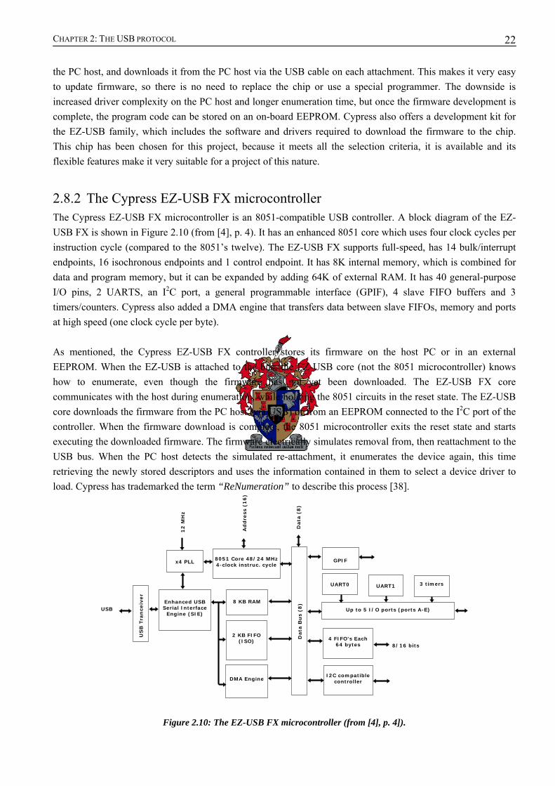
CHAPTER 2: THE USB PROTOCOL
22
the PC host, and downloads it from the PC host via the USB cable on each attachment. This makes it very easy to update firmware, so there is no need to replace the chip or use a special programmer. The downside is increased driver complexity on the PC host and longer enumeration time, but once the firmware development is complete, the program code can be stored on an on-board EEPROM. Cypress also offers a development kit for the EZ-USB family, which includes the software and drivers required to download the firmware to the chip. This chip has been chosen for this project, because it meets all the selection criteria, it is available and its flexible features make it very suitable for a project of this nature.
2.8.2 The Cypress EZ-USB FX microcontroller The Cypress EZ-USB FX microcontroller is an 8051-compatible USB controller. A block diagram of the EZ-USB FX is shown in Figure 2.10 (from [4], p. 4). It has an enhanced 8051 core which uses four clock cycles per instruction cycle (compared to the 8051’s twelve). The EZ-USB FX supports full-speed, has 14 bulk/interrupt endpoints, 16 isochronous endpoints and 1 control endpoint. It has 8K internal memory, which is combined for data and program memory, but it can be expanded by adding 64K of external RAM. It has 40 general-purpose I/O pins, 2 UARTS, an I2C port, a general programmable interface (GPIF), 4 slave FIFO buffers and 3 timers/counters. Cypress also added a DMA engine that transfers data between slave FIFOs, memory and ports at high speed (one clock cycle per byte). As mentioned, the Cypress EZ-USB FX controller stores its firmware on the host PC or in an external EEPROM. When the EZ-USB is attached to the bus, the EZ-USB core (not the 8051 microcontroller) knows how to enumerate, even though the firmware has not yet been downloaded. The EZ-USB FX core communicates with the host during enumeration, while holding the 8051 circuits in the reset state. The EZ-USB core downloads the firmware from the PC host (via USB) or from an EEPROM connected to the I2C port of the controller. When the firmware download is complete, the 8051 microcontroller exits the reset state and starts executing the downloaded firmware. The firmware electrically simulates removal from, then reattachment to the USB bus. When the PC host detects the simulated re-attachment, it enumerates the device again, this time retrieving the newly stored descriptors and uses the information contained in them to select a device driver to load. Cypress has trademarked the term “ReNumeration” to describe this process [38].
US
BTra
nce
iver
Enhanced USBSerial Interface
Engine (SIE)
8 KB RAM
2 KB FIFO(ISO)
DMA Engine
x4 PLL 8051 Core 48/24 MHz4-clock instruc. cycle
Data
Bu
s (8
)
GPIF
UART0 UART1 3 timers
4 FIFO's Each64 bytes
I2C compatiblecontroller
Up to 5 I/O ports (ports A-E)
8/16 bits
Data
(8
)
Ad
dre
ss (
16
)
12
MH
z
USB
Figure 2.10: The EZ-USB FX microcontroller (from [4], p. 4]).
CHAPTER 2: THE USB PROTOCOL
23
2.8.3 Firmware development environment Cypress included an evaluation version of Keil Corporation’s C compiler in the development kit. The evaluation version can only compile firmware programs up to 4 kilobytes (K), but the firmware for this project would most likely be larger than 4 K. To bypass this restriction, we can use a compiler called SDCC (Small Device C Compiler), which is an ANSI C compiler designed for 8051-based microprocessors. The entire source code for this compiler is distributed under GPL (GNU Public Licence). GPL is a licence created by the Free Software Foundation and provides for free software published under its terms (users are allowed to copy, modify and redistribute GPL software). The SDCC Compiler User Guide [5] is used as a reference. The compiler is very easy to use. It is a command line compiler that compiles and links the .c source file and creates .asm and .ihx output files. The .ihx file is a load module containing Intel hex records, which is downloaded to the microcontroller RAM. Cypress includes a software tool called “EZ-USB Control Panel” in the developer kit that has a function to download the firmware file to the microcontroller. Refer to Chapter 7 and 8 for the firmware design of the EZ-USB FX controller.

Chapter 3
3. The PC host software environment
The PC host software environment
3.1 Device drivers A device driver is a software component that enables applications to access a hardware device. A device driver insulates applications from requiring details about the physical connections, signals, protocols, addresses or ports the device attaches to. It translates between application-level and hardware-specific code. The application-level code uses functions supported by the operating system to communicate with the device, while the hardware-specific code handles the protocols necessary to access the peripheral’s circuits. A device driver can be a monolithic driver that handles everything from communicating with applications to reading and writing to the ports or memory addresses that connect to the device’s hardware. Other drivers use a layered driver model, where each driver in a series performs a portion of the communication between the application and the physical device. The top layer contains a function driver that manages communications between applications and the lower-level bus drivers. The bottom layer contains a bus driver that manages the communication between the function driver and the device. The layered driver model is more complicated as a whole, but it simplifies the task of writing a device driver, as many of the low-level hardware drivers may already exist, and only function drivers need to be written. It is also more efficient, because it enables different devices that have tasks in common to use the same driver for those tasks. For this project, the LibUSB driver will be used, which is a generic USB driver that allows user space application access to USB devices. To understand how this device driver works, one needs a basic understanding of how Microsoft Windows and Linux device drivers interface with application software and USB hardware.
3.2 Microsoft Windows driver environment The Microsoft Windows operating system uses the Win32 Driver Model (WDM) architecture to interface with USB devices. The Win32 Driver Model is a layered device driver architecture, shown in Figure 3.1. In Windows, code runs in either user mode or kernel mode. Applications must run in user mode and most drivers run in kernel mode. In user mode, Windows limits access to memory and other system resources, while in kernel mode, code has unrestricted access to system resources.

CHAPTER 3: THE PC HOST SOFTWARE ENVIRONMENT
25
Host controller driver (uhci.sys, openhci.sys)
Application
WIN32 subsystem
Filter driver
USB bus class driver (usbd.sys)
USB hub driver (usbhub.sys)
Class – function driver
USB hardware
User mode
Kernel mode
Function driver
Win 32 API calls
IRPs
IRPs
IRPs
IRPs
Bus drivers
Figure 3.1: The Win32 driver stack (adapted from [3], p.236).
The function driver enables applications to communicate with a USB device using a set of software functions, called an application programming interface (API). The API functions are part of Windows’ WDM subsystem. To communicate with a USB device, an application does not have to know anything about the USB protocol. The function driver knows how to communicate with the lower level device drivers. The kernel drivers communicate with each other using I/O Request Packets (IRPs). Windows includes class drivers for many standard device types (e.g. disk drives, printers etc.). If a USB device falls within a class specification and it has features or capabilities beyond what the class driver supports, a device-specific filter driver can support these as needed. Some devices are custom built and intended to be used only with a specific software application. These devices may use custom drivers, or they may be designed so that they comply with the specifications of a supported class. A custom driver would replace the function driver, but it would still need to fit into the layered architecture. The LibUSB driver (see section 3.4) is a custom driver. The USB bus driver consists of the root hub driver, the bus class driver and the host controller driver. The bus-class driver manages bus power, enumeration, USB transactions and the communications between the root hub driver and the host controller driver. The host controller driver enables the host controller hardware (which connects to the USB bus) to communicate with the upper USB drivers. The root hub driver manages the initialising of ports and manages communications between the function drivers and the bus class driver.
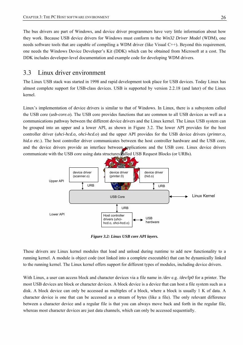
CHAPTER 3: THE PC HOST SOFTWARE ENVIRONMENT
26
device driver (scanner.o)
device driver (printer.0)
device driver (hid.o)
USB Core
Host controller drivers (uhci-hcd.o, ohci-hcd.o)
Upper API
Lower API
Linux Kernel
URB URB URB
URB
USB hardware
The bus drivers are part of Windows, and device driver programmers have very little information about how they work. Because USB device drivers for Windows must conform to the Win32 Driver Model (WDM), one needs software tools that are capable of compiling a WDM driver (like Visual C++). Beyond this requirement, one needs the Windows Device Developer’s Kit (DDK) which can be obtained from Microsoft at a cost. The DDK includes developer-level documentation and example code for developing WDM drivers.
3.3 Linux driver environment The Linux USB stack was started in 1998 and rapid development took place for USB devices. Today Linux has almost complete support for USB-class devices. USB is supported by version 2.2.18 (and later) of the Linux kernel. Linux’s implementation of device drivers is similar to that of Windows. In Linux, there is a subsystem called the USB core (usb-core.o). The USB core provides functions that are common to all USB devices as well as a communications pathway between the different device drivers and the Linux kernel. The Linux USB system can be grouped into an upper and a lower API, as shown in Figure 3.2. The lower API provides for the host controller driver (uhci-hcd.o, ohci-hcd.o) and the upper API provides for the USB device drivers (printer.o, hid.o etc.). The host controller driver communicates between the host controller hardware and the USB core, and the device drivers provide an interface between applications and the USB core. Linux device drivers communicate with the USB core using data structures called USB Request Blocks (or URBs).
Figure 3.2: Linux USB core API layers.
These drivers are Linux kernel modules that load and unload during runtime to add new functionality to a running kernel. A module is object code (not linked into a complete executable) that can be dynamically linked to the running kernel. The Linux kernel offers support for different types of modules, including device drivers. With Linux, a user can access block and character devices via a file name in /dev e.g. /dev/lp0 for a printer. The most USB devices are block or character devices. A block device is a device that can host a file system such as a disk. A block device can only be accessed as multiples of a block, where a block is usually 1 K of data. A character device is one that can be accessed as a stream of bytes (like a file). The only relevant difference between a character device and a regular file is that you can always move back and forth in the regular file, whereas most character devices are just data channels, which can only be accessed sequentially.
CHAPTER 3: THE PC HOST SOFTWARE ENVIRONMENT
27
A module implements one of these device types, and can thus be classified as a character module (character driver) or a block module (block driver). A character module implements the open, close, read and write system calls. A block driver offers the kernel the same interface as a character driver, as well as an additional block-oriented interface that is invisible to the user or applications opening the /dev files. A block interface, though, is essential to be able to mount a file system. Most USB device classes are supported in Linux. To write a custom driver, one needs basic knowledge of kernel compilation and some extensive programming experience in C under Linux.
3.4 LibUSB Since Windows and Linux implement their device drivers differently, the user space application interface to these drivers will differ as well. This is so, even if the device belongs to a class which both operating systems support. The API for the USB telephony interface device must be developed in such a way that it remains the same under both Windows and Linux development environments. LibUSB (http://libusb.sourceforge.net/) is a generic USB driver that that provides an API to user space applications to access USB devices, regardless of the operating system. It supports Linux, FreeBSD, NetBSD, OpenBSD, Darwin and MacOS. LibUSB-win32 (http://libusb-win32.sourceforge.net) is a ported version of LibUSB to the Windows operating systems (Win 98SE, Win ME, Win 2k, and Win XP). LibUSB-win32 is 100% API compatible with the main LibUSB project. It can be used as a filter driver for existing devices, or it can be used as a normal device driver for devices for which no driver exists (custom devices). The latest version (0.1.8) of LibUSB supports bulk, interrupt and control transfers. Unfortunately, isochronous transfers are not supported yet. This should not pose a problem, as the speed of bulk transfers should be sufficient for this project if we provide adequate buffering for incoming and outgoing telephony data. In this case, the only prerequisite would be that no other devices with a high bandwidth requirement may be connected on the same bus as the telephony interface device, as bulk transfers would receive the lowest priority. The following section briefly describes the LibUSB API (see [10] for details).
3.4.1 LibUSB functions
3.4.1.1 Core functions usb_init: Prototype: void usb_init(void);
Initialises the LibUSB internal structures for USB communication. This function must be called before any of the other LibUSB functions. The actual process initiated by this function is platform-specific. usb_find_busses: Prototype: int usb_find_busses(void);
Finds all busses on the system. It iterates through all of the USB resources and counts the number of changes on the bus (since the previous call to this function) and returns this number. If it is called for the first time, it will
CHAPTER 3: THE PC HOST SOFTWARE ENVIRONMENT
28
record all of the busses into a previously empty list of busses and return the total number of busses on the system. usb_find_devices: Prototype: int usb_find_devices(void);
Similar to usb_find_busses, but iterates through each bus to find the number of devices on each bus. Returns the number of changes since the previous call to this function. usb_get_busses: Prototype: struct usb_bus *usb_get_busses(void);
Returns the linked list of USB busses found. This was implemented for languages that support C calling conventions and that can use shared libraries, but do not support C global variables (like Delphi).
3.4.1.2 Device operations usb_open: Prototype: usb_dev_handle *usb_open(struct *usb_device dev);
Opens a USB device so that it can be used. It allocates memory for the data structures associated with an open USB device. This function must be called before attempting to perform any operations on the device. Returns a handle to be used in future communication with the device, or a null value on failure. usb_close: Prototype: int usb_close(usb_dev_handle *dev);
Closes a device opened with usb_open. It clears the data structures and releases control of the resources on the host computer. Without this function, it would be impossible to access the claimed USB hardware until the PC is rebooted. No further operations may be performed on the handle after usb_close is called. usb_set_configuration: Prototype: int usb_set_configuration(usb_dev_handle *dev, int configuration);
Sets the active configuration of a device. The configuration parameter is the value as specified in the descriptor field bConfigurationValue. Returns a 0 on success or an error value on failure. usb_set_altinterface: Prototype: int usb_set_altinterface(usb_dev_handle *dev,int alternate);
Sets the active alternate setting of the current interface. The alternate parameter is the value as specified in the descriptor field bAlternateSetting. Returns 0 on success or an error value on failure. usb_resetep: Prototype: int usb_resetep(usb_dev_handle *dev, unsigned int ep);
Resets the state of an endpoint specified by the ep parameter. Returns 0 on success or an error value on failure. usb_clear_halt: Prototype: int usb_clear_halt(usb_dev_handle *dev, unsigned int ep);
CHAPTER 3: THE PC HOST SOFTWARE ENVIRONMENT
29
Clears any halt status on an endpoint specified by the ep parameter. Returns 0 on success or a value (<0) on an error condition. usb_reset: Prototype: int usb_reset(usb_dev_handle *dev);
Resets a USB device. Any configuration that was made since it was opened will be lost, and the device will be forced to enumerate. Returns 0 on success or a value (<0) on an error condition. usb_claim_interface: Prototype: int usb_claim_interface(usb_dev_handle *dev, int interface);
Claims an interface of a device, specified by the interface parameter. This function must be called before any operations related to an interface are performed. The default interface can be claimed by using the descriptor field bInterfaceNumber. Returns 0 on success or a value (<0) on an error condition. usb_release_interface: Prototype: int usb_release_interface(usb_dev_handle *dev, int interface);
Releases a previously claimed interface, specified by the interface parameter. This function releases any previously claimed interface. Once this interface is released, a new interface must be claimed before any USB transfers can occur. Returns 0 on success or a value (<0) on an error condition.
3.4.1.3 Control transfers usb_control_msg: Prototype: int usb_control_msg(usb_dev_handle *dev, int bmRequestType, int
bRequest, int wValue, int wIndex, buffer *byte, int wLength, int
timeout);
Sends a control message (refer to section 2.6) to a device (using the default control pipe). The type of request is specified by the bRequestType parameter and the request itself by the bRequest parameter. The parameters wValue and wIndex corresponds to the arguments needed to support the request. The buffer parameter is a pointer to where the data is located, or where it is to be stored (depending on the type of request). The wLength parameter indicates the number of data bytes in the control transfer and timeout is the time after which the request will return with an error code (<0) if it is not processed. Returns 0 on success. usb_get_string: Prototype: int usb_get_string(usb_dev_handle *dev, int index, int langid, char
*buffer, int bLength);
Retrieves a string descriptor from device. The index parameter contains the index of the string, langid is the language ID of the string, buffer is the buffer where the string is to be stored and bLength is the size of this buffer. Returns 0 on success or a value (<0) on an error condition. usb_get_descriptor: Prototype: int usb_get_descriptor(usb_dev_handle *dev, unsigned char type,
unsigned char index, void *buffer, int buf_size);
CHAPTER 3: THE PC HOST SOFTWARE ENVIRONMENT
30
Retrieves a descriptor (via a device’s default control pipe), specified by the type and index parameters. The buffer parameter specifies where the descriptor is to be stored and bLength is the size of this buffer. Returns 0 on success or a value (<0) on an error condition.
usb_get_descriptor_by_endpoint: Prototype: int usb_get_descriptor_by_endpoint(usb_dev_handle *dev, int ep,
unsigned char type, unsigned char index, void *buf, int buf_size);
The same as usb_get_descriptor, but retrieves a descriptor via a control endpoint specified by ep, and not the default control endpoint 0. Returns 0 on success or a value (<0) on an error condition.
3.4.1.4 Bulk transfers usb_bulk_write: Prototype: int usb_bulk_write(usb_dev_handle *dev, int ep, buffer *bytes, int
length, int timeout);
Writes data to a bulk endpoint specified by ep. The data to be written is stored in buffer and the size of the buffer is specified by length. Returns 0 on success or a value (<0) on an error condition. The USB transfer will fail if it takes longer than timeout (milliseconds) to complete. usb_bulk_read: Prototype: int usb_bulk_read(usb_dev_handle *dev, int ep, buffer *bytes, int
length, int timeout);
Reads data from a bulk endpoint specified by parameter ep. The data is to be stored in buffer and the size of the buffer is specified by length. Returns 0 on success or a value (<0) on an error condition. The USB transfer will fail if it takes longer than timeout (milliseconds) to complete.
3.4.1.5 Interrupt transfers usb_interrupt_write: Prototype: int usb_interrupt_write(usb_dev_handle *dev, int ep, buffer *bytes,
int length, int timeout);
Writes data to an interrupt endpoint specified by parameter ep. The data to be written is stored in buffer and the size of the buffer is specified by length. Returns 0 on success or a value (<0) on an error condition. The USB transfer will fail if it takes longer than timeout (milliseconds) to complete. usb_interrupt_read: Prototype: int usb_interrupt_read(usb_dev_handle *dev, int ep, buffer *bytes,
int length, int timeout);
Reads data from an interrupt endpoint specified by parameter ep. The data is to be stored in buffer and the size of the buffer is specified by length. Returns 0 on success or a value (<0) on an error condition. The USB transfer will fail if it takes longer than timeout (milliseconds) to complete.
Chapter 4
4. The telephony interface
The telephony interface
The USB device must interface to the telephone network to be able to provide telephony access. The wireline telephone system is generally referred to as the public switched telephone network (PSTN), which is the total telephone network accessible by the public.
4.1 The telephone network The telephone network may implement different technologies, but for this project we are mainly interested in an analogue telephone connection. PSTN is a circuit-switched network, which means that the connection is only made for the duration of the telephone call. The connection between the customer premises equipment (CPE) and the central office (CO) is called the local loop. The central office (CO) connects the calling and called parties. The local loop usually consists of two twisted pairs of copper cable that runs between the central office and the customer premises. Only one pair is used, the other pair is for a second telephone line. The analogue loop between the CO and the customer premises is also referred to as a POTS (plain old telephone system). All computer telephony interfaces are connected either directly to the CO via the local loop or to a company PBX (Private Branch Exchange). A PBX connects to the CO with cables called trunks. A trunk is a digital or analogue connection between the PBX and the CO that allows a number of telephone conversations to occur simultaneously. All analogue and digital terminal equipment (TE) that connect to the telephone network must be compatible with the electrical and signalling requirements of the telephone network. The European Telecommunication Standards Institute (ETSI) and the International Telecommunication Union (ITU) are responsible for the setting of these standards used by telephony companies. Despite these standards however, analogue and digital telephony systems differ to some extent around the world. The South African telecommunication network, operated by Telkom, adheres to the ETSI and ITU specifications, and all equipment connecting to the network must be approved for use on the network.
4.1.1 Analogue vs. digital The analogue loop from the CO to the customer premises can be replaced with a digital line and digital equipment. The disadvantage of analogue telephony is that sound can be distorted or could carry an echo. Analogue lines also only transmit in the signal bandwidth from 300Hz to 3400Hz. Digital lines provide better sound quality, greater bandwidth and faster data transmission than analogue lines, but
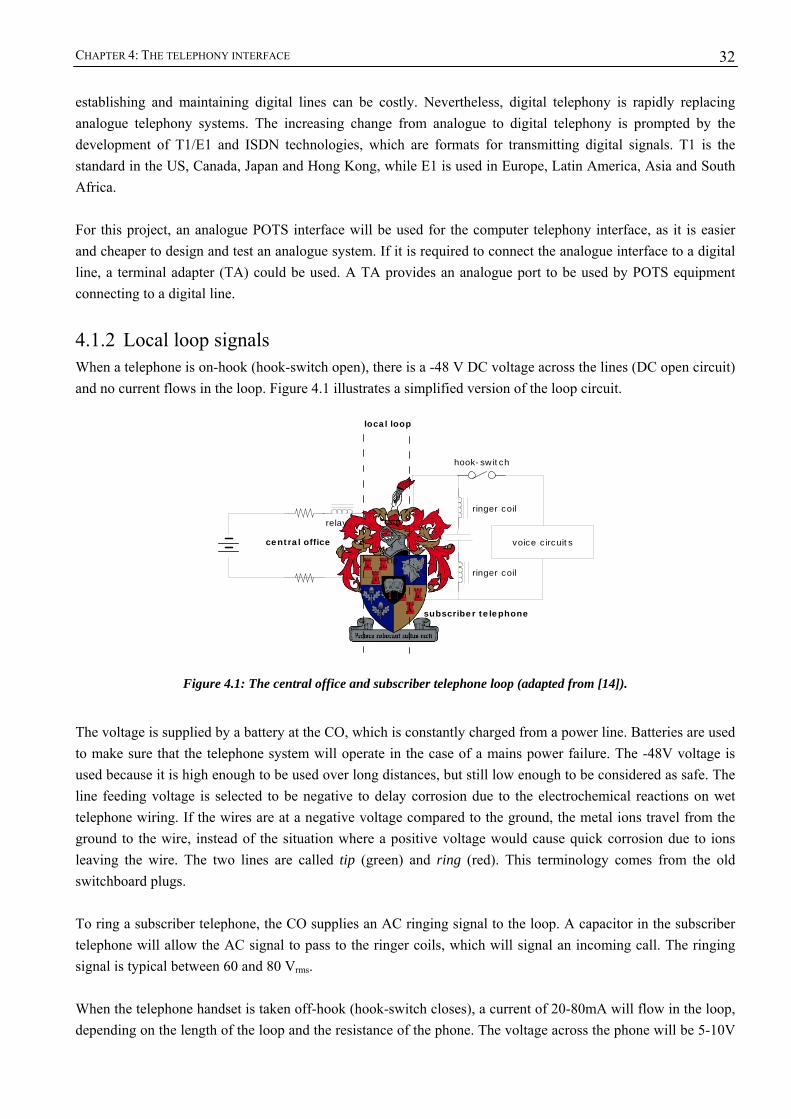
CHAPTER 4: THE TELEPHONY INTERFACE
32
establishing and maintaining digital lines can be costly. Nevertheless, digital telephony is rapidly replacing analogue telephony systems. The increasing change from analogue to digital telephony is prompted by the development of T1/E1 and ISDN technologies, which are formats for transmitting digital signals. T1 is the standard in the US, Canada, Japan and Hong Kong, while E1 is used in Europe, Latin America, Asia and South Africa. For this project, an analogue POTS interface will be used for the computer telephony interface, as it is easier and cheaper to design and test an analogue system. If it is required to connect the analogue interface to a digital line, a terminal adapter (TA) could be used. A TA provides an analogue port to be used by POTS equipment connecting to a digital line. 4.1.2 Local loop signals When a telephone is on-hook (hook-switch open), there is a -48 V DC voltage across the lines (DC open circuit) and no current flows in the loop. Figure 4.1 illustrates a simplified version of the loop circuit.
Figure 4.1: The central office and subscriber telephone loop (adapted from [14]).
The voltage is supplied by a battery at the CO, which is constantly charged from a power line. Batteries are used to make sure that the telephone system will operate in the case of a mains power failure. The -48V voltage is used because it is high enough to be used over long distances, but still low enough to be considered as safe. The line feeding voltage is selected to be negative to delay corrosion due to the electrochemical reactions on wet telephone wiring. If the wires are at a negative voltage compared to the ground, the metal ions travel from the ground to the wire, instead of the situation where a positive voltage would cause quick corrosion due to ions leaving the wire. The two lines are called tip (green) and ring (red). This terminology comes from the old switchboard plugs. To ring a subscriber telephone, the CO supplies an AC ringing signal to the loop. A capacitor in the subscriber telephone will allow the AC signal to pass to the ringer coils, which will signal an incoming call. The ringing signal is typical between 60 and 80 Vrms. When the telephone handset is taken off-hook (hook-switch closes), a current of 20-80mA will flow in the loop, depending on the length of the loop and the resistance of the phone. The voltage across the phone will be 5-10V
voice circuits
tip
ringrelay
central office
subscriber telephone
ringer coil
ringer coil
hook-switch
local loop
CHAPTER 4: THE TELEPHONY INTERFACE
33
and the rest will be dropped over the line resistance. When the hook-switch is closed, the voice circuits supply voice energy to the telephone line. To place a call, telephone systems use either the loop start or ground start method to initiate a call. In a loop start system, the telephone closes the hook-switch which creates a loop current. When the CO detects the loop current, it generates a dial tone and allows outward dialling. In a ground start system, one of the two telephone wires (tip or ring) is grounded. When the CO detects a ground wire, it generates a dial tone and allows outward dialling. Modern telephones use dual-tone multi-frequency (DTMF) tones to dial a number. In DTMF dialling, each key has two tones associated with it. The DTMF frequencies for each key (specified by ETSI) are shown in Table 4.1. The keys A to D are not found on a telephone keypad. They are DTMF frequencies used by military applications.
Table 4.1: DTMF frequencies.
The telephone network uses audible tones called progression tones to indicate the progress of a call. These tones include the dial tone, busy tone, hang-up tone and ringing tone. The different tones vary in frequency and cadence. Cadence is the alternating pattern of sound and silence, or on-time and off-time of the tone. Tones can either have one or two cycles, referred to as singe cycle or double cycle cadencies. The progression tones and cadencies are also specified by the ETSI and the ITU.
4.2 The POTS interface For this project, we need an interface circuit that would be able to connect the telephone network to the USB microcontroller. Pre-packaged circuits, called direct access arrangements (DAAs), are available and are used in modems, PBX systems and computer telephony applications. These are hybrid circuits or modules that contain many components in a single package. To find a suitable DAA, the requirements of a POTS interface for this project must be investigated.
4.2.1 Requirements • A complete DAA integrated solution is required, i.e. the circuit must interface to the telephone line and
provide a digital interface to the microcontroller. The DAA must require as few possible external components and the minimal analogue design. The digital interface must provide a data and control interface to the microcontroller.
• The DAA must include a hook-switch for breaking and closing the loop circuit. Traditionally, this is implemented using a hook-switch relay, but a transistor can also be used. It must provide control to put the device on- or off-hook.
• The DAA must have a hybrid network (2-to-4 wire converter). Since both transmit and receive signals are on the same telephone line pair at the same time (full-duplex), a mechanism is required such that the transmitted signal from the USB device is removed or minimised at the device’s receive path. The loss from the transmit path to receive path is known as the transhybrid loss, and it is desirable to have this loss as high
f(Hz) 1209 1336 1477 1633
697 1 2 3 A
770 4 5 6 B
852 7 8 9 C
941 * 0 # D

CHAPTER 4: THE TELEPHONY INTERFACE
34
as possible. Unfortunately, as voice signals are transmitted from the four-wire to the two-wire sections of the network, energy in the four-wire sections is reflected back (because of an impedance mismatch at the hybrid circuit), creating echoed speech. The actual amount of signal that is reflected back depends on how well the balance circuit of the hybrid matches the two-wire line. Additional echo cancellation circuitry in the echo path can reduce the echo.
• The DAA must provide the correct AC and DC termination required for the country’s telephone network. The DC termination determines the maximum loop current that will flow in off-hook conditions. If the loop current is too high, the DAA or PSTN equipment may be damaged. The AC termination must be selected to ensure that the maximum voice energy will be transmitted from the CO to the customer telephone. Improper impedance matching and termination can cause reflections that create noise and thus degrade the overall signal quality. Termination for telephone audio frequencies (300-3400 Hz) is typically specified to be 600Ω, but some counties, like South Africa, requires a complex AC termination impedance to satisfy the minimum return loss requirements. The hybrid circuit must be adjusted for each AC termination setting to achieve a maximum transhybrid loss.
• The interface must include a codec (coder/decoder), which is a device that encodes and decodes a signal. It is used to convert a digital signal to an analogue signal and vice versa. The analogue speech signal received from the telephone line must be converted to a digital format to be transmitted on the USB bus. A codec can also include compression and decompression technology. By discarding redundant data and reconstituting the signal on the receiving end, the amount of data to transmitted on the USB bus is reduced (conserving bandwidth). Section 4.2.2 presents an overview of voice digitisation and compression methods.
• The telephony interface must provide high-voltage isolation of the USB device circuitry from the telephone network. This is very important, as the voltages on the telephone network are very high in comparison with the voltages in the digital circuitry of the USB device. The analogue front end (AFE), which is the section of the circuit that interfaces to the telephone network, must be isolated from the rest of the telephony circuit (control circuitry and codec). It must be possible to separate the components in the PCB layout to form a high-voltage isolation barrier between the high-voltage circuitry (AFE) and the rest of the device circuitry. Traditionally, an isolation transformer is used to provide an isolated link between the high-and low-voltage circuitry, but capacitors and optocoupler-based techniques are also becoming popular.
• The DAA must provide surge and overvoltage protection, mostly for lightening induced transients, which could cause damage to equipment. The DAA must also include over-current protection that prevents the DAA from failing in such a way that it could compromise the isolation between the telephone network and the USB device circuitry.
• The DAA must have an incoming ring detector. • It must be possible to connect multiple DAAs in parallel to support multiple telephone channels. • The interface must meet ITU and ETSI specifications. The block diagram shown in Figure 4.2 shows the general components of a DAA required for this project.
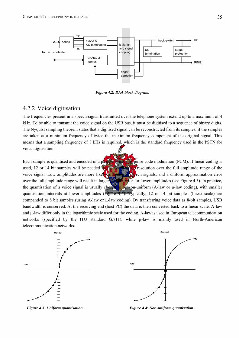
CHAPTER 4: THE TELEPHONY INTERFACE
35
To microcontroller
hybrid &AC termination
control &status
codec hook-switch
DCtermination
surgeprotection
TIP
RING
ringerdetection
isolationand signalcoupling
TX
RX
Figure 4.2: DAA block diagram.
4.2.2 Voice digitisation The frequencies present in a speech signal transmitted over the telephone system extend up to a maximum of 4 kHz. To be able to transmit the voice signal on the USB bus, it must be digitised to a sequence of binary digits. The Nyquist sampling theorem states that a digitised signal can be reconstructed from its samples, if the samples are taken at a minimum frequency of twice the maximum frequency component of the original signal. This means that a sampling frequency of 8 kHz is required, which is the standard frequency used in the PSTN for voice digitisation. Each sample is quantised and encoded in a process known as pulse code modulation (PCM). If linear coding is used, 12 or 14 bit samples will be needed to ensure adequate resolution over the full amplitude range of the voice signal. Low amplitudes are more likely in ordinary speech signals, and a uniform approximation error over the full amplitude range will result in larger relative error for lower amplitudes (see Figure 4.3). In practice, the quantisation of a voice signal is usually chosen to be non-uniform (A-law or μ-law coding), with smaller quantisation intervals at lower amplitudes (Figure 4.4). Typically, 12 or 14 bit samples (linear scale) are companded to 8 bit samples (using A-law or μ-law coding). By transferring voice data as 8-bit samples, USB bandwidth is conserved. At the receiving end (host PC) the data is then converted back to a linear scale. A-law and μ-law differ only in the logarithmic scale used for the coding. A-law is used in European telecommunication networks (specified by the ITU standard G.711), while μ-law is mainly used in North-American telecommunication networks. Figure 4.3: Uniform quantisation.
Figure 4.4: Non-uniform quantisation.
Output
Input
Output
Input
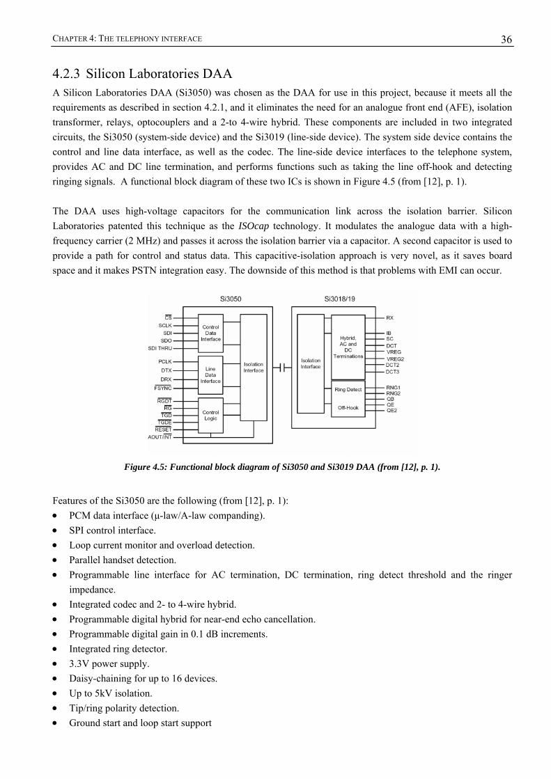
CHAPTER 4: THE TELEPHONY INTERFACE
36
4.2.3 Silicon Laboratories DAA A Silicon Laboratories DAA (Si3050) was chosen as the DAA for use in this project, because it meets all the requirements as described in section 4.2.1, and it eliminates the need for an analogue front end (AFE), isolation transformer, relays, optocouplers and a 2-to 4-wire hybrid. These components are included in two integrated circuits, the Si3050 (system-side device) and the Si3019 (line-side device). The system side device contains the control and line data interface, as well as the codec. The line-side device interfaces to the telephone system, provides AC and DC line termination, and performs functions such as taking the line off-hook and detecting ringing signals. A functional block diagram of these two ICs is shown in Figure 4.5 (from [12], p. 1). The DAA uses high-voltage capacitors for the communication link across the isolation barrier. Silicon Laboratories patented this technique as the ISOcap technology. It modulates the analogue data with a high-frequency carrier (2 MHz) and passes it across the isolation barrier via a capacitor. A second capacitor is used to provide a path for control and status data. This capacitive-isolation approach is very novel, as it saves board space and it makes PSTN integration easy. The downside of this method is that problems with EMI can occur.
Figure 4.5: Functional block diagram of Si3050 and Si3019 DAA (from [12], p. 1).
Features of the Si3050 are the following (from [12], p. 1): • PCM data interface (μ-law/A-law companding). • SPI control interface. • Loop current monitor and overload detection. • Parallel handset detection. • Programmable line interface for AC termination, DC termination, ring detect threshold and the ringer
impedance. • Integrated codec and 2- to 4-wire hybrid. • Programmable digital hybrid for near-end echo cancellation. • Programmable digital gain in 0.1 dB increments. • Integrated ring detector. • 3.3V power supply. • Daisy-chaining for up to 16 devices. • Up to 5kV isolation. • Tip/ring polarity detection. • Ground start and loop start support
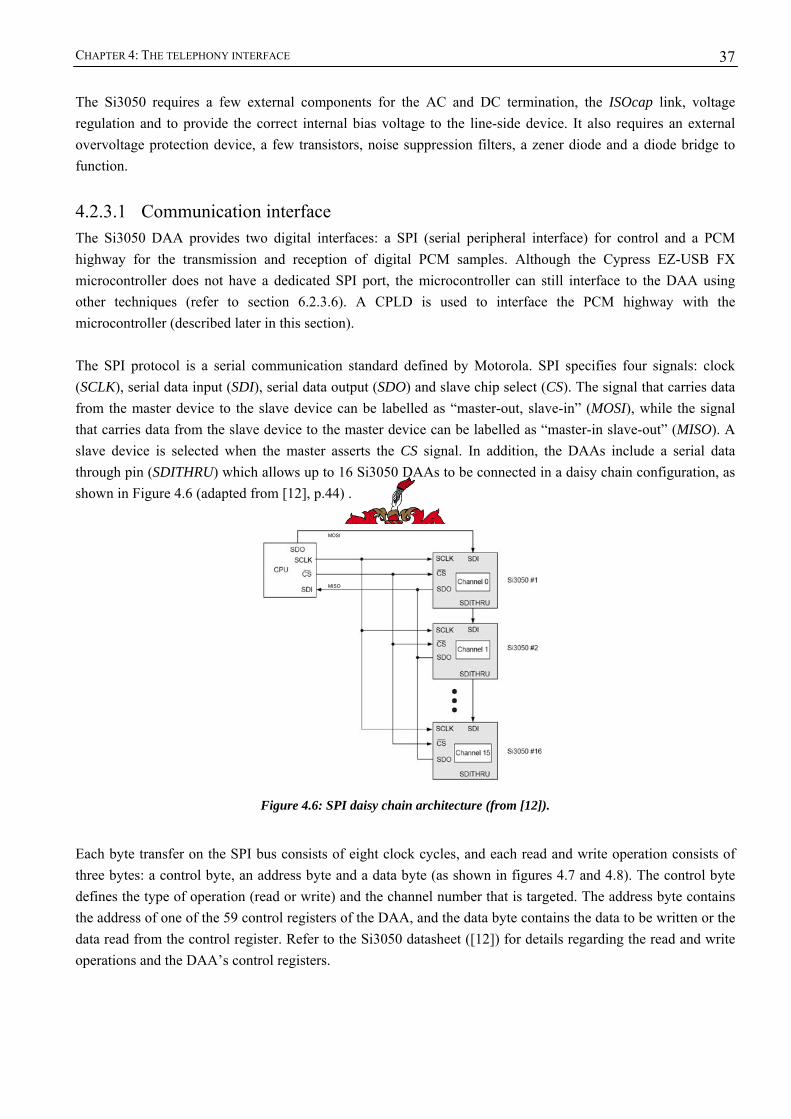
CHAPTER 4: THE TELEPHONY INTERFACE
37
The Si3050 requires a few external components for the AC and DC termination, the ISOcap link, voltage regulation and to provide the correct internal bias voltage to the line-side device. It also requires an external overvoltage protection device, a few transistors, noise suppression filters, a zener diode and a diode bridge to function.
4.2.3.1 Communication interface The Si3050 DAA provides two digital interfaces: a SPI (serial peripheral interface) for control and a PCM highway for the transmission and reception of digital PCM samples. Although the Cypress EZ-USB FX microcontroller does not have a dedicated SPI port, the microcontroller can still interface to the DAA using other techniques (refer to section 6.2.3.6). A CPLD is used to interface the PCM highway with the microcontroller (described later in this section). The SPI protocol is a serial communication standard defined by Motorola. SPI specifies four signals: clock (SCLK), serial data input (SDI), serial data output (SDO) and slave chip select (CS). The signal that carries data from the master device to the slave device can be labelled as “master-out, slave-in” (MOSI), while the signal that carries data from the slave device to the master device can be labelled as “master-in slave-out” (MISO). A slave device is selected when the master asserts the CS signal. In addition, the DAAs include a serial data through pin (SDITHRU) which allows up to 16 Si3050 DAAs to be connected in a daisy chain configuration, as shown in Figure 4.6 (adapted from [12], p.44) .
Figure 4.6: SPI daisy chain architecture (from [12]).
Each byte transfer on the SPI bus consists of eight clock cycles, and each read and write operation consists of three bytes: a control byte, an address byte and a data byte (as shown in figures 4.7 and 4.8). The control byte defines the type of operation (read or write) and the channel number that is targeted. The address byte contains the address of one of the 59 control registers of the DAA, and the data byte contains the data to be written or the data read from the control register. Refer to the Si3050 datasheet ([12]) for details regarding the read and write operations and the DAA’s control registers.
MISO
MOSI
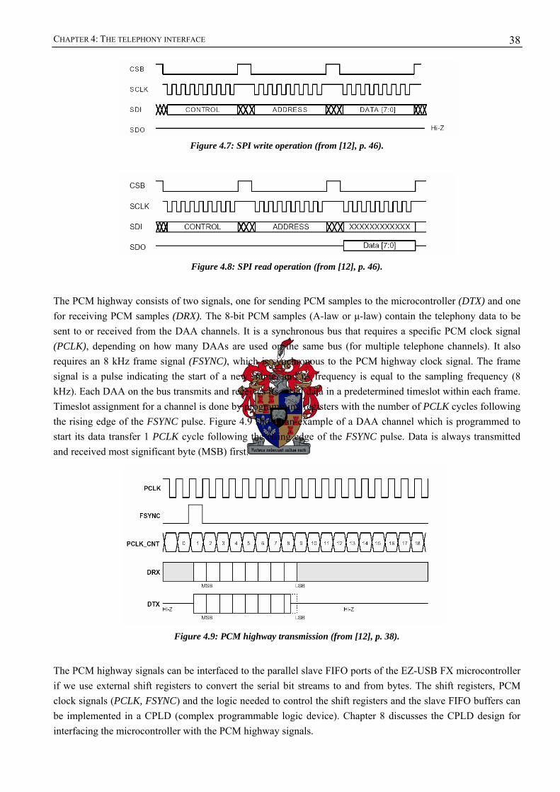
CHAPTER 4: THE TELEPHONY INTERFACE
38
Figure 4.7: SPI write operation (from [12], p. 46).
Figure 4.8: SPI read operation (from [12], p. 46).
The PCM highway consists of two signals, one for sending PCM samples to the microcontroller (DTX) and one for receiving PCM samples (DRX). The 8-bit PCM samples (A-law or μ-law) contain the telephony data to be sent to or received from the DAA channels. It is a synchronous bus that requires a specific PCM clock signal (PCLK), depending on how many DAAs are used on the same bus (for multiple telephone channels). It also requires an 8 kHz frame signal (FSYNC), which is synchronous to the PCM highway clock signal. The frame signal is a pulse indicating the start of a new frame, and its frequency is equal to the sampling frequency (8 kHz). Each DAA on the bus transmits and receives its serial data in a predetermined timeslot within each frame. Timeslot assignment for a channel is done by programming registers with the number of PCLK cycles following the rising edge of the FSYNC pulse. Figure 4.9 shows an example of a DAA channel which is programmed to start its data transfer 1 PCLK cycle following the rising edge of the FSYNC pulse. Data is always transmitted and received most significant byte (MSB) first.
Figure 4.9: PCM highway transmission (from [12], p. 38).
The PCM highway signals can be interfaced to the parallel slave FIFO ports of the EZ-USB FX microcontroller if we use external shift registers to convert the serial bit streams to and from bytes. The shift registers, PCM clock signals (PCLK, FSYNC) and the logic needed to control the shift registers and the slave FIFO buffers can be implemented in a CPLD (complex programmable logic device). Chapter 8 discusses the CPLD design for interfacing the microcontroller with the PCM highway signals.
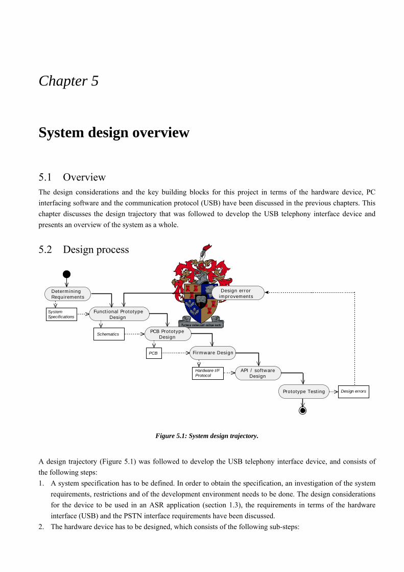
Chapter 5
5. System design overview
System design overview
5.1 Overview The design considerations and the key building blocks for this project in terms of the hardware device, PC interfacing software and the communication protocol (USB) have been discussed in the previous chapters. This chapter discusses the design trajectory that was followed to develop the USB telephony interface device and presents an overview of the system as a whole.
5.2 Design process
Functional Prototype Design
PCB Prototype Design
Firmware Design
API / software Design
Prototype Testing
SystemSpecifications
DeterminingRequirements
Schematics
PCB
Hardware I/FProtocol
Design error improvements
Design errors
Figure 5.1: System design trajectory.
A design trajectory (Figure 5.1) was followed to develop the USB telephony interface device, and consists of the following steps: 1. A system specification has to be defined. In order to obtain the specification, an investigation of the system
requirements, restrictions and of the development environment needs to be done. The design considerations for the device to be used in an ASR application (section 1.3), the requirements in terms of the hardware interface (USB) and the PSTN interface requirements have been discussed.
2. The hardware device has to be designed, which consists of the following sub-steps:
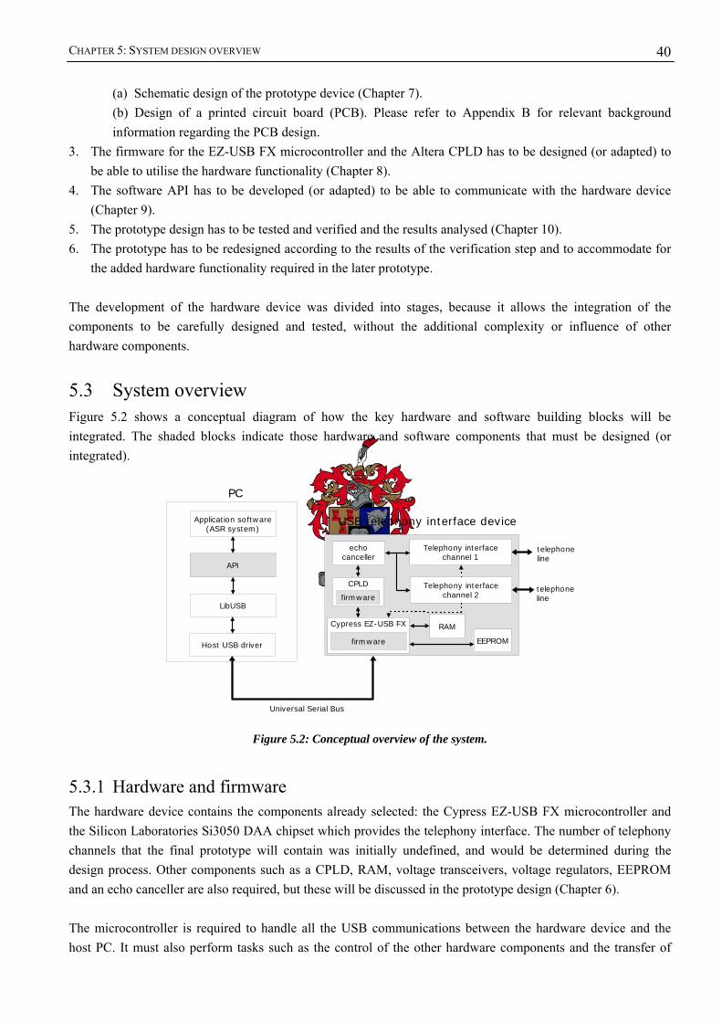
CHAPTER 5: SYSTEM DESIGN OVERVIEW
40
(a) Schematic design of the prototype device (Chapter 7). (b) Design of a printed circuit board (PCB). Please refer to Appendix B for relevant background information regarding the PCB design.
3. The firmware for the EZ-USB FX microcontroller and the Altera CPLD has to be designed (or adapted) to be able to utilise the hardware functionality (Chapter 8).
4. The software API has to be developed (or adapted) to be able to communicate with the hardware device (Chapter 9).
5. The prototype design has to be tested and verified and the results analysed (Chapter 10). 6. The prototype has to be redesigned according to the results of the verification step and to accommodate for
the added hardware functionality required in the later prototype. The development of the hardware device was divided into stages, because it allows the integration of the components to be carefully designed and tested, without the additional complexity or influence of other hardware components.
5.3 System overview Figure 5.2 shows a conceptual diagram of how the key hardware and software building blocks will be integrated. The shaded blocks indicate those hardware and software components that must be designed (or integrated).
Host USB driver
LibUSB
API
Application software(ASR system)
PC
USB telephony interface device
Cypress EZ-USB FX RAM
CPLD
Telephony interfacechannel 1
Telephony interfacechannel 2
Universal Serial Bus
telephoneline
telephonelinefirmware
firmware
echocanceller
EEPROM
Figure 5.2: Conceptual overview of the system.
5.3.1 Hardware and firmware The hardware device contains the components already selected: the Cypress EZ-USB FX microcontroller and the Silicon Laboratories Si3050 DAA chipset which provides the telephony interface. The number of telephony channels that the final prototype will contain was initially undefined, and would be determined during the design process. Other components such as a CPLD, RAM, voltage transceivers, voltage regulators, EEPROM and an echo canceller are also required, but these will be discussed in the prototype design (Chapter 6). The microcontroller is required to handle all the USB communications between the hardware device and the host PC. It must also perform tasks such as the control of the other hardware components and the transfer of
CHAPTER 5: SYSTEM DESIGN OVERVIEW
41
data between RAM and the USB endpoint buffers. The firmware required for the microcontroller to perform these tasks must be developed. As mentioned in section 4.2.3.1, a CPLD is required to implement the shift registers which interface between the microcontroller’s slave FIFO buffers and the PCM highway signals. The CPLD is also required for other purposes, such as generating the slave FIFO control logic, generating the PCM clock signals and to perform memory bank switching. The CPLD firmware must be developed.
5.3.2 Software The API which provides an interface to the USB telephony interface device must be developed. It must provide the necessary functions to make the telephony interface device suitable for use by ASR applications, as discussed in section 1.3. The API is written in ANSI C and may only use libraries that are platform-independent, such as LibUSB (refer to section 3.4) which provides the USB communications interface. This will allow the API to be compiled under both Microsoft Windows and Linux operating systems. The design of the API is discussed in Chapter 9.
Chapter 6
6. Prototype design
Prototype design
6.1 Overview The EZ-USB FX development board (CY3671) from Cypress was used to develop and test the first two prototype designs. The development board reduces development time, since all the hardware components and software drivers are already in place for a basic USB device to be attached to a PC and be enumerated. The development board allows firmware for the EZ-USB FX to be downloaded via the USB cable, which makes it easy to test and update the firmware for the device. The board also provides expansion and interfacing signals on 6 20-pin headers. This allows a mating prototype board to be attached to the development board during the construction and testing phase of a USB design. Finally, the development board contains components such as 128K of RAM, an in-circuit programmable CPLD and EPPROM that was used in the prototype designs, as well as other miscellaneous components (RS-232 level converters, I/O expander chips, seven-segment LED display etc.) that were not used. Two prototypes were designed using the development board, and are briefly discussed in this chapter. The hardware and firmware of the final stand-alone prototype design is discussed in detail in Chapters 7 and 8.
6.2 First prototype The first prototype design contained two DAA chipsets (for two telephone channels) and an Altera CPLD. The prototype was designed in the form of a mating board to be attached to the development board.
6.2.1 Hardware design The typical application circuit for the Si3050 ([12], p. 17) was used to design the DAA section of the circuit diagram. It specifies the components recommended by Silicon Laboratories for the external components required by the DAAs to operate correctly. A CPLD is required to interface between the PCM highway signals (from the DAAs) and the microcontroller’s slave FIFO buffers. An Altera CPLD was chosen, since the development software (MaxPlus II) and an in-circuit programmer was already available. One of the MAX 7000S family devices was chosen (EPM7160SLC), as this device meets the speed requirements needed for this project and was judged to have sufficient available resources (I/O pins and usable logic blocks). Section 6.2.2 describes the CPLD firmware design.
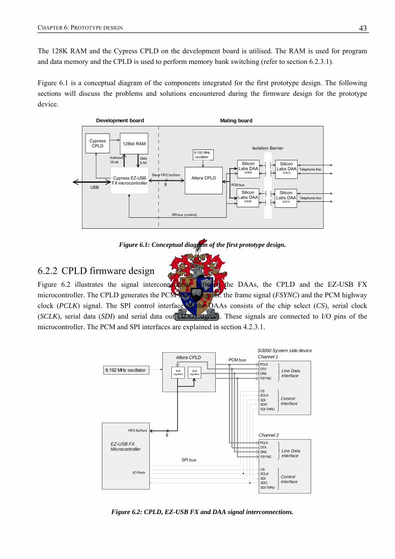
CHAPTER 6: PROTOTYPE DESIGN
43
The 128K RAM and the Cypress CPLD on the development board is utilised. The RAM is used for program and data memory and the CPLD is used to perform memory bank switching (refer to section 6.2.3.1). Figure 6.1 is a conceptual diagram of the components integrated for the first prototype design. The following sections will discuss the problems and solutions encountered during the firmware design for the prototype device.
Figure 6.1: Conceptual diagram of the first prototype design.
6.2.2 CPLD firmware design Figure 6.2 illustrates the signal interconnections between the DAAs, the CPLD and the EZ-USB FX microcontroller. The CPLD generates the PCM timing signals: the frame signal (FSYNC) and the PCM highway clock (PCLK) signal. The SPI control interface of the DAAs consists of the chip select (CS), serial clock (SCLK), serial data (SDI) and serial data out (SDO) signals. These signals are connected to I/O pins of the microcontroller. The PCM and SPI interfaces are explained in section 4.2.3.1.
Figure 6.2: CPLD, EZ-USB FX and DAA signal interconnections.
Cypress EZ-USBFX microcontroller
CypressCPLD 128kb RAM
Address16-bit
Data8-bit
USB
Development board
Slave FIFO buffersAltera CPLD
SiliconLabs DAA
Si3050
SiliconLabs DAA
Si3050
SiliconLabs DAA
Si3019
SiliconLabs DAA
Si3019
Telephone line
Telephone line
PCM bus
8.192 MHzoscillator
SPI bus (control)
Mating board
Isolation Barrier
//8
PCLKDTXDRXFSYNC
CSSCLKSDISDOSDI THRU
Line Datainterface
Controlinterface
Si3050 System side deviceChannel 1
PCLKDTXDRXFSYNC
CSSCLKSDISDOSDI THRU
Line Datainterface
Controlinterface
Channel 2
Shiftregisters
Altera CPLD
EZ-USB FXMicrocontroller
FIFO Buffers
I/O Ports
8.192 MHz oscillator
//8
SPI bus
PCM bus
Shiftregisters
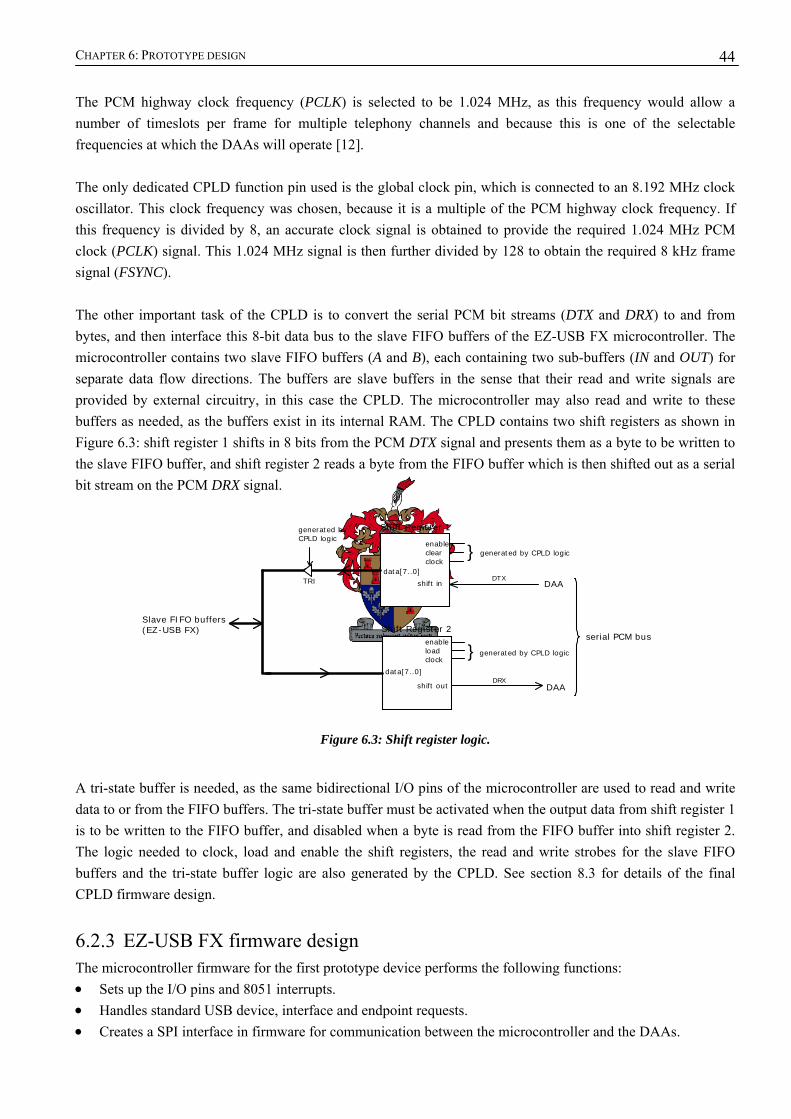
CHAPTER 6: PROTOTYPE DESIGN
44
The PCM highway clock frequency (PCLK) is selected to be 1.024 MHz, as this frequency would allow a number of timeslots per frame for multiple telephony channels and because this is one of the selectable frequencies at which the DAAs will operate [12]. The only dedicated CPLD function pin used is the global clock pin, which is connected to an 8.192 MHz clock oscillator. This clock frequency was chosen, because it is a multiple of the PCM highway clock frequency. If this frequency is divided by 8, an accurate clock signal is obtained to provide the required 1.024 MHz PCM clock (PCLK) signal. This 1.024 MHz signal is then further divided by 128 to obtain the required 8 kHz frame signal (FSYNC). The other important task of the CPLD is to convert the serial PCM bit streams (DTX and DRX) to and from bytes, and then interface this 8-bit data bus to the slave FIFO buffers of the EZ-USB FX microcontroller. The microcontroller contains two slave FIFO buffers (A and B), each containing two sub-buffers (IN and OUT) for separate data flow directions. The buffers are slave buffers in the sense that their read and write signals are provided by external circuitry, in this case the CPLD. The microcontroller may also read and write to these buffers as needed, as the buffers exist in its internal RAM. The CPLD contains two shift registers as shown in Figure 6.3: shift register 1 shifts in 8 bits from the PCM DTX signal and presents them as a byte to be written to the slave FIFO buffer, and shift register 2 reads a byte from the FIFO buffer which is then shifted out as a serial bit stream on the PCM DRX signal.
Figure 6.3: Shift register logic.
A tri-state buffer is needed, as the same bidirectional I/O pins of the microcontroller are used to read and write data to or from the FIFO buffers. The tri-state buffer must be activated when the output data from shift register 1 is to be written to the FIFO buffer, and disabled when a byte is read from the FIFO buffer into shift register 2. The logic needed to clock, load and enable the shift registers, the read and write strobes for the slave FIFO buffers and the tri-state buffer logic are also generated by the CPLD. See section 8.3 for details of the final CPLD firmware design.
6.2.3 EZ-USB FX firmware design The microcontroller firmware for the first prototype device performs the following functions: • Sets up the I/O pins and 8051 interrupts. • Handles standard USB device, interface and endpoint requests. • Creates a SPI interface in firmware for communication between the microcontroller and the DAAs.
data[7..0]
shift out
enableloadclock
data[7..0]
shift in
enableclearclock
Shift Register 1
Shift Register 2
DRX
DTXTRI
Slave FIFO buffers(EZ-USB FX)
serial PCM bus
DAA
DAA
generated byCPLD logic
generated by CPLD logic
generated by CPLD logic
CHAPTER 6: PROTOTYPE DESIGN
45
• Initialises the DAAs. • Handles requests from the host PC, such as requesting size of buffers, requesting status of a channel,
answering calls, hanging up calls etc. • Detects if a DAA is connected to a telephone line, if a ringing signal is detected or if it is off-hook. • Transfers data between the FIFO buffers, RAM and endpoint buffers.
6.2.3.1 Memory issues The 8051 microcontroller has a modified Harvard architecture with separate address spaces for program and data memory (although it has only one address and data bus). It can address 64K of external data memory and 64K of external program memory, which may be two separate blocks of memory. The microcontroller generates two read signals, RD# and PSEN#. The first signal (RD#) is used to read from the external data memory while PSEN# is used to read from external program memory. The two read signals may be combined with a logic AND operation so that the same block of memory is mapped to act as both program and data memory. This is referred to as the Von Neumann architecture1. In this project, it is preferred to use the Harvard architecture as the microcontroller’s memory capacity is doubled and it is easier to use separate blocks of RAM for program and data memory. It is, however, an awkward architecture to use with the EZ-USB FX microcontroller, because firmware needs to be loaded into external program memory during enumeration. The microcontroller has 8K of internal RAM available for program memory, which is insufficient space for a project of this scale. Also, during enumeration the USB core can only write downloaded firmware code to the internal memory of the microcontroller (section 2.8.2). By adopting the Von Neumann architecture, firmware code may be written to external memory as data bytes, and then executed as program instructions. To implement this, a second-stage boot loader, which is capable of writing firmware code to external RAM, is required (discussed in section 6.2.3.2). The development board’s CPLD, which controls the memory access, was reprogrammed so that it is possible for the microcontroller to switch between using the Harvard or the Von Neumann architecture. The CPLD Verilog source code, developed by Cypress ([15], p. 4-17), was adapted for this purpose. To program the Cypress development board CPLD, an “UltraISR” programming cable is required [20]. A programming cable, based on a HC244 CMOS buffer chip ([20], p. 4, Figure 3), was built and used to reprogram the Cypress CPLD. A control signal between the microcontroller and the CPLD selects the memory architecture to use. When the Harvard architecture is selected, the CPLD will use the first 64K bank of the 128K RAM on the development board for the program memory and the second 64K bank will be used for data memory. When the Von Neumann architecture is selected, the first 64K bank is used for both program and data memory. This architecture is only selected when the boot loader is running on the microcontroller, as it is required to write firmware code to external program memory as data bytes. The addresses between 0x7800 and 0x7FFF are used for bulk endpoint buffers of the EZ-USB FX, and are also mapped to the region 0x1B40-0x1FFF in internal RAM to remain compatible with a previous version of the microcontroller that had the buffers mapped to this area. These areas may not be used for program or data memory. Figure 6.4 illustrates the internal RAM usage of the EZ-USB FX.
1 Named after John Von Neumann, a mathematician and computer scientist of the 20th century.
CHAPTER 6: PROTOTYPE DESIGN
46
Data/ Code RAM(6976 bytes)
0x000
0x1B3F
0x1FFF
0x7800
0x7FFF
Bulk endpoint buffers
Bulk endpoint buffers
8K internal RAM
Figure 6.4: Internal RAM usage.
6.2.3.2 Boot loader The boot loader firmware (refer to section 8.1 for details) is developed and programmed to the EEPROM of the development board. During enumeration, the USB core downloads the boot loader from the EEPROM to the internal RAM of the microcontroller, while the 8051 is held in a reset condition. After the boot loader has been downloaded, the 8051 is brought out of reset and begins to run the boot loader program. The actual firmware code, that provides the telephony interface functionality, is then downloaded from the host PC to the microcontroller. The boot loader writes the received firmware code to external memory. Only the code bytes belonging to the external program memory are downloaded and written, after which the 8051 is reset by the host PC. The host PC then downloads any remaining firmware code that belongs to the internal program memory, which the USB core writes to the internal memory addresses. The final step is for the host PC to release the 8051 reset so that the new firmware program can start running on the microcontroller. The entire firmware downloading process is transparent to the user. The disadvantage of storing the firmware on the host PC is a longer enumeration time, but the advantage is that firmware can be easily updated if required. The boot loader program cannot write code bytes at the address 0x1B40-0x1FFF and at 0x7800-0x7FFF, as these areas are occupied by the bulk endpoint buffers of the EZ-USB FX microcontroller (as shown in Figure 6.4). One of the limitations of the 8051 compiler (SDCC) that we are using is that the code segment of the firmware program must be continuous in the program memory. We can therefore not have “gaps” in the code segment at the addresses occupied by the bulk endpoint buffers. If the firmware program is larger than 6976 bytes, the entire program must therefore be placed in external memory, starting either at address 0x2000 or at address 0x8000 (next available addresses after the endpoint buffers). Because of these constraints and limitations imposed by the EZ-USB FX memory architecture and the SDCC compiler, the resulting memory map is as shown in Figure 6.5, where the shaded blocks indicate where the firmware may be placed. The maximum firmware program size (shaded areas) is thus limited to 22K or 32K, depending on the starting address of the code segment. Although the entire firmware program will then execute in external RAM, the internal RAM of the microcontroller can still be utilised by the firmware for variables and data structures. A jump instruction to the start of the code segment, followed by the interrupt vector table, should always be placed at address 0x0000 in the program memory, even if the code segment is relocated to an address in external memory. However, when the code segment was relocated, the SDCC compiler generated this jump instruction to be placed at the beginning of the code segment in external memory, and not at address 0x0000. This bug was reported to the SDCC developers, and an updated version of the compiler should become available in the future. In the meanwhile, this problem was remedied by linking an extra assembly module when compiling the main firmware program. This assembly module contains the necessary jump instruction and interrupt vector table, and
CHAPTER 6: PROTOTYPE DESIGN
47
is placed at address 0x0000 (assembly modules can be linked to specific memory locations). See section Appendix C for details of the assembly module (ivect.asm).
Figure 6.5: Internal and external memory map.
6.2.3.3 Direct memory access Data is transferred to and from the USB endpoint buffers and the slave FIFO buffers by first storing it in a temporary RAM buffer. Bytes are transferred between the different RAM locations by copying them one at a time using firmware instructions (e.g. for-loops). This seemed to be an ineffective method, as it required many CPU cycles to complete. When a telephone call is active, data is transferred to and from the microcontroller endpoint buffers and the host PC, as well as to and from the microcontroller slave FIFOs and the CPLD, at a rate of 8000 bytes per second. The 8051 firmware must read the incoming data and move it to the temporary RAM, as well as move outbound data from the RAM to the buffers. A measurement indicated that 61.2% of the CPU time was required to perform this task for a single, active telephone channel. A second, simultaneous telephone call would thus be impossible if this method of data transfer is used. The EZ-USB FX incorporates a direct memory access (DMA) engine that transfers data between internal and external RAM without 8051 intervention. Data can be transferred very quickly (as fast as one byte per 48-MHz clock cycle). The 8051 firmware sets up a DMA transfer by initialising registers with the source and destination addresses and the number of bytes to be transferred. The firmware then writes to a control register to initiate the DMA transfer. There are a few restrictions when using DMA transfers, one of these are that the 8051 firmware code must be executing in internal code memory while the DMA transfer is in progress. This is to ensure that the external data bus is available for use by the DMA engine. This poses a problem, as it is required to use external program memory for this project (section 6.2.3.2). This problem can be solved if the microcontroller can be forced to execute program instructions fetched from internal memory while the DMA transfer is in progress. Another assembly module is created, which is linked to the internal memory of the microcontroller and which may be called as a function from the main firmware program. The purpose of this function is to write to the control
Available code / dataRAM (6.8K)
0x0000
0x1B40
0x7800
0x8000
Bulk endpoint buffers
Internal RAM External RAM
Available Code RAM(firmware)22K
0x2000
0xFFFF
Bulk endpoint buffers
Available Code RAM(firmware)32K
CHAPTER 6: PROTOTYPE DESIGN
48
register which will initiate the DMA transfer and to wait for the DMA transfer to complete. When the DMA transfer is complete, the function would return and execute the next instruction in external program memory. Please refer to Appendix C for details about the DMA assembly module (DMA_start.asm). A second measurement indicated that 8% of the available CPU cycles are required to perform all the data transfers for one active telephone channel, when all the data transfers are implemented using DMA transfers. This is a significant improvement, and will allow the CPU to handle at least two simultaneous telephone calls, while still having spare CPU cycles available to perform other tasks.
6.2.3.4 Slave FIFO buffers The EZ-USB FX has four 64 byte FIFOs grouped into identical A and B pairs, each pair consisting of an IN and an OUT FIFO. Each pair is used for a telephone channel. The FIFO buffers provide a fast and efficient mechanism to send or receive data to and from outside logic, as they require little 8051 intervention. As described in section 6.2.2, the outside logic (in this case a CPLD) supplies the timing signals. The 8051 firmware accesses the slave FIFOs using four registers (AOUTDATA, AINDATA, BOUTDATA, BINDATA). These registers can be read and written by 8051 code, or they can serve as sources and destinations for the DMA mechanism. The size of the slave FIFO buffers are monitored in the main firmware loop. If there are new incoming data available in an IN FIFO buffer, they are transferred to external RAM using DMA transfers. In the same manner, outgoing data (sent from the host PC) are placed in an OUT FIFO buffer if it is determined that there is free space available in the FIFO buffer. It is important that the IN FIFO buffers do not overflow, as the inbound telephony data would then be lost. Also, the OUT FIFO for the outgoing data may never run empty, as this would cause an interruption in the audio signal sent over the telephone line.
6.2.3.5 Interrupt handling The firmware is responsible for writing and reading of the USB endpoint buffers. The microcontroller handles all USB events (data transfers) via interrupt service routines (ISRs). It is therefore important that the frequency of the USB interrupt requests (IRQs) are not too high, otherwise the microcontroller would be preoccupied with handling interrupt events, instead of executing the instructions of the main firmware loop (monitoring the slave FIFO buffers, controlling hardware components etc.). The frequency of USB interrupts can be lowered by implementing fewer, but larger data transfers at time, instead of using a high volume of small data transfers. To make real-time processing of telephony data possible, the rate of data transfer between the microcontroller and the host PC, as well as between the microcontroller and the CPLD must be the same, or at least a minimum of 8 K/second. Therefore, the data transfers between the 64-byte USB endpoint buffers and external RAM must receive the same priority as the data transfers between external RAM and the 64-byte slave FIFO buffers. The handling (monitoring, reading and writing) of the FIFO buffers could be changed to also be interrupt driven like the USB events, as the FIFO buffers could generate an IRQ if their sizes reach a certain level, but USB IRQs receive a higher priority than the FIFO IRQs. There are also various complications if the one interrupt interrupts another, or if an interrupt is not handled within a certain time frame. It would be ideal if the reading and writing of the FIFO buffers and the USB endpoints could be handled within the main firmware loop instead
CHAPTER 6: PROTOTYPE DESIGN
49
of being completely interrupt driven. This would give us more control and flexibility over the execution of the processes. An alternative solution was investigated. To send data to the host PC, the 8051 firmware must load the required endpoint buffer with the number of bytes in a packet, and then load the byte count register for that endpoint. This action sets the endpoint’s busy bit and enables the endpoint to transfer the data packet when the host PC requests an IN transfer by issuing an IN token. If the host received the data packet error-free, it will issue and ACK token. This would clear the endpoint’s busy bit and generate an interrupt request (IRQ) for that endpoint. These interrupts could be used to indicate when an endpoint is ready to be loaded with new data. This would suffice if all transfers consisted only out of a few data packets, but if a large number of packets are used per data transfer, the microcontroller would be preoccupied with the handling of USB transfers, as an interrupt would occur for each packet sent. If the host PC requests an IN transfer by issuing an IN token, but the device’s endpoint is not yet loaded with a data packet, the microcontroller will respond with a NAK handshake, indicating busy. The EZ-USB FX can be configured to generate an IRQ upon a NAK event. This interrupt could be used to indicate that the host PC is requesting data and to initialise the beginning of a new data transfer. In the interrupt service routine for a NAK interrupt, a flag is set to indicate that the start of a new data transfer has occurred, and all future NAK interrupts for that endpoint are disabled until the transfer has completed. This flag and the endpoint’s busy bit can be monitored in the main firmware loop to control the writing to endpoint buffers for USB data transfers to the host. The NAK interrupt is only re-enabled when the last packet of the data transfer has been sent. The same principle is applied to OUT transfers (data sent from host PC). An OUT IRQ can be generated when an endpoint receives a data packet from the host PC. The interrupt service routine will then disable all future OUT interrupts and a flag is set to indicate that an OUT transfer is in progress. This flag and the endpoint’s busy bit can be monitored in the main firmware loop to control the reading of endpoint buffers for USB data transfers from the host. The OUT interrupt is only re-enabled when the last packet of the data transfer has been sent. In this manner, only one interrupt occurs per data transfer, and the data transfers can be configured to contain a large number of bytes, e.g. 8000 bytes, per data transfer. This gives more control to the main firmware loop and allows critical processes to receive priority over others when it is required.
6.2.3.6 SPI interface The Si3050 DAAs used for this project provide a SPI interface for microcontroller control (see section 4.2.3.1). The EZ-USB FX microcontroller does not have a dedicated SPI port, but a method commonly referred to as “bit-banging” can be used to create a software SPI port. This method uses general-purpose I/O lines to emulate a serial port. With bit-banging however, each write to the port causes a single transition at the port pin. It is the user’s responsibility to provide the correct number of transitions to obtain the desired waveform and to ensure that the timing requirements (particularly setup and hold times for reading and writing data) are met. Due to the overhead associated with the number of writes to the port, the bit-bang throughput rate is usually very slow. This technique is very inefficient from a software perspective, but it may be acceptable in some applications where the communication overhead is low. The bulk of the serial communication between the microcontroller and the DAAs would occur during device initialisation; thereafter the DAAs would occasionally be polled to obtain the status of channel. The required SPI data rate for communication with the DAAs is thus low, and the bit-banging implementation would suffice.
CHAPTER 6: PROTOTYPE DESIGN
50
The SPI timing diagrams ([12], p. 11, p. 45-46) and the Silicon Laboratories application notes is consulted to develop the firmware functions to enable SPI communication between the EZ-USB FX microcontroller and the DAAs [27]. Refer to Appendix C for details regarding these functions.
6.2.4 Prototype results The hardware, CPLD firmware, microcontroller firmware and a basic API for the first prototype was developed and tested. The purpose of the first prototype was to integrate the key hardware and software components to create a framework from which further development can be done, and to test the suitability of the components for the purpose for which they have been selected. The key hardware and software components were successfully integrated, and the device was successful in communicating with the API. It could detect incoming calls, as well as answer and hang-up calls. A prompt could be played to a caller, and the caller’s voice could be recorded on the host PC. The main shortcoming of the first prototype was the presence of an echo of the outgoing signal (prompt being played to the caller) in the incoming signal. Echo is the result of outgoing signals that are reflected within the telephone network. In normal telephony, this is not a problem, but ASR systems require echo cancellation so that speech recognition can be performed during barge-in conditions. An echo of a prompt being played to a user may trigger false recognition, or the echo may combine with the user’s voice which may cause the system to incorrectly recognise the spoken words. Even a small amount of echo from the outgoing prompt can affect recognition accuracy, the usability and the value of an ASR system. According to the datasheet, the DAA contains an on-chip echo canceller that performs “near-end” echo cancellation [12]. It was expected that this echo canceller would provide sufficient echo cancellation, but the datasheet was misinterpreted. Additional echo cancellation will be required on the hardware device.
6.3 Second prototype The second prototype includes an additional echo cancellation component. Before a suitable component can be chosen, an investigation is done to determine the source and nature of echoes generated within the PSTN network. 6.3.1 Hybrid echo In PSTN networks, the primary type of echo is the hybrid echo (or line echo). As described in section 4.2.1, hybrid echo is due to an impedance mismatch between the two-wire local loop (between the subscriber premises and the central office or exchange) and the four-wire PSTN network. Components called “hybrids” are used to join the four-wire and two-wire sections of the network, and are intended to separate the incoming and outgoing signals. A hybrid is by nature a leaky device. As voice signals pass from the four-wire section to the two-wire portion of the network, the energy in the four-wire section is reflected back, creating an echo of the speech signal. The actual amount of signal that is reflected back depends on how well the balance circuit of the hybrid matches the impedance of the two-wire line. During normal telephone conversations, the echo results in a user perception that the call is ‘live’ by adding a sidetone. Provided that the total round-trip delay of the echo occurs within a few milliseconds, this echo makes a positive contribution to the quality of the telephone call. In ASR applications however, it is required that the signal received is separated from the signal transmitted. The Silicon
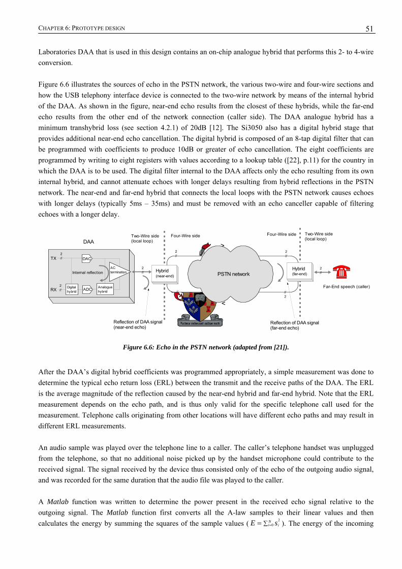
CHAPTER 6: PROTOTYPE DESIGN
51
Laboratories DAA that is used in this design contains an on-chip analogue hybrid that performs this 2- to 4-wire conversion. Figure 6.6 illustrates the sources of echo in the PSTN network, the various two-wire and four-wire sections and how the USB telephony interface device is connected to the two-wire network by means of the internal hybrid of the DAA. As shown in the figure, near-end echo results from the closest of these hybrids, while the far-end echo results from the other end of the network connection (caller side). The DAA analogue hybrid has a minimum transhybrid loss (see section 4.2.1) of 20dB [12]. The Si3050 also has a digital hybrid stage that provides additional near-end echo cancellation. The digital hybrid is composed of an 8-tap digital filter that can be programmed with coefficients to produce 10dB or greater of echo cancellation. The eight coefficients are programmed by writing to eight registers with values according to a lookup table ([22], p.11) for the country in which the DAA is to be used. The digital filter internal to the DAA affects only the echo resulting from its own internal hybrid, and cannot attenuate echoes with longer delays resulting from hybrid reflections in the PSTN network. The near-end and far-end hybrid that connects the local loops with the PSTN network causes echoes with longer delays (typically 5ms – 35ms) and must be removed with an echo canceller capable of filtering echoes with a longer delay.
Figure 6.6: Echo in the PSTN network (adapted from [21]).
After the DAA’s digital hybrid coefficients was programmed appropriately, a simple measurement was done to determine the typical echo return loss (ERL) between the transmit and the receive paths of the DAA. The ERL is the average magnitude of the reflection caused by the near-end hybrid and far-end hybrid. Note that the ERL measurement depends on the echo path, and is thus only valid for the specific telephone call used for the measurement. Telephone calls originating from other locations will have different echo paths and may result in different ERL measurements. An audio sample was played over the telephone line to a caller. The caller’s telephone handset was unplugged from the telephone, so that no additional noise picked up by the handset microphone could contribute to the received signal. The signal received by the device thus consisted only of the echo of the outgoing audio signal, and was recorded for the same duration that the audio file was played to the caller. A Matlab function was written to determine the power present in the received echo signal relative to the outgoing signal. The Matlab function first converts all the A-law samples to their linear values and then calculates the energy by summing the squares of the sample values ( 2
0Ni iE s=∑= ). The energy of the incoming
RX
TX
Hybrid(near-end)
Hybrid(far-end)
Two-Wire side(local loop)
Four-Wire side Four-Wire side Two-Wire side(local loop)
Far-End speech (caller)
Reflection of DAA signal(far-end echo)
Reflection of DAA signal(near-end echo)
Internal reflection
>
<
Analoguehybrid
Digitalhybrid
ACtermination
DAC
ADC
2//
2//
2//
//2
2//
PSTN network
2//
//2
2//
DAA

CHAPTER 6: PROTOTYPE DESIGN
52
and outgoing signals is then used to calculate the power of the incoming signal relative to the outgoing signal by using the following equation:
The incoming echo was recorded and measured to be -22.2dB relative to the outgoing signal. The ERL due to the echo path is thus 22.2dB. The ERL is not large enough to suppress the echo (the echo could clearly be heard), and further echo cancellation is required to make speech recognition and barge-in detection possible. According to studies, the echo signal is negligible when the ERL is approximately 55dB or more [25]. An additional echo canceller would typically provide 30dB to 40dB of echo return loss enhancement (ERLE). ERLE is a figure of merit for the amount of echo attenuation that an echo canceller can achieve.
6.3.2 Additional near-end and far-end echo cancellation The ITU-T defined several standards for echo cancellation. The most relevant of these are G.164, G.165, and G.168, which provides the basic guidelines for echo canceller functionality and performance. It is expected of echo cancellers to be compliant to these standards. Figure 6.7 (adapted from [24]) describes the signal flow in an echo canceller.
Echo canceller hybrid
+
y(i)A
B
C
caller speech
r(i)^-
+
u(i)=x(i) + r(i)- r(i)
e(i)x(i) + r(i)
DIncoming signal(caller signal + echo)
Outgoing signal
echo estimate
Compensated signal
x(i)
Figure 6.7: Echo canceller configuration (adapted from [24]).
First, the expected echo signal )(ˆ ir is estimated by comparing the outgoing signal )(iy with the incoming signal )()( irix + . The incoming signal consists of the caller’s speech )(ix and the echo )(ir of the outgoing signal. This is done by storing and comparing the outgoing and incoming signal for a period of time known as the “tail length”. The tail length should at least be the same as the total roundtrip echo delay. By comparing the incoming signal with the reference signal (outgoing signal), the echo path is measured and the result is used to adjust a transversal filter (tapped-delay line) that estimates and replicates the echo. The presumed echo signal is then subtracted from the incoming signal to remove the echo of the outgoing signal. The most echo cancellers use a long FIR (finite impulse response) transversal filter, and ideally the tap weights of the filter would be adjusted to match the impulse response of the echo path. Figure 6.8 (adapted from [24]) shows how echo estimation is accomplished using a transversal filter. A convergence algorithm is used to continuously adapt the filter coefficients (a0 to an-1) to minimise the cancellation error )(ie when no caller speech )(ix is present. The number of taps required in the transversal
)log(20out
in
EEPower =
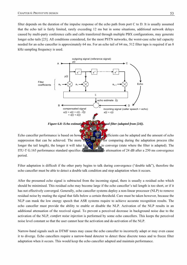
CHAPTER 6: PROTOTYPE DESIGN
53
filter depends on the duration of the impulse response of the echo path from port C to D. It is usually assumed that the echo tail is fairly limited, rarely exceeding 12 ms but in some situations, additional network delays caused by multi-party conference calls and calls transferred through multiple PBX configurations, may generate longer echo tails [23]. All conditions considered, for the most PSTN networks, the worst-case echo tail capacity needed for an echo canceller is approximately 64 ms. For an echo tail of 64 ms, 512 filter taps is required if an 8 kHz sampling frequency is used.
z-1 z-1 z-1
a0 a1 an-1
Σ
Echo
C
D
A
B
outgoing signal (reference signal)
y(i)
r(i)^-
+
x(i) + r(i)u(i) = x(i) + r(i) - r(i)^= x(i) + e(i)
y(i)
echo estimate
incoming signal (caller speech + echo)compensated signal
Filtercoefficients
Figure 6.8: Echo estimation using a transversal filter (adapted from [24]).
Echo canceller performance is based on how fast the filter’s coefficients can be adapted and the amount of echo suppression that can be achieved. The more samples used for comparing during the adaptation process (the longer the tail length), the longer it will take for the filter to converge (state where the filter is adapted). The ITU-T G.165 performance standard specifies a minimum echo attenuation of 24 dB after a 250 ms convergence period. Filter adaptation is difficult if the other party begins to talk during convergence (“double talk”), therefore the echo canceller must be able to detect a double talk condition and stop adaptation when it occurs. After the presumed echo signal is subtracted from the incoming signal, there is usually a residual echo which should be minimised. This residual echo may become large if the echo canceller’s tail length is too short, or if it has not effectively converged. Generally, echo canceller systems deploy a non-linear processor (NLP) to remove residual noise by muting the signal that falls below a certain threshold. Care must be taken however, because the NLP can mask the low energy speech that ASR systems require to achieve accurate recognition results. The echo canceller must provide the ability to enable or disable the NLP. Activation of the NLP results in an additional attenuation of the received signal. To prevent a perceived decrease in background noise due to the activation of the NLP, comfort noise injection is performed by some echo cancellers. This keeps the perceived noise level constant so that the user cannot hear the activation and de-activation of the NLP. Narrow-band signals such as DTMF tones may cause the echo canceller to incorrectly adapt or may even cause it to diverge. Echo cancellers require a narrow-band detector to detect these discrete tones and to freeze filter adaptation when it occurs. This would keep the echo canceller adapted and maintain performance.

CHAPTER 6: PROTOTYPE DESIGN
54
Echo cancellation can be software-based or hardware-based. In this project, it would be preferred if echo cancellation could be done in the hardware device itself, as it is the only location where the incoming and outgoing signals are synchronised and available in real-time. Software-based echo cancellers are designed to run on DSP processors because of their high computational demand and a general-purpose CPU (like our 8051 microcontroller) would not be suitable for this purpose. A DSP processor would increase the cost and complexity of our design. Hardware-based echo cancellers include FPGA-based echo cancellers and application specific integrated circuit (ASIC) echo cancellers. ASICs are usually cheaper and provide better performance than a DSP or a FPGA solution, as the circuit has been specifically designed to perform echo cancellation. Infineon, OKI semiconductor and Zarlink semiconductor are manufacturers of ASIC echo cancellers. A 2-channel echo canceller is required for the two telephony channels in the prototype design. OKI has a 2-channel echo canceller available (MSM7617), but the device has no microcontroller interface available, whilst Zarlink’s MT9123 2-channel echo canceller can be used in a “controller” or “controllerless” mode. Controller mode allows microcontroller access to features and allows customising the behaviour of the device. The following section describes the features of the Zarlink MT9123 echo canceller, and how the first prototype was adapted to integrate the echo canceller into the design.
6.3.3 Zarlink MT9123 2-channel echo canceller This device conforms to all the requirements of an echo canceller, as described in the previous section. To summarise, each echo canceller of the Zarlink MT9123 contains the following elements [25]:
• Adaptive filter for estimating and cancelling the echo. • Double-talk detector with programmable threshold for disabling the filter adaptation during periods of
double-talk. • Non-linear processor (NLP) with comfort noise injection for suppression of residual echo. The NLP can
be disabled. • Narrow-band detector for disabling the filter adaptation and preventing divergence caused by narrow-
band signals. • Offset null filters for removing the DC component in the PCM signals. • Optional 12dB attenuator for signal attenuation. Disabled by default. • Serial peripheral interface (SPI), compatible with Motorola, National and Intel microcontrollers. • PCM encoder and decoder compatible with μ-law/ A-law coding.
The echo canceller provides 64 ms of echo cancellation for two channels, or the two echo cancellers may be configured to provide 128ms of echo cancellation for a single channel. Figure 6.9 (from [25], p. 1) illustrates the elements of the Zarlink echo canceller. The echo canceller has four functional states: Mute, Bypass, Disable Adaptation and Enable Adaptation. The Mute state forces the echo canceller to transmit “quiet code” for the PCM output data and halts the filter adaptation process. The value of the quiet code depends on the companding method used. The Bypass state directly transfers the PCM signal from Rin to Rout and from Sin to Sout (refer to Figure 6.9). If the Disable Adaptation state is selected, the filter coefficients are frozen at the current values, but the echo canceller continues to cancel echo. Enable Adaptation is the normal operating state, where the adaptive filter coefficients are continually updated to model the echo return path. The two echo cancellers operate independently of each

CHAPTER 6: PROTOTYPE DESIGN
55
other. In controller mode, the functional states of the echo cancellers can be selected by adjusting the control registers. The register summary ([25], p.17) contains the details of these registers.
Figure 6.9: Zarlink MT9123 echo canceller (from [25], p.1).
Adaptive filters in general do not operate correctly if a DC offset is present in the reference (Rin) or incoming signal (Sin). The Zarlink echo canceller incorporates offset null filters in both inputs to remove the DC component from the PCM signal.
6.3.4 Hardware design Figure 6.10 shows a conceptual diagram of the second prototype, which illustrates how the echo canceller was integrated into the design.
Figure 6.10: Conceptual diagram of the second prototype.
Cypress EZ-USBFX microcontroller
CypressCPLD 128kb RAM
Address16-bit
Data8-bit
USB
Development board
Slave FIFO buffersAltera CPLD
SiliconLabs DAA
Si3050
SiliconLabs DAA
Si3050
SiliconLabs DAA
Si3019
SiliconLabs DAA
Si3019
Telephone line
Telephone line
PCM bus
8.192 MHzoscillator
SPI bus
Mating board
Isolation Barrier
//8
Zarlink MT9123Echo Canceller
20 MHzoscillator
PCM
enable strobesignals
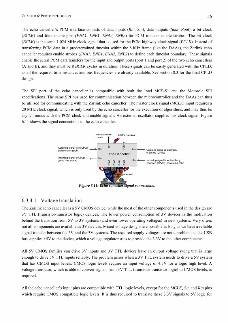
CHAPTER 6: PROTOTYPE DESIGN
56
Rin
Sin
Rout
Sout
ENA1
ENA2
ENB1
ENB2
Echo CancellerOutgoing signal to telephonychannels (DAAs)
Incoming signal from telephonychannels (DAAs), containing echo
enable strobes generatedby the CPLD
Outgoing signal from CPLD(reference signal)
Incoming signal to CPLD(echo free signal)
SPI
microcontrollercontrol
MC
LK
20Mhz oscillator
The echo canceller’s PCM interface consists of data inputs (Rin, Sin), data outputs (Sout, Rout), a bit clock (BCLK) and four enable pins (ENA1, ENB1, ENA2, ENB2) for PCM transfer enable strobes. The bit clock (BCLK) is the same 1.024 MHz clock signal that is used for the PCM highway clock signal (PCLK). Instead of transferring PCM data in a predetermined timeslot within the 8 kHz frame (like the DAAs), the Zarlink echo canceller requires enable strobes (ENA1, ENB1, ENA2, ENB2) to define each timeslot boundary. These signals enable the serial PCM data transfers for the input and output ports (port 1 and port 2) of the two echo cancellers (A and B), and they must be 8 BCLK cycles in duration. These signals can be easily generated with the CPLD, as all the required time instances and bus frequencies are already available. See section 8.3 for the final CPLD design. The SPI port of the echo canceller is compatible with both the Intel MCS-51 and the Motorola SPI specifications. The same SPI bus used for communication between the microcontroller and the DAAs can thus be utilised for communicating with the Zarlink echo canceller. The master clock signal (MCLK) input requires a 20 MHz clock signal, which is only used by the echo canceller for the execution of algorithms, and may thus be asynchronous with the PCM clock and enable signals. An external oscillator supplies this clock signal. Figure 6.11 shows the signal connections to the echo canceller.
Figure 6.11: Echo canceller signal connections.
6.3.4.1 Voltage translation The Zarlink echo canceller is a 5V CMOS device, while the most of the other components used in the design are 3V TTL (transistor-transistor logic) devices. The lower power consumption of 3V devices is the motivation behind the transition from 5V to 3V systems (and even lower operating voltages) in new systems. Very often, not all components are available as 3V devices. Mixed voltage designs are possible as long as we have a reliable signal transfer between the 5V and the 3V systems. The required supply voltages are not a problem, as the USB bus supplies +5V to the device, which a voltage regulator uses to provide the 3.3V to the other components. All 5V CMOS families can drive 3V inputs and 3V TTL devices have an output voltage swing that is large enough to drive 5V TTL inputs reliably. The problem arises when a 3V TTL system needs to drive a 5V system that has CMOS input levels. CMOS logic levels require an input voltage of 4.5V for a logic high level. A voltage translator, which is able to convert signals from 3V TTL (transistor-transistor logic) to CMOS levels, is required. All the echo canceller’s input pins are compatible with TTL logic levels, except for the MCLK, Sin and Rin pins which require CMOS compatible logic levels. It is thus required to translate these 3.3V signals to 5V logic for
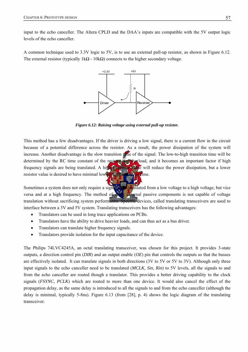
CHAPTER 6: PROTOTYPE DESIGN
57
+3.3V +5V
R
Driver Receiver
input to the echo canceller. The Altera CPLD and the DAA’s inputs are compatible with the 5V output logic levels of the echo canceller. A common technique used to 3.3V logic to 5V, is to use an external pull-up resistor, as shown in Figure 6.12. The external resistor (typically 1kΩ - 10kΩ) connects to the higher secondary voltage.
Figure 6.12: Raising voltage using external pull-up resistor.
This method has a few disadvantages. If the driver is driving a low signal, there is a current flow in the circuit because of a potential difference across the resistor. As a result, the power dissipation of the system will increase. Another disadvantage is the slow transition time of the signal. The low-to-high transition time will be determined by the RC time constant of the resistor and the load, and it becomes an important factor if high frequency signals are being translated. A higher resistor value will reduce the power dissipation, but a lower resistor value is desired to have minimal low-to-high transition time. Sometimes a system does not only require a signal to be translated from a low voltage to a high voltage, but vice versa and at a high frequency. The method of using external passive components is not capable of voltage translation without sacrificing system performance. Specific devices, called translating transceivers are used to interface between a 3V and 5V system. Translating transceivers has the following advantages:
• Translators can be used in long trace applications on PCBs. • Translators have the ability to drive heavier loads, and can thus act as a bus driver. • Translators can translate higher frequency signals. • Translators provide isolation for the input capacitance of the device.
The Philips 74LVC4245A, an octal translating transceiver, was chosen for this project. It provides 3-state outputs, a direction control pin (DIR) and an output enable (OE) pin that controls the outputs so that the busses are effectively isolated. It can translate signals in both directions (3V to 5V or 5V to 3V). Although only three input signals to the echo canceller need to be translated (MCLK, Sin, Rin) to 5V levels, all the signals to and from the echo canceller are routed though a translator. This provides a better driving capability to the clock signals (FSYNC, PCLK) which are routed to more than one device. It would also cancel the effect of the propagation delay, as the same delay is introduced to all the signals to and from the echo canceller (although the delay is minimal, typically 5-8ns). Figure 6.13 (from [28], p. 4) shows the logic diagram of the translating transceiver.
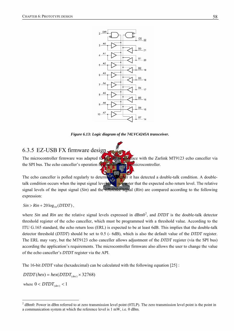
CHAPTER 6: PROTOTYPE DESIGN
58
Figure 6.13: Logic diagram of the 74LVC4245A transceiver.
6.3.5 EZ-USB FX firmware design The microcontroller firmware was adapted to be able to interface with the Zarlink MT9123 echo canceller via the SPI bus. The echo canceller’s operation is controlled by the microcontroller. The echo canceller is polled regularly to determine whether it has detected a double-talk condition. A double-talk condition occurs when the input signal level (Sin) is greater that the expected echo return level. The relative signal levels of the input signal (Sin) and the reference signal (Rin) are compared according to the following expression:
)(log20 10 DTDTRinSin +> ,
where Sin and Rin are the relative signal levels expressed in dBm02, and DTDT is the double-talk detector threshold register of the echo canceller, which must be programmed with a threshold value. According to the ITU G.165 standard, the echo return loss (ERL) is expected to be at least 6dB. This implies that the double-talk detector threshold (DTDT) should be set to 0.5 (- 6dB), which is also the default value of the DTDT register. The ERL may vary, but the MT9123 echo canceller allows adjustment of the DTDT register (via the SPI bus) according the application’s requirements. The microcontroller firmware also allows the user to change the value of the echo canceller’s DTDT register via the API. The 16-bit DTDT value (hexadecimal) can be calculated with the following equation [25] :
)32768()( )( ×= decDTDThexhexDTDT
where 10 )( << decDTDT
2 dBm0: Power in dBm referred to at zero transmission level point (0TLP). The zero transmission level point is the point in a communication system at which the reference level is 1 mW, i.e. 0 dBm.
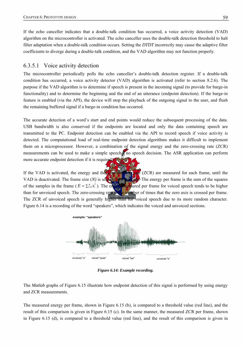
CHAPTER 6: PROTOTYPE DESIGN
59
If the echo canceller indicates that a double-talk condition has occurred, a voice activity detection (VAD) algorithm on the microcontroller is activated. The echo canceller uses the double-talk detection threshold to halt filter adaptation when a double-talk condition occurs. Setting the DTDT incorrectly may cause the adaptive filter coefficients to diverge during a double-talk condition, and the VAD algorithm may not function properly.
6.3.5.1 Voice activity detection The microcontroller periodically polls the echo canceller’s double-talk detection register. If a double-talk condition has occurred, a voice activity detector (VAD) algorithm is activated (refer to section 8.2.6). The purpose if the VAD algorithm is to determine if speech is present in the incoming signal (to provide for barge-in functionality) and to determine the beginning and the end of an utterance (endpoint detection). If the barge-in feature is enabled (via the API), the device will stop the playback of the outgoing signal to the user, and flush the remaining buffered signal if a barge-in condition has occurred. The accurate detection of a word’s start and end points would reduce the subsequent processing of the data. USB bandwidth is also conserved if the endpoints are located and only the data containing speech are transmitted to the PC. Endpoint detection can be enabled via the API to record speech if voice activity is detected. The computational load of real-time endpoint detection algorithms makes it difficult to implement them on a microprocessor. However, a combination of the signal energy and the zero-crossing rate (ZCR) measurements can be used to make a simple speech / no speech decision. The ASR application can perform more accurate endpoint detection if it is required. If the VAD is activated, the energy and the zero-crossing rate (ZCR) are measured for each frame, until the VAD is deactivated. The frame size (N) is usually 128 samples. The energy per frame is the sum of the squares of the samples in the frame ( 2
0Ni iE s=∑= ). The energy measured per frame for voiced speech tends to be higher
than for unvoiced speech. The zero-crossing rate is the number of times that the zero axis is crossed per frame. The ZCR of unvoiced speech is generally higher than for voiced speech due to its more random character. Figure 6.14 is a recording of the word “speakers”, which indicates the voiced and unvoiced sections.
unvoiced "s" voiced "spea" voiced "ker" unvoiced "s"
example: "speakers"
Figure 6.14: Example recording.
The Matlab graphs of Figure 6.15 illustrate how endpoint detection of this signal is performed by using energy and ZCR measurements. The measured energy per frame, shown in Figure 6.15 (b), is compared to a threshold value (red line), and the result of this comparison is given in Figure 6.15 (c). In the same manner, the measured ZCR per frame, shown in Figure 6.15 (d), is compared to a threshold value (red line), and the result of this comparison is given in
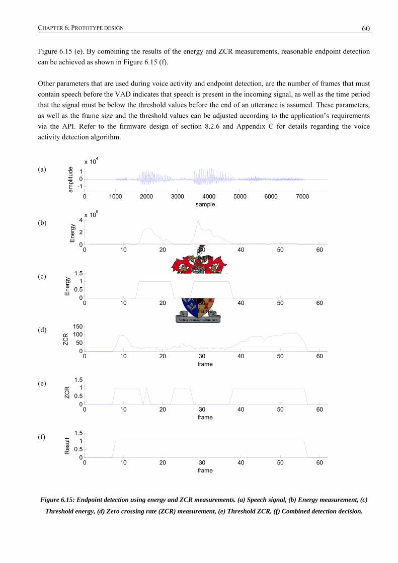
CHAPTER 6: PROTOTYPE DESIGN
60
Figure 6.15 (e). By combining the results of the energy and ZCR measurements, reasonable endpoint detection can be achieved as shown in Figure 6.15 (f). Other parameters that are used during voice activity and endpoint detection, are the number of frames that must contain speech before the VAD indicates that speech is present in the incoming signal, as well as the time period that the signal must be below the threshold values before the end of an utterance is assumed. These parameters, as well as the frame size and the threshold values can be adjusted according to the application’s requirements via the API. Refer to the firmware design of section 8.2.6 and Appendix C for details regarding the voice activity detection algorithm. (a) (b) (c) (d) (e) (f)
Figure 6.15: Endpoint detection using energy and ZCR measurements. (a) Speech signal, (b) Energy measurement, (c)
Threshold energy, (d) Zero crossing rate (ZCR) measurement, (e) Threshold ZCR, (f) Combined detection decision.
0 1000 2000 3000 4000 5000 6000 7000
-101
x 104
sample
ampl
itude
0 10 20 30 40 50 600
2
4x 10⁹
Ene
rgy
frame
0 10 20 30 40 50 600
0.51
1.5
Ene
rgy
frame
0 10 20 30 40 50 600
50100150
ZCR
frame
0 10 20 30 40 50 600
0.51
1.5
ZCR
frame
0 10 20 30 40 50 600
0.51
1.5
Res
ult
frame
CHAPTER 6: PROTOTYPE DESIGN
61
6.3.6 CPLD firmware design The CPLD firmware is adapted to provide the additional data transfer enable strobes (ENA1, ENB1, ENA2, ENB2) required by the echo canceller, as shown in Figure 6.12. These strobes are synchronised with the FSYNC and PCLK PCM highway timing signals routed to the DAAs, and they must coincide with the DAA’s pre-programmed timeslot allocations for PCM data transfers. The strobes are each 8 PCLK (BCLK) clock cycles in length. Refer to the CPLD design in section 8.3 for more details.
6.3.7 Prototype results The measurement that was performed in section 6.3.1 (before the echo canceller was added) was repeated to determine the amount of echo suppression that the Zarlink echo canceller provided. Initially, the echo canceller did not perform as expected. It was slow to converge, and echo suppression was poor. This problem was due to a gain that was applied in the DAA to the transmitted signal, which caused the signal to be slightly clipped when it reached the maximum output swing capabilities of the DAA circuit. The signal transmitted on the telephone line therefore differed from the reference signal supplied to the echo canceller, which also meant that the received echo signal did not match the estimated echo signal. The problem was corrected by disabling the transmit path gain of the DAA. The incoming signal level (after the echo canceller) relative to the outgoing signal level was measured to be -60.1dB. The ERLE for the echo canceller is thus 37.9dB. This is satisfactory performance for an echo canceller, and no remaining echo could be heard in the incoming signal. The voice activity detection (endpoint detection and barge-in detection) was tested by developing a simple dialogue test application. A problem was found with the ZCR measurement. The echo canceller only attenuated the echo in the signal, but the zero-crossing rate information of the outgoing signal was still present in the incoming signal. To prevent the voice activity detector from detecting the echoed ZCR information, the signal energy was also considered when performing the ZCR measurements. This ensures that the ZCR measurement was only applicable to the user speech. The ZCR measurement could however be compromised during a barge-in condition, when both system and user speech ZCR information is present in the incoming signal. In such a case, the ZCR measurement could be higher than expected, making endpoint detection more sensitive to the ZCR measurement. The ZCR measurement could be adapted during double-talk conditions, but testing of the device during barge-in conditions concluded that this effect was negligible, as no loss in endpoint and voice activity detection performance could be observed. The 128K of RAM on the development board is not large enough to store the firmware code and to buffer enough incoming and outgoing telephony data. A 512K RAM chip must be used in the final prototype design. This would allow buffering of at least 6 to 8 seconds of data for both incoming and outgoing data (for both telephony channels). The CPLD and microcontroller firmware would need to be adapted so that memory bank switching can be performed. Finally, the firmware for the final prototype device must be adapted so that it would be able to transfer an incoming call to another telephone number. It must be possible to transfer a call using an external PBX or by relaying the call through the second telephone channel of the device (refer to section 8.2.4).
Chapter 7
7. Final prototype: hardware design
Final prototype: hardware design
The final prototype includes all the components, design aspects and solutions of the previous prototypes, but is designed as a stand-alone device so that the development board is no longer required. The result of this chapter is a schematic design (Appendix A), and it is used to design the Printed Circuit Board (PCB). Refer to Appendix B for the PCB design considerations and layout. The schematic design is a logical representation of the hardware device that includes all components and electrical connections. The Protel 99 SE software suite was used to create the schematic design entries. The following steps are performed in order to create the schematic design:
1. Logic symbols are created for each of the components used. 2. Annotation of components (assigning designators and footprints to the parts). 3. Creation of all electrical connections between components. 4. Verification of the schematic design. Verification is done by using Protel’s Electrical Rule Checker
(ERC). The ERC examines the schematic design for electrical inconsistencies (short circuits, floating pins etc.) and drafting inconsistencies (duplicate designators, unconnected net labels etc.).
The following sections describe the design of the final prototype device. Although the schematic entries are discussed individually, signal interconnections exist between the schematic entries using net labels (red text in the schematic entries). Net labels connect a wire or pin to another wire or pin elsewhere in the design with the same net label. The complete circuit schematic can be found in Appendix A.
7.1 User I/O interface The only user I/O provided are LEDs and a button to reset the USB device.
7.1.1 LEDs Light-emitting diodes (LEDs) are required to display the device’s current status, and to signal error conditions. A bank of 6 HSMH C650 surface mount LEDs (red and green) is connected to I/O pins of the EZ-USB FX. The maximum output current of an EZ-USB FX pin is 10 mA [4]. To keep power dissipation to a minimum, we limit the current though a LED at 4 mA. According to the LED datasheet, the forward voltage ( fV ) is approximately 1.7 V at a forward current ( fI ) of 4 mA [32]. This implies a voltage drop of 1.6 V across the series current limiting resistor (see schematic entry of Figure 7.1). The value of this resistor should be:
Ω=×
== − 4001046.1
3IVR
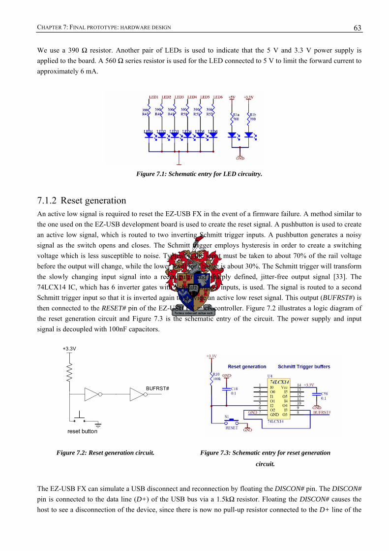
CHAPTER 7: FINAL PROTOTYPE: HARDWARE DESIGN
63
We use a 390 Ω resistor. Another pair of LEDs is used to indicate that the 5 V and 3.3 V power supply is applied to the board. A 560 Ω series resistor is used for the LED connected to 5 V to limit the forward current to approximately 6 mA.
Figure 7.1: Schematic entry for LED circuitry.
7.1.2 Reset generation An active low signal is required to reset the EZ-USB FX in the event of a firmware failure. A method similar to the one used on the EZ-USB development board is used to create the reset signal. A pushbutton is used to create an active low signal, which is routed to two inverting Schmitt trigger inputs. A pushbutton generates a noisy signal as the switch opens and closes. The Schmitt trigger employs hysteresis in order to create a switching voltage which is less susceptible to noise. Typically, the input must be taken to about 70% of the rail voltage before the output will change, while the lower level for change is about 30%. The Schmitt trigger will transform the slowly changing input signal into a rectangular and sharply defined, jitter-free output signal [33]. The 74LCX14 IC, which has 6 inverter gates with Schmitt trigger inputs, is used. The signal is routed to a second Schmitt trigger input so that it is inverted again to provide an active low reset signal. This output (BUFRST#) is then connected to the RESET# pin of the EZ-USB FX microcontroller. Figure 7.2 illustrates a logic diagram of the reset generation circuit and Figure 7.3 is the schematic entry of the circuit. The power supply and input signal is decoupled with 100nF capacitors.
Figure 7.2: Reset generation circuit.
Figure 7.3: Schematic entry for reset generation
circuit.
The EZ-USB FX can simulate a USB disconnect and reconnection by floating the DISCON# pin. The DISCON# pin is connected to the data line (D+) of the USB bus via a 1.5kΩ resistor. Floating the DISCON# causes the host to see a disconnection of the device, since there is now no pull-up resistor connected to the D+ line of the
+3.3V
BUFRST#
reset button
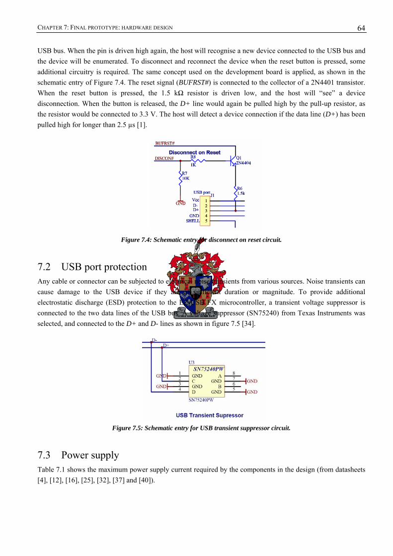
CHAPTER 7: FINAL PROTOTYPE: HARDWARE DESIGN
64
USB bus. When the pin is driven high again, the host will recognise a new device connected to the USB bus and the device will be enumerated. To disconnect and reconnect the device when the reset button is pressed, some additional circuitry is required. The same concept used on the development board is applied, as shown in the schematic entry of Figure 7.4. The reset signal (BUFRST#) is connected to the collector of a 2N4401 transistor. When the reset button is pressed, the 1.5 kΩ resistor is driven low, and the host will “see” a device disconnection. When the button is released, the D+ line would again be pulled high by the pull-up resistor, as the resistor would be connected to 3.3 V. The host will detect a device connection if the data line (D+) has been pulled high for longer than 2.5 µs [1].
Figure 7.4: Schematic entry for disconnect on reset circuit.
7.2 USB port protection Any cable or connector can be subjected to electrical noise transients from various sources. Noise transients can cause damage to the USB device if they are of sufficient duration or magnitude. To provide additional electrostatic discharge (ESD) protection to the EZ-USB FX microcontroller, a transient voltage suppressor is connected to the two data lines of the USB bus. A voltage suppressor (SN75240) from Texas Instruments was selected, and connected to the D+ and D- lines as shown in figure 7.5 [34].
Figure 7.5: Schematic entry for USB transient suppressor circuit.
7.3 Power supply Table 7.1 shows the maximum power supply current required by the components in the design (from datasheets [4], [12], [16], [25], [32], [37] and [40]).
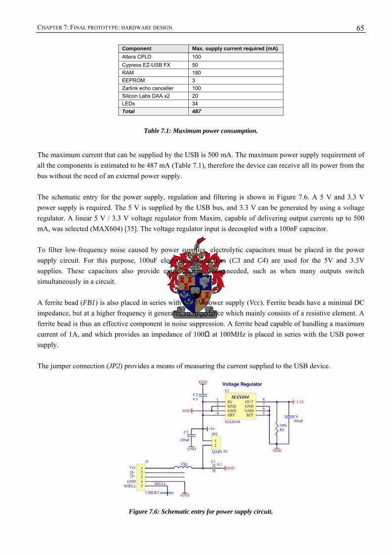
CHAPTER 7: FINAL PROTOTYPE: HARDWARE DESIGN
65
Component Max. supply current required (mA) Altera CPLD 100 Cypress EZ-USB FX 50 RAM 180 EEPROM 3 Zarlink echo canceller 100 Silicon Labs DAA x2 20 LEDs 34 Total 487
Table 7.1: Maximum power consumption.
The maximum current that can be supplied by the USB is 500 mA. The maximum power supply requirement of all the components is estimated to be 487 mA (Table 7.1), therefore the device can receive all its power from the bus without the need of an external power supply. The schematic entry for the power supply, regulation and filtering is shown in Figure 7.6. A 5 V and 3.3 V power supply is required. The 5 V is supplied by the USB bus, and 3.3 V can be generated by using a voltage regulator. A linear 5 V / 3.3 V voltage regulator from Maxim, capable of delivering output currents up to 500 mA, was selected (MAX604) [35]. The voltage regulator input is decoupled with a 100nF capacitor. To filter low-frequency noise caused by power supplies, electrolytic capacitors must be placed in the power supply circuit. For this purpose, 100uF electrolytic capacitors (C3 and C4) are used for the 5V and 3.3V supplies. These capacitors also provide extra current when needed, such as when many outputs switch simultaneously in a circuit. A ferrite bead (FB1) is also placed in series with the 5V power supply (Vcc). Ferrite beads have a minimal DC impedance, but at a higher frequency it generates an impedance which mainly consists of a resistive element. A ferrite bead is thus an effective component in noise suppression. A ferrite bead capable of handling a maximum current of 1A, and which provides an impedance of 100Ω at 100MHz is placed in series with the USB power supply. The jumper connection (JP2) provides a means of measuring the current supplied to the USB device.
Figure 7.6: Schematic entry for power supply circuit.
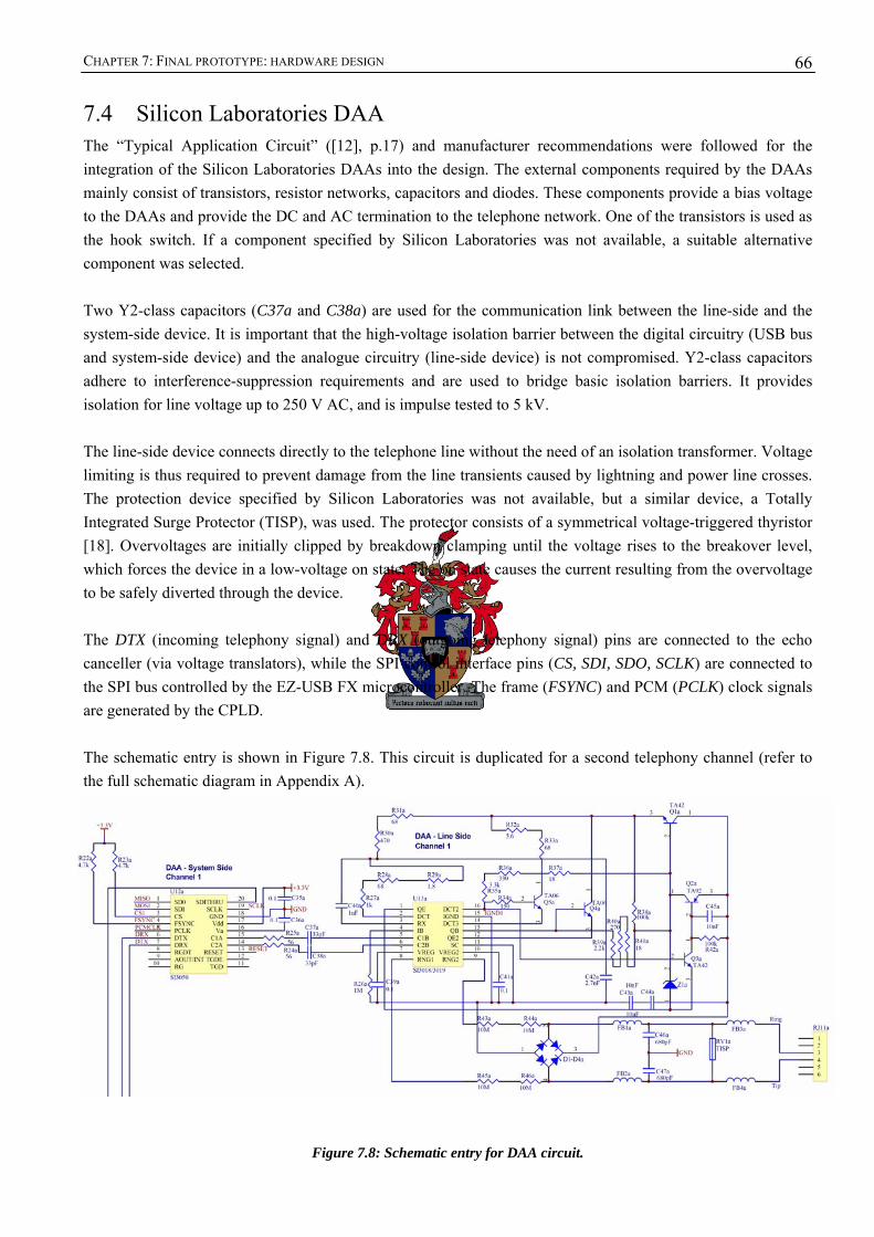
CHAPTER 7: FINAL PROTOTYPE: HARDWARE DESIGN
66
7.4 Silicon Laboratories DAA The “Typical Application Circuit” ([12], p.17) and manufacturer recommendations were followed for the integration of the Silicon Laboratories DAAs into the design. The external components required by the DAAs mainly consist of transistors, resistor networks, capacitors and diodes. These components provide a bias voltage to the DAAs and provide the DC and AC termination to the telephone network. One of the transistors is used as the hook switch. If a component specified by Silicon Laboratories was not available, a suitable alternative component was selected. Two Y2-class capacitors (C37a and C38a) are used for the communication link between the line-side and the system-side device. It is important that the high-voltage isolation barrier between the digital circuitry (USB bus and system-side device) and the analogue circuitry (line-side device) is not compromised. Y2-class capacitors adhere to interference-suppression requirements and are used to bridge basic isolation barriers. It provides isolation for line voltage up to 250 V AC, and is impulse tested to 5 kV. The line-side device connects directly to the telephone line without the need of an isolation transformer. Voltage limiting is thus required to prevent damage from the line transients caused by lightning and power line crosses. The protection device specified by Silicon Laboratories was not available, but a similar device, a Totally Integrated Surge Protector (TISP), was used. The protector consists of a symmetrical voltage-triggered thyristor [18]. Overvoltages are initially clipped by breakdown clamping until the voltage rises to the breakover level, which forces the device in a low-voltage on state. The on state causes the current resulting from the overvoltage to be safely diverted through the device. The DTX (incoming telephony signal) and DRX (outgoing telephony signal) pins are connected to the echo canceller (via voltage translators), while the SPI control interface pins (CS, SDI, SDO, SCLK) are connected to the SPI bus controlled by the EZ-USB FX microcontroller. The frame (FSYNC) and PCM (PCLK) clock signals are generated by the CPLD. The schematic entry is shown in Figure 7.8. This circuit is duplicated for a second telephony channel (refer to the full schematic diagram in Appendix A).
Figure 7.8: Schematic entry for DAA circuit.

CHAPTER 7: FINAL PROTOTYPE: HARDWARE DESIGN
67
7.5 Altera CPLD To comply with the operating requirements for Altera devices, a general-purpose 100uF electrolytic capacitor is used to stabilise the power supply and 100nF ceramic capacitors are used between Vcc (positive power supply) and the ground plane at each Vcc pin [17]. The MaxPlus compiler generates a device utilisation report file, which provides information regarding the pin-outs and connectivity of the device used in the project, including the dedicated and unused pins. An 8.192 MHz clock oscillator ([36]) is connected to device’s global clock 1 pin (GCLK1), and the 48 MHz clock output signal from the EZ-USB FX is connected to the global clock 2 pin (GCLK2). A small resistor (22 Ω) is placed in series with the switching outputs (FSYNC, PCLK) to reduce noise. A JTAG programming interface is required to program the CPLD. The four JTAG signals (TDI, TMS, TDO, TCK) is routed to an 8 x 2 header connection, where a compatible programmer can be connected to the board.
Figure 7.9: Schematic entry for Altera CPLD circuit.
7.6 EZ-USB FX microcontroller The EZ-USB FX requires very few external components. All power supply pins (Vcc) are decoupled with 100nF capacitors. The USB data lines (D+ and D-) and the clock output pin (CLKOUT) are connected via 22 Ω resistors to reduce noise on these high-frequency lines. A 12 MHz series-resonant, fundamental mode crystal is connected between the XIN and XOUT pins, as well as two 33 pF capacitors connected to ground. A 1 MΩ resistor must also be connected between these pins. The I/O pins of the microcontroller are used for the LEDs, FIFO buffer I/O, control pins connected to the CPLD and the SPI bus. The address (A0-A15) and data lines are connected to the static RAM. The RESET# pin of the microcontroller is connected to the reset generation circuit. Three additional I/O pins used for the higher
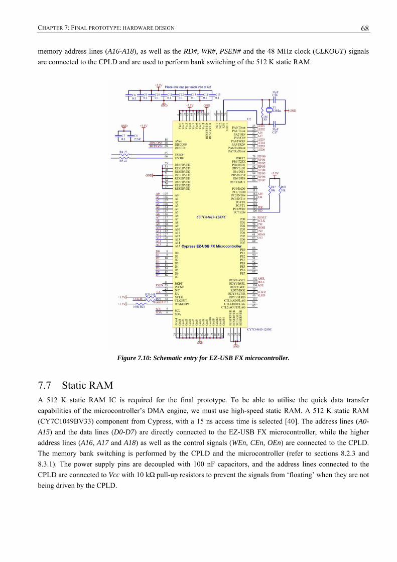
CHAPTER 7: FINAL PROTOTYPE: HARDWARE DESIGN
68
memory address lines (A16-A18), as well as the RD#, WR#, PSEN# and the 48 MHz clock (CLKOUT) signals are connected to the CPLD and are used to perform bank switching of the 512 K static RAM.
Figure 7.10: Schematic entry for EZ-USB FX microcontroller.
7.7 Static RAM A 512 K static RAM IC is required for the final prototype. To be able to utilise the quick data transfer capabilities of the microcontroller’s DMA engine, we must use high-speed static RAM. A 512 K static RAM (CY7C1049BV33) component from Cypress, with a 15 ns access time is selected [40]. The address lines (A0-A15) and the data lines (D0-D7) are directly connected to the EZ-USB FX microcontroller, while the higher address lines (A16, A17 and A18) as well as the control signals (WEn, CEn, OEn) are connected to the CPLD. The memory bank switching is performed by the CPLD and the microcontroller (refer to sections 8.2.3 and 8.3.1). The power supply pins are decoupled with 100 nF capacitors, and the address lines connected to the CPLD are connected to Vcc with 10 kΩ pull-up resistors to prevent the signals from ‘floating’ when they are not being driven by the CPLD.

CHAPTER 7: FINAL PROTOTYPE: HARDWARE DESIGN
69
Figure 7.11: Schematic entry for static RAM circuitry.
7.8 EEPROM The EZ-USB FX microcontroller requires an I2C serial EEPROM, connected to its I2C port, to store the device descriptors and the boot loader firmware. A 64K I2C serial EEPROM from Microchip is selected [37]. This is a double-address-byte (16-bit) EEPROM and the I2C controller of the EZ-USB FX needs to identify the EEPROM as such. A double-address-byte EEPROM’s address pins must be strapped to ‘001’ (A2, A1, A0) [38]. The I2C lines (SCL, SDA) require 1 kΩ pull-up resistors.
Figure 7.12: Schematic entry for EEPROM circuitry.
7.9 Zarlink MT9123 echo canceller The echo canceller requires a 20 MHz clock input which is provided by a clock oscillator. All signals to and from the echo canceller are translated by two voltage translators (see section 6.3.4.1). Although the translator’s direction of translation can be changed by toggling the DIR pin, we use two translators with fixed translation directions. One translator is used for the echo canceller’s input signals (3 V to 5 V) and the other translator is used for the echo canceller’s output signals (5 V to 3 V)
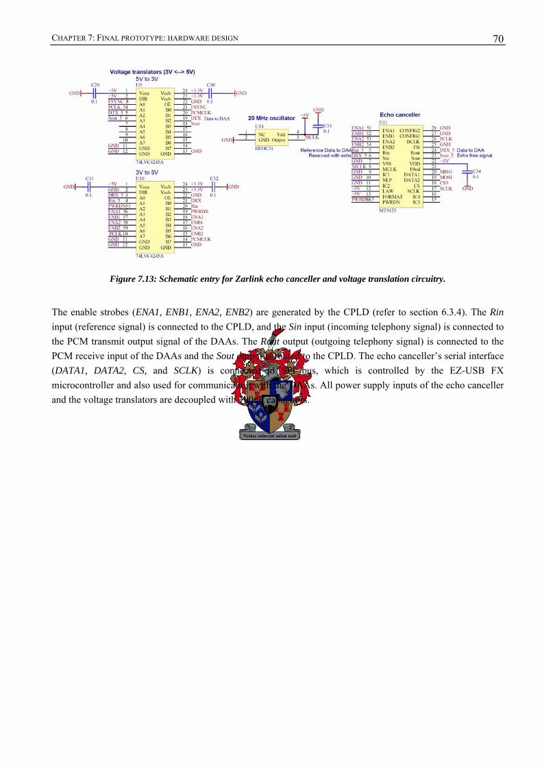
CHAPTER 7: FINAL PROTOTYPE: HARDWARE DESIGN
70
Figure 7.13: Schematic entry for Zarlink echo canceller and voltage translation circuitry.
The enable strobes (ENA1, ENB1, ENA2, ENB2) are generated by the CPLD (refer to section 6.3.4). The Rin input (reference signal) is connected to the CPLD, and the Sin input (incoming telephony signal) is connected to the PCM transmit output signal of the DAAs. The Rout output (outgoing telephony signal) is connected to the PCM receive input of the DAAs and the Sout output is routed to the CPLD. The echo canceller’s serial interface (DATA1, DATA2, CS, and SCLK) is connected to SPI bus, which is controlled by the EZ-USB FX microcontroller and also used for communication with the DAAs. All power supply inputs of the echo canceller and the voltage translators are decoupled with 100nF capacitors.
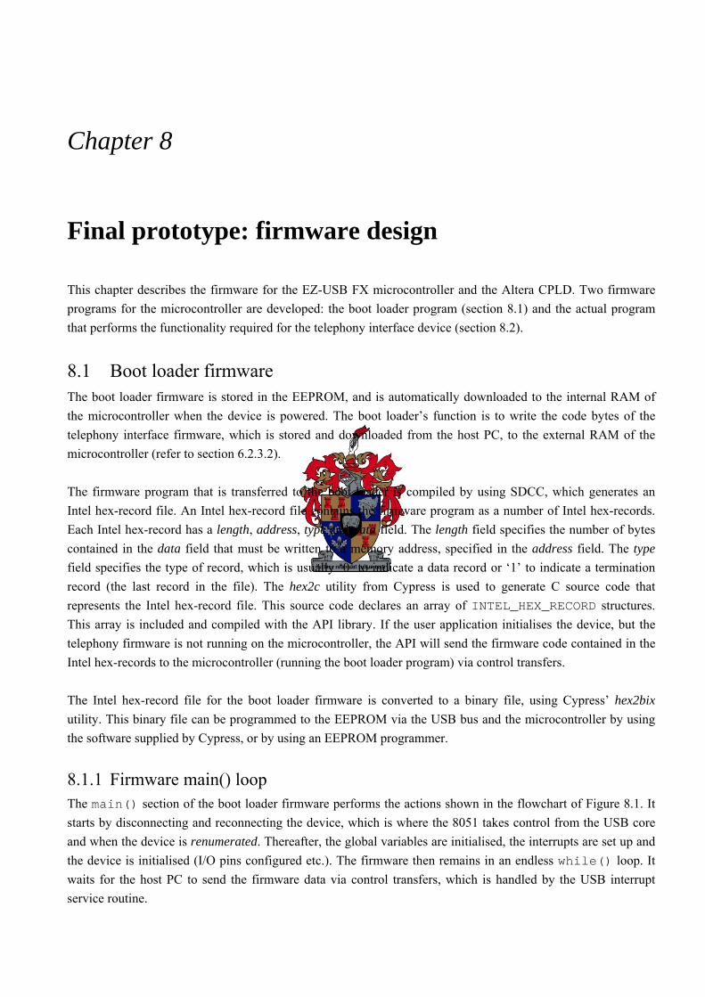
Chapter 8
8. Final prototype: firmware design
Final prototype: firmware design This chapter describes the firmware for the EZ-USB FX microcontroller and the Altera CPLD. Two firmware programs for the microcontroller are developed: the boot loader program (section 8.1) and the actual program that performs the functionality required for the telephony interface device (section 8.2).
8.1 Boot loader firmware The boot loader firmware is stored in the EEPROM, and is automatically downloaded to the internal RAM of the microcontroller when the device is powered. The boot loader’s function is to write the code bytes of the telephony interface firmware, which is stored and downloaded from the host PC, to the external RAM of the microcontroller (refer to section 6.2.3.2). The firmware program that is transferred to the boot loader is compiled by using SDCC, which generates an Intel hex-record file. An Intel hex-record file contains the firmware program as a number of Intel hex-records. Each Intel hex-record has a length, address, type and data field. The length field specifies the number of bytes contained in the data field that must be written to a memory address, specified in the address field. The type field specifies the type of record, which is usually ‘0’ to indicate a data record or ‘1’ to indicate a termination record (the last record in the file). The hex2c utility from Cypress is used to generate C source code that represents the Intel hex-record file. This source code declares an array of INTEL_HEX_RECORD structures. This array is included and compiled with the API library. If the user application initialises the device, but the telephony firmware is not running on the microcontroller, the API will send the firmware code contained in the Intel hex-records to the microcontroller (running the boot loader program) via control transfers. The Intel hex-record file for the boot loader firmware is converted to a binary file, using Cypress’ hex2bix utility. This binary file can be programmed to the EEPROM via the USB bus and the microcontroller by using the software supplied by Cypress, or by using an EEPROM programmer.
8.1.1 Firmware main() loop The main() section of the boot loader firmware performs the actions shown in the flowchart of Figure 8.1. It starts by disconnecting and reconnecting the device, which is where the 8051 takes control from the USB core and when the device is renumerated. Thereafter, the global variables are initialised, the interrupts are set up and the device is initialised (I/O pins configured etc.). The firmware then remains in an endless while() loop. It waits for the host PC to send the firmware data via control transfers, which is handled by the USB interrupt service routine.
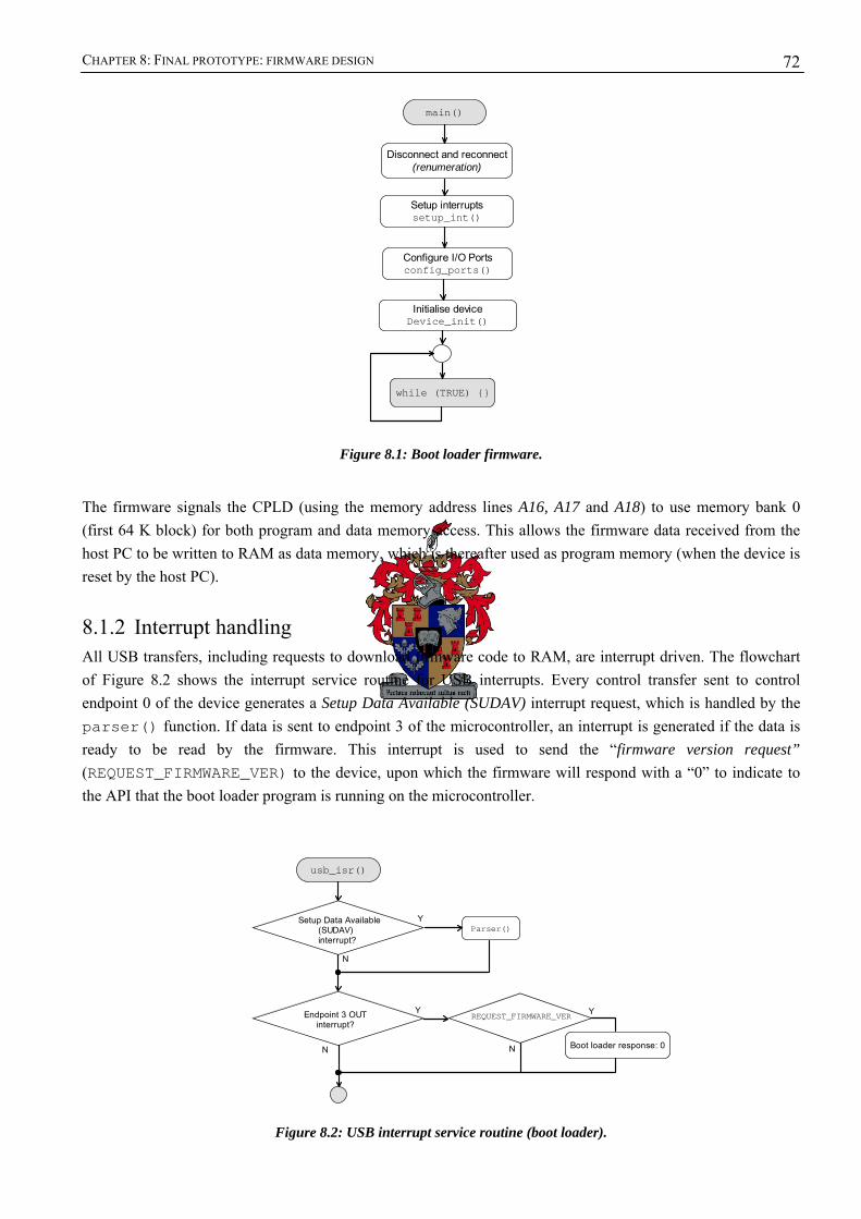
CHAPTER 8: FINAL PROTOTYPE: FIRMWARE DESIGN
72
Figure 8.1: Boot loader firmware.
The firmware signals the CPLD (using the memory address lines A16, A17 and A18) to use memory bank 0 (first 64 K block) for both program and data memory access. This allows the firmware data received from the host PC to be written to RAM as data memory, which is thereafter used as program memory (when the device is reset by the host PC).
8.1.2 Interrupt handling All USB transfers, including requests to download firmware code to RAM, are interrupt driven. The flowchart of Figure 8.2 shows the interrupt service routine for USB interrupts. Every control transfer sent to control endpoint 0 of the device generates a Setup Data Available (SUDAV) interrupt request, which is handled by the parser() function. If data is sent to endpoint 3 of the microcontroller, an interrupt is generated if the data is ready to be read by the firmware. This interrupt is used to send the “firmware version request” (REQUEST_FIRMWARE_VER) to the device, upon which the firmware will respond with a “0” to indicate to the API that the boot loader program is running on the microcontroller.
Figure 8.2: USB interrupt service routine (boot loader).
usb_isr()
Parser()
REQUEST_FIRMWARE_VER
Setup Data Available (SUDAV) interrupt?
Endpoint 3 OUT interrupt?
Y
N
N
Y
N Boot loader response: 0
Y
main()
Setup interruptssetup_int()
Configure I/O Portsconfig_ports()
Disconnect and reconnect(renumeration)
Initialise deviceDevice_init()
while (TRUE)
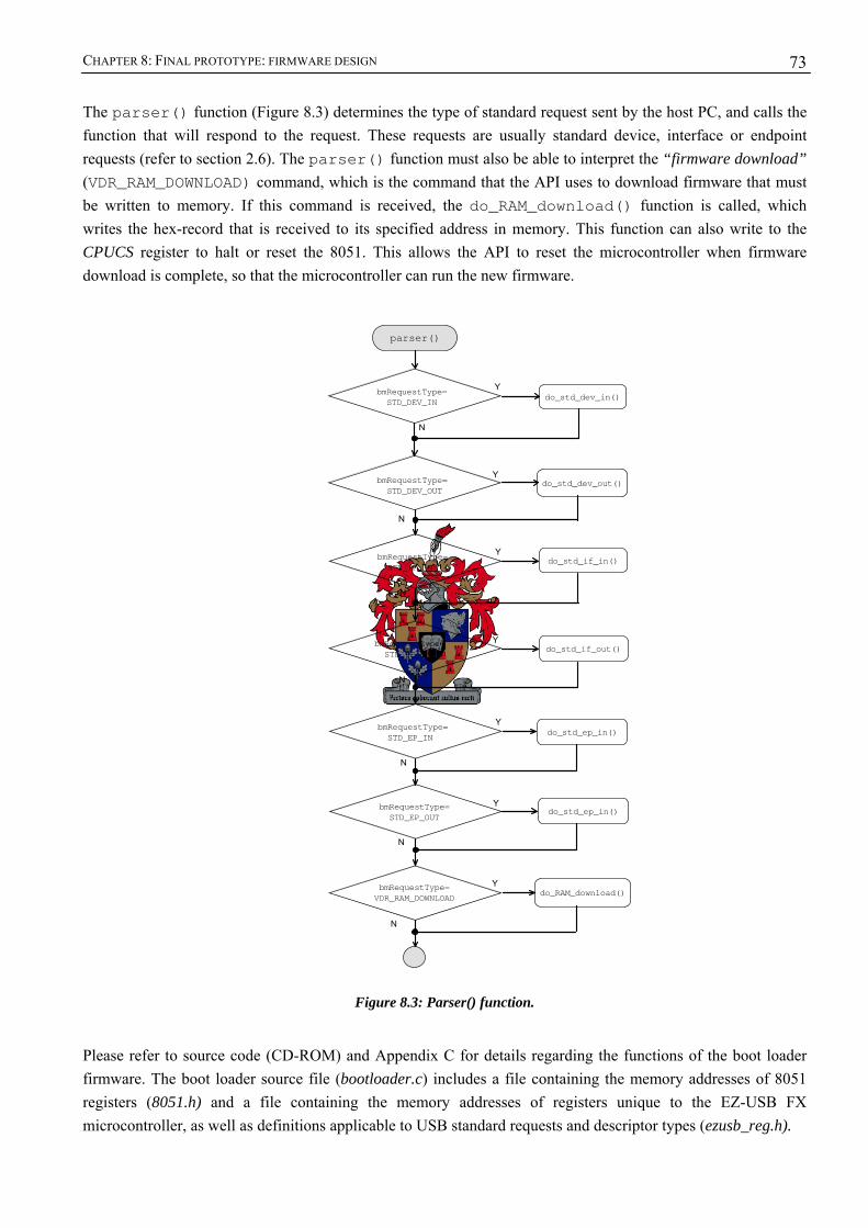
CHAPTER 8: FINAL PROTOTYPE: FIRMWARE DESIGN
73
The parser() function (Figure 8.3) determines the type of standard request sent by the host PC, and calls the function that will respond to the request. These requests are usually standard device, interface or endpoint requests (refer to section 2.6). The parser() function must also be able to interpret the “firmware download” (VDR_RAM_DOWNLOAD) command, which is the command that the API uses to download firmware that must be written to memory. If this command is received, the do_RAM_download() function is called, which writes the hex-record that is received to its specified address in memory. This function can also write to the CPUCS register to halt or reset the 8051. This allows the API to reset the microcontroller when firmware download is complete, so that the microcontroller can run the new firmware.
Figure 8.3: Parser() function.
Please refer to source code (CD-ROM) and Appendix C for details regarding the functions of the boot loader firmware. The boot loader source file (bootloader.c) includes a file containing the memory addresses of 8051 registers (8051.h) and a file containing the memory addresses of registers unique to the EZ-USB FX microcontroller, as well as definitions applicable to USB standard requests and descriptor types (ezusb_reg.h).
parser()
do_std_dev_in()bmRequestType=STD_DEV_IN
Y
N
N
YbmRequestType=STD_DEV_OUT
bmRequestType=STD_IF_IN
Y
N
N
YbmRequestType=STD_IF_OUT
bmRequestType=STD_EP_IN
Y
N
N
YbmRequestType=STD_EP_OUT
bmRequestType=VDR_RAM_DOWNLOAD
do_std_dev_out()
do_std_if_in()
do_std_if_out()
do_std_ep_in()
do_std_ep_in()
do_RAM_download()Y
N
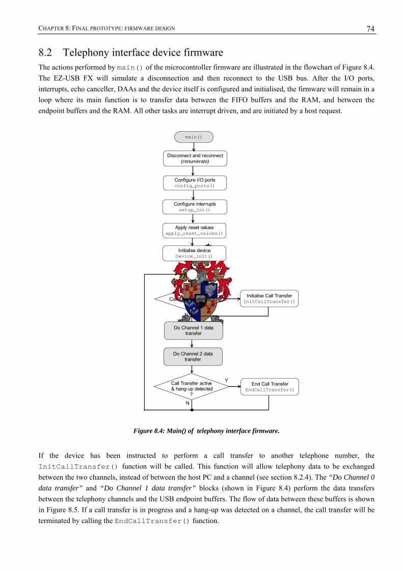
CHAPTER 8: FINAL PROTOTYPE: FIRMWARE DESIGN
74
8.2 Telephony interface device firmware The actions performed by main() of the microcontroller firmware are illustrated in the flowchart of Figure 8.4. The EZ-USB FX will simulate a disconnection and then reconnect to the USB bus. After the I/O ports, interrupts, echo canceller, DAAs and the device itself is configured and initialised, the firmware will remain in a loop where its main function is to transfer data between the FIFO buffers and the RAM, and between the endpoint buffers and the RAM. All other tasks are interrupt driven, and are initiated by a host request.
Figure 8.4: Main() of telephony interface firmware.
If the device has been instructed to perform a call transfer to another telephone number, the InitCallTransfer() function will be called. This function will allow telephony data to be exchanged between the two channels, instead of between the host PC and a channel (see section 8.2.4). The “Do Channel 0 data transfer” and “Do Channel 1 data transfer” blocks (shown in Figure 8.4) perform the data transfers between the telephony channels and the USB endpoint buffers. The flow of data between these buffers is shown in Figure 8.5. If a call transfer is in progress and a hang-up was detected on a channel, the call transfer will be terminated by calling the EndCallTransfer() function.
main()
Configure interruptssetup_int()
Apply reset valuesapply_reset_values()
Disconnect and reconnect(renumerate)
Initialise deviceDevice_init()
Do Channel 1 datatransfer
Do Channel 2 datatransfer
Call transfer started ?Initialise Call Transfer
InitCallTransfer()
Configure I/O portsconfig_ports()
Y
N
Call Transfer active& hang-up detected ?
End Call TransferEndCallTransfer()
Y
N
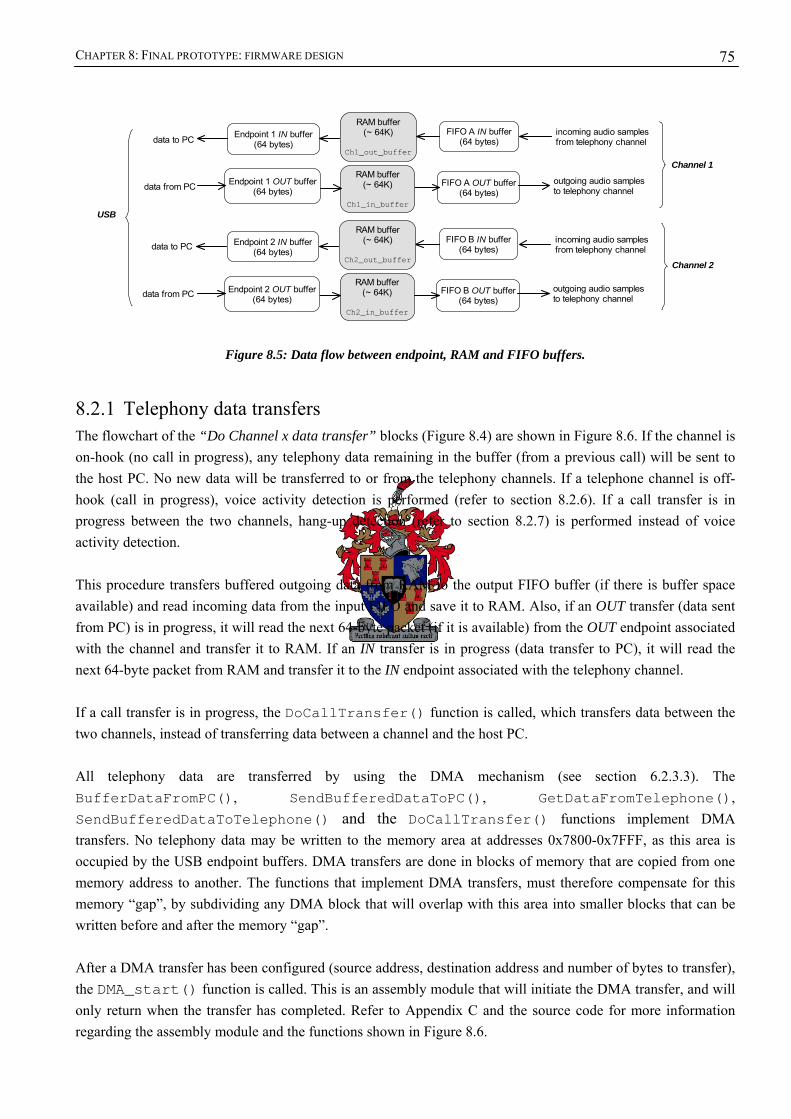
CHAPTER 8: FINAL PROTOTYPE: FIRMWARE DESIGN
75
Figure 8.5: Data flow between endpoint, RAM and FIFO buffers.
8.2.1 Telephony data transfers The flowchart of the “Do Channel x data transfer” blocks (Figure 8.4) are shown in Figure 8.6. If the channel is on-hook (no call in progress), any telephony data remaining in the buffer (from a previous call) will be sent to the host PC. No new data will be transferred to or from the telephony channels. If a telephone channel is off-hook (call in progress), voice activity detection is performed (refer to section 8.2.6). If a call transfer is in progress between the two channels, hang-up detection (refer to section 8.2.7) is performed instead of voice activity detection. This procedure transfers buffered outgoing data from RAM to the output FIFO buffer (if there is buffer space available) and read incoming data from the input FIFO and save it to RAM. Also, if an OUT transfer (data sent from PC) is in progress, it will read the next 64-byte packet (if it is available) from the OUT endpoint associated with the channel and transfer it to RAM. If an IN transfer is in progress (data transfer to PC), it will read the next 64-byte packet from RAM and transfer it to the IN endpoint associated with the telephony channel. If a call transfer is in progress, the DoCallTransfer() function is called, which transfers data between the two channels, instead of transferring data between a channel and the host PC. All telephony data are transferred by using the DMA mechanism (see section 6.2.3.3). The BufferDataFromPC(), SendBufferedDataToPC(), GetDataFromTelephone(), SendBufferedDataToTelephone() and the DoCallTransfer() functions implement DMA transfers. No telephony data may be written to the memory area at addresses 0x7800-0x7FFF, as this area is occupied by the USB endpoint buffers. DMA transfers are done in blocks of memory that are copied from one memory address to another. The functions that implement DMA transfers, must therefore compensate for this memory “gap”, by subdividing any DMA block that will overlap with this area into smaller blocks that can be written before and after the memory “gap”. After a DMA transfer has been configured (source address, destination address and number of bytes to transfer), the DMA_start() function is called. This is an assembly module that will initiate the DMA transfer, and will only return when the transfer has completed. Refer to Appendix C and the source code for more information regarding the assembly module and the functions shown in Figure 8.6.
FIFO A IN buffer(64 bytes)
RAM buffer(~ 64K)
Ch1_out_buffer
Endpoint 1 IN buffer(64 bytes)
FIFO A OUT buffer(64 bytes)
RAM buffer(~ 64K)
Ch1_in_buffer
Endpoint 1 OUT buffer(64 bytes)
data to PC
data from PC
incoming audio samplesfrom telephony channel
outgoing audio samplesto telephony channel
FIFO B IN buffer(64 bytes)
RAM buffer(~ 64K)
Ch2_out_buffer
Endpoint 2 IN buffer(64 bytes)
FIFO B OUT buffer(64 bytes)
RAM buffer(~ 64K)
Ch2_in_buffer
Endpoint 2 OUT buffer(64 bytes)
data to PC
data from PC
incoming audio samplesfrom telephony channel
outgoing audio samplesto telephony channel
Channel 1
Channel 2
USB
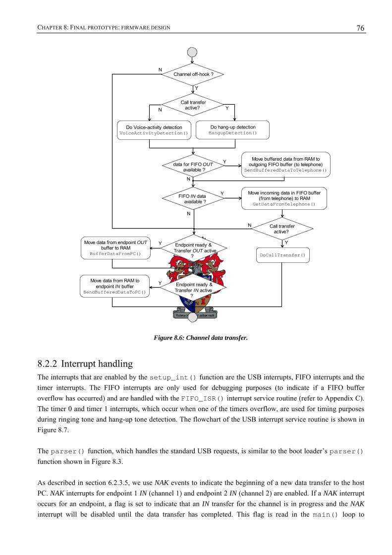
CHAPTER 8: FINAL PROTOTYPE: FIRMWARE DESIGN
76
Y
N
Y
N
Do Voice-activity detectionVoiceActivityDetection()
Move buffered data from RAM tooutgoing FIFO buffer (to telephone)
SendBufferedDataToTelephone()
Move incoming data in FIFO buffer(from telephone) to RAM
GetDataFromTelephone()
Y
N
Move data from endpoint OUTbuffer to RAM
BufferDataFromPC()
Move data from RAM toendpoint IN buffer
SendBufferedDataToPC()
Y
N
Y
N
Channel off-hook ?
data for FIFO OUT available ?
FIFO IN data available ?
Endpoint ready &Transfer OUT active ?
Endpoint ready &Transfer IN active ?
Call transfer active?
DoCallTransfer()
N
Y
Call transfer active?
Do hang-up detectionHangupDetection()
YN
Figure 8.6: Channel data transfer.
8.2.2 Interrupt handling The interrupts that are enabled by the setup_int() function are the USB interrupts, FIFO interrupts and the timer interrupts. The FIFO interrupts are only used for debugging purposes (to indicate if a FIFO buffer overflow has occurred) and are handled with the FIFO_ISR() interrupt service routine (refer to Appendix C). The timer 0 and timer 1 interrupts, which occur when one of the timers overflow, are used for timing purposes during ringing tone and hang-up tone detection. The flowchart of the USB interrupt service routine is shown in Figure 8.7. The parser() function, which handles the standard USB requests, is similar to the boot loader’s parser() function shown in Figure 8.3. As described in section 6.2.3.5, we use NAK events to indicate the beginning of a new data transfer to the host PC. NAK interrupts for endpoint 1 IN (channel 1) and endpoint 2 IN (channel 2) are enabled. If a NAK interrupt occurs for an endpoint, a flag is set to indicate that an IN transfer for the channel is in progress and the NAK interrupt will be disabled until the data transfer has completed. This flag is read in the main() loop to

CHAPTER 8: FINAL PROTOTYPE: FIRMWARE DESIGN
77
determine if the SendBufferedData() function must be called, which will transfer data to the IN endpoint buffer associated with the channel. In the same manner, OUT transfers (transfers from the host PC) are initiated by an OUT interrupt for endpoint 1 (channel 1) or endpoint 2 (channel 2). The USB interrupt service routine will set a flag to indicate that an OUT transfer for the channel is in progress and future OUT interrupts for the endpoint will be disabled until the data transfer has completed. This flag is read in the main() loop to determine if the BufferDataFromPC() function must be called, which will transfer the received data from the OUT endpoint to the RAM buffer.
Figure 8.7: USB interrupt service routine.
Commands or requests relating to the telephony channels, such as answering calls, placing a channel on-hook, requesting the size of buffers etc. are sent to endpoint 3. If an OUT interrupt occurs for endpoint 3, the ChannelCommand() function is called to respond to the command or request. There are 36 commands that this function must be able to interpret (refer to the source code for details). The interrupt vector table is written in assembly (ivect.asm), and is compiled as a separate module. This module is then linked to the main firmware project and is placed at address 0x0000 in memory. Refer to Appendix C for details.
usb_isr()
Parser()Setup Data Available (SUDAV) interrupt?
Endpoint 1 IN NAK interrupt?
Y
N
N
YDisable endpoint 1 NAK interruptCh1_in_transfer = TRUE
Endpoint 2 IN NAK interrupt?
N
YDisable endpoint 2 NAK interruptCh2_in_transfer = TRUE
Endpoint 1 OUT interrupt?
N
Y Disable endpoint 1 OUT interruptCh1_out_transfer = TRUE
Endpoint 2 OUT interrupt?
N
YDisable endpoint 2 OUT interruptCh2_out_transfer = TRUE
ChannelCommand()Endpoint 3 OUT interrupt?
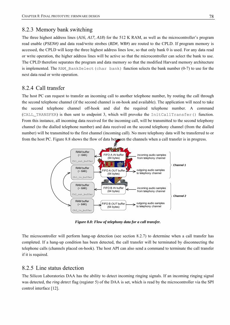
CHAPTER 8: FINAL PROTOTYPE: FIRMWARE DESIGN
78
8.2.3 Memory bank switching The three highest address lines (A16, A17, A18) for the 512 K RAM, as well as the microcontroller’s program read enable (PSEN#) and data read/write strobes (RD#, WR#) are routed to the CPLD. If program memory is accessed, the CPLD will keep the three highest address lines low, so that only bank 0 is used. For any data read or write operation, the higher address lines will be active so that the microcontroller can select the bank to use. The CPLD therefore separates the program and data memory so that the modified Harvard memory architecture is implemented. The RAM_BankSelect(char bank) function selects the bank number (0-7) to use for the next data read or write operation.
8.2.4 Call transfer The host PC can request to transfer an incoming call to another telephone number, by routing the call through the second telephone channel (if the second channel is on-hook and available). The application will need to take the second telephone channel off-hook and dial the required telephone number. A command (CALL_TRANSFER) is then sent to endpoint 3, which will provoke the InitCallTransfer() function. From this instance, all incoming data received for the incoming call, will be transmitted to the second telephony channel (to the dialled telephone number) and data received on the second telephony channel (from the dialled number) will be transmitted to the first channel (incoming call). No more telephony data will be transferred to or from the host PC. Figure 8.8 shows the flow of data between the channels when a call transfer is in progress.
FIFO A IN buffer(64 bytes)
RAM buffer(~ 64K)
Ch1_out_buffer
FIFO A OUT buffer(64 bytes)
RAM buffer(~ 64K)
Ch1_in_buffer
incoming audio samplesfrom telephony channel
outgoing audio samplesto telephony channel
FIFO B IN buffer(64 bytes)
RAM buffer(~ 64K)
Ch2_out_buffer
FIFO B OUT buffer(64 bytes)
RAM buffer(~ 64K)
Ch2_in_buffer
incoming audio samplesfrom telephony channel
outgoing audio samplesto telephony channel
Channel 1
Channel 2
Figure 8.8: Flow of telephony data for a call transfer.
The microcontroller will perform hang-up detection (see section 8.2.7) to determine when a call transfer has completed. If a hang-up condition has been detected, the call transfer will be terminated by disconnecting the telephone calls (channels placed on-hook). The host API can also send a command to terminate the call transfer if it is required.
8.2.5 Line status detection The Silicon Laboratories DAA has the ability to detect incoming ringing signals. If an incoming ringing signal was detected, the ring detect flag (register 5) of the DAA is set, which is read by the microcontroller via the SPI control interface [12].
CHAPTER 8: FINAL PROTOTYPE: FIRMWARE DESIGN
79
A ringing signal is defined if a voltage greater than the positive ring threshold, or if a voltage less than the negative ring threshold is detected on the line. If a ringing signal is detected (positive or negative), the ring detect flag will be set. The threshold values can be adjusted by writing new values to the threshold registers of the DAA. Invalid ringing signals could be detected if line-voltage changes occur due to pulse dialling, line tests or a parallel handset going off-hook. The DAA can perform additional ring validation which prevents false triggering of the ring detection circuitry. This is done by validating ring parameters, which is programmed in a series of control registers. The ring validation circuit calculates the time between alternating crossings of the positive and negative ringing signal. The ringing signal must be validated within a high and low frequency tolerance for a certain time interval (register 23). The high and low frequency tolerances are programmed to register 22 and 24 respectively. Once the signal has been validated for this time interval, the circuitry begins to check for the end of the ring signal, which is defined as the lack of additional threshold crossing for a specified time interval (register 23). If the DAA’s ring validation feature is enabled, the ring detect flag will only indicate a ringing signal that has been validated by these parameters. As soon as the microcontroller detected that the ring detect flag is set, it will report the channel status as “RINGING” and it will start a timer. If no new ring signals are detected before the timer has expired, the channel status is reset to “ON-HOOK”. If a large negative line voltage (approximately –45 V DC) is measured by the DAA, it is assumed that the telephone line is properly connected to the device and the channel status will be reported as “ON-HOOK”. If the line voltage is measured to be 0 V, there is an error with the telephone line connection and the line status will be changed to “NO-LINE”. If a channel is taken off-hook by issuing the DAA with an off-hook command, the line status will be changed to “OFF-HOOK” until an on-hook command is received.
8.2.6 Voice activity detection The state diagram of the Voice Activity Detector (VAD), implemented with the VoiceActivityDetection(Byte channel) function, is shown in Figure 8.9. The voice activity detection algorithm will only execute if the “barge-in” or “record on voice activity” feature is enabled via the API. The echo canceller’s double-talk flag is continuously polled to determine if there is any caller speech present in the incoming signal (state 1). If the flag is active, the VAD algorithm is activated (state 2). The VAD algorithm measures the energy and zero-crossing rate of the incoming signal, as described in section 6.3.5.1. If a sufficient number of frames are measured above the energy and ZCR threshold values, speech is indicated. If the energy and ZCR measurements indicate that there is no speech present, the voice activity detection algorithm returns to the idle state (state 1). If speech is detected (state 3) and the “record on voice activity” feature is enabled, the microcontroller will start recording incoming speech data. If barge-in is enabled, a barge-in condition will also be indicated. As long as caller speech is present in the incoming signal (indicated by the energy and ZCR measurements), the VAD will remain in state 3. A timer is activated, which is reset every time that voice activity is detected. The VAD enters state 4 as soon as the timer reached a threshold value (no speech present for PostSpeechTimeout seconds). This state indicates that the end of an utterance was detected, and it will remain in this state until the RESET_VAD command from the API was received. All the parameters used during voice activity detection (threshold values, timeout values etc.) can be adjusted via the API (refer to Chapter 9).

CHAPTER 8: FINAL PROTOTYPE: FIRMWARE DESIGN
80
Idle Measure Energy & ZCR
Barge-in detectedVoice-activity detectedEnd of utterance detected
Double-talk detection Voice-activity detection
Double-talk detect / activate VAD
Silence detect / de-activate VAD
Run timer if no voice-activity detected Voice- activity detected /
Reset timer
timer > PostSpeechTimeout
VoiceActivityDetection(Byte Channel)
Reset VAD
Wait for reset
Voice- activity detected /Record incoming speech
1 2
34
Figure 8.9: Voice activity detector state diagram.
8.2.7 Hang-up detection During a call transfer, hang-up detection is performed to determine when the call has finished. This is required so that the DAAs can place the channels back on-hook to allow a new incoming call. If a caller has hung-up, the PBX or central office (CO) equipment will generate a hang-up tone for a few seconds. Hang-up tone detection is performed, which is similar to voice activity detection (section 8.2.6) but with some additional constraints. A hang-up tone is detected if the measured ZCR and energy falls within minimum and maximum threshold values for a specified time interval. To determine the default minimum and maximum threshold values, the hang-up tone was recorded and, by using Matlab, the energy and ZCR were measured. The hang-up tone parameters (threshold values, time interval) can be adjusted via the API. Unfortunately, the ringing tone that is received from the dialled telephone number has the same frequency as the hang-up tone. The two signals are only differentiated by their cadencies (on-time and off-time). The EZ-USB FX has limited computational capabilities, and cannot perform the signal processing required to distinguish between the two signals. We can therefore only perform hang-up tone detection on the caller’s incoming signal, and not on the incoming signal of the dialled telephone number (which contains a ringing signal until the telephone is answered). If hang-up tone detection should fail for any reason, we would still be able to detect a hang-up condition. The microcontroller will automatically assume that a call transfer has ended if there is no more speech activity for “NoSpeechTimeout” seconds on both channels. This is determined by activating a timer, which is reset every time that voice activity is detected on either channel. If the timer reaches a threshold value, the end of the call transfer is assumed and both channels are placed back on-hook.
8.3 Altera CPLD design The Altera CPLD performs the following functions:
• Memory bank switching and control of the 512 K RAM. • Generation of PCM timing signals for the DAAs and the echo canceller (PCM highway clock signal and
frame signals).
CHAPTER 8: FINAL PROTOTYPE: FIRMWARE DESIGN
81
• Generation of PCM timeslot enable strobes for the echo canceller. • Generation of read, write and control signals for the slave FIFO buffers of the microcontroller. • Interfacing of the PCM transmit and receive signals to the microcontroller.
8.3.1 Bank switching and RAM control Figure 8.10 shows the schematic GDF (graphical design file) entry for the bank switching and RAM control logic.
Figure 8.10: Memory bank switching and RAM control logic schematic. The EZ-USB FX microcontroller has a 16-bit address bus, and can thus only access 64K of external RAM directly. Three I/O pins of the microcontroller are used to provide additional “address lines”, which allows us to divide the 512 K RAM into eight 64 K banks. The RAM_Bank_select block is a graphical symbol for an entity ([39], p. 37), and its function is defined by the following VHDL code segment: library ieee; use ieee.std_logic_1164.all, ieee.std_logic_unsigned.all; entity ram_bank_select is port(clkin : in std_logic; PSENn : in std_logic; A16 : in std_logic; A17 : in std_logic; A18
: in std_logic; RAM_A16 : out std_logic; RAM_A17: out std_logic; RAM_A18 : out std_logic); end entity ram_bank_select; architecture ram_bank of ram_bank_select is begin process (clkin) is variable counter : integer := 126; begin if rising_edge(clkin) then if (PSENn='0') then RAM_A16 <= '0'; RAM_A17 <= '0'; RAM_A18 <= '0'; else RAM_A16 <= A16; RAM_A17 <= A17; RAM_A18 <= A18; end if; end if; end process; end architecture ram_bank;
The code inside the “architecture” block is a process which only executes when the 48 MHz clock signal from the microcontroller (clkin), changes. When a rising edge of the clock signal is detected, the code in the “begin-end process” block will be executed. If the PSEN signal is active, the code will force the output address lines (RAM_A16-RAM_A18) to 0, otherwise the input address signals are directly routed to the output signals. The PSEN signal is active when code is read, thus code will always be fetched from bank 0. The other
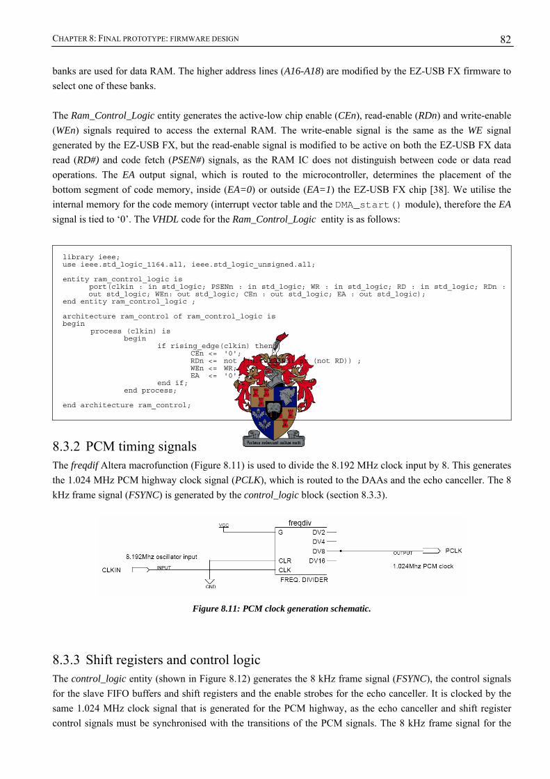
CHAPTER 8: FINAL PROTOTYPE: FIRMWARE DESIGN
82
banks are used for data RAM. The higher address lines (A16-A18) are modified by the EZ-USB FX firmware to select one of these banks. The Ram_Control_Logic entity generates the active-low chip enable (CEn), read-enable (RDn) and write-enable (WEn) signals required to access the external RAM. The write-enable signal is the same as the WE signal generated by the EZ-USB FX, but the read-enable signal is modified to be active on both the EZ-USB FX data read (RD#) and code fetch (PSEN#) signals, as the RAM IC does not distinguish between code or data read operations. The EA output signal, which is routed to the microcontroller, determines the placement of the bottom segment of code memory, inside (EA=0) or outside (EA=1) the EZ-USB FX chip [38]. We utilise the internal memory for the code memory (interrupt vector table and the DMA_start() module), therefore the EA signal is tied to ‘0’. The VHDL code for the Ram_Control_Logic entity is as follows:
8.3.2 PCM timing signals The freqdif Altera macrofunction (Figure 8.11) is used to divide the 8.192 MHz clock input by 8. This generates the 1.024 MHz PCM highway clock signal (PCLK), which is routed to the DAAs and the echo canceller. The 8 kHz frame signal (FSYNC) is generated by the control_logic block (section 8.3.3).
Figure 8.11: PCM clock generation schematic.
8.3.3 Shift registers and control logic The control_logic entity (shown in Figure 8.12) generates the 8 kHz frame signal (FSYNC), the control signals for the slave FIFO buffers and shift registers and the enable strobes for the echo canceller. It is clocked by the same 1.024 MHz clock signal that is generated for the PCM highway, as the echo canceller and shift register control signals must be synchronised with the transitions of the PCM signals. The 8 kHz frame signal for the
library ieee; use ieee.std_logic_1164.all, ieee.std_logic_unsigned.all; entity ram_control_logic is port(clkin : in std_logic; PSENn : in std_logic; WR : in std_logic; RD : in std_logic; RDn :
out std_logic; WEn: out std_logic; CEn : out std_logic; EA : out std_logic); end entity ram_control_logic ; architecture ram_control of ram_control_logic is begin process (clkin) is begin if rising_edge(clkin) then CEn <= '0'; RDn <= not ((not PSENn) or (not RD)) ; WEn <= WR; EA <= '0'; end if; end process; end architecture ram_control;
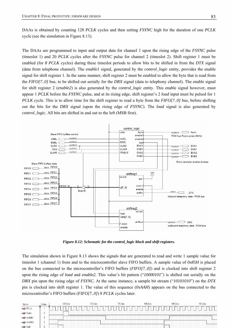
CHAPTER 8: FINAL PROTOTYPE: FIRMWARE DESIGN
83
DAAs is obtained by counting 128 PCLK cycles and then setting FSYNC high for the duration of one PCLK cycle (see the simulation in Figure 8.13).
The DAAs are programmed to input and output data for channel 1 upon the rising edge of the FSYNC pulse (timeslot 1) and 20 PCLK cycles after the FSYNC pulse for channel 2 (timeslot 2). Shift register 1 must be enabled (for 8 PCLK cycles) during these timeslot periods to allow bits to be shifted in from the DTX signal (data from telephone channel). The enable1 signal, generated by the control_logic entity, provides the enable signal for shift register 1. In the same manner, shift register 2 must be enabled to allow the byte that is read from the FIFO[7..0] bus, to be shifted out serially for the DRX signal (data to telephony channel). The enable signal for shift register 2 (enable2) is also generated by the control_logic entity. This enable signal however, must appear 1 PCLK before the FSYNC pulse, and at its rising edge, shift register’s 2 load input must be pulsed for 1 PCLK cycle. This is to allow time for the shift register to read a byte from the FIFO[7..0] bus, before shifting out the bits for the DRX signal (upon the rising edge of FSYNC). The load signal is also generated by control_logic. All bits are shifted in and out to the left (MSB first).
Figure 8.12: Schematic for the control_logic block and shift registers.
The simulation shown in Figure 8.13 shows the signals that are generated to read and write 1 sample value for timeslot 1 (channel 1) from and to the microcontroller slave FIFO buffers. A sample value of 0x85H is placed on the bus connected to the microcontroller’s FIFO buffers (FIFO[7..0]) and is clocked into shift register 2 upon the rising edge of load and enable2. This value’s bit pattern (“10000101”) is shifted out serially on the DRX pin upon the rising edge of FSYNC. At the same instance, a sample bit stream (“10101010”) on the DTX pin is clocked into shift register 1. The value of this sequence (0xAAH) appears on the bus connected to the microcontroller’s FIFO buffers (FIFO[7..0]) 8 PCLK cycles later.
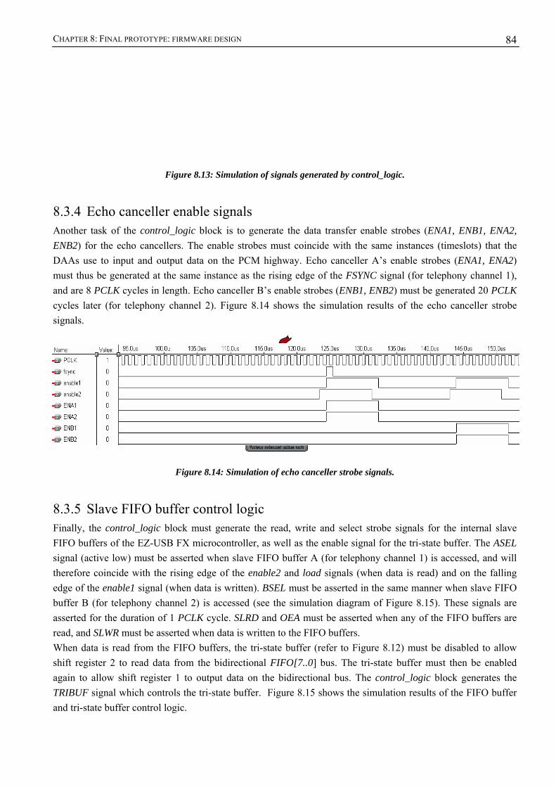
CHAPTER 8: FINAL PROTOTYPE: FIRMWARE DESIGN
84
Figure 8.13: Simulation of signals generated by control_logic.
8.3.4 Echo canceller enable signals Another task of the control_logic block is to generate the data transfer enable strobes (ENA1, ENB1, ENA2, ENB2) for the echo cancellers. The enable strobes must coincide with the same instances (timeslots) that the DAAs use to input and output data on the PCM highway. Echo canceller A’s enable strobes (ENA1, ENA2) must thus be generated at the same instance as the rising edge of the FSYNC signal (for telephony channel 1), and are 8 PCLK cycles in length. Echo canceller B’s enable strobes (ENB1, ENB2) must be generated 20 PCLK cycles later (for telephony channel 2). Figure 8.14 shows the simulation results of the echo canceller strobe signals.
Figure 8.14: Simulation of echo canceller strobe signals.
8.3.5 Slave FIFO buffer control logic Finally, the control_logic block must generate the read, write and select strobe signals for the internal slave FIFO buffers of the EZ-USB FX microcontroller, as well as the enable signal for the tri-state buffer. The ASEL signal (active low) must be asserted when slave FIFO buffer A (for telephony channel 1) is accessed, and will therefore coincide with the rising edge of the enable2 and load signals (when data is read) and on the falling edge of the enable1 signal (when data is written). BSEL must be asserted in the same manner when slave FIFO buffer B (for telephony channel 2) is accessed (see the simulation diagram of Figure 8.15). These signals are asserted for the duration of 1 PCLK cycle. SLRD and OEA must be asserted when any of the FIFO buffers are read, and SLWR must be asserted when data is written to the FIFO buffers. When data is read from the FIFO buffers, the tri-state buffer (refer to Figure 8.12) must be disabled to allow shift register 2 to read data from the bidirectional FIFO[7..0] bus. The tri-state buffer must then be enabled again to allow shift register 1 to output data on the bidirectional bus. The control_logic block generates the TRIBUF signal which controls the tri-state buffer. Figure 8.15 shows the simulation results of the FIFO buffer and tri-state buffer control logic.
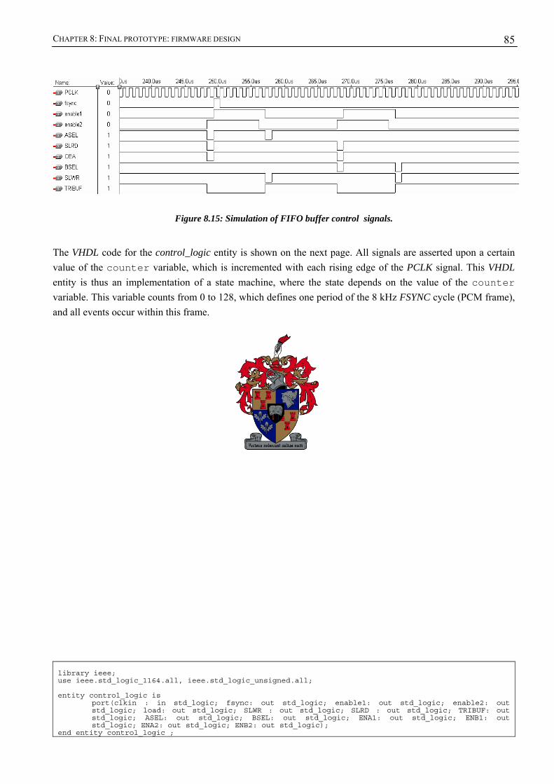
CHAPTER 8: FINAL PROTOTYPE: FIRMWARE DESIGN
85
Figure 8.15: Simulation of FIFO buffer control signals.
The VHDL code for the control_logic entity is shown on the next page. All signals are asserted upon a certain value of the counter variable, which is incremented with each rising edge of the PCLK signal. This VHDL entity is thus an implementation of a state machine, where the state depends on the value of the counter variable. This variable counts from 0 to 128, which defines one period of the 8 kHz FSYNC cycle (PCM frame), and all events occur within this frame. library ieee; use ieee.std_logic_1164.all, ieee.std_logic_unsigned.all; entity control_logic is port(clkin : in std_logic; fsync: out std_logic; enable1: out std_logic; enable2: out
std_logic; load: out std_logic; SLWR : out std_logic; SLRD : out std_logic; TRIBUF: out std_logic; ASEL: out std_logic; BSEL: out std_logic; ENA1: out std_logic; ENB1: out std_logic; ENA2: out std_logic; ENB2: out std_logic);
end entity control_logic ;
CHAPTER 8: FINAL PROTOTYPE: FIRMWARE DESIGN
86
architecture generator of control_logic is constant Slot2: integer:= 20; constant Slot1: integer:= 0; begin process (clkin) is variable counter : integer := 126; begin if rising_edge(clkin) then counter := counter+1; SLWR <= '1'; SLRD <= '1'; fsync <= '0'; ASEL <= '1'; BSEL <= '1'; if (counter=Slot1+7) then enable2 <= '0'; end if; if (counter=Slot1+8) then enable1 <= '0'; SLWR <= '0'; ASEL <= '0'; TRIBUF <= '1'; ENA1 <= '0'; ENA2 <= '0'; end if; if (counter=Slot2-1) then enable2 <= '1'; load <= '1'; SLRD <= '0'; BSEL <= '0'; TRIBUF <= '0'; end if; if (counter=Slot2) then ENB1 <= '1'; ENB2 <= '1'; enable1<= '1'; load <= '0'; end if; if (counter=Slot2+7) then enable2 <= '0'; end if; if (counter=Slot2+8) then enable1 <= '0'; SLWR <= '0'; BSEL <= '0'; TRIBUF <= '1'; ENB1 <= '0'; ENB2 <= '0'; end if; if (counter=127) then --slot1-1 enable2 <= '1'; load <= '1'; SLRD <= '0'; ASEL <= '0'; TRIBUF <= '0'; end if; if (counter=128) then --slot1 counter:=0; fsync <= '1'; enable1 <= '1'; load <= '0'; ENA1 <= '1'; ENA2 <= '1'; end if; end if; end process; end architecture generator;
Chapter 9
9. API design
API design The application programming interface (API) is a collection of functions, developed using the open-source, platform-independent USB library, LibUSB (refer to section 3.4 for the LibUSB API). The API can be compiled under both Microsoft Windows and Linux operating systems. This chapter describes the functions available in the API. Refer to the source code on the CD-ROM for more details.
9.1 Initialisation functions This section describes the functions relating to the opening, initialisation and closing of the hardware device.
9.1.1 InitTID Prototype: int InitTID(Byte Verbose)
This function searches for the USB telephony interface device on the USB bus. If the device is found, it initialises the device for use. This function must be called before any of the other functions of the API may be called.
Inputs: Verbose – Use “1” to display and “0” to hide tracing information. Outputs: Integer – Code indicating device status. 0 = No USB telephony interface device found on USB bus.
1 = Device found, but the boot loader is waiting for the telephony interface firmware to be downloaded. Use the DownloadTIDfirmware() function. 2 = The USB telephony interface device is found on the bus and ready for use.
9.1.2 DownloadTIDfirmware Prototype: int DownloadTIDfirmware(BYTE verbose, void UpdProgress)(int,char))
This function downloads the telephony interface device firmware to the device running the boot loader program. Use the InitTID() function first to test if the boot loader firmware is running. After the download is completed, the device is initialised and ready for use (InitTID() need not be called again).
Inputs: verbose – Use “1” to display trace information and “0” to hide. *UpdProgress – Function pointer to a callback function (optional). The user must provide this optional callback function, which is called during the download process. It can be used, for example, to update a download progress display. Use NULL if the callback function is not required. The first parameter of the callback function is an integer, indicating the percentage of the download
CHAPTER 9: API DESIGN
88
process completed, and the second parameter (char) is the same verbose parameter that is passed to this function.
Outputs: Integer – Code indicating if download process was a success. 0 = Success, telephony interface firmware running. 1 = Failure.
9.1.3 TestTID Prototype: int TestTID(BYTE verbose)
This function tests the communication interface between components on the hardware device.
Inputs: verbose – “1” will output the results of the tests and “0” will hide this information. Outputs: Integer - Indicates the result of the test.
0 = No problems detected. 1 = Communications failure between one or more hardware components.
9.1.4 CloseTID Prototype: int CloseTID()
This function will release the handle on the USB telephony interface device.
Inputs: None. Outputs: Integer – Indicates success or failure.
0 = Device successfully closed. 1 = Problem closing device (probably already closed, or never initialised).
9.2 Buffer-related functions This section describes the functions relating to the management of the buffers used for the incoming and outgoing telephony data, as well as the sending and receiving of the buffer data.
9.2.1 CreateTelephonyBuffer Prototype: TelephonyBuffer *CreateTelephonyBuffer(int iChannel)
This function creates a new buffer in memory (of the TelephonyBuffer type) to use for incoming and outgoing telephony data, and assigns this buffer to a specific telephony channel (channel 1 or channel 2) of the hardware device. The function returns a pointer to the new telephony buffer in memory. Many of the functions in this API require a pointer to a telephony buffer, and this pointer must point to a valid buffer, which is created and initialised by this function. The buffers in the TelephonyBuffer structure that are used for the incoming and outgoing audio data, are based on the Audio_Buffer type, from Dr. T.R. Niesler (please refer to the “audio.incl.c” file in the source code).
Inputs: iChannel – The channel number to assign to this buffer (1 or 2). Outputs: A pointer to the new buffer in memory.
9.2.2 DeleteTelephonyBuffer Prototype: void DeleteTelephonyBuffer(TelephonyBuffer *TheBuffer)
CHAPTER 9: API DESIGN
89
This function deletes a telephony buffer that is no longer required (to free memory).
Inputs: *TheBuffer – The buffer to be deleted. Outputs: None.
9.2.3 ClearTelephonyBuffer Prototype: void ClearTelephonyBuffer(TelephonyBuffer *TheBuffer)
This functions clears the argument telephony buffer of all incoming and outgoing telephony data. This function is rarely required by an application. Instead, other API functions use this function when the telephony buffer must be cleared.
Inputs: *TheBuffer – The buffer to be cleared. Outputs: None.
9.2.4 GetTelephonyHardwareBufferSize Prototype: long GetTelephonyHardwareBufferSize(TelephonyBuffer *TheBuffer)
This function retrieves the current size of the hardware buffer that is used to store outgoing telephony data. This function is used by the API’s SendTelephonyBufferData() function to determine how much data can be sent to the device to be buffered, and is usually not used by an application. If it is used however, care must be taken to limit the frequency at which this function is called, as this function sends a USB request to the device. If too many requests are received, the device’s performance will be affected. Do not place this function inside a loop.
Inputs: *TheBuffer – The buffer (and associated channel) of which the size must be retrieved. Outputs: Long – The current size in bytes of the outgoing hardware buffer for the channel specified in
TheBuffer.
9.2.5 SendTelephonyBufferData Prototype: long SendTelephonyBufferData(TelephonyBuffer *TheBuffer, long
nBytes);
This function will send the number of bytes specified (which is stored in the outgoing channel buffer) to the device. It must be called at a high enough frequency to ensure that the user receives an uninterrupted audio signal. The channel must be off-hook before this function can be called. The hardware buffer space that is available is determined, and if the buffer can accommodate the requested number of bytes, it will be transferred to the device (up to a maximum of 8000 bytes per transfer). The function returns with the actual number of bytes that was sent to the device. The total number of bytes sent since the last time that the outgoing buffer was loaded with new data, is indicated by the Bytes_sent field of the telephony buffer. Time stamping is performed to prevent this function from sending too many USB requests to the device. If the function is called before the time interval specified for this function has expired, it would return with zero as the number of bytes sent. Also, if a call transfer is in progress, this function will have no effect, and would also return with zero as the number of bytes sent.
Inputs: *TheBuffer - The buffer (and associated channel) to which the data will be sent. nBytes – The number of bytes that must be sent to the device.
CHAPTER 9: API DESIGN
90
Outputs: Long – The number of bytes that was successfully sent to the device.
9.2.6 FlushTelephonyBuffer Prototype: long FlushTelephonyBuffer(TelephonyBuffer *TheBuffer)
This function uses the SendTelephonyBufferData() function to send all the available data in the outgoing buffer, and would only return once all the data is sent. This function is usually not used from an application, as it could take long to complete if there are a large number of samples stored in the outgoing buffer. This time delay could cause the incoming hardware buffer to overflow, since the FetchAllTelephonyBufferData() function is not called while this function is executing. It is used by other API functions to send DTMF tones to the device.
Inputs: *TheBuffer – The buffer (and associated channel) to which the data will be sent. Outputs: Long – The number of bytes that was successfully sent to the device.
9.2.7 FetchAllTelephonyBufferData Prototype: long FetchAllTelephonyBufferData(TelephonyBuffer *TheBuffer)
This function will retrieve all the available incoming data that is buffered on the hardware device. It must be called often enough to avoid buffer overflow and the loss of inbound data. The channel must be off-hook before this function can be called. The function will request 8000 bytes for each transfer, but less will be transferred if less is available in the hardware buffer. The function will return with the number of samples read from the buffer. Time stamping is performed to prevent this function from sending too many USB requests to the device. If this function is called within a specified time interval, it returns zero as the number of bytes received from the device. Also, if a call transfer is in progress, this function will have no effect and returns zero as the number of bytes received.
Inputs: *TheBuffer - The buffer whose data must be fetched. Outputs: Long – The number of bytes successfully retrieved from the device.
9.2.8 TelephonyBufferDataFinishedPlaying Prototype: BOOLEAN TelephonyBufferDataFinishedPlaying(TelephonyBuffer
*TheBuffer)
This function will determine if all the outgoing telephony buffer data has been sent to the device and if the hardware device has finished playing all buffered data (buffer empty). This function is used by other API functions to confirm that all the telephony data is sent on the telephone line before continuing to the next event, for example, such as dialling DTMF tones or before disconnecting a call (putting the channel on-hook). Time stamping is performed to prevent this function from sending too many USB requests to the device. If the function is called within a specified time interval, it returns with the same status as the previous call to this function (unless new outgoing telephony data has been loaded into the buffer).
Inputs: *TheBuffer - The buffer associated with the channel to query. Outputs: BOOLEAN – Indicating whether or not a prompt has finished playing (all data transmitted on the
telephone channel). 0 (FALSE) – Still busy sending outgoing telephony data. 1 (TRUE) – All data has been sent to the telephone channel and device finished playing the data.
CHAPTER 9: API DESIGN
91
9.3 Telephony functions This section describes the API functions relating to the telephone channel operations (answering calls, hang-up etc.).
9.3.1 AnswerTelephoneCall Prototype: int AnswerTelephoneCall(TelephonyBuffer *TheBuffer)
This function answers an incoming call by taking the channel off-hook. The buffer will be cleared of all data, therefore existing buffer data must be saved (if required) before calling this function, and the loading of new data into this buffer must only take place after this function has returned.
Inputs: *TheBuffer - The buffer where future incoming and outgoing telephony data will be saved (TheBuffer also contains the channel number to answer).
Outputs: Integer – Code indicating success or failure. 0 = Success, channel off-hook. 1 = Failure (possible failure if telephone line is not connected, device disconnected, the buffer not created or if channel is already off-hook).
9.3.2 HangupTelephoneCall Prototype: int HangupTelephoneCall(TelephonyBuffer *TheBuffer)
This function disconnects the current active call by placing the channel on-hook. This enables a new incoming call to be detected.
Inputs: *TheBuffer- The buffer (containing the channel number) of which the active call must be ended (channel placed on-hook).
Outputs: Integer – Code indicating success or failure. 0 = Success, channel on-hook. 1 = Failure (device failure).
9.3.3 TransferTelephoneCallPBX Prototype: int TransferTelephoneCallPBX(char TelNum[14], TelephonyBuffer
*TheBuffer, int TransferDelay, int HookFlashDelay)
This functions transfers an incoming call to another telephone number, by using an external PBX’s call transfer functionality. A call transfer is done by making a hook-flash (channel briefly put on-hook and then taken off-hook again). A hook-flash signals to the PBX that the user would like to transfer his incoming call to a another telephone number. The telephone number is dialled after the hook-flash, after which the user places his telephone back on-hook. The channel used, must be off-hook (incoming call active), before this function can be called.
Inputs: TelNum – An array containing the telephone number that the call must be transferred to. *TheBuffer – The buffer associated with the channel. TransferDelay – The number of milliseconds to wait before placing the channel back on-hook after the number has been dialled. This will depend on how fast the PBX can transfer the call to the new telephone number (use 1000 as default value).

CHAPTER 9: API DESIGN
92
HookFlashDelay – The delay between the on-hook and off-hook events during a hook-flash (default value is 0 milliseconds, but use 150 milliseconds for older PBX systems).
Outputs: Integer – Code indicating success or failure. 0 = Success, call transferred. 1 = Failure (hook-flash failure or error placing the channel on-hook).
9.3.4 DialTelephoneNumber Prototype: int DialTelephoneNumber(char TelNum[14], TelephonyBuffer *TheBuffer)
This function is provided, but normally not called from the user application. The function loads the outgoing telephony buffer with DTMF digits for a telephone number, takes the channel off-hook and waits until all the DTMF tones have been sent to the channel (to “dial” the number). Note that the outgoing telephony buffer is cleared before loading the DTMF tones, therefore any data that is stored in the buffer must be saved first (if required).
Inputs: TelNum - An array containing the telephone number that must be dialled. *TheBuffer – The buffer associated with the call (and the channel) to use.
Outputs: Integer – Code indicating success or failure. 0 = Success, telephone channel off-hook and number is dialled. 1 = Failure, channel could not be taken off-hook.
9.3.5 StartTelephoneCallTransfer Prototype: BOOLEAN StartTelephoneCallTransfer(TelephonyBuffer *SourceCh,
TelephonyBuffer *DestCh, char TelNum[14])
This function transfers a call to another telephone number, but it uses the second channel (if available) to relay the call transfer. Both channels are thus occupied (off-hook) during the call-transfer. The device will place the channels back on-hook when a call transfer has ended (when a hang-up is detected). The StopTelephoneCallTransfer() function can also be called to abort the call transfer. The GetTelephoneChannelStatus() function will return CALL_TRANSFER when the call transfer is in progress, and will return ON_HOOK when the call has ended. The channel that received the incoming call, must be off-hook and the other channel must be available (on-hook) to be able to relay the outgoing call for the call transfer, else this function will return with an error code. The second channel (used to perform the call transfer) is taken off-hook and the telephone number to where the call must be transferred, is dialled. Thereafter, the device will connect the two channels until the call transfer has completed. During this time, no other API function may be called, except GetTelephoneChannelStatus() or StopTelephoneCallTransfer().
Inputs: *SourceCh – The buffer associated with the incoming call (and the channel) to be transferred to another telephone number. *DestCh – The buffer associated with the outgoing call (and the channel) that will be used during the call transfer.
TelNum – An array containing the telephone number to which SourceCh must be transferred. Outputs: BOOLEAN (unsigned char) indicating success or failure of the transfer.
CHAPTER 9: API DESIGN
93
0 (FALSE) – Error during call transfer, possibly SourceCh not off-hook or DestCh not on-hook before the call transfer attempt. 1 (TRUE) – Call transfer successful, both channels off-hook.
9.3.6 StopTelephoneCallTransfer Prototype: BOOLEAN StopTelephoneCallTransfer(TelephonyBuffer *Ch1, TelephonyBuffer *Ch2)
This function will abort a call transfer if it is in progress. Both channels will then be on-hook and ready to receive a new incoming call.
Inputs: Ch1 – The buffer associated with one of the channels used during the call transfer (SourceCh or DestCh). Ch2 – The buffer associated with the other channel used during the call transfer (SourceCh or DestCh). Outputs: BOOLEAN (unsigned char) indicating success or failure. 0 (FALSE) – Device error occurred when placing channels back on-hook. 1 (TRUE) – Call transfer successfully aborted, both channels on-hook.
9.3.7 GetTelephoneChannelStatus Prototype: int GetTelephoneChannelStatus(TelephonyBuffer *TheBuffer)
This channel will determine the current status of the specified channel. The channel status can be ON_HOOK, OFF_HOOK, CALL_TRANSFER, RINGING or NO_LINE. Time stamping is performed to prevent this function from sending too many USB requests to the device. If the function is called within a specified time interval, it returns the same channel status previously retrieved. The Status field in the telephony buffer indicates the last channel status that was retrieved, and the Status_Changed flag indicates if the status of a channel has changed since the last call to this function.
Inputs: *TheBuffer – The buffer associated with the call (and the channel) of which the status is required.
Outputs: Integer – The status of the channel. 0 = ON_HOOK 1 = RINGING 2 = OFF_HOOK 3 = CALL_TRANSFER 4 = NO_LINE
9.4 Voice activity detection The section relates to API functions that control voice activity detection and features (such as barge-in detection).
9.4.1 SetupTelephonyVAD Prototype: void SetupTelephonyVAD(TelephonyBuffer *TheBuffer, unsigned long
Energy_Threshold, int ZCR_Threshold, int FrameSize, int
CHAPTER 9: API DESIGN
94
FramesToSpeechDetected, int FramesToSilenceDetected, int DTDT,
int PostSpeechTimeout)
This function changes the default values of the voice activity detector. Each channel has its own set of parameters, and the default values of the parameters are given below. Changing these parameters affects the performance of voice activity and barge-in detection. Refer to section 8.2.6 for an overview of the voice activity detection algorithm, and the source code for more information regarding this function.
Inputs: *TheBuffer – The buffer (and associated channel) to which the new VAD parameters apply. Energy_Threshold - The measured energy per frame must be above this energy threshold for FramesToSpeechDetected frames before voice activity or barge-in is detected (default: 70000). ZCR_Threshold - The measured ZCR must be above this threshold for FramesToSpeechDetected frames before voice activity or barge-in is detected (default: 15). FrameSize – The number of samples in a frame for energy and ZCR measurements (default: 256). FramesToSpeechDetected – The number of frames that must contain voice activity (according to the energy and ZCR threshold values) before voice activity or a barge-in condition is detected (default: 10). FramesToSilenceDetected – The number of frames whose energy and ZCR measurements must be below the threshold values before silence is detected. DTDT – The value of the echo canceller’s double talk detection threshold register (default: -5dB = 0x4800). The voice activity detection algorithm is only triggered when the echo canceller detects a double-talk condition. The echo canceller detects a double-talk condition if the equation: input signal > reference signal + 20 log(DTDT) is true. The DTDT value is stored in a 16-bit register, and its value is determined according to the equation: ( ) ( ( ) 32768)DTDT hex HEX DTDT dec= × . PostSpeechTimeout – The duration of silence (in seconds) that must be detected before the end of an utterance is assumed (default: 4).
Outputs: None.
9.4.2 SetupTelephonyHangupDetector Prototype: void SetupTelephonyHangupDetector(TelephonyBuffer *TheBuffer, int
HangupDt_ZCR_MIN, int HangupDt_ZCR_MAX, unsigned long
HangupDt_Energy_MIN, unsigned long HangupDt_Energy_MAX, int
Framesize, int FramesToDetectTone, int FramesToDetectSilence, int
NoActivityTimeout)
During a call transfer, the hang-up tone detector is activated by the device to determine when the call has ended. If a hang-up tone or hang-up condition (long silence) has been detected, the device will place both channels on-hook. A signal energy and ZCR must fall within specified bands for a specified time interval to be considered as a hang-up tone. Each channel has its own set of parameters for hang-up tone detection. Please refer to section 8.2.7 for an overview of hang-up tone detection and the source code for more details regarding this function.
Inputs: *TheBuffer – The buffer (and associated channel) to which the new hang-up tone detection parameters apply.
CHAPTER 9: API DESIGN
95
HangupDt_ZCR_MIN – The minimum per-frame zero crossing rate for a tone to be considered as a hang-up tone (default: 22).
HangupDt_ZCR_MAX – The maximum per-frame zero crossing rate for a tone to be considered as a hang-up tone (default: 28)
HangupDt_Energy_MIN – The minimum per-frame energy for a tone to be considered as a hang-up tone (default: 1000000).
HangupDt_Energy_MAX – The maximum per-frame energy for a tone to be considered as a hang-up tone (default: 2000000). FrameSize – The number of samples in a frame for energy and ZCR measurements (default: 256).
FramesToDetectTone – The number of frames that a tone must be measured to be within the specified energy and ZCR ranges before a hang-up tone is detected (default: 35).
FramesToDetectSilence – The number of frames of silence (after a hang-up tone has been detected) that we expect for a hang-up tone to be confirmed (default: 40).
NoActivityTimeout – The number of seconds that silence must be detected (since the last activity was measured) before we assume that a call transfer has ended although no hang-up tone was detected (default: 10).
Outputs: None. 9.4.3 EnableTelephonyVADrec
Prototype: void EnableTelephonyVADrec(TelephonyBuffer *TheBuffer)
This function configures the device to record incoming telephony data only when voice activity is detected. This conserves USB bandwidth, as telephony data that contains “silence” is not transferred to the PC. Note that this function will also activate the voice activity detector on the hardware device. Use the GetTelephoneSpeechDetectorResult() function to retrieve the status of the speech detector. Use the DisableTelephoneVADrec() function to disable this feature.
Inputs: *TheBuffer – The buffer (and associated channel) to which the new settings apply. Outputs: None.
9.4.4 DisableTelephonyVADrec Prototype: void DisableTelephoneVADrec(TelephonyBuffer *TheBuffer)
This function disables the device to record incoming telephony data when voice activity is detected. All incoming telephony data will be recorded. Use the EnableTelephoneVADrec() function to record only incoming telephony data that contains speech.
Inputs: *TheBuffer – The buffer (and associated channel) to which the new settings apply. Outputs: None.
9.4.5 EnableTelephonyBargeInDetection Prototype: void EnableTelephonyBargeInDetection(TelephonyBuffer *TheBuffer)
This function enables the barge-in detection of the device. The BargeInDetection() function will consequently return TRUE if a barge-in condition has occurred. Note that any user speech will be considered as
CHAPTER 9: API DESIGN
96
a “barge-in”, and not only user speech detected while an outgoing prompt is played. Use the DisableTelephoneBargeInDetection() function to disable barge-in detection.
Inputs: *TheBuffer – The buffer (and associated channel) to which the new settings apply. Outputs: None.
9.4.6 DisableTelephonyBargeInDetection Prototype: void DisableTelephonyBargeInDetection(TelephonyBuffer *TheBuffer)
This function disables barge-in detection. Use the EnableTelephoneBargeInDetection() function to enable barge-in detection.
Inputs: *TheBuffer –The buffer (and associated channel) to which the new settings apply. Outputs: None.
9.4.7 BargeInDetection Prototype: BargeInDetection(TelephonyBuffer *TheBuffer)
This function returns the status of the barge-in detector. Barge-in detection must be enabled before this function will return TRUE upon a barge-in condition.
Inputs: *TheBuffer – The buffer (and associated channel) to which this query applies. Outputs: BOOLEAN indicting the status of the barge-in detector. 0 (FALSE) – No barge-in was detected. 1 (TRUE) – Barge-in detected.
9.4.8 GetTelephonySpeechDetectorResult Prototype: int GetTelephonySpeechDetectorResult(TelephonyBuffer *TheBuffer)
This function returns the status of the speech detector. If the end of an utterance has been detected, the RestartTelephoneSpeechDetector() function must be called before the speech detector will detect the beginning of a new utterance.
Inputs: *TheBuffer – The buffer to which this query applies. Outputs: Integer indicating the status of the speech detector 0 = NO_SPEECH 1 = SPEECH 2 = END_OF_SPEECH 3 = BARGE_IN
9.4.9 RestartTelephonySpeechDetector Prototype: void RestartTelephoneSpeechDetector(TelephonyBuffer *TheBuffer)
This function resets the speech detector after the end of an utterance was detected, and allows a new utterance to be detected.
Inputs: *TheBuffer – The buffer whose speech detector must be restarted. Outputs: None.
Chapter 10
10. Testing and evaluation
Testing and evaluation A test application was developed to test and evaluate the functionality of the USB telephony interface device and the API. This application and the resulting performance are described in the following sections.
10.1 Test application for experimental evaluation The USB telephone interface device was connected to the USB port of a PC, and the two telephony channels were connected to two telephone lines of a PBX system, as shown in Figure 10.1
Figure 10.1: Test configuration
A test user uses telephone 1 to dial the telephone number (via the PBX) assigned to channel 1 of the device. The PBX provides the local loop signals required (section 4.1.2) and allows the telephone channel characteristics to remain constant during testing of the device. The test application running on the host PC answers the incoming call and plays four prompts to the user. The user is prompted for his first name, surname, current day of the week and the current month, and in each case the user’s response is recorded. In this way, the recordings can be inspected to evaluate the effectiveness of the endpoint detection. Thereafter, the application continuously plays a prompt, asking the user to interrupt the prompt by speaking. While barge-in detection is also enabled for the first four prompts, this final prompt explicitly tests the barge-in detection. The call is then transferred to telephone 2 via the second channel of the telephony interface device. The user is prompted to hang up when the user can hear telephone 2 ringing. In this way, the call transfer functionality, as well as hang-up detection could be tested. Figure 10.2 shows the algorithm of the test application. For each call, a log file was created in which events such as ring tone detection, barge-in etc. are noted. Twenty people were asked to call the system, and 80 recordings where thus made. The recordings were made in both quiet and noisy environments.
USB TelephonyInterface Device
Ch 1
Ch 2
USB PBX
Telephone 1
Telephone 2
CHAPTER 10: TESTING AND EVALUATION
98
Figure 10.2: Test application algorithm
10.2 Evaluation results The test application was written in C and compiled using Microsoft Visual C++ with LibUSB-win32 0.1.10.1, and also under Ubuntu Linux (kernel version 2.6.10) and with LibUSB 0.1.10.a using the GNU C Compiler (GCC). The compilation and execution of the test application and API was successful under both the Microsoft Windows and the Linux operating systems, demonstrating the platform independence of the device. The log files indicate any errors that have occurred during the handling of the calls. The recordings of the user’s speech were inspected to determine whether the endpoints of the spoken words were accurately located. We expect each utterance to be preceded and followed by a short period of silence or background noise, and not to have been incorrectly truncated. The results of the evaluation are summarised in Table 10.1.
Test Application
Incoming call ?
N
Y
Answer call
Load prompt 1Currentprompt =1
Barge-in detected? Send buffered datato device
Get Speech Detector Result
Save response to file
Fetch buffered datafrom device
END OF SPEECH
Load next promptCurrentprompt +1
SPEECH DETECTED
N
Currentprompt = 5and barge-in detected
Transfer Call
LONG SILENCE
N
Hang-up detected on Ch 1 ?
Hang-up call andend call transfer
Y
N
Y
CHAPTER 10: TESTING AND EVALUATION
99
Table 10.1: Summary of evaluation results.
As shown in the table, all incoming calls were detected and answered successfully. Furthermore, all the basic events, such as detecting voice activity, barge-in conditions etc., were handled without any errors. Barge-in detection was proven to be very responsive. 10.2.1 Endpoint detector performance In most recordings, the speech segments were reliably separated from the nonspeech segments. In some cases however, problems occurred during the detection of the beginning and the end of an utterance. In 5 cases, the beginning of the utterance was not properly detected. This was mainly due to words beginning with low-energy sounds, for example, an unvoiced fricative, such as ‘s’ and ‘sh’, or a nasal such as ‘m’ or ‘n’. These sounds seem to be difficult to detect when the user does not speak clearly or loudly enough. In 4 cases, only the last syllables were recorded, for example ‘tem-ber’ for the word ‘september’. Some speech samples preceding the frame at which voice activity is detected are included in the user response sent to the PC. However, utterance-initial unvoiced sounds can be lost when they are pronounced with a pause between the unvoiced and voiced units of the word, or when they are too long. By lowering the ZCR threshold value of the voice activity detector, the endpoint detection can be made more sensitive to unvoiced speech. Also, increasing the number of samples preceding the frame at which voice activity is detected, unvoiced sections which failed to trigger the voice activity detector, could be captured. In one case, the voice activity detector was prematurely activated due to a speaker generated artifact (in this case breathing). The end of the utterance was detected incorrectly in 3 cases due to the presence of background noise which caused the recordings to continue for a period longer than expected. This is a general problem in endpoint detection, especially when the recordings are made over a telephone channel. Backgrounds noises (e.g. background conversations, doors slamming, chairs moving etc.), speaker generated artifacts (e.g. lips smacking, clicks, pops, coughs, breathing etc.) and noises introduced by the transmission system complicate endpoint detection considerably [41]. The ASR application will usually request the user to repeat the word if a recognition error occurred due to poor endpoint detection of an utterance. The results presented indicate that the endpoint detector is reasonably accurate, even when the speech signal contains some artifacts and background noise. Optimisation of the endpoint detector parameters, which can be set via the API, may lead to improved results. However more accurate endpoint detection can also be performed by the ASR application itself.
Events tested % Successful Incoming calls detected 100 % (20 out of 20) Calls answered (taken off-hook) 100 % (20 out of 20) User responses (voice activity) detected. 100 % (80 out of 80) Barge-in detected 100 % (20 out of 20) Call-transfers successful 100 % (20 out of 20) Hang-up detected 100 % (20 out of 20) Calls ended (placed on-hook) 100 % (20 out of 20) Beginning of utterance estimated correctly 92.5% (74 out of 80) End of utterance estimated correctly 96.3% (77 out of 80)
Chapter 11
11. Summary and conclusions
Summary and conclusions This thesis has described the development of a low-cost, platform-independent USB telephony interface device that is designed for use by speech recognition applications.
11.1 Review of conducted work The Universal Serial Bus was selected as a communication interface with the telephony interface device to allow platform independence. A study was performed to select a suitable microcontroller to control device operations, but which is also able to perform USB communications. To be able to interface to the USB device, the host PC requires device drivers and interfacing software. A study of the PC host software environment was undertaken, which provides the background knowledge required to develop the application programming interface (API). To be able to interface to the telephony network, the DAA components had to be selected according to the requirements of this device. A methodological approach of prototype design and testing was followed to develop the hardware, firmware and software (API) for the telephony interface device. Finally, the device was tested to verify proper operation and to evaluate the endpoint and barge-in detection performance of the device. The hardware design involved three phases, the first of which consisted of the integration and testing of a number of components in conjunction with a development board. The most important components (external to the development board) that were used are:
• Two Silicon Laboratories DAAs to provide access to the telephone network. • An Altera CPLD interface the PCM signals between the DAAs and the microcontroller.
The second phase involved the addition of a Zarlink MT9123 echo canceller to the design of the first prototype. The third phase consisted of the development and construction of a self-contained prototype. This final prototype included the following core components:
• An Microchip 24LC64 EEPROM to store the boot loader firmware. • Cypress 512K Static RAM to buffer incoming and outgoing telephony data and to store firmware. • An EZ-USB FX microcontroller which provides USB communications and controls the hardware
components of the device. The firmware for the EZ-USB FX microcontroller was developed and compiled by using an open-source C compiler. The firmware is responsible for controlling the peripheral components of the device (DAAs and the echo canceller) and it manages the data flow between the USB buffers and the telephony channels. It provides functions for detecting the status of the telephone lines, detecting incoming calls, transferring calls, taking
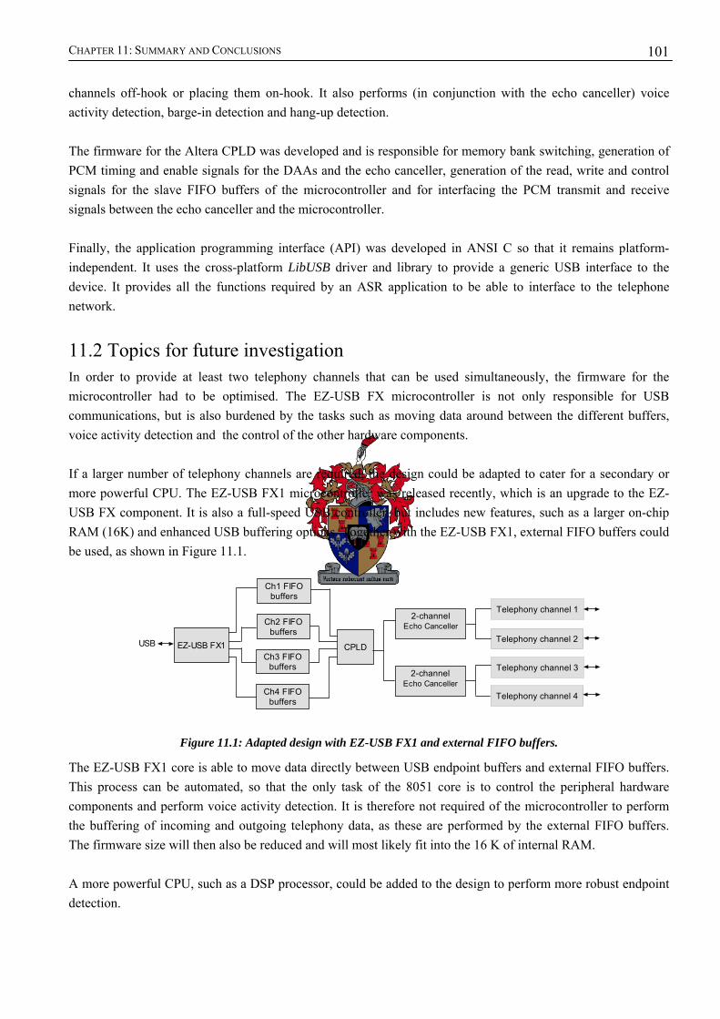
CHAPTER 11: SUMMARY AND CONCLUSIONS
101
channels off-hook or placing them on-hook. It also performs (in conjunction with the echo canceller) voice activity detection, barge-in detection and hang-up detection. The firmware for the Altera CPLD was developed and is responsible for memory bank switching, generation of PCM timing and enable signals for the DAAs and the echo canceller, generation of the read, write and control signals for the slave FIFO buffers of the microcontroller and for interfacing the PCM transmit and receive signals between the echo canceller and the microcontroller. Finally, the application programming interface (API) was developed in ANSI C so that it remains platform-independent. It uses the cross-platform LibUSB driver and library to provide a generic USB interface to the device. It provides all the functions required by an ASR application to be able to interface to the telephone network.
11.2 Topics for future investigation In order to provide at least two telephony channels that can be used simultaneously, the firmware for the microcontroller had to be optimised. The EZ-USB FX microcontroller is not only responsible for USB communications, but is also burdened by the tasks such as moving data around between the different buffers, voice activity detection and the control of the other hardware components. If a larger number of telephony channels are required, the design could be adapted to cater for a secondary or more powerful CPU. The EZ-USB FX1 microcontroller was released recently, which is an upgrade to the EZ-USB FX component. It is also a full-speed USB controller, but includes new features, such as a larger on-chip RAM (16K) and enhanced USB buffering options. Together with the EZ-USB FX1, external FIFO buffers could be used, as shown in Figure 11.1.
Figure 11.1: Adapted design with EZ-USB FX1 and external FIFO buffers.
The EZ-USB FX1 core is able to move data directly between USB endpoint buffers and external FIFO buffers. This process can be automated, so that the only task of the 8051 core is to control the peripheral hardware components and perform voice activity detection. It is therefore not required of the microcontroller to perform the buffering of incoming and outgoing telephony data, as these are performed by the external FIFO buffers. The firmware size will then also be reduced and will most likely fit into the 16 K of internal RAM. A more powerful CPU, such as a DSP processor, could be added to the design to perform more robust endpoint detection.
Telephony channel 1
Telephony channel 2
Telephony channel 3
Telephony channel 4
2-channelEcho Canceller
2-channelEcho Canceller
CPLDEZ-USB FX1
Ch1 FIFObuffers
Ch2 FIFObuffers
Ch3 FIFObuffers
Ch4 FIFObuffers
USB

CHAPTER 11: SUMMARY AND CONCLUSIONS
102
Another future possibility is to adapt the design to provide for ISDN channels, as single-chip ISDN interfaces are becoming available on the market. Companies such as Freescale, Infineon and Zarlink offer ISDN ICs or chipsets, which combine the line interface, PCM interface, controllers and codecs required to interface to an ISDN line.
11.3 Final conclusion The design goals of this project were to develop a low-cost, platform-independent telephony interface device that is easy to install and use and which provides adequate functionality to speech recognition applications. These goals have all been met. Although the EZ-USB FX microcontroller has limited processing capabilities, it successfully demonstrated the feasibility of designing a telephony interface device with a general-purpose CPU, low-cost components and non-proprietary software tools and libraries.
References
References [1] Compaq Computer Corporation, Hewlett-Packard Company, Intel Corporation, Lucent Technologies Inc,
Microsoft Corporation, NEC Corporation, Koninklijke Philips Electronics N.V, Universal Serial Bus Specification, Revision 2.0, April 27, 2000.
[2] John Hyde, USB design by Example, A Practical Guide to Building I/O Devices, Second Edition, Intel
Press, 2001. [3] Jan Axelson, USB Complete, Second Edition, Lakeview Research, 2001. [4] Cypress Semiconductor Corporation, CY7C6401/603/613 EZ-USB FX USB Microcontroller Data Sheet,
2000. [5] Sandeep Dutta, SDCC Compiler User Guide, SDCC 2.4.0, February 24, 2004.
http://sdcc.sourceforge.net/. [6] Don Anderson, Universal Serial Bus System Architecture, Mindshare Inc., May 2000. [7] The Linux USB project, http://www.linux-usb.org. [8] Brad Hards, The Linux USB sub-system, Sigma Bravo Pty Ltd, http://www.linux-usb.org/USB-
guide/book1.html. [9] Detlef Fliegl, Programming Guide for Linux USB Device Drivers, 2000, http://usb.cs.tum.edu. [10] Johannes Erdfelt, LibUSB Developers Guide, http://libusb.sourceforge.net. [11] Brooktrout Technology, Introduction to Computer Telephony, March 2002. [12] Silicon Laboratories, Si3050 Global Voice/Data Direct Access Arrangement, Rev 1.0, 2003. [13] Tim Danford, Basic Telephony Networking Circuits and Packet Telephony, Cisco Systems Inc. [14] Tomi Engdahl, Telephone line audio interface circuits, ePanaroma.net
(http://www.epanorama.net/links/telephone.html). [15] Cypress Semiconductor Corporation, EZ-USB FX, Getting Started Developer’s Kit, 2000. [16] Altera, Max 7000 Programmable Logic Device Family, July 1999, ver. 6.01.
REFERENCES
104
[17] Altera, Operating requirements for Altera devices, August 1999, ver. 9.01. [18] Power Innovations Limited, UK, TISP4125F3, TISP4150F3, TISP4180F3 Symmetrical Transient Voltage
Suppressors, March 1994, Revised September 1997. [19] Silicon Laboratories, AN67 Si3050/52/54/56 Layout Guidelines, Rev. 0.3 3/03, 2004. [20] Cypress Semiconductor Corporation, Design Considerations for In-System Reprogrammable (ISR)
Programming of Cypress CPLDs, November 9, 2001. [21] Brooktrout Technology, Echo Cancellation for ASR Applications, Keith Byerly, April 2002. [22] Silicon Laboratories, AN84 Digital Hybrid with the Si305x DAAs, Rev. 0.3 3/03. [23] Gordon J. Reesor, Echo in the PSTN – What is the worst case?, Zarlink Semiconductor, July 2003. [24] Texas Instruments, Digital Voice Echo Canceller with a TMS32020, application report: SPRA129,
Digital Signal Processing Solutions 1989. [25] Zarlink Semiconductor, CMOS MT9123 Dual Voice Echo Canceller Data Sheet, Issue 1, October 1996. [26] Freescale Semiconductor, Inc., Motorola Packet Telephony Echo Cancellation Solutions, White Paper
Series, July 2003. [27] Silicon Laboratories, AN128, Software SPI examples for the C8051F30X Family, Rev. 1.1. [28] Philips Semiconductor, 74LVC4245A Octal dual supply translating transceiver; 3-state, 30 March 2004. [29] Altera, AN75: High-speed board designs, November 2001, ver.4.0. [30] Howard W. Johnson, Martin Graham, High-Speed Digital Design: a handbook of black magic, 2002,
Prentice-Hall [31] Peter Alfke, Printed Circuit Board Design Considerations, Xilinx [32] Agilent Technologies, Surface Mount Chip LEDs, Technical Data. [33] Fairchild Semiconductor, 74LCX14 Low Voltage Hex Inverter with 5V Tolerant Schmitt Trigger Inputs,
March 1995, Revised February 2005. [34] Texas Instruments, USB Port Transient Suppressors, SN65220/65240/75240, July 2004. [35] Maxim, 5V/3.3V or Adjustable, Low-Dropout, Low IQ, 500mA Linear Regulators. MAX603/MAX604,
September 1994.
REFERENCES
105
[36] Horizon Electronics, Oscillators unit, Surface Mount Clock Oscillators HEOC31 – SMD 75 Ceramic lid. [37] Microchip Technology Inc., 24AA64/24LC64 64K I2C serial EEPROM. [38] Cypress Semiconductor, EZ-USB FX Technical Reference Manual, version 1.3, 2000. [39] Mark Zwoliński, Digital System Design with VHDL, Prentice Hall, 2000. [40] Cypress Semiconductor Corporation, CY7C1049BV 33, 512K x 8 Static RAM, September 13, 2002. [41] Lori F. Lamel, Lawrence R. Rabiner, Aaron E. Rosenberg, Jay G. Wilpon, An Improved Endpoint
Detector for Isolated Word Recognition, IEEE Transactions on Acoustics, Speech, and Signal Processing, Vol. ASSP-29, No. 4, August 1981.

Appendix A
Appendix A: Schematic design
Schematic design The next page presents the complete schematic design for the final prototype USB telephony interface device.
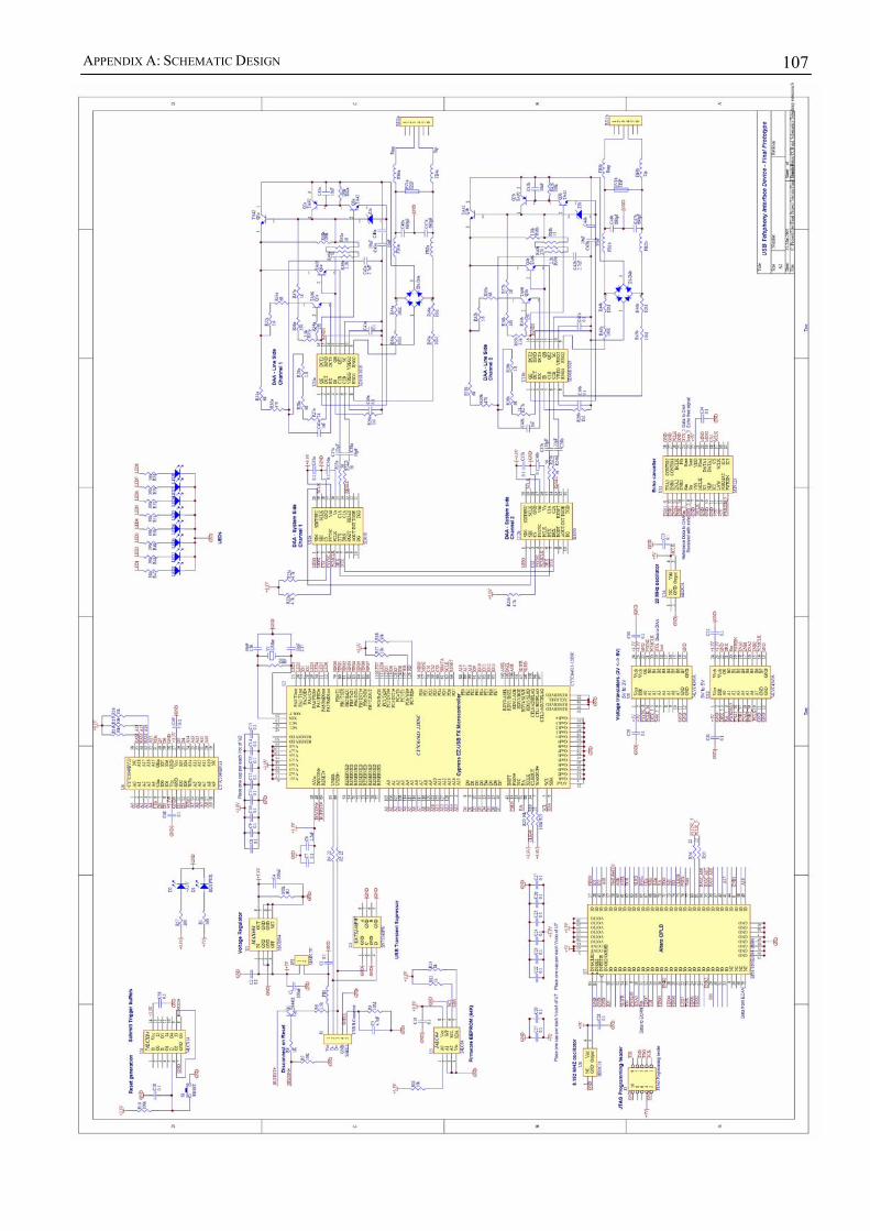
APPENDIX A: SCHEMATIC DESIGN
107
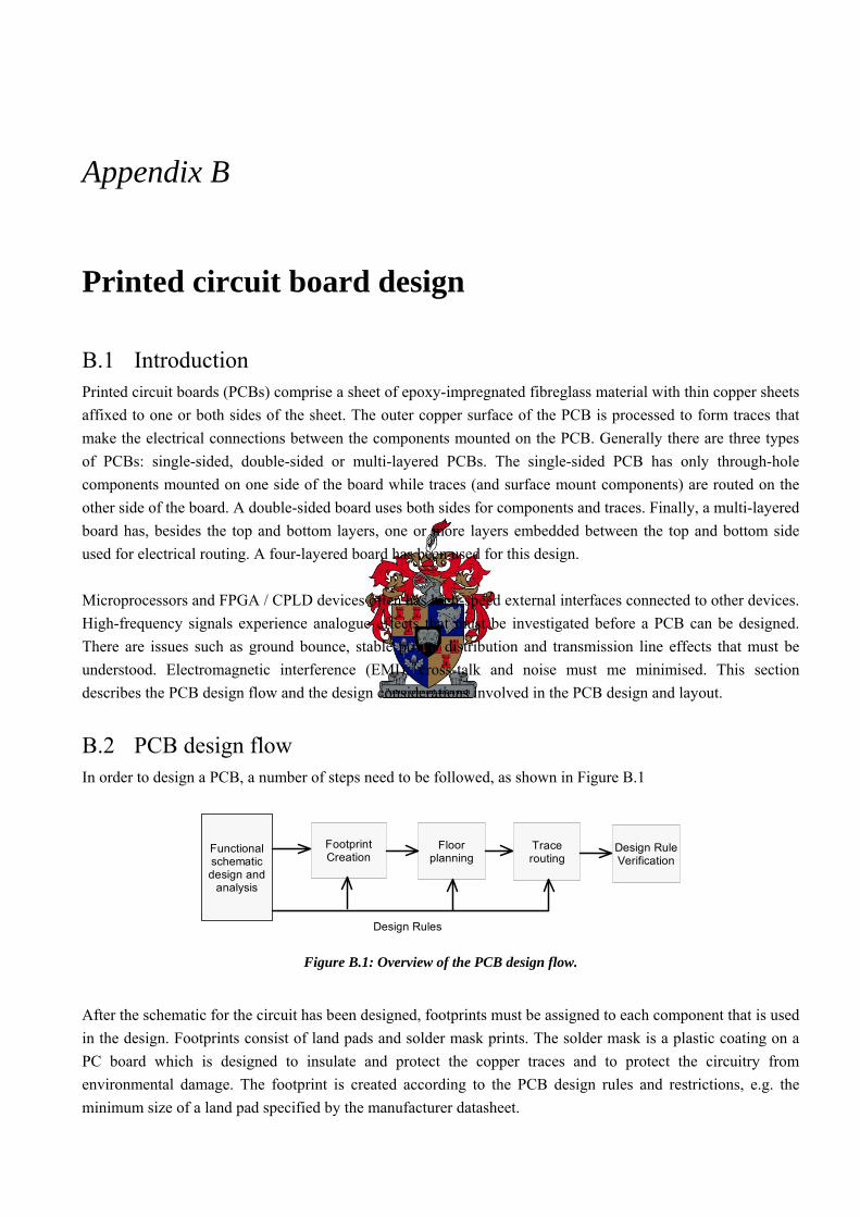
Appendix B
Appendix B: Printed circuit board design
Printed circuit board design
B.1 Introduction Printed circuit boards (PCBs) comprise a sheet of epoxy-impregnated fibreglass material with thin copper sheets affixed to one or both sides of the sheet. The outer copper surface of the PCB is processed to form traces that make the electrical connections between the components mounted on the PCB. Generally there are three types of PCBs: single-sided, double-sided or multi-layered PCBs. The single-sided PCB has only through-hole components mounted on one side of the board while traces (and surface mount components) are routed on the other side of the board. A double-sided board uses both sides for components and traces. Finally, a multi-layered board has, besides the top and bottom layers, one or more layers embedded between the top and bottom side used for electrical routing. A four-layered board has been used for this design. Microprocessors and FPGA / CPLD devices often has high-speed external interfaces connected to other devices. High-frequency signals experience analogue effects that must be investigated before a PCB can be designed. There are issues such as ground bounce, stable power distribution and transmission line effects that must be understood. Electromagnetic interference (EMI), cross-talk and noise must me minimised. This section describes the PCB design flow and the design considerations involved in the PCB design and layout.
B.2 PCB design flow In order to design a PCB, a number of steps need to be followed, as shown in Figure B.1
Functionalschematicdesign and
analysis
FootprintCreation
Floorplanning
Tracerouting
Design Rules
Design RuleVerification
Figure B.1: Overview of the PCB design flow.
After the schematic for the circuit has been designed, footprints must be assigned to each component that is used in the design. Footprints consist of land pads and solder mask prints. The solder mask is a plastic coating on a PC board which is designed to insulate and protect the copper traces and to protect the circuitry from environmental damage. The footprint is created according to the PCB design rules and restrictions, e.g. the minimum size of a land pad specified by the manufacturer datasheet.
APPENDIX B: PCB DESIGN
109
The floor planning is a layout of the components on the PCB so that they comply with the PCB design rules. PCB design rules that apply are, for example, the spacing between the DAA’s components, spacing from the digital ground plane etc. [19]. During floor planning, the layout for power distribution, user I/O (switches, buttons etc.) and external connectors must also be considered. Trace routing is the layout of traces on the PCB to create the electrical connections between the components. The usual order for routing signals is to start with critical traces such as high-frequency and high-voltage signals, because these signals usually have more routing constraints than the other signals. Design rules that apply during trace routing, are for example the minimum width constraint that must be adhered to for certain traces connected to the DAAs [19]. To ensure that all signals are routed correctly and that all the specified design rules are adhered to, design rule verification is performed to detect any errors. The Protel 99 SE software package has been used for the schematic design, footprint design, PCB layout and to perform design rule verification.
B.3 High-speed board designs When designing a PCB that contains high frequency signals (>25Mhz), it is important to consider the analogue effects of these signals, reduce noise in signals, minimise cross-talk between parallel traces and reduce the effect of ground-bounce.
B.3.1 Power filtering and distribution To filter low-frequency noise caused by power supplies, an electrolytic capacitor must be placed after the voltage regulator that provides the power supply to the PCB devices. Altera recommends using a 100μF electrolytic capacitor. Capacitors not only filter low-frequency noise from the power supply, but they also provide extra current when needed, such as when many outputs switch simultaneously in a circuit. A ferrite bead is also placed in series with the power supply. Ferrite beads have a minimal DC impedance, but at a higher frequency it generates an impedance which mainly consists of a resistive element. A ferrite bead is thus an effective component in noise suppression. PCB components add high-frequency noise to the PCB power planes. To filter this noise at a device, decoupling capacitors must be placed as close as possible to each of the power supply pins of the device. Placing the power and ground planes in parallel and on opposite sides of the PCB also reduces high-frequency noise, as the dielectric material of the PCB provides further bypass capacitance. If power planes are not used, the power traces on the PCB must be as wide as possible to reduce the DC resistance. The analogue and digital power planes must be separated to prevent unwanted interference between the two circuit types. There must be a dielectric width of at least 1 – 2.5 mm between the two power planes.
B.3.2 Clock signal routing The following principles must be applied during routing of clock signals to maximise the quality of the clock signal [29]:
• Clock traces should be as straight as possible.
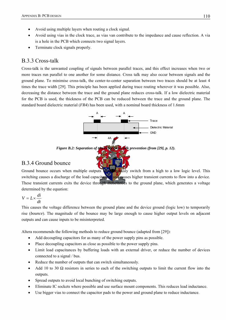
APPENDIX B: PCB DESIGN
110
• Avoid using multiple layers when routing a clock signal. • Avoid using vias in the clock trace, as vias van contribute to the impedance and cause reflection. A via
is a hole in the PCB which connects two signal layers. • Terminate clock signals properly.
B.3.3 Cross-talk Cross-talk is the unwanted coupling of signals between parallel traces, and this effect increases when two or more traces run parallel to one another for some distance. Cross talk may also occur between signals and the ground plane. To minimise cross-talk, the center-to-center separation between two traces should be at least 4 times the trace width [29]. This principle has been applied during trace routing wherever it was possible. Also, decreasing the distance between the trace and the ground plane reduces cross-talk. If a low dielectric material for the PCB is used, the thickness of the PCB can be reduced between the trace and the ground plane. The standard board dielectric material (FR4) has been used, with a nominal board thickness of 1.6mm
A A
4A
Trace
Dielectric Material
GND
Figure B.2: Separation of traces for cross-talk prevention (from [29], p. 12).
B.3.4 Ground bounce Ground bounce occurs when multiple outputs simultaneously switch from a high to a low logic level. This switching causes a discharge of the load capacitances and causes higher transient currents to flow into a device. These transient currents exits the device through inductances to the ground plane, which generates a voltage determined by the equation:
dtdiLV ×=
This causes the voltage difference between the ground plane and the device ground (logic low) to temporarily rise (bounce). The magnitude of the bounce may be large enough to cause higher output levels on adjacent outputs and can cause inputs to be misinterpreted. Altera recommends the following methods to reduce ground bounce (adapted from [29]):
• Add decoupling capacitors for as many of the power supply pins as possible. • Place decoupling capacitors as close as possible to the power supply pins. • Limit load capacitances by buffering loads with an external driver, or reduce the number of devices
connected to a signal / bus. • Reduce the number of outputs that can switch simultaneously. • Add 10 to 30 Ω resistors in series to each of the switching outputs to limit the current flow into the
outputs. • Spread outputs to avoid local bunching of switching outputs. • Eliminate IC sockets where possible and use surface mount components. This reduces lead inductance. • Use bigger vias to connect the capacitor pads to the power and ground plane to reduce inductance.
APPENDIX B: PCB DESIGN
111
• Connect each GND pin to the ground plane individually. These principles have been applied during the PCB design and layout.
B.3.5 Transmission lines When driving circuits, we need to consider whether a circuit interconnection must be treated as a simple interconnection (lumped circuit model) or as a transmission line. If the circuit is a transmission line, transmission line theory must be applied to determine the response of the circuit. A transmission line must be terminated properly, otherwise problems with ringing delays, overshoot and undershoot will occur [30]. We prefer to treat all traces, especially the ones that are being driven (clock signals) to be treated as a lumped circuit, as this will ease circuit design. We therefore need to determine the maximum trace lengths allowed for the traces to still be classified as a lumped circuit connection. The following equation determines the velocity ( pV ) at which signals will flow [29]:
(1)
where:
8103×=C
rE = relative dielectric constant of the PCB material. The propagation delay ( PDt ) for a given trace length ( l ) is given by:
P
PD Vlt = (2)
A circuit can be considered a lumped circuit if the signal edge rate ( PDt ) is greater than four times the propagation delay ( PDt ) [29]. The signal edge rate is the high-to-low or low-to-high transition time, and is a function of the load capacitance. In this design, the Altera CPLD generates the most of the clock signal outputs, and the CPLD’s output drive characteristics must therefore be investigated. The CPLD’s output signal has a falling edge that has a sharper edge rate than the rising edge, and is thus taken as the signal edge rate ( PDt ). The falling edge is more susceptible to transmission line effects. An equation based on the Altera CPLD’s output drive characteristics, is given for the falling edge rate ( Ft ) [29]:
PDt = CtF ×= 19.39 , (3)
where: C = load capacitance Substituting equation (1) and (3) into (2), and solving for l yields the following equation for the length at which the line must be treated as a transmission line:
R
F
ECtl
4×>
If this equation is solved for a typical load capacitance of 35pF, and if FR4 is used for the PCB material ( 1.4=RE ), the length at which the line must be treated as a transmission line is calculated to be 5.07 cm. The objective is thus to keep all traces, especially the clock signals, shorter than 5.07 cm. If the traces becomes longer, reflections could occur which would cause unwanted effects.
r
pECV =
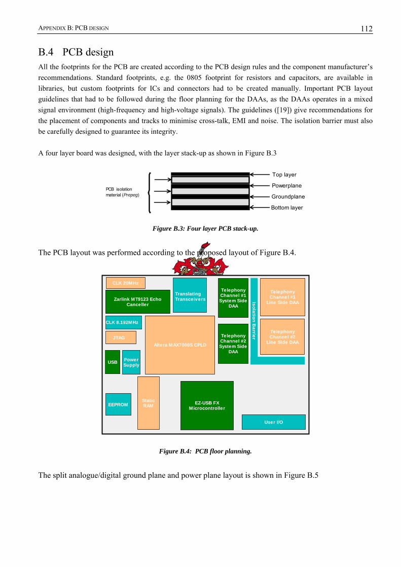
APPENDIX B: PCB DESIGN
112
B.4 PCB design All the footprints for the PCB are created according to the PCB design rules and the component manufacturer’s recommendations. Standard footprints, e.g. the 0805 footprint for resistors and capacitors, are available in libraries, but custom footprints for ICs and connectors had to be created manually. Important PCB layout guidelines that had to be followed during the floor planning for the DAAs, as the DAAs operates in a mixed signal environment (high-frequency and high-voltage signals). The guidelines ([19]) give recommendations for the placement of components and tracks to minimise cross-talk, EMI and noise. The isolation barrier must also be carefully designed to guarantee its integrity. A four layer board was designed, with the layer stack-up as shown in Figure B.3
Top layer
Powerplane
Groundplane
Bottom layer
PCB isolationmaterial (Prepeg)
Figure B.3: Four layer PCB stack-up.
The PCB layout was performed according to the proposed layout of Figure B.4.
TelephonyChannel #1System Side
DAAZarlink MT9123 Echo
Canceller
CLK 20MHz
Altera MAX7000S CPLD
TranslatingTransceivers
TelephonyChannel #1
Line Side DAA
TelephonyChannel #2System Side
DAA
TelephonyChannel #2
Line Side DAA
Isolation Barrier
EZ-USB FXMicrocontroller
User I/O
StaticRAM
USB
EEPROM
CLK 8.192MHz
JTAG
PowerSupply
Figure B.4: PCB floor planning.
The split analogue/digital ground plane and power plane layout is shown in Figure B.5

APPENDIX B: PCB DESIGN
113
Figure B.5: Power and ground plane layout.
The final floor plan layer (top) can bee seen in Figure B.6, and a photo of the populated PCB is shown in Figure B.7
Figure B.6: PCB top layer assembly drawings.
Digital Ground
AnalogueGround
3V
Ground plane Power plane
5V

APPENDIX B: PCB DESIGN
114
Figure B.7: Photo of assembled PCB.
B.5 Component and PCB cost
Table B.1: PCB and component cost estimation.
Table B.1 estimates the cost of the components and the PCB manufacturing cost. Please note that the PCM origination cost (R990) is a once-off cost for the first PCB. Duplicates of the PCB would cost R633.03
Description Estimated cost
EZ-USB FX microcontroller R88
Altera MAX7000S CPLD R240
Silicon Labs Si3050 DAA x 2 R66
Zarlink MT9123 echo canceller R40
512K Static RAM R29
64K I2C EEPROM R4.8
Voltage translators R25
USB transient suppressor R2.5
Hex Schmitt tigger, 74LCX14 R3
MAX604 voltage Regulator R18
Crystal – 12MHz R14.63
Oscillators 20Mhz & 8.192 MHz R80
passive components (resistors, capacitors), connectors and cables R291.21
PCB manufacturing R552
PCB testing R81.03
PCB origination R990
Total R2525.17

APPENDIX B: PCB DESIGN
115
(manufacturing and testing). Also, the price of some components is high, as they were not purchased in bulk quantities. If, for example, a batch of 10 boards were to be produced, the cost per board (including components) would be in the region of R1500 per board.
B.6 PCB bill of materials Table B.2 presents the PCB bill of materials, consisting of all the components used for the prototype design.
Manufacturer / Supplier Description Amount Molex 2m USB cable (Type A / Type B) 1
3M Rubber adhesive PCB mountings 4
Molex USB B-type connector (PCB, through-hole mount) 1
Molex 8x2 male header (JTAG connector) 1
Molex 1x2 male header (jumper) 1
Molex RJ11 socket 2
Molex PLCC 84 pin socket 1
Molex PDIP 28 pin socket 1
Conrad Miniature push button 1
Murata EMC suppression filter (ferrite), 100Ω @ 100 MHz – 1A 1
Multicomp 0.1uF capacitor, 0805, X7R, 10 % 36
Panasonic 100uF capacitor, electrolytic, 25V 2
Vishay/ Panasonic/ Phycomp 2.2uF capacitor, 1206, 16V 3
Vishay/ Panasonic/ Phycomp 4.7nF capacitor, 1206, 250V 1
Vishay/ Panasonic/ Phycomp 33pF capacitor, 0805, 20% 2
Murata 33pF capacitor, Y2, X7R 4
Murata 680pF capacitor, Y2, X7R 4
Vishay/ Panasonic/ Phycomp 1uF capacitor, tantalum, 10% 2
Vishay/ Panasonic/ Phycomp 2.7nF capacitor, 50V, X7R, 0805, 10% 2
Vishay/ Panasonic/ Phycomp 10nF capacitor, 250V, X7R 4
Vishay/ Panasonic/ Phycomp 10nF capacitor, 0805, 10% 2
Multicomp 560 Ω resistor, 0805, 1% 2
Multicomp 100kΩ resistor, 0805, 1% 7
Multicomp 22Ω resistor, 0805, 1% 3
Multicomp 1.5kΩ resistor, 0805, 1% 1
Multicomp 10kΩ resistor, 0805, 1% 4
Multicomp 1kΩ resistor, 0805, 1% 3
Multicomp 1 MΩ resistor,0805, 1% 3
Multicomp 4.7kΩ resistor, 0805, 1% 4
Multicomp 56Ω resistor, 0805, 1% 4
Multicomp 1kΩ resistor, 1206, 1% 2
Multicomp 68Ω resistor, 1206, 1% 4
Multicomp 470Ω resistor, 1206, 1% 2
Multicomp 2.2kΩ resistor, 1206, 1% 2
Multicomp 5.6Ω resistor, 1% 2
Multicomp 68 Ω resistor, 2512, 1W 2
Multicomp 150Ω resistor, 0805, 1% 2
Multicomp 3.3kΩ resistor, 1206, 1% 2
Multicomp 330Ω resistor, 1206, 1% 2
Multicomp 18Ω resistor, 1206, 1% 4
Multicomp 270Ω resistor, 1206, 1% 2
Multicomp 10MΩ resistor, 5% 4
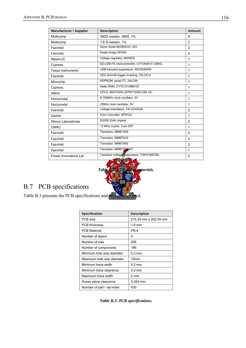
APPENDIX B: PCB DESIGN
116
Manufacturer / Supplier Description Amount Multicomp 390Ω resistor, 0805, 1% 8
Multicomp 1.8 Ω resistor, 1% 2
Fairchild Zener diode BZX85C43, 43V 2
Fairchild Diode bridge DF04S 2
Maxim-IC Voltage regulator, MAX604 1
Cypress EZ-USB FX microcontroller, CY7C64613-128NC 1
Texas Instruments USB transient suppressor, SN75240PW 1
Fairchild HEX Schmitt trigger inverting, 74LCX14 1
Microchip EEPROM, serial I2C, 24LC64 1
Cypress Static RAM, CY7C10149BV33 1
Altera CPLD, MAX7000s (EPM7160SLC84-10) 1
Horizonxtal 8.192MHz clock oscillator, 5V 1
Horizonxtal 20Mhz clock oscillator, 5V 1
Fairchild Voltage translators, 74LVC4245A 2
Zarlink Echo Canceller, MT9123 1
Silicon Laboratories Si3050 DAA chipset 2
CMAC 12 MHz crystal, 2-pin DIP 1
Fairchild Transistor, MMBTA06 4
Fairchild Transistor, MMBTA42 2
Fairchild Transistor, MMBTA92 2
Fairchild Transistor, MMBT2N4401 1
Power Innovations Ltd Transient Voltage Suppressor, TISP4180F3SL
2
Table B.2: PCB bill of materials.
B.7 PCB specifications Table B.3 presents the PCB specifications and design rules used.
Table B.3: PCB specifications.
Specification Description PCB size 215.34 mm x 202.04 mm
PCB thickness 1.6 mm
PCB Material FR-4
Number of layers 4
Number of vias 206
Number of components 186
Minimum hole size diameter 0.3 mm
Maximum hole size diameter 10mm
Minimum trace width 0.2 mm
Minimum trace clearance 0.2 mm
Maximum trace width 2 mm
Power plane clearance 0.254 mm
Number of pad / via holes 430
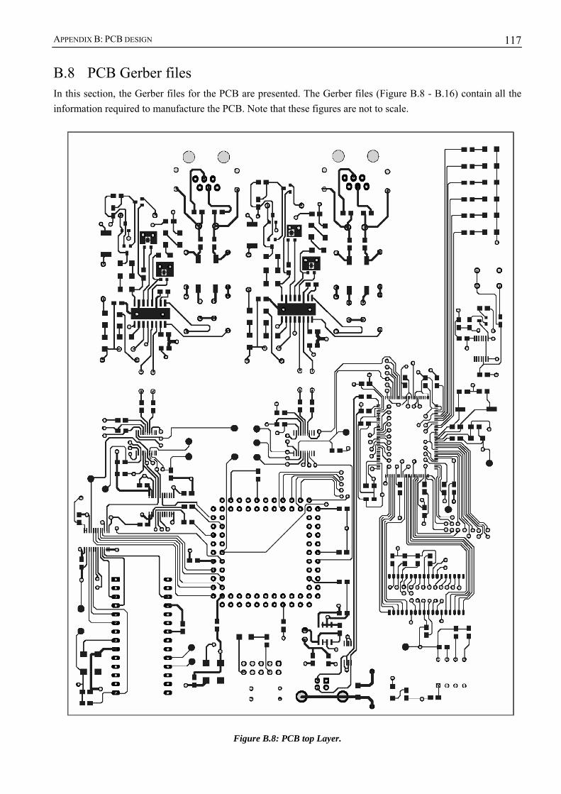
APPENDIX B: PCB DESIGN
117
B.8 PCB Gerber files In this section, the Gerber files for the PCB are presented. The Gerber files (Figure B.8 - B.16) contain all the information required to manufacture the PCB. Note that these figures are not to scale.
Figure B.8: PCB top Layer.
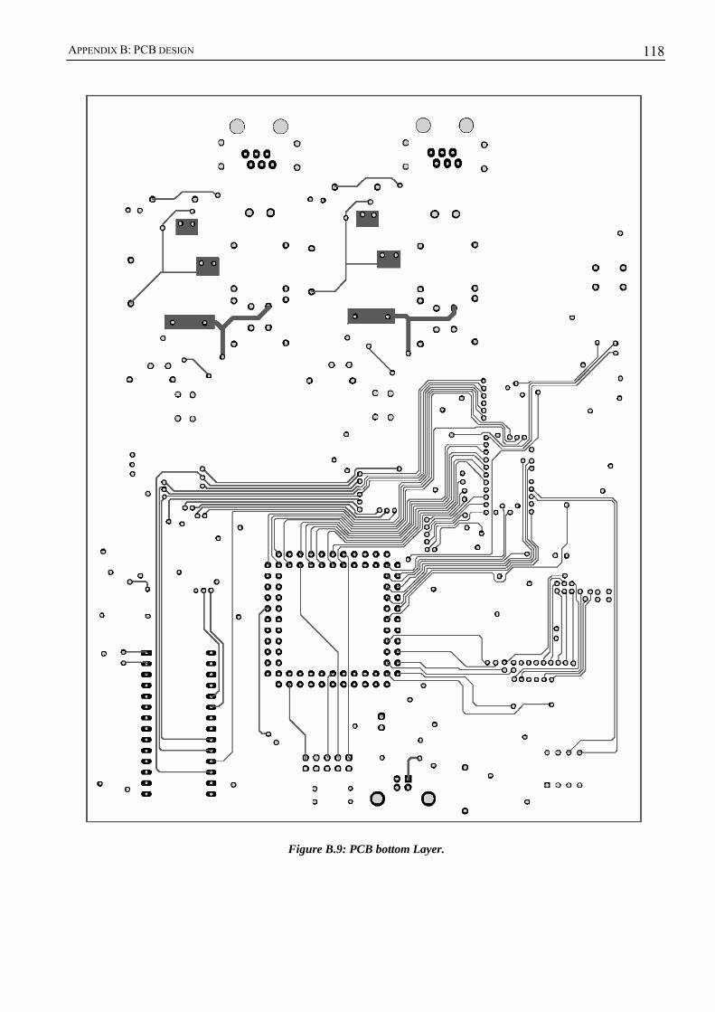
APPENDIX B: PCB DESIGN
118
Figure B.9: PCB bottom Layer.
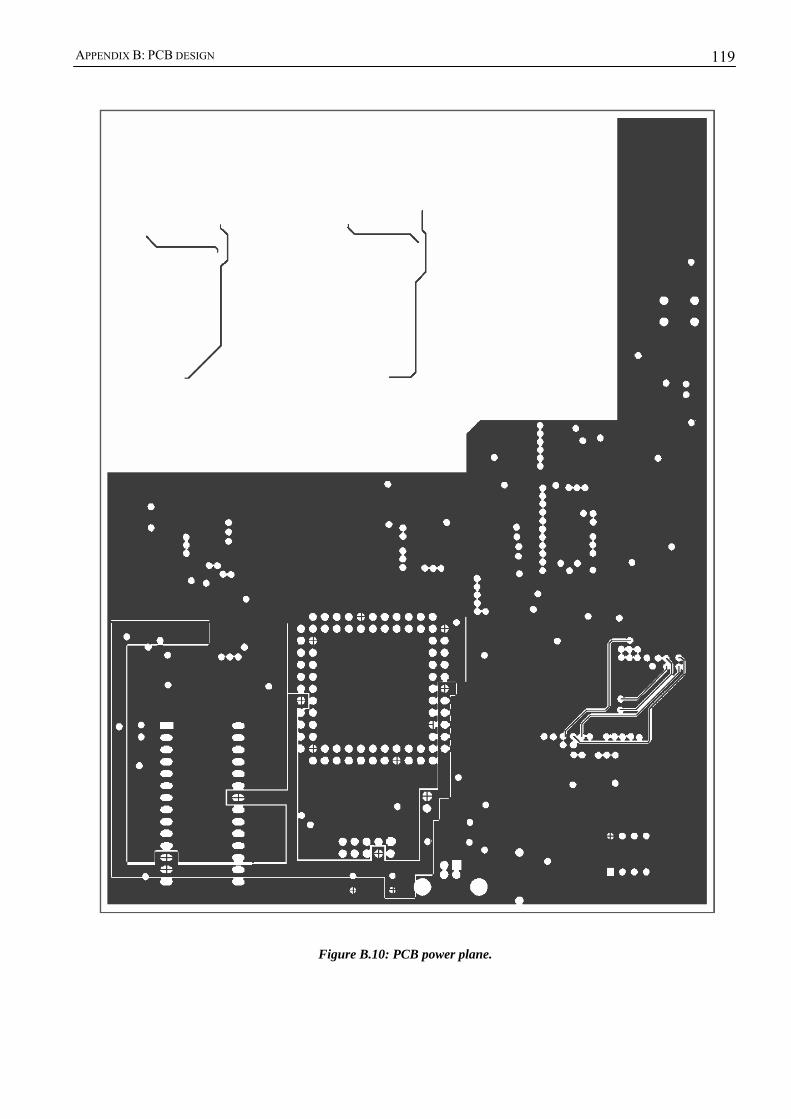
APPENDIX B: PCB DESIGN
119
Figure B.10: PCB power plane.
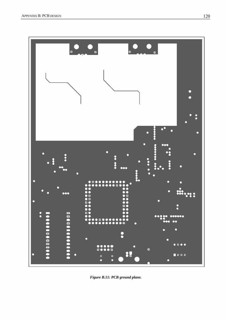
APPENDIX B: PCB DESIGN
120
Figure B.11: PCB ground plane.
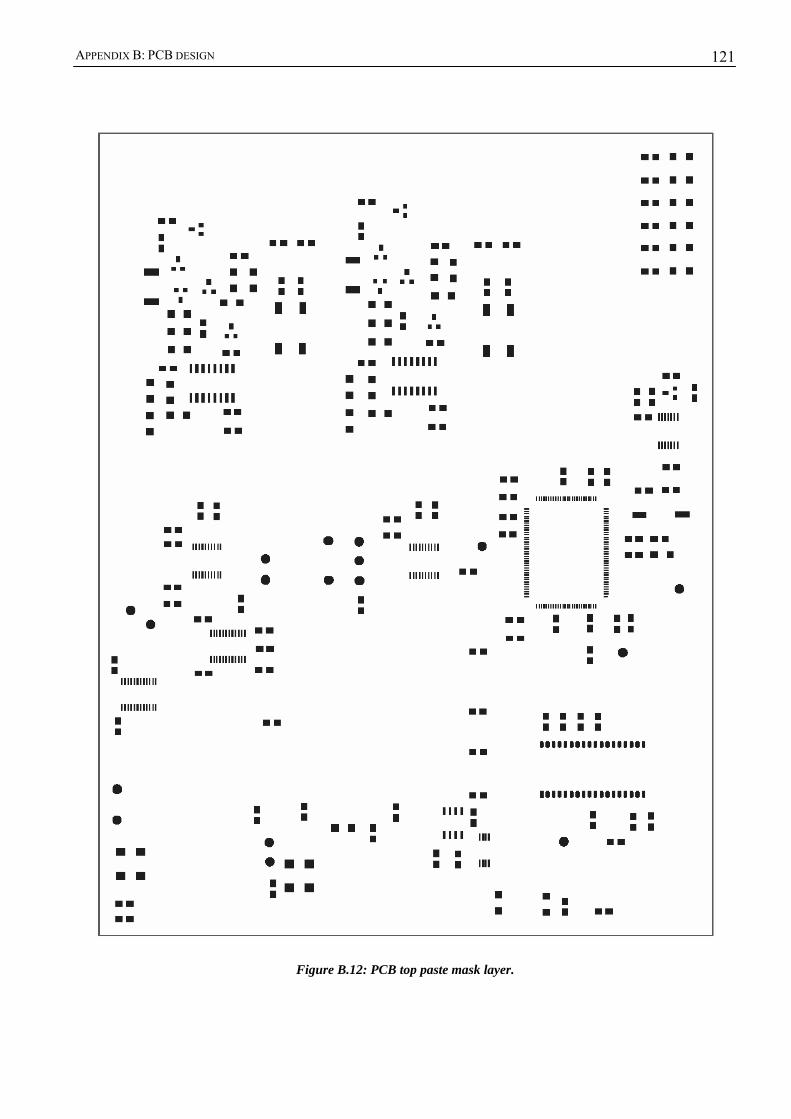
APPENDIX B: PCB DESIGN
121
Figure B.12: PCB top paste mask layer.
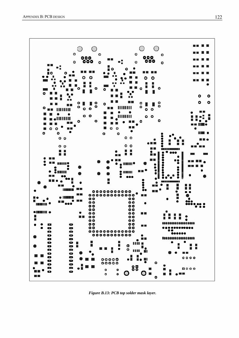
APPENDIX B: PCB DESIGN
122
Figure B.13: PCB top solder mask layer.
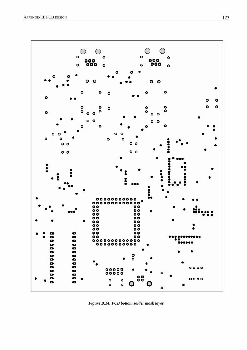
APPENDIX B: PCB DESIGN
123
Figure B.14: PCB bottom solder mask layer.
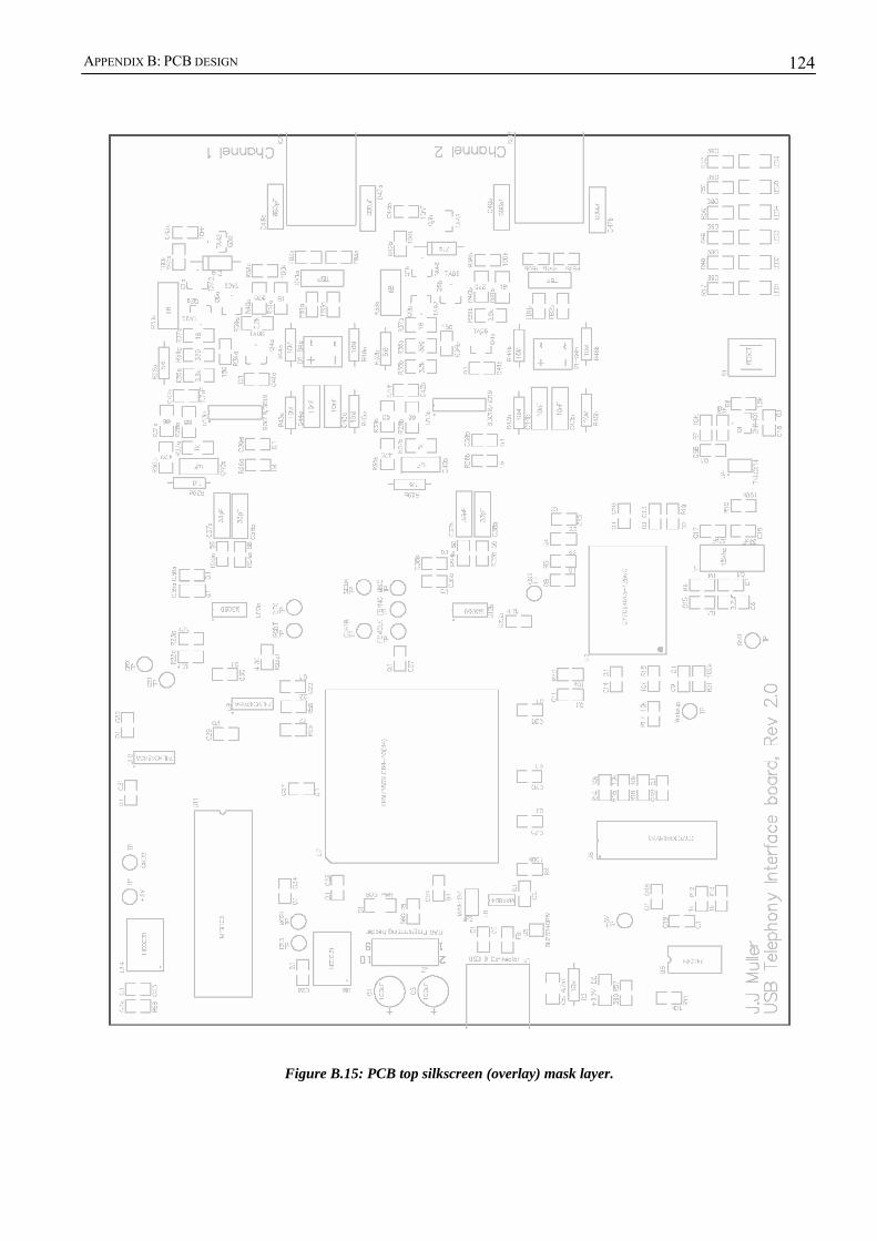
APPENDIX B: PCB DESIGN
124
Figure B.15: PCB top silkscreen (overlay) mask layer.
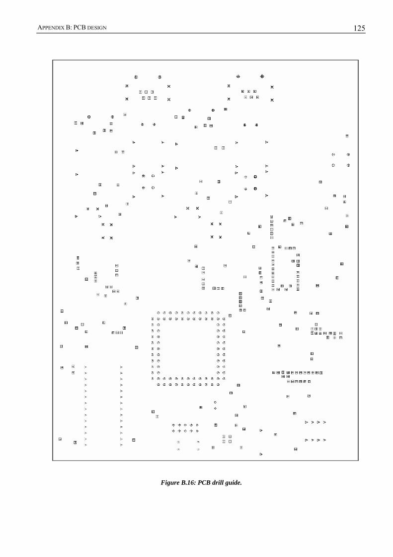
APPENDIX B: PCB DESIGN
125
Figure B.16: PCB drill guide.
Appendix C
Appendix C: Firmware functions
Firmware functions C.1 Boot loader firmware This section describes the functions of the boot loader firmware for the EZ-USB FX microcontroller. Please refer to the source code, which can be found on the CD-ROM in the ‘\firmware\Bootloader’ directory, for details regarding these functions.
RAM_bankselect Prototype: void RAM_bankselect(Byte Bank)
This function changes the memory bank to use for data access. Code is always stored and fetched from bank 0, regardless which data bank is selected. The three highest address lines (A16,A17, A18) of the 512 K RAM are used for selecting the memory bank.
Inputs: Bank – The memory bank (0-7) to use for next data read or write operation.
config_ports Prototype: void config_ports()
This function selects the function of the I/O ports and configures the pins as inputs or outputs.
Device_init Prototype: void Device_init()
This function turns on the LEDs, which indicate that the microcontroller is functioning and that the boot loader is ready to receive firmware data.
setup_int Prototype: void setup_int()
This function enables the USB and endpoint interrupts that are allowed. Only the interrupts for standard USB requests and endpoint 3 OUT transfers are enabled.
do_RAM_download Prototype: void do_RAM_download()
APPENDIX C: FIRMWARE FUNCTIONS
127
This function writes the data that is received from the host via a control transfer, to external RAM. The number of bytes to write and the memory address are specified in the setup data packet of the control transfer.
do_get_descriptor Prototype: void do_get_descriptor()
This function determines which descriptor is requested, and loads the Setup Data Pointer (SUDPTR) with the memory address of the requested descriptor. The Setup Data Pointer is used to read descriptor information and transfer it to the host.
do_std_dev_in Prototype: void do_std_dev_in()
This function handles standard device requests where device information must be transferred to the host PC. If a device descriptor was requested, the do_get_descriptor() function is called.
do_std_dev_out Prototype: void do_std_dev_out()
This function handles standard device requests where data was sent by the host PC. Typical requests are to set the device address, configuration or a feature.
do_std_if_in Prototype: void do_std_if_in()
This function handles standard interface requests where interface information must be transferred to the host PC. If an interface descriptor was requested, the do_get_descriptor() function is called.
do_std_if_out Prototype: void do_std_if_out()
This function handles standard interface requests where data was sent by the host PC. Typical requests are to set or clear interface settings and features.
do_std_ep_in Prototype: void do_std_ep_in()
This function handles standard endpoint requests where endpoint information must be transferred to the host PC.
do_std_ep_out Prototype: void do_std_ep_out()
APPENDIX C: FIRMWARE FUNCTIONS
128
This function handles standard endpoint requests where data was sent by the host PC. Typical requests are to set or clear endpoint features.
parser Prototype: void parser()
This function determines the type of standard request that was sent by the host PC, and calls one of the ‘do’-functions to respond to the request.
usb_isr() Prototype: void usb_isr()
The USB interrupt service routine, which is automatically called when interrupt 8 (USB interrupts) occur. It determines the type USB interrupt that occurred (Setup Data Available, endpoint etc.) and performs the actions required for the specific USB interrupt.
C.2 Telephony interface device firmware This section describes the functions of the telephony interface firmware for the EZ-USB FX microcontroller. The telephony interface firmware share the following basic functions with the boot loader firmware: RAM_BankSelect, config_ports, Device_init, setup_int, do_get_descriptor, do_std_dev_in, do_std_dev_out, do_std_if_in, do_std_if_out, do_std_ep_in, do_std_ep_out, parser, usb_isr. Please refer to the source code, which can be found on the CD-ROM in the ‘\firmware\Telephony_interface’ directory, for details regarding these functions.
C2.1 General functions apply_reset_values Prototype: void apply_reset_values()
This function apply the default values to all the buffer indices, VAD parameters and control flags and variables. This function is called when the device is initialised.
ChannelCommand Prototype: void ChannelCommand()
This function is called by the USB interrupt service routine if data is sent from the host PC to endpoint 3. Endpoint 3 is used by the API to send commands relating to the telephony interface. This function decodes the command byte that was sent to determine the appropriate action to take.
Fifo_ISR Prototype: void Fifo_ISR()
APPENDIX C: FIRMWARE FUNCTIONS
129
This function is automatically called when a FIFO interrupt occurs (interrupt service routine). FIFO interrupts are generated when a FIFO buffer overflow or underflow occurred. This function determines which FIFO generated the interrupt, and turns a LED on to indicate an error condition.
timer0_ISR Prototype: void timer0_ISR()
This is the interrupt service routine which is called when timer 0 overflows. The function only increments a counter variable, which is used to time certain events for channel 1 when it is activated.
timer1_ISR Prototype: void timer1_ISR()
This is the interrupt service routine which is called when timer 1 overflows. The function only increments a counter variable, which is used to time certain events for channel 2 when it is activated.
SendBufferedDataToTelephone Prototype: void SendBufferedDataToTelephone(FIFOBuffer *TheBuffer, int
nBytes, Byte channel)
This function is called when there is buffer space available in the outgoing slave FIFO buffer of a channel. It would use DMA transfers to transfer nBytes from RAM to the channel FIFO buffer. Data to be sent over the telephone line, is buffered in the RAM bank associated with the channel. The read and write indices for this buffer are stored in the FIFOBuffer structure. Data placed in the outgoing FIFO buffer will be read by the DAA and be sent over the telephone line.
Inputs: *TheBuffer – Pointer to a structure containing the buffer indices. nBytes - The number of bytes to transfer. channel – The channel where data must be transferred to.
GetDataFromTelephone Prototype: void GetDataFromTelephone(FIFOBuffer *TheBuffer, int nBytes, Byte
channel)
This function is called when there is data available to be read from the incoming slave FIFO buffer of a channel. It would use DMA transfers to transfer nBytes from the FIFO buffer to a RAM buffer. Data received from the telephone channel is buffered in RAM in the memory bank associated with the channel. The read and write indices for this buffer are stored in the FIFOBuffer structure. Data placed in the RAM buffer will later be sent to the host PC.
Inputs: *TheBuffer – Pointer to a structure containing the buffer indices. nBytes - The number of bytes to transfer. channel – The channel from where data must be read.
APPENDIX C: FIRMWARE FUNCTIONS
130
BufferDataFromPC Prototype: void BufferDataFromPC(FIFOBuffer *TheBuffer, Byte channel)
This function is called when there is an IN transfer (data sent from host PC) in progress. Data collected in the IN endpoint will be transferred to RAM using DMA transfers. The data is written to the memory bank associated with the channel. The read and write indices for this buffer are stored in the FIFOBuffer structure. This data will be read at a later stage, and sent to the telephone channel.
Inputs: *TheBuffer – Pointer to a structure containing the buffer indices. channel – The channel to where data must be transferred to.
SendBufferedDataToPC Prototype: void SendBufferedDataToPC(FIFOBuffer *TheBuffer, Byte channel)
This function is called when there is an OUT transfer (data sent to host PC) in progress. Data is fetched from the RAM buffer, using DMA transfers, and placed in an endpoint buffer from where it will be sent to the PC. Data is read from the memory bank associated with the channel. The read and write indices for this buffer are stored in the FIFOBuffer structure.
Inputs: *TheBuffer – Pointer to a structure containing the buffer indices. channel – The channel to fetch data from.
InitCallTransfer Prototype: void InitCallTransfer()
This function enables hang-up tone detection, initialises variables and sets the flags that would allow a call transfer to take place.
DoCallTransfer Prototype: void DoCallTransfer( int nBytes, FIFOBuffer *SrcBuffer, FIFOBuffer
*DstBuffer)
This function is called when there is a call transfer in progress. It will copy nBytes of data from the incoming buffer for a channel (buffer information contained in *SrcBuffer) to the outgoing buffer of the other channel (buffer information contained in *DstBuffer.
Inputs: nBytes – The number of bytes to transfer. *SrcBuffer – Structure containing source buffer indices. *DstBuffer – Structure containing destination buffer indices.
EndCallTransfer Prototype: void EndCallTransfer()
If a hang-up condition has been detected, this function will end the a call-transfer by placing both channels back on-hook.
APPENDIX C: FIRMWARE FUNCTIONS
131
C2.2 DAA functions These functions relate to the DAAs, and uses the SPI bus to read or write the DAA registers.
WriteByte Prototype: void WriteByte(Byte byte_to_write)
This function writes a single byte to the SPI bus by appropriately toggling (“bit banging”) the MOSI (Master Out Slave In) , CS (chip select) and the SCLK (serial clock) pins.
Inputs: byte_to_write – The byte that we wish to write on the SPI bus.
ReadByte Prototype: Byte ReadByte()
This function reads a single byte from the SPI bus by appropriately toggling (“bit banging”) the CS (chip select) and the SCLK (serial clock) pins and reading the MISO (Master In Slave Out) pins.
Outputs: Byte – The byte that was read from the SPI bus.
SPI_write_reg Prototype: void SPI_write_reg(Byte channel, int address, Byte value)
This function writes three bytes to the SPI bytes by using the WriteByte() function. The three bytes are the control byte, address byte and the value byte. The control byte determines the DAA channel to which the value must be written. The second byte contains the address of the register that we wish to write, and the third byte contains the value to be written.
Inputs: channel – The channel number that the write operation applies to. address - The register address that we wish to write. value – The value that is written to the register.
SPI_read_reg Prototype: void SPI_read_reg(Byte channel, int address)
This function writes two bytes to the SPI bytes by using the WriteByte() function. The two bytes are the control byte and the address byte. The control byte determines the DAA channel from which a register value must be read. The second byte contains the address of the register that we wish to read. The value of this register is then returned on the SPI bus, and is read by using the ReadByte() function.
Inputs: channel – The channel number that the read operation applies to. address - The register address that we wish to read.
DAA_init Prototype: void DAA_init()
This function initialises the DAAs by resetting the devices. After the devices have been reset, they are configured by setting the required parameters such as the AC and DC termination, the timeslot allocations for
APPENDIX C: FIRMWARE FUNCTIONS
132
PCM transfers, the SPI/PCM communications mode, the companding method used (A-law) and the ring validation parameters.
DAA_off_hook Prototype: Byte DAA_off_hook(Byte channel)
This function takes the specified channel off-hook.
Inputs: channel – The channel to take off-hook. Outputs: Byte – Indicates success or failure.
0 = Channel successfully taken off-hook. 1 = Failure (insufficient line current).
DAA_on_hook Prototype: Byte DAA_on_hook(Byte channel)
This function places the specified channel on-hook.
Inputs: channel – The channel to place on-hook. Outputs: Byte – Indicates success or failure.
0 = Channel successfully taken off-hook. 1 = Failure.
DAA_check_ringing Prototype: Byte DAA_check_ringing(Byte channel)
This function checks if the ring detect flag for a channel is set. If it set, the timer is reset and activated. If the timer expired before a second ringing signal was received, the channel status will be set to ON_HOOK.
Inputs: channel – The channel to query. Outputs: Byte – Indicates status of the channel (ON_HOOK or RINGING).
DAA_status Prototype: Byte DAA_status(Byte channel)
If the channel is on-hook, this function will call the DAA_check_ringing() function to check for a ringing signal. It also measures the line voltage to check if a line is connected.
Inputs: channel – The channel to query. Outputs: Byte – Indicates status of the channel (ON_HOOK, OFF_HOOK, RINGING or NO_LINE).
Test_DAA Prototype: Byte Test_DAA(Byte channel)
This function reads a arbitrary register from of the DAA and writes the value that was read back to the register. This is only to test to SPI communications interface between the microcontroller and the DAA.
Inputs: channel – The channel to test.

APPENDIX C: FIRMWARE FUNCTIONS
133
Outputs: Byte – Indicates success or failure. 0 = Success, SPI communications successful 1 = Failure, could not communicate with DAA.
C2.3 Echo canceller functions The following functions relate to the echo canceller.
EC_write_register Prototype: void EC_write_register(Byte address, Byte io_byte)
This function toggles (“bit banging”) the echo canceller CS3 (chip select), MOSI (Master Out Slave In) and SCLK (serial clock) pins connected to the microcontroller to write two bytes to the SPI bus. The first byte is the address of the register that must be written, and the second byte is the value that must be written to the register.
Inputs: address – The address of the echo canceller’s register that must be accessed. io_byte – The byte to be written to the register.
EC_read_register Prototype: Byte EC_read_register(Byte address)
This function toggles the echo canceller CS3 (chip select) and SCLK (serial clock) pins connected to the microcontroller to write one byte on the SPI bus (the address of a register). A byte is then returned on the SPI bus, which is the value of the requested register.
Inputs: address – The address of the echo canceller’s register that must be accessed. Outputs: Byte – The value of the register.
EC_init Prototype: void EC_init()
This function initialises both channels of the echo canceller by resetting the device.
TestEC Prototype: Byte TestEC()
This function reads a arbitrary register from of the echo canceller and writes the value that was read back to the register. This is only to test to SPI communications interface between the microcontroller and the echo canceller.
Outputs: Byte – Indicates success or failure 0 = Success, SPI communications successful 1 = Failure, could not communicate with the echo canceller.
APPENDIX C: FIRMWARE FUNCTIONS
134
C2.4 Voice activity detection The functions in this section relate to voice activity, barge-in and hang-up tone detection.
DoubleTalkDetect Prototype: BOOLEAN DoubleTalkDetect(Byte Channel)
This function reads the double-talk detection flag of the echo canceller to determine if the echo canceller detected a double-talk condition. This is used to trigger the voice activity detection algorithm. It also performs other housekeeping, such as checking if timers have expired since the last time that voice activity was detected. Finally, a flag is set if a long silence is detected in the incoming signals (used to detect a hang-up condition during a call transfer).
Inputs: channel – The channel to query. Outputs: BOOLEAN – Indicates whether or not a double-talk condition was detected.
0 (FALSE) = No double-talk detected. 1 (TRUE) = Double-talk detected.
VoiceActivityDetection Prototype: void VoiceActivityDetection(Byte Channel)
This function performs voice activity detection. If a double-talk condition was detected, the VAD algorithm is activated so that the energy and ZCR per frame can be measured in the GetDataFromTelephone()function. These measurements are performed on new incoming telephony data. If the measurements span one frame, this function will check if the measured energy and ZCR are above threshold values. If the measurements are above the threshold values for a number of frames, voice activity is indicated (as well as barge-in if barge-in detection was enabled). Also, if the device is configured to record data upon voice activity, the function will allow new data to be buffered until the end of the utterance is detected (no voice activity detected for a period). If the energy and ZCR measurements indicate that no voice activity is present, the VAD algorithm will be disabled until the echo canceller again detects a double-talk condition.
Inputs: channel – The channel on which voice activity detection is performed.
HangupDetection Prototype: void HangupDetection(Byte Channel)
This function is similar to the VoiceActivityDetection(). It is called when a call transfer is active, and uses the energy and ZCR measurements to detect a hang-up tone. For a hang-up tone to be detected, the measured energy and ZCR must fall within a certain range for a defined time interval.
Inputs: channel – The channel on which hang-up tone detection is performed.
ClearBuffer Prototype: void ClearBuffer(Byte Channel)
This function is called when barge-in detection is enabled and a barge-in condition was detected. It erases the remaining buffered data to stop the prompt currently being played to the caller.
Inputs: channel – The channel of which the buffers must be erased.
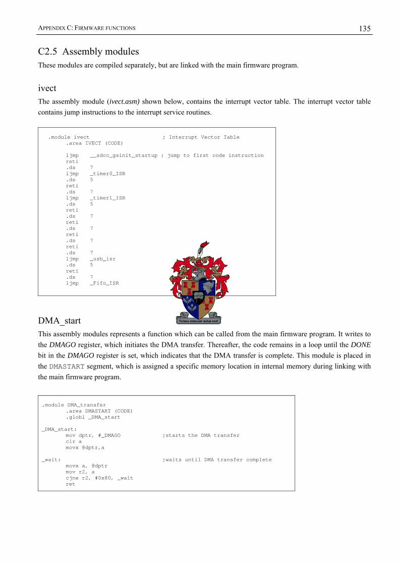
APPENDIX C: FIRMWARE FUNCTIONS
135
C2.5 Assembly modules These modules are compiled separately, but are linked with the main firmware program.
ivect The assembly module (ivect.asm) shown below, contains the interrupt vector table. The interrupt vector table contains jump instructions to the interrupt service routines.
.module ivect ; Interrupt Vector Table .area IVECT (CODE) ljmp __sdcc_gsinit_startup ; jump to first code instruction reti .ds 7 ljmp _timer0_ISR .ds 5 reti .ds 7 ljmp _timer1_ISR .ds 5 reti .ds 7 reti .ds 7 reti .ds 7 reti .ds 7 ljmp _usb_isr .ds 5 reti .ds 7 ljmp _Fifo_ISR
DMA_start This assembly modules represents a function which can be called from the main firmware program. It writes to the DMAGO register, which initiates the DMA transfer. Thereafter, the code remains in a loop until the DONE bit in the DMAGO register is set, which indicates that the DMA transfer is complete. This module is placed in the DMASTART segment, which is assigned a specific memory location in internal memory during linking with the main firmware program. .module DMA_transfer .area DMASTART (CODE) .globl _DMA_start _DMA_start: mov dptr, #_DMAGO ;starts the DMA transfer clr a movx @dptr,a _wait: ;waits until DMA transfer complete movx a, @dptr mov r2, a cjne r2, #0x80, _wait ret
Appendix D Appendix D: Miscellaneous API functions Miscellaneous API functions This section contains functions that are included in the API, but which does not directly relate to the operations of the telephony interface device.
D.1 File I/O The section describes API functions that transfers audio data between files and the telephony buffers.
LoadTelephonyBufferFromAlawFile Prototype: void LoadTelephonyBufferFromAlawFile(char *Filename,
TelephonyBuffer *TheBuffer)
This function opens a file that contains A-law samples, and reads them into the outgoing buffer of the specified channel.
Inputs: *Filename – The name of the file to open. *TheBuffer – The buffer to which the audio samples must be copied to.
Outputs: None. SaveTelephonyBufferAsWaveFile
Prototype: void SaveTelephonyBufferAsWaveFile(TelephonyBuffer *TheBuffer)
This function converts the A-law samples contained in the specified incoming telephony buffer to linear values, and saves the data to a file in the WAVE file format. The filename used by this function is set by the SetTelephonyBufferRecordFile() function.
Inputs: *TheBuffer – The buffer from which to copy the audio samples. Outputs: None.
SaveTelephonyBufferAsAlawFile
Prototype: void SaveTelephonyBufferAsAlawFile(TelephonyBuffer *TheBuffer)
This function copies A-law samples directly from the specified incoming telephony buffer to a file. The filename used by this function is set by the SetTelephonyBufferRecordFile() function.
Inputs: *TheBuffer – The buffer from which to copy the audio samples. Outputs: None.

APPENDIX D: MISCELLANEOUS API FUNCTIONS
137
SetTelephonyBufferRecordFile
Prototype: int SetTelephonyBuffer RecordFile(char * filename, TelephonyBuffer
*TheBuffer)
Sets the record file name for a telephone channel.
Inputs: *filename – Name of the file to use for recording. TheBuffer – The buffer for which to set the record file name.
Outputs: None.
Related Documents