July 2008 Rev 1 1/66 UM0527 User manual UPS evaluation board Introduction The UPS evaluation board provides a complete solution addressing the low/medium range UPS segment with 700 V A output power capab ility . The evaluation board, from a hardware and firmware point of view , is ready to support the development of a complete solution. Thanks to the PC software it's possible to monitor all the relevant system parameters using the RS232 interface or the USB. The evaluation board is available for the 120 Vac market and 230 Vac market. The UPS evaluation board is built in offline topology with AVR regulation of the mains boost and buck. The inverter module contains the push-pull DC/DC converter and the DC/AC output full-bridge generating quasi-sine waveform. www.st.com

Welcome message from author
This document is posted to help you gain knowledge. Please leave a comment to let me know what you think about it! Share it to your friends and learn new things together.
Transcript
7/22/2019 UPSSG3525
http://slidepdf.com/reader/full/upssg3525 1/66
July 2008 Rev 1 1/66
UM0527User manual
UPS evaluation board
Introduction
The UPS evaluation board provides a complete solution addressing the low/medium rangeUPS segment with 700 VA output power capability. The evaluation board, from a hardwareand firmware point of view, is ready to support the development of a complete solution.Thanks to the PC software it's possible to monitor all the relevant system parameters usingthe RS232 interface or the USB. The evaluation board is available for the 120 Vac marketand 230 Vac market.
The UPS evaluation board is built in offline topology with AVR regulation of the mains boostand buck. The inverter module contains the push-pull DC/DC converter and the DC/ACoutput full-bridge generating quasi-sine waveform.
www.st.com

7/22/2019 UPSSG3525
http://slidepdf.com/reader/full/upssg3525 2/66
Contents UM0527
2/66
Contents
1 General description . . . . . . . . . . . . . . . . . . . . . . . . . . . . . . . . . . . . . . . . . . 5
1.1 Hardware architecture . . . . . . . . . . . . . . . . . . . . . . . . . . . . . . . . . . . . . . . . 5
1.1.1 General realization . . . . . . . . . . . . . . . . . . . . . . . . . . . . . . . . . . . . . . . . . . 5
1.1.2 Block diagram . . . . . . . . . . . . . . . . . . . . . . . . . . . . . . . . . . . . . . . . . . . . . 6
1.1.3 Detailed description of electronics . . . . . . . . . . . . . . . . . . . . . . . . . . . . . . 7
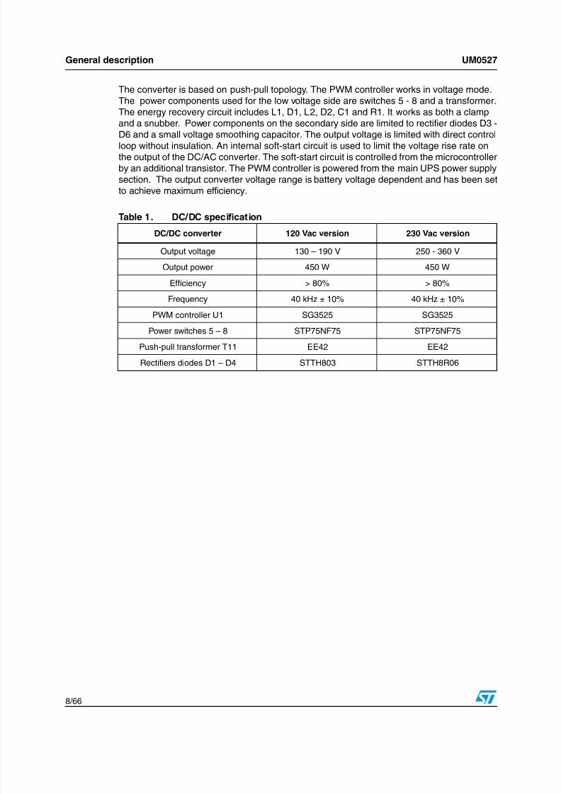
1.1.4 DC/DC converter module . . . . . . . . . . . . . . . . . . . . . . . . . . . . . . . . . . . . . 7
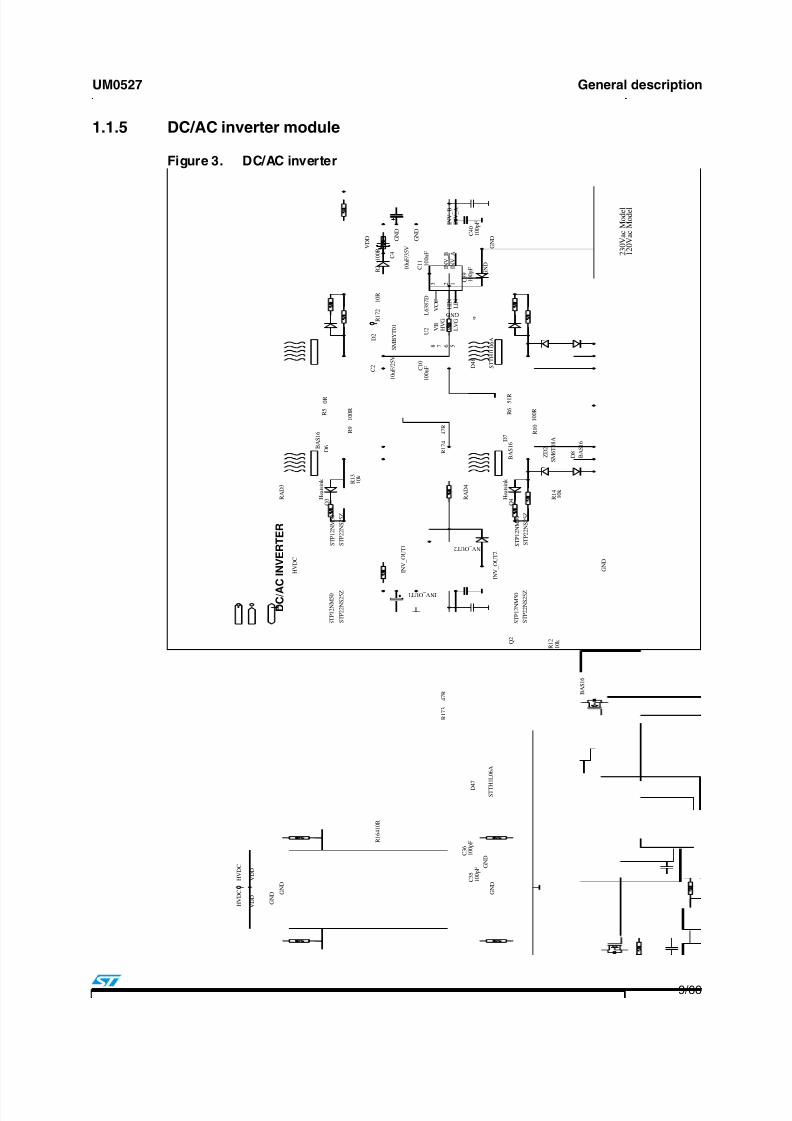
1.1.5 DC/AC inverter module . . . . . . . . . . . . . . . . . . . . . . . . . . . . . . . . . . . . . . 9
1.1.6 Power switches . . . . . . . . . . . . . . . . . . . . . . . . . . . . . . . . . . . . . . . . . . . 11
1.1.7 RFI/EMI filter . . . . . . . . . . . . . . . . . . . . . . . . . . . . . . . . . . . . . . . . . . . . . 12
1.1.8 Charger AC/DC . . . . . . . . . . . . . . . . . . . . . . . . . . . . . . . . . . . . . . . . . . . 13
1.1.9 Control unit . . . . . . . . . . . . . . . . . . . . . . . . . . . . . . . . . . . . . . . . . . . . . . 15
1.1.10 Power supply . . . . . . . . . . . . . . . . . . . . . . . . . . . . . . . . . . . . . . . . . . . . . 17
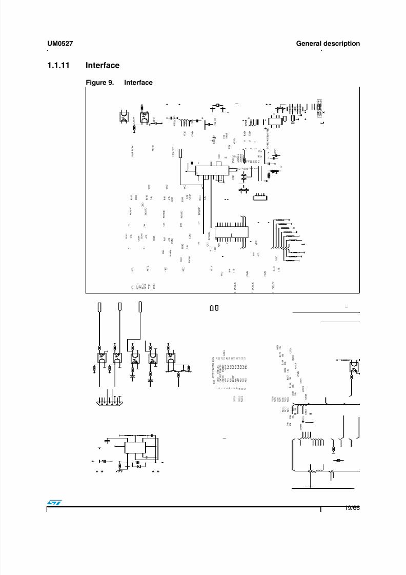
1.1.11 Interface . . . . . . . . . . . . . . . . . . . . . . . . . . . . . . . . . . . . . . . . . . . . . . . . . 19
1.1.12 Measurements: input voltage, input voltage phase, output current, inverteroutput voltage, battery voltage . . . . . . . . . . . . . . . . . . . . . . . . . . . . . . . . 21
1.1.13 Battery overcurrent protection . . . . . . . . . . . . . . . . . . . . . . . . . . . . . . . . 22
1.1.14 Mains protection . . . . . . . . . . . . . . . . . . . . . . . . . . . . . . . . . . . . . . . . . . 22
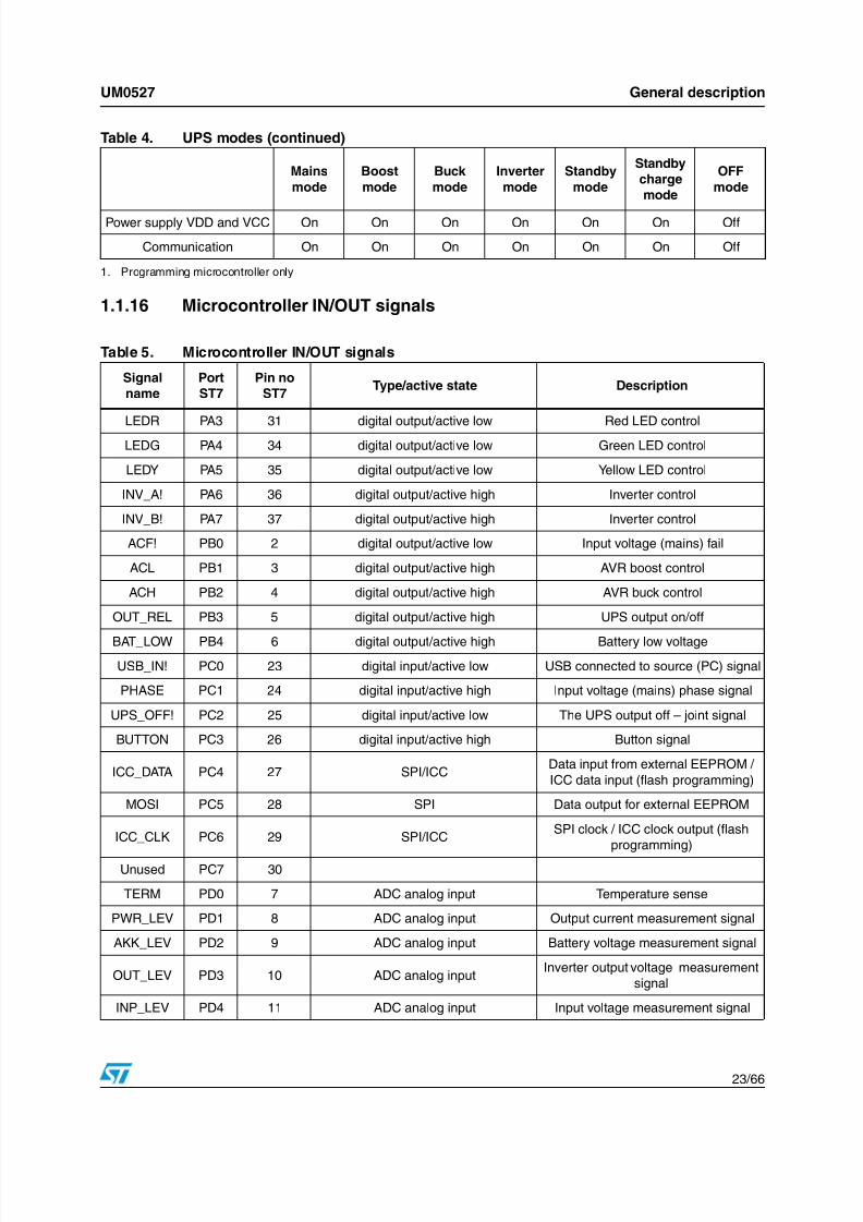
1.1.15 UPS modes . . . . . . . . . . . . . . . . . . . . . . . . . . . . . . . . . . . . . . . . . . . . . . 22
1.1.16 Microcontroller IN/OUT signals . . . . . . . . . . . . . . . . . . . . . . . . . . . . . . . 23
1.1.17 Signals functions table . . . . . . . . . . . . . . . . . . . . . . . . . . . . . . . . . . . . . . 24
1.1.18 Detailed description of mechanics . . . . . . . . . . . . . . . . . . . . . . . . . . . . . 25
1.2 Software architecture . . . . . . . . . . . . . . . . . . . . . . . . . . . . . . . . . . . . . . . . 26
1.2.1 Data models . . . . . . . . . . . . . . . . . . . . . . . . . . . . . . . . . . . . . . . . . . . . . . 26
1.2.2 Protocols . . . . . . . . . . . . . . . . . . . . . . . . . . . . . . . . . . . . . . . . . . . . . . . . 26
1.2.3 System architecture . . . . . . . . . . . . . . . . . . . . . . . . . . . . . . . . . . . . . . . . 27
1.2.4 Main loop . . . . . . . . . . . . . . . . . . . . . . . . . . . . . . . . . . . . . . . . . . . . . . . . 27
1.2.5 ADC . . . . . . . . . . . . . . . . . . . . . . . . . . . . . . . . . . . . . . . . . . . . . . . . . . . . 29
1.2.6 Communication . . . . . . . . . . . . . . . . . . . . . . . . . . . . . . . . . . . . . . . . . . . 30
1.2.7 SPI . . . . . . . . . . . . . . . . . . . . . . . . . . . . . . . . . . . . . . . . . . . . . . . . . . . . . 30
1.2.8 Keyboard . . . . . . . . . . . . . . . . . . . . . . . . . . . . . . . . . . . . . . . . . . . . . . . . 30
1.2.9 LEDs . . . . . . . . . . . . . . . . . . . . . . . . . . . . . . . . . . . . . . . . . . . . . . . . . . . 31
1.2.10 Charger . . . . . . . . . . . . . . . . . . . . . . . . . . . . . . . . . . . . . . . . . . . . . . . . . 31
1.2.11 Inverter . . . . . . . . . . . . . . . . . . . . . . . . . . . . . . . . . . . . . . . . . . . . . . . . . . 32
2 Technical description . . . . . . . . . . . . . . . . . . . . . . . . . . . . . . . . . . . . . . . 33
7/22/2019 UPSSG3525
http://slidepdf.com/reader/full/upssg3525 3/66
UM0527 Contents
3/66
2.1 Circuit diagram . . . . . . . . . . . . . . . . . . . . . . . . . . . . . . . . . . . . . . . . . . . . . 33
2.2 Layout . . . . . . . . . . . . . . . . . . . . . . . . . . . . . . . . . . . . . . . . . . . . . . . . . . . . 43
2.3 Assembly description . . . . . . . . . . . . . . . . . . . . . . . . . . . . . . . . . . . . . . . . 45
2.3.1 General . . . . . . . . . . . . . . . . . . . . . . . . . . . . . . . . . . . . . . . . . . . . . . . . . 45
2.3.2 Electrical . . . . . . . . . . . . . . . . . . . . . . . . . . . . . . . . . . . . . . . . . . . . . . . . 46
2.3.3 Mechanical . . . . . . . . . . . . . . . . . . . . . . . . . . . . . . . . . . . . . . . . . . . . . . . 46
2.4 Connectors . . . . . . . . . . . . . . . . . . . . . . . . . . . . . . . . . . . . . . . . . . . . . . . . 50
2.4.1 PCB: mains input . . . . . . . . . . . . . . . . . . . . . . . . . . . . . . . . . . . . . . . . . . 50
2.4.2 PCB: outlet output . . . . . . . . . . . . . . . . . . . . . . . . . . . . . . . . . . . . . . . . . 50
2.4.3 PCB: AVR transformer . . . . . . . . . . . . . . . . . . . . . . . . . . . . . . . . . . . . . . 50
2.4.4 PCB: battery . . . . . . . . . . . . . . . . . . . . . . . . . . . . . . . . . . . . . . . . . . . . . 51
2.4.5 PCB . . . . . . . . . . . . . . . . . . . . . . . . . . . . . . . . . . . . . . . . . . . . . . . . . . . . 51
2.4.6 PCB . . . . . . . . . . . . . . . . . . . . . . . . . . . . . . . . . . . . . . . . . . . . . . . . . . . . 51
2.4.7 PCB . . . . . . . . . . . . . . . . . . . . . . . . . . . . . . . . . . . . . . . . . . . . . . . . . . . . 51
2.5 Signalization description . . . . . . . . . . . . . . . . . . . . . . . . . . . . . . . . . . . . . 52
2.5.1 Indicators . . . . . . . . . . . . . . . . . . . . . . . . . . . . . . . . . . . . . . . . . . . . . . . . 52
2.5.2 Sound alarms . . . . . . . . . . . . . . . . . . . . . . . . . . . . . . . . . . . . . . . . . . . . . 52
2.6 Bill of material . . . . . . . . . . . . . . . . . . . . . . . . . . . . . . . . . . . . . . . . . . . . . . 52
2.6.1 Bill of material for 120 Vac version . . . . . . . . . . . . . . . . . . . . . . . . . . . . . 52
2.6.2 Bill of material for 230 Vac version . . . . . . . . . . . . . . . . . . . . . . . . . . . . . 58
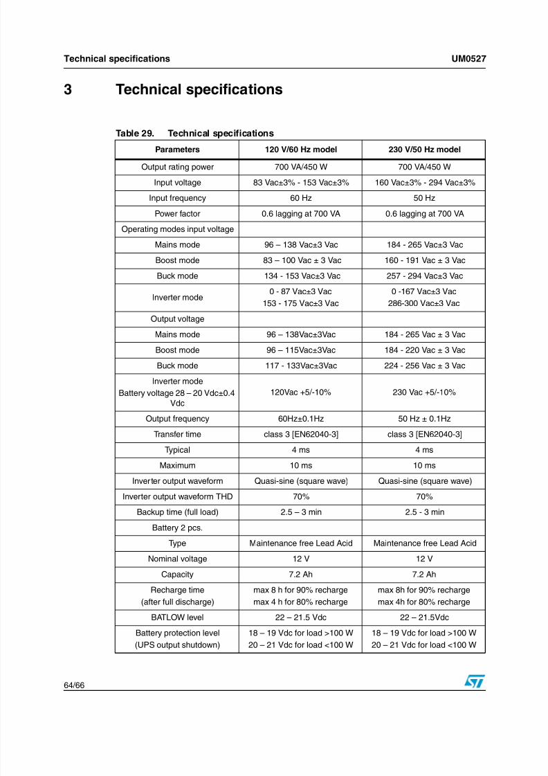
3 Technical specifications . . . . . . . . . . . . . . . . . . . . . . . . . . . . . . . . . . . . . 64
4 Revision history . . . . . . . . . . . . . . . . . . . . . . . . . . . . . . . . . . . . . . . . . . . 65

7/22/2019 UPSSG3525
http://slidepdf.com/reader/full/upssg3525 4/66
List of figures UM0527
4/66
List of figures
Figure 1. Block diagram . . . . . . . . . . . . . . . . . . . . . . . . . . . . . . . . . . . . . . . . . . . . . . . . . . . . . . . . . . . . 6Figure 2. DC/DC converter . . . . . . . . . . . . . . . . . . . . . . . . . . . . . . . . . . . . . . . . . . . . . . . . . . . . . . . . . 7Figure 3. DC/AC inverter . . . . . . . . . . . . . . . . . . . . . . . . . . . . . . . . . . . . . . . . . . . . . . . . . . . . . . . . . . . 9Figure 4. Power switches. . . . . . . . . . . . . . . . . . . . . . . . . . . . . . . . . . . . . . . . . . . . . . . . . . . . . . . . . . 11Figure 5. RFI/EMI filter. . . . . . . . . . . . . . . . . . . . . . . . . . . . . . . . . . . . . . . . . . . . . . . . . . . . . . . . . . . . 12Figure 6. AC/DC battery charger . . . . . . . . . . . . . . . . . . . . . . . . . . . . . . . . . . . . . . . . . . . . . . . . . . . . 13Figure 7. Control unit . . . . . . . . . . . . . . . . . . . . . . . . . . . . . . . . . . . . . . . . . . . . . . . . . . . . . . . . . . . . . 15Figure 8. Power supply . . . . . . . . . . . . . . . . . . . . . . . . . . . . . . . . . . . . . . . . . . . . . . . . . . . . . . . . . . . 17Figure 9. Interface . . . . . . . . . . . . . . . . . . . . . . . . . . . . . . . . . . . . . . . . . . . . . . . . . . . . . . . . . . . . . . . 19Figure 10. Measurements: input voltage, input voltage phase, output current, inverter output
voltage, battery voltage. . . . . . . . . . . . . . . . . . . . . . . . . . . . . . . . . . . . . . . . . . . . . . . . . . . . 21Figure 11. Battery overcurrent protection . . . . . . . . . . . . . . . . . . . . . . . . . . . . . . . . . . . . . . . . . . . . . . 22Figure 12. Main flowchart. . . . . . . . . . . . . . . . . . . . . . . . . . . . . . . . . . . . . . . . . . . . . . . . . . . . . . . . . . . 29
Figure 13. Circuit diagram . . . . . . . . . . . . . . . . . . . . . . . . . . . . . . . . . . . . . . . . . . . . . . . . . . . . . . . . . . 33Figure 14. DC/AC inverter . . . . . . . . . . . . . . . . . . . . . . . . . . . . . . . . . . . . . . . . . . . . . . . . . . . . . . . . . . 34Figure 15. DC/DC converter . . . . . . . . . . . . . . . . . . . . . . . . . . . . . . . . . . . . . . . . . . . . . . . . . . . . . . . . 35Figure 16. Control unit . . . . . . . . . . . . . . . . . . . . . . . . . . . . . . . . . . . . . . . . . . . . . . . . . . . . . . . . . . . . . 36Figure 17. Power switches. . . . . . . . . . . . . . . . . . . . . . . . . . . . . . . . . . . . . . . . . . . . . . . . . . . . . . . . . . 37Figure 18. AC/DC battery charger . . . . . . . . . . . . . . . . . . . . . . . . . . . . . . . . . . . . . . . . . . . . . . . . . . . . 38Figure 19. PC interface stage . . . . . . . . . . . . . . . . . . . . . . . . . . . . . . . . . . . . . . . . . . . . . . . . . . . . . . . 39Figure 20. Power supply . . . . . . . . . . . . . . . . . . . . . . . . . . . . . . . . . . . . . . . . . . . . . . . . . . . . . . . . . . . 40Figure 21. Measurement stages . . . . . . . . . . . . . . . . . . . . . . . . . . . . . . . . . . . . . . . . . . . . . . . . . . . . . 41Figure 22. RFI/EMI filter. . . . . . . . . . . . . . . . . . . . . . . . . . . . . . . . . . . . . . . . . . . . . . . . . . . . . . . . . . . . 42Figure 23. Battery overcurrent protection . . . . . . . . . . . . . . . . . . . . . . . . . . . . . . . . . . . . . . . . . . . . . . 42Figure 24. Top view . . . . . . . . . . . . . . . . . . . . . . . . . . . . . . . . . . . . . . . . . . . . . . . . . . . . . . . . . . . . . . . 43
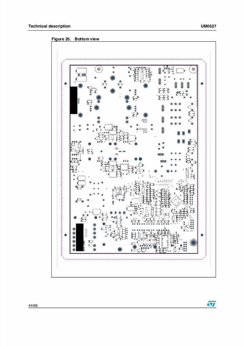
Figure 25. Bottom view . . . . . . . . . . . . . . . . . . . . . . . . . . . . . . . . . . . . . . . . . . . . . . . . . . . . . . . . . . . . 44Figure 26. Electrical connections . . . . . . . . . . . . . . . . . . . . . . . . . . . . . . . . . . . . . . . . . . . . . . . . . . . . . 46Figure 27. Mechanical view . . . . . . . . . . . . . . . . . . . . . . . . . . . . . . . . . . . . . . . . . . . . . . . . . . . . . . . . . 46Figure 28. UPS with assembled rear outlets . . . . . . . . . . . . . . . . . . . . . . . . . . . . . . . . . . . . . . . . . . . . 47Figure 29. UPS with front button and indicators . . . . . . . . . . . . . . . . . . . . . . . . . . . . . . . . . . . . . . . . . 47Figure 30. UPS with batteries and battery fuse . . . . . . . . . . . . . . . . . . . . . . . . . . . . . . . . . . . . . . . . . . 47Figure 31. UPS with battery fuse . . . . . . . . . . . . . . . . . . . . . . . . . . . . . . . . . . . . . . . . . . . . . . . . . . . . . 48Figure 32. UPS with AVR transformer . . . . . . . . . . . . . . . . . . . . . . . . . . . . . . . . . . . . . . . . . . . . . . . . . 48Figure 33. UPS with automatic fuse and power wires . . . . . . . . . . . . . . . . . . . . . . . . . . . . . . . . . . . . . 48Figure 34. UPS with motherboard . . . . . . . . . . . . . . . . . . . . . . . . . . . . . . . . . . . . . . . . . . . . . . . . . . . . 49Figure 35. UPS fully assembled. . . . . . . . . . . . . . . . . . . . . . . . . . . . . . . . . . . . . . . . . . . . . . . . . . . . . . 49Figure 36. UPS . . . . . . . . . . . . . . . . . . . . . . . . . . . . . . . . . . . . . . . . . . . . . . . . . . . . . . . . . . . . . . . . . . 50
7/22/2019 UPSSG3525
http://slidepdf.com/reader/full/upssg3525 5/66
UM0527 General description
5/66
1 General description
1.1 Hardware architecture
1.1.1 General realization
The UPS evaluation board is built in offline topology with AVR regulation of the mains boostand buck. The inverter module contains the push-pull DC/DC converter and the DC/ACoutput full-bridge generating quasi-sine waveform. The battery charger module is connectedat the output of the UPS and it also has the function of taking over the reactive power whichis present on the inverter during battery operation with reactive - resistive load.
The microcontroller controls all UPS functions. It monitors the mains parameters in order toensure the proper level of the output voltage. The microcontroller measurement parametersare input/output mains voltage and phase, output inverter voltage, battery voltage, outputcurrent and output power. The UPS has a built-in RS232, joint signals and USB interfaces
(USB for RS232 converter).

7/22/2019 UPSSG3525
http://slidepdf.com/reader/full/upssg3525 6/66
7/22/2019 UPSSG3525
http://slidepdf.com/reader/full/upssg3525 7/66
7/22/2019 UPSSG3525
http://slidepdf.com/reader/full/upssg3525 8/66
7/22/2019 UPSSG3525
http://slidepdf.com/reader/full/upssg3525 9/66

7/22/2019 UPSSG3525
http://slidepdf.com/reader/full/upssg3525 10/66
General description UM0527
10/66
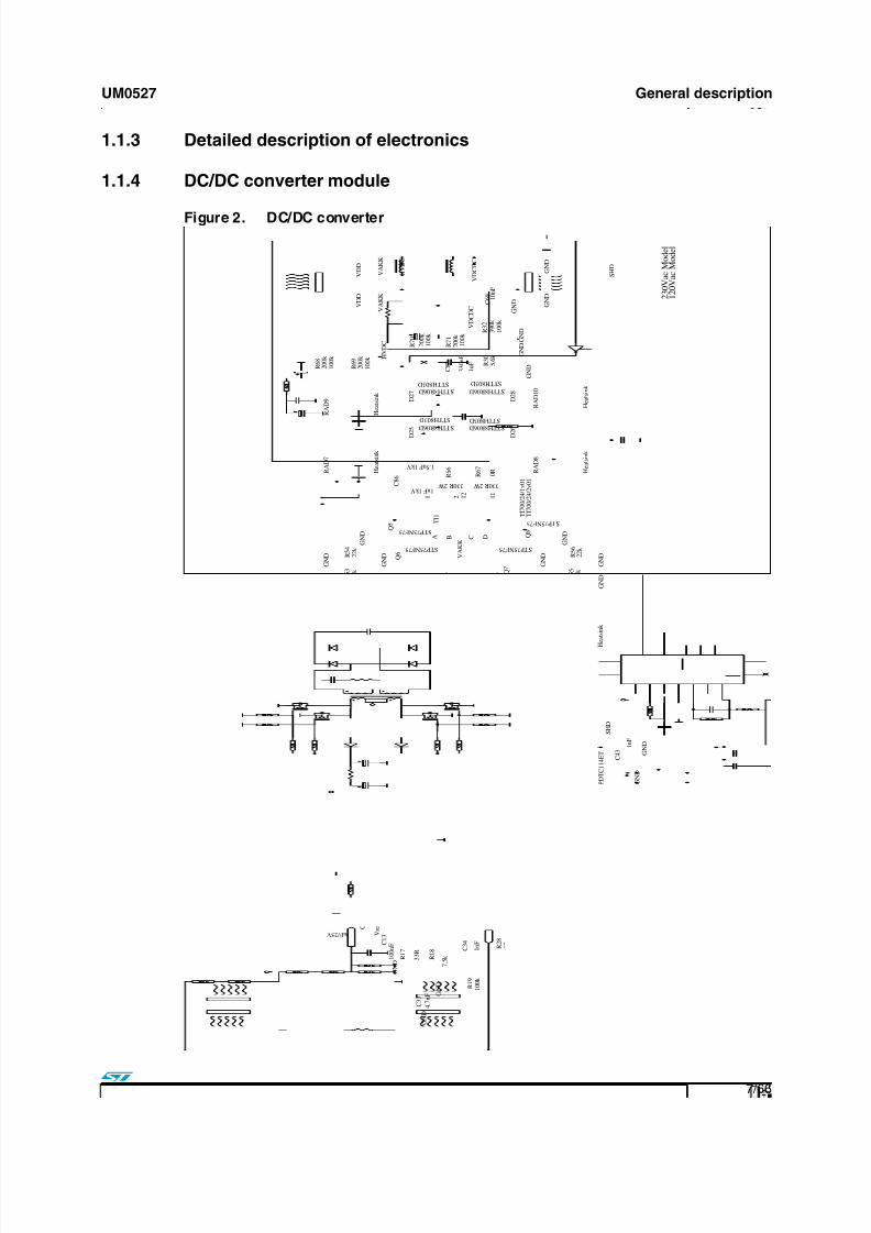
The DC/AC inverter was built in full-bridge topology. The output waveform is a quasi-sinewaveform. The inverter is controlled by the microcontroller across two PWM drivers whichswitch four power transistors. The high-side driver parts are supplied with the bootstrapcircuitry D1, C1 and D2, C2. The diodes D1 and D2 are high-voltage fast-recovery diodes.
Switching off all transistors is achieved with driver internal logic if both INV_A and INV_Bsignals are set high or low. There is no any additional overcurrent protection for bridgetransistors. Drivers are powered from the main UPS supply unit.
Table 2. DC/AC specification
DC/AC inverter 120 Vac version 230 Vac version
Output voltage RMS 120 Vac +5%/ -10% 230 Vac +5%/ -10%
Frequency (microcontroller
outputs)60 Hz ± 0.1 Hz 50 Hz ± 0.1Hz
Drivers U1, U2 L6387 L6387
Power switches Q1 – Q4 STP22NS25Z STP12NM50Bootstrap diode D1, D2 SMBYT01-400 SMBYT01-400
7/22/2019 UPSSG3525
http://slidepdf.com/reader/full/upssg3525 11/66

7/22/2019 UPSSG3525
http://slidepdf.com/reader/full/upssg3525 12/66
General description UM0527
12/66
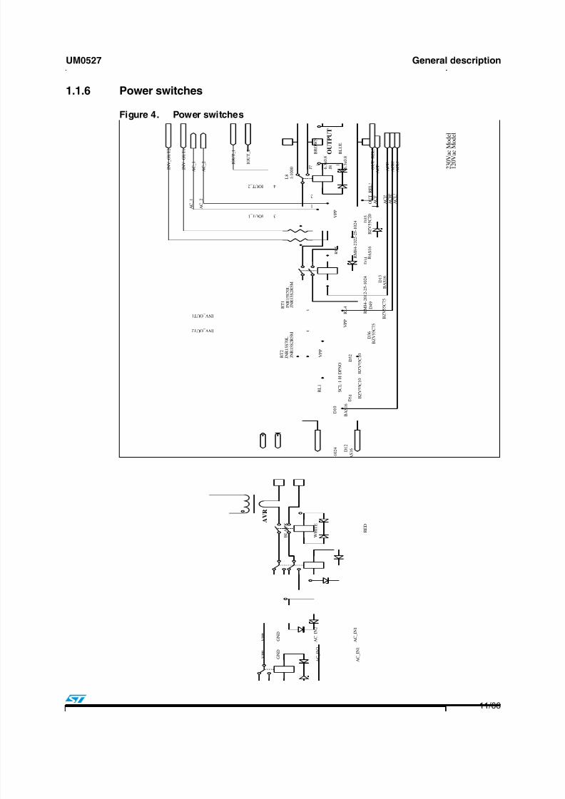
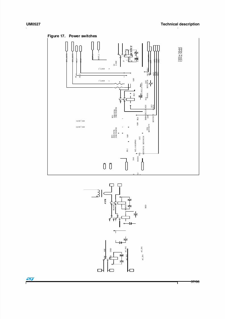
The power line contains:
two pole separation relays DPNO (RL1) (with 2 mm gap)
two relays DPDT (RL2, RL3)
two pole switching battery/mains relays DPDT (RL4)
two pole output on/off relays DPNO (RL5)
All relay coils are powered from the battery and charger voltage. The current transformer isused for monitoring UPS output current and power. The additional AVR boost/buckautotransformer has two sections: winding and output power 60VA. Relay coils arecontrolled by the microcontroller signals through an additional driver.
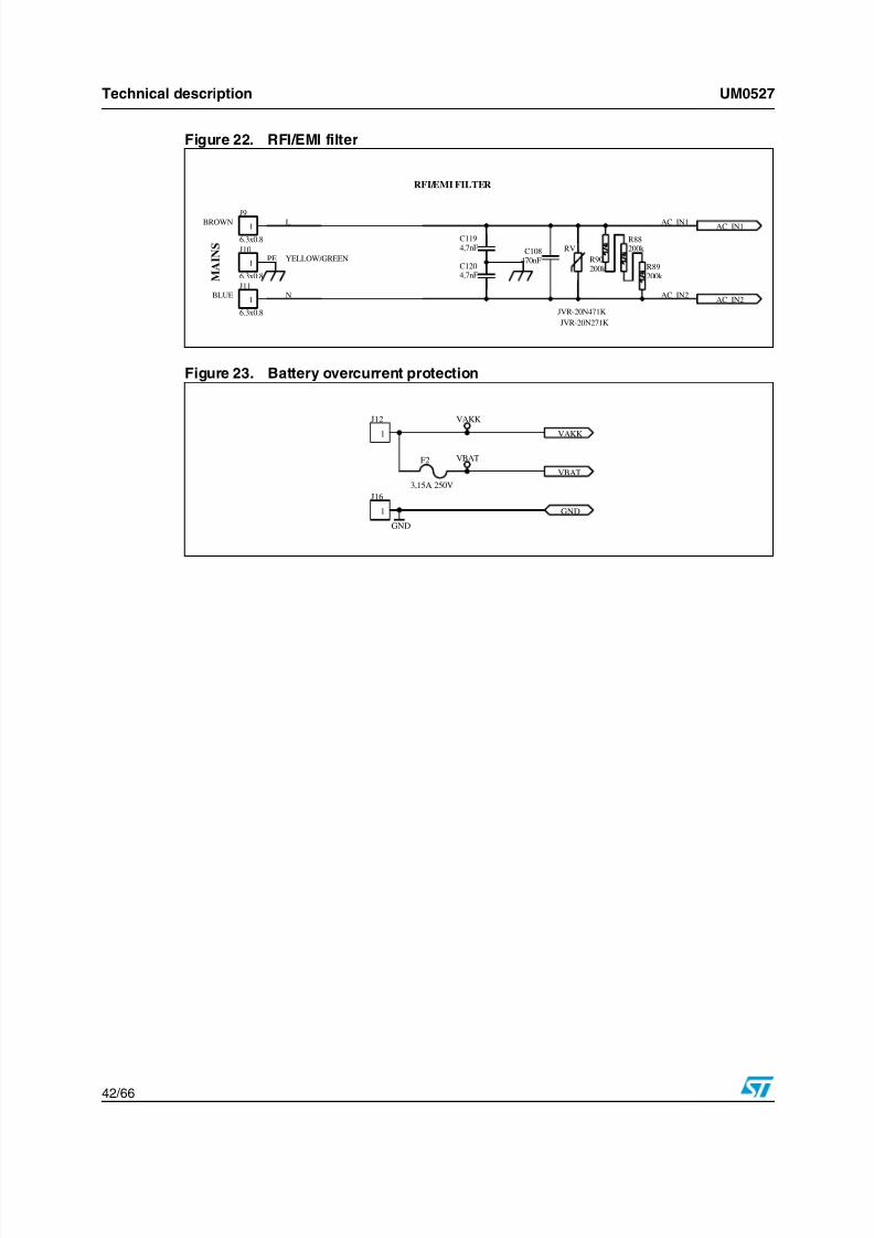
1.1.7 RFI/EMI filter
Figure 5. RFI/EMI filter
An additional EMI/RFI filter contains one X-type capacitor and a pair of Y-type capacitors.
L
N
C1204,7nF
AC_IN1
AC_IN2
PE R90200k
M A I N S
RFI/EMI FILTER
RV1
JVR-20N471K
R88200k
R89200k
JVR-20N271K
AC_IN1
AC_IN2
1
J9
6.3x0.8
1
J10
6.3x0.8
1
J11
6.3x0.8
C1194,7nF C108
470nF
BROWN
BLUE
YELLOW/GREEN

7/22/2019 UPSSG3525
http://slidepdf.com/reader/full/upssg3525 13/66
7/22/2019 UPSSG3525
http://slidepdf.com/reader/full/upssg3525 14/66
General description UM0527
14/66
The battery charger is used as a battery charger for the mains mode or as a reactive powerrecirculation circuit for the inverter mode. For both modes the charger output power isaccepted by the battery. The charger power converter is built in quasi-resonant flybackmode based on the controller L6565 with external power switch Q1 and output diode D1.
The PWM controller is powered from the main UPS supply module and from the auxiliarywinding on the flyback transformer. The transformer is designed with the ETD29 core. TheCHOFF signal is used to switch (Q2 and Q3 STP80PF55) charging modes by themicrocontroller. An additional output voltage loop limits open output charger voltage. Thecharger module also contains a battery overvoltage protection circuit with SCR TYN608 andvoltage reference TL431.
Table 3. Battery charger specifications
AC/DC converter 120 Vac version 230 Vac version
Max output voltage 29 Vdc ± 5%
Max output power 50 W
Efficiency >80%
Minimal switching frequency 100kHz ± 10%
Controller U1 L6565
Power switch Q11 STP5NK90Z
Transformer core ETD29
Rectifier diode D1 STPS8H100
Clamp diode D3 STTA106

7/22/2019 UPSSG3525
http://slidepdf.com/reader/full/upssg3525 15/66
UM0527 General description
15/66
1.1.9 Control unit
Figure 7. Control unit
G N D
G N D
C 8 8 2
2 p
F
C 8 9
2 2 p
F Y 1 1 6 M H z
N C 1
O N / O F F
B U Z Z E R
G N D V
C C P U
R X
T X
R S T !
P H A S
E
I N V _ A ! I N V _ B !
B U T T
O N
A C L
A C F !
P W R
_ L
E V
I N P
_ L E
V
A K K
_ L
E V
T X
R X
L 6
4 . 7
u H
L 5
4 . 7
u H
A C I
V C C P U
R 1 1 0
4 . 7
k
G N D
C 1 7
1 0 0 n
F
G N D
V D D
3
R E S
2
V S S 1
U 8
S T M 8 0 9 L
L 4
4 . 7
u H
L 3
4 . 7
u H
G N D
V C C P U
R S T !
R E S E T !
I C C_ C
L K
A C H
V A R E F
V S S A
O U T
_ R E L
R 9 1
1 0 k
R S T !
I C C
_ S E L
G N D
I C C_ D
A T A
I C P p r o g r a m m
i n g C
- F L A S H
1
1
2
2
B 1
B P T
- 1 4
R 1 2 0
2 . 2
k
V C C
A C I
R 1 1 3
3 . 3
k
R 1 1 4
3 . 3 k
C O M
9
1 B
1
1 C
1 6
2 B
2
2 C
1 5
3 B
3
3 C
1 4
4 B
4
4 C
1 3
5 B
5
5 C
1 2
6 B
6
6 C
1 1
7 B
7
7 C
1 0
8
E U 9
U L N 2 0 0 3 D
A C F !
I N V
_ A !
I N V
_ B !
O U T_ R
E L !
I N V
_ A
I N V
_ B
G N D
O U T
_ R E L
A C L !
A C L
A C H
V C C
A C H !
O U T
_ L E V
R 1 1 8
2 . 2
k
R 1 1 9
2 . 2
k
V C C V C C
I C C
_ D A T A
I C C
_ C L K
U P S_ O F F !
L E D R
L E D G
B A T
_ L O W
C H O F F
V C C
1 3 5 7
2 4 6 8
9
1 0
J 2 I D C 1 0
G N D
V C C
V C C
D 9
B A S 1 6
B U T T O N
Y A
R A
G A
R 1 0 9 3 3 0 R
R 1 0
7
3 3 0 R
S W
_ O N P
R 9 2
1 0 k
V C C
R 1 1 1
1 0 0 R
R 1 0 4
3 3 0 R
R 1 0 6
3 3 0 R
R 1 0 8
3 3 0 R
L E D R
L E D G
R 1 0 5
3 3 0 R
L E D Y
O S C 1 O S C 2
O S C 1
O S C 2
I C C _ S E L
V A R E F 1 3
V S S A 1 4
M C O / A I N 8 / P F 0 1 5
B E E P / P F 1 ( H S ) 1 6
O C M P 1 _ A / A I N 1 0 / P F 4 1 8
I C A P 1 _ A / P F 6 ( H S ) 1 9
E X T C L K _ A / P F 7 ( H S ) 2 0
A I N 1 2 / O C M P 2
_ B / P C 0
2 3
A I N 1 3 / O C M P 1
_ B / P C 1
2 4
I C A P 2
_ B / P C 2
2 5
I C A P 1
_ B / P C 3
2 6
I C C D A T A / M I S O / P C 4
2 7
A I N 1 4 / M O S I / P C 5
2 8
I C C C L K / S C K / P C 6
2 9
A I N 1 5 / S S / P C 7
3 0
P A 3 ( H S )
3 1
P A 4 ( H S ) 3 4
P A 6 ( H S ) 3 6
P A 7 ( H S ) 3 7
V p p / I C C S E L 3 8
R E S E T 3 9
V s s _ 2 4 0
O S C 2 4 1
O S C 1 4 2
V d d _ 2 4 3
P E 0 / T D O 4 4
P E 1 / R D I
1
P B 0
2
P B 3
5
P B 4 ( H S )
6
P D 0 / A I N 0
7
P D 1 / A I N 1
8
P B 1
3
P B 2
4
P D 2 / A I N 2
9
P D 3 / A I N 3
1 0
P D 4 / A I N 4
1 1
P D 5 / A I N 5 1 2
P F 2 ( H S ) 1 7
V d d _ 0 2 1
V s s _ 0 2 2
V d d
_ 1
3 2
V s s_
1
3 3
P A 5 ( H S ) 3 5
U 2 9
S T 7 2 F 3 2 4 B J 6 T 6
L E D Y
V D C D C
V C C P
U
G N D
G N D V C C P U
V C C P U
G N D
V A R E F V S S A
U S B_ I N !
S H D
T X D
R X D
I N V
_ A
I N V
_ B
A C L !
A C H !
A C F
O U T
_ R E L !
S W
_ O N P
B A T
_ L O W
U P S
_ O F F !
P H A S E
P W R
_ L E V
A K K
_ L E V
O U T
_ L E V
I N P
_ L E V
V D C D C
C H O F F
U S B
_ I N !
B A T
_ L O
W
U P S
_ O F F !
P H A S E
P W R
_ L E
V
A K K
_ L E
V
O U T
_ L E
V
I N P
_ L E V
V D C D C
C H O F F
U S B
_ I N !
S H D
S H D
1 3 5 7
2 4 6 8
9
1 0
J 1 I D C 1 0
G N D
V C C
R 3 8
1 k
R 3 7 1 k
S
1
Q
2
W
3
V S S
4
V C C
8
H O L D
7
C
6
D
5
U 1 0
M 9 5 0 2 0 W M N 6 P
M O S I
M O S I
I C C
_ C L K
S C K
I C C
_ D A T A
G N D
M I S O
V C C P U
V C C P U
R 3 9
4 . 7
k
R E S E T !
H O L D !
C S !
A C F 1 !
R 9 3
1 0 k
N C 1
G N D
A C I !
A C I !
B U Z Z E R
G N D
G N D
C S ! P
H A S E
I N V
_ B !
I N V
_ A !
U P S
_ O F F !
A K K
_ L E V
G N D
C 4 8
1 0 0 n F
C 3 7
1 n F
C 3 8
1 n
F
G N D
O N / O F F
R S T !
U S B
_ I N !
I C C_ C
L K
I C C_ S
E L
I C C_ D
A T A
B U T T O N
R X
T X
M O S I
G N D
G N D
G N D
G N D
G N D
G N D C
7 0
1 0 n F
C 7 1
1 0 n
F
C 7 3
1 n F
C 7 4
1 0 n F
C 7 6
1 0 n
F
C 7 7
1 0 n F
G N D
G N D
G N D
G N D
C 5 1
1 0 0 p F
C 5 2
1 0 0 p F
C 5 3
1 0 0 p F
C 5 4
1 0 0 p F
C 5 5
1 0 0 p F
C 5 6
1 0 0 p F G N D
G N D
G N D
V C C P U
C 1 6
1 0 0 n
F
O N / O F F
1 2 0 V a c M o d e l
2 3 0 V a c M o d e l
G N D
T X D
R X D
V C C P U
V C C
G N D
G N D
V C C
V C C P U
Q 1 5
M M B T A 4 2
R 8 6
4 . 7
k
R 8 7
1 0 k
G N D
A C F !
A C F !
A C F 1 !
A C F 1 !

7/22/2019 UPSSG3525
http://slidepdf.com/reader/full/upssg3525 16/66
General description UM0527
16/66
The control unit contains the main microcontroller ST72F324J6T6 - in the TQFP 44 10x10package with an ICP connector for programming, a reset STM809, a buffer ULN2003A fordriving signals and an external EEPROM with SPI interface. Analog signals are measuredwith an internal 10-bit A/D converter. Digital inputs / outputs are used to control internal and
external UPS signals. A thermistor is used to monitor internal UPS temperature.

7/22/2019 UPSSG3525
http://slidepdf.com/reader/full/upssg3525 17/66
7/22/2019 UPSSG3525
http://slidepdf.com/reader/full/upssg3525 18/66
7/22/2019 UPSSG3525
http://slidepdf.com/reader/full/upssg3525 19/66

7/22/2019 UPSSG3525
http://slidepdf.com/reader/full/upssg3525 20/66

7/22/2019 UPSSG3525
http://slidepdf.com/reader/full/upssg3525 21/66
7/22/2019 UPSSG3525
http://slidepdf.com/reader/full/upssg3525 22/66
General description UM0527
22/66
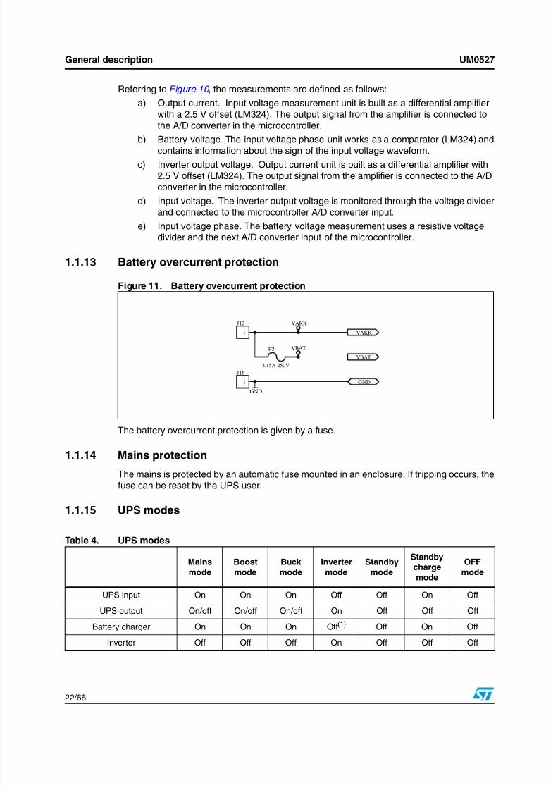
Referring to Figure 10 , the measurements are defined as follows:
a) Output current. Input voltage measurement unit is built as a differential amplifierwith a 2.5 V offset (LM324). The output signal from the amplifier is connected tothe A/D converter in the microcontroller.
b) Battery voltage. The input voltage phase unit works as a comparator (LM324) andcontains information about the sign of the input voltage waveform.
c) Inverter output voltage. Output current unit is built as a differential amplifier with2.5 V offset (LM324). The output signal from the amplifier is connected to the A/Dconverter in the microcontroller.
d) Input voltage. The inverter output voltage is monitored through the voltage dividerand connected to the microcontroller A/D converter input.
e) Input voltage phase. The battery voltage measurement uses a resistive voltagedivider and the next A/D converter input of the microcontroller.
1.1.13 Battery overcurrent protection
Figure 11. Battery overcurrent protection
The battery overcurrent protection is given by a fuse.
1.1.14 Mains protection
The mains is protected by an automatic fuse mounted in an enclosure. If tr ipping occurs, thefuse can be reset by the UPS user.
1.1.15 UPS modes
F2
3,15A 250V
VAKK
VBAT
GND
1
J12
1
J16
VAKK
VBAT
GND
Table 4. UPS modes
Mains
mode
Boost
mode
Buck
mode
Inverter
mode
Standby
mode
Standbycharge
mode
OFF
mode
UPS input On On On Off Off On Off
UPS output On/off On/off On/off On Off Off Off
Battery charger On On On Off(1) Off On Off
Inverter Off Off Off On Off Off Off
7/22/2019 UPSSG3525
http://slidepdf.com/reader/full/upssg3525 23/66
7/22/2019 UPSSG3525
http://slidepdf.com/reader/full/upssg3525 24/66
General description UM0527
24/66
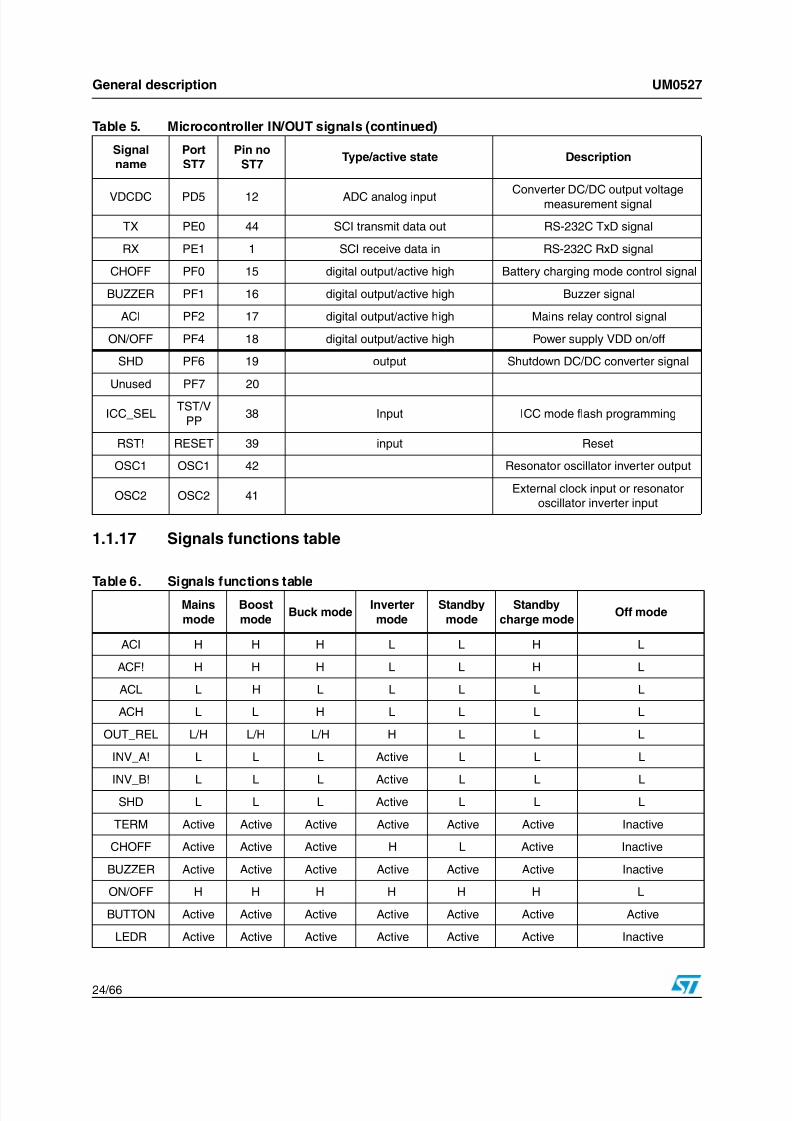
1.1.17 Signals functions table
VDCDC PD5 12 ADC analog inputConverter DC/DC output voltage
measurement signal
TX PE0 44 SCI transmit data out RS-232C TxD signal
RX PE1 1 SCI receive data in RS-232C RxD signal
CHOFF PF0 15 digital output/active high Battery charging mode control signal
BUZZER PF1 16 digital output/active high Buzzer signal
ACI PF2 17 digital output/active high Mains relay control signal
ON/OFF PF4 18 digital output/active high Power supply VDD on/off
SHD PF6 19 output Shutdown DC/DC converter signal
Unused PF7 20
ICC_SELTST/V
PP38 Input ICC mode flash programming
RST! RESET 39 input Reset
OSC1 OSC1 42 Resonator oscillator inverter output
OSC2 OSC2 41External clock input or resonator
oscillator inverter input
Table 5. Microcontroller IN/OUT signals (continued)
Signal
name
Port
ST7
Pin no
ST7Type/active state Description
Table 6. Signals functions table
Mains
mode
Boost
modeBuck mode
Inverter
mode
Standby
mode
Standby
charge modeOff mode
ACI H H H L L H L
ACF! H H H L L H L
ACL L H L L L L L
ACH L L H L L L L
OUT_REL L/H L/H L/H H L L L
INV_A! L L L Active L L L
INV_B! L L L Active L L LSHD L L L Active L L L
TERM Active Active Active Active Active Active Inactive
CHOFF Active Active Active H L Active Inactive
BUZZER Active Active Active Active Active Active Inactive
ON/OFF H H H H H H L
BUTTON Active Active Active Active Active Active Active
LEDR Active Active Active Active Active Active Inactive

7/22/2019 UPSSG3525
http://slidepdf.com/reader/full/upssg3525 25/66
UM0527 General description
25/66
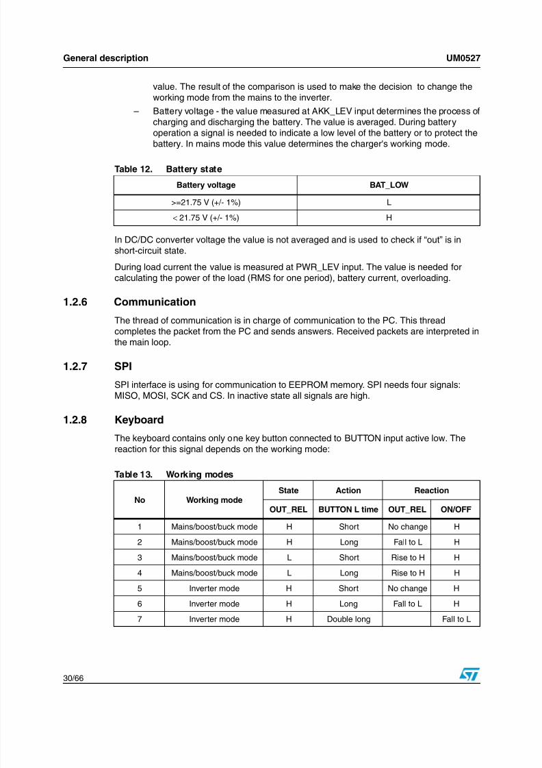
1.1.18 Detailed description of mechanics
The standard enclosure dimensions are as follows:
Main PCB:
– Dimensions: 230 x 160 mm
– Type: double-sided GE (glass - epoxy), FR4 with SMOBC
LEDs and button PCB:
– Dimensions: 80 x 25 mm
– Type: single-sided GE (glass - epoxy), FR4 with SMOBC
LEDG Active Active Active Active Active Active Inactive
LEDY Active Active Active Active Active Active Inactive
TX Active Active Active Active Active Active Inactive
RX Active Active Active Active Active Active Inactive
USB_IN! H or L H or L H or L H or L H or L H or L L
BAT_LOW L L L H or L H or L L L
UPS_OFF! H or L H or L H or L H or L H H L
MOSI Active Active Active Active Active Active Inactive
ICC_SEL L L L L L L Active(1)
ICC_DATA/ MISO
L/ Active L/ Active L/ Active L/ Active L/ Active L/ Active Active(1) / Inactive
ICC_CLK/
SCKL/ Active L/ Active L/ Active L/ Active L/ Active L/ Active
Active(1) /
Inactive
PHASE Active Active Active Active Active Active Inactive
INP_LEV Active Active Active Active Active Active Inactive
OUT_LEV Inactive Inactive Inactive Active Inactive Inactive Inactive
PWR_LEV Active Active Active Active Inactive Inactive Inactive
1. Programming microcontroller only
H - high level +5 Vdc
L - low level 0 Vdc
Active - active signal
Inactive - inactive signal
Table 6. Signals functions table (continued)
Mains
mode
Boost
modeBuck mode
Inverter
mode
Standby
mode
Standby
charge modeOff mode

7/22/2019 UPSSG3525
http://slidepdf.com/reader/full/upssg3525 26/66
7/22/2019 UPSSG3525
http://slidepdf.com/reader/full/upssg3525 27/66
UM0527 General description
27/66
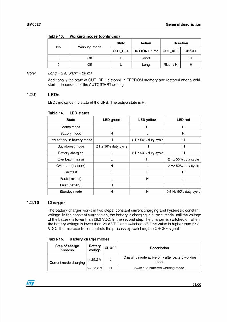
1.2.3 System architecture
1.2.4 Main loop
The UPS works in 7 modes:
– Inverter mode - if the mains voltage is lower than 167 VAC RMS(87 for USversion) or higher than 286 VAC RMS(153 for US version) the inverter is switchedon. At outputs INV_B and INV_A, a PWM signal 50 Hz (60 for US version) with40% or less duty cycles (depends on DC/DC output voltage) is generated. Ininverter mode the ACF signal is switched on. If the mains voltage returns to thecorrect value (167 - 286 VAC or 87 - 153 VAC for US version), the PWM signal is
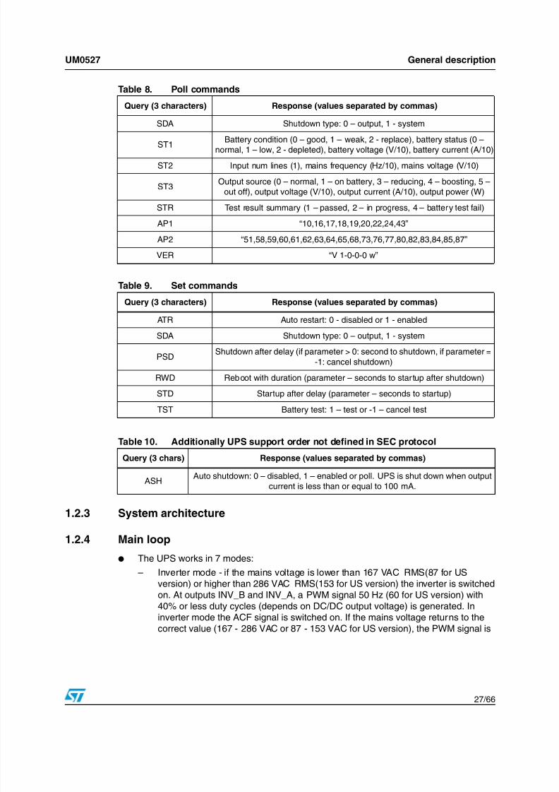
SDA Shutdown type: 0 – output, 1 - system
ST1 Battery condition (0 – good, 1 – weak, 2 - replace), battery status (0 –normal, 1 – low, 2 - depleted), battery voltage (V/10), battery current (A/10)
ST2 Input num lines (1), mains frequency (Hz/10), mains voltage (V/10)
ST3Output source (0 – normal, 1 – on battery, 3 – reducing, 4 – boosting, 5 –
out off), output voltage (V/10), output current (A/10), output power (W)
STR Test result summary (1 – passed, 2 – in progress, 4 – battery test fail)
AP1 “10,16,17,18,19,20,22,24,43”
AP2 “51,58,59,60,61,62,63,64,65,68,73,76,77,80,82,83,84,85,87”
VER “V 1-0-0-0 w”
Table 9. Set commands
Query (3 characters) Response (values separated by commas)
ATR Auto restart: 0 - disabled or 1 - enabled
SDA Shutdown type: 0 – output, 1 - system
PSDShutdown after delay (if parameter > 0: second to shutdown, if parameter =
-1: cancel shutdown)
RWD Reboot with duration (parameter – seconds to startup after shutdown)
STD Startup after delay (parameter – seconds to startup)
TST Battery test: 1 – test or -1 – cancel test
Table 10. Additionally UPS support order not defined in SEC protocol
Query (3 chars) Response (values separated by commas)
ASHAuto shutdown: 0 – disabled, 1 – enabled or poll. UPS is shut down when output
current is less than or equal to 100 mA.
Table 8. Poll commands
Query (3 characters) Response (values separated by commas)

7/22/2019 UPSSG3525
http://slidepdf.com/reader/full/upssg3525 28/66
General description UM0527
28/66
synchronized with the mains, the ACF! signal is set to low and the inverter isswitched off.
– Mains mode - in this mode the battery charger is switched on and the UPS issupplied from the mains. The inverter is switched off (INV_A and INV_B are in low
state), and ACF! is high.– Buck mode - in this mode the battery charger is switched on and the UPS is
supplied from the mains. The ACH signal is switched on, the inverter is switchedoff, ACF! is high and the ACL signal is in low state.
– Boost mode - in this mode the battery charger is switched on and the UPS issupplied from the mains. The ACL signal is switched on, the inverter is switchedoff, ACF! is high and the ACH signal is in low state.
– Standby mode - in this mode the battery charger is switched off and the UPS issupplied from the battery. ACH and ACL are in low state, ACF! is low, CHOFF ishigh, and the inverter is switched off.
– Standby charge mode - the UPS is in this state when the mains is lower than thelow level boost mode. ACH and ACL are in low state, ACF! is high, CHOFF is low,and the inverter is switched off.
– OFF mode - the UPS in this mode is totally switched off. This state is availably onlyin battery mode after pressing the on/off key longer than 4 seconds.
Additionally the UPS tests the battery. The battery test is done by switching to the invertermode. During the test the MCU measures UPS output load and battery voltage. If thebattery voltage during the test falls below the limit, the battery is failing. The value of the limitdepends on time and load current. The test can be forced by the user with a PC. The batterycondition can by checked after switching to the inverter mode without forcing the test. A loadis necessary to test the battery.
Table 11. Signal state in different modes
Work mode INV_A INV_B ACH ACL ACF! CHOFF SHD
Inverter mode
50 Hz (60 for US
version) PWM
signal (less than
40% duty cycle)
50 Hz (60 for US
version) PWM
signal (less than
40% duty cycle)
L L L L
Signal is switched to
L after rising edge
INV_A or INV_B and
switched to H before
falling edge INV_A
or INV_B.
Mains mode L L L L H
Depends on
battery
voltage
H
Buck mode L L L H H H
Boost mode L L H L H H
Standby mode L L L L L H H
Standby charge
modeL L L L H
Depends on
battery
voltage
H
Off mode L L L L H L L

7/22/2019 UPSSG3525
http://slidepdf.com/reader/full/upssg3525 29/66
UM0527 General description
29/66
Figure 12. Main flowchart
1.2.5 ADCThe ADC thread measures values as described below:
Mains voltage - the voltage measured at INP_LEV is needed for calculating thefollowing values:
– RMS - true RMS main voltage which determines the working mode of the UPS:mains mode, buck mode, boost mode or inverter mode. This value is calculated forone period of input voltage.
– SAMPLE - actual sample voltage which is the value needed for calculating RMS.Additionally this value is needed to compare with the predicted value of the mains
7/22/2019 UPSSG3525
http://slidepdf.com/reader/full/upssg3525 30/66
7/22/2019 UPSSG3525
http://slidepdf.com/reader/full/upssg3525 31/66
7/22/2019 UPSSG3525
http://slidepdf.com/reader/full/upssg3525 32/66

7/22/2019 UPSSG3525
http://slidepdf.com/reader/full/upssg3525 33/66

7/22/2019 UPSSG3525
http://slidepdf.com/reader/full/upssg3525 34/66
Technical description UM0527
34/66
Figure 14. DC/AC inverter
D C
/ A C I N V E R T E R
H V D C
G N D
D 1
S M B Y T 0 1
V D D
R 1 2
1 0 k
R 1 1
1 0 k
R 7
1 0 0 R
C 1
1 0 u F
/ 2 5 V
R 1 4
1 0 k
R 1 3
1 0 k
L I N
1
H I N
2
V C C
3
G N D 4
L V G
5
V O
6
H V G
7
V B
8
U 1
L 6 3 8 7 D
Q 1
S T P 1 2 N M
5 0
Q 2
S T P 1 2 N M 5 0
Q 4
S T P 1 2 N M 5 0
Q 3
S T P 1 2 N M 5 0
D 2
S M B Y T 0 1
V D D
C 2
1 0 u F
/ 2 5 V
L I N
1
H I N
2
V C C
3
G N D 4
L V G
5
V O
6
H V G
7
V B
8
U 2
L 6 3 8 7 D
I N V
_ B
I N V
_ A
I N V
_ A
I N V
_ B
I N V
_ O U T 2
I N V
_ O U T 1
R 1 1 0 0 R
R 2
1 0 0 R
C 8
1 0 0 n
F
C 1 0
1 0 0 n F
C 9 1
0 0 n F
C 1 1
1 0 0 n F
G N
D
G N
D
G N D
G N D
R 3
0 R
D 3
B A S 1 6
R 8
1 0 0 R
R 4
5 1 R
D 4
B A S 1 6
R 1 0 1
0 0 R R
6
5 1 R
D 7
B A S 1 6
R 9 1
0 0 R
R 5
0 R
D 6 B
A S 1 6
Z D 1
S M 6 T 1 8 A
D 5
B A S 1 6
Z D 2
S M 6 T 1 8 A
D 8
B A S 1 6
S T P 2 2 N S 2 5 Z
S T P 2 2 N S 2 5 Z
S T P 2 2 N S 2 5 Z
S T P 2 2 N S 2 5 Z
R A D 1
H e a t s i n
k
R A D 3
H e a t s i n
k
R A D 2
H e a t s i n
k
R A D 4
H e a t s i n
k
C 4
1 0 u
F / 3 5 V
C 3
1 0 u F
/ 3 5 V
I N V
_ A
I N V
_ B
I N V
_ A
I N V
_ B
I N V _ O U T 1
I N V _ O U T 2
1 2 0 V a
c M o
d e l
2 3 0 V a
c M o
d e l
H V D C
G N D G
N D
H V D C
V D D
V D D
R 1 7 3
4 7 R
R 1 6 4 1 0 R
D 4 7
S T T H 1 L 0 6 A
D 4 8
S T T H 1 L 0 6 A
R 1 7 4
4 7 R
R 1 7 2
1 0 R
C 3 6
1 0 0 p
F
G N D
C 3 5
1 0 0 p
F
G N D
C 3 9
1 0 0 p
F
C 4 0
1 0 0 p F
G N D
G N D

7/22/2019 UPSSG3525
http://slidepdf.com/reader/full/upssg3525 35/66

7/22/2019 UPSSG3525
http://slidepdf.com/reader/full/upssg3525 36/66
7/22/2019 UPSSG3525
http://slidepdf.com/reader/full/upssg3525 37/66
UM0527 Technical description
37/66
Figure 17. Power switches
1 J 8 6 .
3 x
0 . 8
1 J 7 6 .
3 x
0 . 8
1
2
3
4
L 8
1 : 1 0 0 0
I O U T _ 2
I O U T _ 1
R L 5
R M 8 4
- 2 0 2 2
- 2 5
- 1 0 2 4
R L 2
R M 8 5 - 2 0 1 1
- 2 5 - 1
0 2 4
R L 3
R M 8 5
- 2 0 1 1
- 2 5 - 1
0 2 4
1 J 5
6 . 3
x 0
. 8 1
J 4
6 . 3
x 0
. 8
D 1 2
B A S 1 6
D 3 4
B Z V 5 5 C 2 0
D 3 3
B Z V 5 5 C 2 0
D 1 1 B
A S 1 6
V P P
V P P
V P P
A C L !
A C H !
D 3 5
B Z V 5 5 C 2 0
D 1 4 B
A S 1 6
O U T
_ R E L !
R L 4
R M 8 4
- 2 0 1 2
- 2 5
- 1 0 2 4
I N V _ O U T 1
I N V _ O U T 2
1 J 6
6 . 3
x 0
. 8
D 1 3
B A S 1 6
D 3 6
B Z V 5 5 C 7 5 V
P P
D 1 0
B A S 1 6
D 3 1
B Z V 5 5 C 1 0
V P P
A C F
O
U T P U T
I O U T
_ 2
I O U T
_ 1
O U T
_ R E
L !
A C H !
A C L !
A C F
A V R
A C
_ 1
A C
_ 2
A C
_ I N 1
A C
_ I N 2
R L 1
S C L
- 1 - H - D
P N O
A C I !
A C I !
D 3 2
B Z V 5 5 C 1 0
1 2 0 V a c
M o
d e l
2 3 0 V a c
M o
d e l
I N V
_ O U T 2
I N V
_ O U T 1
A C
_ I N 2
A C
_ I N 1
V P P
G N D
G N D
V P P
A C
_ 1
A C
_ 2
t R T 1
J N R 1 5 S 7
0 L
t
R T 2
J N R 1 5 S 7 0 L
J N R 1 5 S 2 R 5 M
J N R 1 5 S 2 R 5 M
D 4 9
B Z V 5 5 C 7 5
B L A C K
W H I T E
R E D
B R O W N
B L U E

7/22/2019 UPSSG3525
http://slidepdf.com/reader/full/upssg3525 38/66
Technical description UM0527
38/66
Figure 18. AC/DC battery charger
A C / D C B A T T E R Y C H
A R G E R
G N D
R 9 4
1 0 k
C 1 0 1
1 0 0 0 u F / 5 0 V
G N D
D 3 8
S T P S 8 H 1 0 0 D
D 1 6
B A S 1 6
G N D
C 9 9
1 n F 5 0 0 V
R 6 4 1 0 R
R 1 6
1 0 k
G N
D
C 2 0 1 0 0 n F
G N
D
L 1 1
1 0 u H / 3 A
C 1 9
1 0 0 n F
G N D
+ V O
U T
G N D
1 4
1 2
1 0
6 7 3 2
9
`
8 1 1
1 3
T 1
T I 5 0 / 3 0 v 0 2
R 2 0
1 0 0 k
V D D
F 1
1 , 2
5 A
C 9 6
1 0 0 n F X 2
V F F
3
V D D 8
Z C D 5
V F B 1
C O M P 2
G D
7
C S
4
G N D 6
U 1 1
L 6 5 6 5
G N D
G N D
R 1 3 4
1 6 k
R 1 3 2
7 5 0 k
R 1 3 5
4 3 k
R 9 5
1 0 k
G N D
R 1 3 8 3 3 k
V B A T M A X +
2 8
. 2 V
6 1
8
7
2 3
U 1 2
T L 4 3 1 C D
R 1 3 6
3 9 k
R 1 1 5
3 . 3
k
R 5 7
2 2 k
G N D
R 1 3 9
5 . 6
k
R 1 4 0
1 8 0 R
Q 1 2
B C 8 5 7 B
O v e r v o l t a g e P r o t e c t i o n 3 2 V
T H 1
T Y N 6 0 8
G N D
2
1
3
4
B R 1
K B U 6 0 5
C o n t r o l v o l t a g e o u t p u t
C u r r e n t M o d e C h a r g i n g
V o l t a g e M o d e
C h a r g i n g
P o u t ( m a x ) = 5 0 W
C h a r g e r O u t p u t
V B A T
R 1 2 9 1 0 R
G N D
G N D
Q 1 1
S T P 5 N K 9 0 Z
R 1 3 3 3 3 R R 1 5 1 0 k
G N D
C H O F F
V B A T M I N + 2 6
. 8 V
R 1 2 3
1 0 0 k
D 3 7
S T T H 1 R 0 6
R 1 2 7
1 2 0 k 3 W
C 9 7
6 8 0 p F 1 6 0 0 V
A C
_ 2
A C
_ 1
Q 1 0
S T P 8 0 P F 5 5
U 6
P D T C 1 1 4 E T
+ V O U T
Z D 3
B Z X 8 4 C 1 2
C 1 0 0
1 0 0 u F / 5 0 V
G N D
R A D 1 1
H e a t s i n k
2 A
R 1 3 1
7 5 0 k
R 1 3 0
7 5 0 k
G
N D
R 6 3
1 0 R
R 1 2 4
1 0 0 k
R 1 2 5
1 0 0 k
R 1 2 6
1 0 0 k
G N D
C 9 8
4 7 u F / 5 0 V
C 2 1 1 0 0 n F
G N D
G N D
C 1 0 2
1 0 0 0 u F / 5 0 V
R 1 2 2 1 0 0 k
G N D
R 6 5 1 0 R
R 1 2 8
1 2 0 k 3 W
R A D 1 2
H e a t s i n k
R 1 3 7
0 . 6 8 R 2 W
L 9
1 0 u H / 3 A
L 1 0
1 0 u H / 3 A
C 1 8 1 0 0 n F
C 4 9
1 n F
C 7 9
1 0 n F
C 9 5
4 7 n F X 2
1 2 0 V a c
M o
d e l
2 3 0 V a c
M o
d e l
C H O F F
A C
_ 1
A C
_ 2
D 1 5
B A S 1 6
D 1 7
B A S 1 6
Q 9
S T P 8 0 P F 5 5
V B A T
G N D
+ V O U T
G N D
+ V O U T
V D D
V D D
R 5 2
4 . 7
R 3 W
C 4 4
4 7 n F X
2
7/22/2019 UPSSG3525
http://slidepdf.com/reader/full/upssg3525 39/66
UM0527 Technical description
39/66
Figure 19. PC interface stage
C O M C
1 0 3
2 2 u F / 3 5 V
V +
C O M
R 1 2 1
2 . 2
k
C 1 0 9
2 . 2
u F / 5 0 V
T R I G
2
Q
3
R
4
C V o l t
5
T H R
6
D I S
7
V C C 8
G N D 1
U 1 4
T S 5 5 5 C D T
C O M
C 2 5 1
0 0 n F
C 2 3
1 0 0 n F
C 5
1 0 u F / 3 5 V
C 2 2
1 0 0 n F
R 9 7 1
0 k
R 4 1
4 . 7
k
V -
D 1 8
B A S 1 6
C O M
C O M
V P C
V P C
O F F
O F F
1 6 2 7 3 8 4 9 5
J 1 4
U 2 1
P C 8 1
7 C
U 1 9
P C 8 1 7 C
U 2 0
P C 8 1 7 C
D 1 9
B A S 1 6
R 4 5
4 . 7
k
R 1 4 8
2 . 4
k
R 1 4 7
8 2 0 R
B T L
A C F L
O F F
R 1 4 6
4 . 7
k
R 1 4 5
4 . 7
k
R 4 8
4 . 7
k
U 2 2
P C 8 1
7 C
U 2 3
P C 8 1 7 C
R 1 1 2
1 0 0 R
R 9 9
2 0 k
R 1 4 4
2 . 2
k
R 1 4 9 6
. 8 k
D 2 0
B A S 1 6
R 1 4 2
3 . 3
k V
- V +
T X D 1
R X D 1
C O M
V C C
V C C
G N D
V C C
C O M
C O M
C O M
V +
V +
V C C
C O M
V P C
B A T
_ L O W
A C F 1 !
U P S
_ O F
F !
R X D
T X D
Q 1 3
B C 8 4 6 B
Q 1 4
B C 8 5 7 B
G N D
A C F 1 !
B A T
_ L O W
U P S
_ O F F !
R X D
T X D
G N D
T x D
_ U S B
G N D 1
G N D 1
C 9 2
2 2 p F
C 9 1
2 2 p F
Y 2
2 4 M H z
U S B D M
G N D 1
1 2 3 4
J 1 3 U
S B - B
G N D 1
C 2 4
1 0 0 n F
R 4 3
4 . 7
k
G N D 1
T x D
_ U S B
U S B
R x D
_ U S B
O S C O U T
O S C I N
R S T
_ U S B
U S B D P
U S B V C C
+ 5 V
_ U S B
O S C O U T
O S C I N
+ 5 V
_ U S B
U S B D M
U S B D P
I C C C L K
I C C D A T A
V P P
_ U S B
C 6
1 0 u F / 3 5 V
I C C D A T A
I C C C L K
R S T
_ U S B
V P P
_ U S B
G N D 1
+ 5 V
_ U S B
I C C D A T A
I C C C L K
R 9 8
1 0 k
V P P
_ U S B
G N D 1
U S B V C C
R 1 4 1
1 . 5
k
U S B
S o c k e t
C 5 7
1 0 0 p F
C 5 8 1 0 0 p F
C 8 0
1 0 n F G
N D 1
R S T
_ U S B
R x D
_ U S B
I C P
R X D 1
T X D 1
A C F L
B T L
O F F
U 1 7
P C 8 1 7 C
U 1 8
P C 8 1 7 C
R 4 4
4
. 7 k
R 1 4 3
4 . 3
k
+ 5 V
_ U S B
G N D 1
G N D
R 4 7
4 . 7
k
V C C
U 1 6
P C 8 1 7 C
R 4 2
4 . 7
k G N D 1
+ 5 V
_ U S B
R 4 6
4 . 7
k
G N D
V C C
G N D
G N D
+ 5 V
_ U S B
I N H
6
A D D R A
1 1
A D D R C
9
A 1
1 2
A 2
1 3
B 1
2
B 2
1
C 1
5
C 2
3
C
4
A
1 4
B
1 5
V C C 1 6
V S S 8
A D D R B
1 0
V E E 7
U 2 4
M 7 4 H C 4 0 5 3 R M 1 3 T R
V C C
U S B
_ I N !
G N D 1
G N D 1
D 4 0
B A
T 5 4 S
D 3 9
B A T 5 4 C
D 4 1
B A T 5 4 A
V c c 1
1
V c c 2
8
O u t 1
7
I n 1
2
I n 2
3
G n d 1
4
O u t 2
6
G n d 2
5
U 1 3 U S B 6 B 1
D a t a P r o t e c t i o n
C 2 6
1 0 0 n F
G N D
C 5 9
1 0 0 p F
C 6 0
1 0 0 p F
G N D 1
G N D 1
C 1 0 6
1 0 0 n F
G N D 1
+ 5 V
_ U S B
G N D 1
G N D 1
V C C
1 3 5 7
2 4 6 8
9
1 0
J 1 5
I D C 1 0
1 2 0 V a c M o d e l
2 3 0 V a c M o d e l
U S B
_ I N !
V C C
G N D
G N D
V C C
N C 1 0
N C 9
N C 8
N C 4
N C 5
N C 6
N C 7
R 1 6 5
1 0 k
G N D 1 R
1 6 6
1 0 k
G N D 1 R
1 6 7
1 0 k
G N D 1 R
1 6 8
1 0 k
G N D 1 R
1 6 9
1 0 k
G N D 1 R
1 7 0
1 0 k
G N D 1 R
1 7 1
1 0 k
G N D 1
N C 1 0
N C 9
N C 8
N C 4
N C 5
N C 6
N C 7
V S S
4
U S B D M
2 3
U S B D P
2 2
R E S E T
7
O S C I N
3
O S C O U T
2
P A 7
1 4
P B 6
8
P A 5
1 5
P A 4
1 6
P B 3
1 0
P B 2
1 1
P B 1
1 2
P B 0
1 3
V D D
1
P A 1
1 9
P A 0
2 0
U S B V C C
2 4
V P P
9
P C 0
6
V S S A
2 1
P C 1
5
P A 3
1 7
P A 2
1 8
U 1 5
S T 7 2 F 6 3 B E 2 M 1 S O 2 4
G N D 1
N C 1 1
N C 1 2
N C 1 3
R 8 5
1 0 k
G N D 1 R
8 4
1 0 k
G N D 1 R
4 0
1 0 k
G N D 1
N C 1 1
N C 1 2
N C 1 3

7/22/2019 UPSSG3525
http://slidepdf.com/reader/full/upssg3525 40/66

7/22/2019 UPSSG3525
http://slidepdf.com/reader/full/upssg3525 41/66
UM0527 Technical description
41/66
Figure 21. Measurement stages
R155
1k
R158
20R
D23
BAS16
VCC
C84
10nF
GND
R156
47.5k
R157
47.5k
C117
1.5nF
R150
6.8k
GND
C118
1.5nF
R151
6.8k
R50
4.7k
R51
4.7k VCC
IOUT_1
IOUT_2
PWR_LEV
OUTPUTCURRENT
10
98
U28C
LM324 10R
IOUT_1
IOUT_2
120Vac Model230Vac Model
PWR_LEV
VCC
GNDGND
VCC
R15920k
R25100k
GND GND
VBATVCC
BATTERYVOLTAGE
D24BAS16
AKK_LEV
C63
10uF/50V
1
AKK_LEV
VCC
GNDGND
VCC
VBATVBAT
R83
200k
R82
200k
R81
200k
R80
200k
OUT_LEV
AC_2
AC_1
INVERTER OUTPUTVOLTAGE
R16082k
GND
C8510nF
GND
R1612.4k
GND
100k 100k
100k 100k
2k
AC_1
AC_2
OUT_LEV
120Vac230Vac
GNDGND
R154
1k
D22
BAS16
VCC
C83
10nF
GND
R21
100k
R22100k
C115
1.5nF
R23
22k
GND C116
1.5nF
R24
22k
R100
10k
R101
10k VCC
INP_LEVAC_IN1
AC_IN2
INPUTVOLTAGE
R77
750k
R76
750k
R79
750k
R78
750k R492k
12
1314
U28D
LM324
360k 360k
360k 360k
AC_IN1
AC_IN2
INP_LEV
120Vac Model230Vac Model
R26 1k
R2710k
R10210k
VCC
D46
BAT54
R162
1M
INPUTVOLTAGE PHASE
R10310k
GND
PHASE
R11710k
GND
VDD
VDD
GND
C7
10uF/35VC31
100nF
GND
3
21
4
1 1
U28A
LM324
5
67
U28B
LM324 GND
PHASE
VCC
GNDGND
VCC
VDDVDD
R1762k
GND
GND
GND
VCC
7/22/2019 UPSSG3525
http://slidepdf.com/reader/full/upssg3525 42/66

7/22/2019 UPSSG3525
http://slidepdf.com/reader/full/upssg3525 43/66
UM0527 Technical description
43/66
2.2 Layout
Figure 24. Top view
7/22/2019 UPSSG3525
http://slidepdf.com/reader/full/upssg3525 44/66
7/22/2019 UPSSG3525
http://slidepdf.com/reader/full/upssg3525 45/66
UM0527 Technical description
45/66
2.3 Assembly description
2.3.1 General
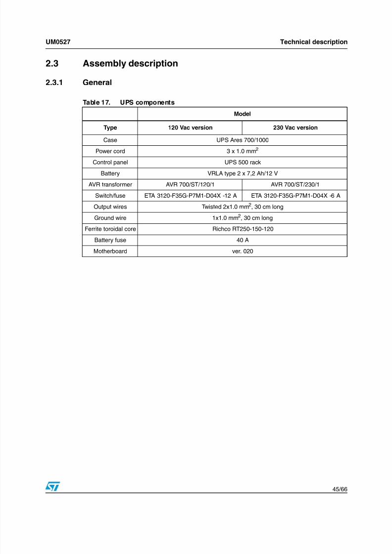
Table 17. UPS components
Model
Type 120 Vac version 230 Vac version
Case UPS Ares 700/1000
Power cord 3 x 1.0 mm2
Control panel UPS 500 rack
Battery VRLA type 2 x 7,2 Ah/12 V
AVR transformer AVR 700/ST/120/1 AVR 700/ST/230/1
Switch/fuse ETA 3120-F35G-P7M1-D04X -12 A ETA 3120-F35G-P7M1-D04X -6 A
Output wires Twisted 2x1.0 mm2, 30 cm long
Ground wire 1x1.0 mm2, 30 cm long
Ferrite toroidal core Richco RT250-150-120
Battery fuse 40 A
Motherboard ver. 020

7/22/2019 UPSSG3525
http://slidepdf.com/reader/full/upssg3525 46/66
Technical description UM0527
46/66
2.3.2 Electrical
The schematic of the electrical connections is shown in Figure 26 .
Figure 26. Electrical connections
2.3.3 Mechanical
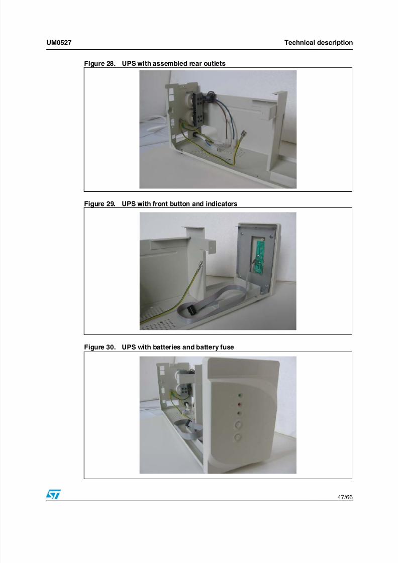
The UPS case with assembled front and power cord.
Figure 27. Mechanical view
7/22/2019 UPSSG3525
http://slidepdf.com/reader/full/upssg3525 47/66
UM0527 Technical description
47/66
Figure 28. UPS with assembled rear outlets
Figure 29. UPS with front button and indicators
Figure 30. UPS with batteries and battery fuse

7/22/2019 UPSSG3525
http://slidepdf.com/reader/full/upssg3525 48/66

7/22/2019 UPSSG3525
http://slidepdf.com/reader/full/upssg3525 49/66
UM0527 Technical description
49/66
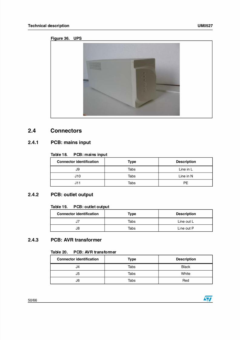
Figure 34. UPS with motherboard
Figure 35. UPS fully assembled
7/22/2019 UPSSG3525
http://slidepdf.com/reader/full/upssg3525 50/66

7/22/2019 UPSSG3525
http://slidepdf.com/reader/full/upssg3525 51/66

7/22/2019 UPSSG3525
http://slidepdf.com/reader/full/upssg3525 52/66
Technical description UM0527
52/66
2.5 Signalization description
2.5.1 Indicators
2.5.2 Sound alarms
2.6 Bill of material
2.6.1 Bill of material for 120 Vac version
Table 25. Indicators
Green LED
(mains)
Yellow LED
(battery)
Red LED
(failure/overload)
Mains mode Solid on Off Off
Battery mode OffSolid on
Flash On (BATLOW)Off
Buck/boost mode Flash on Off Off
Battery charging Solid on Flash on Off
Overload (mains) Solid on Off Flash on
Overload ( battery) Off Solid On Flash on
Self test Solid on Solid on Off
Fault ( mains) Solid on Off Solid on
Fault (battery) Off Solid on Solid on
Standby mode Off OffFlash on
(one per 2 sec.)
Table 26. Sound alarms
State Beeper alarm sequence
Inverter mode 1 beep with 1 s. interval by 15 s. and after this 1 beep with 15 s. interval
Overload 1 beep with 0.3 s. interval
BATLOW continuous signal
State Beeper alarm sequence
Inverter mode 1 beep with 1 s. interval by 15 s. and after this 1 beep with 15 s. interval
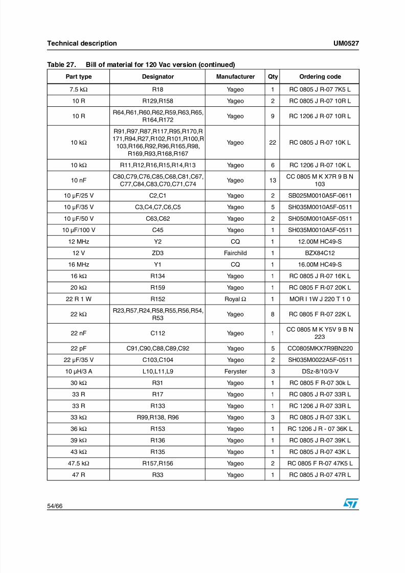
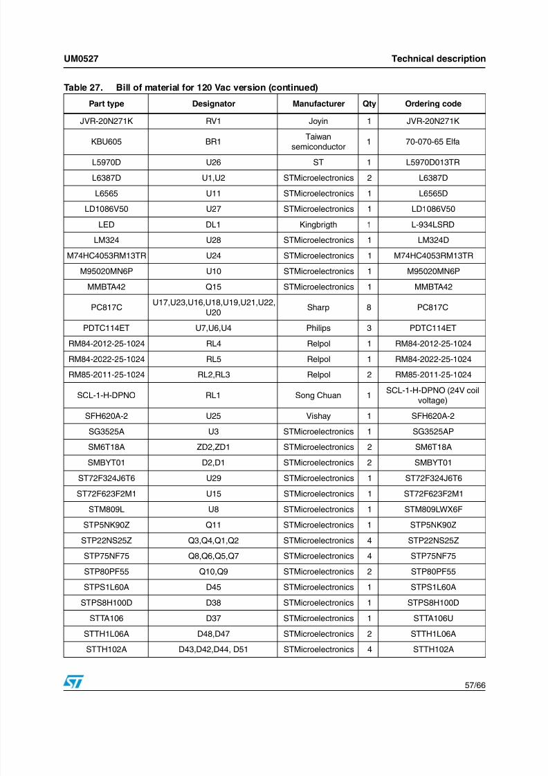
Table 27. Bill of material for 120 Vac version
Part type Designator Manufacturer Qty Ordering code
0.68 R 2 W R137 Royal Ω 1 MOR I 2W J 68K T 1 0
0 R R28 Yageo 1 RC 0805 J R-07 0R L

7/22/2019 UPSSG3525
http://slidepdf.com/reader/full/upssg3525 53/66
7/22/2019 UPSSG3525
http://slidepdf.com/reader/full/upssg3525 54/66
Technical description UM0527
54/66
7.5 kΩ R18 Yageo 1 RC 0805 J R-07 7K5 L
10 R R129,R158 Yageo 2 RC 0805 J R-07 10R L
10 RR64,R61,R60,R62,R59,R63,R65,
R164,R172Yageo 9 RC 1206 J R-07 10R L
10 kΩ
R91,R97,R87,R117,R95,R170,R
171,R94,R27,R102,R101,R100,R
103,R166,R92,R96,R165,R98,
R169,R93,R168,R167
Yageo 22 RC 0805 J R-07 10K L
10 kΩ R11,R12,R16,R15,R14,R13 Yageo 6 RC 1206 J R-07 10K L
10 nFC80,C79,C76,C85,C68,C81,C67,
C77,C84,C83,C70,C71,C74Yageo 13
CC 0805 M K X7R 9 B N
103
10 µF/25 V C2,C1 Yageo 2 SB025M0010A5F-0611
10 µF/35 V C3,C4,C7,C6,C5 Yageo 5 SH035M0010A5F-0511
10 µF/50 V C63,C62 Yageo 2 SH050M0010A5F-0511
10 µF/100 V C45 Yageo 1 SH035M0010A5F-0511
12 MHz Y2 CQ 1 12.00M HC49-S
12 V ZD3 Fairchild 1 BZX84C12
16 MHz Y1 CQ 1 16.00M HC49-S
16 kΩ R134 Yageo 1 RC 0805 J R-07 16K L
20 kΩ R159 Yageo 1 RC 0805 F R-07 20K L
22 R 1 W R152 RoyalΩ
1 MOR I 1W J 220 T 1 0
22 kΩR23,R57,R24,R58,R55,R56,R54,
R53Yageo 8 RC 0805 F R-07 22K L
22 nF C112 Yageo 1CC 0805 M K Y5V 9 B N
223
22 pF C91,C90,C88,C89,C92 Yageo 5 CC0805MKX7R9BN220
22 µF/35 V C103,C104 Yageo 2 SH035M0022A5F-0511
10 µH/3 A L10,L11,L9 Feryster 3 DSz-8/10/3-V
30 kΩ R31 Yageo 1 RC 0805 F R-07 30k L
33 R R17 Yageo 1 RC 0805 J R-07 33R L
33 R R133 Yageo 1 RC 1206 J R-07 33R L
33 kΩ R99,R138, R96 Yageo 3 RC 0805 J R-07 33K L
36 kΩ R153 Yageo 1 RC 1206 J R - 07 36K L
39 kΩ R136 Yageo 1 RC 0805 J R-07 39K L
43 kΩ R135 Yageo 1 RC 0805 J R-07 43K L
47.5 kΩ R157,R156 Yageo 2 RC 0805 F R-07 47K5 L
47 R R33 Yageo 1 RC 0805 J R-07 47R L
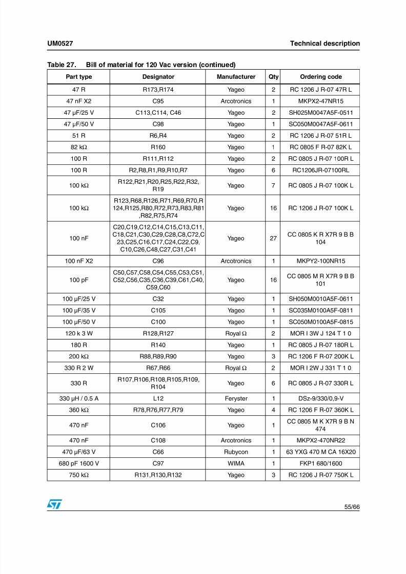
Table 27. Bill of material for 120 Vac version (continued)
Part type Designator Manufacturer Qty Ordering code
7/22/2019 UPSSG3525
http://slidepdf.com/reader/full/upssg3525 55/66
UM0527 Technical description
55/66
47 R R173,R174 Yageo 2 RC 1206 J R-07 47R L
47 nF X2 C95 Arcotronics 1 MKPX2-47NR15
47 µF/25 V C113,C114, C46 Yageo 2 SH025M0047A5F-0511
47 µF/50 V C98 Yageo 1 SC050M0047A5F-0611
51 R R6,R4 Yageo 2 RC 1206 J R-07 51R L
82 kΩ R160 Yageo 1 RC 0805 F R-07 82K L
100 R R111,R112 Yageo 2 RC 0805 J R-07 100R L
100 R R2,R8,R1,R9,R10,R7 Yageo 6 RC1206JR-07100RL
100 kΩR122,R21,R20,R25,R22,R32,
R19Yageo 7 RC 0805 J R-07 100K L
100 kΩR123,R68,R126,R71,R69,R70,R124,R125,R80,R72,R73,R83,R81
,R82,R75,R74
Yageo 16 RC 1206 J R-07 100K L
100 nF
C20,C19,C12,C14,C15,C13,C11,
C18,C21,C30,C29,C28,C8,C72,C
23,C25,C16,C17,C24,C22,C9,
C10,C26,C48,C27,C31,C41
Yageo 27CC 0805 K R X7R 9 B B
104
100 nF X2 C96 Arcotronics 1 MKPY2-100NR15
100 pF
C50,C57,C58,C54,C55,C53,C51,
C52,C56,C35,C36,C39,C61,C40,
C59,C60
Yageo 16CC 0805 M R X7R 9 B B
101
100 µF/25 V C32 Yageo 1 SH050M0010A5F-0611100 µF/35 V C105 Yageo 1 SC035M0100A5F-0811
100 µF/50 V C100 Yageo 1 SC050M0100A5F-0815
120 k 3 W R128,R127 Royal Ω 2 MOR I 3W J 124 T 1 0
180 R R140 Yageo 1 RC 0805 J R-07 180R L
200 kΩ R88,R89,R90 Yageo 3 RC 1206 F R-07 200K L
330 R 2 W R67,R66 Royal Ω 2 MOR I 2W J 331 T 1 0
330 RR107,R106,R108,R105,R109,
R104Yageo 6 RC 0805 J R-07 330R L
330 µH / 0.5 A L12 Feryster 1 DSz-9/330/0,9-V
360 kΩ R78,R76,R77,R79 Yageo 4 RC 1206 F R-07 360K L
470 nF C106 Yageo 1CC 0805 M K X7R 9 B N
474
470 nF C108 Arcotronics 1 MKPX2-470NR22
470 µF/63 V C66 Rubycon 1 63 YXG 470 M CA 16X20
680 pF 1600 V C97 WIMA 1 FKP1 680/1600
750 kΩ R131,R130,R132 Yageo 3 RC 1206 J R-07 750K L
Table 27. Bill of material for 120 Vac version (continued)
Part type Designator Manufacturer Qty Ordering code

7/22/2019 UPSSG3525
http://slidepdf.com/reader/full/upssg3525 56/66
7/22/2019 UPSSG3525
http://slidepdf.com/reader/full/upssg3525 57/66
7/22/2019 UPSSG3525
http://slidepdf.com/reader/full/upssg3525 58/66
Technical description UM0527
58/66
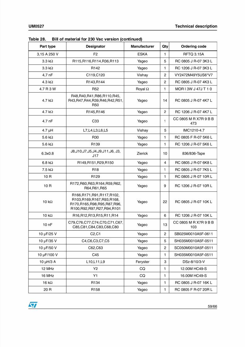
2.6.2 Bill of material for 230 Vac version
STTH302S D30,D29 STMicroelectronics 2 STTH302S
STTH803D D28,D25,D26,D27 STMicroelectronics 4 STTH803D
TI50/30v01 T1 Sigma 1 TI50/30v01
TI700/24/2v01 TI1 Sigma 1 TI700/24/2v01
TL431CD U12 Fairchild 1 TL431CD
TS555CDT U14 STMicroelectronics 1 TS555CDT
TYN608 TH1 STMicroelectronics 1 TYN608RG
ULN2003D U9 STMicroelectronics 1 ULN2003D
USB6B1 U13 STMicroelectronics 1 USB6B1RL
USB-B J13 JST 1 UBB-4R-D10T-1
Table 27. Bill of material for 120 Vac version (continued)
Part type Designator Manufacturer Qty Ordering code
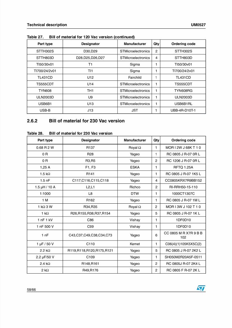
Table 28. Bill of material for 230 Vac version
Part type Designator Manufacturer Qty Ordering code
0.68 R 2 W R137 Royal Ω 1 MOR I 2W J 68K T 1 0
0 R R28 Yageo 1 RC 0805 J R-07 0R L
0 R R3,R5 Yageo 2 RC 1206 J R-07 0R L
1,25 A F1, F3 ESKA 1 RFTQ 1.25A
1.5 kΩ R141 Yageo 1 RC 0805 J R-07 1K5 L
1.5 nF C117,C116,C115,C118 Yageo 4 CC0805KRX7R9BB152
1.5 µH / 10 A L2,L1 Richco 2 RI-RRH50-15-110
1:1000 L8 DTW 1 1000CT1307C
1 M R162 Yageo 1 RC 0805 J R-07 1M L
1 kΩ 3 W R34,R35 Royal Ω 2 MOR I 3W J 102 T 1 0
1 kΩ R26,R155,R38,R37,R154 Yageo 5 RC 0805 J R-07 1K L
1 nF 1 kV C86 Vishay 1 1DF0D10
1 nF 500 V C99 Vishay 1 1DF0D10
1 nF C43,C37,C49,C38,C34,C73 Yageo 6CC 0805 M R X7R 9 B B
102
1 µF / 50 V C110 Kemet 1 C06(4)(1)105K5X5C(2)
2.2 kΩ R119,R118,R120,R175,R121 Yageo 5 RC 0805 J R-07 2K2 L
2.2 µF/50 V C109 Yageo 1 SH050M2R20A5F-0511
2.4 kΩ R148,R161 Yageo 2 RC 0805J R-07 2K4 L
2 kΩ R49,R176 Yageo 2 RC 0805 F R-07 2K L
7/22/2019 UPSSG3525
http://slidepdf.com/reader/full/upssg3525 59/66
UM0527 Technical description
59/66
3,15 A 250 V F2 ESKA 1 RFTQ 3.15A
3.3 kΩ R115,R116,R114,R36,R113 Yageo 5 RC 0805 J R-07 3K3 L
3.3 kΩ R142 Yageo 1 RC 1206 J R-07 3K3 L
4,7 nF C119,C120 Vishay 2 VY2472M49Y5US6*V7
4.3 kΩ R143,R144 Yageo 2 RC 0805 J R-07 4K3 L
4.7 R 3 W R52 Royal Ω 1 MOR I 3W J 47J T 1 0
4.7 kΩ
R48,R40,R41,R86,R110,R45,
R43,R47,R44,R39,R46,R42,R51,
R50
Yageo 14 RC 0805 J R-07 4K7 L
4.7 kΩ R145,R146 Yageo 2 RC 1206 J R-07 4K7 L
4.7 nF C33 Yageo 1CC 0805 M R X7R 9 B B
473
4.7 µH L7,L4,L3,L6,L5 Vishay 5 IMC1210-4.7
5.6 kΩ R30 Yageo 1 RC 0805 F R-07 5K6 L
5.6 kΩ R139 Yageo 1 RC 1206 J R-07 5K6 L
6.3x0.8J8,J10,J7,J5,J4,J9,J11,J6, J3,
J17Zierick 10 836/836-Tape
6.8 kΩ R149,R151,R29,R150 Yageo 4 RC 0805 J R-07 6K8 L
7.5 kΩ R18 Yageo 1 RC 0805 J R-07 7K5 L
10 R R129 Yageo 1 RC 0805 J R-07 10R L
10 RR172,R60,R63,R164,R59,R62,
R64,R61,R65Yageo 9 RC 1206 J R-07 10R L
10 kΩ
R166,R171,R91,R117,R102,
R103,R169,R167,R93,R168,
R170,R165,R98,R95,R87,R96,
R100,R92,R97,R27,R94,R101
Yageo 22 RC 0805 J R-07 10K L
10 kΩ R16,R12,R13,R15,R11,R14 Yageo 6 RC 1206 J R-07 10K L
10 nFC79,C76,C77,C74,C70,C71,C67,
C85,C81,C84,C83,C68,C80Yageo 13
CC 0805 M R X7R 9 B B
103
10 µF/25 V C2,C1 Yageo 2 SB025M0010A5F-0611
10 µF/35 V C4,C6,C3,C7,C5 Yageo 5 SH035M0010A5F-0511
10 µF/50 V C62,C63 Yageo 2 SC050M0010A5F-0511
10 µF/100 V C45 Yageo 1 SH035M0010A5F-0511
10 µH/3 A L10,L11,L9 Feryster 3 DSz-8/10/3-V
12 MHz Y2 CQ 1 12.00M HC49-S
16 MHz Y1 CQ 1 16.00M HC49-S
16 kΩ R134 Yageo 1 RC 0805 J R-07 16K L
20 R R158 Yageo 1 RC 0805 F R-07 20R L
Table 28. Bill of material for 230 Vac version (continued)
Part type Designator Manufacturer Qty Ordering code

7/22/2019 UPSSG3525
http://slidepdf.com/reader/full/upssg3525 60/66
Technical description UM0527
60/66
20 kΩ R159 Yageo 1 RC 0805 F R-07 20K L
22 R 1 W R152 Royal Ω 1 MOR I 1W J 220 T 1 0
22 kΩR24,R55,R53,R57,R56,R58,R54,
R23Yageo 8 RC 0805 F R-07 22K L
22 nF C112 Yageo 1CC 0805 M K Y5V 9 B N
223
22 pF C90,C92,C91,C89,C88 Yageo 5 CC0805MKX7R9BN220
22 µF/35 V C104,C103 Yageo 2 SH035M0022A5F-0511
33 R R17 Yageo 1 RC 0805 J R-07 33R L
33 R R133 Yageo 1 RC 1206 J R-07 33R L
33 kΩ R138,R99, R96 Yageo 3 RC 0805 J R-07 33K L
36 kΩ R153,R31 Yageo 2 RC 1206 J R - 07 36K L
39 kΩ R136 Yageo 1 RC 0805 J R-07 39K L
43 kΩ R135 Yageo 1 RC 0805 J R-07 43K L
47.5 kΩ R156,R157 Yageo 2 RC 0805 F R-07 47K5 L
47 R R33 Yageo 1 RC 0805 J R-07 47R L
47 R R173,R174 Yageo 2 RC 1206 J R-07 47R L
47 nF X2 C95 Arcotronics 1 MKPX2-47NR15
47 µF/25 V C114,C113, C46 Yageo 3 SH025M0047A5F-0511
47 µF/50 V C98 Yageo 1 SC050M0047A5F-0611
51 R R4,R6 Yageo 2 RC 1206 J R-07 51R L
82 kΩ R160 Yageo 1 RC 0805 F R-07 82K L
100 R R112,R111 Yageo 2 RC 0805 J R-07 100R L
100 R R7,R1,R2,R8,R9,R10 Yageo 6 RC 1206 J R-07 100R L
100 kΩ R20,R25,R21,R122,R22,R19 Yageo 6 RC 0805 J R-07 100K L
100 kΩ R123,R125,R126,R124 Yageo 4 RC 1206 J R-07 100K L
100 nF
C26,C18,C30,C29,C48,C21,C25,
C28,C27,C24,C22,C23,C20,C11,
C12,C15,C16,C13,C19,C17,C72,
C14,C31,C9,C10,C8, C41
Yageo 27CC 0805 M K X7R 9 B N
104
100 nF X2 C96 Arcotronics 1 MKPY2-100NR15
100 pF
C40,C52,C61,C35,C51,C59,C39,
C60,C55,C57,C50,C56,C54,C36,
C58,C53
Yageo 16CC 0805 M K X7R 9 B N
101
100 µF/25 V C32 Yageo 1 SH050M0010A5F-0611
100 µF/35 V C105 Yageo 1 SC035M0100A5F-0811
100 µF/50 V C100 Yageo 1 SC050M0100A5F-0815
Table 28. Bill of material for 230 Vac version (continued)
Part type Designator Manufacturer Qty Ordering code

7/22/2019 UPSSG3525
http://slidepdf.com/reader/full/upssg3525 61/66
UM0527 Technical description
61/66
120 kΩ 3 W R128,R127 Royal Ω 2 MOR I 3W J 124 T 1 0
180 R R140 Yageo 1 RC 0805 J R-07 180R L
200 kΩR82,R83,R89,R80,R90,R81,R88,
R70,R72,R68,R69,R73,R71,R75,
R74
Yageo 15 RC 1206 F R-07 200K L
330 R 2 W R66,R67 Royal Ω 2 MOR I 2W J 331 T 1 0
330 RR108,R104,R106,R105,R109,R1
07Yageo 6 RC 0805 J R-07 330R L
330 nF C87 EVOX Rifa 1 PHE426MD6330J
330 µH / 0.9 A L12 Feryster 1 DSz-9/330/0,9-V
390 kΩ R32 Yageo 1 RC 0805 F R-07 390K L
470 nF C106 Yageo 1CC 0805 M K X7R 9 B N
474
470 nF C108 Arcotronics 1 MKPX2-470NR22
470 µF/63 V C66 Rubycon 1 63 YXG 470 M CA 16X20
680 pF 1600 V C97 WIMA 1 FKP1 680/1600
750 kΩR78,R76,R79,R77,R130,R131,
R132Yageo 7 RC 1206 F R-07 750K L
820 R R147 Yageo 1 RC 0805 J R-07 820R L
1000 µF/50 V C101,C102 Rubycon 2 50 YXG 1000 M CA 16X25
3300 µF/35 V C64,C65 Yageo 2 SC035M3300A5F-1836
BAS16
D15,D7,D16,D6,D4,D17,D11,D18
,D23,D24,D20,D14,D13,D10,D19
,D5,D22,D9,D12,D3,D8,D21
Fairchild 22 BAS16
BAT54 D46 Vishay 1 BAT54-GS18
BAT54A D41 Vishay 1 BAT54A-GS18
BAT54C D39 Vishay 1 BAT54C-GS18
BAT54S D40 Vishay 1 BAT54S-GS18
BC846B Q13Infineon
technologies1 BC846B
BC857B Q12,Q14 Fairchild 2 BC857B
BDX53C Q16 STMicroelectronics 1 BDX53C
BPT-14 B1Bestar electronics
industry1 BPT-14
B600C1500 BR2 DC Components 1 B600C1500
BZV55C10 D32,D31
Central
semiconductor ,
microsemi
2 BZV55C10
Table 28. Bill of material for 230 Vac version (continued)
Part type Designator Manufacturer Qty Ordering code

7/22/2019 UPSSG3525
http://slidepdf.com/reader/full/upssg3525 62/66

7/22/2019 UPSSG3525
http://slidepdf.com/reader/full/upssg3525 63/66
UM0527 Technical description
63/66
SCL-1-H-DPNO RL1 Song Chuan 1 SCL-1-H-DPNO 24V
SFH620A-2 U25 Vishay 1 SFH620A-2
SG3525A U3 STMicroelectronics 1 SG3525AP
SM6T18A ZD1,ZD2 STMicroelectronics 2 SM6T18A
SMBYT01 D2,D1 STMicroelectronics 2 SMBYT01
ST72F324J6T6 U29 STMicroelectronics 1 ST72F324J6T6
ST72F623F2M1 U15 STMicroelectronics 1 ST72F623F2M1
STM809L U8 STMicroelectronics 1 STM809LWX6F
STP5NK90Z Q11 STMicroelectronics 1 STP5NK90Z
STP12NM50 Q1,Q2,Q4,Q3 STMicroelectronics 4 STP12NM50
STP75NF75 Q6,Q5,Q8,Q7 STMicroelectronics 4 STP75NF75
STP80PF55 Q10,Q9 STMicroelectronics 2 STP80PF55
STPS1L60A D45 STMicroelectronics 1 STPS1L60A
STPS8H100D D38 STMicroelectronics 1 STPS8H100D
STTA106 D37 STMicroelectronics 1 STTA106U
STTH1L06A D48,D47 STMicroelectronics 2 STTH1L06A
STTH8R06D D27,D26,D25,D28 STMicroelectronics 4 STTH8R06D
STTH102A D43,D42,D44, D51 STMicroelectronics 4 STTH102A
STTH302S D29,D30 STMicroelectronics 2 STTH302S
TI50/30v01 T1 Sigma 1 TI50/30v01
TI700/24/1v01 TI1 Sigma 1 TI700/24/1/v01
TL431CD U12 Fairchild 1 TL431CD
TS555CDT U14 STMicroelectronics 1 TS555CDT
TYN608 TH1 STMicroelectronics 1 TYN608RG
ULN2003D U9 STMicroelectronics 1 ULN2003D
USB6B1 U13 STMicroelectronics 1 USB6B1RL
USB-B J13 JST 1 UBB-4R-D10T-1
Table 28. Bill of material for 230 Vac version (continued)
Part type Designator Manufacturer Qty Ordering code
7/22/2019 UPSSG3525
http://slidepdf.com/reader/full/upssg3525 64/66
7/22/2019 UPSSG3525
http://slidepdf.com/reader/full/upssg3525 65/66
UM0527 Revision history
65/66
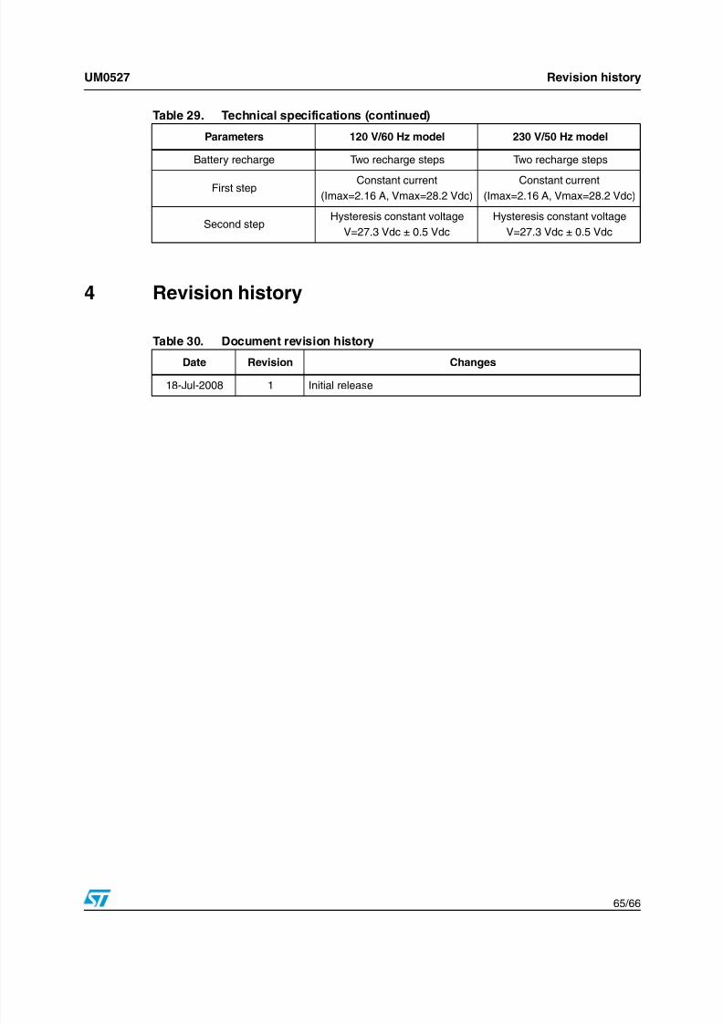
4 Revision history
Battery recharge Two recharge steps Two recharge steps
First step Constant current(Imax=2.16 A, Vmax=28.2 Vdc)
Constant current(Imax=2.16 A, Vmax=28.2 Vdc)
Second stepHysteresis constant voltage
V=27.3 Vdc ± 0.5 Vdc
Hysteresis constant voltage
V=27.3 Vdc ± 0.5 Vdc
Table 29. Technical specifications (continued)
Parameters 120 V/60 Hz model 230 V/50 Hz model
Table 30. Document revision history
Date Revision Changes
18-Jul-2008 1 Initial release

7/22/2019 UPSSG3525
http://slidepdf.com/reader/full/upssg3525 66/66
UM0527
Please Read Carefully:
Information in this document is provided solely in connection with ST products. STMicroelectronics NV and its subsidiaries (“ST”) reserve the
right to make changes, corrections, modifications or improvements, to this document, and the products and services described herein at anytime, without notice.
All ST products are sold pursuant to ST’s terms and conditions of sale.
Purchasers are solely responsible for the choice, selection and use of the ST products and services described herein, and ST assumes no
liability whatsoever relating to the choice, selection or use of the ST products and services described herein.
No license, express or implied, by estoppel or otherwise, to any intellectual property rights is granted under this document. If any part of this
document refers to any third party products or services it shall not be deemed a license grant by ST for the use of such third party products
or services, or any intellectual property contained therein or considered as a warranty covering the use in any manner whatsoever of such
third party products or services or any intellectual property contained therein.
UNLESS OTHERWISE SET FORTH IN ST’S TERMS AND CONDITIONS OF SALE ST DISCLAIMS ANY EXPRESS OR IMPLIED
WARRANTY WITH RESPECT TO THE USE AND/OR SALE OF ST PRODUCTS INCLUDING WITHOUT LIMITATION IMPLIED
WARRANTIES OF MERCHANTABILITY, FITNESS FOR A PARTICULAR PURPOSE (AND THEIR EQUIVALENTS UNDER THE LAWS
OF ANY JURISDICTION), OR INFRINGEMENT OF ANY PATENT, COPYRIGHT OR OTHER INTELLECTUAL PROPERTY RIGHT.
UNLESS EXPRESSLY APPROVED IN WRITING BY AN AUTHORIZED ST REPRESENTATIVE, ST PRODUCTS ARE NOT
RECOMMENDED, AUTHORIZED OR WARRANTED FOR USE IN MILITARY, AIR CRAFT, SPACE, LIFE SAVING, OR LIFE SUSTAINING
APPLICATIONS, NOR IN PRODUCTS OR SYSTEMS WHERE FAILURE OR MALFUNCTION MAY RESULT IN PERSONAL INJURY,
DEATH, OR SEVERE PROPERTY OR ENVIRONMENTAL DAMAGE. ST PRODUCTS WHICH ARE NOT SPECIFIED AS "AUTOMOTIVE
GRADE" MAY ONLY BE USED IN AUTOMOTIVE APPLICATIONS AT USER’S OWN RISK.
Resale of ST products with provisions different from the statements and/or technical features set forth in this document shall immediately void
any warranty granted by ST for the ST product or service described herein and shall not create or extend in any manner whatsoever, any
liability of ST.
ST and the ST logo are trademarks or registered trademarks of ST in various countries.
Information in this document supersedes and replaces all information previously supplied.
The ST logo is a registered trademark of STMicroelectronics. All other names are the property of their respective owners.
© 2008 STMicroelectronics - All rights reserved
STMicroelectronics group of companies