UOTFT: Universal Organic TFT Model for Circuit Design International Conference on Organic Electronics 2009 S. Mijalković, D. Green, A. Nejim Silvaco Europe, St Ives, Cambridgeshire, UK A. Rankov, E. Smith, T. Kugler, C. Newsome, J. Halls Cambridge Display Technologies, Godmanchester, UK

Welcome message from author
This document is posted to help you gain knowledge. Please leave a comment to let me know what you think about it! Share it to your friends and learn new things together.
Transcript

UOTFT: Universal Organic TFT Model for Circuit Design
International Conference on Organic Electronics 2009 S. Mijalković, D. Green, A. Nejim
Silvaco Europe, St Ives, Cambridgeshire, UK A. Rankov, E. Smith, T. Kugler, C. Newsome, J. Halls
Cambridge Display Technologies, Godmanchester, UK

UOTFT: Universal Organic TFT Model for Circuit Design
• Introduction • Organic electronics as a challenge for EDA • TSB Project PMOS
• UOTFT Model Description • Objectives and close relatives • Model features • Physics behind the model • UCCM for OTFTs • Intrinsic drain-source current
• Model verification • DC characteristic and temperature scaling for different OSC materials and device
architectures
Overview
International Conference on Organic Electronics 2009
2

UOTFT: Universal Organic TFT Model for Circuit Design
• Inorganic semiconductor industry relies extensively on EDA software to support the iterative cycles of process, device and circuit technology improvements
• To further develop organic electronics industry, equivalent design tools are needed
• EDA tools essentially depend on numerical and compact device models which are, in case of OSCs, not yet matured and quite sparsely implemented in commercial EDA tools
• Cambridge Display Technology (CDT) and Silvaco Europe have joined forces in a TSB funded project entitled PMOS to enhance EDA tools for use in the organic electronics
Organic Electronics: Challenge for Electronic Design Automation (EDA)
3
International Conference on Organic Electronics 2009

UOTFT: Universal Organic TFT Model for Circuit Design
Project partners • Cambridge Display Technology (CDT)
• Expert in polymer light emitting diode (PLED) technologies • Leader in development of solution processable (printable) organic. semiconductors for display
fabrication • Expertise in development of PLED materials and deposition processes
• Silvaco • Leading provider of TCAD and EDA software for IC design • Provides established products for TCAD process and device simulation, spice modeling and parameter
extraction, circuit simulation, custom IC design and verification
Project activities • Design of OTFT devices using physical TCAD modeling • OTFT spice model development • Measurements and modeling of device reliability and aging effects
• The focus is on display device (OLED) drivers as these will be the first large scale organic semiconductor products
UK Technology Strategy Board (TSB) Project: Physical Modelling of Organic Semiconductors (PMOS)
4
International Conference on Organic Electronics 2009

UOTFT: Universal Organic TFT Model for Circuit Design
Objectives: • Physical (charge or surface potential based)
compact model dedicated to OTFTs • Small number of ease to extract parameters • Compatible to simple Vth-based OTFT models in
over-threshold region • Suitable for different OSC materials and OTFT
device architectures
UOTFT Model: Objectives and Close Relatives
5
International Conference on Organic Electronics 2009
1
10
100
1000
1970 1980 1990 2000 2010
Level 1 Level 2
Level 3
Bsim
MM9
Bsim2 Bsim4
PSP
UOTFT
Year
Num
ber o
f P
aram
eter
s
Universal FET Modelling Approach Prof. Michael Shur et al. Prof. Benjamin Iñiguez et al.
MOSA1, NPMOSA1-3, etc. Silicon Mosfets, Hfet, Mesfet AIM-Spice
RPI Thin-Film Transistor Models Amorphous and Polysilicon TFTs AIM-Spice, Spectre, Hspice, SmartSpice
UOTFT Organic TFTs SmartSpice
UOTFT: Universal Organic TFT Model for Circuit Design
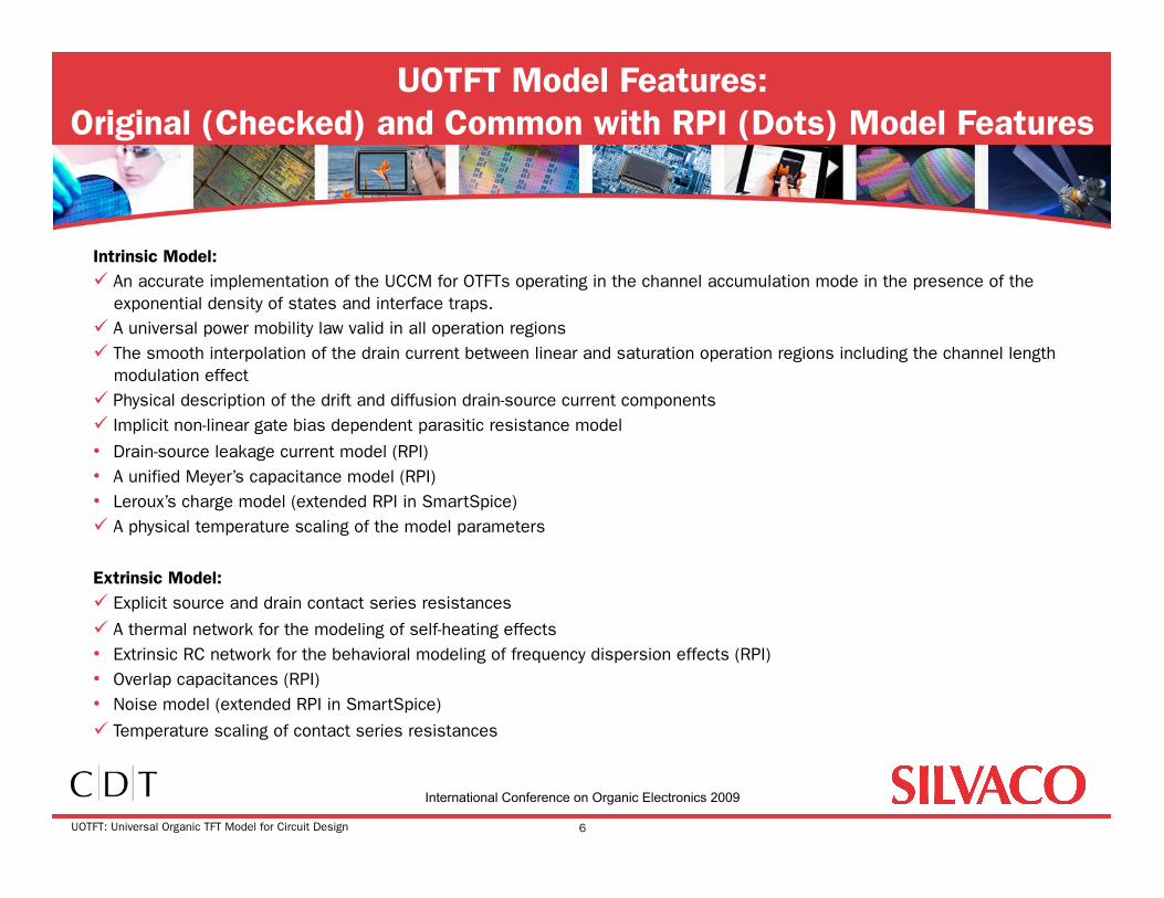
Intrinsic Model: An accurate implementation of the UCCM for OTFTs operating in the channel accumulation mode in the presence of the
exponential density of states and interface traps. A universal power mobility law valid in all operation regions The smooth interpolation of the drain current between linear and saturation operation regions including the channel length
modulation effect Physical description of the drift and diffusion drain-source current components Implicit non-linear gate bias dependent parasitic resistance model
• Drain-source leakage current model (RPI) • A unified Meyer’s capacitance model (RPI) • Leroux’s charge model (extended RPI in SmartSpice) A physical temperature scaling of the model parameters
Extrinsic Model: Explicit source and drain contact series resistances
A thermal network for the modeling of self-heating effects • Extrinsic RC network for the behavioral modeling of frequency dispersion effects (RPI) • Overlap capacitances (RPI) • Noise model (extended RPI in SmartSpice)
Temperature scaling of contact series resistances
UOTFT Model Features: Original (Checked) and Common with RPI (Dots) Model Features
6
International Conference on Organic Electronics 2009

UOTFT: Universal Organic TFT Model for Circuit Design
Physics Behind UOTFT: Carrier Concentration and OSC Conductivity
7
International Conference on Organic Electronics 2009
Vissenberg and Ma-ers, Phys. Rev. B, 1998.
Exponential DOS distribution
Percolation Theory

UOTFT: Universal Organic TFT Model for Circuit Design
UOTFT Electrostatics: Unified Charge Control Model (UCCM) for OTFTs
8
International Conference on Organic Electronics 2009
UCCM
Surface Potential Description

UOTFT: Universal Organic TFT Model for Circuit Design
UOTFT Electrostatics: Accurate Implementation of UCCM
9
International Conference on Organic Electronics 2009
UCCM Exact SP Model

UOTFT: Universal Organic TFT Model for Circuit Design
UOTFT Effective Conductivity (Mobility) Model: Applied Percolation Theory
10
International Conference on Organic Electronics 2009
Exact
Model

UOTFT: Universal Organic TFT Model for Circuit Design
UOTFT DC Model: Intrinsic Drain-Source Current
11
International Conference on Organic Electronics 2009
drift diffusion

UOTFT: Universal Organic TFT Model for Circuit Design
Parameter Extraction in Utmost IV
12
International Conference on Organic Electronics 2009

UOTFT: Universal Organic TFT Model for Circuit Design
Model Verification: Bottom Gate Bottom Contact (BGBC) OTFT Devices (3rd party OSC material: material A)
13
International Conference on Organic Electronics 2009
Comparison between simulated (lines) and measured (circles) transfer characteristics of the OTFT in the linear operation region with Vds=-3V (blue line and circles) and saturation operation
region with Vds=-30V (red line and circles)
Comparison between simulated (lines) and measured (circles) output characteristics of the
OTFT for Vg=-10V, -20V, -30V and -40V.

UOTFT: Universal Organic TFT Model for Circuit Design
Model verification: Top Gate Bottom Contact (TGBC) OTFT Devices (3rd party OSC material: material B)
14
International Conference on Organic Electronics 2009
Comparison between simulated (lines) and measured (circles) transfer
(Vds=-30V) and output characteristics of the OTFT with a polymer OSC.

UOTFT: Universal Organic TFT Model for Circuit Design
• Comparison between simulated (lines) and measured (circles) transfer characteristics for two different device architectures and two different materials in the saturation operation region at different temperatures
Model Verification: Temperature Scaling (BGBC and TGBC with different 3rd party OSC materials)
15
International Conference on Organic Electronics 2009
OSC material: A BGBC structure

UOTFT: Universal Organic TFT Model for Circuit Design
• Gate leakage-current model • Poole-Frenkel trap assisted tunneling in the insulator • Source/drain partitioning scheme • Temperature dependence of the model parameter
• Physical drain-source leakage current • Advanced temperature scaling of the leakage current model parameters
• Short channel effects • Improved channel length modulation model
• Effects of the depletion and strong lateral electric field on the drain side • Space-charge limited transport
• Effective channel conductivity for poly-crystalline OSC materials • Effective poly-crystalline mobility
UOTFT Model Features Under Development: The Next Six-Month-Roadmap
16
International Conference on Organic Electronics 2009

UOTFT: Universal Organic TFT Model for Circuit Design
Acknowledgement
17
International Conference on Organic Electronics 2009
We want to thank Prof. Benjamin Iñiguez and his group for valuable recommendations regarding
compact organic TFT modeling.
This work is supported by the UK Technology Strategy Board
through the PMOS project TP/J2519J.
Related Documents