With respect to the information represented in this material, Novatek makes no warranty, expressed or implied, including the warranties of merchantability, fitness for a particular purpose and non-infringement, nor assumes any legal liability or responsibility for the accuracy, completeness, or usefulness of any such information. NT35582 One-chip Driver IC with internal GRAM for 16.77M colors 480RGB x 864 / 800 / 640 LTPS TFT LCD with CPU / RGB / MDDI Interface Version 0.02 2008/12/05

Welcome message from author
This document is posted to help you gain knowledge. Please leave a comment to let me know what you think about it! Share it to your friends and learn new things together.
Transcript
With respect to the information represented in this material, Novatek makes no warranty, expressed or implied, including the warranties of merchantability, fitness for a particular purpose and non-infringement, nor assumes any legal liability or responsibility for the accuracy, completeness, or usefulness of any such information.
NT35582 One-chip Driver IC with internal GRAM for 16.77M colors 480RGB x 864 / 800 / 640 LTPS TFT LCD with CPU / RGB / MDDI Interface
Version 0.02 2008/12/05

Preliminary NT35582
1/21/2009 1 V0.02 With respect to the information represented in this material, Novatek makes no warranty, expressed or implied, including the warranties of merchantability, fitness for a particular purpose and non-infringement, nor assumes any legal liability or responsibility for the accuracy, completeness, or usefulness of any such information.
INDEX REVISION HISTORY ................................................................................................4
1. GENERAL DESCRIPTION ...................................................................................5 1.1 PURPOSE OF THIS DOCUMENT........................................................................................................ 5 1.2 GENERAL DESCRIPTION ................................................................................................................. 5
2. FEATURES...........................................................................................................6
3. BLOCK DIAGRAM ...............................................................................................8
4. PIN DESCRIPTIONS ............................................................................................9 4.1 POWER INPUTS.............................................................................................................................. 9 4.2 80-SYSTEM INTERFACE.................................................................................................................. 9 4.3 SPI INTERFACE............................................................................................................................ 10 4.4 I2C INTERFACE............................................................................................................................ 10 4.5 RGB INTERFACE.......................................................................................................................... 10 4.6 MDDI INTERFACE .........................................................................................................................11 4.7 CABC+LABC CONTROL PINS.......................................................................................................11 4.8 INTERFACE LOGIC PINS ................................................................................................................ 12 4.9 DISPLAY DRIVE ANALOG OUTPUTS ............................................................................................... 14 4.10 DISPLAY DRIVE DIGITAL OUTPUTS ............................................................................................... 14 4.11 POWER SUPPLY ......................................................................................................................... 15 4.12 TEST PINS (TEST AND DUMMY PINS) ........................................................................................... 16
5. FUNCTION DESCRIPTION................................................................................17 5.1 MPU INTERFACE ..................................................................................................................... 17
5.1.1 General Protocol ................................................................................................................ 17 5.1.2 80-System Interface........................................................................................................... 18
5.1.2.1 Write cycle sequence ................................................................................................................ 19 5.1.2.2 Read Cycle Sequence............................................................................................................... 20
5.1.3 Serial Interface................................................................................................................... 21 5.1.3.1 Write Mode................................................................................................................................ 21 5.1.3.2 Read Mode................................................................................................................................ 25
5.1.4 Data Transfer Pause .......................................................................................................... 27 5.1.4.1 Parallel Interface Pause ............................................................................................................ 27 5.1.4.2 Serial Interface Pause ............................................................................................................... 27
5.1.5 Data Transfer Break and Recovery ................................................................................... 28 5.1.6 Display Module Data Transfer Modes................................................................................ 29
5.1.6.1 Method 1 ................................................................................................................................... 29 5.1.6.2 Method 2 ................................................................................................................................... 29
5.2 DISPLAY DATA RAM (DDRAM)................................................................................................. 30 5.2.1 3-wire Serial Interface for DATA RAM write ....................................................................... 31
5.2.1.1 65K Colors (5-6-5 Bits Input)..................................................................................................... 31 5.2.1.2 262K Colors (6-6-6 Bits Input) ................................................................................................... 33 5.2.1.3 16.7M Colors (6-6-6 Bits Input) ................................................................................................. 35
5.2.2 8-Bit Parallel Interface for Data RAM Write ....................................................................... 37 5.2.2.1 65K Colors (5-6-5 Bits Input)..................................................................................................... 37 5.2.2.2 262K Colors (6-6-6 Bits Input) ................................................................................................... 38 5.2.2.3 16.7M Colors (8-8-8 Bits Input) ................................................................................................. 39
5.2.3 16-Bit Parallel Interface for Data RAM Write ..................................................................... 40 5.2.3.1 65K Colors (5-6-5 Bits Input)..................................................................................................... 40 5.2.3.2 262K Colors (6-6-6 Bits Input) ................................................................................................... 41 5.2.3.3 16.7M Colors (8-8-8 Bits Input) ................................................................................................. 42
5.2.4 24-Bit Parallel Interface for Data RAM Write ..................................................................... 43 5.2.4.1 65K Colors (5-6-5 Bits Input)..................................................................................................... 43 5.2.4.2 262K Colors (6-6-6 Bits Input) ................................................................................................... 44

Preliminary NT35582
1/21/2009 2 V0.02 With respect to the information represented in this material, Novatek makes no warranty, expressed or implied, including the warranties of merchantability, fitness for a particular purpose and non-infringement, nor assumes any legal liability or responsibility for the accuracy, completeness, or usefulness of any such information.
5.2.4.3 16.7M Colors (8-8-8 Bits Input) ................................................................................................. 45 5.2.5 Serial Interface for DATA RAM Read................................................................................. 46
5.2.5.1 Read Data for RGB 5-6-5- Bits.................................................................................................. 46 5.2.5.2 Read Data for RGB 6-6-6- Bits.................................................................................................. 49 5.2.5.3 Read Data for RGB 8-8-8- Bits.................................................................................................. 52
5.2.6 8-Bit Parallel Interface for Data RAM Read....................................................................... 55 5.2.7 16-Bit Parallel Interface for Data RAM Read..................................................................... 58 5.2.8 24-Bit Parallel Interface for Data RAM Read..................................................................... 61
5.3 RGB INTERFACE.......................................................................................................................... 64 5.3.1 General Description.......................................................................................................... 64 5.3.2 General Timing Diagram .................................................................................................. 65 5.3.3 RGB Interface Bus Width Set........................................................................................... 66 5.3.4 RGB Interface Mode Set.................................................................................................. 66 5.3.5 RGB Interface Mode 1 & Mode 2 TIMING CHART ........................................................... 67
5.4 I2C INTERFACE............................................................................................................................ 70 5.4.1 Slave Address ................................................................................................................... 71 5.4.2 Register Write Sequence ................................................................................................. 72 5.4.3 RAM Data Write Sequence .............................................................................................. 72
5.4.3.1 16 Bits RAM Data Write Sequence (3A00h + 0x0005)............................................................ 72 5.4.3.2 18 Bits RAM data write Sequence (3A00h + 0x0006)............................................................. 73 5.4.3.3 24 Bits RAM data write Sequence (3A00h + 0x0007)............................................................. 73
5.4.4 Register Read Sequence ................................................................................................. 74 5.4.5 RAM Data Read Sequence.............................................................................................. 74
5.4.5.1 16 Bits RAM data read Sequence (3A00h + 0x0005) ............................................................. 75 5.4.5.2 18 Bits RAM data read Sequence (3A00h + 0x0006) ............................................................. 75 5.4.5.3 24 Bits RAM data read Sequence (3A00h + 0x0007) ............................................................. 76
5.5 FRAME TEARING EFFECT INTERFACE ............................................................................................ 77 5.5.1 Example 1: MPU Write is Faster than Panel Read............................................................ 77 5.5.2 Example 2: MPU Write is Slower than Panel Read........................................................... 78 5.5.2 FTE Output Position Setting ............................................................................................. 80
5.6 DYNAMIC BACKLIGHT CONTROL FUNCTION ................................................................................... 81 5.6.1 PWM Control Architecture ................................................................................................. 84 5.6.2 Content Adaptive Brightness Control (CABC) ................................................................... 90 5.6.3 Ambient Light Sensor & Automatic Brightness Control (LABC) ........................................ 91
5.6.3.1 AD Converter............................................................................................................................. 92 5.6.3.2 50 / 60Hz Flicker Removal. ....................................................................................................... 92 5.6.3.3 Light Guide Compensation. ....................................................................................................... 93 5.6.3.4 Median Filter.............................................................................................................................. 94 5.6.3.5 Hysteresis.................................................................................................................................. 95
5.7 MOBILE DISPLAY DIGITAL INTERFACE (MDDI)................................................................................ 98 5.7.1 MDDI Link Protocol by the NT35582 ................................................................................. 99 5.7.2 MDDI Link Packet Descriptions by the NT35582 ............................................................ 100 5.7.3 Writing Video Data to Memory Sequence ....................................................................... 109 5.7.4 Writing Register Sequence .............................................................................................. 109 5.7.5 Reading Video Data from Memory Sequence ..................................................................110 5.7.6 Reading Register Sequence.............................................................................................110 5.7.7 Hibernation Setting ...........................................................................................................111 5.7.8 Deep Standby Mode Setting by MDDI..............................................................................112
5.8 HIGH-SPEED RAM WRITE FUNCTION ..........................................................................................114 5.8.1 High-Speed RAM Data Write in Window Address Area ...................................................115
5.9 WINDOW ADDRESS FUNCTION.....................................................................................................116 5.10 REDUCED POWER CONSUMPTION DRIVE SETTINGS ...................................................................117 5.11 ZIGZAG, COLUMN, 1-DOT, 2-DOT INVERSION (VCOM DC DRIVE) ...............................................117 5.12 FRAME FREQUENCY ADJUSTMENT FUNCTION.............................................................................118 5.13 GAMMA CORRECTION FUNCTION .....................................................................................119 5.14 RESET FUNCTION .................................................................................................................... 120 5.15 BASIC OPERATION MODE ......................................................................................................... 122 5.16 POWER SUPPLY SETTING SEQUENCE ....................................................................................... 123

Preliminary NT35582
1/21/2009 3 V0.02 With respect to the information represented in this material, Novatek makes no warranty, expressed or implied, including the warranties of merchantability, fitness for a particular purpose and non-infringement, nor assumes any legal liability or responsibility for the accuracy, completeness, or usefulness of any such information.
5.17 INSTRUCTION SETTING SEQUENCE ........................................................................................... 124 5.17.1 Sleep SET/EXIT Sequences.......................................................................................... 124 5.17.2 Deep Standby Mode SET/EXIT Sequences.................................................................. 125
5.18 NVM WRITE SEQUENCE .......................................................................................................... 126 5.19 INSTRUCTION SETUP F LOW...................................................................................................... 127
5.19.1 Initializing with the Build-in Power Supply Circuit .......................................................... 127 5.19.2 Power Off Sequence...................................................................................................... 128
5.20 POWER BLOCK ........................................................................................................................ 129 5.21 MAXIMUM SERIES RESISTANCE ................................................................................................ 130 5.22 EXTERNAL COMPONENTS CONNECTION .................................................................................... 131
6. COMMAND DESCRIPTIONS ...........................................................................132 6.1 USER COMMAND SET................................................................................................................. 132 6.2 MANUFACTURE COMMAND SET .................................................................................................. 249
7. ELECTRICAL CHARACTERISTICS ................................................................288 7.1 ABSOLUTE MAXIMUM RATINGS........................................................................................... 288 7.2 DC CHARACTERISTICS ........................................................................................................ 289
7.2.1 Basic Characteristics ....................................................................................................... 289 7.2.2 Current Consumption....................................................................................................... 290 7.2.3 MDDI DC Characteristics................................................................................................. 290
7.3 AC CHARACTERISTICS......................................................................................................... 291 7.3.1 80-System Bus Interface Timing Characteristics (24-/16-/8-bit Transfer Mode) ............. 291 7.3.2 80-System Bus Interface Timing Characteristics (24-bit Transfer Mode) ........................ 292 7.3.3 80-System Bus Interface Timing Characteristics (16-bit / 8-bit Transfer Mode).............. 293 7.3.4 Serial Interface Timing Characteristics ............................................................................ 294 7.3.5 MDDI Interface Characteristics........................................................................................ 295 7.3.6 RGB Interface Characteristics ......................................................................................... 296 7.3.7 I2C-Bus Timing Characteristics ....................................................................................... 298 7.3.8 Reset Timing Characteristics........................................................................................... 299 7.3.9 Liquid Crystal Driver Output Characteristics.................................................................... 300 7.3.10 A/D Converter Characteristics ....................................................................................... 301
8. MECHANICAL CHARACTERISTIC ................................................................302 8.1 CHIP INFORMATION .................................................................................................................... 302 8.2 BUMP INFORMATION................................................................................................................... 302
8.2.1 Output Bump Dimension (Source/ Gate /Dummy) .......................................................... 302 8.2.2 Input Bump Dimension................................................................................................... 303 8.2.3 Alignment mark information............................................................................................. 303 8.2.4 Bump Location and Dimension ....................................................................................... 304
8.3 PAD COORDINATE ...................................................................................................................... 305

Preliminary NT35582
1/21/2009 4 V0.02 With respect to the information represented in this material, Novatek makes no warranty, expressed or implied, including the warranties of merchantability, fitness for a particular purpose and non-infringement, nor assumes any legal liability or responsibility for the accuracy, completeness, or usefulness of any such information.
REVISION HISTORY
Version Contents Prepared by
Checked by
Approved By Date
0.00 Preliminary Version 0.0 KUEI SW LUOH DENNIS 2008/07/25
0.01
1. Modify Reg. 3B00h for ICM,DP,EP,HSP,VSP 2. Modify Reg. 3600h for CTB,CRL 3. Delete SET_GAMMA_CURVE: Gamma Set (2600h) command 4. Delete Display Waveform Cycle setting in partial mode (B200h) command 5. Modify 5000h~500Fh COMMAND 6. Modify 6500h~6503h COMMAND 7. Modify 6F00h COMMAND 8. Update reset time. 9. Modify 5300h command 10. Add external components connection 11. Maximum series resistance 12. Add RGB Mode 2 13. Update Parallel Interface for data ram write diagram 14. Add Mechanical Characteristic
KUEI SW LUOH DENNIS 2008/08/15
0.02
1. Modify B100 COMMAND DATA 2. Modify block diagram 3. Modify RGB interface feature 4. Modify LABC Function feature 5. Remove RGB interface command SYNCCTL(3B01h) 6. Add MDDI Interface Description note 7. Modify Figure 73. RGB interface 8. Add CABC_MOV_PWM command 9. Modify 4F00 Deep standby command 10. Modify Power Supply Setting Sequence 11. Modify Deep Standby Mode ENTER/EXIT sequences 12. Modify 5306h command 13. Modify NVM Write Sequence 14. Modify Power Off Sequence 15. Modify booster voltage DC SPEC 16. Remove Vgamma voltage offset mode 17. Modify AVSS pad(63,64,65) to AVSSR 18. Add AVSSR pad name 19. Modify the typo in the specification 20. Update the Section 7.2 DC Characteristics data 21. Update the Section 7.3 AC Characteristics data 22. Add Section 7.3.10 A/D Converter Characteristics
KUEI SW LUOH DENNIS 2008/12/05

Preliminary NT35582
1/21/2009 5 V0.02 With respect to the information represented in this material, Novatek makes no warranty, expressed or implied, including the warranties of merchantability, fitness for a particular purpose and non-infringement, nor assumes any legal liability or responsibility for the accuracy, completeness, or usefulness of any such information.
1. General Description
1.1 Purpose of this Document This document has been created to provide complete reference specifications for the NT35582. IC design engineers should refer to these specifications when designing ICs, test engineers when testing the compliance of manufactured ICs to guarantee their performance, and application engineers when helping customers to make sure they are using this IC properly.
1.2 General Description The NT35582 device is a single-chip solution for LTPS TFT LCD that incorporates gate drivers and is capable of 480RGBx800 (portrait),480RGBx864 (portrait) and 480RGBx640 (portrait), . It includes a 1,244,160-byte internal memory, a timing controller with glass interface level-shifters, a VCOM driver and a glass power supply circuit. The NT35582 supports Mobile Display Serial Interface (MDDI), RGB interface, 8/16/24-bit MPU system interfaces, serial peripheral interfaces (SPI) and I2C interface. The specified window area can be updated selectively, so that moving pictures can be displayed simultaneously independent of the still picture area. The NT35582 is also able to make gamma correction settings separately for RGB dots to allow benign adjustments to panel characteristics, resulting in higher display qualities. The IC possesses internal GRAM that stores 480-RGB x 864-dot 16.7M-color images, as well as internal boosters that generate the LCD driving voltage, breeder resistance and voltage follower circuit for the LCD driver. A deep standby mode is also supported for lower power consumption. The NT35582 also supports CABC and LABC function for the backlight control. It’s able to reduce the total power consumption of display module significantly. This LSI is suitable for small or medium-sized portable mobile solutions requiring long-term driving capabilities, including bi-directional pagers, digital audio players, cellular phones and handheld PDA.

Preliminary NT35582
1/21/2009 6 V0.02 With respect to the information represented in this material, Novatek makes no warranty, expressed or implied, including the warranties of merchantability, fitness for a particular purpose and non-infringement, nor assumes any legal liability or responsibility for the accuracy, completeness, or usefulness of any such information.
2. Features Single-chip WVGA LTPS controller/driver. Display resolutions
480RGB x 864 (1:3 Multiplexer for source driver, Source output from S1 to S480) 480RGB x 800 (1:3 Multiplexer for source driver, Source output from S1 to S480) 480RGB x 640 (1:3 Multiplexer for source driver, Source output from S1 to S480) Display data memory: 1,244,160 bytes.
Display modes Full color: 16.77M-colors Reduced color: 262K-colors Reduced color: 65K-colors Idle mode: 8-colors
Interfaces 8-bit, 16-bit or 24-bit interfaces with 80-series MPU Serial Peripheral Interface (SPI) I2C Interface 16bit, 18-bit, 24-bit RGB interface
1.RGB I/F Polarity of H/V could be set by register. Mobile Display Digital Interface (MDDI 1.0)
1.MDDI I/F Supported Read function. Display features
High-speed RAM write function Window address functions for specifying a rectangular area on the internal RAM to write data Individual gamma correction setting for RGB dots Deep standby function.
On chip DC/DC converter DC VCOM voltage generator Provide 4 times MTP to store VCOM and ID setting Oscillator for display clock generation
Content Adaptive Backlight Control (CABC) Function Histogram analysis & data process Moving picture auto-detect mode.(UI or still picture mode decided by host) Dimming control 2 level PWM control line for the Display Backlight
Light sensor based Automatic Backlight Control (LABC) Function. Provide 16 levels for brightness setting. Could set brightness manually. LABC/CABC could be turned on/off separately.
Panel Inversion Type Support 1dot inversion , 2dot inversion, column inversion, zigzag inversion driving
Supply voltage range Analog supply voltage range VCI to AVSS: 2.5 to 3.3V I/O supply voltage range for VDDI to VSS: 1.65 to 3.3V MDDI supply voltage range for VDDAM to VSS: 2.5 to 3.3V
Preliminary NT35582
1/21/2009 7 V0.02 With respect to the information represented in this material, Novatek makes no warranty, expressed or implied, including the warranties of merchantability, fitness for a particular purpose and non-infringement, nor assumes any legal liability or responsibility for the accuracy, completeness, or usefulness of any such information.
Output voltage level Positive polarity Source output high voltage level: VGMP = 2.92V to 6.288V Positive polarity Source output low voltage level: VGSP= 0.00V to 3.728V Negative polarity Source output high voltage level: VGMN= -2.92V to -6.288V Negative polarity Source output low voltage level: VGSN= 0.00V to -3.728V Positive Power supply for driver circuit range(AVDD): AVDD-VSS = 5.8V to 6.5V Negative Power supply for driver circuit range(AVEE): AVEE-VSS = -5.8V to -6.5V Positive gate driver output voltage level: VGH-VSS = 7.5V to 15.0V Negative gate driver output voltage level: VGL-AVSS = – 15.0V to –7.5V Common electrode output voltage level: VCOM = +2.0 V to -2.0V
Supports an interface to the gate driver incorporated in the LCD panel

Preliminary NT35582
1/21/2009 8 V0.02 With respect to the information represented in this material, Novatek makes no warranty, expressed or implied, including the warranties of merchantability, fitness for a particular purpose and non-infringement, nor assumes any legal liability or responsibility for the accuracy, completeness, or usefulness of any such information.
3. Block Diagram
480 Source Buffer
D/A Converter
Level Shifter
Data Latch
Level ShifterBIAS
Gamma Generator
Display Data RAM480x864x24=1,244,160 bytes
Address Counter
RAM Data Generator MTP
Instruction Control
System Clock Generator
MPU I/F & Data Latch (SPI, 8/16/24-bit Parallel), I2C, RGB and MDDI I/F
Oscillator
VP_MDDIVREF
Gate Output
Generator
VCOM Generator
LDO
C41P/C41N
VREF
IM[3:0], SA
[1:0]
LTPS TFT LCD Panel
D[23:0]
DC
X
VCOM
SOUT1 ~ SOUT15
VGH VGL
SDI
CABCBacklightControl
LED_ONLED_PWM
SDO
CSX
RD
XW
RX/SC
L
RESX
DE
HS
VS PCLK
FTE
MD
DI_STB
_P/NM
DD
I_DA
TA_P/N
FRM
VCI
VDD
IVD
DA
MVSSA
VSS
VG_M
DD
I
NB
WSEL
TB
NVDD
S1~S480
C42P/C42/N
AVDD
VCC
VGHVGL
RL
LABC
A/DALS
Charge Pump(1 & 2)
Charge Pump(3 & 4)
C11P/C11M
VCI
AVDD
VGMP/N, VGSP/N
VREF
VGMP/VGMNC
VSS
MPU, SPI, RGB & MDDI Interface
I2C_SD
AI2C
_SCL
VCL
VGSP/VGSN
C12P/C12M
AVEE
C31P/C31NC32P/C32/N
VCI
AVEE
C13P/C13MC14P/C14M
C21P/C21MC22P/C22MC23P/C23MC24P/C24M
MTP_PW
RG
M[2:0]
PNL
SHU
T
Figure.1 Block Diagram
Preliminary NT35582
1/21/2009 9 V0.02 With respect to the information represented in this material, Novatek makes no warranty, expressed or implied, including the warranties of merchantability, fitness for a particular purpose and non-infringement, nor assumes any legal liability or responsibility for the accuracy, completeness, or usefulness of any such information.
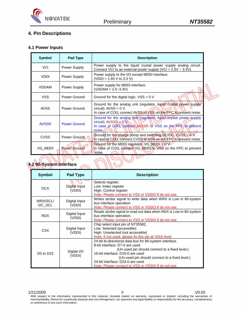
4. Pin Descriptions
4.1 Power Inputs
Symbol Pad Type Description
VCI Power Supply Power supply to the liquid crystal power supply analog circuit. Connect VCI to an external power supply (VCI = 2.5V ~ 3.3V).
VDDI Power Supply Power supply to the I/O except MDDI interface. (VDDI = 1.65 V to 3.3 V).
VDDAM Power Supply Power supply for MDDI interface. (VDDAM = 2.5~3.3V)
VSS Power Ground Ground for the digital logic. VSS = 0 V
AVSS Power Ground Ground for the analog unit (regulator, liquid crystal power supply circuit). AVSS = 0 V. In case of COG, connect AVSS to VSS on the FPC to prevent noise.
AVSSR Power Ground
Ground for the analog unit (regulator, liquid crystal power supply circuit). AVSSR = 0 V. In case of COG, connect AVSSR to VSS on the FPC to prevent noise.
CVSS Power Ground Ground for the charge pump and switching DC/DC. CVSS = 0 V. In case of COG, connect CVSS to VSS on the FPC to prevent noise.
VG_MDDI Power Ground Ground for the MDDI regulator. VG_MDDI = 0 V. In case of COG, connect VG_MDDI to VSS on the FPC to prevent noise.
4.2 80-System Interface
Symbol Pad Type Description
DCX Digital Input (VDDI)
Selects register. Low: Index register High: Control register Note: Please connect to VSS or VSSIO if do not use.
WRX/SCL/ I2C_SCL
Digital Input (VDDI)
Writes strobe signal to write data when WRX is Low in 80-system bus interface operation. Note: Please connect to VSS or VSSIO if do not use.
RDX Digital Input (VDDI)
Reads strobe signal to read out data when RDX is Low in 80-system bus interface operation. Note: Please connect to VSS or VSSIO if do not use.
CSX Digital Input (VDDI)
Chip select input pin of NT35582. Low: Selected (accessible) High: Unselected (not accessible) Note: If not used, please fix this pin at VDDI level.
D0 to D23 Digital I/O (VDDI)
24-bit bi-directional data bus for 80-system interface. 8-bit interface: D7-0 are used
(Un-used pin should connect to a fixed level.) 16-bit interface: D15-0 are used
(Un-used pin should connect to a fixed level.) 24-bit interface: D23-0 are used Note: Please connect to VSS or VSSIO if do not use.

Preliminary NT35582
1/21/2009 10 V0.02 With respect to the information represented in this material, Novatek makes no warranty, expressed or implied, including the warranties of merchantability, fitness for a particular purpose and non-infringement, nor assumes any legal liability or responsibility for the accuracy, completeness, or usefulness of any such information.
4.3 SPI Interface
Symbol Pad Type Description
CSX Digital Input (VDDI)
Chip select input pin of NT35582. Low: Selected (accessible) High: Unselected (not accessible) Note: If not used, please fix this pin at VDDI level.
WRX/SCL/ I2C_SCL
Digital Input (VDDI)
SCL: A synchronous clock signal in serial interface operation Note: Please connect to VSS or VSSIO if do not use.
SDI/ I2C_SDA Digital Input (VDDI)
SDI: Serial data input pin (SDI) in serial interface operation. The data is inputted on the rising or falling edge of the SCL signal by IM3 setting.
Note: Please connect to VSS or VSSIO if do not use.
SDO Digital Output (VDDI)
Serial data output pin (SDO) in serial interface operation. The data is outputted on the falling edge of the SCL signal. If the host places the SDI line into high-impedance state during the read intervals, the SDI and SDO can be tied together. Note: If not used, please open this pin.
4.4 I2C Interface
Symbol Pad Type Description
WRX/SCL/ I2C_SCL
Digital Input (VDDI)
I2C_SCL: Serial input clock in I2C-Bus interface operation. Note: Please connect to VSS or VSSIO if do not use.
SDI/ I2C_SDA Digital Input (VDDI)
I2C_SDA: Serial input/output data in I2C-Bus interface operation. Note: Please connect to VSS or VSSIO if do not use.
4.5 RGB Interface
Symbol Pad Type Description
DE Digital Input (VDDI)
Data enable signal in RGB I/F mode. Note: Please connect to VSS or VSSIO if do not use.
PCLK Digital Input (VDDI)
Pixel clock signal in RGB I/F mode Note: Please connect to VSS or VSSIO if do not use.
HS Digital Input (VDDI)
Horizontal sync. signal in RGB I/F mode Note: Please connect to VSS or VSSIO if do not use.
VS Digital Output (VDDI)
Vertical sync. Signal in RGB I/F mode. Note: Please connect to VSS or VSSIO if do not use.
D0~D23 Digital Output (VDDI)
24-bit data bus for RGB I/F mode. Data bus is share with 80-system interface. Note: Please connect to VSS or VSSIO if do not use.
SHUT Digital Output (VDDI)
Display on/off hardware pin in RGB I/F(only for RGB mode) -SHUT=1 sleep in mode
-SHUT=0 normal operation mode
SHUT COMMAND STATUS 1100h Sleep out mode 1 1000h Sleep in mode 1100h Sleep out mode
0 1000h Sleep out mode
-This function only viable in RGB mode. Note: If not used, please fix this pin at VDDI level.

Preliminary NT35582
1/21/2009 11 V0.02 With respect to the information represented in this material, Novatek makes no warranty, expressed or implied, including the warranties of merchantability, fitness for a particular purpose and non-infringement, nor assumes any legal liability or responsibility for the accuracy, completeness, or usefulness of any such information.
4.6 MDDI Interface
Symbol Pad Type Description
MDDI_STB_P MDDI Input (VDDAM)
MDDI positive strobe signal line. MDDI_STB_P/M are differential small amplitude signals. Ensure the wiring is shortest so that the COG resistance is less than 10 ohm. Note: Connect to VG_MDDI if do not use.
MDDI_STB_M MDDI Input (VDDAM)
MDDI negative strobe signal line. MDDI_STB_P/M are differential small amplitude signals. Ensure the wiring is shortest so that the COG resistance is less than 10 ohm. Note: Connect to VG_MDDI if do not use.
MDDI_DATA_P MDDI I/O (VDDAM)
MDDI positive data signal line. MDDI_DATA_P/M are differential small amplitude signals. Ensure the wiring is shortest so that the COG resistance is less than 10 ohm. Note: Connect to VG_MDDI if do not use.
MDDI_DATA_M MDDI I/O (VDDAM)
MDDI negative data signal line. MDDI_DATA_P/M are differential small amplitude signals. Ensure the wiring is shortest so that the COG resistance is less than 10 ohm. Note: Connect to VG_MDDI if do not use.
4.7 CABC+LABC Control Pins
Symbol Pad Type Description
LED_ON Digital Output (VDDI or VCC)
- This pin is connected to the external LED driver. - It is a LED driver control signal which is used for turning ON/OFF the LED backlight
- The amplitude of the LEDON signal is VDDI-VSS or VCI-VSS (Selected by CLED_VOL bit) Note: If not used, please open this pin.
LED_PWM Digital Output
(VDDI or VCC)
- This pin is connected to the external LED driver - PWM type control signal for brightness of the LED backlight - The width of this PWM signal is set from 256 values between 0% (LOW) and 100%(HIGH)
- The amplitude of the PWM signal is VDDI-VSS or VCI-VSS (Selected by CLED_VOL bit) Note: If not used, please open this pin.
ALS Analog Input Ambient light information from light sensor input pin. Note: Please connect to VSS or VSSIO if do not use.

Preliminary NT35582
1/21/2009 12 V0.02 With respect to the information represented in this material, Novatek makes no warranty, expressed or implied, including the warranties of merchantability, fitness for a particular purpose and non-infringement, nor assumes any legal liability or responsibility for the accuracy, completeness, or usefulness of any such information.
4.8 Interface Logic Pins
Symbol Pad Type Description
IM2-0* Digital Input (VDDI)
Selects the interface to MPU (VDDI-VSS amplitude signal).
IM2 IM1 IM0 System Interface Data Pin Colors
0 0 0 80-system 8-bit interface D7-0 65k, 262k, 16.7M
0 0 1 80-system 16-bit interface D15-0 65k, 262k, 16.7M
0 1 0 80-system 24-bit interface D23-0 65k, 262k, 16.7M
0 1 1 Serial interface SDI, SDO 65k, 262k, 16.7M
1 0 0 RGB+SPI interface D23-0 65k, 262k, 16.7M
1 0 1
MDDI + SPI/ I2C interface (4E00h_SPI_I2C bit = 0,
MDDI+SPI ; 4E00h_SPI_I2C bit=
1,MDDI+ I2C)
MDDI 65k, 262k, 16.7M
1 1 0 RGB+I2C interface D23-0 65k, 262k, 16.7M
1 1 1 MDDI+I2C interface MDDI 65k, 262k, 16.7M
IM3* Digital Input (VDDI)
For serial interface, RGB+SPI interface and MDDI+SPI interface setting only.
IM3 SCL Trigger Edge 0 Rising Edge 1 Falling Edge
Note: Please connect to VSS or VSSIO if do not use.
RESX* Digital Input (VDDI)
RESX pin. The LSI is initialized when RESX is Low. Make sure to execute a power-on reset after turning on power supply. There is no internal pull high resistor for this pin.
FTE* Digital Output (VDDI)
Frame head pulse signal. Utilize this signal when synchronizing RAM data write operations.
PNL* Digital Input (VDDI)
Select the panel type. - PNL=”0”, PMOS type - PNL=”1”, CMOS type
GM2-0* Digital Input (VDDI)
Select the resolution of NT35582 GM2-0 Resolution
000 480RGBx864 (Output: SDUM0, SDUM1,S1- S480, SDUM2) 001 480RGBx800 (Output: SDUM0, SDUM1,S1- S480, SDUM2) 010 480RGBx640 (Output: SDUM0, SDUM1,S1- S480, SDUM2) 011 Reserved 100 480RGBx864 (Output: SDUM3, SDUM2,S480- S1, SDUM1) 101 480RGBx800 (Output: SDUM3, SDUM2,S480- S1, SDUM1) 110 480RGBx640 (Output: SDUM3, SDUM2,S480- S1, SDUM1) 111 Reserved
SA1-0* Digital Input (VDDI)
Select the I2C interface Address from MPU SA1 SA0 Slave address Notes
0 0 1001100 0 1 1001101 1 0 1001110 1 1 1001111
0000xxx and 1111xxx: Reversed for special function
*Note: Please connect to VSS or VSSIO if do not use.

Preliminary NT35582
1/21/2009 13 V0.02 With respect to the information represented in this material, Novatek makes no warranty, expressed or implied, including the warranties of merchantability, fitness for a particular purpose and non-infringement, nor assumes any legal liability or responsibility for the accuracy, completeness, or usefulness of any such information.
Symbol Pad Type Description
NBWSEL Digital Input (VDDI)
Select the panel type NB or NW. NBWSEL NB/NW panel type selection
0 NW (Normally White) 1 NB (Normally Black)
Note: Please connect to VSS or VSSIO if do not use.
FRM Digital Input (VDDI)
This pin can select the free running mode for burn-in test. The display data alternates between full black and full white independent of input data in free running mode. - FRM = ’0’, Normal operation mode - FRM = ’1’, Free running mode
Note: Please connect to VSS or VSSIO if do not use.
RL Digital Input (VDDI)
Module source output direction H/W select pin GM2_0 RL Module source output direction
0 Display Data S1 -> S480 000,001,010 1 Display Data S480 -> S1 0 Display Data S480 -> S1 100,101,110 1 Display Data S1 -> S480
Note: Please connect to VSS or VSSIO if do not use.
TB Digital Input (VDDI)
-Module Gate output direction H/W select pin GM2_0 TB CMOS PMOS
0 U2D=VGH D2U= VGL
U2D= VGL D2U= VGH 000
100 1 U2D= VGL D2U= VGH
U2D= VGH D2U= VGL
0 U2D=VGH D2U= VGL
U2D= VGL D2U= VGH 001
101 1 U2D= VGL D2U= VGH
U2D= VGH D2U= VGL
0 U2D=VGH D2U= VGL
U2D= VGL D2U= VGH 010
110 1 U2D= VGL D2U= VGH
U2D= VGH D2U= VGL
Note: Please connect to VSS or VSSIO if do not use.

Preliminary NT35582
1/21/2009 14 V0.02 With respect to the information represented in this material, Novatek makes no warranty, expressed or implied, including the warranties of merchantability, fitness for a particular purpose and non-infringement, nor assumes any legal liability or responsibility for the accuracy, completeness, or usefulness of any such information.
4.9 Display Drive Analog Outputs
Symbol Pad Type Description
S1 to S480 Analog Output (AVDD/AVEE)
Liquid crystal application voltage output lines. The shift direction of the segment signal output can be reversed by setting the GM2 pin.
SDUM3,SDUM2, SDUM1,SDUM0,
Analog Output (AVDD/AVEE)
Liquid crystal application voltage output lines for Zigzag drive method. The shift direction of the segment signal output can be reversed by setting the GM2 pin.
4.10 Display Drive digital Outputs
Symbol Pad Type Description
SOUT1 (U2D)
Analog Output (VGH/VGL) Gate driver scan direction control signal
SOUT2 (D2U)
Analog Output (VGH/VGL) Inversed signal of SOUT1(T2B/U2D) for scan driver
SOUT3 (STV)
Analog Output (VGH/VGL) Gate driver start signal
SOUT4 (CLK)
Analog Output (VGH/VGL) Gate driver clock signal
SOUT5 (XCLK)
Analog Output (VGH/VGL) Inversed signal of SOUT4(CLK) for Gate driver
SOUT6 (RSW1/SW1)
Analog Output (VGH/VGL) RGB select signal
SOUT7 (GSW1/SW2)
Analog Output (VGH/VGL) RGB select signal
SOUT8 (BSW1/SW3)
Analog Output (VGH/VGL) RGB select signal
SOUT9 (XDON)
Analog Output (VGH/VGL) Control signal for abnormal power off
SOUT10 ~15 (CTRL1~6)
Analog Output (VGH/VGL)
Control signal for Cell test. DC level. VGH (PMOS) ; VGL(CMOS)
Preliminary NT35582
1/21/2009 15 V0.02 With respect to the information represented in this material, Novatek makes no warranty, expressed or implied, including the warranties of merchantability, fitness for a particular purpose and non-infringement, nor assumes any legal liability or responsibility for the accuracy, completeness, or usefulness of any such information.
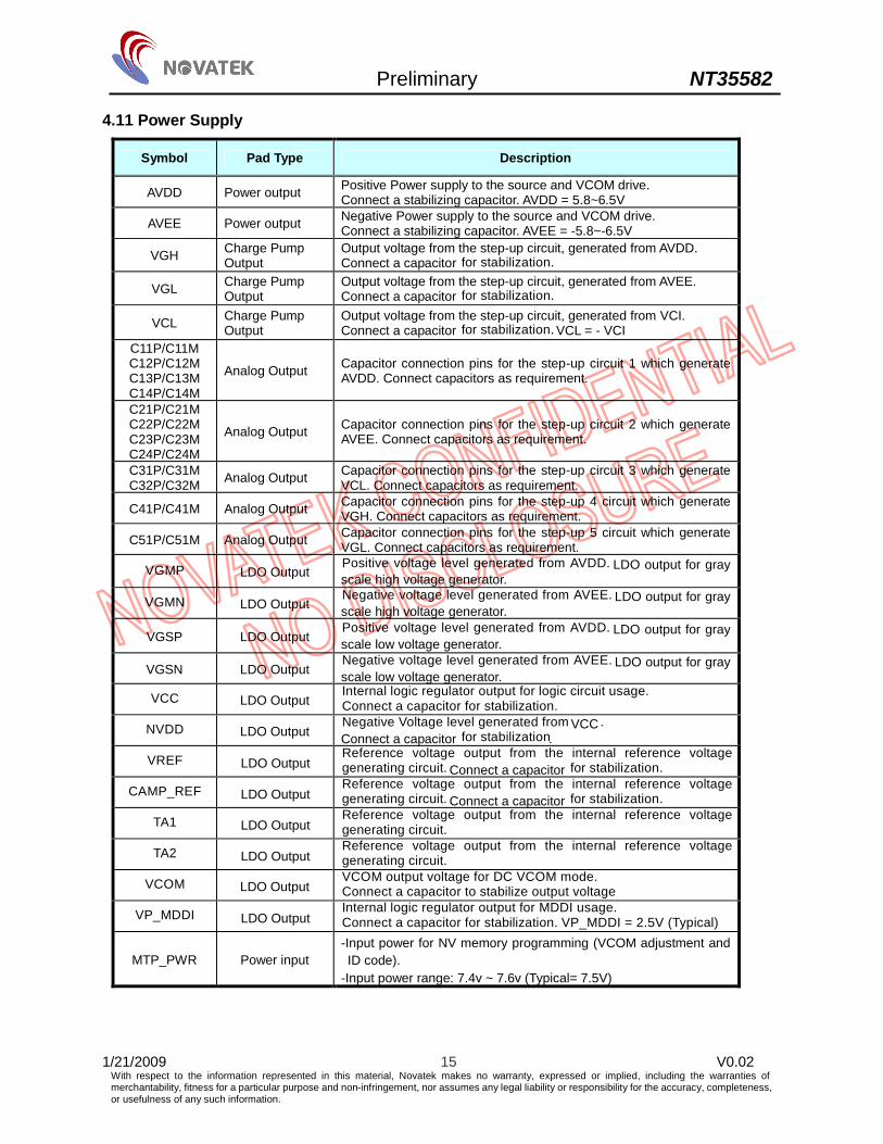
4.11 Power Supply
Symbol Pad Type Description
AVDD Power output Positive Power supply to the source and VCOM drive. Connect a stabilizing capacitor. AVDD = 5.8~6.5V
AVEE Power output Negative Power supply to the source and VCOM drive. Connect a stabilizing capacitor. AVEE = -5.8~-6.5V
VGH Charge Pump Output
Output voltage from the step-up circuit, generated from AVDD. Connect a capacitor for stabilization.
VGL Charge Pump Output
Output voltage from the step-up circuit, generated from AVEE. Connect a capacitor for stabilization.
VCL Charge Pump Output
Output voltage from the step-up circuit, generated from VCI. Connect a capacitor for stabilization. VCL = - VCI
C11P/C11M C12P/C12M C13P/C13M C14P/C14M
Analog Output Capacitor connection pins for the step-up circuit 1 which generate AVDD. Connect capacitors as requirement.
C21P/C21M C22P/C22M C23P/C23M C24P/C24M
Analog Output Capacitor connection pins for the step-up circuit 2 which generate AVEE. Connect capacitors as requirement.
C31P/C31M C32P/C32M Analog Output Capacitor connection pins for the step-up circuit 3 which generate
VCL. Connect capacitors as requirement.
C41P/C41M Analog Output Capacitor connection pins for the step-up 4 circuit which generate VGH. Connect capacitors as requirement.
C51P/C51M Analog Output Capacitor connection pins for the step-up 5 circuit which generate VGL. Connect capacitors as requirement.
VGMP LDO Output Positive voltage level generated from AVDD. LDO output for gray scale high voltage generator.
VGMN LDO Output Negative voltage level generated from AVEE. LDO output for gray scale high voltage generator.
VGSP LDO Output Positive voltage level generated from AVDD. LDO output for gray scale low voltage generator.
VGSN LDO Output Negative voltage level generated from AVEE. LDO output for gray scale low voltage generator.
VCC LDO Output Internal logic regulator output for logic circuit usage. Connect a capacitor for stabilization.
NVDD LDO Output Negative Voltage level generated from VCC . Connect a capacitor for stabilization.
VREF LDO Output Reference voltage output from the internal reference voltage generating circuit. Connect a capacitor for stabilization.
CAMP_REF LDO Output Reference voltage output from the internal reference voltage generating circuit. Connect a capacitor for stabilization.
TA1 LDO Output Reference voltage output from the internal reference voltage generating circuit.
TA2 LDO Output Reference voltage output from the internal reference voltage generating circuit.
VCOM LDO Output VCOM output voltage for DC VCOM mode. Connect a capacitor to stabilize output voltage
VP_MDDI LDO Output Internal logic regulator output for MDDI usage. Connect a capacitor for stabilization. VP_MDDI = 2.5V (Typical)
MTP_PWR Power input -Input power for NV memory programming (VCOM adjustment and ID code).
-Input power range: 7.4v ~ 7.6v (Typical= 7.5V)

Preliminary NT35582
1/21/2009 16 V0.02 With respect to the information represented in this material, Novatek makes no warranty, expressed or implied, including the warranties of merchantability, fitness for a particular purpose and non-infringement, nor assumes any legal liability or responsibility for the accuracy, completeness, or usefulness of any such information.
4.12 Test Pins (Test and Dummy pins)
Symbol Pad Type Description
TEST - Test pin not accessible to user; Connect to VSS or VSSIO.
OSC - Test pin not accessible to user; Connect to VSS or VSSIO.
Dummy0~ Dummy 24 - - These pins are dummy (possess no function inside)
- Dummy pins are not accessible to user. Must be left open.
VDDIO Output VDDI voltage output level for control pin used.
VSSIO Output VSS voltage output level for control pin used.

Preliminary NT35582
1/21/2009 17 V0.02 With respect to the information represented in this material, Novatek makes no warranty, expressed or implied, including the warranties of merchantability, fitness for a particular purpose and non-infringement, nor assumes any legal liability or responsibility for the accuracy, completeness, or usefulness of any such information.
5. FUNCTION DESCRIPTION
5.1 MPU INTERFACE NT35582 can interface with MPU at high speed. However, if the interface cycle time is faster than the limit, MPU needs to have dummy wait(s) to meet the cycle time limit.
5.1.1 General Protocol
For programming of the LCD driver, the general supported protocol is shown in Fig. 2
S TB TB TB TB TB TB P
S: Start data tranamissionP: Stop data tranamissionTB: tranamission byte
Figure.2 Programming protocol

Preliminary NT35582
1/21/2009 18 V0.02 With respect to the information represented in this material, Novatek makes no warranty, expressed or implied, including the warranties of merchantability, fitness for a particular purpose and non-infringement, nor assumes any legal liability or responsibility for the accuracy, completeness, or usefulness of any such information.
5.1.2 80-System Interface The MCU uses a 11-wires 8-data parallel interface or 19-wires 16-data parallel interface or 27-wires 24-data parallel interface. The chip-select CSX (active low) enables and disables the parallel interface. WRX is the parallel data write, RDX is the parallel data read and D[23:0] is parallel data. The Graphics Controller Chip reads the data at the rising edge of WRX signal. The D/CX is the data/command flag. When D/CX=’1’, D[23:0] bits are display RAM data or command parameters. When D/C=’0’, D[23:0] bits are commands. The 8080-series bi-directional interface can be used for communication between the micro controller and LCD driver chip. Interface bus width can be selected by setting IM2, IM1 and IM0 as following table.
Table 5.1.1 The function of 80-series system interface IM2 IM1 IM0 Interface DCX RDX WRX Function
0 1 ↑ Write 16-bit command (D7 to D0)
1 1 ↑ Write 16/18/24-bit display data or 16-bit parameter (D7 to D0)
1 ↑ 1 Read 16/18/24-bit display data (D7 to D0) 0 0 0 8-bit
Parallel
1 ↑ 1 Read 16-bit parameter or status (D7 to D0) 0 1 ↑ Write 16-bit command (D15 to D0) 1 1 ↑ Write 16/18/24-bit display data or 16-bit parameter (D15 to D0) 1 ↑ 1 Read 16/18/24-bit display data (D15 to D0)
0 0 1 16-bit Parallel
1 ↑ 1 Read 16-bit parameter or status (D15 to D0) 0 1 ↑ Write 16-bit command (D23 to D0) 1 1 ↑ Write 16/18/24-bit display data or 16-bit parameter (D23 to D0) 1 ↑ 1 Read 16/18/24-bit display data (D23 to D0)
0 1 0 24-bit Parallel
1 ↑ 1 Read 16-bit parameter or status (D23 to D0)

Preliminary NT35582
1/21/2009 19 V0.02 With respect to the information represented in this material, Novatek makes no warranty, expressed or implied, including the warranties of merchantability, fitness for a particular purpose and non-infringement, nor assumes any legal liability or responsibility for the accuracy, completeness, or usefulness of any such information.
5.1.2.1 Write cycle sequence
The write cycle means that the host writes information (command or/and data) to the display via the interface. Each write cycle (WRX high-low-high sequence) consists of 3 control (D/CX, RDX, WRX) and data signals (D[23:0]). D/CX bit is a control signal, which tells if the data is a command or a ram data. The data signals represent the command if the control signal is low (=’0’) and vice versa it is data (=’1’).
Figure.3 80-Series WRX Protocol
S CMD CMD PA1 CMD PAn-2 PAn-1 PPA1
CMD CMD PA1 CMD PAn-2PA1
CMD CMD PA1 CMD PAn-2PA1
PAn-1
PAn-1
Hi-Z
Host D[23:0](MPU to LCD)
Driver D[23:0](LCD to MPU)
D[23:0]
WRX
RDX
D/CX
CSX
CMD: Write command codePA: Write parameter or RAM data
Signals on D[23:0], D/CX, RDX and WRX pinsduring CSX=” H” are ignored
1-byte command
2-byte command n-byte command (number of parameter = n-1)
Figure.4 80-Series parallel bus protocol, write to register or display RAM
WRX
D[23:0]
The host starts to controlD[23:0] lines when there isa falling edge of the WRX
The display reads D[23:0]lines when there is a
rising edge of the WRX
The host stops tocontrol D[23:0]
lines

Preliminary NT35582
1/21/2009 20 V0.02 With respect to the information represented in this material, Novatek makes no warranty, expressed or implied, including the warranties of merchantability, fitness for a particular purpose and non-infringement, nor assumes any legal liability or responsibility for the accuracy, completeness, or usefulness of any such information.
5.1.2.2 Read Cycle Sequence
The read cycle (RDX high-low-high sequence) means that the host reads information from display via interface. The display sends data (D[23:0]) to the host when there is a falling edge of RDX and the host reads data when there is a rising edge of RDX.
RDX
D[23:0]
The display starts tocontrol D[23:0] lines
when there is a fallingedge of the RDX
The host reads D[23:0]lines when there is arising edge of RDX
The display stops tocontrol D[23:0]
Figure.5 80-Series RDX Protocol
S CMD PA CMD DM P
CMD CMD
CMD CMD
Hi-Z
Host D[23:0]( MPU to LCD )
Driver D[ 23:0]( LCD to MPU )
D[ 23:0]
WRX
RDX
DCX
CSX
CMD: Write command codePA : Write parameter or RAM data
Signals on D [23:0] , DCX , RDX and WRX pinsduring CSX = ” H” are ignored
Read parameter Read display RAM data
Data
PA DM PA
PA
Hi-Z
Hi-Z
Hi-Z
DM PAHi-ZHi-Z
Figure.6 80-Series parallel bus protocol, read from register

Preliminary NT35582
1/21/2009 21 V0.02 With respect to the information represented in this material, Novatek makes no warranty, expressed or implied, including the warranties of merchantability, fitness for a particular purpose and non-infringement, nor assumes any legal liability or responsibility for the accuracy, completeness, or usefulness of any such information.
5.1.3 Serial Interface
The selection of this interface is done by set IM2/1/0 = 3’b011. And select IM3 = 0 or 1 to decide the trigger edge of serial clock (SCL) is rising edge or falling edge while IM[2:0] setting is 3’b100 or 3’b101.
The serial interface is used to communication between the micro controller and the LCD driver chip. It contains CSX (chip select), SCL (serial clock), SDI (serial data input) and SDO (serial data output). Serial clock (SCL) is used for interface with MPU only, so it can be stopped when no communication is necessary.
If the host places the SDI line into high-impedance state during the read intervals, the SDI and SDO can be tied together.
5.1.3.1 Write Mode
The write mode of the interface means the micro controller writes commands and data to the NT35582.
Any instruction can be sent in any order to the NT35582. The MSB is transmitted first. The serial interface is initialized when CSX is high. In this state, SCL clock pulse or SDI data have no effect. A falling edge on CSX enables the serial interface and indicates the start of data transmission.
R/W D/CX H/L 0 0 0 0 0 ADD[15]
ADD[14]
ADD[13]
ADD[12]
ADD[11]
ADD[10]
ADD[9]
ADD[8] R/W D/CX H/L
CSX (Host to Driver IC)
SCL ( Host to Driver IC)
(Rising Edge, IM3 = 0)
SDI (Host to Driver IC)
SDO (Driver IC to Host)High-Z High-Z High-Z
S P STransmission Byte Transmission ByteFirst Transmit
R/ W = ‘ 0’ for Writing Command / AddressD/ CX = ‘ 0 ' for Command / Address Transmission
SCL (Host to Driver IC)
(Falling Edge , IM3 = 1)
8-bit 8-bit
H/ L = ‘ 1 ' for Command / Address High Byte Transmission
Figure.7-1 Serial bus protocol, register write mode (first transmit)
R/W D/CX H/L 0 0 0 0 0 ADD[7]
ADD[6]
ADD[5]
ADD[4]
ADD[3]
ADD[2]
ADD[1]
ADD[0] R/W D/CX H/L
CSX (Host to Driver IC)
SCL (Host to Driver IC)
(Rising Edge, IM3 = 0)
SDI (Host to Driver IC)
SDO (Driver IC to Host)High-Z High-Z High-Z
S P STransmission Byte Transmission ByteSecond
Transmit
R/ W = ‘ 0’ for Writing Command / AddressD/ CX = ‘ 0 ' for Command / Address Transmission
SCL (Host to Driver IC)
(Falling Edge , IM3 = 1)
8-bit 8-bit
H/ L = ‘ 0 ' for Command / Address Low Byte Transmission
Figure.7-2 Serial bus protocol, register write mode (second transmit)

Preliminary NT35582
1/21/2009 22 V0.02 With respect to the information represented in this material, Novatek makes no warranty, expressed or implied, including the warranties of merchantability, fitness for a particular purpose and non-infringement, nor assumes any legal liability or responsibility for the accuracy, completeness, or usefulness of any such information.
R/W D/CX 0 0 0 0 0 0 D[7]
D[6]
D[5]
D[4]
D[3]
D[2]
D[1]
D[0] R/W D/CX H/L
High-Z High-Z High-Z
S P STransmission Byte Transmission Byte
R/ W = ‘ 0’ for Writing Parameter / DataD/ CX = ‘ 1 ' for Parameter / Data Transmission
CSX (Host to Driver IC)
SCL (Host to Driver IC)
(Rising Edge, IM3 = 0)
SDI (Host to Driver IC)
SDO (Driver IC to Host)
SCL (Host to Driver IC)
( Falling Edge, IM3 = 1)
8-bit 8-bit
Third Transmit
H/ L = ‘ 0 ' for Parameter / Data Low Byte Transmission
Figure.7-3 Serial bus protocol, register write mode (third transmit)
R/W D/CX H/L 0 0 0 0 0 ADD[15]
ADD[14]
ADD[13]
ADD[12]
ADD[11]
ADD[10]
ADD[9]
ADD[8] R/W D/CX H/L
CSX (Host to Driver IC)
SDI (Host to Driver IC)
SDO (Driver IC to Host)High-Z High-Z High-Z
S P STransmission Byte Transmission ByteFirst Transmit
R/ W = ‘ 0’ for Writing Command / AddressD/ CX = ‘ 0 ' for Command / Address Transmission
8-bit 8-bit
H/ L = ‘ 1 ' for Command / Address High Byte Transmission
Figure.8-1 Serial bus protocol, RAM write mode (first transmit)
R/W D/CX H/L 0 0 0 0 0 ADD[7]
ADD[6]
ADD[5]
ADD[4]
ADD[3]
ADD[2]
ADD[1]
ADD[0] R/W D/CX H/L
CSX (Host to Driver IC)
SDI (Host to Driver IC)
SDO (Driver IC to Host)High-Z High-Z High-Z
S P STransmission Byte Transmission ByteSecond
Transmit
R/ W = ‘ 0’ for Writing Command / AddressD/ CX = ‘ 0 ' for Command / Address Transmission
8-bit 8-bit
H/ L = ‘ 0 ' for Command / Address Low Byte Transmission
Figure.8-2 Serial bus protocol, RAM write mode (second transmit)

Preliminary NT35582
1/21/2009 23 V0.02 With respect to the information represented in this material, Novatek makes no warranty, expressed or implied, including the warranties of merchantability, fitness for a particular purpose and non-infringement, nor assumes any legal liability or responsibility for the accuracy, completeness, or usefulness of any such information.
R/W D/CX 0 0 0 0 0 0 x x x R1[4]
R1[3]
R1[2]
R1[1]
R1[0] R/W D/CX 0
CSX (Host)
SCL (Host)
SDI (Host )
SDO (Driver IC) High-Z High-Z High-Z
S P STransmission Byte Transmission Byte
R/ W = ‘ 0 ’ for Write OperationD/ CX = ‘ 1 ' for Data Transmission
Third Transmit
Figure.8-3 Serial bus protocol, RAM write mode (third transmit)
R/W D/CX 0 0 0 0 0 0 x x G1[5]
G1[4]
G1[3]
G1[2]
G1[1]
G1[0] R/W D/CX 0SDI (Host)
CSX (Host)
SCL (Host)
SDO (Driver IC) High-Z High-Z High-Z
S P STransmission Byte Transmission Byte
R/ W = ‘ 0 ’ for Write OperationD/ CX = ‘ 1 ' for Data Transmission
Forth Transmit
Figure.8-4 Serial bus protocol, RAM write mode (forth transmit)
0
CSX (Host)
SCL (Host)
SDO (Driver IC) High-Z High-Z High-Z
S P STransmission Byte Transmission Byte
R/ W = ‘ 0 ’ for Write OperationD/ CX = ‘ 1 ' for Data Transmission
Fifth Transmit
R/W D/CX 0 0 0 0 0 0 x x x B1[4]
B1[3]
B1[2]
B1[1]
B1[0] R/W D/CX 0SDI (Host)
Figure.8-5 Serial bus protocol, RAM write mode (fifth transmit)
Preliminary NT35582
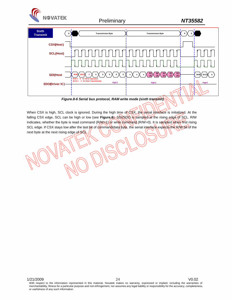
1/21/2009 24 V0.02 With respect to the information represented in this material, Novatek makes no warranty, expressed or implied, including the warranties of merchantability, fitness for a particular purpose and non-infringement, nor assumes any legal liability or responsibility for the accuracy, completeness, or usefulness of any such information.
Sixth Transmit
0
CSX (Host)
SCL (Host)
SDO (Driver IC) High-Z High-Z High-Z
S P STransmission Byte Transmission Byte
R/ W = ‘ 0 ’ for Write OperationD/ CX = ‘ 1 ' for Data Transmission
0SDI (Host R/W D/CX 0 0 0 0 0 0 x x R2[4]
R2[3]
R2[2]
R2[1]
R2[0] R/W D/CX 0x
Figure.8-6 Serial bus protocol, RAM write mode (sixth transmit)
When CSX is high, SCL clock is ignored. During the high time of CSX, the serial interface is initialized. At the falling CSX edge, SCL can be high or low (see Figure.6). SDI/SDO is sampled at the rising edge of SCL. R/W indicates, whether the byte is read command (R/W=1) or write command (R/W=0). It is sampled when first rising SCL edge. If CSX stays low after the last bit of command/data byte, the serial interface expects the R/W bit of the next byte at the next rising edge of SCL.

Preliminary NT35582
1/21/2009 25 V0.02 With respect to the information represented in this material, Novatek makes no warranty, expressed or implied, including the warranties of merchantability, fitness for a particular purpose and non-infringement, nor assumes any legal liability or responsibility for the accuracy, completeness, or usefulness of any such information.
5.1.3.2 Read Mode
The read mode of the interface means that the micro controller reads register value from the NT35582. To do so the micro controller first has to send a command and then the following byte is transmitted in the opposite direction. After that CSX is required to go high before a new command is sent (see Fig.9). The NT35582 samples the SDI (input data) at the rising edges, but shifts SDO (output data) at the falling SCL edges. Thus the micro controller is supported to read data at the rising SCL edges.
After the read status command has been sent, the SDI line must be set to tri-state no later than at the falling SCL edge of the last bit.
For the memory data read, a dummy clock cycle is needed (16 SCL clocks) to wait the memory data sent out in SPI interface. But it doesn’t need any dummy clock when execute the command data read.
R/W D/CX H/L 0 0 0 0 0 ADD[15]
ADD[14]
ADD[13]
ADD[12]
ADD[11]
ADD[10]
ADD[9]
ADD[8] R/W D/CX H/L
CSX (Host to Driver IC)
SCL ( Host to Driver IC )
(Rising Edge , IM 3 = 0)
SDI (Host to Driver IC )
SDO (Driver IC to Host )High-Z High-Z High-Z
S P STransmission Byte Transmission ByteFirst Transmit
R/ W = ‘ 0’ for Writing Command / AddressD/ CX = ‘ 0 ' for Command / Address Transmission
SCL (Host to Driver IC )
( Falling Edge , IM3 = 1)
8-bit 8-bit
H/ L = ‘ 1 ' for Command / Address High Byte Transmission
Figure.9-1 Serial bus protocol, register read mode (First transmit)
R/W D/CX H/L 0 0 0 0 0 ADD[ 7]
ADD[6]
ADD[5]
ADD[4]
ADD[3]
ADD[2]
ADD[1]
ADD[0] R/W D/CX H/L
CSX (Host to Driver IC )
SCL (Host to Driver IC )
(Rising Edge , IM 3 = 0)
SDI (Host to Driver IC )
SDO (Driver IC to Host )High-Z High-Z High-Z
S P STransmission Byte Transmission ByteSecond
Transmit
R/ W = ‘ 0’ for Writing Command / AddressD/ CX = ‘ 0 ' for Command / Address Transmission
SCL ( Host to Driver IC )
(Falling Edge , IM 3 = 1)
8-bit 8-bit
H/ L = ‘ 0 ' for Command / Address Low Byte Transmission
Figure.9-2 Serial bus protocol, register read mode (Second transmit)

Preliminary NT35582
1/21/2009 26 V0.02 With respect to the information represented in this material, Novatek makes no warranty, expressed or implied, including the warranties of merchantability, fitness for a particular purpose and non-infringement, nor assumes any legal liability or responsibility for the accuracy, completeness, or usefulness of any such information.
Third Transmit
R/W D/CX 0 0 0 0 0 0
D[7]
D[6]
D[5]
D[4]
D[3]
D[2]
D[1]
D[0]
R/W D/CX 0SDI (Host)
SDO (Driver IC)High-Z High-Z
R/ W = ‘ 1’ for Read OperationD/ CX = ‘ 1 ' for Data Transmission
High-Z
CSX (Host to Driver IC )
SCL (Host to Driver IC )
(Rising Edge , IM 3 = 0)
S P STransmission Byte Transmission Byte
SCL ( Host to Driver IC )
(Falling Edge , IM3 = 1)
8-bit 8-bit
Figure.9-3 Serial bus protocol, register read mode (third transmit)

Preliminary NT35582
1/21/2009 27 V0.02 With respect to the information represented in this material, Novatek makes no warranty, expressed or implied, including the warranties of merchantability, fitness for a particular purpose and non-infringement, nor assumes any legal liability or responsibility for the accuracy, completeness, or usefulness of any such information.
5.1.4 Data Transfer Pause
By using parallel interface, it is possible when transferring a Command, Frame Memory Data or Multiple Parameter Data to invoke a pause in the data transmission. If the Chip Select Line is released after a whole byte of a Frame Memory Data or Multiple Parameter Data has been completed, NT35582 will wait and continue the Frame Memory Data or Parameter Data Transmission from the point where it was paused. If the Chip Select Line is released after a whole byte of a command as been completed, the Display Module will receive either the command’s parameters (if appropriate) or a new command when the Chip Select Line is next enabled as shown below.
This applies to the following 4 conditions: 1) Command-Pause-Command 2) Command-Pause-Parameter 3) Parameter-Pause-Command 4) Parameter-Pause-Parameter
5.1.4.1 Parallel Interface Pause
D23 to D0 D23 to D0
Pause
PauseCommand /Parameter
Command /Parameter
CSX
D/CX
RDX
WRX
D[23:0]
Figure.10 Parallel bus protocol, write mode – paused by CSX
5.1.4.2 Serial Interface Pause SPI interface does NOT support “Pause mode”.

Preliminary NT35582
1/21/2009 28 V0.02 With respect to the information represented in this material, Novatek makes no warranty, expressed or implied, including the warranties of merchantability, fitness for a particular purpose and non-infringement, nor assumes any legal liability or responsibility for the accuracy, completeness, or usefulness of any such information.
5.1.5 Data Transfer Break and Recovery
If there is a break in data transmission by RESX pulse while transferring a Command or Frame Memory Data or Multiple Parameter command Data before Bit D0 of the byte has been completed, NT35582 will reject the previous bits and have reset the interface such that it will be ready to receive command data again when the chip select line (CSX) is next activated after RESX have been High state. See the following example (See Fig.11)
If there is a break in data transmission by CSX pulse while transferring a Command or Frame Memory Data or Multiple Parameter command Data before Bit D0 of the byte has been completed, NT35582 will reject the previous bits and have reset the interface such that it will be ready to receive the same byte re-transmitted when the chip select line (CSX) is next activated. See the following example (See Fig.12)
Figure.11 Serial bus protocol write mode – interrupted by RESX
Figure.12 Serial bus protocol write mode – interrupted by CSX

Preliminary NT35582
1/21/2009 29 V0.02 With respect to the information represented in this material, Novatek makes no warranty, expressed or implied, including the warranties of merchantability, fitness for a particular purpose and non-infringement, nor assumes any legal liability or responsibility for the accuracy, completeness, or usefulness of any such information.
5.1.6 Display Module Data Transfer Modes The Module has 4 color modes for transferring data to the display RAM. These are 12-bit color per pixel, 16-bit color per pixel, 18-bit color per pixel and 24-bit color per pixel. The data format is described for each interface. Data can be downloaded to the frame memory by 2 methods.
5.1.6.1 Method 1
The Image data is sent to the frame memory in successive frame writes, each time the frame memory is filled, the frame memory pointer is reset to the start point and the next frame is written.
Start FrameMemory
Write
ImageData
Frame 1
ImageData
Frame 2
ImageData
Frame 3
AnyCommand
Start Stop
Figure.13 Display module data transfer mode 1
5.1.6.2 Method 2
Image data is sent and at the end of each frame memory download, a command is sent to stop Frame Memory Write. Then Start Memory Write command is sent, and a new frame is downloaded.
Start FrameMemory
Write
ImageData
Frame 1
AnyCommand
Start
Stop
AnyCommand
Start FrameMemory
Write
ImageData
Frame 2
AnyCommand
Figure.14 Display module data transfer mode 2 Note: 1) These apply to all Data Transfer Color modes on both Serial and Parallel interfaces. 2) The Frame Memory can contain both odd and even number of pixels for both methods. Only complete pixel
data will be stored in the frame memory.

Preliminary NT35582
1/21/2009 30 V0.02 With respect to the information represented in this material, Novatek makes no warranty, expressed or implied, including the warranties of merchantability, fitness for a particular purpose and non-infringement, nor assumes any legal liability or responsibility for the accuracy, completeness, or usefulness of any such information.
5.2 DISPLAY DATA RAM (DDRAM) The NT35582 has an integrated 480x864x24-bit graphic type static RAM. This 1,244k-byte memory allows to store on-chip a 480xRGBx864 image with 24-bit resolution (16.7M-color). There will be no abnormal visible effect on the display when there is a simultaneous Panel Read and Interface Read or Write to the same location of the frame memory.
MPU I/F or MDDI I/F
RowAddress Counter
Column AddressCounter
Host Interface
Latch
Display Data RAM(480 x 864 x 24-bit)
ScanAddressCounter
LineAddressCounter
LCD Glass(480 x RGB x 864)
Figure.15 Display data RAM

Preliminary NT35582
1/21/2009 31 V0.02 With respect to the information represented in this material, Novatek makes no warranty, expressed or implied, including the warranties of merchantability, fitness for a particular purpose and non-infringement, nor assumes any legal liability or responsibility for the accuracy, completeness, or usefulness of any such information.
5.2.1 3-wire Serial Interface for DATA RAM write Different display data formats are available for four colors depth supported by the LCM listed below. -65K colors, RGB 5,6,5-bits input. -262K colors, RGB 6,6,6-bits input. -16.7M colors, RGB 8,8,8-bits input.
5.2.1.1 65K Colors (5-6-5 Bits Input)
R/W D/CX H/L 0 0 0 0 0 ADD[15]
ADD[14]
ADD[13]
ADD[12]
ADD[11]
ADD[10]
ADD[9]
ADD[8] R/W D/CX H/L
CSX (Host to Driver IC)
SDI (Host to Driver IC)
SDO (Driver IC to Host)High-Z High-Z High-Z
S P STransmission Byte Transmission ByteFirst Transmit
R/ W = ‘ 0’ for Writing Command / AddressD/ CX = ‘ 0 ' for Command / Address Transmission
8-bit 8-bit
H/ L = ‘ 1 ' for Command / Address High Byte Transmission
Figure.16-1 Serial bus protocol: SRAM write mode (5-6-5) (first transmit)
R/W D/CX H/L 0 0 0 0 0 ADD[7]
ADD[6]
ADD[5]
ADD[4]
ADD[3]
ADD[2]
ADD[1]
ADD[0] R/W D/CX H/L
CSX (Host to Driver IC)
SDI (Host to Driver IC)
SDO (Driver IC to Host)High-Z High-Z High-Z
S P STransmission Byte Transmission ByteSecond
Transmit
R/ W = ‘ 0’ for Writing Command / AddressD/ CX = ‘ 0 ' for Command / Address Transmission
8-bit 8-bit
H/ L = ‘ 0 ' for Command / Address Low Byte Transmission
Figure.16-2 Serial bus protocol: SRAM write mode (5-6-5) (second transmit)
R/W D/CX 0 0 0 0 0 0 x x x R1[4]
R1[3]
R1[2]
R1[1]
R1[0] R/W D/CX 0
CSX (Host)
SCL (Host)
SDI (Host )
SDO (Driver IC) High-Z High-Z High-Z
S P STransmission Byte Transmission Byte
R/ W = ‘ 0 ’ for Write OperationD/ CX = ‘ 1 ' for Data Transmission
Third Transmit
Figure.16-3 Serial bus protocol: SRAM write mode (5-6-5) (third transmit)

Preliminary NT35582
1/21/2009 32 V0.02 With respect to the information represented in this material, Novatek makes no warranty, expressed or implied, including the warranties of merchantability, fitness for a particular purpose and non-infringement, nor assumes any legal liability or responsibility for the accuracy, completeness, or usefulness of any such information.
R/W D/CX 0 0 0 0 0 0 x x G1[5]
G1[4]
G1[3]
G1[2]
G1[1]
G1[0] R/W D/CX 0SDI (Host)
CSX (Host)
SCL (Host)
SDO (Driver IC) High-Z High-Z High-Z
S P STransmission Byte Transmission Byte
R/ W = ‘ 0’ for Write OperationD/ CX = ‘ 1 ' for Data Transmission
Forth Transmit
Figure.16-4 Serial bus protocol: SRAM write mode (5-6-5) (fourth transmit)
0
CSX (Host)
SCL (Host)
SDO (Driver IC) High-Z High-Z High-Z
S P STransmission Byte Transmission Byte
R/ W = ‘ 0’ for Write OperationD/ CX = ‘ 1 ' for Data Transmission
Fifth Transmit
R/W D/CX 0 0 0 0 0 0 x x x B1[4]
B1[3]
B1[2]
B1[1]
B1[0] R/W D/CX 0SDI (Host)
Figure.16-5 Serial bus protocol: SRAM write mode (5-6-5) (fifth transmit)
Sixth
Transmit
0
CSX (Host)
SCL (Host)
SDO (Driver IC) High-Z High-Z High-Z
S P STransmission Byte Transmission Byte
R/ W = ‘ 0’ for Write OperationD/ CX = ‘ 1 ' for Data Transmission
0SDI (Host R/W D/CX 0 0 0 0 0 0 x x R2[4]
R2[3]
R2[2]
R2[1]
R2[0] R/W D/CX 0x
Figure.16-6 Serial bus protocol: SRAM write mode (5-6-5) (sixth transmit)

Preliminary NT35582
1/21/2009 33 V0.02 With respect to the information represented in this material, Novatek makes no warranty, expressed or implied, including the warranties of merchantability, fitness for a particular purpose and non-infringement, nor assumes any legal liability or responsibility for the accuracy, completeness, or usefulness of any such information.
5.2.1.2 262K Colors (6-6-6 Bits Input)
R/W D/CX H/L 0 0 0 0 0 ADD[15]
ADD[14]
ADD[13]
ADD[12]
ADD[11]
ADD[10]
ADD[9]
ADD[8] R/W D/CX H/L
CSX (Host to Driver IC)
SDI (Host to Driver IC)
SDO (Driver IC to Host)High-Z High-Z High-Z
S P STransmission Byte Transmission ByteFirst Transmit
R/ W = ‘ 0’ for Writing Command / AddressD/ CX = ‘ 0 ' for Command / Address Transmission
8-bit 8-bit
H/ L = ‘ 1 ' for Command / Address High Byte Transmission
Figure.17-1 Serial bus protocol: SRAM write mode (6-6-6) (first transmit)
R/W D/CX H/L 0 0 0 0 0 ADD[7]
ADD[6]
ADD[5]
ADD[4]
ADD[3]
ADD[2]
ADD[1]
ADD[0] R/W D/CX H/L
CSX (Host to Driver IC)
SDI (Host to Driver IC)
SDO (Driver IC to Host)High-Z High-Z High-Z
S P STransmission Byte Transmission ByteSecond
Transmit
R/ W = ‘ 0’ for Writing Command / AddressD/ CX = ‘ 0 ' for Command / Address Transmission
8-bit 8-bit
H/ L = ‘ 0 ' for Command / Address Low Byte Transmission
Figure.17-2 Serial bus protocol: SRAM write mode (6-6-6) (second transmit)
R/W D/CX 0 0 0 0 0 0 R/W D/CX 0
CSX ( Host)
SCL ( Host)
( Rising Edge, IM3 = 0)
SDI ( Host)
SDO ( Driver IC) High-Z High-Z
S P STransmission Byte Transmission Byte
R/ W = ‘ 0’ for Writing Parameter / DataD/ CX = ‘ 1' for Parameter / Data Transmission
SCL ( Host)
( Falling Edge, IM3 = 1)
High-Z
0 0 R1[5]
R1[4]
R1[3]
R1[2]
R1[1]
R1[0]
Third Transmit
Figure.17-3 Serial bus protocol: SRAM write mode (6-6-6) (third transmit)

Preliminary NT35582
1/21/2009 34 V0.02 With respect to the information represented in this material, Novatek makes no warranty, expressed or implied, including the warranties of merchantability, fitness for a particular purpose and non-infringement, nor assumes any legal liability or responsibility for the accuracy, completeness, or usefulness of any such information.
R/W D/CX 0 0 0 0 0 0 R/W D/CX 0
CSX ( Host)
SCL ( Host)
( Rising Edge, IM3 = 0)
SDI ( Host)
SDO ( Driver IC) High-Z High-Z
S P STransmission Byte Transmission Byte
R/ W = ‘ 0’ for Writing Parameter / DataD/ CX = ‘ 1 ' for Parameter / Data Transmission
SCL ( Host)
( Falling Edge, IM3 = 1)
0 0 G1[5]
G1[4]
G1[3]
G1[2]
G1[1]
G1[0]
High-Z
Forth Transmit
Figure.17-4 Serial bus protocol: SRAM write mode (6-6-6) (fourth transmit)
R/W D/CX 0 0 0 0 0 0 R/W D/CX 0
CSX ( Host)
SCL ( Host)
( Rising Edge, IM3 = 0)
SDI ( Host)
SDO ( Driver IC) High-Z High-Z
S P STransmission Byte Transmission Byte
R/ W = ‘ 0’ for Writing Parameter / DataD/ CX = ‘ 1' for Parameter / Data Transmission
SCL ( Host)
( Falling Edge, IM3 = 1)
0 0 B1[5]
B1[4]
B1[3]
B1[2]
B1[1]
B1[0]
High-Z
Fifth Transmit
Figure.17-5 Serial bus protocol: SRAM write mode (6-6-6) (fifth transmit)
R/W D/CX 0 0 0 0 0 0 R/W D/CX 0
CSX ( Host)
SCL ( Host)
( Rising Edge, IM3 = 0)
SDI ( Host)
SDO ( Driver IC) High-Z High-Z
S P STransmission Byte Transmission Byte
R/ W = ‘ 0’ for Writing Parameter / DataD/ CX = ‘ 1' for Parameter / Data Transmission
SCL ( Host)
( Falling Edge, IM3 = 1)
High-Z
0 0 R2[5]
R2[4]
R2[3]
R2[2]
R2[1]
R2[0]
Sixth Transmit
Figure.17-6 Serial bus protocol: SRAM write mode (6-6-6) (sixth transmit)
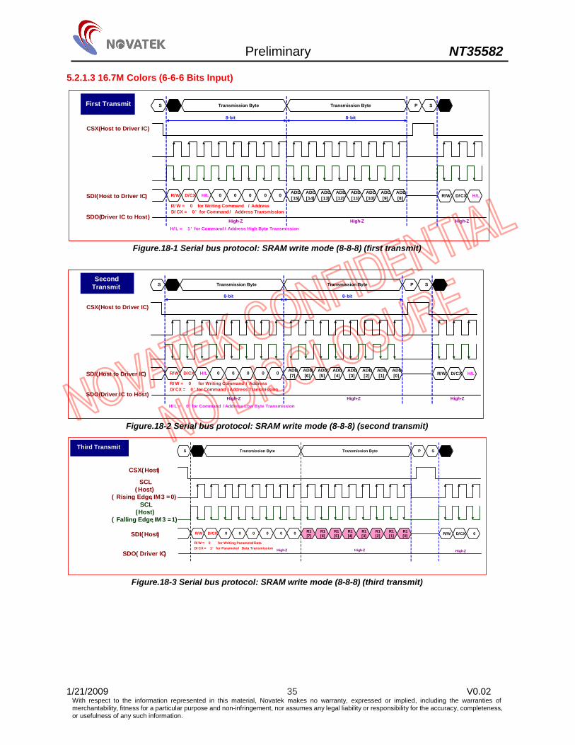
Preliminary NT35582
1/21/2009 35 V0.02 With respect to the information represented in this material, Novatek makes no warranty, expressed or implied, including the warranties of merchantability, fitness for a particular purpose and non-infringement, nor assumes any legal liability or responsibility for the accuracy, completeness, or usefulness of any such information.
5.2.1.3 16.7M Colors (6-6-6 Bits Input)
R/W D/CX H/L 0 0 0 0 0 ADD[15]
ADD[14]
ADD[13]
ADD[12]
ADD[11]
ADD[10]
ADD[9]
ADD[8] R/W D/CX H/L
CSX (Host to Driver IC)
SDI (Host to Driver IC)
SDO (Driver IC to Host)High-Z High-Z High-Z
S P STransmission Byte Transmission ByteFirst Transmit
R/ W = ‘ 0’ for Writing Command / AddressD/ CX = ‘ 0 ' for Command / Address Transmission
8-bit 8-bit
H/ L = ‘ 1 ' for Command / Address High Byte Transmission
Figure.18-1 Serial bus protocol: SRAM write mode (8-8-8) (first transmit)
R/W D/CX H/L 0 0 0 0 0 ADD[7]
ADD[6]
ADD[5]
ADD[4]
ADD[3]
ADD[2]
ADD[1]
ADD[0] R/W D/CX H/L
CSX (Host to Driver IC)
SDI (Host to Driver IC)
SDO (Driver IC to Host)High-Z High-Z High-Z
S P STransmission Byte Transmission ByteSecond
Transmit
R/ W = ‘ 0’ for Writing Command / AddressD/ CX = ‘ 0 ' for Command / Address Transmission
8-bit 8-bit
H/ L = ‘ 0 ' for Command / Address Low Byte Transmission
Figure.18-2 Serial bus protocol: SRAM write mode (8-8-8) (second transmit)
R/W D/CX 0 0 0 0 0 0 R/W D/CX 0
CSX ( Host)
SCL ( Host)
( Rising Edge, IM3 = 0)
SDI ( Host)
SDO ( Driver IC)High-Z High-Z
S P STransmission Byte Transmission Byte
R/ W = ‘ 0’ for Writing Parameter / DataD/ CX = ‘ 1' for Parameter / Data Transmission
SCL (Host)
( Falling Edge, IM 3 = 1)
R1[5]
R1[4]
R1[3]
R1[2]
R1[1]
R1[0]
High-Z
R1[7]
R1[6]
Third Transmit
Figure.18-3 Serial bus protocol: SRAM write mode (8-8-8) (third transmit)

Preliminary NT35582
1/21/2009 36 V0.02 With respect to the information represented in this material, Novatek makes no warranty, expressed or implied, including the warranties of merchantability, fitness for a particular purpose and non-infringement, nor assumes any legal liability or responsibility for the accuracy, completeness, or usefulness of any such information.
R/W D/CX 0 0 0 0 0 0 R/W D/CX 0
CSX ( Host)
SCL ( Host)
( Rising Edge, IM3 = 0)
SDI ( Host)
SDO ( Driver IC) High-Z High-Z
S P STransmission Byte Transmission Byte
R/ W = ‘ 0’ for Writing Parameter / DataD/ CX = ‘ 1' for Parameter / Data Transmission
SCL (Host)
( Falling Edge, IM 3 = 1)
G1[5]
G1[4]
G1[3]
G1[2]
G1[1]
G1[0]
High-Z
G1[7]
G1[6]
Forth Transmit
Figure.18-4 Serial bus protocol: SRAM write mode (8-8-8) (fourth transmit)
R/W D/CX 0 0 0 0 0 0 R/W D/CX 0
CSX ( Host)
SCL ( Host)
( Rising Edge, IM3 = 0)
SDI ( Host)
SDO ( Driver IC) High-Z High-Z
S P STransmission Byte Transmission Byte
R/ W = ‘ 0’ for Writing Parameter / DataD/ CX = ‘ 1 ' for Parameter / Data Transmission
SCL (Host)
( Falling Edge, IM 3 = 1)B1[5]
B1[4]
B1[3]
B1[2]
B1[1]
B1[0]
High-Z
B1[7]
B1[6]
Fifth Transmit
Figure.18-5 Serial bus protocol: SRAM write mode (8-8-8) (fifth transmit)
R/W D/CX 0 0 0 0 0 0 R/W D/CX 0
CSX ( Host)
SCL ( Host)
( Rising Edge, IM3 = 0)
SDI ( Host)
SDO ( Driver IC) High-Z High-Z
S P STransmission Byte Transmission Byte
R/ W = ‘ 0’ for Writing Parameter / DataD/ CX = ‘ 1' for Parameter / Data Transmission
SCL (Host)
( Falling Edge, IM 3 = 1)
High-Z
R2[5]
R2[4]
R2[3]
R2[2]
R2[1]
R2[0]
R2[7]
R2[6]
Sixth Transmit
Figure.18-6 Serial bus protocol: SRAM write mode (8-8-8) (sixth transmit)

Preliminary NT35582
1/21/2009 37 V0.02 With respect to the information represented in this material, Novatek makes no warranty, expressed or implied, including the warranties of merchantability, fitness for a particular purpose and non-infringement, nor assumes any legal liability or responsibility for the accuracy, completeness, or usefulness of any such information.
5.2.2 8-Bit Parallel Interface for Data RAM Write Different display data formats are available for four colors depth supported by the NT35582 listed below. -65k colors, RGB 5,6,5-bits input. -262k colors, RGB 6,6,6-bits input. -16.7M colors, RGB 8,8,8-bits input.
Table 5.2.1 8-Bits Parallel Interface Set Table D23 D22 D21 D20 D19 D18 D17 D16 D15 D14 D13 D12 D11 D10 D9 D8 D7 D6 D5 D4 D3 D2 D1 D0 Register
x x x x x x x x x x x x x x x x 0 0 0 0 0 0 1 0 Register Command
x x x x x x x x x x x x x x x x 1 1 0 0 0 0 0 0 2C00h
3A00h D23 D22 D21 D20 D19 D18 D17 D16 D15 D14 D13 D12 D11 D10 D9 D8 D7 D6 D5 D4 D3 D2 D1 D0 Color x x x x x x x x x x x x x x x x R4 R3 R2 R1 R0 G5 G4 G3
0005h x x x x x x x x x x x x x x x x G2 G1 G0 B4 B3 B2 B1 B0
65K-Color (1-pixels/
2-transfer) x x x x x x x x x x x x x x x x R5 R4 R3 R2 R1 R0 x x x x x x x x x x x x x x x x x x G5 G4 G3 G2 G1 G0 x x 0006h x x x x x x x x x x x x x x x x B5 B4 B3 B2 B1 B0 x x
262K-Color (1-pixels/
3-transfer) x x x x x x x x x x x x x x x x R7 R6 R5 R4 R3 R2 R1 R0 x x x x x x x x x x x x x x x x G7 G6 G5 G4 G3 G2 G1 G0 0007h x x x x x x x x x x x x x x x x B7 B6 B5 B4 B3 B2 B1 B0
16.7M-Color (1-pixels/
3-transfer)
5.2.2.1 65K Colors (5-6-5 Bits Input)
1st write 1 R14 R13 R12 R11 R10 G15 G14 G13 -
2nd write 1 G12 G11 G10 B14 B13 B12 B11 B10 1st pixel data write (R1/G1/B1)
3rd write 1 R24 R23 R22 R2 1 R20 G25 G24 G23 -
4th write 1 G22 G21 G20 B2 4 B23 B22 B21 B2 0 2nd pixel data write (R2/G2/B2)
16 bits extension to 24bits
R1 G1 B1 R2 G2 B2 R3 G3 B3
Frame memory
24 bits
R14 R13 R12 R11 R10 R14 R13 R12 G15 G14 G13 G12 G11 G10 G15 G14 B14 B13 B12 B11 B10 B14 B13 B12
R17 R16 R15 R14 R13 R12 R11 R10 G17 G16 G15 G14 G13 G12 G11 G10 B17 B16 B15 B14 B13 B12 B11 B10
65 K color data D/CX D7 D6 D5 D4 D3 D2 D1 D0 Memory writeMEMWR1 0 -Memory write command code_1 (2C h)
MEMWR2 0 -Memory write command code_2 (00 h)
Figure.19 Write 8-bit data for RGB 5-6-5-bits
Note:
2 times transfer is used to transmit 1 pixel data with the 16-bit color depth information. The most significant bits are:Rx4, Gx5 and Bx4. The least significant bits are:Rx0, Gx0 and Bx0.

Preliminary NT35582
1/21/2009 38 V0.02 With respect to the information represented in this material, Novatek makes no warranty, expressed or implied, including the warranties of merchantability, fitness for a particular purpose and non-infringement, nor assumes any legal liability or responsibility for the accuracy, completeness, or usefulness of any such information.
5.2.2.2 262K Colors (6-6-6 Bits Input)
1st write 1 R15 R14 R13 R12 R11 R10 x x -
2nd write 1 G15 G14 G13 G12 G11 G10 x x -
3rd write 1 B15 B14 B23 B12 B11 B10 x x 1st pixel data write (R1/G1/B1)
4th write 1 R25 R24 R23 R22 R21 R20 x x -
5th write 1 G25 G24 G23 G22 G21 G20 x x -
6th write 1 B25 B24 B23 B22 B21 B20 x x 2nd pixel data write (R2/G2/B2)
18 bits extension to 24bits
R1 G1 B1 R2 G2 B2 R3 G3 B3
Frame memory
24 bits
R15 R14 R13 R12 R11 R10 R15 R14 G15 G14 G13 G12 G11 G10 G15 G14 B15 B14 B13 B12 B11 B10 B15 B14
R17 R16 R15 R14 R13 R12 R11 R10 G17 G16 G15 G14 G13 G12 G11 G10 B17 B16 B15 B14 B13 B12 B11 B10
-Memory write command code_2 (00 h)
262 K color data D/CX D7 D6 D5 D4 D3 D2 D1 D0 Memory writeMEMWR1 0 -Memory write command code_1 (2C h)MEMWR2 0
Figure.20 Write 8-bit data for RGB 6-6-6-bits input Note:
3 times transfer is used to transmit 1 pixel data with the 18-bit color depth information. The most significant bits are:Rx5, Gx5 and Bx5. The least significant bits are:Rx0, Gx0 and Bx0.
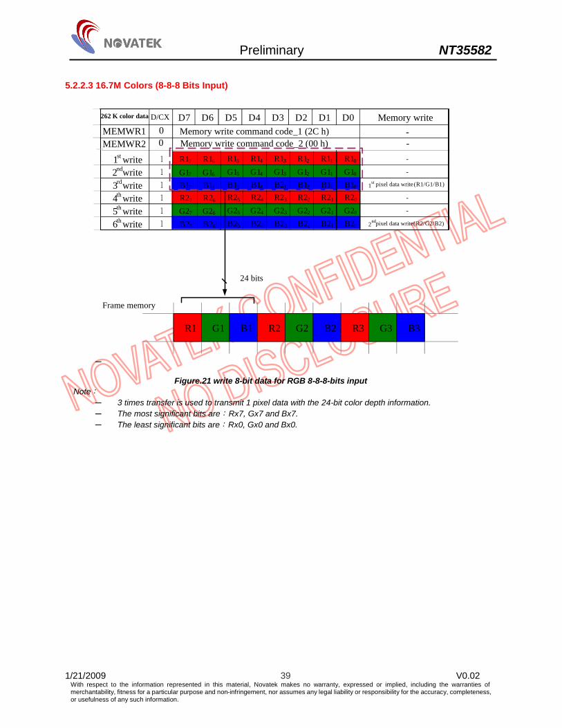
Preliminary NT35582
1/21/2009 39 V0.02 With respect to the information represented in this material, Novatek makes no warranty, expressed or implied, including the warranties of merchantability, fitness for a particular purpose and non-infringement, nor assumes any legal liability or responsibility for the accuracy, completeness, or usefulness of any such information.
5.2.2.3 16.7M Colors (8-8-8 Bits Input)
1st write 1 R15 R14 R13 R12 R11 R10 -
2nd write 1 G15 G14 G13 G12 G11 G10 -
3rd write 1 B15 B14 B23 B12 B11 B10 1st pixel data write (R1/G1/B1)
4th write 1 R25 R24 R23 R22 R21 R20 -
5th write 1 G25 G24 G23 G22 G21 G20 -
6th write 1 B25 B24 B23 B22 B21 B20 2nd pixel data write (R2/G2/B2)
-Memory write command code_2 (00 h)
262 K color data D/CX D7 D6 D5 D4 D3 D2 D1 D0 Memory writeMEMWR1 0 -Memory write command code_1 (2C h)MEMWR2 0
R1 G1 B1 R2 G2 B2 R3 G3 B3
Frame memory
24 bits
R17 R16
G17 G16
B17 B16
R27 R26
G27 G26
B27 B26
Figure.21 write 8-bit data for RGB 8-8-8-bits input
Note: 3 times transfer is used to transmit 1 pixel data with the 24-bit color depth information. The most significant bits are:Rx7, Gx7 and Bx7. The least significant bits are:Rx0, Gx0 and Bx0.

Preliminary NT35582
1/21/2009 40 V0.02 With respect to the information represented in this material, Novatek makes no warranty, expressed or implied, including the warranties of merchantability, fitness for a particular purpose and non-infringement, nor assumes any legal liability or responsibility for the accuracy, completeness, or usefulness of any such information.
5.2.3 16-Bit Parallel Interface for Data RAM Write Different display data formats are available for four colors depth supported by listed below. -65k colors, RGB 5,6,5-bits input. -262k colors, RGB 6,6,6-bits input. -16.7M colors, RGB 8,8,8-bits input.
Table 5.2.2 16-Bits Parallel Interface Set Table D23 D22 D21 D20 D19 D18 D17 D16 D15 D14 D13 D12 D11 D10 D9 D8 D7 D6 D5 D4 D3 D2 D1 D0 Register Register
Command x x x x x x x x 0 0 0 0 0 0 1 0 1 1 0 0 0 0 0 0 2C00h 3A00h D23 D22 D21 D20 D19 D18 D17 D16 D15 D14 D13 D12 D11 D10 D9 D8 D7 D6 D5 D4 D3 D2 D1 D0 Color 0005h x x x x x x x x R4 R3 R2 R1 R0 G5 G4 G3 G2 G1 G0 B4 B3 B2 B1 B0 65K-Color
x x x x x x x x R5 R4 R3 R2 R1 R0 x x G5 G4 G3 G2 G1 G0 x x x x x x x x x x B5 B4 B3 B2 B1 B0 x x R5 R4 R3 R2 R1 R0 x x 0006h x x x x x x x x G5 G4 G3 G2 G1 G0 x x B5 B4 B3 B2 B1 B0 x x
262K-Color (2-pixels/
3-transfer) x x x x x x x x R7 R6 R5 R4 R3 R2 R1 R0 G7 G6 G5 G4 G3 G2 G1 G0 x x x x x x x x B7 B6 B5 B4 B3 B2 B1 B0 R7 R6 R5 R4 R3 R2 R1 R0 0007h x x x x x x x x G7 G6 G5 G4 G3 G2 G1 G0 B7 B6 B5 B4 B3 B2 B1 B0
16.7M-Color (2-pixels/
3-transfer)
5.2.3.1 65K Colors (5-6-5 Bits Input)
65K color data D/CX D15 D14 D13 D12 D11 D10 D9 D8 D7 D6 D5 D4 D3 D2 D1 D0 Memory write
MEMWR 0
1st write 1 R14 R13 R12 R11 R10 G15 G14 G13 G12 G11 G10 B14 B13 B12 B11 B10 1st pixel data write (R1/G1/B1)
2nd write 1 R24 R23 R22 R21 R20 G25 G24 G23 G22 G21 G20 B24 B23 B22 B21 B20 2nd pixel data write (R2/G2/B2)
Memory write command code
16 bits extension to 24bits
R1 G1 B1 R2 G2 B2 R3 G3 B3
Frame memory
24 bits
R14 R13 R12 R11 R10 R14 R13 R12 G15 G14 G13 G12 G11 G10 G15 G14 B14 B13 B12 B11 B10 B14 B13 B12
R17 R16 R15 R14 R13 R12 R11 R10 G17 G16 G15 G14 G13 G12 G11 G10 B17 B16 B15 B14 B13 B12 B11 B10
-
Figure.22 Write 16-bit data for RGB 5-6-5-bits input
Note:
In one transfer (D15 to D0), 1 pixel data is transmitted with the 16-bit color depth information. The most significant bits are:Rx4, Gx5 and Bx4. The least significant bits are:Rx0, Gx0 and Bx0.

Preliminary NT35582
1/21/2009 41 V0.02 With respect to the information represented in this material, Novatek makes no warranty, expressed or implied, including the warranties of merchantability, fitness for a particular purpose and non-infringement, nor assumes any legal liability or responsibility for the accuracy, completeness, or usefulness of any such information.
5.2.3.2 262K Colors (6-6-6 Bits Input)
262K color data D/CX D15 D14 D13 D12 D11 D10 D9 D8 D7 D6 D5 D4 D3 D2 D1 D0 Memory write
MEMWR 0 -1st write 1 R15 R14 R13 R12 R11 R10 x x G15 G14 G13 G12 G11 G10 x x -
2nd write 1 B15 B14 B13 B12 B11 B10 x x R25 R24 R23 R22 R21 R20 x x 1st pixel data write (R1/G1/B1)
3rd write 1 G25 G24 G23 G22 G21 G20 x x B25 B24 B23 B22 B21 B20 x x 2nd pixel data write (R2/G2/B2)
Memory write command code
18 bits extension to 24bits
R1 G1 B1 R2 G2 B2 R3 G3 B3
Frame memory
24 bits
R15 R14 R13 R12 R11 R10 R15 R14 G15 G14 G13 G12 G11 G10 G15 G14 B15 B14 B13 B12 B11 B10 B15 B14
R17 R16 R15 R14 R13 R12 R11 R10 G17 G16 G15 G14 G13 G12 G11 G10 B17 B16 B15 B14 B13 B12 B11 B10
Figure.23 Write 16-bit data for RGB 6-6-6-bits input
Note:
3 times transfer is used to transmit 2 pixels data or 2 times transfer are used to transmit 1 pixel data with the 18-bit color depth information..
The most significant bits are:Rx5, Gx5 and Bx5. The least significant bits are:Rx0, Gx0 and Bx0.

Preliminary NT35582
1/21/2009 42 V0.02 With respect to the information represented in this material, Novatek makes no warranty, expressed or implied, including the warranties of merchantability, fitness for a particular purpose and non-infringement, nor assumes any legal liability or responsibility for the accuracy, completeness, or usefulness of any such information.
5.2.3.3 16.7M Colors (8-8-8 Bits Input)
262K color data D/CX D15 D14 D13 D12 D11 D10 D9 D8 D7 D6 D5 D4 D3 D2 D1 D0 Memory write
MEMWR 0 -1st write 1 R17 R16 R15 R14 R13 R12 G17 G16 G15 G14 G13 G12 -
2nd write 1 B17 B16 B15 B14 B13 B12 R27 R26 R25 R24 R23 R22 1st pixel data write (R1/G1/B1)
3rd write 1 G27 G26 G25 G24 G23 G22 B27 B26 B25 B24 B23 B22 2nd pixel data write (R2/G2/B2)
Memory write command code
R1 G1 B1 R2 G2 B2 R3 G3 B3
Frame memory
24 bits
R11 R10
B11 B10
G21 G20
G11 G10
R21 R20
B21 B20
Figure.24 Write 16-bit data for RGB 8-8-8-bits input
Note:
3 times transfer is used to transmit 2 pixels data or 2 times transfer are used to transmit 1 pixel data with the 24-bit color depth information..
The most significant bits are:Rx7, Gx7 and Bx7. The least significant bits are:Rx0, Gx0 and Bx0.

Preliminary NT35582
1/21/2009 43 V0.02 With respect to the information represented in this material, Novatek makes no warranty, expressed or implied, including the warranties of merchantability, fitness for a particular purpose and non-infringement, nor assumes any legal liability or responsibility for the accuracy, completeness, or usefulness of any such information.
5.2.4 24-Bit Parallel Interface for Data RAM Write Different display data formats are available for four colors depth supported by listed below. -65k colors, RGB 5,6,5-bits input -262k colors, RGB 6,6,6-bits input -16.7M colors, RGB 8,8,8-bits input
Table 5.2.3 24-Bits Parallel Interface Set Table D23 D22 D21 D20 D19 D18 D17 D16 D15 D14 D13 D12 D11 D10 D9 D8 D7 D6 D5 D4 D3 D2 D1 D0 Register Register
Command x x x x x x x x 0 0 0 0 0 0 1 0 1 1 0 0 0 0 0 0 2C00h 3A00h D23 D22 D21 D20 D19 D18 D17 D16 D15 D14 D13 D12 D11 D10 D9 D8 D7 D6 D5 D4 D3 D2 D1 D0 Color 0005h x x x x x x x x R4 R3 R2 R1 R0 G5 G4 G3 G2 G1 G0 B4 B3 B2 B1 B0 65K-Color 0006h x x x x x x R5 R4 R3 R2 R1 R0 G5 G4 G3 G2 G1 G0 B5 B4 B3 B2 B1 B0 262K-Color 0007h R7 R6 R5 R4 R3 R2 R1 R0 G7 G6 G5 G4 G3 G2 G1 G0 B7 B6 B5 B4 B3 B2 B1 B0 16.7M-Color
5.2.4.1 65K Colors (5-6-5 Bits Input)
16 bits extension to 24bits
R1 G1 B1 R2 G2 B2 R3 G3 B3
Frame memory
24 bits
R14 R13 R12 R11 R10 R14 R13 R12 G15 G14 G13 G12 G11 G10 G15 G14 B14 B13 B12 B11 B10 B14 B13 B12
R17 R16 R15 R14 R13 R12 R11 R10 G17 G16 G15 G14 G13 G12 G11 G10 B17 B16 B15 B14 B13 B12 B11 B10
2nd pixel data write (R2/G2/B2)
B20
B21
B22
B23
B24
G20
G21
G22
G23
G24
G25
R20
R21
R22
R23
R24
xxxxxxxx12nd write
1st pixel data write (R1/G1/B1)
B10
B11
B12
B13
B14
G10
G11
G12
G13
G14
G15
R10
R11
R12
R13
R14
xxxxxxxx11st write
-Memory write command codex0MEMWR
Memory writeD0
D1
D2
D3
D4
D5
D6
D7
D8
D9
D10
D11
D12
D13
D14
D15
D16
D17
D18
D19
D20
D21
D22
D23
D/CX
65 K color data
Figure.25 Write 24-bit data for RGB 5-6-5-bits input
Note: In one transfer (D15 to D0), 1 pixel data is transmitted with the 16-bit color depth information. The most significant bits are:Rx4, Gx5 and Bx4. The least significant bits are:Rx0, Gx0 and Bx0.
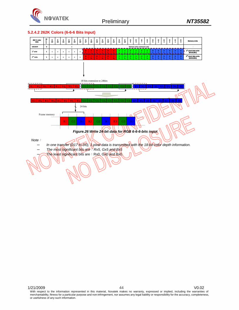
Preliminary NT35582
1/21/2009 44 V0.02 With respect to the information represented in this material, Novatek makes no warranty, expressed or implied, including the warranties of merchantability, fitness for a particular purpose and non-infringement, nor assumes any legal liability or responsibility for the accuracy, completeness, or usefulness of any such information.
5.2.4.2 262K Colors (6-6-6 Bits Input)
18 bits extension to 24bits
R1 G1 B1 R2 G2 B2 R3 G3 B3
Frame memory
24 bits
R15 R14 R13 R12 R11 R10 R15 R14 G15 G14 G13 G12 G11 G10 G15 G14 B15 B14 B13 B12 B11 B10 B15 B14
R17 R16 R15 R14 R13 R12 R11 R10 G17 G16 G15 G14 G13 G12 G11 G10 B17 B16 B15 B14 B13 B12 B11 B10
2nd pixel data write (R2/G2/B2)
B20
B21
B22
B23
B24
B25
G20
G21
G22
G23
G24
G25
R20
R21
R22
R23
R24
R25
xxxxxx12nd write
1st pixel data write (R1/G1/B1)
B10
B11
B12
B13
B14
B15
G10
G11
G12
G13
G14
G15
R10
R11
R12
R13
R14
R15
xxxxxx11st write
-Memory write command codex0MEMWR
Memory writeD0
D1
D2
D3
D4
D5
D6
D7
D8
D9
D10
D11
D12
D13
D14
D15
D16
D17
D18
D19
D20
D21
D22
D23
D/CX
262 K color data
Figure.26 Write 24-bit data for RGB 6-6-6-bits input
Note:
In one transfer (D17 to D0), 1 pixel data is transmitted with the 18-bit color depth information. The most significant bits are:Rx5, Gx5 and Bx5 The least significant bits are:Rx0, Gx0 and Bx0.

Preliminary NT35582
1/21/2009 45 V0.02 With respect to the information represented in this material, Novatek makes no warranty, expressed or implied, including the warranties of merchantability, fitness for a particular purpose and non-infringement, nor assumes any legal liability or responsibility for the accuracy, completeness, or usefulness of any such information.
5.2.4.3 16.7M Colors (8-8-8 Bits Input)
R1 G1 B1 R2 G2 B2 R3 G3 B3
Frame memory
24 bits
2nd pixel data write (R2/G2/B2)
B20
B21
B22
B23
B24
B25
B26
B27
G20
G21
G22
G23
G24
G25
G26
G27
R20
R21
R22
R23
R24
R25
R26
R27
12nd write
1st pixel data write (R1/G1/B1)
B10
B11
B12
B13
B14
B15
B16
B17
G10
G11
G12
G13
G14
G15
G16
G17
R10
R11
R12
R13
R14
R15
R16
R17
11st write
-Memory write command codex0MEMWR
Memory writeD0
D1
D2
D3
D4
D5
D6
D7
D8
D9
D10
D11
D12
D13
D14
D15
D16
D17
D18
D19
D20
D21
D22
D23
D/CX
16.7 M color data
Figure.27 Write 24-bit data for RGB 8-8-8-bits
Note:
In one transfer (D23 to D0), 1 pixel data is transmitted with the 24-bit color depth information. The most significant bits are:Rx7, Gx7 and Bx7 The least significant bits are:Rx0, Gx0 and Bx0.
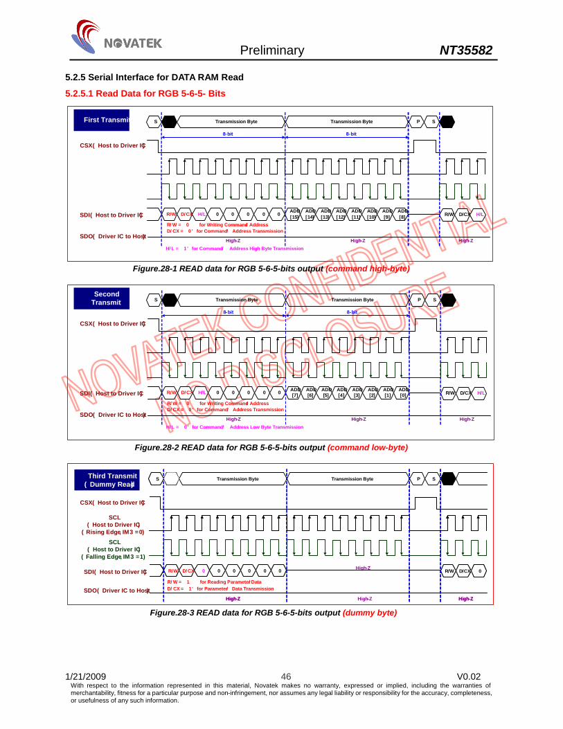
Preliminary NT35582
1/21/2009 46 V0.02 With respect to the information represented in this material, Novatek makes no warranty, expressed or implied, including the warranties of merchantability, fitness for a particular purpose and non-infringement, nor assumes any legal liability or responsibility for the accuracy, completeness, or usefulness of any such information.
5.2.5 Serial Interface for DATA RAM Read
5.2.5.1 Read Data for RGB 5-6-5- Bits
R/W D/CX H/L 0 0 0 0 0 ADD[15]
ADD[14]
ADD[13]
ADD[12]
ADD[11]
ADD[10]
ADD[9]
ADD[8] R/W D/CX H/L
CSX ( Host to Driver IC)
SDI ( Host to Driver IC)
SDO ( Driver IC to Host)High-Z High-Z High-Z
S P STransmission Byte Transmission ByteFirst Transmit
R/ W = ‘ 0’ for Writing Command / AddressD/ CX = ‘ 0 ' for Command / Address Transmission
8-bit 8-bit
H/ L = ‘ 1 ' for Command / Address High Byte Transmission
Figure.28-1 READ data for RGB 5-6-5-bits output (command high-byte)
R/W D/CX H/L 0 0 0 0 0 ADD[7]
ADD[6]
ADD[5]
ADD[4]
ADD[3]
ADD[2]
ADD[1]
ADD[0] R/W D/CX H/L
CSX ( Host to Driver IC)
SDI ( Host to Driver IC)
SDO ( Driver IC to Host)High-Z High-Z High-Z
S P STransmission Byte Transmission ByteSecond
Transmit
R/ W = ‘ 0’ for Writing Command / AddressD/ CX = ‘ 0 ' for Command / Address Transmission
8-bit 8-bit
H/ L = ‘ 0 ' for Command / Address Low Byte Transmission
Figure.28-2 READ data for RGB 5-6-5-bits output (command low-byte)
R/W D/CX 0 0 0 0 0 0 R/W D/CX 0
High-Z High-Z
S P STransmission Byte Transmission Byte
R/ W = ‘ 1’ for Reading Parameter / DataD/ CX = ‘ 1' for Parameter / Data Transmission
High-Z
High-Z
CSX ( Host to Driver IC)
SCL ( Host to Driver IC)
( Rising Edge, IM3 = 0)
SDI ( Host to Driver IC)
SDO ( Driver IC to Host)
SCL ( Host to Driver IC)
( Falling Edge, IM3 = 1)
Third Transmit( Dummy Read)
R/W D/CX 0 0 0 0 0 0 R/W D/CX 0
High-Z High-Z
S
Figure.28-3 READ data for RGB 5-6-5-bits output (dummy byte)

Preliminary NT35582
1/21/2009 47 V0.02 With respect to the information represented in this material, Novatek makes no warranty, expressed or implied, including the warranties of merchantability, fitness for a particular purpose and non-infringement, nor assumes any legal liability or responsibility for the accuracy, completeness, or usefulness of any such information.
R/W D/CX 0 0 0 0 0 0 R/W D/CX 0
High-Z High-Z
S P STransmission Byte Transmission Byte
R/ W = ‘ 1’ for Reading Parameter / DataD/ CX = ‘ 1' for Parameter / Data Transmission
High-Z
R1[4]
R1[3]
R1[2]
R1[1]
R1[0]
CSX ( Host to Driver IC)
SCL ( Host to Driver IC)
( Rising Edge, IM 3 = 0)
SDI ( Host to Driver IC)
SDO ( Driver IC to Host)
SCL ( Host to Driver IC)
( Falling Edge, IM 3 = 1)
Forth Transmit
xxx
Figure.28-4 READ data for RGB 5-6-5-bits output (data R1[4:0])
R/W D/CX 0 0 0 0 0 0 R/W D/CX 0
High-Z High-Z
S P STransmission Byte Transmission Byte
R/ W = ‘ 1’ for Reading Parameter / DataD/ CX = ‘ 1' for Parameter / Data Transmission
High-Z
G1[5]
G1[4]
G1[3]
G1[2]
G1[1]
G1[0]
CSX ( Host to Driver IC)
SCL ( Host to Driver IC)
( Rising Edge, IM3 = 0)
SDI ( Host to Driver IC)
SDO ( Driver IC to Host)
SCL ( Host to Driver IC)
( Falling Edge, IM3 = 1)
Fifth Transmit
xx
Figure.28-5 READ data for RGB 5-6-5-bits output (data G1[5:0])
R/W D/CX 0 0 0 0 0 0 R/W D/CX 0
High-Z High-Z
S P STransmission Byte Transmission Byte
R/ W = ‘ 1’ for Reading Parameter / DataD/ CX = ‘ 1 ' for Parameter / Data Transmission
High-Z
B1[4]
B1[3]
B1[2]
B1[1]
B1[0]
CSX ( Host to Driver IC)
SCL ( Host to Driver IC)
( Rising Edge, IM3 = 0)
SDI ( Host to Driver IC)
SDO ( Driver IC to Host)
SCL ( Host to Driver IC)
( Falling Edge, IM3 = 1)
Sixth Transmit
xxx
Figure.28-6 READ data for RGB 5-6-5-bits output (data B1[4:0])
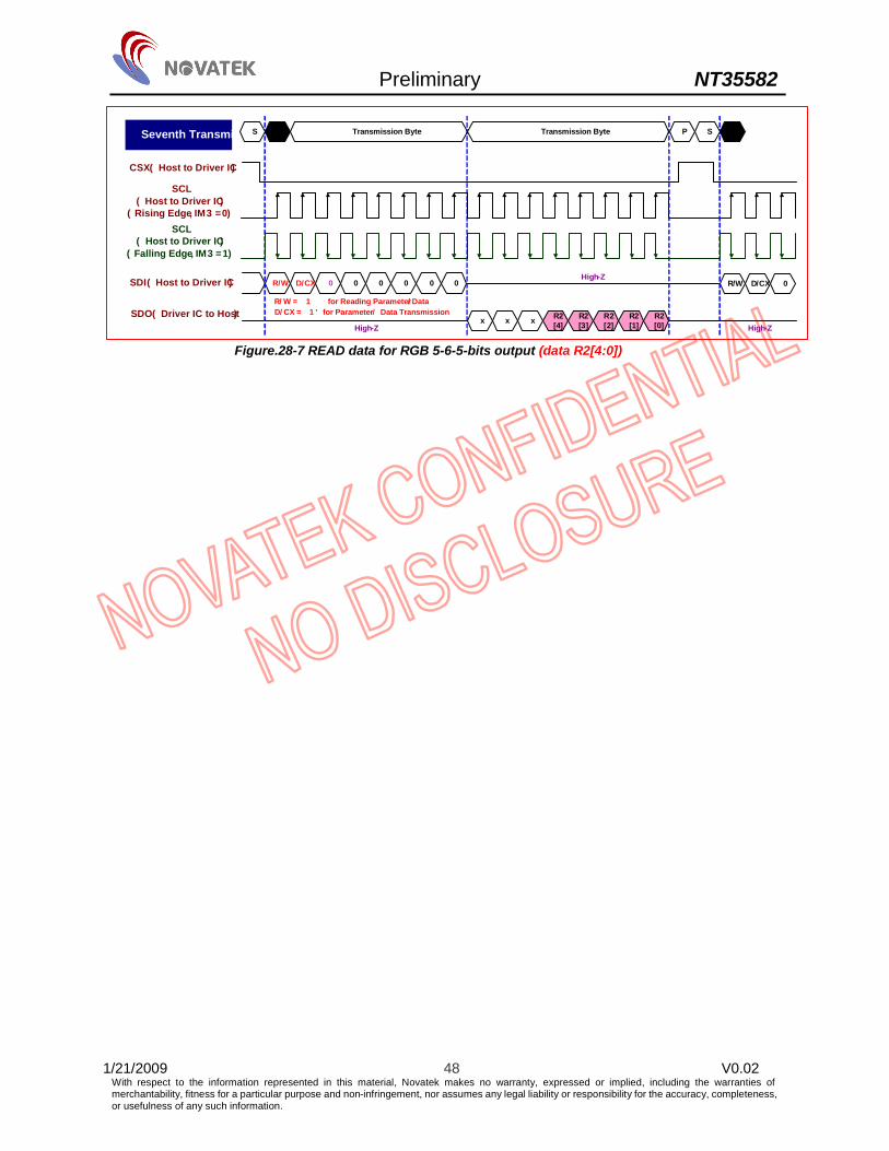
Preliminary NT35582
1/21/2009 48 V0.02 With respect to the information represented in this material, Novatek makes no warranty, expressed or implied, including the warranties of merchantability, fitness for a particular purpose and non-infringement, nor assumes any legal liability or responsibility for the accuracy, completeness, or usefulness of any such information.
R/W D/CX 0 0 0 0 0 0 R/W D/CX 0
High-Z High-Z
S P STransmission Byte Transmission Byte
R/ W = ‘ 1’ for Reading Parameter / DataD/ CX = ‘ 1 ' for Parameter / Data Transmission
High-Z
R2[4]
R2[3]
R2[2]
R2[1]
R2[0]
CSX ( Host to Driver IC)
SCL ( Host to Driver IC)
( Rising Edge, IM3 = 0)
SDI ( Host to Driver IC)
SDO ( Driver IC to Host)
SCL ( Host to Driver IC)
( Falling Edge, IM3 = 1)
Seventh Transmit
xxx
Figure.28-7 READ data for RGB 5-6-5-bits output (data R2[4:0])
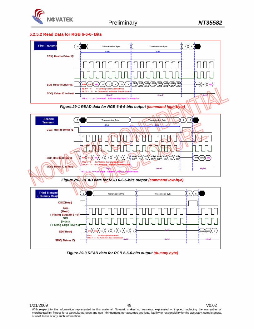
Preliminary NT35582
1/21/2009 49 V0.02 With respect to the information represented in this material, Novatek makes no warranty, expressed or implied, including the warranties of merchantability, fitness for a particular purpose and non-infringement, nor assumes any legal liability or responsibility for the accuracy, completeness, or usefulness of any such information.
5.2.5.2 Read Data for RGB 6-6-6- Bits
R/W D/CX H/L 0 0 0 0 0 ADD[15]
ADD[14]
ADD[13]
ADD[12]
ADD[11]
ADD[10]
ADD[9]
ADD[8] R/W D/CX H/L
CSX ( Host to Driver IC)
SDI ( Host to Driver IC)
SDO ( Driver IC to Host)High-Z High-Z High-Z
S P STransmission Byte Transmission ByteFirst Transmit
R/ W = ‘ 0’ for Writing Command / AddressD/ CX = ‘ 0 ' for Command / Address Transmission
8-bit 8-bit
H/ L = ‘ 1 ' for Command / Address High Byte Transmission
Figure.29-1 READ data for RGB 6-6-6-bits output (command high-byte)
R/W D/CX H/L 0 0 0 0 0 ADD[7]
ADD[6]
ADD[5]
ADD[4]
ADD[3]
ADD[2]
ADD[1]
ADD[0] R/W D/CX H/L
CSX ( Host to Driver IC)
SDI ( Host to Driver IC)
SDO ( Driver IC to Host)High-Z High-Z High-Z
S P STransmission Byte Transmission ByteSecond Transmit
R/ W = ‘ 0’ for Writing Command / AddressD/ CX = ‘ 0 ' for Command / Address Transmission
8-bit 8-bit
H/ L = ‘ 0 ' for Command / Address Low Byte Transmission
Figure.29-2 READ data for RGB 6-6-6-bits output (command low-bye)
R/W D/CX 0 0 0 0 0 0 R/W D/CX 0
CSX (Host)
SCL (Host)
( Rising Edge, IM 3 = 0)
SDI ( Host)
SDO ( Driver IC) High-Z High-Z
S P STransmission Byte Transmission Byte
R/ W = ‘ 1 ’ for Reading Parameter / DataD/ CX = ‘ 1 ' for Parameter / Data Transmission
SCL ( Host)
( Falling Edge, IM3 = 1)High-Z
High-Z
Third Transmit( Dummy Read)
Figure.29-3 READ data for RGB 6-6-6-bits output (dummy byte)

Preliminary NT35582
1/21/2009 50 V0.02 With respect to the information represented in this material, Novatek makes no warranty, expressed or implied, including the warranties of merchantability, fitness for a particular purpose and non-infringement, nor assumes any legal liability or responsibility for the accuracy, completeness, or usefulness of any such information.
R/W D/CX 0 0 0 0 0 0 R/W D/CX 0
CSX (Host)
SCL (Host)
( Rising Edge, IM 3 = 0)
SDI (Host)
SDO ( Driver IC) High-Z High-Z
S P STransmission Byte Transmission Byte
R/ W = ‘ 1 ’ for Reading Parameter / DataD/ CX = ‘ 1 ' for Parameter / Data Transmission
SCL ( Host)
( Falling Edge, IM3 = 1)High-Z
0 0 R1[5]
R1[4]
R1[3]
R1[2]
R1[1]
R1[0]
Forth Transmit
Figure.29-4 READ data for RGB 6-6-6-bits output (data R1[5:0])
R/W D/CX 0 0 0 0 0 0 R/W D/CX 0
CSX (Host)
SCL (Host)
( Rising Edge, IM3 = 0)
SDI (Host)
SDO ( Driver IC) High-Z High-Z
S P STransmission Byte Transmission Byte
R/ W = ‘ 1 ’ for Reading Parameter / DataD/ CX = ‘ 1 ' for Parameter / Data Transmission
SCL ( Host)
( Falling Edge, IM3 = 1)High-Z
0 0 G1[5]
G1[4]
G1[3]
G1[2]
G1[1]
G1[0]
Fifth Transmit
Figure.29-5 READ data for RGB 6-6-6-bits output (data G1[5:0])
R/W D/CX 0 0 0 0 0 0 R/W D/CX 0
CSX (Host)
SCL (Host)
( Rising Edge, IM3 = 0)
SDI (Host)
SDO ( Driver IC) High-Z High-Z
S P STransmission Byte Transmission Byte
R/ W = ‘ 1 ’ for Reading Parameter / DataD/ CX = ‘ 1 ' for Parameter / Data Transmission
SCL ( Host)
( Falling Edge, IM3 = 1)High-Z
0 0 B1[5]
B1[4]
B1[3]
B1[2]
B1[1]
B1[0]
Sixth Transmit
Figure.29-6 READ data for RGB 6-6-6-bits output (data B1[5:0])
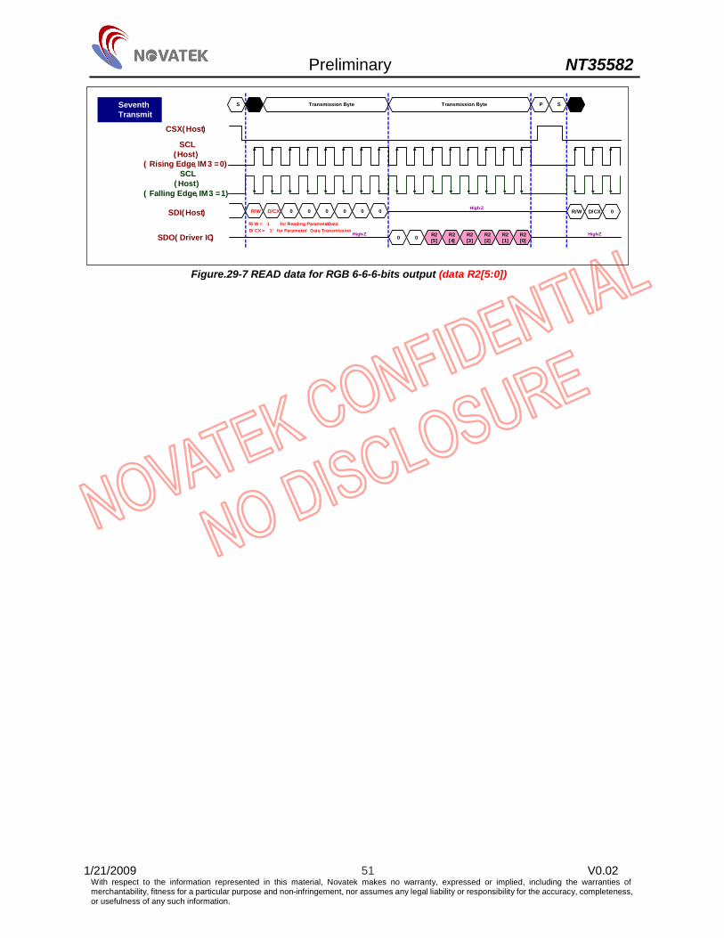
Preliminary NT35582
1/21/2009 51 V0.02 With respect to the information represented in this material, Novatek makes no warranty, expressed or implied, including the warranties of merchantability, fitness for a particular purpose and non-infringement, nor assumes any legal liability or responsibility for the accuracy, completeness, or usefulness of any such information.
R/W D/CX 0 0 0 0 0 0 R/W D/CX 0
CSX (Host)
SCL (Host)
( Rising Edge, IM 3 = 0)
SDI ( Host)
SDO ( Driver IC) High-Z High-Z
S P STransmission Byte Transmission Byte
R/ W = ‘ 1 ’ for Reading Parameter / DataD/ CX = ‘ 1 ' for Parameter / Data Transmission
SCL ( Host)
( Falling Edge, IM3 = 1)High-Z
0 0 R2[5]
R2[4]
R2[3]
R2[2]
R2[1]
R2[0]
Seventh Transmit
Figure.29-7 READ data for RGB 6-6-6-bits output (data R2[5:0])

Preliminary NT35582
1/21/2009 52 V0.02 With respect to the information represented in this material, Novatek makes no warranty, expressed or implied, including the warranties of merchantability, fitness for a particular purpose and non-infringement, nor assumes any legal liability or responsibility for the accuracy, completeness, or usefulness of any such information.
5.2.5.3 Read Data for RGB 8-8-8- Bits
R/W D/CX H/L 0 0 0 0 0 ADD[15]
ADD[14]
ADD[13]
ADD[12]
ADD[11]
ADD[10]
ADD[9]
ADD[8] R/W D/CX H/L
CSX ( Host to Driver IC)
SDI ( Host to Driver IC)
SDO ( Driver IC to Host)High-Z High-Z High-Z
S P STransmission Byte Transmission ByteFirst Transmit
R/ W = ‘ 0’ for Writing Command / AddressD/ CX = ‘ 0 ' for Command / Address Transmission
8-bit 8-bit
H/ L = ‘ 1' for Command / Address High Byte Transmission
Figure.30-1 READ data for RGB 8-8-8-bits output (command high-byte)
R/W D/CX H/L 0 0 0 0 0 ADD[7]
ADD[6]
ADD[5]
ADD[4]
ADD[3]
ADD[2]
ADD[1]
ADD[0] R/W D/CX H/L
CSX ( Host to Driver IC)
SDI ( Host to Driver IC)
SDO ( Driver IC to Host)High-Z High-Z High-Z
S P STransmission Byte Transmission ByteSecond
Transmit
R/ W = ‘ 0’ for Writing Command / AddressD/ CX = ‘ 0 ' for Command / Address Transmission
8-bit 8-bit
H/ L = ‘ 0' for Command / Address Low Byte Transmission
Figure.30-2 READ data for RGB 8-8-8-bits output (command low-byte)
R/W D/CX 0 0 0 0 0 0 R/W D/CX 0
High-Z High-Z
S P STransmission Byte Transmission Byte
R/ W = ‘ 1’ for Reading Parameter / DataD/ CX = ‘ 1 ' for Parameter / Data Transmission
High-Z
High-Z
CSX ( Host to Driver IC)
SCL ( Host to Driver IC)
( Rising Edge, IM3 = 0)
SDI ( Host to Driver IC)
SDO ( Driver IC to Host)
SCL ( Host to Driver IC)
( Falling Edge, IM 3 = 1)
Third Transmit( Dummy Read)
Figure.30-3 READ data for RGB 8-8-8-bits output (dummy byte)

Preliminary NT35582
1/21/2009 53 V0.02 With respect to the information represented in this material, Novatek makes no warranty, expressed or implied, including the warranties of merchantability, fitness for a particular purpose and non-infringement, nor assumes any legal liability or responsibility for the accuracy, completeness, or usefulness of any such information.
R/W D/CX 0 0 0 0 0 0 R/W D/ CX 0
High-Z High-Z
S P STransmission Byte Transmission Byte
R/ W = ‘ 1’ for Reading Parameter / DataD/ CX = ‘ 1' for Parameter / Data Transmission
High-Z
R1[4]
R1[3]
R1[2]
R1[1]
R1[0]
CSX ( Host to Driver IC)
SCL ( Host to Driver IC)
( Rising Edge, IM 3 = 0)
SDI ( Host to Driver IC)
SDO ( Driver IC to Host)
SCL ( Host to Driver IC)
( Falling Edge, IM 3 = 1)
Forth Transmit
R1[5]
R1[7]
R1[6]
Figure.30-4 READ data for RGB 8-8-8-bits output (data R1[7:0])
R/W D/CX 0 0 0 0 0 0 R/W D/CX 0
High-Z High-Z
S P STransmission Byte Transmission Byte
R/ W = ‘ 1’ for Reading Parameter / DataD/ CX = ‘ 1 ' for Parameter / Data Transmission
High-Z
G1[5]
G1[4]
G1[3]
G1[2]
G1[1]
G1[0]
CSX ( Host to Driver IC)
SCL ( Host to Driver IC)
( Rising Edge, IM3 = 0)
SDI ( Host to Driver IC)
SDO ( Driver IC to Host)
SCL ( Host to Driver IC)
( Falling Edge, IM3 = 1)
Fifth Transmit
G1[7]
G1[6]
Figure.30-5 READ data for RGB 8-8-8-bits output (data G1[7:0])
R/W D/CX 0 0 0 0 0 0 R/W D/CX 0
High-Z High-Z
S P STransmission Byte Transmission Byte
R/ W = ‘ 1’ for Reading Parameter / DataD/ CX = ‘ 1 ' for Parameter / Data Transmission
High-Z
B1[4]
B1[3]
B1[2]
B1[1]
B1[0]
CSX ( Host to Driver IC)
SCL ( Host to Driver IC)
( Rising Edge, IM3 = 0)
SDI ( Host to Driver IC)
SDO ( Driver IC to Host)
SCL ( Host to Driver IC)
( Falling Edge, IM 3 = 1)
Sixth Transmit
B1[7]
B1[6]
B1[5]
Figure.30-6 READ data for RGB 8-8-8-bits output (data B1[7:0])

Preliminary NT35582
1/21/2009 54 V0.02 With respect to the information represented in this material, Novatek makes no warranty, expressed or implied, including the warranties of merchantability, fitness for a particular purpose and non-infringement, nor assumes any legal liability or responsibility for the accuracy, completeness, or usefulness of any such information.
R/W D/CX 0 0 0 0 0 0 R/W D/CX 0
High-Z High-Z
S P STransmission Byte Transmission Byte
R/ W = ‘ 1’ for Reading Parameter / DataD/ CX = ‘ 1' for Parameter / Data Transmission
High-Z
R2[4]
R2[3]
R2[2]
R2[1]
R2[0]
CSX ( Host to Driver IC)
SCL ( Host to Driver IC)
( Rising Edge, IM 3 = 0)
SDI ( Host to Driver IC)
SDO ( Driver IC to Host)
SCL ( Host to Driver IC)
( Falling Edge, IM3 = 1)
Seventh Transmit
R2[7]
R2[6]
R2[5]
Figure.30-7 READ data for RGB 8-8-8-bits output (data R2[7:0])
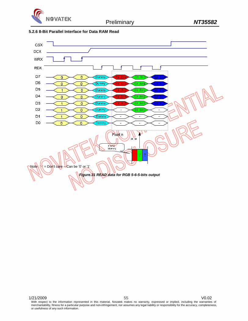
Preliminary NT35582
1/21/2009 55 V0.02 With respect to the information represented in this material, Novatek makes no warranty, expressed or implied, including the warranties of merchantability, fitness for a particular purpose and non-infringement, nor assumes any legal liability or responsibility for the accuracy, completeness, or usefulness of any such information.
5.2.6 8-Bit Parallel Interface for Data RAM Read
Note : ‘-‘ = Don't care – Can be '0' or '1'
Figure.31 READ data for RGB 5-6-5-bits output

Preliminary NT35582
1/21/2009 56 V0.02 With respect to the information represented in this material, Novatek makes no warranty, expressed or implied, including the warranties of merchantability, fitness for a particular purpose and non-infringement, nor assumes any legal liability or responsibility for the accuracy, completeness, or usefulness of any such information.
Note : ‘-‘ = Don't care – Can be '0' or '1'
Figure.32 READ data for RGB 6-6-6-bits output

Preliminary NT35582
1/21/2009 57 V0.02 With respect to the information represented in this material, Novatek makes no warranty, expressed or implied, including the warranties of merchantability, fitness for a particular purpose and non-infringement, nor assumes any legal liability or responsibility for the accuracy, completeness, or usefulness of any such information.
Note : ‘-‘ = Don't care – Can be '0' or '1'
Figure.33 READ data for RGB 8-8-8-bits output
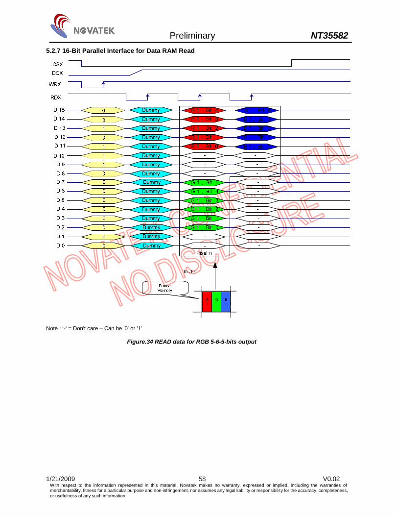
Preliminary NT35582
1/21/2009 58 V0.02 With respect to the information represented in this material, Novatek makes no warranty, expressed or implied, including the warranties of merchantability, fitness for a particular purpose and non-infringement, nor assumes any legal liability or responsibility for the accuracy, completeness, or usefulness of any such information.
5.2.7 16-Bit Parallel Interface for Data RAM Read
Note : ‘-‘ = Don't care – Can be '0' or '1'
Figure.34 READ data for RGB 5-6-5-bits output

Preliminary NT35582
1/21/2009 59 V0.02 With respect to the information represented in this material, Novatek makes no warranty, expressed or implied, including the warranties of merchantability, fitness for a particular purpose and non-infringement, nor assumes any legal liability or responsibility for the accuracy, completeness, or usefulness of any such information.
Note : ‘-‘ = Don't care – Can be '0' or '1'
Figure.35 READ data for RGB 6-6-6-bits output

Preliminary NT35582
1/21/2009 60 V0.02 With respect to the information represented in this material, Novatek makes no warranty, expressed or implied, including the warranties of merchantability, fitness for a particular purpose and non-infringement, nor assumes any legal liability or responsibility for the accuracy, completeness, or usefulness of any such information.
0
0
0
0
0
0
0
0
D 7
D 6
D 5
D 4
D 3
D 2
D 1
D 0
D 15
D 14
D 13
D 12
D 11
D 10
D 9
D 8
24 bit
FrameMemory
B1
R1
G1
CSX
DCX
WRX
RDX
0
1
1
1
0
10
0
Pixel n
G 1 , Bit 3
G 1 , Bit 2
G 1 , Bit 1
G 1 , Bit 0
G 1 , Bit 5
G 1 , Bit 4
B 1 , Bit 3
B 1 , Bit 2
B 1 , Bit 1
B 1 , Bit 0
B 1 , Bit 4
R 1 , Bit 3
R 1 , Bit 2
R 1 , Bit 1
R 1 , Bit 0
R 1 , Bit 4
R 1 , Bit 5 B 1 , Bit 5
Dummy
Dummy
Dummy
Dummy
Dummy
Dummy
Dummy
DummyDummy
Dummy
Dummy
Dummy
Dummy
Dummy
Dummy
Dummy
R 1 , Bit 6
R 1 , Bit 7
G 1 , Bit 7
G 1 , Bit 6
B 1 , Bit 6
B 1 , Bit 7
Note : ‘-‘ = Don't care – Can be '0' or '1'
Figure.36 READ data for RGB 8-8-8-bits output

Preliminary NT35582
1/21/2009 61 V0.02 With respect to the information represented in this material, Novatek makes no warranty, expressed or implied, including the warranties of merchantability, fitness for a particular purpose and non-infringement, nor assumes any legal liability or responsibility for the accuracy, completeness, or usefulness of any such information.
5.2.8 24-Bit Parallel Interface for Data RAM Read
Note : ‘-‘ = Don't care – Can be '0' or '1'
Figure.37 READ data for RGB 5-6-5-bits output

Preliminary NT35582
1/21/2009 62 V0.02 With respect to the information represented in this material, Novatek makes no warranty, expressed or implied, including the warranties of merchantability, fitness for a particular purpose and non-infringement, nor assumes any legal liability or responsibility for the accuracy, completeness, or usefulness of any such information.
: : :
0
0
0
0
D 10
D9
D8D7
D2
D1D0
Pixel n
D 20D 19
D 18D 17D 16
D 15
D 11 G 1 , Bit 1
G 1 , Bit 0
B1 , Bit 0
R1 , Bit 1
R1 , Bit 0
18 bit
FrameMemory
B1
R1
G1
R1 , Bit 2
G1 , Bit 5
B1 , Bit 5
CSX
DCX
WRX
RDX
D 23 R1 , Bit 5
: : :
: : :
0
111
0
:
:
:
Dummy
Dummy
Dummy
Dummy
Dummy
Dummy
Dummy
DummyDummy
Dummy
Dummy
Dummy
Dummy
Dummy
Dummy
Note : ‘-‘ = Don't care – Can be '0' or '1'
Figure.38 READ data for RGB 6-6-6-bits output
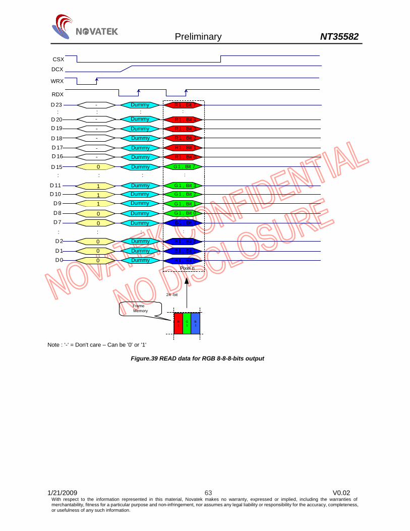
Preliminary NT35582
1/21/2009 63 V0.02 With respect to the information represented in this material, Novatek makes no warranty, expressed or implied, including the warranties of merchantability, fitness for a particular purpose and non-infringement, nor assumes any legal liability or responsibility for the accuracy, completeness, or usefulness of any such information.
: : :
0
0
0
0
D 10
D9
D8D7
D2
D1D0
Pixel n
D 20D 19
D 18D 17D 16
D 15
D 11 G 1 , Bit 3
G 1 , Bit 2
G 1 , Bit 1
G 1 , Bit 0
B1 , Bit 2
B1 , Bit 1
B1 , Bit 0
R1 , Bit 3
R1 , Bit 2
R1 , Bit 1
R1 , Bit 0
24 bit
FrameMemory
B1
R1
G1
R1 , Bit 4
G1 , Bit 7
B1 , Bit 7
CSX
DCX
WRX
RDX
D 23 R1 , Bit 7
: : :
: : :
0
111
0
:
:
:
Dummy
Dummy
Dummy
Dummy
Dummy
Dummy
Dummy
DummyDummy
Dummy
Dummy
Dummy
Dummy
Dummy
Dummy
Note : ‘-‘ = Don't care – Can be '0' or '1'
Figure.39 READ data for RGB 8-8-8-bits output

Preliminary NT35582
1/21/2009 64 V0.02 With respect to the information represented in this material, Novatek makes no warranty, expressed or implied, including the warranties of merchantability, fitness for a particular purpose and non-infringement, nor assumes any legal liability or responsibility for the accuracy, completeness, or usefulness of any such information.
PCLK
VS, HS, DED[23:0]
The host changes D[23:0] , VS, HS and DE lines when there is a falling edge of the PCLK
The driver read the D[23:0] , VS, HS and DE lines when there is a rising edge of the PCLK
5.3 RGB Interface 5.3.1 General Description
The module uses16-, 18- and 24-bit parallel RGB interface which includes: VS, HS, DE, PCLK, D[23:0]. 16-bit parallel RGB interface only support 65k color depth (R3A00h=0005h), 18-bit parallel RGB interface only support 262k color depth (R3A00h=0006h) and 24-bit parallel RGB interface only support 16.7M color depth (R3A00h=0007h). Besides these settings, other mode is setting inhibit.
Pixel clock (PCLK) is running all the time without stopping and it is used to enter VS, HS, DE and D[23:0] states when there is a rising edge of the PCLK. The PCLK cannot be used as continues internal clock for other functions of the display module e.g. sleep in mode etc.
Vertical synchronization (VS) is used to show when there is received a new frame of the display. This is negative (‘0’, low) active and its state is read to the display module by a rising edge of he PCLK signal.
Horizontal synchronization (HS) is used to show when there is received a new line of the frame. This is negative (‘0’, low) active and its state is read to the display module by a rising edge of the PCLK signal.
Data Enable (DE) is used to show when there is received RGB information that should be transferred on the display. This is a positive ( ‘1’, high) active and its state is read to the display module by a rising edge of the PCLK signal.
D[23:0] are used to show what is the information of the image that is transferred on the display (When DE= ’1’ and there is a rising edge of PCLK). D[23:0] can be ‘0’ (low) or ‘1’ (high). These lines are read by a rising edge of the PCLK signal.
The PCLK cycle is described in the following figure.
Note: PCLK is an unsynchronized signal (It can be stopped).
Figure.40 VS, HS, DE, D[23:0] signals v.s. PCLK cycle

Preliminary NT35582
1/21/2009 65 V0.02 With respect to the information represented in this material, Novatek makes no warranty, expressed or implied, including the warranties of merchantability, fitness for a particular purpose and non-infringement, nor assumes any legal liability or responsibility for the accuracy, completeness, or usefulness of any such information.
5.3.2 General Timing Diagram
In normal operation, host processor should continuously provide complete frames of image data at a sufficient frame rate to avoid flicker or other visible artifacts. The display image, or frame, is comprised of a rectangular array of pixels. The frame is transmitted from the host processor to a display module as a sequence of pixels. With each horizontal line of the image data sent as a group of consecutive pixels. Vsync indicates the beginning of each frame of the displayed image. Hsync signals the beginning of each horizontal line of pixels. Each pixel value (16-, 18-, or 24-bit data) is transferred from the host processor to the display module during one pixel period. The rising edge of PCLK is used by the display module to capture pixel data. Since PCLK runs continuously, control signal DE is required to indicate when valid pixel data is being transmitted on the pixel data signals.
(Vadr+Hadr) – period when valid display data are transferred from host to display module.
Hsync HBP HAdr HFP
Vsync
VBP
VAdr
VFP
(Vsync+VBP) – vertical interval when no valid display data is transferred from host to display
VFP – vertical interval when no valid display data is transferred from host to display
HFP –
horizontal interval w
hen no valid display data is sent from
host to display
(Hsync+H
BP
) – horizontal
interval when no valid display
data is sent from host to
display
Figure.41 RGB General timing diagram
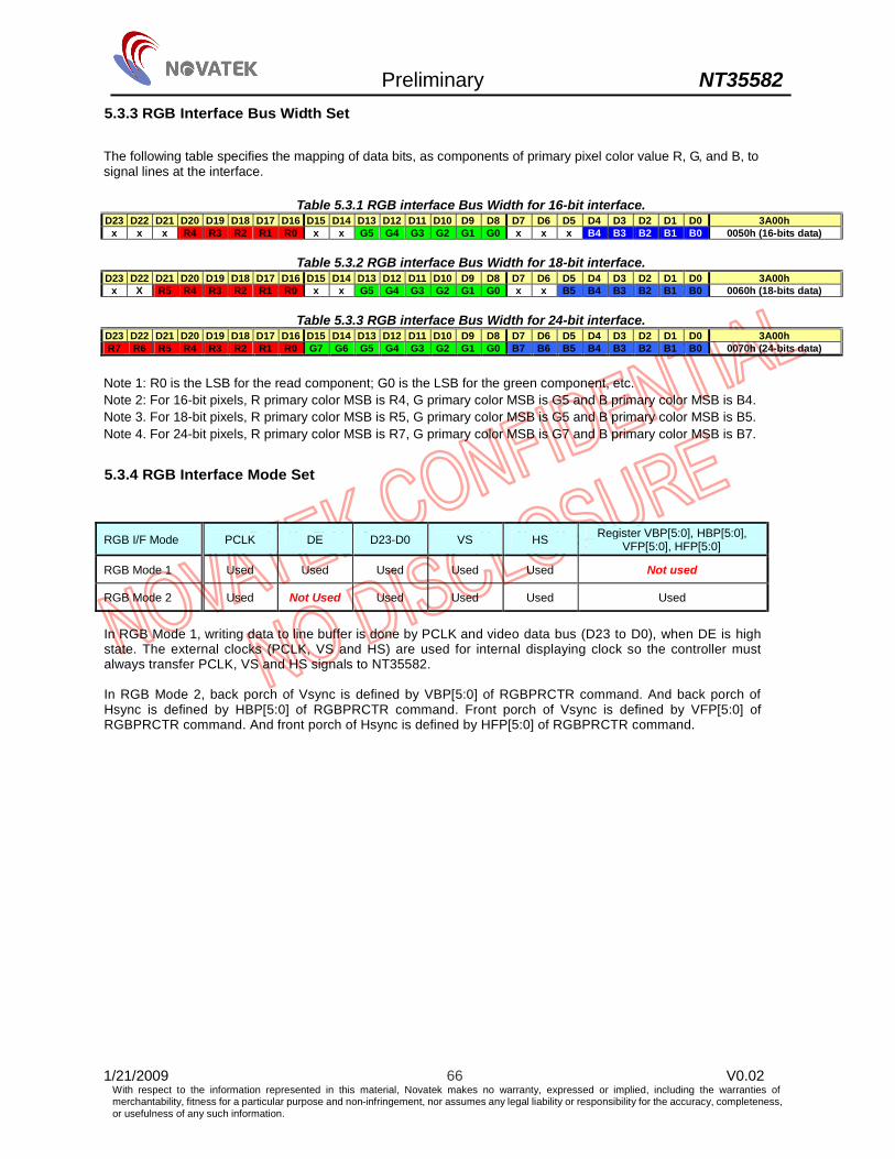
Preliminary NT35582
1/21/2009 66 V0.02 With respect to the information represented in this material, Novatek makes no warranty, expressed or implied, including the warranties of merchantability, fitness for a particular purpose and non-infringement, nor assumes any legal liability or responsibility for the accuracy, completeness, or usefulness of any such information.
5.3.3 RGB Interface Bus Width Set
The following table specifies the mapping of data bits, as components of primary pixel color value R, G, and B, to signal lines at the interface.
Table 5.3.1 RGB interface Bus Width for 16-bit interface. D23 D22 D21 D20 D19 D18 D17 D16 D15 D14 D13 D12 D11 D10 D9 D8 D7 D6 D5 D4 D3 D2 D1 D0 3A00h
x x x R4 R3 R2 R1 R0 x x G5 G4 G3 G2 G1 G0 x x x B4 B3 B2 B1 B0 0050h (16-bits data)
Table 5.3.2 RGB interface Bus Width for 18-bit interface. D23 D22 D21 D20 D19 D18 D17 D16 D15 D14 D13 D12 D11 D10 D9 D8 D7 D6 D5 D4 D3 D2 D1 D0 3A00h
x X R5 R4 R3 R2 R1 R0 x x G5 G4 G3 G2 G1 G0 x x B5 B4 B3 B2 B1 B0 0060h (18-bits data)
Table 5.3.3 RGB interface Bus Width for 24-bit interface. D23 D22 D21 D20 D19 D18 D17 D16 D15 D14 D13 D12 D11 D10 D9 D8 D7 D6 D5 D4 D3 D2 D1 D0 3A00h R7 R6 R5 R4 R3 R2 R1 R0 G7 G6 G5 G4 G3 G2 G1 G0 B7 B6 B5 B4 B3 B2 B1 B0 0070h (24-bits data)
Note 1: R0 is the LSB for the read component; G0 is the LSB for the green component, etc. Note 2: For 16-bit pixels, R primary color MSB is R4, G primary color MSB is G5 and B primary color MSB is B4. Note 3. For 18-bit pixels, R primary color MSB is R5, G primary color MSB is G5 and B primary color MSB is B5. Note 4. For 24-bit pixels, R primary color MSB is R7, G primary color MSB is G7 and B primary color MSB is B7.
5.3.4 RGB Interface Mode Set
RGB I/F Mode PCLK DE D23-D0 VS HS Register VBP[5:0], HBP[5:0], VFP[5:0], HFP[5:0]
RGB Mode 1 Used Used Used Used Used Not used
RGB Mode 2 Used Not Used Used Used Used Used
In RGB Mode 1, writing data to line buffer is done by PCLK and video data bus (D23 to D0), when DE is high state. The external clocks (PCLK, VS and HS) are used for internal displaying clock so the controller must always transfer PCLK, VS and HS signals to NT35582. In RGB Mode 2, back porch of Vsync is defined by VBP[5:0] of RGBPRCTR command. And back porch of Hsync is defined by HBP[5:0] of RGBPRCTR command. Front porch of Vsync is defined by VFP[5:0] of RGBPRCTR command. And front porch of Hsync is defined by HFP[5:0] of RGBPRCTR command.
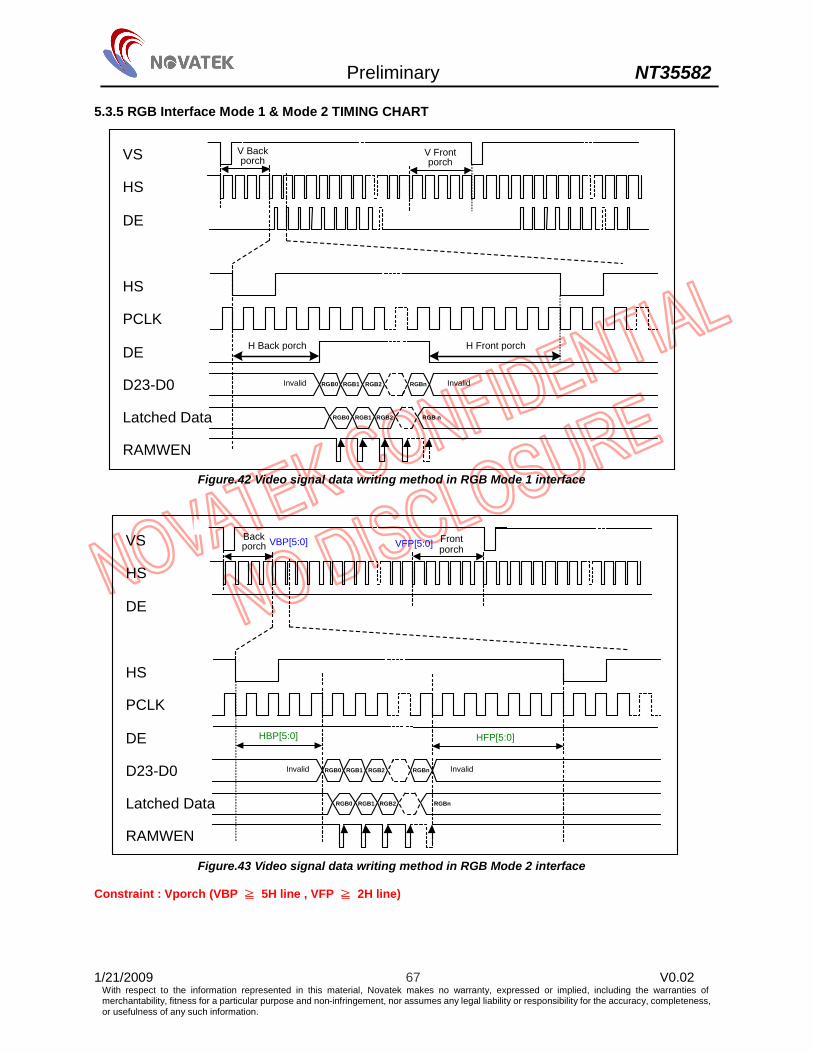
Preliminary NT35582
1/21/2009 67 V0.02 With respect to the information represented in this material, Novatek makes no warranty, expressed or implied, including the warranties of merchantability, fitness for a particular purpose and non-infringement, nor assumes any legal liability or responsibility for the accuracy, completeness, or usefulness of any such information.
5.3.5 RGB Interface Mode 1 & Mode 2 TIMING CHART
RGB0 RGB1 RGB2 RGBn Invalid
RGB0 RGB1 RGB2 RGB n
VS
HS
DE
HS
PCLK
DE
D23D0
Latched Data
RAMWEN
V Front porch
V Back porch
Invalid
H Back porch H Front porch
Figure.42 Video signal data writing method in RGB Mode 1 interface
VBP[5:0]
HBP[5:0]
RGB0 RGB1 RGB2 RGBn Invalid
RGB0 RGB1 RGB2 RGBn
VS
HS
DE
HS
PCLK
DE
D23D0
Latched Data
RAMWEN
Frontporch
Invalid
VFP[5:0]
HFP[5:0]
Back porch
Figure.43 Video signal data writing method in RGB Mode 2 interface
Constraint : Vporch (VBP ≧ 5H line , VFP ≧ 2H line)
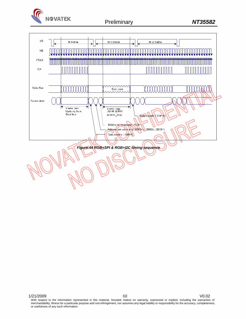
Preliminary NT35582
1/21/2009 68 V0.02 With respect to the information represented in this material, Novatek makes no warranty, expressed or implied, including the warranties of merchantability, fitness for a particular purpose and non-infringement, nor assumes any legal liability or responsibility for the accuracy, completeness, or usefulness of any such information.
Figure.44 RGB+SPI & RGB+I2C timing sequence

Preliminary NT35582
1/21/2009 69 V0.02 With respect to the information represented in this material, Novatek makes no warranty, expressed or implied, including the warranties of merchantability, fitness for a particular purpose and non-infringement, nor assumes any legal liability or responsibility for the accuracy, completeness, or usefulness of any such information.
5.3.6 RGB Interface ICM mode The ICM mode setting GRAM Write/Read frequency and data input select on the RGB interface
Write/ Read frequency and input data select ICM
Write cycle Read cycle Data input 0 PCLK PCLK D[23:0]
1 SDI/I2C_SDA Internal
oscillator SDI/I2C_SDA
When setting ICM = 0 (Exit SRAM data display), It must consider the frame data synchronous for display smooth. The RGB VS signal need to synchronous the FTE signal.
FTE
VS(EXTERNAL)
ICM = 0 command
STV
VS(INTERNAL)
Internal RAM Display
External RGB interface Display
VS synchronouswith FTE signal

Preliminary NT35582
1/21/2009 70 V0.02 With respect to the information represented in this material, Novatek makes no warranty, expressed or implied, including the warranties of merchantability, fitness for a particular purpose and non-infringement, nor assumes any legal liability or responsibility for the accuracy, completeness, or usefulness of any such information.
5.4 I2C Interface The I2C-bus is for bi-directional, two-line communication between different ICs or modules. The two lines are the Serial Data line (I2C_SDA) and the Serial Clock Line (I2C_SCL). Both lines must be connected to a positive supply via pull-up resistors. Data transfer can be initiated only when the bus is not busy. Each byte of eight bits is followed by an acknowledge bit. The acknowledge bit is a HIGH level signal put on the bus by the transmitter during which time the master generates an extra acknowledgement related clock pulse. A slave receiver which is addressed must generate an acknowledgement after the reception of each byte. Also a master receiver must generate an acknowledgement after the reception of each byte that has been clocked out of the slave transmitter. (a) I2C-Bus Protocol
Before any data is transmitted on the I2C-bus, the device which should respond is addressed first. There are four slave addresses can be selected by MCU. The slave address is always carried out with the first byte transmitted after the START procedure.
Figure.45 Definition of I2C-Bus protocol
(b) Definitions - Transmitter: the device which sends the data to the bus. - Receiver: the device which receives the data from the bus. - Master: the device which initiates a transfer, generates clock signals and terminates a transfer. - Slave: the device addressed by a master. - Multi-master: more than one master can attempt to control the bus at the same time without corrupting the message. - Arbitration: procedure to ensure that, if more than one master simultaneously tries to control the bus, only one is allowed to do so and the message is not corrupted. - Synchronization: procedure to synchronize the clock signals of two or more devices.
MASTERTRANSMITTER
/RECEIVER
SLAVERECEIVER
SLAVETRANSMITTER
/RECEIVER
MASTERTRANSMITTER
MASTERTRANSMITTER
/RECEIVER
SDA
SCL
Figure.46 System configuration
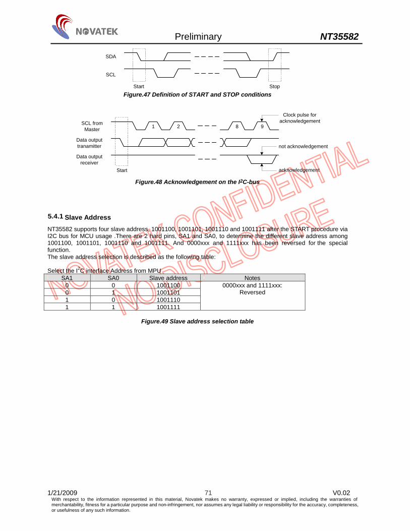
Preliminary NT35582
1/21/2009 71 V0.02 With respect to the information represented in this material, Novatek makes no warranty, expressed or implied, including the warranties of merchantability, fitness for a particular purpose and non-infringement, nor assumes any legal liability or responsibility for the accuracy, completeness, or usefulness of any such information.
SDA
SCL
Start Stop Figure.47 Definition of START and STOP conditions
SCL fromMaster
Start
1 2 8 9
Data outputtranamitter
Data outputreceiver
Clock pulse foracknowledgement
not acknowledgement
acknowledgement
Figure.48 Acknowledgement on the I2C-bus
5.4.1 Slave Address
NT35582 supports four slave address, 1001100, 1001101, 1001110 and 1001111 after the START procedure via I2C bus for MCU usage .There are 2 hard pins, SA1 and SA0, to determine the different slave address among 1001100, 1001101, 1001110 and 1001111. And 0000xxx and 1111xxx has been reversed for the special function. The slave address selection is described as the following table: Select the I2C interface Address from MPU
SA1 SA0 Slave address Notes 0 0 1001100 0 1 1001101 1 0 1001110 1 1 1001111
0000xxx and 1111xxx: Reversed
Figure.49 Slave address selection table
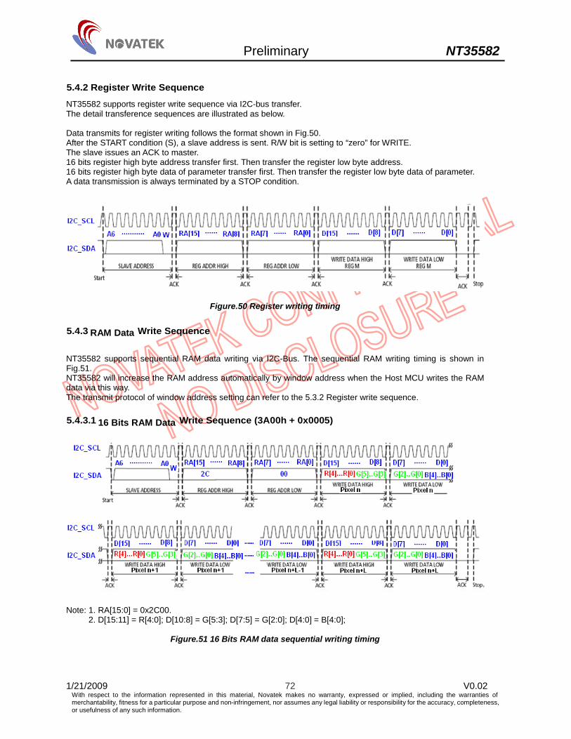
Preliminary NT35582
1/21/2009 72 V0.02 With respect to the information represented in this material, Novatek makes no warranty, expressed or implied, including the warranties of merchantability, fitness for a particular purpose and non-infringement, nor assumes any legal liability or responsibility for the accuracy, completeness, or usefulness of any such information.
5.4.2 Register Write Sequence
NT35582 supports register write sequence via I2C-bus transfer. The detail transference sequences are illustrated as below. Data transmits for register writing follows the format shown in Fig.50. After the START condition (S), a slave address is sent. R/W bit is setting to “zero” for WRITE. The slave issues an ACK to master. 16 bits register high byte address transfer first. Then transfer the register low byte address. 16 bits register high byte data of parameter transfer first. Then transfer the register low byte data of parameter. A data transmission is always terminated by a STOP condition.
Figure.50 Register writing timing
5.4.3 RAM Data Write Sequence
NT35582 supports sequential RAM data writing via I2C-Bus. The sequential RAM writing timing is shown in Fig.51. NT35582 will increase the RAM address automatically by window address when the Host MCU writes the RAM data via this way. The transmit protocol of window address setting can refer to the 5.3.2 Register write sequence. 5.4.3.1 16 Bits RAM Data Write Sequence (3A00h + 0x0005)
Note: 1. RA[15:0] = 0x2C00.
2. D[15:11] = R[4:0]; D[10:8] = G[5:3]; D[7:5] = G[2:0]; D[4:0] = B[4:0];
Figure.51 16 Bits RAM data sequential writing timing

Preliminary NT35582
1/21/2009 73 V0.02 With respect to the information represented in this material, Novatek makes no warranty, expressed or implied, including the warranties of merchantability, fitness for a particular purpose and non-infringement, nor assumes any legal liability or responsibility for the accuracy, completeness, or usefulness of any such information.
5.4.3.2 18 Bits RAM data write Sequence (3A00h + 0x0006)
Note: 1. RA[15:0] = 0x2C00.
2. D[23:22] = D[15:14] = D[7:6] = 0x00; 3. D[21:16] = R[5:0]; D[13:8] = G[5:0]; D[5:0] = B[5:0];
Figure.52 18 Bits RAM data sequential writing timing
5.4.3.3 24 Bits RAM data write Sequence (3A00h + 0x0007)
Note: 1. RA[15:0] = 0x2C00.
2. D[23:16] = R[7:0]; D[15:8] = G[7:0]; D[7:0] = B[7:0];
Figure.53 24 Bits RAM data sequential writing timing

Preliminary NT35582
1/21/2009 74 V0.02 With respect to the information represented in this material, Novatek makes no warranty, expressed or implied, including the warranties of merchantability, fitness for a particular purpose and non-infringement, nor assumes any legal liability or responsibility for the accuracy, completeness, or usefulness of any such information.
5.4.4 Register Read Sequence
NT35582 supports register read sequence via I2C-bus transfer. Register data reading transfers follow the format and is shown in Fig.54.
Figure.54 Register reading timing
5.4.5 RAM Data Read Sequence
NT35582 supports RAM data read function. The RAM data reading timing is shown in Fig.55. The master MCU needs to send the RAM address of reading first and transfer protocol can refer to the Fig.50 Register write sequence. Then the master MCU needs to send the RAM data read register “2E00h” to NT35582. And finally, the MCU can send the following RAM data reading timing to feedback single RAM data value by one complete I2C packet. The example of 16 bits RAM data reading timing is illustrated below.
Figure.55 The example of 16 bits RAM data reading timing
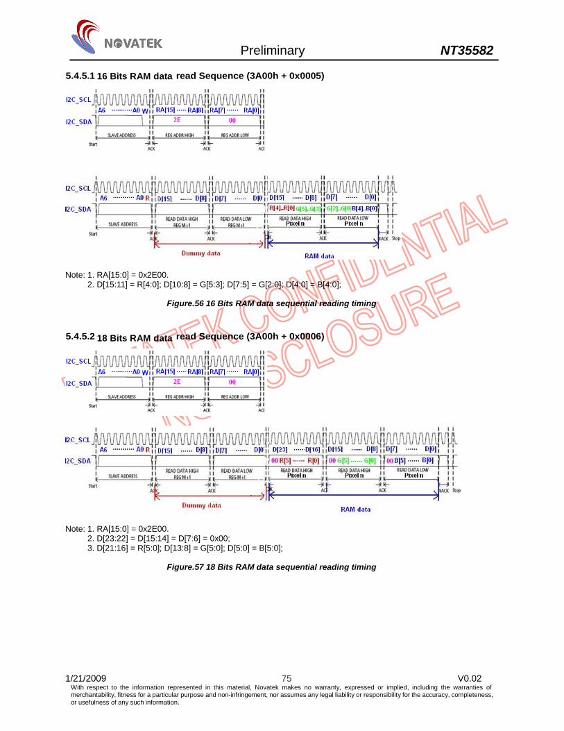
Preliminary NT35582
1/21/2009 75 V0.02 With respect to the information represented in this material, Novatek makes no warranty, expressed or implied, including the warranties of merchantability, fitness for a particular purpose and non-infringement, nor assumes any legal liability or responsibility for the accuracy, completeness, or usefulness of any such information.
5.4.5.1 16 Bits RAM data read Sequence (3A00h + 0x0005)
Note: 1. RA[15:0] = 0x2E00.
2. D[15:11] = R[4:0]; D[10:8] = G[5:3]; D[7:5] = G[2:0]; D[4:0] = B[4:0];
Figure.56 16 Bits RAM data sequential reading timing
5.4.5.2 18 Bits RAM data read Sequence (3A00h + 0x0006)
Note: 1. RA[15:0] = 0x2E00.
2. D[23:22] = D[15:14] = D[7:6] = 0x00; 3. D[21:16] = R[5:0]; D[13:8] = G[5:0]; D[5:0] = B[5:0];
Figure.57 18 Bits RAM data sequential reading timing
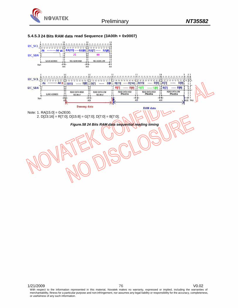
Preliminary NT35582
1/21/2009 76 V0.02 With respect to the information represented in this material, Novatek makes no warranty, expressed or implied, including the warranties of merchantability, fitness for a particular purpose and non-infringement, nor assumes any legal liability or responsibility for the accuracy, completeness, or usefulness of any such information.
5.4.5.3 24 Bits RAM data read Sequence (3A00h + 0x0007)
Note: 1. RA[15:0] = 0x2E00.
2. D[23:16] = R[7:0]; D[15:8] = G[7:0]; D[7:0] = B[7:0];
Figure.58 24 Bits RAM data sequential reading timing

Preliminary NT35582
1/21/2009 77 V0.02 With respect to the information represented in this material, Novatek makes no warranty, expressed or implied, including the warranties of merchantability, fitness for a particular purpose and non-infringement, nor assumes any legal liability or responsibility for the accuracy, completeness, or usefulness of any such information.
5.5 Frame Tearing Effect Interface The frame tearing effect (FTE) signal can be used by the MPU to synchronize frame memory writing to achieve video images displaying without tearing effect. The FTE pulse output position can be specified to the line established by the FTE setting, and should be set in keeping with the data transfer speed. In FTE mode, the data displayed on the panel is written to the internal RAM. In this way, only the data to be written within the moving picture RAM area is transferred, the overall data transfer needed for the moving picture display is minimized. The NT35582 can transfer data via the FTE interface at high speed with reduced power consumption by utilizing the high-speed write function (HSM =1) to write data.
5.5.1 Example 1: MPU Write is Faster than Panel Read Data write to Frame Memory is now synchronized to the panel scan. It should be written next one horizontal sync pulse after FTE signal. This ensures that data is always written ahead of the panel scan and each panel frame refresh has a complete new image.
Figure.59 Example 1: MPU write is faster than panel read

Preliminary NT35582
1/21/2009 78 V0.02 With respect to the information represented in this material, Novatek makes no warranty, expressed or implied, including the warranties of merchantability, fitness for a particular purpose and non-infringement, nor assumes any legal liability or responsibility for the accuracy, completeness, or usefulness of any such information.
5.5.2 Example 2: MPU Write is Slower than Panel Read The MPU to Frame Memory write begins just after Panel Read has commenced. This allows time for the image to download behind the Panel Read pointer and to finish downloading during the subsequent Frame before the Read Pointer “catches” the MPU to Frame memory write position.
Data to be sent
Image on LCD
d e fcba
Figure.60 Example 2: MPU write is slower than panel read
Preliminary NT35582
1/21/2009 79 V0.02 With respect to the information represented in this material, Novatek makes no warranty, expressed or implied, including the warranties of merchantability, fitness for a particular purpose and non-infringement, nor assumes any legal liability or responsibility for the accuracy, completeness, or usefulness of any such information.
The FTE interface has a minimum RAM write speed requirement. Therefore, the RAM Write Speed must be faster than the values calculated from the following formulas:
()16.5(
PorchLinesDisplayLinesfrequencyFrameMHzDisplayClock
>)
Clock per 1 H[Hz]
480 x Display Lines>RAM Write SPEED [Hz](min)
(Display Lines + PorchLines-margins) x RTN x 1Display Clock (16.5MHz) x variance
The following is an example of calculating the minimum RAM writing speed and internal clock frequency in FTE interface operation: [Example]:
Panel size 480 RGB X 800 lines Total number of lines (NOL) 800 lines (NOL = 10’h320) Porch (VPA) 16 lines (VPA = 10h) Frame tearing effect position (FTEP) Display end line: 879th (FTEP = 10’h36F) Frame frequency 60 Hz Display clock 10 MHz
Clocks per 1H (RTN) = 16.5 MHz / (60 Hz × (800 + 16) lines) = 337 clocks Minimum speed for RAM Write [Hz] > 480×800 / (800+16–2)lines×337clocks × 1/(16.5MHz×1.05) = 24.3 MHz Note: 1. In the example, the internal clock frequency allows for a margin of ±5% for variances, and guarantees
that display operation is completed within one FTE cycle. 2. The margin between written data line and the display operation line should be larger than two lines.
3. The FTE pulse output position is set to the line designated by N [9:0].
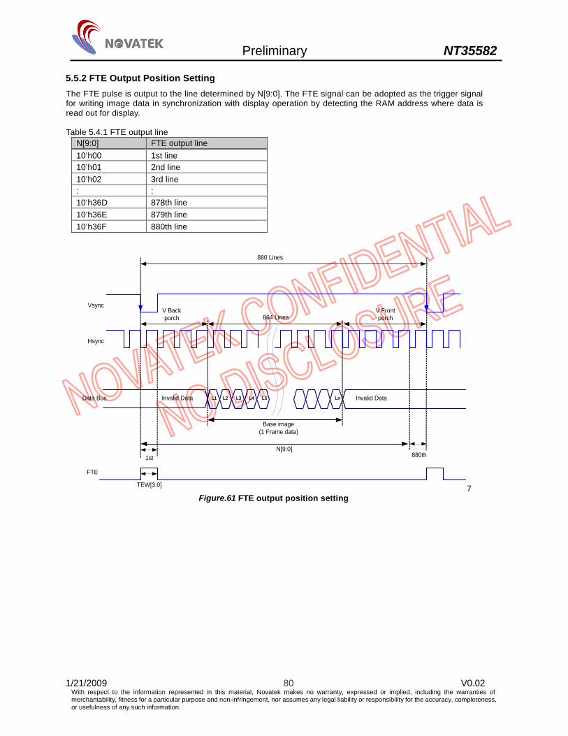
Preliminary NT35582
1/21/2009 80 V0.02 With respect to the information represented in this material, Novatek makes no warranty, expressed or implied, including the warranties of merchantability, fitness for a particular purpose and non-infringement, nor assumes any legal liability or responsibility for the accuracy, completeness, or usefulness of any such information.
5.5.2 FTE Output Position Setting The FTE pulse is output to the line determined by N[9:0]. The FTE signal can be adopted as the trigger signal for writing image data in synchronization with display operation by detecting the RAM address where data is read out for display. Table 5.4.1 FTE output line
N[9:0] FTE output line 10’h00 1st line 10’h01 2nd line 10’h02 3rd line : : 10’h36D 878th line 10’h36E 879th line 10’h36F 880th line
864 LinesV Back porch
L1
Vsync
Base image (1 Frame data)
N[9:0]1st 880th
Data Bus
FTE
V Front porch
Hsync
880 Lines
L2 L3 L4 L5 LnInvalid Data Invalid Data
TEW[3:0] 7 Figure.61 FTE output position setting
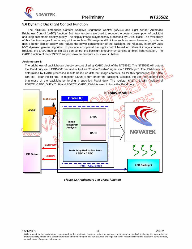
Preliminary NT35582
1/21/2009 81 V0.02 With respect to the information represented in this material, Novatek makes no warranty, expressed or implied, including the warranties of merchantability, fitness for a particular purpose and non-infringement, nor assumes any legal liability or responsibility for the accuracy, completeness, or usefulness of any such information.
5.6 Dynamic Backlight Control Function The NT35582 embedded Content Adaptive Brightness Control (CABC) and Light sensor Automatic
Brightness Control (LABC) function. Both two functions are used to reduce the power consumption of backlight and keep acceptable display quality. The display image is dynamically processed by CABC block. The availability of this function ranges from moving picture such as TV image to still picture such as menu. However, in order to gain a better display quality and reduce the power consumption of the backlight, the NT35582 internally uses NVT dynamic gamma algorithm to produce an optimal backlight control based on different image contents. Besides, the LABC mechanism also can control the backlight smoothly by sensing ambient light variation. The CABC function of the NT35582 supports two architectures as shown in below:
Architecture 1: The brightness of backlight can directly be controlled by CABC block of the NT35582. The NT35582 will output the PWM duty via “LEDPWM” pin, and output an “Enable/Disable” signal via “LEDON pin”. The PWM duty is determined by CABC processed results based on different image contents. As for this application, user also can set / clear the bit “BL” of register 5300h to turn on/off the backlight. Besides, the user can control the brightness of the backlight by forcing a specified PWM duty. The register 6A17h, 6A18h (include of FORCE_CABC_DUTY[7 : 0] and FORCE_CABC_PWM) is used to force the PWM duty.
HOST
LED Driver
Image Histogram Analysis
CABC
PWM Duty Estimation FromLABC + CABC
Driver IC
Full - ABC Block LED Backlight
Display ModuleImage Data
LABC
LEDPWM
LEDON
Figure.62 Architecture 1 of CABC function
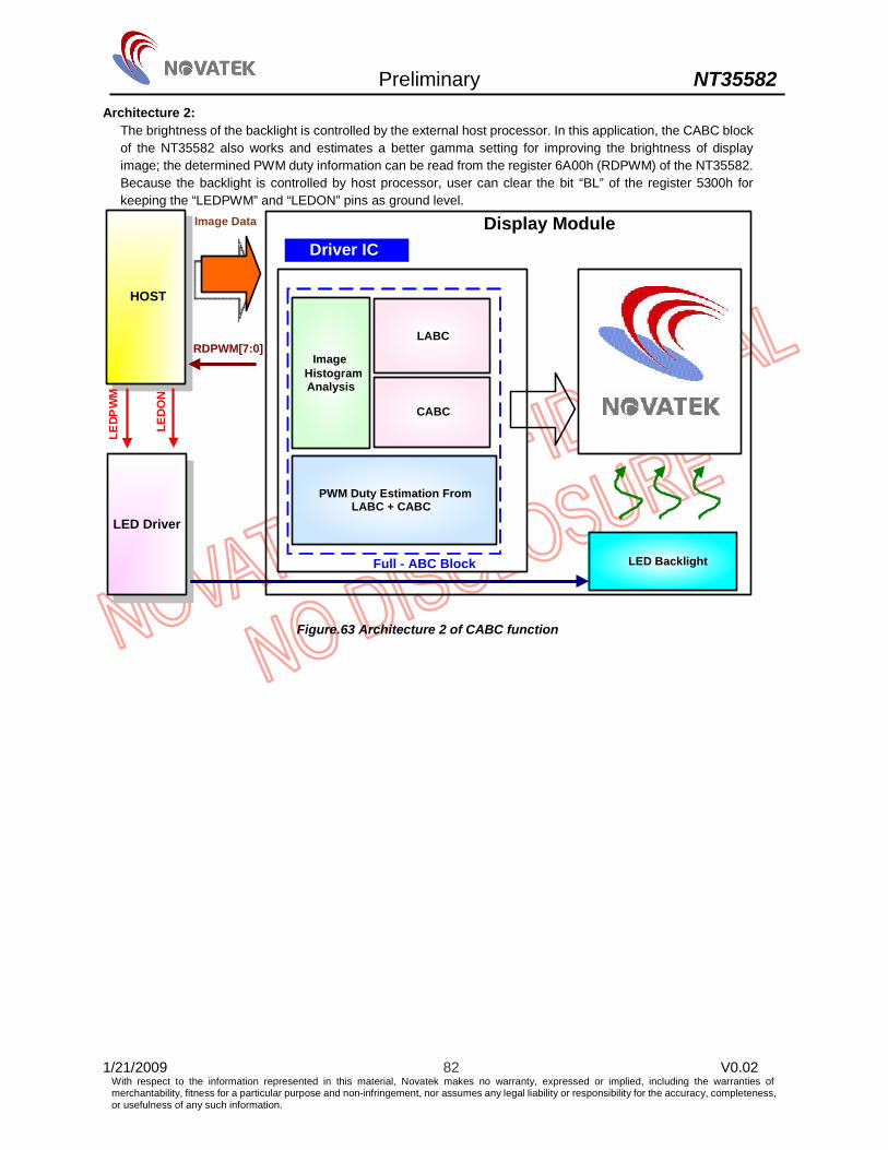
Preliminary NT35582
1/21/2009 82 V0.02 With respect to the information represented in this material, Novatek makes no warranty, expressed or implied, including the warranties of merchantability, fitness for a particular purpose and non-infringement, nor assumes any legal liability or responsibility for the accuracy, completeness, or usefulness of any such information.
Architecture 2: The brightness of the backlight is controlled by the external host processor. In this application, the CABC block of the NT35582 also works and estimates a better gamma setting for improving the brightness of display image; the determined PWM duty information can be read from the register 6A00h (RDPWM) of the NT35582. Because the backlight is controlled by host processor, user can clear the bit “BL” of the register 5300h for keeping the “LEDPWM” and “LEDON” pins as ground level.
HOST
LED Driver
Image Histogram Analysis
CABC
PWM Duty Estimation FromLABC + CABC
Driver IC
Full - ABC Block LED Backlight
Display ModuleImage Data
LABCRDPWM[7:0]
LEDP
WM
LED
ON
Figure.63 Architecture 2 of CABC function
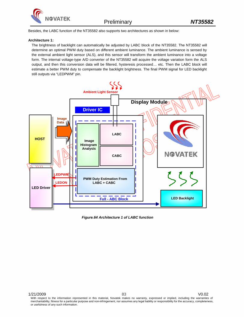
Preliminary NT35582
1/21/2009 83 V0.02 With respect to the information represented in this material, Novatek makes no warranty, expressed or implied, including the warranties of merchantability, fitness for a particular purpose and non-infringement, nor assumes any legal liability or responsibility for the accuracy, completeness, or usefulness of any such information.
Besides, the LABC function of the NT35582 also supports two architectures as shown in below: Architecture 1: The brightness of backlight can automatically be adjusted by LABC block of the NT35582. The NT35582 will determine an optimal PWM duty based on different ambient luminance. The ambient luminance is sensed by the external ambient light sensor (ALS), and this sensor will transform the ambient luminance into a voltage form. The internal voltage-type A/D converter of the NT35582 will acquire the voltage variation form the ALS output, and then this conversion data will be filtered, hysteresis processed… etc. Then the LABC block will estimate a better PWM duty to compensate the backlight brightness. The final PWM signal for LED backlight still outputs via “LEDPWM” pin.
HOST
LED Driver
Image Histogram Analysis
CABC
PWM Duty Estimation FromLABC + CABC
Driver IC
Full - ABC Block LED Backlight
LEDPWM
LEDON
Display Module
Image Data
LABC
Ambient Light Sensor
Figure.64 Architecture 1 of LABC function
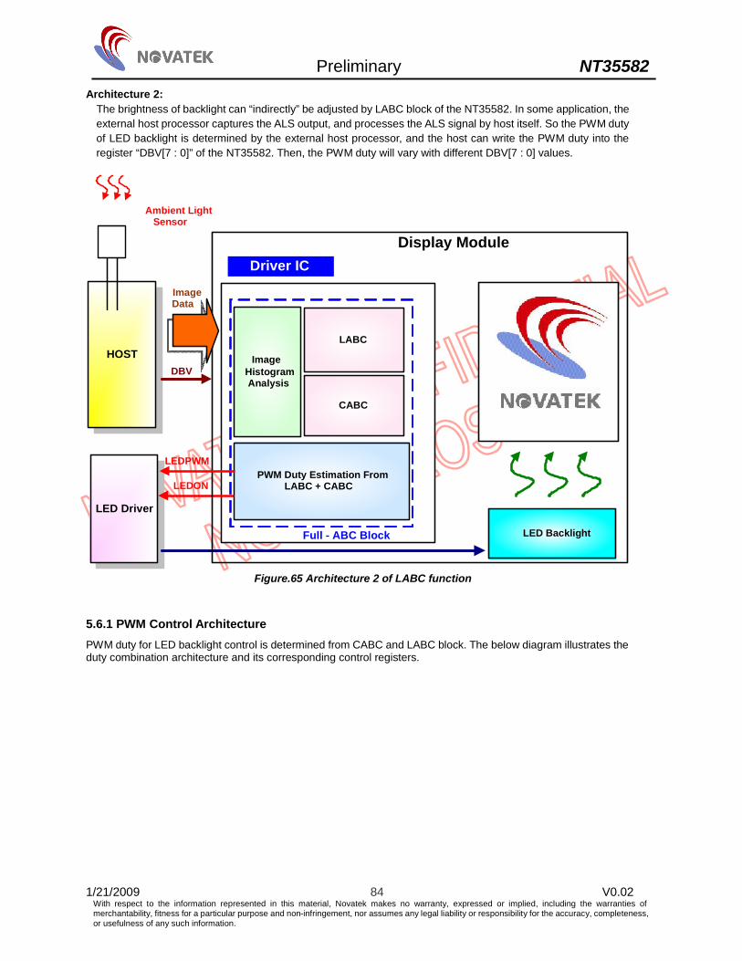
Preliminary NT35582
1/21/2009 84 V0.02 With respect to the information represented in this material, Novatek makes no warranty, expressed or implied, including the warranties of merchantability, fitness for a particular purpose and non-infringement, nor assumes any legal liability or responsibility for the accuracy, completeness, or usefulness of any such information.
Architecture 2: The brightness of backlight can “indirectly” be adjusted by LABC block of the NT35582. In some application, the external host processor captures the ALS output, and processes the ALS signal by host itself. So the PWM duty of LED backlight is determined by the external host processor, and the host can write the PWM duty into the register “DBV[7 : 0]” of the NT35582. Then, the PWM duty will vary with different DBV[7 : 0] values.
HOST
LED Driver
Image Histogram Analysis
CABC
PWM Duty Estimation FromLABC + CABC
Driver IC
Full - ABC Block LED Backlight
LEDPWM
LEDON
Display Module
Image Data
LABC
Ambient Light Sensor
DBV
Figure.65 Architecture 2 of LABC function
5.6.1 PWM Control Architecture PWM duty for LED backlight control is determined from CABC and LABC block. The below diagram illustrates the duty combination architecture and its corresponding control registers.
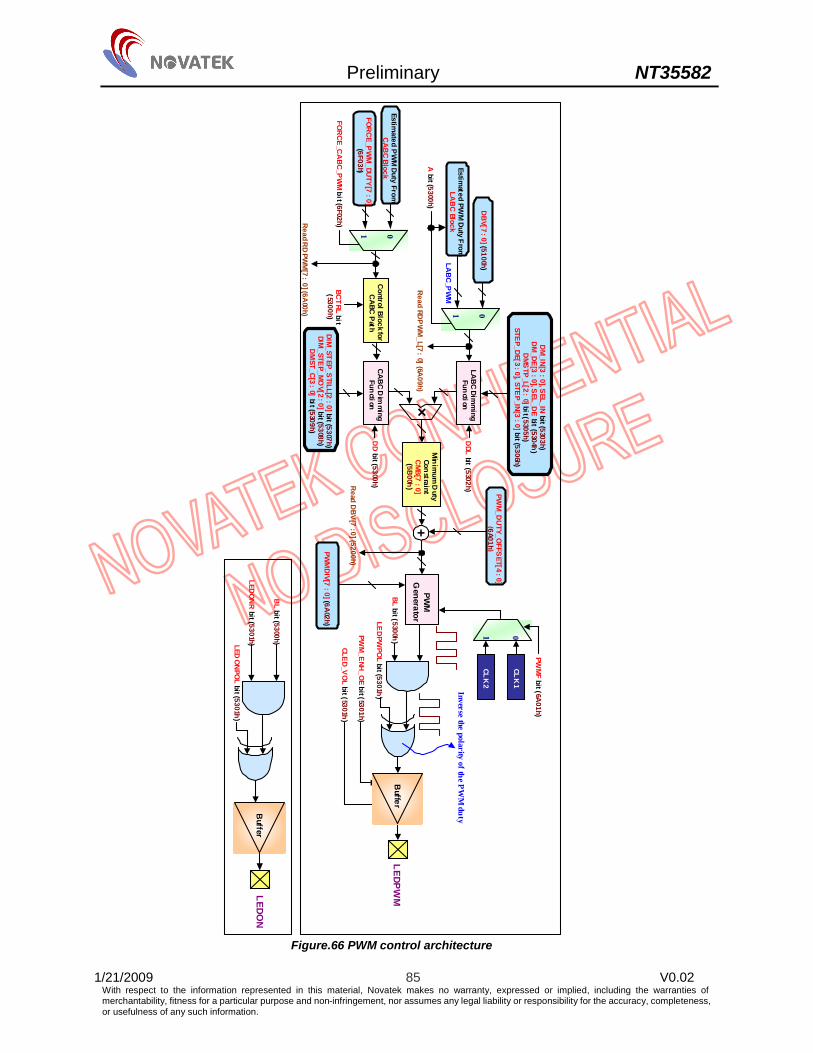
Preliminary NT35582
1/21/2009 85 V0.02 With respect to the information represented in this material, Novatek makes no warranty, expressed or implied, including the warranties of merchantability, fitness for a particular purpose and non-infringement, nor assumes any legal liability or responsibility for the accuracy, completeness, or usefulness of any such information.
PWM
Generator
BLbit(5300h
)
LED
PWPO
Lbit(5301h
)
CLED
_VO
Lbit(5301h)
LEDPW
MB
uffer
Inversethe
polarityofthePW
Mduty
PWM
_ENH
_OE
bit(5301h)
Min
imum
Duty
Constraint
CM
B[7:0]
(5B00h)
+
PWM
DIV[7
:0](6A02h)
PWM
_DU
TY_OFFS
ET[4:0]
(6A01h)
CA
BC
Dim
mingFun
ction ×
DD
bit(5300h)
LAB
CDim
ming
Function
DDL
bit(5302h)
DIM_ST
EP_STILL[2
:0]bit(5307h)DIM
_STEP_M
OV[2
:0]bit(5308h)D
MST_C[3
:0]
bit(5309h)
DM
_IN[3:0],S
EL_INbit(5303h)
DM
_DE
[3:0],S
EL_DE
bit(5304h
)D
MS
TP_L[2
:0]bit(5305h)
STEP_D
E[3:0],STE
P_IN
[3:0]bit(5306h)
Estimated
PW
MD
utyFrom
CA
BC
Block
FOR
CE
_PW
M_DU
TY[7
:0](6F03h)
01
ControlBlock
forC
ABC
Path
BCT
RLbit
(5300h)FO
RC
E_C
AB
C_P
WM
bit(6F02h)Read
RD
PWM
[7:
0](6A00h)
Read
DB
V[7
:0](5200h)
Estimated
PWM
Duty
FromLA
BC
Block
01
Abit(5300h) D
BV[7
:0](5100h)
Read
RDP
WM
_L[7:
0](6A
09h)
Buffer
LEDON
LEDO
NPO
Lbit(5301h)
BL
bit(5300h)
LEDO
NR
bit(5301h)
LAB
C_P
WM
CLK
2
CLK
101
PWM
Fbit(6A
01h)
Figure.66 PWM control architecture

Preliminary NT35582
1/21/2009 86 V0.02 With respect to the information represented in this material, Novatek makes no warranty, expressed or implied, including the warranties of merchantability, fitness for a particular purpose and non-infringement, nor assumes any legal liability or responsibility for the accuracy, completeness, or usefulness of any such information.
The register bit “BL” is used to control the “LEDPWM” pin to output PWM signal; here are listed some applications in below table:
BL LEDPWPOL Status of LEDPWM 0 0 0 (Default) 0 1 1 1 0 Original polarity of PWM signal 1 1 Inversed polarity of PWM signal
In the same way, “BL” is used to make the “LEDON” pin in a fixed logical state; here are listed some applications in below table:
BL LEDONPOL Status of LEDON 0 0 0 (Default) 0 1 1 1 0 LEDONR 1 1 Inversed LEDONR
The setting bit “PWM_ENH_OE” is applied to improvement the driving ability of “LEDPWM” pin; here are listed two driving abilities for selection:
PWM_ENH_OE Status of LEDON 0 1X driving ability of LEDPWM 1 2X driving ability of LEDPWM
The setting bit “CLED_VOL” is applied to choose two different logical voltage levels for “LEDPWM” and “LEDON” pins:
CLED_VOL Logical Voltage Level for LEDPWM and LEDON 0 VDDI <-> Vss (Default) 1 VCI <-> Vss
The registers PWMDIV[7 : 0] and PWM_DUTY_OFFSET[4 : 0] can change the frequency and duty compensation of the PWM signal. For NT35582, the PWM operation frequency “FOSC” can be selected by the register bit “PWMF”, so two PWM operation frequencies can be selected as shown in below table:
Register Bit “PWMF” PWM Operation Frequency – “FOSC” 0 5.5 MHz (Default) 1 11 MHz
The PWM operation frequency “FOSC” is “not” the real PWM frequency, the “FOSC” is used to provide clock source for the internal PWM circuit. Actually, the real PWM frequency can be quickly estimated by the bellow formula:
]0:7[256 Frequency PWM
PWMDIVFOSC

Preliminary NT35582
1/21/2009 87 V0.02 With respect to the information represented in this material, Novatek makes no warranty, expressed or implied, including the warranties of merchantability, fitness for a particular purpose and non-infringement, nor assumes any legal liability or responsibility for the accuracy, completeness, or usefulness of any such information.
So the relations between “PWMF”, “FOSC”, actually PWM frequency are shown in below table:
Register Bit “PWMF” PWM Operation Frequency – “FOSC” Real PWM Frequency 0 5.5 MHz (Default)
]0:7[256MHz 5.5
PWMDIV
1 11 MHz
]0:7[256MHz 11
PWMDIV
For Example: If the PWMDIV[7:0] = 0Ch, and PWMF = 0, then:
KHz 79.121256
MHz 5.5]0:7[256
5.5MHz Frequency PWM
PWMDIV
In this condition, when PWM duty is estimated as “3” (Reading the register “DBV[7:0]” = 02h), then the duty time of the PWM Signal can be estimated as shown in below:
sec 54.6KHz 79.11
2563 TimeDuty PWM
msec 552.0KHz 79.11
2563)-(256 Timeduty -Non PWM
The above duty calculations can be illustrated in below for detailed:
PW
MSi
gnal
ofLE
DP
WM
Pin
Figure.67 PWM signal of LEDPWM pin
In the other way, there are some registers are simply introduced in below (See the chapter 6 for details): DBV[7:0]: Writing this register in address 5100h is used to adjust the backlight brightness value when LABC
function of the NT35582 is disabled (means the register bit “A” is set as “0”). However, reading this register from address 5200h is used to indicate the real PWM duty variation.
CMB[7:0]: This register setting is used to limit the minimum PWM duty in order to prevent the backlight
brightness too dark. FORCE_CABC_DUTY[7:0]: This register is used to perform a fixed PWM duty of CABC output while the register
bit “FORCE_CABC_PWM” is set as “1”. Because the external LED driver needs some rising time to driver the LED backlight, this necessary rising time will reduce the effective PWM duty period, so the PWM_DUTY_OFFSET[4:0] is used to compensate effective PWM duty.
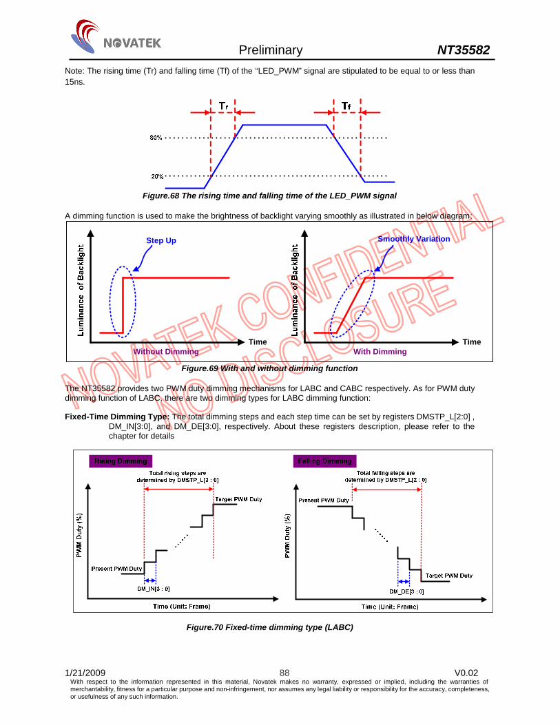
Preliminary NT35582
1/21/2009 88 V0.02 With respect to the information represented in this material, Novatek makes no warranty, expressed or implied, including the warranties of merchantability, fitness for a particular purpose and non-infringement, nor assumes any legal liability or responsibility for the accuracy, completeness, or usefulness of any such information.
Note: The rising time (Tr) and falling time (Tf) of the “LED_PWM” signal are stipulated to be equal to or less than 15ns.
Figure.68 The rising time and falling time of the LED_PWM signal
A dimming function is used to make the brightness of backlight varying smoothly as illustrated in below diagram:
TimeWithout Dimming
Step Up
TimeWith Dimming
Smoothly Variation
Figure.69 With and without dimming function The NT35582 provides two PWM duty dimming mechanisms for LABC and CABC respectively. As for PWM duty dimming function of LABC, there are two dimming types for LABC dimming function: Fixed-Time Dimming Type: The total dimming steps and each step time can be set by registers DMSTP_L[2:0] ,
DM_IN[3:0], and DM_DE[3:0], respectively. About these registers description, please refer to the chapter for details
Figure.70 Fixed-time dimming type (LABC)
Preliminary NT35582
1/21/2009 89 V0.02 With respect to the information represented in this material, Novatek makes no warranty, expressed or implied, including the warranties of merchantability, fitness for a particular purpose and non-infringement, nor assumes any legal liability or responsibility for the accuracy, completeness, or usefulness of any such information.
Fixed-Slope Dimming Type: The increasing / decreasing PWM duty and each step time can be set by register STEP_IN[3:0], STEP_DE[3:0], DM_IN[3:0], and DM_DE[3:0, respectively. About these registers description, please refer to the chapter for details
PW
M D
uty
(%)
PWM
Dut
y (%
)
Figure.71 Fixed-slope dimming type (LABC)
As for PWM duty dimming function of CABC, there is only one dimming type “Fixed-Time Dimming” for CABC dimming function, and the rising dimming and the falling dimming use the same registers for setting (“DIM_STEP_STILL[2:0] and DMST_C[3:0]”, or “DIM_STEP_MOV[2:0] and DMST_C[3:0]”). About these registers description, please refer to the chapter for details:
PWM
Dut
y (%
)
PWM
Dut
y (%
)
Figure.72 Dimming Mechanism in CABC Still Mode
PWM
Dut
y (%
)
PWM
Dut
y (%
)
Figure. 73 Dimming Mechanism in CABC Moving Mode

Preliminary NT35582
1/21/2009 90 V0.02 With respect to the information represented in this material, Novatek makes no warranty, expressed or implied, including the warranties of merchantability, fitness for a particular purpose and non-infringement, nor assumes any legal liability or responsibility for the accuracy, completeness, or usefulness of any such information.
5.6.2 Content Adaptive Brightness Control (CABC) A Content Adaptive Brightness Control (CABC) function can be used to reduce the power consumption of the
luminance source. Content adaptation means that content grey level scale can be increased while simultaneously decreasing brightness of the backlight to achieve same perceived brightness. The adjusted grey level scale and thus the power consumption reduction depend on the content of the image. The NVT CABC algorithm can adjust the brightness of each gray level without changing the original image contents.
The NVT CABC function provides four operation modes, and these modes can be selected by the register 5500h. See command “Write Content Adaptive Brightness Control (5500h)” (CABC_COND[1:0]) for more information. These four modes are described as below: - Off Mode:
Content Adaptive Brightness Control functionality is completely turn-off. In this mode, the NT35582 will use the original Gamma 2.2 registers setting for display. And if the function of “forced PWM duty” is turn-off (i.e. “FORCE_CABC_PWM” is set as ‘0’), the PWM duty of the “LEDPWM” pin is 100%.
- UI [User interface] Image Mode (UI Mode):
This mode is applied to optimize for UI image. It is kept image quality as much as possible. Target power consumption reduction ratio: 10% or less. NT35582 provides flexible configuration for UI-Mode by setting the registers 6A04h ~ 6A07h (CABC_UI_PWM0[7:0] ~ CABC_UI_PWM3[7:0]) to setting prefer brightness.
- Still Picture Mode (Still Mode):
This mode is used to gain a better display quality for still picture. Some image quality degradation would be acceptable. Ideal power consumption reduction ratio is more than 30%. The NT35582 will automatically estimate a better gamma setting and PWM duty based on different image contents, so the reduction ratio of the power consumption of backlight is not a constant ratio, this ratio will vary between 10% ~ 40% with different image contents.
- Moving Image Mode (Moving Mode):
User can select this mode to keep the moving image quality and reduce the power consumption of backlight. It is focused on the biggest power reduction with image quality degradation. Idea power consumption reduction ratio is more than 30%.
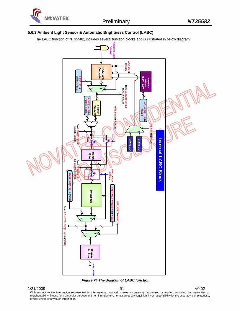
Preliminary NT35582
1/21/2009 91 V0.02 With respect to the information represented in this material, Novatek makes no warranty, expressed or implied, including the warranties of merchantability, fitness for a particular purpose and non-infringement, nor assumes any legal liability or responsibility for the accuracy, completeness, or usefulness of any such information.
5.6.3 Ambient Light Sensor & Automatic Brightness Control (LABC) The LABC function of NT35582, includes several function blocks and is illustrated in below diagram: A
mbientLightSensor
10-bitA/DConverter
FlickerR
emoved
Median
FilterH
ysteresis
ReadFFSV[15
:0]bit(5C
00h,5D00h)
Read
FSV[15:0]bit
(5A00h,5B00h)
ReadA
LSV[15:0]bit
(5A01h,5B
01h)
SW
1
SW
2S
W3
10
Read
RD_H
YST_OU
T[3:0]bit(5F01h)
10
HYST_EN
bit(5E03h)
HYST_W
R[3:0]bit(5E02h)
HYST_O
UT_VA
L[3:0]bit(5E01h)
SET_H
YST
bit(5E03h)M
FR_BYS
bit(5E03h)
DisplayProfiles
LAB
C_PW
M
ADC
_ENbit
(5E03h)
×LSC
C[15:0]bit
(6500h,6501h)
220H
zC
LK
110H
zC
LK
SR_SEL
bit(5E03h)Reference
Voltage(1.6V
~2.3V)
AD
_VRE
F[2:0]bit
(5E04h)
LS[15:0]bit
(6F00h,6F01h)
10
InternalLAB
CBlock
01
Figure.74 The diagram of LABC function
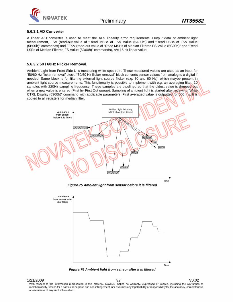
Preliminary NT35582
1/21/2009 92 V0.02 With respect to the information represented in this material, Novatek makes no warranty, expressed or implied, including the warranties of merchantability, fitness for a particular purpose and non-infringement, nor assumes any legal liability or responsibility for the accuracy, completeness, or usefulness of any such information.
5.6.3.1 AD Converter A linear A/D converter is used to meet the ALS linearity error requirements. Output data of ambient light measurement, FSV (read-out value of “Read MSBs of FSV Value (5A00h”) and “Read LSBs of FSV Value (5B00h)” commands) and FFSV (read-out value of “Read MSBs of Median Filtered FS Value (5C00h)” and “Read LSBs of Median Filtered FS Value (5D00h)” commands), are 16 bit linear value.
5.6.3.2 50 / 60Hz Flicker Removal. Ambient Light from Front Side U is measuring white spectrum. These measured values are used as an input for “50/60 Hz flicker removal” block. “50/60 Hz flicker removal” block converts sensor values from analog to a digital if needed. Same block is for filtering external light source flicker (e.g. 50 and 60 Hz), which maybe present in ambient light source measurements. This functionality is possible to implement with e.g. an averaging filter, 10 samples with 220Hz sampling frequency. These samples are pipelined so that the oldest value is dropped out when a new value is entered (First In- First Out queue). Sampling of ambient light is started after receiving “Write CTRL Display (5300h)” command with applicable parameters. First averaged value is outputted for 500 ms. It is copied to all registers for median filter.
Ambient light flickering,which should be filtered
Time
Luminancefrom sensor
before it is filterd
Figure.75 Ambient light from sensor before it is filtered
Time
Luminancefrom sensor after
it is filterd
Figure.76 Ambient light from sensor after it is filtered
Preliminary NT35582
1/21/2009 93 V0.02 With respect to the information represented in this material, Novatek makes no warranty, expressed or implied, including the warranties of merchantability, fitness for a particular purpose and non-infringement, nor assumes any legal liability or responsibility for the accuracy, completeness, or usefulness of any such information.
5.6.3.3 Light Guide Compensation. Filtered luminance value is inputted into “Apply calibration and light guide compensation” block. “Apply calibration and light guide compensation” block is to calibrate measured luminance and to compensate variation of light guide which is covered on the ambient light sensor. Compensated luminance value can be read by the user (16 bit value, see chapters: “Read MSBs of FSV Value (5A00h)” and Read LSBs of FSV Value (5B00h)” without a delay at any time. This doesn’t apply 120ms for SW / HW reset wait time and 500 ms for activated ambient light sensing with “Write CTRL Display (5300h)” command after power on sequence. First measurement is started after the command. This means that display module must apply flicker removal, calibration and compensation into measured values within 500 ms after the activation. 500 ms is the maximum sampling time of the ambient light (the same meaning as median filter input). Output is applied flicker removal, calibration and compensation. Note: The valid value range for register FSV, FFSV, LS, and ALSV is 0 ~ 1023 (Not 0 ~ 65535)

Preliminary NT35582
1/21/2009 94 V0.02 With respect to the information represented in this material, Novatek makes no warranty, expressed or implied, including the warranties of merchantability, fitness for a particular purpose and non-infringement, nor assumes any legal liability or responsibility for the accuracy, completeness, or usefulness of any such information.
5.6.3.4 Median Filter ”Median Filter for Environment Changes" block is filtering information received from “Apply calibration and light guide compensation” block. Median filter receives number of values, which are stored in a queue. The length of the queue is 13 samples and the time between samples is 500 ms. The oldest value stored in the queue is also the first value to drop when a new value is queued. An example of this method is illustrated below.
Time
ReadLuminance
Value
N N+1 N+2 N+3 N+4 N+5 N+6 N+7 N+8 N+9 N+10 N+11 N+12 N+13 N+14 N+15 N+16
Samples on the queue at N+12
Samples on the queue at N+13
Samples on the queue at N+14
Samples on the queue at N+15
65536
Figure.77 An example of median filter for environment changes
Luminance values of this example are defined on the following table:
Time Read Luminance Value
(0 – 65535)
n 40960 n+1 30720 n+2 64000 n+3 32768 n+4 62720 n+5 47360 n+6 51200 n+7 58880 n+8 53760 n+9 40960
n+10 38400 n+11 51200 n+12 47360 n+13 51200 n+14 58880 n+15 53760 n+16 40960
Sampling of ambient light is started after receiving “Write CTRL Display (5300h)” command with applicable parameters. First averaged value should be outputted in 500 ms. Waiting time for V-Sync is not included in 500 ms. The first averaged value is copied to all registers for median filter.

Preliminary NT35582
1/21/2009 95 V0.02 With respect to the information represented in this material, Novatek makes no warranty, expressed or implied, including the warranties of merchantability, fitness for a particular purpose and non-infringement, nor assumes any legal liability or responsibility for the accuracy, completeness, or usefulness of any such information.
5.6.3.5 Hysteresis Hysteresis defines when to change between brightness values. Different values are used to define increment and decrement limits. The user can program these steps, see “Write Hysteresis (5700h)”, “Write Profile Values for Display (5000h)” and ”Write Gamma setting (5800h)”. For each step number ‘n’, the following values are required: • An 8-bit value (Vn) which sets the display brightness. • A 16-bit value (In) ‘increment step’ value. If the output value of the median filter is greater than the previous one, then the In values represent the transition from the step ‘n’ to step ‘n + 1’.
• A 16-bit value (Dn) ‘decrement step’ value. If the output value of the median filter is smaller than the previous one, then the Dn values represent the transition from the step ‘n’ to step ‘n - 1’
• A 4-bit (Gn) ‘gamma curve select’ value. This uses 1-hot encoding to select which gamma curve will be used for each step.
• Maximum step number (n) is 16. The bellow diagram shows a graph of hysteresis input value vs. display backlight output for an arbitrary hysteresis curve. For this graph, step 12 is before the last step in the current profile, and so doesn’t have any increment or decrement step values associated with it. Note: For the last step both increment and decrement values are set to 65535 (FFFFh). E.g. D13 and I13 are set to 65535 (FFFFh) in the case of the below diagram.
Figure.78 The graph of hysteresis input value vs. display backlight output
This curve can be split into two separate cases, one for increasing input, and the other for decreasing input. Once the hysteresis is known to be increasing or decreasing, the diagram shown in above can be separated into the two curves. Once the correct graph is chosen, it is relatively simple to go through each of the levels in turn, checking against the increment or decrement values as necessary.

Preliminary NT35582
1/21/2009 96 V0.02 With respect to the information represented in this material, Novatek makes no warranty, expressed or implied, including the warranties of merchantability, fitness for a particular purpose and non-infringement, nor assumes any legal liability or responsibility for the accuracy, completeness, or usefulness of any such information.
The following table is specified the relationship between each parameters and step number using 6 steps (6 increment and 6 decrement) for hysteresis 6.
Step Number (n) Increment Value (In) Decrement Value (Dn)
Display Brightness (Vn) Gamma Curve (Gn)
1 3840 (F00h) 2560 (A00h) 20 (14h) 2.2 (1h) 2 16896 (4200h) 14336 (3800h) 40(28h) 2.2 (1h) 3 25600 (6400h) 20480 (5000h) 80(50h) 2.2 (1h) 4 35840 (8C00h) 33280 (8200h) 130 (82h) 2.2 (1h) 5 48896 (BF00h) 43776 (AB00h) 200 (C8h) 2.2 (1h) 6 65535 (FFFFh) 65535 (FFFFh) 0 1.0 (8h)
7 X X X X
8 X X X X
9 X X X X 10 X X X X
11 X X X X
12 X X X X
13 X X X X
14 X X X X
15 X X X X
16 X X X X
Step number of increment-value and decrement-value is 16 steps. Don’t care about the parameter values after “65535 (FFFFh)” of increment value and decrement value, e.g. “X” in the above table. The 16th increment and decrement values are always set to “65535 (FFFFh)” internally, if increment and decrement values before 16th parameters are less than “65535 (FFFFh)”. Note: “Read Display Image Mode (0D00h)” command can read the status of whichever is being used by display. For example, if automatic gamma is selected, the value set with “Write Gamma setting (5800h~5807h)” is returned.
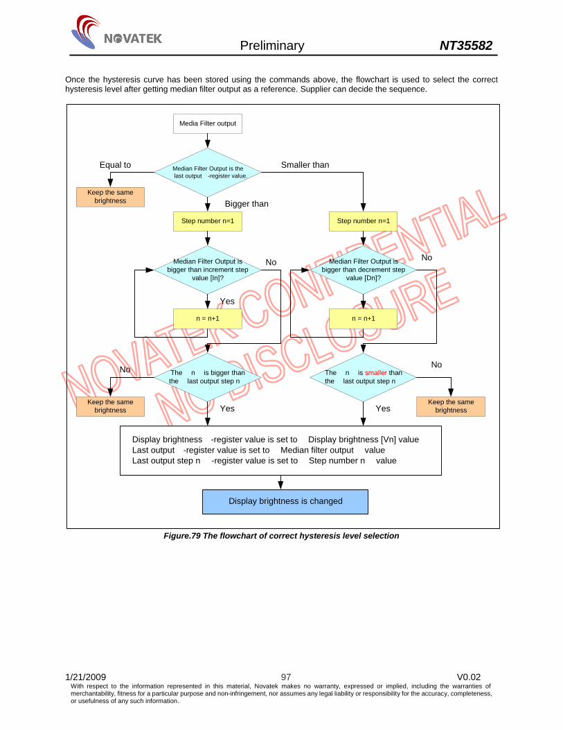
Preliminary NT35582
1/21/2009 97 V0.02 With respect to the information represented in this material, Novatek makes no warranty, expressed or implied, including the warranties of merchantability, fitness for a particular purpose and non-infringement, nor assumes any legal liability or responsibility for the accuracy, completeness, or usefulness of any such information.
Once the hysteresis curve has been stored using the commands above, the flowchart is used to select the correct hysteresis level after getting median filter output as a reference. Supplier can decide the sequence.
Media Filter output
Median Filter Output is the “ last output” -register value.
Step number n=1
Median Filter Output is bigger than increment step
value [In]?
n = n+1
The “ n” is bigger than the “ last output step n”
Keep the same brightness
Keep the same brightness
Step number n=1
Median Filter Output is bigger than decrement step
value [Dn]?
n = n+1
The “ n” is smaller than the “ last output step n”
Equal to Smaller than
Bigger than
No
Yes
No
Yes Yes
No
No
Keep the same brightness
“ Display brightness” -register value is set to “ Display brightness [Vn] value“ Last output” -register value is set to “ Median filter output” value“ Last output step n” -register value is set to “ Step number n” value
Display brightness is changed
Figure.79 The flowchart of correct hysteresis level selection

Preliminary NT35582
1/21/2009 98 V0.02 With respect to the information represented in this material, Novatek makes no warranty, expressed or implied, including the warranties of merchantability, fitness for a particular purpose and non-infringement, nor assumes any legal liability or responsibility for the accuracy, completeness, or usefulness of any such information.
5.7 Mobile Display Digital Interface (MDDI) The NT35582 supports the Mobile Display Digital Interface (MDDI) is a differential small amplitude serial interface for high-speed data transfer through the following four lines: DATA_P/M and STB_P/M. The specifications of MDDI supported by the NT35582 meet the MDDI specifications Version 1.0 as published by the Video Electronics Standards Association (VESA). The NT35582 offers the Bi-direction Link to use for the register and display data read / write . For power saving, the NT35582 offers both Hibernation mode (Send shutdown packet), and enter deep standby mode to reduce power consumption. The NT35582 supports the MDDI Type-I of the MDDI specifications Version 1.0 and the application diagram is illustrated as Figure 80.
MDDIClient
MDDIHost
HostSystem
RESX
FTE (note 1)
DCX (note 2)
SDO
SDI
IM0 - 2
WRX/SCL
MDDI (STB+/-) (note 3)
Bi-direction Link
[ Main LCD Driver ]GNDVCC
Hinge LCM
S1 - 480
VCOM
LTPS signal
WVGA480x864 16.7M Colors
Interface pinsMDDI (DATA+/-) (note 3)
Figure.80 MDDI application diagram
Notes: 1. Based on the system configuration, use FTE signal as the reference signal for moving picture display to avoid the
tearing effort. 2. The CSX pin is used to cancel deep standby mode when in MDDI operation; when not in deep standby mode
operation, it is not necessary for this pin to be connected to the Host System. 3. In MDDI mode, an external end resistor of 100 ohm 2% is necessary between MDDI_DATA_P/M and
MDDI_STB_P/M. 4. For MDDI + SPI/I2C mode control for IM2_0 pin equal to “101”., the NT35582 can select MDDI + SPI interface or
MDDI + I2C interface by SPI_I2C bit (4E00h) through MDDI interface. SPI_I2C =0: MDDI + SPI interface. (IM2_0 = “101”) SPI_I2C =1: MDDI + I2C interface. (IM2_0 = “101”)
5. When enter to the MDDI interface from other interface, the Host needs to wait 100ms and can start to send any packet. For example wake up packet.
6. After shutting down the MDDI interface the Host needs to wait 500ns and can start to send wake up packet to wake up the MDDI link.

Preliminary NT35582
1/21/2009 99 V0.02 With respect to the information represented in this material, Novatek makes no warranty, expressed or implied, including the warranties of merchantability, fitness for a particular purpose and non-infringement, nor assumes any legal liability or responsibility for the accuracy, completeness, or usefulness of any such information.
5.7.1 MDDI Link Protocol by the NT35582
The NT35582’s MDDI Link Protocol is in accordance with the MDDI specifications as published by VESA; refer to these specifications for more information on the MDDI Link Protocol.
DO NOT send any packets that are not supported by the NT35582 into a system containing the NT35582. Supported MDDI packets are as follows:
Table 5.7.1 Summary of MDDI packets supported by the NT35582
NT35582 MDDI packets Packet Name Packet Type Direction Sub-frame header packet 15359 (0x3BFF) Forward Filler packet 0 Forward/Reverse Link Shutdown packet 69 (0x45) Forward Reverse link encapsulation packet 65 (0x41) Forward Round-trip delay measurement packet 82 (0x52) Forward Client capability packet 66 (0x42) Reverse
Link Control Packet
Client request and status packet 70 (0x46) Reverse Register Access Packet Register access packet 146 (0x92) Forward/Reverse Basic Media Stream Packet Video stream packet 16 (0x10) Forward

Preliminary NT35582
1/21/2009 100 V0.02 With respect to the information represented in this material, Novatek makes no warranty, expressed or implied, including the warranties of merchantability, fitness for a particular purpose and non-infringement, nor assumes any legal liability or responsibility for the accuracy, completeness, or usefulness of any such information.
5.7.2 MDDI Link Packet Descriptions by the NT35582 Sub-frame Header Packet The Sub-Frame Header Packet is the first packet of every sub-frame.
Figure.81 Sub-frame Header Packet Structure Filler Packet The Filler Packet is sent when no other information is available to be sent on the forward or reverse link.
Figure.82 Filler Packet Structure
Sub-frame Header Packet
Packet Length Packet Type=0x3bff
Unique word = 0x005a Reversed 1 Sub-frame
LengthProtocol Version Sub-frame Count
2 bytes 2 bytes 2 bytes 4 bytes2 bytes 2 bytes 2 bytes
Media-frame Count
4 bytes
CRC
2 bytes Packet Contents:
Packet Length: packet length not including the packet length field Packet Type: packet type is 0x3bff Unique Word: unique word is 0x005a Reserved 1: not used (set to zero) Sub-frame Length: specify the number of bytes per sub-frame Protocol version: set to zero Sub-frame Count: specify the number of sub-frame header packet Media-frame Count: specify the number of media-frames CRC: error check
Packet Length Packet Type=0 Filler Bytes (all zero recommended) CRC
2 bytes 2 bytes (Packet_Length – 4) bytes 2 bytes
Filler Packet
Packet Contents:
Packet Length: packet length not including the packet length field Packet Type: packet type is 0 Filler Bytes: set to zero CRC: error check
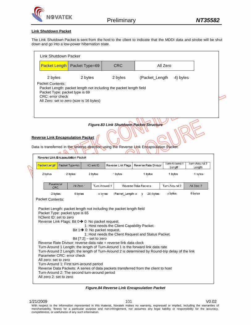
Preliminary NT35582
1/21/2009 101 V0.02 With respect to the information represented in this material, Novatek makes no warranty, expressed or implied, including the warranties of merchantability, fitness for a particular purpose and non-infringement, nor assumes any legal liability or responsibility for the accuracy, completeness, or usefulness of any such information.
Link Shutdown Packet The Link Shutdown Packet is sent from the host to the client to indicate that the MDDI data and strobe will be shut down and go into a low-power hibernation state.
Figure.83 Link Shutdown Packet Structure Reverse Link Encapsulation Packet Data is transferred in the reverse direction using the Reverse Link Encapsulation Packet.
Figure.84 Reverse Link Encapsulation Packet
Packet Contents:
Packet Length: packet length not including the packet length field Packet Type: packet type is 65 hClient ID: set to zero Reverse Link Flags: Bit 0 0: No packet request.
1: Host needs the Client Capability Packet. Bit 1 0: No packet request.
1: Host needs the Client Request and Status Packet. Bit [7:2] – set to zero Reverse Rate Divisor: reverse data rate = reverse link data clock Turn-Around 1 Length: the length of Turn-Around 1 is the forward link data rate Turn-Around 2 Length: the length of Turn-Around 2 is determined by Round-trip delay of the link Parameter CRC: error check All zero: set to zero Turn-Around 1: First turn-around period Reverse Data Packets: A series of data packets transferred from the client to host Turn-Around 2: The second turn-around period All zero 2: set to zero
Link Shutdown Packer
Packet Length Packet Type=69 CRC All Zero
2 bytes 2 bytes 2 bytes (Packet_Length – 4) bytes Packet Contents:
Packet Length: packet length not including the packet length field Packet Type: packet type is 69 CRC: error check All Zero: set to zero (size is 16 bytes)
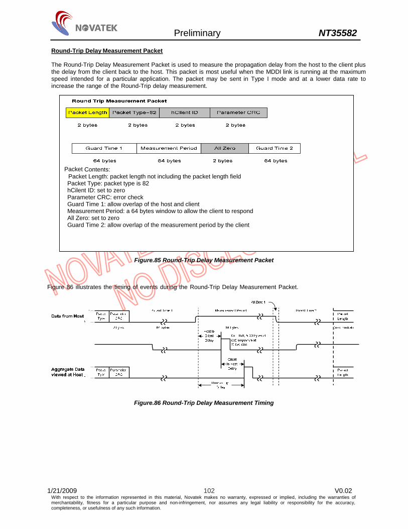
Preliminary NT35582
1/21/2009 102 V0.02 With respect to the information represented in this material, Novatek makes no warranty, expressed or implied, including the warranties of merchantability, fitness for a particular purpose and non-infringement, nor assumes any legal liability or responsibility for the accuracy, completeness, or usefulness of any such information.
Round-Trip Delay Measurement Packet The Round-Trip Delay Measurement Packet is used to measure the propagation delay from the host to the client plus the delay from the client back to the host. This packet is most useful when the MDDI link is running at the maximum speed intended for a particular application. The packet may be sent in Type I mode and at a lower data rate to increase the range of the Round-Trip delay measurement.
Figure.85 Round-Trip Delay Measurement Packet Figure 86 illustrates the timing of events during the Round-Trip Delay Measurement Packet.
Figure.86 Round-Trip Delay Measurement Timing
Packet Contents:
Packet Length: packet length not including the packet length field Packet Type: packet type is 82 hCilent ID: set to zero Parameter CRC: error check Guard Time 1: allow overlap of the host and client Measurement Period: a 64 bytes window to allow the client to respond All Zero: set to zero Guard Time 2: allow overlap of the measurement period by the client
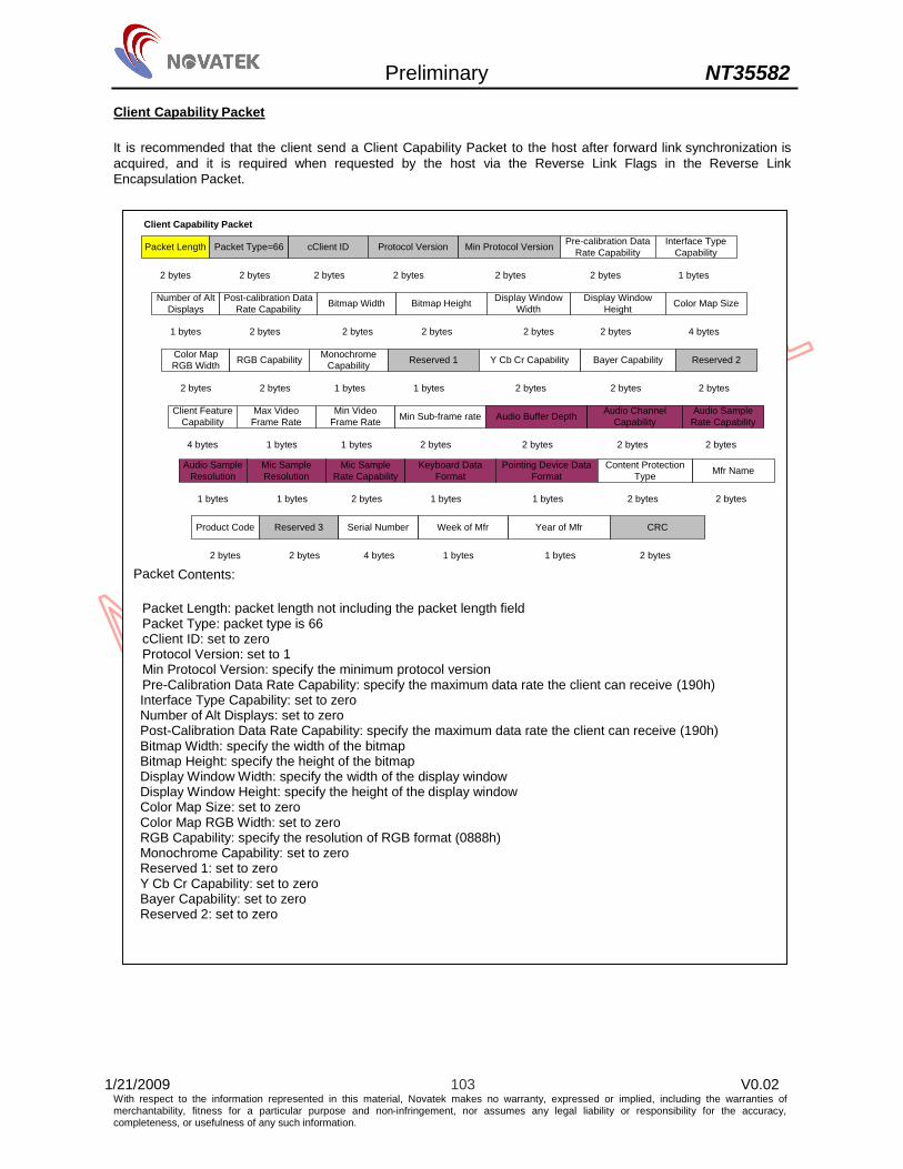
Preliminary NT35582
1/21/2009 103 V0.02 With respect to the information represented in this material, Novatek makes no warranty, expressed or implied, including the warranties of merchantability, fitness for a particular purpose and non-infringement, nor assumes any legal liability or responsibility for the accuracy, completeness, or usefulness of any such information.
Client Capability Packet It is recommended that the client send a Client Capability Packet to the host after forward link synchronization is acquired, and it is required when requested by the host via the Reverse Link Flags in the Reverse Link Encapsulation Packet.
Packet Length Packet Type=66 cClient ID Protocol Version Min Protocol Version Pre-calibration Data Rate Capability
Interface Type Capability
2 bytes 2 bytes 2 bytes 2 bytes2 bytes 2 bytes 1 bytes
Number of Alt Displays
Post-calibration Data Rate Capability Bitmap Width Bitmap Height Display Window
WidthDisplay Window
Height Color Map Size
1 bytes 2 bytes 2 bytes 2 bytes2 bytes 2 bytes 4 bytes
Color Map RGB Width RGB Capability Monochrome
Capability Reserved 1 Y Cb Cr Capability Bayer Capability Reserved 2
2 bytes 2 bytes 1 bytes 2 bytes1 bytes 2 bytes 2 bytes
Client Feature Capability
Max Video Frame Rate
Min Video Frame Rate Min Sub-frame rate Audio Buffer Depth Audio Channel
CapabilityAudio Sample
Rate Capability
4 bytes 1 bytes 1 bytes 2 bytes2 bytes 2 bytes 2 bytes
Audio Sample Resolution
Mic Sample Resolution
Mic Sample Rate Capability
Keyboard Data Format
Pointing Device Data Format
Content Protection Type Mfr Name
1 bytes 1 bytes 2 bytes 1 bytes1 bytes 2 bytes 2 bytes
Product Code Reserved 3 Serial Number Week of Mfr Year of Mfr CRC
2 bytes 2 bytes 4 bytes 1 bytes1 bytes 2 bytes
Client Capability Packet
Packet Contents:
Packet Length: packet length not including the packet length field Packet Type: packet type is 66 cClient ID: set to zero Protocol Version: set to 1 Min Protocol Version: specify the minimum protocol version Pre-Calibration Data Rate Capability: specify the maximum data rate the client can receive (190h) Interface Type Capability: set to zero
Number of Alt Displays: set to zero Post-Calibration Data Rate Capability: specify the maximum data rate the client can receive (190h) Bitmap Width: specify the width of the bitmap Bitmap Height: specify the height of the bitmap Display Window Width: specify the width of the display window Display Window Height: specify the height of the display window Color Map Size: set to zero Color Map RGB Width: set to zero RGB Capability: specify the resolution of RGB format (0888h) Monochrome Capability: set to zero
Reserved 1: set to zero Y Cb Cr Capability: set to zero Bayer Capability: set to zero Reserved 2: set to zero

Preliminary NT35582
1/21/2009 104 V0.02 With respect to the information represented in this material, Novatek makes no warranty, expressed or implied, including the warranties of merchantability, fitness for a particular purpose and non-infringement, nor assumes any legal liability or responsibility for the accuracy, completeness, or usefulness of any such information.
Figure.87 Client Capability Packet
Client Feature Capability Indicators: 00448000h Maximum Video Frame Rate Capability: specify the maximum video frame (3Ch) Minimum Video Frame Rate Capability: specify the minimum video frame (00h) Minimum Sub-frame Rate: specify the minimum sub-frame rate (01h) Audio Buffer Depth: set to zero Audio Channel Capability: set to zero Audio Sample Rate Capability: Set to zero Audio Sample Resolution: set to zero Mic Audio Sample Resolution: set to zero Mic Sample Rate Capability: set to zero Keyboard Data Format: set to zero Pointing Device Data Format: set to zero Content Protection Type: set to zero Mfr Name: set to zero Product Code: set to zero Reserved 3: set to zero Serial Number: set to zero Week of Manufacture: set to zero Year of Manufacture: set to zero
CRC: error check

Preliminary NT35582
1/21/2009 105 V0.02 With respect to the information represented in this material, Novatek makes no warranty, expressed or implied, including the warranties of merchantability, fitness for a particular purpose and non-infringement, nor assumes any legal liability or responsibility for the accuracy, completeness, or usefulness of any such information.
Client Request and Status Packet The host needs a small amount of information from the client so it can configure the host-to-client link in an optimum manner. The Client Request and Status Packet is required to report errors and status to the host.
Figure.88 Client Request and Status Packet
Packet Contents:
Packet Length: packet length not including the packet length field Packet Type: packet type is 70 cClient ID: set to zero Reverse Link Request: specify the number of bytes the client needs in the reverse link in the next sub-frame to send information to the host. CRC Error Count: count the number of CRC errors occurred Client Status:
Bit 0 – Bit 0 = 1- capability has changed = 0 – capability has not changed Bit 1 – indicates the client has detected an error Bit [7:2]: set to zero
Client Busy Flags: Bit 0 – bitmap block transfer function is busy Bit 1 – bitmap area fill function is busy Bit 2 – bitmap pattern fill function is busy Bit 3 – the graphics subsystem is busy Bit [15:4] – set to zero
CRC: error check

Preliminary NT35582
1/21/2009 106 V0.02 With respect to the information represented in this material, Novatek makes no warranty, expressed or implied, including the warranties of merchantability, fitness for a particular purpose and non-infringement, nor assumes any legal liability or responsibility for the accuracy, completeness, or usefulness of any such information.
Register Access Packet Register Access Packet is utilized when setting instruction to the NT35582. This packet cannot be used for RAM access..
Figure.89 Register Access Packet
Register Access Packet
Packet Length Packet Type=146 bClient ID Read/Write
InfoRegisterAddress
ParameterCRC Register Data List
2 bytes 2 bytes 2 bytes 4 bytes2 bytes 2 bytes (Packet Length – 14) bytes
Register Data CRC
2 bytes Packet Contents:
Packet Length: packet length not including the packet length field Packet Type: packet type is 146 bClient ID: set to zero Read/Write Info:
Bits [15:14] Read/Write Flags 00 Write 01 Reserved 10 Read 11 Response to read
Bit [13:0] – specifies the number of 32-bit register data list items to be transferred in the Register Data
List Filed. Register Address: upper bits shall set to zero Parameter CRC: error check from packet length to the register address Register Data List: written (or read) registers to (from) client Register Data CRC: error check of the register data list

Preliminary NT35582
1/21/2009 107 V0.02 With respect to the information represented in this material, Novatek makes no warranty, expressed or implied, including the warranties of merchantability, fitness for a particular purpose and non-infringement, nor assumes any legal liability or responsibility for the accuracy, completeness, or usefulness of any such information.
Video Stream Packet The NT35582 supports the Video Stream Packet to transfer display data including RGB data to RAM.
Figure.90 Video Stream Packet
Packet Contents:
Packet Length: packet length not including the packet length field Packet Type: packet type is 16
bClient ID: set to zero Pixel Data Attributes: set to zero Video Data Format Descriptor: refer Table 5.6.4 X Left Edge: Specify the X coordinate of the left edge of the screen window filled by the Pixel Data field. Y Top Edge: Specify the Y coordinate of the top edge of the screen window filled by the Pixel Data field X Right Edge: Specify the X coordinate of the right edge of the window being updated. Y Bottom Edge: Specify the Y coordinate of the bottom edge of the window being updated. X Start: Specify X start address for the first pixel in the Pixel Data field below. Y Start: Specify Y start address for the first pixel in the Pixel Data field below Pixel Count: specify the number of pixels Parameter CRC: error check from packet length to the pixel count Pixel Data: the raw video data Pixel Data CRC: error check of the pixel data
Table 5.7.2 Video data format descriptor [15:12] [11:8] [7:4] [3:0] Transfer pixel format
0101 0x8 0x8 0x8 Packed 24 bits pixel RGB format (R:G:B=8:8:8)
0101 0x6 0x6 0x6 Packed 18 bits pixel RGB format (R:G:B=6:6:6)
0101 0x5 0x6 0x5 Packed 16 bits pixel RGB format (R:G:B=5:6:5)
Others setting disabled
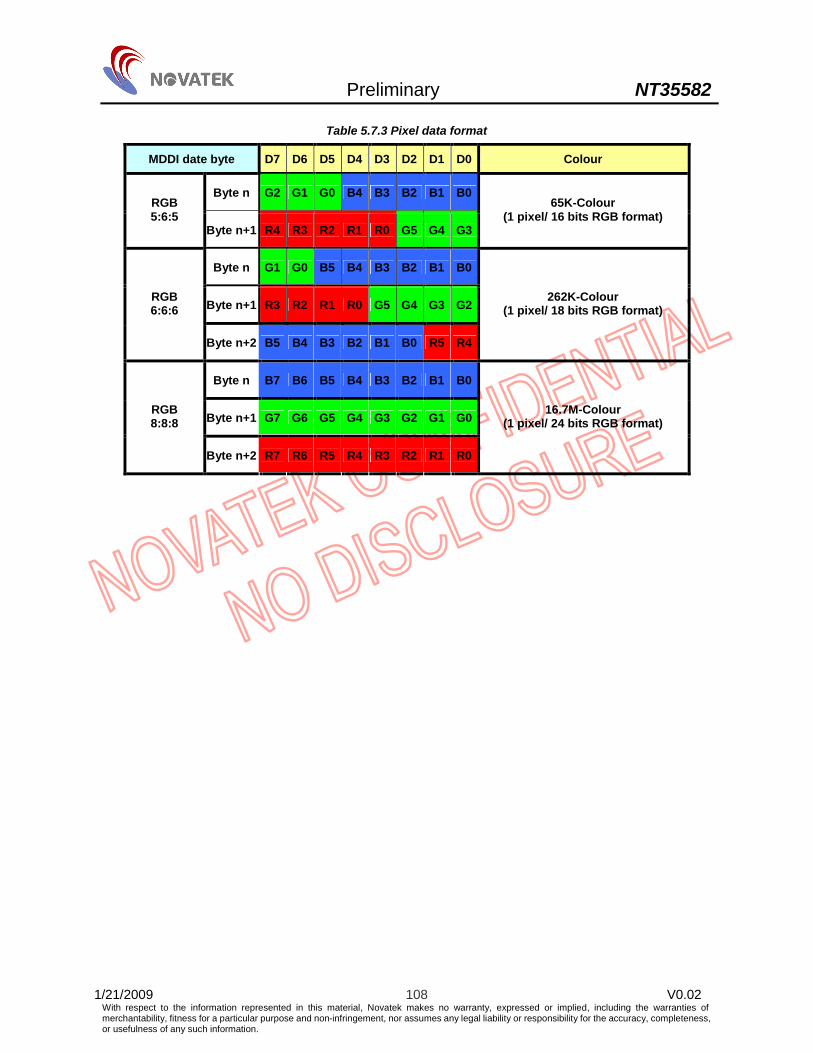
Preliminary NT35582
1/21/2009 108 V0.02 With respect to the information represented in this material, Novatek makes no warranty, expressed or implied, including the warranties of merchantability, fitness for a particular purpose and non-infringement, nor assumes any legal liability or responsibility for the accuracy, completeness, or usefulness of any such information.
Table 5.7.3 Pixel data format
MDDI date byte D7 D6 D5 D4 D3 D2 D1 D0 Colour
Byte n G2 G1 G0 B4 B3 B2 B1 B0 RGB 5:6:5
Byte n+1 R4 R3 R2 R1 R0 G5 G4 G3
65K-Colour (1 pixel/ 16 bits RGB format)
Byte n G1 G0 B5 B4 B3 B2 B1 B0
Byte n+1 R3 R2 R1 R0 G5 G4 G3 G2 RGB 6:6:6
Byte n+2 B5 B4 B3 B2 B1 B0 R5 R4
262K-Colour (1 pixel/ 18 bits RGB format)
Byte n B7 B6 B5 B4 B3 B2 B1 B0
Byte n+1 G7 G6 G5 G4 G3 G2 G1 G0 RGB 8:8:8
Byte n+2 R7 R6 R5 R4 R3 R2 R1 R0
16.7M-Colour (1 pixel/ 24 bits RGB format)

Preliminary NT35582
1/21/2009 109 V0.02 With respect to the information represented in this material, Novatek makes no warranty, expressed or implied, including the warranties of merchantability, fitness for a particular purpose and non-infringement, nor assumes any legal liability or responsibility for the accuracy, completeness, or usefulness of any such information.
5.7.3 Writing Video Data to Memory Sequence In order to write video data to memory, the following sequence should be programmed. This packet should be followed by video stream packets.
Video Data Transfer(Video Stream Packet)
Video Data Transfer(Video Stream Packet)
Video Data Transfer(Video Stream Packet)
Figure.91 Writing video data to memory sequence
5.7.4 Writing Register Sequence In order to write registers, register access packet should be used. Register access packet is used to write data to register.
Command Transfer( Register Access packet )
Figure.92 Writing register sequence

Preliminary NT35582
1/21/2009 110 V0.02 With respect to the information represented in this material, Novatek makes no warranty, expressed or implied, including the warranties of merchantability, fitness for a particular purpose and non-infringement, nor assumes any legal liability or responsibility for the accuracy, completeness, or usefulness of any such information.
5.7.5 Reading Video Data from Memory Sequence In order to read a pixel data from memory (readable one pixel only), the following sequence should be programmed. Memory read command (2E00h) is followed by reverse encapsulation packet. DDI transmits video pixel data through encapsulation packet. Please refer to VESA spec for detailed description.
Round Trip Delay Measurement Transfer( Round Trip Delay Measurement Packet)
Read Memory(02E0h)Transfer(Register Access Packet)
Reverse Encapsulation Transfer(Reverse Encapsulation Packet)
Figure.93 Reading video data from memory sequence
5.7.6 Reading Register Sequence In order to read registers, the following sequence should be programmed. Next, register read command is followed by reverse encapsulation packet. DDI transmits register data through encapsulation packet. Please refer to VESA spec for detailed description.
Figure.94 Reading register sequence
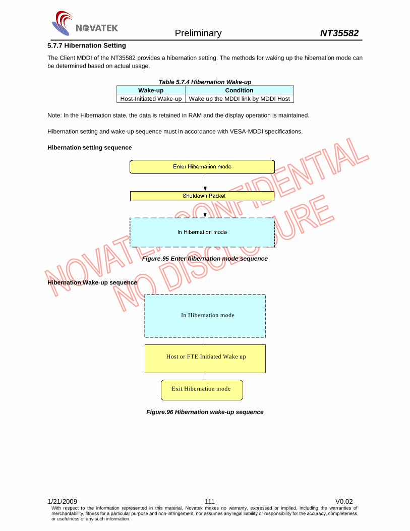
Preliminary NT35582
1/21/2009 111 V0.02 With respect to the information represented in this material, Novatek makes no warranty, expressed or implied, including the warranties of merchantability, fitness for a particular purpose and non-infringement, nor assumes any legal liability or responsibility for the accuracy, completeness, or usefulness of any such information.
5.7.7 Hibernation Setting
The Client MDDI of the NT35582 provides a hibernation setting. The methods for waking up the hibernation mode can be determined based on actual usage.
Table 5.7.4 Hibernation Wake-up Wake-up Condition
Host-Initiated Wake-up Wake up the MDDI link by MDDI Host Note: In the Hibernation state, the data is retained in RAM and the display operation is maintained. Hibernation setting and wake-up sequence must in accordance with VESA-MDDI specifications. Hibernation setting sequence
Figure.95 Enter hibernation mode sequence Hibernation Wake-up sequence
In Hibernation mode
Host or FTE Initiated Wake up
Exit Hibernation mode
Figure.96 Hibernation wake-up sequence
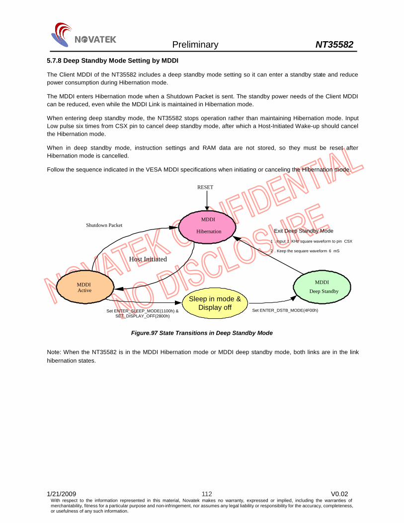
Preliminary NT35582
1/21/2009 112 V0.02 With respect to the information represented in this material, Novatek makes no warranty, expressed or implied, including the warranties of merchantability, fitness for a particular purpose and non-infringement, nor assumes any legal liability or responsibility for the accuracy, completeness, or usefulness of any such information.
5.7.8 Deep Standby Mode Setting by MDDI
The Client MDDI of the NT35582 includes a deep standby mode setting so it can enter a standby state and reduce power consumption during Hibernation mode.
The MDDI enters Hibernation mode when a Shutdown Packet is sent. The standby power needs of the Client MDDI can be reduced, even while the MDDI Link is maintained in Hibernation mode.
When entering deep standby mode, the NT35582 stops operation rather than maintaining Hibernation mode. Input Low pulse six times from CSX pin to cancel deep standby mode, after which a Host-Initiated Wake-up should cancel the Hibernation mode.
When in deep standby mode, instruction settings and RAM data are not stored, so they must be reset after Hibernation mode is cancelled.
Follow the sequence indicated in the VESA MDDI specifications when initiating or canceling the Hibernation mode.
Deep Standby
MDDI
Hibernation
MDDIActive
Shutdown Packet
RESET
Host Initiated
MDDI
Exit Deep Standby Mode
1 .
2 .
Sleep in mode & Display off Set ENTER_DSTB_MODE(4F00h)
Keep the sequare waveform 6 mS
Input 1 KHz square waveform to pin CSX
Set ENTER_SLEEP_MODE(1100h) & SET_DISPLAY_OFF(2800h)
Figure.97 State Transitions in Deep Standby Mode
Note: When the NT35582 is in the MDDI Hibernation mode or MDDI deep standby mode, both links are in the link hibernation states.

Preliminary NT35582
1/21/2009 113 V0.02 With respect to the information represented in this material, Novatek makes no warranty, expressed or implied, including the warranties of merchantability, fitness for a particular purpose and non-infringement, nor assumes any legal liability or responsibility for the accuracy, completeness, or usefulness of any such information.
Deep standby Mode Sequence
Deep standby mode
Host - Initiated Wake up
Set ENTER_DSTB_MODE(4F00h) (Register Access Packet)
Exit deep standby mode
2. Keep the sequare waveform 6ms
Initial instruction setting RAM data setting
Display on sequence
Enter Sleep In Mode & Display Off
1. 1KHz square waveform to pin CSX
Figure.98 Enter and Exit deep standby mode sequence Note: When in deep standby mode, instruction settings and RAM data are not stored, so they must be reset after Hibernation mode is cancelled.

Preliminary NT35582
1/21/2009 114 V0.02 With respect to the information represented in this material, Novatek makes no warranty, expressed or implied, including the warranties of merchantability, fitness for a particular purpose and non-infringement, nor assumes any legal liability or responsibility for the accuracy, completeness, or usefulness of any such information.
5.8 High-Speed RAM Write Function The difference between normal RAM write and high-speed RAM write is that the minimum window address area is limited (refer to RAM write operation). In high-speed RAM write mode (HSM=1), the data is buffered in the internal register of the NT35582. Two pixel data will be collected in internal register and transferred to the internal RAM at the same time. When transferring the data from the internal register to the internal RAM, the data for the next two pixels can be transferred to the internal buffer.
CSX
WRX
Data Businput
Index(2C0) (2)
RAM data
(1) (2)(1)Index(2C0)
Figure.99 Example of High-Speed RAM Write Operation (HSM = 1)
Remark: When switching from high-speed RAM write operation to index write operation, a minimum of two normal RAM write bus cycle periods (2 x tWC) should occur before the next instruction is performed. Notes 1. If Index is set to 2C00h and HSM = “1”, RAM write operation will be executed, but RAM read operation will not occur.
Ensure that HSM = 0 before executing RAM read operation. 2. This function cannot be used when writing data in normal RAM write mode. When switching from one write mode to
the other, write operation should begin only after switching modes and setting RAM address (XAD[9:0], YAD[9:0]). 3. In high-speed mode, No resizing function.
Table 5.8.1 Different between normal RAM write and High Speed RAM write Operation RAM read RAM write Window address MV
Normal RAM Write (HSM = 0) In units of pixel In units of pixel In units of pixel MV = 1/0
High-speed RAM Write (HSM = 1) Not available In units of two
pixel
In units of pixel (minimum window address area :
32 pixels x 1 line) MV = 0

Preliminary NT35582
1/21/2009 115 V0.02 With respect to the information represented in this material, Novatek makes no warranty, expressed or implied, including the warranties of merchantability, fitness for a particular purpose and non-infringement, nor assumes any legal liability or responsibility for the accuracy, completeness, or usefulness of any such information.
5.8.1 High-Speed RAM Data Write in Window Address Area
The NT35582 is able to execute consecutive high-speed data rewrite operations within a rectangular area (minimum size of 8 words x 1 line). This area is determined in the internal RAM using settings below.
If the high-speed RAM write function is used to write data to the internal RAM, ensure that each line of the window address area is overwritten at the same time. Set the write start address in the start address of the window address area. If the data buffered in the NT35582’s internal register is not written from the start of a line, or is insufficient to rewrite the horizontal line of the window address area, the data is not rewritten on the RAM data in the line.
GRAM address
Re- write area
XSA, YSA
XEA , YEA
XAD = 000hYAD = 000h
XAD = 1DFhYAD = 31Fh
High speed RAM write sequence1 . Set MV = 02 . Set GRAM re-write area ( XSA, XEA,YSA, YEA)3 . Enable high speed mode ( Set HSM = 1)4 . Setting RAM address within the re-write area (Set AD)5 . GRAM write ( XEA-XSA+1)*(YEA-YSA+1) times
Figure.100 High-Speed RAM write operation in the window address area

Preliminary NT35582
1/21/2009 116 V0.02 With respect to the information represented in this material, Novatek makes no warranty, expressed or implied, including the warranties of merchantability, fitness for a particular purpose and non-infringement, nor assumes any legal liability or responsibility for the accuracy, completeness, or usefulness of any such information.
5.9 Window Address Function
The window address function allows writing RAM data consecutively within the window address area which are determined by setting the horizontal address register (XSA and HEA) and vertical address register (YSA and YEA). The MV, MX and MY bits determine the transition direction of the RAM address (refer to register 3600h ).
The RAM address (XAD[9:0], YAD[9:0]) must be set within the window address area, and the window address must be made within the GRAM address map area.
Example: 480RGBx864 resolution [Window Address area setting range]:
(Horizontal direction) 10h000 ≤ XSA ≤ XEA ≤ 10h1DF (Vertical direction) 10’h000 ≤ YSA ≤ YEA ≤ 10h35F
[RAM Address setting range]:
(RAM address) XSA ≤ XAD[9:0] ≤ XEA YSA ≤ YAD[9:0] ≤ YEA

Preliminary NT35582
1/21/2009 117 V0.02 With respect to the information represented in this material, Novatek makes no warranty, expressed or implied, including the warranties of merchantability, fitness for a particular purpose and non-infringement, nor assumes any legal liability or responsibility for the accuracy, completeness, or usefulness of any such information.
5.10 Reduced Power Consumption Drive Settings
The NT35582 supports various methods for reducing power consumption. Generally speaking, a balance will need to be found between reduced power consumption and display quality. In addition, the power consumption also depends on the characteristics of the panel. Review the various methods to determine which one will provide the optimal balance between reduced power consumption and display quality.
Frame Rate Setting The NT35582 is able to change the liquid crystal polarity inversion cycle by setting the DIV, RTN bits to change the frame frequency. Setting a lower frequency in the partial display operation will reduce power consumption. For more information, refer to “Frame-Frequency Adjustment Frequency.”
5.11 ZigZag, Column, 1-Dot, 2-Dot Inversion (VCOM DC Drive) The NT35582, in addition to the frame-inversion liquid crystal drive, supports the ZigZag, column, 1–dot and 2-dot inversion driving methods to invert the polarity of liquid crystal. The ZigZag, column, 1–dot and 2-dot inversion can provide a solution for improving display quality. In determining the inversion drive for the inversion cycle, check the quality of display on the liquid crystal panel. Note that setting 1-dot inversion will raise the frequency of the liquid crystal polarity inversion and increase the charging/discharging current on liquid crystal cells.

Preliminary NT35582
1/21/2009 118 V0.02 With respect to the information represented in this material, Novatek makes no warranty, expressed or implied, including the warranties of merchantability, fitness for a particular purpose and non-infringement, nor assumes any legal liability or responsibility for the accuracy, completeness, or usefulness of any such information.
5.12 Frame Frequency Adjustment Function
The NT35582 provides a function to adjust the frame frequency for driving liquid crystal by setting the T2 and VPA register without changing the oscillation frequency.
Changing the frame frequency is permissible when a moving picture or still picture is displayed on the screen; a high oscillation frequency should be set in this case. By changing the VPA and T2 settings, the NT35582 can function at a low frame frequency to display a still picture (reducing power consumption), and at a high frame frequency when displaying a moving picture (which requires data to be rewritten at high speed).
Relationship between Liquid Crystal Drive Duty and the Frame Frequency
The formula below is used to calculate the relationship between the liquid crystal drive duty and the frame frequency. The frame frequency is determined by setting the 1-line period adjustment T2 register and the operation blank line by VPA register.
Equation for calculating frame frequency is as below.
Frame frequency
= (Hz)
T(1Line) : Line
Display line time (setting by T2 register)
VPA Number of lines for porch
( T(1Line) x ( Line+VPA[7:0])1
: Number of Display line :

Preliminary NT35582
1/21/2009 119 V0.02 With respect to the information represented in this material, Novatek makes no warranty, expressed or implied, including the warranties of merchantability, fitness for a particular purpose and non-infringement, nor assumes any legal liability or responsibility for the accuracy, completeness, or usefulness of any such information.
5.13 GAMMA CORRECTION FUNCTION The structure of grayscale amplifier is shown as below. The 13 voltage levels between VGMP/VGMN and VGSP/VGSN are determined by the gradient adjustment register, the reference adjustment register, the amplitude adjustment resister and the micro-adjustment register.
R
Rx127
V0
V1DAC
128 to 1
V127V0
DAC64 to 1
DAC128 to 1
DAC128 to 1
R
R
R
R
V95
V96V0
DAC64 to 1
V126
R
V127
DAC128 to 1
DAC128 to 1
DAC128 to 1
V80
V8
V175
V247
V0~V127
V0~V127
V0~V127
V3~V66
V33~V96
V0~V127
V0~V127
V239V0~V127
V16
V24
V52
V108
V147
V203
V231
R
R
V0
V1
DAC128 to 1
V0-V 127
V 255
DAC128 to 1
DAC256 to 1
R
R
R
R
V 256
V 257
V 510DAC
128 to 1V384- V 511
DAC256 to 1
V256- V 511
DAC128 to 1
V 384- V 511R
R
V 511
DAC256 to 1
V 128-V 383
DAC256 to 1
V190-V 445
DAC256 to 1
V10 - V 265
DAC256 to 1
V246-V 501
V0
V1
V255
V254
V4
V8
V80
V175
V247
V251
V0-V127
V0-V127
V0-V127
V0-V127
V0-V127
V0-V127
V3-V66
V33-V96
V0-V127
V0-V255
VGMP (VGMN)
VGSP (VGSN)
Rx127
Rx96Rx511
Figure.101 The structure of gamma correction

Preliminary NT35582
1/21/2009 120 V0.02 With respect to the information represented in this material, Novatek makes no warranty, expressed or implied, including the warranties of merchantability, fitness for a particular purpose and non-infringement, nor assumes any legal liability or responsibility for the accuracy, completeness, or usefulness of any such information.
5.14 Reset Function The RESET function of NT35582 is triggered by a RESET input. After reset function triggered, the NT35582 enters a reset period, and the duration of this period must be at least 1ms. During this period, the NT35582 and its power circuit is initialized. In the meanwhile, because the NT35582 will be in a busy state, neither instruction from MPU nor GRAM data access request are not acceptable. In addition, for power-on reset case, there will be a 2ms period for oscillator to be stable. Therefore, any instructions or GRAM access request must be made after this 2ms period is over. 1. Initial states of output pins The following table represents the output pins and its initial state.
Output Pins Initial State Liquid crystal driver (Source driver output) All output VSS
VCOM Disabled (VSS level output)
VGMP Disabled (VSS level output)
VGMN Disabled (VSS level output)
VGSP Disabled (VSS level output)
VGSN Disabled (VSS level output)
AVDD VCI
AVEE Disabled (VSS level output)
NVDD Disabled (VSS level output)
VREF1 Disabled (VSS level output)
VREF2 Disabled (VSS level output)
SOUT1-18 Disabled (VSS level output)
FTE Disabled (VSS level output)
High(= VDDI): When IM = 3’b001 (Serial Interface) SDO
Disabled (VSS level output)
D23-0,SDI Hi-z
VGH VCI
VGL VSS
VGHO VSS
VCL VSS
2. Initial states of input/output pins The following table represents the input/output pins and its initial state.
Input/Output Pins Initial State
CxP (C11P~C14P, C21P~C24P, C31P~C32P, C41P~C42P) VCI
CxM (C11M~C14M, C21M~C24M, C31M~C32M, C41M~C42M) VSS
Note: The initial states of input/output pins listed above are proper under the condition that LCD module is connected as shown in the connection example.
Preliminary NT35582
1/21/2009 121 V0.02 With respect to the information represented in this material, Novatek makes no warranty, expressed or implied, including the warranties of merchantability, fitness for a particular purpose and non-infringement, nor assumes any legal liability or responsibility for the accuracy, completeness, or usefulness of any such information.
3. Initial state of instruction set The initial state of instruction set is listed in next chapter, and the default values are shown in the parenthesis of each instruction bit cell. 4. Initial state of RAM data The data in RAM is not automatically initialized in RESET period, and must be initialized by software before display-on instruction is made. 5. Note on Reset function (a) When NT35582 is in deep standby mode, the logic regulator will start and make a transition to initial state if
a RESET signal is inputted. In this situation, the interface pins are possible placed in unstable conditions. To avoid this situation happening, DO NOT send a RESET signal when NT35582 is in deep standby mode.
(b) Ensure to execute data transfer synchronization after executing a RESET when transferring instruction in either two or three transfer mode via 8-/16/24-bit interface.

Preliminary NT35582
1/21/2009 122 V0.02 With respect to the information represented in this material, Novatek makes no warranty, expressed or implied, including the warranties of merchantability, fitness for a particular purpose and non-infringement, nor assumes any legal liability or responsibility for the accuracy, completeness, or usefulness of any such information.
5.15 Basic Operation Mode The basic operation mode of NT35582 is illustrated below. When changing from one mode to another, make sure to follow the sequence indicated in the figure.
Exit Sleep m
ode
Enter Sleep mode
Set Display O
n
Set Display O
ff
Figure.102 The basic operation mode of NT35582

Preliminary NT35582
1/21/2009 123 V0.02 With respect to the information represented in this material, Novatek makes no warranty, expressed or implied, including the warranties of merchantability, fitness for a particular purpose and non-infringement, nor assumes any legal liability or responsibility for the accuracy, completeness, or usefulness of any such information.
5.16 Power Supply Setting Sequence The power supply ON/OFF setting for Display ON/OFF, Standby Set/Exit, and Sleep Set/Exit sequences is illustrated in the figure below.
Power ON Sequence
Hardware reset
Sleep out commandSet EXIT_ SLEEP_ MODE
( 1100h)
20 ms or more
Display on commandSet SET_ DISPLAY_ ON
( 2900h)
120 ms or more
Power OFF Sequence
Display off commandSet SET_ DISPLAY_ OFF
( 2800h)
Sleep in commandSet ENT_ SLEEP_ MODE
( 1000h)
3 frames or more
Power Supply ON
Normal Display
Normal Display
Power Supply OFF
Figure.103 Power supply On / Off setting sequence
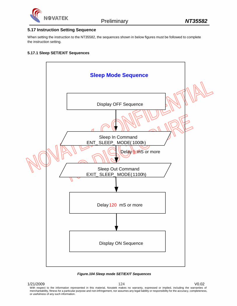
Preliminary NT35582
1/21/2009 124 V0.02 With respect to the information represented in this material, Novatek makes no warranty, expressed or implied, including the warranties of merchantability, fitness for a particular purpose and non-infringement, nor assumes any legal liability or responsibility for the accuracy, completeness, or usefulness of any such information.
5.17 Instruction Setting Sequence When setting the instruction to the NT35582, the sequences shown in below figures must be followed to complete the instruction setting.
5.17.1 Sleep SET/EXIT Sequences
Sleep Mode Sequence
Sleep In CommandENT_ SLEEP_ MODE ( 1000h)
Sleep Out CommandEXIT_ SLEEP_ MODE (1100h)
Display ON Sequence
Display OFF Sequence
Delay 120 mS or more
Delay 5 mS or more
Figure.104 Sleep mode SET/EXIT Sequences

Preliminary NT35582
1/21/2009 125 V0.02 With respect to the information represented in this material, Novatek makes no warranty, expressed or implied, including the warranties of merchantability, fitness for a particular purpose and non-infringement, nor assumes any legal liability or responsibility for the accuracy, completeness, or usefulness of any such information.
5.17.2 Deep Standby Mode SET/EXIT Sequences
Into Deep Standby ModeENTER_DSTB_MODE(4F00h), and set DSTB = 1
Initial instruction setting RAM data setting
Display on sequence
Deep standby mode Enter /EXIT Sequence
Exit deep standby mode
1 . Input 1 KHz square waveform to pin CSX
2 . Keep the sequare waveform 6mS
Into Sleep In Mode
Set display off (2800h)
Or set RESET to exit deep standby mode
a.
b.
Set ENTER _SLEEP _MODE(1000 h)
Delay 5ms
Figure.105 Deep Standby Mode SET/EXIT Sequences

Preliminary NT35582
1/21/2009 126 V0.02 With respect to the information represented in this material, Novatek makes no warranty, expressed or implied, including the warranties of merchantability, fitness for a particular purpose and non-infringement, nor assumes any legal liability or responsibility for the accuracy, completeness, or usefulness of any such information.
5.18 NVM Write Sequence
* Adjust Voltage Level VCOM VM[7 0] (C700h) * Write : ID[6 0] (1280h)*Power on and normal display
Check 0x1C80 == 0x83 (if 1st write ID and VCOM)
Write 0xF800= 0x80 for OTP Write Enable
EPWRITE Write 0x1D80 = 0x55Write 0x1E80 = 0xAAWrite 0x1F80 = 0x66Wait for 100ms
Remove input power from MTP- PWR pin
H/W ResetCheck ID and VCOM value
Read data all correct No
execute EPWRITE FlowRe-
Yes
START
MTP-PWR pin connect
END
Figure.106 NVM write sequences

Preliminary NT35582
1/21/2009 127 V0.02 With respect to the information represented in this material, Novatek makes no warranty, expressed or implied, including the warranties of merchantability, fitness for a particular purpose and non-infringement, nor assumes any legal liability or responsibility for the accuracy, completeness, or usefulness of any such information.
5.19 Instruction Setup Flow
5.19.1 Initializing with the Build-in Power Supply Circuit
H/ W Reset‧ Power Input : VDDI and VCI ( VDDAM)
Wait Until Power Stabilization‧ RESX = "L"
Wait for more than 10 ms‧
Power Supply Set‧ EXIT_SLEEP_MODE (Sleep mode OFF & OSC / Booster ON )
Display Environment Set ( If not used, can be skipped )
‧
‧
‧‧
‧
‧
‧
‧
‧
‧
Display Data Write & Display On‧
‧
‧
Initializing End
Initializing Start ( Power ON )
RESX = "L"
SET_COLUMN_ADDRESS / SET_ROW_ADDRESS ( Row / Column Address Set ) Start / End row address set (YS, YE) and Start / End column address set (XS, XE)WRITE_MEMORY_START ( Memory Data Write )Wait for more than 120 mS after power control commandSET_DISPLAY_ON ( Display ON )
ENTER_INVERT_MODE / EXIT_INVERT_MODE ( Display Inversion / Normal Set )ENTER_IDLE_MODE / EXIT_IDLE_MODE ( Idle Mode On / Off )ENTER_PARTIAL_MODE / EXIT_PARTIAL_MODE ( Partial Mode On / Off )SET_PARTIAL_AREA ( Partial area set ) Partial start / end line set ( PSL, PEL )SET_ADDRESS_MODE ( Memory Data Access Control ) Row direction (MY), Column direction (MX), Address direction (MV), Scan direction (ML) and RGB orderSET_PIXEL_FORMAT ( Interface Pixel Format Set )SET_GAMMA_CURVE ( Gamma 1.0, 1.8, 2.2, 2.5 curve select )SET_TEAR_ON / SET_TEAR_OFF ( Tearing effect function On / Off )SET_TEAR_SCANLINE ( Set the FTE output position )If CABC / LABC is enable, set related commands ( ex. WRDISBV… etc. )
Figure.107 Power On sequences

Preliminary NT35582
1/21/2009 128 V0.02 With respect to the information represented in this material, Novatek makes no warranty, expressed or implied, including the warranties of merchantability, fitness for a particular purpose and non-infringement, nor assumes any legal liability or responsibility for the accuracy, completeness, or usefulness of any such information.
5.19.2 Power Off Sequence
‧
Power OFF Start ( Without H/W Reset )
‧
Power OFF End
‧
‧
Power OFF End
SET_DISPLAY_OFF ( Display Off )All of the common & segment pins become VC potentialBlanking display ( white for NW display and black for NB display )
ENTER_SLEEP_MODE ( Sleep In )All the liquid crystal power supply circuits and oscillator circuit become Off
Wait for more than 50 mS
Stop the power supply: VCI, VDDI and VDDAM stop (any order)
‧
‧
Power OFF Start ( With H/W Reset )
Wait for more than 50 mS
Stop the power supply: VCI, VDDI and VDDAM stop (any order)
‧
‧
RESX = "L"Wait for more than 5 mSRESX = "H"
Figure.108 Power Off sequences

Preliminary NT35582
1/21/2009 129 V0.02 With respect to the information represented in this material, Novatek makes no warranty, expressed or implied, including the warranties of merchantability, fitness for a particular purpose and non-infringement, nor assumes any legal liability or responsibility for the accuracy, completeness, or usefulness of any such information.
5.20 Power Block
C11
C12
C13
C14
`
AVDDCS1
C21
C22
C23
C24
AVEECS2
C31
C32
VCLCS3
CS4
C41
CS5
C51
VGH
VGL
VGSP
VGMP
VGSN
VGMN
VCOM
D1
Driver IC
VCI, VDDAM
VDDI
CS6
CS7CS8CS9
CS10CS11
CS12
CS13
(5.8~6.5V)
(1.65~3.3V)
(2.5~3.3V)
(5.8 ~ 6.5V)
(2.5 ~ 3.3V)
(2.0 ~ 2.0V)
(2.92 ~ 6.288V)
(2.92 ~ 6.288V)
(7.5 ~ 15V)
(7.5 ~ 15V)
(0 ~ 3.728V)
(0 ~ 3.728V)
Figure.109 Power bolck

Preliminary NT35582
1/21/2009 130 V0.02 With respect to the information represented in this material, Novatek makes no warranty, expressed or implied, including the warranties of merchantability, fitness for a particular purpose and non-infringement, nor assumes any legal liability or responsibility for the accuracy, completeness, or usefulness of any such information.
5.21 Maximum Series Resistance The driver will operate in “Chip on Glass” applications with series resistances (due to ITO track resistance). Voltages are specified at module I/O assuming maximum values as in Table 7.5.1.
Table 7.5.1 Maximum series resistance on module
Name Type Maximum Series Resistance Unit
VDDI Power supply 20 Ω
VCI, VDDAM Power supply 5 Ω
VSS Power supply 10 Ω
VG_MDDI Power supply 10 Ω
CVSS, AVSS,AVSSR Power supply 5 Ω GM[2:0], IM[3:0], PNL, FRM, NBWSEL, TB, RL, SHUT Input 100 Ω
SA[1:0] Input 100 Ω RESX Input 100 Ω
WRX, RDX, DCX, CSX Input 50 Ω
SDI, SDO Input / Output 50 Ω
D23 to D0 Input 50 Ω
PCLK, DE, VS, HS Input 50 Ω FTE Output 50 Ω LED_PWM, LED_ON Output 50 Ω
MDDI_DATA_P, MDDI_DATA_N Input 10 Ω
MDDI_STB_P, MDDI_STB_N Input 10 Ω
VCC, NVDD Capacitor connection 10 Ω
VP_MDDI Capacitor connection 5 Ω
VREF, CAMP_REF Capacitor connection 10 Ω
C11P/N~C14P/N Capacitor connection 5 Ω
C21P/N~C24P/N Capacitor connection 5 Ω
C31P/N~C32P/N Capacitor connection 5 Ω
C41P/N, C51P/N Capacitor connection 10 Ω
AVDD, AVEE, VCL Capacitor connection 5 Ω
VGH, VGL Capacitor connection 10 Ω
VCOM Capacitor connection 5 Ω
VGMP, VGSP, VGMN, VGSN Output 20 Ω
TA1, TA2 Output 20 Ω STV, CLK, XCLK, U2D, D2U, SW1~SW3, CTRL1~CTRL6 Output 50 Ω
MTP_PWR Power supply 15 Ω

Preliminary NT35582
1/21/2009 131 V0.02 With respect to the information represented in this material, Novatek makes no warranty, expressed or implied, including the warranties of merchantability, fitness for a particular purpose and non-infringement, nor assumes any legal liability or responsibility for the accuracy, completeness, or usefulness of any such information.
5.22 External Components Connection
Pad Name Connection Typical Value
VDDI Interface Power VDDI ------||------ GND 1.0μF (Max 6V) VCI (VDDAM) DC-DC, Analog and Regulator Power VCI ------||------ GND 4.7μF (Max 6V) VSS, CVSS, AVSS, AVSSR
Connect to GND
VG_MDDI Connect to GND VCC Connect to Capacitor (Max 6V): VCC ------||------ GND 2.2μF (Max 6V) NVDD Connect to Capacitor (Max 6V): NVDD ------||------ GND 1.0μF (Max 6V) VP_MDDI Connect to Capacitor (Max 6V): VP_MDDI ------||------ GND 2.2μF (Max 6V) VREF Connect to Capacitor (Max 6V): VREF ------||------ GND 1.0μF (Max 6V) CAMP_REF Connect to Capacitor (Max 6V): VREF ------||------ GND 1.0μF (Max 6V) C11P, C11N Connect to Capacitor (Max 6V): C11P ------||------ C11N 1.0μF (Max 6V) C12P, C12N Connect to Capacitor (Max 10V): C12P ------||------ C12N 1.0μF (Max 10V) C13P, C13N Connect to Capacitor (Max 6V): C13P ------||------ C13N 1.0μF (Max 6V) C14P, C14N Connect to Capacitor (Max 10V): C14P ------||------ C14N 1.0μF (Max 10V) C21P, C21N Connect to Capacitor (Max 10V): C21P ------||------ C21N 1.0μF (Max 10V) C22P, C22N Connect to Capacitor (Max 16V): C22P ------||------ C22N 1.0μF (Max 16V) C23P, C23N Connect to Capacitor (Max 10V): C23P ------||------ C23N 1.0μF (Max 10V) C24P, C24N Connect to Capacitor (Max 16V): C24P ------||------ C24N 1.0μF (Max 16V) C31P, C31N Connect to Capacitor (Max 6V): C31P ------||------ C31N 1.0μF (Max 6V) C32P, C32N Connect to Capacitor (Max 6V): C32P ------||------ C32N 1.0μF (Max 6V) C41P, C41N Connect to Capacitor (Max 16V): C41P ------||------ C41N 1.0μF (Max 16V) C51P, C51N Connect to Capacitor (Max 16V): C51P ------||------ C51N 1.0μF (Max 16V) AVDD Connect to Capacitor (Max 10V): AVDD ------||------ GND 4.7μF (Max 10V) AVEE Connect to Capacitor (Max 10V): AVEE ------||------ GND 4.7μF (Max 10V) VCL Connect to Capacitor (Max 6V): VCL ------||------ GND 2.2μF (Max 6V) VGH Connect to Capacitor (Max 16V): VGH ------||------ GND 1.0μF (Max 16V)
VGL Connect to Capacitor (Max 16V): VGL ------||------ GND Connect to Diode: VGL -----|----- GND
1.0μF (Max 16V)
VCOM Connect to Capacitor (Max 6V): VCOM ------||------ GND 2.2μF (Max 6V) MDDI_DATA_P MDDI_DATA_N
Connect to Resistor (2%): MDDI_DATA_P ----WW---- MDDI_DATA_N 100Ω (2%)
MDDI_DATA_P MDDI_DATA_N
Connect to Resistor (2%): MDDI_STB_P ----WW---- MDDI_STB_N 100Ω (2%)
Note: Schottky Diode: VF<0.4V at 20mA, VR>30V
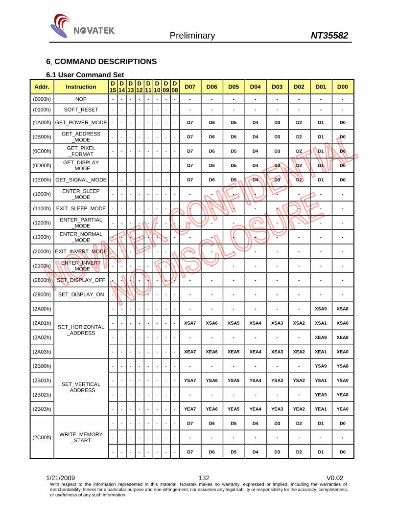
Preliminary NT35582
1/21/2009 132 V0.02 With respect to the information represented in this material, Novatek makes no warranty, expressed or implied, including the warranties of merchantability, fitness for a particular purpose and non-infringement, nor assumes any legal liability or responsibility for the accuracy, completeness, or usefulness of any such information.
6. COMMAND DESCRIPTIONS 6.1 User Command Set
Addr. Instruction D15
D14
D13
D12
D11
D10
D09
D08 D07 D06 D05 D04 D03 D02 D01 D00
(0000h) NOP - - - - - - - - - - - - - - - -
(0100h) SOFT_RESET - - - - - - - - - - - - - - - -
(0A00h) GET_POWER_MODE - - - - - - - - D7 D6 D5 D4 D3 D2 D1 D0
(0B00h) GET_ADDRESS _MODE - - - - - - - - D7 D6 D5 D4 D3 D2 D1 D0
(0C00h) GET_PIXEL _FORMAT - - - - - - - - D7 D6 D5 D4 D3 D2 D1 D0
(0D00h) GET_DISPLAY _MODE - - - - - - - - D7 D6 D5 D4 D3 D2 D1 D0
(0E00h) GET_SIGNAL_MODE - - - - - - - - D7 D6 D5 D4 D3 D2 D1 D0
(1000h) ENTER_SLEEP _MODE - - - - - - - - - - - - - - - -
(1100h) EXIT_SLEEP_MODE - - - - - - - - - - - - - - - -
(1200h) ENTER_PARTIAL _MODE - - - - - - - - - - - - - - - -
(1300h) ENTER_NORMAL _MODE - - - - - - - - - - - - - - - -
(2000h) EXIT_INVERT_MODE - - - - - - - - - - - - - - - -
(2100h) ENTER_INVERT _MODE - - - - - - - - - - - - - - - -
(2800h) SET_DISPLAY_OFF - - - - - - - - - - - - - - - -
(2900h) SET_DISPLAY_ON - - - - - - - - - - - - - - - -
(2A00h) - - - - - - - - - - - - - - XSA9 XSA8
(2A01h) - - - - - - - - XSA7 XSA6 XSA5 XSA4 XSA3 XSA2 XSA1 XSA0
(2A02h) - - - - - - - - - - - - - - XEA9 XEA8
(2A03h)
SET_HORIZONTAL _ADDRESS
- - - - - - - - XEA7 XEA6 XEA5 XEA4 XEA3 XEA2 XEA1 XEA0
(2B00h) - - - - - - - - - - - - - - YSA9 YSA8
(2B01h) - - - - - - - - YSA7 YSA6 YSA5 YSA4 YSA3 YSA2 YSA1 YSA0
(2B02h) - - - - - - - - - - - - - - YEA9 YEA8
(2B03h)
SET_VERTICAL _ADDRESS
- - - - - - - - YEA7 YEA6 YEA5 YEA4 YEA3 YEA2 YEA1 YEA0
- - - - - - - - D7 D6 D5 D4 D3 D2 D1 D0
- - - - - - - - : : : : : : : : (2C00h) WRITE_MEMORY _START
- - - - - - - - D7 D6 D5 D4 D3 D2 D1 D0

Preliminary NT35582
1/21/2009 133 V0.02 With respect to the information represented in this material, Novatek makes no warranty, expressed or implied, including the warranties of merchantability, fitness for a particular purpose and non-infringement, nor assumes any legal liability or responsibility for the accuracy, completeness, or usefulness of any such information.
Addr. Instruction D15
D14
D13
D12
D11
D10
D09
D08 D07 D06 D05 D04 D03 D02 D01 D00
(2D00h) - - - - - - - - - - - - - - XAD9 XAD8
(2D01h) - - - - - - - - XAD7 XAD6 XAD5 XAD4 XAD3 XAD2 XAD1 XAD0
(2D02h) - - - - - - - - - - - - - - YAD9 YAD8
(2D03h)
SET_RAM_ADDRESS
- - - - - - - - YAD7 YAD6 YAD5 YAD4 YAD3 YAD2 YAD1 YAD0
- - - - - - - - D7 D6 D5 D4 D3 D2 D1 D0
- - - - - - - - : : : : : : : : (2E00h) READ_MEMORY _START
- - - - - - - - D7 D6 D5 D4 D3 D2 D1 D0
(3000h) - - - - - - - - PSL15 PSL14 PSL13 PSL12 PSL11 PSL10 PSL9 PSL8
(3001h) - - - - - - - - PSL7 PSL6 PSL5 PSL4 PSL3 PSL2 PSL1 PSL0
(3002h) - - - - - - - - PEL15 PEL14 PEL13 PEL12 PEL11 PEL10 PEL9 PEL8
(3003h)
SET_PARTIAL_AREA
- - - - - - - - PEL7 PEL6 PEL5 PEL4 PEL3 PEL2 PEL1 PEL0
(3400h) SET_TEAR_OFF - - - - - - - - - - - - - - - -
(3500h) SET_TEAR_ON - - - - - - - - TEW3 TEW2 TEW1 TEW0 - - TEP -
(3600h) SET_ADDRESS _MODE - - - - - - - - MY MX MV - RGB - CRL CTB
(3601h) SET_ADDRESS _MODE1 - - - - - - - - - - - - - - - HBM
(3800h) EXIT_IDLE_MODE - - - - - - - - - - - - - - - -
(3900h) ENTER_IDLE_MODE - - - - - - - - - - - - - - - -
(3A00h) SET_PIXEL_FORMAT - - - - - - - - - VIPF2 VIPF1 VIPF0 - IFPF2 IFPF1 IFPF0
(3B00h) RGBCTRL - - - - - - - - - CRCM HDSM ICM DP EP HSP VSP
(3B02h) VBP - - - - - - - - - - VBP5 VBP4 VBP3 VBP2 VBP1 VBP0
(3B03h) VFP - - - - - - - - - - VFP5 VFP4 VFP3 VFP2 VFP1 VFP0
(3B04h) HBP - - - - - - - - - - HBP5 HBP4 HBP3 HBP2 HBP1 HBP0
(3B05h) HFP - - - - - - - - - - HFP5 HFP4 HFP3 HFP2 HFP1 HFP0
(4400h) - - - - - - - - - - - - - - N9 N8
(4401h)
SET_TEAR _SCANLINE
- - - - - - - - N7 N6 N5 N4 N3 N2 N1 N0
(4D00h) SET_IM3 - - - - - - - - - - - - - - - CIM3
(4E00h) SPI_I2C_SEL - - - - - - - - - - - - - - - SPI_I2C
(4F00h) ENTER_DSTB _MODE - - - - - - - - - - - - - - - DSTB
Addr. Instruction D15
D14
D13
D12
D11
D10
D09
D08 D07 D06 D05 D04 D03 D02 D01 D00

Preliminary NT35582
1/21/2009 134 V0.02 With respect to the information represented in this material, Novatek makes no warranty, expressed or implied, including the warranties of merchantability, fitness for a particular purpose and non-infringement, nor assumes any legal liability or responsibility for the accuracy, completeness, or usefulness of any such information.
(5000h) - - - - - - - - STEP_OUT_DP0
[7]
STEP_OUT_DP0
[6]
STEP_OUT_DP0
[5]
STEP_OUT_DP0
[4]
STEP_OUT_DP0
[3]
STEP_OUT_DP0
[2]
STEP_OUT_DP0
[1]
STEP_OUT_DP0
[0]
(5001h) - - - - - - - - STEP_OUT_DP1
[7]
STEP_OUT_DP1
[6]
STEP_OUT_DP1
[5]
STEP_OUT_DP1
[4]
STEP_OUT_DP1
[3]
STEP_OUT_DP1
[2]
STEP_OUT_DP1
[1]
STEP_OUT_DP1
[0]
(5002h) - - - - - - - - STEP_OUT_DP2
[7]
STEP_OUT_DP2
[6]
STEP_OUT_DP2
[5]
STEP_OUT_DP2
[4]
STEP_OUT_DP2
[3]
STEP_OUT_DP2
[2]
STEP_OUT_DP2
[1]
STEP_OUT_DP2
[0]
(5003h) - - - - - - - - STEP_OUT_DP3
[7]
STEP_OUT_DP3
[6]
STEP_OUT_DP3
[5]
STEP_OUT_DP3
[4]
STEP_OUT_DP3
[3]
STEP_OUT_DP3
[2]
STEP_OUT_DP3
[1]
STEP_OUT_DP3
[0]
(5004h) - - - - - - - - STEP_OUT_DP4
[7]
STEP_OUT_DP4
[6]
STEP_OUT_DP4
[5]
STEP_OUT_DP4
[4]
STEP_OUT_DP4
[3]
STEP_OUT_DP4
[2]
STEP_OUT_DP4
[1]
STEP_OUT_DP4
[0]
(5005h) - - - - - - - - STEP_OUT_DP5
[7]
STEP_OUT_DP5
[6]
STEP_OUT_DP5
[5]
STEP_OUT_DP5
[4]
STEP_OUT_DP5
[3]
STEP_OUT_DP5
[2]
STEP_OUT_DP5
[1]
STEP_OUT_DP5
[0]
(5006h) - - - - - - - - STEP_OUT_DP6
[7]
STEP_OUT_DP6
[6]
STEP_OUT_DP6
[5]
STEP_OUT_DP6
[4]
STEP_OUT_DP6
[3]
STEP_OUT_DP6
[2]
STEP_OUT_DP6
[1]
STEP_OUT_DP6
[0]
(5007h) - - - - - - - - STEP_OUT_DP7
[7]
STEP_OUT_DP7
[6]
STEP_OUT_DP7
[5]
STEP_OUT_DP7
[4]
STEP_OUT_DP7
[3]
STEP_OUT_DP7
[2]
STEP_OUT_DP7
[1]
STEP_OUT_DP7
[0]
(5008h) - - - - - - - - STEP_OUT_DP8
[7]
STEP_OUT_DP8
[6]
STEP_OUT_DP8
[5]
STEP_OUT_DP8
[4]
STEP_OUT_DP8
[3]
STEP_OUT_DP8
[2]
STEP_OUT_DP8
[1]
STEP_OUT_DP8
[0]
(5009h) - - - - - - - - STEP_OUT_DP9
[7]
STEP_OUT_DP9
[6]
STEP_OUT_DP9
[5]
STEP_OUT_DP9
[4]
STEP_OUT_DP9
[3]
STEP_OUT_DP9
[2]
STEP_OUT_DP9
[1]
STEP_OUT_DP9
[0]
(500Ah) - - - - - - - - STEP_OUT_DP1
0[7]
STEP_OUT_DP1
0[6]
STEP_OUT_DP1
0[5]
STEP_OUT_DP10
[4]
STEP_OUT_DP1
0[3]
STEP_OUT_DP1
0[2]
STEP_OUT_DP1
0[1]
STEP_OUT_DP1
0[0]
(500Bh) - - - - - - - - STEP_OUT_DP1
1[7]
STEP_OUT_DP1
1[6]
STEP_OUT_DP1
1[5]
STEP_OUT_DP11
[4]
STEP_OUT_DP1
1[3]
STEP_OUT_DP1
1[2]
STEP_OUT_DP1
1[1]
STEP_OUT_DP1
1[0]
(500Ch) - - - - - - - - STEP_OUT_DP1
2[7]
STEP_OUT_DP1
2[6]
STEP_OUT_DP1
2[5]
STEP_OUT_DP12
[4]
STEP_OUT_DP1
2[3]
STEP_OUT_DP1
2[2]
STEP_OUT_DP1
2[1]
STEP_OUT_DP1
2[0]
(500Dh) - - - - - - - - STEP_OUT_DP1
3[7]
STEP_OUT_DP1
3[6]
STEP_OUT_DP1
3[5]
STEP_OUT_DP13
[4]
STEP_OUT_DP1
3[3]
STEP_OUT_DP1
3[2]
STEP_OUT_DP1
3[1]
STEP_OUT_DP1
3[0]
(500Eh) - - - - - - - - STEP_OUT_DP1
4[7]
STEP_OUT_DP1
4[6]
STEP_OUT_DP1
4[5]
STEP_OUT_DP14
[4]
STEP_OUT_DP1
4[3]
STEP_OUT_DP1
4[2]
STEP_OUT_DP1
4[1]
STEP_OUT_DP1
4[0]
(500Fh)
WRPFD
- - - - - - - - STEP_OUT_DP1
5[7]
STEP_OUT_DP1
5[6]
STEP_OUT_DP1
5[5]
STEP_OUT_DP15
[4]
STEP_OUT_DP1
5[3]
STEP_OUT_DP1
5[2]
STEP_OUT_DP1
5[1]
STEP_OUT_DP1
5[0]
(5100h) WRDISBV - - - - - - - - DBV[7] DBV[6] DBV[5] DBV[4] DBV[3] DBV[2] DBV[1] DBV[0]
(5200h) RDDISBV - - - - - - - - DBV[7] DBV[6] DBV[5] DBV[4] DBV[3] DBV[2] DBV[1] DBV[0]
(5300h) WRCTRLD - - - - - - - - - - BCTRL A DD BL - -
(5301h) CTRLEDPWM - - - - - - - - - - - PWM_ENH_OE
CLED_VOL
LEDPWPOL
LEDONPOL LEDONR
(5302h) CTRDIM_L - - - - - - - - - - - - - - - DDL
(5303h) DIMPRDIN_L - - - - - - - - SEL_IN - - - DM_IN[3] DM_IN[2] DM_IN[1] DM_IN[0]

Preliminary NT35582
1/21/2009 135 V0.02 With respect to the information represented in this material, Novatek makes no warranty, expressed or implied, including the warranties of merchantability, fitness for a particular purpose and non-infringement, nor assumes any legal liability or responsibility for the accuracy, completeness, or usefulness of any such information.
Addr. Instruction D15
D14
D13
D12
D11
D10
D09
D08 D07 D06 D05 D04 D03 D02 D01 D00
(5304h) DIMPRDDE_L - - - - - - - - SEL_DE - - - DM_DE [3]
DM_DE [2]
DM_DE [1]
DM_DE [0]
(5305h) DMSTP_L - - - - - - - - - - - - - DMSTP_L[2]
DMSTP_L[1]
DMSTP_L[0]
(5306h) DMFIXSP_L - - - - - - - - STEP_DE[3]
STEP_DE[2]
STEP_DE[1]
STEP_DE[0]
STEP_IN[3]
STEP_IN[2]
STEP_IN[1]
STEP_IN[0]
(5307h) DMSPSTILL_C - - - - - - - - - - - - - DIM_STEP_STILL
[2]
DIM_STEP_STILL
[1]
DIM_STEP_STILL
[0]
(5308h) DMSPMOV_C - - - - - - - - - - - - - DIM_STEP_MOV
[2]
DIM_STEP_MOV
[1]
DIM_STEP_MOV
[0]
(5309h) DMST_C - - - - - - - - - - - - DMST_C[3]
DMST_C[2]
DMST_C[1]
DMST_C[0]
(5400h) RDCTRLD - - - - - - - - - - BCTRL A DD BL - -
(5401h) RDCTRLEDPWM - - - - - - - - - - - PWM_ENH_OE
CLED_VOL
LEDPWPOL
LEDONPOL LEDONR
(5402h) RDCTRDIML_L - - - - - - - - - - - - - - - DDL
(5403h) RDDIMPRDIN_L - - - - - - - - SEL_IN - - - DM_IN[3] DM_IN[2] DM_IN[1] DM_IN[0]
(5404h) RDDIMPRDDE_L - - - - - - - - SEL_DE - - - DM_DE [3]
DM_DE [2]
DM_DE [1]
DM_DE [0]
(5405h) RDDMSTP_L - - - - - - - - - - - - - DMSTP_L[2]
DMSTP_L[1]
DMSTP_L[0]
(5406h) RDDMFIXSP_L - - - - - - - - STEP_DE[3]
STEP_DE[2]
STEP_DE[1]
STEP_DE[0]
STEP_IN[3]
STEP_IN[2]
STEP_IN[1]
STEP_IN[0]
(5407h) RDDMSPSTILL_C - - - - - - - - - - - - - DIM_STEP_STILL
[2]
DIM_STEP_STILL
[1]
DIM_STEP_STILL
[0]
(5408h) RDDMSPMOV_C - - - - - - - - - - - - - DIM_STEP_MOV
[2]
DIM_STEP_MOV
[1]
DIM_STEP_MOV
[0]
(5409h) RDDMST_C - - - - - - - - - - - - DMST_C[3]
DMST_C[2]
DMST_C[1]
DMST_C[0]
(5500h) WRCABC - - - - - - - - - - - - - - CABC_COND[1]
CABC_COND[0]
(5600h) RDCABC - - - - - - - - - - - - - - CABC_COND[1]
CABC_COND[0]

Preliminary NT35582
1/21/2009 136 V0.02 With respect to the information represented in this material, Novatek makes no warranty, expressed or implied, including the warranties of merchantability, fitness for a particular purpose and non-infringement, nor assumes any legal liability or responsibility for the accuracy, completeness, or usefulness of any such information.
Addr. Instruction D15
D14
D13
D12
D11
D10
D09
D08 D07 D06 D05 D04 D03 D02 D01 D00
(5700h) - - - - - - - - I01[15] I01[14] I01[13] I01[12] I01[11] I01[10] I01[9] I01[8]
(5701h) - - - - - - - - I01[7] I01[6] I01[5] I01[4] I01[3] I01[2] I01[1] I01[0]
(5702h) - - - - - - - - D01[15] D01[14] D01[13] D01[12] D01[11] D01[10] D01[9] D01[8]
(5703h) - - - - - - - - D01[7] D01[6] D01[5] D01[4] D01[3] D01[2] D01[1] D01[0]
(5704h) - - - - - - - - I02[15] I02[14] I02[13] I02[12] I02[11] I02[10] I02[9] I02[8]
(5705h) - - - - - - - - I02[7] I02[6] I02[5] I02[4] I02[3] I02[2] I02[1] I02[0]
(5706h) - - - - - - - - D02[15] D02[14] D02[13] D02[12] D02[11] D02[10] D02[9] D02[8]
(5707h) - - - - - - - - D02[7] D02[6] D02[5] D02[4] D02[3] D02[2] D02[1] D02[0]
(5708h) - - - - - - - - I03[15] I03[14] I03[13] I03[12] I03[11] I03[10] I03[9] I03[8]
(5709h) - - - - - - - - I03[7] I03[6] I03[5] I03[4] I03[3] I03[2] I03[1] I03[0]
(570Ah) - - - - - - - - D03[15] D03[14] D03[13] D03[12] D03[11] D03[10] D03[9] D03[8]
(570Bh) - - - - - - - - D03[7] D03[6] D03[5] D03[4] D03[3] D03[2] D03[1] D03[0]
(570Ch) - - - - - - - - I04[15] I04[14] I04[13] I04[12] I04[11] I04[10] I04[9] I04[8]
(570Dh) - - - - - - - - I04[7] I04[6] I04[5] I04[4] I04[3] I04[2] I04[1] I04[0]
(570Eh) - - - - - - - - D04[15] D04[14] D04[13] D04[12] D04[11] D04[10] D04[9] D04[8]
(570Fh) - - - - - - - - D04[7] D04[6] D04[5] D04[4] D04[3] D04[2] D04[1] D04[0]
(5710h) - - - - - - - - I05[15] I05[14] I05[13] I05[12] I05[11] I05[10] I05[9] I05[8]
(5711h) - - - - - - - - I05[7] I05[6] I05[5] I05[4] I05[3] I05[2] I05[1] I05[0]
(5712h) - - - - - - - - D05[15] D05[14] D05[13] D05[12] D05[11] D05[10] D05[9] D05[8]
(5713h) - - - - - - - - D05[7] D05[6] D05[5] D05[4] D05[3] D05[2] D05[1] D05[0]
(5714h) - - - - - - - - I06[15] I06[14] I06[13] I06[12] I06[11] I06[10] I06[9] I06[8]
(5715h) - - - - - - - - I06[7] I06[6] I06[5] I06[4] I06[3] I06[2] I06[1] I06[0]
(5716h) - - - - - - - - D06[15] D06[14] D06[13] D06[12] D06[11] D06[10] D06[9] D06[8]
(5717h)
WRHYSTER
- - - - - - - - D06[7] D06[6] D06[5] D06[4] D06[3] D06[2] D06[1] D06[0]
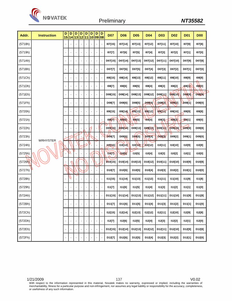
Preliminary NT35582
1/21/2009 137 V0.02 With respect to the information represented in this material, Novatek makes no warranty, expressed or implied, including the warranties of merchantability, fitness for a particular purpose and non-infringement, nor assumes any legal liability or responsibility for the accuracy, completeness, or usefulness of any such information.
Addr. Instruction D15
D14
D13
D12
D11
D10
D09
D08 D07 D06 D05 D04 D03 D02 D01 D00
(5718h) - - - - - - - - I07[15] I07[14] I07[13] I07[12] I07[11] I07[10] I07[9] I07[8]
(5719h) - - - - - - - - I07[7] I07[6] I07[5] I07[4] I07[3] I07[2] I07[1] I07[0]
(571Ah) - - - - - - - - D07[15] D07[14] D07[13] D07[12] D07[11] D07[10] D07[9] D07[8]
(571Bh) - - - - - - - - D07[7] D07[6] D07[5] D07[4] D07[3] D07[2] D07[1] D07[0]
(571Ch) - - - - - - - - I08[15] I08[14] I08[13] I08[12] I08[11] I08[10] I08[9] I08[8]
(571Dh) - - - - - - - - I08[7] I08[6] I08[5] I08[4] I08[3] I08[2] I08[1] I08[0]
(571Eh) - - - - - - - - D08[15] D08[14] D08[13] D08[12] D08[11] D08[10] D08[9] D08[8]
(571Fh) - - - - - - - - D08[7] D08[6] D08[5] D08[4] D08[3] D08[2] D08[1] D08[0]
(5720h) - - - - - - - - I09[15] I09[14] I09[13] I09[12] I09[11] I09[10] I09[9] I09[8]
(5721h) - - - - - - - - I09[7] I09[6] I09[5] I09[4] I09[3] I09[2] I09[1] I09[0]
(5722h) - - - - - - - - D09[15] D09[14] D09[13] D09[12] D09[11] D09[10] D09[9] D09[8]
(5723h) - - - - - - - - D09[7] D09[6] D09[5] D09[4] D09[3] D09[2] D09[1] D09[0]
(5724h) - - - - - - - - I10[15] I10[14] I10[13] I10[12] I10[11] I10[10] I10[9] I10[8]
(5725h) - - - - - - - - I10[7] I10[6] I10[5] I10[4] I10[3] I10[2] I10[1] I10[0]
(5726h) - - - - - - - - D10[15] D10[14] D10[13] D10[12] D10[11] D10[10] D10[9] D10[8]
(5727h) - - - - - - - - D10[7] D10[6] D10[5] D10[4] D10[3] D10[2] D10[1] D10[0]
(5728h) - - - - - - - - I11[15] I11[14] I11[13] I11[12] I11[11] I11[10] I11[9] I11[8]
(5729h) - - - - - - - - I11[7] I11[6] I11[5] I11[4] I11[3] I11[2] I11[1] I11[0]
(572Ah) - - - - - - - - D11[15] D11[14] D11[13] D11[12] D11[11] D11[10] D11[9] D11[8]
(572Bh) - - - - - - - - D11[7] D11[6] D11[5] D11[4] D11[3] D11[2] D11[1] D11[0]
(572Ch) - - - - - - - - I12[15] I12[14] I12[13] I12[12] I12[11] I12[10] I12[9] I12[8]
(572Dh) - - - - - - - - I12[7] I12[6] I12[5] I12[4] I12[3] I12[2] I12[1] I12[0]
(572Eh) - - - - - - - - D12[15] D12[14] D12[13] D12[12] D12[11] D12[10] D12[9] D12[8]
(572Fh)
WRHYSTER
- - - - - - - - D12[7] D12[6] D12[5] D12[4] D12[3] D12[2] D12[1] D12[0]
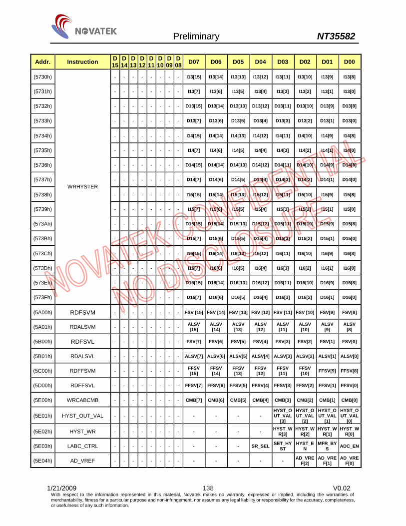
Preliminary NT35582
1/21/2009 138 V0.02 With respect to the information represented in this material, Novatek makes no warranty, expressed or implied, including the warranties of merchantability, fitness for a particular purpose and non-infringement, nor assumes any legal liability or responsibility for the accuracy, completeness, or usefulness of any such information.
Addr. Instruction D15
D14
D13
D12
D11
D10
D09
D08 D07 D06 D05 D04 D03 D02 D01 D00
(5730h) - - - - - - - - I13[15] I13[14] I13[13] I13[12] I13[11] I13[10] I13[9] I13[8]
(5731h) - - - - - - - - I13[7] I13[6] I13[5] I13[4] I13[3] I13[2] I13[1] I13[0]
(5732h) - - - - - - - - D13[15] D13[14] D13[13] D13[12] D13[11] D13[10] D13[9] D13[8]
(5733h) - - - - - - - - D13[7] D13[6] D13[5] D13[4] D13[3] D13[2] D13[1] D13[0]
(5734h) - - - - - - - - I14[15] I14[14] I14[13] I14[12] I14[11] I14[10] I14[9] I14[8]
(5735h) - - - - - - - - I14[7] I14[6] I14[5] I14[4] I14[3] I14[2] I14[1] I14[0]
(5736h) - - - - - - - - D14[15] D14[14] D14[13] D14[12] D14[11] D14[10] D14[9] D14[8]
(5737h) - - - - - - - - D14[7] D14[6] D14[5] D14[4] D14[3] D14[2] D14[1] D14[0]
(5738h) - - - - - - - - I15[15] I15[14] I15[13] I15[12] I15[11] I15[10] I15[9] I15[8]
(5739h) - - - - - - - - I15[7] I15[6] I15[5] I15[4] I15[3] I15[2] I15[1] I15[0]
(573Ah) - - - - - - - - D15[15] D15[14] D15[13] D15[12] D15[11] D15[10] D15[9] D15[8]
(573Bh) - - - - - - - - D15[7] D15[6] D15[5] D15[4] D15[3] D15[2] D15[1] D15[0]
(573Ch) - - - - - - - - I16[15] I16[14] I16[13] I16[12] I16[11] I16[10] I16[9] I16[8]
(573Dh) - - - - - - - - I16[7] I16[6] I16[5] I16[4] I16[3] I16[2] I16[1] I16[0]
(573Eh) - - - - - - - - D16[15] D16[14] D16[13] D16[12] D16[11] D16[10] D16[9] D16[8]
(573Fh)
WRHYSTER
- - - - - - - - D16[7] D16[6] D16[5] D16[4] D16[3] D16[2] D16[1] D16[0]
(5A00h) RDFSVM - - - - - - - - FSV [15] FSV [14] FSV [13] FSV [12] FSV [11] FSV [10] FSV[9] FSV[8]
(5A01h) RDALSVM - - - - - - - - ALSV [15]
ALSV [14]
ALSV [13]
ALSV [12]
ALSV [11]
ALSV [10]
ALSV [9]
ALSV [8]
(5B00h) RDFSVL - - - - - - - - FSV[7] FSV[6] FSV[5] FSV[4] FSV[3] FSV[2] FSV[1] FSV[0]
(5B01h) RDALSVL - - - - - - - - ALSV[7] ALSV[6] ALSV[5] ALSV[4] ALSV[3] ALSV[2] ALSV[1] ALSV[0]
(5C00h) RDFFSVM - - - - - - - - FFSV [15]
FFSV [14]
FFSV [13]
FFSV [12]
FFSV [11]
FFSV [10] FFSV[9] FFSV[8]
(5D00h) RDFFSVL - - - - - - - - FFSV[7] FFSV[6] FFSV[5] FFSV[4] FFSV[3] FFSV[2] FFSV[1] FFSV[0]
(5E00h) WRCABCMB - - - - - - - - CMB[7] CMB[6] CMB[5] CMB[4] CMB[3] CMB[2] CMB[1] CMB[0]
(5E01h) HYST_OUT_VAL - - - - - - - - - - - - HYST_OUT_VAL
[3]
HYST_OUT_VAL
[2]
HYST_OUT_VAL
[1]
HYST_OUT_VAL
[0]
(5E02h) HYST_WR - - - - - - - - - - - - HYST_WR[3]
HYST_WR[2]
HYST_WR[1]
HYST_WR[0]
(5E03h) LABC_CTRL - - - - - - - - - - - SR_SEL SET_HYST
HYST_EN
MFR_BYS ADC_EN
(5E04h) AD_VREF - - - - - - - - - - - - - AD_VREF[2]
AD_VREF[1]
AD_VREF[0]
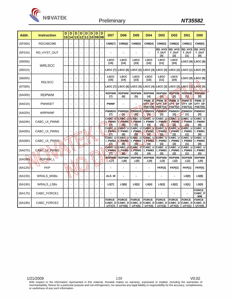
Preliminary NT35582
1/21/2009 139 V0.02 With respect to the information represented in this material, Novatek makes no warranty, expressed or implied, including the warranties of merchantability, fitness for a particular purpose and non-infringement, nor assumes any legal liability or responsibility for the accuracy, completeness, or usefulness of any such information.
Addr. Instruction D15
D14
D13
D12
D11
D10
D09
D08 D07 D06 D05 D04 D03 D02 D01 D00
(5F00h) RDCABCMB - - - - - - - - CMB[7] CMB[6] CMB[5] CMB[4] CMB[3] CMB[2] CMB[1] CMB[0]
(5F01h) RD_HYST_OUT - - - - - - - - - - - - RD_HYST_OUT
[3]
RD_HYST_OUT
[2]
RD_HYST_OUT
[1]
RD_HYST_OUT
[0]
(6500h) - - - - - - - - LSCC [15]
LSCC [14]
LSCC [13]
LSCC [12]
LSCC [11]
LSCC [10] LSCC [9] LSCC [8]
(6501h) WRLSCC
- - - - - - - - LSCC [7] LSCC [6] LSCC [5] LSCC [4] LSCC [3] LSCC [2] LSCC [1] LSCC [0]
(6600h) - - - - - - - - LSCC [15]
LSCC [14]
LSCC [13]
LSCC [12]
LSCC [11]
LSCC [10] LSCC [9] LSCC [8]
(6700h) RDLSCC
- - - - - - - - LSCC [7] LSCC [6] LSCC [5] LSCC [4] LSCC [3] LSCC [2] LSCC [1] LSCC [0]
(6A00h) RDPWM - - - - - - - - RDPWM [7]
RDPWM [6]
RDPWM [5]
RDPWM [4]
RDPWM [3]
RDPWM [2]
RDPWM [1]
RDPWM [0]
(6A01h) PWMSET - - - - - - - - PWMF - - PWM_DUTY_OFFSET[4]
PWM_DUTY_OFFSET[3]
PWM_DUTY_OFFSET[2]
PWM_DUTY_OFFSET[1]
PWM_DUTY_OFFSET[0]
(6A02h) WRPWMF - - - - - - - - PWMDIV[7]
PWMDIV[6]
PWMDIV[5]
PWMDIV[4]
PWMDIV[3]
PWMDIV[2]
PWMDIV[1]
PWMDIV[0]
(6A04h) CABC_UI_PWM0 - - - - - - - - CABC_UI_PWM0
[7]
CABC_UI_PWM0
[6]
CABC_UI_PWM0
[5]
CABC_UI_PWM0
[4]
CABC_UI_PWM0
[3]
CABC_UI_PWM0
[2]
CABC_UI_PWM0
[1]
CABC_UI_PWM0
[0]
(6A05h) CABC_UI_PWM1 - - - - - - - - CABC_UI_PWM1
[7]
CABC_UI_PWM1
[6]
CABC_UI_PWM1
[5]
CABC_UI_PWM1
[4]
CABC_UI_PWM1
[3]
CABC_UI_PWM1
[2]
CABC_UI_PWM1
[1]
CABC_UI_PWM1
[0]
(6A06h) CABC_UI_PWM2 - - - - - - - - CABC_UI_PWM2
[7]
CABC_UI_PWM2
[6]
CABC_UI_PWM2
[5]
CABC_UI_PWM2
[4]
CABC_UI_PWM2
[3]
CABC_UI_PWM2
[2]
CABC_UI_PWM2
[1]
CABC_UI_PWM2
[0]
(6A07h) CABC_UI_PWM3 - - - - - - - - CABC_UI_PWM3
[7]
CABC_UI_PWM3
[6]
CABC_UI_PWM3
[5]
CABC_UI_PWM3
[4]
CABC_UI_PWM3
[3]
CABC_UI_PWM3
[2]
CABC_UI_PWM3
[1]
CABC_UI_PWM3
[0]
(6A09h) RDPWM_L - - - - - - - - RDPWM_L[7]
RDPWM_L[6]
RDPWM_L[5]
RDPWM_L[4]
RDPWM_L[3]
RDPWM_L[2]
RDPWM_L[1]
RDPWM_L[0]
(6A12h) FKP - - - - - - - - - - - - FKP[3] FKP[2] FKP[1] FKP[0]
(6A15h) WRALS_MSBs - - - - - - - - ALS_W - - - - - LS[9] LS[8]
(6A16h) WRALS_LSBs - - - - - - - - LS[7] LS[6] LS[5] LS[4] LS[3] LS[2] LS[1] LS[0]
(6A17h) CABC_FORCE1 - - - - - - - - - - - - - - - FORCE_CABC_P
WM
(6A18h) CABC_FORCE2 - - - - - - - - FORCE_CABC_DUTY[7]
FORCE_CABC_DUTY[6]
FORCE_CABC_DUTY[5]
FORCE_CABC_DUTY[4]
FORCE_CABC_DUTY[3]
FORCE_CABC_DUTY[2]
FORCE_CABC_DUTY[1]
FORCE_CABC_DUTY[0]

Preliminary NT35582
1/21/2009 140 V0.02 With respect to the information represented in this material, Novatek makes no warranty, expressed or implied, including the warranties of merchantability, fitness for a particular purpose and non-infringement, nor assumes any legal liability or responsibility for the accuracy, completeness, or usefulness of any such information.
Addr. Instruction D15
D14
D13
D12
D11
D10
D09
D08 D07 D06 D05 D04 D03 D02 D01 D00
(6B00h) CABC_PWM0 - - - - - - - - CABC_PWM0[7]
CABC_PWM0[6]
CABC_PWM0[5]
CABC_PWM0[4]
CABC_PWM0[3]
CABC_PWM0[2]
CABC_PWM0[1]
CABC_PWM0[0]
(6B01h) CABC_PWM1 - - - - - - - - CABC_PWM1[7]
CABC_PWM1[6]
CABC_PWM1[5]
CABC_PWM1[4]
CABC_PWM1[3]
CABC_PWM1[2]
CABC_PWM1[1]
CABC_PWM1[0]
(6B02h) CABC_PWM2 - - - - - - - - CABC_PWM2[7]
CABC_PWM2[6]
CABC_PWM2[5]
CABC_PWM2[4]
CABC_PWM2[3]
CABC_PWM2[2]
CABC_PWM2[1]
CABC_PWM2[0]
(6B03h) CABC_PWM3 - - - - - - - - CABC_PWM3[7]
CABC_PWM3[6]
CABC_PWM3[5]
CABC_PWM3[4]
CABC_PWM3[3]
CABC_PWM3[2]
CABC_PWM3[1]
CABC_PWM3[0]
(6B04h) CABC_PWM4 - - - - - - - - CABC_PWM4[7]
CABC_PWM4[6]
CABC_PWM4[5]
CABC_PWM4[4]
CABC_PWM4[3]
CABC_PWM4[2]
CABC_PWM4[1]
CABC_PWM4[0]
(6B05h) CABC_PWM5 - - - - - - - - CABC_PWM5[7]
CABC_PWM5[6]
CABC_PWM5[5]
CABC_PWM5[4]
CABC_PWM5[3]
CABC_PWM5[2]
CABC_PWM5[1]
CABC_PWM5[0]
(6B06h) CABC_PWM6 - - - - - - - - CABC_PWM6[7]
CABC_PWM6[6]
CABC_PWM6[5]
CABC_PWM6[4]
CABC_PWM6[3]
CABC_PWM6[2]
CABC_PWM6[1]
CABC_PWM6[0]
(6B07h) CABC_PWM7 - - - - - - - - CABC_PWM7[7]
CABC_PWM7[6]
CABC_PWM7[5]
CABC_PWM7[4]
CABC_PWM7[3]
CABC_PWM7[2]
CABC_PWM7[1]
CABC_PWM7[0]
(6B08h) CABC_PWM8 - - - - - - - - CABC_PWM8[7]
CABC_PWM8[6]
CABC_PWM8[5]
CABC_PWM8[4]
CABC_PWM8[3]
CABC_PWM8[2]
CABC_PWM8[1]
CABC_PWM8[0]
(6B09h) CABC_PWM9 - - - - - - - - CABC_PWM9[7]
CABC_PWM9[6]
CABC_PWM9[5]
CABC_PWM9[4]
CABC_PWM9[3]
CABC_PWM9[2]
CABC_PWM9[1]
CABC_PWM9[0]
(6C0Dh) MOVDET - - - - - - - - - MOVDET[6]
MOVDET[5]
MOVDET[4]
MOVDET[3]
MOVDET[2]
MOVDET[1]
MOVDET[0]
(6C0Eh) MOVSC - - - - - - - - - - - MOVSC [4]
MOVSC [3]
MOVSC [2]
MOVSC [1]
MOVSC [0]
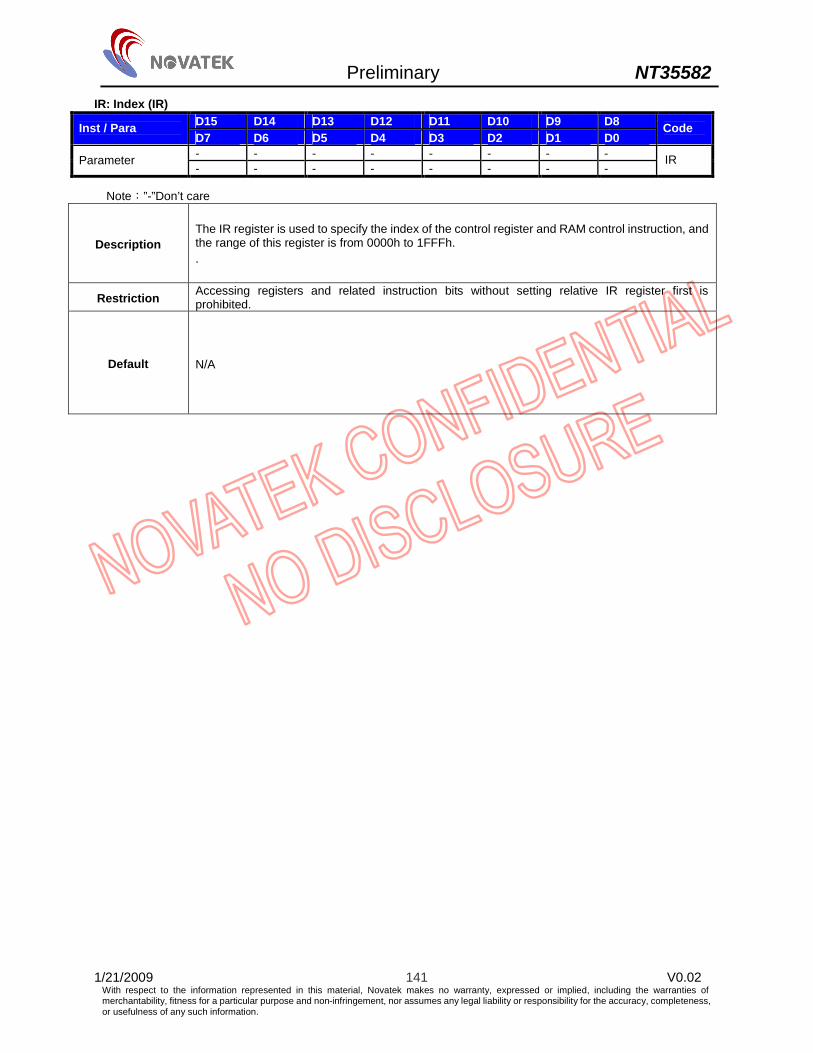
Preliminary NT35582
1/21/2009 141 V0.02 With respect to the information represented in this material, Novatek makes no warranty, expressed or implied, including the warranties of merchantability, fitness for a particular purpose and non-infringement, nor assumes any legal liability or responsibility for the accuracy, completeness, or usefulness of any such information.
IR: Index (IR) D15 D14 D13 D12 D11 D10 D9 D8 Inst / Para D7 D6 D5 D4 D3 D2 D1 D0
Code
- - - - - - - - Parameter - - - - - - - -
IR
Note:”-”Don’t care
Description The IR register is used to specify the index of the control register and RAM control instruction, and the range of this register is from 0000h to 1FFFh. .
Restriction Accessing registers and related instruction bits without setting relative IR register first is prohibited.
Default N/A

Preliminary NT35582
1/21/2009 142 V0.02 With respect to the information represented in this material, Novatek makes no warranty, expressed or implied, including the warranties of merchantability, fitness for a particular purpose and non-infringement, nor assumes any legal liability or responsibility for the accuracy, completeness, or usefulness of any such information.
NOP: No Operation (0000h) D15 D14 D13 D12 D11 D10 D9 D8 Inst / Para D7 D6 D5 D4 D3 D2 D1 D0
Code
- - - - - - - - Parameter - - - - - - - -
0000h
Note:”-”Don’t care
Description This command performs no operation and is ignored by the device.
Restriction -
Default N/A

Preliminary NT35582
1/21/2009 143 V0.02 With respect to the information represented in this material, Novatek makes no warranty, expressed or implied, including the warranties of merchantability, fitness for a particular purpose and non-infringement, nor assumes any legal liability or responsibility for the accuracy, completeness, or usefulness of any such information.
SOFT_RESET: Software Reset (0100h) D15 D14 D13 D12 D11 D10 D9 D8 Inst / Para D7 D6 D5 D4 D3 D2 D1 D0
Code
- - - - - - - - Parameter - - - - - - - -
0100h
Note:”-”Don’t care
Description -When the Software Reset command is set, it causes a software reset. It resets the commands and parameters to their S/W Reset register values and all source & gate outputs are set to GND (display off).
Restriction
-It will be necessary to wait 20msec before sending new command following software reset. The display module loads all display supplier’s factory default values to the registers during 20msec. -If Software Reset is applied during Sleep Out mode, it will be necessary to wait 120msec before sending Sleep Out command. -Software Reset command cannot be sent during Sleep Out sequence.
Default N/A

Preliminary NT35582
1/21/2009 144 V0.02 With respect to the information represented in this material, Novatek makes no warranty, expressed or implied, including the warranties of merchantability, fitness for a particular purpose and non-infringement, nor assumes any legal liability or responsibility for the accuracy, completeness, or usefulness of any such information.
GET_POWER_MODE: Read Display Power Mode (0A00h) D15 D14 D13 D12 D11 D10 D9 D8 Inst / Para D7 D6 D5 D4 D3 D2 D1 D0
Code
0 0 0 0 0 0 0 0 Parameter D7 D6 D5 D4 D3 D2 D1 D0
0A00h
Note:”-”Don’t care
Description
This command indicates the current status of the display as described in the table below: Bit Description Value D7 Booster Voltage Status “1” = Booster on, “0” = Booster off D6 Idle Mode On/Off “1” = Idle Mode On, “0” = Idle Mode Off D5 Partial Mode On/Off “1” = Partial Mode On, “0” = Partial Mode Off D4 Sleep In/Out “1” = Sleep Out, “0” = Sleep In
D3 Display Normal Mode On/Off “1” = Normal Display, “0” = Partial Display
D2 Display On/Off “1” = Display On, “0” = Display Off D1 Not Used “0” D0 Not Used “0”
Restriction -
Default
D15 D14 D13 D12 D11 D10 D09 D08 0 0 0 0 0 0 0 0
D07 D06 D05 D04 D03 D02 D01 D00 0 0 0 0 1 0 0 0

Preliminary NT35582
1/21/2009 145 V0.02 With respect to the information represented in this material, Novatek makes no warranty, expressed or implied, including the warranties of merchantability, fitness for a particular purpose and non-infringement, nor assumes any legal liability or responsibility for the accuracy, completeness, or usefulness of any such information.
GET_ADDRESS_MODE: Get the frame memory to the display panel read order (0B00h) D15 D14 D13 D12 D11 D10 D9 D8 Inst / Para D7 D6 D5 D4 D3 D2 D1 D0
Code
0 0 0 0 0 0 0 0 Parameter D7 D6 D5 D4 D3 D2 D1 D0
0B00h
Note:”-”Don’t care
Description
This command indicates the current status of the display as described in the table below: Bit Description Value D7 Row Address Order “1”=Decrement, “0”=Increment D6 Column Address Order “1”=Decrement, “0”=Increment
D5 Row/Column Order (MV) “1”= Row/column exchange (MV=1) “0”= Normal (MV=0)
D4 Vertical fresh Order & Display change (CTB) “1”=Decrement, “0”=Increment
D3 RGB/BGR Order “1”=BGR, “0”=RGB
D2 Horizontal fresh Order & Display change (CRL) “1”=Decrement, “0”=Increment
D1 Not Used “0” D0 Not Used “0”
Restriction -
Default
D15 D14 D13 D12 D11 D10 D09 D08 0 0 0 0 0 0 0 0
D07 D06 D05 D04 D03 D02 D01 D00 0 0 0 0 0 0 0 0
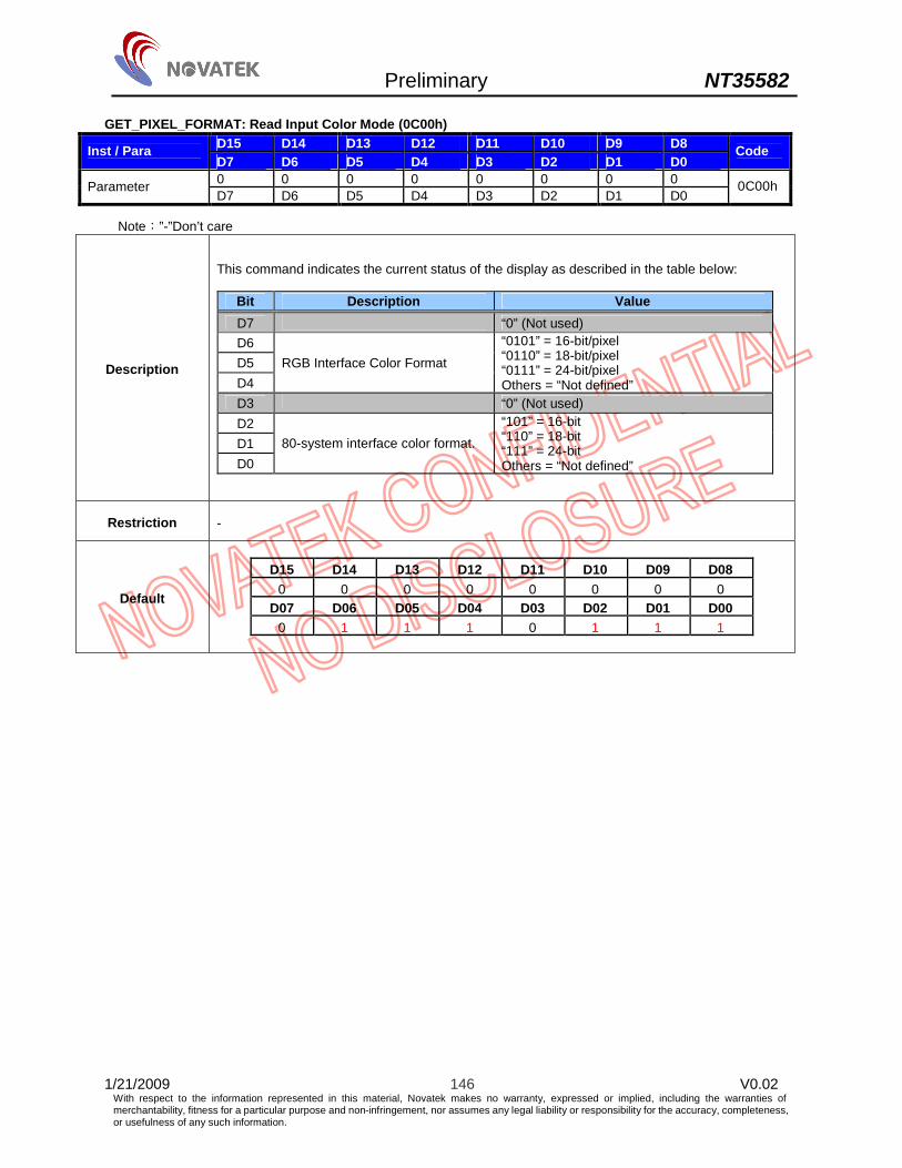
Preliminary NT35582
1/21/2009 146 V0.02 With respect to the information represented in this material, Novatek makes no warranty, expressed or implied, including the warranties of merchantability, fitness for a particular purpose and non-infringement, nor assumes any legal liability or responsibility for the accuracy, completeness, or usefulness of any such information.
GET_PIXEL_FORMAT: Read Input Color Mode (0C00h) D15 D14 D13 D12 D11 D10 D9 D8 Inst / Para D7 D6 D5 D4 D3 D2 D1 D0
Code
0 0 0 0 0 0 0 0 Parameter D7 D6 D5 D4 D3 D2 D1 D0
0C00h
Note:”-”Don’t care
Description
This command indicates the current status of the display as described in the table below:
Bit Description Value D7 “0” (Not used) D6 D5 D4
RGB Interface Color Format
“0101” = 16-bit/pixel “0110” = 18-bit/pixel “0111” = 24-bit/pixel Others = “Not defined”
D3 “0” (Not used) D2 D1 D0
80-system interface color format. “101” = 16-bit “110” = 18-bit “111” = 24-bit Others = “Not defined”
Restriction -
Default
D15 D14 D13 D12 D11 D10 D09 D08 0 0 0 0 0 0 0 0
D07 D06 D05 D04 D03 D02 D01 D00 0 1 1 1 0 1 1 1
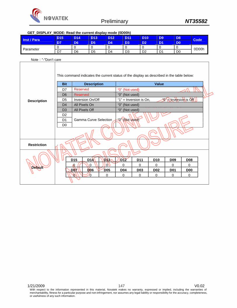
Preliminary NT35582
1/21/2009 147 V0.02 With respect to the information represented in this material, Novatek makes no warranty, expressed or implied, including the warranties of merchantability, fitness for a particular purpose and non-infringement, nor assumes any legal liability or responsibility for the accuracy, completeness, or usefulness of any such information.
GET_DISPLAY_MODE: Read the current display mode (0D00h) D15 D14 D13 D12 D11 D10 D9 D8 Inst / Para D7 D6 D5 D4 D3 D2 D1 D0
Code
0 0 0 0 0 0 0 0 Parameter D7 D6 D5 D4 D3 D2 D1 D0
0D00h
Note:”-”Don’t care
Description
This command indicates the current status of the display as described in the table below:
Bit Description Value D7 Reserved “0” (Not used) D6 Reserved “0” (Not used) D5 Inversion On/Off “1” = Inversion is On, “0” = Inversion is Off D4 All Pixels On “0” (Not used) D3 All Pixels Off “0” (Not used) D2 D1 D0
Gamma Curve Selection “0” (Not used)
Restriction -
Default
D15 D14 D13 D12 D11 D10 D09 D08 0 0 0 0 0 0 0 0
D07 D06 D05 D04 D03 D02 D01 D00 0 0 0 0 0 0 0 0

Preliminary NT35582
1/21/2009 148 V0.02 With respect to the information represented in this material, Novatek makes no warranty, expressed or implied, including the warranties of merchantability, fitness for a particular purpose and non-infringement, nor assumes any legal liability or responsibility for the accuracy, completeness, or usefulness of any such information.
GET_SIGNAL_MODE: Get display module signaling mode (0E00h) D15 D14 D13 D12 D11 D10 D9 D8 Inst / Para D7 D6 D5 D4 D3 D2 D1 D0
Code
0 0 0 0 0 0 0 0 Parameter D7 D6 D5 D4 D3 D2 D1 D0
0E00h
Note:”-”Don’t care
Description
This command indicates the current status of the display as described in the table below: Bit Description Value D7 Frame Tearing Effect Line On/Off “1” = On, “0” = Off D6 Reserved “0” (Not used) D5 Horizontal Sync. (RGB I/F) On/Off “1” = On, “0” = Off D4 Vertical Sync. (RGB I/F) On/Off “1” = On, “0” = Off D3 Pixel Clock (DCK, RGB I/F) On/Off “1” = On, “0” = Off D2 Data Enable (ENABLE, RGB I/F) On/Off “1” = On, “0” = Off D1 Not Used “0” (Not used) D0 Not Used “0” (Not used)
Restriction -
Default
D15 D14 D13 D12 D11 D10 D09 D08 0 0 0 0 0 0 0 0
D07 D06 D05 D04 D03 D02 D01 D00 0 0 0 0 0 0 0 0
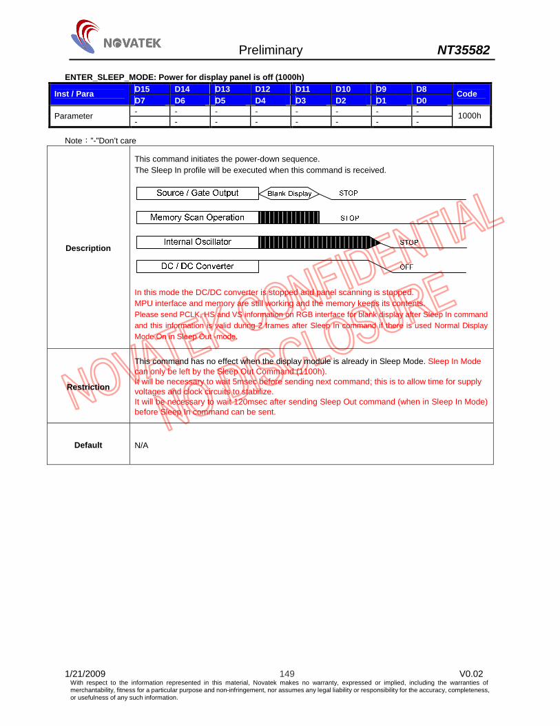
Preliminary NT35582
1/21/2009 149 V0.02 With respect to the information represented in this material, Novatek makes no warranty, expressed or implied, including the warranties of merchantability, fitness for a particular purpose and non-infringement, nor assumes any legal liability or responsibility for the accuracy, completeness, or usefulness of any such information.
ENTER_SLEEP_MODE: Power for display panel is off (1000h) D15 D14 D13 D12 D11 D10 D9 D8 Inst / Para D7 D6 D5 D4 D3 D2 D1 D0
Code
- - - - - - - - Parameter - - - - - - - -
1000h
Note:”-”Don’t care
Description
This command initiates the power-down sequence. The Sleep In profile will be executed when this command is received.
In this mode the DC/DC converter is stopped and panel scanning is stopped. MPU interface and memory are still working and the memory keeps its contents. Please send PCLK, HS and VS information on RGB interface for blank display after Sleep In command and this information is valid during 2 frames after Sleep In command if there is used Normal Display Mode On in Sleep Out -mode.
Restriction
This command has no effect when the display module is already in Sleep Mode. Sleep In Mode can only be left by the Sleep Out Command (1100h). It will be necessary to wait 5msec before sending next command; this is to allow time for supply voltages and clock circuits to stabilize. It will be necessary to wait 120msec after sending Sleep Out command (when in Sleep In Mode) before Sleep In command can be sent.
Default N/A

Preliminary NT35582
1/21/2009 150 V0.02 With respect to the information represented in this material, Novatek makes no warranty, expressed or implied, including the warranties of merchantability, fitness for a particular purpose and non-infringement, nor assumes any legal liability or responsibility for the accuracy, completeness, or usefulness of any such information.
EXIT_SLEEP_MODE: Power on for display panel (1100h) D15 D14 D13 D12 D11 D10 D9 D8 Inst / Para D7 D6 D5 D4 D3 D2 D1 D0
Code
- - - - - - - - Parameter - - - - - - - -
1100h
Note:”-”Don’t care
Description
This command initiates the power-up sequence. The Sleep Out profile will be executed when this command is received. The Sleep Out will load register value.
Please start to send PCLK, HS and VS information on RGB interface before Sleep Out command and this information is valid at least 2 frames before Sleep Out command, if there is left Sleep In mode to Sleep Out mode in Normal Display Mode On. There is used an internal oscillator for blank display.
Restriction
This command will not cause any visible effect on the display when the display is not in Sleep Mode. Sleep Out Mode can only be exit by the Sleep In Command (1000h). It will be necessary to wait 5msec before sending next command; this is to allow time for the supply voltages and clock circuits to stabilize. It will be necessary to wait 120msec after sending Sleep In command (when in Sleep Out mode) before Sleep Out command can be sent.
Default N/A
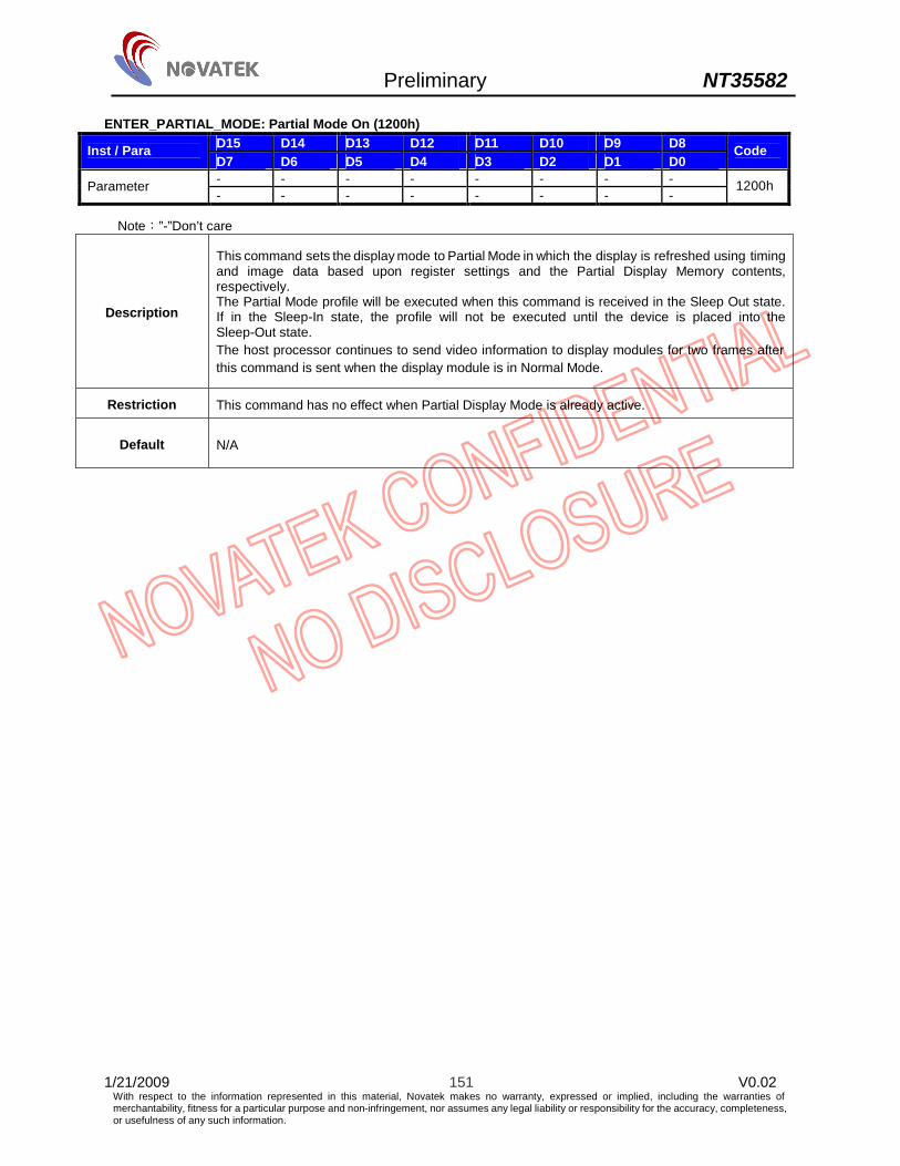
Preliminary NT35582
1/21/2009 151 V0.02 With respect to the information represented in this material, Novatek makes no warranty, expressed or implied, including the warranties of merchantability, fitness for a particular purpose and non-infringement, nor assumes any legal liability or responsibility for the accuracy, completeness, or usefulness of any such information.
ENTER_PARTIAL_MODE: Partial Mode On (1200h) D15 D14 D13 D12 D11 D10 D9 D8 Inst / Para D7 D6 D5 D4 D3 D2 D1 D0
Code
- - - - - - - - Parameter - - - - - - - -
1200h
Note:”-”Don’t care
Description
This command sets the display mode to Partial Mode in which the display is refreshed using timing and image data based upon register settings and the Partial Display Memory contents, respectively. The Partial Mode profile will be executed when this command is received in the Sleep Out state. If in the Sleep-In state, the profile will not be executed until the device is placed into the Sleep-Out state. The host processor continues to send video information to display modules for two frames after this command is sent when the display module is in Normal Mode.
Restriction This command has no effect when Partial Display Mode is already active.
Default N/A
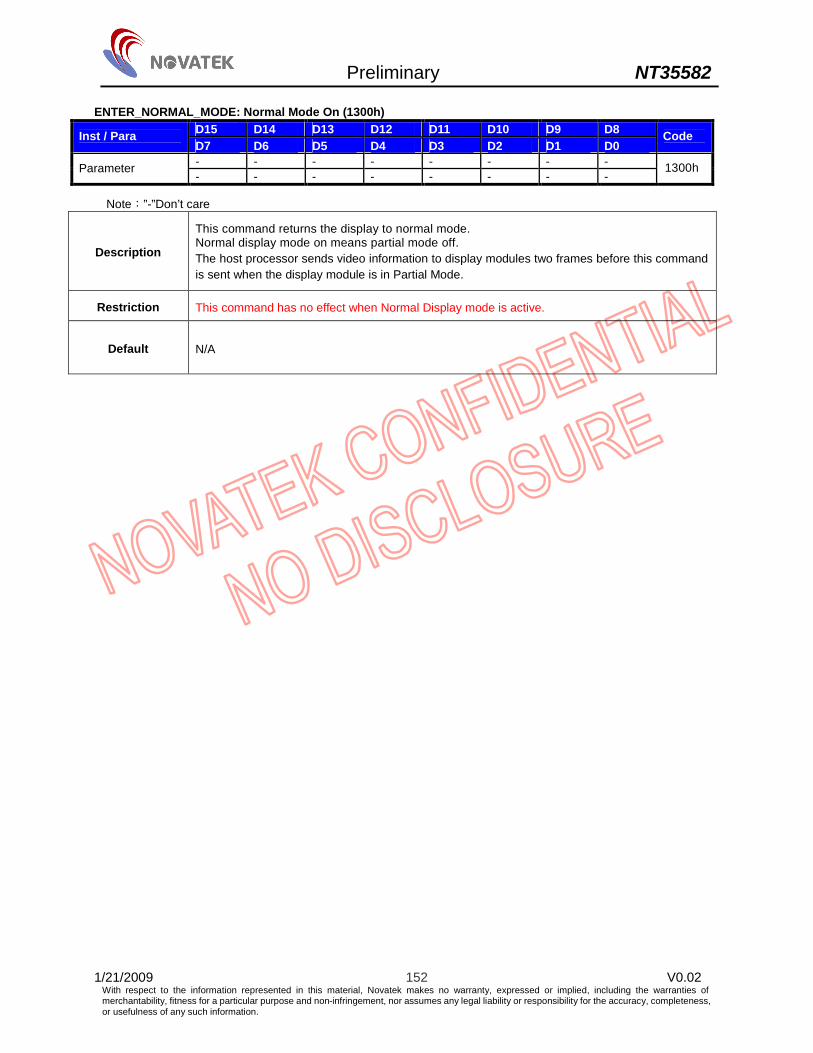
Preliminary NT35582
1/21/2009 152 V0.02 With respect to the information represented in this material, Novatek makes no warranty, expressed or implied, including the warranties of merchantability, fitness for a particular purpose and non-infringement, nor assumes any legal liability or responsibility for the accuracy, completeness, or usefulness of any such information.
ENTER_NORMAL_MODE: Normal Mode On (1300h) D15 D14 D13 D12 D11 D10 D9 D8 Inst / Para D7 D6 D5 D4 D3 D2 D1 D0
Code
- - - - - - - - Parameter - - - - - - - -
1300h
Note:”-”Don’t care
Description
This command returns the display to normal mode. Normal display mode on means partial mode off. The host processor sends video information to display modules two frames before this command is sent when the display module is in Partial Mode.
Restriction This command has no effect when Normal Display mode is active.
Default N/A

Preliminary NT35582
1/21/2009 153 V0.02 With respect to the information represented in this material, Novatek makes no warranty, expressed or implied, including the warranties of merchantability, fitness for a particular purpose and non-infringement, nor assumes any legal liability or responsibility for the accuracy, completeness, or usefulness of any such information.
EXIT_INVERT_MODE: Display colors are not inverted (2000h) D15 D14 D13 D12 D11 D10 D9 D8 Inst / Para D7 D6 D5 D4 D3 D2 D1 D0
Code
- - - - - - - - Parameter - - - - - - - -
2000h
Note:”-”Don’t care
Description
This command is used to recover from display inversion mode. This command makes no change of contents of frame memory. This command does not change any other status. (Example)
Memory Display
Restriction This command has no effect when the display is not inverting the display image.
Default N/A
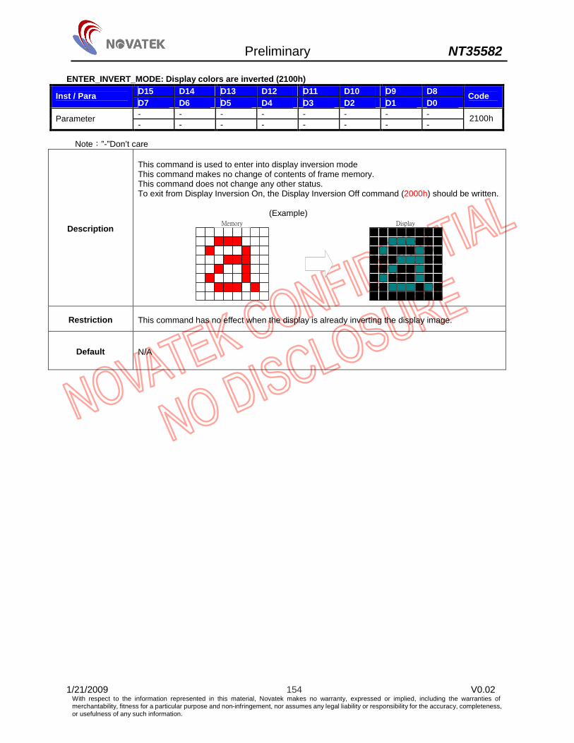
Preliminary NT35582
1/21/2009 154 V0.02 With respect to the information represented in this material, Novatek makes no warranty, expressed or implied, including the warranties of merchantability, fitness for a particular purpose and non-infringement, nor assumes any legal liability or responsibility for the accuracy, completeness, or usefulness of any such information.
ENTER_INVERT_MODE: Display colors are inverted (2100h) D15 D14 D13 D12 D11 D10 D9 D8 Inst / Para D7 D6 D5 D4 D3 D2 D1 D0
Code
- - - - - - - - Parameter - - - - - - - -
2100h
Note:”-”Don’t care
Description
This command is used to enter into display inversion mode This command makes no change of contents of frame memory. This command does not change any other status. To exit from Display Inversion On, the Display Inversion Off command (2000h) should be written. (Example)
Memory Display
Restriction This command has no effect when the display is already inverting the display image.
Default N/A

Preliminary NT35582
1/21/2009 155 V0.02 With respect to the information represented in this material, Novatek makes no warranty, expressed or implied, including the warranties of merchantability, fitness for a particular purpose and non-infringement, nor assumes any legal liability or responsibility for the accuracy, completeness, or usefulness of any such information.
SET_DISPALY_OFF: Blanking the display device (2800h) D15 D14 D13 D12 D11 D10 D9 D8 Inst / Para D7 D6 D5 D4 D3 D2 D1 D0
Code
- - - - - - - - Parameter - - - - - - - -
2800h
Note:”-”Don’t care
Description
This command will blank the display (white for normally white display and black for normally black display) regardless of the data on the video interface when in Normal Mode and regardless of the Partial Display Memory contents when in Partial Mode. This command does not affect the contents of the Partial Display Memory. The Display Off profile will be executed when this command is received in the Sleep Out state. If in the Sleep-In state, the profile will not be executed until the device is placed into the Sleep-Out state. Exit from this command by Display On (2900h)
(Example) Memory Display
Restriction This command has no effect when the display panel is already off.
Default N/A
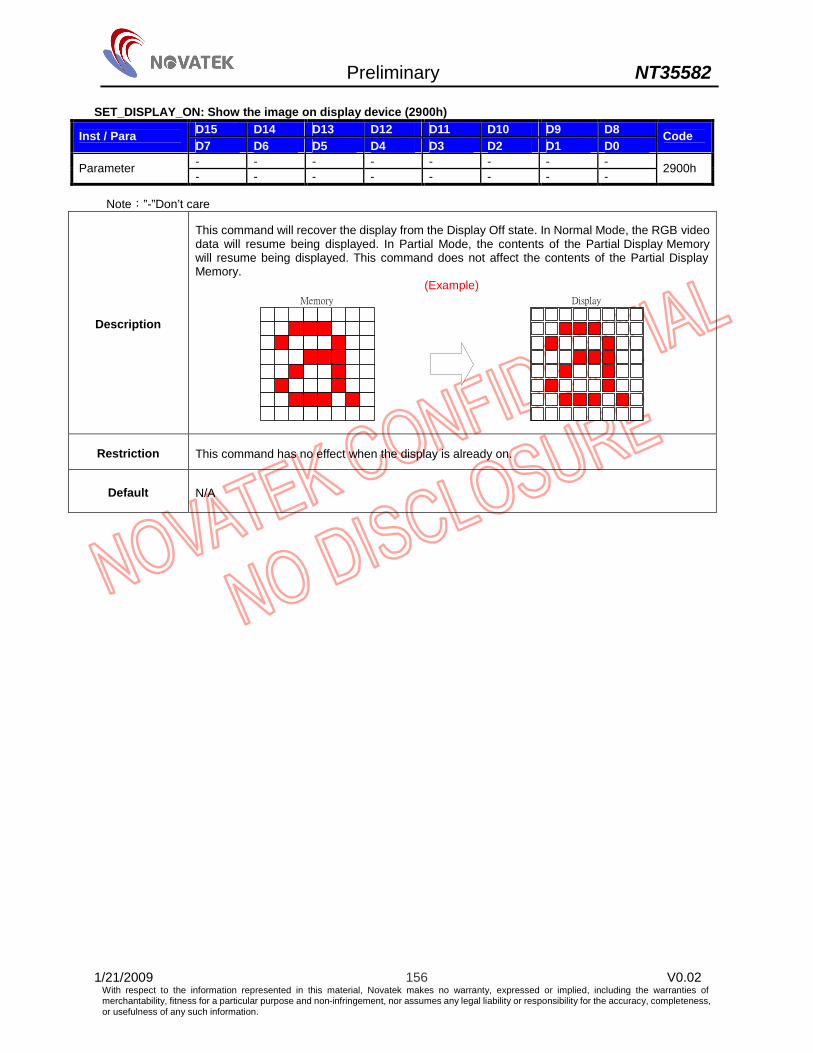
Preliminary NT35582
1/21/2009 156 V0.02 With respect to the information represented in this material, Novatek makes no warranty, expressed or implied, including the warranties of merchantability, fitness for a particular purpose and non-infringement, nor assumes any legal liability or responsibility for the accuracy, completeness, or usefulness of any such information.
SET_DISPLAY_ON: Show the image on display device (2900h) D15 D14 D13 D12 D11 D10 D9 D8 Inst / Para D7 D6 D5 D4 D3 D2 D1 D0
Code
- - - - - - - - Parameter - - - - - - - -
2900h
Note:”-”Don’t care
Description
This command will recover the display from the Display Off state. In Normal Mode, the RGB video data will resume being displayed. In Partial Mode, the contents of the Partial Display Memory will resume being displayed. This command does not affect the contents of the Partial Display Memory.
(Example) Memory Display
Restriction This command has no effect when the display is already on.
Default N/A
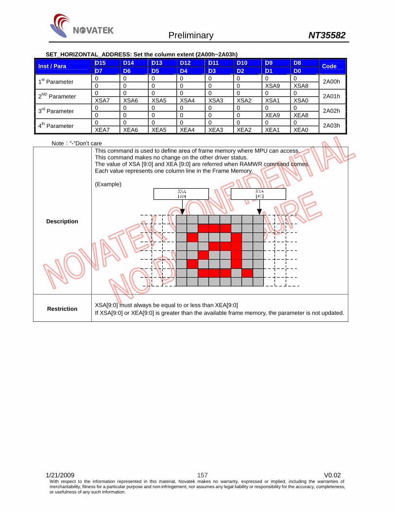
Preliminary NT35582
1/21/2009 157 V0.02 With respect to the information represented in this material, Novatek makes no warranty, expressed or implied, including the warranties of merchantability, fitness for a particular purpose and non-infringement, nor assumes any legal liability or responsibility for the accuracy, completeness, or usefulness of any such information.
SET_HORIZONTAL_ADDRESS: Set the column extent (2A00h~2A03h) D15 D14 D13 D12 D11 D10 D9 D8 Inst / Para D7 D6 D5 D4 D3 D2 D1 D0
Code
0 0 0 0 0 0 0 0 1st Parameter 0 0 0 0 0 0 XSA9 XSA8
2A00h
0 0 0 0 0 0 0 0 2ND Parameter XSA7 XSA6 XSA5 XSA4 XSA3 XSA2 XSA1 XSA0
2A01h
0 0 0 0 0 0 0 0 3rd Parameter 0 0 0 0 0 0 XEA9 XEA8
2A02h
0 0 0 0 0 0 0 0 4th Parameter XEA7 XEA6 XEA5 XEA4 XEA3 XEA2 XEA1 XEA0
2A03h
Note:”-”Don’t care
Description
This command is used to define area of frame memory where MPU can access. This command makes no change on the other driver status. The value of XSA [9:0] and XEA [9:0] are referred when RAMWR command comes. Each value represents one column line in the Frame Memory. (Example)
Restriction XSA[9:0] must always be equal to or less than XEA[9:0] If XSA[9:0] or XEA[9:0] is greater than the available frame memory, the parameter is not updated.
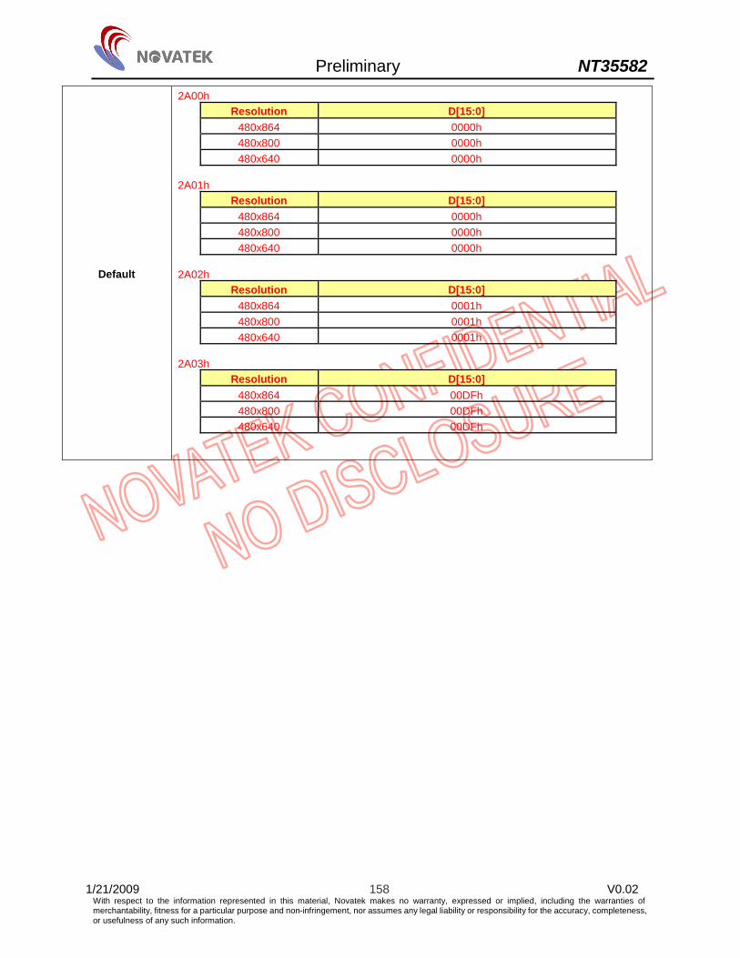
Preliminary NT35582
1/21/2009 158 V0.02 With respect to the information represented in this material, Novatek makes no warranty, expressed or implied, including the warranties of merchantability, fitness for a particular purpose and non-infringement, nor assumes any legal liability or responsibility for the accuracy, completeness, or usefulness of any such information.
Default
2A00h Resolution D[15:0]
480x864 0000h 480x800 0000h 480x640 0000h
2A01h
Resolution D[15:0] 480x864 0000h 480x800 0000h 480x640 0000h
2A02h
Resolution D[15:0] 480x864 0001h 480x800 0001h 480x640 0001h
2A03h
Resolution D[15:0] 480x864 00DFh 480x800 00DFh 480x640 00DFh
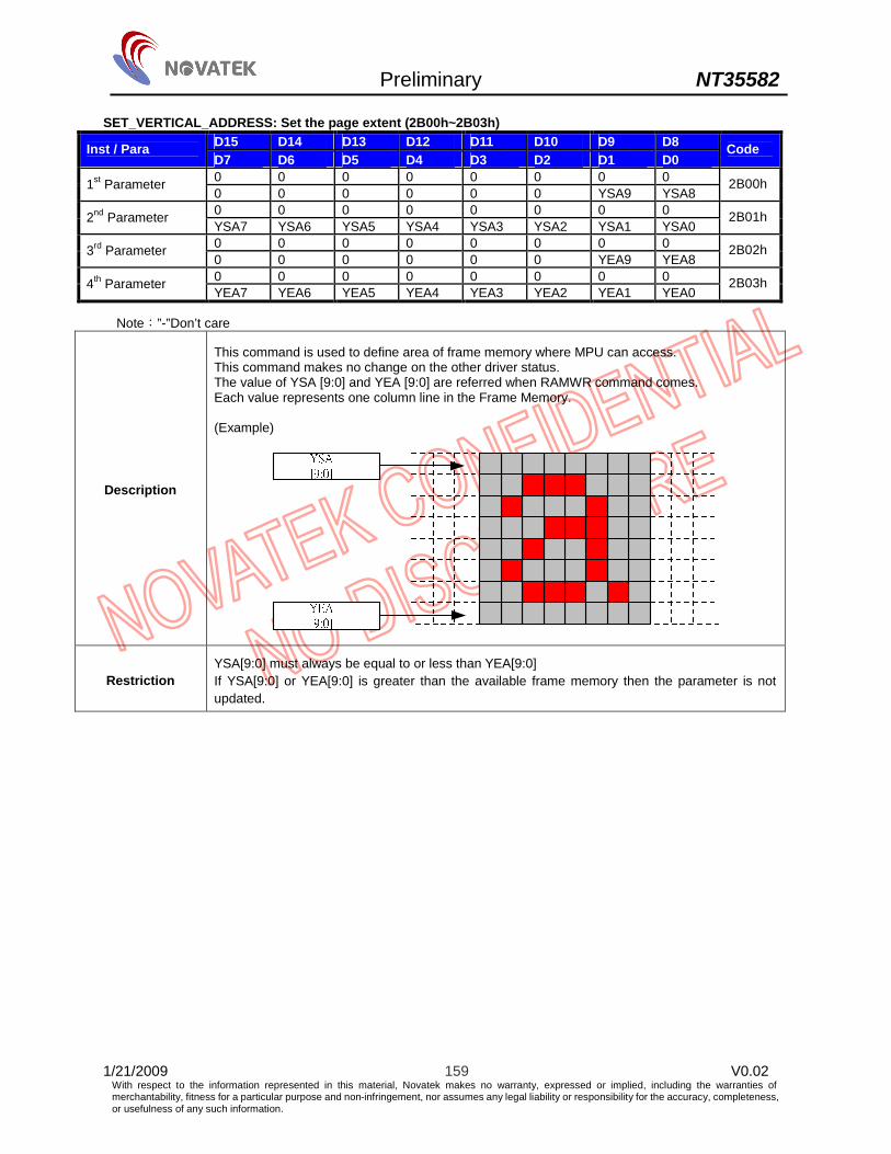
Preliminary NT35582
1/21/2009 159 V0.02 With respect to the information represented in this material, Novatek makes no warranty, expressed or implied, including the warranties of merchantability, fitness for a particular purpose and non-infringement, nor assumes any legal liability or responsibility for the accuracy, completeness, or usefulness of any such information.
SET_VERTICAL_ADDRESS: Set the page extent (2B00h~2B03h) D15 D14 D13 D12 D11 D10 D9 D8 Inst / Para D7 D6 D5 D4 D3 D2 D1 D0
Code
0 0 0 0 0 0 0 0 1st Parameter 0 0 0 0 0 0 YSA9 YSA8
2B00h
0 0 0 0 0 0 0 0 2nd Parameter YSA7 YSA6 YSA5 YSA4 YSA3 YSA2 YSA1 YSA0
2B01h
0 0 0 0 0 0 0 0 3rd Parameter 0 0 0 0 0 0 YEA9 YEA8
2B02h
0 0 0 0 0 0 0 0 4th Parameter YEA7 YEA6 YEA5 YEA4 YEA3 YEA2 YEA1 YEA0
2B03h
Note:”-”Don’t care
Description
This command is used to define area of frame memory where MPU can access. This command makes no change on the other driver status. The value of YSA [9:0] and YEA [9:0] are referred when RAMWR command comes. Each value represents one column line in the Frame Memory. (Example)
Restriction YSA[9:0] must always be equal to or less than YEA[9:0] If YSA[9:0] or YEA[9:0] is greater than the available frame memory then the parameter is not updated.

Preliminary NT35582
1/21/2009 160 V0.02 With respect to the information represented in this material, Novatek makes no warranty, expressed or implied, including the warranties of merchantability, fitness for a particular purpose and non-infringement, nor assumes any legal liability or responsibility for the accuracy, completeness, or usefulness of any such information.
Default
2B00h Resolution D[15:0]
480x864 0000h 480x800 0000h 480x640 0000h
2B01h
Resolution D[15:0] 480x864 0000h 480x800 0000h 480x640 0000h
2B02h
Resolution D[15:0] 480x864 0003h 480x800 0003h 480x640 0002h
2B03h
Resolution D[15:0] 480x864 005Fh 480x800 001Fh 480x640 007Fh

Preliminary NT35582
1/21/2009 161 V0.02 With respect to the information represented in this material, Novatek makes no warranty, expressed or implied, including the warranties of merchantability, fitness for a particular purpose and non-infringement, nor assumes any legal liability or responsibility for the accuracy, completeness, or usefulness of any such information.
WRITE_MEMORY_START: Memory Write Command (2C00h) D15 D14 D13 D12 D11 D10 D9 D8 Inst / Para D7 D6 D5 D4 D3 D2 D1 D0
Code
0 0 1 0 1 1 0 0 WRITE_MEMORY _START 0 0 0 0 0 0 0 0
2C00h
D15 D14 D13 D12 D11 D10 D9 D8 1st Parameter D7 D6 D5 D4 D3 D2 D1 D0
: : : : : : : : : D15 D14 D13 D12 D11 D10 D9 D8 Nth parameter D7 D6 D5 D4 D3 D2 D1 D0
Note:”-”Don’t care
Description This command writes data into the partial memory. It initializes the memory write address pointer to the start of the memory. Frame pointer auto-increments when data is written.
Restriction
A WRITE_MEMORY_START should follow a SET_COLUMN_ADDRESS, SET_PAGE_ADDRESS or SET_ADDRESS_MODE to define the write location. Otherwise, data written with WRITE_MEMORY_START and any following WRITE_MEMORY_CONTINUE commands is written to undefined locations. This command is used for CPU, SPI & MDDI interface.
Default N/A

Preliminary NT35582
1/21/2009 162 V0.02 With respect to the information represented in this material, Novatek makes no warranty, expressed or implied, including the warranties of merchantability, fitness for a particular purpose and non-infringement, nor assumes any legal liability or responsibility for the accuracy, completeness, or usefulness of any such information.
SET_RAM_ADDRESS: Set the RAM horizontal and vertical address (2D00h~2D03h) D15 D14 D13 D12 D11 D10 D9 D8 Inst / Para D7 D6 D5 D4 D3 D2 D1 D0
Code
0 0 0 0 0 0 0 0 1st Parameter 0 0 0 0 0 0 XAD9 XAD8
2D00h
0 0 0 0 0 0 0 0 2ND Parameter XAD7 XAD6 XAD5 XAD4 XAD3 XAD2 XAD1 XAD0
2D01h
0 0 0 0 0 0 0 0 3rd Parameter 0 0 0 0 0 0 YAD9 YAD8
2D02h
0 0 0 0 0 0 0 0 4th Parameter YAD7 YAD6 YAD5 YAD4 YAD3 YAD2 YAD1 YAD0
2D03h
Note:”-”Don’t care
Description
XAD[9:0], YAD[9:0]: A RAM address, which is set initially in the AC (Address Counter). T he NT35582 writes data to the internal RAM so that data is written consecutively without resetting the address in the AC. The address is not automatically updated when reading data from the internal RAM.
YAD[9:0] : XAD[9:0] RAM Data Setting 20’h000:000 – 20’h000:1DF Bitmap data on the 1st line 20’h001:000 – 20’h001:1DF Bitmap data on the 2nd line 20’h002:000 – 20’h002:1DF Bitmap data on the 3rd line 20’h003:000 – 20’h003:1DF Bitmap data on the 4th line 20’h004:000 – 20’h004:1DF Bitmap data on the 5th line : : 20’h35C:000 – 20’h35C:1DF Bitmap data on the 860th line 20’h35D:000 – 20’h35D:1DF Bitmap data on the 861st line 20’h35E:000 – 20’h35E:1DF Bitmap data on the 862nd line 20’h35F:000 – 20’h35F:1DF Bitmap data on the 863rd line
Restriction -

Preliminary NT35582
1/21/2009 163 V0.02 With respect to the information represented in this material, Novatek makes no warranty, expressed or implied, including the warranties of merchantability, fitness for a particular purpose and non-infringement, nor assumes any legal liability or responsibility for the accuracy, completeness, or usefulness of any such information.
Default
2D00h D15 D14 D13 D12 D11 D10 D09 D08
0 0 0 0 0 0 0 0 D07 D06 D05 D04 D03 D02 D01 D00
0 0 0 0 0 0 0 0 2D01h
D15 D14 D13 D12 D11 D10 D09 D08 0 0 0 0 0 0 0 0
D07 D06 D05 D04 D03 D02 D01 D00 0 0 0 0 0 0 0 0
2D02h
D15 D14 D13 D12 D11 D10 D09 D08 0 0 0 0 0 0 0 0
D07 D06 D05 D04 D03 D02 D01 D00 0 0 0 0 0 0 0 0
2D03h
D15 D14 D13 D12 D11 D10 D09 D08 0 0 0 0 0 0 0 0
D07 D06 D05 D04 D03 D02 D01 D00 0 0 0 0 0 0 0 0

Preliminary NT35582
1/21/2009 164 V0.02 With respect to the information represented in this material, Novatek makes no warranty, expressed or implied, including the warranties of merchantability, fitness for a particular purpose and non-infringement, nor assumes any legal liability or responsibility for the accuracy, completeness, or usefulness of any such information.
READ_MEMORY_START: Memory Read (2E00h) D15 D14 D13 D12 D11 D10 D9 D8 Inst / Para D7 D6 D5 D4 D3 D2 D1 D0
Code
0 0 1 0 1 1 1 0 READ_MEMORY _START 0 0 0 0 0 0 0 0
2E00h
D15 D14 D13 D12 D11 D10 D9 D8 1st Parameter D7 D6 D5 D4 D3 D2 D1 D0
: : : : : : : : : D15 D14 D13 D12 D11 D10 D9 D8 Nth Parameter D7 D6 D5 D4 D3 D2 D1 D0
Note:”-”Don’t care
Description This command is used to transfer data from frame memory to MPU.
Restriction -
Default N/A
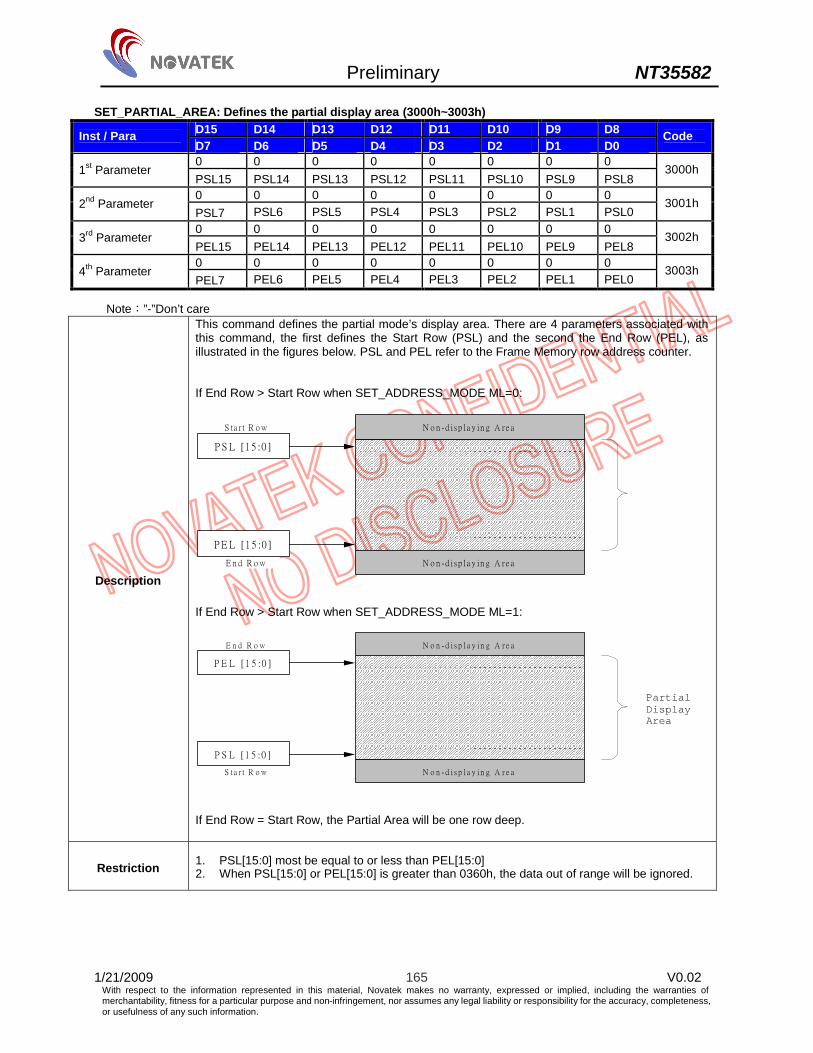
Preliminary NT35582
1/21/2009 165 V0.02 With respect to the information represented in this material, Novatek makes no warranty, expressed or implied, including the warranties of merchantability, fitness for a particular purpose and non-infringement, nor assumes any legal liability or responsibility for the accuracy, completeness, or usefulness of any such information.
SET_PARTIAL_AREA: Defines the partial display area (3000h~3003h) D15 D14 D13 D12 D11 D10 D9 D8 Inst / Para D7 D6 D5 D4 D3 D2 D1 D0
Code
0 0 0 0 0 0 0 0 1st Parameter
PSL15 PSL14 PSL13 PSL12 PSL11 PSL10 PSL9 PSL8 3000h
0 0 0 0 0 0 0 0 2nd Parameter
PSL7 PSL6 PSL5 PSL4 PSL3 PSL2 PSL1 PSL0 3001h
0 0 0 0 0 0 0 0 3rd Parameter
PEL15 PEL14 PEL13 PEL12 PEL11 PEL10 PEL9 PEL8 3002h
0 0 0 0 0 0 0 0 4th Parameter
PEL7 PEL6 PEL5 PEL4 PEL3 PEL2 PEL1 PEL0 3003h
Note:”-”Don’t care
Description
This command defines the partial mode’s display area. There are 4 parameters associated with this command, the first defines the Start Row (PSL) and the second the End Row (PEL), as illustrated in the figures below. PSL and PEL refer to the Frame Memory row address counter. If End Row > Start Row when SET_ADDRESS_MODE ML=0:
S ta r t R o w
E n d R o w
N o n -d isp la y in g A re a
N o n -d isp la y in g A re a
P S L [1 5 :0 ]
P E L [1 5 :0 ]
If End Row > Start Row when SET_ADDRESS_MODE ML=1:
E n d R o w
S ta r t R o w
N o n - d i s p l a y in g A r e a
N o n - d i s p l a y in g A r e a
P E L [ 1 5 :0 ]
P S L [ 1 5 :0 ]
If End Row = Start Row, the Partial Area will be one row deep.
Restriction 1. PSL[15:0] most be equal to or less than PEL[15:0] 2. When PSL[15:0] or PEL[15:0] is greater than 0360h, the data out of range will be ignored.
Partial Display Area
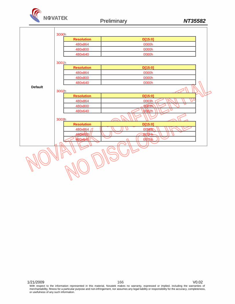
Preliminary NT35582
1/21/2009 166 V0.02 With respect to the information represented in this material, Novatek makes no warranty, expressed or implied, including the warranties of merchantability, fitness for a particular purpose and non-infringement, nor assumes any legal liability or responsibility for the accuracy, completeness, or usefulness of any such information.
Default
3000h Resolution D[15:0]
480x864 0000h 480x800 0000h 480x640 0000h
3001h
Resolution D[15:0] 480x864 0000h 480x800 0000h 480x640 0000h
3002h
Resolution D[15:0] 480x864 0003h 480x800 0003h 480x640 0002h
3003h
Resolution D[15:0] 480x864 005Fh 480x800 001Fh 480x640 007Fh

Preliminary NT35582
1/21/2009 167 V0.02 With respect to the information represented in this material, Novatek makes no warranty, expressed or implied, including the warranties of merchantability, fitness for a particular purpose and non-infringement, nor assumes any legal liability or responsibility for the accuracy, completeness, or usefulness of any such information.
SET_TEAR_OFF: Tearing Effect Line OFF (3400h) D15 D14 D13 D12 D11 D10 D9 D8 Inst / Para D7 D6 D5 D4 D3 D2 D1 D0
Code
- - - - - - - - Parameter - - - - - - - -
3400h
Note:”-”Don’t care
Description This command is used to turn OFF (Active Low) the output TE trigger message from the display module.
Restriction This command has no effect when TE is already OFF.
Default N/A
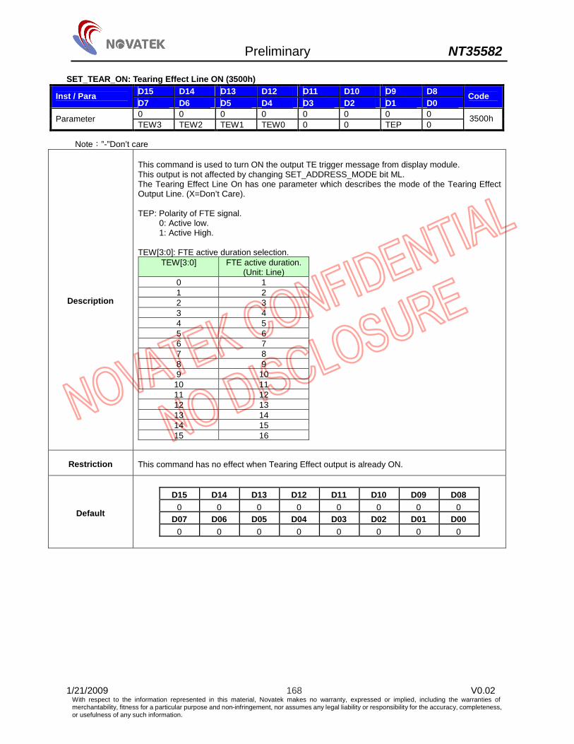
Preliminary NT35582
1/21/2009 168 V0.02 With respect to the information represented in this material, Novatek makes no warranty, expressed or implied, including the warranties of merchantability, fitness for a particular purpose and non-infringement, nor assumes any legal liability or responsibility for the accuracy, completeness, or usefulness of any such information.
SET_TEAR_ON: Tearing Effect Line ON (3500h) D15 D14 D13 D12 D11 D10 D9 D8 Inst / Para D7 D6 D5 D4 D3 D2 D1 D0
Code
0 0 0 0 0 0 0 0 Parameter TEW3 TEW2 TEW1 TEW0 0 0 TEP 0
3500h
Note:”-”Don’t care
Description
This command is used to turn ON the output TE trigger message from display module. This output is not affected by changing SET_ADDRESS_MODE bit ML. The Tearing Effect Line On has one parameter which describes the mode of the Tearing Effect Output Line. (X=Don’t Care). TEP: Polarity of FTE signal. 0: Active low. 1: Active High. TEW[3:0]: FTE active duration selection.
TEW[3:0] FTE active duration. (Unit: Line)
0 1 1 2 2 3 3 4 4 5 5 6 6 7 7 8 8 9 9 10
10 11 11 12 12 13 13 14 14 15 15 16
Restriction This command has no effect when Tearing Effect output is already ON.
Default
D15 D14 D13 D12 D11 D10 D09 D08 0 0 0 0 0 0 0 0
D07 D06 D05 D04 D03 D02 D01 D00 0 0 0 0 0 0 0 0

Preliminary NT35582
1/21/2009 169 V0.02 With respect to the information represented in this material, Novatek makes no warranty, expressed or implied, including the warranties of merchantability, fitness for a particular purpose and non-infringement, nor assumes any legal liability or responsibility for the accuracy, completeness, or usefulness of any such information.
SET_ADDRESS_MODE: Set the read order from frame memory (3600h~3601h) D15 D14 D13 D12 D11 D10 D9 D8 Inst / Para D7 D6 D5 D4 D3 D2 D1 D0
Code
0 0 0 0 0 0 0 0 Parameter MY MX MV 0 RGB 0 CRL CTB
3600h
0 0 0 0 0 0 0 0 Parameter 0 0 0 0 0 0 0 HSM
3601h
Note:”-”Don’t care
Description
This command defines read/write scanning direction of frame memory. This command makes no change on the other driver status.
Bit NAME DESCRIPTION MY Row Address Order MX Column Address Order MV Row/Column Exchange
These 3bits control MPU to memory write/read direction.
RGB RGB-BGR Order Color selector switch control (0=RGB color filter panel, 1=BGR color filter panel)
CRL Horizontal refresh order & Display change LCD horizontal refresh direction control & display change
CTB Vertical Refresh Order & Display change LCD vertical refresh direction control & display change
Memory Display
Memory Display
CTB=1
CTB: Vertical refresh Order & Display change
Top- Left (0,0)Top- Left (0,0)
Top- Left (0,0)Top- Left (0,0)
G1
Gn
G2
G1
Gn
G2
TB(pin)=H
CTB=0
TB(pin)=L
CTB=0
TB(pin)=H
CTB=1
TB(pin)=L

Preliminary NT35582
1/21/2009 170 V0.02 With respect to the information represented in this material, Novatek makes no warranty, expressed or implied, including the warranties of merchantability, fitness for a particular purpose and non-infringement, nor assumes any legal liability or responsibility for the accuracy, completeness, or usefulness of any such information.
BGR
SIG1
Driver IC
BGR
SIG1 SIG2
BGR
BGR BGR
SIG2
BGR
SIG132
SIG132
BGR
BGR
LCD Panel
B G R
SIG1
Driver ICSIG1 SIG2
SIG2
SIG132
SIG132
LCD Panel
B G R
B G R
B G R
B G R
B G R
B G R
B G R
RGB="0" RGB="1"
RGB: RGB-BGR Order
Display
MemoryMemory
Display
CRL: Horizontal refresh Order & Display change
Top- Left (0,0)
Top- Left (0,0)
Top- Left (0,0)
Top- Left (0,0)
S1 SnS2 S1 SnS2
CRL=1
RL(pin)=H
CRL=0
RL(pin)=L
CRL=1
RL(pin)=H
CRL=0
RL(pin)=L
HSM: This instruction bit enables the NT35582 writing data to GRAM at high speed.
HSM 0 1 RAM write mode Normal RAM write High speed RAM write
Restriction This command has no effect when TE is already OFF.
Default
D15 D14 D13 D12 D11 D10 D09 D08 0 0 0 0 0 0 0 0
D07 D06 D05 D04 D03 D02 D01 D00 0 0 0 0 0 0 0 0
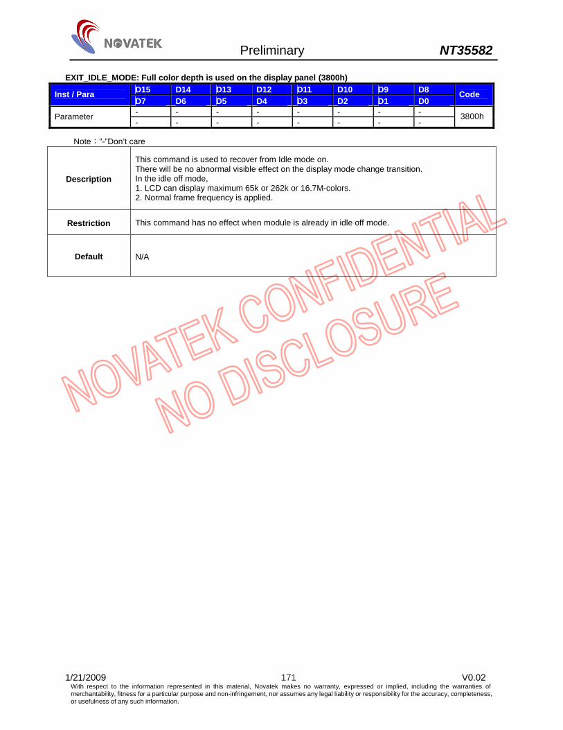
Preliminary NT35582
1/21/2009 171 V0.02 With respect to the information represented in this material, Novatek makes no warranty, expressed or implied, including the warranties of merchantability, fitness for a particular purpose and non-infringement, nor assumes any legal liability or responsibility for the accuracy, completeness, or usefulness of any such information.
EXIT_IDLE_MODE: Full color depth is used on the display panel (3800h) D15 D14 D13 D12 D11 D10 D9 D8 Inst / Para D7 D6 D5 D4 D3 D2 D1 D0
Code
- - - - - - - - Parameter - - - - - - - -
3800h
Note:”-”Don’t care
Description
This command is used to recover from Idle mode on. There will be no abnormal visible effect on the display mode change transition. In the idle off mode, 1. LCD can display maximum 65k or 262k or 16.7M-colors. 2. Normal frame frequency is applied.
Restriction This command has no effect when module is already in idle off mode.
Default N/A

Preliminary NT35582
1/21/2009 172 V0.02 With respect to the information represented in this material, Novatek makes no warranty, expressed or implied, including the warranties of merchantability, fitness for a particular purpose and non-infringement, nor assumes any legal liability or responsibility for the accuracy, completeness, or usefulness of any such information.
ENTER_IDLE_MODE: Reduced color depth is used on the display panel (3900h) D15 D14 D13 D12 D11 D10 D9 D8 Inst / Para D7 D6 D5 D4 D3 D2 D1 D0
Code
- - - - - - - - Parameter - - - - - - - -
3900h
Note:”-”Don’t care
Description
This command is used to enter into Idle mode on. There will be no abnormal visible effect on the display mode change transition. In the idle on mode, 1.Color expression is reduced. The primary and the secondary colors using MSB of each RMG
and B in the Frame Memory, 8 color depth data is displayed. 2.8-Color mode frame frequency is applied. 3.Exit from IDMON by Idle Mode Off (3800h) command (Example)
Memory Display
Restriction This command has no effect when module is already in idle On mode.
Default N/A

Preliminary NT35582
1/21/2009 173 V0.02 With respect to the information represented in this material, Novatek makes no warranty, expressed or implied, including the warranties of merchantability, fitness for a particular purpose and non-infringement, nor assumes any legal liability or responsibility for the accuracy, completeness, or usefulness of any such information.
SET_PIXEL_FORMAT: Set how many bits per pixel are used (3A00h) D15 D14 D13 D12 D11 D10 D9 D8 Inst / Para D7 D6 D5 D4 D3 D2 D1 D0
Code
0 0 0 0 0 0 0 0 Parameter 0 VIPF2 VIPF1 VIPF0 0 IFPF2 IFPF1 IFPF0
3A00h
Note:”-”Don’t care
Description
This command is used to define the format of RGB picture data, which is to be transferred via the MPU Interface. The formats are shown in the table: IFPF[2:0]: Set the pixel format on MCU I/F
IFPF[2:0] MCU Interface Color Format
101 5 16-bits/pixel
110 6 18-bits/pixel
111 7 24-bits/pixel
Others are not define VIPF[2:0] : set the pixel format on RGB I/F
VIPF[2:0] RGB Interface Color Format
101 5 16 bits/pixel (1-time transfer)
110 6 18 bits/pixel (1-time transfer)
111 7 24 bits/pixel (1-time transfer)
Others are not define
Restriction There is no visible effect until the Frame Memory is written to.
Default
D15 D14 D13 D12 D11 D10 D09 D08 0 0 0 0 0 0 0 0
D07 D06 D05 D04 D03 D02 D01 D00 0 1 1 1 0 1 1 1
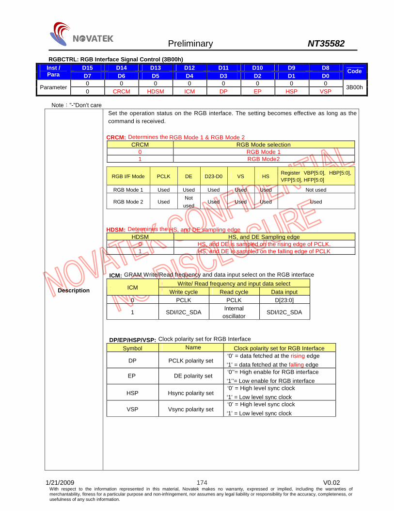
Preliminary NT35582
1/21/2009 174 V0.02 With respect to the information represented in this material, Novatek makes no warranty, expressed or implied, including the warranties of merchantability, fitness for a particular purpose and non-infringement, nor assumes any legal liability or responsibility for the accuracy, completeness, or usefulness of any such information.
RGBCTRL: RGB Interface Signal Control (3B00h) D15 D14 D13 D12 D11 D10 D9 D8 Inst /
Para D7 D6 D5 D4 D3 D2 D1 D0 Code
0 0 0 0 0 0 0 0 Parameter
0 CRCM HDSM ICM DP EP HSP VSP 3B00h
Note:”-”Don’t care
Description
Set the operation status on the RGB interface. The setting becomes effective as long as the command is received.
CRCM: Determines the RGB Mode 1 & RGB Mode 2 CRCM RGB Mode selection
0 RGB Mode 1 1 RGB Mode2
RGB I/F Mode PCLK DE D23-D0 VS HS Register VBP[5:0], HBP[5:0], VFP[5:0], HFP[5:0]
RGB Mode 1 Used Used Used Used Used Not used
RGB Mode 2 Used Not used Used Used Used Used
HDSM: Determines the HS, and DE sampling edge HDSM HS, and DE Sampling edge
0 HS, and DE is sampled on the rising edge of PCLK. 1 HS, and DE is sampled on the falling edge of PCLK
ICM: GRAM Write/Read frequency and data input select on the RGB interface
Write/ Read frequency and input data select ICM
Write cycle Read cycle Data input 0 PCLK PCLK D[23:0]
1 SDI/I2C_SDA Internal
oscillator SDI/I2C_SDA
DP/EP/HSP/VSP: Clock polarity set for RGB Interface
Symbol Name Clock polarity set for RGB Interface
DP PCLK polarity set ‘0’ = data fetched at the rising edge ‘1’ = data fetched at the falling edge
EP DE polarity set ‘0’’= High enable for RGB interface ‘1’’= Low enable for RGB interface
HSP Hsync polarity set ‘0’ = High level sync clock ‘1’ = Low level sync clock
VSP Vsync polarity set ‘0’ = High level sync clock ‘1’ = Low level sync clock

Preliminary NT35582
1/21/2009 175 V0.02 With respect to the information represented in this material, Novatek makes no warranty, expressed or implied, including the warranties of merchantability, fitness for a particular purpose and non-infringement, nor assumes any legal liability or responsibility for the accuracy, completeness, or usefulness of any such information.
Restriction -
Default
D15 D14 D13 D12 D11 D10 D09 D08
0 0 0 0 0 0 0 0 D07 D06 D05 D04 D03 D02 D01 D00
0 0 0 0 0 0 1 1

Preliminary NT35582
1/21/2009 176 V0.02 With respect to the information represented in this material, Novatek makes no warranty, expressed or implied, including the warranties of merchantability, fitness for a particular purpose and non-infringement, nor assumes any legal liability or responsibility for the accuracy, completeness, or usefulness of any such information.
RGBPRCTR: RGB Interface Blanking Porch setting (3B02h~3B05h) D15 D14 D13 D12 D11 D10 D9 D8 Inst /
Para D7 D6 D5 D4 D3 D2 D1 D0 Code
0 0 0 0 0 0 0 0 Parameter
0 0 VBP5 VBP4 VBP3 VBP2 VBP1 VBP0 3B02h
0 0 0 0 0 0 0 0 Parameter 0 0 VFP5 VFP4 VFP3 VFP2 VFP1 VFP0
3B03h
0 0 0 0 0 0 0 0 Parameter 0 0 HBP5 HBP4 HBP3 HBP2 HBP1 HBP0
3B04h
0 0 0 0 0 0 0 0 Parameter 0 0 HFP5 HFP4 HFP3 HFP2 HFP1 HFP0
3B05h
Note:”-”Don’t care
Description
Vertical and Horizontal back and front porch control when RGB I/F mode 2 only. VBP[5:0]: number of lines for the back porch of VSYNC.
VBP[5:0] No. of clock cycle of HSYNC 00d 1 01d 2 02d 3 03d 4
: : :
: (STEP 1)
: 62d 63 63d 64
VFP[5:0]: number of lines for the front porch of VSYNC.
VFP[5:0] No. of clock cycle of HSYNC 00d 1 01d 2 02d 3 03d 4
: : :
: (STEP 1)
: 62d 63 63d 64
HBP[5:0]: number of clock for the back porch of HSYNC.
HBP[5:0] No. of clock cycle of PCLK 00d 1 01d 2 02d 3 03d 4
: : :
: (STEP 1)
: 62d 63 63d 64

Preliminary NT35582
1/21/2009 177 V0.02 With respect to the information represented in this material, Novatek makes no warranty, expressed or implied, including the warranties of merchantability, fitness for a particular purpose and non-infringement, nor assumes any legal liability or responsibility for the accuracy, completeness, or usefulness of any such information.
HFP[5:0]: number of clock for the front porch of HSYNC. HFP[5:0] No. of clock cycle of PCLK
00d 1 01d 2 02d 3 03d 4
: : :
: (STEP 1)
: 62d 63 63d 64
Restriction - Vporch: VBP≧5H line, VFP≧2H line
Default
3B02h:
D15 D14 D13 D12 D11 D10 D09 D08 0 0 0 0 0 0 0 0
D07 D06 D05 D04 D03 D02 D01 D00 0 0 0 0 0 1 0 1
3B03h:
D15 D14 D13 D12 D11 D10 D09 D08 0 0 0 0 0 0 0 0
D07 D06 D05 D04 D03 D02 D01 D00 0 0 0 0 0 0 1 0
3B04h:
D15 D14 D13 D12 D11 D10 D09 D08 0 0 0 0 0 0 0 0
D07 D06 D05 D04 D03 D02 D01 D00 0 0 0 0 0 0 1 0
3B05h:
D15 D14 D13 D12 D11 D10 D09 D08 0 0 0 0 0 0 0 0
D07 D06 D05 D04 D03 D02 D01 D00 0 0 0 0 0 0 1 0

Preliminary NT35582
1/21/2009 178 V0.02 With respect to the information represented in this material, Novatek makes no warranty, expressed or implied, including the warranties of merchantability, fitness for a particular purpose and non-infringement, nor assumes any legal liability or responsibility for the accuracy, completeness, or usefulness of any such information.
SET_TEAR_SCANLINE: Set Tear Line (4400h~4401h) D15 D14 D13 D12 D11 D10 D9 D8 Inst / Para D7 D6 D5 D4 D3 D2 D1 D0
Code
0 0 0 0 0 0 0 0 1st Parameter 0 0 0 0 0 0 N9 N8
4400h
0 0 0 0 0 0 0 0 2nd Parameter N7 N6 N5 N4 N3 N2 N1 N0
4401h
Note:”-”Don’t care
Description
This command is used to set the FTE output position. Use “SET_TEAR_ON (3500h)” to set the FTE polarity and pulse width.
N[9:0] FTE output line 10’h00 1st line 10’h01 2nd line 10’h02 3rd line : : 10h36D 878th line 10’h36E 879th line 10’h36F 880th line
Restriction This command takes affect on the frame following the current frame. Therefore, if the Tear Effect (FTE) output is already ON, the FTE output shall continue to operate as programmed by the previous SET_TEAR_ON, or SET_TEAR_SCANLINE, command until the end of the frame.
Default
4400h: D15 D14 D13 D12 D11 D10 D09 D08
0 0 0 0 0 0 0 0 D07 D06 D05 D04 D03 D02 D01 D00
0 0 0 0 0 0 0 0 4401h:
D15 D14 D13 D12 D11 D10 D09 D08 0 0 0 0 0 0 0 0
D07 D06 D05 D04 D03 D02 D01 D00 0 0 0 0 0 0 0 0

Preliminary NT35582
1/21/2009 179 V0.02 With respect to the information represented in this material, Novatek makes no warranty, expressed or implied, including the warranties of merchantability, fitness for a particular purpose and non-infringement, nor assumes any legal liability or responsibility for the accuracy, completeness, or usefulness of any such information.
SET_IM3: IM3 setting by software in serial interface operation (4D00h) D15 D14 D13 D12 D11 D10 D9 D8 Inst /
Para D7 D6 D5 D4 D3 D2 D1 D0 Code
0 0 0 0 0 0 0 0 Parameter
0 0 0 0 0 0 0 CIM3 4D00h
Note:”-”Don’t care
Description
This command only is used to set the SCL rising or falling edge trigger in related SPI interface operation by software setting. For Serial interface, RGB+SPI interface & MDDI + SPI interface setting only.
CIM3 SCL trigger edge 0 Rising edge 1 Falling edge
Restriction This command can only set by using MDDI interface.
Default
D15 D14 D13 D12 D11 D10 D09 D08
0 0 0 0 0 0 0 0 D07 D06 D05 D04 D03 D02 D01 D00
0 0 0 0 0 0 0 0

Preliminary NT35582
1/21/2009 180 V0.02 With respect to the information represented in this material, Novatek makes no warranty, expressed or implied, including the warranties of merchantability, fitness for a particular purpose and non-infringement, nor assumes any legal liability or responsibility for the accuracy, completeness, or usefulness of any such information.
SPI_I2C_SEL: SPI or I2C interface operation selection in MDDI+SPI/I2C mode (4E00h) D15 D14 D13 D12 D11 D10 D9 D8 Inst /
Para D7 D6 D5 D4 D3 D2 D1 D0 Code
0 0 0 0 0 0 0 0 Parameter
0 0 0 0 0 0 0 SPI_I2C 4E00h
Note:”-”Don’t care
Description
This command only is used to set the SPI or I2C interface operation in MDDI + SPI/I2C mode control for IM2_0 pin equal to “101”. SPI_I2C =0: MDDI + SPI interface. (IM2_0 = “101”) SPI_I2C =1: MDDI + I2C interface. (IM2_0 = “101”)
Restriction This command can only set by using MDDI interface.
Default
D15 D14 D13 D12 D11 D10 D09 D08
0 0 0 0 0 0 0 0 D07 D06 D05 D04 D03 D02 D01 D00
0 0 0 0 0 0 0 0

Preliminary NT35582
1/21/2009 181 V0.02 With respect to the information represented in this material, Novatek makes no warranty, expressed or implied, including the warranties of merchantability, fitness for a particular purpose and non-infringement, nor assumes any legal liability or responsibility for the accuracy, completeness, or usefulness of any such information.
DSTB_SET: Enter Deep Standby mode (4F00h) D15 D14 D13 D12 D11 D10 D9 D8 Inst /
Para D7 D6 D5 D4 D3 D2 D1 D0 Code
0 0 0 0 0 0 0 0 Parameter
0 0 0 0 0 0 0 DSTB 4F00h
Note:”-”Don’t care
Description
This command is used to enter/exit deep standby mode. DSTB = 1:enter deep standby mode Note: (1) Before setting this command, remember to enter “Sleep In mode” first. (2) Set DSTB = 0 can’t exit deep standby mode Note for exit deep standby mode:
a. To exit deep standby mode, please refer the following sequence. 1): Input 1KHz square waveform to CSX pin. 2): Keep the square waveform larger than 6mS.
b. Or set RESET to exit deep standby mode
Restriction -
Default
D15 D14 D13 D12 D11 D10 D09 D08 0 0 0 0 0 0 0 0
D07 D06 D05 D04 D03 D02 D01 D00 0 0 0 0 0 0 0 0

Preliminary NT35582
1/21/2009 182 V0.02 With respect to the information represented in this material, Novatek makes no warranty, expressed or implied, including the warranties of merchantability, fitness for a particular purpose and non-infringement, nor assumes any legal liability or responsibility for the accuracy, completeness, or usefulness of any such information.
WRPFD: Write Profile Values for Display (5000h~500Fh) D15 D14 D13 D12 D11 D10 D9 D8 Inst / Para D7 D6 D5 D4 D3 D2 D1 D0
Code
0 0 0 0 0 0 0 0 Parameter STEP_OUT
_DP0[7] STEP_OUT
_DP0[6] STEP_OUT
_DP0[5] STEP_OUT
_DP0[4] STEP_OUT
_DP0[3] STEP_OUT
_DP0[2] STEP_OUT
_DP0[1] STEP_OUT
_DP0[0] 5000h
0 0 0 0 0 0 0 0 Parameter STEP_OUT
_DP1[7] STEP_OUT
_DP1[6] STEP_OUT
_DP1[5] STEP_OUT
_DP1[4] STEP_OUT
_DP1[3] STEP_OUT
_DP1[2] STEP_OUT
_DP1[1] STEP_OUT
_DP1[0] 5001h
0 0 0 0 0 0 0 0 Parameter STEP_OUT
_DP2[7] STEP_OUT
_DP2[6] STEP_OUT
_DP2[5] STEP_OUT
_DP2[4] STEP_OUT
_DP2[3] STEP_OUT
_DP2[2] STEP_OUT
_DP2[1] STEP_OUT
_DP2[0] 5002h
0 0 0 0 0 0 0 0 Parameter STEP_OUT
_DP3[7] STEP_OUT
_DP3[6] STEP_OUT
_DP3[5] STEP_OUT
_DP3[4] STEP_OUT
_DP3[3] STEP_OUT
_DP3[2] STEP_OUT
_DP3[1] STEP_OUT
_DP3[0] 5003h
0 0 0 0 0 0 0 0 Parameter STEP_OUT
_DP4[7] STEP_OUT
_DP4[6] STEP_OUT
_DP4[5] STEP_OUT
_DP4[4] STEP_OUT
_DP4[3] STEP_OUT
_DP4[2] STEP_OUT
_DP4[1] STEP_OUT
_DP4[0] 5004h
0 0 0 0 0 0 0 0 Parameter STEP_OUT
_DP5[7] STEP_OUT
_DP5[6] STEP_OUT
_DP5[5] STEP_OUT
_DP5[4] STEP_OUT
_DP5[3] STEP_OUT
_DP5[2] STEP_OUT
_DP5[1] STEP_OUT
_DP5[0] 5005h
0 0 0 0 0 0 0 0 Parameter STEP_OUT
_DP6[7] STEP_OUT
_DP6[6] STEP_OUT
_DP6[5] STEP_OUT
_DP6[4] STEP_OUT
_DP6[3] STEP_OUT
_DP6[2] STEP_OUT
_DP6[1] STEP_OUT
_DP6[0] 5006h
0 0 0 0 0 0 0 0 Parameter STEP_OUT
_DP7[7] STEP_OUT
_DP7[6] STEP_OUT
_DP7[5] STEP_OUT
_DP7[4] STEP_OUT
_DP7[3] STEP_OUT
_DP7[2] STEP_OUT
_DP7[1] STEP_OUT
_DP7[0] 5007h
0 0 0 0 0 0 0 0 Parameter STEP_OUT
_DP8[7] STEP_OUT
_DP8[6] STEP_OUT
_DP8[5] STEP_OUT
_DP8[4] STEP_OUT
_DP8[3] STEP_OUT
_DP8[2] STEP_OUT
_DP8[1] STEP_OUT
_DP8[0] 5008h
0 0 0 0 0 0 0 0 Parameter STEP_OUT
_DP9[7] STEP_OUT
_DP9[6] STEP_OUT
_DP9[5] STEP_OUT
_DP9[4] STEP_OUT
_DP9[3] STEP_OUT
_DP9[2] STEP_OUT
_DP9[1] STEP_OUT
_DP9[0] 5009h
0 0 0 0 0 0 0 0 Parameter STEP_OUT
_DP10[7] STEP_OUT_DP10[6]
STEP_OUT_DP10[5]
STEP_OUT_DP10[4]
STEP_OUT_DP10[3]
STEP_OUT_DP10[2]
STEP_OUT_DP10[1]
STEP_OUT_DP10[0]
500Ah 0 0 0 0 0 0 0 0
Parameter STEP_OUT_DP11[7]
STEP_OUT_DP11[6]
STEP_OUT_DP11[5]
STEP_OUT_DP11[4]
STEP_OUT_DP11[3]
STEP_OUT_DP11[2]
STEP_OUT_DP11[1]
STEP_OUT_DP11[0]
500Bh 0 0 0 0 0 0 0 0
Parameter STEP_OUT_DP12[7]
STEP_OUT_DP12[6]
STEP_OUT_DP12[5]
STEP_OUT_DP12[4]
STEP_OUT_DP12[3]
STEP_OUT_DP12[2]
STEP_OUT_DP12[1]
STEP_OUT_DP12[0]
500Ch 0 0 0 0 0 0 0 0
Parameter STEP_OUT_DP13[7]
STEP_OUT_DP13[6]
STEP_OUT_DP13[5]
STEP_OUT_DP13[4]
STEP_OUT_DP13[3]
STEP_OUT_DP13[2]
STEP_OUT_DP13[1]
STEP_OUT_DP13[0]
500Dh 0 0 0 0 0 0 0 0
Parameter STEP_OUT_DP14[7]
STEP_OUT_DP14[6]
STEP_OUT_DP14[5]
STEP_OUT_DP14[4]
STEP_OUT_DP14[3]
STEP_OUT_DP14[2]
STEP_OUT_DP14[1]
STEP_OUT_DP14[0]
500Eh 0 0 0 0 0 0 0 0
Parameter STEP_OUT_DP15[7]
STEP_OUT_DP15[6]
STEP_OUT_DP15[5]
STEP_OUT_DP15[4]
STEP_OUT_DP15[3]
STEP_OUT_DP15[2]
STEP_OUT_DP15[1]
STEP_OUT_DP15[0]
500Fh
Note:”-”Don’t care
Description This command is used to define Profile Values for display.
Restriction -
Default
5000h~500Fh D15 D14 D13 D12 D11 D10 D09 D08
0 0 0 0 0 0 0 0 D07 D06 D05 D04 D03 D02 D01 D00
1 1 1 1 1 1 1 1
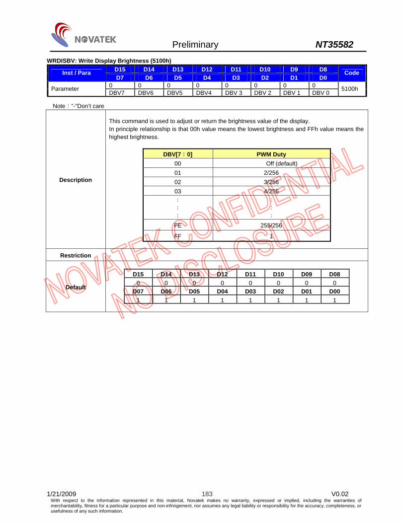
Preliminary NT35582
1/21/2009 183 V0.02 With respect to the information represented in this material, Novatek makes no warranty, expressed or implied, including the warranties of merchantability, fitness for a particular purpose and non-infringement, nor assumes any legal liability or responsibility for the accuracy, completeness, or usefulness of any such information.
WRDISBV: Write Display Brightness (5100h) D15 D14 D13 D12 D11 D10 D9 D8 Inst / Para D7 D6 D5 D4 D3 D2 D1 D0
Code
0 0 0 0 0 0 0 0 Parameter DBV7 DBV6 DBV5 DBV4 DBV 3 DBV 2 DBV 1 DBV 0
5100h
Note:”-”Don’t care
Description
This command is used to adjust or return the brightness value of the display. In principle relationship is that 00h value means the lowest brightness and FFh value means the highest brightness.
DBV[7:0] PWM Duty 00 Off (default) 01 2/256 02 3/256 03 4/256 : : :
: : :
FE 255/256
FF 1
Restriction -
Default
D15 D14 D13 D12 D11 D10 D09 D08 0 0 0 0 0 0 0 0
D07 D06 D05 D04 D03 D02 D01 D00 1 1 1 1 1 1 1 1
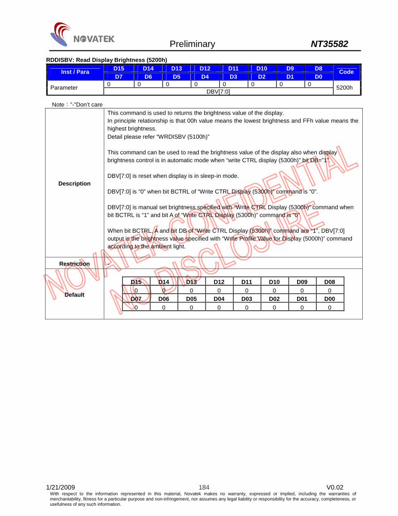
Preliminary NT35582
1/21/2009 184 V0.02 With respect to the information represented in this material, Novatek makes no warranty, expressed or implied, including the warranties of merchantability, fitness for a particular purpose and non-infringement, nor assumes any legal liability or responsibility for the accuracy, completeness, or usefulness of any such information.
RDDISBV: Read Display Brightness (5200h) D15 D14 D13 D12 D11 D10 D9 D8 Inst / Para D7 D6 D5 D4 D3 D2 D1 D0
Code
0 0 0 0 0 0 0 0 Parameter DBV[7:0]
5200h
Note:”-”Don’t care
Description
This command is used to returns the brightness value of the display. In principle relationship is that 00h value means the lowest brightness and FFh value means the highest brightness. Detail please refer “WRDISBV (5100h)” This command can be used to read the brightness value of the display also when display brightness control is in automatic mode when “write CTRL display (5300h)” bit DB=”1”. DBV[7:0] is reset when display is in sleep-in mode. DBV[7:0] is “0” when bit BCTRL of “Write CTRL Display (5300h)” command is “0”. DBV[7:0] is manual set brightness specified with “Write CTRL Display (5300h)” command when bit BCTRL is “1” and bit A of “Write CTRL Display (5300h)” command is “0” When bit BCTRL, A and bit DB of “Write CTRL Display (5300h)” command are “1”, DBV[7:0] output is the brightness value specified with “Write Profile Value for Display (5000h)” command according to the ambient light.
Restriction -
Default
D15 D14 D13 D12 D11 D10 D09 D08 0 0 0 0 0 0 0 0
D07 D06 D05 D04 D03 D02 D01 D00 0 0 0 0 0 0 0 0

Preliminary NT35582
1/21/2009 185 V0.02 With respect to the information represented in this material, Novatek makes no warranty, expressed or implied, including the warranties of merchantability, fitness for a particular purpose and non-infringement, nor assumes any legal liability or responsibility for the accuracy, completeness, or usefulness of any such information.
WRCTRLD: Write CTRL Display (5300h) D15 D14 D13 D12 D11 D10 D9 D8 Inst / Para D7 D6 D5 D4 D3 D2 D1 D0
Code
0 0 0 0 0 0 0 0 Parameter
0 0 BCTRL A DD BL 0 0 5300h
Note:”-”Don’t care
Description
This command is used to control the “LEDPWM” pin, dimming function for CABC, ambient light sensing, and LABC mode switching. BCTRL: Turn On/Off the brightness control block with the dimming effect. About the register “LEDPWPOL”, please refer to the register “CTRLEDPWM (5301h)”
BCTRL LEDPWPOL LEDPWM Pin Final State Backlight
Final State 0 0 Keep “LOW” (0% PWM Duty) (Default) OFF 1 0 PWM Output (High level is duty) ON 0 1 Keep “HIGH” (0% PWM Duty) OFF
1 1 Inversed PWM Output (Low level is duty) ON A:This command is used to control ambient light, brightness and gamma settings.
A Ambient Light Sensing
0 OFF (Ambient Light Sensing OFF) (Default)
1 ON (Ambient Light Sensing ON) DD: Enable/Disable dimming function only for CABC.
DD CABC Dimming Function
0 Disabled
1 Enabled (Default) BL: Turn On/Off the backlight control without dimming effect.
BL Backlight Control 0 OFF (Default)
1 ON When BL bit change from “1” to “0”, backlight is turned off without gradual dimming, even if dimming-on (DD = “1”) are selected.
Restriction -
Default
D15 D14 D13 D12 D11 D10 D09 D08
0 0 0 0 0 0 0 0 D07 D06 D05 D04 D03 D02 D01 D00
0 0 0 0 1 0 0 0

Preliminary NT35582
1/21/2009 186 V0.02 With respect to the information represented in this material, Novatek makes no warranty, expressed or implied, including the warranties of merchantability, fitness for a particular purpose and non-infringement, nor assumes any legal liability or responsibility for the accuracy, completeness, or usefulness of any such information.
CTRLEDPWM: Set the States for LED Control Pins (5301h) D15 D14 D13 D12 D11 D10 D9 D8 Inst / Para D7 D6 D5 D4 D3 D2 D1 D0
Code
0 0 0 0 0 0 0 0 Parameter
0 0 0 PWM_ENH_OE
CLED_VOL
LEDPWPOL
LEDONPOL
LEDONR
5301h
Note:”-”Don’t care
Description
This command is used to set states for LED control pins. LEDONR: Turn On/Off the LEDON pin
LEDONR LEDONPOL LEDON Pin Final State
0 0 Keep “LOW” (Default) 1 0 Keep “HIGH” 0 1 Keep “HIGH”
1 1 Keep “LOW” LEDPWPOL: Set the PWM active polarity for external LED driver control
Polarity of LEDPWM Pin LEDPWPOL
Lit period Non-lit-period 0 High Low 1 Low High
In other words, LEDPWPOL = “1” is suitable setting for “Low-Active” LED driver IC. LEDONPOL: Set the enable active polarity for external LED driver control
Polarity of LEDON Pin LEDONPOL
Lit period Non-lit-period 0 High Low 1 Low High
In other words, LEDONPOL = “1” is suitable setting for “Low-Active” LED driver IC. CLED_VOL: Set the logic voltage level for LEDPWM and LEDON pins
CLED_VOL Logic Voltage Level for LEDPWM and LEDON
0 LEDPWM: Logic voltage level is VDDIO <-> 0V LEDON: Logic voltage level is VDDIO <-> 0V
1 LEDPWM: Logic voltage level is VCI <-> 0V LEDON: Logic voltage level is VCI <-> 0V
PWM_ENH_OE: This setting is used to enhance the driving ability of “LEDPWM” pin.
PWM_ENH_OE Logic Voltage Level for LEDPWM and LEDON 0 1X driving ability of LEDPWM pin (Default) 1 2X driving ability of LEDPWM pin
Restriction -
Default
D15 D14 D13 D12 D11 D10 D09 D08 0 0 0 0 0 0 0 0
D07 D06 D05 D04 D03 D02 D01 D00 0 0 0 0 0 0 0 0

Preliminary NT35582
1/21/2009 187 V0.02 With respect to the information represented in this material, Novatek makes no warranty, expressed or implied, including the warranties of merchantability, fitness for a particular purpose and non-infringement, nor assumes any legal liability or responsibility for the accuracy, completeness, or usefulness of any such information.
CTRLDIM_L: Turn On/Off the Dimming Function for LABC (5302h) D15 D14 D13 D12 D11 D10 D9 D8 Inst / Para D7 D6 D5 D4 D3 D2 D1 D0
Code
0 0 0 0 0 0 0 0 Parameter
0 0 0 0 0 0 0 DDL 5302h
Note:”-”Don’t care
Description
This command is used to disable/enable the dimming function for LABC DDL: Turn On/Off the dimming function for LABC
DDL Dimming Function for LABC
0 Disable
1 Enable (Default)
Restriction -
Default
D15 D14 D13 D12 D11 D10 D09 D08 0 0 0 0 0 0 0 0
D07 D06 D05 D04 D03 D02 D01 D00 0 0 0 0 0 0 0 1

Preliminary NT35582
1/21/2009 188 V0.02 With respect to the information represented in this material, Novatek makes no warranty, expressed or implied, including the warranties of merchantability, fitness for a particular purpose and non-infringement, nor assumes any legal liability or responsibility for the accuracy, completeness, or usefulness of any such information.
DIMPRDIN_L: Set the Rising Dimming Style for LABC (5303h) D15 D14 D13 D12 D11 D10 D9 D8 Inst / Para D7 D6 D5 D4 D3 D2 D1 D0
Code
0 0 0 0 0 0 0 0 Parameter
SEL_IN 0 0 0 DM_IN[3 : 0] 5303h
Note:”-”Don’t care
Description
This command is used to set the rising dimming for LABC dimming function SEL_IN: Set the rising dimming type for LABC
SEL_IN Dimming Style For Rising Dimming
0 “Fixed Time” Type
1 “Fixed Slope” Type DM_IN[3 : 0]: Set the each dimming step time for rising dimming condition.
DM_IN[3 : 0] Rising Dimming Step Time 0x00 1 Frame (Default) 0x01 2 Frames 0x02 3 Frames 0x03 4 Frames 0x04 5 Frames 0x05 6 Frames 0x06 7 Frames
0x07 8 Frames
0x08 Reserved : :
Reserved
0x0F Reserved
PWM
Dut
y (%
)
PWM
Dut
y (%
)
When dimming style is set as “ Fixed Time” type, the total dimming time length of rising dimming process is equal to DMSTP_L × DM_IN, the unit of total dimming time is “Frame”. For example: DMSTP_L[2 : 0] is set 0x06, this means that the total dimming steps are 128 steps DM_IN[3 : 0] is set 0x03, this means that each dimming step time length of rising dimming is 4 frames. So, the total dimming time length is 512 frames ( = 128 x 4)
Restriction -

Preliminary NT35582
1/21/2009 189 V0.02 With respect to the information represented in this material, Novatek makes no warranty, expressed or implied, including the warranties of merchantability, fitness for a particular purpose and non-infringement, nor assumes any legal liability or responsibility for the accuracy, completeness, or usefulness of any such information.
Default
D15 D14 D13 D12 D11 D10 D09 D08 0 0 0 0 0 0 0 0
D07 D06 D05 D04 D03 D02 D01 D00 0 0 0 0 0 0 0 0

Preliminary NT35582
1/21/2009 190 V0.02 With respect to the information represented in this material, Novatek makes no warranty, expressed or implied, including the warranties of merchantability, fitness for a particular purpose and non-infringement, nor assumes any legal liability or responsibility for the accuracy, completeness, or usefulness of any such information.
DIMPRDDE_L: Set the Falling Dimming Style for LABC (5304h) D15 D14 D13 D12 D11 D10 D9 D8 Inst / Para D7 D6 D5 D4 D3 D2 D1 D0
Code
0 0 0 0 0 0 0 0 Parameter SEL_D
E 0 0 0 DM_DE[3 : 0] 5304h
Note:”-”Don’t care
Description
This command is used to set the falling dimming for LABC dimming function SEL_DE: Set the falling dimming type for LABC
SEL_DE Dimming Style For Falling Dimming
0 “Fixed Time” Type
1 “Fixed Slope” Type DM_DE[3 : 0]: Set the each dimming step time for falling dimming condition.
DM_DE[3 : 0] Falling Dimming Step Time
0x00 1 Frame (Default) 0x01 2 Frames 0x02 3 Frames 0x03 4 Frames 0x04 5 Frames 0x05 6 Frames 0x06 7 Frames
0x07 8 Frames
0x08 Reserved : :
Reserved
0x0F Reserved
PWM
Dut
y (%
)
PWM
Dut
y (%
)
When dimming style is set as “ Fixed Time” type, the total dimming time length of falling dimming process is equal to DMSTP_L × DM_DE, the unit of total dimming time is “Frame”. For example: DMSTP_L[2 : 0] is set 0x03, this means that the total dimming steps are 16 steps DM_DE[3 : 0] is set 0x04, this means that each dimming step time length of falling dimming is 5 frames. So, the total dimming time length is 80 frames ( = 16 x 5)
Restriction -
Preliminary NT35582
1/21/2009 191 V0.02 With respect to the information represented in this material, Novatek makes no warranty, expressed or implied, including the warranties of merchantability, fitness for a particular purpose and non-infringement, nor assumes any legal liability or responsibility for the accuracy, completeness, or usefulness of any such information.
Default
D15 D14 D13 D12 D11 D10 D09 D08 0 0 0 0 0 0 0 0
D07 D06 D05 D04 D03 D02 D01 D00 0 0 0 0 0 0 0 0

Preliminary NT35582
1/21/2009 192 V0.02 With respect to the information represented in this material, Novatek makes no warranty, expressed or implied, including the warranties of merchantability, fitness for a particular purpose and non-infringement, nor assumes any legal liability or responsibility for the accuracy, completeness, or usefulness of any such information.
DMSTP_L: Set the Total Dimming Steps for LABC (5305h) D15 D14 D13 D12 D11 D10 D9 D8 Inst / Para D7 D6 D5 D4 D3 D2 D1 D0
Code
0 0 0 0 0 0 0 0 Parameter
0 0 0 0 0 DMSTP_L[2 : 0] 5305h
Note:”-”Don’t care
Description
This command is used to set total steps for rising dimming and falling dimming DMSTP_L[2 : 0]: Set the dimming steps for rising dimming and falling dimming
DMSTP_L[2 : 0] Total Steps Per Dimming Procedure
0x00 2 Steps
0x01 4 Steps
0x02 8 Steps
0x03 16 Steps
0x04 32 Steps (Default)
0x05 64 Steps
0x06 128 Steps
0x07 256 Steps
PWM
Dut
y (%
)
PWM
Dut
y (%
)
Note: When dimming type is set “Fixed Time” type, the “DMSTP_L[2 : 0]” setting is available. For example: DMSTP_L[2 : 0] is set 0x07, this means that the total dimming steps are 256 steps DM_DE[3 : 0] is set 0x01, this means that each dimming step time length of falling dimming is 2 frames. So, the total dimming time length is 512 frames ( = 256 x 2)
Restriction -
Default
D15 D14 D13 D12 D11 D10 D09 D08 0 0 0 0 0 0 0 0
D07 D06 D05 D04 D03 D02 D01 D00 0 0 0 0 0 1 0 0

Preliminary NT35582
1/21/2009 193 V0.02 With respect to the information represented in this material, Novatek makes no warranty, expressed or implied, including the warranties of merchantability, fitness for a particular purpose and non-infringement, nor assumes any legal liability or responsibility for the accuracy, completeness, or usefulness of any such information.
DMFIXSP_L: Set the Fixed Increasing / Decreasing PWM Duty Steps of LABC (5306h) D15 D14 D13 D12 D11 D10 D9 D8 Inst / Para D7 D6 D5 D4 D3 D2 D1 D0
Code
0 0 0 0 0 0 0 0 Parameter
STEP_DE[3 : 0] STEP_IN[3 : 0] 5306h
Note:”-”Don’t care
Description
This command is used to set increasing / decreasing PWM duty steps of LABC. STEP_IN[3:0]: Set the increasing PWM duty steps for rising dimming process.
STEP_DE[3:0] Total Steps Per Dimming Procedure
0x00 Reserved
0x01 1 (Default)
0x02 2
0x03 3
0x04 4
0x05 5
0x06 6
0x07 7 : :
: :
0x0E 14
0x0F 15 STEP_DE[3:0]: Set the decreasing PWM duty steps for falling dimming process.
STEP_IN[3:0] Total Steps Per Dimming Procedure
0x00 Reserved
0x01 1 (Default)
0x02 2
0x03 3
0x04 4
0x05 5
0x06 6
0x07 7 : :
: :
0x0E 14
0x0F 15
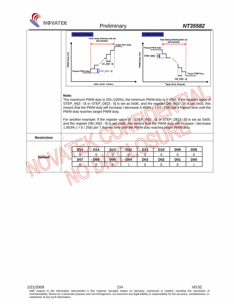
Preliminary NT35582
1/21/2009 194 V0.02 With respect to the information represented in this material, Novatek makes no warranty, expressed or implied, including the warranties of merchantability, fitness for a particular purpose and non-infringement, nor assumes any legal liability or responsibility for the accuracy, completeness, or usefulness of any such information.
PWM
Dut
y (%
)
PWM
Dut
y (%
)
Note: The maximum PWM duty is 255 (100%), the minimum PWM duty is 0 (0%). If the register value of STEP_IN[3 : 0] or STEP_DE[3 : 0] is set as 0x0E, and the register DM_IN[3 : 0] is set 0x03, this means that the PWM duty will increase / decrease 5.468% ( = 14 / 256) per 4 frames time until the PWM duty reaches target PWM duty. For another example: If the register value of STEP_IN[3 : 0] or STEP_DE[3 : 0] is set as 0x05, and the register DM_IN[3 : 0] is set 0x06, this means that the PWM duty will increase / decrease 1.953% ( = 5 / 256) per 7 frames time until the PWM duty reaches target PWM duty.
Restriction -
Default
D15 D14 D13 D12 D11 D10 D09 D08 0 0 0 0 0 0 0 0
D07 D06 D05 D04 D03 D02 D01 D00 0 0 0 1 0 0 0 1

Preliminary NT35582
1/21/2009 195 V0.02 With respect to the information represented in this material, Novatek makes no warranty, expressed or implied, including the warranties of merchantability, fitness for a particular purpose and non-infringement, nor assumes any legal liability or responsibility for the accuracy, completeness, or usefulness of any such information.
DMSPSTILL_C: Set the Total Dimming Steps for Still-Mode of CABC (5307h) D15 D14 D13 D12 D11 D10 D9 D8 Inst / Para D7 D6 D5 D4 D3 D2 D1 D0
Code
0 0 0 0 0 0 0 0 Parameter
0 0 0 0 0 DIM_STEP_STILL[2 : 0] 5307h
Note:”-”Don’t care
Description
This command is used to set total dimming steps for Still-Mode of CABC. DIM_STEP_STILL[2:0]: Set the total dimming steps for Still-Mode
DIM_STEP_STILL[2:0] Total Steps Per Dimming Procedure
0x00 2
0x01 4 (Default)
0x02 8
0x03 16
0x04 32
0x05 64
0x06 128
0x07 256 Backlight dimming in Still-Mode:
PWM
Dut
y (%
)
PWM
Dut
y (%
)
Note: Rising dimming and falling dimming for Still-Mode of CABC are using the same registers (DIM_STEP_STILL[2:0] and DMST_C[3:0]) to set the total dimming steps and each dimming step time. For example: DIM_STEP_STILL[2 : 0] is set 0x06, this means that the total dimming steps are 128 steps DMST_C[3 : 0] is set 0x01, this means that each dimming step time length of falling dimming is 2 frames. So, the total dimming time length is 256 frames ( = 128 x 2)
Restriction -
Default
D15 D14 D13 D12 D11 D10 D09 D08 0 0 0 0 0 0 0 0
D07 D06 D05 D04 D03 D02 D01 D00 0 0 0 0 0 0 0 1

Preliminary NT35582
1/21/2009 196 V0.02 With respect to the information represented in this material, Novatek makes no warranty, expressed or implied, including the warranties of merchantability, fitness for a particular purpose and non-infringement, nor assumes any legal liability or responsibility for the accuracy, completeness, or usefulness of any such information.
DMSPMOV_C: Set the Total Dimming Steps for Moving-Mode of CABC (5308h) D15 D14 D13 D12 D11 D10 D9 D8 Inst / Para D7 D6 D5 D4 D3 D2 D1 D0
Code
0 0 0 0 0 0 0 0 Parameter
0 0 0 0 0 DIM_STEP_MOV[2 : 0] 5308h
Note:”-”Don’t care
Description
This command is used to set total dimming steps for Moving-Mode of CABC. DIM_STEP_MOV[2 : 0]: Set the total dimming steps for Moving-Mode
DIM_STEP_MOV[2 : 0] Total Steps Per Dimming Procedure 0x00 2
0x01 4
0x02 8
0x03 16
0x04 32 (Default)
0x05 64
0x06 128
0x07 256 Backlight dimming in Moving-Mode:
PWM
Dut
y (%
)
PWM
Dut
y (%
)
Note: Rising dimming and falling dimming for Moving-Mode of CABC are using the same registers (DIM_STEP_MOV[2 : 0] and DMST_C[3 : 0]) to set the total dimming steps and each dimming step time. For example: DIM_STEP_MOV[2 : 0] is set 0x01, this means that the total dimming steps are 4 steps DMST_C[3 : 0] is set 0x05, this means that each dimming step time length of falling dimming is 6 frames. So, the total dimming time length is 24 frames ( = 4 x 6)
Restriction -
Default
D15 D14 D13 D12 D11 D10 D09 D08 0 0 0 0 0 0 0 0
D07 D06 D05 D04 D03 D02 D01 D00 0 0 0 0 0 1 0 0
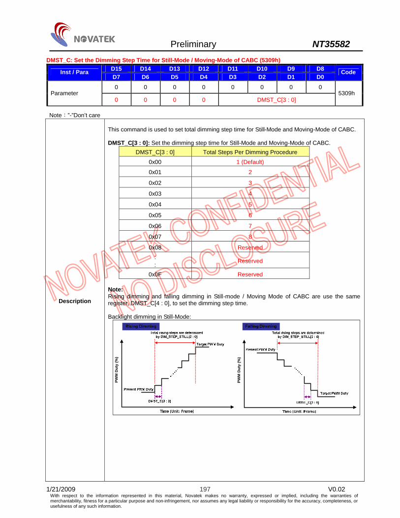
Preliminary NT35582
1/21/2009 197 V0.02 With respect to the information represented in this material, Novatek makes no warranty, expressed or implied, including the warranties of merchantability, fitness for a particular purpose and non-infringement, nor assumes any legal liability or responsibility for the accuracy, completeness, or usefulness of any such information.
DMST_C: Set the Dimming Step Time for Still-Mode / Moving-Mode of CABC (5309h) D15 D14 D13 D12 D11 D10 D9 D8 Inst / Para D7 D6 D5 D4 D3 D2 D1 D0
Code
0 0 0 0 0 0 0 0 Parameter
0 0 0 0 DMST_C[3 : 0] 5309h
Note:”-”Don’t care
Description
This command is used to set total dimming step time for Still-Mode and Moving-Mode of CABC. DMST_C[3 : 0]: Set the dimming step time for Still-Mode and Moving-Mode of CABC.
DMST_C[3 : 0] Total Steps Per Dimming Procedure
0x00 1 (Default)
0x01 2
0x02 3
0x03 4
0x04 5
0x05 6
0x06 7
0x07 8
0x08 Reserved : :
Reserved
0x0F Reserved Note: Rising dimming and falling dimming in Still-mode / Moving Mode of CABC are use the same register, DMST_C[4 : 0], to set the dimming step time. Backlight dimming in Still-Mode:
PWM
Dut
y (%
)
PWM
Dut
y (%
)

Preliminary NT35582
1/21/2009 198 V0.02 With respect to the information represented in this material, Novatek makes no warranty, expressed or implied, including the warranties of merchantability, fitness for a particular purpose and non-infringement, nor assumes any legal liability or responsibility for the accuracy, completeness, or usefulness of any such information.
Backlight dimming in Moving-Mode:
PWM
Dut
y (%
)
PWM
Dut
y (%
)
For example 1: DIM_STEP_STILL[2 : 0] is set 0x06, this means that the total dimming steps are 128 steps DMST_C[3 : 0] is set 0x01, this means that each dimming step time length of falling dimming is 2 frames. So, the total dimming time length is 256 frames ( = 128 x 2) For example 2: DIM_STEP_MOV[2 : 0] is set 0x01, this means that the total dimming steps are 4 steps DMST_C[3 : 0] is set 0x05, this means that each dimming step time length of falling dimming is 6 frames. So, the total dimming time length is 24 frames ( = 4 x 6)
Restriction -
Default
D15 D14 D13 D12 D11 D10 D09 D08 0 0 0 0 0 0 0 0
D07 D06 D05 D04 D03 D02 D01 D00 0 0 0 0 0 0 0 0

Preliminary NT35582
1/21/2009 199 V0.02 With respect to the information represented in this material, Novatek makes no warranty, expressed or implied, including the warranties of merchantability, fitness for a particular purpose and non-infringement, nor assumes any legal liability or responsibility for the accuracy, completeness, or usefulness of any such information.
RDCTRLD: Read CTRL Display (5400h) D15 D14 D13 D12 D11 D10 D9 D8 Inst / Para D7 D6 D5 D4 D3 D2 D1 D0
Code
0 0 0 0 0 0 0 0 Parameter
0 0 BCTRL A DD BL 0 0 5400h
Note:”-”Don’t care
Description
This command is used to “read” the setting status of “LEDPWM” pin, dimming function for CABC, ambient light sensing, and LABC mode switching. BCTRL: On/Off status of the brightness control block. About the register “LEDPWPOL”, please refer to the register “CTRLEDPWM (5301h)”
BCTRL LEDPWPOL LEDPWM Pin Final State Backlight
Final State 0 0 Keep “LOW” (0% PWM Duty) OFF 1 0 PWM Output (High level is duty) ON 0 1 Keep “HIGH” (0% PWM Duty) OFF
1 1 Inversed PWM Output (Low level is duty) ON A:The status of ambient light sensing, brightness and gamma settings.
A Ambient Light Sensing 0 OFF (Ambient Light Sensing OFF)
1 ON (Ambient Light Sensing ON) DD: Enabled/Disabled status of dimming function only for CABC.
DD CABC Dimming Function
0 Disabled
1 Enabled BL: On/Off status of the backlight control.
BL Backlight Control
0 OFF
1 ON DB:Display brightness manual/automatic status for LABC
DB Display Brightness M/A Control of LABC
0 Manual
1 Automatic G:Gamma Manual/Automatic Status
G Gamma M/A Control
0 Manual
1 Automatic When BL bit change from “1” to “0”, backlight is turned off without gradual dimming, even if

Preliminary NT35582
1/21/2009 200 V0.02 With respect to the information represented in this material, Novatek makes no warranty, expressed or implied, including the warranties of merchantability, fitness for a particular purpose and non-infringement, nor assumes any legal liability or responsibility for the accuracy, completeness, or usefulness of any such information.
dimming-on (DD = “1”) are selected. When the ambient light sensing off-mode (A = “0”), display brightness and gamma setting should be manual setting (DB = “0” and G = “0”). Setting values are the last one written with “Write Display Brightness (5100h)” command and GAMSET-command or the default one. When the ambient light control on, light sensor control block is always working, even if backlight off (BL = “0”) and display brightness manual (DB = “0”) are selected.
Restriction Read Only
Default
D15 D14 D13 D12 D11 D10 D09 D08
0 0 0 0 0 0 0 0 D07 D06 D05 D04 D03 D02 D01 D00
0 0 0 0 1 0 0 0

Preliminary NT35582
1/21/2009 201 V0.02 With respect to the information represented in this material, Novatek makes no warranty, expressed or implied, including the warranties of merchantability, fitness for a particular purpose and non-infringement, nor assumes any legal liability or responsibility for the accuracy, completeness, or usefulness of any such information.
RDCTRLEDPWM: Read The Setting Status for LED Control Pins (5401h) D15 D14 D13 D12 D11 D10 D9 D8 Inst / Para D7 D6 D5 D4 D3 D2 D1 D0
Code
0 0 0 0 0 0 0 0 Parameter
0 0 0 PWM_ENH_OE
CLED_VOL
LEDPWPOL
LEDONPOL
LEDONR
5401h
Note:”-”Don’t care
Description
This command is used to “read” status for LED control pins setting. LEDONR: On/Off status of the LEDON pin
LEDONR LEDONPOL LEDON Pin Final State 0 0 Keep “LOW” 1 0 Keep “HIGH” 0 1 Keep “HIGH”
1 1 Keep “LOW” LEDPWPOL: PWM polarity setting status for LEDPWM pin
Polarity of LEDPWM Pin LEDPWPOL
Lit period Non-lit-period 0 High Low 1 Low High
In other words, LEDPWPOL = “1” is suitable setting for “Low-Active” LED driver IC. LEDONPOL: PWM polarity setting status for LEDON pin
Polarity of LEDON Pin LEDONPOL
Lit period Non-lit-period 0 High Low 1 Low High
In other words, LEDONPOL = “1” is suitable setting for “Low-Active” LED driver IC. CLED_VOL: Logic voltage level setting status for LEDPWM and LEDON pins
CLED_VOL Logic Voltage Level for LEDPWM and LEDON 0 LEDPWM: Logic voltage level is VDDIO <-> 0V
LEDON: Logic voltage level is VDDIO <-> 0V 1 LEDPWM: Logic voltage level is VCI <-> 0V
LEDON: Logic voltage level is VCI <-> 0V PWM_ENH_OE: Driving ability setting status of “LEDPWM” pin.
PWM_ENH_OE Logic Voltage Level for LEDPWM and LEDON 0 1X driving ability of LEDPWM pin 1 2X driving ability of LEDPWM pin
Restriction Read Only
Default
D15 D14 D13 D12 D11 D10 D09 D08 0 0 0 0 0 0 0 0
D07 D06 D05 D04 D03 D02 D01 D00 0 0 0 0 0 0 0 0

Preliminary NT35582
1/21/2009 202 V0.02 With respect to the information represented in this material, Novatek makes no warranty, expressed or implied, including the warranties of merchantability, fitness for a particular purpose and non-infringement, nor assumes any legal liability or responsibility for the accuracy, completeness, or usefulness of any such information.
RDCTRLDIM_L: Read The Dimming Function On/Off Status of LABC (5402h) D15 D14 D13 D12 D11 D10 D9 D8 Inst / Para D7 D6 D5 D4 D3 D2 D1 D0
Code
0 0 0 0 0 0 0 0 Parameter
0 0 0 0 0 0 0 DDL 5402h
Note:”-”Don’t care
Description
This command is used to “read” the On/Off status of the dimming function for LABC DDL: On/Off status of the dimming function for LABC
DDL Dimming Function for LABC
0 Disable
1 Enable (Default)
Restriction Read Only
Default
D15 D14 D13 D12 D11 D10 D09 D08 0 0 0 0 0 0 0 0
D07 D06 D05 D04 D03 D02 D01 D00 0 0 0 0 0 0 0 1

Preliminary NT35582
1/21/2009 203 V0.02 With respect to the information represented in this material, Novatek makes no warranty, expressed or implied, including the warranties of merchantability, fitness for a particular purpose and non-infringement, nor assumes any legal liability or responsibility for the accuracy, completeness, or usefulness of any such information.
RDDIMPRDIN_L: Read The Rising Dimming Setting For LABC (5403h) D15 D14 D13 D12 D11 D10 D9 D8 Inst / Para D7 D6 D5 D4 D3 D2 D1 D0
Code
0 0 0 0 0 0 0 0 Parameter
SEL_IN 0 0 0 DM_IN[3 : 0] 5403h
Note:”-”Don’t care
Description
This command is used to “read” the rising dimming setting for LABC dimming function SEL_IN: Rising dimming type for LABC
SEL_IN Dimming Style For Rising Dimming
0 “Fixed Time” Type
1 “Fixed Slope” Type DM_IN[3 : 0]: Read the setting about the each dimming step time for rising dimming condition.
DM_IN[3 : 0] Rising Dimming Step Time 0x00 1 Frame (Default) 0x01 2 Frames 0x02 3 Frames 0x03 4 Frames 0x04 5 Frames 0x05 6 Frames 0x06 7 Frames
0x07 8 Frames
0x08 Reserved : :
Reserved
0x0F Reserved
PWM
Dut
y (%
)
PWM
Dut
y (%
)
When dimming style is set as “ Fixed Time” type, the total dimming time length of rising dimming process is equal to DMSTP_L × DM_IN, the unit of total dimming time is “Frame”. For example: DMSTP_L[2 : 0] is set 0x06, this means that the total dimming steps are 128 steps DM_IN[3 : 0] is set 0x03, this means that each dimming step time length of rising dimming is 4 frames. So, the total dimming time length is 512 frames ( = 128 x 4)

Preliminary NT35582
1/21/2009 204 V0.02 With respect to the information represented in this material, Novatek makes no warranty, expressed or implied, including the warranties of merchantability, fitness for a particular purpose and non-infringement, nor assumes any legal liability or responsibility for the accuracy, completeness, or usefulness of any such information.
Restriction Read Only
Default
D15 D14 D13 D12 D11 D10 D09 D08 0 0 0 0 0 0 0 0
D07 D06 D05 D04 D03 D02 D01 D00 0 0 0 0 0 0 0 0
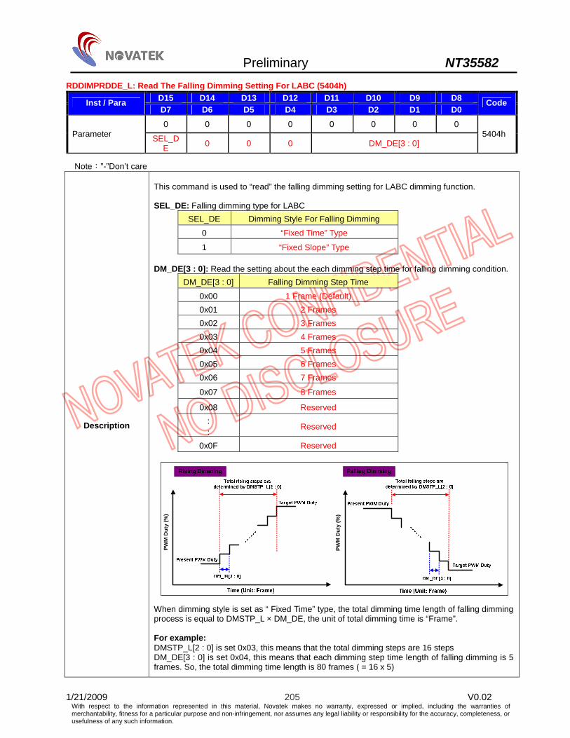
Preliminary NT35582
1/21/2009 205 V0.02 With respect to the information represented in this material, Novatek makes no warranty, expressed or implied, including the warranties of merchantability, fitness for a particular purpose and non-infringement, nor assumes any legal liability or responsibility for the accuracy, completeness, or usefulness of any such information.
RDDIMPRDDE_L: Read The Falling Dimming Setting For LABC (5404h) D15 D14 D13 D12 D11 D10 D9 D8 Inst / Para D7 D6 D5 D4 D3 D2 D1 D0
Code
0 0 0 0 0 0 0 0 Parameter SEL_D
E 0 0 0 DM_DE[3 : 0] 5404h
Note:”-”Don’t care
Description
This command is used to “read” the falling dimming setting for LABC dimming function. SEL_DE: Falling dimming type for LABC
SEL_DE Dimming Style For Falling Dimming
0 “Fixed Time” Type
1 “Fixed Slope” Type DM_DE[3 : 0]: Read the setting about the each dimming step time for falling dimming condition.
DM_DE[3 : 0] Falling Dimming Step Time
0x00 1 Frame (Default) 0x01 2 Frames 0x02 3 Frames 0x03 4 Frames 0x04 5 Frames 0x05 6 Frames 0x06 7 Frames
0x07 8 Frames
0x08 Reserved : :
Reserved
0x0F Reserved
PWM
Dut
y (%
)
PWM
Dut
y (%
)
When dimming style is set as “ Fixed Time” type, the total dimming time length of falling dimming process is equal to DMSTP_L × DM_DE, the unit of total dimming time is “Frame”. For example: DMSTP_L[2 : 0] is set 0x03, this means that the total dimming steps are 16 steps DM_DE[3 : 0] is set 0x04, this means that each dimming step time length of falling dimming is 5 frames. So, the total dimming time length is 80 frames ( = 16 x 5)
Preliminary NT35582
1/21/2009 206 V0.02 With respect to the information represented in this material, Novatek makes no warranty, expressed or implied, including the warranties of merchantability, fitness for a particular purpose and non-infringement, nor assumes any legal liability or responsibility for the accuracy, completeness, or usefulness of any such information.
Restriction Read Only
Default
D15 D14 D13 D12 D11 D10 D09 D08 0 0 0 0 0 0 0 0
D07 D06 D05 D04 D03 D02 D01 D00 0 0 0 0 0 0 0 0

Preliminary NT35582
1/21/2009 207 V0.02 With respect to the information represented in this material, Novatek makes no warranty, expressed or implied, including the warranties of merchantability, fitness for a particular purpose and non-infringement, nor assumes any legal liability or responsibility for the accuracy, completeness, or usefulness of any such information.
RDDMSTP_L: Read The Total Dimming Steps For LABC (5405h) D15 D14 D13 D12 D11 D10 D9 D8 Inst / Para D7 D6 D5 D4 D3 D2 D1 D0
Code
0 0 0 0 0 0 0 0 Parameter
0 0 0 0 0 DMSTP_L[2 : 0] 5405h
Note:”-”Don’t care
Description
This command is used to “read” total steps for rising dimming and falling dimming. DMSTP_L[2 : 0]: Dimming steps for rising dimming and falling dimming.
DMSTP_L[2 : 0] Total Steps Per Dimming Procedure
0x00 2 Steps
0x01 4 Steps
0x02 8 Steps
0x03 16 Steps
0x04 32 Steps (Default)
0x05 64 Steps
0x06 128 Steps
0x07 256 Steps
PWM
Dut
y (%
)
PWM
Dut
y (%
)
Note: When dimming type is set “Fixed Time” type, the “DMSTP_L[2 : 0]” setting is available. For example: DMSTP_L[2 : 0] is set 0x07, this means that the total dimming steps are 256 steps DM_DE[3 : 0] is set 0x01, this means that each dimming step time length of falling dimming is 2 frames. So, the total dimming time length is 512 frames ( = 256 x 2)
Restriction Read Only
Default
D15 D14 D13 D12 D11 D10 D09 D08 0 0 0 0 0 0 0 0
D07 D06 D05 D04 D03 D02 D01 D00 0 0 0 0 0 1 0 0

Preliminary NT35582
1/21/2009 208 V0.02 With respect to the information represented in this material, Novatek makes no warranty, expressed or implied, including the warranties of merchantability, fitness for a particular purpose and non-infringement, nor assumes any legal liability or responsibility for the accuracy, completeness, or usefulness of any such information.
RDDMFIXSP_L: Read The Fixed Increasing / Decreasing PWM Duty Steps of LABC (5406h) D15 D14 D13 D12 D11 D10 D9 D8 Inst / Para D7 D6 D5 D4 D3 D2 D1 D0
Code
0 0 0 0 0 0 0 0 Parameter
STEP_DE[3 : 0] STEP_IN[3 : 0] 5406h
Note:”-”Don’t care
Description
This command is used to “read” increasing / decreasing PWM duty steps of LABC. STEP_IN[2 : 0]: Increasing PWM duty steps for rising dimming process.
DMSTP_L[2 : 0] Total Steps Per Dimming Procedure
0x00 Reserved
0x01 1 (Default)
0x02 2
0x03 3
0x04 4
0x05 5
0x06 6
0x07 7 : :
: :
0x0E 14
0x0F 15 STEP_DE[2 : 0]: Decreasing PWM duty steps for falling dimming process.
DMSTP_L[2 : 0] Total Steps Per Dimming Procedure
0x00 Reserved
0x01 1 (Default)
0x02 2
0x03 3
0x04 4
0x05 5
0x06 6
0x07 7 : :
: :
0x0E 14
0x0F 15

Preliminary NT35582
1/21/2009 209 V0.02 With respect to the information represented in this material, Novatek makes no warranty, expressed or implied, including the warranties of merchantability, fitness for a particular purpose and non-infringement, nor assumes any legal liability or responsibility for the accuracy, completeness, or usefulness of any such information.
PWM
Dut
y (%
)
PWM
Dut
y (%
)
Note: The maximum PWM duty is 255 (100%), the minimum PWM duty is 0 (0%). If the register value of STEP_IN[3 : 0] or STEP_DE[3 : 0] is set as 0x0E, and the register DM_IN[3 : 0] is set 0x03, this means that the PWM duty will increase / decrease 5.468% ( = 14 / 256) per 4 frames time until the PWM duty reaches target PWM duty. For another example: If the register value of STEP_IN[3 : 0] or STEP_DE[3 : 0] is set as 0x05, and the register DM_IN[3 : 0] is set 0x06, this means that the PWM duty will increase / decrease 1.953% ( = 5 / 256) per 7 frames time until the PWM duty reaches target PWM duty.
Restriction Read Only
Default
D15 D14 D13 D12 D11 D10 D09 D08 0 0 0 0 0 0 0 0
D07 D06 D05 D04 D03 D02 D01 D00 0 0 0 1 0 0 0 1

Preliminary NT35582
1/21/2009 210 V0.02 With respect to the information represented in this material, Novatek makes no warranty, expressed or implied, including the warranties of merchantability, fitness for a particular purpose and non-infringement, nor assumes any legal liability or responsibility for the accuracy, completeness, or usefulness of any such information.
RDDMSPSTILL_C: Read The Total Dimming Steps For Still-Mode of CABC (5407h) D15 D14 D13 D12 D11 D10 D9 D8 Inst / Para D7 D6 D5 D4 D3 D2 D1 D0
Code
0 0 0 0 0 0 0 0 Parameter
0 0 0 0 0 DIM_STEP_STILL[2 : 0] 5407h
Note:”-”Don’t care
Description
This command is used to “read” total dimming steps for Still-Mode of CABC. DIM_STEP_STILL[2 : 0]: The total dimming steps for Still-Mode
DIM_STEP_STILL[2 : 0] Total Steps Per Dimming Procedure
0x00 2
0x01 4
0x02 8
0x03 16
0x04 32
0x05 64
0x06 128
0x07 256 Backlight dimming in Still-Mode:
PWM
Dut
y (%
)
PWM
Dut
y (%
)
Note: Rising dimming and falling dimming for Still-Mode of CABC are using the same registers (DIM_STEP_STILL[2 : 0] and DMST_C[3 : 0]) to set the total dimming steps and each dimming step time. For example: DIM_STEP_STILL[2 : 0] is set 0x06, this means that the total dimming steps are 128 steps DMST_C[3 : 0] is set 0x01, this means that each dimming step time length of falling dimming is 2 frames. So, the total dimming time length is 256 frames ( = 128 x 2)
Restriction Read Only
Default
D15 D14 D13 D12 D11 D10 D09 D08 0 0 0 0 0 0 0 0
D07 D06 D05 D04 D03 D02 D01 D00 0 0 0 0 0 0 0 1
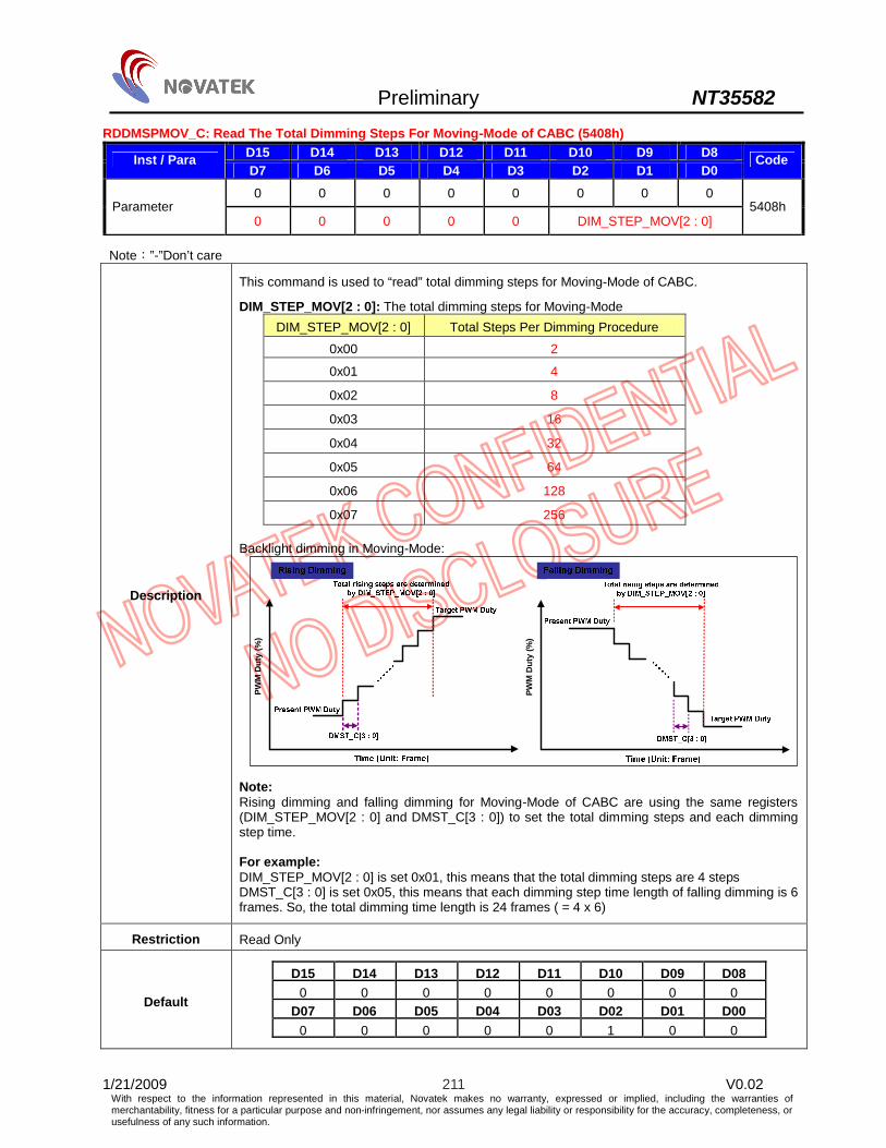
Preliminary NT35582
1/21/2009 211 V0.02 With respect to the information represented in this material, Novatek makes no warranty, expressed or implied, including the warranties of merchantability, fitness for a particular purpose and non-infringement, nor assumes any legal liability or responsibility for the accuracy, completeness, or usefulness of any such information.
RDDMSPMOV_C: Read The Total Dimming Steps For Moving-Mode of CABC (5408h) D15 D14 D13 D12 D11 D10 D9 D8 Inst / Para D7 D6 D5 D4 D3 D2 D1 D0
Code
0 0 0 0 0 0 0 0 Parameter
0 0 0 0 0 DIM_STEP_MOV[2 : 0] 5408h
Note:”-”Don’t care
Description
This command is used to “read” total dimming steps for Moving-Mode of CABC. DIM_STEP_MOV[2 : 0]: The total dimming steps for Moving-Mode
DIM_STEP_MOV[2 : 0] Total Steps Per Dimming Procedure
0x00 2
0x01 4
0x02 8
0x03 16
0x04 32
0x05 64
0x06 128
0x07 256 Backlight dimming in Moving-Mode:
PWM
Dut
y (%
)
PWM
Dut
y (%
)
Note: Rising dimming and falling dimming for Moving-Mode of CABC are using the same registers (DIM_STEP_MOV[2 : 0] and DMST_C[3 : 0]) to set the total dimming steps and each dimming step time. For example: DIM_STEP_MOV[2 : 0] is set 0x01, this means that the total dimming steps are 4 steps DMST_C[3 : 0] is set 0x05, this means that each dimming step time length of falling dimming is 6 frames. So, the total dimming time length is 24 frames ( = 4 x 6)
Restriction Read Only
Default
D15 D14 D13 D12 D11 D10 D09 D08 0 0 0 0 0 0 0 0
D07 D06 D05 D04 D03 D02 D01 D00 0 0 0 0 0 1 0 0
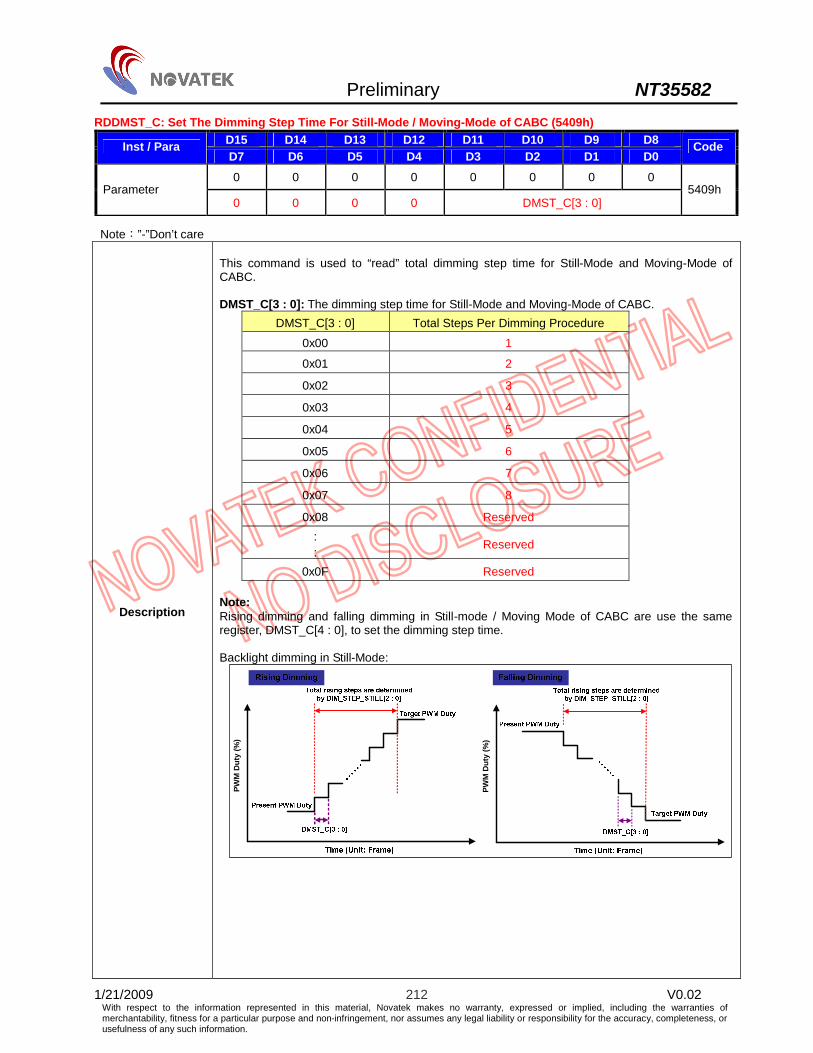
Preliminary NT35582
1/21/2009 212 V0.02 With respect to the information represented in this material, Novatek makes no warranty, expressed or implied, including the warranties of merchantability, fitness for a particular purpose and non-infringement, nor assumes any legal liability or responsibility for the accuracy, completeness, or usefulness of any such information.
RDDMST_C: Set The Dimming Step Time For Still-Mode / Moving-Mode of CABC (5409h) D15 D14 D13 D12 D11 D10 D9 D8 Inst / Para D7 D6 D5 D4 D3 D2 D1 D0
Code
0 0 0 0 0 0 0 0 Parameter
0 0 0 0 DMST_C[3 : 0] 5409h
Note:”-”Don’t care
Description
This command is used to “read” total dimming step time for Still-Mode and Moving-Mode of CABC. DMST_C[3 : 0]: The dimming step time for Still-Mode and Moving-Mode of CABC.
DMST_C[3 : 0] Total Steps Per Dimming Procedure
0x00 1
0x01 2
0x02 3
0x03 4
0x04 5
0x05 6
0x06 7
0x07 8
0x08 Reserved : :
Reserved
0x0F Reserved Note: Rising dimming and falling dimming in Still-mode / Moving Mode of CABC are use the same register, DMST_C[4 : 0], to set the dimming step time. Backlight dimming in Still-Mode:
PWM
Dut
y (%
)
PWM
Dut
y (%
)

Preliminary NT35582
1/21/2009 213 V0.02 With respect to the information represented in this material, Novatek makes no warranty, expressed or implied, including the warranties of merchantability, fitness for a particular purpose and non-infringement, nor assumes any legal liability or responsibility for the accuracy, completeness, or usefulness of any such information.
Backlight dimming in Moving-Mode:
PWM
Dut
y (%
)
PWM
Dut
y (%
)
For example 1: DIM_STEP_STILL[2 : 0] is set 0x06, this means that the total dimming steps are 128 steps DMST_C[3 : 0] is set 0x01, this means that each dimming step time length of falling dimming is 2 frames. So, the total dimming time length is 256 frames ( = 128 x 2) For example 2: DIM_STEP_MOV[2 : 0] is set 0x01, this means that the total dimming steps are 4 steps DMST_C[3 : 0] is set 0x05, this means that each dimming step time length of falling dimming is 6 frames. So, the total dimming time length is 24 frames ( = 4 x 6)
Restriction Read Only
Default
D15 D14 D13 D12 D11 D10 D09 D08 0 0 0 0 0 0 0 0
D07 D06 D05 D04 D03 D02 D01 D00 0 0 0 0 0 0 0 0

Preliminary NT35582
1/21/2009 214 V0.02 With respect to the information represented in this material, Novatek makes no warranty, expressed or implied, including the warranties of merchantability, fitness for a particular purpose and non-infringement, nor assumes any legal liability or responsibility for the accuracy, completeness, or usefulness of any such information.
WRCABC: Write Content Adaptive Brightness Control (5500h) D15 D14 D13 D12 D11 D10 D9 D8 Inst / Para D7 D6 D5 D4 D3 D2 D1 D0
Code
0 0 0 0 0 0 0 0 Parameter
0 0 0 0 0 0 CABC_COND [1]
CABC_COND [0]
5500h
Note:”-”Don’t care
Description
This command is used to set parameters for image content based adaptive brightness control functionality. There is possible to use 4 different modes for content adaptive image functionality, which are defined on the table below.
CABC_COND[1 : 0] Function 0 0 Off (default) 0 1 User Interface Image 1 0 Still Picture Image 1 1 Moving Image
Restriction -
Default
D15 D14 D13 D12 D11 D10 D09 D08 0 0 0 0 0 0 0 0
D07 D06 D05 D04 D03 D02 D01 D00 0 0 0 0 0 0 0 0
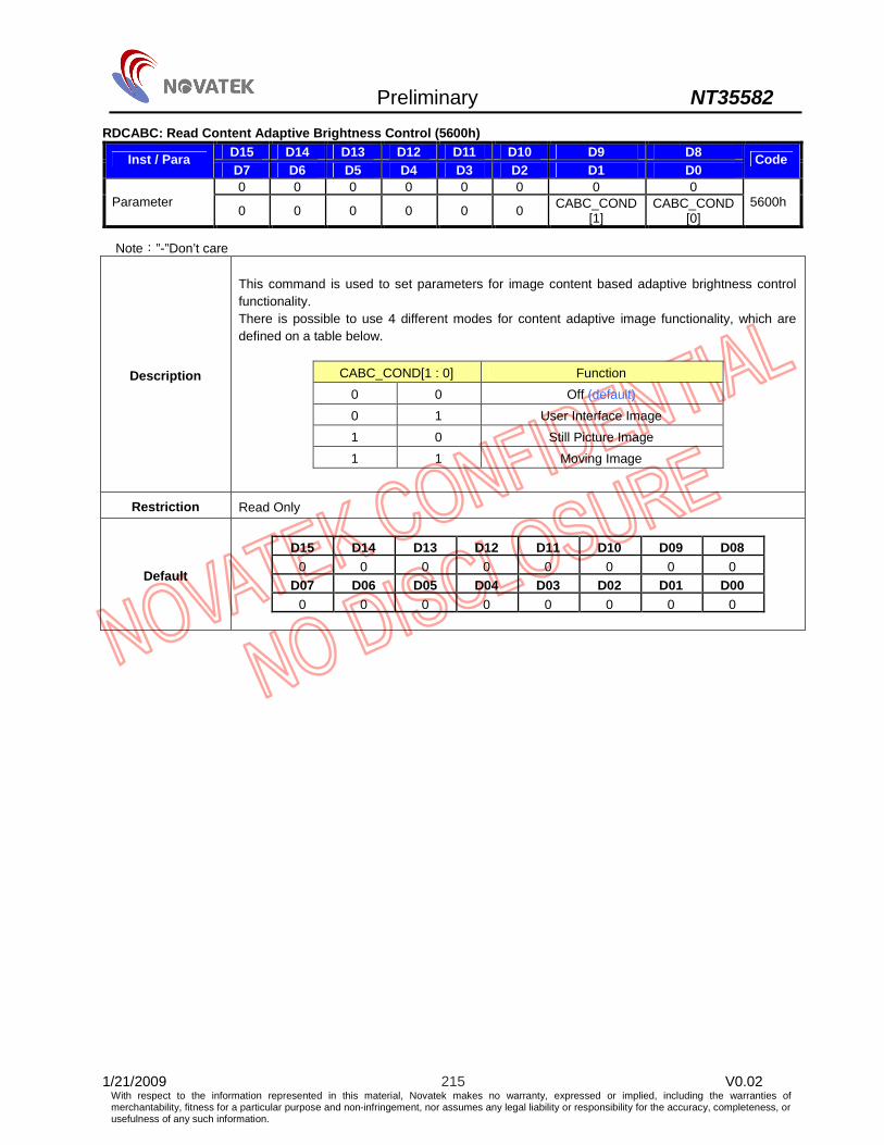
Preliminary NT35582
1/21/2009 215 V0.02 With respect to the information represented in this material, Novatek makes no warranty, expressed or implied, including the warranties of merchantability, fitness for a particular purpose and non-infringement, nor assumes any legal liability or responsibility for the accuracy, completeness, or usefulness of any such information.
RDCABC: Read Content Adaptive Brightness Control (5600h) D15 D14 D13 D12 D11 D10 D9 D8 Inst / Para D7 D6 D5 D4 D3 D2 D1 D0
Code
0 0 0 0 0 0 0 0 Parameter
0 0 0 0 0 0 CABC_COND [1]
CABC_COND [0]
5600h
Note:”-”Don’t care
Description
This command is used to set parameters for image content based adaptive brightness control functionality. There is possible to use 4 different modes for content adaptive image functionality, which are defined on a table below.
CABC_COND[1 : 0] Function 0 0 Off (default) 0 1 User Interface Image 1 0 Still Picture Image 1 1 Moving Image
Restriction Read Only
Default
D15 D14 D13 D12 D11 D10 D09 D08 0 0 0 0 0 0 0 0
D07 D06 D05 D04 D03 D02 D01 D00 0 0 0 0 0 0 0 0

Preliminary NT35582
1/21/2009 216 V0.02 With respect to the information represented in this material, Novatek makes no warranty, expressed or implied, including the warranties of merchantability, fitness for a particular purpose and non-infringement, nor assumes any legal liability or responsibility for the accuracy, completeness, or usefulness of any such information.
WRHYSTE: Write Increment/ Decrement Hysteresis (5700h~573Fh) D15 D14 D13 D12 D11 D10 D9 D8 Inst / Para D7 D6 D5 D4 D3 D2 D1 D0
Code
0 0 0 0 0 0 0 0 Parameter I01 [15:8] 5700h
0 0 0 0 0 0 0 0 Parameter I01 [7:0] 5701h
0 0 0 0 0 0 0 0 Parameter D01 [15:8] 5702h
0 0 0 0 0 0 0 0 Parameter D01 [7:0] 5703h
: : :
0 0 0 0 0 0 0 0 Parameter I16 [15:8]
573Ch
0 0 0 0 0 0 0 0 Parameter I16 [7:0] 573Dh
0 0 0 0 0 0 0 0 Parameter D16 [15:8] 573Eh
0 0 0 0 0 0 0 0 Parameter D16 [7:0] 573Fh
Note:”-”Don’t care
Description
This command is used to define Hysteresis filter function. I01[15 : 0] ~ I16[15 : 0] define increment values. D01[15 : 0] ~ D16[15 : 0] define decrement values. Although I01[15 : 0] ~ I16[15 : 0] and D01[15 : 0] ~ D16[15 : 0] are all 16-bit length registers, the valid value range is 0 ~ 1023 (0000h ~ 03FFh), not 0 ~ 65535 (0000h ~ FFFFh). In other words, user don’t care about the parameter values after “1023 (03FFh)”. I16[15 : 0] bits is always set to 1023 (03FFh)” internally, if I15[15 : 0] bits is still valid and less than “1023 (03FFh)”
Restriction -
Default
I01[15 : 0] ~ I16[15 : 0]: D15 D14 D13 D12 D11 D10 D09 D08
0 0 0 0 0 0 1 1 D07 D06 D05 D04 D03 D02 D01 D00
1 1 1 1 1 1 1 1 D01[15 : 0] ~ D16[15 : 0]:
D15 D14 D13 D12 D11 D10 D09 D08 0 0 0 0 0 0 1 1
D07 D06 D05 D04 D03 D02 D01 D00 1 1 1 1 1 1 1 1

Preliminary NT35582
1/21/2009 217 V0.02 With respect to the information represented in this material, Novatek makes no warranty, expressed or implied, including the warranties of merchantability, fitness for a particular purpose and non-infringement, nor assumes any legal liability or responsibility for the accuracy, completeness, or usefulness of any such information.
RDFSVM : Read MSBs of FSV Value (5A00h) D15 D14 D13 D12 D11 D10 D9 D8 Inst /
Para D7 D6 D5 D4 D3 D2 D1 D0 Code
0 Parameter FSV [15 : 8]
5A00h
Note:”-”Don’t care
Description
This command returns MSBs of the “Front Side Ambient Light Sensor Value” after the flicker has been removed from ambient light reading. Another command for LSBs (FSV[7 : 0]). See the chapter “Read LSBs of FSV Value (5B00h)”. When using read LSBs / MSBs command, corresponding MSBs / LSBs should be locked so that they refer to the same value when LSBs / MSBs are read. After reading both values, registers for MSBs and LSBs should be released. And that if e.g. LSBs are read and there is no MSBs read command, the next LSBs read will also update MSBs. If MSBs are read at first, the next MSBs read will update LSBs. If any other commands are received between LSBs read command and MSBs read command, the registers for MSBs and LSBs should be released. If user bypassed the internal medial filter by setting register “MFR_BYS” = “0”, the read value of register FSV[15 : 0] will be equal to the value of register FFSV[15 : 0]. FSV[7 : 0] should be 00h when bit ‘A’ of the “Write CTRL Display (5300h)” command is “0”. Note: Although FSV[15 : 0] is 16-bit length register, the valid value range is 0 ~ 1023 (0000h ~ 03FFh), not 0 ~ 65535 (0000h ~ FFFFh). In other words, user don’t care about the parameter values after “1023 (03FFh)”.
Restriction Read Only
Default
D15 D14 D13 D12 D11 D10 D09 D08 0 0 0 0 0 0 0 0
D07 D06 D05 D04 D03 D02 D01 D00 0 0 0 0 0 0 0 0
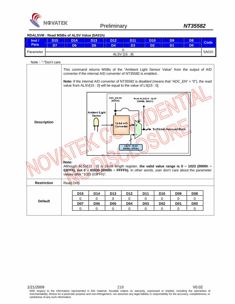
Preliminary NT35582
1/21/2009 218 V0.02 With respect to the information represented in this material, Novatek makes no warranty, expressed or implied, including the warranties of merchantability, fitness for a particular purpose and non-infringement, nor assumes any legal liability or responsibility for the accuracy, completeness, or usefulness of any such information.
RDALSVM : Read MSBs of ALSV Value (5A01h) D15 D14 D13 D12 D11 D10 D9 D8 Inst /
Para D7 D6 D5 D4 D3 D2 D1 D0 Code
0 Parameter ALSV [15 : 8]
5A01h
Note:”-”Don’t care
Description
This command returns MSBs of the “Ambient Light Sensor Value” from the output of A/D converter if the internal A/D converter of NT35582 is enabled.. Note: If the internal A/D converter of NT35582 is disabled (means that “ADC_EN” = “0”), the read value from ALSV[15 : 0] will be equal to the value of LS[15 : 0].
Note: Although ALSV[15 : 0] is 16-bit length register, the valid value range is 0 ~ 1023 (0000h ~ 03FFh), not 0 ~ 65535 (0000h ~ FFFFh). In other words, user don’t care about the parameter values after “1023 (03FFh)”.
Restriction Read Only
Default
D15 D14 D13 D12 D11 D10 D09 D08 0 0 0 0 0 0 0 0
D07 D06 D05 D04 D03 D02 D01 D00 0 0 0 0 0 0 0 0

Preliminary NT35582
1/21/2009 219 V0.02 With respect to the information represented in this material, Novatek makes no warranty, expressed or implied, including the warranties of merchantability, fitness for a particular purpose and non-infringement, nor assumes any legal liability or responsibility for the accuracy, completeness, or usefulness of any such information.
RDFSVL : Read LSBs of FS Value (5B00h) D15 D14 D13 D12 D11 D10 D9 D8 Inst /
Para D7 D6 D5 D4 D3 D2 D1 D0 Code
0 Parameter FSV [7 : 0]
5B00h
Note:”-”Don’t care
Description
This command returns LSBs of the “Front Side Ambient Light Sensor Value” after the flicker has been removed from ambient light reading. Another command for MSBs (FSV[7 : 0]). See the chapter “Read MSBs of FSV Value (5A00h)”. When using read LSBs / MSBs command, corresponding MSBs / LSBs should be locked so that they refer to the same value when LSBs / MSBs are read. After reading both values, registers for MSBs and LSBs should be released. And that if e.g. LSBs are read and there is no MSBs read command, the next LSBs read will also update MSBs. If MSBs are read at first, the next MSBs read will update LSBs. If any other commands are received between LSBs read command and MSBs read command, the registers for MSBs and LSBs should be released. If user bypassed the internal medial filter by setting register “MFR_BYS” = “0”, the read value of register FSV[15 : 0] will be equal to the value of register FFSV[15 : 0]. FSV[7 : 0] should be 00h when bit ‘A’ of “Write CTRL Display (5300h)” command is “0”. Note: Although FSV[15 : 0] is 16-bit length register, the valid value range is 0 ~ 1023 (0000h ~ 03FFh), not 0 ~ 65535 (0000h ~ FFFFh). In other words, user don’t care about the parameter values after “1023 (03FFh)”.
Restriction Read Only
Default
D15 D14 D13 D12 D11 D10 D09 D08 0 0 0 0 0 0 0 0
D07 D06 D05 D04 D03 D02 D01 D00 0 0 0 0 0 0 0 0

Preliminary NT35582
1/21/2009 220 V0.02 With respect to the information represented in this material, Novatek makes no warranty, expressed or implied, including the warranties of merchantability, fitness for a particular purpose and non-infringement, nor assumes any legal liability or responsibility for the accuracy, completeness, or usefulness of any such information.
RDALSVL : Read LSBs of ALSV Value (5B01h) D15 D14 D13 D12 D11 D10 D9 D8 Inst /
Para D7 D6 D5 D4 D3 D2 D1 D0 Code
0 Parameter ALSV [7 : 0]
5B01h
Note:”-”Don’t care
Description
This command returns LSBs of the “Ambient Light Sensor Value” from the output of A/D converter if the internal A/D converter of NT35582 is enabled.. Note: If the internal A/D converter of NT35582 is disabled (means that “ADC_EN” = “0”), the read value from ALSV[15 : 0] will be equal to the value of LS[15 : 0].
Note: Although ALSV[15 : 0] is 16-bit length register, the valid value range is 0 ~ 1023 (0000h ~ 03FFh), not 0 ~ 65535 (0000h ~ FFFFh). In other words, user don’t care about the parameter values after “1023 (03FFh)”.
Restriction Read Only
Default
D15 D14 D13 D12 D11 D10 D09 D08 0 0 0 0 0 0 0 0
D07 D06 D05 D04 D03 D02 D01 D00 0 0 0 0 0 0 0 0

Preliminary NT35582
1/21/2009 221 V0.02 With respect to the information represented in this material, Novatek makes no warranty, expressed or implied, including the warranties of merchantability, fitness for a particular purpose and non-infringement, nor assumes any legal liability or responsibility for the accuracy, completeness, or usefulness of any such information.
RDFFSVM : Read MSBs of Median Filtered FS Value (5C00h) D15 D14 D13 D12 D11 D10 D9 D8 Inst /
Para D7 D6 D5 D4 D3 D2 D1 D0 Code
0 Parameter FFSV [15 : 8]
5C00h
Note:”-”Don’t care
Description
This command returns MSBs of the “Front Side Ambient Light Sensor Value” after median filter. Another command for LSBs (FFSV[7 : 0]). See the chapter “Read LSBs of Median Filtered FS Value (5D00h)”. When using read LSBs / MSBs command, corresponding MSBs / LSBs should be locked so that they refer to the same value when LSBs / MSBs are read. After reading both values, registers for MSBs and LSBs should be released. And that if e.g. LSBs are read and there is no MSBs read command, the next LSBs read will also update MSBs. If MSBs are read at first, the next MSBs read will update LSBs. If any other commands are received between LSBs read command and MSBs read command, the registers for MSBs and LSBs should be released. If user bypassed the internal medial filter by setting register “MFR_BYS” = “0”, the read value of register FSV[15 : 0] will be equal to the value of register FFSV[15 : 0]. FFSV[7 : 0] status is related with some bits of other commands. See the chapter “Front Side Ambient Light Sensor Value [FSV and FFSV]”. Note: Although FFSV[15 : 0] is 16-bit length register, the valid value range is 0 ~ 1023 (0000h ~ 03FFh), not 0 ~ 65535 (0000h ~ FFFFh). In other words, user don’t care about the parameter values after “1023 (03FFh)”.
Restriction Read Only
Default
D15 D14 D13 D12 D11 D10 D09 D08 0 0 0 0 0 0 0 0
D07 D06 D05 D04 D03 D02 D01 D00 0 0 0 0 0 0 0 0

Preliminary NT35582
1/21/2009 222 V0.02 With respect to the information represented in this material, Novatek makes no warranty, expressed or implied, including the warranties of merchantability, fitness for a particular purpose and non-infringement, nor assumes any legal liability or responsibility for the accuracy, completeness, or usefulness of any such information.
RDFFSVL : Read LSBs of Median Filtered FS Value (5D00h) D15 D14 D13 D12 D11 D10 D9 D8 Inst /
Para D7 D6 D5 D4 D3 D2 D1 D0 Code
0 Parameter FFSV [7 : 0]
5D00h
Note:”-”Don’t care
Description
This command returns LSB of the “Front Side Ambient Light Sensor Value” after median filter. Another command for MSBs (FFSV[15 : 8]). See the chapter “Read MSBs of Median Filtered FS Value (5D00h)”. When using read LSBs / MSBs command, corresponding MSBs / LSBs should be locked so that they refer to the same value when LSBs / MSBs are read. After reading both values, registers for MSBs and LSBs should be released. And that if e.g. LSBs are read and there is no MSBs read command, the next LSBs read will also update MSBs. If MSBs are read at first, the next MSBs read will update LSBs. If any other commands are received between LSBs read command and MSBs read command, the registers for MSBs and LSBs should be released. If user bypassed the internal medial filter by setting register “MFR_BYS” = “0”, the read value of register FSV[15 : 0] will be equal to the value of register FFSV[15 : 0]. FFSV[15 : 8] status is related with some bits of other commands. See the chapter “Front Side Ambient Light Sensor Value [FSV and FFSV]”. Note: Although FFSV[15 : 0] is 16-bit length register, the valid value range is 0 ~ 1023 (0000h ~ 03FFh), not 0 ~ 65535 (0000h ~ FFFFh). In other words, user don’t care about the parameter values after “1023 (03FFh)”.
Restriction Read Only
Default
D15 D14 D13 D12 D11 D10 D09 D08 0 0 0 0 0 0 0 0
D07 D06 D05 D04 D03 D02 D01 D00 0 0 0 0 1 0 0 0

Preliminary NT35582
1/21/2009 223 V0.02 With respect to the information represented in this material, Novatek makes no warranty, expressed or implied, including the warranties of merchantability, fitness for a particular purpose and non-infringement, nor assumes any legal liability or responsibility for the accuracy, completeness, or usefulness of any such information.
WRCABCMB : Write CABC Minimum Brightness (5E00h) D15 D14 D13 D12 D11 D10 D9 D8 Inst /
Para D7 D6 D5 D4 D3 D2 D1 D0 Code
0 Parameter CMB [7 : 0]
5E00h
Note:”-”Don’t care
Description
This command is used to set the minimum brightness value of the display for CABC function. 00h value means the lowest brightness for CABC and FFh value means the highest brightness for CABC.
Restriction -
Default
D15 D14 D13 D12 D11 D10 D09 D08 0 0 0 0 0 0 0 0
D07 D06 D05 D04 D03 D02 D01 D00 0 0 0 0 0 0 0 0

Preliminary NT35582
1/21/2009 224 V0.02 With respect to the information represented in this material, Novatek makes no warranty, expressed or implied, including the warranties of merchantability, fitness for a particular purpose and non-infringement, nor assumes any legal liability or responsibility for the accuracy, completeness, or usefulness of any such information.
HYST_OUT_VAL : Set The Hysteresis Result Even The Internal Hysteresis Function Is Enabled / Disabled (5E01h) D15 D14 D13 D12 D11 D10 D9 D8 Inst / Para D7 D6 D5 D4 D3 D2 D1 D0
Code
0 0 0 0 0 0 0 0 Parameter
0 0 0 0 HYST_OUT_VAL[3 : 0] 5E01h
Note:”-”Don’t care
Description This command is used to set a specified hysteresis result even the internal hysteresis is enabled or disabled.
Restriction -
Default
D15 D14 D13 D12 D11 D10 D09 D08 0 0 0 0 0 0 0 0
D07 D06 D05 D04 D03 D02 D01 D00 0 0 0 0 0 0 0 0
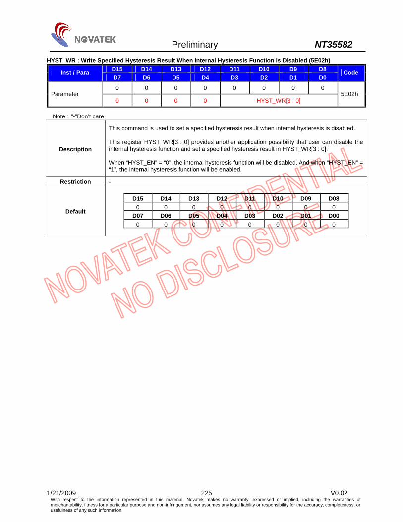
Preliminary NT35582
1/21/2009 225 V0.02 With respect to the information represented in this material, Novatek makes no warranty, expressed or implied, including the warranties of merchantability, fitness for a particular purpose and non-infringement, nor assumes any legal liability or responsibility for the accuracy, completeness, or usefulness of any such information.
HYST_WR : Write Specified Hysteresis Result When Internal Hysteresis Function Is Disabled (5E02h) D15 D14 D13 D12 D11 D10 D9 D8 Inst / Para D7 D6 D5 D4 D3 D2 D1 D0
Code
0 0 0 0 0 0 0 0 Parameter
0 0 0 0 HYST_WR[3 : 0] 5E02h
Note:”-”Don’t care
Description
This command is used to set a specified hysteresis result when internal hysteresis is disabled. This register HYST_WR[3 : 0] provides another application possibility that user can disable the internal hysteresis function and set a specified hysteresis result in HYST_WR[3 : 0]. When “HYST_EN” = “0”, the internal hysteresis function will be disabled. And when “HYST_EN” = “1”, the internal hysteresis function will be enabled.
Restriction -
Default
D15 D14 D13 D12 D11 D10 D09 D08 0 0 0 0 0 0 0 0
D07 D06 D05 D04 D03 D02 D01 D00 0 0 0 0 0 0 0 0

Preliminary NT35582
1/21/2009 226 V0.02 With respect to the information represented in this material, Novatek makes no warranty, expressed or implied, including the warranties of merchantability, fitness for a particular purpose and non-infringement, nor assumes any legal liability or responsibility for the accuracy, completeness, or usefulness of any such information.
LABC_CTRL: Control the Internal Function Block of LABC (5E03h) D15 D14 D13 D12 D11 D10 D9 D8 Inst / Para D7 D6 D5 D4 D3 D2 D1 D0
Code
0 0 0 0 0 0 0 0 Parameter
0 0 0 SR_SEL
SET_HYST
HYST_EN
MFR_BYS
ADC_EN
5E03h
Note:”-”Don’t care
Description
This command is used to set the internal function block of LABC, such as A/D Converter, Median Filter, Hysteresis Function. ADC_EN: Enable or disable the internal A/D converter
ADC_EN A/D Converter 0 Disable
1 Enable Note: When internal A/D converter is disabled (means that “ADC_EN” = “0”), the output value of A/D converter is instead of LS[15 : 0]. In other words, user can write a specified value into the register LS[15 : 0] as a ambient brightness.
Ambient Light Sensor
10-bit A/D Converter Flicker
RemovedMedian Filter Hysteresis
Read FFSV[15 : 0] bit (5C00h, 5D00h)
Read FSV[15 : 0] bit (5A00h, 5B00h)
Read ALSV[15 : 0] bit (5A01h, 5B01h)
SW1
SW2 SW3
1
0
Read RD_HYST_OUT[3 : 0] bit (5F01h)
1
0
HYST_EN bit (5E03h)
HYST_WR[3 : 0] bit (5E02h)
HYST_OUT_VAL[3 : 0] bit (5E01h)
SET_HYST bit (5E03h)MFR_BYS bit (5E03h)
Display Profiles
LABC_PWM
ADC_EN bit (5E03h)
× LSCC[15 : 0] bit
(6500h, 6501h)
220 Hz CLK
110 Hz CLK
SR_SEL bit (5E03h)Reference
Voltage(1.6V ~ 2.3V) AD_VREF[2 : 0] bit
(5E04h)
LS[15 : 0] bit(6F00h, 6F01h)
1
0
Internal LABC Block of NT35580
0
1
Internal LABC Block of Driver IC
MFR_BYS: This bit is used to decide the value of register FSV[15 : 0] to pass or bypass the median filter. As shown in above diagram, when “MFR_BYS” = “0”, the switch SW1 will be “opened”, and the switch SW2 will be “closed”, the value of register FSV[15 : 0] will pass through the median filter. Besides this, when “MFR_BYS” = “1”, the switch SW1 will be “closed”, and the switch SW2 will be “opened”, the value of register FSV[15 : 0] will bypass the median filter. Note: In here, we define:
MFR_BYS SW1 SW2 Median Filter
0 Opened Closed Pass the median filter, and median filter is enabled
1 Closed Opened Bypass the median filter, and median filter is disabled

Preliminary NT35582
1/21/2009 227 V0.02 With respect to the information represented in this material, Novatek makes no warranty, expressed or implied, including the warranties of merchantability, fitness for a particular purpose and non-infringement, nor assumes any legal liability or responsibility for the accuracy, completeness, or usefulness of any such information.
HYST_EN: This register bit is used to disabled / enabled the internal hysteresis function. As shown in above diagram, the external host (or micro processor) can read the FFSV[15 : 0], and do hysteresis by external host (or micro processor) based on the value of FFSV[15 : 0], then the external host can write it’s hysteresis result into HYST_WR[3 : 0].
HYST_EN SW3 Internal Hysteresis Function
0 Opened Disabled
1 Closed Enabled Note: In here, we still define:
SWn
Switch is opened(Not conductive!)
SWn
Switch is closed(Conductive!)
SET_HYST: This register is used to select “final” hysteresis result which comes from the internal hysteresis output (or HYST_WR[3 : 0]) or HYST_OUT_VAL[3 : 0] even the internal hysteresis function is enabled or disabled.
SET_HYST Final Hysteresis Result
0 Comes form internal hysteresis results
(or HYST_WR[3 : 0]) 1 HYST_OUT_VAL[3 : 0]
SR_SEL: Select the sample rate for internal A/D converter.
SR_SEL Sample Rate for Internal A/D Converter
0 110 Hz
1 220 Hz
Restriction Read and Write
Default
D15 D14 D13 D12 D11 D10 D09 D08
0 0 0 0 0 0 0 0 D07 D06 D05 D04 D03 D02 D01 D00
0 0 0 0 0 0 0 0

Preliminary NT35582
1/21/2009 228 V0.02 With respect to the information represented in this material, Novatek makes no warranty, expressed or implied, including the warranties of merchantability, fitness for a particular purpose and non-infringement, nor assumes any legal liability or responsibility for the accuracy, completeness, or usefulness of any such information.
AD_VREF: Select The Reference Voltage For Internal A/D Converter (5E04h) D15 D14 D13 D12 D11 D10 D9 D8 Inst / Para D7 D6 D5 D4 D3 D2 D1 D0
Code
0 0 0 0 0 0 0 0 Parameter
0 0 0 0 0 AD_VREF[2 : 0] 5E04h
Note:”-”Don’t care
Description
This command is used to set the reference voltage for internal A/D converter.
AD_VREF[2 : 0] Reference Voltage For Internal A/D Converter
0x00 1.6 V
0x01 1.7 V
0x02 1.8 V (Default)
0x03 1.9 V
0x04 2.0 V
0x05 2.1 V
0x06 2.2 V
0x07 2.3 V
Restriction Read and Write
Default
D15 D14 D13 D12 D11 D10 D09 D08
0 0 0 0 0 0 0 0 D07 D06 D05 D04 D03 D02 D01 D00
0 0 0 0 0 0 1 0

Preliminary NT35582
1/21/2009 229 V0.02 With respect to the information represented in this material, Novatek makes no warranty, expressed or implied, including the warranties of merchantability, fitness for a particular purpose and non-infringement, nor assumes any legal liability or responsibility for the accuracy, completeness, or usefulness of any such information.
RDCABCMB : Read CABC Minimum Brightness (5F00h) D15 D14 D13 D12 D11 D10 D9 D8 Inst /
Para D7 D6 D5 D4 D3 D2 D1 D0 Code
0 Parameter CMB [7 : 0]
5F00h
Note:”-”Don’t care
Description
This command us used to return the minimum brightness value of the display for CABC function. 00h value means the lowest brightness for CABC and FFh value means the highest brightness for CABC.
Restriction Read Only
Default
D15 D14 D13 D12 D11 D10 D09 D08 0 0 0 0 0 0 0 0
D07 D06 D05 D04 D03 D02 D01 D00 0 0 0 0 0 0 0 0
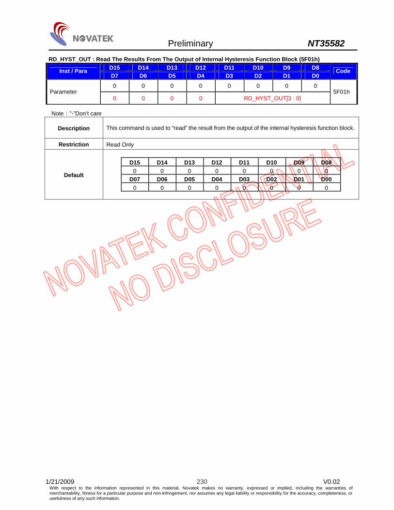
Preliminary NT35582
1/21/2009 230 V0.02 With respect to the information represented in this material, Novatek makes no warranty, expressed or implied, including the warranties of merchantability, fitness for a particular purpose and non-infringement, nor assumes any legal liability or responsibility for the accuracy, completeness, or usefulness of any such information.
RD_HYST_OUT : Read The Results From The Output of Internal Hysteresis Function Block (5F01h) D15 D14 D13 D12 D11 D10 D9 D8 Inst / Para D7 D6 D5 D4 D3 D2 D1 D0
Code
0 0 0 0 0 0 0 0 Parameter
0 0 0 0 RD_HYST_OUT[3 : 0] 5F01h
Note:”-”Don’t care
Description This command is used to “read” the result from the output of the internal hysteresis function block.
Restriction Read Only
Default
D15 D14 D13 D12 D11 D10 D09 D08 0 0 0 0 0 0 0 0
D07 D06 D05 D04 D03 D02 D01 D00 0 0 0 0 0 0 0 0

Preliminary NT35582
1/21/2009 231 V0.02 With respect to the information represented in this material, Novatek makes no warranty, expressed or implied, including the warranties of merchantability, fitness for a particular purpose and non-infringement, nor assumes any legal liability or responsibility for the accuracy, completeness, or usefulness of any such information.
WRLSCC : Write Light Sensor Compensation Coefficient Value (6500h~6501h) D15 D14 D13 D12 D11 D10 D9 D8 Inst / Para D7 D6 D5 D4 D3 D2 D1 D0
Code
0 Parameter LSCC [15 : 8]
6500h
0 Parameter LSCC [7 : 0]
6501h
Note:”-”Don’t care
Description
This command is used to send the compensation coefficient value for light sensor. Default value for compensation coefficient is 1.0 (LSCC[15 : 0] = “8000h”) Note: The LSCC[15 : 0] is 16-bit length register, so valid value range is 0000h ~ FFFFh.
Restriction -
Default
6500h: D15 D14 D13 D12 D11 D10 D09 D08
0 0 0 0 0 0 0 0 D07 D06 D05 D04 D03 D02 D01 D00
1 0 0 0 0 0 0 0 6501h:
D15 D14 D13 D12 D11 D10 D09 D08 0 0 0 0 0 0 0 0
D07 D06 D05 D04 D03 D02 D01 D00 0 0 0 0 0 0 0 0
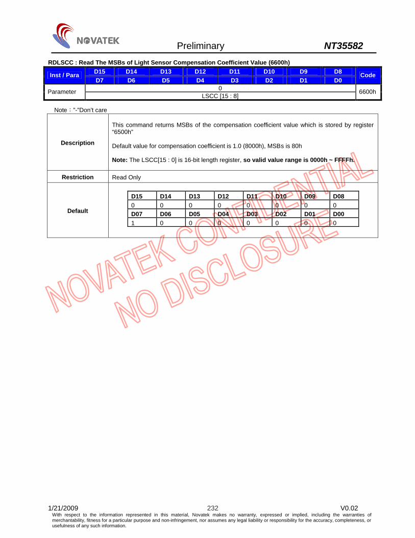
Preliminary NT35582
1/21/2009 232 V0.02 With respect to the information represented in this material, Novatek makes no warranty, expressed or implied, including the warranties of merchantability, fitness for a particular purpose and non-infringement, nor assumes any legal liability or responsibility for the accuracy, completeness, or usefulness of any such information.
RDLSCC : Read The MSBs of Light Sensor Compensation Coefficient Value (6600h) D15 D14 D13 D12 D11 D10 D9 D8 Inst / Para D7 D6 D5 D4 D3 D2 D1 D0
Code
0 Parameter LSCC [15 : 8]
6600h
Note:”-”Don’t care
Description
This command returns MSBs of the compensation coefficient value which is stored by register “6500h” Default value for compensation coefficient is 1.0 (8000h), MSBs is 80h Note: The LSCC[15 : 0] is 16-bit length register, so valid value range is 0000h ~ FFFFh.
Restriction Read Only
Default
D15 D14 D13 D12 D11 D10 D09 D08 0 0 0 0 0 0 0 0 D07 D06 D05 D04 D03 D02 D01 D00 1 0 0 0 0 0 0 0

Preliminary NT35582
1/21/2009 233 V0.02 With respect to the information represented in this material, Novatek makes no warranty, expressed or implied, including the warranties of merchantability, fitness for a particular purpose and non-infringement, nor assumes any legal liability or responsibility for the accuracy, completeness, or usefulness of any such information.
RDLSCC : Read The LSBs of Light Sensor Compensation Coefficient Value (6700h) D15 D14 D13 D12 D11 D10 D9 D8 Inst / Para D7 D6 D5 D4 D3 D2 D1 D0
Code
0 Parameter LSCC [7 : 0]
6700h
Note:”-”Don’t care
Description
This command returns LSBs of the compensation coefficient value which is stored by register “6501h” Default value for compensation coefficient is 1.0 (8000h), LSBs is 00h. Note: The LSCC[15 : 0] is 16-bit length register, so valid value range is 0000h ~ FFFFh.
Restriction Read Only
Default
D15 D14 D13 D12 D11 D10 D09 D08 0 0 0 0 0 0 0 0 D07 D06 D05 D04 D03 D02 D01 D00 0 0 0 0 0 0 0 0

Preliminary NT35582
1/21/2009 234 V0.02 With respect to the information represented in this material, Novatek makes no warranty, expressed or implied, including the warranties of merchantability, fitness for a particular purpose and non-infringement, nor assumes any legal liability or responsibility for the accuracy, completeness, or usefulness of any such information.
RDPWM: Read PWM Duty From CABC Output (6A00h) D15 D14 D13 D12 D11 D10 D9 D8 Inst /
Para D7 D6 D5 D4 D3 D2 D1 D0 Code
0 0 0 0 0 0 0 0 Parameter RDPWM[7 : 0]
6A00h
Note:”-”Don’t care RDPWM
Description
This command is used to “read” the brightness information from CABC block. The minimum brightness is 0x00, the maximum brightness is 0xFF. RDPWM[7 : 0]: The brightness status from the CABC block
RDPWM[7 : 0] PWM Duty (%) 0x00 Off 0x01 2/256
0x02 3/256
0x03 4/256
: : :
: : :
0xFE 255/256 0xFF 1 (default)
Restriction Read Only
Default
D15 D14 D13 D12 D11 D10 D09 D08 0 0 0 0 0 0 0 0
D07 D06 D05 D04 D03 D02 D01 D00 1 1 1 1 1 1 1 1
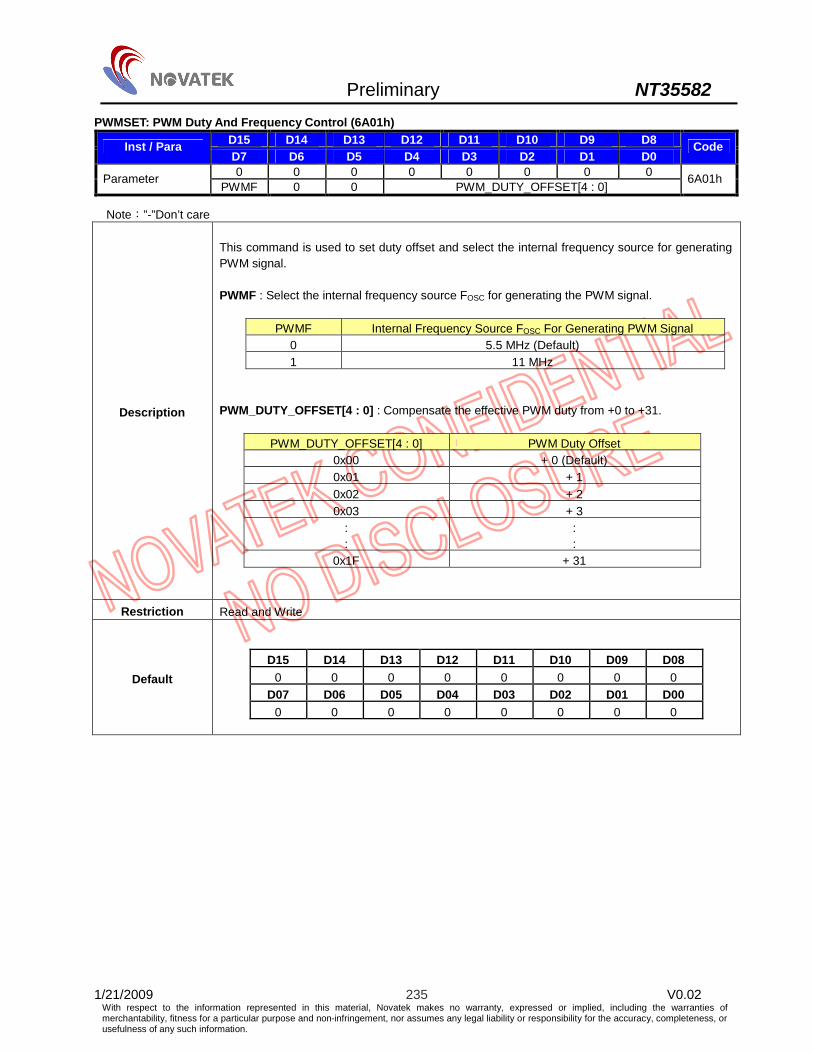
Preliminary NT35582
1/21/2009 235 V0.02 With respect to the information represented in this material, Novatek makes no warranty, expressed or implied, including the warranties of merchantability, fitness for a particular purpose and non-infringement, nor assumes any legal liability or responsibility for the accuracy, completeness, or usefulness of any such information.
PWMSET: PWM Duty And Frequency Control (6A01h) D15 D14 D13 D12 D11 D10 D9 D8 Inst / Para D7 D6 D5 D4 D3 D2 D1 D0
Code
0 0 0 0 0 0 0 0 Parameter PWMF 0 0 PWM_DUTY_OFFSET[4 : 0]
6A01h
Note:”-”Don’t care
Description
This command is used to set duty offset and select the internal frequency source for generating PWM signal. PWMF : Select the internal frequency source FOSC for generating the PWM signal.
PWMF Internal Frequency Source FOSC For Generating PWM Signal 0 5.5 MHz (Default) 1 11 MHz
PWM_DUTY_OFFSET[4 : 0] : Compensate the effective PWM duty from +0 to +31.
PWM_DUTY_OFFSET[4 : 0] PWM Duty Offset 0x00 + 0 (Default) 0x01 + 1 0x02 + 2 0x03 + 3
: :
: :
0x1F + 31
Restriction Read and Write
Default
D15 D14 D13 D12 D11 D10 D09 D08
0 0 0 0 0 0 0 0 D07 D06 D05 D04 D03 D02 D01 D00
0 0 0 0 0 0 0 0
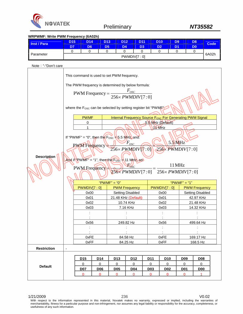
Preliminary NT35582
1/21/2009 236 V0.02 With respect to the information represented in this material, Novatek makes no warranty, expressed or implied, including the warranties of merchantability, fitness for a particular purpose and non-infringement, nor assumes any legal liability or responsibility for the accuracy, completeness, or usefulness of any such information.
WRPWMF: Write PWM Frequency (6A02h) D15 D14 D13 D12 D11 D10 D9 D8 Inst / Para D7 D6 D5 D4 D3 D2 D1 D0
Code
0 0 0 0 0 0 0 0 Parameter
PWMDIV[7 : 0] 6A02h
Note:”-”Don’t care
Description
This command is used to set PWM frequency. The PWM frequency is determined by below formula:
]0:7[256Frequency PWM
PWMDIVFOSC
where the FOSC can be selected by setting register bit “PWMF”.
PWMF Internal Frequency Source FOSC For Generating PWM Signal 0 5.5 MHz (Default) 1 11 MHz
If “PWMF” = “0”, then the FOSC = 5.5 MHz, and:
]0:7[256
MHz .55]0:7[256
Frequency PWMPWMDIVPWMDIV
FOSC
And if “PWMF” = “1”, then the FOSC = 11 MHz, so:
]0:7[256MHz 11
]0:7[256Frequency PWM
PWMDIVPWMDIVFOSC
“PWMF” = “0” “PWMF” = “1”
PWMDIV[7 : 0] PWM Frequency PWMDIV[7 : 0] PWM Frequency 0x00 Setting Disabled 0x00 Setting Disabled 0x01 21.48 KHz (Default) 0x01 42.97 KHz 0x02 10.74 KHz 0x02 21.48 KHz 0x03 7.16 KHz 0x03 14.32 KHz
: :
: :
: :
: :
0x56 249.82 Hz 0x56 499.64 Hz : :
: :
: :
: :
0xFE 84.58 Hz 0xFE 169.17 Hz 0xFF 84.25 Hz 0xFF 168.5 Hz
Restriction -
Default
D15 D14 D13 D12 D11 D10 D09 D08 0 0 0 0 0 0 0 0
D07 D06 D05 D04 D03 D02 D01 D00 0 0 0 0 0 0 0 1
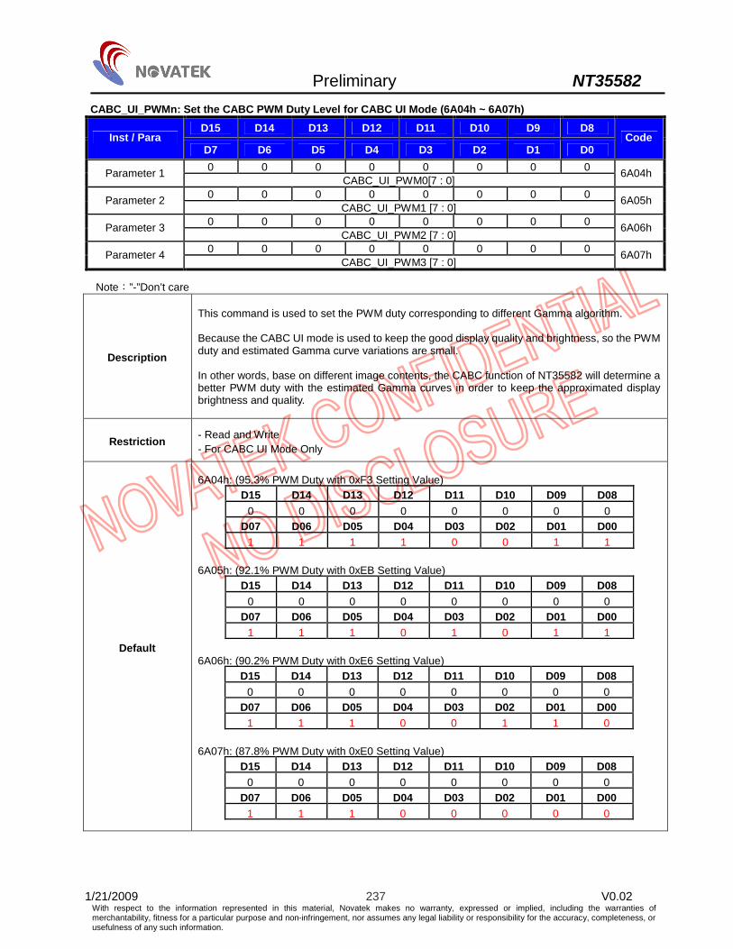
Preliminary NT35582
1/21/2009 237 V0.02 With respect to the information represented in this material, Novatek makes no warranty, expressed or implied, including the warranties of merchantability, fitness for a particular purpose and non-infringement, nor assumes any legal liability or responsibility for the accuracy, completeness, or usefulness of any such information.
CABC_UI_PWMn: Set the CABC PWM Duty Level for CABC UI Mode (6A04h ~ 6A07h)
D15 D14 D13 D12 D11 D10 D9 D8 Inst / Para
D7 D6 D5 D4 D3 D2 D1 D0 Code
0 0 0 0 0 0 0 0 Parameter 1 CABC_UI_PWM0[7 : 0]
6A04h
0 0 0 0 0 0 0 0 Parameter 2 CABC_UI_PWM1 [7 : 0]
6A05h
0 0 0 0 0 0 0 0 Parameter 3 CABC_UI_PWM2 [7 : 0]
6A06h
0 0 0 0 0 0 0 0 Parameter 4 CABC_UI_PWM3 [7 : 0]
6A07h
Note:”-”Don’t care
Description
This command is used to set the PWM duty corresponding to different Gamma algorithm. Because the CABC UI mode is used to keep the good display quality and brightness, so the PWM duty and estimated Gamma curve variations are small. In other words, base on different image contents, the CABC function of NT35582 will determine a better PWM duty with the estimated Gamma curves in order to keep the approximated display brightness and quality.
Restriction - Read and Write - For CABC UI Mode Only
Default
6A04h: (95.3% PWM Duty with 0xF3 Setting Value) D15 D14 D13 D12 D11 D10 D09 D08
0 0 0 0 0 0 0 0 D07 D06 D05 D04 D03 D02 D01 D00
1 1 1 1 0 0 1 1 6A05h: (92.1% PWM Duty with 0xEB Setting Value)
D15 D14 D13 D12 D11 D10 D09 D08 0 0 0 0 0 0 0 0
D07 D06 D05 D04 D03 D02 D01 D00 1 1 1 0 1 0 1 1
6A06h: (90.2% PWM Duty with 0xE6 Setting Value)
D15 D14 D13 D12 D11 D10 D09 D08 0 0 0 0 0 0 0 0
D07 D06 D05 D04 D03 D02 D01 D00 1 1 1 0 0 1 1 0
6A07h: (87.8% PWM Duty with 0xE0 Setting Value)
D15 D14 D13 D12 D11 D10 D09 D08 0 0 0 0 0 0 0 0
D07 D06 D05 D04 D03 D02 D01 D00 1 1 1 0 0 0 0 0

Preliminary NT35582
1/21/2009 238 V0.02 With respect to the information represented in this material, Novatek makes no warranty, expressed or implied, including the warranties of merchantability, fitness for a particular purpose and non-infringement, nor assumes any legal liability or responsibility for the accuracy, completeness, or usefulness of any such information.
RDPWM_L: Read PWM Duty From LABC Output (6A09h) D15 D14 D13 D12 D11 D10 D9 D8 Inst /
Para D7 D6 D5 D4 D3 D2 D1 D0 Code
0 0 0 0 0 0 0 0 Parameter RDPWM_L[7 : 0]
6A09h
Note:”-”Don’t care RDPWM
Description
This command is used to “read” the brightness information from LABC block. The minimum brightness is 0x00, the maximum brightness is 0xFF. RDPWM_L[7 : 0]: The brightness status from the CABC block
RDPWM_L[7 : 0] PWM Duty (%) 0x00 Off 0x01 2/256
0x02 3/256
0x03 4/256
: : :
: : :
0xFE 255/256 0xFF 1 (default)
Restriction Read Only
Default
D15 D14 D13 D12 D11 D10 D09 D08 0 0 0 0 0 0 0 0
D07 D06 D05 D04 D03 D02 D01 D00 1 1 1 1 1 1 1 1

Preliminary NT35582
1/21/2009 239 V0.02 With respect to the information represented in this material, Novatek makes no warranty, expressed or implied, including the warranties of merchantability, fitness for a particular purpose and non-infringement, nor assumes any legal liability or responsibility for the accuracy, completeness, or usefulness of any such information.
FKP: Set the Averaging Time Period for Flicker Filter (6A12h) D15 D14 D13 D12 D11 D10 D9 D8 Inst / Para D7 D6 D5 D4 D3 D2 D1 D0
Code
0 0 0 0 0 0 0 0 Parameter
0 0 0 0 FKP[3 : 0] 6A12h
Note:”-”Don’t care
Description
Set the averaging time period for flicker filter.
FKP[3 : 0] Averaging time Period For Flicker Filter (sec.) 00h 0.2 sec 01h 0.4 sec 02h 0.6 sec 03h 0.8 sec 04h 1.0 sec 05h 1.2 sec 06h 1.4 sec 07h 1.6 sec
: :
: :
0Eh 3.0 sec 0Fh Reserved
Restriction Read and Write
Default
6A12h: D15 D14 D13 D12 D11 D10 D09 D08
0 0 0 0 0 0 0 0 D07 D06 D05 D04 D03 D02 D01 D00
0 0 0 0 0 0 0 0

Preliminary NT35582
1/21/2009 240 V0.02 With respect to the information represented in this material, Novatek makes no warranty, expressed or implied, including the warranties of merchantability, fitness for a particular purpose and non-infringement, nor assumes any legal liability or responsibility for the accuracy, completeness, or usefulness of any such information.
WRALS: Write Ambient Light Sensor Value (6A15h~6A16h) D15 D14 D13 D12 D11 D10 D9 D8 Inst /
Para D7 D6 D5 D4 D3 D2 D1 D0 Code
0 0 0 0 0 0 0 0 Parameter
ALS_W 0 0 0 0 0 LS[9 : 8] 6A15h
0 0 0 0 0 0 0 0 Parameter
LS[7 : 0] 6A16h
Note:”-”Don’t care
Description
This command is used to set the ambient light sensor value if ambient light information is send from MPU. ALS_W: When user want to write a value into LS[9 : 0], please set this bit as ‘1’. And after the NT35582 has accepted the LS[9 : 0] setting value, the ALS_W will automatically be clear as ‘0’. LS[9 : 0] : Ambient light sensor value.
Restriction Read and Write
Default
6A15h: D15 D14 D13 D12 D11 D10 D09 D08
0 0 0 0 0 0 0 0 D07 D06 D05 D04 D03 D02 D01 D00
0 0 0 0 0 0 0 0 6A16h:
D15 D14 D13 D12 D11 D10 D09 D08 0 0 0 0 0 0 0 0
D07 D06 D05 D04 D03 D02 D01 D00 0 0 0 0 0 0 0 0

Preliminary NT35582
1/21/2009 241 V0.02 With respect to the information represented in this material, Novatek makes no warranty, expressed or implied, including the warranties of merchantability, fitness for a particular purpose and non-infringement, nor assumes any legal liability or responsibility for the accuracy, completeness, or usefulness of any such information.
CABC_FORCE1: Force CABC PWM in Some Conditions (6A17h) D15 D14 D13 D12 D11 D10 D9 D8 Inst / Para D7 D6 D5 D4 D3 D2 D1 D0
Code
0 0 0 0 0 0 0 0 Parameter
0 0 0 0 0 0 0 FORCE_CABC_PWM 6A17h
Note:”-”Don’t care
Description
This command is used to force the PWM duty of “CABC block” output in some conditions. FORCE_CABC_PWM: Force the CABC PWM duty as the setting of FORCE_CABC_DUTY[7 : 0]
FORCE_CABC_PWM Force PWM Duty for CABC Block Function
0 Disable (Default)
1 Enable
When FORCE_CABC_PWM = “1”, the PWM duty of “CABC block” output will be fixed the duty as FORCE_CABC_DUTY[7 : 0] setting.
Restriction Read and Write
Default
D15 D14 D13 D12 D11 D10 D09 D08 0 0 0 0 0 0 0 0
D07 D06 D05 D04 D03 D02 D01 D00 0 0 0 0 0 0 0 0

Preliminary NT35582
1/21/2009 242 V0.02 With respect to the information represented in this material, Novatek makes no warranty, expressed or implied, including the warranties of merchantability, fitness for a particular purpose and non-infringement, nor assumes any legal liability or responsibility for the accuracy, completeness, or usefulness of any such information.
CABC_FORCE2: Force CABC PWM in Some Conditions (6A18h) D15 D14 D13 D12 D11 D10 D9 D8 Inst / Para D7 D6 D5 D4 D3 D2 D1 D0
Code
0 0 0 0 0 0 0 0 Parameter FORCE_CABC_DUTY[7 : 0]
6A18
Note:”-”Don’t care
Description
This command is used to force the CABC PWM in some conditions. FORCE_CABC_DUTY[7 : 0]: If FORCE_CABC_PWM = 1, the duty of CABC PWM is the setting of FORCE_CABC_DUTY[7 : 0].
FORCE_CABC_DUTY [7 : 0] PWM Duty
0x00 Off 0x01 2/256
0x02 3/256
0x03 4/256
: : :
: : :
0xFE 255/256 0xFF 1
Restriction Read and Write
Default
D15 D14 D13 D12 D11 D10 D09 D08
0 0 0 0 0 0 0 0 D07 D06 D05 D04 D03 D02 D01 D00
1 1 1 1 1 1 1 1
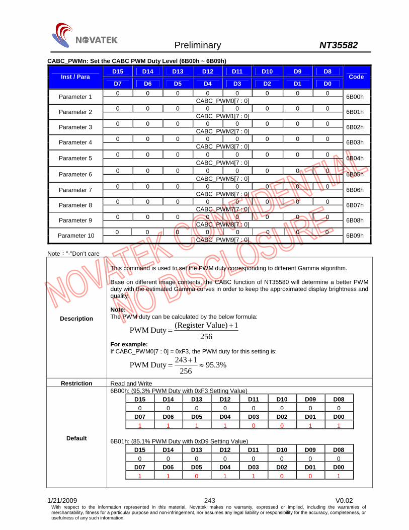
Preliminary NT35582
1/21/2009 243 V0.02 With respect to the information represented in this material, Novatek makes no warranty, expressed or implied, including the warranties of merchantability, fitness for a particular purpose and non-infringement, nor assumes any legal liability or responsibility for the accuracy, completeness, or usefulness of any such information.
CABC_PWMn: Set the CABC PWM Duty Level (6B00h ~ 6B09h)
D15 D14 D13 D12 D11 D10 D9 D8 Inst / Para
D7 D6 D5 D4 D3 D2 D1 D0 Code
0 0 0 0 0 0 0 0 Parameter 1 CABC_PWM0[7 : 0]
6B00h
0 0 0 0 0 0 0 0 Parameter 2 CABC_PWM1[7 : 0]
6B01h
0 0 0 0 0 0 0 0 Parameter 3 CABC_PWM2[7 : 0]
6B02h
0 0 0 0 0 0 0 0 Parameter 4 CABC_PWM3[7 : 0]
6B03h
0 0 0 0 0 0 0 0 Parameter 5 CABC_PWM4[7 : 0]
6B04h
0 0 0 0 0 0 0 0 Parameter 6 CABC_PWM5[7 : 0]
6B05h
0 0 0 0 0 0 0 0 Parameter 7 CABC_PWM6[7 : 0]
6B06h
0 0 0 0 0 0 0 0 Parameter 8 CABC_PWM7[7 : 0]
6B07h
0 0 0 0 0 0 0 0 Parameter 9 CABC_PWM8[7 : 0]
6B08h
0 0 0 0 0 0 0 0 Parameter 10
CABC_PWM9[7 : 0] 6B09h
Note:”-”Don’t care
Description
This command is used to set the PWM duty corresponding to different Gamma algorithm. Base on different image contents, the CABC function of NT35580 will determine a better PWM duty with the estimated Gamma curves in order to keep the approximated display brightness and quality. Note: The PWM duty can be calculated by the below formula:
2561 Value)(Register Duty PWM
For example: If CABC_PWM0[7 : 0] = 0xF3, the PWM duty for this setting is:
%3.95256
1 243 Duty PWM
Restriction Read and Write
Default
6B00h: (95.3% PWM Duty with 0xF3 Setting Value) D15 D14 D13 D12 D11 D10 D09 D08
0 0 0 0 0 0 0 0 D07 D06 D05 D04 D03 D02 D01 D00
1 1 1 1 0 0 1 1 6B01h: (85.1% PWM Duty with 0xD9 Setting Value)
D15 D14 D13 D12 D11 D10 D09 D08 0 0 0 0 0 0 0 0
D07 D06 D05 D04 D03 D02 D01 D00 1 1 0 1 1 0 0 1

Preliminary NT35582
1/21/2009 244 V0.02 With respect to the information represented in this material, Novatek makes no warranty, expressed or implied, including the warranties of merchantability, fitness for a particular purpose and non-infringement, nor assumes any legal liability or responsibility for the accuracy, completeness, or usefulness of any such information.
6B02h: (80% PWM Duty with 0xCC Setting Value) D15 D14 D13 D12 D11 D10 D09 D08
0 0 0 0 0 0 0 0 D07 D06 D05 D04 D03 D02 D01 D00
1 1 0 0 1 1 0 0 6B03h: (75.4% PWM Duty with 0xC0 Setting Value)
D15 D14 D13 D12 D11 D10 D09 D08 0 0 0 0 0 0 0 0
D07 D06 D05 D04 D03 D02 D01 D00 1 1 0 0 0 0 0 0
6B04h: (70.3% PWM Duty with 0xB3 Setting Value)
D15 D14 D13 D12 D11 D10 D09 D08 0 0 0 0 0 0 0 0
D07 D06 D05 D04 D03 D02 D01 D00 1 0 1 1 0 0 1 1
6B05h: (65.2% PWM Duty with 0xA6 Setting Value)
D15 D14 D13 D12 D11 D10 D09 D08 0 0 0 0 0 0 0 0
D07 D06 D05 D04 D03 D02 D01 D00 1 0 1 0 0 1 1 0
6B06h: (60.1% PWM Duty with 0x99 Setting Value)
D15 D14 D13 D12 D11 D10 D09 D08 0 0 0 0 0 0 0 0
D07 D06 D05 D04 D03 D02 D01 D00 1 0 0 1 1 0 0 1
6B07h: (60.1% PWM Duty with 0x99 Setting Value)
D15 D14 D13 D12 D11 D10 D09 D08 0 0 0 0 0 0 0 0
D07 D06 D05 D04 D03 D02 D01 D00 1 0 0 1 1 0 0 1
6B08h: (60.1% PWM Duty with 0x99 Setting Value)
D15 D14 D13 D12 D11 D10 D09 D08 0 0 0 0 0 0 0 0
D07 D06 D05 D04 D03 D02 D01 D00 1 0 0 1 1 0 0 1
6B09h: (60.1% PWM Duty with 0x99 Setting Value)
D15 D14 D13 D12 D11 D10 D09 D08 0 0 0 0 0 0 0 0
D07 D06 D05 D04 D03 D02 D01 D00 1 0 0 1 1 0 0 1
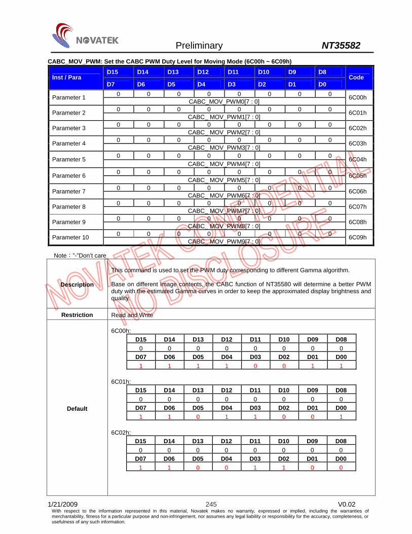
Preliminary NT35582
1/21/2009 245 V0.02 With respect to the information represented in this material, Novatek makes no warranty, expressed or implied, including the warranties of merchantability, fitness for a particular purpose and non-infringement, nor assumes any legal liability or responsibility for the accuracy, completeness, or usefulness of any such information.
CABC_MOV_PWM: Set the CABC PWM Duty Level for Moving Mode (6C00h ~ 6C09h)
D15 D14 D13 D12 D11 D10 D9 D8 Inst / Para
D7 D6 D5 D4 D3 D2 D1 D0 Code
0 0 0 0 0 0 0 0 Parameter 1 CABC_MOV_PWM0[7 : 0]
6C00h
0 0 0 0 0 0 0 0 Parameter 2 CABC_ MOV_PWM1[7 : 0]
6C01h
0 0 0 0 0 0 0 0 Parameter 3 CABC_ MOV_PWM2[7 : 0]
6C02h
0 0 0 0 0 0 0 0 Parameter 4 CABC_ MOV_PWM3[7 : 0]
6C03h
0 0 0 0 0 0 0 0 Parameter 5 CABC_ MOV_PWM4[7 : 0]
6C04h
0 0 0 0 0 0 0 0 Parameter 6 CABC_ MOV_PWM5[7 : 0]
6C05h
0 0 0 0 0 0 0 0 Parameter 7 CABC_ MOV_PWM6[7 : 0]
6C06h
0 0 0 0 0 0 0 0 Parameter 8 CABC_ MOV_PWM7[7 : 0]
6C07h
0 0 0 0 0 0 0 0 Parameter 9 CABC_ MOV_PWM8[7 : 0]
6C08h
0 0 0 0 0 0 0 0 Parameter 10 CABC_ MOV_PWM9[7 : 0]
6C09h
Note:”-”Don’t care
Description
This command is used to set the PWM duty corresponding to different Gamma algorithm. Base on different image contents, the CABC function of NT35580 will determine a better PWM duty with the estimated Gamma curves in order to keep the approximated display brightness and quality.
Restriction Read and Write
Default
6C00h:
D15 D14 D13 D12 D11 D10 D09 D08 0 0 0 0 0 0 0 0
D07 D06 D05 D04 D03 D02 D01 D00 1 1 1 1 0 0 1 1
6C01h:
D15 D14 D13 D12 D11 D10 D09 D08 0 0 0 0 0 0 0 0
D07 D06 D05 D04 D03 D02 D01 D00 1 1 0 1 1 0 0 1
6C02h:
D15 D14 D13 D12 D11 D10 D09 D08 0 0 0 0 0 0 0 0
D07 D06 D05 D04 D03 D02 D01 D00 1 1 0 0 1 1 0 0

Preliminary NT35582
1/21/2009 246 V0.02 With respect to the information represented in this material, Novatek makes no warranty, expressed or implied, including the warranties of merchantability, fitness for a particular purpose and non-infringement, nor assumes any legal liability or responsibility for the accuracy, completeness, or usefulness of any such information.
6C03h: D15 D14 D13 D12 D11 D10 D09 D08
0 0 0 0 0 0 0 0 D07 D06 D05 D04 D03 D02 D01 D00
1 1 0 0 0 0 0 0 6C04h:
D15 D14 D13 D12 D11 D10 D09 D08 0 0 0 0 0 0 0 0
D07 D06 D05 D04 D03 D02 D01 D00 1 0 1 1 0 0 1 1
6C05h:
D15 D14 D13 D12 D11 D10 D09 D08 0 0 0 0 0 0 0 0
D07 D06 D05 D04 D03 D02 D01 D00 1 0 1 0 0 1 1 0
6C06h:
D15 D14 D13 D12 D11 D10 D09 D08 0 0 0 0 0 0 0 0
D07 D06 D05 D04 D03 D02 D01 D00 1 0 0 1 1 0 0 1
6C07h:
D15 D14 D13 D12 D11 D10 D09 D08 0 0 0 0 0 0 0 0
D07 D06 D05 D04 D03 D02 D01 D00 1 0 0 1 1 0 0 1
6C08h:
D15 D14 D13 D12 D11 D10 D09 D08 0 0 0 0 0 0 0 0
D07 D06 D05 D04 D03 D02 D01 D00 1 0 0 1 1 0 0 1
6C09h:
D15 D14 D13 D12 D11 D10 D09 D08 0 0 0 0 0 0 0 0
D07 D06 D05 D04 D03 D02 D01 D00 1 0 0 1 1 0 0 1

Preliminary NT35582
1/21/2009 247 V0.02 With respect to the information represented in this material, Novatek makes no warranty, expressed or implied, including the warranties of merchantability, fitness for a particular purpose and non-infringement, nor assumes any legal liability or responsibility for the accuracy, completeness, or usefulness of any such information.
MOVDET: Set the Condition for Automatic Moving Mode Detection (6C0Dh) D15 D14 D13 D12 D11 D10 D9 D8 Inst / Para D7 D6 D5 D4 D3 D2 D1 D0
Code
0 0 0 0 0 0 0 0 Parameter
0 MOVDET[6 : 0] 6C0Dh
MOVSC: Set the Condition For Internal Counter of Automatic Moving Mode Detection Mechanism (6C0Eh) D15 D14 D13 D12 D11 D10 D9 D8 Inst / Para D7 D6 D5 D4 D3 D2 D1 D0
Code
0 0 0 0 0 0 0 0 Parameter
0 0 0 MOVSC[4 : 0] 6C0Eh
Note:”-”Don’t care
Description
This command is used to set the condition for automatic “Moving Mode Selection”. The moving mode means that the frame RAM is continuously updated for displaying. The CABC function of NT35582 provides three CABC modes – “UI-Mode”, “Still-Mode”, and “Moving Mode” (See the register 5500h for detailed). This function is “only” available in Normal Display Mode with CABC mode is set “Still Mode” (Register 5500h is set as 02h). In other words, when CABC mode has been set in “UI-Mode” or “Moving Mode”, “Moving Mode Detection” dose “not” work. MOVDET[6 : 0]: Set the frame RAM rate updated rate for moving-mode detection This setting is applied to set a period which the driver IC will monitor frame RAM updating rate each specified period. When MOVDET[6 : 0] is set as 00h, this function is turned-off.
MOVDET[6 : 0] Detection Condition 00h Moving Detection Disable (Default) 01h 2 frame 02h 3 frames 03h 4 frames 04h 5 frames 05h 6 frames
: : :
: : :
7Dh 126 frames 7Eh 127 frames 7Fh 128 frames
For example: If MOVDET[6 : 0] is set as 0Ah, this means the driver IC will check frame RAM update rate each 10-farme time period. MOVSC[4 : 0]: Set the de-bounce times of frame RAM updated each specified time There is an internal counter to calculate how many times does frame RAM has been updated each specified time period. If the frame RAM has been updated (even only been updated one time) each specified time length, the internal counter will increase 1. Otherwise, if the frame RAM has not been updated any time each specified time length, the internal will decrease 1.
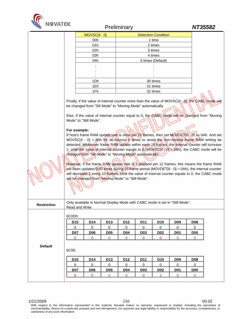
Preliminary NT35582
1/21/2009 248 V0.02 With respect to the information represented in this material, Novatek makes no warranty, expressed or implied, including the warranties of merchantability, fitness for a particular purpose and non-infringement, nor assumes any legal liability or responsibility for the accuracy, completeness, or usefulness of any such information.
MOVSC[4 : 0] Detection Condition 00h 1 time 01h 2 times 02h 3 times 03h 4 times 04h 5 times (Default)
: : :
: : :
1Dh 30 times 1Eh 31 times 1Fh 32 times
Finally, if the value of internal counter more than the value of MOVSC[4 : 0], the CABC mode will be changed from ”Sill Mode” to “Moving Mode” automatically. Else, if the value of internal counter equal to 0, the CABC mode will be changed from ”Moving Mode” to “Still Mode”. For example: If host's frame RAM update rate is once per 10 frames, then set MOVDET[6 : 0] as 0Ah. And set MOVSC[4 : 0] = 06h for de-bounce 6 times to avoid the non-moving frame RAM writing be detected. Whenever frame RAM update within each 10 frames, the internal counter will increase 1. Until the value of internal counter equals to 6 (MOVSC[4 : 0] = 06h), the CABC mode will be changed from ”Sill Mode” to “Moving Mode” automatically. However, if the frame RAM update rate is 1 stopped per 12 frames, this means the frame RAM will been updated 0.83 times during 10 frame period (MOVDET[6 : 0] = 0Ah), the internal counter will decrease 1 every 10 frames. Until the value of internal counter equals to 0, the CABC mode will be changed from ”Moving Mode” to “Still Mode”.
Restriction Only available in Normal Display Mode with CABC mode is set in “Still Mode”. Read and Write
Default
6C0Dh:
6C0E:
D15 D14 D13 D12 D11 D10 D09 D08 0 0 0 0 0 0 0 0
D07 D06 D05 D04 D03 D02 D01 D00 0 0 0 0 0 0 0 0
D15 D14 D13 D12 D11 D10 D09 D08 0 0 0 0 0 0 0 0
D07 D06 D05 D04 D03 D02 D01 D00 0 0 0 0 0 1 0 0

Preliminary NT35582
1/21/2009 249 V0.02 With respect to the information represented in this material, Novatek makes no warranty, expressed or implied, including the warranties of merchantability, fitness for a particular purpose and non-infringement, nor assumes any legal liability or responsibility for the accuracy, completeness, or usefulness of any such information.
6.2 Manufacture Command Set
Addr. Instruction D15
D14
D13
D12
D11
D10
D09
D08 D07 D06 D05 D04 D03 D02 D01 D00
(B100H) - - - - - - - - VPA[7] VPA[6] VPA[5] VPA[4] VPA[3] VPA[2] VPA[1] VPA[0]
(B101H) - - - - - - - - - - - - - - T2[9] T2[8]
(B102H) - - - - - - - - T2[7] T2[6] T2[5] T2[4] T2[3] T2[2] T2[1] T2[0]
(B103H) - - - - - - - - - - - - - T3[2] T3[1] T3[0]
(B104H) - - - - - - - - - - T4[5] T4[4] T4[3] T4[2] T4[1] T4[0]
(B105H) - - - - - - - - - - T5[5] T5[4] T5[3] T5[2] T5[1] T5[0]
(B106H) - - - - - - - - - - T5P[5] T5P[4] T5P[3] T5P[2] T5P[1] T5P[0]
(B107H) - - - - - - - - - T6[6] T6[5] T6[4] T6[3] T6[2] T6[1] T6[0]
(B108H) - - - - - - - - - T8[5] T8[5] T8[4] T8[3] T8[2] T8[1] T8[0]
(B109H)
Display Waveform Cycle setting
- - - - - - - - - - T9[5] T9[4] T9[3] T9[2] T9[1] T9[0]
(B200H) Driver set - - - - - - - - - - - - - - CNBWSEL CGM2
(B400H) INVCTR - - - - - - - - - - - - - - NL[1] NL [0]
(B500H) SD_SET0 - - - - - - - - - - - - - - PT[1] PT[0]
(B600H) - - - - - - - - - ISOPA[2] ISOPA[1] ISOPA[0] - - IO_SOPA[1]
IO_SOPA[1]
(B601H) - - - - - - - - - IGOPA[2] IGOPA[1] IGOPA[0] - - IO_GOPA[1]
IO_GOPA[0]
(B602H) - - - - - - - - - ISOPB[2] ISOPB[1] ISOPB[0] - - IO_SOPB[1]
IO_SOPB[1]
(B603H) - - - - - - - - - IGOPB[2] IGOPB[1] IGOPB[0] - - IO_GOPB[1]
IO_GOPB[0]
(B604H) - - - - - - - - - ISOPC[2] ISOPC[1] ISOPC[0] - - IO_SOPC[1]
IO_SOPC[1]
(B605H)
SD_OP_SET
- - - - - - - - - IGOPC[2] IGOPC[1] IGOPC[0] - - IO_GOPC[1]
IO_GOPC[0]
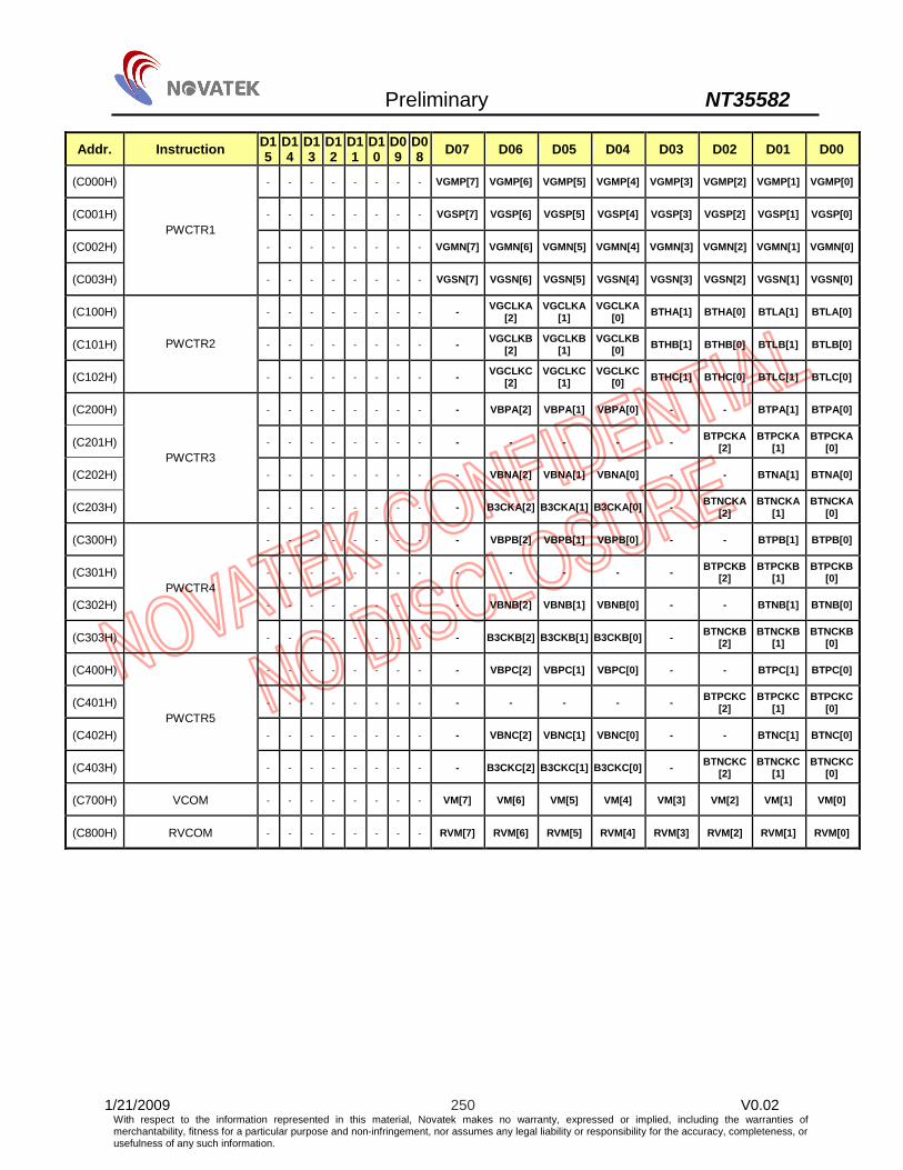
Preliminary NT35582
1/21/2009 250 V0.02 With respect to the information represented in this material, Novatek makes no warranty, expressed or implied, including the warranties of merchantability, fitness for a particular purpose and non-infringement, nor assumes any legal liability or responsibility for the accuracy, completeness, or usefulness of any such information.
Addr. Instruction D15
D14
D13
D12
D11
D10
D09
D08 D07 D06 D05 D04 D03 D02 D01 D00
(C000H) - - - - - - - - VGMP[7] VGMP[6] VGMP[5] VGMP[4] VGMP[3] VGMP[2] VGMP[1] VGMP[0]
(C001H) - - - - - - - - VGSP[7] VGSP[6] VGSP[5] VGSP[4] VGSP[3] VGSP[2] VGSP[1] VGSP[0]
(C002H) - - - - - - - - VGMN[7] VGMN[6] VGMN[5] VGMN[4] VGMN[3] VGMN[2] VGMN[1] VGMN[0]
(C003H)
PWCTR1
- - - - - - - - VGSN[7] VGSN[6] VGSN[5] VGSN[4] VGSN[3] VGSN[2] VGSN[1] VGSN[0]
(C100H) - - - - - - - - - VGCLKA [2]
VGCLKA [1]
VGCLKA [0] BTHA[1] BTHA[0] BTLA[1] BTLA[0]
(C101H) - - - - - - - - - VGCLKB [2]
VGCLKB [1]
VGCLKB [0] BTHB[1] BTHB[0] BTLB[1] BTLB[0]
(C102H)
PWCTR2
- - - - - - - - - VGCLKC [2]
VGCLKC [1]
VGCLKC [0] BTHC[1] BTHC[0] BTLC[1] BTLC[0]
(C200H) - - - - - - - - - VBPA[2] VBPA[1] VBPA[0] - - BTPA[1] BTPA[0]
(C201H) - - - - - - - - - - - - - BTPCKA [2]
BTPCKA [1]
BTPCKA [0]
(C202H) - - - - - - - - - VBNA[2] VBNA[1] VBNA[0] - - BTNA[1] BTNA[0]
(C203H)
PWCTR3
- - - - - - - - - B3CKA[2] B3CKA[1] B3CKA[0] - BTNCKA [2]
BTNCKA [1]
BTNCKA [0]
(C300H) - - - - - - - - - VBPB[2] VBPB[1] VBPB[0] - - BTPB[1] BTPB[0]
(C301H) - - - - - - - - - - - - - BTPCKB [2]
BTPCKB [1]
BTPCKB [0]
(C302H) - - - - - - - - - VBNB[2] VBNB[1] VBNB[0] - - BTNB[1] BTNB[0]
(C303H)
PWCTR4
- - - - - - - - - B3CKB[2] B3CKB[1] B3CKB[0] - BTNCKB [2]
BTNCKB [1]
BTNCKB [0]
(C400H) - - - - - - - - - VBPC[2] VBPC[1] VBPC[0] - - BTPC[1] BTPC[0]
(C401H) - - - - - - - - - - - - - BTPCKC [2]
BTPCKC [1]
BTPCKC [0]
(C402H) - - - - - - - - - VBNC[2] VBNC[1] VBNC[0] - - BTNC[1] BTNC[0]
(C403H)
PWCTR5
- - - - - - - - - B3CKC[2] B3CKC[1] B3CKC[0] - BTNCKC [2]
BTNCKC [1]
BTNCKC [0]
(C700H) VCOM - - - - - - - - VM[7] VM[6] VM[5] VM[4] VM[3] VM[2] VM[1] VM[0]
(C800H) RVCOM - - - - - - - - RVM[7] RVM[6] RVM[5] RVM[4] RVM[3] RVM[2] RVM[1] RVM[0]

Preliminary NT35582
1/21/2009 251 V0.02 With respect to the information represented in this material, Novatek makes no warranty, expressed or implied, including the warranties of merchantability, fitness for a particular purpose and non-infringement, nor assumes any legal liability or responsibility for the accuracy, completeness, or usefulness of any such information.
Addr. Instruction D15
D14
D13
D12
D11
D10
D09
D08 D07 D06 D05 D04 D03 D02 D01 D00
(E000h) - - - - - - - - - VPR0[6] VPR0[5] VPR0[4] VPR0[3] VPR0[2] VPR0[1] VPR0[0]
(E001h) - - - - - - - - - VPR1[6] VPR1[5] VPR1[4] VPR1[3] VPR1[2] VPR1[1] VPR1[0]
(E002h) - - - - - - - - VPR4[7] VPR4[6] VPR4[5] VPR4[4] VPR4[3] VPR4[2] VPR4[1] VPR4[0]
(E003h) - - - - - - - - VPR8[7] VPR8[6] VPR8[5] VPR8[4] VPR8[3] VPR8[2] VPR8[1] VPR8[0]
(E004h) - - - - - - - - - VPR16[6] VPR16[5] VPR16[4] VPR16[3] VPR16[2] VPR16[1] VPR16[0]
(E005h) - - - - - - - - - VPR24[6] VPR24[5] VPR24[4] VPR24[3] VPR24[2] VPR24[1] VPR24[0]
(E006h) - - - - - - - - - VPR52[6] VPR52[5] VPR52[4] VPR52[3] VPR52[2] VPR52[1] VPR52[0]
(E007h) - - - - - - - - VPR80[7] VPR80[6] VPR80[5] VPR80[4] VPR80[3] VPR80[2] VPR80[1] VPR80[0]
(E008h) - - - - - - - - - - VPR108 [5]
VPR108 [4]
VPR108 [3]
VPR108 [2]
VPR108 [1]
VPR108 [0]
(E009h) - - - - - - - - - - VPR147 [5]
VPR147 [4]
VPR147 [3]
VPR147 [2]
VPR147 [1]
VPR147 [0]
(E00Ah) - - - - - - - - VPR175 [7]
VPR175 [6]
VPR175 [5]
VPR175 [4]
VPR175 [3]
VPR175 [2]
VPR175 [1]
VPR175 [0]
(E00Bh) - - - - - - - - - VPR203 [6]
VPR203 [5]
VPR203 [4]
VPR203 [3]
VPR203 [2]
VPR203 [1]
VPR203 [0]
(E00Ch) - - - - - - - - - VPR231 [6]
VPR231 [5]
VPR231 [4]
VPR231 [3]
VPR231 [2]
VPR231 [1]
VPR231 [0]
(E00Dh) - - - - - - - - - VPR239 [6]
VPR239 [5]
VPR239 [4]
VPR239 [3]
VPR239 [2]
VPR239 [1]
VPR239 [0]
(E00Eh) - - - - - - - - VPR247 [7]
VPR247 [6]
VPR247 [5]
VPR247 [4]
VPR247 [3]
VPR247 [2]
VPR247 [1]
VPR247 [0]
(E00Fh) - - - - - - - - VPR251 [7]
VPR251 [6]
VPR251 [5]
VPR251 [4]
VPR251 [3]
VPR251 [2]
VPR251 [1]
VPR251 [0]
(E010h) - - - - - - - - - VPR254 [6]
VPR254 [5]
VPR254 [4]
VPR254 [3]
VPR254 [2]
VPR254 [1]
VPR254 [0]
(E011h)
GMACTRL1
- - - - - - - - - VPR255 [6]
VPR255 [5]
VPR255 [4]
VPR255 [3]
VPR255 [2]
VPR255 [1]
VPR255 [0]

Preliminary NT35582
1/21/2009 252 V0.02 With respect to the information represented in this material, Novatek makes no warranty, expressed or implied, including the warranties of merchantability, fitness for a particular purpose and non-infringement, nor assumes any legal liability or responsibility for the accuracy, completeness, or usefulness of any such information.
Addr. Instruction D15
D14
D13
D12
D11
D10
D09
D08 D07 D06 D05 D04 D03 D02 D01 D00
(E100h) - - - - - - - - - VNR0[6] VNR0[5] VNR0[4] VNR0[3] VNR0[2] VNR0[1] VNR0[0]
(E101h) - - - - - - - - - VNR1[6] VNR1[5] VNR1[4] VNR1[3] VNR1[2] VNR1[1] VNR1[0]
(E102h) - - - - - - - - VNR4[7] VNR4[6] VNR4[5] VNR4[4] VNR4[3] VNR4[2] VNR4[1] VNR4[0]
(E103h) - - - - - - - - VNR8[7] VNR8[6] VNR8[5] VNR8[4] VNR8[3] VNR8[2] VNR8[1] VNR8[0]
(E104h) - - - - - - - - - VNR16[6] VNR16[5] VNR16[4] VNR16[3] VNR16[2] VNR16[1] VNR16[0]
(E105h) - - - - - - - - - VNR24[6] VNR24[5] VNR24[4] VNR24[3] VNR24[2] VNR24[1] VNR24[0]
(E106h) - - - - - - - - - VNR52[6] VNR52[5] VNR52[4] VNR52[3] VNR52[2] VNR52[1] VNR52[0]
(E107h) - - - - - - - - VNR80[7] VNR80[6] VNR80[5] VNR80[4] VNR80[3] VNR80[2] VNR80[1] VNR80[0]
(E108h) - - - - - - - - - - VNR108 [5]
VNR108 [4]
VNR108 [3]
VNR108 [2]
VNR108 [1]
VNR108 [0]
(E109h) - - - - - - - - - - VNR147 [5]
VNR147 [4]
VNR147 [3]
VNR147 [2]
VNR147 [1]
VNR147 [0]
(E10Ah) - - - - - - - - VNR175 [7]
VNR175 [6]
VNR175 [5]
VNR175 [4]
VNR175 [3]
VNR175 [2]
VNR175 [1]
VNR175 [0]
(E10Bh) - - - - - - - - - VNR203 [6]
VNR203 [5]
VNR203 [4]
VNR203 [3]
VNR203 [2]
VNR203 [1]
VNR203 [0]
(E10Ch) - - - - - - - - - VNR231 [6]
VNR231 [5]
VNR231 [4]
VNR231 [3]
VNR231 [2]
VNR231 [1]
VNR231 [0]
(E10Dh) - - - - - - - - - VNR239 [6]
VNR239 [5]
VNR239 [4]
VNR239 [3]
VNR239 [2]
VNR239 [1]
VNR239 [0]
(E10Eh) - - - - - - - - VNR247 [7]
VNR247 [6]
VNR247 [5]
VNR247 [4]
VNR247 [3]
VNR247 [2]
VNR247 [1]
VNR247 [0]
(E10Fh) - - - - - - - - VNR251 [7]
VNR251 [6]
VNR251 [5]
VNR251 [4]
VNR251 [3]
VNR251 [2]
VNR251 [1]
VNR251 [0]
(E110h) - - - - - - - - - VNR254 [6]
VNR254 [5]
VNR254 [4]
VNR254 [3]
VNR254 [2]
VNR254 [1]
VNR254 [0]
(E111h)
GMACTRL2
- - - - - - - - - VNR255 [6]
VNR255 [5]
VNR255 [4]
VNR255 [3]
VNR255 [2]
VNR255 [1]
VNR255 [0]
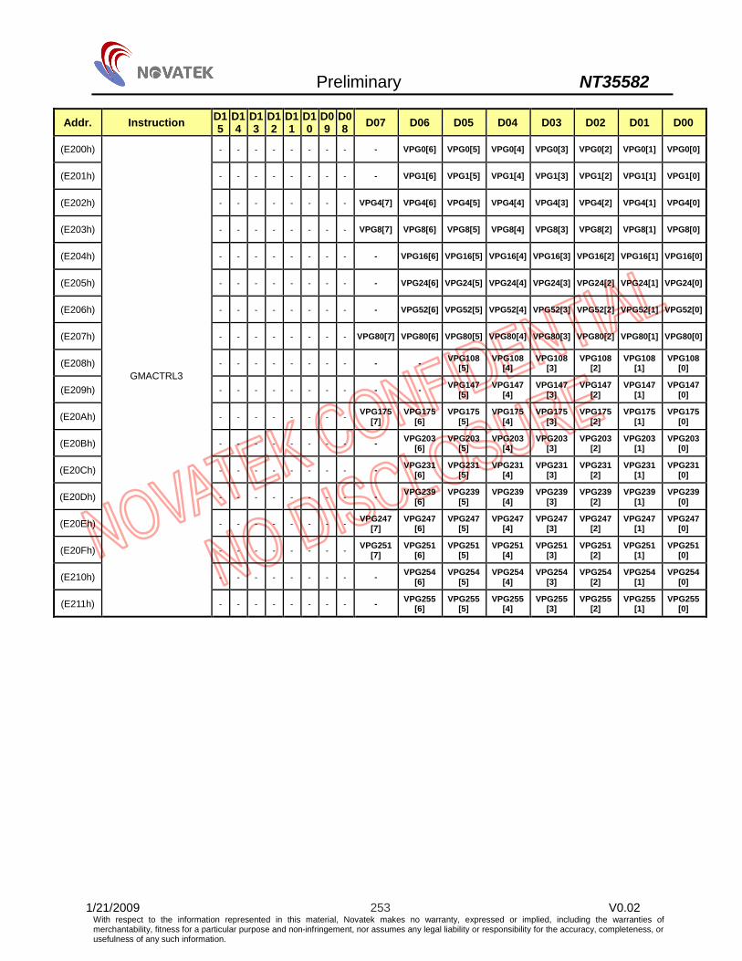
Preliminary NT35582
1/21/2009 253 V0.02 With respect to the information represented in this material, Novatek makes no warranty, expressed or implied, including the warranties of merchantability, fitness for a particular purpose and non-infringement, nor assumes any legal liability or responsibility for the accuracy, completeness, or usefulness of any such information.
Addr. Instruction D15
D14
D13
D12
D11
D10
D09
D08 D07 D06 D05 D04 D03 D02 D01 D00
(E200h) - - - - - - - - - VPG0[6] VPG0[5] VPG0[4] VPG0[3] VPG0[2] VPG0[1] VPG0[0]
(E201h) - - - - - - - - - VPG1[6] VPG1[5] VPG1[4] VPG1[3] VPG1[2] VPG1[1] VPG1[0]
(E202h) - - - - - - - - VPG4[7] VPG4[6] VPG4[5] VPG4[4] VPG4[3] VPG4[2] VPG4[1] VPG4[0]
(E203h) - - - - - - - - VPG8[7] VPG8[6] VPG8[5] VPG8[4] VPG8[3] VPG8[2] VPG8[1] VPG8[0]
(E204h) - - - - - - - - - VPG16[6] VPG16[5] VPG16[4] VPG16[3] VPG16[2] VPG16[1] VPG16[0]
(E205h) - - - - - - - - - VPG24[6] VPG24[5] VPG24[4] VPG24[3] VPG24[2] VPG24[1] VPG24[0]
(E206h) - - - - - - - - - VPG52[6] VPG52[5] VPG52[4] VPG52[3] VPG52[2] VPG52[1] VPG52[0]
(E207h) - - - - - - - - VPG80[7] VPG80[6] VPG80[5] VPG80[4] VPG80[3] VPG80[2] VPG80[1] VPG80[0]
(E208h) - - - - - - - - - - VPG108 [5]
VPG108 [4]
VPG108 [3]
VPG108 [2]
VPG108 [1]
VPG108 [0]
(E209h) - - - - - - - - - - VPG147 [5]
VPG147 [4]
VPG147 [3]
VPG147 [2]
VPG147 [1]
VPG147 [0]
(E20Ah) - - - - - - - - VPG175 [7]
VPG175 [6]
VPG175 [5]
VPG175 [4]
VPG175 [3]
VPG175 [2]
VPG175 [1]
VPG175 [0]
(E20Bh) - - - - - - - - - VPG203 [6]
VPG203 [5]
VPG203 [4]
VPG203 [3]
VPG203 [2]
VPG203 [1]
VPG203 [0]
(E20Ch) - - - - - - - - - VPG231 [6]
VPG231 [5]
VPG231 [4]
VPG231 [3]
VPG231 [2]
VPG231 [1]
VPG231 [0]
(E20Dh) - - - - - - - - - VPG239 [6]
VPG239 [5]
VPG239 [4]
VPG239 [3]
VPG239 [2]
VPG239 [1]
VPG239 [0]
(E20Eh) - - - - - - - - VPG247 [7]
VPG247 [6]
VPG247 [5]
VPG247 [4]
VPG247 [3]
VPG247 [2]
VPG247 [1]
VPG247 [0]
(E20Fh) - - - - - - - - VPG251 [7]
VPG251 [6]
VPG251 [5]
VPG251 [4]
VPG251 [3]
VPG251 [2]
VPG251 [1]
VPG251 [0]
(E210h) - - - - - - - - - VPG254 [6]
VPG254 [5]
VPG254 [4]
VPG254 [3]
VPG254 [2]
VPG254 [1]
VPG254 [0]
(E211h)
GMACTRL3
- - - - - - - - - VPG255 [6]
VPG255 [5]
VPG255 [4]
VPG255 [3]
VPG255 [2]
VPG255 [1]
VPG255 [0]

Preliminary NT35582
1/21/2009 254 V0.02 With respect to the information represented in this material, Novatek makes no warranty, expressed or implied, including the warranties of merchantability, fitness for a particular purpose and non-infringement, nor assumes any legal liability or responsibility for the accuracy, completeness, or usefulness of any such information.
Addr. Instruction D15
D14
D13
D12
D11
D10
D09
D08 D07 D06 D05 D04 D03 D02 D01 D00
(E300h) - - - - - - - - - VNG0[6] VNG0[5] VNG0[4] VNG0[3] VNG0[2] VNG0[1] VNG0[0]
(E301h) - - - - - - - - - VNG1[6] VNG1[5] VNG1[4] VNG1[3] VNG1[2] VNG1[1] VNG1[0]
(E302h) - - - - - - - - VNG4[7] VNG4[6] VNG4[5] VNG4[4] VNG4[3] VNG4[2] VNG4[1] VNG4[0]
(E303h) - - - - - - - - VNG8[7] VNG8[6] VNG8[5] VNG8[4] VNG8[3] VNG8[2] VNG8[1] VNG8[0]
(E304h) - - - - - - - - - VNG16[6] VNG16[5] VNG16[4] VNG16[3] VNG16[2] VNG16[1] VNG16[0]
(E305h) - - - - - - - - - VNG24[6] VNG24[5] VNG24[4] VNG24[3] VNG24[2] VNG24[1] VNG24[0]
(E306h) - - - - - - - - - VNG52[6] VNG52[5] VNG52[4] VNG52[3] VNG52[2] VNG52[1] VNG52[0]
(E307h) - - - - - - - - VNG80[7] VNG80[6] VNG80[5] VNG80[4] VNG80[3] VNG80[2] VNG80[1] VNG80[0]
(E308h) - - - - - - - - - - VNG108 [5]
VNG108 [4]
VNG108 [3]
VNG108 [2]
VNG108 [1]
VNG108 [0]
(E309h) - - - - - - - - - - VNG147 [5]
VNG147 [4]
VNG147 [3]
VNG147 [2]
VNG147 [1]
VNG147 [0]
(E30Ah) - - - - - - - - VNG175 [7]
VNG175 [6]
VNG175 [5]
VNG175 [4]
VNG175 [3]
VNG175 [2]
VNG175 [1]
VNG175 [0]
(E30Bh) - - - - - - - - - VNG203 [6]
VNG203 [5]
VNG203 [4]
VNG203 [3]
VNG203 [2]
VNG203 [1]
VNG203 [0]
(E30Ch) - - - - - - - - - VNG231 [6]
VNG231 [5]
VNG231 [4]
VNG231 [3]
VNG231 [2]
VNG231 [1]
VNG231 [0]
(E30Dh) - - - - - - - - - VNG239 [6]
VNG239 [5]
VNG239 [4]
VNG239 [3]
VNG239 [2]
VNG239 [1]
VNG239 [0]
(E30Eh) - - - - - - - - VNG247 [7]
VNG247 [6]
VNG247 [5]
VNG247 [4]
VNG247 [3]
VNG247 [2]
VNG247 [1]
VNG247 [0]
(E30Fh) - - - - - - - - VNG251 [7]
VNG251 [6]
VNG251 [5]
VNG251 [4]
VNG251 [3]
VNG251 [2]
VNG251 [1]
VNG251 [0]
(E310h) - - - - - - - - - VNG254 [6]
VNG254 [5]
VNG254 [4]
VNG254 [3]
VNG254 [2]
VNG254 [1]
VNG254 [0]
(E311h)
GMACTRL4
- - - - - - - - - VNG255 [6]
VNG255 [5]
VNG255 [4]
VNG255 [3]
VNG255 [2]
VNG255 [1]
VNG255 [0]

Preliminary NT35582
1/21/2009 255 V0.02 With respect to the information represented in this material, Novatek makes no warranty, expressed or implied, including the warranties of merchantability, fitness for a particular purpose and non-infringement, nor assumes any legal liability or responsibility for the accuracy, completeness, or usefulness of any such information.
Addr. Instruction D15
D14
D13
D12
D11
D10
D09
D08 D07 D06 D05 D04 D03 D02 D01 D00
(E400h) - - - - - - - - - VPB0[6] VPB0[5] VPB0[4] VPB0[3] VPB0[2] VPB0[1] VPB0[0]
(E401h) - - - - - - - - - VPB1[6] VPB1[5] VPB1[4] VPB1[3] VPB1[2] VPB1[1] VPB1[0]
(E402h) - - - - - - - - VPB4[7] VPB4[6] VPB4[5] VPB4[4] VPB4[3] VPB4[2] VPB4[1] VPB4[0]
(E403h) - - - - - - - - VPB8[7] VPB8[6] VPB8[5] VPB8[4] VPB8[3] VPB8[2] VPB8[1] VPB8[0]
(E404h) - - - - - - - - - VPB16[6] VPB16[5] VPB16[4] VPB16[3] VPB16[2] VPB16[1] VPB16[0]
(E405h) - - - - - - - - - VPB24[6] VPB24[5] VPB24[4] VPB24[3] VPB24[2] VPB24[1] VPB24[0]
(E406h) - - - - - - - - - VPB52[6] VPB52[5] VPB52[4] VPB52[3] VPB52[2] VPB52[1] VPB52[0]
(E407h) - - - - - - - - VPB80[7] VPB80[6] VPB80[5] VPB80[4] VPB80[3] VPB80[2] VPB80[1] VPB80[0]
(E408h) - - - - - - - - - - VPB108 [5]
VPB108 [4]
VPB108 [3]
VPB108 [2]
VPB108 [1]
VPB108 [0]
(E409h) - - - - - - - - - - VPB147 [5]
VPB147 [4]
VPB147 [3]
VPB147 [2]
VPB147 [1]
VPB147 [0]
(E40Ah) - - - - - - - - VPB175 [7]
VPB175 [6]
VPB175 [5]
VPB175 [4]
VPB175 [3]
VPB175 [2]
VPB175 [1]
VPB175 [0]
(E40Bh) - - - - - - - - - VPB203 [6]
VPB203 [5]
VPB203 [4]
VPB203 [3]
VPB203 [2]
VPB203 [1]
VPB203 [0]
(E40Ch) - - - - - - - - - VPB231 [6]
VPB231 [5]
VPB231 [4]
VPB231 [3]
VPB231 [2]
VPB231 [1]
VPB231 [0]
(E40Dh) - - - - - - - - - VPB239 [6]
VPB239 [5]
VPB239 [4]
VPB239 [3]
VPB239 [2]
VPB239 [1]
VPB239 [0]
(E40Eh) - - - - - - - - VPB247 [7]
VPB247 [6]
VPB247 [5]
VPB247 [4]
VPB247 [3]
VPB247 [2]
VPB247 [1]
VPB247 [0]
(E40Fh) - - - - - - - - VPB251 [7]
VPB251 [6]
VPB251 [5]
VPB251 [4]
VPB251 [3]
VPB251 [2]
VPB251 [1]
VPB251 [0]
(E410h) - - - - - - - - - VPB254 [6]
VPB254 [5]
VPB254 [4]
VPB254 [3]
VPB254 [2]
VPB254 [1]
VPB254 [0]
(E411h)
GMACTRL5
- - - - - - - - - VPB255 [6]
VPB255 [5]
VPB255 [4]
VPB255 [3]
VPB255 [2]
VPB255 [1]
VPB255 [0]

Preliminary NT35582
1/21/2009 256 V0.02 With respect to the information represented in this material, Novatek makes no warranty, expressed or implied, including the warranties of merchantability, fitness for a particular purpose and non-infringement, nor assumes any legal liability or responsibility for the accuracy, completeness, or usefulness of any such information.
Addr. Instruction D15
D14
D13
D12
D11
D10
D09
D08 D07 D06 D05 D04 D03 D02 D01 D00
(E500h) - - - - - - - - - VNB0[6] VNB0[5] VNB0[4] VNB0[3] VNB0[2] VNB0[1] VNB0[0]
(E501h) - - - - - - - - - VNB1[6] VNB1[5] VNB1[4] VNB1[3] VNB1[2] VNB1[1] VNB1[0]
(E502h) - - - - - - - - VNB4[7] VNB4[6] VNB4[5] VNB4[4] VNB4[3] VNB4[2] VNB4[1] VNB4[0]
(E503h) - - - - - - - - VNB8[7] VNB8[6] VNB8[5] VNB8[4] VNB8[3] VNB8[2] VNB8[1] VNB8[0]
(E504h) - - - - - - - - - VNB16[6] VNB16[5] VNB16[4] VNB16[3] VNB16[2] VNB16[1] VNB16[0]
(E505h) - - - - - - - - - VNB24[6] VNB24[5] VNB24[4] VNB24[3] VNB24[2] VNB24[1] VNB24[0]
(E506h) - - - - - - - - - VNB52[6] VNB52[5] VNB52[4] VNB52[3] VNB52[2] VNB52[1] VNB52[0]
(E507h) - - - - - - - - VNB80[7] VNB80[6] VNB80[5] VNB80[4] VNB80[3] VNB80[2] VNB80[1] VNB80[0]
(E508h) - - - - - - - - - - VNB108 [5]
VNB108 [4]
VNB108 [3]
VNB108 [2]
VNB108 [1]
VNB108 [0]
(E509h) - - - - - - - - - - VNB147 [5]
VNB147 [4]
VNB147 [3]
VNB147 [2]
VNB147 [1]
VNB147 [0]
(E50Ah) - - - - - - - - VNB175 [7]
VNB175 [6]
VNB175 [5]
VNB175 [4]
VNB175 [3]
VNB175 [2]
VNB175 [1]
VNB175 [0]
(E50Bh) - - - - - - - - - VNB203 [6]
VNB203 [5]
VNB203 [4]
VNB203 [3]
VNB203 [2]
VNB203 [1]
VNB203 [0]
(E50Ch) - - - - - - - - - VNB231 [6]
VNB231 [5]
VNB231 [4]
VNB231 [3]
VNB231 [2]
VNB231 [1]
VNB231 [0]
(E50Dh) - - - - - - - - - VNB239 [6]
VNB239 [5]
VNB239 [4]
VNB239 [3]
VNB239 [2]
VNB239 [1]
VNB239 [0]
(E50Eh) - - - - - - - - VNB247 [7]
VNB247 [6]
VNB247 [5]
VNB247 [4]
VNB247 [3]
VNB247 [2]
VNB247 [1]
VNB247 [0]
(E50Fh) - - - - - - - - VNB251 [7]
VNB251 [6]
VNB251 [5]
VNB251 [4]
VNB251 [3]
VNB251 [2]
VNB251 [1]
VNB251 [0]
(E510h) - - - - - - - - - VNB254 [6]
VNB254 [5]
VNB254 [4]
VNB254 [3]
VNB254 [2]
VNB254 [1]
VNB254 [0]
(E511h)
GMACTRL6
- - - - - - - - - VNB255 [6]
VNB255 [5]
VNB255 [4]
VNB255 [3]
VNB255 [2]
VNB255 [1]
VNB255 [0]

Preliminary NT35582
1/21/2009 257 V0.02 With respect to the information represented in this material, Novatek makes no warranty, expressed or implied, including the warranties of merchantability, fitness for a particular purpose and non-infringement, nor assumes any legal liability or responsibility for the accuracy, completeness, or usefulness of any such information.
Addr. Instruction D15
D14
D13
D12
D11
D10
D09
D08 D07 D06 D05 D04 D03 D02 D01 D00
(1080h) - - - - - - - - 0 1 0 1 0 1 0 1
(1180h) RDDID
- - - - - - - - 1 0 0 0 0 0 1 0
(1280h) USERID - - - - - - - - - ID [6] ID [5] ID [4] ID [3] ID [2] ID [1] ID [0]
(1380h) REVISIONID - - - - - - - - - - - - VER[3] VER[2] VER[1] VER[0]
(1C80h) RDVNT - - - - - - - - MTP_N [3]
MTP_N [2]
MTP_N [1]
MTP_N [0] - - INIT_OTP
[1] INIT_OTP
[0]
(1D80h) - - - - - - - - 0 1 0 1 0 1 0 1
(1E80h) - - - - - - - - 1 0 1 0 1 0 1 0
(1F80h)
EPWRITE
- - - - - - - - 0 1 1 0 0 1 1 0

Preliminary NT35582
1/21/2009 258 V0.02 With respect to the information represented in this material, Novatek makes no warranty, expressed or implied, including the warranties of merchantability, fitness for a particular purpose and non-infringement, nor assumes any legal liability or responsibility for the accuracy, completeness, or usefulness of any such information.
Display Waveform Cycle setting in normal mode (B100h~B109h) D15 D14 D13 D12 D11 D10 D9 D8 Inst / Para D7 D6 D5 D4 D3 D2 D1 D0
Code
0 0 0 0 0 0 0 0 VPA/Parameter VPA[7] VPA[6] VPA[5] VPA[4] VPA[3] VPA[2] VPA[1] VPA[0]
B100H
0 0 0 0 0 0 0 0 T2/Parameter 0 0 0 0 0 0 T2[9] T2[8]
B101H
0 0 0 0 0 0 0 0 T2/Parameter T2[7] T2[6] T2[5] T2[4] T2[3] T2[2] T2[1] T2[0]
B102H
0 0 0 0 0 0 0 0 T3/Parameter 0 0 0 0 0 T3[2] T3[1] T3[0]
B103H
0 0 0 0 0 0 0 0 T4/Parameter 0 0 T4[5] T4[4] T4[3] T4[2] T4[1] T4[0]
B104H
0 0 0 0 0 0 0 0 T5/Parameter 0 0 T5[5] T5[4] T5[3] T5[2] T5[1] T5[0]
B105H
0 0 0 0 0 0 0 0 T5P/Parameter 0 0 T5P[5] T5P[4] T5P[3] T5P[2] T5P[1] T5P[0]
B106H
0 0 0 0 0 0 0 0 T6/Parameter 0 T6[6] T6[5] T6[4] T6[3] T6[2] T6[1] T6[0]
B107H
0 0 0 0 0 0 0 0 T8/Parameter 0 T8[6] T8[5] T8[4] T8[3] T8[2] T8[1] T8[0]
B108H
0 0 0 0 0 0 0 0 T9/Parameter 0 0 T9[5] T9[4] T9[3] T9[2] T9[1] T9[0]
B109H
Note:”-”Don’t care
Description
.VPA[7:0]: V-sync porch for internal clocks when normal mode.
Resolution 480x864 / 480x800 / 480x640
OSC 16.5MHz
Frame Rate (T2 x ( Line+VPA[7:0])
1
Note: T1=T2=T4+2x(T5+T5P)+3x(T6)+T7+T8+T9 which is defined as below

Preliminary NT35582
1/21/2009 259 V0.02 With respect to the information represented in this material, Novatek makes no warranty, expressed or implied, including the warranties of merchantability, fitness for a particular purpose and non-infringement, nor assumes any legal liability or responsibility for the accuracy, completeness, or usefulness of any such information.
The timing definition of T2 setting to 1~1024 PCLK Delay time
T2[9:0] No. of PCLK 1/16.5MHz
0d 1 60.61ns 1d 2 121.21ns … … …
340d (Default) 341 20666.67ns … … …
1023d 1024 62060.61 ns The timing definition of T3 setting to 134~206 PCLK
Delay time T3[3:0] No. of PCLK
1/16.5MHz 0d 134 8121.21ns 1d 150 9091.5ns 2d 158 9576.38ns
3d (Default) 166 10061.26ns 4d 174 10545.45ns 5d 182 11030.30ns 6d 198 12000.00ns 7d 206 12484.85ns
The timing definition of T4 setting to 1~64 PCLK
Delay time T4[5:0] No. of PCLK 1/16.5MHz
0d 1 60.61ns 1d 2 121.21ns … … …
32d (Default) 33 2000.13ns … … …
63d 64 3879.04 ns The timing definition of T5 setting to 1~64 PCLK
Delay time T5[5:0] No. of PCLK 1/16.5MHz
0d 1 60.61ns 1d 2 121.21ns … … …
8d (Default) 9 545.49ns … … …
63d 64 3879.04 ns The timing definition of T5P setting to 1~64 PCLK

Preliminary NT35582
1/21/2009 260 V0.02 With respect to the information represented in this material, Novatek makes no warranty, expressed or implied, including the warranties of merchantability, fitness for a particular purpose and non-infringement, nor assumes any legal liability or responsibility for the accuracy, completeness, or usefulness of any such information.
Delay time T5P[5:0] No. of PCLK 1/16.5MHz
0d 1 60.61ns 1d 2 121.21ns … … …
8d (Default) 9 545.49ns … … …
63d 64 3879.04 ns The timing definition of T6 setting to 1~129 PCLK
Delay time T6[6:0] No. of PCLK 1/16.5MHz
0d 1 60.61ns 1d 2 121.21ns … … …
74d (Default) 75 4545.45ns … … …
127d 128 7758.08 ns The timing definition of T8 setting to 0~127 PCLK
Delay time T8[6:0] No. of PCLK 1/16.5MHz
0d (Default) 0 0 1d 1 60.61ns … … …
127d 127 7697.47ns The timing definition of T9 setting to 0~63 PCLK
Delay time T9[5:0] No. of PCLK 1/16.5MHz
0d (Default) 0 0 1d 1 60.61ns … … …
63d 63 3818.43ns Restriction -
Default
Address D7 D6 D5 D4 D3 D2 D1 D0 Default (B100h) 0 0 0 0 0 1 1 0 06h (B101h) 0 0 0 0 0 0 0 1 01h (B102h) 0 1 0 1 0 1 0 0 54h (B103h) 0 0 0 0 0 0 1 1 03h (B104h) 0 0 1 0 0 0 0 0 20h (B105h) 0 0 0 0 1 0 0 0 08h (B106h) 0 0 0 0 1 0 0 0 08h (B107h) 0 1 0 0 1 0 1 0 4Ah (B108h) 0 0 0 0 0 0 0 0 00h (B109h) 0 0 0 0 0 0 0 0 00h
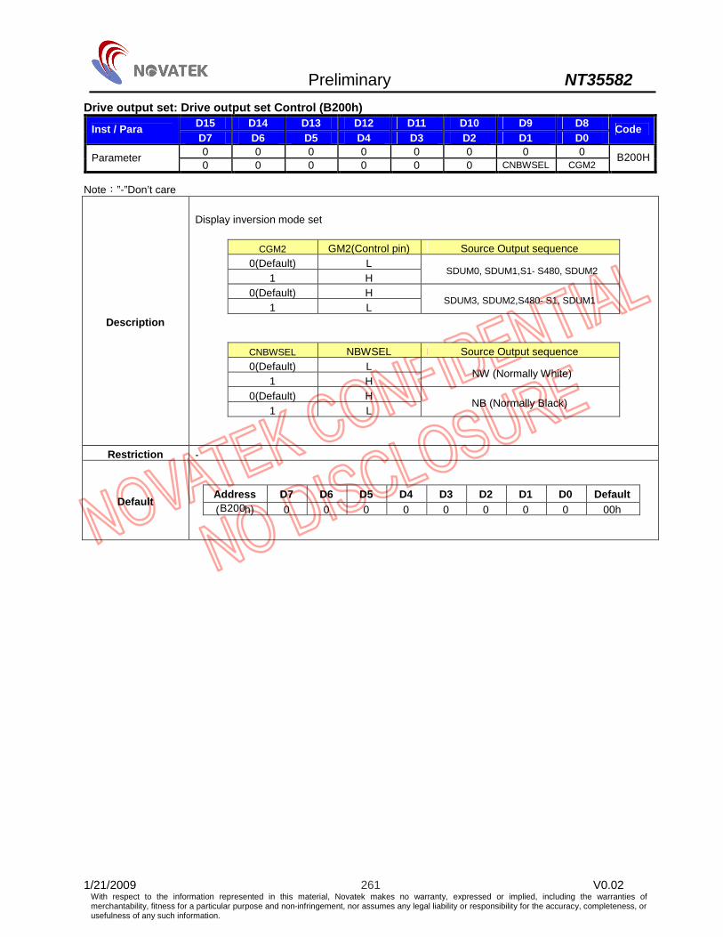
Preliminary NT35582
1/21/2009 261 V0.02 With respect to the information represented in this material, Novatek makes no warranty, expressed or implied, including the warranties of merchantability, fitness for a particular purpose and non-infringement, nor assumes any legal liability or responsibility for the accuracy, completeness, or usefulness of any such information.
Drive output set: Drive output set Control (B200h) D15 D14 D13 D12 D11 D10 D9 D8 Inst / Para D7 D6 D5 D4 D3 D2 D1 D0
Code
0 0 0 0 0 0 0 0 Parameter 0 0 0 0 0 0 CNBWSEL CGM2
B200H
Note:”-”Don’t care
Description
Display inversion mode set
CGM2 GM2(Control pin) Source Output sequence 0(Default) L
1 H SDUM0, SDUM1,S1- S480, SDUM2
0(Default) H 1 L
SDUM3, SDUM2,S480- S1, SDUM1
CNBWSEL NBWSEL Source Output sequence 0(Default) L
1 H NW (Normally White)
0(Default) H 1 L
NB (Normally Black)
Restriction -
Default Address D7 D6 D5 D4 D3 D2 D1 D0 Default (B200h) 0 0 0 0 0 0 0 0 00h
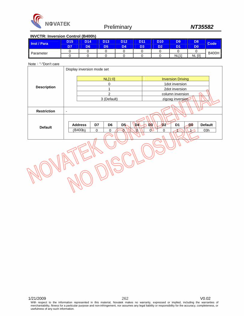
Preliminary NT35582
1/21/2009 262 V0.02 With respect to the information represented in this material, Novatek makes no warranty, expressed or implied, including the warranties of merchantability, fitness for a particular purpose and non-infringement, nor assumes any legal liability or responsibility for the accuracy, completeness, or usefulness of any such information.
INVCTR: Inversion Control (B400h) D15 D14 D13 D12 D11 D10 D9 D8 Inst / Para D7 D6 D5 D4 D3 D2 D1 D0
Code
0 0 0 0 0 0 0 0 Parameter 0 0 0 0 0 0 NL[1] NL [0]
B400H
Note:”-”Don’t care
Description
Display inversion mode set
NL[1:0] Inversion Driving 0 1dot inversion 1 2dot inversion 2 column inversion
3 (Default) zigzag inversion
Restriction -
Default Address D7 D6 D5 D4 D3 D2 D1 D0 Default (B400h) 0 0 0 0 0 0 1 1 03h

Preliminary NT35582
1/21/2009 263 V0.02 With respect to the information represented in this material, Novatek makes no warranty, expressed or implied, including the warranties of merchantability, fitness for a particular purpose and non-infringement, nor assumes any legal liability or responsibility for the accuracy, completeness, or usefulness of any such information.
SD_SET0: Source driver Control (B500h) D15 D14 D13 D12 D11 D10 D9 D8 Inst / Para D7 D6 D5 D4 D3 D2 D1 D0
Code
0 0 0 0 0 0 0 0 Parameter 0 0 0 0 0 0 PT[1] PT[0]
B500H
Note:”-”Don’t care
Description
Display set
PT[1:0] 00 V255 / V255 01 V0 / V0
10 (Default) AGND / AGND 11 Hi-Z / Hi-Z
Restriction -
Default Address D7 D6 D5 D4 D3 D2 D1 D0 Default (B500h) 0 0 0 0 0 0 1 0 02h

Preliminary NT35582
1/21/2009 264 V0.02 With respect to the information represented in this material, Novatek makes no warranty, expressed or implied, including the warranties of merchantability, fitness for a particular purpose and non-infringement, nor assumes any legal liability or responsibility for the accuracy, completeness, or usefulness of any such information.
SD_OP_SET: Source driver Control (B600h~B605h) D15 D14 D13 D12 D11 D10 D9 D8 Inst / Para D7 D6 D5 D4 D3 D2 D1 D0
Code
- - - - - - - - Parameter - ISOPA[2] ISOPA[1] ISOPA[0] - - IO_SOPA[1] IO_SOPA[1]
B600H - - - - - - - - Parameter - IGOPA[2] IGOPA[1] IGOPA[0] - - IO_GOPA[1] IO_GOPA[0]
B601H - - - - - - - - Parameter - ISOPB[2] ISOPB[1] ISOPB[0] - - IO_SOPB[1] IO_SOPB[1]
B602H - - - - - - - - Parameter - IGOPB[2] IGOPB[1] IGOPB[0] - - IO_GOPB[1] IO_GOPB[0]
B603H - - - - - - - - Parameter - ISOPC[2] ISOPC[1] ISOPC[0] - - IO_SOPC[1] IO_SOPC[1]
B604H - - - - - - - - Parameter - IGOPC[2] IGOPC[1] IGOPC[0] - - IO_GOPC[1] IO_GOPC[0]
B605H
Note:”-”Don’t care
Description
ISOPA[2:0]: ISOP setting in full colors normal mode (Normal mode on) IO_SOPA[1:0]: IO_SOP setting in full colors normal mode (Normal mode on) IGOPA[2:0]: IGOP setting in full colors normal mode (Normal mode on) IO_GOPA[1:0]: IO_GOP setting in full colors normal mode (Normal mode on) ISOPB[2:0]: ISOP setting in Idle mode (Idle mode on) IO_SOPB[1:0]: IO_SOP setting in Idle mode (Idle mode on) IGOPB[2:0]: IGOP setting in Idle mode (Idle mode on) IO_GOPB[1:0]: IO_GOP setting in Idle mode (Idle mode on) ISOPC[2:0]: ISOP setting in full colors partial mode (Partial mode on / Idle mode off) IO_SOPC[1:0]: IO_SOP setting in full colors partial mode (Partial mode on / Idle mode off) IGOPC[2:0]: IGOP setting in full colors partial mode (Partial mode on / Idle mode off) IO_GOPC[1:0]: IO_GOP setting in full colors partial mode (Partial mode on / Idle mode off) IO_SOP[1:0]:
IO_SOPA[1:0] IO_SOPB[1:0] IO_SOPC[1:0]
00 (Default) Minimum 01 Small 10 Large 11 Maximum
IO_GOP[1:0]: IO_GOPA[1:0] IO_GOPB[1:0] IO_GOPC[1:0]
00 (Default) Minimum 01 Small 10 Large 11 Maximum
IGOP[2:0]:
IGOPA[2:0] IGOPB[2:0] IGOPC[2:0]
000 (Default) Minimum 001 Small 010 Medium Low 011 Medium 100 Medium High 101 Large 110 Large High 111 Maximum

Preliminary NT35582
1/21/2009 265 V0.02 With respect to the information represented in this material, Novatek makes no warranty, expressed or implied, including the warranties of merchantability, fitness for a particular purpose and non-infringement, nor assumes any legal liability or responsibility for the accuracy, completeness, or usefulness of any such information.
ISOP[2:0]: ISOPA[2:0] ISOPB[2:0] ISOPC[2:0]
000(default) Minimum 001 Small 010 Medium Low 011 Medium 100 Medium High 101 Large 110 Large High 111 Maximum
Restriction -
Default
Address D7 D6 D5 D4 D3 D2 D1 D0 Default (B600h) 0 0 0 1 0 0 0 0 10h (B601h) 0 0 1 0 0 0 1 0 22h (B602h) 0 0 0 1 0 0 0 0 10h (B603h) 0 0 1 0 0 0 1 0 22h (B604h) 0 1 0 0 0 0 0 0 40h (B605h) 0 0 1 0 0 0 1 0 22h

Preliminary NT35582
1/21/2009 266 V0.02 With respect to the information represented in this material, Novatek makes no warranty, expressed or implied, including the warranties of merchantability, fitness for a particular purpose and non-infringement, nor assumes any legal liability or responsibility for the accuracy, completeness, or usefulness of any such information.
PWCTR1: Power Control 1 (C000h~C003h) D15 D14 D13 D12 D11 D10 D9 D8 Inst / Para D7 D6 D5 D4 D3 D2 D1 D0
Code
0 0 0 0 0 0 0 0 Parameter VGMP[7] VGMP[6] VGMP[5] VGMP[4] VGMP[3] VGMP[2] VGMP[1] VGMP[0]
C000H
0 0 0 0 0 0 0 0 Parameter
VGSP[7] VGSP[6] VGSP[5] VGSP[4] VGSP[3] VGSP[2] VGSP[1] VGSP[0] C001H
0 0 0 0 0 0 0 0 Parameter
VGMN[7] VGMN[6] VGMN[5] VGMN[4] VGMN[3] VGMN[2] VGMN[1] VGMN[0] C002H
0 0 0 0 0 0 0 0 Parameter
VGSN[7] VGSN[6] VGSN[5] VGSN[4] VGSN[3] VGSN[2] VGSN[1] VGSN[0] C003H
Note:”-”Don’t care
Description
Set the gamma regulator output voltage VGMP[7:0]: set the gamma VGMP regulator output voltage.
VGMP[7:0] Output voltage
00d 2.992V 01d 3.008V 02d 3.024V
: : :
: (STEP 1)
: 180d 5.872V
: : :
: (STEP 1)
: 206d 6.288V 207d
: 255d
NOT USE
VGSP[7:0]: set the gamma VGSP regulator output voltage.
VGSP[7:0] Output voltage
00d 0.0V(GND) 01d 0.208V 02d 0.224V 03d 0.240V
: : :
: (STEP 1)
: 221d 3.728V 222d
: 255d
NOT USE
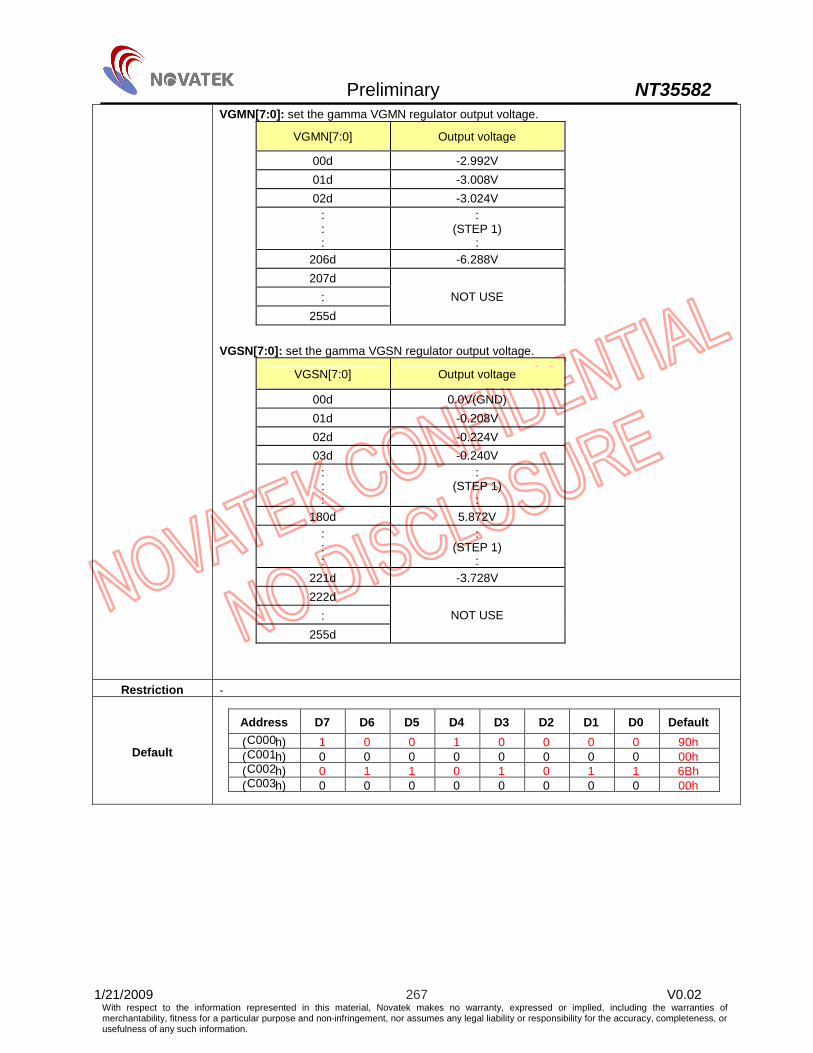
Preliminary NT35582
1/21/2009 267 V0.02 With respect to the information represented in this material, Novatek makes no warranty, expressed or implied, including the warranties of merchantability, fitness for a particular purpose and non-infringement, nor assumes any legal liability or responsibility for the accuracy, completeness, or usefulness of any such information.
VGMN[7:0]: set the gamma VGMN regulator output voltage.
VGMN[7:0] Output voltage
00d -2.992V 01d -3.008V 02d -3.024V
: : :
: (STEP 1)
: 206d -6.288V 207d
: 255d
NOT USE
VGSN[7:0]: set the gamma VGSN regulator output voltage.
VGSN[7:0] Output voltage
00d 0.0V(GND) 01d -0.208V 02d -0.224V 03d -0.240V
: : :
: (STEP 1)
: 180d 5.872V
: : :
: (STEP 1)
: 221d -3.728V 222d
: 255d
NOT USE
Restriction -
Default
Address D7 D6 D5 D4 D3 D2 D1 D0 Default (C000h) 1 0 0 1 0 0 0 0 90h (C001h) 0 0 0 0 0 0 0 0 00h (C002h) 0 1 1 0 1 0 1 1 6Bh (C003h) 0 0 0 0 0 0 0 0 00h

Preliminary NT35582
1/21/2009 268 V0.02 With respect to the information represented in this material, Novatek makes no warranty, expressed or implied, including the warranties of merchantability, fitness for a particular purpose and non-infringement, nor assumes any legal liability or responsibility for the accuracy, completeness, or usefulness of any such information.
PWCTR2: Power Control 2 (C100h~C102h) D15 D14 D13 D12 D11 D10 D9 D8 Inst / Para D7 D6 D5 D4 D3 D2 D1 D0
Code
0 0 0 0 0 0 0 0 Parameter 0 VGCLKA[2] VGCLKA[1] VGCLKA[0] BTHA[1] BTHA[0] BTLA[1] BTLA[0]
C100H
0 0 0 0 0 0 0 0 Parameter
0 VGCLKB[2] VGCLKB[1] VGCLKB[0] BTHB[1] BTHB[0] BTLB[1] BTLB[0] C101H
0 0 0 0 0 0 0 0 Parameter
0 VGCLKC[2] VGCLKC[1] VGCLKC[0] BTHC[1] BTHC[0] BTLC[1] BTLC[0] C102H
Note:”-”Don’t care
Description
Set the VGH and VGL supply power level BTHA[1:0]: VGH setting in full colors normal mode (Normal mode on) BTLA[1:0]: VGL setting in full colors normal mode (Normal mode on) VGCLKA[2:0]: VGH and VGL pump operating frequency normal mode (Normal mode on) BTHB[1:0]: VGH setting in Idle mode (Idle mode on) BTLB[1:0]: VGL setting in Idle mode (Idle mode on) VGCLKB[2:0]: VGH and VGL pump operating frequency Idle mode (Idle mode on) BTHC[1:0]: VGH setting in full colors partial mode (Partial mode on / Idle mode off) BTLC[1:0]: VGL setting in full colors partial mode (Partial mode on / Idle mode off) VGCLKC[2:0]: VGH and VGL pump operating frequency partial mode (Partial mode on / Idle mode off)
BTHA/B/C[1:0]
VGH Output voltage
00d AVDD+VCI 01d AVDD-AVEE 02d AVDD-AVEE+VCI 03d 2*AVDD-AVEE
BTLA/B/C[1:0
] VGL Output voltage
00d VCL+AVEE 01d AVEE-AVDD 02d AVEE-AVDD+VCL 03d 2*AVEE-AVDD
VGCLKA/B/C[2
:0] Frequency (DIV)
Synchronize to H sync.
00d H / 32 01d H / 16 02d H / 8 03d H / 4 04d H/2 05d H 06d 2H
Restriction -
Default
Address D7 D6 D5 D4 D3 D2 D1 D0 Default (C100h) 0 1 0 0 0 1 0 1 45h (C101h) 0 1 0 0 0 1 0 1 45h (C102h) 0 1 0 0 0 1 0 1 45h
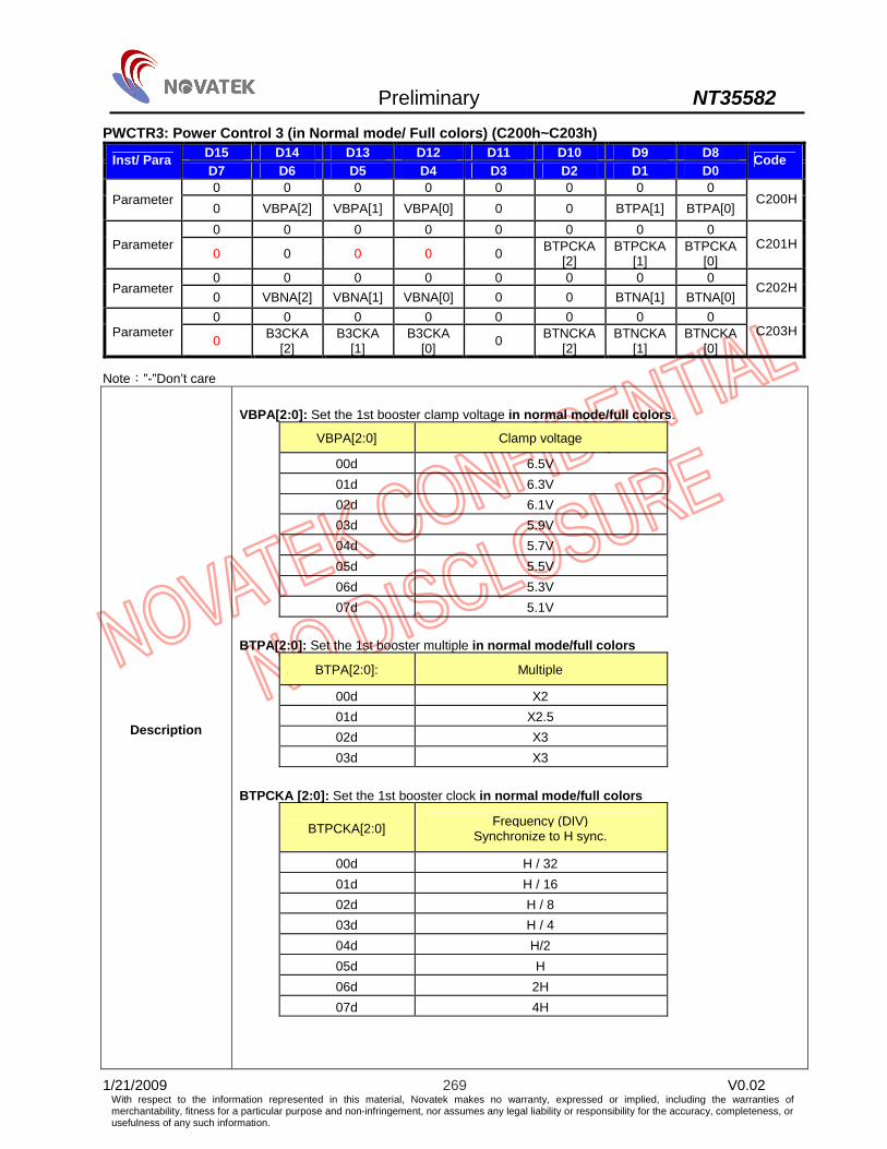
Preliminary NT35582
1/21/2009 269 V0.02 With respect to the information represented in this material, Novatek makes no warranty, expressed or implied, including the warranties of merchantability, fitness for a particular purpose and non-infringement, nor assumes any legal liability or responsibility for the accuracy, completeness, or usefulness of any such information.
PWCTR3: Power Control 3 (in Normal mode/ Full colors) (C200h~C203h) D15 D14 D13 D12 D11 D10 D9 D8 Inst/ Para D7 D6 D5 D4 D3 D2 D1 D0
Code
0 0 0 0 0 0 0 0 Parameter
0 VBPA[2] VBPA[1] VBPA[0] 0 0 BTPA[1] BTPA[0] C200H
0 0 0 0 0 0 0 0 Parameter
0 0 0 0 0 BTPCKA[2]
BTPCKA[1]
BTPCKA[0]
C201H
0 0 0 0 0 0 0 0 Parameter
0 VBNA[2] VBNA[1] VBNA[0] 0 0 BTNA[1] BTNA[0] C202H
0 0 0 0 0 0 0 0 Parameter
0 B3CKA [2]
B3CKA [1]
B3CKA [0] 0 BTNCKA
[2] BTNCKA
[1] BTNCKA
[0] C203H
Note:”-”Don’t care
Description
VBPA[2:0]: Set the 1st booster clamp voltage in normal mode/full colors.
VBPA[2:0] Clamp voltage
00d 6.5V 01d 6.3V 02d 6.1V 03d 5.9V 04d 5.7V 05d 5.5V 06d 5.3V 07d 5.1V
BTPA[2:0]: Set the 1st booster multiple in normal mode/full colors
BTPA[2:0]: Multiple
00d X2 01d X2.5 02d X3 03d X3
BTPCKA [2:0]: Set the 1st booster clock in normal mode/full colors
BTPCKA[2:0] Frequency (DIV) Synchronize to H sync.
00d H / 32 01d H / 16 02d H / 8 03d H / 4 04d H/2 05d H 06d 2H 07d 4H

Preliminary NT35582
1/21/2009 270 V0.02 With respect to the information represented in this material, Novatek makes no warranty, expressed or implied, including the warranties of merchantability, fitness for a particular purpose and non-infringement, nor assumes any legal liability or responsibility for the accuracy, completeness, or usefulness of any such information.
VBNA[2:0]: Set the2nd booster clamp voltage in normal mode/full colors. VBNA[2:0] Clamp Voltage
00d -6.5V 01d -6.3V 02d -6.1V 03d -5.9V 04d -5.7V 05d -5.5V 06d -5.3V 07d -5.1V
BTNA[2:0]: Set the 2nd booster multiple in normal mode/full colors BTNA[2:0]: Multiple
00d X2 01d X2.5 02d X3 03d X3
BTNCKA [2:0]: Set the 2nd booster clock in normal mode/full colors
BTNCKA [2:0] Frequency (DIV) Synchronize to H sync.
00d H / 32 01d H / 16 02d H / 8 03d H / 4 04d H/2 05d H 06d 2H 07d 4H
B3CKA[2:0]: Set the 3rd booster clock in normal mode/full colors
B3CKA[2:0] Frequency (DIV) Synchronize to H sync.
00d H / 32 01d H / 16 02d H / 8 03d H / 4 04d H/2 05d H 06d 2H 07d 4H
Restriction -
Default
Address D7 D6 D5 D4 D3 D2 D1 D0 Default (C200h) 0 0 1 0 0 0 0 1 21h (C201h) 0 0 0 0 0 1 0 0 04h (C202h) 0 0 1 1 0 0 0 1 31h (C203h) 0 1 0 0 0 1 0 0 44h

Preliminary NT35582
1/21/2009 271 V0.02 With respect to the information represented in this material, Novatek makes no warranty, expressed or implied, including the warranties of merchantability, fitness for a particular purpose and non-infringement, nor assumes any legal liability or responsibility for the accuracy, completeness, or usefulness of any such information.
PWCTR4: Power Control 4 (in Idle mode/ 8-colors) (C300h~C303h) D15 D14 D13 D12 D11 D10 D9 D8 Inst/ Para D7 D6 D5 D4 D3 D2 D1 D0
Code
0 0 0 0 0 0 0 0 Parameter 0 VBPB[2] VBPB[1] VBPB[0] 0 0 BTPB[1] BTPB[0]
C300H
0 0 0 0 0 0 0 0 Parameter
0 0 0 0 0 BTPCKB[2]
BTPCKB[1]
BTPCKB[0]
C301H
0 0 0 0 0 0 0 0 Parameter
0 VBNB[2] VBNB[1] VBNB[0] 0 0 BTNB[1] BTNB[0] C302H
0 0 0 0 0 0 0 0 Parameter
0 B3CKB [2]
B3CKB [1]
B3CKB [0] 0 BTNCKB
[2] BTNCKB
[1] BTNCKB
[0] C303H
Note:”-”Don’t care
Description
VBPB[2:0]: Set the 1st booster clamp voltage in Idle mode/ 8-colors
VBPB[2:0] Clamp voltage
00d 6.5V 01d 6.3V 02d 6.1V 03d 5.9V 04d 5.7V 05d 5.5V 06d 5.3V 07d 5.1V
BTPB[2:0]: Set the 1st booster multiple in Idle mode/ 8-colors
BTPB[2:0]: Multiple
00d X2 01d X2.5 02d X3 03d X3
BTPCKB[2:0]: Set the 1st booster clock in Idle mode/ 8-colors
BTPCKB [2:0]: Frequency (DIV) Synchronize to H sync.
00d H / 32 01d H / 16 02d H / 8 03d H / 4 04d H/2 05d H 06d 2H 07d 4H
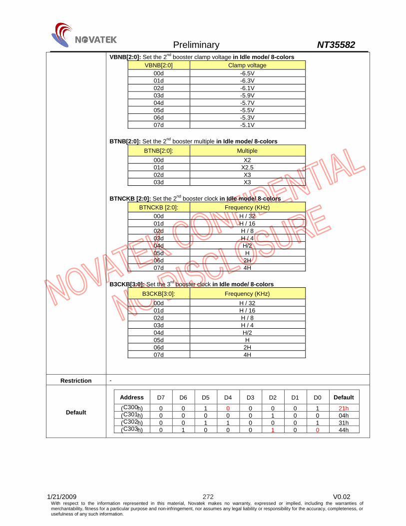
Preliminary NT35582
1/21/2009 272 V0.02 With respect to the information represented in this material, Novatek makes no warranty, expressed or implied, including the warranties of merchantability, fitness for a particular purpose and non-infringement, nor assumes any legal liability or responsibility for the accuracy, completeness, or usefulness of any such information.
VBNB[2:0]: Set the 2nd booster clamp voltage in Idle mode/ 8-colors VBNB[2:0] Clamp voltage
00d -6.5V 01d -6.3V 02d -6.1V 03d -5.9V 04d -5.7V 05d -5.5V 06d -5.3V 07d -5.1V
BTNB[2:0]: Set the 2nd booster multiple in Idle mode/ 8-colors
BTNB[2:0]: Multiple 00d X2 01d X2.5 02d X3 03d X3
BTNCKB [2:0]: Set the 2nd booster clock in Idle mode/ 8-colors
BTNCKB [2:0]: Frequency (KHz) 00d H / 32 01d H / 16 02d H / 8 03d H / 4 04d H/2 05d H 06d 2H 07d 4H
B3CKB[3:0]: Set the 3rd booster clock in Idle mode/ 8-colors
B3CKB[3:0]: Frequency (KHz) 00d H / 32 01d H / 16 02d H / 8 03d H / 4 04d H/2 05d H 06d 2H 07d 4H
Restriction -
Default
Address D7 D6 D5 D4 D3 D2 D1 D0 Default
(C300h) 0 0 1 0 0 0 0 1 21h (C301h) 0 0 0 0 0 1 0 0 04h (C302h) 0 0 1 1 0 0 0 1 31h (C303h) 0 1 0 0 0 1 0 0 44h

Preliminary NT35582
1/21/2009 273 V0.02 With respect to the information represented in this material, Novatek makes no warranty, expressed or implied, including the warranties of merchantability, fitness for a particular purpose and non-infringement, nor assumes any legal liability or responsibility for the accuracy, completeness, or usefulness of any such information.
PWCTR5: Power Control 5 (in Partial mode/ Full-colors) (C400h~C403h) D15 D14 D13 D12 D11 D10 D9 D8 Inst /
Para D7 D6 D5 D4 D3 D2 D1 D0 Code
0 0 0 0 0 0 0 0 Parameter
0 VBPC[2] VBPC[1] VBPC[0] 0 0 BTPC[1] BTPC[0] C400H
0 0 0 0 0 0 0 0 Parameter
0 0 0 0 0 BTPCKC[2]
BTPCKC[1]
BTPCKC[0]
C401H
0 0 0 0 0 0 0 0 Parameter
0 VBNC[2] VBNC[1] VBNC[0] 0 0 BTNC[1] BTNC[0] C402H
0 0 0 0 0 0 0 0 Parameter
0 B3CKC [2]
B3CKC [1]
B3CKC [0] 0 BTNCKC
[2] BTNCKC
[1] BTNCKC
[0] C403H
Note:”-”Don’t care
Description
VBPC[2:0]: Set the 1st booster clamp voltage in Partial mode/ Full-colors
VBPC[2:0] Clamp voltage
00d 6.5V 01d 6.3V 02d 6.1V 03d 5.9V 04d 5.7V 05d 5.5V 06d 5.3V 07d 5.1V
BTPC[2:0]: Set the 1st booster multiple in Partial mode/ Full-colors
BTPC[2:0]: Multiple
00d X2 01d X2.5 02d X3 03d X3
BTPCKC [2:0]: Set the 1st booster clock in Partial mode/ Full-colors
BTPCKC [2:0]: Frequency (KHz)
00d H / 32 01d H / 16 02d H / 8 03d H / 4 04d H/2 05d H 06d 2H 07d 4H

Preliminary NT35582
1/21/2009 274 V0.02 With respect to the information represented in this material, Novatek makes no warranty, expressed or implied, including the warranties of merchantability, fitness for a particular purpose and non-infringement, nor assumes any legal liability or responsibility for the accuracy, completeness, or usefulness of any such information.
VBNC[2:0]: Set the2nd booster clamp voltage in Partial mode/ Full-colors VBNC[2:0] Clamp voltage
00d -6.5V 01d -6.3V 02d -6.1V 03d -5.9V 04d -5.7V 05d -5.5V 06d -5.3V 07d -5.1V
BTNC[2:0]: Set the 2nd booster multiple in Partial mode/ Full-colors
BTNC[2:0] Multiple 00d X2 01d X2.5 02d X3 03d X3
BTNCKC [2:0]: Set the 2nd booster clock in Partial mode/ Full-colors
BTNCKC [2:0] Frequency (KHz) 00d H / 32 01d H / 16 02d H / 8 03d H / 4 04d H/2 05d H 06d 2H 07d 4H
B3CKC[2:0]: Set the 3rd booster clock in Partial mode/ Full-colors
B3CKC [2:0] Frequency (KHz) 00d H / 32 01d H / 16 02d H / 8 03d H / 4 04d H/2 05d H 06d 2H 07d 4H
Restriction -
Default
Address D7 D6 D5 D4 D3 D2 D1 D0 Default (C400h) 0 0 1 0 0 0 0 1 21h (C401h) 0 0 0 0 0 1 0 0 04h (C402h) 0 0 1 1 0 0 0 1 31h (C403h) 0 1 0 0 0 1 0 0 44h

Preliminary NT35582
1/21/2009 275 V0.02 With respect to the information represented in this material, Novatek makes no warranty, expressed or implied, including the warranties of merchantability, fitness for a particular purpose and non-infringement, nor assumes any legal liability or responsibility for the accuracy, completeness, or usefulness of any such information.
VMFCTR: VCOM offset control D15 D14 D13 D12 D11 D10 D9 D8 Inst / Para D7 D6 D5 D4 D3 D2 D1 D0
Code
0 0 0 0 0 0 0 0 VMFCTR/Parameter VM[7] VM[6] VM[5] VM[4] VM[3] VM[2] VM[1] VM[0]
C700H
Note:”-”Don’t care
Description
VCOM offset control: Adjust the offset value of the common voltage for VCOM voltage. VM[7:0]: It can set to MTP 4 times. VCOM voltage offset mode
VM[7:0] VCOM Output voltage
VGMP[7:0](Internal), VGSP[7:0](Internal), VGMN[7:0](Internal), VGSN[7:0](Internal)
00h~02h NOT USE 03h 2.000V 04h 1.984V
: : 7Eh 0.032V 7Fh 0.016V 80h 0V(GND) 81h -0.016V 82h -0.032V
: : FCh -1.984V FDh -2.000V
FEh~FFh NOT USE
NOT CHANGE
Restriction -
Default
Address D7 D6 D5 D4 D3 D2 D1 D0 Default (C700h) 0 1 1 0 1 1 1 1 6Fh

Preliminary NT35582
1/21/2009 276 V0.02 With respect to the information represented in this material, Novatek makes no warranty, expressed or implied, including the warranties of merchantability, fitness for a particular purpose and non-infringement, nor assumes any legal liability or responsibility for the accuracy, completeness, or usefulness of any such information.
RDVMF: Read VCOM offset value (C800h) D15 D14 D13 D12 D11 D10 D9 D8 Inst / Para D7 D6 D5 D4 D3 D2 D1 D0
Code
0 0 0 0 0 0 0 0 RDVMF/Parameter RVM[7] RVM[6] RVM[5] RVM[4] RVM[3] RVM[2] RVM[1] RVM[0]
C800H
Note:”-”Don’t care
Description Read VCOM offset value.
Restriction Read Only
Default Address D7 D6 D5 D4 D3 D2 D1 D0 Default (C701h) 0 1 1 0 1 1 1 1 6Fh
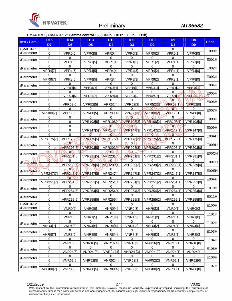
Preliminary NT35582
1/21/2009 277 V0.02 With respect to the information represented in this material, Novatek makes no warranty, expressed or implied, including the warranties of merchantability, fitness for a particular purpose and non-infringement, nor assumes any legal liability or responsibility for the accuracy, completeness, or usefulness of any such information.
GMACTRL1, GMACTRL2: Gamma control 1,2 (E000h~E011h,E100h~E111h) D15 D14 D13 D12 D11 D10 D9 D8 Inst / Para D7 D6 D5 D4 D3 D2 D1 D0
Code
0 0 0 0 0 0 0 0 GMACTRL1 /Parameter 0 VPR0[6] VPR0[5] VPR0[4] VPR0[3] VPR0[2] VPR0[1] VPR0[0]
E000H
0 0 0 0 0 0 0 0 /Parameter 0 VPR1[6] VPR1[5] VPR1[4] VPR1[3] VPR1[2] VPR1[1] VPR1[0]
E001H
0 0 0 0 0 0 0 0 /Parameter VPR4[7] VPR4[6] VPR4[5] VPR4[4] VPR4[3] VPR4[2] VPR4[1] VPR4[0]
E002H
0 0 0 0 0 0 0 0 /Parameter VPR8[7] VPR8[6] VPR8[5] VPR8[4] VPR8[3] VPR8[2] VPR8[1] VPR8[0]
E003H
0 0 0 0 0 0 0 0 /Parameter 0 VPR16[6] VPR16[5] VPR16[4] VPR16[3] VPR16[2] VPR16[1] VPR16[0]
E004H
0 0 0 0 0 0 0 0 /Parameter 0 VPR24[6] VPR24[5] VPR24[4] VPR24[3] VPR24[2] VPR24[1] VPR24[0]
E005H
0 0 0 0 0 0 0 0 /Parameter 0 VPR52[6] VPR52[5] VPR52[4] VPR52[3] VPR52[2] VPR52[1] VPR52[0]
E006H
0 0 0 0 0 0 0 0 /Parameter VPR80[7] VPR80[6] VPR80[5] VPR80[4] VPR80[3] VPR80[2] VPR80[1] VPR80[0]
E007H
0 0 0 0 0 0 0 0 /Parameter 0 0 VPR108[5] VPR108[4] VPR108[3] VPR108[2] VPR108[1] VPR108[0]
E008H
0 0 0 0 0 0 0 0 /Parameter 0 0 VPR147[5] VPR147[4] VPR147[3] VPR147[2] VPR147[1] VPR147[0]
E009H
0 0 0 0 0 0 0 0 /Parameter VPR175[7] VPR175[6] VPR175[5] VPR175[4] VPR175[3] VPR175[2] VPR175[1] VPR175[0]
E00AH
0 0 0 0 0 0 0 0 /Parameter 0 VPR203[6] VPR203[5] VPR203[4] VPR203[3] VPR203[2] VPR203[1] VPR203[0]
E00BH
0 0 0 0 0 0 0 0 /Parameter 0 VPR231[6] VPR231[5] VPR231[4] VPR231[3] VPR231[2] VPR231[1] VPR231[0]
E00CH
0 0 0 0 0 0 0 0 /Parameter 0 VPR239[6] VPR239[5] VPR239[4] VPR239[3] VPR239[2] VPR239[1] VPR239[0]
E00DH
0 0 0 0 0 0 0 0 /Parameter VPR247[7] VPR247[6] VPR247[5] VPR247[4] VPR247[3] VPR247[2] VPR247[1] VPR247[0]
E00EH
0 0 0 0 0 0 0 0 /Parameter VPR251[7] VPR251[6] VPR251[5] VPR251[4] VPR251[3] VPR251[2] VPR251[1] VPR251[0]
E00FH
0 0 0 0 0 0 0 0 /Parameter 0 VPR254[6] VPR254[5] VPR254[4] VPR254[3] VPR254[2] VPR254[1] VPR254[0]
E010H
0 0 0 0 0 0 0 0 /Parameter 0 VPR255[6] VPR255[5] VPR255[4] VPR255[3] VPR255[2] VPR255[1] VPR255[0]
E011H
0 0 0 0 0 0 0 0 GMACTRL2 /Parameter 0 VNR0[6] VNR0[5] VNR0[4] VNR0[3] VNR0[2] VNR0[1] VNR0[0]
E100H
0 0 0 0 0 0 0 0 /Parameter 0 VNR1[6] VNR1[5] VNR1[4] VNR1[3] VNR1[2] VNR1[1] VNR1[0]
E101H
0 0 0 0 0 0 0 0 /Parameter VNR4[7] VNR4[6] VNR4[5] VNR4[4] VNR4[3] VNR4[2] VNR4[1] VNR4[0]
E102H
0 0 0 0 0 0 0 0 /Parameter VNR8[7] VNR8[6] VNR8[5] VNR8[4] VNR8[3] VNR8[2] VNR8[1] VNR8[0]
E103H
0 0 0 0 0 0 0 0 /Parameter 0 VNR16[6] VNR16[5] VNR16[4] VNR16[3] VNR16[2] VNR16[1] VNR16[0]
E104H
0 0 0 0 0 0 0 0 /Parameter 0 VNR24[6] VNR24 [5] VNR24 [4] VNR24 [3] VNR24 [2] VNR24[1] VNR240]
E105H
0 0 0 0 0 0 0 0 /Parameter 0 VNR52[6] VNR52[5] VNR52[4] VNR52[3] VNR52[2] VNR52[1] VNR52[0]
E106H
0 0 0 0 0 0 0 0 /Parameter VNR80[7] VNR80[6] VNR80[5] VNR80[4] VNR80[3] VNR80[2] VNR80[1] VNR80[0]
E107H

Preliminary NT35582
1/21/2009 278 V0.02 With respect to the information represented in this material, Novatek makes no warranty, expressed or implied, including the warranties of merchantability, fitness for a particular purpose and non-infringement, nor assumes any legal liability or responsibility for the accuracy, completeness, or usefulness of any such information.
D15 D14 D13 D12 D11 D10 D9 D8 Inst / Para D7 D6 D5 D4 D3 D2 D1 D0
Code
0 0 0 0 0 0 0 0 /Parameter 0 0 VNR108[5] VNR108[4] VNR108[3] VNR108[2] VNR108[1] VNR108[0]
E108H
0 0 0 0 0 0 0 0 /Parameter 0 0 VNR147[5] VNR147[4] VNR147[3] VNR147[2] VNR147[1] VNR147[0]
E109H
0 0 0 0 0 0 0 0 /Parameter VNR175[7] VNR175[6] VNR175[5] VNR175[4] VNR175[3] VNR175[2] VNR175[1] VNR175[0]
E10AH
0 0 0 0 0 0 0 0 /Parameter 0 VNR203[6] VNR203[5] VNR203[4] VNR203[3] VNR203[2] VNR203[1] VNR203[0]
E10BH
0 0 0 0 0 0 0 0 /Parameter 0 VNR231[6] VNR231[5] VNR231[4] VNR231[3] VNR231[2] VNR231[1] VNR231[0]
E10CH
0 0 0 0 0 0 0 0 /Parameter 0 VNR239[6] VNR239[5] VNR239[4] VNR239[3] VNR239[2] VNR239[1] VNR239[0]
E10DH
0 0 0 0 0 0 0 0 /Parameter VNR247[7] VNR247[6] VNR247[5] VNR247[4] VNR247[3] VNR247[2] VNR247[1] VNR247[0]
E10EH
0 0 0 0 0 0 0 0 /Parameter VNR251[7] VNR251[6] VNR251[5] VNR251[4] VNR251[3] VNR251[2] VNR251[1] VNR251[0]
E10FH
0 0 0 0 0 0 0 0 /Parameter 0 VNR254[6] VNR254[5] VNR254[4] VNR254[3] VNR254[2] VNR254[1] VNR254[0]
E110H
0 0 0 0 0 0 0 0 /Parameter 0 VNR255[6] VNR255[5] VNR255[4] VNR255[3] VNR255[2] VNR255[1] VNR255[0]
E111H
Note:”-”Don’t care
Description These registers are used for gamma correction.
Restriction -
Default
Address Default Address Default (E000h) 00h (E100h) 00h (E001h) 07h (E101h) 06h (E002h) 18h (E102h) 19h (E003h) 29h (E103h) 2Dh (E004h) 1Ch (E104h) 1Ch (E005h) 2Fh (E105h) 2Fh (E006h) 60h (E106h) 61h (E007h) 2Ch (E107h) 3Fh (E008h) 1Fh (E108h) 20h (E009h) 27h (E109h) 27h (E00Ah) 73h (E10Ah) 90h (E00Bh) 13h (E10Bh) 13h (E00Ch) 39h (E10Ch) 3Ah (E00Dh) 4Eh (E10Dh) 4Eh (E00Eh) 72h (E10Eh) 9Eh (E00Fh) 8Fh (E10Fh) BFh (E010h) 2Dh (E110h) 62h (E011h) 32h (E111h) 69h

Preliminary NT35582
1/21/2009 279 V0.02 With respect to the information represented in this material, Novatek makes no warranty, expressed or implied, including the warranties of merchantability, fitness for a particular purpose and non-infringement, nor assumes any legal liability or responsibility for the accuracy, completeness, or usefulness of any such information.
GMACTRL3, GMACTRL4: Gamma control 3,4 (E200h~E211h,E300h~E311h) D15 D14 D13 D12 D11 D10 D9 D8 Inst / Para D7 D6 D5 D4 D3 D2 D1 D0
Code
0 0 0 0 0 0 0 0 GMACTRL3 /Parameter 0 VPG0[6] VPG0[5] VPG0[4] VPG0[3] VPG0[2] VPG0[1] VPG0[0]
E200H
0 0 0 0 0 0 0 0 /Parameter 0 VPG1[6] VPG1[5] VPG1[4] VPG1[3] VPG1[2] VPG1[1] VPG1[0]
E201H
0 0 0 0 0 0 0 0 /Parameter VPG4[7] VPG4[6] VPG4[5] VPG4[4] VPG4[3] VPG4[2] VPG4[1] VPG4[0]
E202H
0 0 0 0 0 0 0 0 /Parameter VPG8[7] VPG8[6] VPG8[5] VPG8[4] VPG8[3] VPG8[2] VPG8[1] VPG8[0]
E203H
0 0 0 0 0 0 0 0 /Parameter 0 VPG16[6] VPG16[5] VPG16[4] VPG16[3] VPG16[2] VPG16[1] VPG16[0]
E204H
0 0 0 0 0 0 0 0 /Parameter 0 VPG24[6] VPG24[5] VPG24[4] VPG24[3] VPG24[2] VPG24[1] VPG24[0]
E205H
0 0 0 0 0 0 0 0 /Parameter 0 VPG52[6] VPG52[5] VPG52[4] VPG52[3] VPG52[2] VPG52[1] VPG52[0]
E206H
0 0 0 0 0 0 0 0 /Parameter VPG80[7] VPG80[6] VPG80[5] VPG80[4] VPG80[3] VPG80[2] VPG80[1] VPG80[0]
E207H
0 0 0 0 0 0 0 0 /Parameter 0 0 VPG108[5] VPG108[4] VPG108[3] VPG108[2] VPG108[1] VPG108[0]
E208H
0 0 0 0 0 0 0 0 /Parameter 0 0 VPG147[5] VPG147[4] VPG147[3] VPG147[2] VPG147[1] VPG147[0]
E209H
0 0 0 0 0 0 0 0 /Parameter VPG175[7] VPG175[6] VPG175[5] VPG175[4] VPG175[3] VPG175[2] VPG175[1] VPG175[0]
E20AH
0 0 0 0 0 0 0 0 /Parameter 0 VPG203[6] VPG203[5] VPG203[4] VPG203[3] VPG203[2] VPG203[1] VPG203[0]
E20BH
0 0 0 0 0 0 0 0 /Parameter 0 VPG231[6] VPG231[5] VPG231[4] VPG231[3] VPG231[2] VPG231[1] VPG231[0]
E20CH
0 0 0 0 0 0 0 0 /Parameter 0 VPG239[6] VPG239[5] VPG239[4] VPG239[3] VPG239[2] VPG239[1] VPG239[0]
E20DH
0 0 0 0 0 0 0 0 /Parameter VPG247[7] VPG247[6] VPG247[5] VPG247[4] VPG247[3] VPG247[2] VPG247[1] VPG247[0]
E20EH
0 0 0 0 0 0 0 0 /Parameter VPG251[7] VPG251[6] VPG251[5] VPG251[4] VPG251[3] VPG251[2] VPG251[1] VPG251[0]
E20FH
0 0 0 0 0 0 0 0 /Parameter 0 VPG254[6] VPG254[5] VPG254[4] VPG254[3] VPG254[2] VPG254[1] VPG254[0]
E210H
0 0 0 0 0 0 0 0 /Parameter 0 VPG255[6] VPG255[5] VPG255[4] VPG255[3] VPG255[2] VPG255[1] VPG255[0]
E211H
0 0 0 0 0 0 0 0 GMACTRL4 /Parameter 0 VNG0[6] VNG0[5] VNG0[4] VNG0[3] VNG0[2] VNG0[1] VNG0[0]
E300H
0 0 0 0 0 0 0 0 /Parameter 0 VNG1[6] VNG1[5] VNG1[4] VNG1[3] VNG1[2] VNG1[1] VNG1[0]
E301H
0 0 0 0 0 0 0 0 /Parameter VNG4[7] VNG4[6] VNG4[5] VNG4[4] VNG4[3] VNG4[2] VNG4[1] VNG4[0]
E302H
0 0 0 0 0 0 0 0 /Parameter VNG8[7] VNG8[6] VNG8[5] VNG8[4] VNG8[3] VNG8[2] VNG8[1] VNG8[0]
E303H
0 0 0 0 0 0 0 0 /Parameter 0 VNG16[6] VNG16[5] VNG16[4] VNG16[3] VNG16[2] VNG16[1] VNG16[0]
E304H
0 0 0 0 0 0 0 0 /Parameter 0 VNG24[6] VNG24 [5] VNG24 [4] VNG24 [3] VNG24 [2] VNG24[1] VNG240]
E305H
0 0 0 0 0 0 0 0 /Parameter 0 VNG52[6] VNG52[5] VNG52[4] VNG52[3] VNG52[2] VNG52[1] VNG52[0]
E306H
0 0 0 0 0 0 0 0 /Parameter VNG80[7] VNG80[6] VNG80[5] VNG80[4] VNG80[3] VNG80[2] VNG80[1] VNG80[0]
E307H
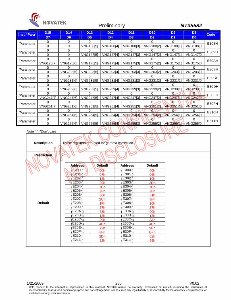
Preliminary NT35582
1/21/2009 280 V0.02 With respect to the information represented in this material, Novatek makes no warranty, expressed or implied, including the warranties of merchantability, fitness for a particular purpose and non-infringement, nor assumes any legal liability or responsibility for the accuracy, completeness, or usefulness of any such information.
D15 D14 D13 D12 D11 D10 D9 D8 Inst / Para D7 D6 D5 D4 D3 D2 D1 D0
Code
0 0 0 0 0 0 0 0 /Parameter 0 0 VNG108[5] VNG108[4] VNG108[3] VNG108[2] VNG108[1] VNG108[0]
E308H
0 0 0 0 0 0 0 0 /Parameter 0 0 VNG147[5] VNG147[4] VNG147[3] VNG147[2] VNG147[1] VNG147[0]
E309H
0 0 0 0 0 0 0 0 /Parameter VNG175[7] VNG175[6] VNG175[5] VNG175[4] VNG175[3] VNG175[2] VNG175[1] VNG175[0]
E30AH
0 0 0 0 0 0 0 0 /Parameter 0 VNG203[6] VNG203[5] VNG203[4] VNG203[3] VNG203[2] VNG203[1] VNG203[0]
E30BH
0 0 0 0 0 0 0 0 /Parameter 0 VNG231[6] VNG231[5] VNG231[4] VNG231[3] VNG231[2] VNG231[1] VNG231[0]
E30CH
0 0 0 0 0 0 0 0 /Parameter 0 VNG239[6] VNG239[5] VNG239[4] VNG239[3] VNG239[2] VNG239[1] VNG239[0]
E30DH
0 0 0 0 0 0 0 0 /Parameter VNG247[7] VNG247[6] VNG247[5] VNG247[4] VNG247[3] VNG247[2] VNG247[1] VNG247[0]
E30EH
0 0 0 0 0 0 0 0 /Parameter VNG251[7] VNG251[6] VNG251[5] VNG251[4] VNG251[3] VNG251[2] VNG251[1] VNG251[0]
E30FH
0 0 0 0 0 0 0 0 /Parameter 0 VNG254[6] VNG254[5] VNG254[4] VNG254[3] VNG254[2] VNG254[1] VNG254[0]
E310H
0 0 0 0 0 0 0 0 /Parameter 0 VNG255[6] VNG255[5] VNG255[4] VNG255[3] VNG255[2] VNG255[1] VNG255[0]
E311H
Note:”-”Don’t care
Description These registers are used for gamma correction.
Restriction -
Default
Address Default Address Default (E200h) 00h (E300h) 00h (E201h) 07h (E301h) 06h (E202h) 18h (E302h) 19h (E203h) 29h (E303h) 2Dh (E204h) 1Ch (E304h) 1Ch (E205h) 2Fh (E305h) 2Fh (E206h) 60h (E306h) 61h (E207h) 2Ch (E307h) 3Fh (E208h) 1Fh (E308h) 20h (E209h) 27h (E309h) 27h (E20Ah) 73h (E30Ah) 90h (E20Bh) 13h (E30Bh) 13h (E20Ch) 39h (E30Ch) 3Ah (E20Dh) 4Eh (E30Dh) 4Eh (E20Eh) 72h (E30Eh) 9Eh (E20Fh) 8Fh (E30Fh) BFh (E210h) 2Dh (E310h) 62h (E211h) 32h (E311h) 69h

Preliminary NT35582
1/21/2009 281 V0.02 With respect to the information represented in this material, Novatek makes no warranty, expressed or implied, including the warranties of merchantability, fitness for a particular purpose and non-infringement, nor assumes any legal liability or responsibility for the accuracy, completeness, or usefulness of any such information.
GMACTRL5, GMACTRL6: Gamma control 5,6 (E400h~E411h,E500h~E511h) D15 D14 D13 D12 D11 D10 D9 D8 Inst / Para D7 D6 D5 D4 D3 D2 D1 D0
Code
0 0 0 0 0 0 0 0 GMACTRL5 /Parameter 0 VPB0[6] VPB0[5] VPB0[4] VPB0[3] VPB0[2] VPB0[1] VPB0[0]
E400H
0 0 0 0 0 0 0 0 /Parameter 0 VPB1[6] VPB1[5] VPB1[4] VPB1[3] VPB1[2] VPB1[1] VPB1[0]
E401H
0 0 0 0 0 0 0 0 /Parameter VPB4[7] VPB4[6] VPB4[5] VPB4[4] VPB4[3] VPB4[2] VPB4[1] VPB4[0]
E402H
0 0 0 0 0 0 0 0 /Parameter VPB8[7] VPB8[6] VPB8[5] VPB8[4] VPB8[3] VPB8[2] VPB8[1] VPB8[0]
E403H
0 0 0 0 0 0 0 0 /Parameter 0 VPB16[6] VPB16[5] VPB16[4] VPB16[3] VPB16[2] VPB16[1] VPB16[0]
E404H
0 0 0 0 0 0 0 0 /Parameter 0 VPB24[6] VPB24[5] VPB24[4] VPB24[3] VPB24[2] VPB24[1] VPB24[0]
E405H
0 0 0 0 0 0 0 0 /Parameter 0 VPB52[6] VPB52[5] VPB52[4] VPB52[3] VPB52[2] VPB52[1] VPB52[0]
E406H
0 0 0 0 0 0 0 0 /Parameter VPB80[7] VPB80[6] VPB80[5] VPB80[4] VPB80[3] VPB80[2] VPB80[1] VPB80[0]
E407H
0 0 0 0 0 0 0 0 /Parameter 0 0 VPB108[5] VPB108[4] VPB108[3] VPB108[2] VPB108[1] VPB108[0]
E408H
0 0 0 0 0 0 0 0 /Parameter 0 0 VPB147[5] VPB147[4] VPB147[3] VPB147[2] VPB147[1] VPB147[0]
E409H
0 0 0 0 0 0 0 0 /Parameter VPB175[7] VPB175[6] VPB175[5] VPB175[4] VPB175[3] VPB175[2] VPB175[1] VPB175[0]
E40AH
0 0 0 0 0 0 0 0 /Parameter 0 VPB203[6] VPB203[5] VPB203[4] VPB203[3] VPB203[2] VPB203[1] VPB203[0]
E40BH
0 0 0 0 0 0 0 0 /Parameter 0 VPB231[6] VPB231[5] VPB231[4] VPB231[3] VPB231[2] VPB231[1] VPB231[0]
E40CH
0 0 0 0 0 0 0 0 /Parameter 0 VPB239[6] VPB239[5] VPB239[4] VPB239[3] VPB239[2] VPB239[1] VPB239[0]
E40DH
0 0 0 0 0 0 0 0 /Parameter VPB247[7] VPB247[6] VPB247[5] VPB247[4] VPB247[3] VPB247[2] VPB247[1] VPB247[0]
E40EH
0 0 0 0 0 0 0 0 /Parameter VPB251[7] VPB251[6] VPB251[5] VPB251[4] VPB251[3] VPB251[2] VPB251[1] VPB251[0]
E40FH
0 0 0 0 0 0 0 0 /Parameter 0 VPB254[6] VPB254[5] VPB254[4] VPB254[3] VPB254[2] VPB254[1] VPB254[0]
E410H
0 0 0 0 0 0 0 0 /Parameter 0 VPB255[6] VPB255[5] VPB255[4] VPB255[3] VPB255[2] VPB255[1] VPB255[0]
E411H
0 0 0 0 0 0 0 0 GMACTRL6 /Parameter 0 VNB0[6] VNB0[5] VNB0[4] VNB0[3] VNB0[2] VNB0[1] VNB0[0]
E500H
0 0 0 0 0 0 0 0 /Parameter 0 VNB1[6] VNB1[5] VNB1[4] VNB1[3] VNB1[2] VNB1[1] VNB1[0]
E501H
0 0 0 0 0 0 0 0 /Parameter VNB4[7] VNB4[6] VNB4[5] VNB4[4] VNB4[3] VNB4[2] VNB4[1] VNB4[0]
E502H
0 0 0 0 0 0 0 0 /Parameter VNB8[7] VNB8[6] VNB8[5] VNB8[4] VNB8[3] VNB8[2] VNB8[1] VNB8[0]
E503H
0 0 0 0 0 0 0 0 /Parameter 0 VNB16[6] VNB16[5] VNB16[4] VNB16[3] VNB16[2] VNB16[1] VNB16[0]
E504H
0 0 0 0 0 0 0 0 /Parameter 0 VNB24[6] VNB24 [5] VNB24 [4] VNB24 [3] VNB24 [2] VNB24[1] VNB240]
E505H
0 0 0 0 0 0 0 0 /Parameter 0 VNB52[6] VNB52[5] VNB52[4] VNB52[3] VNB52[2] VNB52[1] VNB52[0]
E506H
0 0 0 0 0 0 0 0 /Parameter VNB80[7] VNB80[6] VNB80[5] VNB80[4] VNB80[3] VNB80[2] VNB80[1] VNB80[0]
E507H

Preliminary NT35582
1/21/2009 282 V0.02 With respect to the information represented in this material, Novatek makes no warranty, expressed or implied, including the warranties of merchantability, fitness for a particular purpose and non-infringement, nor assumes any legal liability or responsibility for the accuracy, completeness, or usefulness of any such information.
D15 D14 D13 D12 D11 D10 D9 D8 Inst / Para D7 D6 D5 D4 D3 D2 D1 D0
Code
0 0 0 0 0 0 0 0 /Parameter 0 0 VNB108[5] VNB108[4] VNB108[3] VNB108[2] VNB108[1] VNB108[0]
E508H
0 0 0 0 0 0 0 0 /Parameter 0 0 VNB147[5] VNB147[4] VNB147[3] VNB147[2] VNB147[1] VNB147[0]
E509H
0 0 0 0 0 0 0 0 /Parameter VNB175[7] VNB175[6] VNB175[5] VNB175[4] VNB175[3] VNB175[2] VNB175[1] VNB175[0]
E50AH
0 0 0 0 0 0 0 0 /Parameter 0 VNB203[6] VNB203[5] VNB203[4] VNB203[3] VNB203[2] VNB203[1] VNB203[0]
E50BH
0 0 0 0 0 0 0 0 /Parameter 0 VNB231[6] VNB231[5] VNB231[4] VNB231[3] VNB231[2] VNB231[1] VNB231[0]
E50CH
0 0 0 0 0 0 0 0 /Parameter 0 VNB239[6] VNB239[5] VNB239[4] VNB239[3] VNB239[2] VNB239[1] VNB239[0]
E50DH
0 0 0 0 0 0 0 0 /Parameter VNB247[7] VNB247[6] VNB247[5] VNB247[4] VNB247[3] VNB247[2] VNB247[1] VNB247[0]
E50EH
0 0 0 0 0 0 0 0 /Parameter VNB251[7] VNB251[6] VNB251[5] VNB251[4] VNB251[3] VNB251[2] VNB251[1] VNB251[0]
E50FH
0 0 0 0 0 0 0 0 /Parameter 0 VNB254[6] VNB254[5] VNB254[4] VNB254[3] VNB254[2] VNB254[1] VNB254[0]
E510H
0 0 0 0 0 0 0 0 /Parameter 0 VNB255[6] VNB255[5] VNB255[4] VNB255[3] VNB255[2] VNB255[1] VNB255[0]
E511H
Note:”-”Don’t care
Description These registers are used for gamma correction.
Restriction -
Default
Address Default Address Default (E400h) 00h (E500h) 00h (E401h) 07h (E501h) 06h (E402h) 18h (E502h) 19h (E403h) 29h (E503h) 2Dh (E404h) 1Ch (E504h) 1Ch (E405h) 2Fh (E505h) 2Fh (E406h) 60h (E506h) 61h (E407h) 2Ch (E507h) 3Fh (E408h) 1Fh (E508h) 20h (E409h) 27h (E509h) 27h (E40Ah) 73h (E50Ah) 90h (E40Bh) 13h (E50Bh) 13h (E40Ch) 39h (E50Ch) 3Ah (E40Dh) 4Eh (E50Dh) 4Eh (E40Eh) 72h (E50Eh) 9Eh (E40Fh) 8Fh (E50Fh) BFh (E410h) 2Dh (E510h) 62h (E411h) 32h (E511h) 69h

Preliminary NT35582
1/21/2009 283 V0.02 With respect to the information represented in this material, Novatek makes no warranty, expressed or implied, including the warranties of merchantability, fitness for a particular purpose and non-infringement, nor assumes any legal liability or responsibility for the accuracy, completeness, or usefulness of any such information.
RDDID: Device code read (1080h~1180h) D15 D14 D13 D12 D11 D10 D9 D8 Inst / Para D7 D6 D5 D4 D3 D2 D1 D0
Code
0 0 0 0 0 0 0 0 Parameter 0 1 0 1 0 1 0 1
1080h
0 0 0 0 0 0 0 0 Parameter 1 0 0 0 0 0 1 0
1180h
Note:”-”Don’t care
Description Device code “5582”H will be read out when this register is read out forcibly.
Restriction Read Only
Default
1080h=0x0055h D15 D14 D13 D12 D11 D10 D09 D08
0 0 0 0 0 0 0 0 D07 D06 D05 D04 D03 D02 D01 D00
0 1 0 1 0 1 0 1 1180h=0x0082h
D15 D14 D13 D12 D11 D10 D09 D08 0 0 0 0 0 0 0 0
D07 D06 D05 D04 D03 D02 D01 D00 1 0 0 0 0 0 1 0

Preliminary NT35582
1/21/2009 284 V0.02 With respect to the information represented in this material, Novatek makes no warranty, expressed or implied, including the warranties of merchantability, fitness for a particular purpose and non-infringement, nor assumes any legal liability or responsibility for the accuracy, completeness, or usefulness of any such information.
USERID: User ID Code Control (1280h) D15 D14 D13 D12 D11 D10 D9 D8 Inst / Para D7 D6 D5 D4 D3 D2 D1 D0
Code
0 0 0 0 0 0 0 0 Parameter 0 ID [6] ID [5] ID [4] ID [3] ID [2] ID [1] ID [0]
1280h
Note:”-”Don’t care
Description ID[6:0]: Write these bits of user ID code to save it to NV memory.
Restriction -
Default
D15 D14 D13 D12 D11 D10 D09 D08 0 0 0 0 0 0 0 0
D07 D06 D05 D04 D03 D02 D01 D00 0 0 0 0 0 0 0 0

Preliminary NT35582
1/21/2009 285 V0.02 With respect to the information represented in this material, Novatek makes no warranty, expressed or implied, including the warranties of merchantability, fitness for a particular purpose and non-infringement, nor assumes any legal liability or responsibility for the accuracy, completeness, or usefulness of any such information.
REVISIONID: Revision ID Code (1380h) D15 D14 D13 D12 D11 D10 D9 D8 Inst / Para D7 D6 D5 D4 D3 D2 D1 D0
Code
0 0 0 0 0 0 0 0 Parameter 0 0 0 0 VER[3] VER[2] VER[1] VER[0]
1380h
Note:”-”Don’t care
Description VER[3:0]: These bits are driver IC version. The revision number is swollen according to the revision.
Restriction Read Only
Default
D15 D14 D13 D12 D11 D10 D09 D08 0 0 0 0 0 0 0 0
D07 D06 D05 D04 D03 D02 D01 D00 0 0 0 0 0 0 0 0
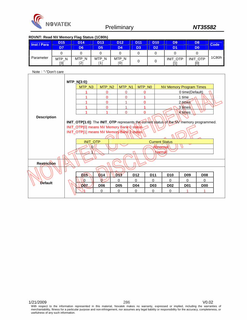
Preliminary NT35582
1/21/2009 286 V0.02 With respect to the information represented in this material, Novatek makes no warranty, expressed or implied, including the warranties of merchantability, fitness for a particular purpose and non-infringement, nor assumes any legal liability or responsibility for the accuracy, completeness, or usefulness of any such information.
RDVNT: Read NV Memory Flag Status (1C80h) D15 D14 D13 D12 D11 D10 D9 D8 Inst / Para D7 D6 D5 D4 D3 D2 D1 D0
Code
0 0 0 0 0 0 0 0 Parameter MTP_N
[3] MTP_N
[2] MTP_N
[1] MTP_N
[0] 0 0 INIT_OTP [1]
INIT_OTP [0]
1C80h
Note:”-”Don’t care
Description
MTP_N[3:0]:
MTP_N3 MTP_N2 MTP_N1 MTP_N0 NV Memory Program Times 1 0 0 0 0 time(Default) 1 0 0 1 1 time 1 0 1 0 2 times 1 0 1 1 3 times 1 1 0 0 4 times
INIT_OTP[1:0]: The INIT_OTP represents the current status of the NV memory programmed. INIT_OTP[0] means NV Memory Bank 0 status. INIT_OTP[1] means NV Memory Bank 1 status.
INIT_OTP Current Status 0 Abnormal 1 Normal
Restriction -
Default
D15 D14 D13 D12 D11 D10 D09 D08 0 0 0 0 0 0 0 0
D07 D06 D05 D04 D03 D02 D01 D00 1 0 0 0 0 0 1 1
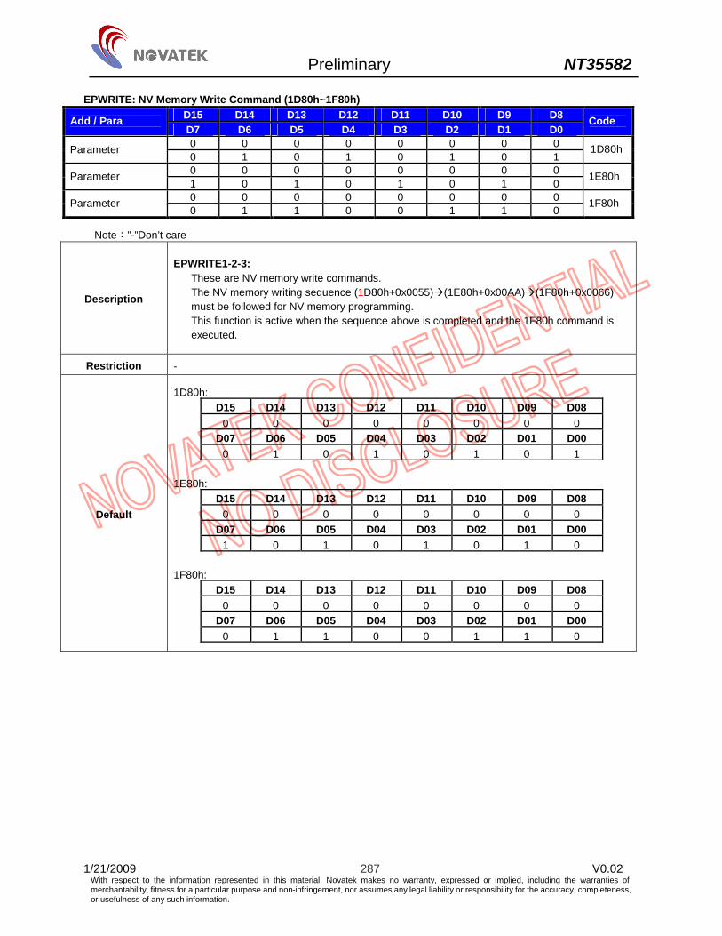
Preliminary NT35582
1/21/2009 287 V0.02 With respect to the information represented in this material, Novatek makes no warranty, expressed or implied, including the warranties of merchantability, fitness for a particular purpose and non-infringement, nor assumes any legal liability or responsibility for the accuracy, completeness, or usefulness of any such information.
EPWRITE: NV Memory Write Command (1D80h~1F80h) D15 D14 D13 D12 D11 D10 D9 D8 Add / Para D7 D6 D5 D4 D3 D2 D1 D0
Code
0 0 0 0 0 0 0 0 Parameter 0 1 0 1 0 1 0 1
1D80h
0 0 0 0 0 0 0 0 Parameter 1 0 1 0 1 0 1 0
1E80h
0 0 0 0 0 0 0 0 Parameter 0 1 1 0 0 1 1 0
1F80h
Note:”-”Don’t care
Description
EPWRITE1-2-3: These are NV memory write commands. The NV memory writing sequence (1D80h+0x0055)(1E80h+0x00AA)(1F80h+0x0066) must be followed for NV memory programming. This function is active when the sequence above is completed and the 1F80h command is executed.
Restriction -
Default
1D80h: D15 D14 D13 D12 D11 D10 D09 D08
0 0 0 0 0 0 0 0 D07 D06 D05 D04 D03 D02 D01 D00
0 1 0 1 0 1 0 1 1E80h:
D15 D14 D13 D12 D11 D10 D09 D08 0 0 0 0 0 0 0 0
D07 D06 D05 D04 D03 D02 D01 D00 1 0 1 0 1 0 1 0
1F80h:
D15 D14 D13 D12 D11 D10 D09 D08 0 0 0 0 0 0 0 0
D07 D06 D05 D04 D03 D02 D01 D00 0 1 1 0 0 1 1 0
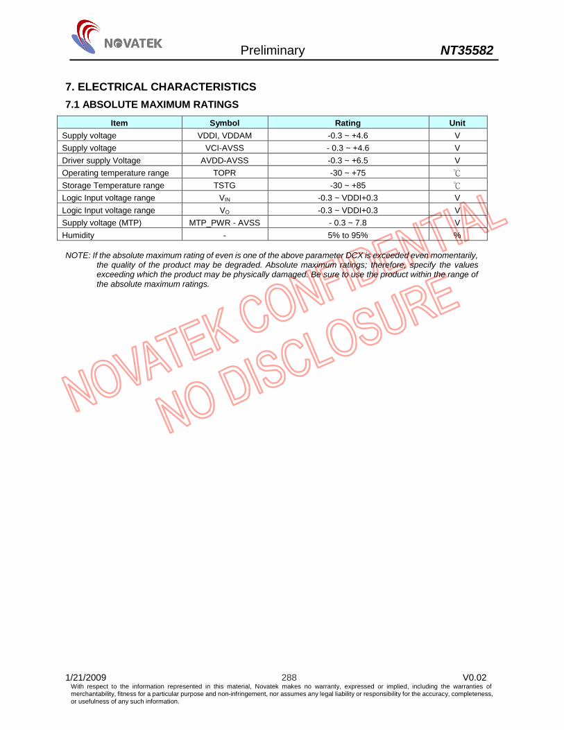
Preliminary NT35582
1/21/2009 288 V0.02 With respect to the information represented in this material, Novatek makes no warranty, expressed or implied, including the warranties of merchantability, fitness for a particular purpose and non-infringement, nor assumes any legal liability or responsibility for the accuracy, completeness, or usefulness of any such information.
7. ELECTRICAL CHARACTERISTICS 7.1 ABSOLUTE MAXIMUM RATINGS
Item Symbol Rating Unit Supply voltage VDDI, VDDAM -0.3 ~ +4.6 V Supply voltage VCI-AVSS - 0.3 ~ +4.6 V Driver supply Voltage AVDD-AVSS -0.3 ~ +6.5 V Operating temperature range TOPR -30 ~ +75 Storage Temperature range TSTG -30 ~ +85 Logic Input voltage range VIN -0.3 ~ VDDI+0.3 V Logic Input voltage range VO -0.3 ~ VDDI+0.3 V Supply voltage (MTP) MTP_PWR - AVSS - 0.3 ~ 7.8 V Humidity - 5% to 95% % NOTE: If the absolute maximum rating of even is one of the above parameter DCX is exceeded even momentarily,
the quality of the product may be degraded. Absolute maximum ratings; therefore, specify the values exceeding which the product may be physically damaged. Be sure to use the product within the range of the absolute maximum ratings.

Preliminary NT35582
1/21/2009 289 V0.02 With respect to the information represented in this material, Novatek makes no warranty, expressed or implied, including the warranties of merchantability, fitness for a particular purpose and non-infringement, nor assumes any legal liability or responsibility for the accuracy, completeness, or usefulness of any such information.
7.2 DC CHARACTERISTICS 7.2.1 Basic Characteristics
Specification Parameter Symbol Conditions MIN TYP MAX
Unit Notes
Power & Operation Voltage Analog Operating voltage VCI Operating Voltage 2.5 2.85 3.3 V Note 2
V I/O operating voltage (Except MDDI)
VDDI I/O supply voltage 1.65 2.6 3.3 V
Note 2
MDDI Operating voltage VDDAM MDDI supply voltage 2.5 2.85 3.3 V Note 2 Input / Output
Logic High level input voltage VIH - 0.7*VDDI - VDDI V Note 1, 2, 3 Logic Low level input voltage VIL - VSS - 0.3*VDDI V Note 1, 2, 3 Logic High level output voltage VOH IOH = -0.1mA 0.8*VDDI - VDDI V Note 1, 2, 3 Logic Low level output voltage VOL IOL = +0.1mA VSS - 0.2*VDDI V Note 1, 2, 3 Logic High level leakage (Except MDDI)
ILIH1 Vin = 0 to VDDI - - 1 µA Note 1, 2, 3
Logic Low level leakage (Except MDDI)
ILIL1 Vin = 0 to VDDI -1 - - µA Note 1, 2, 3
Logic High level leakage (MDDI)
ILIH2 Vin = 0 to VDDAM - - 1 µA Note 2,9
Logic Low level leakage (MDDI)
ILIL2 Vin = 0 to VDDAM -1 - - µA Note 2,9
VCOM Operation VCOM voltage VCOM Operating Voltage -2.0 - 2.0 V Note 3
Source Driver Gamma reference voltage 3.0 5.5 V Note 3
Output deviation voltage Vdev Sout>=4.2V,Sout<=0.
8V 30 mV
Output deviation voltage Vdev 4.2V>Sout>0.8V 20 mV Note 5
Output offset voltage VOFSET 35 mV Note 8 Booster Operation
Internal reference voltage VREF -1 1 V Note 3 1st Booster voltage AVDD 5.8 6.5 V Note 6 2nd Booster voltage AVEE -6.5 -5.8 V Note 6 3rd Booster voltage VCL -VCI V Note 6
4th Booster voltage VGH AVDD+VCI - 2*AVDD-AVEE
V -
5th Booster voltage VGL 2*AVEE-AV
DD - VCL+AVE
E V -
Note 1: VDDI=1.65 to 3.3V, VCI=VDDAM=2.5 to 3.3V, AVSS=VSS=AVSSR=0V, Ta=-30 to 70 (to +85 no damage)
Note 2, 3, 4: When the measurements are performed with LCD module, measurement points are like below. CSX, RDX, WRX, D[23:0], DCX, RESX, SCL, IM[2:0] and Test pins
Note 5: Source channel loading = 40pF/channel Note 6: VCI=2.85V, Ta=25 , No load on the panel, Iload1 = -2[mA] Note 7: VCI=2.85V, Ta=25 , No load on the panel, Iload1 = -2[mA] Note 8: The max. value is between Note 4 measure point and Gamma setting value. Note 9: Vin = 0 to VDDAM, VDDAM=2.5 to 3.3V, VCC=1.4 to 1.6V, VCI=2.5 to 3.3V,
VG_MDDI=AVSS=VSS=AVSSR=0V, Ta=-30 to 70 (to +85 no damage)

Preliminary NT35582
1/21/2009 290 V0.02 With respect to the information represented in this material, Novatek makes no warranty, expressed or implied, including the warranties of merchantability, fitness for a particular purpose and non-infringement, nor assumes any legal liability or responsibility for the accuracy, completeness, or usefulness of any such information.
7.2.2 Current Consumption
Specification Parameter Symbol Conditions MIN TYP MAX
Unit
Normal operation IOPA
VDDI=2.6V, VCI=VDDAM=2.85 V, VCC=1.5V 864 lines, Ta = 25°C, fFLM = 60Hz, RAM data: 18h’00000
- - 65 mW
Sleep in mode ISPA VDDI=2.6V, VCI=VDDAM=2.85 V, VCC=1.5V 864 lines, Ta = 25°C
- 80 160 μA
Deep standby mode IDST VDDI=2.6V, VCI=VDDAM=2.85 V, VCC=1.5V, Ta = 25°C - 2 5 μA
7.2.3 MDDI DC Characteristics
Specification Parameter Symbol Conditions MIN TYP MAX
Unit
Differential input “High” level voltage (VT=125mV) (MDDI_DATA_P/M) VIT+off - 125 175 mV
Differential input “Low” level voltage (VT=125mV) (MDDI_DATA_P/M) VIT-off 75 125 - mV
Differential input “High” level voltage (VT=0) (MDDI_DATA_P/M, MDDI_STB_P/M)
VIT+ - 0 50 mV
Differential input “Low” level voltage (VT=0) (MDDI_DATA_P/M, MDDI_STB_P/M)
VIT+ -50 0 - mV
Current consumption (VDDAM-VSS) in Hibernation Ihib
VDDI=2.6V, VCI=VDDAM= 2.85V, VCC=1.5V, 1/tBIT=384Mbps, Ta=25
- T.B.D - μA
Current consumption (VDDAM-VSS) in data transfer Itrans
VDDI=2.6V, VCI=VDDAM=2.85V, VCC=1.5V, In Video Stream Packet Transfer, 1/tBIT=384Mbps, Ta=25 ,
- T.B.D - mA

Preliminary NT35582
1/21/2009 291 V0.02 With respect to the information represented in this material, Novatek makes no warranty, expressed or implied, including the warranties of merchantability, fitness for a particular purpose and non-infringement, nor assumes any legal liability or responsibility for the accuracy, completeness, or usefulness of any such information.
7.3 AC CHARACTERISTICS 7.3.1 80-System Bus Interface Timing Characteristics (24-/16-/8-bit Transfer Mode)
Figure.110 80-System Bus Interface Operation
Table 7.3.1 VDDI=1.65~3.3, VCI=2.5~3.3 (Register Access)
Item Symbol Timing Diagram Min Typ Max Unit
Write cycle time tWC Figure.110 66 - - ns
Read cycle time tRC Figure.110 160 - - ns
Write control pulse “Low” duration tWRL Figure.110 33 - - ns
Read control pulse “Low” duration tRDL Figure.110 45 - - ns
Write control pulse “High” duration tWRH Figure.110 33 - - ns
Read control pulse “High” duration tRDH Figure.110 90 - - ns
Write setup time (DCX to CSX, WRX) tAST Figure.110 0 - - ns
Read setup time (DCX to CSX, RDX) tAST Figure.110 10 - ns
Address hold time tAHT Figure.110 2 - - ns
Write data setup time tDST Figure.110 15 - - ns
Write data hold time tDHT Figure.110 10 - - ns
Read data access time tRAT Figure.110 - - 40 ns
Read data hold time tODH Figure.110 5 - - ns

Preliminary NT35582
1/21/2009 292 V0.02 With respect to the information represented in this material, Novatek makes no warranty, expressed or implied, including the warranties of merchantability, fitness for a particular purpose and non-infringement, nor assumes any legal liability or responsibility for the accuracy, completeness, or usefulness of any such information.
7.3.2 80-System Bus Interface Timing Characteristics (24-bit Transfer Mode)
Table 7.3.2.1 High-speed Write Mode (HSM = 1), VDDI=1.65~3.3, VCI=2.5~3.3 (RAM Data Access)
Item Symbol Timing Diagram Min. Typ. Max. Unit
Write cycle time tWC Figure.110 33 - - ns
Read cycle time tRCFM Figure.110 400 - ns
Write low-level pulse width tWRL Figure.110 15 - - ns
Read low-level pulse width tRDLFM Figure.110 150 - - ns
Write high-level pulse width tWRH Figure.110 15 - - ns
Read high-level pulse width tRDHFM Figure.110 250 - - ns
Write setup time (DCX to CSX, WRX) tAST Figure.110 0 - - ns
Read setup time (DCX to CSX, RDX) tAST Figure.110 10 - ns
Address hold time tAHT Figure.110 2 - - ns
Write data setup time tDST Figure.110 10 - ns
Write data hold time tDHT Figure.110 10 - - ns
Read data delay time tRATFM Figure.110 - - 150 ns
Read data hold time tODH Figure.110 5 - - ns
Table 7.3.2.2 Normal Write Mode (HSM = 0), VDDI=1.65~3.3, VCI=2.5~3.3 (RAM Data Access)
Item Symbol Timing Diagram Min. Typ. Max. Unit
Write cycle time tWC Figure.110 66 - - ns
Read cycle time tRCFM Figure.110 400 - - ns
Write low-level pulse width tWRL Figure.110 30 - - ns
Read low-level pulse width tRDLFM Figure.110 150 - ns
Write high-level pulse width tWRH Figure.110 30 - - ns
Read high-level pulse width tRDHFM Figure.110 250 - - ns
Write setup time (DCX to CSX, WRX) tAST Figure.110 0 - - ns
Read setup time (DCX to CSX, RDX) tAST Figure.110 10 - ns
Address hold time tAHT Figure.110 2 - - ns
Write data setup time tDST Figure.110 15 - - ns
Write data hold time tDHT Figure.110 10 - - ns
Read data delay time tRATFM Figure.110 - - 150 ns
Read data hold time tODH Figure.110 5 - - ns

Preliminary NT35582
1/21/2009 293 V0.02 With respect to the information represented in this material, Novatek makes no warranty, expressed or implied, including the warranties of merchantability, fitness for a particular purpose and non-infringement, nor assumes any legal liability or responsibility for the accuracy, completeness, or usefulness of any such information.
7.3.3 80-System Bus Interface Timing Characteristics (16-bit / 8-bit Transfer Mode)
Table 7.3.3.1 High-speed Write Mode (HSM = 1), VDDI=1.65~3.3, VCI=2.5~3.3 (RAM Data Access)
Item Symbol Timing Diagram Min. Typ. Max. Unit
Write cycle time tWC Figure.110 33 - - ns
Read cycle time tRCFM Figure.110 400 - ns
Write low-level pulse width tWRL Figure.110 15 - - ns
Read low-level pulse width tRDLFM Figure.110 150 - - ns
Write high-level pulse width tWRH Figure.110 15 - - ns
Read high-level pulse width tRDHFM Figure.110 250 - - ns
Write setup time (DCX to CSX, WRX) tAST Figure.110 0 - - ns
Read setup time (DCX to CSX, RDX) tAST Figure.110 10 - ns
Address hold time tAHT Figure.110 2 - - ns
Write data setup time tDST Figure.110 10 - ns
Write data hold time tDHT Figure.110 10 - - ns
Read data delay time tRATFM Figure.110 - - 150 ns
Read data hold time tODH Figure.110 5 - - ns
Table 7.3.3.2 Normal Write Mode (HSM = 0), VDDI=1.65~3.3, VCI=2.5~3.3 (RAM Data Access)
Item Symbol Timing Diagram Min. Typ. Max. Unit
Write cycle time tWC Figure.110 33 - - ns
Read cycle time tRCFM Figure.110 400 - - ns
Write low-level pulse width tWRL Figure.110 30 - - ns
Read low-level pulse width tRDLFM Figure.110 150 - ns
Write high-level pulse width tWRH Figure.110 30 - - ns
Read high-level pulse width tRDHFM Figure.110 250 - - ns
Write setup time (DCX to CSX, WRX) tAST Figure.110 0 - - ns
Read setup time (DCX to CSX, RDX) tAST Figure.110 10 - ns
Address hold time tAHT Figure.110 2 - - ns
Write data setup time tDST Figure.110 15 - - ns
Write data hold time tDHT Figure.110 10 - - ns
Read data delay time tRATFM Figure.110 - - 150 ns
Read data hold time tODH Figure.110 5 - - ns

Preliminary NT35582
1/21/2009 294 V0.02 With respect to the information represented in this material, Novatek makes no warranty, expressed or implied, including the warranties of merchantability, fitness for a particular purpose and non-infringement, nor assumes any legal liability or responsibility for the accuracy, completeness, or usefulness of any such information.
7.3.4 Serial Interface Timing Characteristics
tCSS
VIH
VIL
tSDS tSDH
tSHW/tSHR
tSCYCW/tSCYCRtCHW
tCSH
tSLW/tSLR
tf tr
tACC tOH
CSX
WRX/SCL
SDI
SDO
Figure.111 Serial Interface Operation
Table 7.3.4.1 Normal/High-speed Write Mode (HSM = 0/1), VDDI=1.65~3.3, VCI=2.5~3.3
Item Symbol Timing Diagram Min. Typ. Max. Unit
SCL clock cycle time Write (received) tSCYCW Figure.111 100 - 20,000 ns
SCL clock cycle time Read (transmitted) tSCYCR Figure.111 300 - 20,000 ns
SCL “High” pulse width Write (received) tSHW Figure.111 40 - - ns
SCL “High” pulse width Read (transmitted) tSHR Figure.111 140 - - ns
SCL “Low” pulse width Write (received) tSLW Figure.111 40 - - ns
SCL “Low” pulse width Read (transmitted) tSLR Figure.111 140 - - ns
SCL clock rise/fall time tr, tf Figure.111 - - 10 ns
Chip select setup time tCSS Figure.111 20 - - ns
Chip select hold time tCSH Figure.111 50 - - ns
Input data setup time tSDS Figure.111 20 - - ns
Input data hold time tSDH Figure.111 20 - - ns
Output data access time tACC Figure.111 - - 120 ns
Output data hold time tOH Figure.111 5 - - ns
Chip deselect “High” pulse width tCHW Figure.111 45 - - ns

Preliminary NT35582
1/21/2009 295 V0.02 With respect to the information represented in this material, Novatek makes no warranty, expressed or implied, including the warranties of merchantability, fitness for a particular purpose and non-infringement, nor assumes any legal liability or responsibility for the accuracy, completeness, or usefulness of any such information.
7.3.5 MDDI Interface Characteristics
Figure.112 MDDI Interface characteristics
(VDDI=1.65~3.3, VCI=2.5~3.3, Ta = -30 to 70°C)
Parameter Symbol Timing diagram Min Typ Max Unit
Data transfer rate 1/tBIT Figure.112 - 384 400 Mbps
Differential transfer input skew | Tskew-pair | Figure.112 - - 0.25 ns
Data_Stb input skew | Tskew-data | Figure.112 - - 0.3 ns
Tskew-pair
MDDI_DATA_P/ MDDI_STB_P
Skew between MDDI positive and negative signal pair
MDDI_DATA_M/ MDDI_STB_M
Tskew-pair
MDDI_DATA_P/M
Skew between MDDI_DATA_P/M and MDDI_STB_P/M signal
MDDI_STB_P/M
Tskew-data Tskew-data

Preliminary NT35582
1/21/2009 296 V0.02 With respect to the information represented in this material, Novatek makes no warranty, expressed or implied, including the warranties of merchantability, fitness for a particular purpose and non-infringement, nor assumes any legal liability or responsibility for the accuracy, completeness, or usefulness of any such information.
7.3.6 RGB Interface Characteristics
Figure.113 RGB Interface characteristics
(VDDI=1.65~3.3, VCI=2.5~3.3, Ta = -30 to 70°C)
Signal Symbol Parameter Condition Min Typ Max Unit
tVSYNS VSYNC setup time 5 - - ns VS
tVSYNH VSYNC hold time 5 - - ns tHSYNS HSYNC setup time 5 - - ns
HS tSCYCR HSYNC hold time 5 - - ns tDCYC PCLK cycle time 47.2 33.3 ns fDFREQ PCLK frequency
480x864 Note5 21.2 - 30 MHz
tDCYC PCLK cycle time 49.8 35.6 ns fDFREQ PCLK frequency
480x800 Note5 20.1 - 28.1 MHz
tDCYC PCLK cycle time 61.7 44.2 ns fDFREQ PCLK frequency
480x640 Note5 16.2 - 22.6 MHz
tDLW PCLK ″L″ pulse width 11 - - ns
PCLK
tDHW PCLK ″H″ pulse width 11 - - ns tDCSS DE setup time 5 - - ns
DE tDCSH DE hold Time 5 - - ns tDDS RGB Data setup time 5 - - ns
D0~D23 tDDH RGB Data hold time 5 - - ns
Note1: Signal rise and fall times are equal or less than 20nS. Note2: Measuring of input signals are using 0.30xVDDI for low state and 0.70xVDDI for high state. Note3: HP is multiples of eight PCLK. Note4: Data lines can be set to “High” or “Low” during blanking time – Don’t care. Note5: The frame rate is calculated by using default values. FR=Min. 50Hz, Max. 70Hz
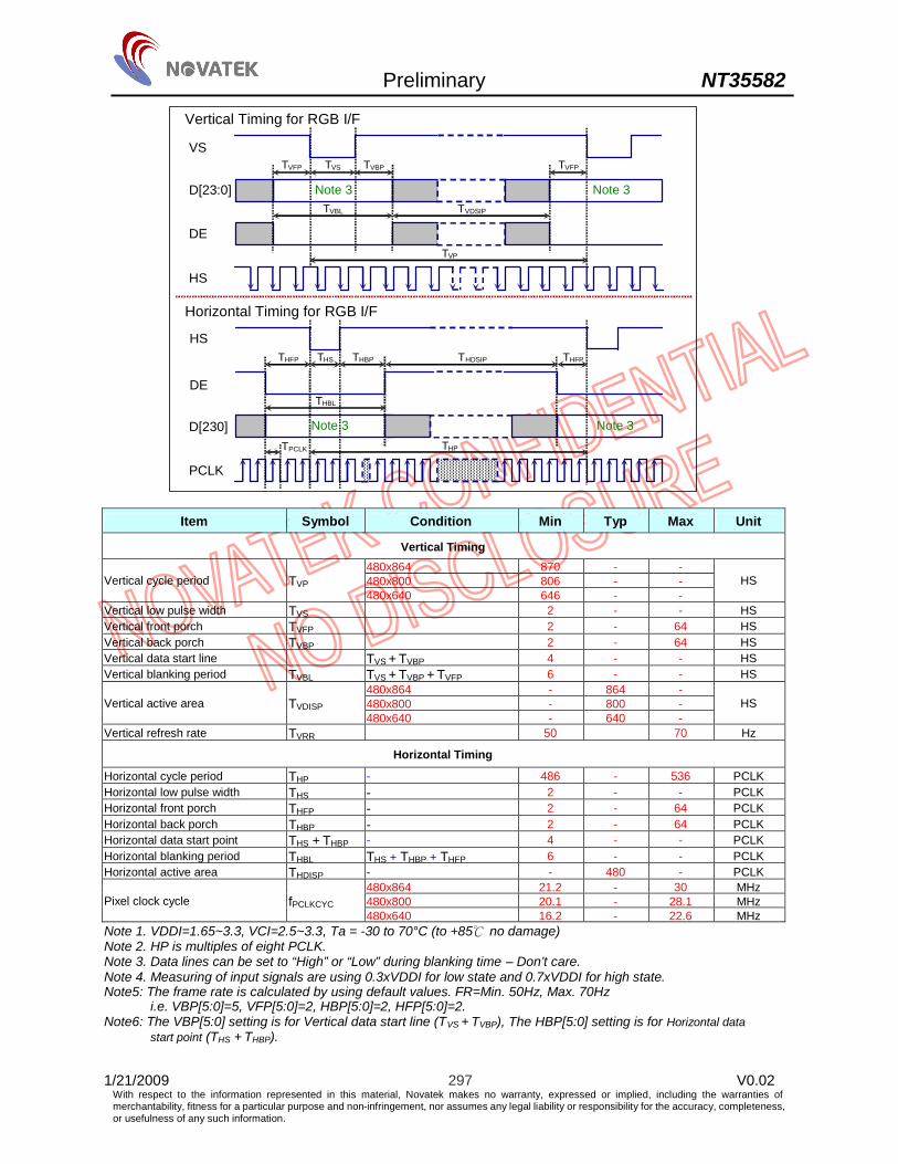
Preliminary NT35582
1/21/2009 297 V0.02 With respect to the information represented in this material, Novatek makes no warranty, expressed or implied, including the warranties of merchantability, fitness for a particular purpose and non-infringement, nor assumes any legal liability or responsibility for the accuracy, completeness, or usefulness of any such information.
Note 3 Note 3
TVS TVFPTVFP TVBP
TVP
TVDSIPTVBL
VS
D[23:0]
DE
HS
Vertical Timing for RGB I/F
TPCLK
Note 3 Note 3
THBPTHSTHFP THFPTHDSIP
THBL
THP
HS
DE
PCLK
D[230]
Horizontal Timing for RGB I/F
Item Symbol Condition Min Typ Max Unit
Vertical Timing 480x864 870 - - 480x800 806 - - Vertical cycle period TVP 480x640 646 - -
HS
Vertical low pulse width TVS 2 - - HS Vertical front porch TVFP 2 - 64 HS Vertical back porch TVBP 2 - 64 HS Vertical data start line TVS + TVBP 4 - - HS Vertical blanking period TVBL TVS + TVBP + TVFP 6 - - HS
480x864 - 864 - 480x800 - 800 - Vertical active area TVDISP 480x640 - 640 -
HS
Vertical refresh rate TVRR 50 70 Hz
Horizontal Timing
Horizontal cycle period THP - 486 - 536 PCLK Horizontal low pulse width THS - 2 - - PCLK Horizontal front porch THFP - 2 - 64 PCLK Horizontal back porch THBP - 2 - 64 PCLK Horizontal data start point THS + THBP - 4 - - PCLK Horizontal blanking period THBL THS + THBP + THFP 6 - - PCLK Horizontal active area THDISP - - 480 - PCLK
480x864 21.2 - 30 MHz 480x800 20.1 - 28.1 MHz Pixel clock cycle fPCLKCYC 480x640 16.2 - 22.6 MHz
Note 1. VDDI=1.65~3.3, VCI=2.5~3.3, Ta = -30 to 70°C (to +85 no damage) Note 2. HP is multiples of eight PCLK. Note 3. Data lines can be set to “High” or “Low” during blanking time – Don’t care. Note 4. Measuring of input signals are using 0.3xVDDI for low state and 0.7xVDDI for high state. Note5: The frame rate is calculated by using default values. FR=Min. 50Hz, Max. 70Hz i.e. VBP[5:0]=5, VFP[5:0]=2, HBP[5:0]=2, HFP[5:0]=2. Note6: The VBP[5:0] setting is for Vertical data start line (TVS + TVBP), The HBP[5:0] setting is for Horizontal data
start point (THS + THBP).

Preliminary NT35582
1/21/2009 298 V0.02 With respect to the information represented in this material, Novatek makes no warranty, expressed or implied, including the warranties of merchantability, fitness for a particular purpose and non-infringement, nor assumes any legal liability or responsibility for the accuracy, completeness, or usefulness of any such information.
7.3.7 I2C-Bus Timing Characteristics
Figure.114 I2C-Bus Operation
(VDDI=1.65~3.3, VCI=2.5~3.3, Ta = -30 to 70°C)
Item Symbol Timing Diagram Min. Typ. Max. Unit
Working Frequency Fclk Figure.114 - - 400 kHz
I2C Clock Low TckL Figure.114 1300 - - ns
I2C Clock High TckH Figure.114 600 - - ns
I2C Data ring time Tr Figure.114 - - 300 ns
I2C Data falling time Tf Figure.114 - - 300 ns
I2C Data hold time TDatHd Figure.114 0 - 900 ns
I2C Data setup time TDatSu Figure.114 100 - ns
I2C Start Condition hold time TStaHd Figure.114 600 - - ns
I2C Start Condition setup time TStaSu Figure.114 600 - - ns
I2C Stop Condition setup time TStpSu Figure.114 600 - - ns
I2C Bus free time TBusFree Figure.114 1300 - - ns

Preliminary NT35582
1/21/2009 299 V0.02 With respect to the information represented in this material, Novatek makes no warranty, expressed or implied, including the warranties of merchantability, fitness for a particular purpose and non-infringement, nor assumes any legal liability or responsibility for the accuracy, completeness, or usefulness of any such information.
7.3.8 Reset Timing Characteristics
tRESW
Shorter than 5μs
tREST
Normal Operation Resetting Initial Condition(Default for H/W reset)
RESX
Internal Status
Figure.115 Reset Operation
(VDDI=1.65~3.3, VCI=2.5~3.3, Ta = -30 to 70°C)
Item Symbol Timing Diagram Min. Typ. Max. Unit
Reset “Low” pulse width tRESW Figure.115 10 - - us
Command issue prohibit period after reset tREST Figure.115 20 - - ms

Preliminary NT35582
1/21/2009 300 V0.02 With respect to the information represented in this material, Novatek makes no warranty, expressed or implied, including the warranties of merchantability, fitness for a particular purpose and non-infringement, nor assumes any legal liability or responsibility for the accuracy, completeness, or usefulness of any such information.
7.3.9 Liquid Crystal Driver Output Characteristics
Tr
Source output (Sn)GVDD
Tr
Table 7.3.9 Liquid Crystal Driver Output Characteristics
Item Symbol Test Condition Min Typ Max Note Unit
Source-driver output stable time Tr
VCC = 1.5V, VDDI = 2.6 V, VCI=VDDAM=2.85V AVDD = 5.5V, GVDD = 4.80 V, 480 lines, 25oC, under default registers setting Load resistance is R = 6.5 kΩ, Load capacitance is C = 25 pF Time to reach the target voltage level +/-25mV
- - 3 us
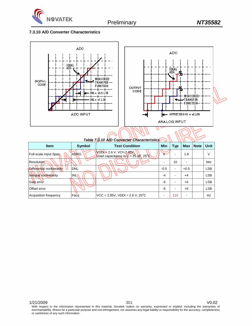
Preliminary NT35582
1/21/2009 301 V0.02 With respect to the information represented in this material, Novatek makes no warranty, expressed or implied, including the warranties of merchantability, fitness for a particular purpose and non-infringement, nor assumes any legal liability or responsibility for the accuracy, completeness, or usefulness of any such information.
7.3.10 A/D Converter Characteristics
Table 7.3.10 A/D Converter Characteristics Item Symbol Test Condition Min Typ Max Note Unit
Full-scale Input Span ADRG VDDI = 2.6 V, VCI=2.85V, Load capacitance is C = 25 pF, 25oC 0 - 1.8 V
Resolution - 10 - bits
Differential nonlinearity DNL -0.5 - +0.5 LSB
Integral nonlinearity INL -4 - +4 LSB
Gain error -6 - +6 LSB
Offset error -6 - +6 LSB
Acquisition frequency Facq VCC = 2.85V, VDDI = 2.6 V, 25oC - 110 - Hz

Preliminary NT35582
1/21/2009 302 V0.02 With respect to the information represented in this material, Novatek makes no warranty, expressed or implied, including the warranties of merchantability, fitness for a particular purpose and non-infringement, nor assumes any legal liability or responsibility for the accuracy, completeness, or usefulness of any such information.
8. Mechanical Characteristic 8.1 Chip Information
-Chip Size= 24000um x1700um (include Scribe Line) -Chip Thickness = 275um (Typical) -Bump height = 15m -Bump height tolerance +/- 3um
-Bump size tolerance: Output bump width: 21 um Output bump length: 60 um Input bump width: 25 um Input bump length: 60 um
8.2 Bump Information 8.2.1 Output Bump Dimension (Source/ Gate /Dummy)
Item Symbol Size Unit Bump pitch A 43.5 um Bump width C 21 um Bump height D 60 um Bump gap 1(output to output) B1 22.5 um Bump gap 2(gate signal to source) B2 59 um Bump gap 3(source to dummy) B3 41.5 um Bump area C x D 1260 um2 Chip Boundary(include scribe Lane) E 55 um
Boundary ( include scri be Lane)
EC B1
D
A B2
...
B3

Preliminary NT35582
1/21/2009 303 V0.02 With respect to the information represented in this material, Novatek makes no warranty, expressed or implied, including the warranties of merchantability, fitness for a particular purpose and non-infringement, nor assumes any legal liability or responsibility for the accuracy, completeness, or usefulness of any such information.
8.2.2 Input Bump Dimension
B
AE1
C
D
Bo undary(include scribe Lane)
E2E1
Boundary (include scribe line)
8.2.3 Alignment mark information
Item Symbol Size Unit Bump pitch B 50 um Bump width C 25 um Bump height D 60 um Bump gap 1( input to input) E1 25 um Bump gap 2( dummy to input) E2 30 um Bump area C x D 1500 um2 Chip Boundary(include scribe Lane) A 55 um
100
2525
25
25
25
10025
25
25
100
2525
100
25

Preliminary NT35582
1/21/2009 304 V0.02 With respect to the information represented in this material, Novatek makes no warranty, expressed or implied, including the warranties of merchantability, fitness for a particular purpose and non-infringement, nor assumes any legal liability or responsibility for the accuracy, completeness, or usefulness of any such information.
8.2.4 Bump Location and Dimension
24000

Preliminary NT35582
1/21/2009 305 V0.02 With respect to the information represented in this material, Novatek makes no warranty, expressed or implied, including the warranties of merchantability, fitness for a particular purpose and non-infringement, nor assumes any legal liability or responsibility for the accuracy, completeness, or usefulness of any such information.
8.3 Pad Coordinate
No Name X Y No Name X Y
1 DUMMY0 -11930 -765 47 VSS -9625 -765 2 VCOM -11875 -765 48 VSS -9575 -765 3 VCOM -11825 -765 49 VSS -9525 -765 4 VCOM -11775 -765 50 VSS -9475 -765 5 VCOM -11725 -765 51 VSS -9425 -765 6 VCOM -11675 -765 52 VSS -9375 -765 7 VCOM -11625 -765 53 VCL -9325 -765 8 VCOM -11575 -765 54 VCL -9275 -765 9 MTP_PWR -11525 -765 55 VCL -9225 -765 10 MTP_PWR -11475 -765 56 VCL -9175 -765 11 MTP_PWR -11425 -765 57 VCL -9125 -765 12 MTP_PWR -11375 -765 58 NVDD -9075 -765 13 MTP_PWR -11325 -765 59 NVDD -9025 -765 14 AVSS -11275 -765 60 NVDD -8975 -765 15 AVSS -11225 -765 61 NVDD -8925 -765 16 AVSS -11175 -765 62 NVDD -8875 -765 17 AVSS -11125 -765 63 AVSSR -8825 -765 18 AVSS -11075 -765 64 AVSSR -8775 -765 19 AVSS -11025 -765 65 AVSSR -8725 -765 20 VCI -10975 -765 66 TA1 -8675 -765 21 VCI -10925 -765 67 TA2 -8625 -765 22 VCI -10875 -765 68 VREF -8575 -765 23 VCI -10825 -765 69 VREF -8525 -765 24 VCI -10775 -765 70 VREF -8475 -765 25 VCI -10725 -765 71 VGMP -8425 -765 26 VCI -10675 -765 72 VGMP -8375 -765 27 VCI -10625 -765 73 VGMP -8325 -765 28 AVDD -10575 -765 74 VGSP -8275 -765 29 AVDD -10525 -765 75 VGSP -8225 -765 30 AVDD -10475 -765 76 VGSP -8175 -765 31 AVDD -10425 -765 77 VGMN -8125 -765 32 AVDD -10375 -765 78 VGMN -8075 -765 33 AVDD -10325 -765 79 VGMN -8025 -765 34 AVEE -10275 -765 80 VGSN -7975 -765 35 AVEE -10225 -765 81 VGSN -7925 -765 36 AVEE -10175 -765 82 VGSN -7875 -765 37 AVEE -10125 -765 83 ALS -7825 -765 38 AVEE -10075 -765 84 ALS -7775 -765 39 AVEE -10025 -765 85 AVSS -7725 -765 40 VCC -9975 -765 86 AVSS -7675 -765 41 VCC -9925 -765 87 AVSS -7625 -765 42 VCC -9875 -765 88 VSS -7575 -765 43 VCC -9825 -765 89 VSS -7525 -765 44 VCC -9775 -765 90 VSS -7475 -765 45 VCC -9725 -765 91 VSS -7425 -765 46 VSS -9675 -765 92 VDDI -7375 -765

Preliminary NT35582
1/21/2009 306 V0.02 With respect to the information represented in this material, Novatek makes no warranty, expressed or implied, including the warranties of merchantability, fitness for a particular purpose and non-infringement, nor assumes any legal liability or responsibility for the accuracy, completeness, or usefulness of any such information.
No Name X Y No Name X Y
93 VDDI -7325 -765 139 D16 -5025 -765 94 VDDI -7275 -765 140 D15 -4975 -765 95 VDDI -7225 -765 141 D15 -4925 -765 96 FTE -7175 -765 142 D14 -4875 -765 97 SDO -7125 -765 143 D14 -4825 -765 98 SDI/I2C_SDA -7075 -765 144 D13 -4775 -765 99 DCX -7025 -765 145 D13 -4725 -765 100 WRX/SCL/I2C_SCL -6975 -765 146 D12 -4675 -765 101 WRX/SCL/I2C_SCL -6925 -765 147 D12 -4625 -765 102 RDX -6875 -765 148 D11 -4575 -765 103 CSX -6825 -765 149 D11 -4525 -765 104 RESX -6775 -765 150 D10 -4475 -765 105 TEST -6725 -765 151 D10 -4425 -765 106 TEST -6675 -765 152 D9 -4375 -765 107 VDDIO -6625 -765 153 D9 -4325 -765 108 SA0 -6575 -765 154 D8 -4275 -765 109 SA1 -6525 -765 155 D8 -4225 -765 110 IM0 -6475 -765 156 D7 -4175 -765 111 IM1 -6425 -765 157 D7 -4125 -765 112 IM2 -6375 -765 158 D6 -4075 -765 113 IM3 -6325 -765 159 D6 -4025 -765 114 GM0 -6275 -765 160 D5 -3975 -765 115 GM1 -6225 -765 161 D5 -3925 -765 116 GM2 -6175 -765 162 D4 -3875 -765 117 PNL -6125 -765 163 D4 -3825 -765 118 FRM -6075 -765 164 D3 -3775 -765 119 NBWSEL -6025 -765 165 D3 -3725 -765 120 RL -5975 -765 166 D2 -3675 -765 121 TB -5925 -765 167 D2 -3625 -765 122 SHUT -5875 -765 168 D1 -3575 -765 123 VSSIO -5825 -765 169 D1 -3525 -765 124 D23 -5775 -765 170 D0 -3475 -765 125 D23 -5725 -765 171 D0 -3425 -765 126 D22 -5675 -765 172 DE -3375 -765 127 D22 -5625 -765 173 PCLK -3325 -765 128 D21 -5575 -765 174 PCLK -3275 -765 129 D21 -5525 -765 175 HS -3225 -765 130 D20 -5475 -765 176 VS -3175 -765 131 D20 -5425 -765 177 VDDI -3125 -765 132 D19 -5375 -765 178 VDDI -3075 -765 133 D19 -5325 -765 179 VDDI -3025 -765 134 D18 -5275 -765 180 VDDI -2975 -765 135 D18 -5225 -765 181 OSC -2925 -765 136 D17 -5175 -765 182 OSC -2875 -765 137 D17 -5125 -765 183 LED_PWM -2825 -765 138 D16 -5075 -765 184 LED_PWM -2775 -765
Preliminary NT35582
1/21/2009 307 V0.02 With respect to the information represented in this material, Novatek makes no warranty, expressed or implied, including the warranties of merchantability, fitness for a particular purpose and non-infringement, nor assumes any legal liability or responsibility for the accuracy, completeness, or usefulness of any such information.
No Name X Y No Name X Y
185 LED_ON -2725 -765 231 VG_MDDI -425 -765 186 VSS -2675 -765 232 VG_MDDI -375 -765 187 VSS -2625 -765 233 MDDI_STB_M -325 -765 188 VSS -2575 -765 234 MDDI_STB_M -275 -765 189 VSS -2525 -765 235 MDDI_STB_M -225 -765 190 AVEE -2475 -765 236 VG_MDDI -175 -765 191 AVEE -2425 -765 237 VG_MDDI -125 -765 192 AVEE -2375 -765 238 MDDI_STB_P -75 -765 193 AVEE -2325 -765 239 MDDI_STB_P -25 -765 194 AVDD -2275 -765 240 MDDI_STB_P 25 -765 195 AVDD -2225 -765 241 VG_MDDI 75 -765 196 AVDD -2175 -765 242 VG_MDDI 125 -765 197 AVDD -2125 -765 243 MDDI_DATA_M 175 -765 198 AVDD -2075 -765 244 MDDI_DATA_M 225 -765 199 AVSS -2025 -765 245 MDDI_DATA_M 275 -765 200 AVSS -1975 -765 246 VG_MDDI 325 -765 201 AVSS -1925 -765 247 VG_MDDI 375 -765 202 AVSS -1875 -765 248 MDDI_DATA_P 425 -765 203 VCC -1825 -765 249 MDDI_DATA_P 475 -765 204 VCC -1775 -765 250 MDDI_DATA_P 525 -765 205 VCC -1725 -765 251 VG_MDDI 575 -765 206 VCC -1675 -765 252 VG_MDDI 625 -765 207 VCC -1625 -765 253 AVSS 675 -765 208 VCC -1575 -765 254 AVSS 725 -765 209 VCC -1525 -765 255 AVSS 775 -765 210 VCC -1475 -765 256 AVSS 825 -765 211 VDDAM -1425 -765 257 AVSS 875 -765 212 VDDAM -1375 -765 258 VSS 925 -765 213 VDDAM -1325 -765 259 VSS 975 -765 214 VDDAM -1275 -765 260 VSS 1025 -765 215 VDDAM -1225 -765 261 VSS 1075 -765 216 VDDAM -1175 -765 262 VSS 1125 -765 217 VDDAM -1125 -765 263 VGH 1175 -765 218 VP_MDDI -1075 -765 264 VGH 1225 -765 219 VP_MDDI -1025 -765 265 VGH 1275 -765 220 VP_MDDI -975 -765 266 VGH 1325 -765 221 VP_MDDI -925 -765 267 VGH 1375 -765 222 VP_MDDI -875 -765 268 C41N 1425 -765 223 VP_MDDI -825 -765 269 C41N 1475 -765 224 VP_MDDI -775 -765 270 C41N 1525 -765 225 VG_MDDI -725 -765 271 C41N 1575 -765 226 VG_MDDI -675 -765 272 C41P 1625 -765 227 VG_MDDI -625 -765 273 C41P 1675 -765 228 VG_MDDI -575 -765 274 C41P 1725 -765 229 VG_MDDI -525 -765 275 C41P 1775 -765 230 VG_MDDI -475 -765 276 VGL 1825 -765

Preliminary NT35582
1/21/2009 308 V0.02 With respect to the information represented in this material, Novatek makes no warranty, expressed or implied, including the warranties of merchantability, fitness for a particular purpose and non-infringement, nor assumes any legal liability or responsibility for the accuracy, completeness, or usefulness of any such information.
No Name X Y No Name X Y
277 VGL 1875 -765 323 CVSS 4175 -765 278 VGL 1925 -765 324 CVSS 4225 -765 279 VGL 1975 -765 325 CVSS 4275 -765 280 VGL 2025 -765 326 AVEE 4325 -765 281 C51N 2075 -765 327 AVEE 4375 -765 282 C51N 2125 -765 328 AVEE 4425 -765 283 C51N 2175 -765 329 AVEE 4475 -765 284 C51N 2225 -765 330 AVEE 4525 -765 285 C51P 2275 -765 331 AVEE 4575 -765 286 C51P 2325 -765 332 AVEE 4625 -765 287 C51P 2375 -765 333 AVEE 4675 -765 288 C51P 2425 -765 334 C24N 4725 -765 289 VCI 2475 -765 335 C24N 4775 -765 290 VCI 2525 -765 336 C24N 4825 -765 291 VCI 2575 -765 337 C24N 4875 -765 292 VCI 2625 -765 338 C24N 4925 -765 293 VCI 2675 -765 339 C24N 4975 -765 294 C32N 2725 -765 340 C24P 5025 -765 295 C32N 2775 -765 341 C24P 5075 -765 296 C32N 2825 -765 342 C24P 5125 -765 297 C32N 2875 -765 343 C24P 5175 -765 298 C32N 2925 -765 344 C24P 5225 -765 299 C32P 2975 -765 345 C24P 5275 -765 300 C32P 3025 -765 346 VCI 5325 -765 301 C32P 3075 -765 347 VCI 5375 -765 302 C32P 3125 -765 348 VCI 5425 -765 303 C32P 3175 -765 349 VCI 5475 -765 304 C31N 3225 -765 350 C23N 5525 -765 305 C31N 3275 -765 351 C23N 5575 -765 306 C31N 3325 -765 352 C23N 5625 -765 307 C31N 3375 -765 353 C23N 5675 -765 308 C31N 3425 -765 354 C23N 5725 -765 309 C31P 3475 -765 355 C23N 5775 -765 310 C31P 3525 -765 356 C23P 5825 -765 311 C31P 3575 -765 357 C23P 5875 -765 312 C31P 3625 -765 358 C23P 5925 -765 313 C31P 3675 -765 359 C23P 5975 -765 314 VCL 3725 -765 360 C23P 6025 -765 315 VCL 3775 -765 361 C23P 6075 -765 316 VCL 3825 -765 362 CVSS 6125 -765 317 VCL 3875 -765 363 CVSS 6175 -765 318 VCL 3925 -765 364 CVSS 6225 -765 319 VCL 3975 -765 365 CVSS 6275 -765 320 CVSS 4025 -765 366 C22N 6325 -765 321 CVSS 4075 -765 367 C22N 6375 -765 322 CVSS 4125 -765 368 C22N 6425 -765

Preliminary NT35582
1/21/2009 309 V0.02 With respect to the information represented in this material, Novatek makes no warranty, expressed or implied, including the warranties of merchantability, fitness for a particular purpose and non-infringement, nor assumes any legal liability or responsibility for the accuracy, completeness, or usefulness of any such information.
No Name X Y No Name X Y
369 C22N 6475 -765 415 AVDD 8775 -765 370 C22N 6525 -765 416 C14N 8825 -765 371 C22N 6575 -765 417 C14N 8875 -765 372 C22P 6625 -765 418 C14N 8925 -765 373 C22P 6675 -765 419 C14N 8975 -765 374 C22P 6725 -765 420 C14N 9025 -765 375 C22P 6775 -765 421 C14N 9075 -765 376 C22P 6825 -765 422 C14P 9125 -765 377 C22P 6875 -765 423 C14P 9175 -765 378 VCI 6925 -765 424 C14P 9225 -765 379 VCI 6975 -765 425 C14P 9275 -765 380 VCI 7025 -765 426 C14P 9325 -765 381 VCI 7075 -765 427 C14P 9375 -765 382 C21N 7125 -765 428 VCI 9425 -765 383 C21N 7175 -765 429 VCI 9475 -765 384 C21N 7225 -765 430 VCI 9525 -765 385 C21N 7275 -765 431 VCI 9575 -765 386 C21N 7325 -765 432 C13N 9625 -765 387 C21N 7375 -765 433 C13N 9675 -765 388 C21P 7425 -765 434 C13N 9725 -765 389 C21P 7475 -765 435 C13N 9775 -765 390 C21P 7525 -765 436 C13N 9825 -765 391 C21P 7575 -765 437 C13N 9875 -765 392 C21P 7625 -765 438 C13P 9925 -765 393 C21P 7675 -765 439 C13P 9975 -765 394 CVSS 7725 -765 440 C13P 10025 -765 395 CVSS 7775 -765 441 C13P 10075 -765 396 CVSS 7825 -765 442 C13P 10125 -765 397 CVSS 7875 -765 443 C13P 10175 -765 398 AVSS 7925 -765 444 CVSS 10225 -765 399 AVSS 7975 -765 445 CVSS 10275 -765 400 AVSS 8025 -765 446 CVSS 10325 -765 401 AVSS 8075 -765 447 CVSS 10375 -765 402 AVSS 8125 -765 448 C12N 10425 -765 403 VSS 8175 -765 449 C12N 10475 -765 404 VSS 8225 -765 450 C12N 10525 -765 405 VSS 8275 -765 451 C12N 10575 -765 406 VSS 8325 -765 452 C12N 10625 -765 407 VSS 8375 -765 453 C12N 10675 -765 408 AVDD 8425 -765 454 C12P 10725 -765 409 AVDD 8475 -765 455 C12P 10775 -765 410 AVDD 8525 -765 456 C12P 10825 -765 411 AVDD 8575 -765 457 C12P 10875 -765 412 AVDD 8625 -765 458 C12P 10925 -765 413 AVDD 8675 -765 459 C12P 10975 -765 414 AVDD 8725 -765 460 VCI 11025 -765

Preliminary NT35582
1/21/2009 310 V0.02 With respect to the information represented in this material, Novatek makes no warranty, expressed or implied, including the warranties of merchantability, fitness for a particular purpose and non-infringement, nor assumes any legal liability or responsibility for the accuracy, completeness, or usefulness of any such information.
No Name X Y No Name X Y
461 VCI 11075 -765 507 S10 10546 765 462 VCI 11125 -765 508 S11 10502.5 765 463 VCI 11175 -765 509 S12 10459 765 464 C11N 11225 -765 510 S13 10415.5 765 465 C11N 11275 -765 511 S14 10372 765 466 C11N 11325 -765 512 S15 10328.5 765 467 C11N 11375 -765 513 S16 10285 765 468 C11N 11425 -765 514 S17 10241.5 765 469 C11N 11475 -765 515 S18 10198 765 470 C11P 11525 -765 516 S19 10154.5 765 471 C11P 11575 -765 517 S20 10111 765 472 C11P 11625 -765 518 S21 10067.5 765 473 C11P 11675 -765 519 S22 10024 765 474 C11P 11725 -765 520 S23 9980.5 765 475 C11P 11775 -765 521 S24 9937 765 476 CAMP_REF 11825 -765 522 S25 9893.5 765 477 CAMP_REF 11875 -765 523 S26 9850 765 478 DUMMY1 11930 -765 524 S27 9806.5 765 479 VGH 11800.5 765 525 S28 9763 765 480 VGH 11757 765 526 S29 9719.5 765 481 VGL 11713.5 765 527 S30 9676 765 482 VGL 11670 765 528 S31 9632.5 765 483 STV_R 11626.5 765 529 S32 9589 765 484 CLK_R 11583 765 530 S33 9545.5 765 485 XCLK_R 11539.5 765 531 S34 9502 765 486 U2D_R 11496 765 532 S35 9458.5 765 487 D2U_R 11452.5 765 533 S36 9415 765 488 XDON_R 11409 765 534 S37 9371.5 765 489 XDONB_R 11365.5 765 535 S38 9328 765 490 CTRL6 11322 765 536 S39 9284.5 765 491 CTRL5 11278.5 765 537 S40 9241 765 492 CTRL4 11235 765 538 S41 9197.5 765 493 CTRL3 11191.5 765 539 S42 9154 765 494 CTRL2 11148 765 540 S43 9110.5 765 495 CTRL1 11104.5 765 541 S44 9067 765 496 SDUM0 11024.5 765 542 S45 9023.5 765 497 SDUM1 10981 765 543 S46 8980 765 498 S1 10937.5 765 544 S47 8936.5 765 499 S2 10894 765 545 S48 8893 765 500 S3 10850.5 765 546 S49 8849.5 765 501 S4 10807 765 547 S50 8806 765 502 S5 10763.5 765 548 S51 8762.5 765 503 S6 10720 765 549 S52 8719 765 504 S7 10676.5 765 550 S53 8675.5 765 505 S8 10633 765 551 S54 8632 765 506 S9 10589.5 765 552 S55 8588.5 765

Preliminary NT35582
1/21/2009 311 V0.02 With respect to the information represented in this material, Novatek makes no warranty, expressed or implied, including the warranties of merchantability, fitness for a particular purpose and non-infringement, nor assumes any legal liability or responsibility for the accuracy, completeness, or usefulness of any such information.
No Name X Y No Name X Y
553 S56 8545 765 599 S102 6544 765 554 S57 8501.5 765 600 S103 6500.5 765 555 S58 8458 765 601 S104 6457 765 556 S59 8414.5 765 602 S105 6413.5 765 557 S60 8371 765 603 S106 6370 765 558 S61 8327.5 765 604 S107 6326.5 765 559 S62 8284 765 605 S108 6283 765 560 S63 8240.5 765 606 S109 6239.5 765 561 S64 8197 765 607 S110 6196 765 562 S65 8153.5 765 608 S111 6152.5 765 563 S66 8110 765 609 S112 6109 765 564 S67 8066.5 765 610 S113 6065.5 765 565 S68 8023 765 611 S114 6022 765 566 S69 7979.5 765 612 S115 5978.5 765 567 S70 7936 765 613 S116 5935 765 568 S71 7892.5 765 614 S117 5891.5 765 569 S72 7849 765 615 S118 5848 765 570 S73 7805.5 765 616 S119 5804.5 765 571 S74 7762 765 617 S120 5761 765 572 S75 7718.5 765 618 S121 5717.5 765 573 S76 7675 765 619 S122 5674 765 574 S77 7631.5 765 620 S123 5630.5 765 575 S78 7588 765 621 S124 5587 765 576 S79 7544.5 765 622 S125 5543.5 765 577 S80 7501 765 623 S126 5500 765 578 S81 7457.5 765 624 S127 5456.5 765 579 S82 7414 765 625 S128 5413 765 580 S83 7370.5 765 626 S129 5369.5 765 581 S84 7327 765 627 S130 5326 765 582 S85 7283.5 765 628 S131 5282.5 765 583 S86 7240 765 629 S132 5239 765 584 S87 7196.5 765 630 S133 5195.5 765 585 S88 7153 765 631 S134 5152 765 586 S89 7109.5 765 632 S135 5108.5 765 587 S90 7066 765 633 S136 5065 765 588 S91 7022.5 765 634 S137 5021.5 765 589 S92 6979 765 635 S138 4978 765 590 S93 6935.5 765 636 S139 4934.5 765 591 S94 6892 765 637 S140 4891 765 592 S95 6848.5 765 638 S141 4847.5 765 593 S96 6805 765 639 S142 4804 765 594 S97 6761.5 765 640 S143 4760.5 765 595 S98 6718 765 641 S144 4717 765 596 S99 6674.5 765 642 S145 4673.5 765 597 S100 6631 765 643 S146 4630 765 598 S101 6587.5 765 644 S147 4586.5 765
Preliminary NT35582
1/21/2009 312 V0.02 With respect to the information represented in this material, Novatek makes no warranty, expressed or implied, including the warranties of merchantability, fitness for a particular purpose and non-infringement, nor assumes any legal liability or responsibility for the accuracy, completeness, or usefulness of any such information.
No Name X Y No Name X Y
645 S148 4543 765 691 S194 2542 765 646 S149 4499.5 765 692 S195 2498.5 765 647 S150 4456 765 693 S196 2455 765 648 S151 4412.5 765 694 S197 2411.5 765 649 S152 4369 765 695 S198 2368 765 650 S153 4325.5 765 696 S199 2324.5 765 651 S154 4282 765 697 S200 2281 765 652 S155 4238.5 765 698 S201 2237.5 765 653 S156 4195 765 699 S202 2194 765 654 S157 4151.5 765 700 S203 2150.5 765 655 S158 4108 765 701 S204 2107 765 656 S159 4064.5 765 702 S205 2063.5 765 657 S160 4021 765 703 S206 2020 765 658 S161 3977.5 765 704 S207 1976.5 765 659 S162 3934 765 705 S208 1933 765 660 S163 3890.5 765 706 S209 1889.5 765 661 S164 3847 765 707 S210 1846 765 662 S165 3803.5 765 708 S211 1802.5 765 663 S166 3760 765 709 S212 1759 765 664 S167 3716.5 765 710 S213 1715.5 765 665 S168 3673 765 711 S214 1672 765 666 S169 3629.5 765 712 S215 1628.5 765 667 S170 3586 765 713 S216 1585 765 668 S171 3542.5 765 714 S217 1541.5 765 669 S172 3499 765 715 S218 1498 765 670 S173 3455.5 765 716 S219 1454.5 765 671 S174 3412 765 717 S220 1411 765 672 S175 3368.5 765 718 S221 1367.5 765 673 S176 3325 765 719 S222 1324 765 674 S177 3281.5 765 720 S223 1280.5 765 675 S178 3238 765 721 S224 1237 765 676 S179 3194.5 765 722 S225 1193.5 765 677 S180 3151 765 723 S226 1150 765 678 S181 3107.5 765 724 S227 1106.5 765 679 S182 3064 765 725 S228 1063 765 680 S183 3020.5 765 726 S229 1019.5 765 681 S184 2977 765 727 S230 976 765 682 S185 2933.5 765 728 S231 932.5 765 683 S186 2890 765 729 S232 889 765 684 S187 2846.5 765 730 S233 845.5 765 685 S188 2803 765 731 S234 802 765 686 S189 2759.5 765 732 S235 758.5 765 687 S190 2716 765 733 S236 715 765 688 S191 2672.5 765 734 S237 671.5 765 689 S192 2629 765 735 S238 628 765 690 S193 2585.5 765 736 S239 584.5 765

Preliminary NT35582
1/21/2009 313 V0.02 With respect to the information represented in this material, Novatek makes no warranty, expressed or implied, including the warranties of merchantability, fitness for a particular purpose and non-infringement, nor assumes any legal liability or responsibility for the accuracy, completeness, or usefulness of any such information.
No Name X Y No Name X Y
737 S240 541 765 783 S263 -1498 765 738 DUMMY2 478.5 765 784 S264 -1541.5 765 739 DUMMY3 435 765 785 S265 -1585 765 740 DUMMY4 391.5 765 786 S266 -1628.5 765 741 DUMMY5 348 765 787 S267 -1672 765 742 DUMMY6 304.5 765 788 S268 -1715.5 765 743 DUMMY7 261 765 789 S269 -1759 765 744 DUMMY8 217.5 765 790 S270 -1802.5 765 745 DUMMY9 174 765 791 S271 -1846 765 746 DUMMY10 130.5 765 792 S272 -1889.5 765 747 DUMMY11 87 765 793 S273 -1933 765 748 DUMMY12 43.5 765 794 S274 -1976.5 765 749 DUMMY13 0 765 795 S275 -2020 765 750 DUMMY14 -43.5 765 796 S276 -2063.5 765 751 DUMMY15 -87 765 797 S277 -2107 765 752 DUMMY16 -130.5 765 798 S278 -2150.5 765 753 DUMMY17 -174 765 799 S279 -2194 765 754 DUMMY18 -217.5 765 800 S280 -2237.5 765 755 DUMMY19 -261 765 801 S281 -2281 765 756 DUMMY20 -304.5 765 802 S282 -2324.5 765 757 DUMMY21 -348 765 803 S283 -2368 765 758 DUMMY22 -391.5 765 804 S284 -2411.5 765 759 DUMMY23 -435 765 805 S285 -2455 765 760 DUMMY24 -478.5 765 806 S286 -2498.5 765 761 S241 -541 765 807 S287 -2542 765 762 S242 -584.5 765 808 S288 -2585.5 765 763 S243 -628 765 809 S289 -2629 765 764 S244 -671.5 765 810 S290 -2672.5 765 765 S245 -715 765 811 S291 -2716 765 766 S246 -758.5 765 812 S292 -2759.5 765 767 S247 -802 765 813 S293 -2803 765 768 S248 -845.5 765 814 S294 -2846.5 765 769 S249 -889 765 815 S295 -2890 765 770 S250 -932.5 765 816 S296 -2933.5 765 771 S251 -976 765 817 S297 -2977 765 772 S252 -1019.5 765 818 S298 -3020.5 765 773 S253 -1063 765 819 S299 -3064 765 774 S254 -1106.5 765 820 S300 -3107.5 765 775 S255 -1150 765 821 S301 -3151 765 776 S256 -1193.5 765 822 S302 -3194.5 765 777 S257 -1237 765 823 S303 -3238 765 778 S258 -1280.5 765 824 S304 -3281.5 765 779 S259 -1324 765 825 S305 -3325 765 780 S260 -1367.5 765 826 S306 -3368.5 765 781 S261 -1411 765 827 S307 -3412 765 782 S262 -1454.5 765 828 S308 -3455.5 765

Preliminary NT35582
1/21/2009 314 V0.02 With respect to the information represented in this material, Novatek makes no warranty, expressed or implied, including the warranties of merchantability, fitness for a particular purpose and non-infringement, nor assumes any legal liability or responsibility for the accuracy, completeness, or usefulness of any such information.
No Name X Y No Name X Y
829 S309 -3499 765 875 S355 -5500 765 830 S310 -3542.5 765 876 S356 -5543.5 765 831 S311 -3586 765 877 S357 -5587 765 832 S312 -3629.5 765 878 S358 -5630.5 765 833 S313 -3673 765 879 S359 -5674 765 834 S314 -3716.5 765 880 S360 -5717.5 765 835 S315 -3760 765 881 S361 -5761 765 836 S316 -3803.5 765 882 S362 -5804.5 765 837 S317 -3847 765 883 S363 -5848 765 838 S318 -3890.5 765 884 S364 -5891.5 765 839 S319 -3934 765 885 S365 -5935 765 840 S320 -3977.5 765 886 S366 -5978.5 765 841 S321 -4021 765 887 S367 -6022 765 842 S322 -4064.5 765 888 S368 -6065.5 765 843 S323 -4108 765 889 S369 -6109 765 844 S324 -4151.5 765 890 S370 -6152.5 765 845 S325 -4195 765 891 S371 -6196 765 846 S326 -4238.5 765 892 S372 -6239.5 765 847 S327 -4282 765 893 S373 -6283 765 848 S328 -4325.5 765 894 S374 -6326.5 765 849 S329 -4369 765 895 S375 -6370 765 850 S330 -4412.5 765 896 S376 -6413.5 765 851 S331 -4456 765 897 S377 -6457 765 852 S332 -4499.5 765 898 S378 -6500.5 765 853 S333 -4543 765 899 S379 -6544 765 854 S334 -4586.5 765 900 S380 -6587.5 765 855 S335 -4630 765 901 S381 -6631 765 856 S336 -4673.5 765 902 S382 -6674.5 765 857 S337 -4717 765 903 S383 -6718 765 858 S338 -4760.5 765 904 S384 -6761.5 765 859 S339 -4804 765 905 S385 -6805 765 860 S340 -4847.5 765 906 S386 -6848.5 765 861 S341 -4891 765 907 S387 -6892 765 862 S342 -4934.5 765 908 S388 -6935.5 765 863 S343 -4978 765 909 S389 -6979 765 864 S344 -5021.5 765 910 S390 -7022.5 765 865 S345 -5065 765 911 S391 -7066 765 866 S346 -5108.5 765 912 S392 -7109.5 765 867 S347 -5152 765 913 S393 -7153 765 868 S348 -5195.5 765 914 S394 -7196.5 765 869 S349 -5239 765 915 S395 -7240 765 870 S350 -5282.5 765 916 S396 -7283.5 765 871 S351 -5326 765 917 S397 -7327 765 872 S352 -5369.5 765 918 S398 -7370.5 765 873 S353 -5413 765 919 S399 -7414 765 874 S354 -5456.5 765 920 S400 -7457.5 765
Preliminary NT35582
1/21/2009 315 V0.02 With respect to the information represented in this material, Novatek makes no warranty, expressed or implied, including the warranties of merchantability, fitness for a particular purpose and non-infringement, nor assumes any legal liability or responsibility for the accuracy, completeness, or usefulness of any such information.
No Name X Y No Name X Y
921 S401 -7501 765 967 S447 -9502 765 922 S402 -7544.5 765 968 S448 -9545.5 765 923 S403 -7588 765 969 S449 -9589 765 924 S404 -7631.5 765 970 S450 -9632.5 765 925 S405 -7675 765 971 S451 -9676 765 926 S406 -7718.5 765 972 S452 -9719.5 765 927 S407 -7762 765 973 S453 -9763 765 928 S408 -7805.5 765 974 S454 -9806.5 765 929 S409 -7849 765 975 S455 -9850 765 930 S410 -7892.5 765 976 S456 -9893.5 765 931 S411 -7936 765 977 S457 -9937 765 932 S412 -7979.5 765 978 S458 -9980.5 765 933 S413 -8023 765 979 S459 -10024 765 934 S414 -8066.5 765 980 S460 -10067.5 765 935 S415 -8110 765 981 S461 -10111 765 936 S416 -8153.5 765 982 S462 -10154.5 765 937 S417 -8197 765 983 S463 -10198 765 938 S418 -8240.5 765 984 S464 -10241.5 765 939 S419 -8284 765 985 S465 -10285 765 940 S420 -8327.5 765 986 S466 -10328.5 765 941 S421 -8371 765 987 S467 -10372 765 942 S422 -8414.5 765 988 S468 -10415.5 765 943 S423 -8458 765 989 S469 -10459 765 944 S424 -8501.5 765 990 S470 -10502.5 765 945 S425 -8545 765 991 S471 -10546 765 946 S426 -8588.5 765 992 S472 -10589.5 765 947 S427 -8632 765 993 S473 -10633 765 948 S428 -8675.5 765 994 S474 -10676.5 765 949 S429 -8719 765 995 S475 -10720 765 950 S430 -8762.5 765 996 S476 -10763.5 765 951 S431 -8806 765 997 S477 -10807 765 952 S432 -8849.5 765 998 S478 -10850.5 765 953 S433 -8893 765 999 S479 -10894 765 954 S434 -8936.5 765 1000 S480 -10937.5 765 955 S435 -8980 765 1001 SDUM2 -10981 765 956 S436 -9023.5 765 1002 SDUM3 -11024.5 765 957 S437 -9067 765 1003 SW3 -11104.5 765 958 S438 -9110.5 765 1004 SW3 -11148 765 959 S439 -9154 765 1005 SW2 -11191.5 765 960 S440 -9197.5 765 1006 SW2 -11235 765 961 S441 -9241 765 1007 SW1 -11278.5 765 962 S442 -9284.5 765 1008 SW1 -11322 765 963 S443 -9328 765 1009 XDONB_L -11365.5 765 964 S444 -9371.5 765 1010 XDON_L -11409 765 965 S445 -9415 765 1011 D2U_L -11452.5 765 966 S446 -9458.5 765 1012 U2D_L -11496 765
Preliminary NT35582
1/21/2009 316 V0.02 With respect to the information represented in this material, Novatek makes no warranty, expressed or implied, including the warranties of merchantability, fitness for a particular purpose and non-infringement, nor assumes any legal liability or responsibility for the accuracy, completeness, or usefulness of any such information.
No Name X Y No Name X Y
1013 XCLK_L -11539.5 765 1014 CLK_L -11583 765 1015 STV_L -11626.5 765 1016 VGL -11670 765 1017 VGL -11713.5 765 1018 VGH -11757 765 1019 VGH -11800.5 765 1020 ALK-L -11885 745 1021 ALK-R 11885 745
Related Documents
![Untitled Document []€¦ · Title: Untitled Document Created Date: 191000309095417](https://static.cupdf.com/doc/110x72/600101983d1deb13132b1db7/untitled-document-title-untitled-document-created-date-191000309095417.jpg)
![Untitled-1 []...Title Untitled-1 Author Eric Created Date 20161101174004Z](https://static.cupdf.com/doc/110x72/5e29343b7bac0544ab7cede9/-untitled-1-title-untitled-1-author-eric-created-date-20161101174004z.jpg)
![Untitled-1 [amadas.com] · Title: Untitled-1 Author: mikee Subject: Untitled-1 Created Date: 191000407142803](https://static.cupdf.com/doc/110x72/5f91617c574a7c792f76c110/untitled-1-title-untitled-1-author-mikee-subject-untitled-1-created-date.jpg)
![Untitled-5 [unstats.un.org]...Title Untitled-5 Created Date 20010118111809Z](https://static.cupdf.com/doc/110x72/60389b95586a40652f159b99/-untitled-5-title-untitled-5-created-date-20010118111809z.jpg)


![Untitled-1 []€¦ · Title: Untitled-1 Created Date: 20140217113650Z](https://static.cupdf.com/doc/110x72/60d0fe286b308346f174d731/untitled-1-title-untitled-1-created-date-20140217113650z.jpg)
![Untitled-2 [] · Title: Untitled-2 Author: richard Created Date: 20191024090411Z](https://static.cupdf.com/doc/110x72/601503f4b4351525204ed534/untitled-2-title-untitled-2-author-richard-created-date-20191024090411z.jpg)
![Untitled-5 [] · Title: Untitled-5 Created Date: 20010118111809Z](https://static.cupdf.com/doc/110x72/5f88abbf1b028837b776432c/untitled-5-title-untitled-5-created-date-20010118111809z.jpg)
![Untitled-3 [] · Title: Untitled-3 Created Date: 20171219145635Z](https://static.cupdf.com/doc/110x72/5ecefdc3d3b4604bd43ef198/untitled-3-title-untitled-3-created-date-20171219145635z.jpg)
![Untitled 2 [agonzalezclasses.weebly.com] · Title: Untitled 2.pages Created Date: 20180822234525Z](https://static.cupdf.com/doc/110x72/5ffaf3683ef3eb57ec5ac37a/untitled-2-title-untitled-2pages-created-date-20180822234525z.jpg)
![Untitled-2 [shaunthesheep.s3.amazonaws.com]Title Untitled-2 Created Date 20141223102645Z](https://static.cupdf.com/doc/110x72/5fd38d55ced95a4f656cdf32/-untitled-2-shaunthesheeps3-title-untitled-2-created-date-20141223102645z.jpg)